n- and p-channel enhancement mode power mosfet mtc3588n6ftp01.cystekec.com/mtc3588n6.pdf ·...
TRANSCRIPT

CYStech Electronics Corp.
Spec. No. : C102N6 Issued Date : 2015.08.13 Revised Date : 2017.03.30 Page No. : 1/12
MTC3588N6 CYStek Product Specification
N- And P-Channel Enhancement Mode Power MOSFET
MTC3588N6 N-CH P-CH BVDSS 14V -14V ID @ TA=25 °C 5.4A(VGS=4.5V) -3.6A(VGS=-4.5 V)
17.6mΩ(VGS=4.5V) 45.1mΩ(VGS=-4.5V) RDSON(TYP.) 24.7mΩ(VGS=2.5V) 65.6mΩ(VGS=-2.5V)
Features • Simple drive requirement • Low gate charge • Low on-resistance • Fast switching speed • Pb-free lead plating and halogen-free package
Equivalent Circuit Outline
Ordering Information
Device Package Shipping
MTC3588N6-0-T1-G SOT-26 (Pb-free lead plating and halogen-free package) 3000 pcs / Tape & Reel
MTC3588N6 SOT-26
D2 S1
D1
G:Gate S:Source D:Drain G1
G2 S2
Environment friendly grade : S for RoHS compliant products, G for RoHS compliant and green compound products
Packing spec, T1 : 3000 pcs / tape & reel, 7” reel
Product rank, zero for no rank products Product name
CYStech Electronics Corp.
Spec. No. : C102N6 Issued Date : 2015.08.13 Revised Date : 2017.03.30 Page No. : 2/12
MTC3588N6 CYStek Product Specification
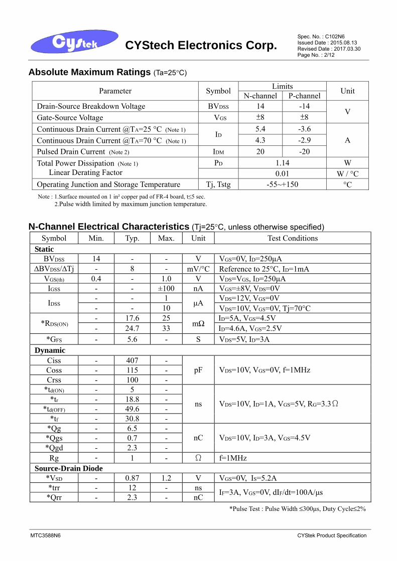
Absolute Maximum Ratings (Ta=25°C) Limits Parameter Symbol N-channel P-channel Unit
Drain-Source Breakdown Voltage BVDSS 14 -14 Gate-Source Voltage VGS ±8 ±8
V
Continuous Drain Current @TA=25 °C (Note 1) 5.4 -3.6 Continuous Drain Current @TA=70 °C (Note 1)
ID 4.3 -2.9
Pulsed Drain Current (Note 2) IDM 20 -20 A
PD 1.14 W Total Power Dissipation (Note 1) Linear Derating Factor 0.01 W / °C Operating Junction and Storage Temperature Tj, Tstg -55~+150 °C
Note : 1.Surface mounted on 1 in² copper pad of FR-4 board, t≤5 sec. 2.Pulse width limited by maximum junction temperature.
N-Channel Electrical Characteristics (Tj=25°C, unless otherwise specified) Symbol Min. Typ. Max. Unit Test Conditions
Static BVDSS 14 - - V VGS=0V, ID=250μA
∆BVDSS/∆Tj - 8 - mV/°C Reference to 25°C, ID=1mA VGS(th) 0.4 - 1.0 V VDS=VGS, ID=250μA IGSS - - ±100 nA VGS=±8V, VDS=0V
- - 1 VDS=12V, VGS=0V IDSS - - 10 μA VDS=10V, VGS=0V, Tj=70°C
- 17.6 25 ID=5A, VGS=4.5V *RDS(ON) - 24.7 33 mΩ ID=4.6A, VGS=2.5V *GFS - 5.6 - S VDS=5V, ID=3A
Dynamic Ciss - 407 - Coss - 115 - Crss - 100 -
pF VDS=10V, VGS=0V, f=1MHz
*td(ON) - 5 - *tr - 18.8 -
*td(OFF) - 49.6 - *tf - 30.8 -
ns VDS=10V, ID=1A, VGS=5V, RG=3.3Ω
*Qg - 6.5 - *Qgs - 0.7 - *Qgd - 2.3 -
nC VDS=10V, ID=3A, VGS=4.5V
Rg - 1 - Ω f=1MHz Source-Drain Diode
*VSD - 0.87 1.2 V VGS=0V, IS=5.2A *trr - 12 - ns *Qrr - 2.3 - nC IF=3A, VGS=0V, dIF/dt=100A/μs
*Pulse Test : Pulse Width ≤300μs, Duty Cycle≤2%

CYStech Electronics Corp.
Spec. No. : C102N6 Issued Date : 2015.08.13 Revised Date : 2017.03.30 Page No. : 3/12
MTC3588N6 CYStek Product Specification
P-Channel Electrical Characteristics (Tj=25°C, unless otherwise specified) Symbol Min. Typ. Max. Unit Test Conditions
Static BVDSS -14 - - V VGS=0V, ID=-250μA
∆BVDSS/∆Tj - -5 - mV/°C Reference to 25°C, ID=-1mA VGS(th) -0.4 - -1.0 V VDS=VGS, ID=-250μA IGSS - - ±100 nA VGS=±8V, VDS=0V
- - -1 VDS=-12V, VGS=0V IDSS - - -10 μA VDS=-10V, VGS=0, Tj=70°C
- 45.1 60 ID=-3.6A, VGS=-4.5V *RDS(ON) - 65.6 87 mΩ ID=-3.2A, VGS=-2.5V *GFS - 5.6 - S VDS=-5V, ID=-2A
Dynamic Ciss - 561 - Coss - 153 - Crss - 142 -
pF VDS=-10V, VGS=0V, f=1MHz
*td(ON) - 5 - *tr - 18.8 -
*td(OFF) - 49.6 - *tf - 30.8 -
ns VDS=-10V, ID=-1A, VGS=-5V, RG=3.3Ω
*Qg - 8 - *Qgs - 1 - *Qgd - 2.8 -
nC VDS=-10V, ID=-2A, VGS=-4.5V
Rg - 9.3 - Ω f=1MHz Source-Drain Diode
*VSD - -0.9 -1.2 V VGS=0V, IS=-3.4A *trr - 27 - ns *Qrr - 7 - nC IF=-2A, VGS=0V, dIF/dt=100A/μs
*Pulse Test : Pulse Width ≤300μs, Duty Cycle≤2% Thermal Data Parameter Symbol Value Unit Thermal Resistance, Junction-to-case, max RθJC 80 Thermal Resistance, Junction-to-ambient, max RθJA 110 (Note ) °C/W
Note :.Surface mounted on 1 in² copper pad of FR-4 board, t≤5 sec; 180°C/W when mounted on minimum copper pad
CYStech Electronics Corp.
Spec. No. : C102N6 Issued Date : 2015.08.13 Revised Date : 2017.03.30 Page No. : 4/12
MTC3588N6 CYStek Product Specification
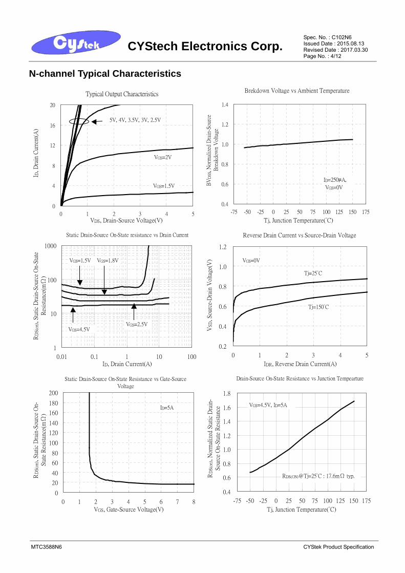
N-channel Typical Characteristics
Typical Output Characteristics
0
4
8
12
16
20
0 1 2 3 4 5VDS, Drain-Source Voltage(V)
I D, D
rain
Cur
rent
(A)
VGS=1.5V
VGS=2V
5V, 4V, 3.5V, 3V, 2.5V
Brekdown Voltage vs Ambient Temperature
0.4
0.6
0.8
1.0
1.2
1.4
-75 -50 -25 0 25 50 75 100 125 150 175
Tj, Junction Temperature(°C)
BV
DS
S, N
orm
aliz
ed D
rain
-Sou
rce
Bre
akdo
wn
Vol
tage
ID=250μA,
VGS=0V
Static Drain-Source On-State resistance vs Drain Current
1
10
100
1000
0.01 0.1 1 10 100ID, Drain Current(A)
RD
S(o
n), S
tati
c D
rain
-Sou
rce
On-
Sta
teR
esis
tanc
e(m
Ω)
VGS=1.8VVGS=1.5V
VGS=4.5VVGS=2.5V
Reverse Drain Current vs Source-Drain Voltage
0.2
0.4
0.6
0.8
1.0
1.2
0 1 2 3 4 5
IDR, Reverse Drain Current(A)
VS
D, S
ourc
e-D
rain
Vol
tage
(V)
Tj=25°C
Tj=150°C
VGS=0V
Static Drain-Source On-State Resistance vs Gate-Source
Voltage
0
20
40
60
80
100
120
140
160
180
200
0 1 2 3 4 5 6 7 8VGS, Gate-Source Voltage(V)
RD
S(o
n), S
tati
c D
rain
-Sou
rce
On-
Sta
te R
esis
tanc
e(m
Ω)
ID=5A
Drain-Source On-State Resistance vs Junction Tempearture
0.4
0.6
0.8
1.0
1.2
1.4
1.6
1.8
-75 -50 -25 0 25 50 75 100 125 150 175
Tj, Junction Temperature(°C)
RD
S(o
n), N
orm
aliz
ed S
tati
c D
rain
-S
ourc
e O
n-S
tate
Res
ista
nce VGS=4.5V, ID=5A
RDS(ON)@Tj=25°C : 17.6mΩ typ.
CYStech Electronics Corp.
Spec. No. : C102N6 Issued Date : 2015.08.13 Revised Date : 2017.03.30 Page No. : 5/12
MTC3588N6 CYStek Product Specification
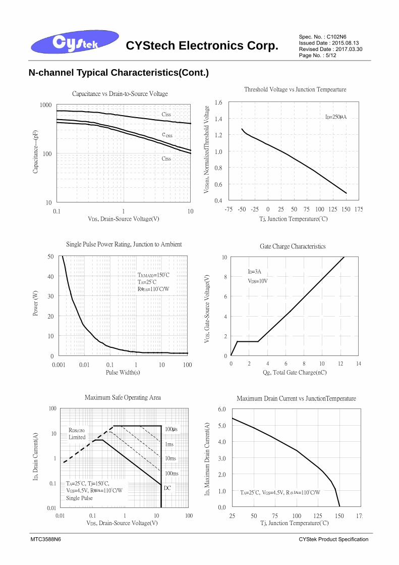
N-channel Typical Characteristics(Cont.)
Capacitance vs Drain-to-Source Voltage
10
100
1000
0.1 1 10VDS, Drain-Source Voltage(V)
Cap
acit
ance
---(
pF)
Coss
Ciss
Crss
Threshold Voltage vs Junction Tempearture
0.4
0.6
0.8
1.0
1.2
1.4
1.6
-75 -50 -25 0 25 50 75 100 125 150 175
Tj, Junction Temperature(°C)
VG
S(t
h), N
orm
aliz
edT
hres
hold
Vol
tage
ID=250μA
Single Pulse Power Rating, Junction to Ambient
0
10
20
30
40
50
0.001 0.01 0.1 1 10 100
Pulse Width(s)
Pow
er (
W)
TJ(MAX)=150°C
TA=25°C
RθJA=110°C/W
Gate Charge Characteristics
0
2
4
6
8
10
0 2 4 6 8 10 12 14
Qg, Total Gate Charge(nC)
VG
S, G
ate-
Sou
rce
Vol
tage
(V)
ID=3A
VDS=10V
Maximum Safe Operating Area
0.01
0.1
1
10
100
0.01 0.1 1 10 100
VDS, Drain-Source Voltage(V)
I D, D
rain
Cur
rent
(A)
DC
10ms
100ms
1ms
100μs
TA=25°C, Tj=150°C,
VGS=4.5V, RθJA=110°C/W
Single Pulse
RDS(ON)
Limited
Maximum Drain Current vs JunctionTemperature
0.0
1.0
2.0
3.0
4.0
5.0
6.0
25 50 75 100 125 150 175Tj, Junction Temperature(°C)
I D, M
axim
um D
rain
Cur
rent
(A)
TA=25°C, VGS=4.5V, RθJA=110°C/W
CYStech Electronics Corp.
Spec. No. : C102N6 Issued Date : 2015.08.13 Revised Date : 2017.03.30 Page No. : 6/12
MTC3588N6 CYStek Product Specification
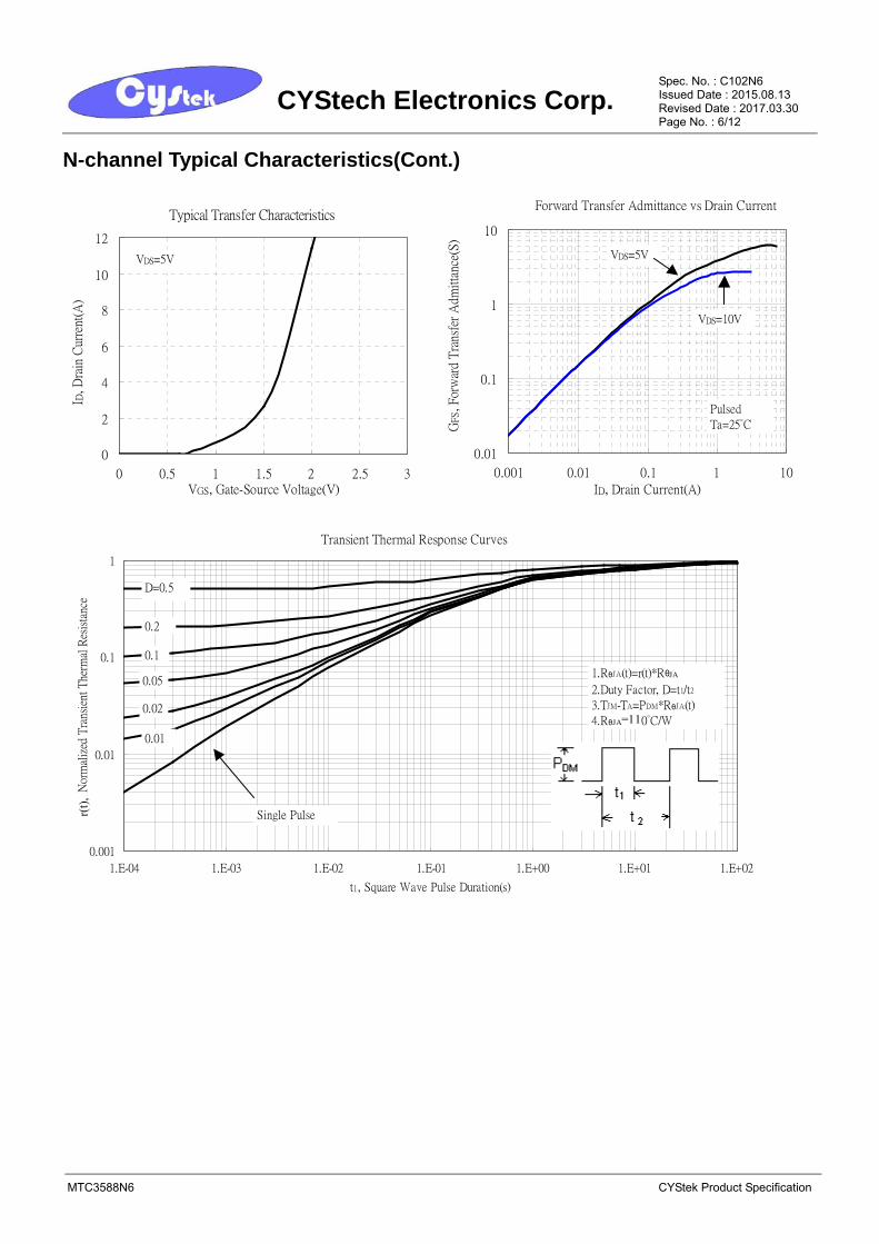
N-channel Typical Characteristics(Cont.)
Typical Transfer Characteristics
0
2
4
6
8
10
12
0 0.5 1 1.5 2 2.5 3VGS, Gate-Source Voltage(V)
I D, D
rain
Cur
rent
(A)
VDS=5V
Forward Transfer Admittance vs Drain Current
0.01
0.1
1
10
0.001 0.01 0.1 1 10
ID, Drain Current(A)
GF
S, F
orw
ard
Tra
nsfe
r A
dmit
tanc
e(S
)
Pulsed
Ta=25°C
VDS=10V
VDS=5V
Transient Thermal Response Curves
0.001
0.01
0.1
1
1.E-04 1.E-03 1.E-02 1.E-01 1.E+00 1.E+01 1.E+02
t1, Square Wave Pulse Duration(s)
r(t),
Nor
mal
ized
Tra
nsie
nt T
herm
al R
esis
tanc
e
Single Pulse
0.01
0.02
0.05
0.1
0.2
D=0.5
1.RθJA(t)=r(t)*RθJA
2.Duty Factor, D=t1/t2
3.TJM-TA=PDM*RθJA(t)
4.RθJA=110°C/W
CYStech Electronics Corp.
Spec. No. : C102N6 Issued Date : 2015.08.13 Revised Date : 2017.03.30 Page No. : 7/12
MTC3588N6 CYStek Product Specification
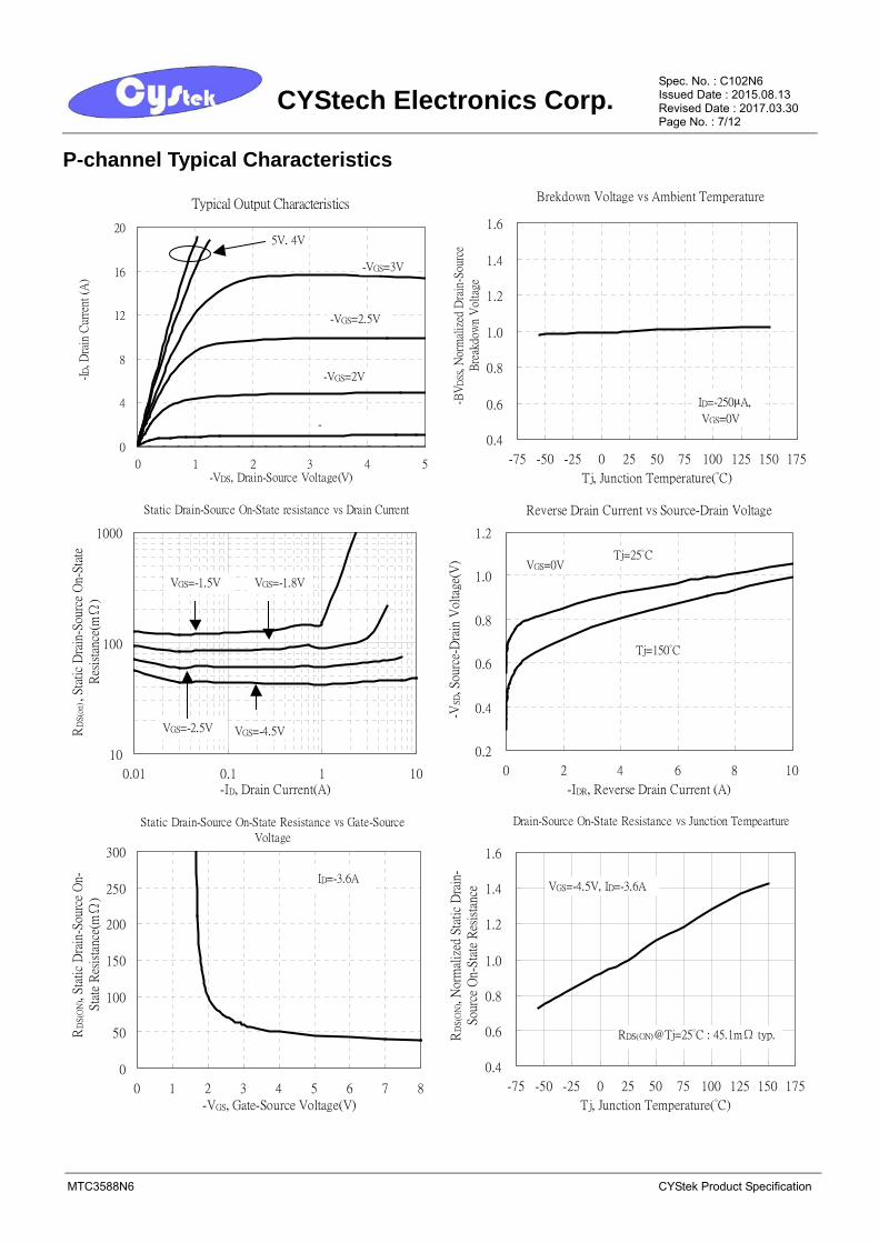
P-channel Typical Characteristics
Typical Output Characteristics
0
4
8
12
16
20
0 1 2 3 4 5-VDS, Drain-Source Voltage(V)
-ID, D
rain
Cur
rent
(A
)
-VGS=2.5V
-VGS=2V
-VGS=3V
5V, 4V
-
Brekdown Voltage vs Ambient Temperature
0.4
0.6
0.8
1.0
1.2
1.4
1.6
-75 -50 -25 0 25 50 75 100 125 150 175
Tj, Junction Temperature(°C)
-BV
DS
S, N
orm
aliz
ed D
rain
-Sou
rce
Bre
akdo
wn
Vol
tage
ID=-250μA,
VGS=0V
Static Drain-Source On-State resistance vs Drain Current
10
100
1000
0.01 0.1 1 10-ID, Drain Current(A)
RD
S(o
n), S
tati
c D
rain
-Sou
rce
On-
Sta
teR
esis
tanc
e(m
Ω)
VGS=-1.8VVGS=-1.5V
VGS=-2.5V VGS=-4.5V
Reverse Drain Current vs Source-Drain Voltage
0.2
0.4
0.6
0.8
1.0
1.2
0 2 4 6 8 1
-IDR, Reverse Drain Current (A)
-VS
D, S
ourc
e-D
rain
Vol
tage
(V)
0
Tj=25°C
Tj=150°C
VGS=0V
Static Drain-Source On-State Resistance vs Gate-Source
Voltage
0
50
100
150
200
250
300
0 1 2 3 4 5 6 7 8-VGS, Gate-Source Voltage(V)
RD
S(O
N),
Sta
tic
Dra
in-S
ourc
e O
n-S
tate
Res
ista
nce(
mΩ
)
ID=-3.6A
Drain-Source On-State Resistance vs Junction Tempearture
0.4
0.6
0.8
1.0
1.2
1.4
1.6
-75 -50 -25 0 25 50 75 100 125 150 175
Tj, Junction Temperature(°C)
RD
S(O
N),
Nor
mal
ized
Sta
tic
Dra
in-
Sou
rce
On-
Sta
te R
esis
tanc
e VGS=-4.5V, ID=-3.6A
RDS(ON)@Tj=25°C : 45.1mΩ typ.

CYStech Electronics Corp.
Spec. No. : C102N6 Issued Date : 2015.08.13 Revised Date : 2017.03.30 Page No. : 8/12
MTC3588N6 CYStek Product Specification
P-channel Typical Characteristics(Cont.) Capacitance vs Drain-to-Source Voltage
100
1000
0.1 1 10-VDS, Drain-Source Voltage(V)
Cap
acit
ance
---(
pF)
Coss
Ciss
Crss
Threshold Voltage vs Junction Tempearture
0.4
0.6
0.8
1.0
1.2
1.4
-75 -50 -25 0 25 50 75 100 125 150 175
Tj, Junction Temperature(°C)
-VG
S(t
h),N
orm
aliz
ed T
hres
hold
Vol
tage
ID=-250μA
Single Pulse Power Rating, Junction to Ambient
0
10
20
30
40
50
0.001 0.01 0.1 1 10 100Pulse Width(s)
Pow
er (
W)
TJ(MAX)=150°C
TA=25°C
RθJA=110°C/W
Gate Charge Characteristics
0
2
4
6
8
10
0 2 4 6 8 10 12 14 16
Qg, Total Gate Charge(nC)
-VG
S, G
ate-
Sou
rce
Vol
tage
(V)
VDS=-10V
ID=-2A
Maximum Safe Operating Area
0.01
0.1
1
10
100
0.01 0.1 1 10 100-VDS, Drain-Source Voltage(V)
-ID, D
rain
Cur
rent
(A
)
DC
10ms
100m
1ms
100μs
RDS(ON)
Limited
TA=25°C, Tj=150°C,
VGS=-4.5V, RθJA=110°C/W
Single Pulse
Maximum Drain Current vs JunctionTemperature
0.0
0.5
1.0
1.5
2.0
2.5
3.0
3.5
4.0
25 50 75 100 125 150 175Tj, Junction Temperature(°C)
-ID, M
axim
um D
rain
Cur
rent
(A)
TA=25°C, VGS=-4.5V, RθJA=110°C/W
CYStech Electronics Corp.
Spec. No. : C102N6 Issued Date : 2015.08.13 Revised Date : 2017.03.30 Page No. : 9/12
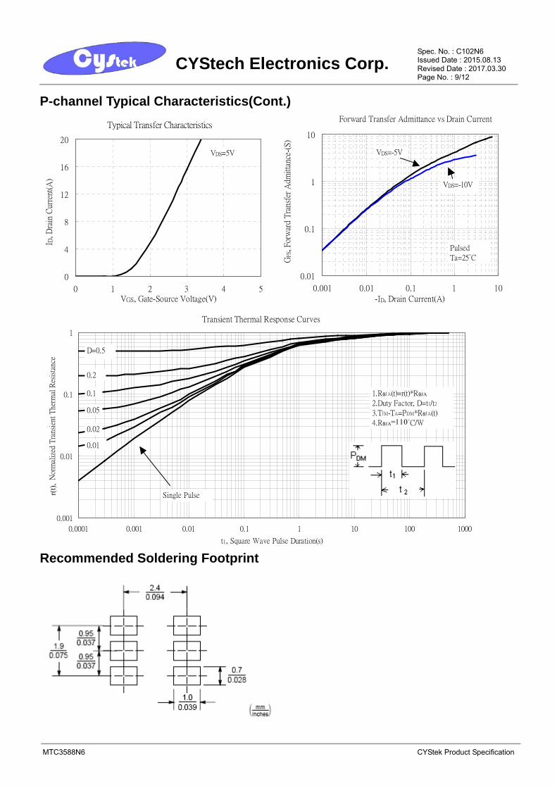
MTC3588N6 CYStek Product Specification
P-channel Typical Characteristics(Cont.) Typical Transfer Characteristics
0
4
8
12
16
20
0 1 2 3 4 5VGS, Gate-Source Voltage(V)
I D, D
rain
Cur
rent
(A)
VDS=5V
Forward Transfer Admittance vs Drain Current
0.01
0.1
1
10
0.001 0.01 0.1 1 10
-ID, Drain Current(A)
GF
S, F
orw
ard
Tra
nsfe
r A
dmit
tanc
e-(S
)
Pulsed
Ta=25°C
VDS=-10V
VDS=-5V
Transient Thermal Response Curves
0.001
0.01
0.1
1
0.0001 0.001 0.01 0.1 1 10 100 1000
t1, Square Wave Pulse Duration(s)
r(t),
Nor
mal
ized
Tra
nsie
nt T
herm
al R
esis
tanc
e
Single Pulse
0.01
0.02
0.05
0.1
0.2
D=0.5
1.RθJA(t)=r(t)*RθJA
2.Duty Factor, D=t1/t2
3.TJM-TA=PDM*RθJA(t)
4.RθJA=110°C/W
Recommended Soldering Footprint
CYStech Electronics Corp.
Spec. No. : C102N6 Issued Date : 2015.08.13 Revised Date : 2017.03.30 Page No. : 10/12
MTC3588N6 CYStek Product Specification
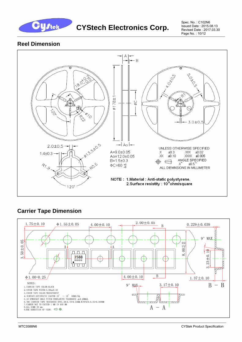
Reel Dimension
Carrier Tape Dimension
CYStech Electronics Corp.
Spec. No. : C102N6 Issued Date : 2015.08.13 Revised Date : 2017.03.30 Page No. : 11/12
MTC3588N6 CYStek Product Specification
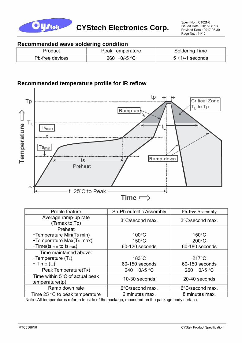
Recommended wave soldering condition Product Peak Temperature Soldering Time
Pb-free devices 260 +0/-5 °C 5 +1/-1 seconds Recommended temperature profile for IR reflow
Profile feature Sn-Pb eutectic Assembly Pb-free Assembly Average ramp-up rate
(Tsmax to Tp) 3°C/second max. 3°C/second max.
Preheat −Temperature Min(TS min) −Temperature Max(TS max) −Time(ts min to ts max)
100°C 150°C
60-120 seconds
150°C 200°C
60-180 seconds Time maintained above:
−Temperature (TL) − Time (tL)
183°C
60-150 seconds
217°C
60-150 seconds Peak Temperature(TP) 240 +0/-5 °C 260 +0/-5 °C
Time within 5°C of actual peak temperature(tp) 10-30 seconds 20-40 seconds
Ramp down rate 6°C/second max. 6°C/second max. Time 25 °C to peak temperature 6 minutes max. 8 minutes max.
Note : All temperatures refer to topside of the package, measured on the package body surface.
CYStech Electronics Corp.
Spec. No. : C102N6 Issued Date : 2015.08.13 Revised Date : 2017.03.30 Page No. : 12/12
MTC3588N6 CYStek Product Specification
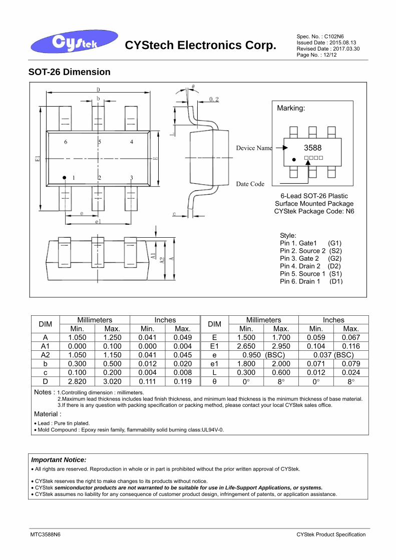
SOT-26 Dimension
Millimeters
Marking:
Inches Millimeters Inches DIM Min. Max. Min. Max. DIM Min. Max. Min. Max. A 1.050 1.250 0.041 0.049 E 1.500 1.700 0.059 0.067
A1 0.000 0.100 0.000 0.004 E1 2.650 2.950 0.104 0.116 A2 1.050 1.150 0.041 0.045 e 0.950 (BSC) 0.037 (BSC) b 0.300 0.500 0.012 0.020 e1 1.800 2.000 0.071 0.079 c 0.100 0.200 0.004 0.008 L 0.300 0.600 0.012 0.024 D 2.820 3.020 0.111 0.119 θ 0° 8° 0° 8°
Notes : 1.Controlling dimension : millimeters. 2.Maximum lead thickness includes lead finish thickness, and minimum lead thickness is the minimum thickness of base material.3.If there is any question with packing specification or packing method, please contact your local CYStek sales office.
Material : • Lead : Pure tin plated. • Mold Compound : Epoxy resin family, flammability solid burning class:UL94V-0.
Important Notice: • All rights are reserved. Reproduction in whole or in part is prohibited without the prior written approval of CYStek.
• CYStek reserves the right to make changes to its products without notice. • CYStek semiconductor products are not warranted to be suitable for use in Life-Support Applications, or systems. • CYStek assumes no liability for any consequence of customer product design, infringement of patents, or application assistance.
6-Lead SOT-26 Plastic Surface Mounted PackageCYStek Package Code: N6
Style: Pin 1. Gate1 (G1)Pin 2. Source 2 (S2)Pin 3. Gate 2 (G2)Pin 4. Drain 2 (D2)Pin 5. Source 1 (S1)Pin 6. Drain 1 (D1)
3588 □□□□
Device Name
Date Code
●
●
6 5 4
2 3 1