murdoch research repositoryresearchrepository.murdoch.edu.au/id/eprint/32585/1/application... · as...
TRANSCRIPT

MURDOCH RESEARCH REPOSITORY
This is the author’s final version of the work, as accepted for publication following peer review but without the publisher’s layout or pagination.
The definitive version is available at :
http://dx.doi.org/10.1109/AUPEC.2014.6966533
Barbieri, F., Chandrasena, R.P.S., Shahnia, F., Rajakaruna, S. and Ghosh, A. (2014) Application notes and recommendations on using TMS320F28335 digital Signal Processor to control voltage source converters. In: Australasian Universities Power Engineering Conference (AUPEC) 2014, 28 Sept. - 1 Oct.
2014, Perth, W.A
http://researchrepository.murdoch.edu.a/32585/
Copyright: © 2014 IEEE It is posted here for your personal use. No further distribution is permitted.

Copyright © 2014 IEEE. Personal use of this material is permitted.
Permission from IEEE must be obtained for all other uses, in any
current or future media, including reprinting/republishing this
material for advertising or promotional purposes, creating new
collective works, for resale or redistribution to servers or lists, or
reuse of any copyrighted component of this work in other works.

Application Notes and Recommendations on using TMS320F28335 Digital Signal Processor to Control
Voltage Source Converters
Florian Barbieri, Ruwan P.S. Chandrasena, Farhad Shahnia, Sumedha Rajakaruna and Arindam Ghosh Electrical and Computer Engineering Department
Curtin University Perth, Australia
Abstract—This paper presents general recommendations on utilizing TMS320F28335 Digital Signal Controller (DSC) as the controller for Voltage Source Converters (VSC). First, a com-parison is provided on different DSCs that can be used for such applications and the reasons for selecting this specific Texas Instrument device are discussed. Later, the strategy for real-time algorithm developed in the DSC, also referred to as digital Signal Processor (DSP) is explained and its main features that are used for VSC control are described. Some new functions are developed and their characteristics and specifications are sum-marized. The paper also presents a discussion on the most prob-able difficulties when programming the DSC/DSP for VSC con-trol applications followed by some improvement methods pro-posed for tackling these difficulties. Index Terms—Digital Signal Processor (DSP), TMS320F28335, Voltage Source Converter (VSC).
I. INTRODUCTION
Voltage Source Converters (VSC) are utilized in numerous applications in electrical systems spanning across motor and drive applications, energy harvesting from renewable energy resources, power quality improvement purposes in the trans-mission and distribution lines to HVDC systems [1]. The VSCs are composed of fully controlled semiconductor switches such as Insulated Gate Bipolar Transistors (IGBT) or Metal Oxide Semiconductor Field Effect Transistors (MOSFET) as their main building blocks. Each switch needs to have proper protection, driver and snubber circuits. Fig. 1 shows the schematics of a single-phase and three-phase VSC. It is to be noted that to prevent short-circuiting the DC link, the switches in each leg of the VSC must operate comple-mentarily.
The turn on and turn off the switches in the VSC should be based on providing a desired voltage, current or power at the output of the VSC. Therefore, the switchings in the VSC needs a pre-designed controller. For different objectives, the VSC might have an open-loop or closed-loop control. Open-loop control systems are much easier to be developed and hence are more popular. However, the closed-loop control systems provide a high improvement in the dynamic perfor-mance of VSCs. The closed-loop control systems can utilize different control strategies such as state-space, predictive, adaptive, non-linear, robust and optimal controls [2-3]. For a
Fig. 1. Schematic of a VSC: (a) Single-phase, (b) Three-phase.
Opto‐ coupler interface
Signal conditioning
DSP Board
Output
VSC + FilterDC
Link
Voltage and current
transducers
Fig. 2. Schematic of a VSC along with its closed-loop control system.
closed-loop control of a VSC, the desired voltage, current or power parameters at the output of the VSC should be moni-tored in real-time using proper sensors. The analogue outputs of the sensors should be first digitalized and then fed to the pre-designed controller. The controller should then define the proper turning on and turning off times of the switches and should export that information as commands in digital format to the driver circuits of the switches in the VSC through proper electrical isolation (i.e. by using opto-couplers). Fig. 2 shows a schematic diagram of a VSC along with its closed-loop control system.
The performance of VSCs highly depends on their control-lers. This performance can significantly improve if digital controllers are used. There are various options for implement-ing digital controls for VSCs. Microcontroller Units (MCU), Digital Signal Controllers (DSC), Digital Signal Processors (DSP) and Field Programmable Arrays (FPGA) are the most common options. DSCs can also be referred to as DSPs since their processor unit is a DSP. MCUs which their core is not a DSP, but a microprocessor, are not designed to operate in real-time applications [4]. Although they can be used for con
Australasian Universities Power Engineering Conference, AUPEC 2014, Curtin University, Perth, Australia, 28 September – 1 October 2014 1

Table 1.Comparison of different TI C2000 series, TMS320F28xxDSPs
Type DSP Model
Frequency (MHz)
RAM (kB)
Flash (kB)
ADC DAC No.
Price (US$) in 2014 No. Resolution (bit) Speed (ns)
Floating point
377D 200 204 1024 4 12/16 286 3 18.18 376D 200 172 512 4 12/16 286 3 15.93 335 150 68 512 1 12 80 0 14.25 334 150 68 256 1 12 80 0 14.05 332 100 52 128 1 12 80 0 13.20
Fixed point 12 150 36 256 1 12 80 0 14.25
Trolling VSCs, they will not result in very fast dynamic per-formances. FPGAs are slightly cheaper and can process data faster than DSPs. However, they need a much lower pro-gramming level compared to them. A comparison between DSP and FPGA for VSCs is presented in [5] and concludes that the FPGAs cost more than DSPs in terms of development time while resulting in almost similar dynamic results by the VSCs.
Nowadays, there are plenty of DSPs available in the mar-ket from different manufacturers with various specifications. Hence, the possible options should be carefully analyzed be-fore choosing a DSP. Among various DSP manufacturers, in 2006 it was reported that Texas Instruments® (TI) dominates the market by 59% [4]. Table 1 summarizes some of the TI processors in C2000 family, which are used for real-time ap-plications [6-7].It is to be noted that their ARM, C5000 and C6000 series are also applicable for real-time applications but are more commonly used for control applications requiring higher computations and data processing like multimedia or communication applications [4].
Depending on the application of the VSCs to be controlled, the DSP should have a specific number of Analogue-to-Digital Converters (ADC) and Digital-to-Analogue Conver-ters (DAC). In addition, depending on the number of calcula-tions to be carried out by the controller, the DSP should have a reasonable clock speed. It is to be noted that some DSPs have floating point support to provide high precision calcula-tions, whereas fixed point DSPs have a lower precision [4].
Among the C2000 series of TI, TMS320F28335 DSC/DSP is a better trade-off between price, performance and features [6, 7]. Hence, this specific DSP is one of the most popular DSPs used to control the VSCs. Unlike FPGAs and like other DSCs/DSPs, TMS320F28335 is a software based processor, built on a modified Harvard architecture. In addition, it can be programmed for real-time applications using C/C++ lan-guage. It is to be noted that this DSP lacks DACs; however, this is not normally required in VSC applications. In case a digital signal inside the DSP needs to be exported out in ana-logue format, some auxiliary DAC chips are available to be interconnected with the DSP. Alternatively, to export internal data in digital format to an external display, the data can be retrieved through a serial peripheral interface [8].
As a matter of comparison, the TMS320F2812 is also a popular DSC/DSP of the TI C2000 series. However, as an older fixed point unit model, its capability for numerical cal-culations of floating point data is more limited than that of the floating point DSC/DSPs [4, 6-7]. Additionally, for the same price of TMS320F28335, the TMS320F2812 offers slightly less interesting hardware resources, as listed in Table 1.
Fig. 3. (a) Packaged DSP, (b) TI DSP Experimenter’s Kit, (c) eZdspTM board, (d) Schematic of the DSP docking station.
II. DSP KITS AND DEVELOPMENT SOFTWARE
TMS320F28335 DSP comes either in a packaged chip or on a control card. In either of the above cases, the DSP needs to be mounted on a board. TI provides cheaper boards, re-ferred to as Experimenter’s Kit [9] where the control cards can be mounted on. More professional and expensive boards are also available for the packaged chips such as the Spec-trum Digital® eZdspTM board [10], which is one the most popular boards used for power electronic applications. Fig. 3 shows the TMS320F28335 DSP package chip along with its Experimenter’s Kit and eZdspTM board.
In general, a DSP docking station can be represented with the main modules shown in Fig. 3(d). The signals applied to the docking station are transmitted to and processed by the DSP processor and then retrieved from it. Input signals are applied on pins present on the docking station. These pins are internally connected to the General Purpose Input/Outputs (GPIO) of the DSP [6]. GPIOs can be set up by the user ei-ther as inputs or outputs. TMS320F28335 has 88 GPIOs that are connected to multiplexers. These multiplexers transmit multiplexed signals to sample-and-hold registers where the signals are held until the next conversion of the integrated ADC. The ADC outputs are then transferred to the processor of the DSP through the result registers of the ADC. In order to process the data, the code with which the DSP runs, can be loaded from the Flash memory or from the Static Random Access Memory (SRAM). The flash memory is utilized in stand-alone applications of the DSP while SRAM is utilized when the DSP is connected to its dedicated software on a computer. The outputs of the program are then exported via output GPIOs.
There are two possibilities to program the DSP. It can be programmed in C/C++language using Code Composer Studio (CCS) which is a dedicated software, developed by the manu-facturer [11]. This process requires a good level of C lan-
Australasian Universities Power Engineering Conference, AUPEC 2014, Curtin University, Perth, Australia, 28 September – 1 October 2014 2

guage knowledge as well as familiarity with the architecture of the DSP (e.g. its ADCs, Timers and GPIOs). Alternatively, the DSP can be programmed using MATLAB/SIMULINK® toolboxes. For this process, three extra toolboxes of MAT-LAB coder, SIMULINK coder and Embedded coder are re-quired to be utilized. However, this method provides an op-tion of utilizing majority of the built-in functions of MAT-LAB and programming the DSP with minimum knowledge of its architecture and the C language. Therefore, the latter is a better solution for users without a sound knowledge of C.
CCS is a tool to create real-time C projects, load them on the DSP. CCS also executes and debugs projects [12]. It con-tains an editor, a compiler and a debugger. The editor is used to compose the program, the compiler converts the C lan-guage-based code into assembly language and then to load the generated assembly code into the DSP. Then, the debug-ger is used to monitor the state of the parameters in the pro-gram during the execution period. The program can be ex-ecuted on stand-alone mode in the DSP; however, the DSP docking station should be connected to CCS in order to use the features of the debugger. It is to be noted that CCS cannot simulate any program and contains neither simulators nor models. CCS has a variety of built-in, structure-based, func-tions suitable for data/signal processing. However, all these functions may not be easy to be utilized nor optimized in terms of execution times, when compared with the needed functionality. The best solution in such cases is to develop custom functions. This can be very helpful when program-ming DSPs for VSCs. It is also to be noted that some of the built-in functions are specifically designed for fixed-point or particular DSPs. Hence, when utilizing such built-in functions proper modifications should be carried out to adapt them for the TMS320F28335 DSPs.
III. REAL-TIME ALGORITHM IN THE DSP
For real-time application, the developed algorithm inside the DSP is based on the principle of interruptions. TMS320F28335 DSP includes a set of three timers. However, only one timer, Timer0, can be utilized in the program. The Interruption Service Request (ISR) of Timer0 is used as the main clock for the program. The ISR is a C function, inde-pendent of the main function in the DSP algorithm. It needs to be declared and defined separately and is executed on the basis of regular interruptions of Timer0. The periods of the interruptions for Timer0 can be defined by the user for any value greater than 1 µs. The period of interruptions is utilized as the sampling period of the DSP program. As an example, considering the maximum switching frequency of the IGBTs as 20 kHz, the sampling period of the DSP program must be between 50 and 100 µs.
In order to ensure the real-time operation of the program, the total execution time of the ISR must be shorter than the sampling period. Therefore, variable definition, array initiali-zations as well as any calculations that do not need any real time input should be executed in the main function. Doing so helps to make the ISR very fast. Additionally, by using const-
Fig. 4. Structure schematic of the real-time program in the DSP.
ant values for indexing the arrays or by using constant values in calculations instead of variables the execution time of the program can be reduced significantly. Furthermore, calling an external function slows down the execution and should be avoided within the ISR. This is highly important regarding executing short and simple codes. It is to be noted that using macro definitions is useful when structures or built-in func-tions are used within the program
Finally, it must be noted that the main function needs to end with an infinite loop of type while(1);that does nothing but waits indefinitely until an interruption happens. After an interruption, the program leaves the main function and jumps to the ISR function related to the interruption. After the ISR is fully executed, the program goes back to the infinite loop within the main function and resumes the infinite cycle until the next interruption [9]. This structure is shown in Figure 4. It is to be highlighted that all the real-time functionality of the program is executed in the ISR of Timer0 and not in the main function. An example is provided at the end of Section IV to demonstrate the operation of the ISR.
IV. UTILIZED DSP PERIPHERALS
The analogue data from the sensors output is fed into the DSP program through the GPIOs in the DSP [6]. When run-ning the program in the DSP, the GPIOs should be set up as inputs or outputs by the help of an internal function. Then, the Analogue to Digital Converter (ADC) in the DSP is used to retrieve data. It is to be noted that the sample-and-hold circuit passes the data from the GPIOs to the ADC at specific inter-vals (e.g. in 12.5 MHz) in a fast sequential mode, with con-version performed at every ADC interruption. It is to be noted that the ADC has its own ISR. The period of interruptions depends on the ADC conversion frequency. Since the ADC conversion frequency is faster than the interruption frequency of Timer0, the ADC interruptions have a higher priority than Timer0. It is important to make sure that the ADC ISR has been executed at least once before starting the execution of Timer0 ISR. There are 16 ADC channels in TMS320F28335, which read input voltages in the range of 0 to 3 V. Its resolu-tion is 12 bits which can represent 4096 values. From this, each step of an ADC channel is 0.732 mV. If a more accurate
Australasian Universities Power Engineering Conference, AUPEC 2014, Curtin University, Perth, Australia, 28 September – 1 October 2014 3

ADC is required, an external ADC chip with higher resolu-tion can be utilized.
Since the ADC cannot read any input voltage greater than 3 V and does not support any negative voltages, the input signal needs to be adjusted before being applied to the ADC. This is done by adding an offset and then scaling the input signal in the range of 3 V. An operational amplifier-based circuit is used for this purpose. This data processing is shown as “Signal Processing” block in Fig. 2. Any offset or scaling carried out before the ADC should be converted back within the program to represent the original input voltage. As an example, considering a sinusoidal voltage with a magnitude of 10 V at the output of the sensor, the signal fed to the ADC and the signal within the DSP program are as shown in Fig. 5.
The ADC should be initialized by using built-in functions, available in TI Control Suite. It is necessary to define on what GPIOs the input signal is connected to. The ADC output data can be retrieved from the register AdcMirror. It must be re-minded that the result of the conversion is a code which for-mat depends on the resolution of the ADC. A further conver-sion using an appropriate ratio is thus necessary if the user wants to process in the program the real value of the physical quantity that was measured. Considering D as the decimal output of the ADC, the input voltage is equal to
−−+ +
−
−= ref
refref VVV
DV1212 (1)
in the DSP program where Vref+ = 3 V and Vref– = 0 V.
V. DEVELOPED & UTILIZED FUNCTIONS IN DSP PROGRAM
A limited number of functions are required to program a DSP for VSC applications. TI has a list of different built-in functions. However, as discussed earlier, to optimize the ex-ecution time of the program, some functions need to be de-veloped and tested independently within single independent projects. This approach can be beneficial in a very early stage of discovery to get familiar with the development environ-ment and comparing them with the built-in functions.
To make the programming simpler and more time-efficient, it is recommended to develop a project by using the following method: 1- First, a flow chart of the complete algorithm of the pro-
gram should be drawn with a description of each function. 2- Only one single function should be implemented and tested
at each stage. 3- Once the first version of the project is tested successfully,
the main .c file may be duplicated and renamed within the same project.
4- The old file needs to be excluded from the project and re-placed by its duplicate in which an additional function will be added and tested.
A. Sine Wave Generating Function A sine wave generating function is developed and imple-
mented in the main function, in order to relieve the Timer0 ISR. This function consists of a ‘for loop’ filling in each ele-ment of an array with its sine function value. In order to as-sign time-respective sine values in the array at each sampling
Fig. 5. The sampled signal before and after the ADC and within the ISR.
time, the local variable ‘TIME’ is used as the time variable in the form of
)2sin(.][_sin_);_;0(
sTTIMEfMTIMEwaveeGeneratedTIMEsizearrayTIMETIMEfor
××=++<=
π
where M is the desired magnitude for the generated sine wave, f is its frequency and Ts is the sampling period of the DSP program. The math.h header requires to be included in the pre-processing section of the program. The size ar-ray_size is fixed according to f and Ts from
sTfsizearray
.1_ = (2)
As an example, to generate a reference voltage with f = 50 Hz and a sampling time of Ts = 80µs, the size of array_size is calculated as 20ms / 80µs = 250 elements.
Even though it is strongly recommended not to use any ‘for loop’ or to make complex calculations in real-time pro-grams, the ‘for loop’ utilized in this function does not lead to any delay in the real-time execution of the program. This is because this function is developed outside the TIMER0 ISR. It is to be noted that if a sine wave generating block is re-quired to be built within the ISR, a lookup table option is definitely better from time execution point of view. B. High Pass Filter
As discussed earlier, the signals digitally converted by the ADC have a DC offset value. To eliminate this DC offset of the input signals or to extract the high frequency components from any desired signal, a High Pass Filter (HPF) needs to be developed and utilized within the ISR. Even though TI Con-trol Suite has some built-in Infinite Impulse Response (IIR) and Finite Impulse Response (FIR) digital filters available in its libraries, such functions can be too complex to use as well as too much time-consuming to run. It is simpler to develop a more optimized digital IIR filter based on the conversion of the transfer function of the filter. A first order HPF in z-domain is expressed as
11
110.1
.)( −
−
+
+=
zb
zaazH (3)
whereω210 +
==s
sT
Taa and ωω
22
1 +−=
ss
TTb and ω is the desired cut-
off angular frequency of the filter. From (3), the output of the HPF developed in ISR is ex-pressed based on its inputs as
)(.)(.)(.)( 110 ss TTIMEybTTIMExaTIMExaTIMEy −−−+= (4)
where x and y are respective the input and output of the HPF. The equation (4) needs to be implemented with two sets of circular buffers, each consisted of two-element– one set for the input values and one set for the output values. The circu-lar buffer operates as discussed below:
At the first execution of the ISR (i.e. TIME = 0), the input V1 is saved as the first element of the buffer. At the second
Australasian Universities Power Engineering Conference, AUPEC 2014, Curtin University, Perth, Australia, 28 September – 1 October 2014 4

execution of the ISR (i.e. TIME = Ts), the input is saved as the second element of the buffer. From the third execution of the ISR onwards (e.g. TIME = 2Ts, 3Ts, …), the first element of the buffer is overwritten by the second element while a new input is saved as its second element. This is shown schematically in Fig. 6.
A similar methodology can be applied when implementing a low pass filter. C. Sine Wave Analyzer
Different methods can be utilized to define the magnitude and phase angle of a given signal, as discussed below: 1- Using the Fast Fourier Transform (FFT) the magnitude and
phase angle for different frequency components can be calculated. However, due to high number of calculations it is not really suitable for real-time control of VSCs.
2- If only the magnitude and phase angle of one specific fre-quency (e.g. 50 Hz) is required to be utilized in ISR, then the Sine Analyzer and Digital Phase Locked Loop (PLL) built-in functions of TI Control Suite are more time-efficient.
3- If the input signals have frequencies other than constant 50 Hz (which is more probable in off-grid applications of VSCs), then a Discrete Fourier Transform (DFT) can be developed by the user and operate fast enough to be uti-lized for real-time purposes. The DFT first detects the fundamental frequency of the input signal and then calcu-lates its magnitude and phase angle.
The developed DFT calculates the root mean square (RMS) and phase angle of the fundamental frequency of its input signal, regardless of the signal frequency from
)/(tan
2
1
22
ABAngle
BAN
RMS
−=
+= (5)
where N is the number of samples within a period of the sig-nal (e.g. N=250 for a 50 Hz input signal), A is the sum of the real components of the input signal over one period, calcu-lated as
∑∑==
⎟⎠
⎞⎜⎝
⎛==N
i
N
ii N
iixxA00
2cos.][)Re( π (6)
and B is the sum of the imaginary components of the input signal over one period
∑∑==
⎟⎠
⎞⎜⎝
⎛==N
i
N
ii N
iixxB00
2sin.][)Im( π (6)
It is to be noted that the angle needs to be in the range of [0- 2π]. Hence, mathematical function of atan2 should be utilized when developing (5) in ISR. The number of samples N is calculated by measuring the period of the input signal. To do so, the DC component of the input signal is filtered out and at least two periods of the filtered signal need to be stored in a large array. N is given by the number of elements in the large array between two zero-crossings of the signal.
Circular buffers containing N elements are used to calcu-late A and B. The principle of this method is similar to the procedure explained in the HPF section. Since the buffers are
Table 2. Comparison of execution times [clock cycles]. Input Signal FFT DFT Sine Analyzer + PLL 1-freq. Signal 17622 2063 375 2-freq. Signal 17622 2062 376 3-freq. Signal 17622 2056 376
1x 1x 1x 1x1v 2v1v0x 0x 0x 0x
2v 2v 2v 3v
1v 2v 3v2v
1x 1x0x 0x3v 3v
3v
4v3v
4v
Fig. 6. Schematic operation of a 2-element circular buffer.
bigger, the process differs slightly though, as discussed be-low: 1-During the N first executions of the ISR, the buffers A and
B are filled in with the calculated values. 2- At the end of the Nth execution of the ISR, the buffers are
full and the input RMS and angle are calculated. 3- At the beginning of the (N+1)th execution of the ISR and
onwards, the values of the oldest real element within the current input signal period is subtracted from A and the oldest imaginary element within the current input signal period is subtracted from B
4- Within the same execution cycle of the ISR, a new real element and a new imaginary element of the input signal are calculated and respectively added to A and B.
5- Within the same execution cycle of the ISR, the RMS am-plitude and phase angle are calculated and updated.
Comparing the above three methods, FFT has the longest computational delay while the Sine Analyzer and PLL com-bination has the least computational delay. As an example, Table 2 lists a comparison of the execution times, expressed in number of clock cycles, to process several different input signals. D. Deadband and Hysteresis Function To provide an acceptable level of tracking for the VSC cur-rent and voltage, the difference between the desired output and the actual output should be calculated. This is referred to as the VSC output tracking error, which should be kept close to zero. Hence, a hysteresis controller can be developed and utilized to properly turn on and turn off the switches in the VSC to keep the tracking error within a very small bandwidth around zero. This can be achieved by developing ‘if state-ments’ in the ISR. ‘If statements’ are very fast to execute and only creates a negligible delay. Depending on the output of the ‘if statements’ a couple of predefined output GPIOs are set to logic High or Low. The GPIOs being set as High or Low activates or deactivates the driver circuits of a switch to which the GPIO is connected.
As discussed earlier, the switches in each leg of the VSC should operate in a complimentary fashion to prevent short-circuiting the DC bus. Hence, it is necessary to implement a dead-band between the assignments of the complementary output GPIOs to guarantee the prevention of any probable short-circuits. The dead-band is created by using a ‘while loop’ and by incrementing a counter until a certain value cor-responding to the desired delay. The desired delay should be defined based on the recommended deadband of the switches.
Australasian Universities Power Engineering Conference, AUPEC 2014, Curtin University, Perth, Australia, 28 September – 1 October 2014 5
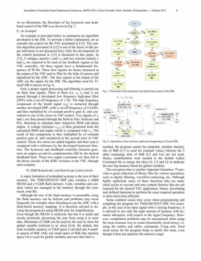
As an illustration, the flowchart of the hysteresis and dead-band control of the ISR is as shown in Fig. 7. E. An Example
An example is provided below to summarize an algorithm developed in the ISR. To provide a better explanation, let us consider the control for the VSC presented in [13]. The con-trol algorithm presented in [13] is not of the focus of this pa-per and hence is not discussed here. Only the development of the control presented in [13] is discussed in this paper. In [13], 2 voltages, namely vt and vcf, and two currents namely it and ish are required to be used as the feedback signals to the VSC controller. All these signals have a fundamental fre-quency of 50 Hz. These four signals are hence measured at the output of the VSC and its filter by the help of sensors and digitalized by the ADC. The four signals at the output of the ADC are the inputs for the ISR. The algorithm used for Ti-mer0 ISR is shown in Fig. 8.
First, a proper signal processing and filtering is carried out on these four signals. Three of them (i.e. vt, vcf and it) are passed through a developed low frequency high-pass filter (HPF) with a cut-off frequency of 1 Hz. The high frequency component of the fourth signal (ish) is extracted through another developed HPF, with a cut-off frequency of 2.4 kHz, and then multiplied by of constant positive gain K2 and con-sidered as one of the errors in VSC control. Two signals of vt and it are then passed through the built-in Sine Analyzer and PLL functions to calculate their respective RMS and phase angles. A voltage reference vcf,ref is then generated from the calculated RMS and angles which is compared with vcf. The result of this comparison is then multiplied by of constant positive gain K1 and considered as the second error in VSC control. These two errors are added together and their sum is compared with a reference by the developed hysteresis func-tion. The hysteresis and deadband controller function gene-rates an output out and its complementary by the desired deadband limit. These two output commands are then fed to the driver circuits of the IGBT switches in the VSC, through opto-couplers.
VI. DSP HARDWARE AND SOFTWARE LIMITATIONS
A major limitation of embedded systems is the size of their memory. The TMS320F28355 DSP only contains a 68kB SRAM and a 512kB flash memory. Code, variables and con-stant values are managed in the memory through the com-mand .cmd file.
Although the size of the flash memory is reasonable, using the flash memory can be delicate and problems may occur frequently for example when intending to run the ADC with a flash-based memory mapping. It is therefore advised to de-velop the program by using SRAM only for simplification. Even though the SRAM is relatively fast but it is small and mostly protected, preventing the user from using it to store data. Maximum of 32kB can be used by the user to store the global variable (referred to as .ebss) [4-6]. By default, this total available memory of 32kB space is divided into 4 small-er spaces of 8kB. Only one small space of 8kB (the memory space L4) is used for global variables and once that limit is
Fig. 7. Flowchart of the hysteresis and dead-band control of the ISR.
cfvtv ti shi
cfv ′tv′ ti ′
tvθtiθ
tv
ti
2K
refcfv ,1K
out
out
Fig. 8: Algorithm of the real-time application happening in Timer0 ISR.
reached, the program cannot be compiled. Another memory slot of 8kB (L7) is used for constant values whereas the 2 other remaining slots of 8kB (L5 and L6) are not used. Hence, modifications were needed in the default Linker Command file to merge the slots L4, L5 and L6 to dedicate the new big memory block for global variables.
The execution time is another important limitation; TI pro-vides a good collection of library files for various operations, such as digital filtering, waveform analyzing, etc. Although highly optimized, many of these functions take too many clock cycles to execute and may contain features that are not required for the desired VSC application. Hence, developing user defined functions to perform the exact required operation is often more time-efficient.
Some common issues may occur when programming and compiling the program for TMS320F28355 DSP. For exam-ple, in the case of an input signal with a varying frequency, it is advised to use only the right amount of memory with dy-namic allocation, with respect to the signal frequency. How-ever, compilation problems may be encountered when using the most common way to create dynamically sized arrays, i.e. using the malloc and calloc commands. Using only fixed sized arrays for the program helps to tackle this issue, even though it does not optimize the memory usage.
Australasian Universities Power Engineering Conference, AUPEC 2014, Curtin University, Perth, Australia, 28 September – 1 October 2014 6

Another common problem is the loss of connection be-tween the CCS and DSP docking station when high voltages are used in the surrounding environment [14]. This is due to the fact that a direct Joint Test Action Group (JTAG) connec-tion cannot cope with a too high amount of electrical noise. In such a case, the Future Technology Devices (FTDI) chip driver will crash and disrupt the communication. This prob-lem can be solved by using an isolated adapter for JTAG emulator such as TI TMDSADP1414-ISO [15] or Spectrum digital SPI110LV [16].
VII. MONITORING AND DEBUGGING DSP PROGRAM
TI CCS enables the user to optimize automatically a project during its compilation in terms of execution speed or the code size. Additionally, CCS provides real-time access to the DSP memory to monitor any variables during the execu-tion of the program, provided that CCS is in debugging mode and the host computer is connected to the target.
To display one full period of the waveform of a periodic signal generated internally or acquired through ADC in CCS, an array needs to be created. For a signal with a constant fre-quency, the created array Array[N] contains N elements so that it stores all the samples over one period. The calculation of the size of the array is as discussed in (2). For example, for a signal with a frequency of 50 Hz, N = 250. Then, an index pointer is created in order to point at the element of the array where the corresponding sample of the waveform needs to be saved. The index is an integer that is initialized to 0 and in-cremented during each interruption until it reaches the value N–1. It is then reset to 0 in order to start a new cycle such that each element of the array is overwritten by the same sample. For example, for a 50 Hz signal, the rest happens when the index pointer reaches 249. Now, if the program runs and the real-time debugger of CCS is enabled, the graph tool can be used to display the values of Array[N] which is stored in the memory from the address &Array[0] and onwards.
However, if the frequency of the signal is varying, the size of the array should also vary accordingly, or alternatively, the space used in the array should change in consequence, pro-vided the array is large enough to contain all the samples of the longest expected period. In this case, in an array of size n+1 (e.g. 400) containing the elements [a0 - an], only the ele-ments from [a0, a1, …, ak] are considered while the remaining elements [ak, ak+1, …, an] are ignored. k is determined from the signal period similar to (2). This measurement is updated at every Timer0 ISR interruption. The illustration of this strategy is shown on Fig. 9. Even though resource consum-ing, this method performs well and is simple to implement.
It must be noted that a mismatch between the number of elements displayed in the graph and the period of the wave-form may cause the waveform to look as if it was moving inside the graph, making the observations difficult.
Furthermore, setting break points within the program is a versatile tool provided by TI CCS to measure the execution time of certain instructions or sets of instructions, in terms of number of clock cycles. This function is available only when CCS is running in debugging mode with enabled clock tool.
1a 2a 3a ka na0a
Fig. 9. Dynamic use of a fixed-size array
For the program to perform in real-time, the execution time of the Timer0 ISR function needs to be measured and limited to less than the sampling period.
VIII. CONCLUSION
DSPs and in particular TI TMS320F28335 are powerful tools to implement digital control systems for a VSC. How-ever, the user must be experienced in C language program-ming and must understand the architecture of the DSP in or-der to be able to achieve the implementation of the control with CCS. Moreover, although TI has conveniently devel-oped a series of built-in functions, the user may need to modi-fy them or develop new custom functions to improve the ex-ecution time of the program.
REFERENCES [1] R. Feldman, M. Tomasini, E. Amankwah, et al. “A Hybrid Modular
Multilevel Voltage Source Converter for HVDC Power Transmission,” IEEE Trans. on Industry Applications, Vol. 49, No. 4, pp. 1577–1588, July/August 2013
[2] F. Huerta, S. Cóbreces, F. J. Rodríguez, et al. “State-Space Model Iden-tification of an LCL Filter used as interface between a Voltage Source Converter and the electrical grid,” in Proc. of IEEE Energy Conversion Congress and Exposition (ECCE), 2009
[3] R.M. Milasi, A.F. Lynch and Y.W. Li, “Adaptive vector control for voltage source converters,” IET Control Theory Appl., 2013, Vol. 7, Iss. 8, pp. 1110–1119
[4] F. Bormann, C2000™ Teaching CDROM– 3rd Rev. 2010 (available at: http://www.ti.com/europe/docs/univ/)
[5] C.A. Sepúlveda, J.A. Muñoz, J.R. Espinoza, et al. “FPGA v/s DSP Per-formance Comparison for a VSC-Based STATCOM Control Applica-tion,” IEEE Trans. on Industrial Informatics, Vol. 7, No. 2, pp. 1351–1360, May 2011
[6] TMS320F28335 Digital Signal Controllers (DSCs), Data Manual, Lite-rature Number: SPRS439M, June 2007–Revised August 2012, http://www.ti.com/lit/ds/sprs439m/sprs439m.pdf
[7] TMS320F2837xD, Dual-Core Delfino™ Microcontrollers, Literature Number: SPRS880A, December 2013–Rev. March 2014, Texas Instru-ments http://www.ti.com/lit/ds/symlink/tms320f28376d.pdf
[8] TMS320x2833x, 2823x Serial Communications Interface (SCI), Litera-ture Number: SPRUFZ5A August 2008–Revised July 2009 Texas In-struments http://www.ti.com/lit/ug/sprufz5a/sprufz5a.pdf
[9] Quick Start Guide, TMS320C2000™ Experimenter’s Kit Overview, Literature Number: SPRUFR5F, June 2008–Revised Feb. 2011, Texas Instruments, available at http://www.ti.com/lit/ml/sprufr5f/sprufr5f.pdf
[10] eZdspTM, F28335, Technical Reference 510195-0001, Nov. 2007, De-velopment Systems, Spectrum Digital Inc., available at http://c2000.spectrumdigital.com/ezf28335/docs/ezdspf28335c_techref.pdf
[11] Code Composer Studio (CCS) Website, http://www.ti.com/tool/ccstudio [12] C2000 Getting Started with Code Composer Studio v.5 Manual
http://processors.wiki.ti.com/index.php/C2000_Getting_Started_with_Code_Composer_Studio_v5
[13] F. Shahnia, R.P.S. Chandrasena, S. Rajakaruna, et al. “Primary control level of parallel distributed energy resources converters in system of multiple interconnected autonomous microgrids within self-healing net-works,” IET Gen., Trans. & Dist., Vol. 8, Issue 2, pp. 203-222, 2014.
[14] JTAG Emulator Adapter Board Kit 14e-60t Quick Start Guide, 2004, Texas Instruments http://www.ti.com/lit/ug/spru814/spru814.pdf
[15] Emulation and Trace Headers, Technical Reference Manual, Literature Number: SPRU655I. Feb. 2003–Revised Aug. 2012, Texas Instruments, available at http://www.ti.com/lit/ug/spru655i/spru655i.pdf
[16] http://www.spectrumdigital.com/product_info.php?products_id=33
Australasian Universities Power Engineering Conference, AUPEC 2014, Curtin University, Perth, Australia, 28 September – 1 October 2014 7