multiport ultra low-power ethernet switches
TRANSCRIPT

53106S-DS103-R
Corporate Headquarters: San Jose, CA September 12, 2016
Data Sheet
BCM53106S
Multiport Ultra Low-Power Ethernet SwitchesGENERAL DESCRIPTION FEATURES
The Broadcom® BCM53106S is an ultra low-power, highlyintegrated, cost-effective smart Fast Ethernet switch. Theswitch design is based on the field-proven, industry-leadingROBO architecture. This device combines all the functionsof a high-speed switch system including packet buffers,PHY transceivers, media access controllers (MACs),address management, port-based rate control, and anonblocking switch fabric into a single 28 nm CMOS device.Designed to be fully compliant with the IEEE 802.3 andIEEE 802.3x specifications, including the MAC-controlPAUSE frame, the BCM53106S provides compatibility withall industry-standard Ethernet and Fast Ethernet devices.
The BCM53106S has a rich feature set suitable for not onlystandard Fast Ethernet connectivity for broadband homegateways, desktop and laptop PCs, but also for next-generation gaming consoles, set-top boxes, networkedDVD players, and home theater receivers. It is alsospecifically designed for next generation SOHO/SMBrouters and gateways.
The BCM53106S contains four full-duplex 10/100BASE-TXEthernet transceivers. In addition, the BCM53106S has twoPHY-less interfaces for the CPU or a router chip, providingflexible 10/100 Mbps connectivity. One RGMII interface canbe connected to a CPU entity and configured as an IMP (InBand Management port).
The second RGMII interface is available for another PHY,Modem, or CPU connection.
The BCM53106S provides 70+ on-chip MIB counters tocollect receive and transmit statistics for each port.
The BCM53106S is available in industrial temperature (I-Temp) and commercial temperature (C-Temp) ratedpackages. The BCM53106S is available in one packagetype, a 212-pin FBGA package.
• Four 10/100M and two 10/100/1000M media accesscontrollers
• Four-port 10/100 transceivers for TX• One RGMII interface for an inband management port
(IMP) for connection to a CPU/management entitywithout PHY
• One RGMII interface for a connection to another PHY,CPU, or Modem.
• IEEE 802.1p, MAC Port, TOS, and DiffServ QoS for sixqueues, plus two time sensitive queues
• Port-based VLAN• IEEE 802.1Q-based VLAN with 4K entries• MAC-based trunking with automatic link failover• Port-based rate control• Port mirroring (Ingress/Egress)• Supports IPv4 and IPv6• Priority modification on egress• BroadSync® HD for IEEE 802.1AS support• Timestamp tagging at MAC interface• Time-aware egress scheduler• DOS attack prevention• IGMP Snooping, MLD snooping support• Spanning tree support (multiple spanning trees–up to
eight)• Embedded CPU (8051) processor for cable
diagnostics.• CableChecker™ with unmanaged mode support• Double tagging/QinQ• IEEE802.az Energy Efficient Ethernet (EEE) support• IEEE 802.3x programmable per-port flow control and
backpressure, with IEEE 802.1X support for secureuser authentication
• EEPROM, MDC/MDIO, and SPI Interface.• Serial Flash Interface for accessing embedded CPU
(8051)• 4K entry MAC address table with automatic learning
and aging• 128 KB packet buffer (1 KB = 1024 bytes)• 128 multicast group support• Jumbo frame support up to 9720 byte• 1.0V for core and 3.3V for I/O• RGMII with option of 2.5V or 1.5V• JTAG support• 212-pin FBGA package

Revision HistoryBCM53106S Data Sheet
Broadcom®
September 12, 2016 • 53106S-DS103-R Page 2BROADCOM CONFIDENTIAL
Figure 1: BCM53106S Functional Block Diagram
10/100 PHY
10/100 PHY
10/100 PHY
10/100 PHY
GMAC
GMAC
GMAC
GMAC
GMAC
GMAC
Registers
Packet Buffer MMU
Address
Management
LED Interface
8051 Micro
Controller
EEPROM/SPI
Interface
TDP/N_0_[1:0]
TDP/N_1_[1:0]
TDP/N_2_[1:0]
TDP/N_3_[1:0]
RGMII
RGMII
LED
Flash
Memory
EEPROM/
CPU

© 2016 by Broadcom. All rights reserved.
Broadcom®, the pulse logo, Connecting everything®, Avago Technologies, and the A logo are among thetrademarks of Broadcom and/or its affiliates in the United States, certain other countries and/or the EU. The
term “Broadcom” refers to Broadcom Limited and/or its subsidiaries. For more information, please visitwww.broadcom.com.
Broadcom reserves the right to make changes without further notice to any products or data herein to improvereliability, function, or design. Information furnished by Broadcom is believed to be accurate and reliable.
However, Broadcom does not assume any liability arising out of the application or use of this information, northe application or use of any product or circuit described herein, neither does it convey any license under its
patent rights nor the rights of others.
This data sheet (including, without limitation, the Broadcom component(s) identified herein) is not designed,intended, or certified for use in any military, nuclear, medical, mass transportation, aviation, navigations,
pollution control, hazardous substances management, or other high-risk application. BROADCOMPROVIDES THIS DATA SHEET “AS-IS,” WITHOUT WARRANTY OF ANY KIND. BROADCOM DISCLAIMS
ALL WARRANTIES, EXPRESSED AND IMPLIED, INCLUDING, WITHOUT LIMITATION, THE IMPLIEDWARRANTIES OF MERCHANTABILITY, FITNESS FOR A PARTICULAR PURPOSE, AND NON-
INFRINGEMENT.
Revision History
Revision Date Change Description
53106S-DS103-R 09/12/16 Updated:
• Table 29: “Pin Lit by Pin Number,” on page 115
53106S-DS102-R 08/12/16 Updated:
• Table 33: “Electrical Characteristics,” on page 13053106S-DS101-R 02/24/16 Updated:
• Table 33: “Signal Descriptions,” on page 12353106S-DS100-R 07/09/15 Initial release.

Table of ContentsBCM53106S Data Sheet
Broadcom®
September 12, 2016 • 53106S-DS103-R Page 4
BROADCOM CONFIDENTIAL
Table of Contents
About This Document ................................................................................................................................ 13
Purpose and Audience.......................................................................................................................... 13
Acronyms and Abbreviations................................................................................................................. 13
Document Conventions ......................................................................................................................... 13
References ............................................................................................................................................ 14
Technical Support ...................................................................................................................................... 14
Section 1: Introduction ..................................................................................................... 15
Overview...................................................................................................................................................... 15
Audience ..................................................................................................................................................... 16
Data Sheet Information .............................................................................................................................. 16
Section 2: Features and Operation .................................................................................. 17
Overview...................................................................................................................................................... 17
Quality of Service and Scheduling ........................................................................................................... 18
CoS Mapping......................................................................................................................................... 21
SF3 Egress Queues and Scheduler...................................................................................................... 21
Egress Transmit Queues ............................................................................................................... 21
Scheduler ....................................................................................................................................... 23
Scheduling............................................................................................................................................. 25
Leaky Bucket Shaper ............................................................................................................................ 26
Port-Based VLAN........................................................................................................................................ 27
IEEE 802.1Q VLAN...................................................................................................................................... 27
IEEE 802.1Q VLAN Table Organization................................................................................................ 28
Double-Tagging .......................................................................................................................................... 28
ISP Port ................................................................................................................................................. 29
Customer Port ....................................................................................................................................... 29
Uplink Traffic (from Customer Port to ISP)............................................................................................ 30
Downlink Traffic (from ISP to Customer Port) ....................................................................................... 30
Jumbo Frame Support ............................................................................................................................... 31
Port Trunking/Aggregation........................................................................................................................ 31
WAN Port..................................................................................................................................................... 32
Rate Control ................................................................................................................................................ 32
Ingress Rate Control ............................................................................................................................. 32
Two-Bucket System .............................................................................................................................. 33
Egress Rate Control .............................................................................................................................. 34
Bucket Bit Rate...................................................................................................................................... 34
Protected Ports........................................................................................................................................... 34

Table of ContentsBCM53106S Data Sheet
Broadcom®
September 12, 2016 • 53106S-DS103-R Page 5
BROADCOM CONFIDENTIAL
Port Mirroring.............................................................................................................................................. 35
Enabling Port Mirroring.......................................................................................................................... 35
Capture Port .......................................................................................................................................... 35
Mirror Filtering Rules ............................................................................................................................. 35
Port Mask Filter .............................................................................................................................. 35
Packet Address Filter ..................................................................................................................... 36
Packet Divider Filter ....................................................................................................................... 36
IGMP Snooping........................................................................................................................................... 36
MLD Snooping ............................................................................................................................................ 36
IEEE 802.1X Port-Based Security.............................................................................................................. 37
DoS Attack Prevention............................................................................................................................... 38
Multiple Spanning Tree Protocol .............................................................................................................. 39
Software Reset............................................................................................................................................ 39
BroadSync HD ............................................................................................................................................ 39
Time Base and Slot Generation ............................................................................................................ 39
Transmission Shaping and Scheduling ................................................................................................. 40
BroadSync HD Class5 Media Traffic.............................................................................................. 40
BroadSync HD Class4 Media Traffic.............................................................................................. 41
CableChecker.............................................................................................................................................. 42
Egress PCP Remarking.............................................................................................................................. 43
Address Management ................................................................................................................................ 44
Address Table Organization.................................................................................................................. 44
Address Learning .................................................................................................................................. 45
Address Resolution and Frame Forwarding.......................................................................................... 45
Unicast Addresses ......................................................................................................................... 46
Multicast Addresses ....................................................................................................................... 47
Reserved Multicast Addresses....................................................................................................... 48
Static Address Entries ........................................................................................................................... 49
Accessing the ARL Table Entries.......................................................................................................... 49
Searching the ARL Table ............................................................................................................... 49
Address Aging ....................................................................................................................................... 49
Normal Aging ................................................................................................................................. 49
Fast Aging ...................................................................................................................................... 50
Power Savings Modes................................................................................................................................ 50
Auto Power Down Mode........................................................................................................................ 50
Energy Efficient Ethernet Mode............................................................................................................. 51
Deep Green Mode................................................................................................................................. 51
Interrupt....................................................................................................................................................... 52

Table of ContentsBCM53106S Data Sheet
Broadcom®
September 12, 2016 • 53106S-DS103-R Page 6
BROADCOM CONFIDENTIAL
Section 3: System Functional Blocks.............................................................................. 53
Overview...................................................................................................................................................... 53
Media Access Controller............................................................................................................................ 53
Receive Function................................................................................................................................... 53
Transmit Function.................................................................................................................................. 54
Flow Control .......................................................................................................................................... 54
10/100 Mbps Half-Duplex............................................................................................................... 54
10/100/1000 Mbps Full-Duplex ...................................................................................................... 54
Integrated 10/100 PHY................................................................................................................................ 55
Encoder ................................................................................................................................................. 55
Decoder................................................................................................................................................. 56
Link Monitor........................................................................................................................................... 56
Digital Adaptive Equalizer ..................................................................................................................... 56
Echo Canceler....................................................................................................................................... 57
Cross Talk Canceler.............................................................................................................................. 57
Analog-to-Digital Converter ................................................................................................................... 57
Clock Recovery/Generator .................................................................................................................... 57
Baseline Wander Correction ................................................................................................................. 57
Multimode TX Digital-to-Analog Converter............................................................................................ 58
Stream Cipher ....................................................................................................................................... 58
Wire Map and Pair Skew Correction ..................................................................................................... 58
Automatic MDI Crossover ..................................................................................................................... 59
10/100BASE-TX Forced Mode Auto-MDIX ........................................................................................... 59
Resetting the PHY................................................................................................................................. 60
PHY Address......................................................................................................................................... 60
Super Isolate Mode ............................................................................................................................... 60
Standby Power-Down Mode.................................................................................................................. 60
Auto Power-Down Mode ....................................................................................................................... 61
External Loopback Mode....................................................................................................................... 61
Full-Duplex Mode .................................................................................................................................. 62
Copper Mode ................................................................................................................................. 62
Master/Slave Configuration ................................................................................................................... 62
Next Page Exchange............................................................................................................................. 63
Frame Management.................................................................................................................................... 63
In-Band Management Port .................................................................................................................... 63
Broadcom Tag Format for Egress Packet Transfer............................................................................... 64
Broadcom Tag Format for Ingress Packet Transfer .............................................................................. 66
MIB Engine .................................................................................................................................................. 67
MIB Counters Per Port .......................................................................................................................... 67

Table of ContentsBCM53106S Data Sheet
Broadcom®
September 12, 2016 • 53106S-DS103-R Page 7
BROADCOM CONFIDENTIAL
Integrated High-Performance Memory ..................................................................................................... 74
Switch Controller........................................................................................................................................ 74
Buffer Management............................................................................................................................... 74
Memory Arbitration ................................................................................................................................ 74
Transmit Output Port Queues ............................................................................................................... 75
Section 4: System Interfaces............................................................................................ 76
Overview...................................................................................................................................................... 76
Copper Interface ......................................................................................................................................... 76
Auto-Negotiation.................................................................................................................................... 76
Lineside (Remote) Loopback Mode ...................................................................................................... 76
Frame Management Port Interface............................................................................................................ 77
RGMII Interface ..................................................................................................................................... 77
WAN Interface ............................................................................................................................................. 77
Configuration Pins ..................................................................................................................................... 77
Programming Interfaces ............................................................................................................................ 78
SPI-Compatible Programming Interface................................................................................................ 78
SS: Slave Select ............................................................................................................................ 79
SCK: Serial Clock........................................................................................................................... 79
MOSI: Master Output Slave Input .................................................................................................. 79
MISO: Master Input Slave Output .................................................................................................. 79
External PHY Registers ................................................................................................................. 82
Reading and Writing BCM53106S Registers Using SPI ................................................................ 83
Normal Read Operation ................................................................................................................. 83
Fast Read Operation...................................................................................................................... 87
Normal Write Operation ................................................................................................................. 90
EEPROM Interface................................................................................................................................ 93
EEPROM Format ........................................................................................................................... 93
Serial Flash Interface ............................................................................................................................ 95
MDC/MDIO Interface............................................................................................................................. 95
MDC/MDIO Interface Register Programming................................................................................. 95
Pseudo-PHY .................................................................................................................................. 96
LED Interfaces .......................................................................................................................................... 102
Dual Input Configuration/LED Output Function ................................................................................... 106
Digital Voltage Regulator (LDO).............................................................................................................. 107
Section 5: Hardware Signal Definitions......................................................................... 108
I/O Signal Types........................................................................................................................................ 108
Signal Descriptions .................................................................................................................................. 109

Table of ContentsBCM53106S Data Sheet
Broadcom®
September 12, 2016 • 53106S-DS103-R Page 8
BROADCOM CONFIDENTIAL
Section 6: Pin Assignment ............................................................................................. 115
Pin List by Pin Number ............................................................................................................................ 115
Pin List by Pin Name ................................................................................................................................ 122
Section 7: Electrical Characteristics ............................................................................. 129
Absolute Maximum Ratings .................................................................................................................... 129
Recommended Operating Conditions .................................................................................................... 129
Electrical Characteristics......................................................................................................................... 130
Section 8: Timing Characteristics.................................................................................. 132
Reset and Clock Timing........................................................................................................................... 132
RGMII Interface Timing ............................................................................................................................ 133
RGMII Output Timing (Normal Mode) ................................................................................................. 133
RGMII Output Timing (Delayed Mode)................................................................................................ 134
RGMII Input Timing (Normal Mode) .................................................................................................... 135
RGMII Input Timing (Delayed Mode)................................................................................................... 136
MDC/MDIO Timing .................................................................................................................................... 137
Serial LED Interface Timing..................................................................................................................... 139
SPI Timings ............................................................................................................................................... 140
EEPROM Timing ....................................................................................................................................... 141
Section 9: Thermal Characteristics ............................................................................... 142
Package Only ...................................................................................................................................... 142
Package Only with Heat Sink (50 x 50 x 35 mm) ................................................................................ 142
Package Only ...................................................................................................................................... 143
Package Only with Heat Sink (19 x 19 x 5 mm) .................................................................................. 143
Section 10: Mechanical Information .............................................................................. 144
Section 11: Ordering Information .................................................................................. 145

List of FiguresBCM53106S Data Sheet
Broadcom®
September 12, 2016 • 53106S-DS103-R Page 9BROADCOM CONFIDENTIAL
List of Figures
Figure 1: BCM53106S Functional Block Diagram ............................................................................................. 2
Figure 2: CoS and Egress Remarking Flow..................................................................................................... 19
Figure 3: Queues and Scheduler/Shaper Diagram.......................................................................................... 22
Figure 4: Leaky Bucket Shaper........................................................................................................................ 26
Figure 5: VLAN Table Organization ................................................................................................................. 28
Figure 6: ISP Tag Diagram .............................................................................................................................. 29
Figure 7: Trunking............................................................................................................................................ 31
Figure 8: WAN and LAN Domain Separation................................................................................................... 32
Figure 9: Bucket Flow ...................................................................................................................................... 33
Figure 10: Mirror Filter Flow............................................................................................................................. 35
Figure 11: Address Table Organization ........................................................................................................... 44
Figure 12: IMP Packet Encapsulation Format ................................................................................................. 64
Figure 13: TXQ and Buffer Tag Structure ........................................................................................................ 75
Figure 14: SPI Serial Interface Write Operation............................................................................................... 80
Figure 15: SPI Serial Interface Read Operation .............................................................................................. 81
Figure 16: SPI Interface Without External PHY Device ................................................................................... 82
Figure 17: Accessing External PHY Registers................................................................................................. 82
Figure 18: Normal Read Operation.................................................................................................................. 84
Figure 19: Normal Read Mode to Check the SPIF Bit of SPI Status Register ................................................. 85
Figure 20: Normal Read Mode to Setup the Accessed Register Page Value.................................................. 85
Figure 21: Normal Read Mode to Setup the Accessed Register Address Value (Dummy Read).................... 86
Figure 22: Normal Read Mode to Check the SPI Status for Completion of Read ........................................... 86
Figure 23: Normal Read Mode to Obtain the Register Content ....................................................................... 87
Figure 24: Fast Read Operation ...................................................................................................................... 88
Figure 25: Normal Read Mode to Check the SPIF Bit of SPI Status Register ................................................. 89
Figure 26: Fast Read Mode to Setup New Page Value ................................................................................... 89
Figure 27: Fast Read to Read the Register ..................................................................................................... 90
Figure 28: Normal Write Operation .................................................................................................................. 91
Figure 29: Normal Read Mode to Check the SPIF Bit of SPI Status Register ................................................. 92
Figure 30: Normal Write to Setup the Register Page Value ............................................................................ 92
Figure 31: Normal Write to Write the Register Address Followed by Written Data.......................................... 93
Figure 32: Serial EEPROM Connection........................................................................................................... 93
Figure 33: EEPROM Programming Example................................................................................................... 94
Figure 34: Pseudo-PHY MII Register Definitions............................................................................................. 96
Figure 35: Pseudo-PHY MII Register 16: Register Set Access Control Bit Definition ..................................... 97

List of FiguresBCM53106S Data Sheet
Broadcom®
September 12, 2016 • 53106S-DS103-R Page 10BROADCOM CONFIDENTIAL
Figure 36: Pseudo-PHY MII Register 17: Register Set Read/Write Control Bit Definition ............................... 97
Figure 37: Pseudo-PHY MII Register 18: Register Access Status Bit Definition ............................................. 97
Figure 38: Pseudo-PHY MII Register 24: Access Register Bit Definition ........................................................ 98
Figure 39: Pseudo-PHY MII Register 25: Access Register Bit Definition ........................................................ 98
Figure 40: Pseudo-PHY MII Register 26: Access Register Bit Definition ........................................................ 98
Figure 41: Pseudo-PHY MII Register 27: Access Register Bit Definition ........................................................ 99
Figure 42: Read Access to the Register Set using the Pseudo-PHY (PHYAD = 11110) MDC/MDIO Path... 100
Figure 43: Write Access to the Register Set using the Pseudo-PHY (PHYAD = 11110) MDC/MDIO Path... 101
Figure 44: LED Interface Register Structure Diagram ................................................................................... 104
Figure 45: LED Interface Block Diagram ....................................................................................................... 105
Figure 46: Dual LED Usage Example ............................................................................................................ 106
Figure 47: Dual Input Configuration/LED Output Function ............................................................................ 107
Figure 48: Reset and Clock Timing................................................................................................................ 132
Figure 49: RGMII Output Timing (Normal Mode)........................................................................................... 133
Figure 50: RGMII Output Timing (Delayed Mode) ......................................................................................... 134
Figure 51: RGMII Input Timing (Normal Mode).............................................................................................. 135
Figure 52: RGMII Input Timing (Delayed Mode) ............................................................................................ 136
Figure 53: MDC/MDIO Timing (Slave Mode) ................................................................................................. 137
Figure 54: MDC/MDIO Timing (Master Mode) ............................................................................................... 138
Figure 55: Serial LED Interface Timing.......................................................................................................... 139
Figure 56: SPI Timings, SS Asserted During SCK High ................................................................................ 140
Figure 57: EEPROM Timing .......................................................................................................................... 141
Figure 58: BCM53106S Mechanical Information ........................................................................................... 144

List of TablesBCM53106S Data Sheet
BROADCOM CONFIDENTIAL
Broadcom®
September 12, 2016 • 53106S-DS103-R Page 11
List of Tables
Table 1: Scheduler Configuration Selections................................................................................................... 23
Table 2: Bucket Bit Rate .................................................................................................................................. 34
Table 3: DoS Attacks Detected by BCM53106S.............................................................................................. 38
Table 4: Cable Diagnostic Output .................................................................................................................... 42
Table 5: Unicast Forward Field Definitions ...................................................................................................... 46
Table 6: Address Table Entry for Unicast Address .......................................................................................... 46
Table 7: Address Table Entry for Multicast Address........................................................................................ 47
Table 8: Behavior for Reserved Multicast Addresses ...................................................................................... 48
Table 9: Flow Control Modes ........................................................................................................................... 55
Table 10: 100BASE-TX External Loopback with External Loopback Plug ...................................................... 61
Table 11: 100BASE-TX External Loopback Without External Loopback Plug................................................. 61
Table 12: 10BASE-T External Loopback with External Loopback Plug........................................................... 62
Table 13: 10BASE-T External Loopback Without External Loopback Plug ..................................................... 62
Table 14: Egress Broadcom Tag Format (IMP to CPU) .................................................................................. 65
Table 15: Ingress BRCM Tag (CPU to IMP) .................................................................................................... 66
Table 16: Directly Supported MIB Counters .................................................................................................... 70
Table 17: Indirectly Supported MIB Counters .................................................................................................. 72
Table 18: BCM53106S Supported MIB Extensions ......................................................................................... 73
Table 19: Normal SPI Command Byte............................................................................................................. 79
Table 20: Fast SPI Command Byte ................................................................................................................. 79
Table 21: EEPROM Header Format ................................................................................................................ 94
Table 22: EEPROM Contents .......................................................................................................................... 94
Table 23: MII Management Frame Format .................................................................................................... 102
Table 24: 8-LED Display Mode (GMII_SEL_LED=0) ..................................................................................... 103
Table 25: 16-LED Display Mode (WANLEDSEL=1) ...................................................................................... 103
Table 26: Input Configuration/LED Output Function ...................................................................................... 106
Table 27: I/O Signal Type Definitions ............................................................................................................ 108
Table 28: Signal Descriptions ........................................................................................................................ 109
Table 29: Pin Lit by Pin Number .................................................................................................................... 115
Table 30: Pin List by Pin Name...................................................................................................................... 122
Table 31: Absolute Maximum Ratings ........................................................................................................... 129
Table 32: Recommended Operating Conditions............................................................................................ 129
Table 33: Electrical Characteristics................................................................................................................ 130
Table 34: Internal Voltage Regulator Electrical Characteristics..................................................................... 131
Table 35: Reset and Clock Timing................................................................................................................. 132

List of TablesBCM53106S Data Sheet
BROADCOM CONFIDENTIAL
Broadcom®
September 12, 2016 • 53106S-DS103-R Page 12
Table 36: RGMII Output Timing (Normal Mode) ............................................................................................ 133
Table 37: RGMII Output Timing (Delayed Mode) .......................................................................................... 134
Table 38: RGMII Input Timing (Normal Mode)............................................................................................... 135
Table 39: RGMII Input Timing (Delayed Mode) ............................................................................................. 136
Table 40: MDC/MDIO Timing (Slave Mode) .................................................................................................. 137
Table 41: MDC/MDIO Timing (Master Mode) ................................................................................................ 138
Table 42: Serial LED Interface Timing ........................................................................................................... 139
Table 43: SPI Timings.................................................................................................................................... 140
Table 44: EEPROM Timing............................................................................................................................ 141
Table 45: Package only, 2s2p PCB, TA = 70° C, P = 1.723W....................................................................... 142
Table 46: Package with External Heat Sink 50 x 50 x 35 mm, 2s2p PCB, TA = 70° C, P = 1.723W ............ 142
Table 47: Package only, 2s2p PCB, TA = 55 °C, P = 1.723W....................................................................... 143
Table 48: Package with External Heat Sink 19.x 19 x 5 mm, 2s2p PCB, TA = 55° C, P = 1.723W .............. 143
Table 49: Ordering Information ...................................................................................................................... 145

About This Document
Broadcom®
September 12, 2016 • 53106S-DS103-R Page 13
BCM53106S Data Sheet
BROADCOM CONFIDENTIAL
About This Document
Purpose and Audience
This document provides details of the functional, operational, and electrical characteristics of the Broadcom®
BCM53106S. It is intended for hardware design, application, and OEM engineers.
Acronyms and Abbreviations
In most cases, acronyms and abbreviations are defined on first use.
For a comprehensive list of acronyms and other terms used in Broadcom documents, go to:http://www.broadcom.com/press/glossary.php.
Document Conventions
The following conventions may be used in this document:
Convention Description
Bold User input and actions: for example, type exit, click OK, press Alt+C
Monospace Code: #include <iostream>HTML: <td rowspan = 3>Command line commands and parameters: wl [-l] <command>
< > Placeholders for required elements: enter your <username> or wl <command>[ ] Indicates optional command-line parameters: wl [-l]
Indicates bit and byte ranges (inclusive): [0:3] or [7:0]
Technical Support
Broadcom®
September 12, 2016 • 53106S-DS103-R Page 14
BCM53106S Data Sheet
BROADCOM CONFIDENTIAL
References
The references in this section may be used in conjunction with this document.
For Broadcom documents, replace the “xx” in the document number with the largest number available in therepository to ensure that you have the most current version of the document.
Technical Support
Broadcom provides customer access to a wide range of information, including technical documentation,schematic diagrams, product bill of materials, PCB layout information, and software updates through itscustomer support portal (https://support.broadcom.com). For a CSP account, contact your Sales or Engineeringsupport representative.
In addition, Broadcom provides other product support through its Downloads and Support site(http://www.broadcom.com/support/).
Note: Broadcom provides customer access to technical documentation and software through itsCustomer Support Portal (CSP) and Downloads and Support site (see Technical Support).
Document (or Item) Name Number Source
Broadcom Items
[1] LED Interface Design Guidelines 53134-AN30x-R CSP

IntroductionBCM53106S Data Sheet
BROADCOM CONFIDENTIAL
Broadcom®
September 12, 2016 • 53106S-DS103-R Page 15
Section 1: Introduction
Overview
The BCM53106S is a single-chip, four-port Fast Ethernet, and two-port Gigabit Ethernet switch device. Itprovides the following:
• A four-port nonblocking Fast Ethernet and two port nonblocking Gigabit Ethernet switch controller.
• Four ports with 10/100BASE-TX compatible transceivers.
• Two-port Gigabit MACs (GMACs).
• Two RGMII ports for PHY-less connection to the management agent (available only in full-duplex mode).
• An integrated Motorola SPI-compatible interface.
• High-performance, integrated packet buffer memory.
• An address resolution engine.
• A set of management information base (MIB) statistics registers.
The GMACs and MACs support full-duplex and half-duplex modes for 10 Mbps and 100 Mbps, and full-duplexfor 1000 Mbps. Flow control is supported in half-duplex mode with backpressure. In full-duplex mode, IEEE802.3x frame-based flow control is supported. The GMACs are IEEE 802.3-compliant and support a maximumframe size of 9720 bytes.
An integrated address management engine provides address learning and recognition functions at maximumframe rates. The address table provides capacity for learning up to 4K unicast addresses. Addresses are addedto the table after receiving an error-free packet.
The MIB statistics registers collect receive and transmit statistics for each port and provide direct hardwaresupport for the Ether-like MIB, MIB II (interfaces), and the first four groups of the RMON MIB. All nine groups ofRMON can be supported by using additional capabilities, such as port mirroring/snooping, together with anexternal microcontroller to process some MIB attributes. The MIB registers can be accessed through the SerialPeripheral Interface Port by an external microcontroller.

AudienceBCM53106S Data Sheet
BROADCOM CONFIDENTIAL
Broadcom®
September 12, 2016 • 53106S-DS103-R Page 16
Audience
This document is for designers interested in integrating the BCM53106S switches into their hardware designsand for others who need specific data about the physical characteristics and operation of the BCM53106Sswitches.
Data Sheet Information
The following notational conventions are used in this document:
• Signal names are shown in uppercase letters (such as DATA).
• A bar over a signal name indicates that it is active low (such as CE).
• In register and signal descriptions, [n:m] indicates a range from bit n to bit m (such as [7:0] indicates bits 7through 0, inclusive).
• The use of R or Reserved indicates that a bit or a field is reserved by Broadcom for future use. Typically, Ris used for individual bits and Reserved is used for fields.
• Numerical modifiers such as K or M follow traditional usage (for example, 1 KB means 1,024 bytes,100 Mbps [referring to fast Ethernet speed] means 100,000,000 bps, and 133 MHz means 133,000,000Hz).

Features and OperationBCM53106S Data Sheet
BROADCOM CONFIDENTIAL
Broadcom®
September 12, 2016 • 53106S-DS103-R Page 17
Section 2: Features and Operation
Overview
The BCM53106S switches include the following features:
• “Quality of Service and Scheduling” on page 18
• “Port-Based VLAN” on page 27
• “IEEE 802.1Q VLAN” on page 27
• “Double-Tagging” on page 28
• “Jumbo Frame Support” on page 31
• “Port Trunking/Aggregation” on page 31
• “WAN Port” on page 32
• “Rate Control” on page 32
• “Protected Ports” on page 34
• “Port Mirroring” on page 35
• “IGMP Snooping” on page 36
• “MLD Snooping” on page 36
• “IEEE 802.1X Port-Based Security” on page 37
• “DoS Attack Prevention” on page 38
• “Multiple Spanning Tree Protocol” on page 39
• “Software Reset” on page 39
• “BroadSync HD” on page 39
• “CableChecker” on page 42
• “Egress PCP Remarking” on page 43
• “Address Management” on page 44
• “Power Savings Modes” on page 50
The following sections discuss each feature in more detail.

Quality of Service and SchedulingBCM53106S Data Sheet
BROADCOM CONFIDENTIAL
Broadcom®
September 12, 2016 • 53106S-DS103-R Page 18
Quality of Service and Scheduling
The Quality of Service (QoS) feature provides up to eight internal queues per port to support eight different trafficclasses (TCs). Traffic class is an internal representation of priority of an incoming packet inside the device. Thetraffic class assignment can be programmed so that the user can assign incoming packets to higher/lower TCpriorities through TC Mapping. Then, each TC is mapped to one of eight internal class-of-service (CoS) egressqueues through TC-to-CoS process. Packets assigned (mapped) to a higher priority output queue in the switchexperience less delay than packets with a lower priority under congested conditions. This can be important inminimizing latency for delay-sensitive traffic.
Figure 2 on page 19 shows how the BCM53106S determines the CoS and performs Priority Code Point (PCP)remarking in packets.

Quality of Service and SchedulingBCM53106S Data Sheet
BROADCOM CONFIDENTIAL
Broadcom®
September 12, 2016 • 53106S-DS103-R Page 19
Figure 2: CoS and Egress Remarking Flow

Quality of Service and SchedulingBCM53106S Data Sheet
BROADCOM CONFIDENTIAL
Broadcom®
September 12, 2016 • 53106S-DS103-R Page 20
The TC is selected from one of the following sources based on software configuration of an eight-entry lookuptable corresponding to the ingress port on which the packet was received.
• DSCP-to-TC mapping table (DSCP2TC) (global function)
• The TC of a packet received from an Ethernet (or IMP) port is assigned the TC configured for thecorresponding IP TOS/DSCP. When DSCP is disabled, or when the incoming packet is not of IPv4/v6 type,the TC that results from this mapping is 000.
• IEEE 802.1p PCP-to-TC mapping table (PCP2TC) (per ingress port function)
• The TC of a packet received from an Ethernet (or IMP) port is assigned the TC configured for thecorresponding IEEE 802.1p priority code point (PCP). When IEEE 802.1p tagging is disabled or when theincoming packet is not tagged, the TC that results from this mapping is 000. The PCP of an ingress-taggedor priority-tagged packet is the same as the PCP field in the outermost VLAN header in the packet. ThePCP of an untagged packet is the same as the default PCP register value corresponding to the port onwhich the packet was received.
• TC from ARL table (DA2TC) (global function)
When using MACDA-based QoS, destination addresses and VLAN IDs are used to index the ARL table, asdescribed in “Address Management” on page 44. The matching ARL entry contains a 3-bit TC field, asshown. These bits set the MACDA-based TC for the frame and TC can also be looked up from ARL tablestatic entries. The MACDA-based TC is assigned to the TC bits depending upon the result. The TC bits fora learned ARL entry default to 0.
• Port-to-TC mapping table (PID2TC) (per ingress port function)
The TC of a packet received from an Ethernet (or IMP) port is assigned the TC configured for thecorresponding port. The mapping mechanism is enabled and disabled using Port ID to TC Mapping Register(Page 30h: Address 48h–4Bh) programming. When disabled, the TC that results from this mapping is 000.
The Lookup Table is configured by software for each port separately.
The Lookup Table is indexed by the following internal flags:
• IP Packet. The flag indicates that the packet is either an IPv4 or IPv6 packet.
• Trusted Tagged Packet. The flag indicates that the packet is either VLAN-tagged or priority-tagged, andwas received on a port that is configured as a trusted port.
• Static MAC Destination. The flag indicates that the MAC destination address matched a static entry in theARL table.
The TC_SEL_X is an 8-entry x 2-bits-per-entry table for every ingress port. One of the 8 entries(TC_SEL_7..TC_SEL_0) is selected by a 3-bit address {S2, S1, S0}, where:
• S2 = Static MAC Destination
• S1 = Trusted Tagged Packet
• S0 = IP Packet
The two bits (which are configurable by user) that are stored at the indexed entry in the table are then used toselect one of the following sources of TC (before it is optionally overridden by the TC field in the Broadcomheader):
• 00: TC_A
• 01: TC_B
• 10: TC_C

Quality of Service and SchedulingBCM53106S Data Sheet
BROADCOM CONFIDENTIAL
Broadcom®
September 12, 2016 • 53106S-DS103-R Page 21
• 11: TC_D
CoS Mapping
All packets should be configured to be mapped to appropriate TCs and those TCs should be mapped toappropriate egress queues through the TC2COS table.
A packet may be sent to the CPU through the IMP0. An additional CPU2COS mapping table may be used forthe packet in nonaggregation mode to determine the CoS of those packets. The index to the mapping table entryis determined by a MAX function that selects the maximum value of reason codes. A reason code indicates thereason why a packet is sent to the CPU.
SF3 Egress Queues and Scheduler
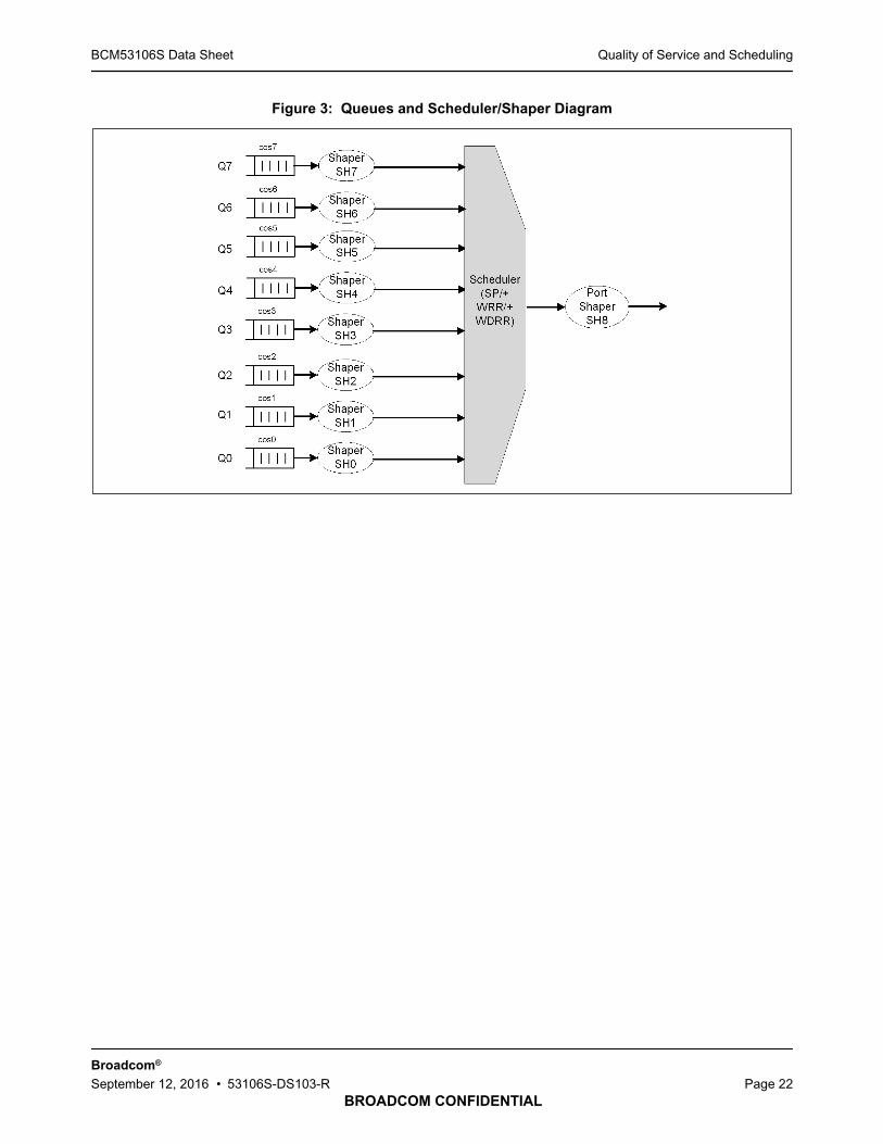
Egress Transmit Queues
Each Ethernet egress port has eight transmit queues (CoS0–CoS7). Each CoS queue has its own dedicatedcounter to measure the buffer occupancy of the queue for congestion management purposes. Every Ethernet(ingress) port has its own set of counters to measure the buffer occupancy and the arrival rate related to thetraffic received from the port.
The IMP (egress) port and port 5 also serve eight transmit queues. When the IMP port (or port 5) is set in non-aggregation mode (i.e., IMP port is configured as a management port to CPU), the CoS (output queue) isdecided based on the reasons for forwarding the packets to the CPU. When the IMP port (port 5) is set inaggregation mode (i.e., IMP port is configured as a regular data uplink port), the CoS is decided from the TCbased the normal packet classification flow.
For the rest of Ethernet egress ports, all incoming frames are assigned to an egress transmit queue dependingon their assigned TC. Each egress transmit queue is a list that specifies an order for packet transmission. Thecorresponding egress port transmits packets from each of the queues according to a programmable algorithm,with the higher TC queues being given greater access than the lower TC queues. Queue 0 is the lowest-TCqueue.
The queues and scheduler/shaper for each port are shown in the Figure 3 on page 22.
Note: In addition to determining the CPU queue in nonaggregation mode, the reason code may alsohelp software process the packet in all modes. In aggregation mode, however, the CoS is determinedby the same TC2COS hardware mapping function that is used for network ports.
Quality of Service and SchedulingBCM53106S Data Sheet
BROADCOM CONFIDENTIAL
Broadcom®
September 12, 2016 • 53106S-DS103-R Page 22
Figure 3: Queues and Scheduler/Shaper Diagram

Quality of Service and SchedulingBCM53106S Data Sheet
BROADCOM CONFIDENTIAL
Broadcom®
September 12, 2016 • 53106S-DS103-R Page 23
Scheduler
The scheduling element can be configured to be one of the following operating modes:
1. Strict Priority.
2. Weighted Round Robin (WRR): packet-based scheduling.
3. Weighted Deficit Round Robin (WDRR): byte-based scheduling.
4. Or a mix of SP, WRR, and WDRR.
Table 1 lists various configuration options of the scheduler.
The operating mode of a scheduling queue/port can be configured independent of the operating mode of anyother scheduling queue/port in the device. One of the two round robin scheduling algorithms (WRR or WDRR)is selected through a per-port configuration register.
Within the SP group, the precedence takes the ascending order of the CoS number. The higher the CoS number,the higher the precedence for scheduling.
Within the WDRR group, the queues are selected based on the following round-robin rules:
• The share can be weighted by assigning each queue its corresponding Weight in granularity of 1/256. IfCoS2 is assigned a weight of x/256, CoS1 is assigned a weight of y/256, and CoS0 is assigned a weight ofz/256, the ratio of transmitted packet bytes between Cos2:CoS1:CoS0 should be x:y:z in each SchedulingRound, if there is always a packet waiting during the round.
• A Scheduling Round is defined as a period within which each queue gets its fair share of packettransmission resource in granularity of number of packets or number of sets of 256 bytes transmitted.
• At the beginning of each scheduling round:
– Every queue’s share is added to its respective accumulated credit, and
– Empty queues are noted and are not considered for scheduling in the scheduling round.
• During each scheduling round, queues with positive credits in respective queue shaper are serviced inorder of CoS (CoS7, CoS6, CoS5,….CoS0):
Table 1: Scheduler Configuration Selections
CoS7 CoS6 CoS5 CoS4 CoS3 CoS2 CoS1 CoS0
Option 1 SP SP SP SP SP SP SP SP
Option 2 SP WDRR/WRR
WDRR/WRR
WDRR/WRR
WDRR/WRR
WDRR/WRR
WDRR/WRR
WDRR/WRR
Option 3 SP SP WDRR/WRR
WDRR/WRR
WDRR/WRR
WDRR/WRR
WDRR/WRR
WDRR/WRR
Option 4 SP SP SP WDRR/WRR
WDRR/WRR
WDRR/WRR
WDRR/WRR
WDRR/WRR
Option 5 SP SP SP SP WDRR/WRR
WDRR/WRR
WDRR/WRR
WDRR/WRR
Option 6 WDRR/WRR
WDRR/WRR
WDRR/WRR
WDRR/WRR
WDRR/WRR
WDRR/WRR
WDRR/WRR
WDRR/WRR

Quality of Service and SchedulingBCM53106S Data Sheet
BROADCOM CONFIDENTIAL
Broadcom®
September 12, 2016 • 53106S-DS103-R Page 24
– Empty queues as well as queues that do not have positive credits in the respective queue shaper areskipped.
– When a queue is serviced, the number of packets transmitted from the queue depends on one of thetwo modes of operations configured by software:
Burst Mode: one or more packets are transmitted from the queue when its fair share of packet transmissionresources is used up (credit becomes negative), or the queue becomes empty before the current schedulinground for the queue ends. End of current scheduling round for a queue means the queue will not be servicedagain in the current scheduling round.
Non-Burst Mode: one packet is transmitted from each queue in the CoS order (CoS7...0), until the fair shareof packet transmission resources of a queue is used up (credit becomes negative), or the queue becomesempty before the current scheduling round for the queue ends. End of current scheduling round for a queuemeans the queue will not be serviced again in the current scheduling round.
– Also, the negative accumulated credit of a non-empty queue from the current round is carried forwardfrom the current round to the beginning of the next round.
– If a queue becomes empty before its fair share is used up, the current scheduling round for the queueends will mean that the queue will not be serviced again in the current scheduling round. Also, its left-over credit is not carried over to the next scheduling round, which means the deficit counter of an emptyqueue is set to zero (to avoid carrying over accumulated credit history of empty queues). The action ofsetting the accumulated credit to zero is independent of whether the queue became negative afterserving the last packet in the queue, or it was still positive after it served the last packet in the queue.
• The scheduler algorithm goes back to Step “At the beginning of each scheduling round” to start the nextround.
The weights of a WRR/WDRR scheduler can be configured independent of weights of any other WRR/WDRRscheduler in the device.
The scheduler works by first servicing the SP queues. Queues have an intrinsic priority from high to low. Thatis, CoS7 has higher priority than CoS6. The second scheduling option utilizes WRR/WDRR. The WRR/WDRRscheduling discipline interleaves packets from queues based on a configured weight for the queues. That is,when a queue is selected for service the depth of the queue is sampled. Packets are transmitted from the queuein the scheduling round until either the queue becomes empty or the credit counter runs out of credits. Oncethese numbers of packets are serviced, then the next queue is serviced. Queues are serviced in a round-robinfashion (WRR/WDRR) until this process is completed. Queues that do not have packets to send in a round(either empty or do not have positive credits in respective queue shapers), are skipped and not serviced. Aqueue is serviced only once in a round. If a packet arrives in a queue just after the scheduler decided to skip aqueue (because it was empty, became empty) in the current round, the packet will not be serviced in the currentround by the scheduler.
For example, assume the queue weights for CoS3–CoS0 are 4, 3, 2, 1 (or 1024, 768, 512, and 256 bytes)respectively, and the scheduler is configured in burst mode of operation. Note that small weights have beenused in this example for simplification. In real applications, the minimum (WDRR weight * 256) should be >=MTU for correct behavior of the WDRR scheduler. Because of programming error, if the weight of any DRRqueue is configured such that (WDRR weight * 256) < MTU, the behavior of the DRR scheduler is notpredictable.

Quality of Service and SchedulingBCM53106S Data Sheet
BROADCOM CONFIDENTIAL
Broadcom®
September 12, 2016 • 53106S-DS103-R Page 25
Assume an example of a scheduling round is similar to Figure 3 on page 22 where the frames are queued onlyin CoS3, CoS1, and CoS0. CoS2 is empty through the entire round in this example. The egress packet streamcreated by the WDRR scheduler is depicted where the number in a rectangle indicates the length of the packetin bytes. In the example, the WDRR scheduler creates an egress packet stream by interleaving packets fromCoS3, CoS1, and CoS0 (the non-empty queues with accumulated weight > 0) in a fashion that depends on theWDRR weights assigned to the respective CoS.
In the example, assume a scheduling round started with zero accumulated credit for each of the four CoSqueues. The WDRR scheme will add credits to the four queues at the beginning of the round. Hence, there willbe 1024 bytes accumulated credits for CoS3, 0 for CoS2, 512 for CoS1, and 256 for CoS0. CoS2 accumulatedcredits at the beginning of the round is 0 since it was either empty, or its shaper was blocked, or the shaper wasenabled but did not have positive credits. In the current round the WDRR scheduler will service the queues inthe following order:
1. The scheduler will service CoS3 first because it is the highest order CoS queue that has positive credits inthe current round. In the example CoS3 has 494 bytes in four packets whereas its accumulated credits are1024 bytes. Hence, it became empty when it still had 530 positive accumulated credits. However, since thequeue became empty before it could use up all its credits, the WDRR scheme will carry forward 0accumulated credits for CoS3 to the next round. The scheduler will not service CoS3 any more in the currentround even if a new packet is stored in the queue while it is servicing any remaining queues in the currentround.
2. It will skip CoS2 next because it has 0 accumulated credits. The scheduler will carry forward 0 accumulatedcredits to the next round for CoS2. The scheduler will not service CoS2 any more in the current round evenif a new packet is stored in the queue while it is servicing the remaining queues in the current round.
3. It will service CoS1 next because it has the next highest order CoS queue. CoS1 has 780 bytes in fourpackets which is a more than 512 bytes of accumulated credits. Hence, the WDRR scheduler will stopservicing the queue and carry forward -278 accumulated credits for CoS1 to the next round after the firstthree packets from the queue are transmitted. The scheduler will not service CoS1 any more in the currentround even if a new packet is stored in the queue while it is servicing the remaining queues in the currentround.
4. Finally, it will serve CoS0 and then end the current round. CoS0 has 204 bytes in two packets which is a littleless than 256 bytes of accumulated credits for CoS1. Since the queue will become empty before its positivecredits are used up, the WDRR scheduler will carry forward 0 credits for CoS0 to the next round. Thescheduler will not service CoS0 any more in the current round even if a packet arrives before the next roundstarts.
Scheduling
There are three shapers, SH2, SH1, and SH0, and they can be separately configured to be either a credit-basedAVB shaper that is compliant with the IEEE 802.1qav standard, or a standard Leaky Bucket rate limiter.

Quality of Service and SchedulingBCM53106S Data Sheet
BROADCOM CONFIDENTIAL
Broadcom®
September 12, 2016 • 53106S-DS103-R Page 26
Leaky Bucket Shaper
Initially, the bucket is filled with tokens with a burst size (B). In every refresh interval, certain amounts of tokensare removed from the bucket, which effectively determines the shaping rate. The scheduler services a packetbased on the state information of the shaper. If the bucket count is less than or equal to the burst size, the packetis in-profile. Otherwise, the packet is out-of-profile. After servicing a packet, tokens are added into the bucket byan amount of tokens equivalent to the size of the packet. In the BroadSync™ HD (AVB) shaping mode, thefollowing additional token updates are required to reduce the burstiness of the EAV traffic. After the bucketcounter is updated, if the queue is empty and the bucket counter is less than the burst size (B), reset the bucketcounter to be equal to burst size (B). See Figure 4.
Figure 4: Leaky Bucket Shaper
The leaky bucket shaper has the following parameters:
• Refresh Interval (I): Defines the how often the tokens are removed from the buckets.
• Shaping Rate (R): The rate at which the shaper limits service.
• Burst Size (B): The maximum number of tokens that can be added into the bucket.
• AVB Shaping Mode: Used to select AVB vs. Normal shaping mode.
In every refresh interval, T tokens are removed from the bucket. T is the number of tokens. Associated with atoken is a token size (S). The shaper operates in byte-based mode, and the token size (S) is the number of bytesper token.
The relation between Shaping Rate (R), Refresh Interval (I) and Token Size (S) can be represented by formula:
R = T x (S/I)

Port-Based VLANBCM53106S Data Sheet
BROADCOM CONFIDENTIAL
Broadcom®
September 12, 2016 • 53106S-DS103-R Page 27
It is recommended that software configure the two shapers in the following way when applicable:
• SH2 should be configured as:
– An AVB shaper for an AVB port with Class A traffic.
– A non-AVB shaper in all other applications.
• SH1 should be configured as:
– An AVB shaper for an AVB port with Class B traffic.
– A non-AVB shaper in all other applications.
• SH0 should be configured as a non-AVB shaper in all applications.
The Leaky Bucket threshold of a shaper can be configured in the range of 64 byte–16 MB, with a resolution of64 byte. When the shaper operates as an AVB shaper, the number of tokens in the shaper is saturated byhardware (made equal to the configured threshold) when there is no packet at the shaper input. For example, ifSH2 is configured as an AVB shaper and Q5 is empty, then hardware forces the accumulated credits in SH2 tobe the same as the threshold. Each shaper output rate can be configured in the range of 64 Kbps–1 Gbps, witha resolution of 64 Kbps.
Port-Based VLAN
The port-based virtual LAN (VLAN) feature partitions the switching ports into virtual private domains designatedon a per-port basis. Data switching outside of the port’s private domain is not allowed. The BCM53106S provideflexible VLAN configuration for each ingress (receiving) port.
The port-based VLAN feature works as a filter, filtering out traffic destined to nonprivate domain ports. For eachreceived packet, the ARL resolves the DA and obtains a forwarding vector (list of ports to which the frame willbe forwarded). The ARL then applies the VLAN filter to the forwarding vector, effectively masking out thenonprivate domain ports. The frame is forwarded only to those ports that meet the ARL table criteria, as well asthe port-based VLAN criteria.
IEEE 802.1Q VLAN
The BCM53106S support IEEE 802.1Q VLAN and up to approximately 4096 VLAN table entries that reside inthe internal embedded memory. Once the VLAN table is programmed and maintained by the microcontroller,the BCM53106S autonomously handle all operations of the protocol. These actions include the stripping oradding of the IEEE 802.1Q tag, depending on the requirements of the individual transmitting port. It alsoperforms all the necessary VLAN lookups in addition to MAC L2 lookups.
Note: The refresh interval is fixed at 7.8125 µs.

Double-TaggingBCM53106S Data Sheet
BROADCOM CONFIDENTIAL
Broadcom®
September 12, 2016 • 53106S-DS103-R Page 28
IEEE 802.1Q VLAN Table Organization
Each VLAN table entry, also referred to as a VLAN ID, an Untag map, and a forward map.
• The untag map controls whether the egress packet is tagged or untagged.
• The forward map defines the membership within a VLAN domain.
• The FWD_MODE indicates whether the packet forwarding should be based on VLAN membership or onARL flow.
The untag map and forward map include bit-wise representation of all the ports.
Figure 5: VLAN Table Organization
Double-Tagging
The BCM53106S provide the double tagging feature, which is useful for ISP applications. When the ISPaggregates incoming traffic from each individual customer, the extra tag (double tag) can provide an additionallayer of tagging to the existing IEEE 802.1Q VLAN. The ISP tag (extra tag) is a way of separating individualcustomers from other customers. Using the IEEE 802.1Q VLAN tag, the individual customer’s traffic can beidentified on a per-port basis.
When the double-tagging feature is enabled (register Page 34h, Address 05h, bit[3:2]) and the Enable IEEE802.1Q (register Page 34h, Address 00h, bit 7), users can expect two VLAN tags in a frame: the tag close toMAC_SA is the ISP tag, and the one following is the customer tag as shown in Figure 6 on page 29.
Note: If the MII port is configured as a management port, then the tag is not stripped even if the untagbit is set.
Entry 0 MSTP_Index UNTAG_MAP[8:0] FORWARD_MAP[8:0]
Entry 1
Entry 2
Entry 4095
FWD_MODE

Double-TaggingBCM53106S Data Sheet
BROADCOM CONFIDENTIAL
Broadcom®
September 12, 2016 • 53106S-DS103-R Page 29
Figure 6: ISP Tag Diagram
The switch uses the ISP tag for ARL and VLAN table accesses and the customer tag as an IEEE 802.1Q tag.There is a per-chip programmable register Double Tagging TPID register for ISP tag (default = 9100'h). All ISPtags will be qualified by this Tag Protocol ID (TPID) value.
When the double-tagging feature is enabled, all switch ports are separated into two groups: ISP ports andcustomer ports. The BCM53106S performs the normalization process for all ingress frames for both IntelligentDouble Tag (IDT) and Double Tag (DT) modes, whether from the ISP port or customer port. The normalizationprocess is to insert an ISP tag, customer tag, or ISP + customer tag (depending on whether the ingress frameis without tags or with one tag) to allow all ingress frames with double tags. But if the ingress frames are withdouble tags (ISP + customer tag), and the ISP tag TPID matches the TPID specified in the Double Tagging TPIDregister, it does not perform the normalization process. The ISP ports are defined in the ISP Port SelectionPortmap register. When the port(s) corresponding bit(s) are set, that port(s) should be connected to the ISP, andotherwise connected to customers. Each switch device can have multiple ports assigned as ISP ports, and eachISP is uniquely identified using different VLAN forward maps or the port-based VLAN feature.
ISP Port
It is possible for the ISP port to receive three different types of frames: untagged, ISP-tagged, andISP+Customer-tagged frames.
When the double-tagging feature is enabled and the received frame is untagged (or the TPID does not matchwith ISP TPID specified in Double Tagging TPID register, the default ISP tag and customer tag are added, andVLAN ID of ISP tag receives it from the port default VID. The frames are forwarded according to the VLAN table.However, if the Port-Based VLAN Control register is enabled, the egress ports specified in the port-VLAN controlregister override the VLAN table settings. If the received frame is ISP tagged (TPID matches with the ISP tagVLAN ID specified in the double-tagging TPID register), the default customer tag (8100 + default PVID) is added,the ISP VID is used to access the ARL table, and the ISP tag can be stripped on the way out according to theuntagged bit setting in the VLAN table. In addition, ISP port frame can forward to the destination port directlybased on forward port map of VLAN table by setting FWD_MODE bit to 1 of VLAN Table Entry register.
The VLAN ID is generated from the ISP tag, and TC is generated from the ingress frame outer tag.
Customer Port
It is also possible for the Customer port to receive two different types of frames: untagged and Customer-taggedframes.
When the double-tagging feature is enabled, all the ingress frames preform the normalization process to insertan ISP tag or ISP + Customer tag (depending whether the ingress frame is without tags or with one tag) to allowall ingress frames with double tags. The VLAN ID of ISP tag receives it from the port default VID.
MAC_DA MAC_SA Customer_ tag Ty/Len Payload
TPID VID
ISP_TAG

Double-TaggingBCM53106S Data Sheet
BROADCOM CONFIDENTIAL
Broadcom®
September 12, 2016 • 53106S-DS103-R Page 30
The VLAN ID is generated from the ISP tag, and the TC is generated from the ingress frame outer tag.
There are two possible traffic scenarios:
• One scenario is from a customer port to an ISP port.
• The second scenario is from an ISP port to a customer port.
Uplink Traffic (from Customer Port to ISP)
Data traffic is traffic received from the customer port without tags or a customer tag, and the frame is destinedfor an ISP port. The customer ingress port performs a normalization process to allow ingress frames with doubletags (ISP + Customer tag), and the ISP tag VID is based on the port default VID tag.
However, if the ingress frame is with an IEEE 802.1p tag, the VID of IEEE 802.1p tag is changed by the VID ofport default VID tag after the customer port normalization process. The TC does not change.
Control traffic frames can be forwarded to the CPU first and then the CPU forwards to the ISP port if the switchmanagement mode is enabled and if the RESV_MCAST_FLOOD bit=0 in the Global VLAN Control 4 register.In this case, the control frame adds an ISP tag by ingress port and forward to the CPU. The CPU can thenforward it to the ISP port with or without the ISP tag by using the egress-direct feature.
Downlink Traffic (from ISP to Customer Port)
Data traffic frame received from ISP port may or may not have ISP tag attached. When the received frame doesnot have an ISP tag and customer tag, the ISP ingress port does a normalization process to insert double tags(ISP + Customer tag), and the ISP tag VID is based on the port default VID tag. All ARL and VID table accessshould be based on the new tag. The traffic is then forwarded to the customer port through proper VLANconfiguration. Usually, the software configures so the customer Egress port continuously removes the ISP tag.However, it is based on how the untagged map is configured.
Moreover, if the ingress frame is with an 802.1p tag, the VID of 802.1p tag is changed by the VID of port defaultVID tag after the ISP port normalization process. The TC will not change.
The Control traffic is forwarded to the CPU when the switch management mode is enabled and if theRESV_MCAST_FLOOD bit=0 in the Global VLAN Control 4 register. The BCM53106S can also support multipleISP port configurations by enabled the FWD_MODE bit of VLAN Table Entry register.
There are also two ways to separate traffic that belongs to two different ISP customers:
1. Each group (ISP, and customer) is assigned to the same VLAN group, so that traffic does not leak to otherISP.
Note: It is illegal to strip out the ISP tag on the ISP egress port by using the untagged bit setting inthe VLAN table.
Note: Only the VLAN tagged or untagged packets are expected for the ingress of the customer ports.The customer does not add the ISP tags.

Jumbo Frame SupportBCM53106S Data Sheet
BROADCOM CONFIDENTIAL
Broadcom®
September 12, 2016 • 53106S-DS103-R Page 31
2. Use the Port-based VLAN to separate traffic that belongs to a different ISP.
Jumbo Frame Support
The BCM53106S can receive and transmit frames of extended length on ports linked at gigabit speed. Referredto as jumbo frames, these packets are longer than the standard maximum size, but shorter than 9720 bytes.Jumbo packets can be received or forwarded only to 100BASE-T linked ports that are jumbo-frame enabled. Upto 38 buffer memory pages are required for storing the longest allowed jumbo frame. While there is no physicallimitation to the number of ports that can be jumbo enabled, it is recommended that no more than two be enabledsimultaneously to ensure system performance. There is no performance penalty for enabling additional jumboports beyond the potential strain on memory resources that can occur due to accumulated jumbo packets atmultiple ports.
Port Trunking/Aggregation
The BCM53106S supports MAC-based trunking. The trunking feature allows up to four ports to be groupedtogether as a single-link connection between two switch devices. This increases the effective bandwidth througha link and provides redundancy. The BCM53106S allow up to two trunk groups. Trunks are composed ofpredetermined ports and can be enabled using Trunking Group 0 register. Ports within a trunk group must be ofthe same linked speed. By performing a dynamic hashing algorithm on the MAC address, each packet destinedfor the trunk is forwarded to one of the valid ports within the trunk group. This method has several keyadvantages. By dynamically performing this function, the traffic patterns can be more balanced across the portswithin a trunk. In addition, the MAC-based algorithm provides dynamic failover. If a port within a trunking groupfails, the other port within the trunk automatically assumes all traffic designated for the trunk. It allows for aseamless, automatic redundancy scheme. This hashing function can be performed on either the DA, SA, or DA/SA.
Figure 7: Trunking
Port X
Port Y
Port Z
Port 0
Port 1
Port 2
One Pipe
Switch 1 Switch 2
Frame XFrame YFrame Z

WAN PortBCM53106S Data Sheet
BROADCOM CONFIDENTIAL
Broadcom®
September 12, 2016 • 53106S-DS103-R Page 32
WAN Port
The BCM53106S offers a programmable WAN port feature: It has a WAN Port Select register (page 00h,address 26h). Select a port as a WAN port, then all that port’s traffic is forwarded to the CPU port only. ThenonWAN port traffic from all other local ports does not flood to the WAN port.
Figure 8 shows the WAN and LAN domain separation when the WAN port is selected.
Figure 8: WAN and LAN Domain Separation
Rate Control
Ingress Rate Control
Forwarding broadcast traffic consumes switch resources, which can negatively impact the forwarding of othertraffic. The rate-based broadcast storm suppression mechanism is used to protect regular traffic from anoverabundance of broadcast or multicast traffic. This feature monitors the rate of ingressed traffic ofprogrammable packet types. If the rates of these packet types exceed the programmable maximum rate, thepackets are dropped.

Rate ControlBCM53106S Data Sheet
BROADCOM CONFIDENTIAL
Broadcom®
September 12, 2016 • 53106S-DS103-R Page 33
The broadcast storm suppression mechanism works on a credit-based rate system that figuratively uses abucket to track the bandwidth of each port (see Figure 9). Credit is continually added to the bucket at aprogrammable bucket bit rate. Credit is decremented from the bucket whenever one of the programmablepacket types is ingressed at the port. If no packets are ingressed for a considerable length of time, the bucketcredit continues to increase up to a programmable-maximum bucket size. If a heavy burst of traffic is suddenlyingressed at the port, the bucket credit becomes drained. When the bucket is emptied, incoming traffic isconstrained to the bucket bit rate (the rate at which credit is added to the bucket). At this point, excess packetsare either dropped or deterred using flow control, depending upon the Suppression Drop mode.
Figure 9: Bucket Flow
Two-Bucket System
For added flexibility, the BCM53106S employs two buckets to track the rate of ingressed packets. Each of thetwo buckets (Bucket 0 and Bucket 1) can be programmed to monitor different packet types. For example, Bucket0 could monitor broadcast packets, while Bucket 1 monitors multicast packets. Multiple packet types can bemonitored by each bucket, and a packet type can be monitored by both buckets.
The rates of each bucket can be individually programmed. For example, the broadcast packets of Bucket 0 couldhave a maximum rate of 3 Mbps, whereas the multicast packets of Bucket 1 could be allowed up to 80 Mbps.The size of each bucket can be programmed. This determines the maximum credit than can accumulate in eachbucket. The Rate Count and Bucket Size can be individually programmed for each port, providing another levelof flexibility. Suppression control can be enabled or disabled on a per-port basis. This system allows the user tocontrol dual packet-type rates on a per-port basis.
Accumulated Credit
BUCKET 1 BUCKET 2
Accumulated Credit
Bucket 2 Bit Rate
Ingress Packet Rate
assigned to Bucket 2
If there is no accumulated credit available, the switch does not accept input packets .
Ingress Packet Rate assigned to Bucket 1
Bucket 1 Bit Rate

Protected PortsBCM53106S Data Sheet
BROADCOM CONFIDENTIAL
Broadcom®
September 12, 2016 • 53106S-DS103-R Page 34
Egress Rate Control
The BCM53106S monitors the rate of egress traffic per port. Unlike the Ingress traffic rate control, the EgressRate Control provides only the per-port rate control regardless of traffic types. This feature uses only one bucketto track the rate of egressed packets. The Egress Rate Control feature supports only absolute bit rate mode (BitRate Mode = 0), and the bucket bit rate calculation is shown in Table 2.
Bucket Bit Rate
The relative ingress rates of each bucket can be programmed on a per-port basis. Each port has aprogrammable Rate Count value for Bucket 0 and Bucket 1. Additionally, the bit rate mode is programmed on achip basis. If this bit is 1, the packet rate is automatically scaled according to the port link speed. Ports operatingat 1000 Mbps would be allotted a 100 times higher ingress rate than ports linked at 10 Mbps. Together, the RateCount value and the bit rate mode determine the bucket bit rate, which is a reflection of how quickly data canbe ingressed (Kbps) at the given port for a given bucket. The Rate Count values are specified in Table 2. Valuesoutside these ranges are not valid entries.
Protected Ports
The Protected Ports feature allows certain ports to be designated as protected. All other ports are unprotected.Traffic between protected port group members is blocked. However, protected ports are able to send traffic tounprotected ports. Unprotected ports can send traffic to any port. Several applications that can benefit fromprotected ports:
• Aggregator: For example, all the available ports are designated as protected ports except a singleaggregator port. No traffic incoming to the protected ports is sent within the protected ports group. Anyflooded traffic is forwarded only to the aggregator port.
• To prevent nonsecured ports from monitoring important information on a server port, the server port andnonsecured ports are designated as protected. The nonsecured ports will not be able to receive traffic fromthe server port.
Table 2: Bucket Bit Rate
Rate Count (RC)Bit RateMode Link Speed
Bucket Bit RateEquation
Approximate ComputedBucket Bit RateValues (as a function of RC)
1–28 0 Any = (RC × 8 × 1M)/125 64 KB, 128 KB, 192 KB,..., 1.792 MB
29–127 0 Any = (RC – 27) × 1M 2 MB, 3 MB, 4 MB,..., 100 MB
128–240 0 Any = (RC – 115) × 1M × 8 104 MB, 112 MB, 120 MB,..., 1000 MB
1–125 1 10 Mbps = (RC × 8 × 1M)/100 0.08 MB, 0.16 MB, 0.24 MB,... 10 MB
1–125 1 100 Mbps = (RC × 8 × 1M)/10 0.8 MB, 1.6 MB, 2.4 MB,..., 100 MB
1–125 1 1000 Mbps = RC × 8 × 1M 8 MB, 16 MB, 24 MB,... 1000 MB
Note: 1M represents 1 × 10⁶.

Port MirroringBCM53106S Data Sheet
BROADCOM CONFIDENTIAL
Broadcom®
September 12, 2016 • 53106S-DS103-R Page 35
Port Mirroring
The BCM53106S support Port Mirroring, allowing ingress and/or egress traffic to be monitored by a single portdesignated as the mirror capture port. The BCM53106S can be configured to mirror the ingress traffic and/oregress traffic of any other port (s). Mirroring multiple ports is possible, but can create congestion at the mirrorcapture port. Several filters are used to decrease congestion.
Enabling Port Mirroring
Port Mirroring is enabled by setting the Mirror Enable bit.
Figure 10: Mirror Filter Flow
Capture Port
The capture port is capable of monitoring other specified ports. Frames transmitted and received at the otherports are forwarded to the Capture port according to the mirror filtering rules discussed below.
Mirror Filtering Rules
Mirror filtering rules consist of a set of three filter operations (Port Mask, Packet Address, and Packet Divider)that are applied to traffic ingressed and/or egressed at a switch port.
Port Mask Filter
The IN_MIRROR_MASK bits define the receive ports that are monitored. The OUT_MIRROR_MASK bits definethe transmit ports that are monitored.
Any number of ingress/egress ports can be programmed to be mirrored, but bandwidth restrictions on the one-mirror capture port should be taken into account to avoid congestion or packet loss.
All
Packets
Port Mask Filter
Ingress Mirror Mask
Port Address Filter
Ingress Mirror Filter
Port Divider Filter
Ingress Mirror Divider
Egress Mirror Mask Egress Mirror Filter Egress Mirror Divider
Capture Port
Destination Port(s)

IGMP SnoopingBCM53106S Data Sheet
BROADCOM CONFIDENTIAL
Broadcom®
September 12, 2016 • 53106S-DS103-R Page 36
Packet Address Filter
The type of filtering that is applied to frames received on the mirrored ports is configurable. TheIN_MIRROR_FILTER bits select among the following:
• Mirror all received frames
• Mirror received frames with DA = x
• Mirror received frames with SA = x
where x is the 48-bit MAC address. Likewise, The type of filtering that is applied to frames transmitted on theegressed mirrored ports.
Packet Divider Filter
The IN_DIV_EN bit allows further statistical sampling. When IN_DIV_EN = 1, the receive frames passing theinitial filter are divided by the value IN_MIRROR_DIV, which is a 10-bit value. Only one out of every n frames isforwarded to the mirror capture port, where n = IN_MIRROR_DIV +1. This allows the following additionalcapabilities:
• Mirror every nth received frame
• Mirror every nth received frame with DA = x
• Mirror every nth received frame with SA = x
IGMP Snooping
The BCM53106S supports IP layer IGMP Snooping which includes IGMP unknown, query, report and leavemessage.
A frame with a value of 2 in the IP header protocol field and IGMP frames are forwarded to the CPU port. Themanagement CPU can then determine, from the IGMP control packets which port should participate in themultigroup session. The management CPU proactively programs the multicast address in the ARL table or themultiport address entries. If the IGMP_UKN_FWD_EN, IGMP_QRY_FWD_EN, IGMP_RPTLVE_FWD_EN isenabled, IGMP frames will be trapped to the CPU port only.
MLD Snooping
The BCM53106S supports IP layer MLD Snooping includes MLD query, report and done message. For the eachof query and report/done message types, there are four options available: discard, forward normally, forward toCPU, or forward normally and copy to CPU. The CPU is then expected to interpret these messages andconfigure the address table accordingly.
Note: When multiple ingress ports have been enabled in the IN_MIRROR_MASK, the cumulative totalpacket count received from all ingress ports is divided by the value of IN_MIRROR_DIV to deliver thenth receive frame to the mirror capture port. Egressed frames are governed by theOUT_MIRROR_MASK bit and the OUT_MIRROR_DIV bit.
IEEE 802.1X Port-Based SecurityBCM53106S Data Sheet
BROADCOM CONFIDENTIAL
Broadcom®
September 12, 2016 • 53106S-DS103-R Page 37
IEEE 802.1X Port-Based Security
IEEE 802.1X is a port-based authentication protocol. By receiving and extracting special frames, the CPU cancontrol whether the ingress and egress ports should forward packets or not. If a user port wants service fromanother port (authenticator), it must get approved by the authenticator. EAPOL is the protocol used by theauthentication process. The BCM53106S detect EAPOL frames by checking the destination address of theframe. The Destination addresses should be either a multicast address as defined in IEEE 802.1X (01-80-C2-00-00-03) or a user-predefined MAC (unicast or multicast) address. Once EAPOL frames are detected, theframes are forwarded to the CPU so it can send the frames to the authenticator server. Eventually, the CPUdetermines whether the requestor is qualified or not based on its MAC_Source addresses, and frames are eitheraccepted or dropped. The per-port EAP can be programmed in the register.
BCM53106S provides three modes for implementing the IEEE 802.1X feature. Each mode can be selected bysetting the appropriate bits in the register.
The Basic Mode (when EAP Mode = 00'b) is the standard mode, the EAP_BLK_MODE bit would be set beforeauthentication to block all of the incoming packets, upon authentication, the EAP_BLK_MODE bit would becleared to allow all the incoming packets. In this mode, the Source Address of incoming packets is not checked.
The second mode is Extended Mode (when EAP Mode = 10'b), where an extra filtering mechanism isimplemented after the port is authenticated. If the Source MAC address is unknown, the incoming packets wouldbe dropped and the unknown SA would not be learned. However if the incoming packet is IEEE 802.1X packet,or special frames, the incoming packets will be forwarded. The definition of the Unknown SA in this case is whenthe switch cannot match the incoming Source MAC address to any of the addresses in ARL table, or theincoming Source MAC address matches the address in ARL table, but the port number is mismatched. The thirdmode is Simplified Mode (when EAP Mode = 11'b). In this mode, the unknown Source MAC address packetswould be forwarded to CPU rather than dropped. Otherwise, it is same as the Extended Mode operation.
Note: The BCM53106S checks only the destination addresses to qualify EAPOL frames. Ethernettype fields, packet type fields, or non-IEEE 802.1Q frames are not checked.

DoS Attack PreventionBCM53106S Data Sheet
BROADCOM CONFIDENTIAL
Broadcom®
September 12, 2016 • 53106S-DS103-R Page 38
DoS Attack Prevention
The BCM53106S supports the detection of the following DoS (Denial of Service) attack types based on registersetting, which can be programmed to drop or not to drop each type of DoS packets respectively.
• MIN_TCP_Header_Size is programmable between 0 and 255 bytes, inclusive. The default value is set to20 bytes (TCP header without options).
• MAX_ICMPv4_Size is programmable between 0 and 9.6 KB, inclusive. The default value is set to 512bytes.
• MIN_TCP_Header_Size is programmable between 0 and 9.6 KB, inclusive. The default value is set to 512bytes.
• The default control setting for all types of DoS attacks is not to drop the DoS attack packet.
• It is globally configurable whether to perform the SA learning operation with the received packets of theDoS attack type defined in the registers, regardless of the individual DoS attack types.
• Once a packet is detected as a DOS attack type that must be dropped, the packet is dropped regardless ofARL forwarding decisions, but its forwarding based on mirroring function is not affected.
Table 3: DoS Attacks Detected by BCM53106S
DoS Attack Type Description
IP_LAND IPDA = IPSA in an IPv4/IPv6 datagram
TCP_BLAT DPort = SPort in a TCP header carried in an unfragmented IP datagram or in the firstfragment of a fragmented IP datagram
UDP_BLAT DPort = SPort in a UDP header carried in an unfragmented IP datagram or in the firstfragment of a fragmented IP datagram
TCP_NULLScan Seq_Num = 0 and all TCP_FLAGs = 0 in a TCP header carried in an unfragmented IPdatagram or in the first fragment of a fragmented IP datagram
TCP_XMASScan Seq_Num = 0 , FIN = 1, URG = 1, and PSH = 1 in a TCP header carried in anunfragmented IP datagram or in the first fragment of a fragmented IP datagram
TCP_SYNFINScan SYN = 1 and FIN = 1 in a TCP header carried in an unfragmented IP datagram or in thefirst fragment of a fragmented IP datagram
TCP_SYNError SYN = 1, ACK = 0, and SRC_Port<1024 in a TCP header carried in an unfragmentedIP datagram or in the first fragment of a fragmented IP datagram
TCP_ShortHDR The length of a TCP header carried in an unfragmented IP datagram or the firstfragment of a fragmented IP datagram is less than MIN_TCP_Header_Size
TCP_FragError The Fragment_Offset = 1 in any fragment of a fragmented IP datagram carrying part ofTCP data
ICMPv4_Fragment The ICMPv4 protocol data unit carried in a fragmented IPv4 datagram
ICMPv6_Fragment The ICMPv6 protocol data unit carried in a fragmented IPv6 datagram
ICMPv4_LongPing The ICMPv4 ping (echo request) protocol data unit carried in an unfragmented IPv4datagram with its Total Length indicating a value greater than the MAX_ICMPv4_Size+ size of IPv4 header
ICMPv6_LongPing The ICMPv6 ping (echo request) protocol data unit carried in an unfragmented IPv6datagram with its payload length indicating a value greater than the MAX_ICMPv6_Size

Multiple Spanning Tree ProtocolBCM53106S Data Sheet
BROADCOM CONFIDENTIAL
Broadcom®
September 12, 2016 • 53106S-DS103-R Page 39
Multiple Spanning Tree Protocol
The BCM53106S support up to eight multiple spanning trees. When the EN_RX_BPDU bit = 1, the BCM53106Sforwards BPDU packets to the management port only.
Software Reset
The BCM53106S provides Software Resets. Software Resets can be triggered by setting the register (page 00h,address 79h).
BroadSync HD
BroadSync HD is the enhancement to IEEE 802.3 MAC and IEEE 802.1D bridges to support the kind of low-latency isochronous services and guaranteed QoS that is required for many consumer electronics applications.
BCM53106S provides the BroadSync HD feature. BCM53106S always forwards BPDU, MRP packets to CPUfor BroadSync HD applications, and handle IEEE 802.1 Time Sync Protocol.
The BCM53106S can identify a packet as a Broadsync HD packet if MAC DA matches with the programmed(registered and configured based on MRP protocols) MAC address. A MAC address can be a multicast orunicast address. The PCP of the incoming Broadsync HD packet can be any value that is programmed. Thedefault values are 4 and 5.There are two dedicated queues for BroadSync HD Class 5 and Class 4 traffic peregress port. The BCM53106S enhances shaping and scheduling for BroadSync HD operation.
Time Base and Slot Generation
For BroadSync HD applications, the BCM53106S maintains a time base (32-bit counter) running at a granularityof 1 ns, which can be adjusted by CPU for synchronization with the BroadSync HD time master unit (Switch orHost) through the IEEE 802.1 Time Synchronized (TS) protocol (to be standardized). The TS protocol isimplemented by the CPU which requires the BCM53106S to perform the following operations.
• A received TS protocol packet is timestamped at the ingress port when the first byte (of MACDA) arrives,and is transferred along with the receiving timestamp to the CPU.
• A TS protocol packet initiated by the CPU (to be transmitted at an egress port) is timestamped at theegress port when the first byte (of MACDA) is transmitted, and the transmit timestamp recorded at theegress port is reported back to CPU.
It is required that the time synchronization point peers over an Ethernet link is chosen such that the link delayis perceived as constant, and the protocol exchange occurs at least every 10 ms over every link.
Note: Software Reset sets all the register and the table (ARL, VLAN) contents to the default values.Software Reset will not latch in the strap pin values, but the previous latched strap pin values areretained.

BroadSync HDBCM53106S Data Sheet
BROADCOM CONFIDENTIAL
Broadcom®
September 12, 2016 • 53106S-DS103-R Page 40
The CPU may be required to speed up or slow down the timebase maintained in BCM53106S based on the TSprotocol execution. The BCM53106S provides the time base adjustment mechanism for graceful time changesbased on CPU instructions.
In addition, the BCM53106S maintains counter mechanism to generate time Slot for BroadSync HD trafficscheduling.
• A Slot is defined as 125 s, it is used to pace the BroadSync HD Class 5 traffic which has tight jitterrequirements;
• A MacroSlot is configurable as 1 ms, 2 ms, or 4 ms (binary number of Slots). It is used to pace theBroadSync HD Class4 traffic which has relaxed jitter requirements.
The CPU may be required to make the Slot wider or narrower based on the TS protocol execution. TheBCM53106S provides the Slot adjustment mechanism for graceful Slot width changes based on CPUinstructions.
Transmission Shaping and Scheduling
BroadSync HD Class5 Media Traffic
The CoS5 queue is dedicated for BroadSync HD Class 5 traffic only, and a CoS5 packet is always the highestpriority to be scheduled for transmission, if it is allowed by the Shaper A that operates as follows.
• The Shaper A is an emulation of fixed bandwidth pipe for Class 5 BroadSync HD traffic with tight jitter tohandle interference from non-BroadSync HD or Class 4 BroadSync HD traffic adaptively. Note that thepreamble and IPG transmission are not taken into account for the pipe operation.
• Tunable parameters for the Shaper A are listed as follows.
– MaxAVPacketSize indicates the maximum packet size allowed on an AV-Enabled port. It is a globalsetting using BroadSync HD Max Packet Size register.
– Class5_BW indicates the reserved bandwidth for Class 5 BroadSync HD traffic at granularity of Byte(per Slot, 125 µs). It is a per-port setting.
– Class5_Window indicates the jitter control for Class5 BroadSync HD transmission. It is a per-portsetting.
• At the start of each Slot:
– Reset the credit in the shaping bucket to Class5_BW, if the queue is empty.
– Reset the credit in the shaping bucket to Class5_BW, if the queue is not empty and Class5_Window isset to 0.
– Reset the credit in the shaping bucket to Class5_BW, if the queue is not empty, Class5_Window is setto 1, and the credit remained in the shaping bucket is greater than MaxAVPacketSize.
– Add Class5_BW to the credit in the shaping bucket, if the queue is not empty, Class5_Window is set to1, and the credit remained in the shaping bucket is less than or equal to MaxAVPacketSize.
• The credit in the shaping bucket decrements for every byte transmitted for the Class 5 BroadSync HDtraffic through the port.
– If the credit reaches 0 before the end of the current Slot while transmitting a Class 5 BroadSync HDpacket, the ongoing packet transmission is not interrupted and the credit stays at 0 until being reset atthe start of next Slot.

BroadSync HDBCM53106S Data Sheet
BROADCOM CONFIDENTIAL
Broadcom®
September 12, 2016 • 53106S-DS103-R Page 41
– The credit decrements resumes at the next Slot if the ongoing transmission continues.
• As long as the credits in the shaping bucket is greater than 0, a Class 5 BroadSync HD packet is allowed tobe scheduled for transmission.
BroadSync HD Class4 Media Traffic
The COS4 queue is dedicated for BroadSync HD Class 4 traffic only, and a CoS4 packet always yield to CoS5traffic (if allowed to be scheduled), but takes precedence over the traffic from CoS0~CoS3 queues or follow theweight ratio between CoS4 and CoS0~CoS3 for transmission scheduling, if it is allowed by the Shaper B thatoperates as follows.
• The Shaper B is an emulation of fixed bandwidth pipe for Class 4 BroadSync HD traffic with relaxed jitter tohandle interference from non-BroadSync HD or Class 5 BroadSync HD traffic adaptively. It also statisticallylevels the Class 4 BroadSync HD transmission bursts towards the next hop switch to reduce the bufferingrequirements by using Slot (instead of MacroSlot) as the pacing mechanism. The preamble and IPGtransmission are not accounted for in the pipe operation.
• Tunable parameters for the Shaper B are listed as follows:
– MacroSlot_Period indicates the periodic cycle time to shape the Class 4 traffic. It is a global setting toindicate 1 ms, 2 ms, or 4 ms.
– MaxAVPacketSize indicates the maximum packet size allowed on an AV-Enabled port. It is a globalsetting. (same as for BroadSync HD Class 5 setting)
– Class4_BW indicates the evenly divided bandwidth share per Slot, which is derived from dividing thereserved bandwidth for Class 4 BroadSync HD traffic at granularity of Byte (per MacroSlot) by thenumber of Slots within a MacroSlot. It is a per-port setting.
• At the start of each Slot,
– If the Slot is the first one for the current MacroSlot, reset the credit bucket toClass4_BW+MaxAVPacketSize; (MaxAVPacketSize is used as the deficit base)
– Otherwise, add Class4_BW to the credit in the shaping bucket.
• The shaping credit bucket decrements for every byte transmitted for the Class 4 BroadSync HD traffic.
As long as the credits in the shaping bucket is greater than or equal to MaxAVPacketSize, a Class 4 BroadSyncHD packet is allowed to be scheduled for transmission

CableCheckerBCM53106S Data Sheet
BROADCOM CONFIDENTIAL
Broadcom®
September 12, 2016 • 53106S-DS103-R Page 42
CableChecker
The BCM53106S provide the cable diagnostic capabilities for unmanaged environments. The actual cablediagnostic feature lies in the PHY functional block. The BCM53106S devices let the user monitor the cablediagnostic results through LED display by setting the appropriate bits in the LED refresh registers.
The BCM53106S uses the existing LED display (which is already assigned to various functions) to indicate thecable diagnostic results. Table 4 shows the cable diagnostic result output for each LED function where 1 and 0represent the LED indication pin status; 1 indicates active and 0 indicates inactive.
Note:
• The best way for a user to visualize the cable diagnostic test result through LEDs is to bring outthe LINK status bit to the LED display along with other functions to be displayed per port. In thisway, the user can observe the cable diagnostic result from the flashing (or lit) LED of otherfunctions while LINK LED is off. The switch will turn off the LINK status LED during the cablediagnostic mode.
• The cable diagnostic is expected to be most effective when the user cannot establish the link withthe partner.
Table 4: Cable Diagnostic Output
LED Function in LED Function Register Cable Diagnostic Output
PHYLED4 1 = Cable diagnostic failed0 = Cable diagnostic passed
LNK No output during the cable diagnostic mode
DPX 1 = Passed0 = Failed
ACT 1 = Passed0 = Failed
COL 1 = Passed0 = Failed
LNK/ACT No output during the cable diagnostic mode
DPX/COL 1 = Passed0 = Failed
SPD10M 1 = Failed0 = Passed
SPD100M In LED function0 map1 = Cable diagnostic passed0 = FailedIn LED function1 map1 = Cable diagnostic failed0 = Passed

Egress PCP RemarkingBCM53106S Data Sheet
BROADCOM CONFIDENTIAL
Broadcom®
September 12, 2016 • 53106S-DS103-R Page 43
Egress PCP Remarking
The BCM53106S provides an egress PCP remarking feature of the outer tag at each egress port which includesthe CFI and PCP field modification based on the internal ARL generated TC Rate Violation (RV) status. TheEgress PCP remarking process applies to Ethernet ports only. Each Ethernet port can provide a 16-entrymapping table indexed by {RV, TC} to map to the {New CFI, New PCP} field for the outgoing packet.
SPD1G 1 = Passed0 = Failed
10M/ACT 1 = Failed0 = Passed
100M/ACT In LED function0 map1 = Cable diagnostic passed0 = FailedIn LED function1 map1 = Cable diagnostic failed0 = Passed
10–100M/ACT 1 = Failed0 = Passed
1G/ACT 1 = Passed0 = Failed
PHYLED3 1 = Failed0 = Passed
Note: For the AV-enabled egress port, the egress PCP for the non-BroadSync HD class of traffic mustnever be programmed with values of 100 and 101.
Table 4: Cable Diagnostic Output (Cont.)
LED Function in LED Function Register Cable Diagnostic Output

Address ManagementBCM53106S Data Sheet
BROADCOM CONFIDENTIAL
Broadcom®
September 12, 2016 • 53106S-DS103-R Page 44
Address Management
The BCM53106S Address Resolution Logic contains the following features:
• Four bins per bucket address table configuration.
• Hashing of the MAC/VID address to generate the address table point.
The address management unit of the BCM53106S provides wire speed learning and recognition functions. Theaddress table supports 4K unicast/multicast addresses using on-chip memory.
Address Table Organization
The MAC addresses are stored in embedded SRAM. Each bucket contains four entries or bins. The addresstable has 1K buckets with four entries in each bucket. This allows up to four different MAC addresses with thesame hashed index bits to be simultaneously mapped into the address table. In the ARL DA/SA lookup process,it hashes a 10-bit search index and read out bin0 and bin1 in the first cycle, and read out bin2 and bin3 in thesecond cycle. These four entries are used for ARL routing and learning.
Figure 11: Address Table Organization
The index to the address table is computed using a hash algorithm based on the MAC address and the VLANID (VID) if enabled.
MAC Address [47:0]HASH
FunctionVID [11:0]
Hash Index [9:0]
bin0 bin1
bin3bin2
4K ARL Table
000000
0003FF
V S A TC CON Rsvd PortID MACADDRVID[11:0]
V S A TC CON MCAST MAP MACADDRVID[11:0]
Unicast Address
Multicast Address
Four bins per index

Address ManagementBCM53106S Data Sheet
BROADCOM CONFIDENTIAL
Broadcom®
September 12, 2016 • 53106S-DS103-R Page 45
The hash algorithm uses the CRC-CCITT polynomial. The input to the hash is reduced to a 16-bit CRC hashvalue. Bits [9:0] of the hash are used as an index to the approximately 4K locations of the address table.
The CRC-CCITT polynomial is:
x16 + x12 + x5 + 1
Address Learning
Information is gathered from received unicast packets and learned or stored for the future purpose of forwardingframes addressed to the receiving port. During the receive process, the frame information (such as the SourceAddress [SA] and VID) is saved until completion of the packet. An entry is created in the ARL table memory ifthe following conditions are met:
• The packet has been received without error.
• The packet is of legal length.
• The packet has a unicast SA.
• If using IEEE 802.1Q VLAN, the packet is from an SA that belongs to the indicated VLAN domain.
• The packet does not have a reserved multicast destination address. This condition can be disabled usingregister settings.
• There is free space available in memory to which the hashed index points.
When unicast packets are dynamically learned, the VALID bit is set, the AGE bit is set, and the STATIC bit iscleared in the entry. See Table 6 on page 46 for a description of a unicast ARL entry.
Multicast addresses are not learned into the ARL table, but must be written using one of the “ProgrammingInterfaces” on page 78.
Address Resolution and Frame Forwarding
Received packets are forwarded based on the information learned or written into the ARL table. Addressresolution is the process of locating this information and assigning a forwarding destination to the packet. Thedestination address (DA) and VID of the received packet are used to calculate a hashed index to the ARL table.The hashed index key is used by the address resolution function to locate a matching ARL entry. The frame isassigned a destination based on the forward field (PORTID or IPMC0) of the ARL entry. If the address resolutionfunction fails to return a matching ARL entry, the packet is flooded to all appropriate ports. The following twosections describe the specifics of address resolution and frame forwarding for “Unicast Addresses” on page 46and “Multicast Addresses” on page 47.
Note: In the Enable IEEE 802.1Q and VLAN Learning Mode both the MAC address and the VLAN ID(VID) are used to compute the hashed index. See “IEEE 802.1Q VLAN” on page 27 for more information.
Address ManagementBCM53106S Data Sheet
BROADCOM CONFIDENTIAL
Broadcom®
September 12, 2016 • 53106S-DS103-R Page 46
Unicast Addresses
Frames containing a unicast destination address are assigned a forwarding field corresponding to a single port.The unicast address-resolution algorithm are as follows:
• If the multiport addressing feature is enabled and the DA matches one of the programmed multiportaddresses, then it is forwarded accordingly. See “Power Savings Modes” on page 50.
• The lower 10 bits of the hashed index key are used as a pointer into the address table memory, and theentry is retrieved.
• If the valid indicator is set and the address stored at one of the locations matches the index key of thepacket received, the forwarding field port ID is assigned to the destination port of the packet.
– If the destination port matches the source port, the packet is not forwarded.
• If the address resolution function fails to return a matching valid ARL entry and the unicast DLF forward bitis set, the frame is forwarded according to the port map.
• Otherwise, the packet is flooded to all appropriate ports.
See Table 5 for definitions of the unicast index key and the assigned forwarding field. The forwarding field for aunicast packet is the port ID contained in the matching ARL entry. See Table 6 for a description of a unicast ARLentry.
Multicast ARL table entries are described in Table 7 on page 47.
Table 5: Unicast Forward Field Definitions
EN_1QVLAN Index Key Forwarding Field
1 DA and VID Port ID
0 DA Port ID
Table 6: Address Table Entry for Unicast Address
Field Description
VID VLAN ID associated with the MAC address
VALID 1 = Entry is valid.0 = Entry is empty.
STATIC 1 = Entry is static—Should not be aged out and is written and updated by software.0 = Entry is dynamically learned and aged.
AGE 1 = Entry has been accessed or learned since last aging process.0 = Entry has not been accessed since last aging process.
TC MACDA-based TC (valid only for static entries). See “Quality of Service and Scheduling”on page 18 for more information.
Reserved –
Reserved Only 00 is valid.
PORTID Port identifier. The port associated with the MAC address.
MAC ADDRESS 48-bit MAC address.

Address ManagementBCM53106S Data Sheet
BROADCOM CONFIDENTIAL
Broadcom®
September 12, 2016 • 53106S-DS103-R Page 47
Multicast Addresses
Frames containing a multicast destination address are assigned a forwarding field corresponding to multipleports specified in a port map. If no matching ARL entry is found, the packet is flooded to all appropriate ports.
The multicast address resolution algorithm are as follows:
• If the DA matches one of the globally assigned reserved addresses between 01-80-C2-00-00-00 and 01-80-C2-00-00-2F, the packet is handled as described in Table 8 on page 48.
• If the multiport addressing feature is enabled and the DA matches one of the programmed MultiportAddresses, then it is forwarded accordingly.
• Otherwise, the lower 10 bits of the hashed index key are used as a pointer into the ARL table memory, andthe entry is retrieved.
• If the valid indicator is set, and the address stored at the entry locations matches the index key of thepacket received, the forwarding field port map is assigned to the destination port of the packet.
• If the address resolution function fails to return a matching valid ARL entry and the multicast DLF forwardbit is set, the frame is forwarded according to the port map. There are two types of Multicast addressgroups handled by two separate Lookup Fail Forward registers.
• Otherwise, all other multicast and broadcast packets are flooded to all appropriate ports.
See Table 7 for a description of a multicast ARL entry. See “Accessing the ARL Table Entries” on page 49 formore information.
Unicast ARL table entries are described in Table 6 on page 46.
Table 7: Address Table Entry for Multicast Address
Field Description
VID VLAN ID associated with the MAC address
VALID 1 = Entry is valid.0 = Entry is empty.
STATIC 1 = Entry is static—This entry is not aged out and is written and updated by software.0 = Not defined.
AGE AGE bit is ignored for static ARL table entries.
TC MACDA-based TC (valid only for static entries). See “Quality of Service and Scheduling” onpage 18 for more information.
Reserved –
IPMC0 [8:0] Multicast forwarding mask1 = Forwarding enable.0 = Forwarding disable.
MAC ADDRESS 48-bit MAC address.

Address ManagementBCM53106S Data Sheet
BROADCOM CONFIDENTIAL
Broadcom®
September 12, 2016 • 53106S-DS103-R Page 48
Reserved Multicast Addresses
Table 8 summarizes the actions taken for specific reserved multicast addresses. Packets identified with thesedestination addresses are handled uniquely since they are designed for special functions.
Table 8: Behavior for Reserved Multicast Addresses
MAC Address FunctionIEEE 802.1Specified Action
UnmanagedMode Action Managed Mode Action
01-80-C2-00-00-00 Bridge groupaddress
Drop frame Flood frame Forward frame to IMPonly.
01-80-C2-00-00-01 IEEE 802.3x MACcontrol frame
Drop frame Receive MACdetermines if it is avalid pause frameand then actsaccordingly
Receive MAC determinesif valid pause frame andacts accordingly.
01-80-C2-00-00-02 Reserved Drop frame Drop frame Forward to framemanagement port only.
01-80-C2-00-00-03 IEEE 802.1X port-based networkaccess control
Drop frame Drop frame Forward frame tomanagement port only.
01-80-C2-00-00-04–01-80-C2-00-00-0F
Reserved Drop frame Drop frame Forward frame tomanagement port only.
01-80-C2-00-00-10 All LANs bridgemanagement groupaddress
Forward frame Flood frame Forward frame to all portsincluding managementport.
01-80-C2-00-00-11–01-80-C2-00-00-1F
Reserved Forward frame Flood frame Forward frame to all portsexcluding managementport.
01-80-C2-00-00-20 GMRP address Forward frame Flood frame Forward frame to all portsexcluding managementport, or forward frame tomanagement port only (bysetting bit 4 of page 34,offset 04h register).
01-80-C2-00-00-21 GVRP address Forward frame Flood frame Forward frame to all portsexcluding managementport, or forward frame tomanagement port only (bysetting bit 5 of page 34,offset 04h register).
01-80-C2-00-00-22–01-80-C2-00-00-2F
Reserved Forward frame Flood framea
a. Frames flood to all ports. Certain exclusions apply, such as VLAN restrictions.
Forward frame to all portsexcluding managementport.

Address ManagementBCM53106S Data Sheet
BROADCOM CONFIDENTIAL
Broadcom®
September 12, 2016 • 53106S-DS103-R Page 49
Static Address Entries
The BCM53106S supports static ARL table entries that are created and updated using one of the “ProgrammingInterfaces” on page 78. These entries can contain either unicast or multicast destinations. Static entries do notautomatically learn MAC addresses or port associations and are not aged out by the automatic internal agingprocess.
Accessing the ARL Table Entries
ARL table entries are accessed by one of two mechanisms. The first mechanism uses the ARL read/writecontrol, which allows an address-entry location to be read, modified, or written based on the value of a knownMAC address. The second mechanism searches the ARL table sequentially, returning all valid entries.
Searching the ARL Table
The second method to access the ARL table is through the ARL search control. The entire ARL table is searchedsequentially, revealing each valid ARL entry.
The ARL search and ARL read/write operations execute in parallel with other register accesses. This allows thehost processor to start a read, write, or search process and then read/write other registers, returning periodicallyto see if the operation has completed.
Address Aging
The BCM53106S offers two types of Address Aging processes, Normal Aging process and Fast Aging process.When the address entries are marked as “static” in the ARL table, the Normal Aging process does not apply. Inthis case, the address entries can only be removed by the user, by Fast-Aging, or by RESET.
Normal Aging
The Normal Aging process removes the dynamically learned address entries in the ARL table if the entries arenot accesses (no packets are addressing the MAC address) for the specified period of time in the Aging TimeControl Register (page 02h, address 06h). Users can specify the aging time. Otherwise, the entries will age outby the default time of 300 seconds.
Users can also accelerate the Aging time by enabling the AGE_Accelerate bit (Page 04h, address 00h, bit 2).When this bit is set, the Aging time is reduced to 1/128 of the current Aging time.
Note: The managed mode is set through the register Page 00h, Address 0Bh, bit 0, and amanagement port can be selected through the register Page 02h, Address 00h. The management(IMP) port often has to be forced to link through the IMP Port State Override register Page 00h,Address 0Eh.

Power Savings ModesBCM53106S Data Sheet
BROADCOM CONFIDENTIAL
Broadcom®
September 12, 2016 • 53106S-DS103-R Page 50
Fast Aging
The Fast Aging process removes the address entries in the ARL table selectively specified by the Fast AgingControl Register (page 00h, address 88h). The fast aging function can be enabled per port or per VLAN ID.Users can select and specify the type of entries to be removed in the Fast-Aging Control Register (page 00h,address 88h).
• Multicast entries: multicast cannot be selected at the same time with Port ID selection.
• Spanning Tree ID
• VLAN ID: specified in the Fast-Aging VID Control Register (page 00h, address 8Ah).
• Port ID: specified in the Fast-Aging Port Control Register (page 00h, address 89h).
• Dynamic entries
• Static entries
Users can trigger the Fast-Aging process by setting the Fast-Age-Start bit in the Fast Aging Control Register(page 00h, address 88h). Once the Fast-Aging process is triggered, the process goes through each entry in theARL table and removes the selected type of entry. Entries stored in the lower address are removed first.
Power Savings Modes
The BCM53106S offers different power savings modes for different operating states. All the power savingscheme are implemented without any external CPU requirement.
The various power savings modes are:
• Auto Power Down mode: This is a stand alone PHY feature which is enabled by a register bit setting. ThePHY shuts off the analog portion of the circuitry when cable is not connected or the link partner power isdown.
• Energy Efficient Ethernet (EEE) mode: Energy Efficient Ethernet is IEEE 802.1az, an extension of theIEEE 802.3 standard. IEEE defines support for the PHY to operate in Low Power Idle (LPI) mode. Whenenabled, this mode supports QUIET times during low link utilization, allowing the both sides of link todisable portions of each PHY's operating circuitry and save power.
• Deep Green mode: This mode also requires the CPU to recognize the long period power down time andshut off the PHY power and the PLL to the PHY core. The CPU wakes up the PHY when a signal isdetected at the PHY input.
Auto Power Down Mode
Auto Power Down mode saves PHY power consumption while the link is down. When the user enables the AutoPower Down mode through a PHY register bit setting, the PHY goes into the power savings mode automaticallywhenever it is in link-down state. During the Power Down state, the PHY wakes up every 2.7 or 5.4 seconds,depending on the register settings, and checks for a link signal. If no link signal is detected, then the PHY goesback to Power Down state, or the PHY wakes up and resumes the link process.
Automatic Power Down mode applies to the following conditions:

Power Savings ModesBCM53106S Data Sheet
BROADCOM CONFIDENTIAL
Broadcom®
September 12, 2016 • 53106S-DS103-R Page 51
1. Cable is plugged in, but the link partner is shut down (for example, when a PC is off), so the port is in linkdown state.
2. Cable is unplugged, so the port is in link down state.
Energy Efficient Ethernet Mode
Energy Efficient Ethernet (EEE) power savings mode saves PHY power consumption while the link is up butwhen extended idle periods may exist between packet traffic. In EEE power savings mode PHY powerconsumption is scalable to the actual bandwidth utilization. The PHY can go in to Quiet mode (low-power idlemode) when there is no data to be transmitted. This feature is based on the latest IEEE 802.3az standard. TheEEE supporting capability of the link partner is a must for this feature to work, and the discovery of the capabilityis during auto-negotiation through Link Layer Discovery Protocol (LLDP). This EEE feature is an embeddedPHY feature and no external CPU is required.
In this mode, the MAC determines when to enter low power mode by examining the state of the transmit queuesassociated with each MAC. Four simple adjustments (settings) are used to trigger (optimize) the behavior ofEEE control policy. These adjustments are:
• Global Buffer occupancy threshold
• Two-part sleep delay timer
• Minimum low-power idle duration timer
• Wake transition timer
The two-way communication between the PHY and its link partner is required for the PHY to achieve the powersavings on both sides. The transmit PHY sends a sleep symbol to the link partner, and the link partner enterslow power state. When the transmit PHY sends a wake symbol, the regular packet transfer mode resumes.
For details on how the mode works and how to set up the conditions, refer to the application note, EnergyEfficient Ethernet in the BCM53125 (BCM53125-AN200-R).
Deep Green Mode
The Deep Green Power Savings mode is a step deeper than the Auto Power Down Power Savings mode. TheDeep Green Power Savings mode can be enabled through the internal 8051 microcontroller by setting theEN_8051 strap pin high (default state). The Auto Power Down Power Savings mode is per port, but the DeepGreen Power Savings mode is for all the ports with a common PLL.
When all the ports that are sharing a PLL are linked down, the Auto Power Down mode is enabled (register page10h–14h, address 38h, shadow 01010b), the DLL Auto Power-Down mode is enabled (register page 10h–14h,address 38h, shadow 00101b), and then the PHYs enter the Deep Green Power Savings mode. In this mode,all the PHY circuits are powered down except the energy detection circuit, and the energy detection circuitconstantly monitors the energy on the line. Upon signal energy detection, the microcontroller turns on the PLLalong with PHY power to start the auto-negotiation process. The Deep Green Power Savings mode is mosteffective when the user expects no activities on the line for a long period of time.

InterruptBCM53106S Data Sheet
BROADCOM CONFIDENTIAL
Broadcom®
September 12, 2016 • 53106S-DS103-R Page 52
Interrupt
The BCM53106S has an interrupt feature that can be programmed to generate two types of interrupts. The firsttype of interrupt is generated whenever link status change occurs in any of the ports. The second type ofinterrupt is generated when there is a packet(s) in IMP transmit queue to the CPU using the IMP port. The newtype of interrupt is called IMP Sleep interrupt. The two types of interrupts can be enabled throughInterrupt_Enable_Register (page 03h, address 08h), and both types of interrupts can be enabled together perport. However, the Link Status Change interrupts are normally used on port [4:0], and IMP Sleep interrupts areavailable only on Port 5 and the IMP port.
The purpose of the IMP Sleep interrupt is to wake up the external CPU connected to the IMP (or WAN) portbefore the switch to transmit the queued-up packet to the CPU. This interrupt can be used in any system withthe CPU/switch combination. When there is no traffic to be sent to CPU, the CPU can go into sleep mode toconserve power. However, the CPU must be able to wake up when there is a packet(s) to be received, withoutlosing any packets. For this situation, the BCM53106S can send out an interrupt to wake up the CPU and holdthe packet(s) until the CPU is ready to accept the packets and process. The time to hold the packets to the CPUis programmable by the specific CPU based on its wake-up time requirement. The packet hold time (IMP sleeptime) can be programmed through the register (page 03h, address 10h (for IMP port), address 14h (for Port 5)).
Once the interrupt is generated to wake up the CPU, the switch holds the packet(s) in the transmit queue till theIMP-sleep timer expires. The IMP-sleep timer is also programmable depending on the wake-up time requiredby the CPU.
The CPU has an option to enable each different type of interrupt through the Interrupt-Enable register. Once aninterrupt is generated, the CPU can find out the source of the interrupt by reading the Interrupt Status register.

System Functional BlocksBCM53106S Data Sheet
BROADCOM CONFIDENTIAL
Broadcom®
September 12, 2016 • 53106S-DS103-R Page 53
Section 3: System Functional Blocks
Overview
The BCM53106S includes the following blocks:
• “Media Access Controller”
• “Integrated 10/100 PHY” on page 55
• “Frame Management” on page 63
• “MIB Engine” on page 67
• “Integrated High-Performance Memory” on page 74
• “Switch Controller” on page 74
Each of these blocks is discussed in more detail in the following sections.
Media Access Controller
The BCM53106S contains five 10/100/1000 MACs and one 10/100/1000/2.5G MAC.
The MAC automatically selects the appropriate speed (CSMA/CD or full-duplex) based on the PHY auto-negotiation result. In full-duplex mode, IEEE 802.3x PAUSE frame-based flow control is also determinedthrough auto-negotiation. The MAC is IEEE 802.3, IEEE 802.3u, and IEEE 802.3x-compliant.
Receive Function
The MAC initiates frame reception following the assertion of receive data valid indication from the physical layer.The MAC monitors the frame for the following error conditions:
• Receive error indication from the PHY
• Runt frame error if frame is fewer than 64 bytes
• CRC error
• Long frame error if frame is greater than standard max frame size or 9,720 bytes for jumbo-enabled ports.
If no errors are detected, the frame is processed by the switch controller. Frames with errors are discarded.Receive functions can be disabled using register settings.
Note: Frames longer than standard max frame size are considered oversized frames. When jumbo-frame mode is enabled, only the frames longer than 9,720 bytes are bad frames and dropped.

Media Access ControllerBCM53106S Data Sheet
BROADCOM CONFIDENTIAL
Broadcom®
September 12, 2016 • 53106S-DS103-R Page 54
Transmit Function
Frame transmission begins with the switch controller queuing a frame to the MAC transmitter. The frame datais transmitted as received from the switch controller. The transmit controller is responsible for preambleinsertion, carrier deferral, collision backoff, and inter-packet gap enforcement.
In 10/100 Mbps half-duplex mode, when a frame is queued for transmission, the transmit controller behaves asspecified by the IEEE 802.3 requirements for frame deferral. Following deferral, the transmitter adds 8 bytes ofpreamble and SFD to the frame data received from the switch controller. If, during frame transmission, a collisionis observed and the collision window timer has not expired, the transmit controller asserts jam and then executesthe backoff algorithm. The frame is retransmitted when appropriate. On the 16th consecutive collision, thebackoff algorithm starts over at the initial state, the collision counter is reset and attempts to transmit the currentframe continue. Following a late collision, the frame is aborted, and the switch controller is allowed to queue thenext frame for transmission.
While in full-duplex mode, the transmit controller ignores carrier activity and collision indication. Transmissionbegins after the switch controller queues the frame, and the 96-bit times of IPG have been observed. Transmitfunctions can be disabled using register settings.
Flow Control
The BCM53106S implement an intelligent flow-control algorithm to minimize the system impact resulting fromtraffic congestion. Buffer memory allocation is adaptive to the status of each port’s speed and duplex mode,providing an optimal balance between flow management and per-port memory depth. The BCM53106S initiateflow control in response to buffer memory conditions on a per-port basis.
The MACs are capable of flow control in both full-and half-duplex modes.
10/100 Mbps Half-Duplex
In 10/100 half-duplex mode, the MAC back-pressures a receiving port by transmitting a 96-bit time jam packetto the port. A single jam packet is asserted for each received packet for the duration of the time the port is in theflow-control state.
10/100/1000 Mbps Full-Duplex
Flow control in full-duplex mode functions as specified by the IEEE 802.3x requirements. In the receiver, MACflow-control frames are recognized and, when properly received, set the flow-control pause time for the transmitcontroller. The pause time is assigned from the 2-byte pause time field following the pause opcode. MAC controlPAUSE frames are not forwarded from the receiver to the switch controller.
When the switch controller requests flow control, the transmit controller transmits a MAC control PAUSE framewith the pause time set to maximum. When the condition that caused the flow control state is no longer present,a second MAC control PAUSE frame is sent with the pause time field set to 0.

Integrated 10/100 PHYBCM53106S Data Sheet
BROADCOM CONFIDENTIAL
Broadcom®
September 12, 2016 • 53106S-DS103-R Page 55
The flow control capabilities of the BCM53106S are enabled based on the results of auto-negotiation and thestate of the ENFDXFLOW and ENHDXFLOW control signals loaded during reset. Flow control in half-duplexmode is independent of the state of the link partner flow control (IEEE 802.3x) capability. See Table 9 fordetailed information.
Integrated 10/100 PHY
There are four integrated PHY blocks in the BCM53106S. For more information see “Copper Interface” onpage 76. The following sections describe the operations of the internal PHY block.
Encoder
There are four integrated PHY blocks in the BCM53106S. The PHY is the Ethernet transceiver that appropriatelyprocesses data presented by the MAC into an analog data stream to be transmitted at the MDI interface, whichperforms the reverse process on data received at the MDI interface. The registers of the PHY are read usingthe “Programming Interfaces” on page 78. The following sections describe the operations of the internal PHYblock. For more information, see “Copper Interface” on page 76.
In 10BASE-T mode, Manchester encoding is performed on the data stream that is transmitted on the twisted-pair cable. The multimode transmit digital-to-analog converter (DAC) performs preequalization for 100m ofCategory 3 cabling.
In 100BASE-TX mode, the BCM53106S transmits a continuous data stream over the twisted-pair cable. Thetransmit packet is encapsulated by replacing the first two nibbles of preamble with a start-of-stream delimiter (/J/K codes) and appending an end-of-stream delimiter (/T/R codes) to the end of the packet. The transmitterrepeatedly sends the idle code group between packets. The encoded data stream is serialized and thenscrambled by the stream cipher block, as described in “Stream Cipher” on page 58. The scrambled data is thenencoded into MLT3 signal levels.
The encoding complies with IEEE standard IEEE 802.3ab and is fully compatible with previous versions of theBroadcom 100BASE-T PHYs.
Table 9: Flow Control Modes
Link Partner FlowControl (IEEE802.3x)
Control InputENFDXFLOW
Control InputENHDXFLOW
Auto-negotiatedLink Speed Flow Control Mode
X X 0 Half-duplex Disabled
X X 1 Half-duplex Jam pattern
0 0 X Full-duplex Disabled
0 1 X Full-duplex Disabled
1 0 X Full-duplex Disabled
1 1 X Full-duplex IEEE 802.3x flow control

Integrated 10/100 PHYBCM53106S Data Sheet
BROADCOM CONFIDENTIAL
Broadcom®
September 12, 2016 • 53106S-DS103-R Page 56
Decoder
In 10BASE-T mode, Manchester decoding is performed on the data stream.
In 100BASE-TX mode, following equalization and clock recovery, the receive data stream is converted fromMLT3 to serial nonreturn-to-zero (NRZ) data. The NRZ data is descrambled by the stream cipher block, asdescribed later in this document. The descrambled data is then deserialized and aligned into 5-bit code groups.The 5-bit code groups are decoded into 4-bit data nibbles. The start-of-stream delimiter is replaced withpreamble nibbles, and the end-of-stream delimiter and idle codes are replaced with 0h. The decoded data isdriven onto the MII receive data pins. When an invalid code group is detected in the data stream, theBCM53106S asserts the MII receive error (RX_ER) signal. RX_ER is also asserted when the link fails, or whenthe descrambler loses lock during packet reception.
The start-of-stream delimiter is replaced with preamble bytes, and the end-of-stream delimiter and idle codesare replaced with 00h. Carrier extend codes are replaced with 0Fh or 1Fh. Decoding complies with IEEEstandard IEEE 802.3ab and is fully compatible with previous versions of Broadcom 100BASE-T PHYs.
Link Monitor
In 10BASE-T mode, a link-pulse detection circuit constantly monitors the TRD pins for the presence of valid linkpulses.
In 100BASE-TX mode, receive signal energy is detected by monitoring the receive pair for transitions in thesignal level. Signal levels are qualified using squelch detect circuits. When no signal is detected on the receivepair, the link monitor enters the Link Fail state and the transmission and reception of data packets is disabled.When a valid signal is detected on the receive pair for a minimum of 1 ms, the link monitor enters the Link Passstate, and the transmit and receive functions are enabled.
Following auto-negotiation in 100BASE-T mode, the master transceiver begins sending data on the media. Theslave transceiver also begins transmitting when it has recovered the master transceiver’s timing. Each end ofthe link continuously monitors its local receiver status. When the local receiver status has been good for at least1 microsecond, the link monitor enters the Link Pass state, and the transmission and reception of data packetsare enabled. When the local receiver status is bad for more than 750 ms, the link monitor enters the Link Failstate and the transmission and reception of data packets are disabled.
Digital Adaptive Equalizer
The digital adaptive equalizer removes intersymbol interference (ISI) created by the transmission channelmedia. The equalizer accepts sampled unequalized data from the analog-to-digital converter (ADC) on eachchannel and produces equalized data. The BCM53106S achieves an optimum signal-to-noise ratio by using acombination of feed forward equalization (FFE) and decision feedback equalization (DFE) techniques. Underharsh noise environments, these powerful techniques achieve a bit error rate (BER) of less than 1 × 10–12 fortransmissions up to 100m on Category 5 twisted-pair cabling (100m on Category 3 UTP cable for 10BASE-Tmode). The all-digital nature of the design makes the performance very tolerant to noise. The filter coefficientsare self-adapting to accommodate varying conditions of cable quality and cable length.

Integrated 10/100 PHYBCM53106S Data Sheet
BROADCOM CONFIDENTIAL
Broadcom®
September 12, 2016 • 53106S-DS103-R Page 57
Echo Canceler
Because of the bidirectional nature of the channel in 100BASE-T mode, an echo impairment is caused by eachtransmitter. The output of the echo filter is added to the FFE output to remove the transmitted signal impairmentfrom the incoming receive signal. The echo canceler coefficients are self-adapting to manage the varying echoimpulse responses caused by different channels, transmitters, and environmental conditions.
Cross Talk Canceler
The BCM53106S transmits and receives a continuous data stream on four channels. For a given channel, thesignals sent by the other three local transmitters cause impairments on the received signal because of near-endcrosstalk (NEXT) between the pairs. It is possible to cancel the effect because each receiver has access to thedata for the other three pairs that cause this interference. The output of the adaptive NEXT canceling filters isadded to the FFE output to cancel the NEXT impairment.
Analog-to-Digital Converter
Each receive channel has its own 125 MHz analog-to-digital converter (ADC) that samples the incoming dataon the receive channel and feeds the output to the digital adaptive equalizer. Advanced analog circuit techniquesachieve the following results:
• Low offset
• High power-supply noise rejection
• Fast settling time
• Low bit error rate
Clock Recovery/Generator
The clock recovery and generator block creates the transmit and receive clocks for 100BASE-TX and 10BASE-T operation.
In 10BASE-T or 100BASE-TX mode, the transmit clock is locked to the 25 MHz crystal input, and the receiveclock is locked to the incoming data stream.
In 100BASE-T mode, the two ends of the link perform loop timing. One end of the link is configured as themaster, and the other is configured as the slave. The master transmit and receive clocks are locked to the 25MHz crystal input. The slave transmit and receive clocks are locked to the incoming receive data stream. Looptiming allows for the cancellation of echo and NEXT impairments by ensuring that the transmitter and receiverat each end of the link are operating at the same frequency.
Baseline Wander Correction
100BASE-TX data streams are not always DC-balanced. Because the receive signal must pass through atransformer, the DC offset of the differential receive input can vary with data content. This effect, which is knownas baseline wander, can greatly reduce the noise immunity of the receiver. The BCM53106S automaticallycompensates for baseline wander by removing the DC offset from the input signal, thereby significantly reducingthe probability of a receive symbol error.

Integrated 10/100 PHYBCM53106S Data Sheet
BROADCOM CONFIDENTIAL
Broadcom®
September 12, 2016 • 53106S-DS103-R Page 58
In 10BASE-T mode, baseline wander correction is not performed because the Manchester coding provides aperfect DC balance.
Multimode TX Digital-to-Analog Converter
The multimode transmit digital-to-analog converter (DAC) transmits PAM5, MLT3, and Manchester codedsymbols. The transmit DAC performs signal wave shaping that decreases the unwanted high frequency signalcomponents, reducing electromagnetic interference (EMI). The transmit DAC uses a current drive output that iswell-balanced, and therefore, produces very low noise transmit signals.
Stream Cipher
In 100BASE-TX modes, the transmit data stream is scrambled to reduce radiated emissions and to ensure thatthere are adequate transitions within the data stream. The 100BASE-T scrambler also ensures that there is nocorrelation among symbols on the four different wire pairs and in the transmit and receive data streams. Thescrambler reduces peak emissions by randomly spreading the signal energy over the transmit frequency rangeand eliminating peaks at certain frequencies. The randomization of the data stream also assists the digitaladaptive equalizers and echo/crosstalk cancelers. The algorithms in these circuits require there to be nosequential or cross-channel correlation among symbols in the various data streams.
In 100BASE-TX mode, the transmit data stream is scrambled by exclusive ORing the encoded serial datastream. This is done with the output of an 11-bit wide linear feedback shift register (LFSR), producing a 2047-bit nonrepeating sequence.
The receiver descrambles the incoming data stream by exclusive ORing it with the same sequence generatedat the transmitter. The descrambler detects the state of the transmit LFSR by looking for a sequencerepresenting consecutive idle code groups. The descrambler locks to the scrambler state after detecting asufficient number of consecutive idle codes. The BCM53106S enables transmission and reception of packetdata only when the descrambler is locked. The receiver continually monitors the input data stream to ensurethat it has not lost synchronization by checking that inter-packet gaps containing idles or frame extensions arereceived at expected intervals. When the BCM53106S detects loss of synchronization, it notifies the remotePHY of the inability to receive packets (100BASE-T mode only) and attempts to resynchronize to the receiveddata stream. If the descrambler is unable to resynchronize for a period of 750 ms, the BCM53106S is forced intothe Link Fail state.
In 10BASE-T mode, scrambling is not required to reduce radiated emissions.
Wire Map and Pair Skew Correction
During 100BASE-T operation, the BCM53106S has the ability to automatically detect and correct some UTPcable wiring errors. The symbol decoder detects and compensates for (internal to the BCM53106S) thefollowing errors:
• Wiring errors caused by the swapping of pairs within the UTP cable.
• Polarity errors caused by the swapping of wires within a pair.

Integrated 10/100 PHYBCM53106S Data Sheet
BROADCOM CONFIDENTIAL
Broadcom®
September 12, 2016 • 53106S-DS103-R Page 59
The BCM53106S also automatically compensates for differences in the arrival times of symbols on the four pairsof the UTP cable. The varying arrival times are caused by differing propagation delays (commonly referred toas delay skew) between the wire pairs. The BCM53106S can tolerate delay skews of up to 64 ns long. Auto-negotiation must be enabled to take advantage of the wire map correction.
During 10/100 Mbps operation, pair swaps are corrected. Delay skew is not an issue though, because only onepair of wires is used in each direction.
Automatic MDI Crossover
During copper auto-negotiation, one end of the link must perform an MDI crossover so that each transceiver’stransmitter is connected to the other receiver. The BCM53106S can perform an automatic media-dependentinterface (MDI) crossover, eliminating the need for crossover cables or cross-wired (MDIX) ports. During auto-negotiation, the BCM53106S normally transmits and receives on the TRD pins.
When connecting to another device that does not perform MDI crossover, the BCM53106S automaticallyswitches its TRD in pairs when necessary to communicate with the remote device. When connecting to anotherdevice that does have MDI crossover capability, an algorithm determines which end performs the crossoverfunction.
During 100BASE-T operation, the BCM53106S swaps the transmit symbols on pairs 0 and 1 and pairs 2 and 3if auto-negotiation completes in the MDI crossover state. The 100BASE-T receiver automatically detects pairswaps on the receive inputs and aligns the symbols properly within the decoder. The automatic MDI crossoverfunction cannot be disabled when in 100BASE-T mode. During 10BASE-TX and 100BASE-T operation, pairswaps automatically occur within the device and do not require user intervention. The automatic MDI crossoverfunction by default works only when auto-negotiation is enabled. This function can be disabled during auto-negotiation using a register write.
10/100BASE-TX Forced Mode Auto-MDIX
The automatic MDI crossover function can also be enabled when in forced 10BASE-T or forced 100BASE-TXmode. This feature allows the user to disable the copper auto-negotiation in either 10BASE-T or 100BASE-TXand still take advantage of the automatic MDI crossover function. Whenever the forced link is down for at least4 seconds, then auto-negotiation is internally enabled with its automatic MDI crossover function until link pulsesor 100TX idles are detected. Once detected, the PHY returns to forced mode operation.
The user should set the same speed in register 0 and the auto-negotiation advertisement register 4.
Note: This function operates only when the copper auto-negotiation is enabled.
Note: This function operates only when the copper auto-negotiation is disabled.

Integrated 10/100 PHYBCM53106S Data Sheet
BROADCOM CONFIDENTIAL
Broadcom®
September 12, 2016 • 53106S-DS103-R Page 60
Resetting the PHY
The BCM53106S provides a hardware reset pin, RESET, which resets all internal nodes to a known state.Hardware reset is accomplished by holding the RESET pin low for at least 1 ms. Once RESET is brought high,the PHY will complete its reset sequence within 5 ms. All outputs will be inactive until the PHY has completedits reset sequence. The PHY will keep the inputs inactive for 5 ms after the deassertion of hardware reset. Thehardware configuration pins and the PHY address pins will be read on the deassertion of hardware reset.
The BCM53106S also has a software reset capability. To enable the software reset, a 1 must be written to thebit. This bit is self-clearing, meaning that a second write operation is not necessary to end the reset. There is noeffect if 0 is written to this bit. Mode pins that are labelled sample on reset (SOR) are latched during hardwarereset. However, software resets do not latch new values for the SOR mode pins.
PHY Address
The BCM53106S has four unique PHY addresses for MII management of the internal PHYs. The PHYaddresses for each port are as follows,
• PHY address for Port 0 is 0
• PHY address for Port 1 is 1
• PHY address for Port 2 is 2
• PHY address for Port 3 is 3
• SGMII PHY address is 4
Super Isolate Mode
When in Super Isolate mode, the transmit and receive functions on the Copper Media Dependent Interface aredisabled (no link is established with the PHY’s copper link partner). Any data received from the switch is ignoredby the BCM53106S and no data is sent from the BCM53106S.
Standby Power-Down Mode
The BCM53106S can be placed into standby power-down mode using software commands. In this mode, allPHY functions except for the serial management interface are disabled. There are three ways to exit standbypower-down mode:
• Clear MII Control register (address 00h), bit 11 = 0.
• Set the software RESET bit 15.
• Assert the hardware RESET pin.
Read or write operations to any MII register, other than MII Control register, while the device is in the standbypower-down mode returns unpredictable results. Upon exiting standby power-down mode, the BCM53106Sremains in an internal reset state for 40 µs and then resumes normal operation.

Integrated 10/100 PHYBCM53106S Data Sheet
BROADCOM CONFIDENTIAL
Broadcom®
September 12, 2016 • 53106S-DS103-R Page 61
Auto Power-Down Mode
The BCM53106S can be placed into auto power-down mode. Auto power-down mode reduces device powerwhen the signal from the copper link partner is not present. The auto power-down mode works whether thedevice is in Auto-negotiation Enabled or Forced mode. This mode is enabled by setting bit 5 =1 of Auto Power-Down register. When auto power-down mode is enabled, the BCM53106S automatically enters the low-powermode when energy on the line is lost, and it resumes normal operation when energy is detected. The energy-detect circuit is always enabled even when a port is in low-power mode. When the BCM53106S is in auto power-down mode, it wakes up after 2.7s or 5.4s, which determined by bit 4 of Auto Power-Down register, and sendslink pulses to the link partner. The BCM53106S enters normal operation and establishes a link if energy isdetected.
External Loopback Mode
The External Loopback mode allows in-circuit testing of the BCM53106S as well as the transmit path throughthe magnetics and the RJ-45 connector. External loopback can be performed with and without a jumper block.External loopback with a jumper block tests the path through the magnetics and RJ-45 connector. Externalloopback without the jumper block tests only the BCM53106S’s transmit and receive circuitry. In 100BASE-TXand 10BASE-T modes, a jumper block must be inserted into the RJ-45 connector to support external loopback.The jumper block should have the following RJ-45 pins connected together:
1------------32------------64------------75------------8
The following six tables describe how the external loopback is enabled for 100BASE-TX and 10BASE-T modeswith and without a jumper block.
Note: Auto power-down mode is a Broadcom proprietary feature and is based on IEEE standard.
Table 10: 100BASE-TX External Loopback with External Loopback Plug
Register Writes Comments
Write 2100h to MII Control register Enable Force 100BASE-TX full-duplex mode
Table 11: 100BASE-TX External Loopback Without External Loopback Plug
Register Writes Comment
Write 2100h to MII Control register Enable Force 100BASE-TX full-duplex mode
Write 0014h to Auxiliary Control register Enable external loopback mode without external loopbackplug

Integrated 10/100 PHYBCM53106S Data Sheet
BROADCOM CONFIDENTIAL
Broadcom®
September 12, 2016 • 53106S-DS103-R Page 62
Full-Duplex Mode
The BCM53106S supports full-duplex operation. While in full-duplex mode, a transceiver can simultaneouslytransmit and receive packets on the cable.
Copper Mode
When auto-negotiation is disabled, full-duplex operation can be enabled using register settings.
When auto-negotiation is enabled, the full-duplex capability is advertised for one of the following, depending onthe register settings:
• 10BASE-T
• 100BASE-T
Master/Slave Configuration
In 100BASE-T mode, the BCM53106S and its link partner perform loop timing. One end of the link must beconfigured as the timing master, and the other end as the slave. Master/slave configuration is performed by theauto-negotiation function. The auto-negotiation function first looks at the manual master/slave configuration bitsadvertised by the local PHY and the link partner. If neither PHY requests manual configuration, then the auto-negotiation function looks at the advertised repeater/DTE settings. If one PHY is advertised as a repeater portand the other is advertised as a DTE port, then the repeater port is configured as the master and the DTE portas the slave. Each end generates an 11-bit random seed if the two settings are equal, and the end with thehigher seed is configured as the master. If the local PHY and the link partner generate the same random seed,then auto-negotiation is restarted.
Table 12: 10BASE-T External Loopback with External Loopback Plug
Register Writes Comments
Write 0100h to MII Control register Enable Force 10BASE-T full-duplex mode
Table 13: 10BASE-T External Loopback Without External Loopback Plug
Register Writes Comments
Write 0100h to MII Control register Enable Force 10BASE-T full-duplex mode
Write 0014h to Auxiliary Control register Enable external loopback mode without external loopbackplug
Note: To exit the External Loopback mode, a software or hardware reset is recommended.

Frame ManagementBCM53106S Data Sheet
BROADCOM CONFIDENTIAL
Broadcom®
September 12, 2016 • 53106S-DS103-R Page 63
If both ends of the link attempt to force the same manual configuration (both master or both slave), or the randomseeds match seven consecutive times, then the BCM53106S sets the Master/Slave Configuration Fault bit inthe 100BASE-T Status register, and auto-negotiation is restarted. This is used to set the BCM53106S to manualmaster/slave configuration or to set the advertised repeater/DTE configuration.
Next Page Exchange
The 100BASE-T configuration requires the exchange of three auto-negotiation next pages between theBCM53106S and its link partner. Exchange of 100BASE-T Next Page information takes place automaticallywhen the BCM53106S is configured to advertise 100BASE-T capability.
The BCM53106S also supports software controlled Next Page exchanges. This includes the three 100BASE-TNext Pages, which are always sent first. The BCM53106S automatically generates the appropriate messagecode field for the 100BASE-T pages. When the BCM53106S is not configured to advertise 100BASE-Tcapability, the 100BASE-T Next Pages are not sent.
When the BCM53106S is not configured to advertise 100BASE-T capability, the BCM53106S does not advertiseNext Page ability.
Frame Management
The BCM53106S provides a Frame Management block that works in conjunction with one of the RGMII portsoperate in IMP mode as the full-duplex packet streaming interface to the external CPU, with in-band messagingmechanism for management purpose.
In-Band Management Port
The BCM53106S provides two PHY-less interface ports and supports a dual IMP ports (IMP port and Port 5)feature. One (IMP port) or both PHY-less ports (IMP port and Port 5) can be configured as the management portusing register settings. In the dual IMP feature, all traffic to the CPU from LAN ports will be forwarded to IMPport, and all traffic to the CPU from WAN ports will be forwarded to Port 5. When the PHY-less interface port isdefined as the Frame Management Port, it is referred to as the in-band management port (IMP).
The IMP can be used as a full-duplex 10/100/1000 Mbps port, which can be used to forward managementinformation to the external management agent, such as BPDUs, mirrored frames, or frames addressed to otherstatic address entries that have been identified as a special interest to the management system. Two interfacessupport only full-duplex mode.
As IMP is defined as the frame management port, normal frame data is forwarded to the port based on registersettings. If these bits are cleared, no frame data will be forwarded to the Frame Management Port, with theexception that frames meeting the mirror ingress/egress rules criteria, will always be forwarded to thedesignated frame management port.
Note: The signals of the IMP port are named as IMP_xxx in “Signal Descriptions” on page 109. Thesignals of the WAN (port5) port are name as GMII_xxx.

Frame ManagementBCM53106S Data Sheet
BROADCOM CONFIDENTIAL
Broadcom®
September 12, 2016 • 53106S-DS103-R Page 64
Packets transferred over the IMP port are tagged with the Broadcom proprietary header to carry the necessaryinformation which is of interest to the management entity running on the CPU, as shown in Figure 12, exceptfor the PAUSE frame. The IMP port must support normal Ethernet pause based flow control mechanism.
Figure 12: IMP Packet Encapsulation Format
The BRCM tag is designed for asymmetric operation across the IMP port. The information carried from theswitching device to the CPU is different from the information carried from the CPU to the switching device.
Similarly, the host system must insert the BRCM tag fields into frames it wished to send into the managementport, to be routed to specific egress ports. The OPCODE within the tag field determines how the frame ishandled, and allows frames to be forwarded using the normal address lookup using a port ID designation withinthe Tag.
The BRCM tag are transmitted with the convention of highest significant octet first, followed by the next lowestsignificant octet, and so on, with the least significant bit of each octet transmitted out from the MAC first. So, forthe BRCM tag field in Table 14 on page 65, the most significant octet would be transmitted first (bits [24:31]),with bit 24 being the first bit transmitted.
Broadcom Tag Format for Egress Packet Transfer
When a packet is forwarded by the switching device to the external CPU for processing, the BRCM tag isformatted as shown in Table 14 on page 65.

Frame ManagementBCM53106S Data Sheet
BROADCOM CONFIDENTIAL
Broadcom®
September 12, 2016 • 53106S-DS103-R Page 65
• OPCODE 000
This indicates the packet transfer with explicit reasons to help the external CPU to direct the packet for theappropriate packet processing entities.
• CLASSIFICATION_ID [7:0]
0x00 indicates no classification ID exists.
• REASON_CODE [7:0]
This indicates the reasons why the packet is forwarded to the external CPU so that the CPU can identify theappropriate software routines for packet processing.
– Bit [0] indicates mirroring
– Bit [1] indicates SA learning
– Bit [2] indicates switching
– Bit [3] indicates protocol termination
– Bit [4] indicates protocol snooping
– Bit [5] indicates flooding/exception processing
– Bit [6] and bit [7] are reserved
• TC [2:0]
This indicates the traffic class classified by the switching device when forwarding the packet to the CPU.
• SRC_PID [4:0]
This indicates the ingress port of the switching device where the packet is received.
• OPCODE 001
This indicates a packet transfer with explicit timestamp recorded at the port where it was transmitted orreceived (indicated by the T/R_PID) for IEEE 802.1AS protocol implementation.
• T/R
This indicates the type of timestamp. 0 indicates the timestamp recorded when the packet was receivedthrough the port (indicated by the T/R_PID); 1 indicates the timestamp recorded when the packet wastransmitted through the port (indicated by the T/R_PID).
• T/R_PID [4:0]
This indicates the port through which the packet was transmitted when T/R = 1, or the port through whichthe packet was received when T/R = 0.
• TIME_STAMP [31:0]
Table 14: Egress Broadcom Tag Format (IMP to CPU)
31–29 28–24 23–16 15–8 7–5 4–0
OPCODE=000 Reserved CLASSIFICATION_ID[7:0]
REASON_CODE[7:0]
TC[2:0] SRC_PID[4:0]
63–61 60–38 37 36–32
OPCODE=001 Reserved T/R T/R_PID[4:0]
31–0
TIME_STAMP[31:0]

Frame ManagementBCM53106S Data Sheet
BROADCOM CONFIDENTIAL
Broadcom®
September 12, 2016 • 53106S-DS103-R Page 66
This carries the timestamp recorded at the port through which the packet was transmitted when T/R = 1, orthe timestamp recorded at the port through which the packet was received when T/R = 0.
Broadcom Tag Format for Ingress Packet Transfer
For packet transfer from the external CPU to the switching device, the Broadcom tag is formatted as shown inTable 15.
• OPCODE 000
It indicates that the external CPU is not dictating how the packet is forwarded, and the packet is forwardedby the switching device based on the original Ethernet packet information.
• OPCODE 001
This indicates the packet is forwarded to multiple (or single) egress ports by the switching device based onthe explicit direction of the external CPU.
• DST_MAP [22:0]
This indicates the egress port bit map to which the external CPU intends to forward the packet. Bits [5:0] =Port [5:0], Bit 8 = IMP port.
• TC [2:0]
This indicates the traffic class with which the external CPU intends to forward the packet.
• TS (timestamp request)
This indicates whether the transmit timestamped at the egress port should be reported back to the externalCPU.
• TE (tag enforcement)
This indicates the IEEE 802.1Q/P tagging/untagging encapsulation enforcement for the packet transmission.
00 = No enforcement (follow VLAN untag mask rules)
01 = Untag enforcement
10 = Tag enforcement
11 = Reserved
Table 15: Ingress BRCM Tag (CPU to IMP)
31–29 28–26 25–24 23–0
OPCODE=000 TC[2:0] TE[1:0] Reserved
31–29 28–26 25–24 23 22–0
OPCODE=001 TC[2:0] TE[1:0] TS DST_MAP[22:0]

MIB EngineBCM53106S Data Sheet
BROADCOM CONFIDENTIAL
Broadcom®
September 12, 2016 • 53106S-DS103-R Page 67
MIB Engine
The MIB Engine is responsible for processing status words received from each port. Based on whether it is areceive status or transmit status, appropriate MIB counters are updated. The BCM53106S implement 70-plusMIB counters on a per-port basis. MIB counters can be categorized into three groups: receive-only counters,transmit-only counters, and receive or transmit counters. This latter group can, as a group, be selectivelysteered to the receive or transmit process on a per-port basis. The section below describes each individualcounter.
The BCM53106S offers the MIB snapshot feature per port. A snapshot of a selected port MIB registers can becaptured and available to the users while MIB counters are continuing to count.
MIB Counters Per Port
Receive Only Counters (19) Description of Counter
RxDropPkts (32 bit)The number of good packets received by a port that were dropped due to a lack of resources(such as lack of input buffers) or were dropped due to a lack of resources before a determination of the validityof the packet was able to be made (such as receive FIFO overflow). The counter is incremented only if thereceive error was not counted by the RxExcessSizeDisc, the RxAlignmentErrors, or the RxFCSErrors counters.
RxOctets (64 bit)—The number of data bytes received by a port (excluding preamble, but including FCS),including bad packets.
RxBroadcastPkts (32 bit)—The number of good packets received by a port that are directed to the broadcastaddress. This counter does not include errored broadcast packets or valid multicast packets. The maximumpacket size can be programmed.
RxMulticastPkts (32 bit)—The number of good packets received by a port that are directed to a multicastaddress. This counter does not include errored multicast packets or valid broadcast packets. The maximumpacket size can be programmed.
RxSAChanges (32 bit)—The number of times the SA of good receive packets has changed from the previousvalue. A count greater than 1 generally indicates the port is connected to a repeater-based network. Themaximum packet size can be programmed.
RxUndersizePkts (32 bit)—The number of good packets received by a port that are less than 64 bytes long(excluding framing bits, but including the FCS).
RxOversizePkts (32 bit)—The number of good packets received by a port that are greater than standard maxframe size. The maximum packet size can be programmed.
RxFragments (32 bit)—The number of packets received by a port that are less than 64 bytes (excluding framingbits) and have either an FCS error or an alignment error.
RxJabbers (32 bit)—The number of packets received by a port that are longer than standard max frame sizeand have either an FCS error or an alignment error.
RxUnicastPkts (32 bit)—The number of good packets received by a port that are addressed to a unicastaddress. The maximum packet size can be programmed.

MIB EngineBCM53106S Data Sheet
BROADCOM CONFIDENTIAL
Broadcom®
September 12, 2016 • 53106S-DS103-R Page 68
RxAlignmentErrors (32 bit)—The number of packets received by a port that have a length (excluding framingbits, but including FCS) between 64 and standard max frame size, inclusive, and have a bad FCS with anonintegral number of bytes.
RxFCSErrors (32 bit)—The number of packets received by a port that have a length (excluding framing bits, butincluding FCS) between 64 and standard max frame size inclusive, and have a bad FCS with an integral numberof bytes.
RxGoodOctets (64 bit)—The total number of bytes in all good packets received by a port (excluding framingbits, but including FCS). The maximum packet size can be programmed.
JumboPktCount (32 bit)—The number of good packets received by a port that are greater than the standardmaximum size and less than or equal to the jumbo packet size, regardless of CRC or alignment errors.
RxPausePkts (32 bit)—The number of PAUSE frames received by a port. The PAUSE frame must have a validMAC Control Frame EtherType field (88–08h), have a destination MAC address of either the MAC Control framereserved multicast address (01-80-C2-00-00-01) or the unique MAC address associated with the specific port,a valid PAUSE opcode (00–01), be a minimum of 64 bytes in length (excluding preamble but including FCS),and have a valid CRC. Although an IEEE 802.3-compliant MAC is permitted to transmit PAUSE frames onlywhen in full-duplex mode with flow control enabled and with the transfer of PAUSE frames determined by theresult of auto-negotiation, an IEEE 802.3 MAC receiver is required to count all received PAUSE frames,regardless of its half/full-duplex status. An indication that a MAC is in half-duplex with the RxPausePktsincrementing indicates a noncompliant transmitting device on the network.
RxSymbolErrors (32 bit)—The total number of times a valid-length packet was received at a port and at leastone invalid data symbol was detected. The counter increments only once per carrier event and does notincrement on detection of a collision during the carrier event.
RxDiscard (32 bit)—The number of good packets received by a port that were discarded by the ForwardingProcess.
InRangeErrors (32 bit)—The number of packets received with good CRC and one of the following: (1) The valueof length/type field is between 46 and 1500 inclusive, and does not match the number of (MAC client data +PAD) data octets received, OR (2) The value of length/type field is less than 46, and the number of data octetsreceived is greater than 46 (which does not require padding).
OutOfRangeErrors (32 bit)—The number of packets received with good CRC and the value of length/type fieldis greater than 1500 and less than 1536.
Transmit Counters Only (19)—Description of Counter
TxDropPkts (32 bit)—This counter is incremented every time a transmit packet is dropped due to lack ofresources (such as transmit FIFO underflow), or an internal MAC sublayer transmit error not counted by eitherthe TxLateCollision or the TxExcessiveCollision counters.
TxOctets (64 bit)—The total number of good bytes of data transmitted by a port (excluding preamble butincluding FCS).
TxBroadcastPkts (32 bit)—The number of good packets transmitted by a port that are directed to a broadcastaddress. This counter does not include errored broadcast packets or valid multicast packets.

MIB EngineBCM53106S Data Sheet
BROADCOM CONFIDENTIAL
Broadcom®
September 12, 2016 • 53106S-DS103-R Page 69
TxMulticastPkts (32 bit)—The number of good packets transmitted by a port that are directed to a multicastaddress. This counter does not include errored multicast packets or valid broadcast packets.
TxCollisions (32 bit)—The number of collisions experienced by a port during packet transmissions.
TxUnicastPkts (32 bit)—The number of good packets transmitted by a port that are addressed to a unicastaddress.
TxSingleCollision (32 bit)—The number of packets successfully transmitted by a port that have experiencedexactly one collision.
TxMultipleCollision (32 bit)—The number of packets successfully transmitted by a port that have experiencedmore than one collision.
TxDeferredTransmit (32 bit)—The number of packets transmitted by a port for which the first transmissionattempt is delayed because the medium is busy. This applies only to the half-duplex mode, while the CarrierSensor Busy.
TxLateCollision (32 bit)—The number of times that a collision is detected later than 512 bit-times into thetransmission of a packet.
TxExcessiveCollision (32 bit)—The number of packets that are not transmitted from a port because the packetexperienced 16 transmission attempts.
TxPausePkts (32 bit)—The number of PAUSE events at each port.
TxFrameInDisc (32 bit)—The number of valid packets received which are discarded by the forwarding processdue to lack of space on an output queue (not maintained or reported in the MIB counters). Located in theCongestion Management registers (page 0Ah). This attribute increments only if a network device is not actingin compliance with a flow control request, or the BCM53106S internal flow-control/buffering scheme has beenconfigured incorrectly.
TxQ0PKT(32 bit)—The total number of good packets transmitted on CoS0, which is specified in MIB queueselect register when QoS is enabled.
TxQ1PKT(32 bit)—The total number of good packets transmitted on CoS1, which is specified in MIB queueselect register when QoS is enabled.
TxQ2PKT(32 bit)—The total number of good packets transmitted on CoS2, which is specified in MIB queueselect register when QoS is enabled.
TxQ3PKT(32 bit)—The total number of good packets transmitted on CoS3, which is specified in MIB queueselect register when QoS is enabled.
TxQ4PKT(32 bit)—The total number of good packets transmitted on CoS4, which is specified in MIB queueselect register when QoS is enabled.
TxQ5PKT(32 bit)—The total number of good packets transmitted on CoS5, which is specified in MIB queueselect register when QoS is enabled.
Transmit or Receive Counters (10) Description of Counter
Pkts64Octets (32 bit)—The number of packets (including error packets) that are 64 bytes long.

MIB EngineBCM53106S Data Sheet
BROADCOM CONFIDENTIAL
Broadcom®
September 12, 2016 • 53106S-DS103-R Page 70
Pkts65to127Octets (32 bit)—The number of packets (including error packets) that are between 65 and 127bytes long.
Pkts128to255Octets (32 bit)—The number of packets (including error packets) that are between 128 and 255bytes long.
Pkts256to511Octets (32 bit)—The number of packets (including error packets) that are between 256 and 511bytes long.
Pkts512to1023Octets (32 bit)—The number of packets (including error packets) that are between 512 and 1023bytes long.
Pkts1024toMaxPktOctets (32 bit) —The number of packets that (include error packets) are between 1024 andthe standard maximum packet size inclusive.
EEE Counters/Description of Counters
LPI Idle count (32 bit)—EEE low-power idle event.In asymmetric mode, this is simply a count of the number of times that the lowPowerAssert control signal hasbeen asserted for each MAC. In symmetric mode, this is the count of the number of times both lowPowerAssertand the lowPowerIndicate (from the receive path) are asserted simultaneously.
LPI Duration Count (32 bit)—EEE low-power idle duration.This counter accumulates the number of microseconds that the associated MAC/PHY is in the low-power idlestate. The unit is 1 sec.
Total number of counters per port: 45
Table 16 identifies the mapping of the BCM53106S MIB counters and their generic mnemonics to the specificcounters and mnemonics for each of the key IETF MIBs that are supported. Direct mappings are defined.However, there are several additional statistics counters, which are indirectly supported that make up the fullcomplement of the counters required to fully support each MIB. These are shown in Table 17 on page 72.
Finally, Table 18 on page 73 identifies the additional counters supported by the BCM53106S and references thespecific standard or reason for the inclusion of the counter.
Table 16: Directly Supported MIB Counters
BCM53106S MIBEthernet-Like MIBRFC 1643
Bridge MIBRFC 1493
MIB II InterfaceRFC 1213/1573
RMON MIBRFC 1757
RxDropPkts dot3StatsInternalMACReceiveErrors
dot1dTpPortInDiscards ifInDiscards –
RxOctets – – ifInOctets etherStatsOctets
RxBroadcastPkts – – ifInBroadcastPkts etherStatsBroadcastPkts
RxMulticastPkts – – ifInMulticastPkts etherStatsMulticastPkts
RxSAChanges Note 2 Note 2 Note 2 Note 2
RxUndersizePkts – – – etherStatsUndersizePkts

MIB EngineBCM53106S Data Sheet
BROADCOM CONFIDENTIAL
Broadcom®
September 12, 2016 • 53106S-DS103-R Page 71
RxOversizePkts dot3StatsFrameTooLongs
– – etherStatsOverrsizePkts
RxFragments – – – eytherStatsFragments
RxJabbers – – – etherStatsJabbers
RxUnicastPkts – – ifInUcastPkts –
RxAlignmentErrors dot3StatsAlignmentErrors
– – –
RxFCSErrors dot3StatsFCSErrors – – –
RxGoodOctets – – – –
RxExcessSizeDisc Note 2 Note 2 Note 2 Note 2
RxPausePkts Note 2 Note 2 Note 2 Note 2
RxSymbolErrors Note 2 Note 2 Note 2 Note 2
Note 1 – – ifInErrors –
Note 1 – – ifInUnknownProtos –
Note 1 – dot1dTpPortInFrames – –
TxDropPkts dot3StatsInternalMACTransmitErrors
– ifOutDiscards –
TxOctets – – ifOutOctetsNote 3
–
Note 1 – dot1dTpPortOutFrames
– –
TxBroadcastPkts – – ifOutBroadcastPkts –
TxMulticastPkts – – ifOutMulticastPkts –
TxCollisions – – – etherStatsCollisions
TxUnicastPkts – – ifOutUcastPkts –
TxSingleCollision dot3StatsSingleCollisionFrames
– – –
TxMultipleCollision dot3StatsMultipleCollisionFrames
– – –
TxDeferredTransmit dot3StatsDeferredTransmissions
– – –
TxLateCollision dot3StatsLateCollision
– – –
TxExcessiveCollision dot3StatsExcessiveCollision
– – –
TxFrameInDisc Note 2 Note 2 Note 2 Note 2
TxPausePkts Note 2 Note 2 Note 2 Note 2
Note 4 dot3StatsCarrierSenseErrors
– – –
Note 1 – – ifOutErrors –
Table 16: Directly Supported MIB Counters (Cont.)
BCM53106S MIBEthernet-Like MIBRFC 1643
Bridge MIBRFC 1493
MIB II InterfaceRFC 1213/1573
RMON MIBRFC 1757

MIB EngineBCM53106S Data Sheet
BROADCOM CONFIDENTIAL
Broadcom®
September 12, 2016 • 53106S-DS103-R Page 72
Note 1: Derived by summing two or more of the supported counters. See Table 17 for specific details.Note 2: Extensions required by recent standards developments or BCM53106S operation specifics.Note 3: The MIB II interfaces specification for if OutOctets includes preamble/SFD and errored bytes. Because
IEEE 802.3-compliant MACs have no requirement to keep track of the number of transmit bytes in an erroredframe, this count is impossible to maintain. The TxOctets counter maintained by the BCM53106S isconsistent with good bytes transmitted, excluding preamble, but including FCS. The count can be adjusted tomore closely match the if OutOctets definition by adding the preamble for TxGoodPkts and possibly anestimate of the octets involved in TxCollisions and TxLateCollision.
Note 4: The attributes TxCarrierSenseErrors and TxSQETestErrors are not supported in the BCM53106S. Theseattributes were originally defined to support coax-based AUI transceivers. The BCM53106S integratedtransceiver design means these error conditions are eliminated. MIBs intending to support such countersshould return a value of 0 (not supported).
Pkts64Octets – – – etherStatsPkt64Octets
Pkts65to127Octets – – – etherStatsPkt65to127Octets
Pkts128to255Octets – – – etherStatsPkt128to255Octets
Pkts256to511Octets – – – etherStatsPkt256to511Octets
Pkts512to1023Octets – – – etherStatsPkt512to1023Octets
Pkts1024toMaxPktOctets
– – – etherStatsPkt1024toMaxPktOctets
Note 1 – – – etherStatsDropEvents
Note 1 – – – etherStatsPkts
Note 1 – – – etherStatsCRCAlignErrors
Note 4 dot3StatsSQETestErrors
– – –
Table 17: Indirectly Supported MIB Counters
BCM53106S MIBEthernet-Like MIBRFC 1643
Bridge MIBRFC 1493
MIB II InterfaceRFC 1213/1573
RMON MIBRFC 1757
RxErrorPkts =RxAlignmentErrors +RxFCSErrors +RxFragments +RxOversizePkts +RxJabbers
– – ifInErrors –
– – – ifInUnknownProtos –
Table 16: Directly Supported MIB Counters (Cont.)
BCM53106S MIBEthernet-Like MIBRFC 1643
Bridge MIBRFC 1493
MIB II InterfaceRFC 1213/1573
RMON MIBRFC 1757

MIB EngineBCM53106S Data Sheet
BROADCOM CONFIDENTIAL
Broadcom®
September 12, 2016 • 53106S-DS103-R Page 73
Note 1: The number of packets transmitted from a port that experienced a late collision or excessive collisions.While some media types operate in half-duplex mode, frames that experience carrier sense errors are alsosummed in this counter. The BCM53106S integrated design means this error condition is eliminated.
RxGoodPkts =RxUnicastPkts +RxMulticastPkts +RxBroadcastPkts
– dot1dTpPortInFrames
– –
DropEvents =RxDropPkts +TxDropPkts
– – – etherStatsDropEvents
RxTotalPkts =RxGoodPkts +RxErrorPkts
– – – etherStatsPkts
RxCRCAlignErrors =RxCRCErrors +RxAlignmentErrors
– – – etherStatsCRCAlignErrors
– dot3StatsSQETestErrors
– – –
RxFramesTooLong =RxOversizePkts +RxJabber
dot3StatsFrameTooLongs
– – –
TxGoodPkts =TxUnicastPkts +TxMulticastPkts +TxBroadcastPkts
– dot1dTpPortOutFrames
– –
TxErrorPkts =TxExcessiveCollision+TxLateCollisionNote 1
– – ifOutErrors –
Table 18: BCM53106S Supported MIB Extensions
BCM53106S MIB Appropriate Standards Reference
RxSAChanges IEEE 802.3u Clause 30—Repeater Port Managed Object ClassaSourceAddressChanges.
RxExcessSizeDisc The BCM53106S cannot store packets in excess of 1536 bytes (excludingpreamble/SFD, but inclusive of FCS). This counter indicates packets that werediscarded by the BCM53106S due to excessive length.
RxPausePkts IEEE 802.3x Clause 30—PAUSE Entity Managed Object ClassaPAUSEMACCtrlFramesReceived.
RxSymbolErrors IEEE 802.3u Clause 30—Repeater Port Managed Object ClassaSymbolErrorDuringPacket.
TxFrameInDisc Internal diagnostic use for optimization of flow control and buffer allocationalgorithm.
Table 17: Indirectly Supported MIB Counters (Cont.)
BCM53106S MIBEthernet-Like MIBRFC 1643
Bridge MIBRFC 1493
MIB II InterfaceRFC 1213/1573
RMON MIBRFC 1757

Integrated High-Performance MemoryBCM53106S Data Sheet
BROADCOM CONFIDENTIAL
Broadcom®
September 12, 2016 • 53106S-DS103-R Page 74
Integrated High-Performance Memory
The BCM53106S embed a high-performance SRAM for storing the following:
• Packet data: 128 KB
• ARL table
• VLAN table
• TX queues
• Descriptors
This eliminates the need for external memory and allows for the implementation of extremely low-cost systems.
The internal RAM controller efficiently executes memory transfers and achieves nonblocking performance forstand-alone 5-port applications.
Switch Controller
The core of the BCM53106S devices is a cost-effective and high-performance switch controller. The controllermanages packet forwarding between the MAC receive and transmit ports through the frame buffer memory witha store and forward architecture. The switch controller encompasses the functions of buffer management,memory arbitration, and transmit descriptor queueing.
Buffer Management
The frame buffer memory is divided into pages (units of data consisting of 256 bytes each). Each receivedpacket may be allocated more than one page. For example, six pages are required to store a 1522-byte frame.Frame data is stored in the buffer memory as the packet is received. After reception, the frame is queued to theegress port(s) transmit queue. This list tracks the transmission of the packet. After successful packettransmission, the buffer memory is released to the free buffer pool.
Memory Arbitration
Processes requesting access to the internal memory include the receive and transmit frame data handlers,address resolution, the VLAN lookup, learning and aging functions, egress descriptor update, and output-portqueue managers. These processes are arbitrated to provide fair access to the memory and minimize the latencyof critical processes to provide a fully nonblocking solution.
TxPausePkts The number of PAUSE events at a given port.
Table 18: BCM53106S Supported MIB Extensions (Cont.)
BCM53106S MIB Appropriate Standards Reference

Switch ControllerBCM53106S Data Sheet
BROADCOM CONFIDENTIAL
Broadcom®
September 12, 2016 • 53106S-DS103-R Page 75
Transmit Output Port Queues
Frames are maintained in the egress port using a linked list. Two levels of linked lists are used to maintain oneoutput queue (see Figure 13). The first level is the TXQ linked list, and the second level is the buffer tag linkedlist. The TXQ linked list is used to maintain frame TC order for each port. For each frame, the buffer tag linkedlist is used to maintain the order of the buffer pages corresponding to each frame.
Each egress port supports up to six transmit queues for servicing Quality of Service (QoS). All six transmitqueues share the 512 entries of the TXQ table. The TXQ table is maintained as a linked list, and each node inthe TXQ uses one entry in the TXQ table. The TXQ size for each priority can be programmed to up to 512entries.
When the QoS function has been turned off, the switch controller maintains one output queue for each egressport. The TXQ table is maintained in a per-port individual internal memory. Each node in the queue representsa pointer that points to a frame buffer tag. Each buffer tag includes frame information and a pointer to the nextbuffer tag. Each buffer tag has an associated page allocated in the frame buffer. For a packet with a frame sizelarger than 256 bytes, multiple buffer tags are required. For instance, a 9720-byte jumbo frame requires 38buffer tags for handling the frame.
Figure 13: TXQ and Buffer Tag Structure
Frame 0,0Frame 1,0
Empty
Frame 0,1
Empty
Frame 0,2
Frame 3,1
EmptyFrame 3,0
Priority 0
Empty
Page 0,1,0
Page 3,1,1
Page 0,2,0
Page 3,1,0
Priority 1Page 3,0,0
256B256B
256B
256B
256B
256B
256B
256B256B
TXQ Buffer Tag Data Buffer
Priority 3Priority 2
Page 0,1,1
Page 1,0,0Page 0,0,0

System InterfacesBCM53106S Data Sheet
BROADCOM CONFIDENTIAL
Broadcom®
September 12, 2016 • 53106S-DS103-R Page 76
Section 4: System Interfaces
Overview
The BCM53106S include the following interfaces:
• “Copper Interface”
• “Frame Management Port Interface” on page 77
• “WAN Interface” on page 77
• “Configuration Pins” on page 77
• “Programming Interfaces” on page 78
• “LED Interfaces” on page 102
• “Digital Voltage Regulator (LDO)” on page 107
Each interface is discussed in detail in these sections.
Copper Interface
The internal PHYs transmit and receive data using the analog copper interface. This section discusses thefollowing topics:
• “Auto-Negotiation”
• “Lineside (Remote) Loopback Mode” on page 76
Auto-Negotiation
The BCM53106S negotiate a mode of operation over the copper media using the auto-negotiation mechanismdefined in the IEEE 802.3u and IEEE 802.3ab specifications. When the auto-negotiation function is enabled, theBCM53106S automatically choose the mode of operation by advertising its abilities and comparing them withthose received from its link partner. The BCM53106S can be configured to advertise the following modes:
• 100BASE-TX full-duplex and/or half-duplex.
• 10BASE-T full-duplex and/or half-duplex.
The transceiver negotiates with its link partner and chooses the highest common operating speed and duplexmode, commonly referred to as highest common denominator (HCD). Auto-negotiation can be disabled bysoftware control, but is required for 100BASE-T operation.
Lineside (Remote) Loopback Mode
The lineside loopback mode allows the testing of the copper interface from the link partner. This mode is enabledby setting bit 15 of the Miscellaneous Test register. The MDI receive packet is passed through the PCS and sentback out as the MDI transmit packet. The PCS receive data appears on the internal MAC interface.
Frame Management Port InterfaceBCM53106S Data Sheet
BROADCOM CONFIDENTIAL
Broadcom®
September 12, 2016 • 53106S-DS103-R Page 77
Frame Management Port Interface
The dedicated frame management port provides high-speed connection to transfer management packets to anexternal management agent. For more information about frame management, see “Frame Management” onpage 63. The port is configurable to RGMII using strap pins or software configuration.
RGMII Interface
The Reduced Gigabit Media Independent Interface (RGMII) serves as a digital data interface between theBCM53106S and an external management entity or an external PHY to provide additional data port capacity.Transmit and receive data is clocked on the rising and falling edge of the clocks. This reduces the number ofdata signals crossing the MAC interface without affecting the data transmission rate. The RGMII transmits datasynchronously using the TXD[3:0] and RXD[3:0] data signals. The BCM53106S offers either 2.5V or 1.5V RGMIIinterface with an external device.
WAN Interface
The BCM53106S provides one RGMII interface (port 5) for WAN port or integrated gateways application. Port5 is also capable of being second IMP port only when Port 8 is configured as first IMP port. (i.e., Port 5 cannotbe an IMP port by itself.)
Port 5 can be configured as an IMP port in the BCM53106S if dual-IMP is enabled.
Configuration Pins
Initial configuration of the BCM53106S takes place during power-on/reset by loading internal control values fromhardware strap pins. The value of the pin is loaded when the reset sequence completes, and the pin transitionsto normal operation. Pull-up or pull-down resistors can be added to these pins to control the deviceconfiguration. If the pins are left floating, the default value is determined based on the internal pull-up or pull-down configuration. See “Signal Descriptions” on page 109 for more information.
Note: The Frame Management port interface supports only full-duplex mode.
Note: The BCM53106S supports EEE features for external PHYs connected on the IMP and GMII(port5) only through the GMII interface.
Note: The BCM53106S supports EEE features for external PHYs connected on the IMP and RGMII(Port 5) only through the GMII interface.

Programming InterfacesBCM53106S Data Sheet
BROADCOM CONFIDENTIAL
Broadcom®
September 12, 2016 • 53106S-DS103-R Page 78
Programming Interfaces
The BCM53106S can be programmed using the SPI interface or the EEPROM interface. The interfaces sharea common pin set that is configured using the CPU_EEPROM_SEL strap pin. The “SPI-CompatibleProgramming Interface” provides access for a general-purpose microcontroller, allowing read and write accessto the internal BCM53106S register space. It is configured to be compatible with the Motorola Serial PeripheralInterface (SPI) protocol. Alternatively, the “EEPROM Interface” on page 93 can be connected to an externalEEPROM for writing register values upon power-up initialization.
The internal address space of the BCM53106S devices is broken into a number of pages. Each page groups alogical set of registers associated with a specific function. Each page provides a logical address space of 256bytes, although, in general, only a small portion of the address space in each page is utilized.
An explanation follows for using the serial interface with an SPI-compatible CPU (“SPI-CompatibleProgramming Interface”) or an EEPROM (“EEPROM Interface” on page 93). Either mode can be selected withthe strap pin, CPU_EEPROM_SEL. Either mode has access to the same register space.
SPI-Compatible Programming Interface
One way to access the BCM53106S internal registers is to use the SPI-compatible interface. This four-pininterface is designed to support a fully functional, bi-directional Motorola serial peripheral interface (SPI) forregister read/write accesses. The maximum speed of operation is 25 MHz. The SPI interface shares pins withthe EEPROM interface. To select the SPI interface, pull up or float the CPU_EEPROM_SEL pin. (The internalpull-up resistor defaults SPI interface over EEPROM interface.)
The SPI is a four-pin interface comprises the following:
• Device select (SS: slave select, input to BCM53106S)
• Device clock (SCK: which operates at speeds up to 25 MHz, input to BCM53106S)
• Data write line (MOSI: Master Out/Slave In, input to BCM53106S)
• Data read line (MISO: Master In/Slave Out, output from BCM53106S)
Note: All the RoboSwitch™ SPI interfaces are designed to operate in slave mode. Therefore, the SCKand SS signals are driven by the external master host device when accessing the BCM53106Sregisters. For more detailed descriptions reader may refer to the Motorola SPI spec MC68HC08AS20-Rev. 4.0.
Note: The internal SPI bus can be in a busy state in which it does not allow an external device toaccess the switch registers during the power up. The SPI bus is held in the busy state while the internal8051 controller is being initialized. This busy period can be as long as 350 ms from the de-assertingof the RESET line.

Programming InterfacesBCM53106S Data Sheet
BROADCOM CONFIDENTIAL
Broadcom®
September 12, 2016 • 53106S-DS103-R Page 79
SS: Slave Select
The SS signal is used to select a slave device and to indicate the beginning of transmission. The BCM53106SSPI interface operates in the clock phase one (CPHA = 1) transmission format. In this format, the SS signal isdriven active low while the SCK signal is high, and remains low throughout the transmission including multiple-byte transfers. The minimum time requirement between SS operation is 200 ns.
SCK: Serial Clock
The serial clock SCK maximum operating frequency is 25 MHz for the BCM53106S family of devices. The SCKis used to clock data into and out of the Slave ROBO device. The SCK signal is expected to remain high whenthe interface is idle. This is because the BCM53106S SPI design is based on CPOL = 1 (Clock Polarity = 1).This is not programmable on BCM53106S. The BCM53106S is designed so that data is driving by the fallingedge and sampling by the rising edge of the SCK clock. This clock is not a free-running clock, it is generatedonly during a data transaction, and remains high when the clock is idle.
MOSI: Master Output Slave Input
The MOSI signal is used by the master device to transmit the data to the slave device. The data is put on thebus and is expected to be clocked in by a rising edge of the SCK clock signal. This line is used to issue acommand and to set the register page and address value of read/write operations.
MISO: Master Input Slave Output
The MISO signal is used by the Slave device to output the data to the master device. The data is put on the busand is expected to be clocked out by a rising edge of the SCK clock signal. This line is used to transmit the statusand the content of the register of read operation.
A layer of protocol is added to the basic SPI definition to facilitate transfers from the BCM53106S. This protocolestablishes the definition of the first 2 bytes issued by the master to the BCM53106S slave during an SPItransfer. The first byte issued from the SPI master in any transaction is defined as a command byte, which isalways followed by a register address byte, and any additional bytes are data bytes.
The SPI mode supports two different access mechanisms, normal SPI and fast SPI, determined by the contentof the command byte. Table 19 shows the normal SPI command byte, and Table 20 on page 79 shows the FastSPI command byte. These two mechanisms should not be mixed in an implementation; the CPU should alwaysinitiate transfers consistently with only one of the two mechanisms.
Table 19: Normal SPI Command Byte
0 1 1 MODE = 0 CHIP ID 2(MSB)
CHIP ID 1 CHIP ID 0(LSB)
Read/Write(0/1)
Table 20: Fast SPI Command Byte
Byte Offset(MSB)
Byte Offset Byte Offset(LSB)
MODE = 1 CHIP ID 2(MSB)
CHIP ID 1 CHIP ID 0(LSB)
Read/Write(0/1)
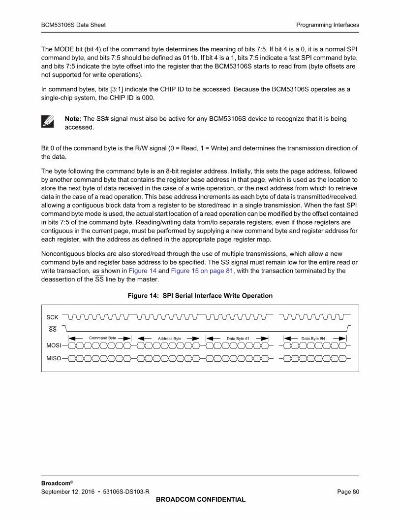
Programming InterfacesBCM53106S Data Sheet
BROADCOM CONFIDENTIAL
Broadcom®
September 12, 2016 • 53106S-DS103-R Page 80
The MODE bit (bit 4) of the command byte determines the meaning of bits 7:5. If bit 4 is a 0, it is a normal SPIcommand byte, and bits 7:5 should be defined as 011b. If bit 4 is a 1, bits 7:5 indicate a fast SPI command byte,and bits 7:5 indicate the byte offset into the register that the BCM53106S starts to read from (byte offsets arenot supported for write operations).
In command bytes, bits [3:1] indicate the CHIP ID to be accessed. Because the BCM53106S operates as asingle-chip system, the CHIP ID is 000.
Bit 0 of the command byte is the R/W signal (0 = Read, 1 = Write) and determines the transmission direction ofthe data.
The byte following the command byte is an 8-bit register address. Initially, this sets the page address, followedby another command byte that contains the register base address in that page, which is used as the location tostore the next byte of data received in the case of a write operation, or the next address from which to retrievedata in the case of a read operation. This base address increments as each byte of data is transmitted/received,allowing a contiguous block data from a register to be stored/read in a single transmission. When the fast SPIcommand byte mode is used, the actual start location of a read operation can be modified by the offset containedin bits 7:5 of the command byte. Reading/writing data from/to separate registers, even if those registers arecontiguous in the current page, must be performed by supplying a new command byte and register address foreach register, with the address as defined in the appropriate page register map.
Noncontiguous blocks are also stored/read through the use of multiple transmissions, which allow a newcommand byte and register base address to be specified. The SS signal must remain low for the entire read orwrite transaction, as shown in Figure 14 and Figure 15 on page 81, with the transaction terminated by thedeassertion of the SS line by the master.
Figure 14: SPI Serial Interface Write Operation
Note: The SS# signal must also be active for any BCM53106S device to recognize that it is beingaccessed.
SCK
SS
MOSI
MISO
Command Byte Address Byte Data Byte #1 Data Byte #N

Programming InterfacesBCM53106S Data Sheet
BROADCOM CONFIDENTIAL
Broadcom®
September 12, 2016 • 53106S-DS103-R Page 81
Figure 15: SPI Serial Interface Read Operation
SCK
SS
MOSI
MISO
Command Byte Address Byte
Data Byte #1 Data Byte #N

Programming InterfacesBCM53106S Data Sheet
BROADCOM CONFIDENTIAL
Broadcom®
September 12, 2016 • 53106S-DS103-R Page 82
Figure 16 shows the typical connection block diagram for SPI interface with/without external PHY devices.
Figure 16: SPI Interface Without External PHY Device
External PHY Registers
The BCM53106S also uses the MDIO/MDC interface for polling registers of an external PHY. In this case, theMDIO/MDC interface polls the external PHY registers pulling the data internal to the BCM53106S. Then, theexternal PHYs and retrieved from the register data using the SPI interface. The MDIO/MDC interface is not usedas a method to access internal PHY registers. This must be done using the SPI interface. In this case, the MDC/MDIO interface of the BCM53106S is acting as a master.
Figure 17: Accessing External PHY Registers
SPI Device
MOSI
SCKSS#
MISOMOSI
SCKSS#
MISO
Master
Slave
RoboSwitch
SwitchSPI
Device
MOSI
SCKSS#
MISOMOSI
SCKSS#
MISO
MasterSlave
SwitchInternal
Registers
Includes Polled Registers of
Ext PHY
RoboSwitch
ExtPHY
MDC MDIO
Slave
External PHY registers are accessed by the SPI comap ble device via the SPI access to the switch registers.
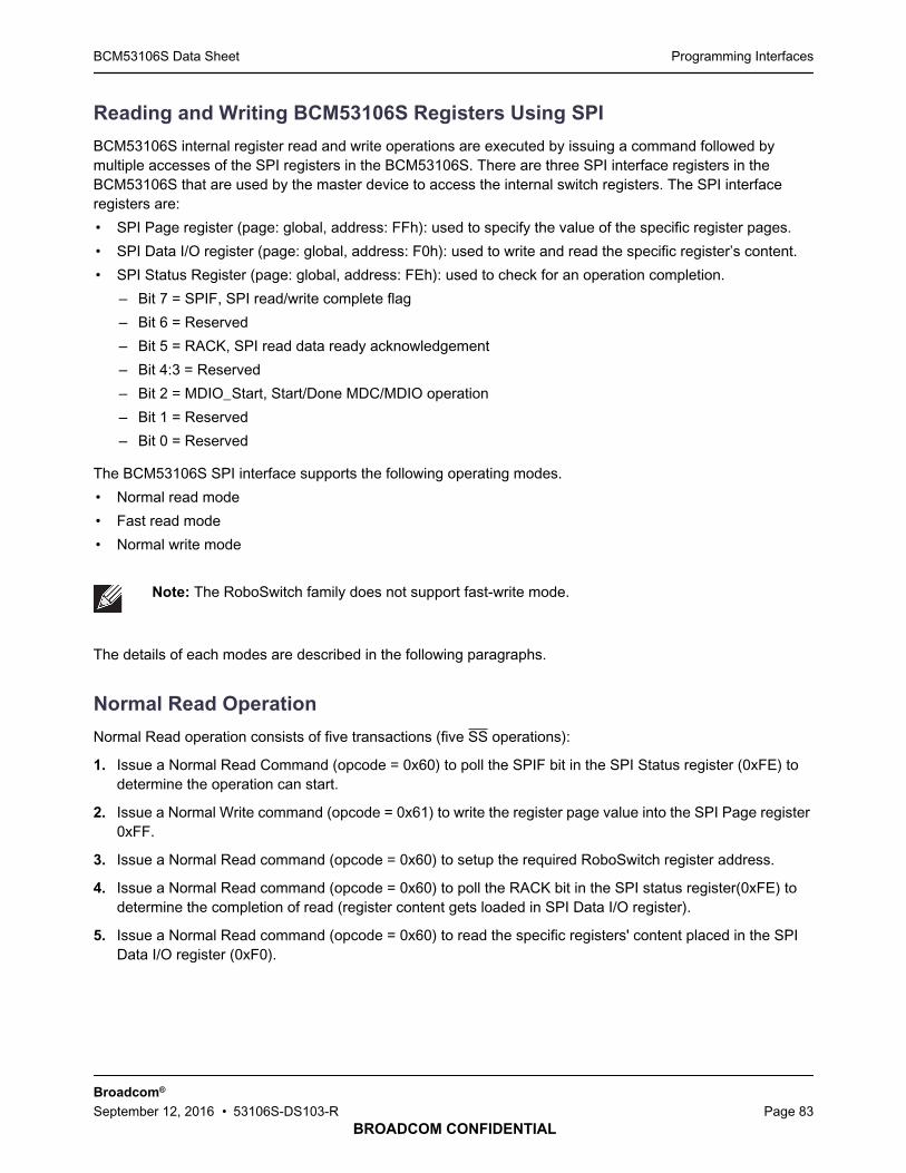
Programming InterfacesBCM53106S Data Sheet
BROADCOM CONFIDENTIAL
Broadcom®
September 12, 2016 • 53106S-DS103-R Page 83
Reading and Writing BCM53106S Registers Using SPI
BCM53106S internal register read and write operations are executed by issuing a command followed bymultiple accesses of the SPI registers in the BCM53106S. There are three SPI interface registers in theBCM53106S that are used by the master device to access the internal switch registers. The SPI interfaceregisters are:
• SPI Page register (page: global, address: FFh): used to specify the value of the specific register pages.
• SPI Data I/O register (page: global, address: F0h): used to write and read the specific register’s content.
• SPI Status Register (page: global, address: FEh): used to check for an operation completion.
– Bit 7 = SPIF, SPI read/write complete flag
– Bit 6 = Reserved
– Bit 5 = RACK, SPI read data ready acknowledgement
– Bit 4:3 = Reserved
– Bit 2 = MDIO_Start, Start/Done MDC/MDIO operation
– Bit 1 = Reserved
– Bit 0 = Reserved
The BCM53106S SPI interface supports the following operating modes.
• Normal read mode
• Fast read mode
• Normal write mode
The details of each modes are described in the following paragraphs.
Normal Read Operation
Normal Read operation consists of five transactions (five SS operations):
1. Issue a Normal Read Command (opcode = 0x60) to poll the SPIF bit in the SPI Status register (0xFE) todetermine the operation can start.
2. Issue a Normal Write command (opcode = 0x61) to write the register page value into the SPI Page register0xFF.
3. Issue a Normal Read command (opcode = 0x60) to setup the required RoboSwitch register address.
4. Issue a Normal Read command (opcode = 0x60) to poll the RACK bit in the SPI status register(0xFE) todetermine the completion of read (register content gets loaded in SPI Data I/O register).
5. Issue a Normal Read command (opcode = 0x60) to read the specific registers' content placed in the SPIData I/O register (0xF0).
Note: The RoboSwitch family does not support fast-write mode.

Programming InterfacesBCM53106S Data Sheet
BROADCOM CONFIDENTIAL
Broadcom®
September 12, 2016 • 53106S-DS103-R Page 84
Figure 18: Normal Read Operation
Example: Read from 100BASE-T Control register (page 10h, offset 12h).
1. Issue a Normal Read command (opcode = 0x60) to check the SPIF bit in the SPI Status register (0xFE).
Normal Read Mode
Start
Step 1
Issue Normal Read Command
(opcode=60) to poll data from
SPI Status Register (0xFE)
SPIF (bit 7) =0?
Step 2
Issue Normal Write Command
(opcode=61) to write the
accessed register page valueinto SPI Page Register (0xFF)
RACK (bit 5) =1?
Step 5
Issue Normal Read Command
(opcode=60) to read data from
SPI Data I/O Register (0xF0) [MSB first, continute if more
bytes]
Yes
Yes
No
No
Done
Is accessed
Register page same as
previous?
Yes
No
Step 4
Issue Normal Read Command
(opcode=60) to poll data from SPI Status Register (0xFE)
Software
Timeout ?
Software
Timeout ?
Task Abort
Yes
No
No
Yes
Issue Normal Write Command
(opcode=61) to write the
accessed register page value
into SPI Page Register (0xFF)
Step 3
Issue Normal Read Command
(opcode=60) to setup the accessed register address

Programming InterfacesBCM53106S Data Sheet
BROADCOM CONFIDENTIAL
Broadcom®
September 12, 2016 • 53106S-DS103-R Page 85
• Assert SS while SCK is high idle state.
• Clock in a Normal Read Command Byte: 0 1 1 0 0 0 0 0 (opcode = 0x60).
• Clock in the SPI Status register address (0xFE).
• Clock out the SPI Status register value: 0 0 0 0 0 0 0 0 (SPIF bit 7 = 0).
• Deassert SS while SCK is high idle state.
Figure 19: Normal Read Mode to Check the SPIF Bit of SPI Status Register
2. Issue a Normal Write command (opcode = 0x61) and write the accessed register page value of 0x10 intoSPI Page Register(0xFF)—this step is required only if previous read/write was not to/from Page 10h.
• Assert SS while SCK is high idle state.
• Clock in a Normal Write Command Byte: 0 1 1 0 0 0 0 1 (opcode = 0x61).
• Clock in offset of Page register (0xFF).
• Clock in the accessed register page value: 0 0 0 1 0 0 0 0 (Page register: 0x10).
• Deassert SS while SCK is high idle state.
Figure 20: Normal Read Mode to Setup the Accessed Register Page Value
3. Issue a Normal Read command (opcode = 0x60) and write the accessed register address value 0x12, andclock out 8 bits to complete the read cycle, but discard result (this is where the state machine triggers ainternal data transfer from Address 0x12 to the SPI Data I/O register).
• Assert SS while SCK is high idle state.
• Clock in a Normal Read Command Byte: 0 1 1 0 0 0 0 0 (opcode = 0x60).
• Clock in the address of accessed register address value (0x12).
• Clock out eight clocks for the dummy read, and discard results on MISO.
• Deassert SS while SCK is high idle state.
SS
SCLK
MOSI
MISO
Command Byte SPI Status
Reg offsetSPI Status Byte
SS
SCLK
MOSI
MISO
Command Byte SPI Page Register
OffsetRegister Page

Programming InterfacesBCM53106S Data Sheet
BROADCOM CONFIDENTIAL
Broadcom®
September 12, 2016 • 53106S-DS103-R Page 86
Figure 21: Normal Read Mode to Setup the Accessed Register Address Value (Dummy Read)
4. Issue a Normal Read command (opcode = 0x60) to read the SPI Status to check the RACK bit for completionof the register content transfer to the SPI Data I/O register. (This step may be repeated until the proper bitset is read.)
• Assert SS while SCK is high idle state.
• Clock in a Normal Read Command Byte: 0 1 1 0 0 0 0 0 (opcode = 0x60).
• Clock in offset for SPI Status Register (0xFE): 1 1 1 1 1 1 1 0.
• Clock out the content of SPI Status bits.
• Repeat the polling until the content of SPI Status Register value: 0 0 1 0 0 0 0 0 (RACK bit 5 = 1).
• Deassert SS while SCK is high idle state.
Figure 22: Normal Read Mode to Check the SPI Status for Completion of Read
5. Issue a Normal Read command (opcode = 0x60) to read the data from the SPI Data I/O register:
• Assert SS while SCK is high idle state.
• Clock in Command Byte: 0 1 1 0 0 0 0 0 (opcode = 0x60).
• Clock in offset of SPI Data I/O Register (0xF0).
• Clock out first data byte on MISO line: 0 0 0 0 0 0 0 0 (byte 0 = bit 7 to bit 0 = MSB to LSB).
• Clock out next byte (in this case, last) on MISO line: 0 0 0 0 1 1 1 0 (byte 1 = bit 15 to bit 8).
• [Continue if more bytes].
• Deassert SS while SCK is high idle state.
–
Note: This dummy read is always eight clock cycles, whether or not it is an 8-bit register.
SS
SCLK
MOSI
MISO
Command ByteRead
Register OffsetDummy Byte
SS
SCLK
MOSI
MISO
Command Byte SPI Status
Reg offsetSPI Status Byte

Programming InterfacesBCM53106S Data Sheet
BROADCOM CONFIDENTIAL
Broadcom®
September 12, 2016 • 53106S-DS103-R Page 87
Figure 23: Normal Read Mode to Obtain the Register Content
Fast Read Operation
Fast Read operation consists of three transactions (three SS operations):
1. Issue a Normal Read Command (opcode = 0x60) to poll the SPIF bit in the SPI Status Register (0xFE) todetermine the operation can start.
2. Issue a Fast Read command (opcode = 0x10) to setup the accessed Register Page value into the Pageregister (0xFF).
3. Issue a Fast Read command (opcode = 0x10) to setup the accessed register address value, to trigger anactual read, and retrieve the accessed register content till the completion.
Fast Read mode process is different from Normal Read mode, once the switch receives a fast read commandfollowed by the register page and address information, the status and the data (register content) will be put onthe MISO line without going through the SPI Status register or SPI Data I/O register. Once RACK bit of the bytesfollowing the Fast Read command with Address information is recognized the register content will be put onMISO line immediately following the byte with RACK bit set. The Fast Read process is described in the followingparagraphs with a flowchart followed by a step by step description.
SS
SCLK
MOSI
MISO
Command Byte SPI Data I /O
Reg offset
Read Data
Byte 1
Read Data
Byte 0

Programming InterfacesBCM53106S Data Sheet
BROADCOM CONFIDENTIAL
Broadcom®
September 12, 2016 • 53106S-DS103-R Page 88
Figure 24: Fast Read Operation
Example: Read from 100BASE-T Control register (page 10h, offset 12h).
Fast Read Mode
Start
SPIF (bit 7) =0?
Yes
No
Step 1
Issue a Normal Read
Command (opcode=60) to poll
data from SPI Status Register
(0xFE)
Issue a Fast Read Command
(opcode=10) to setup the
accessed register address
value to trigger an actual read
Step 2
Issue a Normal Write
Command (opcode=61) to
write the accessed register
page value into SPI Page Register (0xFF)
Is accessed
Register page same as previous?
Yes
No
Software
Timeout ?
No
Yes
NoRACK=1
Retrieve the data starting
from the lowest byte
Yes
Done
Software
Timeout ?
No
Retrieve the first byte data to
check RACK is ready
Yes
Task Abort
Step 3
Issue a Normal Write
Command (opcode=61) to write the accessed register
page value into SPI Page
Register (0xFF)

Programming InterfacesBCM53106S Data Sheet
BROADCOM CONFIDENTIAL
Broadcom®
September 12, 2016 • 53106S-DS103-R Page 89
1. Issue a Normal Read command (opcode = 0x60) to check the SPIF bit in the SPI Status register (0xFE).
• Assert SS while SCK is high idle state.
• Clock in a Normal Read Command Byte: 0 1 1 0 0 0 0 0 (opcode = 0x60).
• Clock in the SPI Status register address (0xFE).
• Clock in the accessed register page value: 0 0 0 0 0 0 0 0 (SPIF bit 7 = 0).
• Deassert SS while SCK is high idle state.
Figure 25: Normal Read Mode to Check the SPIF Bit of SPI Status Register
2. Issue a Normal Write command (opcode = 0x61) and write the accessed register page value of 0x10 in toSPI Page Register(0xFF)—this step is required only if previous read/write was not to/from Page 10h.
• Assert SS while SCK is high idle state.
• Clock in a Fast Read Command Byte: 0 11 0 0 0 0 0 1 (opcode = 0x61).
• Clock in offset of Page register (0xFF).
• Clock in the accessed register page value: 0 0 0 1 0 0 0 0 (Page register: 0x10).
• Deassert SS while SCK is high idle state.
Figure 26: Fast Read Mode to Setup New Page Value
3. Issue a Fast Read command (opcode = 0x10), followed by the Address of the accessed register (0x12),check for a read completion by checking the RACK bit in the SPI Status register, and finally clock out theread data.
• Assert SS while SCK is high idle state.
• Clock in a Fast Read Command Byte: 0 0 0 1 0 0 0 0 0 (opcode = 0x10).
• Clock in the Address of accessed register (0x12).
• Clock out Bytes Until Bit 0 or Bit 1 = 1: 0 0 0 0 0 0 0 1 (RACK bit 0 = 1).
• Clock out first data byte: 0 0 0 0 0 0 0 0 (Byte 0 = Bit 7 to Bit 0).
• Clock out next data (in this case, last) byte = 0 0 0 0 1 1 1 0 (Byte 1 = Bit 15 to Bit 8).
SS
SCLK
MOSI
MISO
Command Byte SPI Status
Reg offsetSPI Status
Byte
SS
SCLK
MOSI
MISO
Command Byte SPI Page Register
OffsetRegister Page

Programming InterfacesBCM53106S Data Sheet
BROADCOM CONFIDENTIAL
Broadcom®
September 12, 2016 • 53106S-DS103-R Page 90
• [Continue if more bytes].
• Deassert SS while SCK is high idle state.
Figure 27: Fast Read to Read the Register
Normal Write Operation
Normal Write operation consists of three transactions (three SS operations):
1. Issue a Normal Read Command (opcode = 0x60) to poll the SPIF bit in the SPI Status register (0xFE) todetermine the operation can start.
2. Issue a Normal Write command (opcode = 0x61) to setup the accessed register page value into the pageregister (0xFF).
3. Issue a Normal Write command (opcode = 0x61) to setup the accessed register address value, followed bythe write content starting from a lower byte.
The Normal Write Mode process is described in the following paragraphs with a flowchart followed by a step bystep description.
Note: There is an errata on the RACK output timing in Fast Read mode. The RACK (bit 0) must besampled prior to toggling the clock to shift out the bit 0.
Note: The RoboSwitch does not support Fast Write Mode.
SS
SCLK
MOSI
MISO
Command Byte Read
Register Offset
RACK bit
= 1 ?
Read Data Byte 1Read Data Byte 0
See the note below !

Programming InterfacesBCM53106S Data Sheet
BROADCOM CONFIDENTIAL
Broadcom®
September 12, 2016 • 53106S-DS103-R Page 91
Figure 28: Normal Write Operation
Example: 0x1600h is written to 100BASE-T Control register (page 0x10, offset 0x12).
1. Issue a Normal Read command (opcode = 0x60) to check the SPIF bit in the SPI Status register (0xFE).
• Assert SS while SCK is high idle state.
• Clock in a Normal Read Command Byte = 0 1 1 0 0 0 0 0 (opcode = 0x60).
• Clock in the SPI Status register address (0xFE).
• Clock in the accessed register page value = 0 0 0 0 0 0 0 0 (SPIF bit 7=0).
• Deassert SS while SCK is high idle state.
Start
Step 1
Command
data from SPI
SPIF=0?
Step 2
Issue a Normal Write Command (opcode=61) to
write the accessed register
page value into SPI Page
Register (0xFF)
Step 3
Done
Normal Write Mode
No
Yes
Is accessed
register page same as
previous?
Yes
No
Software
Timeout ?
Issue a Normal Write
Command (opcode=61) to
write the accessed register
page value into SPI Page
Register (0xFF)
Task Abort
Yes
No
Issue a Normal Read
Command (opcode=60)
to poll data from SPI
Status Register (0xFE)
Issue a Normal Write
Command (opcode=61) to
setup the accessed register
address, followed by the write
content starting from the
lowest byte
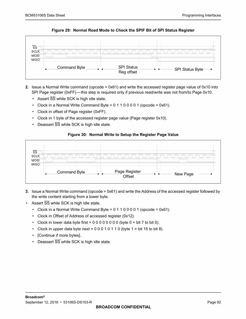
Programming InterfacesBCM53106S Data Sheet
BROADCOM CONFIDENTIAL
Broadcom®
September 12, 2016 • 53106S-DS103-R Page 92
Figure 29: Normal Read Mode to Check the SPIF Bit of SPI Status Register
2. Issue a Normal Write command (opcode = 0x61) and write the accessed register page value of 0x10 intoSPI Page register (0xFF)—this step is required only if previous read/write was not from/to Page 0x10.
• Assert SS while SCK is high idle state.
• Clock in a Normal Write Command Byte = 0 1 1 0 0 0 0 1 (opcode = 0x61).
• Clock in offset of Page register (0xFF).
• Clock in 1 byte of the accessed register page value (Page register 0x10).
• Deassert SS while SCK is high idle state.
Figure 30: Normal Write to Setup the Register Page Value
3. Issue a Normal Write command (opcode = 0x61) and write the Address of the accessed register followed bythe write content starting from a lower byte.
• Assert SS while SCK is high idle state.
• Clock in a Normal Write Command Byte = 0 1 1 0 0 0 0 1 (opcode = 0x61).
• Clock in Offset of Address of accessed register (0x12).
• Clock in lower data byte first = 0 0 0 0 0 0 0 0 (byte 0 = bit 7 to bit 0).
• Clock in upper data byte next = 0 0 0 1 0 1 1 0 (byte 1 = bit 15 to bit 8).
• [Continue if more bytes].
• Deassert SS while SCK is high idle state.
SS
SCLK
MOSI
MISO
Command Byte SPI Status
Reg offsetSPI Status Byte
SS
SCLK
MOSI
MISO
Command Byte Page Register
Offset
New Page

Programming InterfacesBCM53106S Data Sheet
BROADCOM CONFIDENTIAL
Broadcom®
September 12, 2016 • 53106S-DS103-R Page 93
Figure 31: Normal Write to Write the Register Address Followed by Written Data
EEPROM Interface
The BCM53106S can be connected using the serial interface to a low-cost external serial EEPROM, enablingit to download register-programming instructions during power-on initialization. For each programminginstruction fetched from the EEPROM, the instruction executes immediately and affects the register file.
During the chip-initialization phase, the switch identifies automatically the type of EEPROM it is connected to,then the data is sequentially read-in from the EEPROM after the internal memory has been cleared. The firstdata read-in is the HEADER and it matches a predefined magic code. In the case where the HEADER data doesnot match the instruction fetch, the process stops, and the EEPROM controller treats it as if no EEPROM exists.If the magic code matches, the fetch instruction process continues until it reaches the instruction length definedin the HEADER.
Figure 32: Serial EEPROM Connection
EEPROM Format
The EEPROM should be configured to x16 word format. The header contains key and length information asshown in Table 21 on page 94. The actual data stored in the EEPROM is byte-swapped as shown in Table 22on page 94.
• Upper 5 bits are magic code 15h, which indicates that valid data follows.
• Bit 10 is for speed indication. A 0 means normal speed. A 1 indicates speedup. The default is 0.
• Lower 10 bits indicate the total length of all entries. For example:
– 93C46 up to 64 words
– 93C56 up to 128 words
– 93C66 up to 256 words
– 93C86 up to 1024 words
SS
SCLK
MOSI
MISO
Command Byte Register
OffsetWrite Data Byte 1Write Data Byte 0
SS
SCK
MOSI
MISO
BCM53134x 93C46/56/66/86
CS
SK
DI
DO

Programming InterfacesBCM53106S Data Sheet
BROADCOM CONFIDENTIAL
Broadcom®
September 12, 2016 • 53106S-DS103-R Page 94
Figure 33 shows an EEPROM programming example.
Figure 33: EEPROM Programming Example
Table 21: EEPROM Header Format
Bits [15:11} Bit 10 Bits [9:0]
Magic code, 15h Speed Total entry number93C46: 0 to 6393C56: 0 to 12793C66: 0 to 25593C86: 0 to 1023
Table 22: EEPROM Contents
Bits [7:0] Bits [15:11] Bit 10 Bits [9:8]
Total entry number Magic code, 15h Speed Total entry number
101010101
FF 01
00 02
06 01
43 21
.
...
00
01
02
03
04
05
07
08
.
.
3F
0715
MC : TOTAL ENTRY NUM
22 1106
0 000010
56
66
Address FF’h (Page)
Data 01'h
MC : 101010101
101010001
FF 01
00 10
30 01
01 3C
FF 01
30
.
...
00
01
02
03
04
05
07
08
.
.
3F
0715
TOTAL ENTRY NUM
00 1106
0 000000Write
Page:10'h Offset :30'h Data:013C’h
Page:11'h Offset :30'h Data:013C’h
56
01 3C
Data Entry Num . # 01
Data 3C'h
Page # 10'h
A890
FF01
0010
3001
EEPROM Serial Stream: 90 A8 01 FF 10 00 01 30 3C 01 01 FF 11 00 01 30 3C 01
Page # 00'h
Offset 30’h Data Entry Num . # 01
Address FF’h (Page)01
Page # 11'hPage # 00'h
Data 01'h Data 3C'h
Offset 30’h Data Entry Num . # 01
013C
FF01
0011
3001
013C
Data Entry Num . # 01
S : 0 (Normal) : 08 'h

Programming InterfacesBCM53106S Data Sheet
BROADCOM CONFIDENTIAL
Broadcom®
September 12, 2016 • 53106S-DS103-R Page 95
Serial Flash Interface
The BCM53106S offers a serial flash interface to store program code for the internal microcontroller (BCM8051processor). The BCM53106S detects a flash memory device automatically and downloads the memory contentsupon power-up. The main purpose of the stored code is to configure and run the power savings mode, such asany application that the user wishes to run that can fit in the internal BCM8051 memory. The embeddedBCM8051 microcontroller has 32 KB of SRAM and 16 KB of ROM. The interface comprises four signal pins:chip select (FCS), Flash clock (FCLK), Flash Serial Out (FSO), and Flash Serial In (FSI). The maximumfrequency of the interface is 25 MHz.
MDC/MDIO Interface
The BCM53106S offers an MDC/MDIO interface for accessing the switch registers as well as the PHY registers.An external management entity can access the switch registers through this interface when the SPI interface isnot used. (when the SPI clock is in idle mode.) The switch registers are accessed through the Pseudo PHYinterface, and the PHY registers are accessed directly by using direct PHY addresses from 0x00 ~ 0x04 (i.e.,the PHYs are mapped to Register page 0x10 ~ 0x14 when it is accessed through the SPI interface).
An external PHY can be connected to the GMII interface of the IMP port and Port 5. Through the SPI interface,by accessing the Page 88h and Page 85h, the external PHY MII registers can be accessed.
MDC/MDIO Interface Register Programming
The BCM53106S are designed to be fully compliant with the MII clause of the IEEE 802.3u Ethernetspecification. The MDC pin of the BCM53106S sources a 2.5 MHz clock. Serial bidirectional data transmittedusing the MDIO pin is synchronized with the MDC clock. Each MII read or write instruction is initiated by theBCM53106S and contains the following:
• Preamble (PRE). To signal the beginning of an MII instruction after reset, at least 32 consecutive 1-bitsmust be written to the MDIO pin. A preamble of 32 1-bits is required only for the first read or write followingreset. A preamble of fewer than 32 1-bits causes the remainder of the instruction to be ignored.
• Start of Frame (ST). A 01 pattern indicates that the start of the instruction follows.
• Operation Code (OP). A read instruction is indicated by 10, while a write instruction is indicated by 01.
• PHY Address (PHYAD). A 5-bit PHY address follows, with the MSB transmitted first. The PHY addressallows a single MDIO bus to access multiple PHY chips.
• Register Address (REGAD). A 5-bit register address follows, with the MSB transmitted first.
• Turnaround (TA). The next bit times are used to avoid contention on the MDIO pin when a read operationis performed. When a write operation is being performed, 10 must be sent by the BCM53106S chip duringthese two bit times. When a read operation is being performed, the MDIO pin of the BCM53106S must beput in a high-impedance state during these bit times. The external PHY drives the MDIO pin to 0 during thesecond bit time.
• Data. The last 16 bits of the Instruction are the actual data bits. During a write operation, these bits arewritten to the MDIO pin with the most significant bit (MSB) transmitted first by the BCM53106S. During aread operation, the data bits are driven by the external PHY with the MSB transmitted first.
Note: The PHY registers are not accessible through the Pseudo PHY operation.

Programming InterfacesBCM53106S Data Sheet
BROADCOM CONFIDENTIAL
Broadcom®
September 12, 2016 • 53106S-DS103-R Page 96
Pseudo-PHY
The MDC/MDIO can be used by an external management entity to read/write register values internal to theBCM53106S. This mode offers an alternative programming interface to the chip. The BCM53106S operate inslave mode with a PHY address of 30d. The following figures show the register setup flow chart for accessingthe registers using the MDC/MDIO interface.
Figure 34: Pseudo-PHY MII Register Definitions
IEEE Reserved
Page Number Reserved A
Register Address Reserved OP
Access Status
Reserved
Reserved
Access register bits [15:0]
Access register bits [31:16]
Access register bits [47:32]
Access register bits [63:48]
Reg 0
Reg 15
Reg 16
Reg 17
Reg 18
Reg 24
Reg 25
Reg 26
Reg 27
Reg 31

Programming InterfacesBCM53106S Data Sheet
BROADCOM CONFIDENTIAL
Broadcom®
September 12, 2016 • 53106S-DS103-R Page 97
Figure 35: Pseudo-PHY MII Register 16: Register Set Access Control Bit Definition
Figure 36: Pseudo-PHY MII Register 17: Register Set Read/Write Control Bit Definition
Figure 37: Pseudo-PHY MII Register 18: Register Access Status Bit Definition
Note: The bit 0 (MDC/MDIO Access Enable) in register 16 should be released (set to 0) after atransaction is completed. This allows the SPI interface to access the switch register if required.
Page Number Reserved A Reg 16
15 14 13 12 11 10 9 8 7 6 5 4 3 2 1 0 Bit #
bits [15:8] => Page number (RW)bits [71] => ReservedBit 0 => Register set MDC/MDIO access enable (RW)
Register Address Reserved OP Reg 17
15 14 13 12 11 10 9 8 7 6 5 4 3 2 1 0 Bit #
bits [15:8] => Register address (RW)bits [7:2] => Reservedbits [1:0] => OP code (RW/SC),00 = No operation
01 = Write operation10 = Read operation11 = Reserved
Reserved P Reg 18
15 14 13 12 11 10 9 8 7 6 5 4 3 2 1 0 Bit #
bits [15:1] => ReservedBit 1 => Operation Error (RO/LH), when op_code = 2'b11, this bit is set to show operation error.Bit 0 => Prohibit Access (RO/LH), for Page Number = 8'h1X, which are PHY MII registers.
E

Programming InterfacesBCM53106S Data Sheet
BROADCOM CONFIDENTIAL
Broadcom®
September 12, 2016 • 53106S-DS103-R Page 98
Figure 38: Pseudo-PHY MII Register 24: Access Register Bit Definition
Figure 39: Pseudo-PHY MII Register 25: Access Register Bit Definition
Figure 40: Pseudo-PHY MII Register 26: Access Register Bit Definition
Access register bits [15:0] Reg 24
15 14 13 12 11 10 9 8 7 6 5 4 3 2 1 0 Bit #
bits [15:0] => Access register bits [15:0] (RW)
Access register bits [31:16] Reg 25
15 14 13 12 11 10 9 8 7 6 5 4 3 2 1 0 Bit #
bits [15:0] => Access register bits [31:16] (RW)
Access register bits [47:32] Reg 26
15 14 13 12 11 10 9 8 7 6 5 4 3 2 1 0 Bit #
bits [15:0] => Access register bits [47:32] (RW)

Programming InterfacesBCM53106S Data Sheet
BROADCOM CONFIDENTIAL
Broadcom®
September 12, 2016 • 53106S-DS103-R Page 99
Figure 41: Pseudo-PHY MII Register 27: Access Register Bit Definition
Access register bits [63:48] Reg 27
15 14 13 12 11 10 9 8 7 6 5 4 3 2 1 0 Bit #
bits [15:0] => Access register bits [63:48] (RW)

Programming InterfacesBCM53106S Data Sheet
BROADCOM CONFIDENTIAL
Broadcom®
September 12, 2016 • 53106S-DS103-R Page 100
Figure 42: Read Access to the Register Set using the Pseudo-PHY (PHYAD = 11110) MDC/MDIO Path
Write MII register 16:Set bit 0 as 1
Set Page Number to bits [15:8]
Write MII register 17:Set Operation Code as 10
Set register address to bits [15:8]
Read MII register 24:for Access register bits [15:0]
Read MII register 17:Check op_code = 00?
Read MII register 25:for Access register bits [31:16]
Read MII register 26:for Access register bits [47:32]
Read MII register 27:for Access register bits [63:48]
No
Yes
Yes
New Page Access?
No
No

Programming InterfacesBCM53106S Data Sheet
BROADCOM CONFIDENTIAL
Broadcom®
September 12, 2016 • 53106S-DS103-R Page 101
Figure 43: Write Access to the Register Set using the Pseudo-PHY (PHYAD = 11110) MDC/MDIO Path
Write MII register 16:Set bit 0 as 1
Set Page Number to bits [15:8]
Read MII register 17:Check op_code = 00?
Write MII register 25:for Access register bits [31:16]
Write MII register 26:for Access register bits [47:32]
Write MII register 27:for Access register bits [63:48]
Yes
Yes
New Page Access?
No
No
Write MII register 24:for Access register bits [15:0]
Write MII register 17:Set Operation Code as 01
Set register address to bits [15:8]

LED InterfacesBCM53106S Data Sheet
BROADCOM CONFIDENTIAL
Broadcom®
September 12, 2016 • 53106S-DS103-R Page 102
Table 23 summarizes the complete management frame format.
See “MDC/MDIO Interface” on page 95 for more information regarding the timing requirements.
LED Interfaces
The BCM53106S provides flexible, programmable per-port status of various functions. The user can selectpredefined LED displays per port by setting the LED_MODE strap pins. Or, the user can program differentdisplay functions and different sets of display functions for different ports by programming the LED Controlregisters. Normally the BCM53106S offers a total of 16 LED displays with four functions per port when the WAN(port 5) RGMII interface is not used, or a total of eight LED displays with two functions per port when the WAN(port 5) RGMII interface is used. The LED interface offers options to display different functions.
The options that are available for the LED display include the following:
• Number of displays per port
• Display functions per port
• LED lighting behavior
The total number of displays per port is based on the GMII_LED_DEL strap-pin option. When the GMII (port 5)is used, the 16-LED display option is not available. The LED[xx] signal allocation for each port is shown inTable 24: “8-LED Display Mode (GMII_SEL_LED=0),” on page 103.
The options for the number of LED displays are as follows:
• 16 LED displays total (GMII_LED_SEL = 1)
• Four display functions per port
• LED[0:9] active state will be depends on the strap pin state. The LED active state will follow the same asthe strap state. (i.e., if the strap pin is pulled up, LED active state is high, and vice versa)
• LED[10:15] active state is high. These LED pins will be always active-high, regardless of external/internal pull up or pull down.
• Eight LED displays total (GMII_LED_SEL = 0). This mode is forced when GMII (port 5) is used for datainterface.
• Two display functions per port
• LED[0:7] active state depends on the strap pin state. The LED active state will follow the same as thestrap state. (i.e., if the strap pin is pulled up, the LED active state is high. If the strap pin is pulled low, theLED active state is low.)
The options for the different function displays per port are as follows:
• Using default display settings through the strap pins LED_MODE[1:0].
Table 23: MII Management Frame Format
Operation PRE ST OP PHYAD REGAD TA Data Direction
Read 1 ... 1 01 10 AAAAA RRRRR ZZZ0
Z ... ZD ... D
Driven by masterDriven by slave
Write 1 ... 1 01 01 AAAAA RRRRR 10 D ... D Driven to master

LED InterfacesBCM53106S Data Sheet
BROADCOM CONFIDENTIAL
Broadcom®
September 12, 2016 • 53106S-DS103-R Page 103
• The different displays per LED_MODE settings are shown in Table 24. Each LED [xx] signal is assignedto a specific port. For example, if the port 3 and port 2 LED displays are disabled (register Page 00h,Address 16h = 0003), port 0 and port 1 LED display are still from LED pins LED[0~3] (port 0), LED[4~7](port 1), just as if all four ports were used. If port 1 and port 0 LED displays are disabled (register Page00h, Address 16h = 001C), port 2 and port 3 are still from LED pins LED[8~11] (port 2), and LED[12~15](port 3), also just as if all four ports were used.
• All the ports are displaying a same set of functions based on the strap pin settings. The display is fixedper port and per pin as shown in Table 24.
• Displaying one of two different display settings through programming the LED configuration registers.
• Option to enable LED display per port (register Page 00h, Address 16h).
• There are two sets of displays options the user can set through the LED Function Control Register 0and 1 (register Page 00h, Address 10h, and 12h).
• Each port can select one of two display functions (register Page 00h, Address 14h).
The options for different LED lighting behavior (register Page 00h, Address 18h, and 1Ah) are as follows:
• Automatic mode: All the modes indication is in a steady state, except the activity state, which is blinking.
• Blink mode: All the status indication is blinking. The blinking rate can be set through the register page 00h,address 0Fh, bit [2:0].
• ON mode: Forces the LED to be on.
In serial LED pins, the status of the enabled ports is sent out with the highest port number first with the lowestport number last. Within a port, the highest (in terms of bit number) selected functionality in LED FunctionControl Register 0/1 is sent out first followed by lower (in terms of bit number) selected functionality in LEDFunction Control Register 0/1.
For parallel LED pins, lower ports are mapped to lower LED pins. Port0 is mapped to the lowest LED pins(LED[3:0] or LED[1:0] depending on 16-bit LED or 8-bit LED mode). Port1 is mapped to LED[7:4] or LED[3:2](depending on 16-bit or 8-bit LED mode). Within a port, the lower (in terms of bit number) selected functionalityis LED function Control Register 0/1 is mapped to lower LED pin.
Table 24: 8-LED Display Mode (GMII_SEL_LED=0)
Port 0 Port 1 Port 2 Port 3LED_MODE=2'b11 2’b10 2’b01 2’b00
LED[1] LED[3] LED[5] LED[7] N/A N/A N/A N/A
LED[0] LED[2] LED[4] LED[6] 100M/ACT SPD100M 10_100/ACT SPD100M
Table 25: 16-LED Display Mode (WANLEDSEL=1)
Port 0 Port 1 Port 2 Port 3LED_MODE=2'b11 2’b10 2’b01 2’b00
LED[3] LED[7] LED[11] LED[15] N/A N/A N/A N/A
LED[2] LED[6] LED[10] LED[14] 100M/ACT SPD100M 10_100/ACT SPD100M
LED[1] LED[5] LED[9 LED[13] 10M/ACT LNK/ACT DPX/COL NK/ACT
LED[0] LED[4] LED[8] LED[12] DPX DPX PHYLED4 PHYLED4

LED InterfacesBCM53106S Data Sheet
BROADCOM CONFIDENTIAL
Broadcom®
September 12, 2016 • 53106S-DS103-R Page 104
Figure 44 on page 104 shows the LED Interface register structure.
Figure 44: LED Interface Register Structure Diagram
The BCM53106S offers two LED Interfaces: a parallel LED interface and a serial interface. As shown inFigure 45 on page 105, the source of the LED status stream is the same for both interfaces. The status bitstream is based on the programmed register settings. The Parallel LED Interface provides all the shifting andstoring of the status internally so that it does not require any external shift registers, but it requires more I/O pinsto be connected on the part. The active level of the LED DATA signal can be low or high, depending on the strappin configuration of each LED signal in the parallel LED interface output. The determination of the active stateis shown in “Dual Input Configuration/LED Output Function” on page 106.
LED Function Control Register 0
Selected FunctionsAvailable Functions
Reserved
Reserved
Reserved
LED Function Map Register
LED Enable Map Register
Port Mode Map 0 Register 0 1 0 1
Port Mode Map 1 Register 0 0 1 1
Port / Bit # 3 2 1 0
1 1 0 0
1 1 0 0
1 0 1 1
1 1 0 0
15 : PHYLED3
14 : BroadSync HD Link
13 : —
12 : 10/100M/ACT
11 : 100M/ACT
10 : 10M/ACT
9 : —
8 : SPDI00M
7 : SPD10M
6 : DPX/COL
5 : LNK/ACT
4 : COL
3 : ACT
2 : DPX
1 : LNK
0 : PHYLED4
LED Function Control Register 1
Selected FunctionsAvailable Functions
15 : PHYLED3
14 : BroadSync HD Link
13 : —
12 : 10/100M/ACT
11 : 100M/ACT
10 : 10M/ACT
9 : —
8 : SPDI00M
7 : SPD10M
6 : DPX/COL
5 : LNK/ACT
4 : COL
3 : ACT
2 : DPX
1 : LNK
0 : PHYLED4
1G/ACT
LNKL/ACTG
DPX/COL
LNK LNKG/ACTL
SPD100M
LED OFFLED ON
LED BLINK
LED AUTO
Note:
PHYLED3 and PHYLED4 are the output of the
functions that are selected in the LED Selector 2
Register (Page10h– 14h: Address 38P Shadow
value 01110'b)
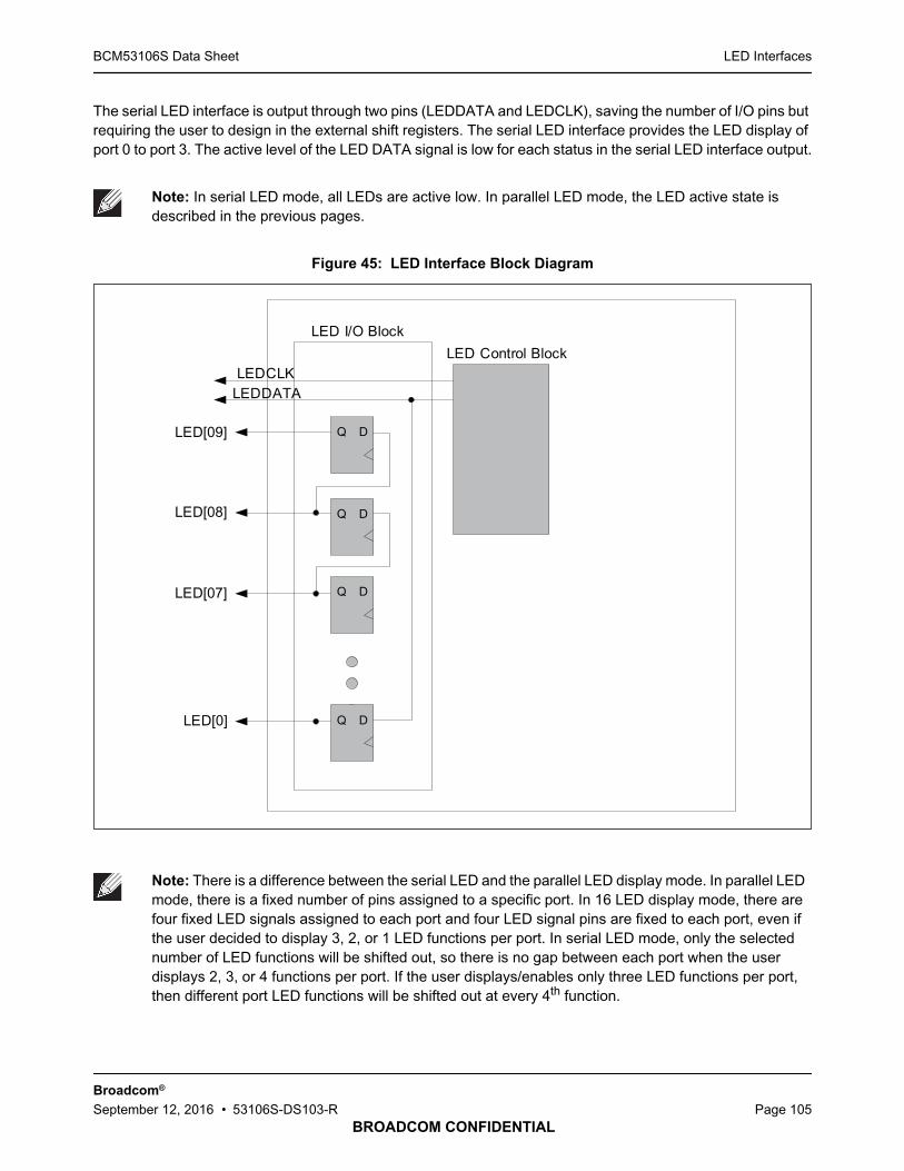
LED InterfacesBCM53106S Data Sheet
BROADCOM CONFIDENTIAL
Broadcom®
September 12, 2016 • 53106S-DS103-R Page 105
The serial LED interface is output through two pins (LEDDATA and LEDCLK), saving the number of I/O pins butrequiring the user to design in the external shift registers. The serial LED interface provides the LED display ofport 0 to port 3. The active level of the LED DATA signal is low for each status in the serial LED interface output.
Figure 45: LED Interface Block Diagram
Note: In serial LED mode, all LEDs are active low. In parallel LED mode, the LED active state isdescribed in the previous pages.
Note: There is a difference between the serial LED and the parallel LED display mode. In parallel LEDmode, there is a fixed number of pins assigned to a specific port. In 16 LED display mode, there arefour fixed LED signals assigned to each port and four LED signal pins are fixed to each port, even ifthe user decided to display 3, 2, or 1 LED functions per port. In serial LED mode, only the selectednumber of LED functions will be shifted out, so there is no gap between each port when the userdisplays 2, 3, or 4 functions per port. If the user displays/enables only three LED functions per port,then different port LED functions will be shifted out at every 4th function.
Q D
Q D
Q D
LEDCLK
LEDDATA
LED[09]
LED[08]
LED[07]
LED Control Block
LED I/O Block
Q DLED[0]

LED InterfacesBCM53106S Data Sheet
BROADCOM CONFIDENTIAL
Broadcom®
September 12, 2016 • 53106S-DS103-R Page 106
A dual LED is used for displaying more than one status using one LED cell. By packing two different-coloredLEDs into one holder, a dual LED can display more than two states in one cell. Figure 46 shows typical dualLED usage. The green LED displays LNKG/ACT status, while the yellow LED displays LNKF/ACT status.
Figure 46: Dual LED Usage Example
Dual Input Configuration/LED Output Function
There are 10 LED pins that have secondary functions. These pins serve as input pins during the power-on/resetsequence. The logic level of the pin is sampled at reset and configures the secondary function. After the resetprocess is completed, the pin acts as an output LED during normal operation. The polarity of the output LED isdetermined based on the latched input value at reset. For example, if the value at the pin is high during reset,the LED output during normal operation is active-high. The user must first decide, based on the individualapplication, the values of the input configuration pin shown in Table 26 to provide the correct deviceconfiguration. The LED circuit must then be configured to accommodate either an active-low or active-high LEDoutput.
Table 26: Input Configuration/LED Output Function
LED Output Pins Input Configuration PinsInternal Default Pull-up and Pull-downs Active State
LED[0] – Pull-down Same as strap pin state
LED[1] SKIp_RAM_BIST Pull-up Same as strap pin state
LED[2] IMP_VOL_SEL Pull-down Same as strap pin state
LED[3] CLKFREQ[1] Pull-up Same as strap pin state
LED[4] WAN MODE Pull-down Same as strap pin state
LED[5] – Pull-down Same as strap pin state
LED[6] IMP MODE Pull-down Same as strap pin state
LED[7] – Pull-down Same as strap pin state
LED[8] CPU_EEPROM_SEL Pull-up Same as strap pin state
LED[9] HW_FWDG_EN Pull-up Same as strap pin state
Note: For LEDs whose Active State is same as strap pin state only, if the signal is pulled up/down, theLED is active high/low.
LNKF/ACT LNKG/ACTGreen LED
Yellow LED
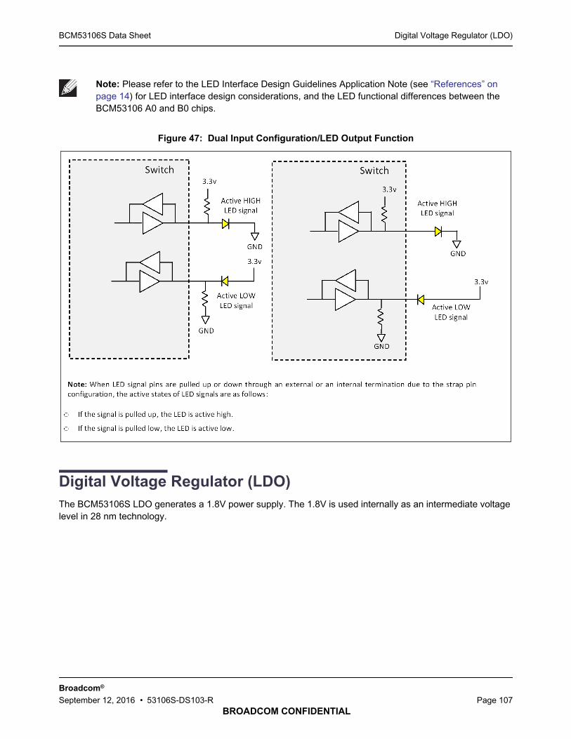
Digital Voltage Regulator (LDO)BCM53106S Data Sheet
BROADCOM CONFIDENTIAL
Broadcom®
September 12, 2016 • 53106S-DS103-R Page 107
Figure 47: Dual Input Configuration/LED Output Function
Digital Voltage Regulator (LDO)
The BCM53106S LDO generates a 1.8V power supply. The 1.8V is used internally as an intermediate voltagelevel in 28 nm technology.
Note: Please refer to the LED Interface Design Guidelines Application Note (see “References” onpage 14) for LED interface design considerations, and the LED functional differences between theBCM53106 A0 and B0 chips.

Hardware Signal DefinitionsBCM53106S Data Sheet
BROADCOM CONFIDENTIAL
Broadcom®
September 12, 2016 • 53106S-DS103-R Page 108
Section 5: Hardware Signal Definit ions
I/O Signal Types
The following conventions are used to identify the I/O types. The I/O pin type is useful in referencing the DC pincharacteristics.
Table 27: I/O Signal Type Definitions
Abbreviation Description
XYZ Active-low signal
3T 3.3V tolerant
A Analog pin type
B Bias pin type
CS Continuously sampled
D Digital pin type
DNC Do not connect
GND Ground
I Input
I/O Bidirectional
IPU Input with internal pull-up
O3S Tristated signal
ODO Open-drain output
O Output
PD Internal pull-down
SOR Sample on reset
PWR Power pin supply
PU Internal pull-up
XT Crystal pin type
Signal DescriptionsBCM53106S Data Sheet
BROADCOM CONFIDENTIAL
Broadcom®
September 12, 2016 • 53106S-DS103-R Page 109
Signal Descriptions
Table 28: Signal Descriptions
Signal Name
Type &DefaultState Description
PHY Interface
TDP0_0 Bi TDP[port#]_[ch#], TDN[port#]_[ch#] are Transmit/Receive Pairs. nTRP/N [port number]_[channel number] for 100BASE-T mode,differential data from the media is transmitted and received on all foursignal pairs. In autonegotiation and 10BASE-T and 100BASE-TXmodes, the BCM53106S normally transmits on TRP/N[port #]_[0] andreceives on TRD[port#]_[1].
TDN0_0 Bi
TDP0_1 Bi
TDN0_1 Bi
TDP1_0 Bi
TDN1_0 Bi
TDP1_1 Bi
TDN1_1 Bi
TDP2_0 Bi
TDN2_0 Bi
TDP2_1 Bi
TDN2_1 Bi
TDP3_0 Bi
TDN3_0 Bi
TDP3_1 Bi
TDN3_1 Bi
RESET/Clock
RESET_L I, Pu Hardware Reset Input. Active low Schmitt-triggered input. Resets theBCM53106S. Active low.
XTAL_P I 50 MHz Crystal Oscillator Input/Output. A continuous 50 MHzreference clock must be supplied to the BCM53106S by connecting a 50MHz crystal between these two pins or by driving XTALI with an clock.When using a crystal, connect a loading capacitor from each pin toexternal 50 MHz oscillator GND.Note: BCM53106 (A0) supports 50 MHz crystal reference clock inputonly.Note: BCM53106 (B0) supports both 25 MHz and 50 MHz crystalreference clock inputs by using the “CLKREF_SEL” strap pin to selectthe state. CLKREF_SEL is shared with the LED5 pin.
XTAL_N I

Signal DescriptionsBCM53106S Data Sheet
BROADCOM CONFIDENTIAL
Broadcom®
September 12, 2016 • 53106S-DS103-R Page 110
Note:
1. The BCM53106 A0 chip only supports a 50 MHz crystal reference clock input.
2. The BCM53106 B0 chip supports both 25 MHz and 50 MHz crystal reference clock inputs by selecting thestrap pin CLKREF_SEL state. The strap pin CLKREF_SEL is shared with the LED5 pin.
IMP Interface
IMP_RXCLK In, Pd IMP port RGMII Interface Receive Clock 125 MHz for 1000 Mbpsoperation, 25 MHz for 100 Mbps operation and 2.5 MHz for 10 Mbpsoperation.
IMP_RXD_0 I, Pd IMP port RGMII Receive Data Inputs. For 1000 Mbps operation, data bitsRXD[3:0] are clocked-out on the rising edge of RXCLK, and data bitsRXD[7:4] are clocked on the falling edge of RXCLK. In 10 Mbps and 100Mbps modes, data bits RXD[3:0] are clocked on the rising edge ofRXCLK.
IMP_RXD_1 I, Pd
IMP_RXD_2 I, Pd
IMP_RXD_3 I, Pd
IMP_RXDV I, Pd IMP port Receive Data Valid. Active high. Indicates the data on theRXD[3:0] pins are encoded and transmitted. Connects to the TXEN ofthe external MAC/Management entity.
IMP_TXCLK O, Pd IMP Port RGMII Transmit Clock. This clock is driven to synchronize thetransmit data in RGMII mode (125 MHz for 1000 Mbps operation, 25MHz for 100 Mbps operation, and 2.5 MHz for 10 Mbps operation). InRGMII mode, both edges of the clock are used to align with TXD[3:0].
IMP_TXD_0 O, Pd IMP Port RGMII Transmit Data Output. For 1000 Mbps operation, databits TXD[3:0] are clocked on the rising edge of TXCLK, and data bitsTXD[7:4] are clocked on the falling edge of TXCLK. For 10 Mbps and100 Mbps, data bits TXD[3:0] are clocked on the rising edge of TXCLK.These output pins have internal 25 series termination resistor.
IMP_TXD_1 O, Pd
IMP_TXD_2 O, Pd
IMP_TXD_3 O, Pd
IMP_TXEN O, Pd
IMP_VOL_REF – Reference point
WAN Port Interface
WAN_RXCLK I, Pd RGMII Receive Clock 125 MHz for 1000 Mbps operation, 25 MHz for100 Mbps operation and 2.5 MHz for 10 Mbps operation.
WAN_RXD0 I, Pd WAN Receive Data Input.
WAN_RXD1 I, Pd
WAN_RXD2 I, Pd
WAN_RXD3 I, Pd
WAN_RXDV I, Pd RGMII/MII Receive Data Valid
LED15_WAN_TXCLK O, Pd When WANLEDSEL = 1b'0: LED15_WAN_TXCLK is used as WANtransmit clock.When WANLEDSEL = 1b'1: LED15_WAN_TXCLK is used as LED15and the polarity is always active low.
Table 28: Signal Descriptions (Cont.)
Signal Name
Type &DefaultState Description

Signal DescriptionsBCM53106S Data Sheet
BROADCOM CONFIDENTIAL
Broadcom®
September 12, 2016 • 53106S-DS103-R Page 111
LED10_WAN_TXD0 O, Pd When WANLEDSEL = 1b'0: LED10_WAN_TXD0 is used as WANtransmit data output 0.When WANLEDSEL = 1b'1: LED10_WAN_TXD0 is used as LED10 andthe polarity is always active low.
LED11_WAN_TXD1 O, Pd When WANLEDSEL = 1b'0: LED11_WAN_TXD1 is used as WANtransmit data output 1.When WANLEDSEL = 1b'1: LED11_WAN_TXD1 is used as LED11 andthe polarity is always active low.
LED12_WAN_TXD2 O, Pd When WANLEDSEL = 1b'0: LED12_WAN_TXD2 is used as WANtransmit data output 2.When WANLEDSEL = 1b'1: LED12_WAN_TXD2 is used as LED12 andthe polarity is always active low.
LED13_WAN_TXD3 O, Pd When WANLEDSEL = 1b'0: LED13_WAN_TXD3 is used as RGMIItransmit data output 3.When WANLEDSEL = 1b'1: LED13_WAN_TXD3 is used as LED13 andthe polarity is always active low.
LED14_WAN_TXEN O, Pd When WANLEDSEL = 1b'0: LED14_WAN_TXEN is used as RGMIItransmit enable.When WANLEDSEL = 1b'1: LED14_WAN_TXEN is used as LED14 andthe polarity is always active low.
WAN_VOL_REF I –
WANVOLSEL – Use to set the WAN interface operating voltage level. 0 = 2.5v, 1 = 1.5v.
Interrupt
INT_L_LEDMODE1 O, Pu Interrupt. This interrupt pin generates an interrupt based on theconfiguration in the Interrupt Enable register. It can be programmed togenerate based on link status change of any port, or to generate aninterrupt to a CPU entity when there is a packet(s) queued in the IMPtransmit queue. This signal is active low. INT_L is a strap pin forLEDMODE1.
MDC/MDIO Interface
MDC Bi, Pd Management Data I/O. In Master mode, this serial input/output datasignal is used to read from and write to the MII registers of the externaltransceivers. In slave mode, it is used by an external entity to read/writeto the switch registers using the Pseudo-PHY. See the MDC/MDIOinterface for more information.
MDIO Bi, Pd Management Data Clock.In master mode, this 2.5 MHz clock sourcedby BCM53106S to the external PHY device. In Slave mode, it is sourcesby an external entity.
SPI/EEPROM Interface
SCK_SK I, Pd SPI Serial Clock. The clock input to the BCM53106S SPI interface issupplied by the SPI master, which supports up to 25 MHz, and is enabledif CPU_EEPROM_SEL is high during power-on reset. EEPROM SerialClock. The clock output to an external EEPROM device, and is enabledif CPU_EEPROM_SEL is low during power-on reset.
Table 28: Signal Descriptions (Cont.)
Signal Name
Type &DefaultState Description

Signal DescriptionsBCM53106S Data Sheet
BROADCOM CONFIDENTIAL
Broadcom®
September 12, 2016 • 53106S-DS103-R Page 112
SS_CS I, Pu SPI Slave Select. Active low signal which enables an SPI interface reador write operation. Enable if CPU_EEPROM_SEL is high during power-on reset. EEPROM Chip Select. Active high control signal that enablesa read operation from an external EEPROM device. Enable ifCPU_EEPROM_SEL is low during power-on reset.
MISO_DI_ENEEE Bi, Pu SPI Master-In/Slave-Out. Output signal which transmits serial dataduring an SPI interface read operations. Enabled ifCPU_EEPROM_SEL is high during Power- On Reset. EEPROM DataOut. Serial data output to an external EEPROM device. Enable ifCPU_EEPROM_SEL is low during power-on reset. MISO is used for thestrap pin for EN_EEE (Energy Efficient Ethernet). Enable EEE featurefor switch MAC: 0 = disable 1 = enable (default)
MOSI_DO Bi, Pu SPI Master-Out/Slave-In. Input signal which receives control andaddress information for the SPI interface, as well as serial data duringwrite operations. Enabled if CPU_EEPROM_SEL is high during power-on reset. EEPROM Data In. Serial data input to an external EEPROMdevice. Enabled if CPU_EEPROM_SEL is low during power-on reset.Note: this signal is tri-stated during RESET.
RS232 Interface
RS232_RXD I, Pu RS232 Input
RS232_TXD_WANLEDSEL
O, Pd RS232 Output. This pin is used for the strap pin for WAN port LEDSelect 0 = WAN interface, 1 = LED interface. When set to 0, WANinterface is used for WAN interface. When set to 1, WAN interface isused for LED[15:8].
Flash Memory Interface
FCK O, Pd Flash Memory Serial Clock. The clock output for serial Flash memory.
FCS_L_ENLOOPDET O, Pd Flash Memory Chip Select. Active low signal. Chip select to serialFlash memory device. FCS_L is used for the strap pin for ENLOOPDETto enable the Loop Detect feature. 1 = enable.
FSI I, Pd Serial Data Input. Serial data input from serial Flash memory.
FSO O, Pd Serial Data Output. Serial data output to drive serial Flash memory.
JTAG Interface
TMS – JTAG Mode Select Input.
TRST_L – JTAG Test Reset. Active low. Resets the JTAG controller. This signalmust be pulled low during normal operation.
TCK – JTAG Test Clock Input. Clock Input used to synchronize JTAG controland data transfers. If unused, may be left unconnected.
TDI – JTAG Test Data Input. Serial data input to the JTAG TAP Controller.Sampled on the rising edge of TCK. If unused, may be left unconnected.
TDO_EN8051 Pu JTAG Test Data Output. TDO is used for the strap pin for EN_8051.Enable the embedded BCM8051 microcontroller. The embeddedBCM8051 microcontroller is enabled by default. 0 = disabled 1=enabled (default)
Table 28: Signal Descriptions (Cont.)
Signal Name
Type &DefaultState Description

Signal DescriptionsBCM53106S Data Sheet
BROADCOM CONFIDENTIAL
Broadcom®
September 12, 2016 • 53106S-DS103-R Page 113
JTCE – JTAG
LED Interface
LED0 O, Pd LED0
LED1_SKIPRAMBIST O, Pu LED1 is used for the strap pin for Skip RAM BIST test. 0 = skip RAMBIST, 1 = run RAM BIST.
LED2_IMPVOLSEL O, Pd LED2 is used for the strap pin for IMPVOLSEL, use to set the IMPinterface operating voltage level. 0 = 2.5v, 1 = 1.5v.
LED3_CLKFREQ1 O, Pu LED3 is used for the strap pin for CLK Frequency 1 bit
LED4_WANMODE O, Pd LED4 is used for the strap pin for WAN MODE. 0 = RGMII, 1 = reserved.To use the WAN port as RGMII, this pin must be low.
LED5 O, Pd LED5Note: For the BCM53106 A0 chip, this pin is for LED5 only and not astrap pin.Note: For the BCM53106 B0 chip, this strap pin CLKREF_SEL is sharedwith LED5 to select 50 MHz or 25 MHz clock input.
• CLKREF_SEL = 1, select 50 MHz crystal reference clock input.• CLKREF_SEL = 0, select 25 MHz crystal reference clock input.
Note: For SGMII applications, the reference clock must only be 50 MHz.
LED6_IMPMODE O, Pd LED6 is used for the strap pin for IMP MODE. 0 = RGMII, 1 = reserved.Touse the IMP port as RGMII, this pin must be low.
LED7 O, Pd LED7
LED8_CPUEEPROMSEL O, Pu LED8 is used for the strap pin for CPU_EEPROM_SEL. CPU orEEPROM interface selection. CPU_EEPROM_SEL = 0: EnableEEPROM interface CPU_EEPROM_SEL = 1: Enable SPI Interface(default) The SPI interface must be selected (CPU_EEPROM_SEL=1)for Pseudo-PHY accesses through the MDC/MDIO Interface.
LED9_HWFWDGEN O, Pu LED9 is used for the strap pin for HW_FWDG_EN. Forwarding enable.When this pin is pulled high (default) at power-up, traffic is forwardedwithout any register settings, based on default register settings. Whenthis pin is pulled low at power-up, frame forwarding is disabled. Trafficforwarding is enabled through Software Register bit set.
LEDCLK_LEDMODE0 O, Pd LEDCLK is the LED Shift Clock. This clock is periodically active toenable LEDDATA to shift into external registers. LEDCLK are used forthe strap pin for LED MODE[1:0]. Users can select predefined functionsto be displayed for each port by setting the bits accordingly.
LEDDATA_CLKFREQ0 O, Pd LEDDATA is Serial LED Data Output. Serial LED data for all ports isshifted out when LEDCLK is active. LEDDATA signal is used for the strappin for Clock Frequency set bit 0. CLKFREQ[1:0] 00 = 125 MHz, 01 =142 MHz, 10 = 200MHz, 11 = 167 MHz.
Power Interface
XTAL_AVDD pwr, in 1.0V for XTAL
AVDDL pwr, in 1.0v PHY core
Table 28: Signal Descriptions (Cont.)
Signal Name
Type &DefaultState Description

Signal DescriptionsBCM53106S Data Sheet
BROADCOM CONFIDENTIAL
Broadcom®
September 12, 2016 • 53106S-DS103-R Page 114
AVDDH pwr, in 3.3V for analog IO
DVDD pwr, in 1.0V for Core
VDDO pwr, in 3.3V for Digital IO
VDD_1_8 pwr, in 1.8V input for intermediate state for internal use. (The output is fromLDO_VOUT.)
PHY_BVDD pwr, in 3.3V
VDD_PLL pwr, in 1.0V for PLL
VDD_SGMII pwr, in 1.0V for SGMII
OVDD_IMP pwr, in Power for IMP port IO, 3.3V, 2.5V, or 1.5V
OVDD_WAN pwr, in Power for WAN port IO, 3.3V, 2.5V, or 1.5V
AVSS – GND
VSS – GND
PHYPLL_GND – GND
IMP_VDDP pwr, in 1.8/1.5V power for IMP port core
WAN_VDDP pwr, in 1.8/1.5V power for WAN port core
PHY_VDD_PLL pwr, in 1.0V for PHY PLL
LDO Interface
LDO_AVDD pwr, in 3.3V for LDO power input
LDO_VOUT pwr, out 1.8V output from LDO
LDO_VSENSE – –
Miscellaneous
DNP – No physical ball (no solder mask)
NC – No connect
PHY_RDAC – 6.04 K resistor to GND is required.
Note: The BCM53106 supports 3.3V or 2.5V GPHY power rail.
Table 28: Signal Descriptions (Cont.)
Signal Name
Type &DefaultState Description

Pin AssignmentBCM53106S Data Sheet
BROADCOM CONFIDENTIAL
Broadcom®
September 12, 2016 • 53106S-DS103-R Page 115
Section 6: Pin Assignment
Pin List by Pin Number
Table 29: Pin Lit by Pin Number
BALL BALL_NAME Type
A01 TDN0_0 Bi-Dir
A02 TDN0_1 Bi-Dir
A03 NC –
A04 NC –
A05 NC –
A06 NC –
A07 TDP1_1 Bi-Dir
A08 TDP1_0 Bi-Dir
A09 TDP2_0 Bi-Dir
A10 TDP2_1 Bi-Dir
A11 NC –
A12 NC –
A13 NC –
A14 NC –
A15 TDN3_1 Bi-Dir
A16 TDN3_0 Bi-Dir
B01 TDP0_0 Bi-Dir
B02 TDP0_1 Bi-Dir
B03 NC –
B04 NC –
B05 NC –
B06 NC –
B07 TDN1_1 Bi-Dir
B08 TDN1_0 Bi-Dir
B09 TDN2_0 Bi-Dir
B10 TDN2_1 Bi-Dir
B11 NC –
B12 NC –
B13 NC –
B14 NC –
B15 TDP3_1 Bi-Dir
B16 TDP3_0 Bi-Dir
C01 PHY_RDAC Input

Pin List by Pin NumberBCM53106S Data Sheet
BROADCOM CONFIDENTIAL
Broadcom®
September 12, 2016 • 53106S-DS103-R Page 116
C02 NC –
C03 PHY_VDD_PLL Power
C04 VSS GND
C05 AVDDH Power
C06 AVDDL Power
C07 AVDDH Power
C08 AVDDL Power
C09 AVDDH Power
C10 VSS GND
C11 AVDDL Power
C12 AVDDL Power
C13 PHY_BVDD Power
C14 AVDDH Power
C15 VSS GND
C16 VSS GND
D01 VSS GND
D02 VSS GND
D03 VSS GND
D04 VSS GND
D05 DNP No PHYSICAL BALL (no solder mask)
D06 DNP No PHYSICAL BALL (no solder mask)
D07 DNP No PHYSICAL BALL (no solder mask)
D08 DNP No PHYSICAL BALL (no solder mask)
D09 DNP No PHYSICAL BALL (no solder mask)
D10 DNP No PHYSICAL BALL (no solder mask)
D11 DNP No PHYSICAL BALL (no solder mask)
D12 DNP No PHYSICAL BALL (no solder mask)
D13 VSS GND
D14 VSS GND
D15 MDC –
D16 MDIO –
E01 DNP No PHYSICAL BALL (no solder mask)
E02 LED10_WAN_TXD0 –
E03 LED11_WAN_TXD1 –
E04 DNP No PHYSICAL BALL (no solder mask)
E05 DNP No PHYSICAL BALL (no solder mask)
E06 VSS GND
E07 VSS GND
E08 VSS GND
Table 29: Pin Lit by Pin Number (Cont.)
BALL BALL_NAME Type

Pin List by Pin NumberBCM53106S Data Sheet
BROADCOM CONFIDENTIAL
Broadcom®
September 12, 2016 • 53106S-DS103-R Page 117
E09 VSS GND
E10 VSS GND
E11 VSS GND
E12 DNP No PHYSICAL BALL (no solder mask)
E13 DNP No PHYSICAL BALL (no solder mask)
E14 LED_0 –
E15 LED_1_SKIPRAMBIST –
E16 LED_2_IMPVOLSEL –
F01 LED12_WAN_TXD2 –
F02 LED13_WAN_TXD3 –
F03 LED14_WAN_TXEN –
F04 DNP No PHYSICAL BALL (no solder mask)
F05 VSS GND
F06 VSS GND
F07 VSS GND
F08 VSS GND
F09 VSS GND
F10 VSS GND
F11 VSS GND
F12 VSS GND
F13 DNP No PHYSICAL BALL (no solder mask)
F14 LED_3_CLKFREQ1 –
F15 LED_4_WANMODE –
F16 DNP No PHYSICAL BALL (no solder mask)
G01 LED15_WAN_TXCLK –
G02 WAN_VOL_REF –
G03 VSS GND
G04 DNP No PHYSICAL BALL (no solder mask)
G05 VSS GND
G06 VSS GND
G07 VSS GND
G08 VSS GND
G09 VSS GND
G10 VSS GND
G11 VSS GND
G12 VSS GND
G13 DNP No PHYSICAL BALL (no solder mask)
G14 LED_5 –
G15 LED_6_IMPMODE –
Table 29: Pin Lit by Pin Number (Cont.)
BALL BALL_NAME Type

Pin List by Pin NumberBCM53106S Data Sheet
BROADCOM CONFIDENTIAL
Broadcom®
September 12, 2016 • 53106S-DS103-R Page 118
G16 LED_7 –
H01 WAN_RXCLK –
H02 WAN_RXD_0 –
H03 OVDD_WAN –
H04 DNP No PHYSICAL BALL (no solder mask)
H05 VSS GND
H06 VSS GND
H07 VSS GND
H08 VSS GND
H09 VSS GND
H10 VSS GND
H11 VSS GND
H12 VSS GND
H13 DNP No PHYSICAL BALL (no solder mask)
H14 LED_DATA_CLKFREQ0 –
H15 LED_8_CPUEEPROMSEL –
H16 LED_9_HWFEDGEN –
J01 WAN_RXD1 –
J02 WAN_RXDV –
J03 OVDD_WAN Power
J04 DNP No PHYSICAL BALL (no solder mask)
J05 VSS GND
J06 VSS GND
J07 VSS GND
J08 VSS GND
J09 VSS GND
J10 VSS GND
J11 VSS GND
J12 VDDO Power
J13 DNP No PHYSICAL BALL (no solder mask)
J14 FSI –
J15 LED_CLK_LEDMODE0 –
J16 DNP No PHYSICAL BALL (no solder mask)
K01 WAN_RXD2 No connect
K02 WAN_RXD3 No connect
K03 WAN_VDDP –
K04 DNP No PHYSICAL BALL (no solder mask)
K05 VSS GND
K06 DVDD Power
Table 29: Pin Lit by Pin Number (Cont.)
BALL BALL_NAME Type

Pin List by Pin NumberBCM53106S Data Sheet
BROADCOM CONFIDENTIAL
Broadcom®
September 12, 2016 • 53106S-DS103-R Page 119
K07 VSS GND
K08 DVDD Power
K09 VSS GND
K10 DVDD Power
K11 VSS GND
K12 VDDO Power
K13 DNP No PHYSICAL BALL (no solder mask)
K14 FSO –
K15 FCSL_ENLOOPDET –
K16 FCK –
L01 NC –
L02 VSS GND
L03 VSS GND
L04 DNP No PHYSICAL BALL (no solder mask)
L05 VSS GND
L06 DVDD Power
L07 VSS GND
L08 DVDD Power
L09 VSS GND
L10 DVDD Power
L11 VSS GND
L12 VDD_1P8 Power
L13 DNP No PHYSICAL BALL (no solder mask)
L14 VDDO Power
L15 NC –
L16 NC –
M01 NC –
M02 NC –
M03 VDD_SGMII Power
M04 DNP No PHYSICAL BALL (no solder mask)
M05 DNP No PHYSICAL BALL (no solder mask)
M06 DVDD Power
M07 VSS GND
M08 DVDD Power
M09 VSS GND
M10 DVDD Power
M11 VSS GND
M12 DNP No PHYSICAL BALL (no solder mask)
M13 DNP No PHYSICAL BALL (no solder mask)
Table 29: Pin Lit by Pin Number (Cont.)
BALL BALL_NAME Type

Pin List by Pin NumberBCM53106S Data Sheet
BROADCOM CONFIDENTIAL
Broadcom®
September 12, 2016 • 53106S-DS103-R Page 120
M14 WANVOLSEL –
M15 NC –
M16 DNP No PHYSICAL BALL (no solder mask)
N01 DNP No PHYSICAL BALL (no solder mask)
N02 NC –
N03 VDD_SGMII Power
N04 LDO_VOUT –
N05 DNP No PHYSICAL BALL (no solder mask)
N06 DNP No PHYSICAL BALL (no solder mask)
N07 DNP No PHYSICAL BALL (no solder mask)
N08 DNP No PHYSICAL BALL (no solder mask)
N09 DNP No PHYSICAL BALL (no solder mask)
N10 DNP No PHYSICAL BALL (no solder mask)
N11 DNP No PHYSICAL BALL (no solder mask)
N12 DNP No PHYSICAL BALL (no solder mask)
N13 VDD_1P8 Power
N14 JTCE –
N15 TDO_EN8051 –
N16 TCK –
P01 NC –
P02 NC –
P03 LDO_VSENSE –
P04 LDO_AVDD Power
P05 NC No connect
P06 VDD_PLL Power
P07 VSS GND
P08 OVDD_IMP Power
P09 OVDD_IMP Power
P10 IMP_VDDP Power
P11 VSS GND
P12 SS –
P13 SCK –
P14 NC No connect
P15 TRST_L –
P16 TDI –
R01 NC No connect
R02 NC No connect
R03 VSS GND
R04 XTAL_VDD Power
Table 29: Pin Lit by Pin Number (Cont.)
BALL BALL_NAME Type
Pin List by Pin NumberBCM53106S Data Sheet
BROADCOM CONFIDENTIAL
Broadcom®
September 12, 2016 • 53106S-DS103-R Page 121
R05 IMP_TXEN –
R06 IMP_TXD1 –
R07 IMP_TXD2 –
R08 IMP_VOL_REF –
R09 IMP_RXD3 –
R10 IMP_RXD1 –
R11 IMP_RXDV –
R12 MOSI_DI –
R13 INTR_L_LEDMODE1 –
R14 RESET_L –
R15 TMS –
R16 DNP No PHYSICAL BALL (no solder mask)
T01 VSS GND
T02 VSS GND
T03 XTAL_N –
T04 XTAL_P –
T05 DNP No PHYSICAL BALL (no solder mask)
T06 IMP_TXD0 –
T07 IMP_TXD3 –
T08 IMP_TXCLK –
T09 IMP_RXD0 –
T10 IMP_RXD2 –
T11 IMP_RXCLK –
T12 MISO_D0_ENEEE –
T13 DNP No PHYSICAL BALL (no solder mask)
T14 RS232_TXD_WANLEDSEL –
T15 RS232_RXD –
T16 VSS GND
Table 29: Pin Lit by Pin Number (Cont.)
BALL BALL_NAME Type

Pin List by Pin NameBCM53106S Data Sheet
BROADCOM CONFIDENTIAL
Broadcom®
September 12, 2016 • 53106S-DS103-R Page 122
Pin List by Pin Name
Table 30: Pin List by Pin Name
BALL BALL_NAME Type
C05 AVDDH Power
C07 AVDDH Power
C09 AVDDH Power
C14 AVDDH Power
C06 AVDDL Power
C08 AVDDL Power
C11 AVDDL Power
C12 AVDDL Power
D05 DNP No PHYSICAL BALL (no solder mask)
D06 DNP No PHYSICAL BALL (no solder mask)
D07 DNP No PHYSICAL BALL (no solder mask)
D08 DNP No PHYSICAL BALL (no solder mask)
D09 DNP No PHYSICAL BALL (no solder mask)
D10 DNP No PHYSICAL BALL (no solder mask)
D11 DNP No PHYSICAL BALL (no solder mask)
D12 DNP No PHYSICAL BALL (no solder mask)
E01 DNP No PHYSICAL BALL (no solder mask)
E04 DNP No PHYSICAL BALL (no solder mask)
E05 DNP No PHYSICAL BALL (no solder mask)
E12 DNP No PHYSICAL BALL (no solder mask)
E13 DNP No PHYSICAL BALL (no solder mask)
F04 DNP No PHYSICAL BALL (no solder mask)
F13 DNP No PHYSICAL BALL (no solder mask)
F16 DNP No PHYSICAL BALL (no solder mask)
G04 DNP No PHYSICAL BALL (no solder mask)
G13 DNP No PHYSICAL BALL (no solder mask)
H04 DNP No PHYSICAL BALL (no solder mask)
H13 DNP No PHYSICAL BALL (no solder mask)
J04 DNP No PHYSICAL BALL (no solder mask)
J13 DNP No PHYSICAL BALL (no solder mask)
J16 DNP No PHYSICAL BALL (no solder mask)
K04 DNP No PHYSICAL BALL (no solder mask)
K13 DNP No PHYSICAL BALL (no solder mask)
L04 DNP No PHYSICAL BALL (no solder mask)
L13 DNP No PHYSICAL BALL (no solder mask)
M04 DNP No PHYSICAL BALL (no solder mask)

Pin List by Pin NameBCM53106S Data Sheet
BROADCOM CONFIDENTIAL
Broadcom®
September 12, 2016 • 53106S-DS103-R Page 123
M05 DNP No PHYSICAL BALL (no solder mask)
M12 DNP No PHYSICAL BALL (no solder mask)
M13 DNP No PHYSICAL BALL (no solder mask)
M16 DNP No PHYSICAL BALL (no solder mask)
N01 DNP No PHYSICAL BALL (no solder mask)
N05 DNP No PHYSICAL BALL (no solder mask)
N06 DNP No PHYSICAL BALL (no solder mask)
N07 DNP No PHYSICAL BALL (no solder mask)
N08 DNP No PHYSICAL BALL (no solder mask)
N09 DNP No PHYSICAL BALL (no solder mask)
N10 DNP No PHYSICAL BALL (no solder mask)
N11 DNP No PHYSICAL BALL (no solder mask)
N12 DNP No PHYSICAL BALL (no solder mask)
R16 DNP No PHYSICAL BALL (no solder mask)
T05 DNP No PHYSICAL BALL (no solder mask)
T13 DNP No PHYSICAL BALL (no solder mask)
K06 DVDD Power
K08 DVDD Power
K10 DVDD Power
L06 DVDD Power
L08 DVDD Power
L10 DVDD Power
M06 DVDD Power
M08 DVDD Power
M10 DVDD Power
K16 FCK –
K15 FCSL_ENLOOPDET –
J14 FSI –
K14 FSO –
T11 IMP_RXCLK –
T09 IMP_RXD0 –
R10 IMP_RXD1 –
T10 IMP_RXD2 –
R09 IMP_RXD3 –
R11 IMP_RXDV –
T08 IMP_TXCLK –
T06 IMP_TXD0 –
R06 IMP_TXD1 –
R07 IMP_TXD2 –
Table 30: Pin List by Pin Name (Cont.)
BALL BALL_NAME Type

Pin List by Pin NameBCM53106S Data Sheet
BROADCOM CONFIDENTIAL
Broadcom®
September 12, 2016 • 53106S-DS103-R Page 124
T07 IMP_TXD3 –
R05 IMP_TXEN –
P10 IMP_VDDP Power
R08 IMP_VOL_REF –
R13 INTR_L_LEDMODE1 –
N14 JTCE –
P04 LDO_AVDD Power
N04 LDO_VOUT –
P03 LDO_VSENSE –
E14 LED_0 –
E15 LED_1_SKIPRAMBIST
–
E16 LED_2_IMPVOLSEL –
F14 LED_3_CLKFREQ1 –
F15 LED_4_WANMODE –
G14 LED_5 –
G15 LED_6_IMPMODE –
G16 LED_7 –
H15 LED_8_CPUEEPROMSEL
–
H16 LED_9_HWFEDGEN –
J15 LED_CLK_LEDMODE0
–
H14 LED_DATA_CLKFREQ0
–
D15 MDC –
D16 MDIO –
T12 MISO_D0_ENEEE –
R12 MOSI_DI –
L01 NC –
M01 NC –
M02 NC –
N02 NC –
P01 NC –
P02 NC –
P05 NC No connect
P14 NC No connect
R01 NC No connect
R02 NC No connect
P08 OVDD_IMP Power
Table 30: Pin List by Pin Name (Cont.)
BALL BALL_NAME Type

Pin List by Pin NameBCM53106S Data Sheet
BROADCOM CONFIDENTIAL
Broadcom®
September 12, 2016 • 53106S-DS103-R Page 125
P09 OVDD_IMP Power
H03 OVDD_WAN –
J03 OVDD_WAN Power
C13 PHY_BVDD Power
C01 PHY_RDAC Input
C03 PHY_VDD_PLL Power
C02 NC –
R14 RESET_L –
T15 RS232_RXD –
T14 RS232_TXD_WANLEDSEL
–
P13 SCK –
P12 SS –
N16 TCK –
P16 TDI –
A01 TDN0_0 Bi-Dir
A02 TDN0_1 Bi-Dir
A03 NC –
A04 NC –
B08 TDN1_0 Bi-Dir
B07 TDN1_1 Bi-Dir
B06 NC –
B05 NC –
B09 TDN2_0 Bi-Dir
B10 TDN2_1 Bi-Dir
B11 NC –
B12 NC –
A16 TDN3_0 Bi-Dir
A15 TDN3_1 Bi-Dir
A14 NC –
A13 NC –
N15 TDO_EN8051 –
B01 TDP0_0 Bi-Dir
B02 TDP0_1 Bi-Dir
B03 NC –
B04 NC –
A08 TDP1_0 Bi-Dir
A07 TDP1_1 Bi-Dir
A06 NC –
Table 30: Pin List by Pin Name (Cont.)
BALL BALL_NAME Type

Pin List by Pin NameBCM53106S Data Sheet
BROADCOM CONFIDENTIAL
Broadcom®
September 12, 2016 • 53106S-DS103-R Page 126
A05 NC –
A09 TDP2_0 Bi-Dir
A10 TDP2_1 Bi-Dir
A11 NC –
A12 NC –
B16 TDP3_0 Bi-Dir
B15 TDP3_1 Bi-Dir
B14 NC –
B13 NC –
L15 NC –
L16 NC –
M14 WANVOLSEL –
R15 TMS –
P15 TRST_L –
M15 NC –
L12 VDD_1P8 Power
N13 VDD_1P8 Power
P06 VDD_PLL Power
M03 VDD_SGMII Power
N03 VDD_SGMII Power
J12 VDDO Power
K12 VDDO Power
L14 VDDO Power
C04 VSS GND
C10 VSS GND
C15 VSS GND
C16 VSS GND
D01 VSS GND
D02 VSS GND
D03 VSS GND
D04 VSS GND
D13 VSS GND
D14 VSS GND
E06 VSS GND
E07 VSS GND
E08 VSS GND
E09 VSS GND
E10 VSS GND
E11 VSS GND
Table 30: Pin List by Pin Name (Cont.)
BALL BALL_NAME Type
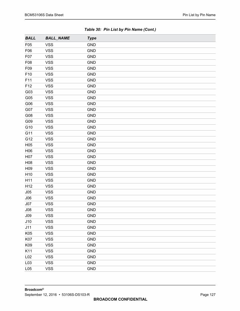
Pin List by Pin NameBCM53106S Data Sheet
BROADCOM CONFIDENTIAL
Broadcom®
September 12, 2016 • 53106S-DS103-R Page 127
F05 VSS GND
F06 VSS GND
F07 VSS GND
F08 VSS GND
F09 VSS GND
F10 VSS GND
F11 VSS GND
F12 VSS GND
G03 VSS GND
G05 VSS GND
G06 VSS GND
G07 VSS GND
G08 VSS GND
G09 VSS GND
G10 VSS GND
G11 VSS GND
G12 VSS GND
H05 VSS GND
H06 VSS GND
H07 VSS GND
H08 VSS GND
H09 VSS GND
H10 VSS GND
H11 VSS GND
H12 VSS GND
J05 VSS GND
J06 VSS GND
J07 VSS GND
J08 VSS GND
J09 VSS GND
J10 VSS GND
J11 VSS GND
K05 VSS GND
K07 VSS GND
K09 VSS GND
K11 VSS GND
L02 VSS GND
L03 VSS GND
L05 VSS GND
Table 30: Pin List by Pin Name (Cont.)
BALL BALL_NAME Type

Pin List by Pin NameBCM53106S Data Sheet
BROADCOM CONFIDENTIAL
Broadcom®
September 12, 2016 • 53106S-DS103-R Page 128
L07 VSS GND
L09 VSS GND
L11 VSS GND
M07 VSS GND
M09 VSS GND
M11 VSS GND
P07 VSS GND
P11 VSS GND
R03 VSS GND
T01 VSS GND
T02 VSS GND
T16 VSS GND
H01 WAN_RXCLK –
H02 WAN_RXD_0 –
J01 WAN_RXD1 –
K01 WAN_RXD2 No connect
K02 WAN_RXD3 No connect
J02 WAN_RXDV –
G01 WAN_TXCLK –
E02 WAN_TXD0 –
E03 WAN_TXD1 –
F01 WAN_TXD2 –
F02 WAN_TXD3 –
F03 WAN_TXEN –
K03 WAN_VDDP –
G02 WAN_VOL_REF –
T03 XTAL_N –
T04 XTAL_P –
R04 XTAL_VDD Power
Table 30: Pin List by Pin Name (Cont.)
BALL BALL_NAME Type
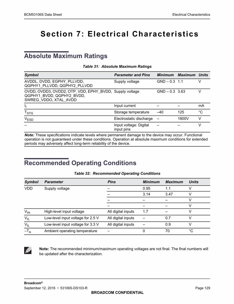
Electrical CharacteristicsBCM53106S Data Sheet
BROADCOM CONFIDENTIAL
Broadcom®
September 12, 2016 • 53106S-DS103-R Page 129
Section 7: Electrical Characteristics
Absolute Maximum Ratings
Recommended Operating Conditions
Table 31: Absolute Maximum Ratings
Symbol Parameter and Pins Minimum Maximum Units
AVDDL, DVDD, EGPHY_PLLVDD,QGPHY1_PLLVDD, QGPHY2_PLLVDD
Supply voltage GND – 0.3 1.1 V
OVDD, OVDD3, OVDD2, OTP_VDD, EPHY_BVDD,QGPHY1_BVDD, QGPHY2_BVDD,SWREG_VDDO, XTAL_AVDD
Supply voltage GND – 0.3 3.63 V
II Input current – – mA
TSTG Storage temperature –40 125 °C
VESD Electrostatic discharge – 1800V V
– Input voltage: Digitalinput pins
– – V
Note: These specifications indicate levels where permanent damage to the device may occur. Functionaloperation is not guaranteed under these conditions. Operation at absolute maximum conditions for extendedperiods may adversely affect long-term reliability of the device.
Table 32: Recommended Operating Conditions
Symbol Parameter Pins Minimum Maximum Units
VDD Supply voltage – 0.95 1.1 V
– 3.14 3.47 V
– – – V
– – – V
VIH High-level input voltage All digital inputs 1.7 – V
VIL Low-level input voltage for 2.5 V All digital inputs – 0.7 V
VIL Low-level input voltage for 3.3 V All digital inputs – 0.9 V
–TA Ambient operating temperature – 0 70 °C
Note: The recommended minimum/maximum operating voltages are not final. The final numbers willbe updated after the characterization.

Electrical CharacteristicsBCM53106S Data Sheet
BROADCOM CONFIDENTIAL
Broadcom®
September 12, 2016 • 53106S-DS103-R Page 130
Electrical Characteristics
Table 33: Electrical Characteristics
Symbol Parameter Pins Conditions Min. Typical Max. Units
IDD Supply current(for 2x RGMIIoperation)
1.0V power rail (analog) Measured – 75.65 – mA
1.0V power rail (digital) Measured – 131 – mA
3.3V power rail (excludingOVDD and OVDD3)
Measured – 95.5 – mA
OVDD_IMP and OVDD_WAN(2.5V for RGMII)
Measured – 18 – mA
VOH High-leveloutput voltage
Digital output pins at 3.3V Ioh = –8 mA 2.4 – – V
Digital output pins at 3.3V IOH = –8 mA 2.0 – – V
Digital output pins at 1.5V IOH = –8 mA 1.0 – – V
VOL Low-leveloutput voltage
Digital output pins at 3.3V IOL = 8 mA – – 0.4 V
Digital output pins at 2.5V IOL= 8 mA – – 0.4 V
Digital output pins at 1.5V IOL = 8 mA – – 0.4 V
VIH High-level inputvoltage
Digital input pins at 3.3V and2.5V
– 1.7 – – V
Digital input pins at 1.5V – 0.9 – – V
XTALI – 1.7 – – V
VIL Low-level inputvoltage
Digital input pins for 3.3V – – – 0.9 V
Digital input pins for 2.5V – – – 0.7 V
Digital input pins at 1.5V – – – 0.5 V
XTALI – – – 0.8 V
II Input current Digital Inputs w/pull-upresistors
– – – – µA
Digital Inputs w/pull-upresistors
– – – – µA
Digital Inputs w/pull-downresistors
– – – – µA
Digital Inputs w/pull-downresistors
– – – – µA
All other digital inputs – – – – µA
Note:The measured result is based on 3.3V PHY and 120 m cable length. The 3m result will be similar.The measured result of 2.5V PHY power rail will be 65 µA lower than 3.3V PHY.The measured condition of RGMII interface is 100 Mbps.

Electrical CharacteristicsBCM53106S Data Sheet
BROADCOM CONFIDENTIAL
Broadcom®
September 12, 2016 • 53106S-DS103-R Page 131
Table 34: Internal Voltage Regulator Electrical Characteristics
Parameter Min Typ Max
Switching Frequency – TBD –
1.8V Regulator Output Range TBD – TBD
1.8V Regulator Output Ripple – TBD –
1.8V Output Current – – TBD
1.8V Ramp Up Time – – TBD
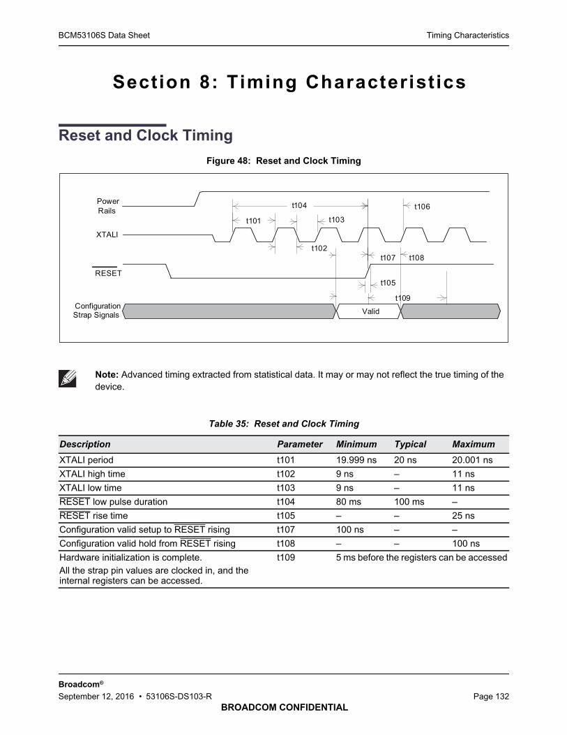
Timing CharacteristicsBCM53106S Data Sheet
BROADCOM CONFIDENTIAL
Broadcom®
September 12, 2016 • 53106S-DS103-R Page 132
Section 8: Timing Characteristics
Reset and Clock Timing
Figure 48: Reset and Clock Timing
Note: Advanced timing extracted from statistical data. It may or may not reflect the true timing of thedevice.
Table 35: Reset and Clock Timing
Description Parameter Minimum Typical Maximum
XTALI period t101 19.999 ns 20 ns 20.001 ns
XTALI high time t102 9 ns – 11 ns
XTALI low time t103 9 ns – 11 ns
RESET low pulse duration t104 80 ms 100 ms –
RESET rise time t105 – – 25 ns
Configuration valid setup to RESET rising t107 100 ns – –
Configuration valid hold from RESET rising t108 – – 100 ns
Hardware initialization is complete.All the strap pin values are clocked in, and theinternal registers can be accessed.
t109 5 ms before the registers can be accessed
Power
Rails
XTALI
RESET
ConfigurationStrap Signals Valid
t104
t101 t103
t106
t102
t107 t108
t105
t109

RGMII Interface TimingBCM53106S Data Sheet
BROADCOM CONFIDENTIAL
Broadcom®
September 12, 2016 • 53106S-DS103-R Page 133
RGMII Interface Timing
The following specifies timing information regarding the IMP interface pins when configured in RGMII mode.
RGMII Output Timing (Normal Mode)
Figure 49: RGMII Output Timing (Normal Mode)
Note: Advanced timing extracted from statistical data. It may or may not reflect the true timing of thedevice.
Table 36: RGMII Output Timing (Normal Mode)
Description Parameter Minimum Typical Maximum Unit
MII1_TXC clock period (1000Mmode)
– 7.2 8 8.8 ns
MII1_TXC clock period (100Mmode)
– 36 40 44 ns
MII1_TXC clock period (10M mode) – 360 400 440 ns
TskewT: Data to clock output skew t201 –500 (1000M) 0 +500 (1000M) ps
TskewT: Data to Clock at 1.5V mode t201 –750 (1000M) 0 +500 (1000M) ps
Duty cycle for 1000M (GbE) – 45 50 55 %
Duty cycle for 10/100M (FE) – 40 50 60 %
Note: The output timing in 10/100M operation is always as specified in the delayed mode.
GTX_CLK(at source)
TX_CTL
t201
TXD[3:0]
t201

RGMII Interface TimingBCM53106S Data Sheet
BROADCOM CONFIDENTIAL
Broadcom®
September 12, 2016 • 53106S-DS103-R Page 134
RGMII Output Timing (Delayed Mode)
Figure 50: RGMII Output Timing (Delayed Mode)
Note: Advanced timing extracted from statistical data. It may or may not reflect the true timing of thedevice.
Table 37: RGMII Output Timing (Delayed Mode)
Description Parameter Minimum Typical Maximum Unit
MII1_TXC clock period (1000M mode) – 7.2 8 8.8 ns
MII1_TXC clock period (100M mode) – 36 40 44 ns
MII1_TXC clock period (10M mode) – 360 400 440 ns
TsetupTData valid to clock transition:Available setup time at the outputsource (delayed mode)
t201D 1.2(all speeds)
2.0 – ns
TholdTClock transition to data valid:Available hold time at the outputsource (delayed mode)
t202D 1.2(all speeds)
2.0 – ns
TsetupTData valid to clock transition:Available setup time at the outputsource (1.5V mode)
t201D 1.0(all speeds)
2.0 – ns
TholdTClock transition to data valid:Available hold time at the outputsource (1.5V mode)
t202D 1.0(all speeds)
2.0 – ns
Duty cycle for 1000M (GbE) – 45 50 55 %
Duty cycle for 10/100M (FE) – 40 50 60 %
Delayed
GTX_CLK(actual output
at source)
TX_CTRL
t201D
TXD[3:0]
t201D
t202D
t202D
GTX_CLK(internal)

RGMII Interface TimingBCM53106S Data Sheet
BROADCOM CONFIDENTIAL
Broadcom®
September 12, 2016 • 53106S-DS103-R Page 135
RGMII Input Timing (Normal Mode)
Figure 51: RGMII Input Timing (Normal Mode)
Note: Advanced timing extracted from statistical data. It may or may not reflect the true timing of thedevice.
Table 38: RGMII Input Timing (Normal Mode)
Description Parameter Minimum Typical Maximum Unit
MII1_RXC clock period (1000M mode) – 7.2 8 8.8 ns
MII1_RXC clock period (100M mode) – 36 40 44 ns
MII1_RXC clock period (10M mode) – 360 400 440 ns
TsetupRInput setup time: Valid data to clock
t301 1.0 2.0 – ns
TholdRInput hold time: Clock to valid data
t302 1.0 2.0 – ns
Duty cycle for 1000M (GbE) – 45 50 55 %
Duty cycle for 10/100M (FE) – 40 50 60 %
RXCLK(internal)
RX_CTRLRXD[3:0]
RXCLK(actual )
t302 t301
t302t301

RGMII Interface TimingBCM53106S Data Sheet
BROADCOM CONFIDENTIAL
Broadcom®
September 12, 2016 • 53106S-DS103-R Page 136
RGMII Input Timing (Delayed Mode)
Figure 52: RGMII Input Timing (Delayed Mode)
Note: Advanced timing extracted from statistical data. It may or may not reflect the true timing of thedevice.
Table 39: RGMII Input Timing (Delayed Mode)
Description Parameter Minimum Typical Maximum Unit
TsetupRInput setup time (delayed mode)
t301D –1.0 (1000M) – – ns
–1.0 (10/100M) – – ns
TholdRInput hold time (delayed mode)
t302D 3.0 (1000M) – – ns
9.0 (10/100M) – – ns
RXCLK( internal)
RX_CTRLRXD[3:0]
Delayed RXCLK(Actual output at
destination)
t301Dt301Dt302D t302D

MDC/MDIO TimingBCM53106S Data Sheet
BROADCOM CONFIDENTIAL
Broadcom®
September 12, 2016 • 53106S-DS103-R Page 137
MDC/MDIO Timing
The following specifies timing information regarding the MDC/MDIO interface pins.
Figure 53: MDC/MDIO Timing (Slave Mode)
Note: Advanced timing extracted from statistical data. It may or may not reflect the true timing of thedevice.
Table 40: MDC/MDIO Timing (Slave Mode)
Description Parameter Minimum Typical Maximum Unit
MDC cycle time t401 80 – – ns
MDC high/low – 30 – – ns
MDC rise/fall time t402 – – 10 ns
MDIO input setup time to MDC rising t403 7.5 – – ns
MDIO input hold time from MDC rising t404 7.5 – – ns
MDIO output delay from MDC rising t405 0 – 45 ns
MDIO
(Input)
MDC
MDIO
(Output)
t405
t403
t401
t404
t402
t402

MDC/MDIO TimingBCM53106S Data Sheet
BROADCOM CONFIDENTIAL
Broadcom®
September 12, 2016 • 53106S-DS103-R Page 138
Figure 54: MDC/MDIO Timing (Master Mode)
Table 41: MDC/MDIO Timing (Master Mode)
Description Parameter Minimum Typical Maximum Unit
MDC cycle time t401 400 – – ns
MDC high/low – 160 – 240 ns
MDC rise/fall time t402 – – 10 ns
MDIO input setup time to MDC rising t403 20 – – ns
MDIO input hold time from MDC rising t404 7.5 – – ns
MDIO output delay from MDC falling t405m –5 – 20 ns
MDIO
(Into PHY)
MDC
MDIO
(From PHY)
t405m
t403
t401
t404
t402
t402

Serial LED Interface TimingBCM53106S Data Sheet
BROADCOM CONFIDENTIAL
Broadcom®
September 12, 2016 • 53106S-DS103-R Page 139
Serial LED Interface Timing
The following specifies timing information regarding the LED interface pins.
Figure 55: Serial LED Interface Timing
Note: Advanced timing extracted from statistical data. It may or may not reflect the true timing of thedevice.
Table 42: Serial LED Interface Timing
Description Parameter Minimum Typical Maximum Unit
LED update cycle period t301 – 42 – ms
LEDCLK period t302 – 320 – ns
LEDCLK high-pulse width t303 150 – 170 ns
LEDCLK low-pulse width t304 150 – 170 ns
LEDCLK to LEDDATA output time t305 140 – 180 ns
LEDDATA
LEDCLK
t301
S0 S1 S2 S S0N
t305
t302
t303
t304
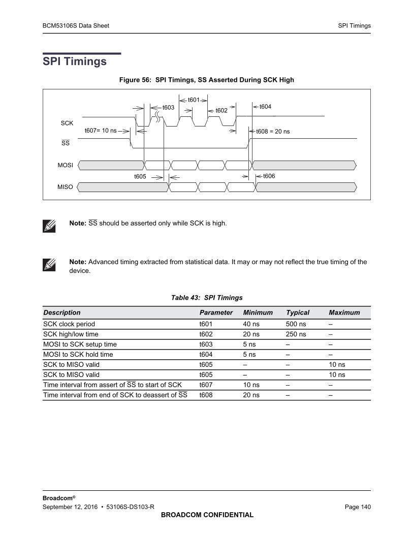
SPI TimingsBCM53106S Data Sheet
BROADCOM CONFIDENTIAL
Broadcom®
September 12, 2016 • 53106S-DS103-R Page 140
SPI Timings
Figure 56: SPI Timings, SS Asserted During SCK High
Note: SS should be asserted only while SCK is high.
Note: Advanced timing extracted from statistical data. It may or may not reflect the true timing of thedevice.
Table 43: SPI Timings
Description Parameter Minimum Typical Maximum
SCK clock period t601 40 ns 500 ns –
SCK high/low time t602 20 ns 250 ns –
MOSI to SCK setup time t603 5 ns – –
MOSI to SCK hold time t604 5 ns – –
SCK to MISO valid t605 – – 10 ns
SCK to MISO valid t605 – – 10 ns
Time interval from assert of SS to start of SCK t607 10 ns – –
Time interval from end of SCK to deassert of SS t608 20 ns – –
SCK
SS
MOSI
MISO
t601
t602t603 t604
t605 t606
t608 = 20 nst607= 10 ns

EEPROM TimingBCM53106S Data Sheet
BROADCOM CONFIDENTIAL
Broadcom®
September 12, 2016 • 53106S-DS103-R Page 141
EEPROM Timing
Figure 57: EEPROM Timing
Note: Advanced timing extracted from statistical data. It may or may not reflect the true timing of thedevice.
Table 44: EEPROM Timing
Description Parameter Minimum Typical Maximum
SCK clock frequency t701 – 100 kHz –
SCK high/low time t702 – 5 µs –
SCK low to CS, DI valid t703 – – 500 ns
SCK low to CS, DI invalid t704 500 ns – –
DO to SCK falling setup time t705 200 ns – –
DO to SCK falling hold time t706 200 ns – –
SCK
CS
DI
DO
t701
t702t703 t704
t705 t706

Thermal CharacteristicsBCM53106S Data Sheet
BROADCOM CONFIDENTIAL
Broadcom®
September 12, 2016 • 53106S-DS103-R Page 142
Section 9: Thermal Characteristics
Package Only
Package Only with Heat Sink (50 x 50 x 35 mm)
Table 45: Package only, 2s2p PCB, TA = 70° C, P = 1.723W
Device power dissipation, P (W) 1.72
Ambient air temperature TA (°C) 70
JA in still air (°C/W) 38.17
JB (°C/W) 17.32
JB (°C/W) 23.74
2s2p board, pkg only
Package Thermal Performance Curve
Air Velocity TJ
(°C)
TT
(°C)JA
(°C/W)JT
(°C/W)JB
(°C/W)m/s ft/min
0 0 135.8 133.5 38.17 1.30 25.74
0.508 100 132.4 130.1 36.19 1.32 25.77
1.016 200 130.7 128.3 35.21 1.38 25.74
2.032 400 128.8 126.1 34.11 1.55 25.62
3.048 600 127.6 124.6 33.43 1.71 25.50
Table 46: Package with External Heat Sink 50 x 50 x 35 mm, 2s2p PCB, TA = 70° C, P = 1.723W
Device power dissipation, P (W) 1.72
Ambient air temperature TA (°C) 70
JA in still air (°C/W) 23.75
JB (°C/W) 17.32
JB (°C/W) 23.74
2s2p board, 50 x 50 x 35 mm estHS
Package Thermal Performance Curve
Air Velocity TJ
(°C)
TT
(°C)JA
(°C/W)JT
(°C/W)JB
(°C/W)m/s ft/min
0 0 110.9 82.0 23.75 16.78 17.47
0.508 100 105.9 76.4 20.82 17.10 17.19
1.016 200 104.8 75.3 20.20 17.15 17.15
2.032 400 104.2 74.7 19.87 17.15 17.14
3.048 600 104.2 74.5 19.73 17.14 17.14

Thermal CharacteristicsBCM53106S Data Sheet
BROADCOM CONFIDENTIAL
Broadcom®
September 12, 2016 • 53106S-DS103-R Page 143
Package Only
Package Only with Heat Sink (19 x 19 x 5 mm)
Table 47: Package only, 2s2p PCB, TA = 55 °C, P = 1.723W
Device power dissipation, P (W) 1.72
Ambient air temperature TA (°C) 55
JA in still air (°C/W) 38.65
JB (°C/W) 17.32
JB (°C/W) 23.74
2s2p board, pkg only
Package Thermal Performance Curve
Air Velocity TJ
(°C)
TT
(°C)JA
(°C/W)JT
(°C/W)JB
(°C/W)m/s ft/min
0 0 121.6 119.4 38.65 1.29 25.74
0.508 100 117.8 115.5 36.43 1.31 25.77
1.016 200 116.0 113.6 35.38 1.36 25.75
2.032 400 114.0 111.3 34.23 1.54 25.63
3.048 600 112.8 109.8 33.52 1.70 25.51
Table 48: Package with External Heat Sink 19.x 19 x 5 mm, 2s2p PCB, TA = 55° C, P = 1.723W
Device power dissipation, P (W) 1.72
Ambient air temperature TA (°C) 55
JA in still air (°C/W) 31.70
JB (°C/W) 17.32
JB (°C/W) 23.74
2s2p board, pkg only
Package Thermal Performance Curve
Air Velocity TJ
(°C)
TT
(°C)JA
(°C/W)JT
(°C/W)JB
(°C/W)m/s ft/min
0 0 109.6 84.5 31.70 14.58 19.66
0.508 100 105.3 79.8 29.20 14.82 19.46
1.016 200 102.1 76.0 27.31 15.13 19.17
2.032 400 98.7 72.0 25.34 15.49 18.80
3.048 600 96.9 69.9 24.33 15.68 18.59

Mechanical InformationBCM53106S Data Sheet
BROADCOM CONFIDENTIAL
Broadcom®
September 12, 2016 • 53106S-DS103-R Page 144
Section 10: Mechanical Information
Figure 58: BCM53106S Mechanical Information

Ordering InformationBCM53106S Data Sheet
BROADCOM CONFIDENTIAL
Broadcom®
September 12, 2016 • 53106S-DS103-R Page 145
Section 11: Ordering Information
Table 49: Ordering Information
Part Number Package Ambient Temperature
BCM53106SKFBG 212-pin FBGA package 0°C–70°C
BCM53106SIFBG 212-pin FBGA package –45°C–85°C

Web: www.broadcom.comCorporate Headquarters: San Jose, CA© 2016 by Broadcom. All rights reserved.
53106S-DS103-R September 12, 2016
BCM53106S Data Sheet