multiobjective optimization of ultraflat magnetic … transactions on power electronics, vol. 28,...
TRANSCRIPT

© 2013 IEEE
IEEE Transactions on Power Electronics, Vol. 28, No. 7, pp. 3591-3602, July 2013
Multiobjective Optimization of Ultraflat Magnetic Components With PCB-Integrated Core
C. Marxgut,J. Mühlethaler,F. Krismer,J. W. Kolar
This material is published in order to provide access to research results of the Power Electronic Systems Laboratory / D-ITET / ETH Zurich. Internal or personal use of this material is permitted. However, permission to reprint/republish this material for advertising or promotional purposes or for creating new collective works for resale or redistribution must be obtained from the copyright holder. By choosing to view this document, you agree to all provisions of the copyright laws protecting it.

IEEE TRANSACTIONS ON POWER ELECTRONICS, VOL. 28, NO. 7, JULY 2013 3591
Multiobjective Optimization of Ultraflat MagneticComponents With PCB-Integrated CoreChristoph Marxgut, Student Member, IEEE, Jonas Muhlethaler, Student Member, IEEE,
Florian Krismer, Member, IEEE, and Johann W. Kolar, Fellow, IEEE
Abstract—In future applications, e.g., in ultra-flat OLED lampdrivers or flat screen power supplies, ultra-flat ac/dc and dc/dcconverter systems are highly demanded. Therefore, the designand implementation of a printed circuit board (PCB)-integratedflyback transformer for a 1-mm-thin single-phase power factorcorrection rectifier is under investigation. In this paper, first anoverview on several integration methods is given. It is shown thatthe PCB integration of magnetic cores allows us to achieve the re-quired thickness of 1 mm and a high energy density. In a next step,the design and the realization of ultra-flat magnetic componentswith PCB-integrated cores are discussed in detail. The presentedmulti-objective design procedure determines the inductor and/ortransformer setup optimal with respect to minimal losses and/orminimal footprint area; for this purpose, all required electrical,magnetic, and geometrical parameters of the magnetic componentare considered in the design process. Furthermore, all specific im-plications entailed by the PCB-integrated core, e.g., the core setup,anisotropic core losses, the interleaving of windings, or an accuratereluctance model are treated. Finally, experimental results are usedto verify the design procedure.
Index Terms—Flyback transformer, PCB-integrated trans-former, printed circuit board (PCB)-integrated inductor, powersheet, ultra-flat magnetics.
I. INTRODUCTION
U LTRAFLAT power converters are increasingly needed forspecific future applications, such as, e.g., ultra-flat OLED
lamp drivers [1]–[4] or flat screen power supplies [5]. The re-spective power converters are single-phase power factor correc-tion (PFC) rectifiers, which provide an output power between20 and 200 W at a constant dc voltage (typically 10–20 V); thetotal converter height limit is typically 1–2 cm [6].
The Power Electronic Systems Laboratory at ETH Zurichaims to outperform this height requirement by a factor of 10 andto realize a PFC rectifier with a total height of only 1 mm. Therelated research project, entitled the Power Sheet [7], focuses onthe analysis and the comprehension of the implications of theextremely low converter height on the PFC rectifier’s efficiencyand on the total required footprint area. Furthermore, the optimal
Manuscript received July 11, 2012; revised September 7, 2012 and October15, 2012; accepted October 15, 2012. Date of current version December 24,2012. Recommended for publication by Associate Editor C. R. Sullivan.
The authors are with the Power Electronic Systems Laboratory, SwissFederal Institute of Technology Zurich, 8092 Zurich, Switzerland (e-mail:[email protected]; [email protected]; [email protected]; [email protected]).
Color versions of one or more of the figures in this paper are available onlineat http://ieeexplore.ieee.org.
Digital Object Identifier 10.1109/TPEL.2012.2226917
converter design, with respect to efficiency or footprint area, isinvestigated.
Except for the magnetic components, all active convertercomponents (e.g., power MOSFETs and control ICs) are avail-able either in thin packages with thicknesses of less than 1 mm(i.e., thin SMD packaged semiconductor components) or as barechips. Also, thin ceramic capacitors with thicknesses of less than1 mm are commercially available [8], [9]. Printed circuit boards(PCB) with a total thickness of less than 1 mm can be realizedand the aforementioned components (semiconductors, capaci-tors, and control circuits) can be embedded into the PCB [10].Thus, the implementation of ultra-flat magnetic components isthe main challenge that needs to be solved to keep the 1 mmheight limit.
For realizing inductive components in an initial step, powerSMD inductors could be considered; however, the total heightof the flattest available power SMD inductors is over 3 mm [11].As an alternative, planar magnetic cores and a multilayer PCBcould be used to realize ultra-flat magnetic components [12].Still, the realization of the required ultra-flat magnetic compo-nents is unfeasible, since the minimal total height of availableplanar cores is 5 mm (e.g., ELP 14/3.5/5 by [13]). In a differ-ent approach, flat magnetic components are implemented withPCB inductors consisting of spiral windings on several layers,which are covered with magnetic material [14]. Based on thisintegration method, a transformer for a 60 W power converter isrealized in [15] (PCB thickness: 4 mm). The implemented coreemploys a ferrite polymer compound with a low relative per-meability (typically μr = 10 . . . 20 ); therefore, a considerablylarge area is required in order to obtain the desired inductancevalue. Accordingly, this technique facilitates the realization ofthin inductors; however, the energy density of the inductors islow due to the inherently large air gap length.
A reduced air gap length and an increased energy density areachieved if the core of the magnetic component is integrated intothe PCB. In [16], the PCB integration of highly permeable mag-netic materials (Ni80Fe20) is discussed; PCB-integrated corestructures with a thickness of 1.3 mm have been built and areused as inductors for a 1.5 W buck converter. A comparisonbetween closed core structures and air inductors is given, andit is shown that closed core assemblies provide the highest in-ductance and efficiency values per area. Since the employedmagnetic cores are very thin (10–20 μm), a large area is re-quired to avoid saturation for a given current and to achieve arequired inductance value. Furthermore, in [16], the eddy cur-rent losses in the magnetic cores are large due to the selectedarrangement of the winding and the core.
0885-8993/$31.00 © 2012 IEEE

3592 IEEE TRANSACTIONS ON POWER ELECTRONICS, VOL. 28, NO. 7, JULY 2013
Fig. 1. PCB-integrated core; windings are realized with PCB tracks and vias.
TABLE ISPECIFICATIONS OF THE Power Sheet AT A THICKNESS OF 1 mm
O’Mathuna et al. [17] present a comprehensive review of in-tegrated magnetics and describe several integration methods forinductors. However, the discussion focuses on very high fre-quency (HF) (1–100 MHz) point-of-load buck converters, e.g.,for mobile phones, or multicore processors, with high currentand low voltage capability. For an ac/dc rectifier where the isola-tion between the windings is crucial and the switching frequencyis typically limited below 1 MHz, these integrated inductors arenot feasible.
In [18], a ferrite core (Ferroxcube 3F3 [19]) is integratedinto a PCB and applied to a buck converter (3.3 V/20 A). Theinductance value is 1 μH and the integrated core has a thick-ness of 2 mm. Ferrite materials feature low core losses but it isvery brittle and as the required magnetic cores are extremely thin(< 1 mm), the production of ferrite cores is very difficult. There-fore, ferrites are not considered as an appropriate choice. Thus,amorphous and nanocrystalline soft magnetic materials remain,which enable a simpler manufacturing of ultrathin cores com-pared to ferrite cores. Zhang and Sanders [20] present a PCB-integrated transformer for a 200 W dc/dc converter employingan amorphous core material. Fig. 1 illustrates the constructionof the magnetic component. However, the modeling of the trans-former only accounts for eddy current losses and the geometryis restricted to toroidal cores.
This paper investigates the applicability of nanocrystallineand amorphous soft magnetic materials for the realization ofultra-flat magnetic components with almost arbitrary shape. Thisis illustrated on the example of the HF transformer of a single-phase flyback-type PFC rectifier with a total converter height of1 mm and specifications according to Table I. The considered200 W PFC rectifier, as presented in Fig. 2, is composed of sixparallel flyback modules. The discussion in this paper refers toone of these six Power Sheets each rated with an output powerof Pout,mod = 33 W. The rectifier operates with zero-voltageswitching, close to the boundary between continuous conduc-tion mode and discontinuous conduction mode, to achieve lowswitching losses [21]. The system features only a single mag-netic power component, i.e., the flyback transformer. A more
Fig. 2. Flyback-type single-phase PFC rectifier system, specified in Table I.The system is split up into six parallel interleaved modules (Nm od = 6) inorder to reduce the input and output capacitor currents. Each one of the parallelmodules is referred as a Power Sheet.
common approach with input-side boost-type PFC rectifier andseries-connected dc–dc converter shows a larger footprint areathan the flyback-type approach, due to the two required magneticcomponents, i.e., the boost inductor and the HF transformer ofthe dc–dc converter.
The design of a PCB-integrated core differs from the designof conventionally shaped cores. Therefore, Section II discussesthe specific requirements that need to be considered in the de-sign, and Section III subsequently presents the optimization ofultra-flat magnetic components with respect to minimum to-tal footprint area and/or minimum losses. The results of themulti-objective optimization are presented as η-α-Pareto Front,which shows the tradeoff between the area-related power den-sity α (W/cm2) and the efficiency η for a given magnetic corematerial.
Section IV presents measurement results obtained from aselected flyback transformer design being used in a dc–dc con-verter and in a single-phase PFC rectifier that are used to verifythe theoretical considerations.
II. DESIGN CONSIDERATIONS FOR ULTRA-FLAT
MAGNETIC COMPONENTS
The PCB integration of the core implies several specific prop-erties and restrictions on the design of an inductor or trans-former. This section discusses these implications required for themulti-objective design procedure presented in Section III and isdivided into the following sections.Section II-A summarizes the properties of the considered mag-
netic materials and discusses possible core constructions.Section II-B emphasizes the importance of the isolation between
the core tapes as otherwise the core losses increase vastly.Section II-C focuses on the anisotropy of nanocrystalline and
amorphous materials which results in increased losses in theeasy magnetization direction.
Section II-D proposes a limit of the power loss per area in orderto restrict the core temperature.
Section II-E presents an accurate reluctance model re-quired for the inductance calculation of specific coregeometries.
Section II-F details an interleaved winding arrangement fortransformer applications.
A. Core Geometry and Materials
In order to integrate an inductor or a transformer into a PCB,the setup of the core has to be taken into consideration. There are

MARXGUT et al.: MULTIOBJECTIVE OPTIMIZATION OF ULTRAFLAT MAGNETIC COMPONENTS WITH PCB-INTEGRATED CORE 3593
Fig. 3. Core configurations applicable to PCB-integrated transformers and in-ductors. (a) Two C-shaped core halves with stacked magnetic foils. (b) Toroidalcore with a wound magnetic foil. In the latter setup (b), an air gap can only beinserted with considerable effort after embedding the core into the PCB.
Fig. 4. (a) Magnetic sheets are cut out of a long band of magnetic foil.(b) Square inductor with a magnetic core formed by stacking ten sheets(VC6155F by VAC [23]) is shown. (c) Temperature rise in the easy direc-tion is much higher compared to the hard direction (fS = 100 kHz, ΔB =1.5 T, Ploss = 2.2 W).
basically two possible constructions for PCB-integrated mag-netics employing nanocrystalline and amorphous materials. Thecore can either be composed of a stack of thin magnetic foils[cf., Fig. 3(a)] or it consists of a thin toroidally wound mag-netic foil [cf., Fig. 3(b)]. However, an air gap, which offers thedesigner an additional degree of freedom, can only be easily re-alized for stacked assemblies as toroidally wound cores wouldfall apart. Only with a sophisticated core attachment inside thePCB an air gap can be implemented. The integration of the coreinto the PCB requires additional manufacturing effort comparedto standard PCB production. However, this technology is alreadyavailable (see, e.g., [22]) and thus not in the scope of this paper.
As mentioned Section I, nanocrystalline and amorphous ma-terials are beneficial as ultrathin tapes of these materials areavailable that are suitable to realize the geometries in Fig. 3.These tapes feature a thickness of 20 μm or less and are appli-cable to HF applications. However, the width of the tapes, a,(cf., Fig. 4) is limited due to manufacturing reasons. This is alimitation in the design process of an integrated inductor andcauses the cores to be either composed of several core legs orof a monolithic core with rather rectangular (cf., Fig. 5) thanquadratic shape [cf., Fig. 4(b)] as otherwise the winding win-dow [cf., Fig. 4(a)] would be too small to provide space for thewindings.
Fig. 5. Core geometry for the flux density calculation. To calculate the fluxdensity and to determine the Steinmetz parameters for the easy direction, arectangular-shaped core without air gap is considered.
Nanocrystalline materials are typically annealed in order tofeature the specified magnetic properties. However, after the an-nealing process, these materials are very brittle, which makes afurther mechanical treatment impossible. On the contrary, amor-phous materials remain processable after being annealed. Amor-phous materials are thus considered in this paper as they arebeneficial for prototyping, whereas nanocrystalline cores needto be produced by the material manufacturer.
In this paper, the materials VITROVAC6155F by [23], termedin the following as VC6155F, and 2714A by [24] are in-vestigated. Both materials are Cobald-based alloys, whereasVC6155F is field-annealed contrary to 2714A which is no-field annealed. Amorphous cores are typically employed forHF transformer and inductor applications and are available byvarious manufacturers [23]–[27].
B. Core Lamination
Lamination of magnetic cores is widely used for HF trans-formers and inductors as eddy currents and thus eddy currentinduced losses in the core material can be reduced. Therefore,the isolation between the magnetic foils is crucial to achieve lowcore losses in HF applications. Amorphous materials feature aninherent oxidation layer which reduces the conductance betweentwo foils. However, measurement results show that the isolationprovided by the oxide layer is insufficient. Two prototypes havebeen built up, where in the first one the magnetic foils are looselyembedded into the PCB, and in the second one, the core is tightlypressed into the PCB. It turns out that the losses increase withincreasing pressure on the stack of foils (which increases theconductivity between the magnetic foils). The measurementshave shown that the pressed setup generates three times higherlosses than the loose realization (ΔB = 0.4 T, fS = 100 kHz:Ploose = 8.9 W, Ptight = 29.25 W).
To increase the resistance between the magnetic foils, ei-ther isolation tapes or isolation lacquer has to be employed.The addition of the isolation decreases the core fill factor kfethat defines the ratio between the magnetically effective corecross-sectional area to the total cross section of the core. Thishas to be considered in the design procedure. Throughout thispaper, the core foils are isolated using an isolation laquer in

3594 IEEE TRANSACTIONS ON POWER ELECTRONICS, VOL. 28, NO. 7, JULY 2013
order to obtain minimal core losses while keeping the core fillfactor high.
C. Core Losses
An alternating magnetic flux in the core results in eddy currentlosses and hysteresis losses. A comparison between stacked andwound cores [cf., Fig. 3], however, shows that equal eddy currentlosses result for both configurations [28].
Hysteresis losses, however, show different behavior for bothcore configurations as nanocrystalline and amorphous materialsare generally anisotropic, and there is an easy and a hard mag-netizing direction of the foils. In toroidally wound cores, theflux is always in the tangential and therefore hard direction [cf.,Fig. 4(a)]. In magnetic cores consisting of a stack of magneticfoils, the flux is forced to penetrate into the easy magnetizingdirection as well. Fig. 4(a) shows that each sheet of the core iscut out of the magnetic band and the winding window is con-sidered in the middle. The magnetic flux φ flows as indicated inFig. 4(a) and higher losses in the easy magnetization directionhave to be expected.
Fig. 4(b) shows a square prototype inductor which consistsof a stack of ten VC6155F foils (each 20 μm thick) with a sidelength of 35 mm. Fig. 4(c) illustrates that an HF magnetic fluxapplied to the core results in different core losses for each direc-tion; the temperature in the easy direction is higher comparedto the hard direction.
It is, therefore, crucial that the increased losses in the easydirection are considered in the design of a PCB-integrated core.Otherwise, the core could be thermally damaged. Since core lossdata for the hard direction are generally provided by manufac-turers these parameters (kh , αh , and βh ) can easily be extracted.Thus, in order to be able to estimate the total core losses, theSteinmetz parameters for the easy direction remain to be deter-mined. For it, a segmentation of the core according to Fig. 5 isassumed. The flux density in the core, B(x), will decrease pro-portional to the inverse of the magnetic length lm (x) whereasthe maximum flux density Bmax is at the inner border of thecore (xi or yi).
Referring to Ampere’s law and considering Fig. 5, the ratioof the flux density at the outer and the inner edge is
B(x = xi)B(x = xo)
=lm (x = xo)lm (x = xi)
=4 · (xo + yo)4 · (xi + yi)
. (1)
With
lm (x) = 4 · (x + yi + (x − xi) · tan ϕ)
= 4 ·(
x + yi + (x − xi) ·yo − yi
xo − xi
)
the flux density at an arbitrary position x can be determined andis thus
B(x) = Bmax · xi + yi
x + yi + (x − xi) · yo −yi
xo −xi
. (2)
The core losses can be calculated with the Steinmetz equationthat has to be integrated over either an easy or a hard directionsegment. For the two segments in easy direction, the core losses
Fig. 6. (a) Picture and (b) circuit of the used core loss measurement system.
TABLE IIESTIMATION OF THE LOSSES IN EASY MAGNETIZING DIRECTION BASED
ON CORE LOSS MEASUREMENTS AND CALCULATIONS FOR
THE CORE DEPICTED IN FIG. 4(b)
are thus
Pv =2 dcorekfe
∫ xo
xi
∫ yi +(x−xi ) tan ϕ
−yi −(x−xi ) tan ϕ
ke · fαe
S
(ΔB(x)
2
)βe
dydx
(3)with the core thickness dcore and the core filling factor kfe .Equations similar to (2) and (3) can be determined for the hardmagnetizing direction (i.e., ΔB(y)) in the same way.
With this analytical background, the Steinmetz parametersrelated to the easy direction can be extracted from measurementresults. For it, the core losses Pcore of a given core under test(CUT) are measured at a certain operating point (ΔB, fS ) usingthe core loss measurement system shown in Fig. 6 [29]. The corelosses are obtained by applying an HF current to the core and bymeasuring the induced voltage on an auxiliary winding. The timeintegral of the induced voltage is proportional to the magneticflux density in the core, and the applied current is proportionalto the magnetic field. Thus, the core losses are extracted fromthe obtained hysteresis curve.
The core losses in hard direction, Phard , can be calculated byapplying the known Steinmetz parameters and the geometry ofthe CUT to (3). The difference between Pcore and Phard are thelosses in the easy direction parts
Peasy = Pcore − Phard . (4)
Table II presents the calculated and measured core losses for theCUT depicted in Fig. 4(b). In order to increase the accuracy ofthe Steinmetz parameter extraction, several square CUTs havebeen measured with different values of ΔB (0.2 T . . . 1.8 T)and fS (50 kHz . . . 200 kHz). The obtained parameter sets(Peasy ,ΔB, fS , and core geometry) are then applied to (3)which gives a set of equations. Finally, this overdeterminedset of equations is solved for the Steinmetz parameters (ke, αe ,and βe ) using a least-squares algorithm.
Fig. 7 presents a comparison between the amorphous ma-terials VC6155F [23] and 2714A [24] based on the extractedSteinmetz parameters listed in Table III. It is shown thatVC6155F has very low losses in the hard direction but high
MARXGUT et al.: MULTIOBJECTIVE OPTIMIZATION OF ULTRAFLAT MAGNETIC COMPONENTS WITH PCB-INTEGRATED CORE 3595
Fig. 7. Comparison of core losses between VC6155F according to [23] and2714A according to [24] at fS = 100 kHz. VC6155F features low core lossesin the hard direction, whereas 2714A is better regarding the losses in the easydirection.
TABLE IIIPARAMETERS OF MAGNETIC MATERIALS FOR INTEGRATED CORES
losses in the easy direction. 2714A exhibits a more isotropicbehavior.
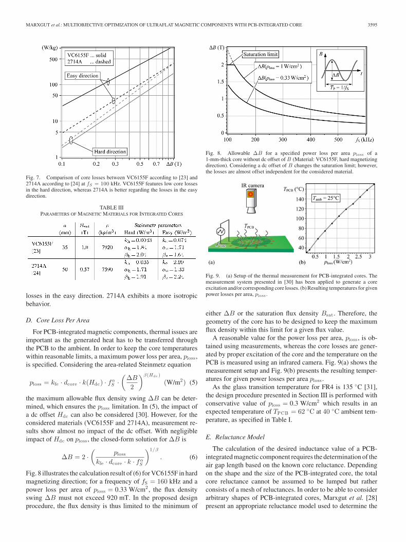
D. Core Loss Per Area
For PCB-integrated magnetic components, thermal issues areimportant as the generated heat has to be transferred throughthe PCB to the ambient. In order to keep the core temperatureswithin reasonable limits, a maximum power loss per area, ploss ,is specified. Considering the area-related Steinmetz equation
ploss = kfe · dcore · k(Hdc) · fαS ·
(ΔB
2
)β (Hd c )
(W/m2) (5)
the maximum allowable flux density swing ΔB can be deter-mined, which ensures the ploss limitation. In (5), the impact ofa dc offset Hdc can also be considered [30]. However, for theconsidered materials (VC6155F and 2714A), measurement re-sults show almost no impact of the dc offset. With negligibleimpact of Hdc on ploss , the closed-form solution for ΔB is
ΔB = 2 ·(
ploss
kfe · dcore · k · fαS
)1/β
. (6)
Fig. 8 illustrates the calculation result of (6) for VC6155F in hardmagnetizing direction; for a frequency of fS = 160 kHz and apower loss per area of ploss = 0.33 W/cm2 , the flux densityswing ΔB must not exceed 920 mT. In the proposed designprocedure, the flux density is thus limited to the minimum of
Fig. 8. Allowable ΔB for a specified power loss per area ploss of a1-mm-thick core without dc offset of B (Material: VC6155F, hard magnetizingdirection). Considering a dc offset of B changes the saturation limit; however,the losses are almost offset independent for the considered material.
Fig. 9. (a) Setup of the thermal measurement for PCB-integrated cores. Themeasurement system presented in [30] has been applied to generate a coreexcitation and/or corresponding core losses. (b) Resulting temperatures for givenpower losses per area, ploss .
either ΔB or the saturation flux density Bsat . Therefore, thegeometry of the core has to be designed to keep the maximumflux density within this limit for a given flux value.
A reasonable value for the power loss per area, ploss , is ob-tained using measurements, whereas the core losses are gener-ated by proper excitation of the core and the temperature on thePCB is measured using an infrared camera. Fig. 9(a) shows themeasurement setup and Fig. 9(b) presents the resulting temper-atures for given power losses per area ploss .
As the glass transition temperature for FR4 is 135 ◦C [31],the design procedure presented in Section III is performed withconservative value of ploss = 0.3 W/cm2 which results in anexpected temperature of TPCB = 62 ◦C at 40 ◦C ambient tem-perature, as specified in Table I.
E. Reluctance Model
The calculation of the desired inductance value of a PCB-integrated magnetic component requires the determination of theair gap length based on the known core reluctance. Dependingon the shape and the size of the PCB-integrated core, the totalcore reluctance cannot be assumed to be lumped but ratherconsists of a mesh of reluctances. In order to be able to considerarbitrary shapes of PCB-integrated cores, Marxgut et al. [28]present an appropriate reluctance model used to determine the
3596 IEEE TRANSACTIONS ON POWER ELECTRONICS, VOL. 28, NO. 7, JULY 2013
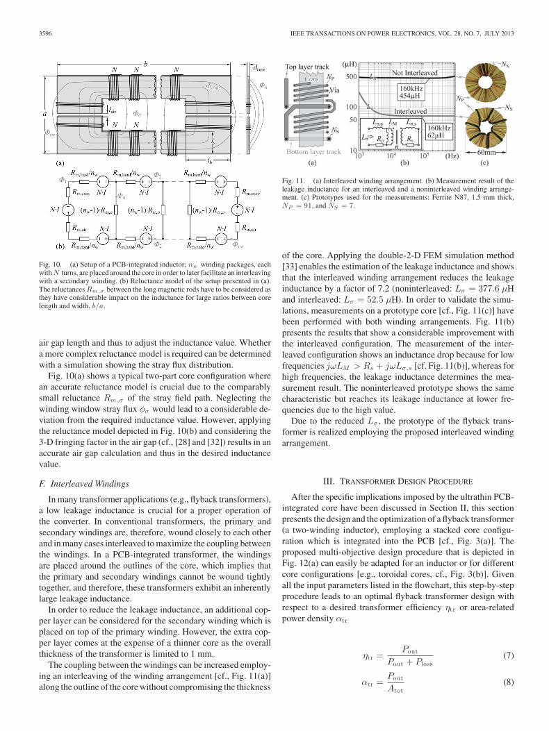
Fig. 10. (a) Setup of a PCB-integrated inductor; nw winding packages, eachwith N turns, are placed around the core in order to later facilitate an interleavingwith a secondary winding. (b) Reluctance model of the setup presented in (a).The reluctances Rm ,σ between the long magnetic rods have to be considered asthey have considerable impact on the inductance for large ratios between corelength and width, b/a.
air gap length and thus to adjust the inductance value. Whethera more complex reluctance model is required can be determinedwith a simulation showing the stray flux distribution.
Fig. 10(a) shows a typical two-part core configuration wherean accurate reluctance model is crucial due to the comparablysmall reluctance Rm,σ of the stray field path. Neglecting thewinding window stray flux φσ would lead to a considerable de-viation from the required inductance value. However, applyingthe reluctance model depicted in Fig. 10(b) and considering the3-D fringing factor in the air gap (cf., [28] and [32]) results in anaccurate air gap calculation and thus in the desired inductancevalue.
F. Interleaved Windings
In many transformer applications (e.g., flyback transformers),a low leakage inductance is crucial for a proper operation ofthe converter. In conventional transformers, the primary andsecondary windings are, therefore, wound closely to each otherand in many cases interleaved to maximize the coupling betweenthe windings. In a PCB-integrated transformer, the windingsare placed around the outlines of the core, which implies thatthe primary and secondary windings cannot be wound tightlytogether, and therefore, these transformers exhibit an inherentlylarge leakage inductance.
In order to reduce the leakage inductance, an additional cop-per layer can be considered for the secondary winding which isplaced on top of the primary winding. However, the extra cop-per layer comes at the expense of a thinner core as the overallthickness of the transformer is limited to 1 mm.
The coupling between the windings can be increased employ-ing an interleaving of the winding arrangement [cf., Fig. 11(a)]along the outline of the core without compromising the thickness
Fig. 11. (a) Interleaved winding arrangement. (b) Measurement result of theleakage inductance for an interleaved and a noninterleaved winding arrange-ment. (c) Prototypes used for the measurements: Ferrite N87, 1.5 mm thick,NP = 91, and NS = 7.
of the core. Applying the double-2-D FEM simulation method[33] enables the estimation of the leakage inductance and showsthat the interleaved winding arrangement reduces the leakageinductance by a factor of 7.2 (noninterleaved: Lσ = 377.6 μHand interleaved: Lσ = 52.5 μH). In order to validate the simu-lations, measurements on a prototype core [cf., Fig. 11(c)] havebeen performed with both winding arrangements. Fig. 11(b)presents the results that show a considerable improvement withthe interleaved configuration. The measurement of the inter-leaved configuration shows an inductance drop because for lowfrequencies jωLM > Rs + jωLσ,s [cf. Fig. 11(b)], whereas forhigh frequencies, the leakage inductance determines the mea-surement result. The noninterleaved prototype shows the samecharacteristic but reaches its leakage inductance at lower fre-quencies due to the high value.
Due to the reduced Lσ , the prototype of the flyback trans-former is realized employing the proposed interleaved windingarrangement.
III. TRANSFORMER DESIGN PROCEDURE
After the specific implications imposed by the ultrathin PCB-integrated core have been discussed in Section II, this sectionpresents the design and the optimization of a flyback transformer(a two-winding inductor), employing a stacked core configu-ration which is integrated into the PCB [cf., Fig. 3(a)]. Theproposed multi-objective design procedure that is depicted inFig. 12(a) can easily be adapted for an inductor or for differentcore configurations [e.g., toroidal cores, cf., Fig. 3(b)]. Givenall the input parameters listed in the flowchart, this step-by-stepprocedure leads to an optimal flyback transformer design withrespect to a desired transformer efficiency ηtr or area-relatedpower density αtr
ηtr =Pout
Pout + Ploss(7)
αtr =Pout
Atot(8)

MARXGUT et al.: MULTIOBJECTIVE OPTIMIZATION OF ULTRAFLAT MAGNETIC COMPONENTS WITH PCB-INTEGRATED CORE 3597
Fig. 12. (a) Block diagram of the design procedure of a flyback transformer with PCB-integrated core. (b) Illustration of the core and winding geometries.(c) Input parameter set. (d) Losses as a function of the number of turns for the parameters given in (c). (e) η-α-Pareto Front; a tradeoff between the efficiency ηtrand the area-related power density αtr has to be found for a given inductor or transformer. The realized prototype is indicated in the figure.

3598 IEEE TRANSACTIONS ON POWER ELECTRONICS, VOL. 28, NO. 7, JULY 2013
whereas Atot is the total required footprint area.1 Each equationdiscussed in the following is given in Fig. 12(a).
The considered core geometry consists of four rectangularshaped core legs configured as indicated in Fig. 12(b) with anair gap lair in each corner. The length b and the width a areidentical for each core leg, so that the outline of the transformeris quadratic. An advantage of this core configuration is that, dueto the four separate core legs, the flux is mostly directed towardthe hard magnetizing direction [cf., Fig. 12(b)] and so less corelosses are obtained compared to a core setup in which the easymagnetizing direction is more utilized [cf., Fig. 10(a)]. Besides,due to the air gaps in each corner of the core, the flux density canbe assumed to be homogeneous in the core legs which has beenvalidated using 3-D FEM simulations. A design procedure foran inhomogenous flux density distribution is presented in [28].
The core could also be rectangularly shaped to reduce thewinding window; thus, the ratio between core length b andwidth a [cf., Fig. 10(a)] could be a further optimization param-eter. However, for that purpose, a proper reluctance model asmentioned in the previous section is crucial. For brevity reasons,the presented optimization only considers square-shaped cores.
In a first step, the geometries of the windings are determined,which are depicted in Fig. 12(b); based on the track thicknessdtr1,2 and the maximum allowable current density Jmax , thetrack widths btr1,2 and the via diameters dvia1,2 of both windingscan be calculated (including the via pad annular ring dvp whichis typically > 0.15 mm).
In the next design step, the maximal allowable flux densi-ties in the core, Bmax,e and Bmax,h , are calculated for the easyand the hard magnetizing directions with respect to the max-imum allowable power loss per area ploss and the saturationflux density Bsat according to (6).2 Then, the procedure querieswhether the applied flux density exceeds Bmax,e,h or not. IfBpk > Bmax,e,h , the next iteration step starts with an increasednumber of turns NP ; otherwise, the procedure continues.
The perimeter of the winding window, 4 · (b − a), has to belarge enough to provide the space for all tracks and vias of pri-mary and secondary windings including the isolation distancesbetween the tracks, diso , and the distance between the core andthe vias, dcv . Solving this equation yields the required core leglength b.
As the core geometry is determined, the inductance value Lcan be adjusted by calculation of the required air gap lengthlair . As mentioned in Section II-E, the fringing flux of the airgap must be considered in the air gap reluctance calculation.However, contrary to a setup composed of a monolithic or atwo-part core [e.g., in Fig. 10(a)], in the chosen core configu-ration, the distance between two adjacent core legs is large sothat the window stray reluctance Rm,σ is negligible which hasbeen confirmed using 3-D FEM simulations. Thus, a simple re-luctance model composed of the core reluctance and the air gapreluctance can be applied.
1The optimization goal could easily be changed in order to consider only thearea occupied by magnetics by defining a different area in (8).
2Since the core losses of the considered material are independent of a dcoffset, Bm ax ,e/h = ΔB . For other materials, the average current would alsobe an input parameter of the design procedure.
Fig. 13. Segmentation and corresponding equations of a rectangular core [34].
According to [34], an accurate reluctance model of arectangular-shaped core can be obtained by considering the seg-mentation in Fig. 13. The coefficients C1 and C2 (cf., Fig. 13)are used to calculate the effective magnetic length le and thecross-sectional area Ae that define the reluctance of the core.The sum of core reluctance and air gap reluctance determinesthe inductance value L, and thus, the air gap length lair can becalculated.
With all core and winding parameters being known, the coreand winding losses can be determined. The core losses are eval-uated using the Steinmetz equation applied to the easy and thehard magnetizing directions [cf., Fig. 12(b)]. The winding losscalculation based on only the dc resistance would yield an un-derestimation of the winding resistance RW
RW = Rp + n2 Rs (9)
by 34 % (calculated RW = 12.4 Ω, measured RW = 18.9 Ω atfS = 160 kHz [as will be shown in Section IV)]. In order toconsider eddy-current-induced winding losses, the 1-D modelpresented in [35] and [36] is applied which results in a calculatedvalue of RW = 15.5 Ω. Still, compared to the measurementthe calculation is lower by 18%. To further consider proximityeffect caused losses, either sophisticated calculation methods[34], [37] or FEM simulations are required.
The design procedure is iterated over a specified range ofNP = Nstart . . . Nstop with a step size of n which allows for in-teger values of NS . Fig. 12(d) shows the core losses Pcore and thewinding losses Pwind as a function of NP based on the param-eters given in Fig. 12(c); minimal losses of Ptot,min = 10.7 Ware obtained for NP = 403 and NS = 31. Fig. 12(e) depicts aη-α-Pareto Front which shows that a compromise between thetransformer efficiency ηtr and the area-related power density αtrhas to be found. The maximal power density for the considereddesign is αtr,max = 0.58 W/cm2 and the maximal efficiency ofthe transformer is ηtr,max = 87.5%. The power density αtr con-siders the total required area; however, the winding window canalso be utilized to place components which would increase thecompactness of the converter system.
In the presented design procedure, the width of the magneticfoil, a, is chosen to be 15 mm due to the availability of thematerial. However, a is also a free design parameter that canbe optimized. Fig. 14 shows the Pareto Front of VC6155F and2714A for several values of a = 0.5 . . . 26 mm (with a step sizeof Δa = 0.5 mm) and of NP = 13 . . . 455 (with a step size ofn = 13).
As can be seen, VC6155F allows for higher efficiencies com-pared to 2714A. This is because in the chosen core configuration,

MARXGUT et al.: MULTIOBJECTIVE OPTIMIZATION OF ULTRAFLAT MAGNETIC COMPONENTS WITH PCB-INTEGRATED CORE 3599
Fig. 14. Pareto Front for several values of NP and a for the materialsVC6155F and 2714A. The maximum efficiency achievable is ηtr ,opt = 87.7%(a = 21.5 mm, NP = 325) and the maximum power density is αtr ,opt =0.79 W/cm2 (a = 20.5 mm, NP = 130). The realized prototype is indicatedin the figure.
the easy direction, which causes high losses in VC6155F,is barely utilized. Furthermore, the saturation flux density of2714A is lower compared to VC6155F [cf., Table III] that ex-plains the lower achievable power density of 2714A. However,for other core configurations and specifications, 2714A mightbe the material of choice.
Fig. 14 shows that αtr increases with decreasing NP forconstant values of a due to the reduced area requirement of thewinding. At αtr,opt = 0.79 W/cm2 , the maximal power densityis reached (a = 20.5 mm and NP = 130) and a further decreaseof NP at constant a is not possible due to the limitation ofthe maximal flux density in the core. NP can only be furtherdecreased when a is increased (which increases the core crosssection). This required increase of a is proportionally higherthan the achieved reduction of the winding window, and thus, thetotal required footprint area increases. Consequently, a furtherpower density increase is not possible anymore.
Starting from αtr,opt , an increase of NP and/or an increaseof a decreases the flux density in the core which results in lowercore losses. Thus, for increasing NP and/or increasing a, thePareto Front shows higher efficiencies at the expense of a lowerαtr . The decrease of core losses, however, is compromised by anincrease of winding losses as the track lengths increase. Thus,the efficiency reaches a maximum where the decrease of corelosses is equal to the increase of winding losses. The maximalefficiency is ηtr,opt =87.7% at a = 21.5 mm and NP = 325. Afurther increase of NP or a results in a lower efficiency as theincrease of winding losses exceeds the decrease of core losses.
IV. EXPERIMENTAL RESULTS
In order to verify the presented design procedure, a proto-type of a flyback transformer for the PFC rectifier specified inTable I has been built up. For the flyback converter, a compact
Fig. 15. Prototype of the flyback-type single-phase PFC rectifier with PCB-integrated transformer. Due to the large winding window, all components of theconverter can be placed in the flyback transformer window area.
TABLE IVRESULTING PARAMETERS OF THE DESIGN PROCEDURE FOR THE REALIZED
PCB-INTEGRATED FLYBACK TRANSFORMER RATED WITH Pout = 76 W
transformer design has been chosen, as indicated in Fig. 12(e).Fig. 15 depicts the Power Sheet with PCB-integrated flybacktransformer. The respective parameters are listed in Table IV.The prototype is realized with conventional SMD chips in orderto simplify manufacturing and measurements. In a further step,these components can also be embedded in the PCB.
Fig. 16(a) presents measurement results of the primary in-ductance that matches well with the desired value (calculated:790 μH, measured: LP = 772 μH at 100 Hz). At the switch-ing frequency of fS = 160 kHz, the inductance decreases toLP = 741 μH. Although primary and secondary windings areinterleaved, the large spatial dimension of the transformer in-duces a rather high leakage inductance of Lσ = 140 μH whichis in good agreement with simulation results. Due to the high Lσ ,an active snubber is employed in the flyback converter whichrecycles the energy stored in the leakage inductance [38]. Asalternatives, in [39] and [40], the authors present topologiesin which the leakage inductance could be beneficially utilized.In Fig. 16(a), Lσ drops between 200 Hz and 10 kHz becausefor low frequencies the parallel connection of LM with Lσ,s
and Rs is determined by LM as its impedance is lower thanRs + jωLσ,s . With increasing frequency, the impedance of LM
increases and the parallel connection is determined by Lσ,s .The primary winding capacitance is 25 pF and the interwind-
ing capacitance is 106 pF. The resulting resonance frequency is1.1 MHz that is sufficient for the operation of the converter.
Fig. 16(b) shows the winding resistance RW [cf., (9)] overthe frequency. As already mentioned, the calculation underesti-mates the measurement by 18% (calculated RW = 15.5 Ω, mea-sured RW = 18.9 Ω). Notice that at low frequencies, only the

3600 IEEE TRANSACTIONS ON POWER ELECTRONICS, VOL. 28, NO. 7, JULY 2013
Fig. 16. (a) Total inductance LP and leakage inductance Lσ over the fre-quency. (b) Total winding resistance RW = Rp + n2 · Rs referred to the pri-mary side over the frequency. (c) Equivalent circuit of the transformer used tomeasure LP . (d) Equivalent circuit of the transformer used to measure Lσ andRW . (e) Saturation measurement results that confirm the specified saturationcurrent of 1.5A.
TABLE VEFFICIENCY COMPARISON BETWEEN CALCULATION, SIMULATION, AND
MEASUREMENT OF THE Power Sheet IN DC–DC OPERATION
primary resistance Rp (not RW ) is measured which fits very wellto the calculation. The transformer configurations employed forthe impedance measurements are indicated in Fig. 16(c) and(d). Fig. 16(e) illustrates the result of a saturation measurement;a current of IP = 1.5 A can be applied to the flyback trans-former without causing saturation which has been specified inthe design procedure.
In order to verify the loss calculation and thus the calculatedefficiency of the flyback transformer, ηtr , the Power Sheet isoperated as a dc–dc converter at different input voltages Vin .Table V lists a comparison between the calculations, simula-tions, and measurements for Vin = 230 V and 325 V. The cal-culated losses are underestimated as the analytical model used
Fig. 17. (a) Comparison between calculated and measured transformer cur-rents, iP and i′S . (b) Comparison between simulation and measurement ofthe transformer currents. The Power Sheet operates as dc–dc converter atVin = 230 V, Vout = 20 V, and Pout = 38 W .
Fig. 18. (a) Input voltage vn and input current in of the Power Sheetemploying a PCB-integrated transformer (Vin = 230 V, Vout = 20 V, andPout = 38 W). The input current is filtered employing an input inductor ofL = 460 μH which is included in the efficiency measurement. (b) Efficiency ηas a function of the output power Pout .
to calculate the voltage and current waveforms is considered tobe lossless. Due to the rather low converter efficiency, however,a considerable energy is required to cover the losses from inputto output, and this additional energy is not considered in themodel. Fig. 17(a)shows a comparison between calculated andmeasured primary current iP and secondary current i′S (primaryreferred). The calculated currents consist of piecewise linear andsinusoidal waveforms, whereas the measurement currents are in-fluenced by lossy and parasitic components in the converter. Inorder to consider these resistive and parasitic converter com-ponents, a simulation model implemented with Simplorer [41]is used in which the analytical core loss model according toFig. 12(a) is still applied. Fig. 17(b) shows that the simulationwaveforms fit well to the measured waveforms, and the esti-mated core and winding losses, Pcore and Pwind , together withthe calculated residual converter losses, Pres (semiconductorlosses, snubber losses, gate drive losses), cover the measuredconverter losses [cf., Table V].
In PFC operation, the Power Sheet employing the designedPCB-integrated transformer achieves an efficiency of η =75.2%

MARXGUT et al.: MULTIOBJECTIVE OPTIMIZATION OF ULTRAFLAT MAGNETIC COMPONENTS WITH PCB-INTEGRATED CORE 3601
and a power factor PF =98.4%. Fig. 18(a) shows the measure-ment result of the input voltage and the input current at nominaloperation, and Fig. 18(b) depicts the efficiency η as a functionof the output power Pout . The rather low efficiency of the con-verter is the prize to be paid for the ultra-flat realization of theconverter system.
V. CONCLUSION
For the realization of a 1-mm-thin PFC rectifier, the PCBintegration of magnetic components is a key issue. This paperpresents a multi-objective design procedure for ultra-flat mag-netic components employing PCB-integrated cores which facil-itates an optimized inductor or transformer design. Therefore,it is crucial to identify the magnetic material properly. Depend-ing on the material and the shape of the core, anisotropic corelosses, the need for isolation between the magnetic foils, or aproper reluctance model have to be considered in order to beable to meet a desired power loss per area limit and inductancevalue. All these issues are elaborated and shown by exampleon two amorphous materials (VITROVAC6155F and 2714A).The proposed design procedure considers different electrical,magnetic, and geometrical parameters in order to determinethe component’s configuration that is optimal with respect tominimum losses and/or minimum footprint area. The result-ing Pareto Front is a vivid representation of the tradeoff, anddifferent materials can easily be compared. The design proce-dure can be adapted for different core shapes or aspect ratiosand is, therefore, a universal design tool for a PCB-integratedinductor or transformer. In order to verify the theoretical consid-erations, a prototype of a flyback transformer for a single-phasePFC rectifier (Vin = 230 V, Vout = 20 V, and Pout = 38 W)has been built up. The shape of the transformer is beneficiallyfor an anisotropic core material (VC6155F) as almost only thehard magnetization axis is utilized. This might differ for othercore shapes. The achieved efficiency for the PFC rectifier isη =75.2%, which truly identifies a performance limit resultingfrom the extreme converter shape factor.
REFERENCES
[1] D. Ge and Z. Chen, “On-chip boost DC-DC converter in color OLEDdriver & controller ICs for mobile application,” in Proc. 6th Int. Conf.ASIC, 2005, vol. 1, pp. 459–463.
[2] J. Jacobs, D. Hente, and E. Waffenschmidt, “Drivers for OLEDs,” in Proc.Conf. Rec. 42nd IEEE Ind. Appl. Conf., Sep. 2007, pp. 1147–1152.
[3] J. Yoo, S. Jung, Y. Kim, S. Byun, J. Kim, N. Choi, S. Yoon, C. Kim,Y. Hwang, and I. Chung, “Highly flexible AM-OLED display with inte-grated gate driver using amorphous silicon TFT on ultrathin metal foil,”J. Display Technol., vol. 6, no. 11, pp. 565–570, 2010.
[4] D. G. Lamar, J. S. Zuniga, A. R. Alonso, M. R. Gonzalez, andM. M. Alvarez, “A very simple control strategy for power factor correc-tors driving high-brightness LEDs,” IEEE Trans. Power Electron., vol. 24,no. 8, pp. 2032–2042, Aug. 2009.
[5] S. Uchikoga, “Future trend of flat panel displays and comparison of itsdriving methods,” in Proc. IEEE Int. Symp. Power Semiconduct. Dev. IC’s,Jun. 2006, pp. 1–5.
[6] I. Josifovic, J. Popovic-Gerber, and J. Ferreira, “A PCB system integrationconcept for power electronics,” in Proc. 6th Int. IEEE Power Electron.Motion Control Conf., May 2009, pp. 756–762.
[7] C. Marxgut, J. Biela, and J. W. Kolar, “Design of a multi-cell, DCM PFCrectifier for a 1 mm thick, 200 W off-line power supply—The power sheet,”
presented at the 6th Int. Conf. Integr. Power Electron. Syst., Nuremberg,Germany, 2010.
[8] Infineon Technologies. (2012). [Online]. Available: http://www.infineon.com
[9] Murata Manufacturing Co., Ltd. (2012). [Online]. Available: http://www.murata.com
[10] R. Ulrich and L. Schaper, “Putting passives in their place,” IEEE Spectr.,vol. 40, no. 7, pp. 26–30, Jul. 2003.
[11] Vishay. (2012). [Online]. Available: http://www.vishay.com[12] Z. Ouyang, Z. Zhang, O. Thomsen, and M. Andersen, “Planar-integrated
magnetics (PIM) module in hybrid bidirectional DC–DC converter for fuelcell application,” IEEE Trans. Power Electron., vol. 26, no. 11, pp. 3254–3264, Nov. 2011.
[13] EPCOS AG. (2012). [Online]. Available: http://www.epcos.com[14] S. Orlandi, B. Allongue, G. Blanchot, S. Buso, F. Faccio, C. Fuentes,
M. Kayal, S. Michelis, and G. Spiazzi, “Optimization of shielded PCB air-core toroids for high-efficiency DC-DC converters,” IEEE Trans. PowerElectron., vol. 26, no. 7, pp. 1837–1846, Jul. 2011.
[15] E. Waffenschmidt, B. Ackermann, and J. A. Ferreira, “Design methodand material technologies for passives in printed circuit board embeddedcircuits,” IEEE Trans. Power Electron., vol. 20, no. 3, pp. 576–584, May2005.
[16] M. Ludwig, M. Duffy, T. O’Donnell, P. McCloskey, and S. OMathuna,“Design study for ultra-flat PCB-integrated inductors for low-power con-version applications,” IEEE Trans. Magnet., vol. 39, no. 5, pp. 3193–3195,Sep. 2003.
[17] C. O’Mathuna, N. Wang, S. Kulkarni, and S. Roy, “Review of integratedmagnetics for power supply on chip (PwrSoC),” IEEE Trans. Power Elec-tron., vol. 27, no. 11, pp. 4799–4816, Nov. 2012.
[18] Q. Chen, Z. Gong, X. Yang, Z. Wang, and L. Zhang, “Design consid-erations for passive substrate with ferrite materials embedded in printedcircuit board (PCB),” in Proc. IEEE Power Electron. Special. Conf., Jun.2007, pp. 1043–1047.
[19] Ferroxcube. (2012). [Online]. Available: http://www.ferroxcube.eu[20] Y. Zhang and S. Sanders, “In-board magnetics processes,” in Proc. 30th
Annu. IEEE Power Electron. Special. Conf., Aug. 1999, vol. 1, pp. 561–567.
[21] B. Bucheru and I. Jitaru, “ZVS and ZCS high efficiency low profileadapter,” in Proc. Power Convers. Intell. Motion Conf., Nuremberg,Germany, 2011, pp. 471–476.
[22] Schweizer Electronic AG. (2012). [Online]. Available:http://www.schweizer.ag
[23] Vacuumschmelze AG, VAC. (2012). [Online]. Available: http://www.vacuumschmelze.de
[24] Metglas. (2012). [Online]. Available: http://www.metglas.com[25] TDK Corporation. (2012). [Online]. Available: http://www.tdk.com[26] TOSHIBA. (2012). [Online]. Available: http://www.toshiba.com[27] Hitachi Metals. (2012). [Online]. Available: http://www.hitachi-metals.
co.jp[28] C. Marxgut, J. Muhlethaler, F. Krismer, and J. W. Kolar, “Multi-objective
optimization of ultra-flat magnetic components with a PCB-integratedcore,” in Proc. IEEE 8th Int. Conf. Power Electron. ECCE Asia, Jun.2011, pp. 460–467.
[29] J. Muhlethaler, J. Biela, J. W. Kolar, and A. Ecklebe, “Improved core-loss calculation for magnetic components employed in power electronicsystems,” IEEE Trans. Power Electron., vol. 27, no. 2, pp. 964–973, Feb.2012.
[30] J. Muhlethaler, J. Biela, J. W. Kolar, and A. Ecklebe, “Core losses underthe DC bias condition based on Steinmetz parameters,” IEEE Trans. PowerElectron., vol. 27, no. 2, pp. 953–963, Feb. 2012.
[31] L. Coppola, D. Cottet, and F. Wildner, “Investigation on current densitylimits in power printed circuit boards,” in Proc. 23rd Annu. IEEE Appl.Power Electron. Conf. Expo., Feb. 2008, pp. 205–210.
[32] J. Muhlethaler, J. Kolar, and A. Ecklebe, “A novel approach for 3D air gapreluctance calculations,” in Proc. 8th Int. Conf. Power Electron., May/Jun.2011, pp. 446–452.
[33] R. Prieto, J. Cobos, O. Garcia, P. Alou, and J. Uceda, “Study of 3-Dmagnetic components by means of “double 2-D” methodology,” IEEETrans. Ind. Electron., vol. 50, no. 1, pp. 183–192, Feb. 2003.
[34] E. Snelling, Soft Ferrites—Properties and Applications, 2nd ed.Mendham, NJ: PSMA, 2005.
[35] J. Qiu and C. Sullivan, “Design and fabrication of VHF tapped power in-ductors using nanogranular magnetic films,” IEEE Trans. Power Electron.,vol. 27, no. 12, pp. 4965–4975, Dec. 2012.

3602 IEEE TRANSACTIONS ON POWER ELECTRONICS, VOL. 28, NO. 7, JULY 2013
[36] P. Dowell, “Effects of eddy currents in transformer windings,” Electr. Eng.Proc. Inst., vol. 113, no. 8, pp. 1387–1394, 1966.
[37] I. Lope, C. Carretero, J. Acero, J. Burido, and R. Alonso, “Practical issueswhen calculating ac losses for magnetic devices in PCB implementations,”in Proc. 27th Annu. IEEE Appl. Power Electron. Conf. Expo., Feb. 2012,pp. 1017–1022.
[38] G. Spiazzi, L. Rossetto, and P. Mattavelli, “Design optimization of soft-switched insulated DC/DC converters with active voltage clamp,” in Proc.Conf. Rec. 31st IEEE Ind. Appl. Conf., Oct. 1996, vol. 2, pp. 1169–1176.
[39] Y. Hsieh, M. Chen, and H. Cheng, “An interleaved flyback converter fea-tured with zero-voltage transition,” IEEE Trans. Power Electron., vol. 26,no. 1, pp. 79–84, Jan. 2011.
[40] A. Emrani, E. Adib, and H. Farzanehfard, “Single-switch soft-switchedisolated DC-DC converter,” IEEE Trans. Power Electron., vol. 27, no. 4,pp. 1952–1957, Apr. 2012.
[41] ANSYS, Inc. (2012). [Online]. Available: http://www.ansys.com
Christoph Marxgut (S’09) studied electrical en-gineering at the University of Technology Vienna,Austria, focusing on control systems and measure-ment technology. He received the Dipl.-Ing. (M.Sc.)degree (with Hons.) from the University of Technol-ogy, Vienna, in October 2008. Since November 2008,he has been working toward the Ph.D. degree with thePower Electronic Systems Laboratory, Swiss FederalInstitute of Technology Zurich (ETH Zurich), Zurich,Switzerland.
During his studies, he delved into energy technol-ogy and power systems at the ETH Zurich. In his Master Thesis, which he wroteat the ETH Zurich, he worked on modulator design for pulsed power systems.
Jonas Muhlethaler (S’09) received the M.Sc.and Ph.D. degrees in electrical engineering fromthe Swiss Federal Institute of Technology Zurich(ETHZ), Zurich, Switzerland, in 2008 and 2012,respectively.
His master studies was focused on power elec-tronics and electrical machines. In his M.Sc. the-sis, which he wrote at ABB Corporate Research inSweden, he worked on compensating torque pulsa-tion in permanent magnet motors. In 2008 he joinedthe Power Electronic Systems Laboratory (PES),
ETHZ, to work toward the Ph.D. degree. During the Ph.D. studies, he workedon modeling and multi-objective optimization of inductive power components.He is currently a Postdoctoral Fellow at PES.
Florian Krismer (S’05–M’12) received the M.Sc.degree (with Hons.) from the University of Technol-ogy Vienna, Vienna, Austria, in 2004, and the Ph.D.degree from the Power Electronic Systems Labora-tory (PES), Swiss Federal Institute of Technology(ETH) Zurich, Zurich, Switzerland, in 2011.
His research interests include the analysis, design,and optimization of high-current and high-frequencypower converters. He is currently a Postdoctoral Fel-low with PES, ETH Zurich.
Johann W. Kolar (S’89–M’91–SM’04–F’10) re-ceived the M.Sc. and Ph.D. degrees (summa cumlaude/promotio sub auspiciis praesidentis rei pub-licae) from the Vienna University of Technology,Vienna, Austria.
Since 1984, he has been an Independent Inter-national Consultant in close collaboration with theVienna University of Technology, in the field ofpower electronics, industrial electronics, and high-performance drives. He has proposed numerous novelconverter topologies and modulation/control con-
cepts, e.g., the VIENNA Rectifier, the Swiss Rectifier, and the three-phaseac–ac sparse matrix converter. He has published more than 450 scientific papersin international journals and conference proceedings and has filed more than 85patents. He became a Professor and Head of the Power Electronic Systems Lab-oratory, Swiss Federal Institute of Technology (ETH) Zurich, Zurich, Switzer-land, on February 1, 2001. The focus of his current research is on ac–ac andac–dc converter topologies with low effects on the mains, e.g., for data centers,more-electric-aircraft and distributed renewable energy systems, and on solid-state transformers for smart microgrid systems. Further main research areas arethe realization of ultracompact and ultraefficient converter modules employinglatest power semiconductor technology (SiC and GaN), micropower electron-ics and/or power supplies on chip, multidomain/scale modeling/simulation andmulti-objective optimization, physical model-based lifetime prediction, pulsedpower, and ultra high speed and bearingless motors.
Dr. Kolar has been appointed an IEEE Distinguished Lecturer by the IEEEPower Electronics Society (PELS) in 2011. He received an IEEE TransactionsPrize Paper Award of the IEEE Industrial Electronics Society in 2005, of theIEEE Industrial Applications Society (IAS) in 2009 and 2010, the IEEE/ASMEin 2010, and of the IEEE PELS in 2009, 2010, and 2011. He also received theBest Paper Award at the International Conference on Performance Engineering2007, the IAS 2008, the IECON 2009, the International Symposium on Param-eterized and Exact Computation 2010 (for two papers), the ECCE Energy Con-version Congress and Exposition (ECCE) Asia 2011, and the ECCE USA 2011.Furthermore, he received the ETH Zurich Golden Owl Award 2011 for Excel-lence in Teaching and an Erskine Fellowship from the University of Canterbury,New Zealand, in 2003. He initiated and/or is the founder/cofounder of four spin-off companies targeting ultra high speed drives, multidomain/level simulation,ultracompact/efficient converter systems, and pulsed power/electronic energyprocessing. In 2006, the European Power Supplies Manufacturers Associationawarded the Power Electronics Systems Laboratory of ETH Zurich as the Lead-ing Academic Research Institution in Power Electronics in Europe. He is aMember of the IEEJ and of International Steering Committees and TechnicalProgram Committees of numerous international conferences in the field (e.g.,the Director of the Power Quality Branch of the International Conference onPower Conversion and Intelligent Motion). He is the founding Chairman of theIEEE PELS Austria and Switzerland Chapter and Chairman of the EducationChapter of the EPE Association. From 1997 to 2000, he served as an AssociateEditor of the IEEE TRANSACTIONS ON INDUSTRIAL ELECTRONICS, and since2001, has been an Associate Editor of the IEEE TRANSACTIONS ON POWER
ELECTRONICS. Since 2002, he has also been an Associate Editor of the Journalof Power Electronics of the Korean Institute of Power Electronics and a memberof the Editorial Advisory Board of the IEEJ Transactions on Electrical andElectronic Engineering.