multifunctional integration on optical fiber tips
TRANSCRIPT

Multifunctional integration on optical fiber tips:challenges and opportunitiesYifeng Xiong and Fei Xu*Nanjing University, College of Engineering and Applied Sciences, Nanjing, China
Abstract. The flat endface of an optical fiber tip is an emerging light-coupled microscopic platform thatcombines fiber optics with planar micro- and nanotechnologies. Since different materials and structures areintegrated onto the endfaces, optical fiber tip devices have miniature sizes, diverse integrated functions, andlow insertion losses, making them suitable for all-optical networks. In recent decades, the increasing demandfor multifunctional optical fibers has created opportunities to develop various structures on fiber tips.Meanwhile, the unconventional shape of optical fibers presents challenges involving the adaptation ofstandard planar micro- and nanostructure preparation strategies for fiber tips. In this context, researchers arecommitted to exploring and optimizing fiber tip manufacturing techniques, thereby paving the way for futureintegrated all-fiber devices with multifunctional applications. First, we present a broad overview of currentfabrication technologies, classified as “top-down,” “bottom-up,” and “material transfer” methods, for patterningoptical fiber tips. Next, we review typical structures integrated on fiber tips and their known and potentialapplications, categorized with respect to functional structure configurations, including “optical functionaliza-tion” and “electrical integration.” Finally, we discuss the prospects for future opportunities involving multi-functional integrated fiber tips.
Keywords: optical fibers; fiber tips; optical devices; nanotechnology; micro-optics; nano-optics.
Received Aug. 6, 2020; revised manuscript received Sep. 20, 2020; accepted for publication Sep. 25, 2020; published onlineNov. 4, 2020.
© The Authors. Published by SPIE and CLP under a Creative Commons Attribution 4.0 Unported License. Distribution orreproduction of this work in whole or in part requires full attribution of the original publication, including its DOI.
[DOI: 10.1117/1.AP.2.6.064001]
1 IntroductionSince 1966, when K. C. Kao and G. A. Hockham proposed theidea of low-optical-loss glass fibers, the invention of ultralow-loss silica optical fibers has contributed to the rapid develop-ment of numerous fields, including communications, sensing,lasing, and imaging. The unique properties of optical fibers, in-cluding their small size, ultrahigh aspect ratio, high mechanicalrobustness, immunity to electromagnetic interference, and highbiocompatibility, facilitate their application in various environ-ments such as remote distances, confined spaces, and even harshenvironments with extremes of temperature, pressure, corrosion,and electromagnetic field.
However, the limitations of the material characteristics (mostoften SiO2) and geometry structures of optical fibers hinderfurther applications. To solve this problem, researchers haveattempted to integrate different materials and structures into
optical fiber configurations in the fiber-drawing, with theaim of producing fibers that can see, hear, sense, andcommunicate.1–12 The field of “multimaterial fibers” arousesgreat industrial interest, while it also faces some technologicalchallenges. Alternatively, there is thriving research momentumin innovating commercially available optical fibers and devel-oping lab-on-fiber (LOF) technology.
In recent decades, numerous designs for LOF devices havebeen reported; these can be classified with respect to their ap-proach to light–matter interactions and divided into two types:waveguide integration and fiber tip integration. Waveguide in-tegration includes the integration of functional materials on theouter cylindrical surface of optical fibers (such as micro-fibers,13,14 unclad fibers,15,16 and D-shaped fibers15,17,18), and thefunction performed within the fiber [e.g., fiber Bragg gratings19
and holey structures characteristic of photonic crystal (PC)fibers20]. Although these devices achieve light–matter inter-actions over long distances and large areas, they often sufferfrom certain drawbacks such as large device size, high insertion*Address all correspondence to Fei Xu, [email protected]
Review Article
Advanced Photonics 064001-1 Nov∕Dec 2020 • Vol. 2(6)Downloaded From: https://www.spiedigitallibrary.org/journals/Advanced-Photonics on 15 Dec 2021Terms of Use: https://www.spiedigitallibrary.org/terms-of-use

loss, and incompatibility with traditional planar micro- andnanofabrication technologies. Fiber tip integration refers tothe integration of functional materials and structures on the mi-croscale plane of the fiber endface, which provides an inherentlylight-coupled platform for micro- and nanotechnologies. Fibertip devices have been emerging as new integrated plug and playcomponents for optical networks (Fig. 1); they have small de-vice volumes and low insertion losses but suffer limitations ofshort light–matter interaction distance and small sensing area asa trade-off. Moreover, the unconventional shape of opticalfibers, which have a small diameter and a large aspect ratio,presents challenges when adapting standard planar nanostruc-ture fabrication strategies for fiber tips.
In response to these challenges, researchers used two princi-pal approaches. In the first approach, the nanomaterials or nano-structures are fabricated on a planar substrate using standardmaterials synthesis processes and planar nanotechnologies.The main challenge facing this approach is the subsequent trans-fer of the prepared structure onto the fiber tip and ensuring thatthe completed structure is bonded firmly to the fiber tip andaligned precisely to the fiber core. This approach is elaboratedon later as part of the discussion on material transfer method-ologies. The second approach focuses on fabricating the nano-materials or nanostructure on the fiber tips directly viaoptimized fabrication strategies, which can be categorized aseither “top down” or “bottom up” methodologies.
So far, there have been several review papers on LOF tech-nology, which have provided a timely overview on many aspectsranging from materials and mechanisms to fabrication tech-niques as well as device configuration designs, with the aimof realizing integrated and miniaturized all-fiber systems.21–26
As the research continues, the multifunctional fiber tips havebroader application prospects and get closer to practical appli-cations. It is nontrivial to give a systematic overview of theirpros and cons for fabrication techniques and a detailed classi-fication on the related fiber tip applications, considering the op-tical and optoelectrical functional integration. In addition to the
micro/nanostructure integration, nanomaterials for buildingfunctionalized optical fiber tips are introduced, which has rarelybeen summarized systematically in previous reviews.
In this paper, we first review the main fabrication technolo-gies reported thus far for multifunctional fiber tip devices,including mechanical processing, chemical etching, focusedion beam (FIB) etching, laser processing, lithography methods,self-assembly (SA), and chemical vapor deposition (CVD)/physical vapor deposition (PVD) processing, as well as materialtransfer methods. Subsequently, we overview some of the mosttypical and interesting structures applied to fiber tips and presenta detailed overview of the related devices and their general fieldof applications. Finally, we review the ongoing development ofstrategies aiming at building multifunctional fiber tip deviceswith improved integration and increased application diversity.
2 Fabrication Technologies
2.1 Top-Down Methodologies
Top-down fabrication is a subtractive process in which materialis removed gradually from the bulk to form micro/nanometer-size structures with a controlled shape and size. As shown inFig. 2, typical examples of top-down approaches are discussedin this section, including FIB etching, plasma etching (PE),photolithography, and electron-beam lithography (EBL). Ingeneral, most top-down fabrication methods are not suitable forproduction on a very large scale, owing to the long duration andhigh costs associated with these methods. Nevertheless, they re-present some of the most common approaches used to producecontrolled two-dimensional (2D) and three-dimensional (3D)periodic features on substrates.
On the platform of the fiber tip, conventional fabricationtechnologies typically require optimization. For example, theoptical fiber has a small diameter and a large aspect ratio, which
Sensors
Lasers
Modulators
Photodetectors
Geometricaloptical elements
PolarizersDiffractionoptical elements
Miniaturizing Integrating
Fig. 1 Multifunctional integration on optical fiber tips. Traditionaloptical, electrical, acoustic, thermal, biological, and chemicalstructures have been miniaturized and integrated onto opticalfiber tips.
Fabrication technologies
1. Top-down
2. Bottom-up
3. Materials transfer
Mechanical processing
Chemical etching
FIB milling
Fs laser ablation
Lithography methodologies
Self-assembly
CVD/PVD processing
3D direct laser writing
Self-guiding photopolymerization
Direct transfer
Nano-transfer
Photolithography
Interference lithography
Nanoimprint lithography
Electron-beam lithography
i tiy
g
Preform-to-fiber co-drawing
Thermal treatment
Fig. 2 Tree diagram of the fabrication technologies for LOF-tip.The “top down” and “bottom up” methodologies involve fabricat-ing the nanomaterials or nanostructure on the fiber tips directly,while the material transfer methodologies involve fabricating thenanomaterials or nanostructure separately on a planar substratebefore transferring the prepared structure onto the fiber tips.
Xiong and Xu: Multifunctional integration on optical fiber tips: challenges and opportunities
Advanced Photonics 064001-2 Nov∕Dec 2020 • Vol. 2(6)Downloaded From: https://www.spiedigitallibrary.org/journals/Advanced-Photonics on 15 Dec 2021Terms of Use: https://www.spiedigitallibrary.org/terms-of-use

poses challenges for traditional spin-coating of the photoresistfor lithography fabrication. Silica optical fibers without a pro-tection polymer cladding are usually fragile, making controllingthe fiber and handling it using the fabrication equipment incred-ibly difficult. In recent decades, many fabrication technologieshave been transferred successfully from planar systems onto op-tical fibers. A selection of these methods is discussed hereafter.
2.1.1 Preform-to-fiber co-drawing method
The direct homothetic preform-to-fiber co-drawing method canproduce microstructured “multimaterial fibers” combined witha variety of materials with disparate electrical, optical, andmechanical properties by thermal drawing. This method couldbe applied to a wide range of polymers, glasses, polymer com-posites, metals, semiconductors, and dielectrics, which greatlyimproves the scope of applications for optical fibers.1–12,27–30
This multimaterial thermal drawing method takes advantageof the scalability of fiber processing that enables complex andmultiple functionalities within optical fibers. Nevertheless,manufacturing the internal architecture of optical fibers is a rel-atively complex and expensive process that is limited by thecompatible materials and special geometries available.
2.1.2 Mechanical processing
Mechanical processing is a simple method for optical fiber tipfabrication, which includes some basic optical fiber machiningsuch as polishing. It can quickly and easily process the fiber tipson a large scale, but obtaining fine structures is difficult. In the1990s, fiber tips were roughened using a piece of polish paper toobtain rough fiber endfaces, and then a metallic film was coatedon this rough surface to support plasmonic resonances to pro-duce fibers suitable for surface-enhanced Raman scattering(SERS) sensors.31–33 Thereafter, fiber tips were polished intodifferent shapes, such as fiber microaxicons, using polishingtechniques.34 Moreover, polishing techniques were also usedto process metal structures on optical fibers.35–37 As shown inFig. 3, Chen et al.38 fabricated electrodes on optical fibers usinglapping films and tapered tungsten needles to remove a portionof the precoated gold film on the fiber sidewall and facet.
Mechanical assembly is an approach widely used to fabricateoptomechanical devices, where microoptomechanical cavities
were assembled on the optical fiber tips. Typical opto-mechanical cavities include simple cantilevers or membranessustained by cantilevers, placed suspended on the optical fiberendfaces, demonstrating the application of accelerometers,39
optical force transducers for mapping tissue mechanics,40
local dynamic mechanical measurement,41 as well as seismicsensors.42
In addition, the introduction of microrobot arms inside thescanning electron microscope (SEM) vacuum chamber providespossibilities for cutting, etching, folding, assembling, and thenwelding thin membranes on top of optical fiber tips. Under thisapproach, Rauch et al.43 fabricated a small microhouse on anoptical fiber endface, which was carved by FIB, assembledby origami, and welded by microrobot nanofactory. Althoughthe shortcomings of fabricating them reliably, reproducibly, andstably remain, it is a potential way to realize several 3D micro-and nanostructures on fiber tips.
2.1.3 Thermal treatment
Thermal treatment includes some basic optical fiber operationssuch as splicing and melting. Splicing is an efficient way to fab-ricate functional fiber tips quickly. For example, optical fiberFabry–Perot (FP) cavities can be fabricated easily by splicinga cleaved optical fiber and a short capillary and subsequentlylaminating a thin film on the surface to form an optical micro-cavity that can sense sound, vibration, and pressure.44–49 In ad-dition, both coreless and hollow fibers as well as certain fiberfusion structures (such as bubbles) have also been used to formresonant cavities.50
Owing to the surface tension of silica, microspheres can beeasily created at the fiber tip by melting it. The high tempera-tures required here can be provided by a CO2 laser, high temper-ature flame, or the arc discharge of a fusion splicer machine.51 Inrecent decades, microspheres on fiber tips have been deployedas microlenses, resonators in a range of sensing applications.52–55
2.1.4 Chemical etching
Silica and glass optical fibers can be chemically etched via abuffered hydrogen fluoride solution containing a certain per-centage of hydrofluoric acid (HF) and an aqueous solution ofammonium fluoride (NH4F). The etching speeds relating to fi-ber cores and claddings depend on the doping materials and thevolume ratio of the etching solution; they can also be controlledvia the etching time, HF concentration, and the temperature ofthe solution.
Over recent decades, chemical etching methods have beenused frequently to process functional structures on opticalfibers.56–58 When the etching speed for fiber cladding is fasterthan that for the fiber core, a cone-shaped structure is formedon the top of the fiber. Thus, Eisenstein and Vitello59 proposeda conical microlens on a fiber tip to reduce coupling loss be-tween a laser diode and a single-mode fiber. Optical near-fieldmicroscopic probes with high transmission efficiency weredemonstrated using a double taper-etched fiber tip structurecoated with a layer of metal.60–63 Adopting a similar approach,Maruyama et al.64 reported a pencil-shaped nanometer-sized op-tical fiber electrode for scanning optical and electrochemicalmicroscopy. Recently, Wang et al.65 fabricated 2D light-guidingarrays formed from mechanically compliant glass nanospikes,measuring 100 μm in length, by dipping a multicore fiber intodilute nitric acid.
Metal film
deposition
Cleaved optical fiber
Lateral wall
polishing
MovingLapping film
End-face
scratching
Metallic probeElectrodes on fiber
Ultrasonic
cleaning
Fig. 3 Schematic of the mechanical fabrication processes forelectrodes on an optical fiber tip.38 First, lapping films are usedto remove a portion of the precoated gold from the fiber sidewall.Then, an electrode on a fiber facet is fabricated by scratching thegold layer using a tapered tungsten needle.
Xiong and Xu: Multifunctional integration on optical fiber tips: challenges and opportunities
Advanced Photonics 064001-3 Nov∕Dec 2020 • Vol. 2(6)Downloaded From: https://www.spiedigitallibrary.org/journals/Advanced-Photonics on 15 Dec 2021Terms of Use: https://www.spiedigitallibrary.org/terms-of-use

Moreover, chemical etching has also been used to fabricateholes in the fiber core using a faster etch speed for the fiber corethan for the fiber cladding.66 For example, Zheng et al.67 pro-duced an optical fiber current sensor based on a graphene nano-electromechanical system (NEMS), in which a graphene filmcovered the hole on a chemically etched fiber tip and two goldelectrodes were placed on opposite sides of the tip.
In general, chemical etching methods can quickly and effec-tively corrode optical fiber materials, which facilitate large-scaleproduction. Different fiber tip structures can be obtained de-pending on the selection of the optical fiber doping materialsand the etching conditions. However, chemical etching strugglesto process highly complex structures accurately.
2.1.5 Focused ion beam milling
FIB milling is a typical top-down approach that uses a high-energy FIB to remove atoms from the sample surface, therebyallowing the direct patterning of materials ranging from fiberglass to metals to create a desired micro/nanoscale surfacetopography.
Thus far, many studies have proposed FIB milling patternson fiber tips. In the mid-2000s, FIB milling was used predomi-nantly to etch fiber glass on the fiber tip, aiming at carving theoptical fiber tip to miniaturize optical and mechanical devices.68
For example, Schiappelli et al.69 demonstrated an FIB fabricatedmicrolens on the fiber tip to realize efficient optical couplingbetween a single-mode fiber and a waveguide. Iannuzzi et al.70,71
used FIB to achieve an atomic force microscope (AFM) basedon a microcantilever on a fiber tip. By properly shaping the fibertip of an annular-core fiber, Liberale et al.72 demonstrated minia-turized all-fiber optical tweezers, which is promising for optical3D trapping and manipulation.
In addition to the direct etching of fiber glass on fiber tips,fiber devices based on FIB-fabricated metallic nanostructureshave been proposed to support surface plasmons.73–75 For in-stance, Dhawan et al.76,77 used FIB milling to fabricate orderedarrays of nanoholes on gold-coated cleaved or tapered opticalfibers, and they demonstrated the sensing of the refractive index(RI). Recently, Principe et al.78 reported an optical fiber “meta-tip” (MT) by integrating a phase-gradient plasmonic meta-surface on the fiber tip.
Moreover, FIB processing has been employed to templateoptical fiber tips. After patterning the fiber glass, differentmaterials can be deposited to form hybrid nanostructures thatserve multiple applications.79 For example, Micco et al.80 milledthe fiber glass directly and subsequently deposited a high RImaterial overlay, thus forming a “double-layer” PC slab andsupporting the guided resonance.
In general, FIB milling exploits the advantages of masklesspatterning; however, it also suffers from some intrinsic draw-backs. First, it is hard to avoid creating patterned structures withangled sidewalls, especially when the size of the etched struc-ture is large. Second, although a thin metal film is predepositedon optical fibers, ion doping of the substrate is unavoidable be-cause of the poor conductivity of optical fibers. Furthermore,FIB milling is time-consuming, and the processing area islimited for each fabrication step.23
2.1.6 Femtosecond laser ablation
Femtosecond (fs) laser ablation utilizes a similar processingprinciple as FIB milling. The focused fs laser has a very highinstantaneous power, which can quickly and effectively pattern
nanostructures with minimal impact on the surrounding materi-als. While the fs laser etching process is generally faster andcheaper than those based on FIB milling, the processing accu-racy is challenging for further applications. Faced with this chal-lenge, fs laser two-/multiphoton polymerization methods havebeen developed, which are discussed in the section on bottom-up methodologies.
In recent decades, several fs laser machining methods havebeen proposed. For example, fs lasers have been utilized toablate fiber glass to create grating structures, Fresnel zone platelenses, and rough surfaces on fiber endfaces to facilitate sensing,imaging, SERS, and many other applications.81–84
2.1.7 Lithography methodology
Lithography methods are powerful and precise approaches formicro- and nanofabrication, which are utilized widely in thefields of nanoelectronics and photonics. With the developmentof nanotechnology, lithography methods have progressed fromconventional optical-based photolithography to newer technol-ogies that use electron beams, x-rays, micro-ion beams, and fo-cused lasers as radiation sources, which increase the precision ofthe transferred patterns significantly. A fiber endface can be re-garded as a relatively large planar surface on which to embracethe lithography technologies, which were originally applied toplanar substrates. However, owing to the shape of the opticalfiber, applying the lithography process to the fiber endface alsofaces several challenges.
In general, obtaining a uniform resist layer on an optical fiberfacet with a controllable thickness is one of the most importantyet challenging procedures that form the lithography process.Lin and coworkers proposed the “dip and vibration” coatingtechnique [Fig. 4(a)], in which the optical fiber was dipped intothe resist solution and taken out to execute the mechanical vi-bration process. In the vibration procedure, the optical fiber washeld by a fiber clamp and oriented to face directly upward. Theresist layer thickness was controlled by adjusting the length ofthe fiber tip outside of the fiber clamp and the initial displace-ment of the fiber tip.85–87
Moreover, spin-coating is a traditional method for resist coat-ing on planar substrates, which can control the thickness of coat-ing layers precisely via the spinning time and rotation rate.However, the small diameter and large aspect ratio of the opticalfiber make it difficult to adapt the traditional spin-coatingmethod for application to optical fiber tips. One reason for thisis that there is no commercial rotating chuck in which to holdfibers in a vertical direction. In addition, the spin-coating pro-cess typically produces edge beads around the perimeter ofthe substrates, which is especially obvious for small-sizedsubstrates such as optical fiber endfaces. To overcome these
Taking outDipping
Perforated rotating chunk
Mechanical vibration
Resist solution
Spinning
(a) (b)
Fig. 4 Methods to obtain a thin photoresist film on optical fiberendfaces. (a) Schematic illustration of the “dip and vibration”method.85–87 (b) Schematic illustration of the spin-coating method.The optical fiber is fixed to a perforated rotating chunk.88
Xiong and Xu: Multifunctional integration on optical fiber tips: challenges and opportunities
Advanced Photonics 064001-4 Nov∕Dec 2020 • Vol. 2(6)Downloaded From: https://www.spiedigitallibrary.org/journals/Advanced-Photonics on 15 Dec 2021Terms of Use: https://www.spiedigitallibrary.org/terms-of-use

difficulties, Consales et al.88 adopted a customized rotatingchuck to hold the optical fibers [Fig. 4(b)] and confirmed theuniform thickness of the spin-coated layer over an area witha diameter of ∼50 to 60 μm over the fiber core. Furthermore,Feng et al.89 proposed a fiber holder consisting of two brasshalf-cylinders with triangular grooves, in which the fibers werefixed by conductive carbon glue. The holder was then clampedby screws and polished to obtain a large smooth surface thatincluded the optical fiber endfaces. For the most part, the largesurface of the holder reduces the influence of edge beads form-ing during the spin-coating procedure, which benefits mass pro-duction.
After solving the resist coating problem, multiple lithographymethods including photolithography, EBL, nanoimprint lithog-raphy (NIL), and interference lithography (IL) have beenproposed for application to optical fiber endfaces; they arereviewed below.
Photolithography. Conventional photolithography involvesthe transfer of patterns from masks to planar substrates, whichis comprised of the optical–chemical reaction of the photoresistand, subsequently, either chemical/physical etching or the metalcoating method. The precise alignment of the mask and the op-tical fiber during the photolithography process is crucial. Mostphotolithography equipment is designed for planar substrates,which leads to compatibility issues with the vertically orientedoptical fibers. Therefore, special processing is required to realizethe conventional photolithography process for optical fiberendfaces.90
A number of studies describe attempts to pattern optical fiberfacets using the photolithography method. For example,Johnson et al.91 prepared a wafer consisting of tightly packedcoreless fiber bundles and fabricated diffractive optical elementsusing photolithography. Conversely, Petrušis et al.92 proposed anall-in-fiber photolithography technique, where the lithographymask was fabricated on an ultraviolet multimode fiber endface,which was aligned and brought into contact of another photo-resist-coated fiber via a commercially available optical fibersplicing machine. Consequently, ultraviolet light was coupledfrom the opposite end of the mask fiber, and the pattern wastransferred to the target fiber.
In addition to photolithography with a physical photomask, amaskless fabrication system for integrating microscale opticalstructures with fiber endfaces was proposed recently by Kimand Jeong.93 This maskless UV exposure system used a digitalmicromirror device (DMD) as a variable photomask, which pro-vided a spatial resolution of 2.2 μm for an exposed area of245 μm × 185 μm.
Interference lithography. The IL technique allows a photore-sist to record precise periodic interference patterns comprisingtwo or more coherent light beams. In general, different arraystructures in one-, two-, or three-dimensions can be fabricatedusing different light beam combinations. For instance, Choiet al.94 used the IL method to inscribe one- and two-dimensionalsurface relief gratings on an optical fiber endface covered withan azo polymer thin film layer. Following a similar approach,Feng et al.95 fabricated optical fiber-based devices consistingof a ZnO waveguide and photoresist grating-structures.Alternatively, Yang et al.96 used the IL method to pattern photo-resist nanopillars on fiber endfaces and subsequently proposedan optical fiber SERS probe by etching the fiber and applying a
coating of silver. The minimum processing resolution of IL ishalf of the light wavelength, and this represents the main draw-back of the technique. In addition, the IL technique is only suit-able for processing array structures.
Nanoimprint lithography. Nanoimprinting (NI) is a simple pat-terning technique that enables the user to produce large-area,high-resolution nanometer-scale patterns via the mechanicalmodification of materials, with low cost and high-throughput.Despite these advantages, when the predesigned pattern onthe template has small dimensions, it is challenging to alignthe optical fibers precisely with the patterns during NI.
NI onto optical fiber endfaces can be categorized into twomain approaches. Following one approach, the nanoimprintcan be implemented directly on the thermally softened fiber tipsof polymer fibers, polycrystalline silver-halide, chalcogenideoptical fibers, and polymer layers on fibers.97–102 Compared tocommon silica optical fibers, all of the optical fibers mentionedabove are made of low transition temperature materials.
As shown in Fig. 5(a), optical fibers with low transition tem-peratures are aligned and placed in contact with the heated moldbearing the patterns. Then, the optical fiber is thermally soft-ened, and the mechanical contact of the optical fiber and moldimposes both surface planarity and texture details onto the fiberendfaces. In this way, Sakata and Imada used a plastic opticalfiber to imprint the patterns of concave lens cavities for efficientoptical coupling directly. The temperature of the imprint moldwas set to be 150°C to 155°C, and the lens cavities were filledwith a high RI liquid resin after the imprinting process.101
Sanghera et al.99 adopted a similar approach to demonstrate amicrostructured chalcogenide fiber tip with antireflective prop-erties by NI at a temperature of 200°C to 240°C. The drawbacksof NI directly on fiber endfaces are the inherent limitations ofthe optical fiber materials and the distortion incurred during thethermal molding of the optical fibers.
Therefore, the NIL method has been proposed and applied topolymer precoated optical fiber endfaces. In contrast to lithog-raphy methods using focused light, electron beams, andmany other radiation sources, the resolution of NIL depends
Alignment
Alignment
Separation
Separation
Contact and exposure
Contact and heating Softened fiber tipPatterns on the template
Patterns on optical fiber
Patterns on polymer layer
Polymer layer
(a)
(b)
Fig. 5 Schematic illustration of the NI process of optical fibers.(a) NI process based on thermal softening. The optical fiber isaligned and placed in contact with the heated mold to transferpatterns onto the fiber tip. (b) NI process based on lithography.The optical fiber is precoated with polymer, then aligned, andplaced in contact with the mold, with patterns transferred tothe polymer layer via the exposure procedure.
Xiong and Xu: Multifunctional integration on optical fiber tips: challenges and opportunities
Advanced Photonics 064001-5 Nov∕Dec 2020 • Vol. 2(6)Downloaded From: https://www.spiedigitallibrary.org/journals/Advanced-Photonics on 15 Dec 2021Terms of Use: https://www.spiedigitallibrary.org/terms-of-use

predominantly on the accuracy of the template and thus is freefrom light diffraction or electron scattering. Moreover, the directassembly of polymer layers onto fiber endfaces eliminates theneed for further material transfer steps. As shown in Fig. 5(b),the optical fiber is coated with a layer of a light curable polymer,typically via the dip-coating method. Then, the optical fiber isaligned and placed into contact with the mold bearing the pat-terns, followed by the exposure procedure. The mechanical con-tact between the optical fiber and the mold imposes both surfaceplanarity and texture structures onto the polymer layer.
In this context, periodic patterns with subwavelengthdimensions have been fabricated successfully using NIL.103–107
Micro-optical devices such as near-field probes have also beenreported; such devices use NIL to fabricate functional opticaltransformers onto optical fiber endfaces.108 These approachesnecessitate a high precision multi-axis translation stage to alignthe small-sized optical fibers and the proportionally small-sizedmolds precisely. To surmount this problem, Kostovski et al.109
utilized a technique using a single-axis linear stage for parallel,self-aligned, and portable optical fiber NIL. They employed arow of U-shaped grooves on the stage to confine the optical fi-bers, allowing them to self-align against the large-area curvedmold, thus reducing the operation difficulty and increasingthe throughput.
Electron-beam lithography. EBL is a powerful serial methodfor nanofabrication, whereby a beam of electrons is focused atthe nanometer scale and scanned in arbitrary 2D geometrieswith an ultimate resolution of sub-10 nm. As with photolithog-raphy, electron irradiation modifies the electron beam resistchemically, finally forming the predesigned pattern after the de-velopment process. EBL procedures are afflicted by electrostaticcharging issues caused by the electrically insulating nature ofoptical fiber materials; one solution to this is to deposit conduc-tive layers on the fiber surface.85,88,110 As shown in Fig. 6, thereare two main fabrication approaches for patterning optical fiberendfaces using EBL. One approach first coats a layer of resist ona cleaved optical fiber and then deposits a thin metal layer toimprove the conductivity of the optical fiber. After electronbeam exposure, the precoated thin metal layer can be removedby etching methods such as reactive-ion etching. Then, the pat-terned electron beam resist layer is developed, which can be
used directly as optical components,88,111,112 or they can serveas masks for subsequent etching or lift-off procedures.86,87,89,113
By contrast, the other approach first deposits a metal layer on afiber and coats a layer of electron beam resist. After the EBLprocess, the pattern on the electron beam resist layer is trans-ferred to the metal layer below using etching methods.
The EBL process provides a precise and versatile approachfor integrating nanostructures such as photonic and plasmoniccrystals onto optical fiber tips. The typical area that can be pat-terned with EBL is of the order of 100 μm × 100 μm, whichcorresponds to the dimensions of optical fibers. Nevertheless,EBL also suffers from some intrinsic drawbacks, such as theangled sidewalls of patterned structures and the time-consumingnature of the patterning process, which excludes it as a vehiclefor mass production. EBL is also used to fabricate nanostruc-tures on planar substrates that are then transferred to optical fi-ber endfaces; this is discussed later and referred to as the“nanotransfer method.”
2.2 Bottom-Up Methodologies
Bottom-up fabrication is an additive process in which singleatomic or molecular species are used to create self-assembledclusters with desired conformations. Bottom-up methodologiesusually have low device production costs, which are an advan-tage for mass production; however, this is balanced against thesacrifice of precise control of the geometrical and physicalparameters of the structures. There are numerous bottom-upmethods for producing nanostructures, including sol–gelprocessing, SA, CVD, PVD, atomic layer deposition, 3D print-ing, and laser-induced photopolymerization.
For some of the bottom-up methods, such as SA and CVD,the optical fiber is regarded as a kind of silica substrate, which iscompatible with the fabrication process. As for bottom-up meth-ods such as conventional 3D printing, the fabrication technologyis typically optimized for application on optical fibers, which isquite different than for the planar substrates. Moreover, the lightwaveguiding properties of the optical fiber are convenient formethods such as photopolymerization. In recent decades, manyfabrication technologies have been applied successfully to theoptical fiber platform, as discussed below.
Polymer coated optical fiber
Polymercoating
Metal coated optical fiber
Metal coating
Exposure
Exposure
Thin metal film Metal film is removed by etching
DepositionLift-off
Metallic pattern on the end-face
Etching
(a)
(b)
Develop
DevelopEtching
Mc
e DE
on
Poc
erg
Ex e D Etp
Polymer layer is cleaned away
Fig. 6 Schematic illustration of the EBL process to make metallic patterns on optical fibers. (a) Alayer of electron beam resist is first coated on the cleaved optical fiber, followed by depositinga thin metal film to improve the conductivity of the fiber. (b) A layer of metal is first depositedon the optical fiber, followed by a coating layer of electron beam resist.
Xiong and Xu: Multifunctional integration on optical fiber tips: challenges and opportunities
Advanced Photonics 064001-6 Nov∕Dec 2020 • Vol. 2(6)Downloaded From: https://www.spiedigitallibrary.org/journals/Advanced-Photonics on 15 Dec 2021Terms of Use: https://www.spiedigitallibrary.org/terms-of-use

2.2.1 Self-assembly
SA provides a convenient, fast, cheap, and high throughputnanofabrication approach in which the disordered componentsinteract autonomously to form the basic structural units and thenspontaneously aggregate into stable structures, resulting in thesestructures exhibiting certain features that are characteristic ofnoncovalent bonds (e.g., electrostatic attraction). Because ofthe abundant hydroxyl groups exposed on the silica surface,the optical fibers can be decorated easily with a silane couplingagent.114 For example, the chemical decoration using (3-amino-propyl)triethoxysilane [APTES; NH2ðCH2Þ3-Si-ðOC2H5Þ3] onthe optical fiber surface creates abundant amino groups exposedoutside, which tend to draw Hþ ions in a solution phase and arepositively charged. When immersed in nanomaterial suspen-sions, the amino groups on the fiber surface attract the nega-tively charged nanostructures through the electrostatic force.In contrast, chemical decoration using carboxyethyl silanetriolsodium [CEOS; NaOOCðCH2Þ2-Si-ðOHÞ3] creates abundantnegatively charged carboxyls on the fiber surface that adsorbpositively charged nanostructures.
In recent years, several methods have been proposed for pat-terning optical fiber endfaces using SA.115,116 For example, Jeonget al. realized an optical fiber localized surface plasmon reso-nance (LSPR) biosensor by integrating spherical Au nanopar-ticles (NPs) on the fiber tip. The Au NPs were synthesizedusing the Turkevich method and then immobilized on the sur-face of the fiber using SA.117 Adopting a similar approach,Sciacca and Monro118 demonstrated the detection of differenttarget analytes on a single optical fiber probe by exploiting dif-ferent NPs (Au and Ag), on which different antibodies were im-mobilized. Recently, Liu et al.119 reported a laser-induced SAmethod that used the light guided by the optical fiber to assistthe arrangement of NP clusters on the fiber endface, thus dem-onstrating a reproducible optical fiber SERS probe with highsensitivity.
In most cases, the nanostructures produced by SA are oftendistributed randomly and cannot be controlled precisely.Presented with this problem, Yap et al.120 demonstrated the tem-plate-guided SA of Au NPs into ordered arrays of uniform clus-ters for high-performance SERS both on flat substrates andoptical fiber endfaces. They used spin-coating to fine-tunethe template separations by adjusting the spin-coating speedand controlled the distribution of the Au clusters on planar sub-strates successfully. For optical fiber tips, they used the drop-coating method to make templates, with their attempt to repro-duce the same processes on optical fibers leading to close-packed but unordered Au clusters. This cluster ordering issuemight be solved using spin-coating to fabricate the template.
In contrast to the SA approaches using NPs, Pisco et al.121
exploited an SA phenomenon known as breath figure formationto fabricate polymeric honeycomb structures on optical fiberendfaces. The rapid evaporation of a polymer solution resultsin the condensation of water droplets, which self-assemble intoa close hexagonal arrangement at the polymer solution/air inter-face. After the evaporation of condensed water and residual pol-ymer solvent, a thin metal film was coated on the preparedpolymeric honeycomb structure, forming a metal–dielectricPC. Nanosphere lithography has also been widely used to buildnanoarray structures, where nanospheres are self-assembled in ahexagonal array on the surface of water. This array of nano-spheres can be easily transferred onto an optical fiber endfaceto form nanoarray structures.122–124
2.2.2 CVD/PVD processing
The CVD process is a common bottom-up approach used togrow high quality nanomaterials and nanostructures, such asNPs, nanotubes, nanowires, 2D materials, metal-organic frame-works, as well as other architectures; it is aided by different re-action chambers and growth-enhancing methods. In typicalCVD, one or more volatile precursors accumulate and react atthe substrate surface to produce the desired deposit. Reactionswithin the reaction chambers can be achieved either with tem-perature or with plasma (PECVD). For example, Rabeau et al.125
used the CVD method to deposit diamond crystals with opti-cally active defects on the optical fiber endfaces, with the fibercapturing the fluorescence generated via the defects in thediamond.
The PVD process is another bottom-up approach deployed toproduce thin films and coatings, in which the material transi-tions from a condensed phase to a vapor phase and then backto a condensed film on the substrate surface. Typical PVDmethods include evaporation, sputtering, and epitaxial growth,which are all compatible with the optical fiber platform. For in-stance, Chen et al.126 used the magnetron sputtering depositionmethod to deposit a high-quality WS2-MoS2-WS2 hetero-structure based on saturable absorbers onto the optical fiber sur-face, thus realizing a high-performance all-fiber laser system.Alternatively, Lee et al.127,128 proposed a high-temperature sensorwhereby electron beam evaporation was used to depositZrO2∕Al2O3∕ZrO2 three-layer FP structures on sapphire fibersurfaces.
As mentioned above, the CVD/PVD process can fabricatetailored thin material films and nanostructures on optical fibersurfaces and is further able to handle multiple fibers in onestep, which is useful for mass production. Less positively, it ischallenging to achieve precise control of the geometrical andphysical parameters of the structures.
2.2.3 3D direct laser writing
As a bottom-up 3D direct writing technique, TPL, as in multi-photon lithography (MPL), facilitates the fabrication of arbitrary3D nanostructures with sub-100 nm features.129,130 A typical TPLdirect writing system consists of a laser that provides strongnear-infrared fs laser pulses, suitable photoresist materials, aprecise 3D nanoposition stage, and a computer that controlsthe writing process. The focused fs laser has extremely shortpulse duration and extremely high peak power at the focal point,which transfers energy to the material via a nonlinear process ina short period of time. In TPL, the fs laser is focused intenselyon the photosensitive resist to induce two-photon absorption,which instigates polymerization of the photoresist at the focalpoint. The laser intensity at other locations on the optical pathis not sufficient to induce two-photon absorption, while the en-ergy of a single-photon is not sufficient for photopolymerizationto occur. Thus, via precise 3D scanning of the focal laser spotusing a computer, the polymerized resist exhibits the desired 3Darrangement with an impressive spatial resolution.
More recently, microphotonic structures featuring differentTPL-generated shapes and structures on optical fiber endfaceshave been widely reported (see Fig. 7).134–141 For example,Williams et al.131 used multiphoton direct laser writing to fab-ricate various components, including refractive lenses and 3Dwoodpile PCs, within the resin on the endface of the opticalfibers. Similarly, Gissibl et al.132,142 presented free-form micro-optical elements, including spherical lenses, toric lenses, chiral
Xiong and Xu: Multifunctional integration on optical fiber tips: challenges and opportunities
Advanced Photonics 064001-7 Nov∕Dec 2020 • Vol. 2(6)Downloaded From: https://www.spiedigitallibrary.org/journals/Advanced-Photonics on 15 Dec 2021Terms of Use: https://www.spiedigitallibrary.org/terms-of-use

PC structures, and multilens objectives, integrated on opticalfiber endfaces with submicrometer accuracy for numerousapplications involving beam shaping, collimation, focusing,and imaging. Benefiting from the high degree of control andprocessing freedom afforded by TPL, Xie et al.143,144 demon-strated a 3D SERS radar on optical fiber endfaces using a seriesof 3D direct writing techniques, such as thermal evaporation andUV laser pulse irradiation. Furthermore, Kim et al.145 fabricateda range of SERS arrays on both planar substrates and opticalfiber endfaces with strong repeatability and consistency, high-lighting the suitability of this technique for mass production.More recently, Zhang et al.146,147 demonstrated a 3D optical mi-crosystem on the endface of a multicore optical fiber, enablingthe excitation and detection of whispering gallery modes, whichcan be used for sensing volatile organic compounds (VOCs).
In addition, a 3D microprinting technology was reported byYao et al.148–151, using a UV grade DMD and a 365-nm UVsource to fabricate SU-8 based ferrule-top suspended-mirror de-vices on fiber endfaces.
2.2.4 Self-guiding photopolymerization
Self-guiding photopolymerization is a unique bottom-upmethod for fabricating micro-optical structures on optical fiberendfaces, which uses the guided light emerging from the fibercore to modify external photopolymerizable materials. Afterexposure and rinsing, a polymer tip is bonded firmly to thefiber as an extension of the fiber core.152 The geometry of thepolymer tip can be controlled via optical and physicochemical
parameters, such as laser intensity, exposure time, oxygenquenching, and internal filtering.153 The fabricated polymertip can reach hundreds of microns in length by dipping asingle-mode fiber into a thick layer of photopolymerizablesolution.154,155 When the photopolymerization process is appliedto a multimode fiber, a 3D polymer mold of the fiber’s linearlypolarized modes can be obtained, which is controlled by thecoupling of the incident light beam to the optical fiber. Theseprepared polymer tips have been used for coupling light fromsingle-mode optical fibers to small core photonic-crystal fibers(PCFs) and subwavelength single-mode silicon-on-insulator(SOI) waveguides.156,157 Moreover, optical tweezers were alsorealized using two polymer tips to construct a counterpropagat-ing optical trap.158
2.3 Material Transfer Methodologies
In addition to the aforementioned methods, which are all proc-essed directly on the tips of the optical fibers, material transfermethods have been developed extensively as indirect fabricationapproaches. These methods are based on transferring prefabri-cated nanostructures and nanomaterials from planar substratesto fiber endfaces, thus benefiting from the well-developed nano-fabrication techniques available for the planar platform. Severaltransfer methods have been proposed, each striving to ensure thestructural integrity and improve the fabrication yield. In the fol-lowing sections, the material transfer methods were divided intotwo parts; namely, methods involving the direct transfer of the
Optical fiber
Nano-position stage/Fiber holder
Photoresist
Oil
Objective lensNIR fs laser
(b4) (b5) (b6)
(c1) (c2) (c3) (d1) (d2)
(a) (b2) (b3)(b1)
Fig. 7 3D direct laser writing technique based on TPL/MPL. (a) Schematic illustration of the TPL/MPL fabrication system, including an optical fiber fixed in fiber holders, a photoresist, a glass slide,optical matching oil, and an objective lens. (b1)–(b3) False-color SEM images of a compoundmicrolens system on a fiber endface. (b4)–(b6) False-color SEM images of a woodpile face-cen-tered tetragonal PC created on a fiber endface.131 Copyright 2011, Optical Society of America.(c1)–(c3) Different functional optical elements integrated on fiber tips. The scale bars are25 μm.132 Copyright 2016, Springer Nature. (d1), (d2) False-color SEM image and the renderedview of a polarizing beam splitter on a fiber endface. The scale bars are 10 μm.133 Copyright 2018,Optical Society of America.
Xiong and Xu: Multifunctional integration on optical fiber tips: challenges and opportunities
Advanced Photonics 064001-8 Nov∕Dec 2020 • Vol. 2(6)Downloaded From: https://www.spiedigitallibrary.org/journals/Advanced-Photonics on 15 Dec 2021Terms of Use: https://www.spiedigitallibrary.org/terms-of-use
nanomaterial and those involving the nanotransfer of nano-structures.
2.3.1 Direct transfer
To date, numerous nanomaterials, including quantum dots,nanowires, and nanotubes, and 2D materials have been trans-ferred directly to optical fiber endfaces through van der Waalsinteractions. Different direct transfer methods are associatedwith different nanomaterials dispersion systems, such as thedip-coating method for transferring nanomaterials from solu-tions or suspensions,159 the wet-transfer method for transferring2D materials from a water surface,160 and the micromanipulationmethod for precise transferal when forming heterostructures.36
In recent decades, passively Q-switched and mode-lockedfiber lasers have been fabricated using the direct transfer ofmaterials or materials-polymer composites, with these materialsserving as saturable absorbers, to the optical fiber endfaces.161–163
Similarly, all-in-fiber photodetectors (FPDs) have also been pro-posed based on a pair of endface electrodes bonded with few-layer molybdenum disulfide (MoS2) or CsPbBr3–graphene hy-brid structures.38,164 The interaction forces between the opticalfiber endfaces and the transferred materials (especially somehard films) are weak, leading to the unreliable performance ofthe fiber devices. To overcome this unreliability, Calero et al.165
employed the point welding method to immobilize a film oflithium niobite (LiNbO3) on a fiber endface.
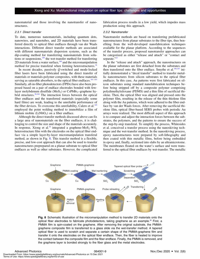
Although the direct transfer methods discussed above can fixa large area of nanomaterials on the fiber endfaces, it is chal-lenging to control the size and shape of the materials accurately.In response, Xiong et al.36 integrated a graphene-MoS2-WS2heterostructure film with the electrodes on the optical fiber end-face via a simple layer-by-layer micromanipulation transferalmethod, as shown in Fig. 8. This transfer method is a flexible,precise, and low-cost approach that can also be used to transfernanostructures preprepared on a planar substrate to optical fiberendfaces as well as other substrates. However, the complicated
fabrication process results in a low yield, which impedes massproduction using this approach.
2.3.2 Nanotransfer
Nanotransfer methods are based on transferring prefabricatednanostructures from planar substrates to the fiber tips, thus ben-efiting from the well-developed nanofabrication techniquesavailable for the planar platform. According to the sequencesof the transfer process, proposed nanotransfer approaches canbe categorized as either “release and attach” or “contact andseparate.”23
In the “release and attach” approach, the nanostructures onthe planar substrates are first detached from the substrates andthen transferred onto the fiber endface. Smythe et al.166,167 ini-tially demonstrated a “decal transfer” method to transfer metal-lic nanostructures from silicon substrates to the optical fiberendfaces. In this case, Au patterns were first fabricated on sil-icon substrates using standard nanofabrication techniques be-fore being stripped off by a composite polymer comprisingpolydimethylsiloxane (PDMS) and a thin film of sacrificial thi-olene. Then, the optical fiber was aligned and pressed onto thepolymer film, resulting in the release of the thin thiolene filmalong with the Au patterns, which were adhered to the fiber end-face by van der Waals forces. After removing the sacrificial thi-olene film, optical fiber-based SERS probes with periodic Auarrays were realized. The most difficult aspect of this approachis to compare and adjust the interaction forces between the sub-strates, the polymers, and the patterns to ensure the success ofthe step-by-step transferal. To simplify the process, Whitesideset al. conceived a transfer process using the nanoskiving tech-nique and the wet-transfer method. In the nanoskiving process,epoxy nanostructures were prepared by soft-lithography andthen coated with thin metallic films, before being embeddedin epoxy and, finally, sectioned into slabs by an ultramicrotome.The membranes floated on the water’s surface and were trans-ferred to the optical fiber endfaces by wet-transfer. The metallic
Graphene
PMMA coating
PMMA-graphene
Separation
Wet tranferring Scratching
Tapered optical fiber probe
SiO2Cu
Probe retreating
Cu
Transferring
Heating
SiO2
PMMA
removal
PMMA-grapheneGraphene
Fig. 8 Schematic illustration of the micromanipulation method to transfer 2D materials onto theoptical fiber electrodes to fabricate photodetectors, taking graphene as an example.36 First, aPMMA film is spin-coated on the graphene. After removing the original substrate, the PMMA-graphene composite film is transferred to a glass slide via the wet-transfer method. A taperedoptical fiber is used to scratch and separate a certain shape of the PMMA-graphene film andtransfer it onto the electrodes on the optical fiber endface. Then, the fiber is heated to improvethe contact between the composite film and the fiber endface. Finally, the PMMA is removed, andthe graphene layer is bonded strongly to the fiber glass and the metal electrodes.
Xiong and Xu: Multifunctional integration on optical fiber tips: challenges and opportunities
Advanced Photonics 064001-9 Nov∕Dec 2020 • Vol. 2(6)Downloaded From: https://www.spiedigitallibrary.org/journals/Advanced-Photonics on 15 Dec 2021Terms of Use: https://www.spiedigitallibrary.org/terms-of-use

nanostructures on the fiber endface were obtained after the re-moval of the epoxy by PE.168 In contrast to discrete nanoarrays,large-sized structures such as PCs can be transferred directlyusing a micromanipulation method. For example, Jung et al.169
successfully transferred a PC slab to the fiber endface using anFIB tool fitted with a micromanipulator. Similarly, Wang et al.170
released a PC nanocavity membrane from its original substrateand attached it to the fiber endface via micromanipulation usinga tapered fiber. This type of process requires high flatness ofboth the optical fiber endfaces and the nanostructured mem-branes so that sufficient van der Waals forces are obtained tobond the nanofeatures.
For the “contact and separate” approach, the optical fiberendfaces are first coated with an adhesion layer such as an epoxyor ultraviolet (UV) curable resist and then aligned and placedinto contact with the nanostructures on planar substrates.After the subsequent curing of the adhesion layer, the nanostruc-tures are separated from the original substrate and bondedstrongly to the fiber endfaces.171 Thus, Shambat et al. demon-strated a simple and rapid epoxy-based method for transferringPC cavities to optical fiber endfaces. In this case, the opticalfiber cladding area was first coated with a layer of epoxy bya sharp electrical probe on a micromanipulator stage. Afterthe optical fiber was aligned and contacted to the PC structure,it was released gradually as the epoxy cures, with the PC struc-ture adhering to the fiber endface.172,173 The micromanipulationmethod used here can prevent contamination of the optical fibercore and protect the central PC cavities. To simplify the ap-proach, Jia and Yang174–177 transferred nanohole and nanoslitarrays from Au-coated templates to optical fiber endfaces bymeans of depositing epoxy layers on the entirety of the fiberendfaces.
As with epoxy, UV glue is a popular medium used to sep-arate and transfer nanostructures to optical fibers, with thismethod operating similarly to the NIL process to a certainextent.178 For example, Lin et al. demonstrated the fabricationof plasmonic fiber probes via a UV glue-based structure trans-feral method. After a spherical packed polystyrene (PS) tem-plate had been prepared, the PS spheres were embedded in a thinUV glue layer precoated on the fiber endface and subsequentlyremoved to construct the closely arranged nanocavities.179 Withthe help of UV glue, Arce et al. successfully integrated an SOIphotonics sensor on an optical fiber endface. Notably, a layer ofwax was coated between the substrate and the structure, servingas a sacrificial layer to facilitate the separate processes.180
3 Structures and ApplicationsThe previous section introduced numerous studies in which theintegration of micro- and nanostructures onto the flat tips of op-tical fibers has been proposed. Optical fiber devices possessmany advantages, such as small size, light weight, electromag-netic immunity, and remote sensing capability. Herein, we re-view the typical structures encountered on fiber tips and theirknown and potential applications, which we have categorizedwith respect to functional structure configuration, includingthe optical functionalization of optical fibers and electrical in-tegration on optical fibers (Fig. 9).
3.1 Optical Functionalization
In recent decades, various optical structures have been fabri-cated on optical fiber tips successfully, covering diverse
applications in the fields of beam-shaping, collimation, focus-ing, signal processing, imaging, sensing, and particle trappingamong others. Considering that the optical structures integratedon the fiber tips have different sizes, shapes, dimensions, andlight–matter interaction approaches, they can be classified intotwo categories, those belonging to 3D miniature structures andthose belonging to 2D functional surfaces.
3.1.1 3D miniature structures
The diversity of applications and the requirements of compactoptical systems have driven the development of 3D miniatureoptical elements on the order of the fiber diameter. As discussedin the previous section, a variety of fabrication techniques havebeen developed to integrate minimized optical components ontooptical fiber tips, including FIB, fs laser ablation, chemical etch-ing, and two-photon direct laser writing. The following shortsections review the typical minimized 3D miniature opticalstructures integrated on fiber tips, which include optomechan-ical structures and micro-lenses.
Optomechanics. Fiber-optic optomechanics refers to the tech-nologies concerning the design and manufacture of micron-scale optomechanical structures on optical fibers. Typicaloptomechanical structures include cantilevers and suspendedmembranes forming FP cavities.Sensing. FP resonance cavities built on optical fiber tips havebeen studied extensively to produce sensors for pressure, temper-ature, vibration, and acoustics in remote, space limited, and harshenvironments. An FP cavity consists of two or more parallel re-flecting mirrors, in which interference arises due to the superpo-sition of both reflected and transmitted beams between the twoparallel surfaces. Typical fiber-optic FP interferometers consist ofan optical fiber-cavity-thin film structure, in which capillaries,coreless fibers, hollow fibers, certain fiber fusion structures(e.g., bubbles), and certain smart materials (such as microgels)are used to form resonant cavities covered with thin films suchas silica films, metal films, and 2D materials films.44–48,50,181–183
Electrical integrationNEMS / MEMS Photoelectricalconversation
Opticalmodulation
Nanoarrays
Nanomaterials
Optomechanics
Microlenses
3D miniature structures 2D functional surfaces
Fig. 9 The paradigm of multifunctional structures integrated onoptical fiber tips. The fiber tip devices were classified with respectto functional structure configuration, including (top left) the 3Dminiature micro-optics structures, (top right) 2D textured nano-optics surfaces, and (bottom) electrodes integrated on fiber tips.
Xiong and Xu: Multifunctional integration on optical fiber tips: challenges and opportunities
Advanced Photonics 064001-10 Nov∕Dec 2020 • Vol. 2(6)Downloaded From: https://www.spiedigitallibrary.org/journals/Advanced-Photonics on 15 Dec 2021Terms of Use: https://www.spiedigitallibrary.org/terms-of-use

Imaging. Iannuzzi et al.70,71,184 fabricated cantilever structures onfiber-tops by utilizing FIB and fs laser micromachining appliedfor contact mode AFM imaging. In addition, polymer-cappedoptical fiber tips were also investigated as FP interferometers,with applications including ultrasound sensors, photoacoustictransducers, and 3D endoscopy.185–189 For example, Guggenheimet al.190 proposed an optical fiber probe for ultrasound detectionbased on a planoconcave polymer microresonator with strong op-tical confinement (Q-factor > 105), which showed high ultra-sound sensitivity with an excellent broadband acoustic frequencyresponse and wide directivity. On the other hand, for ultrasoundexcitation, multiwalled carbon nanotube (MWCNT)-PDMScomposites are a typical material used for photoacoustictransducers.191,192 Using this approach, Finlay et al. reported anall-optical ultrasound transducer consisting of two optical fibersthat can generate and receive ultrasounds, respectively, and it wasapplied to real-time invasive medical imaging in vivo. The ultra-sound was generated through the photoacoustic excitation ofMWCNT-PDMS on the fiber endface via a pulsed laser, withthe returning ultrasound signal detected by a high-finesse FP cav-ity on a single-mode optical fiber. A custom-built inner transsep-tal needle with a metallic septum was used to encapsulate andisolate the two optical fibers, which was then used within thebeating heart of a pig to provide real-time views of the cardiactissue.193 Other than the above examples that used a single fiberfor excitation or reception of an ultrasound, Ansari et al. demon-strated a miniature forward-viewing 3D endoscopic probe, whichconsisted of a coherent optical fiber bundle with a mirror-polymer-mirror FP ultrasound sensor at its endfaces. The sensorcomprised 50,000 individual elements within the 3.2-mm outerdiameter of the probe, affording fine spatial sampling andhigh-resolution photoacoustic images.187
Moreover, in order to identify specific substances accurately,FP interferometers built at optical fiber tips can be integrated withmultiple kinds of nanomaterials, thus combining the characteris-tics of the nanomaterials and the features of FP cavities, whichwill be discussed further in Sec. 3.1.2. Optical fiber-basedMEMS/NEMS devices were also investigated, which will bediscussed in Sec. 3.2.1.
Microlenses. Lens systems are an integral component of appli-cations involving beam-shaping, collimation, focusing, and cou-pling and are frequently subject to restrictions relating to theirsize, shape, and dimensions, owing to the limitations of lens fab-rication techniques. Microlenses are miniaturized lenses, typi-cally involving parameters on the micrometer scale. In recentdecades, microlenses with various lens designs have been inte-grated successfully onto optical fiber tips. This has been realizedfor lens designs including planoconvex-lenses, biconvex-lenses,spherical lenses, toric lenses, and multilens composite structures,to name just a few (Fig. 10).132 The integration of small high-performance microlenses onto optical fibers requires submicrom-eter alignment accuracy relative to the fiber core, making it dif-ficult to transfer the microlenses to the fiber tip precisely.Therefore, most microlenses are processed directly on the fiberendface using methods such as FIB milling, chemical etching,3D direct laser writing, and NIL.56,59,69,133,136,139,194–198 As an exam-ple, Gissibl et al.142 demonstrated the complete process chain forhigh-performance multilens objectives on fiber endfaces withsizes of ∼100 μm, indicating its potential application in the fieldsof beam shaping, endoscopy, illumination, imaging, inspection,and microscopy on the micrometer scale. The same research team
proposed submicrometer dielectric phase masks on single-mode optical fiber endfaces for spatial beam intensity shaping[Fig. 10(a)].140 Moreover, optical tweezers have been proposedthat involve the fabrication of microstructured optical fiber end-faces, which are created using FIB milling.68,72
3.1.2 2D functional surfaces
The continuous development of nanoscience and nanotechnologymakes addressing the feasibility of optics on the nanometerscale inevitable. As mentioned above, a variety of fabricationtechniques have been explored to create nano-optical structuresdirectly on optical fiber endfaces, such as FIB milling, EBL, NIL,and SA. In contrast to micro-optical devices, nanostructures withdiscrete 2D planar nanofeatures can be transferred easily to thesurface of optical-fiber endfaces, using the so-called nanotransfermethod. To date, several typical nano-optical structures have beenintegrated on fiber endfaces successfully, such as nanomaterials,periodic nanoarrays, and metamaterials, which will be discussedin the following sections.
Nanomaterials integration. The useful properties of nanoma-terials and the features of optical fibers can be combined to pro-duce an attractive platform for various applications, such aslasing and sensing.Lasing. Pulsed fiber lasers have been applied in fields rangingfrom optical frequency metrology to nonlinear wavelength con-version and from nonlinear microscopy to investigating the dy-namic evolution of solitons.199–202 Set et al.163 presented the firstpassively mode-locked fiber lasers based on a carbon nanotube(CNT) saturable absorber. Since then, passively Q-switched andmode-locked fiber lasers have been integrated on optical fiberendfaces using various saturable absorbing nanomaterials,including NPs, CNTs, graphene, topological insulators (e.g.,Bi2Te3, Bi2Se3, Sb2Te3), transition metal dichalcogenides,black phosphorus, and material composites.126,160–162,203–213
Taking graphene as an example, the interband optical absorptionin zero-gap graphene can be easily saturated under strongexcitation due to Pauli blocking. Following this principle,Bao et al.160 demonstrated a mode-locked fiber laser for the gen-eration of ultrashort soliton pulses within the telecommunica-tions band, using atomic layer graphene as a saturable absorber.Chemosensing. Further, nanomaterials including metals, metaloxides, their composites, as well as low-dimensional materialssuch as CNT, graphene, and graphene oxides have been imple-mented for fiber-optic physical, chemical, and biologicalsensors.15,117,118,127,128,159,214–225 Incorporating the principles ofFresnel reflection, interferometers, and surface plasmon reso-nance (SPR), respectively, various nanomaterial films have beenintegrated onto fiber tips, thus demonstrating chemical sensorstailored to the detection of specific gases, VOCs, and heavymetal ions.15,214,226 Predominantly, these fiber-based sensors ex-ploit the sensing characteristics of the nanomaterials, whicheventually affect the optical structure of the optical fiber sensingsystem.
Within the last decade, toxic gases (e.g., NH3, H2S, NO2,CO2) and flammable gases (e.g., CH4, H2) have been monitoredusing these optical fiber-based chemical sensors that comprisesensitive nanomaterial films on fiber tips.215–224 For example,nanofilms of graphene oxide (GO)-based nanohybrids andporous graphene, as well as Fe3O4-graphene composite-coatedoptical fiber tips, have been investigated for the detection of am-monia (NH3) at room temperature.222,223,227 Elsewhere, ZnO NPs
Xiong and Xu: Multifunctional integration on optical fiber tips: challenges and opportunities
Advanced Photonics 064001-11 Nov∕Dec 2020 • Vol. 2(6)Downloaded From: https://www.spiedigitallibrary.org/journals/Advanced-Photonics on 15 Dec 2021Terms of Use: https://www.spiedigitallibrary.org/terms-of-use

have been embedded into a poly-methyl-methacrylate (PMMA)matrix and coated on the fiber tip for sensing H2S (at concen-trations ranging from 1 to 5 ppm) at room temperature.221
Furthermore, a lutetium bisphthalocyanine (LuPc2) dispersedmesostructured silica film has been coated on a fiber tip, whichwas sensitive to NO2 in the ppm range.224 Sensitive layers of Pd,Pd-Y, Pt-WO3, Pd capped alloys, and nanostructured α-MoO3
[Fig. 11(a)] have been coated both on fiber endfaces and fiberresonance structures, creating high sensitivity hydrogensensors.215–218,220,228,229
Similarly, VOC optical fiber sensors have been demon-strated. For example, a zeolite thin film-coated spherical opticalfiber FP cavity was investigated for sensing isopropanol, form-aldehyde, and their mixtures by monitoring the wavelength shiftof FP interference, which was induced in response to the mol-ecules of the VOCs being adsorbed onto the zeolite film.230
Alternatively, a nanopatterned GO-TiO2 film was fabricated
on fiber tips to produce a guided mode resonance structure.The structure was able to detect ethylene and methanol vaporswith sensitivities of 0.92 and 1.37 pm∕ppm, respectively.231
Elsewhere, optical fiber VOC sensors based on porous silicaxerogels have been reported using the sol–gel process, with theresulting sensors showing sensitivity toward dichloromethane,acetone, and cyclohexane.232
Beyond sensing gas molecules, various nanomaterial deco-rated fiber-optic sensors have been explored in relation to heavymetal ion (e.g., Hg2þ, Mg2þ, Pb2þ, Cd2þ) detection in liquidsolutions. For instance, by immobilizing the organic fluoro-phore Rhod-5N on the fiber tip, fluorescent sensors for the de-tection of mercury ions (Hg2þ) with a limit as low as 0.3 ppb inaqueous solution have been developed.233
Biosensing. Metallic NPs have been fabricated and transferredto fiber tips for biosensing. For example, an LSPR sensor hasbeen fabricated using spherical Au NPs on an optical fiber tip,
y-co
ordi
nate
(m
m)
z = 5.00 mm
-2
-1
0
1
2
x-coordinate (mm)-2 -1 0 1 2
z = 5.00 mm
0.0
0.2
0.4
0.6
0.8
1.0
Nor
mal
ized
inte
nsity
EXPERIMENT )b()a( EXPERIMENT
x-coordinate (mm)-2 -1 0 1 2
(a1) (a2) (a3) (a4)
(b1)
(b2)
(b3) (b4)
(b5)
(c1)
(c2)
Fig. 10 Micro-optical elements integrated on optical fiber tips. (a) Phase masks on fiber endfacesfor spatial beam intensity shaping. (a1), (a2) SEM images of a diffractive optical element on anoptical fiber endface. (a3), (a4) Measured intensity distributions for (a3) the doughnut-shaped and(a4) top-hat-shaped diffractive optical elements.140 Copyright 2016, Optical Society of America.(b) High RI Fresnel lens on a fiber endface for efficient light focusing. (b1), (b2) SEM imagesof the Fresnel lens on a fiber. (b3), (b4) Light intensity distributions of (b3) a bare single-modefiber and (b4) a fiber with Fresnel lens. (b5) The corresponding intensity profiles of the light in-tensity distributions.194 Copyright 2016, Optical Society of America. (c) Suspended polymer micror-ings on a multicore fiber endface for multiple gas sensing. (c1) SEM image of the optical tentacleon the fiber endface. (c2) Cycle tests for the sensing reversibility of the optical tentacle in threetypes of vapor.147 Copyright 2020, Optical Society of America.
Xiong and Xu: Multifunctional integration on optical fiber tips: challenges and opportunities
Advanced Photonics 064001-12 Nov∕Dec 2020 • Vol. 2(6)Downloaded From: https://www.spiedigitallibrary.org/journals/Advanced-Photonics on 15 Dec 2021Terms of Use: https://www.spiedigitallibrary.org/terms-of-use

which was applied for the detection of antibody–antigen reac-tions with a detection limit of ∼2 pg∕mL.117 Recently, as shownin Fig. 11(b), Sciacca and Monro118 exploited different metallicNPs (Au and Ag), which have distinct LSPR signatures withlimited overlap, achieving multiplexed biosensing on a singleoptical fiber probe.
Several studies have proposed optical fiber-based SERSprobes produced by depositing metallic NPs onto the fibertips.119,234–237 Recently, a double-substrate “sandwich” structurewas proposed for fiber SERS detection. First, Ag NPs were fab-ricated using the fiber surface as the SERS substrate, and thenthe fiber probe was immersed in a solution containing a mixtureof Ag NPs and target analyte molecules. The Ag NP structureson the fiber and in the solution randomly sandwich the analytemolecules in between, which enhances the electromagnetic fieldand thus produces the SERS signal. By exploiting this principle,the highly sensitive detection of R6G, proteins lysozyme andcytochrome c has been demonstrated [Fig. 11(c)].159,235
Notably, a variety of approaches for fiber-optic sensingapplications have been explored on side-polished D-shapedfibers, unclad fibers, tapered fibers, and fiber Bragg gratings,benefiting from the long matter–environment interactiondistance.15,23,114,238,239
Imaging. Nanomaterials-coated fiber endfaces can be regardedas multiple-scattering tips for imaging applications such as mi-croendoscopy. Shin et al. demonstrated 2D single-pixel imaging
using illumination via a TiO2-coated single-mode fiber andcompressed sensing acquisition. The TiO2-coated fiber endfacewas a multiple-scattering surface that produced randomly struc-tured, but deterministic, speckle patterns to illuminate the targetobject. Using a single photodetector to collect the scatteredlight, the images of the object can be reconstructed from thewavelength dependence of the speckle patterns and the totallight of the object.240
Nanoarrays integration. As discussed in Sec. 2, metallic nano-arrays with various nanofeatures have been fabricated on fiberendfaces, including periodic, quasiperiodic, or random distribu-tions of nanopillars, nanodots, nanoholes, nanodisks, and nano-gratings. These devices have been demonstrated in applicationsin numerous fields, including chemical and biological sensing,beam operations, nonlinear photonics, and optical tweezers. It isnotable that, metasurfaces (MSs), as 2D artificial electromag-netic media on the subwavelength scale, can guide and controlthe propagation of electromagnetic waves by engaging reso-nance excitations such as localized plasmonic modes.241–243
The integration of MSs and optical fiber technologies facilitatesthe control of light using nanoscale arrays on the fiber endface,which can be applied in the fields of communications, signalprocessing, imaging, as well as sensing.Sensing. Light–matter interaction occurring in subwavelengthmetallic nanostructures can be enhanced by several orders of
Fig. 11 Optical fiber-based SERS probes. (a) Schematic depiction of the measurement setup forcharacterizing an SERS probe. Inset: SEM image of an array of Au optical antennas on a fiberendface.166 Copyright 2009, American Chemical Society. (b) SEM image of the Ag-coated nano-pillar array on a fiber endface used for SERS.96 Copyright 2012, Optical Society of America.(c) SEM image of nanoscale honeycomb structures on a fiber endface for SERS.66 Copyright2005, Optical Society of America. (d) SERS-on-a-tip probes based on a nanoarray on an opticalfiber endface.145 (d1) Schematic illustration of the mechanism for Raman scattering enhancement.(d2), (d3) SEM image of the cross-spike array on an optical fiber tip. Copyright 2020, WILEY-VCHVerlag GmbH & Co. KGaA, Weinheim.
Xiong and Xu: Multifunctional integration on optical fiber tips: challenges and opportunities
Advanced Photonics 064001-13 Nov∕Dec 2020 • Vol. 2(6)Downloaded From: https://www.spiedigitallibrary.org/journals/Advanced-Photonics on 15 Dec 2021Terms of Use: https://www.spiedigitallibrary.org/terms-of-use

magnitude via LSPR. Therefore, every alteration at the sensorsurface, such as changing the RI, temperature, or the bindingof molecules, results in the resonant wavelength(s) shifting.According to this principle, numerous optical fiber-basedRI sensors for the quantitative analysis of chemical reactionsand biological interactions have been demonstrated, basedon arrays of metallic nanodisks,87 nanodots,86,113 nano-holes,76,77,175,176,244–246 nanoslits and nanogratings,95,174,247–249 nano-pillars and nanorods,250,251 nanorings,89 nanotrimers,252 andmetal–dielectric nanocrystals.88,112,121 For example, Jia et al.174
constructed plasmonic optical fibers by transferring patternedmetal nanostructures onto optical fiber endfaces, which showednarrow linewidths (6.6 nm) and a high figure of merit (60.7).The plasmonic fiber probe was first characterized as an RI sen-sor using different concentrations of NaCl solution with a trans-mission sensitivity of 595 nm per refractive index unit. Then, theprobe performed label-free and real-time biosensing using theimmunoassay of the antigen–antibody, revealing a detectionlimit of 8.5 pgmm−2. Recently, Aliberti et al.253–255 integratedmicrogels onto a plasmonic nanohole array prefabricated ona fiber endface, which concentrated the target molecule and thusenhanced the optical response.
Other than via the LSPR principle, nanostructures integratedon fiber endfaces have been applied as chemo- and biosensorsbased on SERS. In general, the SERS effect can lead to amillionfold enhancement of the Raman scattering intensityfor molecules, which is attributed to either the electromagneticenhancement or the chemical interaction between the SERS ac-tive surface and the attached target molecules. In recent decades,optical fiber-based SERS probes have been exploited by inte-grating various kinds of nanoarrays, including periodic arraysof nanoscale optical antennas [Fig. 11(a)],166 nanorods andnanopillars [Fig. 11(b)],96 nanoholes,73 nanocavities,179 and hon-eycombs [Fig. 11(c)],66 as well as randomly distributed arrays ofnanorods,256 NP clusters,120 and replicas of nanotemplates.102,109
Recently, as shown in Fig. 11(d), Kim et al.145 used two-photon
polymerization and subsequent metallization to fabricate threetypes of nanoarrays on the endfaces of optical fibers, presentinga fiber-optic SERS probe for the rapid detection of bacteria. Theprobes showed a detection limit of R6G of 10−7 mol∕L, whilethe enhancement factor was measured as 1300, which was thenapplied for rapid SERS detection of live Escherichia coli cellswith Raman integration time ranging from milliseconds to sec-onds. Consales et al.257 used phase-gradient plasmonic MS onthe optical fiber tip to detect biomolecular interactions with alimit of detection of the order of a few ngmL−1.Beam shaping and operation. In addition to the nanostructuresmentioned above, metallic nanogratings on optical fiber endfa-ces exhibit unique optical properties due to the surface plasmonpolaritons that result from the light confined in optical fibersinteracting with the subwavelength nanograting. These nano-gratings can be utilized as optical filters,258,259 amplifiers,258 po-larizers,85 beam splitters,107 and metallic Fresnel zone plates,260
as well as in applications requiring waveguide coupling,106
Bessel beam generation,74 wavelength-division-multiplexingsignal monitoring,81 and wavelength-dependent off-axis direc-tional beaming.261 In addition to that, meta-fiber tips are alsowidely demonstrated for beam shaping and operation. For ex-ample, Principe et al.78 proposed a phase-gradient plasmonic MSintegrated on a fiber tip [Fig. 12(a)], enabling an impingingbeam to be guided in desired directions. A 50-nm Au layer withdifferent rectangular nanoholes was patterned in the plane ofthe fiber endface. By tuning the nanohole sizes appropriatelyto correspond to the resonance frequency, an arbitrary phase(within the full 2π range) can be induced in the transmitted/re-flected components with suitable polarization. Specifically,interactions between ordinary and anomalous beams can berealized by adjusting the angles of the prototype according tothe array-induced phase-matching mechanism. This MT con-figuration was applied for beam polarization and phase gradientcontrol.262 Similarly, Yang et al.263 reported an optical metalenspatterned on the core area of a PCF endface to be used for light
(a1)
Single-mode fiber core
Ordinary
Anomalous
Metasurface
Incidentbeam
x
z
y
(a2)
(a3)
n fiber
next
t
r
Phase gradient
x
x
z
x
zy
ly
lx
L1
L2
45°h
Output γ
Output δ
Input β
Input α
Fiber
Meta-surface
Fiber
(b)
Fig. 12 Metasurfaces on optical fiber tips. (a) An optical fiber MT for beam steering and coupling.(a1) Schematic view of the MT with a plasmonic MS fabricated on the endface. (a2) Illustration ofthe MT operating principle. (a3) Geometry of the rectangular nanoaperture realized in an Aulayer.78 Copyright 2016, Springer Nature. (b) Schematic illustration of an MS-covered optical fibertip for all-optical signal modulation based on coherent absorption. The insets are SEM images ofthe device, black scale bar: 100 μm, gray scale bar: 1 μm. Copyright 2018, Springer Nature.
Xiong and Xu: Multifunctional integration on optical fiber tips: challenges and opportunities
Advanced Photonics 064001-14 Nov∕Dec 2020 • Vol. 2(6)Downloaded From: https://www.spiedigitallibrary.org/journals/Advanced-Photonics on 15 Dec 2021Terms of Use: https://www.spiedigitallibrary.org/terms-of-use

focusing at communications wavelengths, which showed amaximum enhanced optical intensity as large as 234% at thefocal point of the lens. Moreover, Xomalis et al.264 reported afully fiberized and packaged optical switching meta-fiber devicebased on coherently controlled absorption [Fig. 12(b)]. Withina coherent fiber network, logical functions of XOR, NOT,and AND were performed at wavelengths between 1530 and1565 nm, indicating potential in the field of coherent and quan-tum information networks.Optical tweezers. Optical tweezers have been instrumental formanipulating micro- and NPs accurately and noninvasively.Conventional optical tweezers are used typically to trap andmanipulate micron-scale objects, while they are incapable oftrapping nanoscale objects directly. This is because trappingNPs requires an ultrahigh optical power to increase the opticalforces, which leads to photothermal issues. Moreover, owing tothe diffraction limit, the size of the optical trap is often hundredsof times greater than the size of NPs. To overcome the weakoptical forces and photothermal issues accompanying conven-tional optical tweezers, plasmonic optical tweezers, which havestrong field gradients that can trap and manipulate NPs withlower optical power levels, have been developed.265–269 Recently,plasmonic optical tweezers have been integrated on the endfacesof optical fibers, enabling the 3D manipulation of trapped nano-scale particles.270 In pioneering work proposed by Berthelotet al.,271 a bowtie-shaped plasmonic aperture was fabricatedat the endface of a tapered Au-coated optical fiber, demonstrat-ing near-field nanotweezers for 3D optical trapping, manipula-tion, and trapping status monitoring of individual 50-nmdielectric particles. The trapped objects were able to be movedover distances measuring tens of micrometers in several minutes
using very low in-trap intensities. Similarly, Gelfand et al.272
built a double nanohole aperture on an Au-coated endface ofa nontapered optical fiber, demonstrating the trapping andmonitoring of individual 20- and 40-nm diameter PS spheres(Fig. 13). To improve the mode matching and optical couplingof the plasmonic structure, Saleh et al.273 designed a fiber opticplasmonic tweezer with subwavelength coaxial geometry,which was fabricated on a fiber endface and can trap sub-10-nm dielectric particles.Imaging. In the field of imaging, optical aberrations and thetrade-off between transverse resolution and depth of focus aretechnological challenges. Pahlevaninezhad et al.274 integrated ametalens into a fiber-based nano-optic endoscope to modify thephase of incident light at the subwavelength level, realizingnear diffraction-limited imaging by negating nonchromaticaberrations.
3.2 Electrical Integration
Owing to the limitations of the material characteristics ofoptical fibers (most often SiO2), they do not possess electronicand optoelectronic functions, which limits their application.In the 2000s, researchers tried to integrate different materialsand microstructures into optical fiber configurations whiledrawing the fiber, making fibers that can see, hear, sense, andcommunicate.1–12 This field of “multimaterial fibers” arousesgreat industrial interest but also faces some technological chal-lenges. In this section, we discuss several recently proposed de-vice designs for electrical integration on optical fiber endfaces,which use commercially available standard optical fibers andsimpler fabrication methods.
Fig. 13 Optical tweezers based on a double nanohole on the fiber endface.272 (a) SEM image ofthe active region of the fiber. (b) SEM image of the finished double nanohole milled in the activeregion of the fiber. (c) Schematic illustration of the characterization setup of the optical tweezers.(d), (e) Trapping events for individual 40- and 20-nm diameter PS spheres, respectively, which aredetected via the change in transmission. Copyright 2014, Optical Society of America.
Xiong and Xu: Multifunctional integration on optical fiber tips: challenges and opportunities
Advanced Photonics 064001-15 Nov∕Dec 2020 • Vol. 2(6)Downloaded From: https://www.spiedigitallibrary.org/journals/Advanced-Photonics on 15 Dec 2021Terms of Use: https://www.spiedigitallibrary.org/terms-of-use

3.2.1 NEMS on fiber
Optical NEMSs are optical systems with adjustable or control-lable mechanical components and are widespread in the fields ofsensing and communications. Since the discovery of graphene,with its unique electronic and mechanical properties, several in-vestigations have explored the integration of graphene NEMSon optical fiber tips. As shown in Fig. 14, Zheng et al.67 dem-onstrated a miniature optical fiber current sensor based on a qua-sistatic graphene NEMS. The optical fiber was etched by an HF-water solution, forming a hole in the center of the fiber tip due tothe faster etching speeds at the core area. Subsequently,a pair of Au electrodes was fabricated on opposite sides ofthe hole, which was covered by a free-standing graphene mem-brane. Due to the negative thermal expansion effect of graphene,the shape of the graphene membrane changed with the current-induced variation of temperature, which was detected using thereflection spectra of the sensor. An equivalent device configu-ration has been demonstrated for magnetic field sensing basedon the Lorentz force.275 Similarly, Liu et al.49 fabricated an all-in-fiber current-driven Lorentz force magnetometer based on anNEMS consisting of a fiber-capillary-graphene-gold hybridstructure. The difference is that the graphene membrane wasused principally to support a 100-nm-thick Au layer, whichhas a higher light reflection ratio, lower resistance, and betterrepeatability. The shape of the suspended graphene-gold-composite membrane changed with the applied Lorentz force,which was related to the propagating current in the magneticfield. By monitoring the reflection spectra of the sensor, thechange in the magnetic field was detected with a sensitivityof 0.64 pm∕mT and a response time of ∼0.1 s.
3.2.2 Photoelectrical conversion
The integration of optoelectronic materials onto optical fibers isan effective way to overcome the limitations inherent to opticalfiber materials. Recently, various kinds of photoelectric materi-als, such as quantum dots, nanotubes, perovskites, 2D materials,organic optoelectronic materials, and multiple-material hetero-structures, have been exploited for on chip phototransistors,photodetectors, sensors, and solar cells among others.276–280
Photodetection. Similar to on-chip configurations, fiber-based photodetectors have been demonstrated successfully.As mentioned in Sec. 2.1.2, Chen et al.38 developed a simpleapproach for fabricating electrodes on fibers with relatively highprecision using lapping films and a tapered tungsten needle toconstruct two electrodes on opposite fiber sidewalls and facets.
Then, a film of few-layer molybdenum disulfide (MoS2) wasbonded directly to the fiber electrode [Fig. 15(a)], demonstratingan all-in-FPD with a photoresponsivity of ∼0.6 AW−1 at an in-cident light power of ∼4.4 nW. Owing to the spatial asymmetryof the electrodes, the FPD worked at zero bias. To improve pho-todetection performance, FPDs with integrated perovskites-graphene hybrid structures have been proposed, as shown inFig. 15(b). Aided by the high carrier mobility inside grapheneand the high photosensitivity of perovskites, the FPD showed aphotoresponsivity as high as 2 × 10⁴ AW−1.164
However, these FPDs can only detect visible light because ofthe limitations of the materials, hindering their application atcommunication frequencies. To resolve this issue, Xiong et al.36
deployed a simple layer-by-layer transfer method to create amicroscale multilayer graphene-MoS2-WS2 heterostructurefilm on fiber tip electrodes [Fig. 15(c)]. Due to the strong lightabsorption and the built-in electric field of the heterostructure,the FPD exhibits an ultrahigh photoresponsivity of∼6.6 × 10⁷ AW−1 and a relatively fast response time of ∼7 msat a wavelength of 400 nm. Moreover, the type-II staggeredband alignments in the MoS2-WS2 heterostructure enablesthe FPD to sense infrared light, displaying a photoresponsivityof ∼17.1 AW−1 at 1550 nm. Recently, a 2D covalent organicframework (COF)-graphene film was successfully integratedonto fiber electrodes using a similar approach, with the finalstructure utilized for gas sensing applications [Fig. 15(d)].37
We envision an all-in-fiber phototransistor with a three-electrode configuration on the fiber tip, consisting of a pair ofdrain-source electrodes and a transparent back gate electrode,which can adjust the semiconductor properties by controlling thegate voltage. This configuration should satisfy applications inboth photoelectrical conversion and electro-optical modulation.
Photoelectrochemical analysis. The photoelectrochemical(PEC) process refers to the photoelectrical conversion of photo-active materials under illumination that forms electron–holepairs at their interface, which will cause the oxidation–reductionreaction of the molecules or ions.281 Owing to their light-guidingproperties, optical fibers are an ideal platform for monitoringPEC reactions. For example, Esquivel et al. developed a TiO2-based photoanode on the surface of a semiconductive modifiedoptical fiber, thus allowing the construction of a PEC reactor viaan internally illuminated approach. Using this configuration,the electro-Fenton photoelectrocatalytic oxidation process wasstudied to achieve total color removal of the azo dye Orange II(15 mgL−1) and a 57% removal of total organic carbon within60 min of the degradation time.282 In addition, electro-opticalnanoprobes based on tapered optical fibers may have applicationprospects in single-cell analysis.283
3.2.3 Optical modulation
The light propagating through a certain material can be modu-lated by external environmental factors, such as electric fields,optical fields, magnetic fields, temperature, and mechanicalstrain.284,285 The small core and the engineerable endface orsidewall of optical fibers can offer tight optical confinementfor enhancing light–material interactions, thus making opticalfibers an ideal platform on which to develop modulators andlasers.17,286,287
Thermo-optic. With improvements to the processes used toattach electrodes on optical fiber tips, it is possible to develop
Current
Lorentz forceMagnetic field
Capillary
Optical fiberElectrodes
(a) (b)
Fig. 14 NEMS on fiber tips. (a) Schematic of the optical fibermagnetometer based on a graphene NEMS. (b) Microscope im-age of the endface of the fiber sensor.
Xiong and Xu: Multifunctional integration on optical fiber tips: challenges and opportunities
Advanced Photonics 064001-16 Nov∕Dec 2020 • Vol. 2(6)Downloaded From: https://www.spiedigitallibrary.org/journals/Advanced-Photonics on 15 Dec 2021Terms of Use: https://www.spiedigitallibrary.org/terms-of-use

electro-optic and thermo-optic modulators on the fiber tips. Forexample, Li et al. demonstrated the active modulation of thenonlinear optical properties of a graphene-fiber-integrated de-vice by varying the temperature of a graphene sheet electrically.The device was fabricated by bonding multilayer graphene di-rectly onto a pair of fiber tip electrodes, with the result that theyacted as a nanoheater as well as an adjustable saturable absorber.By tuning the applied electrical current from 0 to 9 mA, thetemperature of the graphene was altered from ∼300 to ∼900 K,thus modifying the nonlinear optical absorption of the graphenefrom 2.3% to 0.9%. This graphene-based optical modulator wasincorporated into a fiber laser circuit to demonstrate the control-lable fiber laser’s operation state (mode-locked or continuous-wave) and pulse.
Magneto-optic. The electron spin of nitrogen-vacancy (NV)color centers in diamonds enables the highly sensitive detectionof weak magnetic fields, which can be manipulated by a fre-quency-modulated microwave field and initialized via laserradiation from the fiber core. Following this principle, Fedotovet al. reported optical fiber magnetic field imaging probes byattaching diamond microcrystals with NV centers to the fibertip and integrating microwave transmission lines along thefibers. The 2D magnetic field was imaged by the probe, using
the photoluminescence spin-readout return from the NVcenters.288–291
In addition to advancements concerning the complexity offiber tip electrode structures, high performance all-in-fiber de-vices, such as modulators, phototransistors, and Hall magneticfield sensors, will be developed in the future.
4 Conclusions and OutlookLOF devices have made great progress so far in almost all as-pects, ranging from theoretical calculation and device configu-ration design to fabrication techniques and measuring methods,with the ultimate aim of realizing integrated and miniaturizedall-fiber systems. Growing technological demands bring greatopportunities to explore new approaches for fiber functionaliza-tion and help the as-yet-unresolved challenges to be sur-mounted. The main challenge is to develop mass productionprocesses and equipment for the integration of materials andstructures on the platform of optical fiber endfaces, with reducedcosts and increased yields. Meanwhile, the integration of certaincomplex traditional photonic and optoelectronic systems isanother significant obstacle.
As regards future prospects, several trends and directions thatshow particular promise in this field include:
(b1) (b2) (b3)
(b4)
e-
e-
e-
Optical fiber
AuCOF-graphene
MoS2
Electrode
Electrode
MoS2
(a1) (a2)
(a3)
(c1) (d)(c2)
Vds
Ids
(c3)
Fig. 15 All-in-FPD. (a) FPD integrated with a film of MoS2.38 (a1) Schematic of the FPD with a
MoS2 film deposited above the electrodes. Inset: The cross-sectional part of the FPD and themeasurement setup. (a2) The optical microscope image of the FPD. The scale bar is 20 μm.(a3) The SEM image of the FPD. The scale bar is 50 μm. Reproduced with permission fromthe Royal Society of Chemistry. (b) High-sensitivity FPD with an integrated CsPbBr3-graphenehybrid structure.164 (b1), (b2) Schematic of the materials structures and device configuration ofthe FPD. (b3), (b4) Photograph and microscope image of an FPD. The scale bar is 20 μm.Copyright 2017, Optical Society of America. (c) Broadband FPD based on a graphene-MoS2-WS2 heterostructure.36 (c1), (c2) Schematic representation of the FPD. (c3) SEM imageof the FPD. The scale bar is 20 μm. Copyright 2018, WILEY-VCH Verlag GmbH & Co. KGaA,Weinheim. (d) Schematic view of the COF-graphene-based FPD, which can be used as a gassensor. Inset: The gas molecule absorption and charge transfer at the surface of the COF-graphene film.37 Copyright 2020, WILEY-VCH Verlag GmbH & Co. KGaA, Weinheim.
Xiong and Xu: Multifunctional integration on optical fiber tips: challenges and opportunities
Advanced Photonics 064001-17 Nov∕Dec 2020 • Vol. 2(6)Downloaded From: https://www.spiedigitallibrary.org/journals/Advanced-Photonics on 15 Dec 2021Terms of Use: https://www.spiedigitallibrary.org/terms-of-use

– First, multifunctional integration of traditional optoelec-tronic devices, both active and passive, onto fiber tips, therebyachieving a complete all-fiber module for light generation orsignal processing.
– Second, the integration of complex electrode structuresand auxiliary circuits on optical fiber endfaces, which can beapplied as high-speed optical modulators, phototransistors,and sensors.
– Third, the integration of free space optical systems on fiberendfaces, thus realizing multiple functional all-fiber systemssuch as ultrathin imaging systems or spectrum conversionsystems.
– Fourth, the integration of micro- and nanostructures on theendface of specific optical fibers (e.g., PCFs), realizing diversi-fied functions that an ordinary optical fiber does not possess.
– Finally, the preparation of functional modules with re-duced sizes onto the subwavelength-scale optical fiber tipsfor cell-level detection and in vivo biochemical monitoring.
Acknowledgments
This work was sponsored by the National Natural ScienceFoundation of China (61925502 and 61535005) and theNational Key R&D Program of China (2017YFA0303700and 2017YFA0700503). We thank Professor J. H. Chen for helpin the preparation of the manuscript. The authors declare nocompeting interests.
References
1. A. F. Abouraddy et al., “Towards multimaterial multifunctionalfibres that see, hear, sense and communicate,” Nat. Mater. 6,336–347 (2007).
2. M. Bayindir et al., “Integrated fibres for self-monitored opticaltransport,” Nat. Mater. 4, 820–825 (2005).
3. O. Shapira et al., “Surface-emitting fiber lasers,” Opt. Express14(9), 3929–3935 (2006).
4. A. Bedeloglu et al., “A photovoltaic fiber design for smarttextiles,” Text. Res. J. 80(11), 1065–1074 (2009).
5. N. Podoliak et al., “Design of dual-core optical fibers withNEMS functionality,” Opt. Express 22(1), 1065–1076 (2014).
6. A. Canales et al., “Multifunctional fibers for simultaneousoptical, electrical and chemical interrogation of neural circuitsin vivo,” Nat. Biotechnol. 33, 277–284 (2015).
7. S. Egusa et al., “Multimaterial piezoelectric fibres,” Nat. Mater.9, 643–648 (2010).
8. M. Fokine et al., “Integrated fiber Mach–Zehnder interferometerfor electro-optic switching,”Opt. Lett. 27(18), 1643–1645 (2002).
9. W. Yan et al., “Microstructure tailoring of selenium-core multi-material optoelectronic fibers,” Opt. Mater. Express 7(4), 1388–1397 (2017).
10. W. Yan et al., “Semiconducting nanowire-based optoelectronicfibers,” Adv. Mater. 29(27), 1700681 (2017).
11. W. Yan et al., “Advanced multimaterial electronic and optoelec-tronic fibers and textiles,” Adv. Mater. 31(1), 1802348 (2019).
12. W. Yan et al., “Thermally drawn advanced functional fibers: newFrontier of flexible electronics,” Mater. Today 35, 168–194(2020).
13. L. Tong et al., “Subwavelength-diameter silica wires for low-lossoptical wave guiding,” Nature 426, 816–819 (2003).
14. J.-H. Chen, D.-R. Li, and F. Xu, “Optical microfiber sensors:sensing mechanisms, and recent advances,” J. Lightwave Technol.37(11), 2577–2589 (2019).
15. D. Pawar and S. N. Kale, “A review on nanomaterial-modifiedoptical fiber sensors for gases, vapors and ions,”Mikrochim. Acta186, 253 (2019).
16. H. Chen et al., “Review and perspective: sapphire optical fibercladding development for harsh environment sensing,” Appl.Phys. Rev. 5(1), 011102 (2018).
17. E. J. Lee et al., “Active control of all-fibre graphene devices withelectrical gating,” Nat. Commun. 6, 6851 (2015).
18. J. D. Zapata et al., “Efficient graphene saturable absorbers onD-shaped optical fiber for ultrashort pulse generation,” Sci.Rep. 6, 20644 (2016).
19. J. L. Kou et al., “Microfiber-based Bragg gratings for sensingapplications: a review,” Sensors 12(7), 8861–8876 (2012).
20. S. Pissadakis, “Lab-in-a-fiber sensors: a review,” Microelectron.Eng. 217, 111105 (2019).
21. M. Pisco and A. Cusano, “Lab-on-fiber technology: a roadmaptoward multifunctional plug and play platforms,” Sensors 20(17),4705 (2020).
22. Q. Wang and L. Wang, “Lab-on-fiber: plasmonic nano-arrays forsensing,” Nanoscale 12(14), 7485–7499 (2020).
23. P. Vaiano et al., “Lab on fiber technology for biological sensingapplications,” Laser Photonics Rev. 10(6), 922–961 (2016).
24. A. Ricciardi et al., “Lab-on-fiber technology: a new vision forchemical and biological sensing,” Analyst 140(24), 8068–8079(2015).
25. G. Kostovski, P. R. Stoddart, and A. Mitchell, “The optical fibertip: an inherently light-coupled microscopic platform for micro-and nanotechnologies,” Adv. Mater. 26(23), 3798–3820 (2014).
26. M. Consales, M. Pisco, and A. Cusano, “Lab-on-fiber technol-ogy: a new avenue for optical nanosensors,” Photonic Sensors2, 289–314 (2012).
27. R. He et al., “Integration of gigahertz-bandwidth semiconductordevices inside microstructured optical fibres,” Nat. Photonics6, 174–179 (2012).
28. A. F. Abouraddy et al., “Large-scale optical-field measure-ments with geometric fibre constructs,” Nat. Mater. 5, 532–536(2006).
29. R. Raabe et al., “No enhancement of fusion probability by theneutron halo of 6He,” Nature 431, 823–826 (2004).
30. B. Temelkuran et al., “Wavelength-scalable hollow optical fibreswith large photonic bandgaps for CO2 laser transmission,” Nature420, 650–653 (2002).
31. S. A. Maier, Plasmonics: Fundamentals and Applications,Springer (2007).
32. K. I. Mullen and K. T. Carron, “Surface-enhanced Raman spec-troscopy with abrasively modified fiber optic probes,” Anal.Chem. 63(19), 2196–2199 (1991).
33. W. H. C. Viets, “Comparison of fibre-optic SERS sensors withdifferently prepared tips,” Sens. Actuators B 51(1–3), 92–99(1998).
34. T. Grosjean et al., “Fiber microaxicons fabricated by a polishingtechnique for the generation of Bessel-like beams,” Appl. Opt.46(33), 8061–8067 (2007).
35. C. Li et al., “Manipulation of nonlinear optical properties of gra-phene bonded fiber devices by thermally engineering Fermi-Diracdistribution,” Adv. Opt. Mater. 5(21), 1700630 (2017).
36. Y.-F. Xiong et al., “Broadband optical-fiber-compatible photo-detector based on a graphene-MoS2-WS2 heterostructure witha synergetic photogenerating mechanism,” Adv. Electron. Mater.5(1), 1800562 (2019).
37. Y. Xiong et al., “Ultrahigh responsivity photodetectors of 2Dcovalent organic frameworks integrated on graphene,” Adv. Mater.32(9), 1907242 (2020).
38. J. H. Chen et al., “Towards an all-in fiber photodetector by di-rectly bonding few-layer molybdenum disulfide to a fiber facet,”Nanoscale 9(10), 3424–3428 (2017).
39. F. A. Bruno et al., “Opto-mechanical lab-on-fiber accelerome-ters,” J. Lightwave Technol. 38(7), 1998–2009 (2020).
40. S. V. Beekmans et al., “Minimally invasive micro-indentation:mapping tissue mechanics at the tip of an 18G needle,” Sci. Rep.7, 11364 (2017).
Xiong and Xu: Multifunctional integration on optical fiber tips: challenges and opportunities
Advanced Photonics 064001-18 Nov∕Dec 2020 • Vol. 2(6)Downloaded From: https://www.spiedigitallibrary.org/journals/Advanced-Photonics on 15 Dec 2021Terms of Use: https://www.spiedigitallibrary.org/terms-of-use

41. H. van Hoorn et al., “Local dynamic mechanical analysis forheterogeneous soft matter using ferrule-top indentation,” SoftMatter 12(12), 3066–3073 (2016).
42. M. Pisco et al., “Opto-mechanical lab-on-fibre seismic sensorsdetected the Norcia earthquake,” Sci. Rep. 8, 6680 (2018).
43. J.-Y. Rauch et al., “Smallest microhouse in the world, assembledon the facet of an optical fiber by origami and welded in theμRobotex nanofactory,” J. Vac. Sci. Technol. A 36, 041601(2018).
44. F. Guo et al., “High-sensitivity, high-frequency extrinsic Fabry–Perot interferometric fiber-tip sensor based on a thin silverdiaphragm,” Opt. Lett. 37(9), 1505–1507 (2012).
45. J. Ma et al., “High-sensitivity fiber-tip pressure sensor withgraphene diaphragm,” Opt. Lett. 37(13), 2493–2495 (2012).
46. Y. Wang et al., “Compressible fiber optic micro-Fabry–Perotcavity with ultra-high pressure sensitivity,” Opt. Express 21(12),14084–14089 (2013).
47. J. Xu et al., “Suppression of parasitic interference in a fiber-tipFabry–Perot interferometer for high-pressure measurements,”Opt. Express 26(22), 28178–28186 (2018).
48. Z. Yizheng and W. Anbo, “Miniature fiber-optic pressure sen-sor,” IEEE Photonics Technol. Lett. 17(2), 447–449 (2005).
49. Z.-Y. Liu, H.-Q. Cao, and F. Xu, “Fiber-optic Lorentz force mag-netometer based on a gold-graphene composite membrane,”Appl. Phys. Lett. 112(20), 203504 (2018).
50. Y. Zhao et al., “Optical fiber axial contact force sensor based onbubble-expanded Fabry–Pérot interferometer,” Sens. Actuators A272, 318–324 (2018).
51. K.-C. Fan et al., “Experimental study of fabricating a microballtip on an optical fibre,” J. Opt. A Pure Appl. Opt. 8(9), 782–787(2006).
52. L. Collot et al., “Very high-Q whispering-gallery mode reso-nances observed on fused silica microspheres,” Europhys. Lett.23(5), 327–334 (1993).
53. M. L. Gorodetsky, A. A. Savchenkov, and V. S. Ilchenko,“Ultimate Q of optical microsphere resonators,” Opt. Lett. 21(7),453–455 (1996).
54. M. Kimura and K. Toshima, “Vibration sensor using optical-fibercantilever with bulb-lens,” Sens. Actuators A 66(1–3), 178–183(1998).
55. J. Laine, B. E. Little, and H. A. Haus, “Etch-eroded fiber couplerfor whispering-gallery-mode excitation in high-Q silica micro-spheres,” IEEE Photonics Technol. Lett. 11(11), 1429–1430(1999).
56. S.-K. Eah, W. Jhe, and Y. Arakawa, “Nearly diffraction-limitedfocusing of a fiber axicon microlens,” Rev. Sci. Instrum. 74(11),4969–4971 (2003).
57. H. J. Kbashi, “Fabrication of submicron-diameter and taper fibersusing chemical etching,” J. Mater. Sci. Technol. 28(4), 308–312(2012).
58. T. Saiki et al., “Tailoring a high-transmission fiber probe forphoton scanning tunneling microscope,” Appl. Phys. Lett. 68,2612–2614 (1996).
59. G. Eisenstein and D. Vitello, “Chemically etched conical micro-lenses for coupling single-mode lasers into single-mode fibers,”Appl. Opt. 21(19), 3470–3474 (1982).
60. T. Yatsui, M. Kourogi, and M. Ohtsu, “Increasing throughput ofa near-field optical fiber probe over 1000 times by the use of atriple-tapered structure,” Appl. Phys. Lett. 73(15), 2090–2092(1998).
61. T. Saiki and K. Matsuda, “Near-field optical fiber probe opti-mized for illumination–collection hybrid mode operation,” Appl.Phys. Lett. 74(19), 2773–2775 (1999).
62. P. Hoffmann, B. Dutoit, and R.-P. Salathe, “Comparison of me-chanically drawn and protection layer chemically etchedopticalfiber tips,” Ultramicroscopy 61(1–4), 165–170 (1995).
63. S. K. Mondal et al., “Optical fiber nanoprobe preparation fornear-field optical microscopy by chemical etching under surface
tension and capillary action,” Opt. Express 17(22), 19470–19475(2009).
64. K. Maruyama et al., “Fabrication and characterization of a nano-meter-sized optical fiber electrode based on selective chemicaletching for scanning electrochemical/optical microscopy,” Anal.Chem. 78(6), 1904–1912 (2006).
65. Z. Wang et al., “Optically addressable array of optomechanicallycompliant glass nanospikes on the endface of a soft-glass pho-tonic crystal fiber,” ACS Photonics 6(11), 2942–2948 (2019).
66. D. J. White and P. R. Stoddart, “Nanostructured optical fiber withsurface-enhanced Raman scattering functionality,” Opt. Lett.30(6), 598–600 (2005).
67. B.-C. Zheng et al., “Miniature optical fiber current sensor basedon a graphene membrane,” Laser Photonics Rev. 9(5), 517–522(2015).
68. S. Cabrini et al., “Axicon lens on optical fiber forming opticaltweezers, made by focused ion beam milling,” Microelectron.Eng. 83(4–9), 804–807 (2006).
69. F. Schiappelli, “Efficient fiber-to-waveguide coupling by a lenson the end of the optical fiber fabricated by focused ion beammilling,” Microelectron. Eng. 73-74, 397–404 (2004).
70. D. Iannuzzi et al., “Fiber-top atomic force microscope,” Rev. Sci.Instrum. 77(10), 106105 (2006).
71. D. Iannuzzi et al., “Monolithic fiber-top sensor for critical envi-ronments and standard applications,” Appl. Phys. Lett. 88(5),053501 (2006).
72. C. Liberale et al., “Miniaturized all-fibre probe for three-dimensional optical trapping and manipulation,” Nat. Photonics1, 723–727 (2007).
73. G. F. S. Andrade et al., “Surface-enhanced resonance Ramanscattering (SERRS) using Au nanohole arrays on optical fibertips,” Plasmonics 8, 1113–1121 (2013).
74. S. Kang et al., “Subwavelength plasmonic lens patterned on acomposite optical fiber facet for quasi-one-dimensional Besselbeam generation,” Appl. Phys. Lett. 98(24), 241103 (2011).
75. Y. Zhao, “All-fiber vibration sensor based on nano-wire gridpolarizer,” Opt. Eng. 51(5), 050504 (2012).
76. A. Dhawan and J. F. Muth, “Engineering surface plasmon basedfiber-optic sensors,” Mater. Sci. Eng. B 149(3), 237–241 (2008).
77. A. Dhawan, M. D. Gerhold, and J. F. Muth, “Plasmonic struc-tures based on subwavelength apertures for chemical and biologi-cal sensing applications,” IEEE Sens. J. 8(6), 942–950 (2008).
78. M. Principe et al., “Optical fiber meta-tips,” Light Sci. Appl. 6,e16226 (2017).
79. V. Savinov and N. I. Zheludev, “High-quality metamaterial dis-persive grating on the facet of an optical fiber,” Appl. Phys. Lett.111(9), 091106 (2017).
80. A. Micco et al., “Optical fiber tip templating using direct focusedion beam milling,” Sci. Rep. 5, 15935 (2015).
81. W. Shin et al., “Microstructured fiber end surface grating forcoarse WDM signal monitoring,” IEEE Photonics Technol.Lett. 19(8), 550–552 (2007).
82. J. K. Kim et al., “Fabrication of micro Fresnel zone plate lenson a mode-expanded hybrid optical fiber using a femtosecondlaser ablation system,” IEEE Photonics Technol. Lett. 21(1),21–23 (2009).
83. X. Lan et al., “Surface-enhanced Raman-scattering fiber probefabricated by femtosecond laser,” Opt. Lett. 34(15), 2285–2287(2009).
84. X. Ma et al., “Surface-enhanced Raman scattering sensor on anoptical fiber probe fabricated with a femtosecond laser,” Sensors10(12), 11064–11071 (2010).
85. Y. Lin, J. Guo, and R. G. Lindquist, “Demonstration of an ultra-wideband optical fiber inline polarizer with metal nano-grid onthe fiber tip,” Opt. Express 17(20), 17849–17854 (2009).
86. Y. Lin et al., “E-beam patterned gold nanodot arrays on opticalfiber tips for localized surface plasmon resonance biochemicalsensing,” Sensors 10(10), 9397–9406 (2010).
Xiong and Xu: Multifunctional integration on optical fiber tips: challenges and opportunities
Advanced Photonics 064001-19 Nov∕Dec 2020 • Vol. 2(6)Downloaded From: https://www.spiedigitallibrary.org/journals/Advanced-Photonics on 15 Dec 2021Terms of Use: https://www.spiedigitallibrary.org/terms-of-use

87. M. Sanders et al., “An enhanced LSPR fiber-optic nanoprobefor ultrasensitive detection of protein biomarkers,” Biosens.Bioelectron. 61, 95–101 (2014).
88. M. Consales et al., “Lab-on-fiber technology: toward multifunc-tional optical nanoprobes,” ACS Nano 6(4), 3163–3170 (2012).
89. S. Feng et al., “A miniaturized sensor consisting of concentricmetallic nanorings on the end facet of an optical fiber,” Small8(12), 1937–1944 (2012).
90. M. Sasaki et al., “Direct photolithography on optical fiber end,”Jpn. J. Appl. Phys. 41(Part 1), 4350–4355(2002).
91. E. G. Johnson et al., “Fabrication of micro optics on corelessfiber segments,” Appl. Opt. 42(5), 785–791 (2003).
92. A. Petrušis et al., “The align-and-shine technique for seriesproduction of photolithography patterns on optical fibres,”J. Micromech. Microeng. 19(4), 047001 (2009).
93. J. B. Kim and K. H. Jeong, “Batch fabrication of functionaloptical elements on a fiber facet using DMD based masklesslithography,” Opt. Express 25(14), 16854–16859 (2017).
94. S. Choi et al., “Interferometric inscription of surface relief gra-tings on optical fiber using azo polymer film,” Appl. Phys. Lett.83(6), 1080–1082 (2003).
95. S. Feng et al., “Fiber coupled waveguide grating structures,”Appl. Phys. Lett. 96(13), 133101 (2010).
96. X. Yang et al., “Nanopillar array on a fiber facet for highly sen-sitive surface-enhanced Raman scattering,” Opt. Express 20(22),24819–24826 (2012).
97. J. Chandrappan et al., “Optical coupling methods for cost-effective polymer optical fiber communication,” IEEE Trans.Compon. Packag. Technol. 32(3), 593–599 (2009).
98. C. Florea et al., “Reduced Fresnel losses in chalcogenide fibersobtained through fiber-end microstructuring,” Appl. Opt. 50(1),17–21 (2011).
99. J. Sanghera et al., “Reduced Fresnel losses in chalcogenide fibersby using anti-reflective surface structures on fiber end faces,”Opt. Express 18(25), 26760–26768 (2010).
100. A. V. Volkov et al., “Studying fabrication errors of the diffractiongrating on the end face of a silver-halide fiber,” Opt. MemoryNeural Networks 16, 263–268 (2007).
101. H. Sakata and A. Imada, “Lensed plastic optical fiber employingconcave end filled with high-index resin,” J. Lightwave Technol.20(4), 638–642 (2002).
102. G. Kostovski et al., “Nanoimprinted optical fibres: biotemplatednanostructures for SERS sensing,” Biosens. Bioelectron. 24(5),1531–1535 (2009).
103. J. Viheriälä et al., “Fabrication of surface reliefs on facets of sin-glemode optical fibres using nanoimprint lithography,” Electron.Lett. 43(3), 150–151 (2007).
104. S. Scheerlinck et al., “Metal grating patterning on fiber facets byUV-based nano imprint and transfer lithography using opticalalignment,” J. Lightwave Technol. 27(10), 1415–1420 (2009).
105. Y. Kanamori, M. Okochi, and K. Hane, “Fabrication of anti-reflection subwavelength gratings at the tips of optical fibers usingUV nanoimprint lithography,”Opt. Express 21(1), 322–328 (2013).
106. S. Scheerlinck et al., “Flexible metal grating based optical fiberprobe for photonic integrated circuits,” Appl. Phys. Lett. 92(3),031104 (2008).
107. G. Calafiore et al., “Nanoimprint of a 3D structure on an opticalfiber for light wavefront manipulation,” Nanotechnology 27(37),375301 (2016).
108. G. Calafiore et al., “Campanile near-field probes fabricated bynanoimprint lithography on the facet of an optical fiber,” Sci.Rep. 7(1), 1651 (2017).
109. G. Kostovski et al., “Sub-15 nm optical fiber nanoimprint lithog-raphy: a parallel, self-aligned and portable approach,” Adv.Mater. 23(4), 531–535 (2011).
110. M. Prasciolu et al., “Design and fabrication of on-fiber diffractiveelements for fiber-waveguide coupling by means of e-beamlithography,” Microelectron. Eng. 67-68, 169–174 (2003).
111. A. Ricciardi et al., “Lab-on-fiber devices as an all around plat-form for sensing,” Opt. Fiber Technol. 19(6), 772–784 (2013).
112. A. Ricciardi et al., “Versatile optical fiber nanoprobes: fromplasmonic biosensors to polarization-sensitive devices,” ACSPhotonics 1(1), 69–78 (2013).
113. Y. Lin, Y. Zou, and R. G. Lindquist, “A reflection-based localizedsurface plasmon resonance fiber-optic probe for biochemicalsensing,” Biomed. Opt. Express 2(3), 478–484 (2011).
114. Z. Huang et al., “Tapered optical fiber probe assembled withplasmonic nanostructures for surface-enhanced Raman scatteringapplication,” ACS Appl. Mater. Interfaces 7(31), 17247–17254(2015).
115. P. D. Palma et al., “Self-assembled colloidal photonic crystal onthe fiber optic tip as a sensing probe,” IEEE Photonics J. 9(2),7102511 (2017).
116. F. Galeotti, M. Pisco, and A. Cusano, “Self-assembly on opticalfibers: a powerful nanofabrication tool for next generation ‘lab-on-fiber’ optrodes,” Nanoscale 10(48), 22673–22700 (2018).
117. H. H. Jeong et al., “Real-time label-free immunoassay ofinterferon-gamma and prostate-specific antigen using a fiber-optic localized surface plasmon resonance sensor,” Biosens.Bioelectron. 39(1), 346–351 (2013).
118. B. Sciacca and T. M. Monro, “Dip biosensor based on localizedsurface plasmon resonance at the tip of an optical fiber,”Langmuir 30(3), 946–954 (2014).
119. Y. Liu et al., “Highly sensitive fibre surface-enhanced Ramanscattering probes fabricated using laser-induced self-assemblyin a meniscus,” Nanoscale 8(20), 10607–10614 (2016).
120. F. L. Yap et al., “Nanoparticle cluster arrays for high-perfor-mance SERS through directed self-assembly on flat substratesand on optical fibers,” ACS Nano 6(3), 2056–2070 (2012).
121. M. Pisco et al., “Miniaturized sensing probes based on metallicdielectric crystals self-assembled on optical fiber tips,” ACSPhotonics 1(10), 917–927 (2014).
122. M. Pisco et al., “Nanosphere lithography for optical fiber tipnanoprobes,” Light Sci. Appl. 6(5), e16229 (2017).
123. I. Antohe et al., “Nanoscale patterning of gold-coated opticalfibers for improved plasmonic sensing,” Nanotechnology 28(21),215301 (2017).
124. G. Quero et al., “Nanosphere lithography on fiber: towards engi-neered lab-on-fiber SERS optrodes,” Sensors 18(3), 680 (2018).
125. J. R. Rabeau et al., “Diamond chemical-vapor deposition onoptical fibers for fluorescence waveguiding,” Appl. Phys. Lett.86(13), 134104 (2005).
126. H. Chen et al., “Transition-metal dichalcogenides heterostructuresaturable absorbers for ultrafast photonics,” Opt. Lett. 42(21),4279–4282 (2017).
127. C. Huang et al., “Fabrication of high-temperature temperaturesensor based on dielectric multilayer film on sapphire fibertip,” Sens. Actuators A 232, 99–102 (2015).
128. D. W. Lee et al., “Sapphire fiber high-temperature tip sensorwith multilayer coating,” IEEE Photonics Technol. Lett. 27(7),741–743 (2015).
129. D. Tan et al., “Reduction in feature size of two-photon polymeri-zation using SCR500,” Appl. Phys. Lett. 90(7), 071106 (2007).
130. M. Malinauskas et al., “Ultrafast laser processing of materials:from science to industry,” Light Sci. Appl. 5(8), e16133 (2016).
131. H. E. Williams et al., “Fabrication of three-dimensional micro-photonic structures on the tip of optical fibers using SU-8,” Opt.Express 19(23), 22910–22922 (2011).
132. T. Gissibl et al., “Sub-micrometre accurate free-form optics bythree-dimensional printing on single-mode fibres,” Nat. Commun.7, 11763 (2016).
133. V. Hahn et al., “Polarizing beam splitter integrated onto an opti-cal fiber facet,” Opt. Express 26(25), 33148–33157 (2018).
134. C. Liberale et al., “Micro-optics fabrication on top of opticalfibers using two-photon lithography,” IEEE Photonics Technol.Lett. 22(7), 474–476 (2010).
Xiong and Xu: Multifunctional integration on optical fiber tips: challenges and opportunities
Advanced Photonics 064001-20 Nov∕Dec 2020 • Vol. 2(6)Downloaded From: https://www.spiedigitallibrary.org/journals/Advanced-Photonics on 15 Dec 2021Terms of Use: https://www.spiedigitallibrary.org/terms-of-use

135. M. Malinauskas et al., “Femtosecond laser polymerization ofhybrid/integrated micro-optical elements and their characteriza-tion,” J. Opt. 12(12), 124010 (2010).
136. M. Malinauskas et al., “3D microoptical elements formed in aphotostructurable germanium silicate by direct laser writing,”Opt. Lasers Eng. 50(12), 1785–1788 (2012).
137. S. Bianchi et al., “Focusing and imaging with increased numeri-cal apertures through multimode fibers with micro-fabricatedoptics,” Opt. Lett. 38(23), 4935–4938 (2013).
138. M. Kowalczyk, J. Haberko, and P. Wasylczyk, “Microstructuredgradient-index antireflective coating fabricated on a fiber tipwith direct laser writing,” Opt. Express 22(10), 12545–12550(2014).
139. H. Huang et al., “Fabrication of micro-axicons using direct-laserwriting,” Opt. Express 22(9), 11035–11042 (2014).
140. T. Gissibl, M. Schmid, and H. Giessen, “Spatial beam intensityshaping using phase masks on single-mode optical fibers fabri-cated by femtosecond direct laser writing,” Optica 3(4), 448–451(2016).
141. H. Wei, M. Chen, and S. Krishnaswamy, “Three-dimensional-printed Fabry–Perot interferometer on an optical fiber tip for agas pressure sensor,” Appl. Opt. 59(7), 2173–2178 (2020).
142. T. Gissibl et al., “Two-photon direct laser writing of ultracompactmulti-lens objectives,” Nat. Photonics 10(8), 554–560 (2016).
143. Z. Xie et al., “Demonstration of a 3D radar-like SERS sensormicro- and nanofabricated on an optical fiber,” Adv. Opt. Mater.3(9), 1232–1239 (2015).
144. H. Wang et al., “A miniaturized optical fiber microphone withconcentric nanorings grating and microsprings structured dia-phragm,” Opt. Laser Technol. 78(Part A), 110–115 (2016).
145. J. A. Kim et al., “Fiber-optic SERS probes fabricated using two-photon polymerization for rapid detection of bacteria,” Adv. Opt.Mater. 8(9), 1901934 (2020).
146. S. Zhang et al., “High-Q polymer microcavities integrated on amulticore fiber facet for vapor sensing,” Adv. Opt. Mater. 7(20),1900602 (2019).
147. Q. Liu et al., “‘Optical tentacle’ of suspended polymer micro-rings on a multicore fiber facet for vapor sensing,” Opt. Express28(8), 11730–11741 (2020).
148. M. Yao et al., “Optical 3D μ-printing of ferrule-top polymersuspended-mirror devices,” in IEEE SENSORS (2016).
149. J. Wu et al., “In situ μ-printed optical fiber-tip CO2 sensor usinga photocrosslinkable poly(ionic liquid),” Sens. Actuators B 259,833–839 (2018).
150. M. Yao et al., “Optically 3-D μ-printed ferrule-top polymersuspended-mirror devices,” IEEE Sens. J. 17(22), 7257–7261(2017).
151. M. Yao et al., “Optical fiber-tip sensors based on in-situ micro-printed polymer suspended-microbeams,” Sensors 18(6), 1825(2018).
152. O. Soppera, C. Turck, and D. J. Lougnot, “Fabrication of micro-optical devices by self-guiding photopolymerization in the nearIR,” Opt. Lett. 34(4), 461–463 (2009).
153. O. Soppera, S. Jradi, and D. J. Lougnot, “Photopolymerizationwith microscale resolution: influence of the physico-chemicaland photonic parameters,” J. Polymer Sci. Part A 46(11),3783–3794 (2008).
154. R. Bachelot et al., “Integration of micrometer-sized polymerelements at the end of optical fibers by free-radical photopoly-merization,” Appl. Opt. 40(32), 5860–5871 (2001).
155. M. Hocine et al., “End-of-fiber polymer tip: manufacturing andmodeling,” Synth. Met. 127(1–3), 313–318 (2002).
156. L. Xiao et al., “Photopolymer microtips for efficient light cou-pling between single-mode fibers and photonic crystal fibers,”Opt. Lett. 31(12), 1791–1793 (2006).
157. C. Pang et al., “Enhanced light coupling in sub-wavelengthsingle-mode silicon on insulator waveguides,” Opt. Express17(9), 6939–6945 (2009).
158. S. Valkai, L. Oroszi, and P. Ormos, “Optical tweezers with tipsgrown at the end of fibers by photopolymerization,” Appl. Opt.48(15), 2880–2883 (2009).
159. C. Shi et al., “A double substrate ‘sandwich’ structure for fibersurface enhanced Raman scattering detection,” Appl. Phys. Lett.92(10), 103107 (2008).
160. Q. Bao et al., “Atomic-layer graphene as a saturable absorber forultrafast pulsed lasers,” Adv. Funct. Mater. 19(19), 3077–3083(2009).
161. K. Wu et al., “High-performance mode-locked and Q-switchedfiber lasers based on novel 2D materials of topological insulators,transition metal dichalcogenides and black phosphorus: reviewand perspective (invited),” Opt. Commun. 406, 214–229 (2018).
162. F. Wang et al., “Wideband-tuneable, nanotube mode-locked,fibre laser,” Nat. Nanotechnol. 3(12), 738–742 (2008).
163. S. Y. Set et al., “Ultrafast fiber pulsed lasers incorporating carbonnanotubes,” IEEE J. Sel. Top. Quantum Electron. 10(1), 137–146(2004).
164. J.-H. Chen et al., “High-sensitivity optical-fiber-compatible photo-detector with an integrated CsPbBr3–graphene hybrid structure,”Optica 4(8), 835–838 (2017).
165. V. Calero et al., “An ultra wideband-high spatial resolution-compact electric field sensor based on lab-on-fiber technology,”Sci. Rep. 9, 8058 (2019).
166. E. J. Smythe et al., “Optical antenna arrays on a fiber facet forin situ surface-enhanced Raman scattering detection,” Nano Lett.9(3), 1132–1138 (2009).
167. E. J. Smythe et al., “A technique to transfer metallic nanoscalepatterns to small and non-planar surfaces,” ACS Nano 3(1),59–65 (2009).
168. D. J. Lipomi et al., “Patterning the tips of optical fibers withmetallic nanostructures using nanoskiving,” Nano Lett. 11(2),632–636 (2011).
169. I. W. Jung et al., “Highly sensitive monolithic silicon photonic crys-tal fiber tip sensor for simultaneous measurement of refractive indexand temperature,” J. Lightwave Technol. 29(9), 1367–1374 (2011).
170. B. Wang et al., “Photonic crystal cavity on optical fiber facet forrefractive index sensing,” Opt. Lett. 37(5), 833–835 (2012).
171. X. He et al., “Plasmonic crystal cavity on single-mode optical fi-ber end facet for label-free biosensing,” Appl. Phys. Lett. 108(23),231105 (2016).
172. G. Shambat et al., “Optical fiber tips functionalized with semi-conductor photonic crystal cavities,” Appl. Phys. Lett. 99(19),191102 (2011).
173. G. Shambat et al., “A photonic crystal cavity-optical fiber tipnanoparticle sensor for biomedical applications,” Appl. Phys.Lett. 100(21), 213702 (2012).
174. P. Jia and J. Yang, “A plasmonic optical fiber patterned bytemplate transfer as a high-performance flexible nanoprobe forreal-time biosensing,” Nanoscale 6(15), 8836–8843 (2014).
175. P. Jia and J. Yang, “Integration of large-area metallic nanoholearrays with multimode optical fibers for surface plasmon reso-nance sensing,” Appl. Phys. Lett. 102(24), 243107 (2013).
176. P. Jia et al., “Quasiperiodic nanohole arrays on optical fibers asplasmonic sensors: fabrication and sensitivity determination,”ACS Sens. 1(8), 1078–1083 (2016).
177. J. Yu et al., “Electrochemical plasmonic optical fiber probe forreal-time insight into coreactant electrochemiluminescence,” Sens.Actuators B 321, 128469 (2020).
178. E. Zhao et al., “Localized surface plasmon resonance sensingstructure based on gold nanohole array on beveled fiber edge,”Nanotechnology 28(43), 435504 (2017).
179. Y. Liu et al., “Simple and low-cost plasmonic fiber-optic probeas SERS and biosensing platform,” Adv. Opt. Mater. 7(19),1900337 (2019).
180. C. L. Arce et al., “Silicon-on-insulator microring resonator sen-sor integrated on an optical fiber facet,” IEEE Photonics Technol.Lett. 23(13), 890–892 (2011).
Xiong and Xu: Multifunctional integration on optical fiber tips: challenges and opportunities
Advanced Photonics 064001-21 Nov∕Dec 2020 • Vol. 2(6)Downloaded From: https://www.spiedigitallibrary.org/journals/Advanced-Photonics on 15 Dec 2021Terms of Use: https://www.spiedigitallibrary.org/terms-of-use

181. C. Li et al., “Nondestructive and in situ determination ofgraphene layers using optical fiber Fabry–Perot interference,”Meas. Sci. Technol. 28(2), 025206 (2017).
182. C.-L. Zhang et al., “Lab-on-tip based on photothermal microbub-ble generation for concentration detection,” Sens. Actuators B255(Part 3), 2504–2509 (2018).
183. M. Giaquinto et al., “Cavity-enhanced lab-on-fiber technology:toward advanced biosensors and nano-opto-mechanical activedevices,” ACS Photonics 6(12), 3271–3280 (2019).
184. A. A. Said et al., “Carving fiber-top cantilevers with femtosecondlaser micromachining,” J. Micromech. Microeng. 18(3), 035005(2008).
185. B. Sun et al., “Simultaneous measurement of pressure and temper-ature by employing Fabry–Perot interferometer based on pendantpolymer droplet,” Opt. Express 23(3), 1906–1911 (2015).
186. H. Won Baac et al., “Carbon nanotube composite optoacoustictransmitters for strong and high frequency ultrasound genera-tion,” Appl. Phys. Lett. 97(23), 234104 (2010).
187. R. Ansari et al., “All-optical forward-viewing photoacousticprobe for high-resolution 3D endoscopy,” Light Sci. Appl. 7(1),75 (2018).
188. C. Li, X. Peng, and J. Liu, “Fiber-tip photoacoustic probe withMoS2-PDMS composite coating for temperature and density-induced ultrasonic speed tuning,”OSA Continuum 1(2), 488–495(2018).
189. E. Zhang and P. Beard, “A miniature all-optical photoacousticimaging probe,” Proc. SPIE 7899, 78991F (2011).
190. J. A. Guggenheim et al., “Ultrasensitive plano-concave opticalmicroresonators for ultrasound sensing,” Nat. Photonics 11(11),714–719 (2017).
191. R. J. Colchester et al., “Laser-generated ultrasound with opticalfibres using functionalised carbon nanotube composite coatings,”Appl. Phys. Lett. 104(17), 173502 (2014).
192. S. Noimark et al., “Carbon-nanotube-PDMS composite coatingson optical fibers for all-optical ultrasound imaging,” Adv. Funct.Mater. 26(46), 8390–8396 (2016).
193. M. C. Finlay et al., “Through-needle all-optical ultrasoundimaging in vivo: a preclinical swine study,” Light Sci. Appl. 6,e17103 (2017).
194. A. Koshelev et al., “High refractive index Fresnel lens on a fiberfabricated by nanoimprint lithography for immersion applica-tions,” Opt. Lett. 41(15), 3423–3426 (2016).
195. J. Kim et al., “Achievement of large spot size and long collima-tion length using UV curable self-assembled polymer lens on abeam expanding core-less silica fiber,” IEEE Photonics Technol.Lett. 16(11), 2499–2501 (2004).
196. K. Kyung-Rok, C. Selee, and K. Oh, “Refractive microlens onfiber using UV-curable fluorinated acrylate polymer by surface-tension,” IEEE Photonics Technol. Lett. 15(8), 1100–1102 (2003).
197. A. Tuniz and M. A. Schmidt, “Interfacing optical fibers withplasmonic nanoconcentrators,” Nanophotonics 7(7), 1279–1298(2018).
198. L. Kong et al., “Protruding-shaped SiO2-microtip: from fabrica-tion innovation to microphotonic device construction,” Opt. Lett.44(14), 3514–3517 (2019).
199. T. Udem, R. Holzwarth, and T. W. Hänsch, “Optical frequencymetrology,” Nature 416, 233–237 (2002).
200. C. Xu and F. W. Wise, “Recent advances in fiber lasers for non-linear microscopy,” Nat. Photonics 7, 875–882 (2013).
201. P. Grelu and N. Akhmediev, “Dissipative solitons for mode-locked lasers,” Nat. Photonics 6, 84–92 (2012).
202. S. V. Smirnov, S. M. Kobtsev, and S. V. Kukarin, “Efficiency ofnon-linear frequency conversion of double-scale pico-femtosecondpulses of passively mode-locked fiber laser,” Opt. Express 22(1),1058–1064 (2014).
203. P. Cheng et al., “Mode-locked and Q-switched mode-lockedfiber laser based on a ferroferric-oxide nanoparticles saturableabsorber,” Opt. Express 28(9), 13177–13186 (2020).
204. S. Y. Set et al., “Laser mode locking using a saturable absorberincorporating carbon nanotubes,” J. Lightwave Technol. 22(1),51–56 (2004).
205. K. Kieu and F. W. Wise, “Soliton thulium-doped fiber laser withcarbon nanotube saturable absorber,” IEEE Photonics Technol.Lett. 21(3), 128–130 (2009).
206. H. G. Rosa and E. A. T. de Souza, “Pulse generation and propa-gation in dispersion-managed ultralong erbium-doped fiberlasers mode-locked by carbon nanotubes,” Opt. Lett. 37(24),5211 (2012).
207. Y. Luo et al., “Mode-locked Tm-doped fiber laser based on iron-doped carbon nitride nanosheets,” Laser Phys. Lett. 14(11),110002 (2017).
208. D. Li et al., “Wavelength and pulse duration tunable ultrafastfiber laser mode-locked with carbon nanotubes,” Sci. Rep.8, 2738 (2018).
209. Z. Zhang et al., “Switchable dual-wavelength cylindrical vectorbeam generation from a passively mode-locked fiber laser basedon carbon nanotubes,” IEEE J. Sel. Top. Quantum Electron.24(3), 1100906 (2018).
210. H. Zhang et al., “Large energy soliton erbium-doped fiber laserwith a graphene-polymer composite mode locker,” Appl. Phys.Lett. 95(14), 141103 (2009).
211. D. Popa et al., “Sub 200 fs pulse generation from a graphenemode-locked fiber laser,” Appl. Phys. Lett. 97(20), 203106 (2010).
212. D. Popa et al., “Graphene Q-switched, tunable fiber laser,” Appl.Phys. Lett. 98(7), 073106 (2011).
213. H. Mu et al., “Graphene–Bi2Te3 heterostructure as saturableabsorber for short pulse generation,” ACS Photonics 2(7),832–841 (2015).
214. M. R. Islam et al., “Chronology of Fabry–Perot interferometerfiber-optic sensors and their applications: a review,” Sensors14(4), 7451–7488 (2014).
215. J. Shao et al., “A new hydrogen sensor based on SNS fiber inter-ferometer with Pd∕WO3 coating,” Sensors 17(9), 2144 (2017).
216. H. Yan et al., “A fast response hydrogen sensor with Pd metallicgrating onto a fiber’s end-face,” Opt. Commun. 359, 157–161(2016).
217. C. Yu et al., “Fiber-optic Fabry–Perot hydrogen sensor coatedwith Pd-Y film,” Photonic Sens. 5, 142–145 (2015).
218. Y. Li et al., “Optical cascaded Fabry–Perot interferometer hydro-gen sensor based on Vernier effect,”Opt. Commun. 414, 166–171(2018).
219. G. Zhang, M. Yang, and Y. Wang, “Optical fiber-tip Fabry–Perotinterferometer for hydrogen sensing,” Opt. Commun. 329, 34–37(2014).
220. S. Tang et al., “Self-compensated microstructure fiber optic sen-sor to detect high hydrogen concentration,” Opt. Express 23(17),22826–22835 (2015).
221. R. Kitture et al., “Nanocomposite modified optical fiber: a roomtemperature, selective H2S gas sensor: studies using ZnO-PMMA,”J. Alloys Compd. 695, 2091–2096 (2017).
222. D. Pawar, B. V. B. Rao, and S. N. Kale, “Fe3O4-decorated gra-phene assembled porous carbon nanocomposite for ammoniasensing: study using an optical fiber Fabry–Perot interferometer,”Analyst 143(8), 1890–1898 (2018).
223. L. Sansone et al., “Nanochemical fabrication of a grapheneoxide-based nanohybrid for label-free optical sensing with fiberoptics,” Sens. Actuators B 202, 523–526 (2014).
224. M. Debliquy et al., “Optical fibre NO2 sensor based on lutetiumbisphthalocyanine in a mesoporous silica matrix,” Sensors 18(3),740 (2018).
225. M.-J. Yin et al., “Recent development of fiber-optic chemicalsensors and biosensors: mechanisms, materials, micro/nano-fabrications and applications,” Coord. Chem. Rev. 376, 348–392(2018).
226. Y.-N. Zhang et al., “Recent advancements in optical fiber hydro-gen sensors,” Sens. Actuators B 244, 393–416 (2017).
Xiong and Xu: Multifunctional integration on optical fiber tips: challenges and opportunities
Advanced Photonics 064001-22 Nov∕Dec 2020 • Vol. 2(6)Downloaded From: https://www.spiedigitallibrary.org/journals/Advanced-Photonics on 15 Dec 2021Terms of Use: https://www.spiedigitallibrary.org/terms-of-use

227. D. Pawar, B. V. Bhaskara Rao, and S. N. Kale, “Highly porousgraphene coated optical fiber in Fabry-Perot interferometricmode for NH3 gas sensing,” in 13th Int. Conf. Fiber Opt.Photon., OSA Technical Digest, Tu4A.58 (2016).
228. T. Mak et al., “Optical fiber sensor for the continuous monitor-ing of hydrogen in oil,” Sens. Actuators B 190, 982–989(2014).
229. A. Aray et al., “Plasmonic fiber optic hydrogen sensor usingoxygen defects in nanostructured molybdenum trioxide film,”Opt. Lett. 44(19), 4773–4776 (2019).
230. B. Wu et al., “Characteristic study on volatile organic compoundsoptical fiber sensor with zeolite thin film-coated spherical end,”Opt. Fiber Technol. 34, 91–97 (2017).
231. S. Tabassum, R. Kumar, and L. Dong, “Nanopatterned opticalfiber tip for guided mode resonance and application to gas sens-ing,” IEEE Sens. J. 17(22), 7262–7272 (2017).
232. J. C. Echeverría, M. Faustini, and J. J. Garrido, “Effects of theporous texture and surface chemistry of silica xerogels on the sen-sitivity of fiber-optic sensors toward VOCs,” Sens. Actuators B222, 1166–1174 (2016).
233. S. Ruan, H. Ebendorff-Heidepriem, and Y. Ruan, “Optical fibreturn-on sensor for the detection of mercury based on immobilizedfluorophore,” Measurement 121, 122–126 (2018).
234. X. Zheng et al., “Photochemical modification of an optical fibertip with a silver nanoparticle film: a SERS chemical sensor,”Langmuir 24(8), 4394–4398 (2008).
235. X. Yang et al., “Highly sensitive detection of proteins and bacteriain aqueous solution using surface-enhanced Raman scatteringand optical fibers,” Anal. Chem. 83(15), 5888–5894 (2011).
236. A. Sanchez-Solis et al., “Print metallic nanoparticles on a fiberprobe for 1064-nm surface-enhanced Raman scattering,” Opt.Lett. 44(20), 4997–5000 (2019).
237. C. Credi et al., “Fiber-cap biosensors for SERS analysis of liquidsamples,” J. Mater. Chem. B 8(8), 1629–1639 (2020).
238. J. Zhang et al., “Tapered fiber probe modified by Ag nanopar-ticles for SERS detection,” Plasmonics 11(3), 743–751 (2016).
239. J. Cao, D. Zhao, and Y. Qin, “Novel strategy for fabrication ofsensing layer on thiol-functionalized fiber-optic tapers and theirapplication as SERS probes,” Talanta 194, 895–902 (2019).
240. J. Shin, B. T. Bosworth, and M. A. Foster, “Single-pixel imagingusing compressed sensing and wavelength-dependent scatter-ing,” Opt. Lett. 41(5), 886–889 (2016).
241. N. I. Zheludev and Y. S. Kivshar, “From metamaterials to meta-devices,” Nat. Mater. 11, 917–924 (2012).
242. C. Genet and T. W. Ebbesen, “Light in tiny holes,” Nature 445,39–46 (2007).
243. N. Yu et al., “Light propagation with phase discontinuities: gen-eralized laws of reflection and refraction,” Science 334(6054),333–337 (2011).
244. Z. Zhang et al., “On-fiber plasmonic interferometer for multi-parameter sensing,” Opt. Express 23(8), 10732–10740 (2015).
245. Y. Liang et al., “A self-assembled plasmonic optical fibernanoprobe for label-free biosensing,” Sci. Rep. 9, 7379 (2019).
246. B. Du et al., “Compact plasmonic fiber tip for sensitive and fasthumidity and human breath monitoring,” Opt. Lett. 45(4),985–988 (2020).
247. Y. Wang, F. Liu, and X. Zhang, “Flexible transfer of plasmonicphotonic structures onto fiber tips for sensor applications inliquids,” Nanoscale 10(34), 16193–16200 (2018).
248. T. Yang et al., “[INVITED] Surface plasmon cavities on opticalfiber end-facets for biomolecule and ultrasound detection,”Opt. Laser Technol. 101, 468–478 (2018).
249. H. T. Kim and M. Yu, “Lab-on-fiber nanoprobe with dual high-QRayleigh anomaly-surface plasmon polariton resonances formultiparameter sensing,” Sci. Rep. 9, 1922 (2019).
250. A. Dhawan et al., “FIB fabrication of metallic nanostructures onend-faces of optical fibers for chemical sensing applications,”J. Vac. Sci. Technol. B 26(6), 2168–2173 (2008).
251. P. Malara et al., “Resonant enhancement of plasmonic nanostruc-tured fiber optic sensors,” Sens. Actuators B 273, 1587–1592(2018).
252. N. Wang et al., “Nanotrimer enhanced optical fiber tips imple-mented by electron beam lithography,” Opt. Mater. Express8(8), 2246–2255 (2018).
253. A. Aliberti et al., “Microgel assisted lab-on-fiber optrode,” Sci.Rep. 7, 14459 (2017).
254. M. Giaquinto et al., “Optimization strategies for responsivity con-trol of microgel assisted lab-on-fiber optrodes,” Sensors 18(4),1119 (2018).
255. L. Scherino et al., “A time-efficient dip coating technique for thedeposition of microgels onto the optical fiber tip,” Fibers 6(4), 72(2018).
256. Y. Zhu, R. A. Dluhy, and Y. Zhao, “Development of silver nano-rod array based fiber optic probes for SERS detection,” Sens.Actuators B 157(1), 42–50 (2011).
257. M. Consales et al., “Metasurface-enhanced lab-on-fiber biosen-sors,” Laser Photonics Rev., 2000180 (2020).
258. H. E. Arabi et al., “A high throughput supra-wavelengthplasmonic bull’s eye photon sorter spatially and spectrally multi-plexed on silica optical fiber facet,” Opt. Express 21(23), 28083–28094 (2013).
259. P. Reader-Harris and A. Di Falco, “Nanoplasmonic filters forhollow core photonic crystal fibers,” ACS Photonics 1(10),985–989 (2014).
260. H. Kim et al., “Metallic Fresnel zone plate implemented on anoptical fiber facet for super-variable focusing of light,” Opt.Express 25(24), 30290–30303 (2017).
261. H. Kim et al., “Corrugation-assisted metal-coated angled fiberfacet for wavelength-dependent off-axis directional beaming,”Opt. Express 25(7), 8366–8385 (2017).
262. M. Principe et al., “Evaluation of fiber-optic phase-gradientmeta-tips for sensing applications,” Nanomater. Nanotechnol.9, 184798041983272 (2019).
263. J. Yang et al., “Photonic crystal fiber metalens,” Nanophotonics8(3), 443–449 (2019).
264. A. Xomalis et al., “Fibre-optic metadevice for all-optical signalmodulation based on coherent absorption,” Nat. Commun. 9, 182(2018).
265. C. Chen et al., “Enhanced optical trapping and arrangement ofnano-objects in a plasmonic nanocavity,” Nano Lett. 12(1),125–132 (2012).
266. Y. Pang and R. Gordon, “Optical trapping of 12 nm dielectricspheres using double-nanoholes in a gold film,” Nano Lett.11(9), 3763–3767 (2011).
267. K. Wang et al., “Trapping and rotating nanoparticles using a plas-monic nano-tweezer with an integrated heat sink,” Nat. Commun.2, 469 (2011).
268. A. N. Grigorenko et al., “Nanometric optical tweezers based onnanostructured substrates,” Nat. Photonics 2, 365–370 (2008).
269. M. L. Juan et al., “Self-induced back-action optical trapping ofdielectric nanoparticles,” Nat. Phys. 5, 915–919 (2009).
270. J. M. Ehtaiba and R. Gordon, “Beaming light through a bow-tienanoaperture at the tip of a single-mode optical fiber,” Opt.Express 27(10), 14112–14120 (2019).
271. J. Berthelot et al., “Three-dimensional manipulation with scan-ning near-field optical nanotweezers,” Nat. Nanotechnol. 9,295–299 (2014).
272. R. M. Gelfand, S. Wheaton, and R. Gordon, “Cleaved fiber opticdouble nanohole optical tweezers for trapping nanoparticles,”Opt. Lett. 39(22), 6415–6417 (2014).
273. A. A. Saleh et al., “Grating-flanked plasmonic coaxial aper-tures for efficient fiber optical tweezers,” Opt. Express 24(18),20593–20603 (2016).
274. H. Pahlevaninezhad et al., “Nano-optic endoscope for high-resolution optical coherence tomography in vivo,” Nat. Photonics12, 540–547 (2018).
Xiong and Xu: Multifunctional integration on optical fiber tips: challenges and opportunities
Advanced Photonics 064001-23 Nov∕Dec 2020 • Vol. 2(6)Downloaded From: https://www.spiedigitallibrary.org/journals/Advanced-Photonics on 15 Dec 2021Terms of Use: https://www.spiedigitallibrary.org/terms-of-use

275. B.-C. Zheng and F. Xu, “A compact fiber magnetic sensor basedon graphene NEMS,” in Asia Commun. Photonics Conf., HongKong (2015).
276. J. Y. Wu et al., “Broadband MoS2 field-effect phototransistors:ultrasensitive visible-light photoresponse and negative infraredphotoresponse,” Adv. Mater. 30(7), 1705880 (2018).
277. W. Choi et al., “High-detectivity multilayer MoS2 phototransis-tors with spectral response from ultraviolet to infrared,” Adv.Mater. 24(43), 5832–5836 (2012).
278. X. Gan et al., “Chip-integrated ultrafast graphene photodetectorwith high responsivity,” Nat. Photonics 7, 883–887 (2013).
279. F. H. Koppens et al., “Photodetectors based on graphene, othertwo-dimensional materials and hybrid systems,”Nat. Nanotechnol.9, 780–793 (2014).
280. Q. H. Wang et al., “Electronics and optoelectronics of two-dimensional transition metal dichalcogenides,” Nat. Nanotechnol.7, 699–712 (2012).
281. W. W. Zhao, J. J. Xu, and H. Y. Chen, “PhotoelectrochemicalDNA biosensors,” Chem. Rev. 114(15), 7421–7441 (2014).
282. K. Esquivel et al., “Development of a TiO2 modified optical fiberelectrode and its incorporation into a photoelectrochemical reactorfor wastewater treatment,” Water Res. 43(14), 3593–3603 (2009).
283. X. T. Zheng et al., “Bifunctional electro-optical nanoprobe toreal-time detect local biochemical processes in single cells,”Biosens. Bioelectron. 26(11), 4484–4490 (2011).
284. S. Yu et al., “2D materials for optical modulation: challenges andopportunities,” Adv. Mater. 29(14), 1606128 (2017).
285. M. Liu et al., “A graphene-based broadband optical modulator,”Nature 474, 64–67 (2011).
286. X. Gan et al., “Graphene-assisted all-fiber phase shifter andswitching,” Optica 2(5), 468–471 (2015).
287. J.-H. Chen et al., “An all-optical modulator based on a stereographene–microfiber structure,” Light Sci. Appl. 4, e360 (2015).
288. I. V. Fedotov et al., “Fiber-optic magnetic-field imaging,” Opt.Lett. 39(24), 6954–6957 (2014).
289. I. V. Fedotov et al., “High-resolution magnetic field imaging witha nitrogen-vacancy diamond sensor integrated with a photonic-crystal fiber,” Opt. Lett. 41(3), 472–475 (2016).
290. S. M. Blakley et al., “Room-temperature magnetic gradiometrywith fiber-coupled nitrogen-vacancy centers in diamond,” Opt.Lett. 40(16), 3727–3730 (2015).
291. I. V. Fedotov et al., “Electron spin manipulation and readoutthrough an optical fiber,” Sci. Rep. 4, 5362 (2014).
Yifeng Xiong is a PhD candidate of the College of Engineering andApplied Sciences at Nanjing University, under the supervisor of professorFei Xu. He received his BEng degree in materials physics from NanjingUniversity. His current research focuses on integrated optical fiberdevices.
Fei Xu is a professor at the College of Engineering and Applied Sciences,Nanjing University, Nanjing, China. He received his PhD from Opto-electronics Research Center, University of Southampton, UK, in 2008.His research interests include fiber optics.
Xiong and Xu: Multifunctional integration on optical fiber tips: challenges and opportunities
Advanced Photonics 064001-24 Nov∕Dec 2020 • Vol. 2(6)Downloaded From: https://www.spiedigitallibrary.org/journals/Advanced-Photonics on 15 Dec 2021Terms of Use: https://www.spiedigitallibrary.org/terms-of-use