muhammad rizwan design and development of efficient and
TRANSCRIPT

Muhammad RizwanDesign and Development of Efficient and Conformal PrintedAntennas for Wireless Sensing and Wearable Applications
Julkaisu 1563 • Publication 1563
Tampere 2018

Tampereen teknillinen yliopisto. Julkaisu 1563 Tampere University of Technology. Publication 1563 Muhammad Rizwan Design and Development of Efficient and Conformal Printed Antennas for Wireless Sensing and Wearable Applications Thesis for the degree of Doctor of Science in Technology to be presented with due permission for public examination and criticism in Sähkötalo Building, Auditorium SA203, at Tampere University of Technology, on the 12th of October 2018, at 12 noon. Tampereen teknillinen yliopisto - Tampere University of Technology Tampere 2018

Doctoral candidate: Muhammad Rizwan
Wireless Identification and Sensing System (WISE) Faculty of Biomedical Sciences and Engineering Tampere University of Technology Finland
Supervisor: Leena Ukkonen, Prof., Dr. Tech. Wireless Identification and Sensing System (WISE) Faculty of Biomedical Sciences and Engineering Tampere University of Technology Finland
Instructors: Lauri Sydänheimo, Prof., Dr. Tech. Wireless Identification and Sensing System (WISE) Faculty of Biomedical Sciences and Engineering Tampere University of Technology Finland Johanna Virkki, Adj. Prof., Dr. Tech. Wireless Identification and Sensing System (WISE) Faculty of Biomedical Sciences and Engineering Tampere University of Technology Finland
Pre-examiners: Atef Z. Elsherbeni, Prof. Department of Electrical Engineering Colorado School of Mines USA Sami Barmada, Prof. Department of Electrical Engineering University of Pisa Italy
Opponent: Heli Jantunen, Prof. Faculty of Information Technology and Electrical Engineering University of Oulu Finland
ISBN 978-952-15-4181-0 (printed) ISBN 978-952-15-4212-1 (PDF) ISSN 1459-2045
i
Abstract
Future wireless technologies would require flexibility from electronics that will enable the
electronic components to adapt according to the everyday use environment. Flexible
electronics has been used in many wireless sensing and wearable applications. One of
the fastest growing wireless technologies of this decade is Radio Frequency Identifica-
tion (RFID) which is an automatic identification technology that uses electromagnetic
interaction to identify, sense and track people or objects with transponders known as
tags. RFID is rapidly replacing the bar code technology in supply chain applications and
huge amount of tags are needed to be produced in order to meet the needs of this ap-
plication. The production method and material selection are few of the key parameters
which are under study for the cost-effective and efficient fabrication of RFID tags and
wearable antennas. The latest manufacturing technologies such as inkjet, thermal and
three dimensional (3D) printing have shown good potential in improving the fabrication
process, however they need to be optimized and explored further to get the best possible
results.
This thesis reports the use of novel manufacturing methods for the development of pas-
sive Ultra High Frequency (UHF) RFID tags and wearable antennas on versatile sub-
strates. Commercially available as well as 3D printed flexible substrates along with dif-
ferent conductive inks/pastes are used for the improvement in the fabrication process.
The first part of the research compares inkjet and thermal printing for the RFID fabrication
in detail and suggests suitable optimizing parameters for the materials under study. The
second part of the research focuses on 3D printing of the substrates and then utilizing
brush painting, 3D dispensing and embroidery process to improve the overall fabrication.
In addition, the fabricated antennas are tested for humidity, bending and stretching for
specific applications.
The results indicate that the approach and methodologies used have great potential in
improving the fabrication of RFID tags and antennas. The fabricated tags show excellent
results and achieve the required performance for modern RFID applications such as
supply chain, wearable biomedical sensing and environment monitoring. This detailed
study will be very helpful to find out appropriate materials for fabricating wireless compo-
nents with the best possible results, i.e. easy to fabricate, reliable and better wireless
performance, for future applications such as Internet of Things (IoT) and smart RFID
packaging.


ii
Preface
This research work was carried out at Wireless Identification and Sensing Systems
(WISE) Research Group at Department of Electronics and Communications Engineering
until end of 2016, and then at BioMediTech Institute and Faculty of Biomedical Sciences
and Engineering at Tampere University of Technology (TUT) during the years 2015 –
2018. The research was funded by the Academy of Finland, the Finnish Funding Agency
for Technology and Innovation (TEKES) and Emil Aaltonen Foundation. The financial
support is gratefully acknowledged.
I wish to thank my supervisor, Professor Leena Ukkonen, for her excellent guidance and
strong support throughout my work. I also want to thank her for giving me the opportunity
to complete my doctoral studies in the research group. I am also sincerely grateful to my
instructors, Professor Lauri Sydänheimo and PhD Johanna Virkki, for their guidance and
for their significant input to my research work. I would like to thank the collaborating team
at University of Glasgow, UK, The Open University, UK and University of Montpellier,
France for their contribution in Radio Frequency Identification work. I also like to thank
and wish all the best to my colleagues at WISE Research Group.
Thanks to my great friends Saleem and Babar who have inspired me and have always
given me strength to come this far in life. Finally and most importantly, my deepest grat-
itude to my parents, my family and my Fiance, Dr. Hina Kamal, for their encouragement,
support and unconditional love.
Tampere, April 2018.
Muhammad Rizwan.


iii
Contents
Abstract
Preface
List of figures
List of tables
List of symbols and abbreviations
List of publications
1 INTRODUCTION ................................................................................................. 1
1.1 Objectives and scope of the thesis .................................................................. 2
1.2 Structure of the thesis ..................................................................................... 3
1.3 Author’s contribution ....................................................................................... 4
2 RADIO FREQUENCY IDENTIFICATION TECHNOLOGY ................................... 6
2.1 Classification of RFID tags .............................................................................. 7
2.2 Fundamental parameters of antennas ............................................................. 9
2.3 Performance metrics in passive UHF RFID tags ........................................... 11
2.4 Integrated circuit............................................................................................ 13
2.5 RFID measurement system ........................................................................... 13
3 ANTENNA MANUFACTURING METHODS ....................................................... 16
3.1 Additive manufacturing .................................................................................. 16
3.2 Substrates and conductive materials ............................................................. 27
3.3 Post-processing ............................................................................................ 28
3.4 Antenna designs ........................................................................................... 32
3.5 Antenna simulations ...................................................................................... 33
4 INKJET AND THERMAL PRINTED PASSIVE UHF RFID TAGS ....................... 34
4.1 Inkjet and thermal transfer printed passive UHF RFID tags ........................... 34
4.2 Reliability of inkjet and thermal transfer printed passive UHF RFID tags in high
humidity conditions ........................................................................................ 37
4.3 Cu based inkjet and thermal transfer printed passive UHF RFID tags ........... 39
5 3D PRINTING FOR DEVELOPMENT OF WEARABLE ANTENNA AND PASSIVE
UHF RFID TAG ........................................................................................................... 47
5.1 Brush painting wearable antenna on a 3D printed substrate ......................... 47
5.2 Flexible and stretchable 3D printed passive UHF RFID tag ........................... 51
5.3 Embroidered passive UHF RFID tag on flexible 3D printed substrate ............ 53

iv
5.4 Comparison of manufacturing methods ......................................................... 55
6 CONCLUSIONS ................................................................................................ 57
6.1 Major contributions of the thesis .................................................................... 58
6.2 Future research recommendations ................................................................ 59
REFERENCES ........................................................................................................... 60
v
List of Figures
Figure 1: RFID system. ................................................................................................. 6
Figure 2: Commercially available RFID tags, LF (Top), HF (Middle) and UHF (Bottom).
..................................................................................................................................... 7
Figure 3: Equivalent circuit of passive RFID tag. ......................................................... 11
Figure 4: NXP UCODE G2iL series IC used in the RFID study. .................................. 13
Figure 5: Voyantic Tagformance lite. ........................................................................... 14
Figure 6: Inside the Voyantic measurement unit. ........................................................ 14
Figure 7: Inkjet based direct writing techniques: (a) Jetting droplets (b) Continuous flow
[52]. ............................................................................................................................ 17
Figure 8: Illustration of Inkjet printing with drop on demand principle. ......................... 18
Figure 9: Fujifilm Dimatix DMP-2831 inkjet printer. ..................................................... 18
Figure 10: Jetting pulse waveform of inkjet printer. ..................................................... 19
Figure 11: NScrypt tabletop series 3D direct write dispensing system. ....................... 21
Figure 12: Typical nozzle of Nscrypt 3D dispensing system. ....................................... 22
Figure 13: Illustration of dispensing gap between nozzle and substrate. ..................... 22
Figure 14: Illustration of brush painting method. .......................................................... 23
Figure 15: Schematics of thermal printing method. ..................................................... 24
Figure 16: Zebra S4M thermal printer. ........................................................................ 24
Figure 17: Schematics of Zebra S4M thermal printer. ................................................. 25
Figure 18: Spliced rectangular patch (a) Substrate with boundary (b) Side view showing
sliced layers. ............................................................................................................... 25
Figure 19: Illustration of FDM process in 3D printers. .................................................. 26
Figure 20: Prenta Duo 3D printer. ............................................................................... 26
Figure 21: Husqvarna Viking embroidery machine. ..................................................... 27
Figure 22: Illustration of a simple photonic sintering system. ....................................... 29
Figure 23: Sinteron 2010-L photonic sintering system. ................................................ 30
Figure 24: Waveform of single flash mode. ................................................................. 30
Figure 25: Waveform of double flash mode. ................................................................ 31
Figure 26: Waveform of continuous flash mode. ......................................................... 31
Figure 27: Waveform of burst flash mode. .................................................................. 31
Figure 28: Tag design 1: short dipole-type tag [78]. .................................................... 32
Figure 29: Tag design 2: wideband tag [79]. ............................................................... 32
Figure 30: Tag design 3: straight dipole tag [80]. ........................................................ 32
Figure 31: Simple rectangular patch antenna (a) Patch (b) Ground. [Publication V] .... 33
Figure 32: Thermal printed Tag design 1 on: (a) Kapton (Al) (b) THERMLfilm (Al). ..... 35

vi
Figure 33: Microscopic view of Thermal printed Tag design 1 on: (a) Kapton (Al) (b)
THERMLfilm (Al). [Publication I] .................................................................................. 35
Figure 34: Inkjet printed Tag design 1 on: (a) Kapton (Ag) (b) THERMLfilm (Ag). ....... 35
Figure 35: Microscopic view of Inkjet printed Tag design 1 on: (a) Kapton (Ag) (b)
THERMLfilm (Ag). [Publication I]................................................................................. 35
Figure 36: Theoretical read ranges of Tag design 1 on Kapton substrate (Ag for inkjet
and Al for thermal printing). [Publication I] ................................................................... 36
Figure 37: Measured theoretical read ranges of Tag design 1 and 2 on THERMLfilm
substrate (Ag for inkjet and Al for thermal printing). [Publication I] .............................. 36
Figure 38: Adhesion problem with thermal printing on Kapton. [Publication I] ............. 37
Figure 39: Effects of high humidity on measured theoretical read ranges of Inkjet printed
tags. [Publication II] .................................................................................................... 38
Figure 40: Effects of high humidity on measured theoretical read ranges of Thermal
printed tags. [Publication II] ......................................................................................... 38
Figure 41: Surface of a Thermal printed antenna before and after test from two different
parts. [Publication II] ................................................................................................... 39
Figure 42: Ready tag: (a) Thermal printed Cu tag (b) Microscopic picture of the surface.
[Publication III]. ........................................................................................................... 40
Figure 43: Thermal printed Cu trace surface morphology. [Publication III] .................. 40
Figure 44: Measured theoretical read ranges of Tag design 1 (Ag for Inkjet printed
samples). [Publication III] ............................................................................................ 41
Figure 45: Measured theoretical read ranges of Tag design 2 (Ag for Inkjet printed
samples). [Publication III] ............................................................................................ 41
Figure 46: Measured theoretical read ranges of Tag design 3 (Ag for Inkjet printed
samples). [Publication III] ............................................................................................ 42
Figure 47: Effect of platen temperature on Inkjet printed Cu pattern. [Publication IV] .. 43
Figure 48: Printed pattern after sintering with (a) 2200 V, 1700 µs (b) 2000 V, 1500µs (c)
2000 V, 1300 µs (d) 1800 V, 1000 µs. [Publication IV] ................................................ 44
Figure 49: Theoretical read ranges of Tag design 1 with Cu material. ......................... 44
Figure 50: Theoretical read ranges of Tag design 2 with Cu material. ......................... 45
Figure 51: Theoretical read ranges of Tag design 3 with Cu material. ......................... 45
Figure 52: Fabricated antenna (a) Patch (b) Ground. [Publication V] .......................... 48
Figure 53: Surface of the substrate material (a) top view before brush painting (b) top
view after brush painting and thermal curing. [Publication V] ...................................... 48
Figure 54: Conductor thickness from cross-sectional view of the fabricated antenna.
[Publication V] ............................................................................................................. 49
Figure 55: Reflection coefficient [dB] of antenna in flat and bent conditions. [Publication
V] ................................................................................................................................ 49
vii
Figure 56: 2D radiation pattern of the antenna (a) Simulated (b) Measured. [Publication
V] ................................................................................................................................ 50
Figure 57: Material characterisation setup and results. [Publication VI] ....................... 51
Figure 58: Ready Tag (a) Top view (b) Microscopic view of surface. [Publication VI] .. 52
Figure 59: Theoretical read range of the Tag: Simulated, measured before and after the
test. [Publication VI] .................................................................................................... 52
Figure 60: Tag after the stretching test (a) While stretched (b) Microscopic image of
surface. [Publication VI] .............................................................................................. 53
Figure 61: Ready Tag along with microscopic surface images. [Publication VII] ......... 54
Figure 62: Simulated and measured results (a) Theoretical read range in meters, (b)
Realized gain in dB at 930 MHz. [Publication VII] ....................................................... 55


viii
List of Tables
Table 1: Classification of RFID tags and their general properties [36-38] ...................... 8
Table 2: General properties of Xenon Sinteron 2010-L system ................................... 29
Table 3: Measured theoretical read range. [Publication I] ........................................... 37
Table 4: Comparison of printed tags in this study and previous studies. [Publication IV]
................................................................................................................................... 46
Table 5: Effects of antenna bending. [Publication V] ................................................... 50
Table 6: Measured properties of fabricated tag. [Publication VI] ................................. 52
Table 7: Summary of simulated and measured results of the samples. [Publication VII]
................................................................................................................................... 55
Table 8: General comparison of manufacturing methods. ........................................... 56


ix
List of Symbols and Abbreviations
ABS Acrylonitrile Butadiene Styrene
Ag Silver
Al Aluminium
AM Additive Manufacturing
C Centigrade
CAD Computer Aided Design
cm Centimeter
CTTR Conductive Thermal Transfer Ribbons
CS Continuous Stream
Cu Copper
dB Decibels
dBm Decibel milliwatts
DC Direct Current
DOD Drop on Demand
DPI Drop per Inch
DW Direct Write
E Electric Field
EIRP Effective Isotropic Radiated Power
EPC Electronic Product Code
FCC Federal Communications Commission
FDM Fused Deposition Modelling
GHz Giga Hertz
H Magnetic Field
HC High Conductivity
HF High Frequency
HFSS High Frequency Structure Simulator
IC Integrated Circuit
IoT Internet of Things
IPL Intense Pulsed Light
ISM Industrial, Scientific and Medical
kHz kilo Hertz
LF Low Frequency
MHz Mega Hertz
mm Millimeter
PLA PolyLactic Acid
RF Radio Frequency

x
RFID Radio Frequency Identification
RMS Root Mean Square
SAR Specific Absorption Rate
TID Tag Identifier
UHF Ultra High Frequency
2D Two Dimensional
3D Three Dimensional
Ω Ohm
% Percentage
μ Micron

xi
List of Publications
I. M. Rizwan, A. A. Kutty, M. Kgwadi, T. D. Drysdale, L. Ukkonen and J. Virkki, “Com-
paritive Study of Inkjet and Thermal Printing for Fabrication of Passive UHF RFID
Tags,” 10th European Conference on Antennas and Propagation (EuCAP), 5 pages,
Apr. 2016.
II. M. Rizwan, A. A. Kutty, M. Kgwadi, T. D. Drysdale, L. Ukkonen and J. Virkki, “Relia-
bility study of flexible inkjet- and thermal-printed RFID antennas in high humidity con-
ditions,” 10th European Conference on Antennas and Propagation (EuCAP), 5 pages,
Apr. 2016.
III. M. Kgwadi, M. Rizwan, A. A. Kutty, J. Virkki, L. Ukkonen, T. D. Drysdale, “Perfor-
mance Comparison of Inkjet and Thermal Transfer Printed Passive UHF RFID Tags,”
IET Microwaves, Antennas & Propagation, vol. 10, no. 14, pp. 1507-1514, Nov. 2016.
IV. M. Rizwan, A. A. Kutty, M. Kgwadi, T. D. Drysdale, L Sydänheimo, L. Ukkonen and
J. Virkki, “Possibilities of Fabricating Copper-based RFID Tags with Photonic-sin-
tered Inkjet Printing and Thermal Transfer Printing,” IEEE Antennas and Wireless
Propagation Letters, vol. no. 16, pp. 1828-1831, Mar. 2017.
V. M. Rizwan, M. W. A. Khan, L. Sydänheimo, J. Virkki, and L. Ukkonen, “Flexible and
Stretchable Brush-Painted Wearable Antenna on a 3D Printed Substrate,” IEEE An-
tennas and Wireless Propagation Letters, vol. 16, pp. 3108-3112, Oct. 2017.
VI. M. Rizwan, M. W. A. Khan, H. He, J. Virkki, L. Sydänheimo and L. Ukkonen, “Flexible
and stretchable 3D printed passive UHF RFID tag,” IET Electronics Letters, vol. 53,
no. 15, pp. 1054-1056, Jul. 2017.
VII. M. Rizwan, M. Guibert, A. Massicart, J. Torres, L. Sydänheimo, L. Ukkonen, T. Björ-
ninen and J. Virkki, “Embroidered Passive UHF RFID Tag on Flexible 3D Printed
Substrate,” Progress in Electromagnetics Research Symposium, pp. 818-822, Feb.
2018.

xii

1
The Internet of Things (IoT) has enabled physical objects to communicate and identify with other
objects as well as the environment. These physical objects can be termed as smart devices and
contain electronics as an integral part. Most of these electronics are embedded and flexible
electronics which is needed in abundance for the current wireless applications and ubiquitous
sensing networks. The manufacturing of these electronics has a huge impact on the overall efficiency
of the system. Radio Frequency Identification (RFID) technology is an essential enabling building
block for IoT [1-3].
The RFID technology can identify and track items with low cost battery free electronic tags [4-6]. The
tag consists of an antenna and Integrated Circuit (IC). The system uses electromagnetic waves in
different frequency bands for powering up and then communicating with these passive tags. It offers
the benefit of rapidly interrogating large numbers of tags through various dielectric media such as
paper, cardboard and plastic. Due to their modulated backscattering principle, the information stored
inside the tag’s IC can be read from several meters. Previously, RFID was utilized in applications
such as tracking (Intelligent steel inventory tracking, real time locating and retail [7-9]), access control
(Border control system [10]), food quality control [11] but now it is used in traffic management [12],
environment monitoring (Temperature or gas sensors [13-15]) and healthcare (noninvasive wearable
and wireless on-skin sensing [16-18]). Due to its deployment on a large scale, industries are taking
interest in improving the manufacturing of smart products such as passive Ultra High Frequency
(UHF) RFID tags and compact wearable sensors by using the latest manufacturing technologies.
Additive Manufacturing (AM) methods have shown huge potential in improving the manufacturing of
RF components [19-20]. The main advantage of these methods is that they can be applied to wide
range of substrates such as paper, wood and plastic. The cost of the whole RFID system can be
reduced if low cost substrate and conductive material is used. The manufacturing methods with high
future potential are inkjet printing [21-25], thermal printing [26] and three dimensional (3D) printing
[27-32]. The main challenge involved in manufacturing is that these methods need to be optimized
1 Introduction

2
for every substrate and conductive material. Also, all of these fabrication methods have some
restrictions and shortcomings, and thus finding the most suitable fabrication method for each
application and substrate can be challenging. The key points with respect to methods mentioned
above are :
1. For inkjet printing, the compatibility of the different substrates with available low cost
conductive materials such as copper. The final printed sample should be successfully
sintered using the post-processing methods such as heat sintering and photonic sintering.
Heat sintering is a slow method while photonic sintering is fast and can transfer more energy
to quickly reduce low cost materials such as copper that require high temperature for
reduction. This can damage the substrate and limits the use of different substrates for inkjet
printing [25]. New substrates should be explored to further analyze this challenge of sintering
low cost material using the inkjet printer.
2. Thermal printing is a quick and an easy method for printing and has shown good potential for
printing RF components [26]. This printing method can be good alternate to inkjet printing but
is not explored for RFID tag manufacturing.
3. 3D printing is the latest method which is used for the manufacturing of RFID tags and
antennas, however the traditional materials used are non-flexible [27-29], making it less
suitable for emerging wireless technologies specially in flexible electronics and body worn
applications. Another issue with current 3D printed tags and antennas is that the conductive
material is rigid and unreliable [27-29, 31].
These key points need to be addressed to improve the overall manufacturing and the performance
of the RFID tags and antennas to adopt the future wireless technologies such as IoT. Keeping in
view the above points and to ease the manufacturing challenges for future researchers, it is
necessary to study all these manufacturing technologies and help understand the suitable methods
in different fabrication cases for RFID and wearable antennas.
1.1 Objectives and scope of the thesis
The work presented is focused on studying the novel manufacturing methods for the development
of passive UHF RFID tags and wearable antennas on versatile substrates. The objective of the thesis
is to solve the challenges listed, which is achieved in the following ways:
1. Fabrication of inkjet and thermal printed passive UHF RFID tags on novel paper/polyester
based substrate (Flexcon THERMLfilm).
i) Optimizing the printing parameters for the novel substrate for both the printing methods.
ii) The reliability study of fabricated tags and their performance comparison.
iii) Exploring the possibility of utilizing low cost conductive materials for printing the tags.

3
2. Development of flexible 3D printed passive UHF RFID tags and wearable antennas.
i) Flexible 3D printed substrate and its characterisation.
ii) Replacing the non-flexible conductor with flexible conductor.
iii) Combining the manufacturing methods to produce more reliable RFID tags.
Inkjet printing, thermal printing, 3D dispensing and 3D printing are used to print Silver (Ag), Alumin-
ium (Al) and Copper (Cu) based inks/conductor/paste on substrates like polyimide (Kapton), pa-
per/polyester (Flexcon THERMLfilm) and NinjaFlex. Kapton and THERMLfilm substrates are com-
mercially available however, NinjaFlex is 3D printed to be used as substrate. One of the key part of
the thesis is printing flexible substrate using 3D printing and characterizing it with different thickness
on UHF band. This 3D printing method is then combined with other methods (Brush painting, 3D
dispensing and embroidery) to produce hybrid manufacturing. In each of the study, optimization of
printing parameters and post-processing (thermal and photonic) is completed extensively. The per-
formance of the manufactured RFID tags and antennas is evaluated through wireless measurements.
The measurements are supported by simulations carried out in High Frequency Structure Simulator
(HFSS) v.16. Material characterisation of 3D printed NinjaFlex is also carried out for simulations
using Agilent 85070E dielectric probe kit. The read ranges of the fabricated tags changed depending
on the substrates as well as the conductive material used. For inkjet printing, Harima NPS-JL Ag [33]
and ANI Cu-IJ70 Cu nano-particle [34] inks are used while, for 3D dispensing DuPont PE872 stretch-
able Ag conductive paste [35] is used. Apart from printing, few quick methods like brush painting and
embroidery are also used.
The scope of this thesis is to optimize the available manufacturing methods for achieving excellent
RF performance for passive UHF RFID tags and wearable antennas with versatile substrates. Fol-
lowing steps are taken to fulfil the scope of the thesis: Comparison of inkjet and thermal printing for
polyimide (Kapton) and paper/polyester (Flexcon THERMLfilm) substrate using Ag and Al conductor
(Publication I), and their reliability study (Publication II). Adopting Cu metal and exploring photonic
sintering in the inkjet printing (Publications III and IV). The fabrication, performance and bending
analysis of a flexible and stretchable wearable antenna on a NinjaFlex substrate using brush painting
(Publication V). Exploring the possibility of dispensing stretchable Ag conductive paste on NinjaFlex
substrate for UHF RFID tags manufacturing (Publication VI). Replacing the dispensing stretchable
Ag conductive paste and embroidering Ag plated thread on 3D printed NinjaFlex substrate (Publica-
tion VII).
1.2 Structure of the thesis
The structure of this thesis is divided into six chapters. Chapter 1 introduces to the objectives and
scope of the thesis along with the thesis division and author’s contribution in the publications. Chap-
ter 2 includes the basic introduction to RFID technologies, how it works, the important aspects of

4
RFID (Tag specifications and IC) and measurements tools. Chapter 3 describes the antenna fabri-
cation methods used in this study. Details of the manufacturing process, equipment and materials
required are also explained in this chapter. Chapter 4 is related to inkjet and thermal printing for
passive UHF RFID tags on novel substrates. Chapter 5 discusses the 3D printing for the manufac-
turing of wearable antennas and passive UHF RFID tags on NinjaFlex substrate. Chapter 6 con-
cludes the work presented in this thesis and presents the new research directions opened by this
thesis work.
1.3 Author’s contribution
This thesis consists of seven publications. Chapter 4 and 5 discusses the methods and results pre-
sented in these publications. The author’s contributions are as follows:
Publication I: The author is the main contributor of the publication. The publication is about the com-
parison of inkjet and thermal printing for the fabrication of passive UHF RFID tags. The inkjet printing
is done by the author along with Ajith Adhur Kutty and the thermal printing is done by Monageng
Kgwadi in University of Glasgow, United Kingdom. The inkjet printing work, the measurements of all
the samples including thermal printed samples and the analysis on the results has been done by the
author. The author also wrote the manuscript and the co-authors reviewed, commented and im-
proved the text.
Publication II: The author is the main contributor of the publication. The publication is about the
reliability study of passive UHF RFID tags fabricated in Publication I. The reliability tests, the meas-
urements of all the samples including thermal printed samples and the analysis on the results has
been done by the author. The author also wrote the manuscript and the co-authors reviewed, com-
mented and improved the text.
Publication III: The publication extends the work done in Publication II. The author contributed in the
inkjet printing, the measurements of all the samples and the analysis on the results. The manuscript
is written in co-operation with Monageng Kgwadi and the co-authors reviewed, commented and im-
proved the text.
Publication IV: The author is the main contributor of the publication which extends the work done in
Publication III. The publication explored the possibilities of manufacturing Cu based passive UHF
RFID tags using inkjet and thermal printing on two substrate materials, polyimide (Kapton) and a
polyester based substrate (Flexcon THERMLfilm). The inkjet printing work, its post-processing, the
measurements of all the samples including thermal printed samples and the analysis of the results
has been done by the author. The author also wrote the manuscript and the co-authors reviewed,
commented and improved the text.

5
Publication V: The author is the main contributor of the publication. The publication is about the
proof-of-concept of the fabrication and performance analysis of a flexible and stretchable wearable
antenna on a 3D printed substrate. The author did the 3D printing of substrate. Brush painting and
RF measurements are done with the help of M. Waqas A. Khan. The author wrote the manuscript
and the co-authors reviewed, commented and improved the text.
Publication VI: The author is the main contributor of the publication. The publication presents the
fabrication and analysis of a flexible and stretchable 3D printed passive UHF RFID tag. The author
did the 3D printing of substrate. The 3D dispensing is done by Han He. The author and M. Waqas
A. Khan carried out the characterisation of the 3D printed substrate, planned and performed the
stretching test and analyzed the wireless measurements of the fabricated tags. The author wrote the
manuscript and the co-authors reviewed, commented and improved the text.
Publication VII: The author is the main contributor of the publication. The publication presents fabri-
cation and wireless evaluation of embroidered passive UHF RFID tags on a 3D printed substrate.
The author primarily planned this paper and carried out all fabrication steps along with Maxime Gui-
bert and Alexandre Massicart from University of Montpellier, France. The author carried out the char-
acterisation of the 3D printed substrate and analyzed the wireless measurements of the embroidered
tags. The author wrote the manuscript and the co-authors reviewed, commented and improved the
text.


6
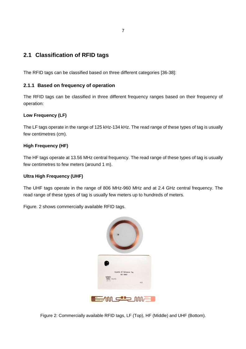
RFID is a wireless automatic identification technology that uses electromagnetic interaction to iden-
tify, sense and track people or objects with transponders i.e. tags [5]. The advantage this technology
offers over its predecessors (bar code reading) in identification is non-line of sight wireless detection.
Figure. 1 shows a basic RFID system. The system has three main parts: reader device, reader an-
tenna and tag. The whole system can be attached to a computer/server with an application that can
convert the data into human readable format. The RFID tag consists of a tag antenna and IC. The
IC stores the data in the memory and uses impedance modulation to establish communication be-
tween the reader and the tag. Typically, the IC has a specific wake up power which should be re-
ceived at the tag antenna so that the IC starts working. The performance of an RFID tag is normally
described by its read range i.e. the maximum distance between the reader and the tag at which the
tag can communicate and still be read with the reader [36,37].
Figure 1: RFID system.
Reader
RFID Tag
Reader Antenna
Server
2 Radio frequency identification technology
7
2.1 Classification of RFID tags
The RFID tags can be classified based on three different categories [36-38]:
2.1.1 Based on frequency of operation
The RFID tags can be classified in three different frequency ranges based on their frequency of
operation:
Low Frequency (LF)
The LF tags operate in the range of 125 kHz-134 kHz. The read range of these types of tag is usually
few centimetres (cm).
High Frequency (HF)
The HF tags operate at 13.56 MHz central frequency. The read range of these types of tag is usually
few centimetres to few meters (around 1 m).
Ultra High Frequency (UHF)
The UHF tags operate in the range of 806 MHz-960 MHz and at 2.4 GHz central frequency. The
read range of these types of tag is usually few meters up to hundreds of meters.
Figure. 2 shows commercially available RFID tags.
Figure 2: Commercially available RFID tags, LF (Top), HF (Middle) and UHF (Bottom).
8
2.1.2 Based on electromagnetic interaction
The RFID tags can be categorised into two types based on the electromagnetic interaction; Near-
field and far-field. The LF and HF RFID tags use near-field coupling while the UHF RFID tags use
far-field for communication. The near-field RFID tags have smaller read range due to the rapid de-
caying of energy however the far-field RFID tags have larger read ranges and smaller size.
2.1.3 Based on power supply for the tag
The RFID tags can be classified in three different categories based on the power supply of the tag:
Active RFID tags
The active RFID tags have their own power supply and do not rely on power supplied by the reader
antenna for communication. These types of RFID tags have large read ranges but the life span of
systems depends on the life span of the power source. The cost of active RFID is also higher in
comparison with other types due to the presence of the power supply.
Semi-passive RFID tags
The semi-passive RFID tags have a power supply to activate the IC but use reader antenna’s power
for communication. The read range of these tags is less than the active RFID tags.
Passive RFID tags
The passive RFID tags have no power supply and completely rely on the reader antenna’s power
for activating the IC as well as for data transmission. Passive RFID tags have a long life span and
do not need any maintenance or battery replacement. Due to this, passive RFID tags have low cost
and are abundantly used in the wireless sensing applications nowadays.
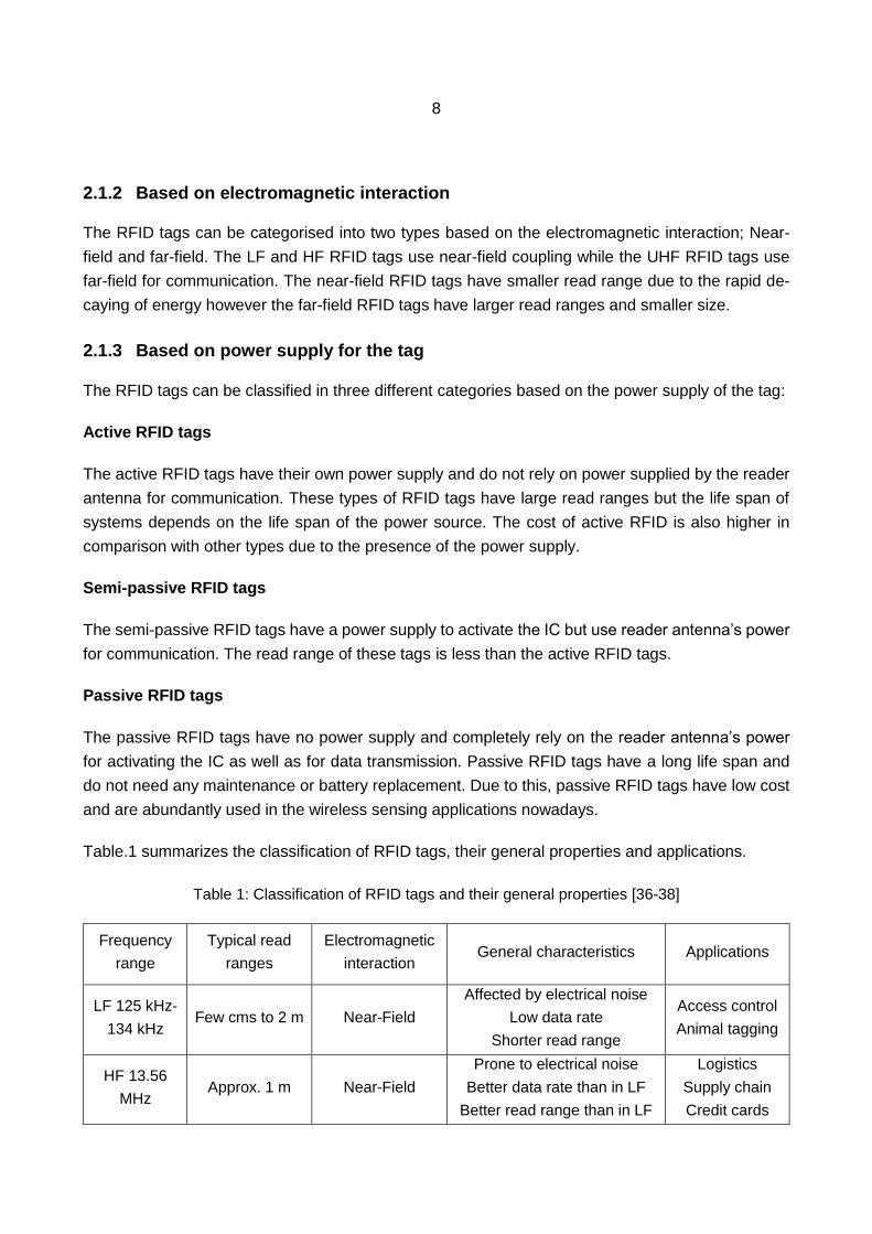
Table.1 summarizes the classification of RFID tags, their general properties and applications.
Table 1: Classification of RFID tags and their general properties [36-38]
Frequency
range
Typical read
ranges
Electromagnetic
interaction General characteristics Applications
LF 125 kHz-
134 kHz Few cms to 2 m Near-Field
Affected by electrical noise
Low data rate
Shorter read range
Access control
Animal tagging
HF 13.56
MHz Approx. 1 m Near-Field
Prone to electrical noise
Better data rate than in LF
Better read range than in LF
Logistics
Supply chain
Credit cards

9
UHF 806
MHz-960
MHz and 2.4
GHz
Few meters to
hundred meters
Typically 5 m
Far-Field
Smaller size
Low cost
Larger read range
High data rate
Supply chain
Parking access
control
Electronic toll
collection
The focus of this thesis is on the passive UHF RFID due to its advantages such as smaller size, low
cost, longer life span and larger read range distance.
2.2 Fundamental parameters of antennas
The antenna is the most essential component of a communication system. According to Webster’s
Dictionary, an antenna is defined as: “It is usually a metallic device (as a rod or wire) for transmitting
or receiving waves”. Antennas are passive components and are reciprocal devices i.e. its properties
remain the same whether it is used as a receiving or a transmitting device. Time-varying current or
an acceleration (or deceleration) of charges are two conditions that need to be met to produce time
varying E (Electric) and H (Magnetic) fields in the antenna. When these two conditions are met, the
antenna will radiate in all directions [39,40].
2.2.1 Radiation fields near an antenna
The radiation field near an antenna can be separated into three regions that are reactive near-field,
radiating near-field (Fresnel Zone) and far field (Fraunhofer Zone) [39]. The reactive near-field is
immediately near to the antenna where the reactive fields predominates. Generally, the reactive
near-field of the antenna is at a distance 𝑅 < 0.62√𝐷3
𝜆 from the antenna surface, where 𝜆 is the wave-
length and D is the largest dimension of the antenna. The radiating near-field or the Fresnel zone
lies in between the reactive near-field and the far-field region. In this field the angular field distribution
is dependent upon the distance from the antenna. The radiating near-field lies at a distance range
of 0.62√𝐷3
𝜆< 𝑅 <
2𝐷2
𝜆. As explained in the classification of RFID tags, the LF and the HF tags operate
in near-field region and due to the rapid decaying of fields, the read range of these tags are limited.
The most important field region is the far-field region where the radiation pattern does not change
shape with distance and a propagating wave can be assumed as a plane wave. The far-field region
start from 𝑅 >2𝐷2
𝜆 and expands away from the antenna.

10
2.2.2 Radiation pattern
The graphical representation of the field strength transmitted or received by the antenna is known
as radiation pattern [39]. The radiation pattern can be divided into two planes i.e. E-plane and H-
plane. Both these planes have their corresponding E-plane and H-plane vectors. The radiation pat-
tern is usually defined in the far-field region of the antenna because the field distribution is independ-
ent of the distance from the antenna. Based on the pattern of radiation we can classify antennas into
three types: isotropic, omni-directional and directional radiation patterns. An isotropic antenna radi-
ate fields equally in all directions. This type of radiator is considered the ideal case. The omni-direc-
tional antenna radiate fields in a specific plane however, a directional antenna radiate fields in a
specific direction. The radiation pattern is generally described in decibels (dB) scales.
2.2.3 Directivity, efficiency and gain
The directivity of an antenna is the ration of radiation intensity in a specific direction to the average
radiation intensity (Eq. 1). The radiation intensity U(θ,ϕ) is the power radiated in a given direction per
unit solid angle, measured in watts per steradians or square radians [41].
𝐷 (𝜃, 𝜙) = 𝑈 (𝜃,𝜙)
𝑈𝑎𝑣 =
𝑈 (𝜃,𝜙)1
4𝜋∫ ∫ 𝑈 (𝜃,𝜙) 𝑠𝑖𝑛𝜃 𝑑𝜃 𝑑𝜙
𝜋0
2𝜋0
. (1)
The antenna directivity is a dimension less quantity and its value ranges from unity (for isotropic
antenna) to greater than unity (for non-isotropic antennas). The directivity is generally expressed in
dBi i.e. the directivity of the antenna under test over the directivity of an isotropic antenna.
The efficiency of the antenna, considered to be loss less (Input power is equal to radiated power), is
1, however practically this is not possible. Some of the power is lost in ohmic and other losses i.e.
Pohmic. The efficiency of the antenna can be expressed as Eq. 2 [41]:
𝑒𝑐𝑑 = 𝑃𝑟𝑎𝑑
𝑃𝑖𝑛=
𝑃𝑟𝑎𝑑
𝑃𝑟𝑎𝑑+ 𝑃𝑜ℎ𝑚𝑖𝑐 . (2)
Another important loss is due to the mismatch between the antenna input terminals and the antenna
feed line. This is known as reflection or mismatch efficiency er. Hence, the total efficiency of the
antenna can be expressed as,
𝑒𝑡𝑜𝑡𝑎𝑙 = 𝑒𝑐𝑑 𝑒𝑟 . (3)
Gain or power gain shows how efficiently the available power at the input terminals of the antenna
is transmitted. The unit of gain is dB; if taken considering the isotropic antenna then it is represented
in dBi. Gain and directivity are related to each other by the efficiency of the antenna as [39] [41],
𝐺 = 𝑒𝑡𝑜𝑡𝑎𝑙 𝐷 (𝜃, 𝜙) . (4)

11
2.2.4 Input impedance
The input impedance is the impedance at the input terminals of an antenna which is written as:
𝑍𝐴 = 𝑅𝐴 + 𝑗𝑋𝐴 . (5)
where, real part of the impedance represents power that is either radiated away or absorbed within
the antenna while the imaginary part represents the power that is stored in the near field of the
antenna. The real part RA is a combination of radiation resistance Rr and loss resistance RL. The
radiation resistance Rr represents the radiated power and loss resistance RL represents the power
dissipated as heat [39] [41].
2.3 Performance metrics in passive UHF RFID tags
2.3.1 Impedance matching
To have an efficient power transfer between the IC and RFID tag antenna, a proper impedance
matching needs to be assured. Figure. 3 shows the equivalent circuit model of a passive RFID tag
with IC.
Figure 3: Equivalent circuit of passive RFID tag.
The circuit shows two complex impedances ZA and ZIC which should be matched in order to transfer
maximum power and enable the best possible operation. From the circuit, current and power reflec-
tion coefficient can be express as,
𝐼 =𝑉𝐴
𝑍𝐴+𝑍𝐼𝐶 . (6)
𝛤 =𝑍𝐼𝐶− 𝑍𝐴
∗
𝑍𝐼𝐶+ 𝑍𝐴 . (7)

12
Γ is the power reflection coefficient which represents the mismatch between the antenna and the IC
impedances [42]. An alternate way is to express it as the power transmission coefficient [43].
𝜏 = 1 − |𝛤|2 where 0 ≤ τ ≤ 1. (8)
The tag IC has nonlinear input power and frequency dependent input impedance which is capacitive
thus to have a perfect matching and maximum power transfer, the input reactance of the tag antenna
input impedance should be inductive [44]. In reality, commonly used tag antennas such as small
dipoles have capacitive input reactance [39]. This implies a need for transforming the input imped-
ance of the antenna to inductive. This is achieved by using a matching network between the IC and
the RFID tag antenna [45,46].
2.3.2 Read range
The maximum distance at which the information stored in the RFID tag IC can successfully be read
by the reader is known as the read range [5]. It is the most important performance indicator of an
RFID tag. Usually from an RFID tag designer perspective, the impedance matching, the IC wake up
power and the realized gain are the three important factors that can increase the read range.
2.3.3 Threshold power
The transmission power required to wake up the IC is known as threshold power [5]. A low threshold
power will allow longer read ranges. The threshold power of a tag can be expressed using the Friis
transmission equation:
𝑃𝑇𝑆 =𝑃𝐼𝐶
𝐺𝑡𝑥𝐺𝑡𝑎𝑔𝜏(𝜆
4𝜋𝑑)
2|𝑝𝑡𝑥.𝑝𝑡𝑎𝑔|
2 . (9)
where PIC is the wake up power of the IC, Gtx and Gtag are the gains of reader antenna and tag
antenna. 𝜆 is the wavelength, 𝜏 is the power transmission coefficient. d is the distance between the
reader and the tag. 𝑡𝑥 and 𝑡𝑎𝑔 are the unit electric field vectors of both the antennas.
The system will work when the power received on tag (Ptag) will be equal to the wake up power of
the IC (PIC). The equation can be written as [39] [47,48],
𝑃𝑡𝑎𝑔 = 𝑃𝑡𝑥𝐺𝑡𝑥𝐺𝑡𝑎𝑔 (𝜆
4𝜋𝑑)
2
. (10)
where Ptag is the power received on the tag and Ptx is the power transmitted by the reader antenna.
This implies that the theoretical read range to be:
𝑑𝑡𝑎𝑔 =𝜆
4𝜋√
𝑃𝑡𝑥𝐺𝑡𝑥𝐺𝑡𝑎𝑔𝜏
𝑃𝑇𝑆 . (11)

13
2.4 Integrated circuit
An RFID tag has two main parts: a tag antenna and an IC. The IC contains a memory unit which
stores the information. This memory is read and write both and can be used to identify a specific
object on which the RFID tag is placed. In this study NXP UCODE G2iL series IC is used [49]. The
chip has a wake up power of 15.8 µW (-18 dBm), 128 bit Electronic Product Code (EPC) memory
and 64-bit Tag IDentifier (TID) including 32-bit factory locked unique serial number. Figure. 4 shows
the NXP UCODE G2iL series IC. As seen in Figure. 4 the IC has 2 3x3 mm2 pads for attachment.
The IC has an equivalent input parallel resistance and capacitance of 2.85 kΩ and 0.91 pF respec-
tively [50]. In this study, we used Circuit Works conductive Ag epoxy CW2400 to attach the IC to the
RFID tags. The attachment is done by hand and after the attachment, the interconnection is sintered
for 10 minutes at 70 °C in the oven. If an oven is not available then the interconnection is left for four
hours to dry at room temperature.
Figure 4: NXP UCODE G2iL series IC used in the RFID study.
2.5 RFID measurement system
In this study, Voyantic Tagformance lite UHF RFID measurements system is used for the wireless
measurements of the fabricated tags, shown in Figure. 5. The system has a small anechoic chamber
(120 × 80 × 80 cm3), as shown in Figure. 6, in which the tag can be placed for the measurements.
The antenna of the RFID reader is linearly polarised patch antenna with the gain of 8 dB and oper-
ates between 800-1000 MHz. The output of reader ranges from 0 to 27 decibel milliwatts (dBm) and
the Radio Frequency (RF) receiver has sensitivity of -75 dBm.

14
Figure 5: Voyantic Tagformance lite.
Figure 6: Inside the Voyantic measurement unit.
The system uses the measured threshold power and the measured forward losses for calculating
the theoretical read range of a tag [51]. The system is first calibrated using a reference tag which
calculates the forward losses. The calibration is the most important step in which the reference tag
should be placed at the same location inside anechoic chamber which the tag under study would be
placed afterward for the measurements. The system calculates the power required to activate the
reference tag and then calculates the path loss which includes polarization losses, cable losses,
reader antenna gain and losses. Apart from threshold power measurements, the system can also
measure the radiation pattern of the tags at a certain frequency.

15
When comparing the Tagformance measurement system with the earlier theory explain in section
2.3.3 and in equation 9-11, the system measures the threshold power PTS by increasing the trans-
mitted power until the tag responds to the query made by the reader. This is effected by the wake
up power of the IC. The forward loss from the transmit port to the tag is calculated using a reference
tag during the calibration of the Tagformance measurement system. The theoretical read range
measured is thus limited by the maximal allowed transmitted power and can be calculated as:
𝑑𝑡𝑎𝑔 =𝜆
4𝜋√
𝐸𝐼𝑅𝑃
𝑃𝑇𝑆𝐿𝑓𝑤𝑑 . (12)
where 𝜆 is the wavelength, EIRP is the effective isotropic radiated power which is the maximum
isotropic radiated power allowed by the regulations i.e. 3.28 W in Europe and 4 W in US. EIRP can
be expressed as a product of transmitted power Ptx and the gain of the transmitting antenna Gtx. Lfwd
is the quantity which represents measured forward losses.
In this study, the Tagformance measurement system is used for the theoretical read range meas-
urement after the fabrication of the tags and is referred to as measured theoretical read range to
differentiate it from the simulated theoretical read range. Also, it is called measured theoretical read
range because it is not actually measured but calculated based on threshold power of the tag and
the reference tag that are actually measured.

16
This chapter explains different manufacturing methods for the fabrication of the antenna including
both the conductive trace and the substrate part. For the conductive part, the methods used are
inkjet printing, thermal printing, 3D dispensing and brush painting, whereas, for the substrate part,
3D printing is used. Post-processing methods are also explained at the end of the chapter along with
the antenna designs that are used in Publications I-VII.
3.1 Additive manufacturing
AM is a process in which a material is deposited layer-by-layer to make a design. In particular to the
manufacturing of the antennas, this technology is used to either deposit the conductive material on
the substrates or to make new substrates [52]. The AM technology is also termed as Rapid Proto-
typing. The process is quick, accurate and wastes less amount of material (mostly conductive mate-
rial) which makes it more suitable for the manufacturing of the antennas where conductive materials
are expensive. Nearly all of the AM machines have a software that can be used to optimize the
design and have an accuracy level of micro meters. The machines can deposit a wide range of
materials including nano-particle conductive inks, screen printable inks and plastics. At the end of
the AM process, the deposited material might require a post-processing.
3.1.1 Direct write (DW) technologies
The direct write technologies can create two dimensional (2D) and 3D structures on flat, flexible or
conformal surfaces in simple or complex geometry. Instead of using a mask for making the structure,
the DW has a computer generated design file which the software of the machine can optimize and
print accordingly [52-54]. The main application of DW includes printable electronics such as printing
antennas, passive components and batteries. DW has five categories: ink-based, thermal spray,
laser-transfer, beam deposition, liquid-phase, and beam tracing processes [52].
3 Antenna manufacturing methods

17
Ink-based DW technology
The ink-based DW is widely used in manufacturing due to its simplicity and cost-effectiveness. The
inks, containing the desired material, are deposited on the surface using a machine. These inks are
composed of the solvent and a certain percentage of desired material. After deposition, post-pro-
cessing is carried out to convert the ink into material having desirable properties e.g. high conduc-
tivity. Out of all the ink types, nano-particle inks are the most used nowadays. Ink-based DW can be
done by either depositing ink in drops with a print head or extruding continuously as a filament [52,53].
Figure. 7 shows both the deposition methods.
(a) (b)
Figure 7: Inkjet based direct writing techniques: (a) Jetting droplets (b) Continuous flow [52].
3.1.1.1 Inkjet printing
Inkjet printing has been used to manufacture antennas on versatile substrates such as paper, wood
and cardboards. The main advantage is highly accurate printing with a wide range of print resolution.
It is a contactless printing method i.e. the print head does not come into contact with the substrate
on which it is printing [55]. Each printer consists of a computer aided software which can make as
well as optimize a design. The inkjet printers are capable of depositing ink in drops (Drop on Demand)
or Continuously Stream (CS) through a print head. The CS is a simple process however the DOD is
complex and more effective. The printers capable of DOD mode utilize a pressure pulse or jetting
pulse for the drop formation [52]. The shape and size of drops depend on the jetting pulse shape.
The actuator is responsible for forming these pulses. Figure. 8 shows the drop formation in DOD
inkjet printers.
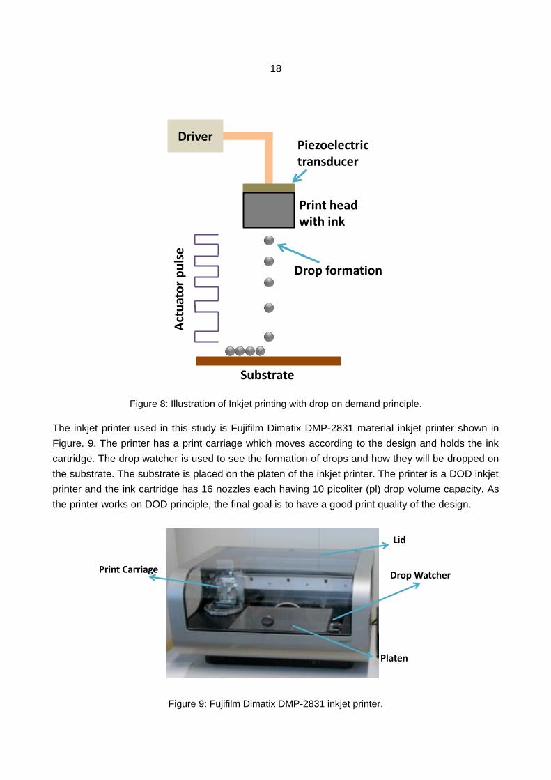
18
Figure 8: Illustration of Inkjet printing with drop on demand principle.
The inkjet printer used in this study is Fujifilm Dimatix DMP-2831 material inkjet printer shown in
Figure. 9. The printer has a print carriage which moves according to the design and holds the ink
cartridge. The drop watcher is used to see the formation of drops and how they will be dropped on
the substrate. The substrate is placed on the platen of the inkjet printer. The printer is a DOD inkjet
printer and the ink cartridge has 16 nozzles each having 10 picoliter (pl) drop volume capacity. As
the printer works on DOD principle, the final goal is to have a good print quality of the design.
Figure 9: Fujifilm Dimatix DMP-2831 inkjet printer.
Act
uat
or
pu
lse
Print headwith ink
Piezoelectrictransducer
Drop formation
Substrate
Driver
Lid
Print CarriageDrop Watcher
Platen

19
The print quality is effected by several parameters which include jetting pulse shape, the temperature
of the platen and the ink cartridge, the number of nozzles used and the pattern resolution [52] [55].
Jetting pulse shape
Drop formation is the most important part of the printing process in inkjet printing. The jetting pulse
shape or waveform determines the drop formation. A voltage pulse is applied to the piezo-electric
transducer for each drop that ejects from the nozzle of the printer. A typical jetting pulse waveform
can be seen in Figure. 10.
Figure 10: Jetting pulse waveform of inkjet printer.
The pulse width and the amplitude have effects on the drop velocity. For a particular pulse width, the
increase in pulse voltage increases the drop velocity which means that increase in pulse voltage will
increase the drop formation and hence more ink will drop in the width. The jetting frequency also has
similar effect where the increase in frequency increases the drop velocity and size of the drop. The
jetting voltage ranges from 0-40 Volts (V).
Temperature of the platen and the ink cartridge
The temperature of the platen and ink have huge impact on the final print quality. The platen tem-
perature can be adjusted up to 60 °C. It determines how quickly the ink drop dries on the substrate.
The ink cartridge temperature effects the flow of the ink and varies from 28 to 70 °C. A higher tem-
perature will allow the ink to flow more and thus a low pulse voltage will be required for the drop
formation.

20
Number of nozzles
The Fujifilm Dimatix DMP-2831 print head of the ink cartridge have 16 nozzles. Before starting the
printing, the user can select the number of nozzles and the particular number of nozzle to be used
for printing. Increasing the number of nozzles decreases the time taken to complete a print.
Pattern resolution
The pattern resolution or print resolution is determined by the drop spacing. The drop spacing is the
distance between two drops from center to center. For example, if the drop spacing is 50 microns
then the distance between two adjacent drops in X-axis and Y-axis will be 50 microns apart from the
center. The cartridge mounting angle plays an important role in getting the same resolution in both
directions. The pattern resolution varies from 100 DPI (Drops per inches) to 5080 DPI.
The inkjet printable inks have low viscosity so that they can easily flow and the drop formation pro-
cess can be efficient. Although with benefits such as high accuracy and more control on lots of
printing parameters, the inkjet printing is a slow printing method and the amount of ink coming out of
the nozzle makes a very thin layer on the substrate. The speed of printing can be increased to some
extend by optimizing the jetting waveform or by using multiple nozzles at the same time while the
thin layer can be increased by depositing multiple layers instead of single to have a thick pattern on
the substrate [56,57].
3.1.1.2 3D dispensing
3D dispensing is a type of continuous nozzle dispensing process [58,59]. A smart pump is used to
push the ink towards the nozzle. The size of nozzle determines the amount of ink as well as the
accuracy of the pattern. The 3D dispensing does not require a mask and have a computer aided
software for optimizing the design. NScrypt tabletop series 3D direct write dispensing system shown
in Figure. 11 is used in this study for the antenna manufacturing.
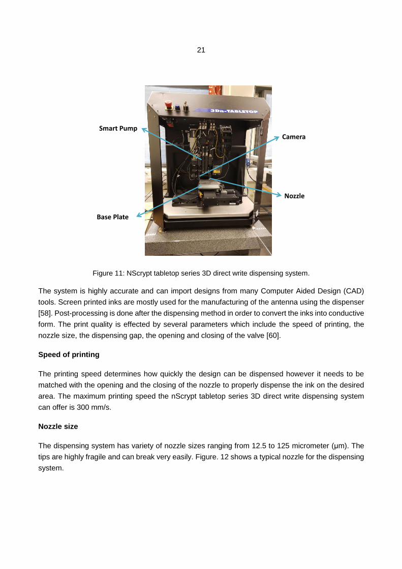
21
Figure 11: NScrypt tabletop series 3D direct write dispensing system.
The system is highly accurate and can import designs from many Computer Aided Design (CAD)
tools. Screen printed inks are mostly used for the manufacturing of the antenna using the dispenser
[58]. Post-processing is done after the dispensing method in order to convert the inks into conductive
form. The print quality is effected by several parameters which include the speed of printing, the
nozzle size, the dispensing gap, the opening and closing of the valve [60].
Speed of printing
The printing speed determines how quickly the design can be dispensed however it needs to be
matched with the opening and the closing of the nozzle to properly dispense the ink on the desired
area. The maximum printing speed the nScrypt tabletop series 3D direct write dispensing system
can offer is 300 mm/s.
Nozzle size
The dispensing system has variety of nozzle sizes ranging from 12.5 to 125 micrometer (μm). The
tips are highly fragile and can break very easily. Figure. 12 shows a typical nozzle for the dispensing
system.
CameraSmart Pump
Base Plate
Nozzle

22
Figure 12: Typical nozzle of Nscrypt 3D dispensing system.
Dispensing gap
The dispensing gap is the distance between the substrate surface and the nozzle tip. Figure. 13
illustrates how the ink is deposited on a substrate from pump “p”. If the gap is not set properly then
the ink can gather at some points to make the pattern non-uniform, also if the tip is too close to the
substrate then printing multiple layers can affect the final design.
Figure 13: Illustration of dispensing gap between nozzle and substrate.
Opening and closing of valve
Opening and closing of the valve determines the continuous flow of the ink. The valve should open
and close according to the design of the print. In the nScrypt 3D direct write dispensing system, the

23
software converts the design into a code format and then determines the opening and the closing of
the valve based on the distance covered by the valve during the printing.
3.1.2 Masking techniques
In the masking technique, a mask is required to make the exact design. The accuracy of the design
in the masking technique depends on the mask. The most simple, quick and cost-effective masking
technique is brush painting.
3.1.2.1 Brush painting
In the brush painting method, the antenna is manufacturing by dipping the brush in the ink or paste
and applying it directly on the substrate [61]. The method is quick however it doesn’t offer high ac-
curacy. As it is done by hand, the amount of ink or paste can never be the same whenever the brush
is dipped. Usually, a single layer of brush painting is enough to form a thick material surface ranging
from 10 μm to 40 μm. Depending on the ink or paste, the brush painting method also requires a post-
processing. An illustration of the brush painting method can be seen in Figure. 14.
Figure 14: Illustration of brush painting method.
3.1.3 Thermal transfer print (TTP)
Thermal transfer printing is the principle on which thermal printer works [26] [62]. A multi-layer ribbon
having thin layer of metal and heat-sensitive acrylic adhesive is installed in the thermal printer. The
metal is transferred to the substrate using a thermal print-head which selectively activate the desired
regions. Although the method is quick and accurate but there is a chance of wastage of metal. Figure.
15 shows the schematics of thermal printing method.
SubstrateMaskBrush with paste

24
Figure 15: Schematics of thermal printing method.
In this study, Zebra S4M thermal printer is used [63]. The printer has a print-head resolution of 300
DPI and can print at a speed of 5 cm/s. The design can be loaded into the printer using a USB
interface. The printing method doesn’t require any post-processing and the printed designs are ready
to be used immediately. The printer is capable of multi-layer printing but depends highly on the ad-
hesion between the metal and heat-sensitive layer, and the alignment during the multi-layer printing.
Figure. 16 and 17 show the Zebra S4M thermal printer and its schematics.
Figure 16: Zebra S4M thermal printer.
Controls
Printed Tags
ConductiveRibbon
Paper

25
Figure 17: Schematics of Zebra S4M thermal printer.
3.1.4 3D printing
3D printing is the latest manufacturing technology which has gained a lot of interest in research fields
including wireless electronics industry. 3D printing can be used to manufacture complex 3D designs
by using layer-by-layer deposition of different materials [52] [64]. It is usually used for making sub-
strates as well as conductive designs for antenna applications. The main advantage it offers is cus-
tomizable structures (shape, size, infill and thickness), electrical properties (dielectric permittivity and
loss tangent) and mechanical properties (stretchability, flexibility, weight). Acrylonitrile Butadiene
Styrene (ABS) and PolyLactic Acid (PLA) are the most commonly used 3D printable materials [65-
67]. Both of these materials are non-flexible however nowadays flexible material such as NinjaFlex
is also available for 3D printing. Although there are different types of 3D printers but the most com-
monly used ones are Fused Deposition Modelling (FDM). Prior to the printing process, the 3D CAD
design should be sliced in layers using a 3D printer software or a slicer tool. Figure. 18 shows a
simple rectangular patch of 1.2 mm thickness sliced in 6 layers of 0.2 mm each using a slicer tool.
(a) (b)
Figure 18: Spliced rectangular patch (a) Substrate with boundary (b) Side view showing sliced layers.
26
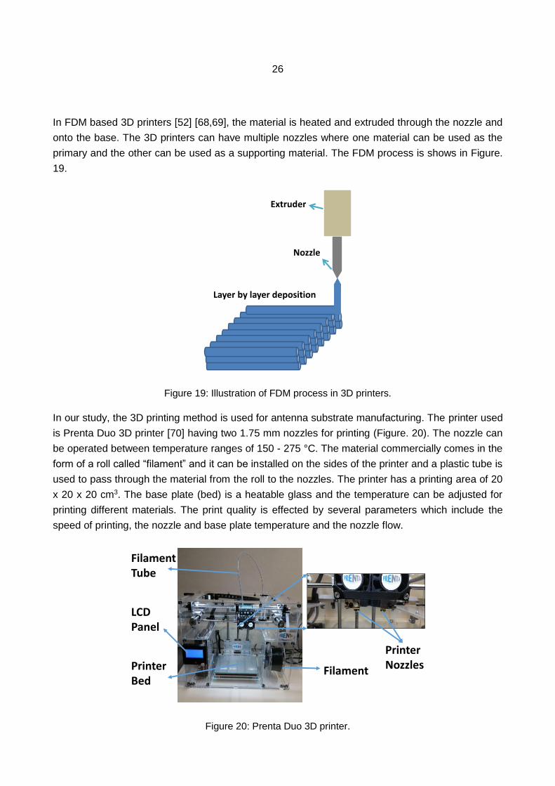
In FDM based 3D printers [52] [68,69], the material is heated and extruded through the nozzle and
onto the base. The 3D printers can have multiple nozzles where one material can be used as the
primary and the other can be used as a supporting material. The FDM process is shows in Figure.
19.
Figure 19: Illustration of FDM process in 3D printers.
In our study, the 3D printing method is used for antenna substrate manufacturing. The printer used
is Prenta Duo 3D printer [70] having two 1.75 mm nozzles for printing (Figure. 20). The nozzle can
be operated between temperature ranges of 150 - 275 °C. The material commercially comes in the
form of a roll called “filament” and it can be installed on the sides of the printer and a plastic tube is
used to pass through the material from the roll to the nozzles. The printer has a printing area of 20
x 20 x 20 cm3. The base plate (bed) is a heatable glass and the temperature can be adjusted for
printing different materials. The print quality is effected by several parameters which include the
speed of printing, the nozzle and base plate temperature and the nozzle flow.
Figure 20: Prenta Duo 3D printer.
Nozzle
Layer by layer deposition
Extruder
PrinterNozzlesFilamentPrinter
Bed
LCD Panel
FilamentTube

27
3.1.5 Embroidery
Embroidery machines have recently been used for the manufacturing of the antennas [71-73]. It is a
good alternative to conductive inks as embroidery utilizes conductive threads. The process is simple,
quick and CADs can be easily loaded in the embroidery machines. The substrate fits in the hoop
and the embroidery process is done by selecting the design and the stitch types. In this study, the
embroidery process is done using Husqvarna Viking embroidery [74] machine shown in Figure. 21.
Figure 21: Husqvarna Viking embroidery machine.
3.2 Substrates and conductive materials
3.2.1 Inkjet and thermal printing
The study related to inkjet and thermal printing is done using polyimide substrate (Kapton HN, re-
ferred as Kapton or KP) and novel polyester based substrate material (Flexcon THERMLfilm Select
21944E (TC-390), referred as THERMLfilm or TF). Thickness of Kapton and THERMLfilm is 50 µm
and 70 µm, and relative permittivities are 3.2 and 3.0 respectively.
For thermal printing, 260 nm thick Al and 340 nm thick Cu film MetallographTM Conductive Thermal
Transfer Ribbons (CTTR) are used as conductor. For inkjet printing, Harima’s NPS-JL Ag and ANI
Cu-IJ70 Cu nano-particle inks are used. The reason for using Ag and Cu ink is that they are the most
widely used nano-particle inks for inkjet printing. The Ag nano-particle ink is expensive but it is easy
to post-process using thermal curing at adequate temperatures (100 to 150 °C). On the other hand,
Cu nano-particle ink is more conductive and less expensive compared with Ag nano-particle ink but
it easily oxidizes in ambient environment resulting in an insulator (Copper oxide).
Embroidery Arm
Bobbin CoverNeedle and PresserFoot
Square Hoop (120 x 120)
LCD Panel

28
3.2.2 3D printing
3D printing, in this study, is utilized for making the flexible substrates using NinjaFlex material from
Ninjatek. The material has a 200 mm reel diameter and 1.75 mm thread diameter. A single filament
costs 50 € and contains approx. 173 meters of material. During the printing process, a single sub-
strate sample utilizes around 1500-2000 mm Ninjaflex material, which means it can print up to 90
substrate samples with one filament making it cost-effective in terms of manufacturing. For the con-
ductive part 3D dispensing and embroidery is used. In 3D dispensing screen printable stretchable
Ag conductive paste (DuPont PE872) and in embroidery multifilament Ag plated thread (Shieldex
multifilament thread 110f34 dtex 2-ply HC) [75] is used.
3.3 Post-processing
Most of the inks require post-processing before their properties can be modified or improved for
using as conductive part of the antenna [52]. The selection of the post-processing method depends
on the type of the ink.
3.3.1 Thermal curing
Thermal curing is the most commonly used post-processing method. A conventional oven is used to
provide enough temperature for the printed sample so that the organic solvents are removed and
conductive particles can stick together and form a conductive surface. The temperature value is set
according to the ink and the type of the substrate. If, the ink requires higher temperature but the
substrate cannot withstand it then thermal sintering is not used e.g. the Ag nano-particle ink used in
our study can be thermally cured however the Cu nano-particle ink required higher reducing temper-
ature and photonic sintering is preferred. The main drawbacks of thermal curing are that it is a slow
process and the whole design is exposed to the heating process.
3.3.2 Photonic sintering
Photonic sintering uses high energy pulse light to sinter the conductive material [76]. It is also known
as intense pulsed light sintering (IPL). The process is quick and can be applied to selective areas of
the printed pattern by adjusting the gap between the mask. Typically photonic sintering systems use
Xenon flash lamps for omitting the energy, mask for adjusting the exposure of light to the sample
and reflector for focusing the light. A simple photonic sintering system is illustrated in Figure. 22.

29
Figure 22: Illustration of a simple photonic sintering system.
The photonic sintering system used in this study is Xenon Sinteron 2010-L system [77]. The specifi-
cations of the machine are listed in Table. 2.
Table 2: General properties of Xenon Sinteron 2010-L system
Parameter Specifications
Lamp LH-840 Lamp Housing
Pulsed Duration in seconds (s) 100 μs - 2000 μs in increments of 5 μs
Pulse Rate in Hertz (Hz) 1 Hz - 10 Hz in increments of .001 Hz
Pulse Voltage in Volts (V) 1800 V - 3100 V
Pulse Energy in Joules (J) 27 J - 2000 J
Pulse count in numbers 1 - 2000
Aperture ratio 10 mm - 80 mm
Distance between light source and sample 25 mm - 76 mm
Modes Single, double, continuous and burst
Figure. 23 shows the Sinteron 2010-L rack along with the lamp housing and the sample placing
space. The sinteron rack has a power supply, high voltage capacitors and a controller system while
the lamp housing, the xenon flash lamp and the cooling system are together on the conveyor table.
Mask
Table
Lamp and Reflector
Lamp Flash
Printed sample
30
Figure 23: Sinteron 2010-L photonic sintering system.
The energy provided to the sample should be optimized as low energy will not sinter the sample and
high energy can damage the sample. Before explaining the energy calculations for the sinteron ma-
chine, it is good to understand the different operating modes.
Flash modes
The sinteron machine has four operating modes [77]. The details and the waveforms (Figure. 24-26)
are given below:
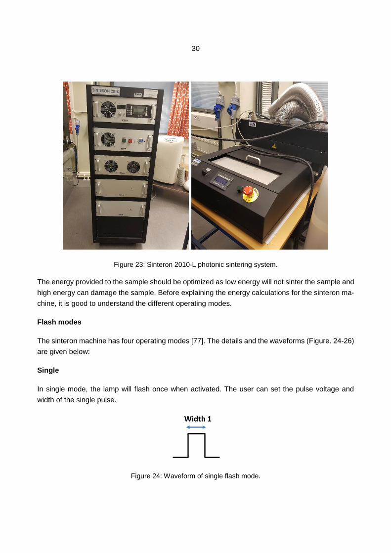
Single
In single mode, the lamp will flash once when activated. The user can set the pulse voltage and
width of the single pulse.
Figure 24: Waveform of single flash mode.
Width 1
Width 1 Width 2
Period
Period
Width 1
Period
Width 1
31
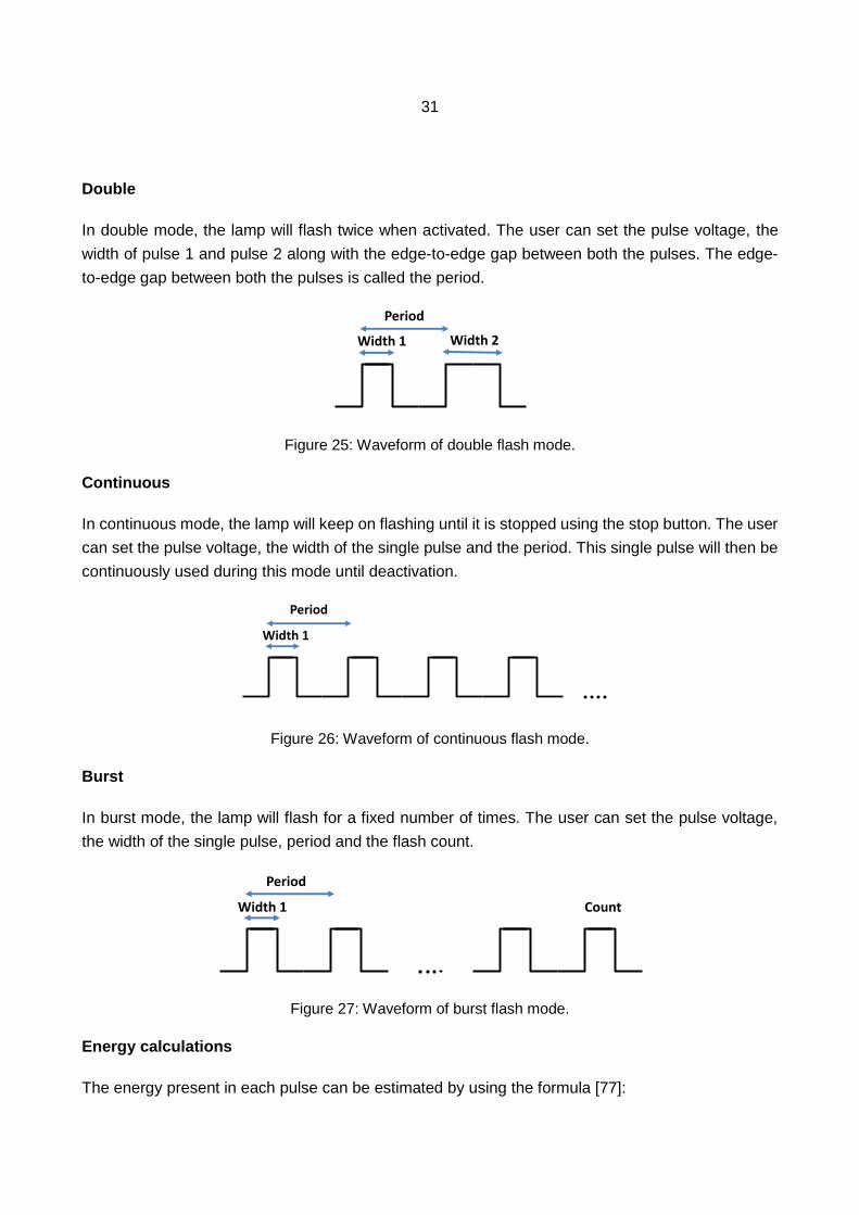
Double
In double mode, the lamp will flash twice when activated. The user can set the pulse voltage, the
width of pulse 1 and pulse 2 along with the edge-to-edge gap between both the pulses. The edge-
to-edge gap between both the pulses is called the period.
Figure 25: Waveform of double flash mode.
Continuous
In continuous mode, the lamp will keep on flashing until it is stopped using the stop button. The user
can set the pulse voltage, the width of the single pulse and the period. This single pulse will then be
continuously used during this mode until deactivation.
Figure 26: Waveform of continuous flash mode.
Burst
In burst mode, the lamp will flash for a fixed number of times. The user can set the pulse voltage,
the width of the single pulse, period and the flash count.
Figure 27: Waveform of burst flash mode.
Energy calculations
The energy present in each pulse can be estimated by using the formula [77]:
Width 1
Width 1 Width 2
Period
Period
Width 1
Period
Width 1
Width 1
Width 1 Width 2
Period
Period
Width 1
Period
Width 1
Width 1
Width 1 Width 2
Period
Period
Width 1
Period
Width 1 Count

32
𝐸 = (𝑉
3120)
2.4
× 𝑡 . (13)
where, E is the energy in joules, V the pulse voltage value in volts and t the time in microseconds.
3.4 Antenna designs
Three different RFID tag antennas are used for the RFID study [78-80] (Figure. 28-30) and one
simple rectangular patch is used for the wearable antenna study (Figure. 31). The purpose of using
three different RFID tag antenna designs, which have different structure with narrow and wide tracks,
allow an extensive study of printing methods. The design characteristics of three tags are provided
in detail in the previous RFID studies [78-80]. All the tag designs can achieve satisfied performance
in UHF band (860 MHz to 960 MHz).
Figure 28: Tag design 1: short dipole-type tag [78].
Figure 29: Tag design 2: wideband tag [79].
Figure 30: Tag design 3: straight dipole tag [80].
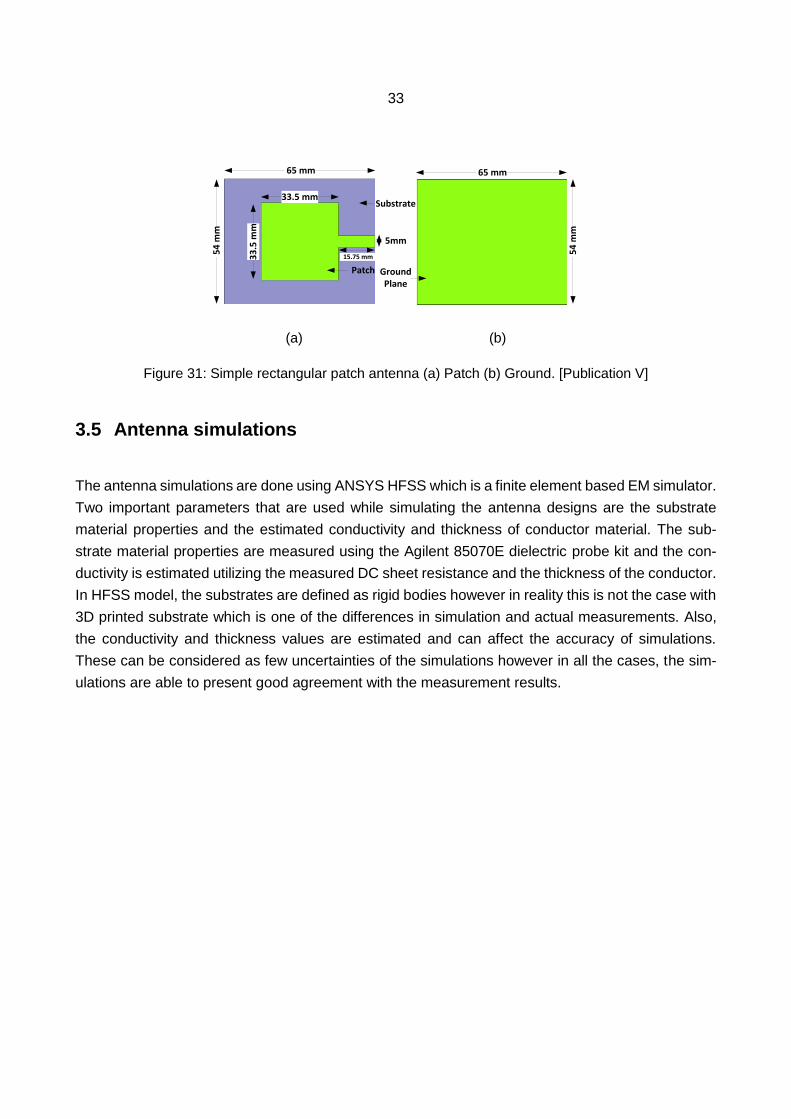
33
(a) (b)
Figure 31: Simple rectangular patch antenna (a) Patch (b) Ground. [Publication V]
3.5 Antenna simulations
The antenna simulations are done using ANSYS HFSS which is a finite element based EM simulator.
Two important parameters that are used while simulating the antenna designs are the substrate
material properties and the estimated conductivity and thickness of conductor material. The sub-
strate material properties are measured using the Agilent 85070E dielectric probe kit and the con-
ductivity is estimated utilizing the measured DC sheet resistance and the thickness of the conductor.
In HFSS model, the substrates are defined as rigid bodies however in reality this is not the case with
3D printed substrate which is one of the differences in simulation and actual measurements. Also,
the conductivity and thickness values are estimated and can affect the accuracy of simulations.
These can be considered as few uncertainties of the simulations however in all the cases, the sim-
ulations are able to present good agreement with the measurement results.
33.5 mm
33
.5 m
m
65 mm
54
mm
5mm
Substrate
Patch
65 mm
54
mm
(a) (b)
Ground Plane
15.75 mm

34
This chapter describes two manufacturing methods, the Inkjet and the thermal printing for the fabri-
cation of passive UHF RFID tags. Section 4.1 and 4.2 highlights the fabrication and reliability testing
of Ag based inkjet and Al based thermal printed tags. The work is presented from Publication I and
II. Section 4.3 explains the fabrication of Cu based inkjet and thermal printed tags from Publication
III and IV.
4.1 Inkjet and thermal transfer printed passive UHF RFID tags
In this study, the comparison of inkjet and thermal printing is done for the manufacturing of passive
UHF RFID tags on polyimide (Kapton) and polyester-based substrates (THERMLfilm). The key con-
siderations during the comparison are achieved theoretical read ranges, the ease of fabrication, the
flexibility of optimizable parameters and compatibility of different substrates with the printing methods.
For inkjet printing Ag nano-particle ink and for thermal printing Al Metallograph™ CTTR is used. Tag
design 1 and 2 are used for this study. Optimization is done for both the printers with each of the
substrates. The printed layer thickness is measured using Veeco Wyko NT1100 optical profiling
system. The method presented in [81] is used to approximate the sheet resistance and the final
achieved conductivities of the inkjet printed samples. For the inkjet printed samples, the final sheet
resistance on Kapton and THERMLfilm is calculated to be 56.25 mΩ and 146.12 mΩ. The single
layer inkjet printed Ag resulted in 1 µm thick conductor on Kapton and around 0.4 - 0.6 µm on
THERMLfilm. The sheet resistance and thickness are used to calculate the achieved conductivity of
Ag ink i.e. 1.7x10⁷ S/m. For thermal transfer printed samples, the conductivity 2.40x10⁷ S/m men-
tioned by the manufacturer is used. Figure. 32-35 show the printed samples along with microscopic
surface pictures.
4 Inkjet and thermal printed passive UHF RFID tags

35
(a) (b)
Figure 32: Thermal printed Tag design 1 on: (a) Kapton (Al) (b) THERMLfilm (Al).
(a) (b)
Figure 33: Microscopic view of Thermal printed Tag design 1 on: (a) Kapton (Al) (b) THERMLfilm (Al). [Publication I]
(a) (b)
Figure 34: Inkjet printed Tag design 1 on: (a) Kapton (Ag) (b) THERMLfilm (Ag).
(a) (b)
Figure 35: Microscopic view of Inkjet printed Tag design 1 on: (a) Kapton (Ag) (b) THERMLfilm (Ag). [Publication I]

36
Figure. 36 and 37 illustrate the simulated and the measured theoretical read range values of the
printed RFID tag 1 and tag 2. The peak read ranges of the printed tags are tabulated in Table. 3.
The results show that for a particular tag, e.g. Tag 1, similar read ranges for thermal printed tag on
different substrates (i.e. Kapton and THERMLfilm) but for the inkjet printed samples the read ranges
are quite different. This is because of the ink absorption in inkjet printing, as THERMLfilm is a paper
based substrate and absorbs ink. Thus having less conductor thickness and different read ranges.
Table. 3 summarizes the measured theoretical read ranges of the fabricated tags.
Figure 36: Theoretical read ranges of Tag design 1 on Kapton substrate (Ag for inkjet and Al for thermal printing). [Publication I]
Figure 37: Measured theoretical read ranges of Tag design 1 and 2 on THERMLfilm substrate (Ag for inkjet and Al for thermal printing). [Publication I]
800 820 840 860 880 900 920 940 960 980 10000
1
2
3
4
5
6
7
8
Frequency [MHz]
Theore
tical R
ead R
ange (
RR
) [m
]
Simulated RR of Inkjet Printed Tag1
Measured RR of Inkjet Printed Tag1
Simulated RR of Thermal Printed Tag1
Measured RR of Thermal Printed Tag1
800 820 840 860 880 900 920 940 960 980 10001
2
3
4
5
6
7
8
9
Frequency [MHz]
Theore
tical R
ead R
ange (
RR
) [m
]
Inkjet Printed Tag1 sample 1
Inkjet Printed Tag1 sample 2
Thermal Printed Tag1 sample 1
Thermal Printed Tag1 sample 2
Inkjet Printed Tag2 sample 1
Inkjet Printed Tag2 sample 2
Thermal Printed Tag2 sample 1
Thermal Printed Tag2 sample 2
Tag 2
Tag 1
37
Table 3: Measured theoretical read range. [Publication I]
Printing Method Substrate Material Measured Theoretical Read Range [m]
Tag 1 Tag 2
Thermal Printing Kapton
Al 4.5 Not Available
THERMLfilm 4.3 7.8
Inkjet Printing Kapton
Ag 5.8 8.7
THERMLfilm 4.2 8.0
In thermal transfer print, the most important aspect is the successful transfer of the conductor to the
substrate. This limits the type of substrates the thermal transfer print supports. This is very clear from
the experiment as we are not able to have a successful printing of Tag 2 on Kapton using thermal
transfer print. Even for Tag 1 multiple tries are done before a tag design was successfully printed
although the design still had some missing conductive parts. This is due to the poor adhesiveness
of thermal ribbon on Kapton as shown in Figure. 38.
Figure 38: Adhesion problem with thermal printing on Kapton. [Publication I]
4.2 Reliability of inkjet and thermal transfer printed passive UHF RFID tags in high humidity conditions
In this work, the reliability of Inkjet and thermal transfer printed passive UHF RFID tags is studied on
THERMLfilm substrates with Tag design 2. A regular textile glue (Gutermann Creativ HT2, referred
as Glue 1) and a normal superglue (Loctite Super Glue, referred as Glue 2) are used to protect the
IC during the humidity test. Two glues are used to mitigate the effects of glue type on the tag perfor-
mance. The tag performance is measured in different conditions i.e. after fabrication, after applying
coating, immediately after the test and then after drying for 24 hours.
As seen from the Figure. 39, both the glues have no effect on the read range of the inkjet printed tag
however, glue 1 shifts the peak read range frequency to lower values. The tag antenna impedance
and ohmic losses are affected during the test and thus a shift in frequency is observed immediately
after the test. After 24 hours, the performance returns to normal. These results are appropriate for
many wireless applications where humidity/moisture can be a concern.
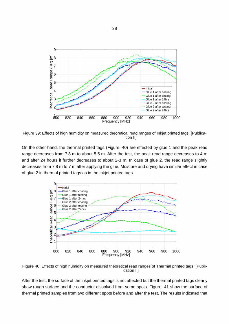
38
Figure 39: Effects of high humidity on measured theoretical read ranges of Inkjet printed tags. [Publica-tion II]
On the other hand, the thermal printed tags (Figure. 40) are effected by glue 1 and the peak read
range decreases from 7.8 m to about 5.5 m. After the test, the peak read range decreases to 4 m
and after 24 hours it further decreases to about 2-3 m. In case of glue 2, the read range slightly
decreases from 7.8 m to 7 m after applying the glue. Moisture and drying have similar effect in case
of glue 2 in thermal printed tags as in the inkjet printed tags.
Figure 40: Effects of high humidity on measured theoretical read ranges of Thermal printed tags. [Publi-cation II]
After the test, the surface of the inkjet printed tags is not affected but the thermal printed tags clearly
show rough surface and the conductor dissolved from some spots. Figure. 41 show the surface of
thermal printed samples from two different spots before and after the test. The results indicated that
800 820 840 860 880 900 920 940 960 980 10001
2
3
4
5
6
7
8
9
Frequency [MHz]
Theore
tical R
ead R
ange (
RR
) [m
]
Initial
Glue 1 after coating
Glue 1 after testing
Glue 1 after 24hrs
Glue 2 after coating
Glue 2 after testing
Glue 2 after 24hrs
800 820 840 860 880 900 920 940 960 980 1000
1
2
3
4
5
6
7
8
9
Frequency [MHz]
Theore
tical R
ead R
ange (
RR
) [m
]
Initial
Glue 1 after coating
Glue 1 after testing
Glue 1 after 24hrs
Glue 2 after coating
Glue 2 after testing
Glue 2 after 24hrs

39
the inkjet printed tags can withstand the high humidity conditions regardless of the glue used how-
ever in case of thermal printed tags the most important challenge is to find a suitable coating for the
tags to maintain their performance in high humidity conditions.
Figure 41: Surface of a Thermal printed antenna before and after test from two different parts. [Publica-tion II]
4.3 Cu based inkjet and thermal transfer printed passive UHF RFID tags
The performance of Cu based inkjet and thermal printed RFID tags are compared in Publication III
and IV with three different tag designs. Using Cu as conductive material reduces the cost of produc-
tion as Ag based inks are expensive. Previously, inkjet and screen printed Cu conductor is cured
using laser curing on different substrates [82]. The printing process remains the same as in previous
studies however in case of inkjet printing, the printed tags are post processed using photonic sinter-
ing.
For thermal printed Cu tags, a 340 nm thick Cu film is used. Figure. 42 and 43 show the printed
samples along with microscopic surface pictures and surface roughness. The Cu traces have an
RMS roughness of 19.8 nm whereas the Al traces have RMS roughness of 20.8 nm. Both the traces
have smoother surfaces when compared with inkjet Ag traces on THERMLfilm. The thermal printed
Cu antennas achieved conductivity of 3.9 × 10⁷ S/m. The conductivity measurement is explained in
detail in Publication III.

40
(a) (b)
Figure 42: Ready tag: (a) Thermal printed Cu tag (b) Microscopic picture of the surface. [Publication III].
Figure 43: Thermal printed Cu trace surface morphology. [Publication III]
The tag performance is evaluated through wireless tag measurements under the European RFID
transmission regulations as explained in Section 2.5. Figure. 44-46 show the read range of three
different thermal printed Cu tags compared with the tags fabricated in the previous studies (Al and
Ag based). For tag design 1, Thermal printed Cu antennas achieved maximum read range of 6.6 m
which is 2.2 m better than thermal printed Al antennas. This is due to the higher conductivity of Cu
traces and thick metallic layer. The thermal printed Cu antennas also managed to have a read range
improvement of 0.8 m over the inkjet printed antennas on Kapton and 1.7 m over the inkjet printed
antennas on THERMLfilm.
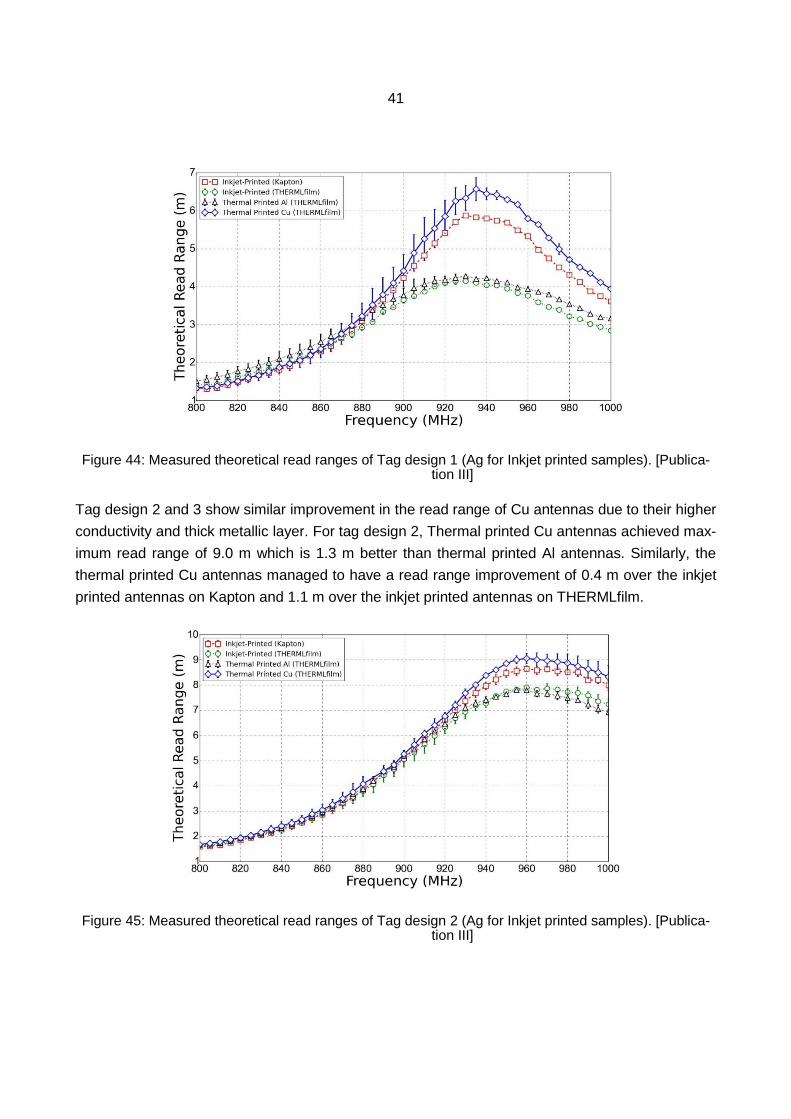
41
Figure 44: Measured theoretical read ranges of Tag design 1 (Ag for Inkjet printed samples). [Publica-tion III]
Tag design 2 and 3 show similar improvement in the read range of Cu antennas due to their higher
conductivity and thick metallic layer. For tag design 2, Thermal printed Cu antennas achieved max-
imum read range of 9.0 m which is 1.3 m better than thermal printed Al antennas. Similarly, the
thermal printed Cu antennas managed to have a read range improvement of 0.4 m over the inkjet
printed antennas on Kapton and 1.1 m over the inkjet printed antennas on THERMLfilm.
Figure 45: Measured theoretical read ranges of Tag design 2 (Ag for Inkjet printed samples). [Publica-tion III]
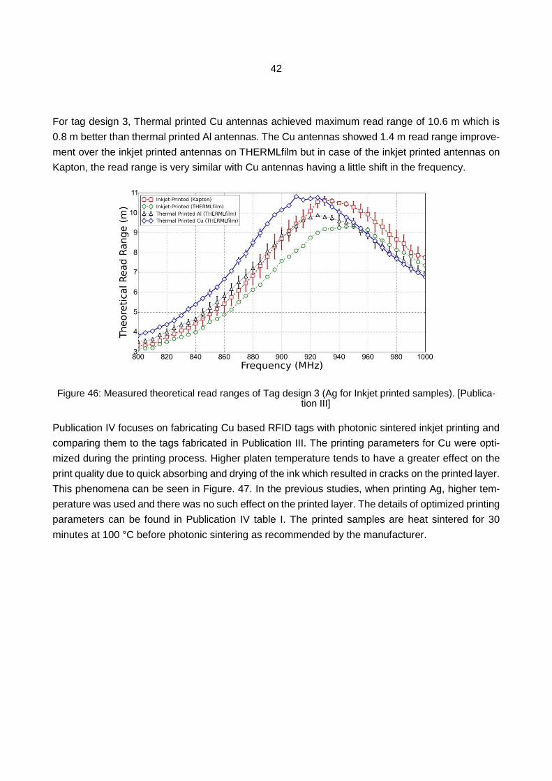
42
For tag design 3, Thermal printed Cu antennas achieved maximum read range of 10.6 m which is
0.8 m better than thermal printed Al antennas. The Cu antennas showed 1.4 m read range improve-
ment over the inkjet printed antennas on THERMLfilm but in case of the inkjet printed antennas on
Kapton, the read range is very similar with Cu antennas having a little shift in the frequency.
Figure 46: Measured theoretical read ranges of Tag design 3 (Ag for Inkjet printed samples). [Publica-tion III]
Publication IV focuses on fabricating Cu based RFID tags with photonic sintered inkjet printing and
comparing them to the tags fabricated in Publication III. The printing parameters for Cu were opti-
mized during the printing process. Higher platen temperature tends to have a greater effect on the
print quality due to quick absorbing and drying of the ink which resulted in cracks on the printed layer.
This phenomena can be seen in Figure. 47. In the previous studies, when printing Ag, higher tem-
perature was used and there was no such effect on the printed layer. The details of optimized printing
parameters can be found in Publication IV table I. The printed samples are heat sintered for 30
minutes at 100 °C before photonic sintering as recommended by the manufacturer.
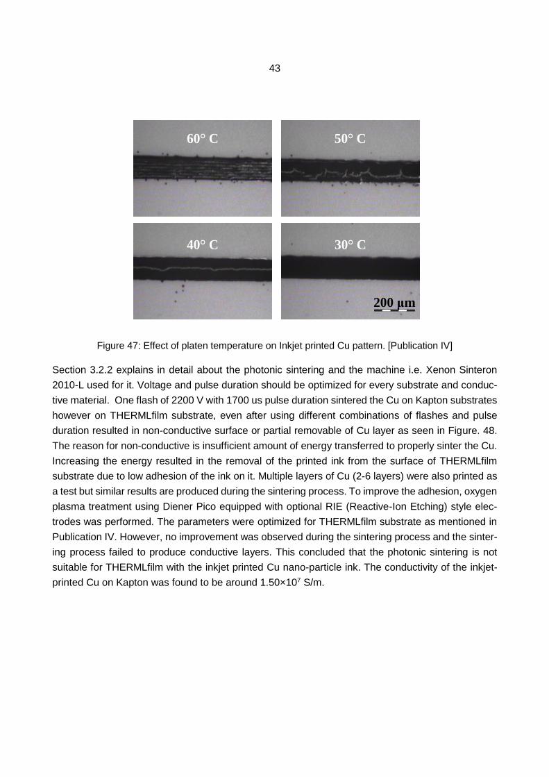
43
Figure 47: Effect of platen temperature on Inkjet printed Cu pattern. [Publication IV]
Section 3.2.2 explains in detail about the photonic sintering and the machine i.e. Xenon Sinteron
2010-L used for it. Voltage and pulse duration should be optimized for every substrate and conduc-
tive material. One flash of 2200 V with 1700 us pulse duration sintered the Cu on Kapton substrates
however on THERMLfilm substrate, even after using different combinations of flashes and pulse
duration resulted in non-conductive surface or partial removable of Cu layer as seen in Figure. 48.
The reason for non-conductive is insufficient amount of energy transferred to properly sinter the Cu.
Increasing the energy resulted in the removal of the printed ink from the surface of THERMLfilm
substrate due to low adhesion of the ink on it. Multiple layers of Cu (2-6 layers) were also printed as
a test but similar results are produced during the sintering process. To improve the adhesion, oxygen
plasma treatment using Diener Pico equipped with optional RIE (Reactive-Ion Etching) style elec-
trodes was performed. The parameters were optimized for THERMLfilm substrate as mentioned in
Publication IV. However, no improvement was observed during the sintering process and the sinter-
ing process failed to produce conductive layers. This concluded that the photonic sintering is not
suitable for THERMLfilm with the inkjet printed Cu nano-particle ink. The conductivity of the inkjet-
printed Cu on Kapton was found to be around 1.50×10⁷ S/m.
60 C
40 C
50 C
30 C
200 μm
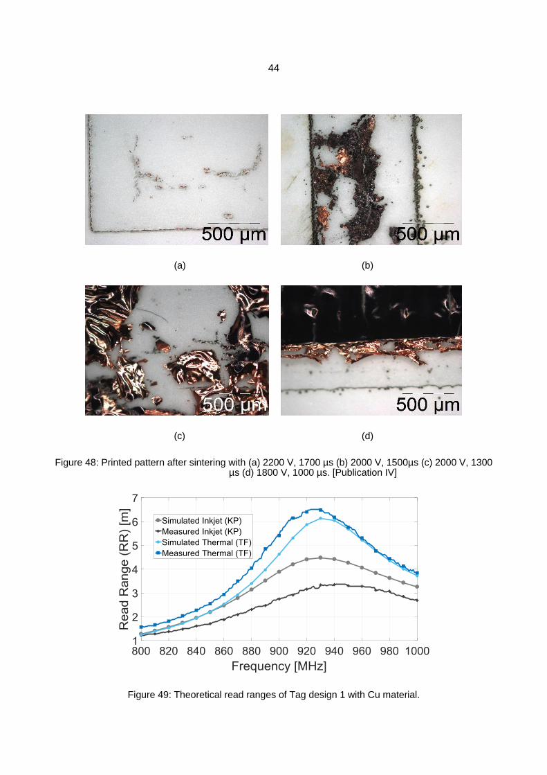
44
(a) (b)
(c) (d)
Figure 48: Printed pattern after sintering with (a) 2200 V, 1700 µs (b) 2000 V, 1500µs (c) 2000 V, 1300 µs (d) 1800 V, 1000 µs. [Publication IV]
Figure 49: Theoretical read ranges of Tag design 1 with Cu material.
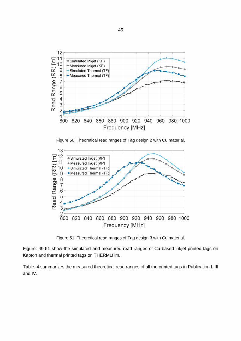
45
Figure 50: Theoretical read ranges of Tag design 2 with Cu material.
Figure 51: Theoretical read ranges of Tag design 3 with Cu material.
Figure. 49-51 show the simulated and measured read ranges of Cu based inkjet printed tags on
Kapton and thermal printed tags on THERMLfilm.
Table. 4 summarizes the measured theoretical read ranges of all the printed tags in Publication I, III
and IV.
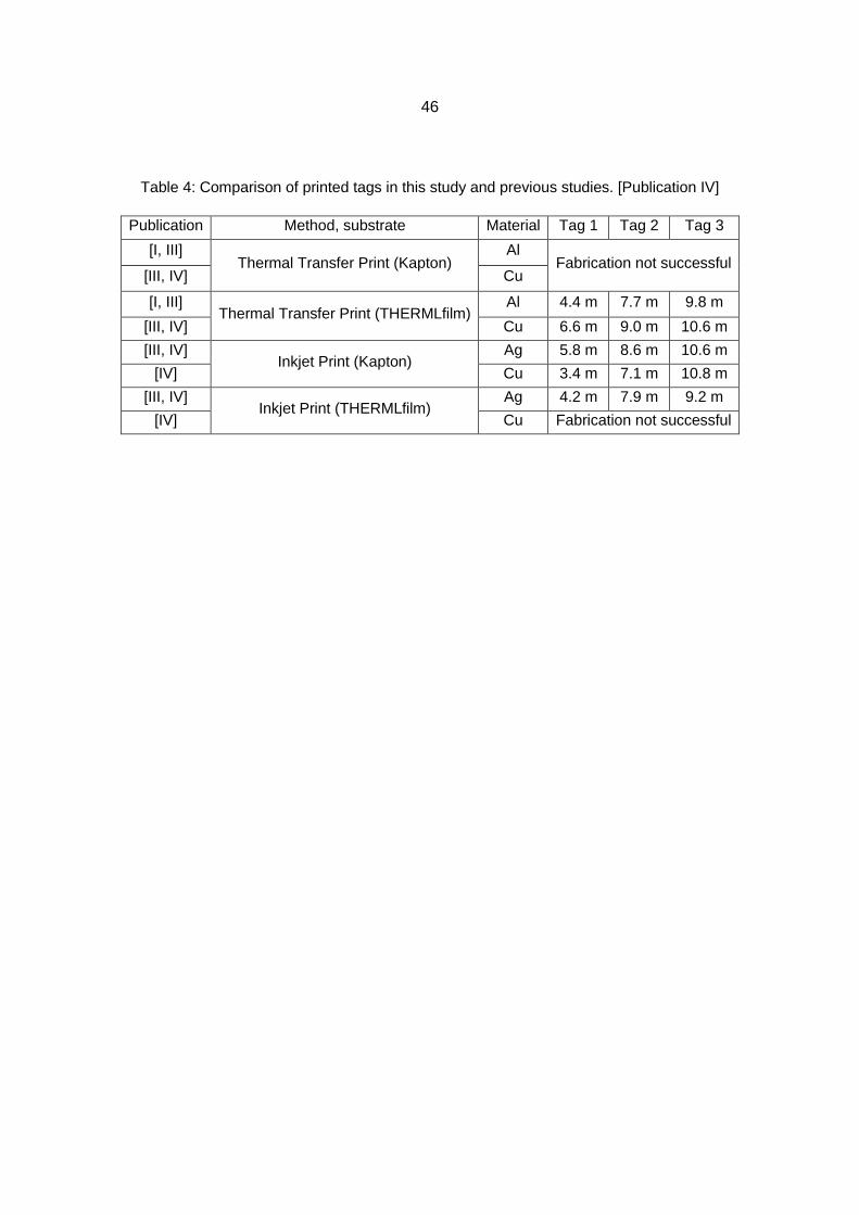
46
Table 4: Comparison of printed tags in this study and previous studies. [Publication IV]
Publication Method, substrate Material Tag 1 Tag 2 Tag 3
[I, III] Thermal Transfer Print (Kapton)
Al Fabrication not successful
[III, IV] Cu
[I, III] Thermal Transfer Print (THERMLfilm)
Al 4.4 m 7.7 m 9.8 m
[III, IV] Cu 6.6 m 9.0 m 10.6 m
[III, IV] Inkjet Print (Kapton)
Ag 5.8 m 8.6 m 10.6 m
[IV] Cu 3.4 m 7.1 m 10.8 m
[III, IV] Inkjet Print (THERMLfilm)
Ag 4.2 m 7.9 m 9.2 m
[IV] Cu Fabrication not successful

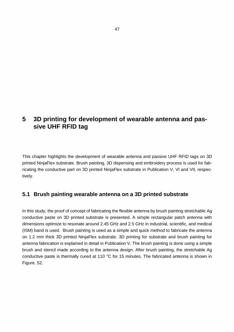
47
This chapter highlights the development of wearable antenna and passive UHF RFID tags on 3D
printed NinjaFlex substrate. Brush painting, 3D dispensing and embroidery process is used for fab-
ricating the conductive part on 3D printed NinjaFlex substrate in Publication V, VI and VII, respec-
tively.
5.1 Brush painting wearable antenna on a 3D printed substrate
In this study, the proof of concept of fabricating the flexible antenna by brush painting stretchable Ag
conductive paste on 3D printed substrate is presented. A simple rectangular patch antenna with
dimensions optimize to resonate around 2.45 GHz and 2.5 GHz in industrial, scientific, and medical
(ISM) band is used. Brush painting is used as a simple and quick method to fabricate the antenna
on 1.2 mm thick 3D printed NinjaFlex substrate. 3D printing for substrate and brush painting for
antenna fabrication is explained in detail in Publication V. The brush painting is done using a simple
brush and stencil made according to the antenna design. After brush painting, the stretchable Ag
conductive paste is thermally cured at 110 °C for 15 minutes. The fabricated antenna is shown in
Figure. 52.
5 3D printing for development of wearable antenna and pas-
sive UHF RFID tag
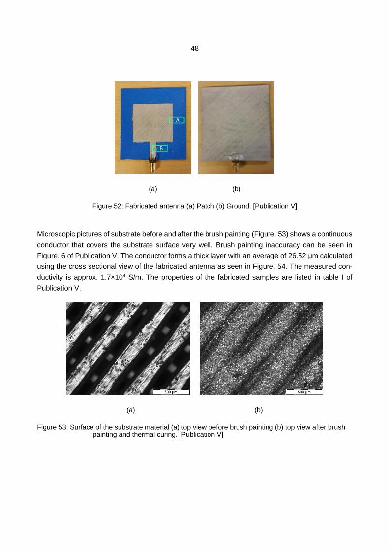
48
(a) (b)
Figure 52: Fabricated antenna (a) Patch (b) Ground. [Publication V]
Microscopic pictures of substrate before and after the brush painting (Figure. 53) shows a continuous
conductor that covers the substrate surface very well. Brush painting inaccuracy can be seen in
Figure. 6 of Publication V. The conductor forms a thick layer with an average of 26.52 μm calculated
using the cross sectional view of the fabricated antenna as seen in Figure. 54. The measured con-
ductivity is approx. 1.7×10⁴ S/m. The properties of the fabricated samples are listed in table I of
Publication V.
(a) (b)
Figure 53: Surface of the substrate material (a) top view before brush painting (b) top view after brush painting and thermal curing. [Publication V]
A
B
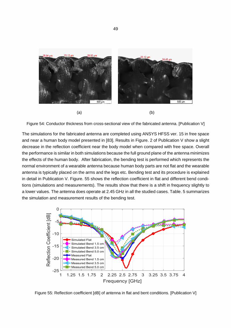
49
(a) (b)
Figure 54: Conductor thickness from cross-sectional view of the fabricated antenna. [Publication V]
The simulations for the fabricated antenna are completed using ANSYS HFSS ver. 15 in free space
and near a human body model presented in [83]. Results in Figure. 2 of Publication V show a slight
decrease in the reflection coefficient near the body model when compared with free space. Overall
the performance is similar in both simulations because the full ground plane of the antenna minimizes
the effects of the human body. After fabrication, the bending test is performed which represents the
normal environment of a wearable antenna because human body parts are not flat and the wearable
antenna is typically placed on the arms and the legs etc. Bending test and its procedure is explained
in detail in Publication V. Figure. 55 shows the reflection coefficient in flat and different bend condi-
tions (simulations and measurements). The results show that there is a shift in frequency slightly to
a lower values. The antenna does operate at 2.45 GHz in all the studied cases. Table. 5 summarizes
the simulation and measurement results of the bending test.
Figure 55: Reflection coefficient [dB] of antenna in flat and bent conditions. [Publication V]
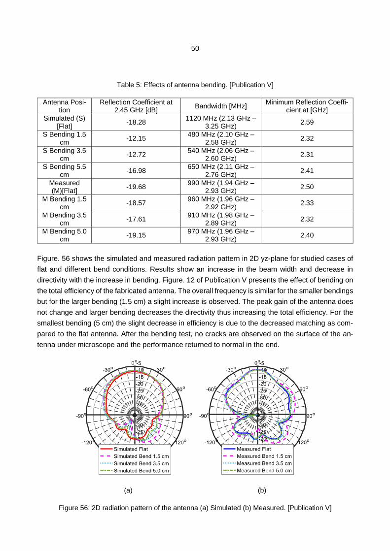
50
Table 5: Effects of antenna bending. [Publication V]
Antenna Posi-tion
Reflection Coefficient at 2.45 GHz [dB]
Bandwidth [MHz] Minimum Reflection Coeffi-
cient at [GHz]
Simulated (S) [Flat]
-18.28 1120 MHz (2.13 GHz –
3.25 GHz) 2.59
S Bending 1.5 cm
-12.15 480 MHz (2.10 GHz –
2.58 GHz) 2.32
S Bending 3.5 cm
-12.72 540 MHz (2.06 GHz –
2.60 GHz) 2.31
S Bending 5.5 cm
-16.98 650 MHz (2.11 GHz –
2.76 GHz) 2.41
Measured (M)[Flat]
-19.68 990 MHz (1.94 GHz –
2.93 GHz) 2.50
M Bending 1.5 cm
-18.57 960 MHz (1.96 GHz –
2.92 GHz) 2.33
M Bending 3.5 cm
-17.61 910 MHz (1.98 GHz –
2.89 GHz) 2.32
M Bending 5.0 cm
-19.15 970 MHz (1.96 GHz –
2.93 GHz) 2.40
Figure. 56 shows the simulated and measured radiation pattern in 2D yz-plane for studied cases of
flat and different bend conditions. Results show an increase in the beam width and decrease in
directivity with the increase in bending. Figure. 12 of Publication V presents the effect of bending on
the total efficiency of the fabricated antenna. The overall frequency is similar for the smaller bendings
but for the larger bending (1.5 cm) a slight increase is observed. The peak gain of the antenna does
not change and larger bending decreases the directivity thus increasing the total efficiency. For the
smallest bending (5 cm) the slight decrease in efficiency is due to the decreased matching as com-
pared to the flat antenna. After the bending test, no cracks are observed on the surface of the an-
tenna under microscope and the performance returned to normal in the end.
(a) (b)
Figure 56: 2D radiation pattern of the antenna (a) Simulated (b) Measured. [Publication V]
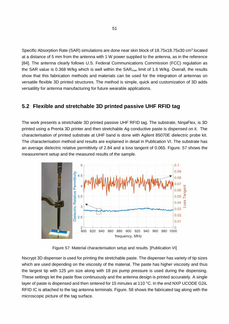
51
Specific Absorption Rate (SAR) simulations are done near skin block of 18.75x18.75x30 cm3 located
at a distance of 5 mm from the antenna with 1 W power supplied to the antenna, as in the reference
[84]. The antenna clearly follows U.S. Federal Communications Commission (FCC) regulation as
the SAR value is 0.368 W/kg which is well within the SARmax limit of 1.6 W/kg. Overall, the results
show that this fabrication methods and materials can be used for the integration of antennas on
versatile flexible 3D printed structures. The method is simple, quick and customization of 3D adds
versatility for antenna manufacturing for future wearable applications.
5.2 Flexible and stretchable 3D printed passive UHF RFID tag
The work presents a stretchable 3D printed passive UHF RFID tag. The substrate, NinjaFlex, is 3D
printed using a Prenta 3D printer and then stretchable Ag conductive paste is dispensed on it. The
characterisation of printed substrate at UHF band is done with Agilent 85070E dielectric probe kit.
The characterisation method and results are explained in detail in Publication VI. The substrate has
an average dielectric relative permittivity of 2.84 and a loss tangent of 0.065. Figure. 57 shows the
measurement setup and the measured results of the sample.
Figure 57: Material characterisation setup and results. [Publication VI]
Nscrypt 3D dispenser is used for printing the stretchable paste. The dispenser has variety of tip sizes
which are used depending on the viscosity of the material. The paste has higher viscosity and thus
the largest tip with 125 μm size along with 18 psi pump pressure is used during the dispensing.
These settings let the paste flow continuously and the antenna design is printed accurately. A single
layer of paste is dispensed and then sintered for 15 minutes at 110 °C. In the end NXP UCODE G2iL
RFID IC is attached to the tag antenna terminals. Figure. 58 shows the fabricated tag along with the
microscopic picture of the tag surface.
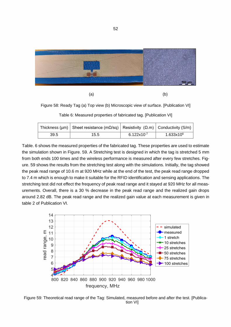
52
(a) (b)
Figure 58: Ready Tag (a) Top view (b) Microscopic view of surface. [Publication VI]
Table 6: Measured properties of fabricated tag. [Publication VI]
Thickness (µm) Sheet resistance (mΩ/sq) Resistivity (Ω.m) Conductivity (S/m)
39.5 15.5 6.122x10⁻⁷ 1.633x10⁶
Table. 6 shows the measured properties of the fabricated tag. These properties are used to estimate
the simulation shown in Figure. 59. A Stretching test is designed in which the tag is stretched 5 mm
from both ends 100 times and the wireless performance is measured after every few stretches. Fig-
ure. 59 shows the results from the stretching test along with the simulations. Initially, the tag showed
the peak read range of 10.6 m at 920 MHz while at the end of the test, the peak read range dropped
to 7.4 m which is enough to make it suitable for the RFID identification and sensing applications. The
stretching test did not effect the frequency of peak read range and it stayed at 920 MHz for all meas-
urements. Overall, there is a 30 % decrease in the peak read range and the realized gain drops
around 2.82 dB. The peak read range and the realized gain value at each measurement is given in
table 2 of Publication VI.
Figure 59: Theoretical read range of the Tag: Simulated, measured before and after the test. [Publica-tion VI]

53
Figure. 60 shows the tag after the stretching test along with the microscopic picture of its surface.
No cracks or permanent elongation is observed after the test and the tags can be considered for the
applications requiring endurance to strain. The overall efficiency of the antenna is estimated to be
around 48% which is better than the antenna efficiency in Publication V. This improved efficiency is
due to the dispensing fabrication method.
(a) (b)
Figure 60: Tag after the stretching test (a) While stretched (b) Microscopic image of surface. [Publica-tion VI]
5.3 Embroidered passive UHF RFID tag on flexible 3D printed substrate
Hybrid fabrication methodology for the manufacturing of a passive UHF RFID tag is presented in
Publication VII. The hybrid fabrication proposed in this study is the combination of 3D printing and
embroidery process. Similar to Publication V and VI, 3D printing is used to make the substrate in this
publication, however, the conductor is not printed instead a Multifilament Ag plated thread is embroi-
dered to make the tag design. The details of 3D printing the NinjaFlex substrate is given in Publica-
tion VII along with the material characterisation at UHF band. The material characterisation is done
in the similar way as explained in Publication VI. The only difference is that the substrate thickness
i.e. 0.5 mm in this study. The thickness is kept low so that the needle of embroidery machine can
easily penetrate the substrate without breaking. The substrate has average dielectric relative permit-
tivity of 1.87 and loss tangent of 0.036.
The ready tag can be seen in Figure. 61 along with microscopic pictures from the top showing the
Ag thread and from the back showing the knots. The NXP UCODE G2iL RFID IC is then attached to
the tag antenna terminals and the wireless measurements are taken after the joint is dried. Figure.
62 (a) shows the measured read range of three fabricated samples of same design along with the
simulations. The substrate characterisation (dielectric and loss tangent) and Ag plated thread (DC
lineal resistivity and thickness) values are used in the simulations to estimate it with more accuracy.
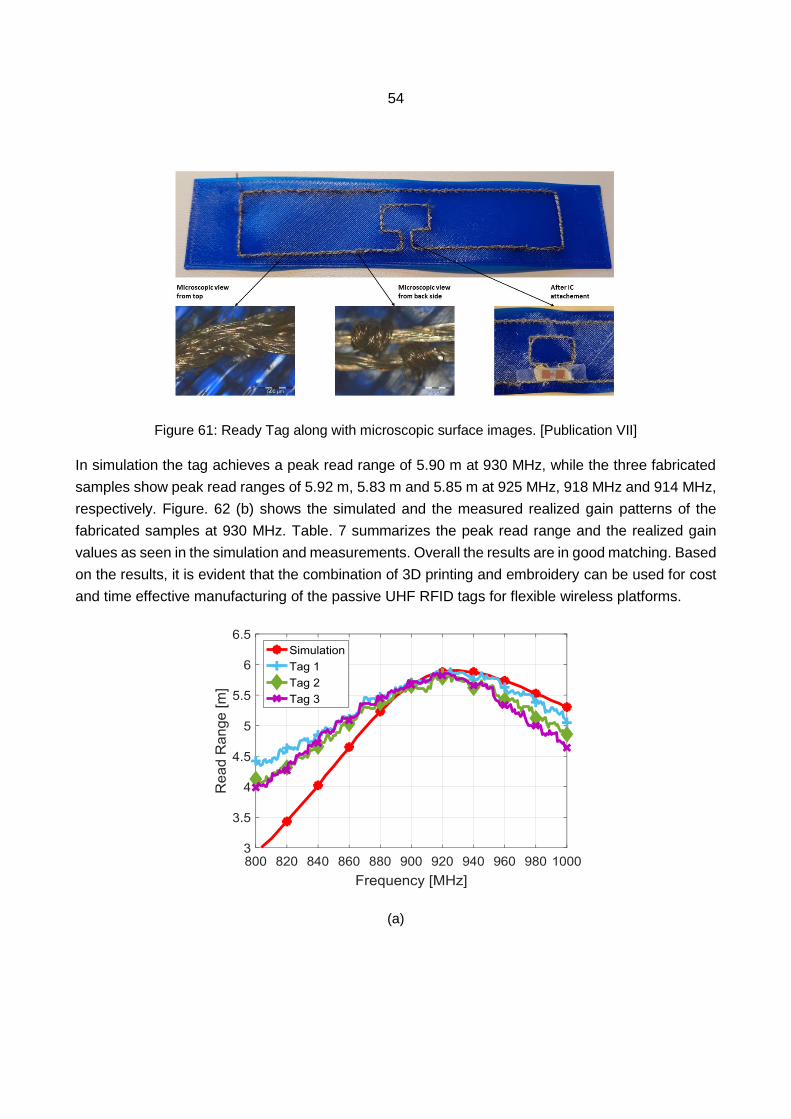
54
Figure 61: Ready Tag along with microscopic surface images. [Publication VII]
In simulation the tag achieves a peak read range of 5.90 m at 930 MHz, while the three fabricated
samples show peak read ranges of 5.92 m, 5.83 m and 5.85 m at 925 MHz, 918 MHz and 914 MHz,
respectively. Figure. 62 (b) shows the simulated and the measured realized gain patterns of the
fabricated samples at 930 MHz. Table. 7 summarizes the peak read range and the realized gain
values as seen in the simulation and measurements. Overall the results are in good matching. Based
on the results, it is evident that the combination of 3D printing and embroidery can be used for cost
and time effective manufacturing of the passive UHF RFID tags for flexible wireless platforms.
(a)
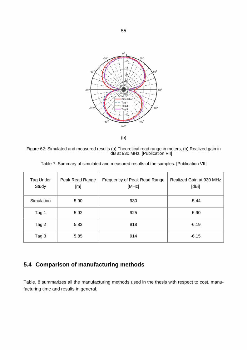
55
(b)
Figure 62: Simulated and measured results (a) Theoretical read range in meters, (b) Realized gain in dB at 930 MHz. [Publication VII]
Table 7: Summary of simulated and measured results of the samples. [Publication VII]
Tag Under
Study
Peak Read Range
[m]
Frequency of Peak Read Range
[MHz]
Realized Gain at 930 MHz
[dBi]
Simulation 5.90 930 -5.44
Tag 1 5.92 925 -5.90
Tag 2 5.83 918 -6.19
Tag 3 5.85 914 -6.15
5.4 Comparison of manufacturing methods
Table. 8 summarizes all the manufacturing methods used in the thesis with respect to cost, manu-
facturing time and results in general.
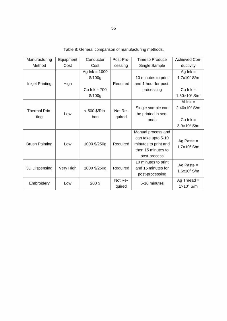
56
Table 8: General comparison of manufacturing methods.
Manufacturing
Method
Equipment
Cost
Conductor
Cost
Post-Pro-
cessing
Time to Produce
Single Sample
Achieved Con-
ductivity
Inkjet Printing High
Ag Ink = 1000
$/100g
Cu Ink = 700
$/100g
Required
10 minutes to print
and 1 hour for post-
processing
Ag Ink =
1.7x10⁷ S/m
Cu Ink =
1.50×10⁷ S/m
Thermal Prin-
ting Low
< 500 $/Rib-
bon
Not Re-
quired
Single sample can
be printed in sec-
onds
Al Ink =
2.40x10⁷ S/m
Cu Ink =
3.9×10⁷ S/m
Brush Painting Low 1000 $/250g Required
Manual process and
can take upto 5-10
minutes to print and
then 15 minutes to
post-process
Ag Paste =
1.7×10⁴ S/m
3D Dispensing Very High 1000 $/250g Required
10 minutes to print
and 15 minutes for
post-processing
Ag Paste =
1.6x10⁶ S/m
Embroidery Low 200 $ Not Re-
quired 5-10 minutes
Ag Thread =
1×10⁴ S/m

57
The thesis focused on finding out how the selected novel materials and manufacturing
methods are combined to produce low-cost, robust, efficient and reliable passive UHF
RFID tags for future wireless applications. The research work is done on material as well
as the antenna part for improving the overall manufacturing of RFID tags. The results
show that novel approaches can be made to fabricate quick, cost-effective and reliable
wireless components for sensing and wearable applications.
The first objective of the thesis was achieved and presented in the Publication I-IV. The
comparison of inkjet and thermal printing was done for the manufacturing of passive UHF
RFID tags on two different substrates. The results showed that inkjet printing can print
on different substrates like polyimide and polyester-based substrates however in thermal
printing the range of compatible substrate is limited by the adhesion of CTTR on the
substrate. The inkjet printed tags outperformed the thermal printed tags in case of theo-
retical read ranges. Afterwards, reliability test was done on tags printed on THERMLfilm.
Two different glues were used to coat the tag IC. The results indicated that the inkjet
printed tags can withstand the high humidity conditions regardless of the glue used how-
ever in case of thermal printed tags, the performance decreased.
The work was extended using Cu based inkjet and thermal printed passive UHF RFID
tags. The reason for using Cu based ink is that it is cheaper than the silver ink and can
give comparable results and a cost-effective solution for manufacturing RFID tags. The
main challenge in using the Cu is that it requires high temperature for reduction. The
substrates under test cannot withstand such high temperatures thus photonic sintering
was used as a post-processing method for inkjet printed tags. According to the results,
the Cu based tags showed better performance as compared to the previously printed
6 Conclusions

58
tags. However photonic sintering was not able to produce a conductive trace on THERM-
Lfilm with the inkjet printed Cu nano-particle ink even after improving the adhesion with
oxygen plasma treatment.
The second objective, development of flexible 3D printed passive UHF RFID tags and
wearable antennas, was achieved in the work presented in Publication V-VII. Initially,
proof-of-concept of fabricating flexible antenna on the 3D printed NinjaFlex substrate by
brush painting stretchable Ag conductive paste was studied. NinjaFlex material is flexible,
customizable and inexpensive. The paste adds more flexibility to the antenna for adopt-
ing the wearable environment near human body. The performance of the antenna was
tested in flat and bend conditions and the results showed that the antenna can operates
well in all of them. The antenna also satisfied the SAR limit imposed by U.S FCC regu-
lations.
The final conductivity and the efficiency of the antenna was low but better wireless prop-
erties were observed by using 3D dispensing with the same material and fabricating a
flexible and stretchable 3D printed passive UHF RFID tag. The novelty of the work in-
cluded the characterisation of 100% infill rectilinear printed Ninjaflex for complete UHF
band, dispensing stretchable silver paste and then studying the impact of stretching on
the tag’s performance. The fabricated tag was stretched multiple times and wireless
measurements were done. Results showed that the tags can withstand extreme stretch-
ing and peak read range (10.56 m) dropped around 30 % (7.35 m) after 100 stretches.
No cracks or permanent elongation was observed after the test and the tags showed
great potential to be used in applications that require endurance to strain. In the end,
hybrid fabrication methodology was proposed by the combination of 3D printing and em-
broidery process for the manufacturing of passive UHF RFID tags. Only the contour or
the outer boundary of the design was embroidered and the tag showed 5.92 m peak read
range which is very good as compared to the tag performance in previous studies con-
sidering that less conductor was used by the embroidery process. The results showed
that the methodology can be used for cost and time effective RFID fabrication along with
suitable performance for wireless sensing applications.
6.1 Major contributions of the thesis
As mentioned earlier, the thesis contributes towards the novel manufacturing methods
for the development of passive UHF RFID tags and wearable antennas on versatile sub-
strates. Few of the major contributions of the thesis are:

59
1. Exploring thermal printing for the fabrication of passive UHF RFID tags on Kapton
and THERMLfilm substrates with different conductive materials.
2. Comparison of inkjet printing and thermal printing for the fabrication of passive
UHF RFID tags and their reliability study in high humidity conditions.
3. 3D printing and characterizing flexible NinjaFlex substrate with different thickness,
i.e. 1.2 mm and 0.5 mm, at UHF band. Utilizing NinjaFlex as substrate for RFID
and wearable antenna study.
4. Brush painting stretchable conductive paste for the manufacturing of wearable
antenna on 3D printed substrate.
5. Manufacturing flexible and stretchable 3D printed passive UHF RFID tag. The
results of the tag show that it can be used as a sensor in applications where strain
is a concern.
6. Embroidered passive UHF RFID tag on 3D printed substrate. The tag maintained
good performance with only a contour design of the tag and can be used as
wearable sensor in body area networks.
6.2 Future research recommendations
All the research done in this thesis is mostly based on experiments. The results are very
promising however there are certain aspects that still need further research such as:
1) Exploring more suitable substrates for thermal printing.
2) 3D printing of substrate with different infills and its effect on the antenna performance.
3) Exploring flexible conductive materials that can be 3D printed on NinjaFlex.
Huge potential lies in these fabrication methodologies and with optimization for specific
substrate or customized printed substrate, overall fabrication process can be improved
in terms of time, cost and efficiency. Results obtained in this dissertation provide a path-
way for benefiting from the manufacturing methods to produce better smart products for
future wireless applications.

60
References
[1] X. Jia, Q. Feng, T. Fan, and Q. Lei, “RFID technology and its applications in Internet
of Things (IoT),” Proc. Int. Conf. Consum. Electron. Commun. Netw. (CECNet), pp.
1282-1285, Apr. 2012.
[2] KuBo, “The research of IoT based on RFID technology,” International Conference on
Intelligent Computation Technology and Automation., pp. 832-835, Jan. 2015.
[3] S. Dominikus, M.J. Aiger, and S. Kraxberger, “Passive RFID technology for the Internet
of Things,” International Conference for Internet Technology and Secured
Transactions (ICITST), pp. 1-8, Nov. 2010.
[4] K. Finkenzeller, “RFID Handbook: Radio-Frequency Identification Fundamentals and
Applications” Wiley, New York, 2003.
[5] D. Dobkin, “The RF in RFID: passive UHF RFID in practice” Elesvier, New York, 2007.
[6] R. Want, “An introduction to RFID technology,” IEEE Pervasive Computing, vol. 5, no.
1, pp. 25-33, Mar. 2006.
[7] F. J. Valente and A. C. Neto, “Intelligent steel inventory tracking with IoT / RFID,” IEEE
International Conference on RFID Technology & Application (RFID-TA), pp. 158-163,
Nov. 2017.
[8] D. Zhang, L. T. Yang, M. Chen, S. Zhao, M. Guo, and Y. Zhang, “Realtime locating
systems using active RFID for Internet of Things,” IEEE Syst. J., vol. 10, no. 3, pp.
1226-1235, Sep. 2016.
[9] G. Xiao, P. Aflaki, S. Lang, Z. Zhang, Y. Tao, C. Py, P. Lu, C. Martin and S. Chang,
“Printed UHF RFID Reader Antennas for Potential Retail Applications,” IEEE Journal
of Radio Frequency Identification, Apr. 2018.
[10] P. Bilski et al., “Application of the RFID technology in the European Union border
control system,” IEEE International Conference on RFID Technology & Application
(RFID-TA), pp. 28-33, Nov. 2017.
[11] S. Karuppuswami, L. L. Matta, E. C. Alocilja and P. Chahal, “A wireless RFID
compatible sensor tag using gold nanoparticle markers for pathogen detection in the
liquid food supply chain,” IEEE Sensors Letters, Apr. 2018.
[12] S. Javaid, A. Sufian, S. Pervaiz and M. Tanveer, “Smart traffic management system
using Internet of Things,” International Conference on Advanced Communication
Technology (ICACT), pp. 393-398, Mar. 2018.
61
[13] A. Vena, L. Sydänheimo, L. Ukkonen and M. M. Tentzeris, “A fully inkjet-printed
chipless RFID gas and temperature sensor on paper,” IEEE RFID Technology and
Applications Conference (RFID-TA), pp. 115-120, Oct. 2014.
[14] R. Baccarelli, G. Orecchini, F. Alimenti and L. Roselli, “Feasibility study of a fully
organic, CNT based, harmonic RFID gas sensor,” IEEE International Conference on
RFID-Technologies and Applications (RFID-TA), pp. 419-422, Jan. 2012.
[15] I. Jauregi et al., “UHF RFID Temperature Sensor Assisted With Body-Heat Dissipation
Energy Harvesting,” IEEE Sensors Journal, vol. 17, no. 5, pp. 1471-1478, Mar. 2017.
[16] M. C. Caccami, M. P. Hogan, M. Alfredsson, G. Marrocco and J. C. Batchelor, “A
Tightly Integrated Multilayer Battery Antenna for RFID Epidermal Applications,” IEEE
Transactions on Antennas and Propagation, vol. 66, no. 2, pp. 609-617, Feb. 2018.
[17] S. Yang, M. Crisp, R. V. Penty and I. H. White, “RFID Enabled Health Monitoring
System for Aircraft Landing Gear,” IEEE Journal of Radio Frequency Identification, Apr.
2018.
[18] X. Hui and E. C. Kan, “Mitigation of body movement interference in near-field coherent
sensing for heartrate monitoring,” IEEE International Conference on Wearable and
Implantable Body Sensor Networks (BSN), pp. 156-159, Apr. 2018.
[19] F. Calignano et al., “Overview on additive manufacturing technologies,” Proc. IEEE,
vol. 105, no. 4, pp. 593-612, Apr. 2017.
[20] S. A. Nauroze et al., “Additively manufactured RF components and modules: Toward
empowering the birth of cost-efficient dense and ubiquitous IoT implementations,”
Proceedings of the IEEE, vol. 105, no. 4, pp. 702-722, Apr. 2017.
[21] L. Yang, A. Rida, R. Vyas and M. M. Tentzeris, “RFID tag and RF structures on paper
substrates using inkjet-printing technology,” IEEE Transactions on Microwave Theory
and Techniques, vol. 55, no. 12, pp. 2894-2901, Dec. 2007.
[22] M. M. Tentzeris, K Sangkil, A. Traille, H. Aubert, K. Yoshihiro, A. Georgiadis and A.
Collado, “Inkjet-printed RFID-enabled sensors on paper for IoT and “Smart Skin”
applications,” International Conference on Applied Electromagnetics and
Communications (ICECom), pp. 1-4, Oct. 2013.
[23] S. Kim, Y. Kawahara, A. Georgiadis, A. Collado, and M. M. Tentzeris, “Low-cost inkjet-
printed fully passive RFID tags for calibrationfree capacitive/haptic sensor applications,”
IEEE Sensors J., vol. 15, pp. 3135-3145, Jun. 2015.
[24] R. Singh, E. Singh and H. S. Nawla, “Inkjet printed nanomaterial based flexible radio
frequency identification (RFID) tag sensors for the internet of nano things,” RSC
Advances, Issue 77, pp. 48597-48630, Sept. 2017.

62
[25] Y. Ren, J. Virkki, L. Sydänheimo and L. Ukkonen, “Optimisation of manufacturing
parameters for inkjet-printed and photonically sintered metallic nanoparticle UHF RFID
tags,” Electronics Letters, vol. 50, no. 21, pp. 1504-1505, Octo. 2014.
[26] M. Kgwadi, C. J. Vourch, D. J. Harrison and T.D. Drysdale, “On-demand printing of
antennas for TV white-space communications,” Loughborough Antennas and
Propagation Conference (LAPC), pp. 553-556, Nov. 2014.
[27] K. V. Hoel, S. Kristoffersen, J. Moen, K. G. Kjelgård and T. S. Lande, “Broadband
antenna design using different 3D printing technologies and metallization processes,”
European Conference on Antennas and Propagation (EuCAP), pp. 1-5, Jun. 2016.
[28] S. H. Naushahi, K. Rasilainen and V. Viikari, “Realization of RFID tag antenna with 3D
printing technology,” European Conference on Antennas and Propagation (EuCAP),
pp. 1-4, Jun. 2016.
[29] B. Sanz-Izquierdo and J. Sungyun, “WLAN antenna on 3D printed bracelet and wrist
phantom,” Loughborough Antennas and Propagation Conference (LAPC), pp. 372-375,
Dec. 2014.
[30] W. G. Whittow, “3D printing, inkjet printing and embroidery techniques for wearable
antennas,” European Conference on Antennas and Propagation (EuCAP), pp. 1-4, Jun.
2016.
[31] M. Ahmadloo and P. Mousavi, “Application of novel integrated dielectric and
conductive ink 3D printing technique for fabrication of conical spiral antennas,” IEEE
Antennas and Propagation Society International Symposium, pp. 780-781, Jul. 2013.
[32] M. Attaran, “The rise of 3-D printing: The advantages of additive manufacturing over
traditional manufacturing,” Business Horizons, vol. 60, Issue 5, pp. 677-688, 2017.
[33] Harima NPS-JL silver nanoparticle ink,
https://www.harima.co.jp/en/products/electronics/pdf/brochure16e_23.pdf (Accessed
on 12th Jan 2018)
[34] ANI Cu-IJ70 Cu nanoparticle ink,
http://nebula.wsimg.com/f356531a3cd44d6939147efb4932fed6?Access-
KeyId=D6756B5639AB3254C10B&disposition=0&alloworigin=1 (Accessed on 12th
Jan 2018)
[35] DuPont PE872
http://www.dupont.com/ (Accessed on 12th Jan 2018)
[36] K. Finkenzeller, “RFID Handbook: Fudamentals and Applications in Contactless Smart
Cards and Identification” West Sussex: John Wiley & Sons Ltd., 2003.
[37] R. Das and P. Harrop, “RFID forecasts, players and opportunities 2011-2021”
IDTechEx, 2011.
63
[38] V. D. Hunt, A. Puglia and M. Puglia, “RFID-A Guide to Radio Frequency Identification”
Hoboken, NJ: Wiley, 2007.
[39] A.B. Constantine, “Antenna Theory: Analysis and Design”, 3rd ed., John Wiley & Sons,
Inc. 2005.
[40] J.D. Kraus, “Antennas for All Applications”, 3rd Edition, USA, McGraw-Hill. 2002. 921
p.
[41] W. Stutzman and G. Thiele, “Antenna Theory and Design”, 2nd ed., Hoboken, New
Jersey: John Wiley & Sons, Inc., 1998.
[42] K. Kurokawa, “Power waves and the scattering matrix,” IEEE Transactions on
Microwave Theory and Techniques, vol. 13, no. 2, pp. 194-202, Mar. 1965.
[43] P. Nikitin, K. Rao, S. Lam, V. Pillai, R. Martinez and H. Heinrich, “Power reflection
coefficient analysis for complex impedances in RFID tag design,” IEEE Transactions
on Microwave Theory and Techniques, vol. 53, no. 9, pp. 2721-2725, Sept. 2005.
[44] P. Nikitin, K. Rao, R. Martinez and S. Lam, “Sensitivity and impedance measurements
of UHF RFID chips,” IEEE Transactions on Microwave Theory and Techniques, vol.
57, no. 5, pp. 1297-1302, Mar. 2009.
[45] G. Marrocco, “The art of UHF RFID antenna design: impedance-matching and size-
reduction techniques,” IEEE Antennas and Propagation Magazine, vol. 50, no. 1, pp.
66-79, Apr. 2008.
[46] K. Rao, P. Nikitin and S. Lam, “Antenna design for UHF RFID tags: a review and a
practical application,” IEEE Transactions on Antennas and Propagation, vol. 53, no.
12, pp. 3870-3876, 2005.
[47] V. Cerbek, C. Steger, R. Weiss, J. Preishuber-Pflügl and M. Pistauer, “A UHF
measurement and evaluation test system,” Elektrotechnik & Informationstechnik, Vol.
124, No. 11, pp. 384-390, Oct. 2007.
[48] K. V. S. Rao, P. V. Nikitin and S. F. Lam, “Impedance matching concepts in RFID
transponder design,” IEEE Workshop on Automatic Identification Advanced
Technologies, ser. AUTOID ’05, pp. 39-42, Dec. 2005.
[49] NXP UCODE G2iL IC Datasheet,
http://www.nxp.com/documents/data_sheet/SL3S1203_1213.pdf (Accessed on 12th
Jan 2018).
[50] T. Björninen, L. Sydänheimo and L. Ukkonen, “Development and validation of an
equivalent circuit model for UHF RFID IC based on wireless tag measurements,”
Antenna Measurement Techniques Association Symposium, 21-26 Oct., 2012,
Bellevue, WA.

64
[51] J. Virtanen, J. Virkki, L. Sydänheimo, M. Tentzeris, and L. Ukkonen, “Automated
identification of plywood using embedded inkjet-printed passive UHF RFID tags,” IEEE
Transactions on Automation Science and Engineering, vol. 10, no. 3, pp. 796-806, Jul.
2013.
[52] I. Gibson, D. Rosen and B. Stucker, “Additive Manufacturing Technologies: 3D Printing,
Rapid Prototyping, and Direct Digital Manufacturing” New York: Springer, 2015,
Second Edition.
[53] J. A. Lewis and G. M. Gratson, “Direct writing in three dimensions,” Materials Today,
vol. 7, no. 7-8, pp. 32-39, Aug. 2004.
[54] L. Mortara, J. Hughes, P. S. Ramsundar, F. Livesey and D. R. Probert, “Proposed
classification scheme for direct writing technologies,” Rapid Prototyping Journal, vol.
15, no. 4, pp. 299-309, 2009.
[55] J. Niittynen, “Comparison of sintering methods and conductive adhesives for
interconnections in inkjet-printed flexible electronics,” Ph.D. dissertation, Tampere
University of Technology, 2015.
[56] Y. Kim, B. Lee, S. Yang, I. Byun, I. Jeong and S. M. Cho, “Use of copper ink for
fabricating conductive electrodes and RFID antenna tags by screen printing,” Current
Applied Physics, vol. 12, No. 2, pp. 473-478, Mar. 2012.
[57] Y. Amin, Q. Chen, L.-R. Zheng and H. Tenhunen, “Design and fabrication of wideband
archimedean spiral antenna based ultra-low cost “Green” Modules for RFID Sensing
and Wireless Applications,” Progress In Electromagnetics Research (PIER), vol. 130,
pp. 241-256, 2012.
[58] K. Church et al., “Printed electronic processes for flexible hybrid circuits and antennas,”
Flexible Electronics & Displays Conference and Exhibition, pp. 1-7, Jun. 2009.
[59] P. Salonen, V. Kupiainen and M. Tuohimaa, “Direct printing of a handset antenna on
a 3D surface,” IEEE International Symposium on Antennas and Propagation Society
(APSURSI), pp. 504-505, Jan. 2013.
[60] nScrypt 3Dn series datasheet
http://nscrypt.com/wp-content/uploads/2015/08/nScrypt-3Dn-Brochure.pdf (Accessed
on 12th Jan 2018)
[61] E. Sipilä, J. Virkki, J. Wang, L. Sydänheimo and L. Ukkonen, “Brush-painting and
photonical sintering of copper oxide and silver inks on wood and cardboard substrates
to form antennas for UHF RFID tags,” International Journal of Antennas and
Propagation, vol. 2016, Article ID 3694198, 8 pages, Apr. 2016.
[62] M. Kgwadi and T. D. Drysdale, “Diode-switched thermal-transfer printed antenna on
flexible substrate,” Electronics Letters, vol. 52, no. 4, pp. 258-260, Feb. 2016.

65
[63] Zebra S4M Thermal Printer
https://www.zebra.com/content/dam/zebra/manuals/en-us/printer/s4m-ug-en.pdf
(Accessed on 12th Jan 2018)
[64] H. Lipson and M. Kurman, “Fabricated: The New World of 3D Printing” Wiley, USA,
2013.
[65] M. Mirzaee and S. Noghanian, “Additive manufacturing of a compact 3D dipole
antenna using ABS thermoplastic and high temperature carbon paste,” IEEE
International Symposium on Antennas and Propagation (APSURSI), pp. 475-476, Jun.
2016.
[66] M. Hoyack, J. Bjorgaard, E. Huber, M. Mirzaee and S. Noghanian, “Connector design
for 3D printed antennas,” IEEE International Symposium on Antennas and Propagation
(APSURSI), pp. 477-478, Jun. 2016.
[67] M. Mirzaee, S. Noghanian, L. Wiest and I. Chang, “Developing flexible 3D printed
antenna using conductive ABS materials,” IEEE International Symposium on Antennas
and Propagation & USNC/URSI National Radio Science Meeting, pp. 1308-1309, Jul.
2015.
[68] K. Nate and M. M. Tentzeris, “A novel 3-D printed loop antenna using flexible NinjaFlex
material for wearable and IoT applications,” IEEE Electrical Performance of Electronic
Packaging and Systems (EPEPS), pp. 171-174, Oct. 2015.
[69] S. Moscato et al., “Infill dependent 3-D Printed material based on ninjaflex filament for
antenna applications,” IEEE Antennas and Wireless Propagation Letters, vol. 15, no.
pp. 1506-1509, Jan. 2016.
[70] Prenta Duo 3D Printer
http://www.prenta.fi (Accessed on 12th Jan 2018)
[71] A. Tsolis, W. G. Whittow, A. A. Alexandridis, and J. C. Vardaxoglou, “Embroidery and
related manufacturing techniques for wearable antennas: Challenges and
opportunities,” Electronics, vol. 3, pp. 314-338, May 2014.
[72] R. Rahimi, W. Yu, T. Parupudi, M. Ochoa, and B. Ziaie, “A low-cost fabrication
technique for direct sewing stretchable interconnetions for wearable electronics,”
International Conference on Solid State Sensors, Actuators and Microsystems
(TRANSDUCERS), pp. 1350-1353, Jun. 2015.
[73] S. P. Pinapati, D. C. Ranasinghe and C. Fumeaux, “Characterization of conductive
textiles for wearable RFID applications,” International Conference on Electromagnetics
in Advanced Applications (ICEAA), pp. 341-344, Nov. 2016.
[74] Husqvarna Viking embroidery
http://www.husqvarnaviking.com/Machines/DESIGNER-RUBY-Royale (Accessed on
12th Jan 2018)

66
[75] Shieldex, 110f34 dtex 2-ply HC, High Grade Multifilament Nylon Yarn, 2014
http://www.shieldextrading.net/products/yarns-threads/ (Accessed on 12th Jan 2018)
[76] J. Niittynen, R. Abbel, M. Mäntysalo, J. Perelaer, U. S. Schubert, and D. Lupo,
“Alternative sintering methods compared to conventional thermal sintering for inkjet
printed silver nanoparticle ink,” Thin Solid Films, vol. 556, pp. 452-459, Apr. 2014.
[77] Xenon Sinteron 2010-L. Installation and User Manual. Xenon Corporation, June 2013.
[78] J. Virtanen, J. Virkki, A. Z. Elsherbeni, L. Sydänheimo and L. Ukkonen, “A selective ink
deposition method for the cost-performance optimization of inkjet-printed UHF RFID
tag antennas,” International Journal of Antennas and Propagations, vol. 2012, pp. 1-9,
Mar. 2012.
[79] J. Virkki, J. Virtanen, L. Sydänheimo, M.M. Tentzeris, L. Ukkonen, “Embedding Inkjet-
printed antennas into plywood structures for identification and sensing,” IEEE
International conference on RFID Technology and Applications, pp. 34-39, Jan. 2012.
[80] M. Akbari, et al. “Fabrication and characterization of graphene antenna for low-cost
and environmentally friendly RFID tags,” IEEE Antennas Wireless Propagation Letters,
vol. 15, pp. 1569-1572, Nov. 2016.
[81] S. Enderling et al., “Sheet resistance measurement of non-standard cleanroom
materials using suspended Greek cross test structures,” IEEE Transactions on
Semiconductor Manufacturing, vol. 19, no. 1, pp. 2-9, Feb. 2006.
[82] Y. Wei, Y. Li, R. Torah and J. Tudor, “Laser curing of screen and inkjet printed
conductors on flexible substrates,” Symposium on Design, Test, Integration and
Packaging of MEMS/MOEMS (DTIP), pp. 1-4, Jul. 2015.
[83] S. M. Abbas, K. P. Esselle and Y. Ranga, “A printed dual band antenna with a ground
plane and electromagnetically-coupled feed for wireless body area networks,”
International Workshop on Antenna Technology: Small Antennas, Novel EM Structures
and Materials, and Applications (iWAT), pp. 15-17, Nov. 2014.
[84] M. W. A. Khan, T. Björninen, L. Sydänheimo and L. Ukkonen, “Characterization of two-
turns external loop antenna with magnetic core for efficient wireless powering of
cortical implants,” IEEE Antennas and Wireless Propagation Letters, vol. 15, pp.1410-
1413, Dec. 2016.

ISBN 978-952-15-4181-0
ISSN 1459-2045
Tampereen teknillinen yliopisto PL 52733101 Tampere
Tampere University of TechnologyP.O.B. 527FI-33101 Tampere, Finland