mtacca/courses/ee3120/spring-2007/ise... · web view3.1 opening a project 3.2 creating an verilog...
TRANSCRIPT

Digital Circuit Design Using Xilinx ISE Tools
Table of Contents
1. Introduction 2. Programmable logic devices: FPGA3. Creating a new project in Xilinx ISE 3.1 Opening a project 3.2 Creating an Verilog input file for a combinational logic design 3.3 Editing the Verilog source file4. Compilation and Implementation of the Design5. Functional Simulation of Combinational Designs 5.1 Adding the test vectors 5.2 Simulating and viewing the simulation result waveforms 5.3 Saving the simulation results6. Preparing and downloading bitstream for the Spartan FPGA7. Testing a Digital logic circuit 7.1 Observing the outputs using the on-board LEDs and Seven Segment Display8. Design and Simulation of sequential circuits using Verilog 9.1 Design of Sequential Circuits 9.2 Simulation of Sequential Circuits9. Hierarchical circuit design using Modules
Appendix:
A. Verilog Hardware Modeling – Introduction to Verilog Language.

1. Introduction
Xilinx Tools is a suite of software tools used for the design of digital circuits implemented using Xilinx Field Programmable Gate Array (FPGA) or Complex Programmable Logic Device (CPLD). The design procedure consists of (a) design entry, (b) compilation and implementation of the design, (c) functional simulation and (d) testing and verification. Digital designs can be entered in various ways using the above CAD tools: using a schematic entry tool, using a hardware description language (HDL) – Verilog or VHDL or a combination of both. In this lab we will only use the design flow that involves the use of Verilog HDL.
The CAD tools enable you to design combinational and sequential circuits starting with Verilog HDL design specifications. The steps of this design procedure are listed below:
1. Create Verilog design input file(s) using template driven editor. 2. Compile and implement the Verilog design file(s). 3. Create the test-vectors and simulate the design (functional simulation) without using a
PLD (FPGA or CPLD). 4. Assign input/output pins to implement the design on a target device. 5. Download bitstream to an FPGA or CPLD device. 6. Test design on FPGA/CPLD device
A Verilog input file in the Xilinx software environment consists of the following segments: Header: module name, list of input and output ports. Declarations: input and output ports, registers and wires. Logic Descriptions: equations, state machines and logic functions. End: endmodule
All your designs for this lab must be specified in the above Verilog input format. Note that the state diagram segment does not exist for combinational logic designs.
2. Programmable Logic Device: FPGA
In this lab digital designs will be implemented in the Pegasus board which has a Xilinx Spartan FPGA XC2S50. This FPGA part belongs to the Spartan family of FPGAs. These devices come in a variety of packages. We will be using devices that are packaged in 208 pin package with the following part number: XC2S50-PQ208. This FPGA is a device with about 50K gates. Detailed information on this device is available at the Xilinx website.

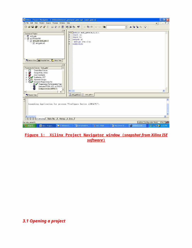
3. Creating a New Project Xilinx Tools can be started by clicking on the Project Navigator Icon on the Windows desktop. This should open up the Project Navigator window on your screen. This window shows (see Figure 1) the last accessed project.
Figure 1: Xilinx Project Navigator window ( snapshot from Xilinx ISE software )
3.1 Opening a project
Select File->New Project to create a new project. This will bring up a new project window (Figure 2) on the desktop. Fill up the necessary entries as follows:
Figure 2: New Project Initiation window ( snapshot from Xilinx ISE software)
Project Name: Write the name of your new project Project Location:The directory where you want to store the new project
Leave the top level module type as HDL.
Example: If the project name were “or_gate”, enter “or_gate” as the project name and then click “Next”.

Clicking on NEXT should bring up the following window:
Figure 3: Device and Design Flow of Project ( snapshot from Xilinx ISE software)
For each of the properties given below, click on the ‘value’ area and select from the list of values that appear.
o Device Family: Family of the FPGA/CPLD used. In this laboratory we will be using the Spartan2 FPGA’s.
o Device: The number of the actual device. For this lab you may enter XC2S50 (this can be found on the attached prototyping board)
o Package: The type of package with the number of pins. The Spartan FPGA used in this lab is packaged in PQ208 package.
o Speed Grade: The Speed grade is “-6”.
o Synthesis Tool: XST [VHDL/Verilog]
o Simulator: The tool used to simulate and verify the functionality of the design. Modelsim simulator is integrated in the Xilinx ISE. Hence choose “Modelsim” as the simulator.
o Then click on NEXT to save the entries.

All project files such as schematics, netlists, Verilog files, VHDL files, etc., will be stored in a subdirectory with the project name. A project can only have one top level HDL source file (or schematic). Modules can be added to the project to create a modular, hierarchical design (see Section 9).
In order to open an existing project in Xilinx Tools, select File->Open Project to show the list of projects on the machine. Choose the project you want and click OK.
Clicking on NEXT on the above window brings up the following window:
Figure 4: Create New source window ( snapshot from Xilinx ISE software)
If creating a new source file, Click on the NEW SOURCE.
3.2 Creating a Verilog HDL input file for a combinational logic design

In this lab we will enter a design using a structural or RTL description using the Verilog HDL. You can create a Verilog HDL input file (.v file) using the HDL Editor available in the Xilinx ISE Tools (or any text editor).
If adding an already existing source file (.v file) to the project, in the project Navigator window, select Project -> Add Copy Source and browse through the disk for the source file.
If creating a new source file, in the Project Navigator window, select Project -> New Source. A window pops up as shown in Figure 4. (Note: “Add to project” option is selected by default. If you do not select it then you will have to add the new source file to the project manually.)
Figure 5: Creating Verilog-HDL source file ( snapshot from Xilinx ISE software )
Select Verilog Module and in the “File Name:” area, enter the name of the Verilog source file you are going to create. Also make sure that the option Add to project is selected so that the source need not be added to the project again. Then click on Next to accept the entries. This pops up the following window (Figure 5).

Figure 6: Define Verilog Source window ( snapshot from Xilinx ISE software )
In the Port Name column, enter the names of all input and output pins and specify the Direction accordingly. A Vector/Bus can be defined by entering appropriate bit numbers in the MSB/LSB columns. Then click on Next> to get a window showing all the new source information (Figure 6). If any changes are to be made, just click on <Back to go back and make changes. If everything is acceptable, click on Finish to continue.

Figure 7: New Project Information window( snapshot from Xilinx ISE software )
Once you click on Finish, the source file will be displayed in the sources window in the Project Navigator (Figure 1).
If a source has to be removed, just right click on the source file in the Sources in Project window in the Project Navigator and select Remove in that. Then select Project -> Delete Implementation Data from the Project Navigator menu bar to remove any related files.
3.3 Editing the Verilog source file
The source file will now be displayed in the Project Navigator window (Figure 8). The source file window can be used as a text editor to make any necessary changes to the source file. All the input/output pins will be displayed. Save your Verilog program periodically by selecting the File->Save from the menu. You can also edit Verilog programs in any text editor and add them to the project directory using “Add Copy Source”.

Figure 8: Verilog Source code editor window in the Project Navigator ( from Xilinx ISE software )
Adding Logic in the generated Verilog Source code template:
A brief Verilog Tutorial is available in Appendix-A. Hence, the language syntax and construction of logic equations can be referred to Appendix-A.
The Verilog source code template generated shows the module name, the list of ports and also the declarations (input/output) for each port. Combinational logic code can be added to the verilog code after the declarations and before the endmodule line.
For example, an output z in an OR gate with inputs a and b can be described as, assign z = a | b; Remember that the names are case sensitive.
Other constructs for modeling the logic function:

A given logic function can be modeled in many ways in verilog. Here is another example in which the logic function, is implemented as a truth table using a case statement:
module or_gate(a,b,z);input a;input b;output z;
reg z;
always @(a or b)begin
case ({a,b}) 00: z = 1'b0; 01: z = 1'b1; 10: z = 1'b1; 11: z = 1'b1; endcase
endendmodule
Suppose we want to describe an AND gate. It can be done using the logic equation as shown in Figure 9a or using the case statement (describing the truth table) as shown in Figure 9b. These are just two example constructs to design a logic function. Verilog offers numerous such constructs to efficiently model designs. A brief tutorial of Verilog is available in Appendix-A.
Figure 9a: OR gate description using assign statement ( snapshot from Xilinx ISE software )

Figure 9b: OR gate description using case statement ( from Xilinx ISE software )
4. Compilation and Implementation of the Design The design has to be compiled and implemented before it can be checked for correctness, by running functional simulation or downloaded onto the prototyping board. With the top-level Verilog file opened (can be done by double-clicking that file) in the HDL editor window in the right half of the Project Navigator, and the view of the project being in the Module view , the implement design option can be seen in the process view. Design entry utilities and Create Programming File options can also be seen in the process view. The former can be used to include user constraints, if any and the latter will be discussed later.
To compile the design, expand the Implement design option by clicking on the ‘add’ sign in front of the implement design tab. Now click on the option Compile Design in the Processes window. It will go through steps like Check Syntax, Compile Logic, Interpret Feedbacks, Reformat Logic and Optimize Hierarchy. If any of these steps could not be done or done with errors, it will place a X mark in front of that, otherwise a tick mark will be placed after each of them to indicate the successful completion. If everything is done successfully, a tick mark will be placed
before the Compile Design option. If there are warnings, one can see mark in front of the option indicating that there are some warnings. One can look at the warnings or errors in the Console window present at the bottom of the Navigator window. Every time the design file is saved; all these marks disappear asking for a fresh compilation.
To implement the design, double-click on the Implement Design option. It has many steps in it e.g., Translation, Fitter, Timing Analysis and Launch Tools. One can use the timing analyzer and post fit chipviewer from the Launch Tools section once the implementation is completed successfully. If the implementation is done successfully, a tick mark will be placed in front of the Implement Design option.
The above two steps can be done in a single step by just double-clicking on the Implement Design option straightaway. This will do the compilation first and then the implementation.
Figure 10 : Implementing the Design ( snapshot from Xilinx ISE software)

5. Functional Simulation of Combinational Designs
5.1 Adding the test vectors
To check the functionality of a design, we have to apply test vectors and simulate the circuit. In order to apply test vectors, a test bench file is written. Essentially it will supply all the inputs to the module designed and will check the outputs of the module. Example: For the 2 input OR Gate, the test bench is as follows:
module or_gate_tb(a,b,z)output a;output b;input z;
reg a,b; //declaration that a and b are registers
initial begin a <= 1’b0; b <= 1’b0; #100; a <= 1’b0; b <= 1’b1; #100; a <= 1’b1; b <= 1’b0; #100; a <= 1’b1; b <= 1’b1; #100;endendmodule

Another top level module which connects the design and the test bench (called the top level module), is required. Refer to the section on Hierarchies in Verilog Tutorial (Appendix-A).
module top();wire a,b,z; or_tb or_tb0(a,b,z); or_gate or_gate0(a,b,z);endmodule
Figure 11 : Adding test vectors to the design ( snapshot from Xilinx ISE software)
One can see the test-bench file (or_tb.v) and the top level file(top.v) added to the Sources in Project window on the left-hand side of the Project Navigator window. Next, compile and implement the design as before.

5.2 Simulating and Viewing the Output Waveforms
Now under the tab “Module View” and sources in project window select the test vector file, in our example and_gate-vectors. Under the “Process View” window select the “Launch Modelsim Simulator” option under “Design Entry Utilities”. Once this is done the following window appears.
Figure 12 : Simulating the design ( snapshot from Xilinx ISE software)
5.3 Saving the simulation results
To save the simulation results, Go to the waveform window of the Modelsim simulator, Click on File -> Print to Postscript -> give desired filename and location.
Else a normal print screen option can be used on the waveform window and subsequently stored in Paint.

6. Preparing and downloading bitstream file for the Spartan FPGA:
A bitstream file needs to be prepared for each design and downloaded onto the Pegasus prototyping board. This is done as follows:
User Constraint File: o In order to test the design in the Pegasus board, the inputs need to be connected to the
switches/buttons on the board and the outputs need to be connected to the onboard LED’s.
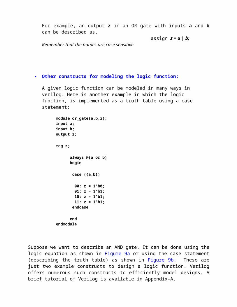
o Assign pin numbers to the input and output pins in the Verilog design file using a “User Constraint File(ucf file)”. The pin numbers can be assigned by looking at section 7 of this tutorial. Then save the design file and implement the design again. Note that you can assign pin numbers only to top-level Verilog file. Then the Project Navigator window looks as shown in Figure 13.

Figure 13 : User Constraint File ( snapshot from Xilinx ISE software)
o For the OR_GATE example, the user constraint file used is as follows:
#Pin 88 and 89 are FPGA pins connected to SW0 and SW1 in the Pegasus Board#Pin 46 of the FPGA is connected to LED0 in the Pegasus Board.
NET a LOC="P88";NET b LOC="P89";NET z LOC="P46";
Click on the Module View, choose the main design file and in the Process View -> User Constraints –> Edit Constraints option, add the user constraint file for the design.
Then, in the Process View window (left-bottom), double click on the ‘Generate Programming file’.
Wait for the programming file to be generated and then click on the “Generate Programming File” -> “Configure Device” option.
Once this is done, the following image pops up. Choose the ‘Select boundary scan’ option and click on NEXT.
Figure 14 : JTAG Programmer window ( snapshot from Xilinx ISE software)

On clicking Next, the following image comes up : Choose the option ‘ Automatically connect to cable and identify device’ and click on Finish.
Figure 15: Boundary-Scan Mode Selection window ( snapshot from Xilinx ISE software)
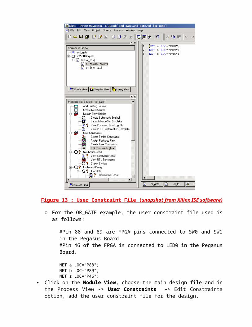
Once this is done, a window pops up where you will see two devices connected in the Boundary scan. The first one xc2s50 is the Spartan FPGA. Right click on the xc2s50 device and select “Assign New configuration file”. Once this is done, click on Ok on the following pop up which will take you to the Select bit file window as shown – Choose or_gate.bit

Now Right click on the xs2s50 device and select program as shown below:

Once you select program, the following window will pop up. Click on OK [There is no need to check the Verify option].
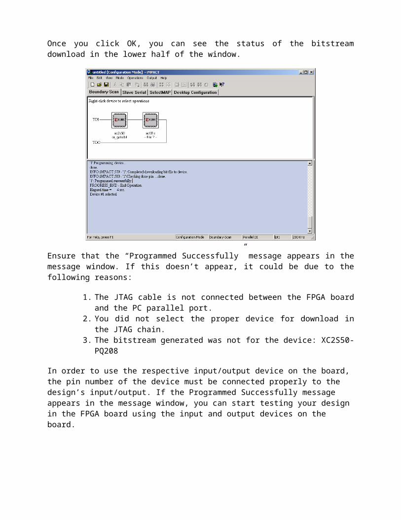
Once you click OK, you can see the status of the bitstream download in the lower half of the window.
Ensure that the “Programmed Successfully” message appears in the message window. If this doesn’t appear, it could be due to the following reasons:
1. The JTAG cable is not connected between the FPGA board and the PC parallel port.
2. You did not select the proper device for download in the JTAG chain.3. The bitstream generated was not for the device: XC2S50-PQ208
In order to use the respective input/output device on the board, the pin number of the device must be connected properly to the design’s input/output. If the Programmed Successfully message appears in the message window, you can start testing your design in the FPGA board using the input and output devices on the board.

7. Testing a Digital Logic Circuit Testing a downloaded design requires connecting the inputs of the design to switches or ports and the outputs of the design to LEDs or 7-segment displays. In case of sequential circuits, the clock input(s) must also be connected to clock sources. These inputs and outputs can be connected to appropriately on the Digital Lab workbench.
The Pegasus Board used in the Digital Circuits lab has the following features which can be used to test the digital logic in the design:
1. 8 Switches -- which can be used to drive upto 8 inputs 2. 4 Buttons -- which can be used as reset signals (or) input switches
3. 8 LEDs -- which can be used to display upto 8 design outputs
4. 4 Seven segment displays -- which can be used to display four digits of information in the display on the board
Figure 16: Pegasus Board Architecture ( Source: www.digitalinc.com)
Outputs Inputs

In order to use the respective input/output device on the board, the pin number of the device must be connected properly to the design’s input/output. In the Pegasus board, the pin number of these inputs/outputs is as follows:
InputFPGA Pin
(To be used in the ucf file)
Switch
SW0 pin# P89 SW1 pin# P88 SW2 pin# P87 SW3 pin# P86 SW4 pin# P84 SW5 pin# P83SW6 pin# P82 SW7 pin# P81
Button
BTN0 pin# P59BTN1 pin# P58BTN2 pin# P57BTN3 pin# P154
InputFPGA Pin
(To be used in the ucf file)
Clock(for sequential designs
GLK1 pin# P77GCLK2 pin# P182
OutputFPGA Pin
(To be used in the ucf file)
LED LD0 pin# P46 LD1 pin# P45 LD2 pin# P44 LD3 pin# P43 LD4 pin# P42 LD5 pin# P41
LD6 pin# P37 LD7 pin# P36
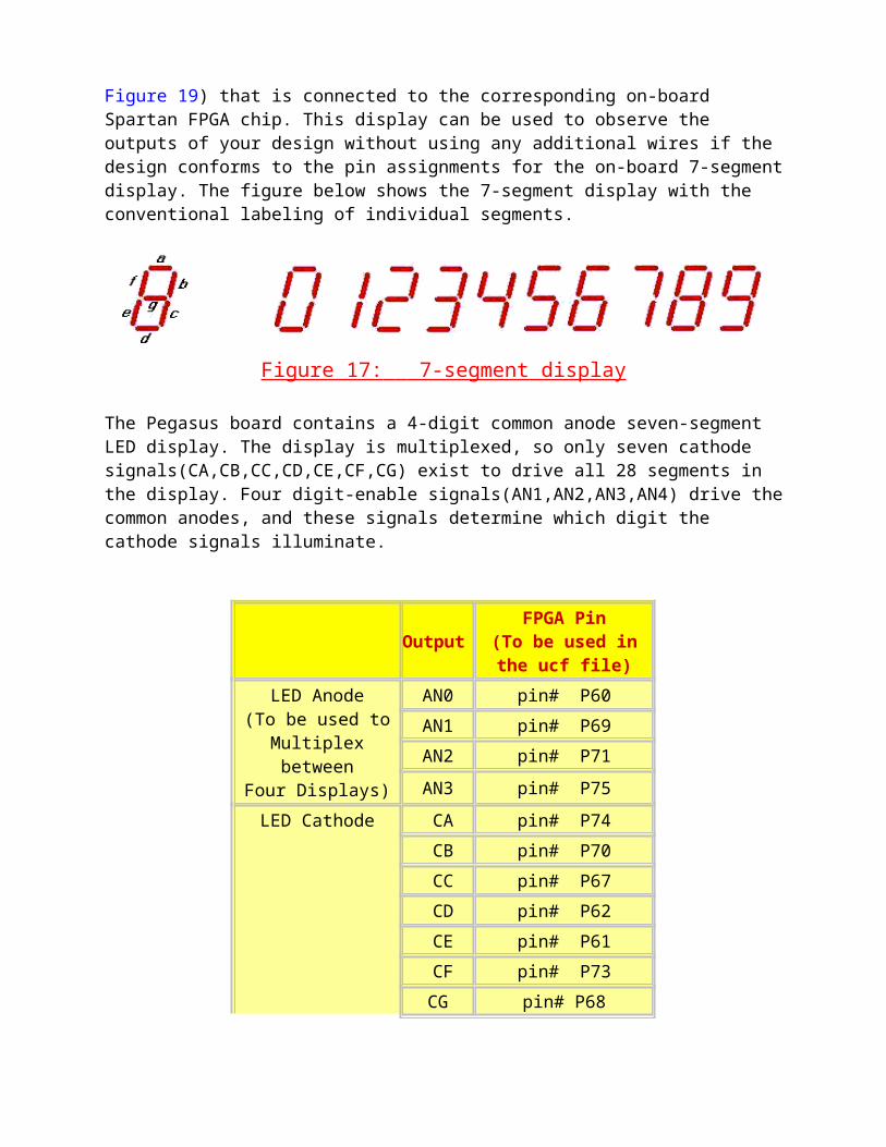
7.1 Observing outputs using the on-board LEDs and Seven Segment Displays The Pegasus boards have four on-board 7-segment display (see Figure 19) that is connected to the corresponding on-board Spartan FPGA chip. This display can be used to observe the outputs of your design without using any additional wires if the design conforms to the pin assignments for the on-board 7-segment display. The figure below shows the 7-segment display with the conventional labeling of individual segments.
Figure 17: 7-segment display
The Pegasus board contains a 4-digit common anode seven-segment LED display. The display is multiplexed, so only seven cathode signals(CA,CB,CC,CD,CE,CF,CG) exist to drive all 28 segments in the display. Four digit-enable signals(AN1,AN2,AN3,AN4) drive the common anodes, and these signals determine which digit the cathode signals illuminate.
OutputFPGA Pin
(To be used in the ucf file)
LED Anode(To be used to
Multiplex betweenFour Displays)
AN0 pin# P60AN1 pin# P69AN2 pin# P71AN3 pin# P75
LED Cathode CA pin# P74 CB pin# P70 CC pin# P67 CD pin# P62 CE pin# P61 CF pin# P73CG pin# P68
This connection scheme creates a multiplexed display, where driving the anode signals and corresponding cathode patterns of each digit in a repeating, continuous succession can create the appearance of a 4-digit display. Each of the four digits will appear bright and continuously

illuminated if the digit enable signals are driven low once every 1 to 16ms (for a refresh frequency of 1KHz to 60Hz).
The Seven segment display timing to drive all the four displays is shown below:
Figure 18: Timing diagram for Multiplexed Seven Segment Displays
8. Design and Simulation of Sequential Circuits using Verilog HDL
The procedure to create Verilog design files for sequential circuits in Xilinx ISE is the same as that for combinational circuits. The main difference between combinational and sequential designs is the presence of flip-flops (registered outputs or nodes in the Declaration section of a sequential design).
8.1 Design of Sequential Circuits For large, complex state machines it is easier to specify them as programs. A sequential circuit can be described either as a procedural block or a state machine in Verilog.
1. A D-flip with asynchronous reset can be modeled as a Procedural block as follows:
module dff_async (data, clock, reset, q); input data, clock, reset; output q;
reg q;
// logic begins here always @(posedge clock or negedge reset) if(reset == 1'b0) q <= 1'b0; else q <= data; endmodule

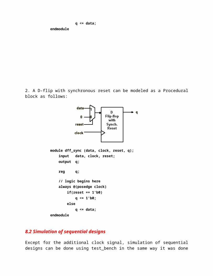
2. A D-flip with synchronous reset can be modeled as a Procedural block as follows:
module dff_sync (data, clock, reset, q); input data, clock, reset; output q;
reg q;
// logic begins here always @(posedge clock) if(reset == 1'b0) q <= 1'b0; else q <= data; endmodule
8.2 Simulation of sequential designs
Except for the additional clock signal, simulation of sequential designs can be done using test_bench in the same way it was done for combinatorial circuits. The clock signal can be generated in the test bench using a simple initial block as follows:
module test_bench(clk)output clk;reg clk;
initial begin clk = 0; forever begin #5 clk = ~clk; //Time period of the clock is 10 time units. end
// rest of the logic
endmodule

9. Hierarchical Circuit Design Using Modules
It is always a good practice to keep a design modular and hierarchical. This is important for designs of moderate to high complexity. [Refer to section on hierarchies and Instantiation in the Verilog tutorial in Appendix-A]. Often, you will use a circuit (module) over and over again. Instead of creating these modules every time you need them, it would be more efficient to make a cell or module out of them. You can then use this module every time to need it by instantiating the module in your circuit. Verilog supports hierarchical design by creating instances of another modules that can be used in a design. In the example depicted in Figure 19, a 4-bit equivalence circuit is designed using 1-bit equivalence circuit modules.
Figure 19: Hierarchical circuit design example: 4-bit equivalence circuit
Module Definition: A module (functional block) definition is specified in a file, separate from the top-level design file using the module.
module equiv (p,q,r)input p;input q;output r;

assign r = ~(p ^ q); //equivalence function is xnor function.
endmodule
Module Usage: A design using a module includes a declaration of module interface and instantiation of each module in the Declaration section. Instantiation of module “equiv” in the 4-bit equivalence circuit shown in Figure.21 can be done as follows:
module equiv4bit(a3,b3,a2,b2,a1,b1,a0,b0,eq4) input a3,b3,a2,b2,a1,b1,a0,b0; output eq4;
equiv eq0(a0,b0,r0); equiv eq1(a1,b1,r1); equiv eq2(a2,b2,r2); equiv eq3(a3,b3,r3);
assign eq4 = r0 & r1 & r2 & r3; endmodule
NOTE : For creation of the module, we can either use the design wizard provided by the Xilinx or create our own.
Appendix-A:
Verilog Hardware Modeling:
This is just an introductory level tutorial to the Verilog language. The reader is encouraged to go through the following Verilog tutorials to understand the language better:
http://www-ee.eng.hawaii.edu/~msmith/ASICs/Files/pdf/CH11.pdf http://www.asic-world.com/verilog/vbehave.html http://www.vol.webnexus.com/ [requires free registration]
1. Module:
A module is the basic building block in Verilog. It is defined as follows: module <module_name> (<portlist>); . . // module components . endmodule
The <module_name> is the type of this module. The <portlist> is the list of connections, or ports, which allows data to flow into and out of modules of this type.
Verilog models are made up of modules. Modules, in turn, are made of different types of components. These include
Parameters Nets Registers Primitives and Instances Continuous Assignments Procedural Blocks Task/Function definitions
2. Ports:
Ports are Verilog structures that pass data between two or more modules. Thus, ports can be thought of as wires connecting modules. The connections provided by ports can be either input, output, or bi-directional (inout).

Module instantiations also contain port lists. This is the means of connecting signals in the parent module with signals in the child module.
3. Nets:
Nets are the things that connect model components together. They are usually thought of as wires in a circuit. Nets are declared in statements like this:
net_type [range] [delay3] list_of_net_identifiers ;
Example:
wire w1, w2; tri [31:0] bus32; wire wire_number_5 = wire_number_2 & wire_number_3;
4. Registers:
Registers are storage elements. Values are stored in registers in procedural assignment statements. Registers can be used as the source for a primitive or module instance (i.e. registers can be connected to input ports), but they cannot be driven in the same way a net can.
Registers are declared in statements like this:
reg [range] list_of_register_identifiers ;
Example:
reg r1, r2; reg [31:0] bus32;

5. Operators in Verilog:
Logical, arithmetic and relational operators available in Verilog are described in Table 1.
Verilog Unary Operators:
Source: ASIC Design by Smith (http://www-ee.eng.hawaii.edu/~msmith/ASICs/Files/pdf/CH11.3.pdf)
Table 1 Verilog Operators
6.. Continuous assignments:
Continuous assignments are sometimes known as data flow statements because they describe how data moves from one place, either a net or register, to another. They are usually thought of as representing combinational logic. In general, any logic functionality which can be
implemented by means of a continuous assignment can also be implemented using primitive instances.
A continuous assignment looks like this:
assign [delay3] list_of_net_assignments ;
Examples:
assign w1 = w2 & w3; assign #1 mynet = enable; // mynet is assigned the value after 1 time unit.
7. Procedural Blocks:
Procedural blocks are the part of the language which represents sequential behavior. A module can have as many procedural blocks as necessary. These blocks are sequences of executable statements. The statements in each block are executed sequentially, but the blocks themselves are concurrent and asynchronous to other blocks.
There are two types of procedural blocks, initial blocks and always blocks.
initial <statement> always <statement>
There may be many initial and always blocks in a module. Since there may be many modules in a model, there may be many initial and always blocks in the entire model. All initial and always blocks contain a single statement, which may be a compound statement, e.g.
initial begin statement1 ; statement2 ; ... end
a. Initial Block:
All initial blocks begin at time 0 and execute the initial statement. Because the statement may be a compound statement, this may entail executing lots of statements. There may be time or event controls, as well as all of the control constructs in the language. As a result, an initial block may cause activity to occur throughout the entire simulation of the model.
When the initial statement finishes execution, the initial block terminates. If the initial statement is a compound statement, then the statement finishes after its last statement finishes.
Example:

initial x = 0; // a simple initialization
initial begin x = 1; // an initialization y = f(x);#1 x = 0; // a value change 1 time unit later y = f(x);end
b. Always Block:
Always blocks also begin at time 0. The only difference between an always block and an initial block is that when the always statement finishes execution, it starts executing again. Note that if there is no time or event control in the always block, simulation time can never advance beyond time 0. Example,
always #10 clock = ~clock;
8. Behavioral modeling constructs:
a. Conditional if-else construct:
The if - else statement controls the execution of other statements in a procedural block. Syntax:
if (condition) statements;
if (condition) statements; else statements; if (condition) statements; else if (condition) statements; ................ ................ else statements;
Example:// Simple if statement if (enable) q <= d;
// One else statement if (reset == 1'b1) q <= 0;; else q <= d;

// Nested if-else-if statements if (reset == 1'b0) counter <= 4'b0000; else if (enable == 1'b1 && up_en == 1'b1) counter <= counter + 1'b1; else if (enable == 1'b1 && down_en == 1'b1); counter <= counter - 1'b0; else counter <= counter; // Redundant code
b. Case statement:
The case statement compares an expression to a series of cases and executes the statement or statement group associated with the first matching case. Case statement supports single or multiple statements. Multiple statements can be grouped using begin and end keywords.
Syntax:
case (<expression>) <case1> : <statement> <case2> : <statement> ..... default : <statement> endcase
Example:
module mux (a,b,c,d,sel,y); input a, b, c, d; input [1:0] sel; output y; reg y; always @ (a or b or c or d or sel) case (sel) 0 : y = a; 1 : y = b; 2 : y = c; 3 : y = d; default : $display("Error in SEL"); endcase endmodule
9. Module instantiations and hierarchies:
Verilog allows you to represent the hierarchy of a design. A more common way of depicting hierarchical relationships is:

We say that a parent instantiates a child module. That is, it creates an instance of it to be a submodel of the parent. In this example,
system instantiates comp_1, comp_2comp_2 instantiates sub_3
Modules in a hierarchy have both a type and a name. Module types are defined in Verilog. There can be many module instances of the same type of module in a single hierarchy. The module definition by itself does not create a module. Modules are created by being instantiated in another module, like this:
module <module_name_1> (<portlist>); . . <module_name_2> <instance_name> (<portlist>); . . endmodule
