msp430tch5e haptics-enabled mixed-signal microcontroller · haptics-enabled mixed-signal...
TRANSCRIPT

MSP430TCH5E
www.ti.com SLAS895 –DECEMBER 2013
Haptics-Enabled Mixed-Signal MicrocontrollerCheck for Samples: MSP430TCH5E
1FEATURES23• Haptics-Enabled Device Authenticated to Run • Universal Serial Communication Interface
Immersion TouchSense™ Technology (USCI)– Supports 122 Different Haptic Effects – Enhanced UART With Automatic Baud Rate
Detection (LIN)– Supports Wide Range of LRA and ERMActuators Offering Maximum Design – IrDA Encoder and DecoderFlexibility – Synchronous SPI
– Highly Customizable Haptics Effects: – I2CMultiple-Effect Sequencing, Delays, and • On-Chip Comparator for Analog SignalRepeat Counters Compare Function or Slope Analog-to-Digital
– Supports Audio Synchronized Haptics (A/D) ConversionPlayout (Audio-to-Haptics) • 10-Bit 200-ksps Analog-to-Digital Converter
– Supports Programmable Solution Allowing (ADC) With Internal Reference, Sample-and-Integration With Capacitive Touch and Hold, and AutoscanOther System Controller Functionality • Brownout Detector
– With Licenses Included • Serial Onboard Programming,• Low Supply-Voltage Range: 1.8 V to 3.6 V No External Programming Voltage Needed,• Ultra-Low-Power Consumption Programmable Code Protection by Security
Fuse– Active Mode: 230 µA at 1 MHz, 2.2 V• On-Chip Emulation Logic With Spy-Bi-Wire– Standby Mode: 0.5 µA
Interface– Off Mode (RAM Retention): 0.1 µA• Family Members are Summarized in Table 1• Five Power-Saving Modes• Available in 28-Pin TSSOP and 32-Pin QFN• Ultra-Fast Wake Up From Standby Mode in
(RHB) PackagesLess Than 1 µs• For Complete Module Descriptions, see the• 16-Bit RISC Architecture, 62.5-ns Instruction
MSP430x2xx Family User’s Guide (SLAU144)Cycle Time• Basic Clock Module Configurations APPLICATIONS
– Internal Frequencies up to 16 MHz With • Touch-Enabled Devices That Require BothFour Calibrated Frequency Capacitive Touch and Haptics Solutions– Internal Very-Low-Power Low-Frequency Integrated
(LF) Oscillator • Portable Gaming Consoles– 32-kHz Crystal • Portable Navigation Devices– External Digital Clock Source • Application Consoles
• Two 16-Bit Timer_A With Three • TabletsCapture/Compare Registers• Mobile Phones• Up to 24 Capacitive Touch I/O Pins
1
Please be aware that an important notice concerning availability, standard warranty, and use in critical applications ofTexas Instruments semiconductor products and disclaimers thereto appears at the end of this data sheet.
2MSP430 is a trademark of Texas Instruments.3TouchSense is a trademark of Immersion Corporation.PRODUCTION DATA information is current as of publication date. Copyright © 2013, Texas Instruments IncorporatedProducts conform to specifications per the terms of the TexasInstruments standard warranty. Production processing does notnecessarily include testing of all parameters.

Haptics and
Capacitive Touch
Controller
MSP430TCH5E
Capacitive Touch
Inputs
DRV2603
Driver
Actuators:
LRA and ERM
DRV Enable
PWM
OUT+
OUT-
Touch-sense
enabled GPIO
MSP430TCH5E
SLAS895 –DECEMBER 2013 www.ti.com
DESCRIPTIONThe MSP430TCH5E device is a haptics-enabled MSP430™ microcontroller that features Immersion TouchSenseTechnology. Haptics technology provides tactile feedback, using mechanical vibrations, dramatically reducinguser error in touch applications. Haptics can be used in a variety of end equipments, including handsets, tablets,digital cameras touch screens, home appliances, computer accessories, automotive products, and more. Hapticscan also be implemented in portable media players to generate subwoofer-like effects using audio-to-hapticstechnology. Haptics is inexpensive to implement and is also a great way to differentiate products. Immersion isthe premier haptics technology provider in the market, and MSP430TCH5E device provides a programmable useof Immersion TouchSense Technology with no additional fees.
The MSP430TCH5E device belongs to the Texas Instruments MSP430 family of ultra-low-powermicrocontrollers, which consists of several devices that feature different sets of peripherals targeted for variousapplications. The architecture, combined with five low-power modes, is optimized to achieve extended battery lifein portable measurement applications. The device features a powerful 16-bit RISC CPU, 16-bit registers, andconstant generators that contribute to maximum code efficiency. The digitally controlled oscillator (DCO) allowsthe device to wake up from low-power modes to active mode in less than 1 µs. Peripherals include 16-bit timers,up to 24 Capacitive Touch I/O pins, a versatile analog comparator, a 10-bit analog-to-digital converter (ADC),and built-in communication capability using the universal serial communication interface (USCI). For configurationdetails, see Table 1.
Capacitive touch buttons are often paired with haptic feedback to improve user experience. The MSP430TCH5Edevice can support capacitive button, slider, and wheel functionality in conjunction with Immersion TouchSenseHaptics Technology. Examples are remote controls, gaming accessories, PC accessories, and control panels onTVs and home appliances.
Typical application configurations include:• Touch-enabled devices where the MSP430TCH5E device is used both as haptics and capacitive touch
controller. See Figure 1.• Host-controlled systems where an external host controls the MSP43TCH5E haptics controller device. See
Figure 2.• Application consoles where the MSP430TCH5E device is used as an Audio-to-Haptics controller that converts
the audio input to respective haptics effects. See Figure 3.
The MSP430TCH5E is not intended for use in Critical Applications. "Critical Application" means a device orapplication where the failure, malfunction, or inaccuracy of the device or application may reasonably be expectedto cause death or severe bodily injury.
Figure 1. Stand-Alone Application With MSP430TCH5E Device as Haptics and Capacitive TouchController
2 Submit Documentation Feedback Copyright © 2013, Texas Instruments Incorporated
Product Folder Links: MSP430TCH5E

Audio-to-Haptics
Controller
MSP430TCH5E
Audio Input
Host Controller
(optional)
DRV2603
Driver
Actuators:
LRA and ERM
DRV Enable
PWM
OUT+
OUT-
I2C
ADC
Input
Haptics Controller
MSP430TCH5E
Host Controller
DRV2603
Driver
Actuators:
LRA and ERM
DRV Enable
PWM
OUT+
OUT-
I2C
MSP430TCH5E
www.ti.com SLAS895 –DECEMBER 2013
Figure 2. Host-Controlled System With an External Host Controlling MSP430TCH5E Device HapticsController
Figure 3. Typical Application Using MSP430TCH5E Device as Audio-to-Haptics Controller
Table 1. Available Options (1) (2)
Flash RAM COMP_A+ ADC10 USCI_A, PackageDevice BSL EEM Timer_A Clock I/O(KB) (B) Channel Channel USCI_B Type
MSP430TCH5ERHB LF, 24 32-QFN1 1 16 512 2x TA3 8 8 1 DCO,
MSP430TCH5EPW 24 28-TSSOPVLO
(1) For the most current package and ordering information, see the Package Option Addendum at the end of this document, or see the TIweb site at www.ti.com.
(2) Package drawings, thermal data, and symbolization are available at www.ti.com/packaging.
Copyright © 2013, Texas Instruments Incorporated Submit Documentation Feedback 3
Product Folder Links: MSP430TCH5E

PW28(TOP VIEW)
1DVCC
2P1.0/TA0CLK/ACLK/A0/CA0
3
4
5P1.3/ADC10CLK/CAOUT/VREF-/VEREF-/A3/CA3
6
7
8
P3.0/TA0.2 9
P3.1/TA1.0
10P2.0/TA1.0 19 P3.5/TA0.1
20 P3.6/TA0.2
21 P3.7/TA1CLK/CAOUT
22
23
24 RST/NMI/SBWTDIO
25 TEST/SBWTCK
26 XOUT/P2.7
27 XIN/P2.6/TA0.1
28 DVSS
P1.6/TA0.1/ CA6/TDI/TCLKUCB0SOMI/UCB0SCL/A6/
P1.7/CAOUT /A7/CA7/TDO/TDI/UCB0SIMO/UCB0SDA
P1.1/TA0.0/ A1/CA1/UCA0RXD/UCA0SOMI
P1.2/TA0.1/ A2/CA2/UCA0TXD/UCA0SIMO
P1.4/SMCLK/ CA4/TCK/VREF+/VEREF+/A4/UCB0STE/UCA0CLK
P1.5/TA0.0/ A5/CA5/TMS/UCB0CLK/UCA0STE
11
12P2.2/TA1.1
13P3.2/TA1.1
14P3.3/TA1.2 15 P3.4/TA0.0
16 P2.3/TA1.0
17 P2.4/TA1.2
18 P2.5/TA1.2P2.1/TA1.1
1
2
3
4
5
6
P2.0
/TA
1.0
7
P2.1
/TA
1.1
8NC9
P2.2
/TA
1.1
10
P3.0/TA0.2
11
P3.1/TA1.0
12
P3.2
/TA
1.1
13P
3.3
/TA
1.2
14
P3.4
/TA
0.0
15
P3.5/TA0.1
16
P2.3
/TA
1.0
17
P2.4
/TA
1.2
18
P2.5/TA1.2
19
20
P3.6/TA0.2
21
P3.7/TA1CLK/CAOUT
22
23 RST/NMI/SBWTDIO
24 TEST/SBWTCK
25
XO
UT
/P2.7
26
XIN
/P2.6
/TA
0.1
27
AV
SS
28
DV
SS
29
AV
CC
30
DV
CC
31
P1.0
/TA
0C
LK
/AC
LK
/A0/C
A0
32
NC
P1.3/ADC10CLK/CAOUT/VREF-/VEREF-/A3/CA3
P1.1/TA0.0/ A1/CA1/UCA0RXD/UCA0SOMI
P1.2/TA0.1/ A2/CA2/UCA0TXD/UCA0SIMO
P1.4/SMCLK/ CA4/TCK/VREF+/VEREF+/A4/UCB0STE/UCA0CLK
P1.5/TA0.0/ A5/CA5/TMS/UCB0CLK/UCA0STE
P1.6/TA0.1/ CA6/TDI/TCLKUCB0SOMI/UCB0SCL/A6/
P1.7/CAOUT /CA7/TDO/TDI/UCB0SIMO/UCB0SDA/A7
MSP430TCH5E
SLAS895 –DECEMBER 2013 www.ti.com
Device Pinout
RHB32 PACKAGE(TOP VIEW)
PW28 PACKAGE(TOP VIEW)
4 Submit Documentation Feedback Copyright © 2013, Texas Instruments Incorporated
Product Folder Links: MSP430TCH5E

ClockSystem
BrownoutProtection
RST/NMI
DVCC DVSS
MCLK
WatchdogWDT+
15-Bit
Timer0_A3
3 CCRegisters
16MHzCPU
incl. 16Registers
Emulation2BP
JTAGInterface
SMCLK
ACLK
MDB
MAB
Port P1
8 I/OInterruptcapability
pullup/downresistors
P1.x
8
P2.x
Port P2
8 I/OInterruptcapability
pullup/downresistors
Spy-Bi-Wire
Comp_A+
8Channels
Timer1_A3
3 CCRegisters
XIN XOUT
Port P3
8 I/O
pullup/pulldownresistors
P3.x
8 8
RAM
512B
Flash
16KB
USCI A0UART/
LIN, IrDA,SPI
USCI B0SPI, I2C
ADC
10-Bit8 Ch.
Autoscan1 ch DMA
MSP430TCH5E
www.ti.com SLAS895 –DECEMBER 2013
Functional Block Diagram
Copyright © 2013, Texas Instruments Incorporated Submit Documentation Feedback 5
Product Folder Links: MSP430TCH5E
MSP430TCH5E
SLAS895 –DECEMBER 2013 www.ti.com
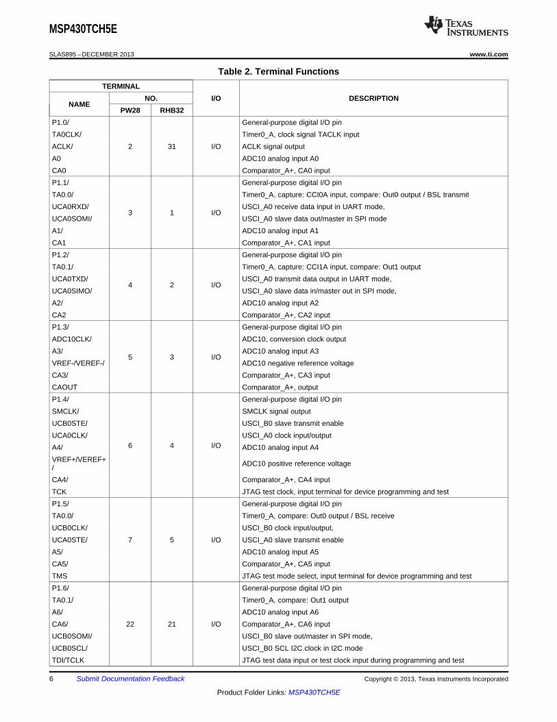
Table 2. Terminal FunctionsTERMINAL
NO. I/O DESCRIPTIONNAME
PW28 RHB32P1.0/ General-purpose digital I/O pinTA0CLK/ Timer0_A, clock signal TACLK inputACLK/ 2 31 I/O ACLK signal outputA0 ADC10 analog input A0CA0 Comparator_A+, CA0 inputP1.1/ General-purpose digital I/O pinTA0.0/ Timer0_A, capture: CCI0A input, compare: Out0 output / BSL transmitUCA0RXD/ USCI_A0 receive data input in UART mode,
3 1 I/OUCA0SOMI/ USCI_A0 slave data out/master in SPI modeA1/ ADC10 analog input A1CA1 Comparator_A+, CA1 inputP1.2/ General-purpose digital I/O pinTA0.1/ Timer0_A, capture: CCI1A input, compare: Out1 outputUCA0TXD/ USCI_A0 transmit data output in UART mode,
4 2 I/OUCA0SIMO/ USCI_A0 slave data in/master out in SPI mode,A2/ ADC10 analog input A2CA2 Comparator_A+, CA2 inputP1.3/ General-purpose digital I/O pinADC10CLK/ ADC10, conversion clock outputA3/ ADC10 analog input A3
5 3 I/OVREF-/VEREF-/ ADC10 negative reference voltageCA3/ Comparator_A+, CA3 inputCAOUT Comparator_A+, outputP1.4/ General-purpose digital I/O pinSMCLK/ SMCLK signal outputUCB0STE/ USCI_B0 slave transmit enableUCA0CLK/ USCI_A0 clock input/output
6 4 I/OA4/ ADC10 analog input A4VREF+/VEREF+ ADC10 positive reference voltage/CA4/ Comparator_A+, CA4 inputTCK JTAG test clock, input terminal for device programming and testP1.5/ General-purpose digital I/O pinTA0.0/ Timer0_A, compare: Out0 output / BSL receiveUCB0CLK/ USCI_B0 clock input/output,UCA0STE/ 7 5 I/O USCI_A0 slave transmit enableA5/ ADC10 analog input A5CA5/ Comparator_A+, CA5 inputTMS JTAG test mode select, input terminal for device programming and testP1.6/ General-purpose digital I/O pinTA0.1/ Timer0_A, compare: Out1 outputA6/ ADC10 analog input A6CA6/ 22 21 I/O Comparator_A+, CA6 inputUCB0SOMI/ USCI_B0 slave out/master in SPI mode,UCB0SCL/ USCI_B0 SCL I2C clock in I2C modeTDI/TCLK JTAG test data input or test clock input during programming and test
6 Submit Documentation Feedback Copyright © 2013, Texas Instruments Incorporated
Product Folder Links: MSP430TCH5E

MSP430TCH5E
www.ti.com SLAS895 –DECEMBER 2013
Table 2. Terminal Functions (continued)TERMINAL
NO. I/O DESCRIPTIONNAME
PW28 RHB32P1.7/ General-purpose digital I/O pinA7/ ADC10 analog input A7CA7/ Comparator_A+, CA7 inputCAOUT/ 23 22 I/O Comparator_A+, outputUCB0SIMO/ USCI_B0 slave in/master out in SPI modeUCB0SDA/ USCI_B0 SDA I2C data in I2C modeTDO/TDI JTAG test data output terminal or test data input during programming and test (1)
P2.0/ General-purpose digital I/O pin10 9 I/O
TA1.0 Timer1_A, capture: CCI0A input, compare: Out0 outputP2.1/ General-purpose digital I/O pin
11 10 I/OTA1.1 Timer1_A, capture: CCI1A input, compare: Out1 outputP2.2/ General-purpose digital I/O pin
12 11 I/OTA1.1 Timer1_A, capture: CCI1B input, compare: Out1 outputP2.3/ General-purpose digital I/O pin
16 15 I/OTA1.0 Timer1_A, capture: CCI0B input, compare: Out0 outputP2.4/ General-purpose digital I/O pin
17 16 I/OTA1.2 Timer1_A, capture: CCI2A input, compare: Out2 outputP2.5/ General-purpose digital I/O pin
18 17 I/OTA1.2 Timer1_A, capture: CCI2B input, compare: Out2 outputXIN/ Input terminal of crystal oscillatorP2.6/ 27 26 I/O General-purpose digital I/O pinTA0.1 Timer0_A, compare: Out1 outputXOUT/ Output terminal of crystal oscillator (2)
26 25 I/OP2.7 General-purpose digital I/O pinP3.0/ General-purpose digital I/O pin
9 7 I/OTA0.2 Timer0_A, capture: CCI2A input, compare: Out2 outputP3.1/ General-purpose digital I/O pin
8 6 I/OTA1.0 Timer1_A, compare: Out0 outputP3.2/ General-purpose digital I/O pin
13 12 I/OTA1.1 Timer1_A, compare: Out1 outputP3.3/ General-purpose digital I/O
14 13 I/OTA1.2 Timer1_A, compare: Out2 outputP3.4/ General-purpose digital I/O
15 14 I/OTA0.0 Timer0_A, compare: Out0 outputP3.5/ General-purpose digital I/O
19 18 I/OTA0.1 Timer0_A, compare: Out1 outputP3.6/ General-purpose digital I/O
20 19 I/OTA0.2 Timer0_A, compare: Out2 outputP3.7/ General-purpose digital I/OTA1CLK/ 21 20 I/O Timer1_A, clock signal TACLK inputCAOUT Comparator_A+, output
(1) TDO or TDI is selected via JTAG instruction.(2) If XOUT/P2.7 is used as an input, excess current flows until P2SEL.7 is cleared. This is due to the oscillator output driver connection to
this pad after reset.
Copyright © 2013, Texas Instruments Incorporated Submit Documentation Feedback 7
Product Folder Links: MSP430TCH5E

MSP430TCH5E
SLAS895 –DECEMBER 2013 www.ti.com
Table 2. Terminal Functions (continued)TERMINAL
NO. I/O DESCRIPTIONNAME
PW28 RHB32RST/ ResetNMI/ 24 23 I Nonmaskable interrupt inputSBWTDIO Spy-Bi-Wire test data input/output during programming and testTEST/ Selects test mode for JTAG pins on Port 1. The device protection fuse is
connected to TEST.25 24 ISBWTCK Spy-Bi-Wire test clock input during programming and testAVCC NA 29 NA Analog supply voltageDVCC 1 30 NA Digital supply voltageDVSS 28 27, 28 NA Ground referenceNC NA 8, 32 NA Not connectedQFN Pad NA Pad NA QFN package pad. Connection to VSS is recommended.
Community ResourcesThe following links connect to TI community resources. Linked contents are provided "AS IS" by the respectivecontributors. They do not constitute TI specifications and do not necessarily reflect TI's views; see TI's Terms ofUse.
TI E2E CommunityTI's Engineer-to-Engineer (E2E) Community. Created to foster collaboration among engineers. At e2e.ti.com, youcan ask questions, share knowledge, explore ideas, and help solve problems with fellow engineers.
TI Embedded Processors WikiTexas Instruments Embedded Processors Wiki. Established to help developers get started with embeddedprocessors from Texas Instruments and to foster innovation and growth of general knowledge about thehardware and software surrounding these devices.
8 Submit Documentation Feedback Copyright © 2013, Texas Instruments Incorporated
Product Folder Links: MSP430TCH5E
Program Counter PC/R0
Stack Pointer SP/R1
Status Register SR/CG1/R2
Constant Generator CG2/R3
General-Purpose Register R4
General-Purpose Register R5
General-Purpose Register R6
General-Purpose Register R7
General-Purpose Register R8
General-Purpose Register R9
General-Purpose Register R10
General-Purpose Register R11
General-Purpose Register R12
General-Purpose Register R13
General-Purpose Register R15
General-Purpose Register R14
MSP430TCH5E
www.ti.com SLAS895 –DECEMBER 2013
Short-Form Description
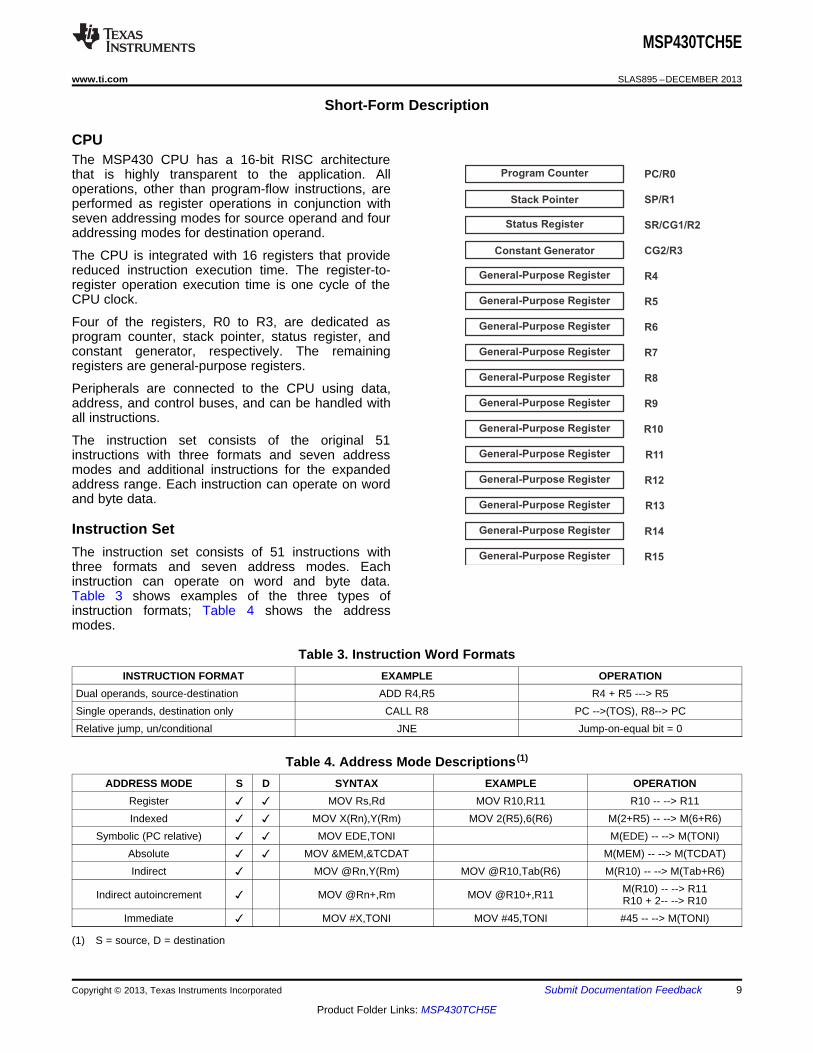
CPUThe MSP430 CPU has a 16-bit RISC architecturethat is highly transparent to the application. Alloperations, other than program-flow instructions, areperformed as register operations in conjunction withseven addressing modes for source operand and fouraddressing modes for destination operand.
The CPU is integrated with 16 registers that providereduced instruction execution time. The register-to-register operation execution time is one cycle of theCPU clock.
Four of the registers, R0 to R3, are dedicated asprogram counter, stack pointer, status register, andconstant generator, respectively. The remainingregisters are general-purpose registers.
Peripherals are connected to the CPU using data,address, and control buses, and can be handled withall instructions.
The instruction set consists of the original 51instructions with three formats and seven addressmodes and additional instructions for the expandedaddress range. Each instruction can operate on wordand byte data.
Instruction SetThe instruction set consists of 51 instructions withthree formats and seven address modes. Eachinstruction can operate on word and byte data.Table 3 shows examples of the three types ofinstruction formats; Table 4 shows the addressmodes.
Table 3. Instruction Word FormatsINSTRUCTION FORMAT EXAMPLE OPERATION
Dual operands, source-destination ADD R4,R5 R4 + R5 ---> R5Single operands, destination only CALL R8 PC -->(TOS), R8--> PCRelative jump, un/conditional JNE Jump-on-equal bit = 0
Table 4. Address Mode Descriptions (1)
ADDRESS MODE S D SYNTAX EXAMPLE OPERATIONRegister MOV Rs,Rd MOV R10,R11 R10 -- --> R11Indexed MOV X(Rn),Y(Rm) MOV 2(R5),6(R6) M(2+R5) -- --> M(6+R6)
Symbolic (PC relative) MOV EDE,TONI M(EDE) -- --> M(TONI)Absolute MOV &MEM,&TCDAT M(MEM) -- --> M(TCDAT)Indirect MOV @Rn,Y(Rm) MOV @R10,Tab(R6) M(R10) -- --> M(Tab+R6)
M(R10) -- --> R11Indirect autoincrement MOV @Rn+,Rm MOV @R10+,R11 R10 + 2-- --> R10Immediate MOV #X,TONI MOV #45,TONI #45 -- --> M(TONI)
(1) S = source, D = destination
Copyright © 2013, Texas Instruments Incorporated Submit Documentation Feedback 9
Product Folder Links: MSP430TCH5E

MSP430TCH5E
SLAS895 –DECEMBER 2013 www.ti.com
Operating ModesThe MSP430 has one active mode and five software selectable low-power modes of operation. An interruptevent can wake up the device from any of the low-power modes, service the request, and restore back to thelow-power mode on return from the interrupt program.
The following six operating modes can be configured by software:• Active mode (AM)
– All clocks are active• Low-power mode 0 (LPM0)
– CPU is disabled– ACLK and SMCLK remain active, MCLK is disabled
• Low-power mode 1 (LPM1)– CPU is disabled– ACLK and SMCLK remain active, MCLK is disabled– DCO's dc generator is disabled if DCO not used in active mode
• Low-power mode 2 (LPM2)– CPU is disabled– MCLK and SMCLK are disabled– DCO's dc generator remains enabled– ACLK remains active
• Low-power mode 3 (LPM3)– CPU is disabled– MCLK and SMCLK are disabled– DCO's dc generator is disabled– ACLK remains active
• Low-power mode 4 (LPM4)– CPU is disabled– ACLK is disabled– MCLK and SMCLK are disabled– DCO's dc generator is disabled– Crystal oscillator is stopped
10 Submit Documentation Feedback Copyright © 2013, Texas Instruments Incorporated
Product Folder Links: MSP430TCH5E

MSP430TCH5E
www.ti.com SLAS895 –DECEMBER 2013
Interrupt Vector AddressesThe interrupt vectors and the power-up starting address are located in the address range 0FFFFh to 0FFC0h.The vector contains the 16-bit address of the appropriate interrupt handler instruction sequence.
If the reset vector (located at address 0FFFEh) contains 0FFFFh (for example, flash is not programmed), theCPU goes into LPM4 immediately after power-up.
Table 5. Interrupt Sources, Flags, and VectorsSYSTEM WORDINTERRUPT SOURCE INTERRUPT FLAG PRIORITYINTERRUPT ADDRESS
Power-Up PORIFGExternal Reset RSTIFG
Watchdog Timer+ WDTIFG Reset 0FFFEh 31, highestFlash key violation KEYV (2)
PC out-of-range (1)
NMI NMIIFG (non)-maskableOscillator fault OFIFG (non)-maskable 0FFFCh 30
Flash memory access violation ACCVIFG (2) (3) (non)-maskableTimer1_A3 TA1CCR0 CCIFG (4) maskable 0FFFAh 29Timer1_A3 TA1CCR2 TA1CCR1 CCIFG, maskable 0FFF8h 28TAIFG (2) (4)
Comparator_A+ CAIFG (4) maskable 0FFF6h 27Watchdog Timer+ WDTIFG maskable 0FFF4h 26
Timer0_A3 TA0CCR0 CCIFG (4) maskable 0FFF2h 25Timer0_A3 TA0CCR2 TA0CCR1 CCIFG, TAIFG maskable 0FFF0h 24(5) (4)
USCI_A0/USCI_B0 receive UCA0RXIFG, UCB0RXIFG (2) (5)maskable 0FFEEh 23USCI_B0 I2C status
USCI_A0/USCI_B0 transmit UCA0TXIFG, UCB0TXIFG (2) (6)maskable 0FFECh 22USCI_B0 I2C receive or transmit
ADC10 ADC10IFG (4) maskable 0FFEAh 210FFE8h 20
I/O Port P2 (up to eight flags) P2IFG.0 to P2IFG.7 (2) (4) maskable 0FFE6h 19I/O Port P1 (up to eight flags) P1IFG.0 to P1IFG.7 (2) (4) maskable 0FFE4h 18
0FFE2h 170FFE0h 16
See (7) 0FFDEh 15See (8) 0FFDEh to 14 to 0, lowest0FFC0h
(1) A reset is generated if the CPU tries to fetch instructions from within the module register memory address range (0h to 01FFh) or fromwithin unused address ranges.
(2) Multiple source flags(3) (non)-maskable: the individual interrupt-enable bit can disable an interrupt event, but the general interrupt enable cannot.(4) Interrupt flags are located in the module.(5) In SPI mode: UCB0RXIFG. In I2C mode: UCALIFG, UCNACKIFG, ICSTTIFG, UCSTPIFG.(6) In UART or SPI mode: UCB0TXIFG. In I2C mode: UCB0RXIFG, UCB0TXIFG.(7) This location is used as bootstrap loader security key (BSLSKEY). A 0xAA55 at this location disables the BSL completely. A zero (0h)
disables the erasure of the flash if an invalid password is supplied.(8) The interrupt vectors at addresses 0FFDEh to 0FFC0h are not used in this device and can be used for regular program code if
necessary.
Copyright © 2013, Texas Instruments Incorporated Submit Documentation Feedback 11
Product Folder Links: MSP430TCH5E

MSP430TCH5E
SLAS895 –DECEMBER 2013 www.ti.com
Special Function Registers (SFRs)Most interrupt and module enable bits are collected into the lowest address space. Special function register bitsnot allocated to a functional purpose are not physically present in the device. Simple software access is providedwith this arrangement.
Legend rw: Bit can be read and written.rw-0,1: Bit can be read and written. It is reset or set by PUC.rw-(0,1): Bit can be read and written. It is reset or set by POR.
SFR bit is not present in device.
Table 6. Interrupt Enable Register 1 and 2Address 7 6 5 4 3 2 1 0
00h ACCVIE NMIIE OFIE WDTIErw-0 rw-0 rw-0 rw-0
WDTIE Watchdog Timer interrupt enable. Inactive if watchdog mode is selected. Active if Watchdog Timer is configured ininterval timer mode.
OFIE Oscillator fault interrupt enableNMIIE (Non)maskable interrupt enableACCVIE Flash access violation interrupt enable
Address 7 6 5 4 3 2 1 001h UCB0TXIE UCB0RXIE UCA0TXIE UCA0RXIE
rw-0 rw-0 rw-0 rw-0
UCA0RXIE USCI_A0 receive interrupt enableUCA0TXIE USCI_A0 transmit interrupt enableUCB0RXIE USCI_B0 receive interrupt enableUCB0TXIE USCI_B0 transmit interrupt enable
Table 7. Interrupt Flag Register 1 and 2Address 7 6 5 4 3 2 1 0
02h NMIIFG RSTIFG PORIFG OFIFG WDTIFGrw-0 rw-(0) rw-(1) rw-1 rw-(0)
WDTIFG Set on watchdog timer overflow (in watchdog mode) or security key violation.Reset on VCC power-on or a reset condition at the RST/NMI pin in reset mode.
OFIFG Flag set on oscillator fault.PORIFG Power-On Reset interrupt flag. Set on VCC power-up.RSTIFG External reset interrupt flag. Set on a reset condition at RST/NMI pin in reset mode. Reset on VCC power-up.NMIIFG Set via RST/NMI pin
Address 7 6 5 4 3 2 1 003h UCB0TXIFG UCB0RXIFG UCA0TXIFG UCA0RXIFG
rw-1 rw-0 rw-1 rw-0
UCA0RXIFG USCI_A0 receive interrupt flagUCA0TXIFG USCI_A0 transmit interrupt flagUCB0RXIFG USCI_B0 receive interrupt flagUCB0TXIFG USCI_B0 transmit interrupt flag
12 Submit Documentation Feedback Copyright © 2013, Texas Instruments Incorporated
Product Folder Links: MSP430TCH5E

MSP430TCH5E
www.ti.com SLAS895 –DECEMBER 2013
Memory Organization
Table 8. Memory Organization
MSP430TCH5E
Memory Size 16kB
Main: interrupt vector Flash 0xFFFF to 0xFFC0
Main: code memory Flash 0xFFFF to 0xC000
Information memory Size 256 Byte
Flash 010FFh to 01000h
RAM Size 512 Byte
0x03FF to 0x0200
Peripherals 16-bit 01FFh to 0100h
8-bit 0FFh to 010h
8-bit SFR 0Fh to 00h
Bootstrap Loader (BSL)The MSP430 BSL enables users to program the flash memory or RAM using a UART serial interface. Access tothe MSP430 memory via the BSL is protected by user-defined password. For complete description of thefeatures of the BSL and its implementation, see the MSP430 Programming Via the Bootstrap Loader User'sGuide (SLAU319).
Table 9. BSL Function PinsBSL FUNCTION 28-PIN PW PACKAGE 32-PIN RHB PACKAGE
Data transmit 3 - P1.1 1 - P1.1Data receive 7 - P1.5 5 - P1.5
Flash MemoryThe flash memory can be programmed via the Spy-Bi-Wire/JTAG port or in-system by the CPU. The CPU canperform single-byte and single-word writes to the flash memory. Features of the flash memory include:• Flash memory has n segments of main memory and four segments of information memory (A to D) of
64 bytes each. Each segment in main memory is 512 bytes in size.• Segments 0 to n may be erased in one step, or each segment may be individually erased.• Segments A to D can be erased individually or as a group with segments 0 to n. Segments A to D are also
called information memory.• Segment A contains calibration data. After reset segment A is protected against programming and erasing. It
can be unlocked but care should be taken not to erase this segment if the device-specific calibration data isrequired.
Copyright © 2013, Texas Instruments Incorporated Submit Documentation Feedback 13
Product Folder Links: MSP430TCH5E

DCO(RSEL,DCO+1)DCO(RSEL,DCO)average
DCO(RSEL,DCO) DCO(RSEL,DCO+1)
32 × f × ff =
MOD × f + (32 – MOD) × f
MSP430TCH5E
SLAS895 –DECEMBER 2013 www.ti.com
PeripheralsPeripherals are connected to the CPU through data, address, and control buses and can be handled using allinstructions. For complete module descriptions, see the MSP430x2xx Family User's Guide (SLAU144).
Oscillator and System ClockThe clock system is supported by the basic clock module that includes support for a 32768-Hz watch crystaloscillator, an internal very-low-power low-frequency oscillator and an internal digitally controlled oscillator (DCO).The basic clock module is designed to meet the requirements of both low system cost and low powerconsumption. The internal DCO provides a fast turn-on clock source and stabilizes in less than 1 µs. The basicclock module provides the following clock signals:• Auxiliary clock (ACLK), sourced either from a 32768-Hz watch crystal or the internal LF oscillator.• Main clock (MCLK), the system clock used by the CPU.• Sub-Main clock (SMCLK), the sub-system clock used by the peripheral modules.
The DCO settings to calibrate the DCO output frequency are stored in the information memory segment A.
Main DCO Characteristics• All ranges selected by RSELx overlap with RSELx + 1: RSELx = 0 overlaps RSELx = 1, ... RSELx = 14
overlaps RSELx = 15.• DCO control bits DCOx have a step size as defined by parameter SDCO.• Modulation control bits MODx select how often fDCO(RSEL,DCO+1) is used within the period of 32 DCOCLK
cycles. The frequency fDCO(RSEL,DCO) is used for the remaining cycles. The frequency is an average equal to:
14 Submit Documentation Feedback Copyright © 2013, Texas Instruments Incorporated
Product Folder Links: MSP430TCH5E

MSP430TCH5E
www.ti.com SLAS895 –DECEMBER 2013
Calibration Data Stored in Information Memory Segment ACalibration data is stored for both the DCO and for ADC10 organized in a tag-length-value structure.
Table 10. Tags Used by the ADC Calibration TagsNAME ADDRESS VALUE DESCRIPTION
TAG_DCO_30 0x10F6 0x01 DCO frequency calibration at VCC = 3 V and TA = 30°C at calibrationTAG_ADC10_1 0x10DA 0x10 ADC10_1 calibration tagTAG_EMPTY - 0xFE Identifier for empty memory areas
Table 11. Labels Used by the ADC Calibration TagsADDRESSLABEL SIZE CONDITION AT CALIBRATION / DESCRIPTIONOFFSET
CAL_ADC_25T85 0x0010 word INCHx = 0x1010, REF2_5 = 1, TA = 85°CCAL_ADC_25T30 0x000E word INCHx = 0x1010, REF2_5 = 1, TA = 30°C
CAL_ADC_25VREF_FACTOR 0x000C word REF2_5 = 1, TA = 30°C, IVREF+ = 1 mACAL_ADC_15T85 0x000A word INCHx = 0x1010, REF2_5 = 0, TA = 85°CCAL_ADC_15T30 0x0008 word INCHx = 0x1010, REF2_5 = 0, TA = 30°C
CAL_ADC_15VREF_FACTOR 0x0006 word REF2_5 = 0, TA = 30°C, IVREF+ = 0.5 mACAL_ADC_OFFSET 0x0004 word External VREF = 1.5 V, fADC10CLK = 5 MHz
CAL_ADC_GAIN_FACTOR 0x0002 word External VREF = 1.5 V, fADC10CLK = 5 MHzCAL_BC1_1MHZ 0x0009 byte -CAL_DCO_1MHZ 0x0008 byte -CAL_BC1_8MHZ 0x0007 byte -CAL_DCO_8MHZ 0x0006 byte -CAL_BC1_12MHZ 0x0005 byte -CAL_DCO_12MHZ 0x0004 byte -CAL_BC1_16MHZ 0x0003 byte -CAL_DCO_16MHZ 0x0002 byte -
BrownoutThe brownout circuit is implemented to provide the proper internal reset signal to the device during power on andpower off.
Digital I/OUp to three 8-bit I/O ports are implemented:• All individual I/O bits are independently programmable.• Any combination of input, output, and interrupt condition (port P1 and port P2 only) is possible.• Edge-selectable interrupt input capability for all bits of port P1 and port P2 (if available).• Read/write access to port-control registers is supported by all instructions.• Each I/O has an individually programmable pullup/pulldown resistor.• Each I/O has an individually programmable pin oscillator enable bit to enable low-cost capacitive touch
sensing.
WDT+ Watchdog TimerThe primary function of the watchdog timer (WDT+) module is to perform a controlled system restart after asoftware problem occurs. If the selected time interval expires, a system reset is generated. If the watchdogfunction is not needed in an application, the module can be disabled or configured as an interval timer and cangenerate interrupts at selected time intervals.
Copyright © 2013, Texas Instruments Incorporated Submit Documentation Feedback 15
Product Folder Links: MSP430TCH5E

MSP430TCH5E
SLAS895 –DECEMBER 2013 www.ti.com
Timer_A3 (TA0, TA1)Timer0/1_A3 is a 16-bit timer/counter with three capture/compare registers. Timer_A3 can support multiplecapture/compares, PWM outputs, and interval timing. Timer_A3 also has extensive interrupt capabilities.Interrupts may be generated from the counter on overflow conditions and from each of the capture/compareregisters.
Table 12. Timer0_A3 Signal ConnectionsINPUT PIN NUMBER MODULE OUTPUT PIN NUMBERDEVICE INPUT MODULE MODULE OUTPUTSIGNAL INPUT NAME BLOCKPW28 RHB32 PW28 RHB32SIGNAL
P1.0-2 P1.0-31 TACLK TACLKACLK ACLK
Timer NASMCLK SMCLK
PinOsc PinOsc TACLK INCLKP1.1-3 P1.1-1 TA0.0 CCI0A P1.1-3 P1.1-1
ACLK CCI0B P1.5-7 P1.5-5CCR0 TA0
VSS GND P3.4-15 P3.4-14VCC VCC
P1.2-4 P1.2-2 TA0.1 CCI1A P1.2-4 P1.2-2CAOUT CCI1B P1.6-22 P1.6-21
CCR1 TA1VSS GND P2.6-27 P2.6-26VCC VCC P3.5-19 P3.5-18
P3.0-9 P3.0-7 TA0.2 CCI2A P3.0-9 P3.0-7PinOsc PinOsc TA0.2 CCI2B P3.6-20 P3.6-19
CCR2 TA2VSS GNDVCC VCC
Table 13. Timer1_A3 Signal ConnectionsINPUT PIN NUMBER MODULE OUTPUT PIN NUMBERDEVICE INPUT MODULE MODULE OUTPUTSIGNAL INPUT NAME BLOCKPW28 RHB32 PW28 RHB32SIGNAL
P3.7-21 P3.7-20 TACLK TACLKACLK ACLK
Timer NASMCLK SMCLK
P3.7-21 P3.7-20 TACLK INCLKP2.0-10 P2.0-9 TA1.0 CCI0A P2.0-10 P2.0-9P2.3-16 P2.3-12 TA1.0 CCI0B P2.3-16 P2.3-15
CCR0 TA0VSS GND P3.1-8 P3.1-6VCC VCC
P2.1-11 P2.1-10 TA1.1 CCI1A P2.1-11 P2.1-10P2.2-12 P2.2-11 TA1.1 CCI1B P2.2-12 P2.2-11
CCR1 TA1VSS GND P3.2-13 P3.2-12VCC VCC
P2.4-17 P2.4-16 TA1.2 CCI2A P2.4-17 P2.4-16P2.5-18 P2.5-17 TA1.2 CCI2B P2.5-18 P2.5-17
CCR2 TA2VSS GND P3.3-14 P3.3-13VCC VCC
16 Submit Documentation Feedback Copyright © 2013, Texas Instruments Incorporated
Product Folder Links: MSP430TCH5E

MSP430TCH5E
www.ti.com SLAS895 –DECEMBER 2013
Universal Serial Communications Interface (USCI)The USCI module is used for serial data communication. The USCI module supports synchronouscommunication protocols such as SPI (3 or 4 pin) and I2C, and asynchronous communication protocols such asUART, enhanced UART with automatic baudrate detection (LIN), and IrDA. Not all packages support the USCIfunctionality.
USCI_A0 provides support for SPI (3 or 4 pin), UART, enhanced UART, and IrDA.
USCI_B0 provides support for SPI (3 or 4 pin) and I2C.
Comparator_A+The primary function of the comparator_A+ module is to support precision slope analog-to-digital conversions,battery-voltage supervision, and monitoring of external analog signals.
ADC10The ADC10 module supports fast 10-bit analog-to-digital conversions. The module implements a 10-bit SARcore, sample select control, reference generator, and data transfer controller (DTC) for automatic conversionresult handling, allowing ADC samples to be converted and stored without any CPU intervention.
Haptics Enabled DeviceThe MSP430TCH5E is accompanied by TI’s MSP430 Haptics Library (SLAU543), which incorporates ImmersionTouchSense Technology. It includes 122 different haptics effects and is highly customizable to do multi-effectsequencing, delays, and repeat counters, resulting in an almost infinite and varied range of possibilities. A widerange of Eccentric Rotating Mass (ERM) and Linear Resonant Actuators (LRA) can be used with the library. Thelibrary also includes an audio-to-haptics feature, which creates a rich haptics experience based on an audioinput.
The library has both an API interface for integrated applications and an I2C command protocol, which allows theMSP430TCH5E to serve as a stand-alone haptics device with minimal development effort. A common exampleof functionality that can be integrated is capacitive touch buttons, sliders, or wheels. This is easily accomplishedby pairing the Haptics Library with TI’s Capacitive Touch Library (SLAA490). The MSP430 Haptics Libraryincludes examples to assist in these applications.
Copyright © 2013, Texas Instruments Incorporated Submit Documentation Feedback 17
Product Folder Links: MSP430TCH5E
MSP430TCH5E
SLAS895 –DECEMBER 2013 www.ti.com
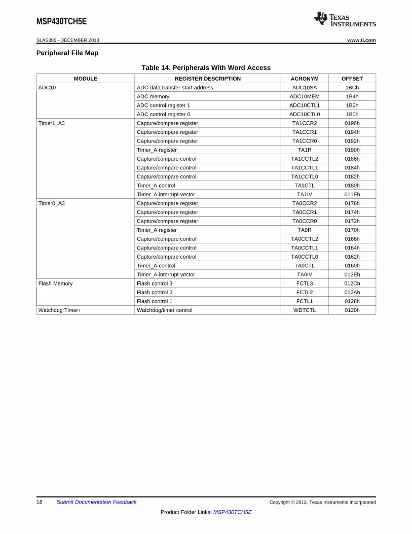
Peripheral File Map
Table 14. Peripherals With Word AccessMODULE REGISTER DESCRIPTION ACRONYM OFFSET
ADC10 ADC data transfer start address ADC10SA 1BChADC memory ADC10MEM 1B4hADC control register 1 ADC10CTL1 1B2hADC control register 0 ADC10CTL0 1B0h
Timer1_A3 Capture/compare register TA1CCR2 0196hCapture/compare register TA1CCR1 0194hCapture/compare register TA1CCR0 0192hTimer_A register TA1R 0190hCapture/compare control TA1CCTL2 0186hCapture/compare control TA1CCTL1 0184hCapture/compare control TA1CCTL0 0182hTimer_A control TA1CTL 0180hTimer_A interrupt vector TA1IV 011Eh
Timer0_A3 Capture/compare register TA0CCR2 0176hCapture/compare register TA0CCR1 0174hCapture/compare register TA0CCR0 0172hTimer_A register TA0R 0170hCapture/compare control TA0CCTL2 0166hCapture/compare control TA0CCTL1 0164hCapture/compare control TA0CCTL0 0162hTimer_A control TA0CTL 0160hTimer_A interrupt vector TA0IV 012Eh
Flash Memory Flash control 3 FCTL3 012ChFlash control 2 FCTL2 012AhFlash control 1 FCTL1 0128h
Watchdog Timer+ Watchdog/timer control WDTCTL 0120h
18 Submit Documentation Feedback Copyright © 2013, Texas Instruments Incorporated
Product Folder Links: MSP430TCH5E

MSP430TCH5E
www.ti.com SLAS895 –DECEMBER 2013
Table 15. Peripherals With Byte AccessMODULE REGISTER DESCRIPTION ACRONYM OFFSET
USCI_B0 USCI_B0 transmit buffer UCB0TXBUF 06FhUSCI_B0 receive buffer UCB0RXBUF 06EhUSCI_B0 status UCB0STAT 06DhUSCI B0 I2C Interrupt enable UCB0CIE 06ChUSCI_B0 bit rate control 1 UCB0BR1 06BhUSCI_B0 bit rate control 0 UCB0BR0 06AhUSCI_B0 control 1 UCB0CTL1 069hUSCI_B0 control 0 UCB0CTL0 068hUSCI_B0 I2C slave address UCB0SA 011AhUSCI_B0 I2C own address UCB0OA 0118h
USCI_A0 USCI_A0 transmit buffer UCA0TXBUF 067hUSCI_A0 receive buffer UCA0RXBUF 066hUSCI_A0 status UCA0STAT 065hUSCI_A0 modulation control UCA0MCTL 064hUSCI_A0 baud rate control 1 UCA0BR1 063hUSCI_A0 baud rate control 0 UCA0BR0 062hUSCI_A0 control 1 UCA0CTL1 061hUSCI_A0 control 0 UCA0CTL0 060hUSCI_A0 IrDA receive control UCA0IRRCTL 05FhUSCI_A0 IrDA transmit control UCA0IRTCTL 05EhUSCI_A0 auto baud rate control UCA0ABCTL 05Dh
ADC10 ADC analog enable 0 ADC10AE0 04AhADC analog enable 1 ADC10AE1 04BhADC data transfer control register 1 ADC10DTC1 049hADC data transfer control register 0 ADC10DTC0 048h
Comparator_A+ Comparator_A+ port disable CAPD 05BhComparator_A+ control 2 CACTL2 05AhComparator_A+ control 1 CACTL1 059h
Basic Clock System+ Basic clock system control 3 BCSCTL3 053hBasic clock system control 2 BCSCTL2 058hBasic clock system control 1 BCSCTL1 057hDCO clock frequency control DCOCTL 056h
Port P3 Port P3 selection 2 P3SEL2 043hPort P3 resistor enable P3REN 010hPort P3 selection P3SEL 01BhPort P3 direction P3DIR 01AhPort P3 output P3OUT 019hPort P3 input P3IN 018h
Port P2 Port P2 selection 2 P2SEL2 042hPort P2 resistor enable P2REN 02FhPort P2 selection P2SEL 02EhPort P2 interrupt enable P2IE 02DhPort P2 interrupt edge select P2IES 02ChPort P2 interrupt flag P2IFG 02BhPort P2 direction P2DIR 02AhPort P2 output P2OUT 029hPort P2 input P2IN 028h
Copyright © 2013, Texas Instruments Incorporated Submit Documentation Feedback 19
Product Folder Links: MSP430TCH5E

MSP430TCH5E
SLAS895 –DECEMBER 2013 www.ti.com
Table 15. Peripherals With Byte Access (continued)MODULE REGISTER DESCRIPTION ACRONYM OFFSET
Port P1 Port P1 selection 2 P1SEL2 041hPort P1 resistor enable P1REN 027hPort P1 selection P1SEL 026hPort P1 interrupt enable P1IE 025hPort P1 interrupt edge select P1IES 024hPort P1 interrupt flag P1IFG 023hPort P1 direction P1DIR 022hPort P1 output P1OUT 021hPort P1 input P1IN 020h
Special Function SFR interrupt flag 2 IFG2 003hSFR interrupt flag 1 IFG1 002hSFR interrupt enable 2 IE2 001hSFR interrupt enable 1 IE1 000h
20 Submit Documentation Feedback Copyright © 2013, Texas Instruments Incorporated
Product Folder Links: MSP430TCH5E

Supply voltage rangeduring flash memoryprogramming
Supply voltage rangeduring program execution
Legend:16 MHz
Syste
m F
requency -
MH
z
12 MHz
6 MHz
1.8 V
Supply Voltage - V
3.3 V2.7 V2.2 V 3.6 V
MSP430TCH5E
www.ti.com SLAS895 –DECEMBER 2013
Absolute Maximum Ratings (1)
Voltage applied at VCC to VSS –0.3 V to 4.1 VVoltage applied to any pin (2) –0.3 V to VCC + 0.3 VDiode current at any device pin ±2 mA
Unprogrammed device –55°C to 150°CStorage temperature range, Tstg
(3)Programmed device –55°C to 150°C
(1) Stresses beyond those listed under "absolute maximum ratings" may cause permanent damage to the device. These are stress ratingsonly, and functional operation of the device at these or any other conditions beyond those indicated under "recommended operatingconditions" is not implied. Exposure to absolute-maximum-rated conditions for extended periods may affect device reliability.
(2) All voltages referenced to VSS. The JTAG fuse-blow voltage, VFB, is allowed to exceed the absolute maximum rating. The voltage isapplied to the TEST pin when blowing the JTAG fuse.
(3) Higher temperature may be applied during board soldering according to the current JEDEC J-STD-020 specification with peak reflowtemperatures not higher than classified on the device label on the shipping boxes or reels.
Recommended Operating ConditionsTypical values are specified at VCC = 3.3 V and TA = 25°C (unless otherwise noted)
MIN NOM MAX UNITDuring program execution 1.8 3.6
VCC Supply voltage VDuring flash programming 2.2 3.6or eraseVSS Supply voltage 0 VTA Operating free-air temperature –40 85 °C
VCC = 1.8 V, dc 6Duty cycle = 50% ± 10%Processor frequency (maximum MCLK frequency using the VCC = 2.7 V,fSYSTEM dc 12 MHzUSART module) (1) (2) Duty cycle = 50% ± 10%
VCC = 3.3 V, dc 16Duty cycle = 50% ± 10%
(1) The MSP430 CPU is clocked directly with MCLK. Both the high and low phase of MCLK must not exceed the pulse duration of thespecified maximum frequency.
(2) Modules might have a different maximum input clock specification. See the specification of the respective module in this data sheet.
Note: Minimum processor frequency is defined by system clock. Flash program or erase operations require a minimum VCCof 2.2 V.
Figure 4. Safe Operating Area
Copyright © 2013, Texas Instruments Incorporated Submit Documentation Feedback 21
Product Folder Links: MSP430TCH5E

0.0
1.0
2.0
3.0
4.0
5.0
1.5 2.0 2.5 3.0 3.5 4.0
VCC − Supply Voltage − V
Active
Mo
de
Cu
rre
nt
−m
A
fDCO = 1 MHz
fDCO = 8 MHz
fDCO = 12 MHz
fDCO = 16 MHz
0.0
1.0
2.0
3.0
4.0
0.0 4.0 8.0 12.0 16.0
fDCO − DCO Frequency − MHz
Active M
ode C
urr
ent
−m
A
TA = 25 °C
TA = 85 °C
VCC = 2.2 V
VCC = 3 V
TA = 25 °C
TA = 85 °C
MSP430TCH5E
SLAS895 –DECEMBER 2013 www.ti.com
Electrical Characteristics
Active Mode Supply Current Into VCC Excluding External Currentover recommended ranges of supply voltage and operating free-air temperature (unless otherwise noted) (1) (2)
PARAMETER TEST CONDITIONS VCC MIN TYP MAX UNITfDCO = fMCLK = fSMCLK = 1 MHz, 2.2 V 230fACLK = 0 Hz,Program executes in flash,Active mode (AM)IAM,1MHz BCSCTL1 = CALBC1_1MHZ, µAcurrent at 1 MHz 3 V 330 420DCOCTL = CALDCO_1MHZ,CPUOFF = 0, SCG0 = 0, SCG1 = 0,OSCOFF = 0
(1) All inputs are tied to 0 V or to VCC. Outputs do not source or sink any current.(2) The currents are characterized with a Micro Crystal CC4V-T1A SMD crystal with a load capacitance of 9 pF. The internal and external
load capacitance is chosen to closely match the required 9 pF.
Typical Characteristics, Active Mode Supply Current (Into VCC)
Figure 5. Active Mode Current vs VCC, TA = 25°C Figure 6. Active Mode Current vs DCO Frequency
22 Submit Documentation Feedback Copyright © 2013, Texas Instruments Incorporated
Product Folder Links: MSP430TCH5E

0.00
0.25
0.50
0.75
1.00
1.25
1.50
1.75
2.00
2.25
2.50
2.75
3.00
-40
I–
Lo
w-P
ow
er
Mo
de C
urr
en
t–
µA
LP
M3
Vcc = 3.6 V
T – Temperature – °CA
Vcc = 1.8 V
Vcc = 3 V
Vcc = 2.2 V
-20 0 20 40 60 80
0.00
0.25
0.50
0.75
1.00
1.25
1.50
1.75
2.00
2.25
2.50
-40
I–
Lo
w-P
ow
er
Mo
de C
urr
en
t–
µA
LP
M4
Vcc = 3.6 V
T – Temperature – °CA
Vcc = 1.8 V
Vcc = 3 V
Vcc = 2.2 V
-20 0 20 40 60 80
MSP430TCH5E
www.ti.com SLAS895 –DECEMBER 2013
Low-Power Mode Supply Currents (Into VCC) Excluding External Currentover recommended ranges of supply voltage and operating free-air temperature (unless otherwise noted) (1) (2)
PARAMETER TEST CONDITIONS TA VCC MIN TYP MAX UNITfMCLK = 0 MHz,fSMCLK = fDCO = 1 MHz,fACLK = 32768 Hz,Low-power mode 0ILPM0,1MHz BCSCTL1 = CALBC1_1MHZ, 25°C 2.2 V 56 µA(LPM0) current (3)DCOCTL = CALDCO_1MHZ,CPUOFF = 1, SCG0 = 0, SCG1 = 0,OSCOFF = 0fMCLK = fSMCLK = 0 MHz,fDCO = 1 MHz,fACLK = 32768 Hz,Low-power mode 2ILPM2 BCSCTL1 = CALBC1_1MHZ, 25°C 2.2 V 22 µA(LPM2) current (4)DCOCTL = CALDCO_1MHZ,CPUOFF = 1, SCG0 = 0, SCG1 = 1,OSCOFF = 0fDCO = fMCLK = fSMCLK = 0 MHz,
Low-power mode 3 fACLK = 32768 Hz,ILPM3,LFXT1 25°C 2.2 V 0.7 1.5 µA(LPM3) current (4) CPUOFF = 1, SCG0 = 1, SCG1 = 1,OSCOFF = 0fDCO = fMCLK = fSMCLK = 0 MHz,
Low-power mode 3 fACLK from internal LF oscillator (VLO),ILPM3,VLO 25°C 2.2 V 0.5 0.7 µAcurrent, (LPM3) (4) CPUOFF = 1, SCG0 = 1, SCG1 = 1,OSCOFF = 0fDCO = fMCLK = fSMCLK = 0 MHz, 25°C 0.1 0.5
Low-power mode 4 fACLK = 0 Hz,ILPM4 2.2 V µA(LPM4) current (5) CPUOFF = 1, SCG0 = 1, SCG1 = 1, 85°C 0.8 1.7OSCOFF = 1
(1) All inputs are tied to 0 V or to VCC. Outputs do not source or sink any current.(2) The currents are characterized with a Micro Crystal CC4V-T1A SMD crystal with a load capacitance of 9 pF. The internal and external
load capacitance is chosen to closely match the required 9 pF.(3) Current for brownout and WDT clocked by SMCLK included.(4) Current for brownout and WDT clocked by ACLK included.(5) Current for brownout included.
Typical Characteristics, Low-Power Mode Supply Currentsover recommended ranges of supply voltage and operating free-air temperature (unless otherwise noted)
Figure 7. LPM3 Current vs Temperature Figure 8. LPM4 Current vs Temperature
Copyright © 2013, Texas Instruments Incorporated Submit Documentation Feedback 23
Product Folder Links: MSP430TCH5E

MSP430TCH5E
SLAS895 –DECEMBER 2013 www.ti.com
Schmitt-Trigger Inputs, Ports Pxover recommended ranges of supply voltage and operating free-air temperature (unless otherwise noted)
PARAMETER TEST CONDITIONS VCC MIN TYP MAX UNIT0.45 VCC 0.75 VCCVIT+ Positive-going input threshold voltage V
3 V 1.35 2.250.25 VCC 0.55 VCCVIT– Negative-going input threshold voltage V
3 V 0.75 1.65Vhys Input voltage hysteresis (VIT+ – VIT–) 3 V 0.3 1 V
For pullup: VIN = VSSRPull Pullup or pulldown resistor 3 V 20 35 50 kΩFor pulldown: VIN = VCC
CI Input capacitance VIN = VSS or VCC 5 pF
Leakage Current, Ports Pxover recommended ranges of supply voltage and operating free-air temperature (unless otherwise noted)
PARAMETER TEST CONDITIONS VCC MIN MAX UNITIlkg(Px.y) High-impedance leakage current (1) (2) 3 V ±50 nA
(1) The leakage current is measured with VSS or VCC applied to the corresponding pin(s), unless otherwise noted.(2) The leakage of the digital port pins is measured individually. The port pin is selected for input and the pullup/pulldown resistor is
disabled.
Outputs, Ports Pxover recommended ranges of supply voltage and operating free-air temperature (unless otherwise noted)
PARAMETER TEST CONDITIONS VCC MIN TYP MAX UNITVOH High-level output voltage I(OHmax) = –6 mA (1) 3 V VCC – 0.3 VVOL Low-level output voltage I(OLmax) = 6 mA (1) 3 V VSS + 0.3 V
(1) The maximum total current, I(OHmax) and I(OLmax), for all outputs combined should not exceed ±48 mA to hold the maximum voltage dropspecified.
Output Frequency, Ports Pxover recommended ranges of supply voltage and operating free-air temperature (unless otherwise noted)
PARAMETER TEST CONDITIONS VCC MIN TYP MAX UNITPort output frequencyfPx.y Px.y, CL = 20 pF, RL = 1 kΩ (1) (2) 3 V 12 MHz(with load)
fPort_CLK Clock output frequency Px.y, CL = 20 pF (2) 3 V 16 MHz
(1) A resistive divider with two 0.5-kΩ resistors between VCC and VSS is used as load. The output is connected to the center tap of thedivider.
(2) The output voltage reaches at least 10% and 90% VCC at the specified toggle frequency.
24 Submit Documentation Feedback Copyright © 2013, Texas Instruments Incorporated
Product Folder Links: MSP430TCH5E

VOH − High-Level Output Voltage − V
−25
−20
−15
−10
−5
0
0 0.5 1 1.5 2 2.5
VCC = 2.2 V
P1.7
TA = 25°C
TA = 85°C
OH
I−
Typic
al H
igh-L
evel O
utp
ut C
urr
ent
−m
A
VOH − High-Level Output Voltage − V
−50
−40
−30
−20
−10
0
0 0.5 1 1.5 2 2.5 3 3.5
VCC = 3 V
P1.7
TA = 25°C
TA = 85°C
OH
I−
Typic
al H
igh-L
evel O
utp
ut C
urr
ent
−m
A
VOL − Low-Level Output Voltage − V
0
5
10
15
20
25
30
0 0.5 1 1.5 2 2.5
VCC = 2.2 V
P1.7 TA = 25°C
TA = 85°C
OL
I−
Typic
al Low
-Level O
utp
ut C
urr
ent
−m
A
VOL − Low-Level Output Voltage − V
0
10
20
30
40
50
0 0.5 1 1.5 2 2.5 3 3.5
VCC = 3 V
P1.7TA = 25°C
TA = 85°C
OL
I−
Typic
al Low
-Level O
utp
ut C
urr
ent
−m
A
MSP430TCH5E
www.ti.com SLAS895 –DECEMBER 2013
Typical Characteristics, Outputsover recommended ranges of supply voltage and operating free-air temperature (unless otherwise noted)
TYPICAL LOW-LEVEL OUTPUT CURRENT TYPICAL LOW-LEVEL OUTPUT CURRENTvs vs
LOW-LEVEL OUTPUT VOLTAGE LOW-LEVEL OUTPUT VOLTAGE
Figure 9. Figure 10.
TYPICAL HIGH-LEVEL OUTPUT CURRENT TYPICAL HIGH-LEVEL OUTPUT CURRENTvs vs
HIGH-LEVEL OUTPUT VOLTAGE HIGH-LEVEL OUTPUT VOLTAGE
Figure 11. Figure 12.
Copyright © 2013, Texas Instruments Incorporated Submit Documentation Feedback 25
Product Folder Links: MSP430TCH5E

CLOAD − External Capacitance − pF
0.00
0.15
0.30
0.45
0.60
0.75
0.90
1.05
1.20
1.35
1.50
10 50 100
P1.y
P2.0 to P2.5
P2.6 and P2.7
VCC = 3.0 V
fosc
−Typic
al O
scill
ation F
requency
−M
Hz
CLOAD − External Capacitance − pF
0.00
0.15
0.30
0.45
0.60
0.75
0.90
1.05
1.20
1.35
1.50
10 50 100
P1.y
P2.0 to P2.5
P2.6 and P2.7
VCC = 2.2 Vfo
sc
−Typic
al O
scill
ation F
requency
−M
Hz
MSP430TCH5E
SLAS895 –DECEMBER 2013 www.ti.com
Pin-Oscillator Frequency – Ports Pxover recommended ranges of supply voltage and operating free-air temperature (unless otherwise noted)
PARAMETER TEST CONDITIONS VCC MIN TYP MAX UNITP1.y, CL = 10 pF, RL = 100 kΩ (1) (2) 1400
foP1.x Port output oscillation frequency 3 V kHzP1.y, CL = 20 pF, RL = 100 kΩ (1) (2) 900P2.0 to P2.5, CL = 10 pF, RL = 100 kΩ (1) (2) 1800
foP2.x Port output oscillation frequency kHzP2.0 to P2.5, CL = 20 pF, RL = 100 kΩ (1) (2) 3 V 1000P2.6 and P2.7, CL = 20 pF, RL = 100foP2.6/7 Port output oscillation frequency 3 V 700 kHzkΩ (1) (2)
P3.y, CL = 10 pF, RL = 100 kΩ (1) (2) 1800foP3.x Port output oscillation frequency kHz
P3.y, CL = 20 pF, RL = 100 kΩ (1) (2) 1000
(1) A resistive divider with two 0.5-kΩ resistors between VCC and VSS is used as load. The output is connected to the center tap of thedivider.
(2) The output voltage reaches at least 10% and 90% VCC at the specified toggle frequency.
Typical Characteristics, Pin-Oscillator FrequencyTYPICAL OSCILLATING FREQUENCY TYPICAL OSCILLATING FREQUENCY
vs vsLOAD CAPACITANCE LOAD CAPACITANCE
A. One output active at a time. A. One output active at a time.Figure 13. Figure 14.
26 Submit Documentation Feedback Copyright © 2013, Texas Instruments Incorporated
Product Folder Links: MSP430TCH5E

0
1
t d(BOR)
VCC
V(B_IT−)
Vhys(B_IT−)
VCC(start)
MSP430TCH5E
www.ti.com SLAS895 –DECEMBER 2013
POR and Brownout Reset (BOR) (1)
over recommended ranges of supply voltage and operating free-air temperature (unless otherwise noted)PARAMETER TEST CONDITIONS VCC MIN TYP MAX UNIT
0.7 ×VCC(start) See Figure 15 dVCC/dt ≤ 3 V/s VV(B_IT--)
V(B_IT–) See Figure 15 through Figure 17 dVCC/dt ≤ 3 V/s 1.35 VVhys(B_IT–) See Figure 15 dVCC/dt ≤ 3 V/s 140 mVtd(BOR) See Figure 15 2000 µs
Pulse duration needed at RST/NMI pin tot(reset) 2.2 V 2 µsaccepted reset internally
(1) The current consumption of the brownout module is already included in the ICC current consumption data. The voltage level V(B_IT–) +Vhys(B_IT–)is ≤ 1.8 V.
Figure 15. POR and BOR vs Supply Voltage
Copyright © 2013, Texas Instruments Incorporated Submit Documentation Feedback 27
Product Folder Links: MSP430TCH5E

VCC
0
0.5
1
1.5
2
VCC(drop)
t pw
tpw − Pulse Width − µs
VC
C(d
rop)
−V
3 V
0.001 1 1000 tf tr
tpw − Pulse Width − µs
tf = tr
Typical Conditions
VCC = 3 V
VCC(drop)
VCC
3 V
t pw
0
0.5
1
1.5
2
0.001 1 1000
Typical Conditions
1 ns 1 nstpw − Pulse Width − µs
VC
C(d
rop)
−V
tpw − Pulse Width − µs
VCC = 3 V
MSP430TCH5E
SLAS895 –DECEMBER 2013 www.ti.com
Typical Characteristics, POR and BOR
Figure 16. VCC(drop) Level With a Square Voltage Drop to Generate a POR/Brownout Signal
Figure 17. VCC(drop) Level With a Triangle Voltage Drop to Generate a POR or BOR Signal
28 Submit Documentation Feedback Copyright © 2013, Texas Instruments Incorporated
Product Folder Links: MSP430TCH5E

MSP430TCH5E
www.ti.com SLAS895 –DECEMBER 2013
DCO Frequencyover recommended ranges of supply voltage and operating free-air temperature (unless otherwise noted)
PARAMETER TEST CONDITIONS VCC MIN TYP MAX UNITRSELx < 14 1.8 3.6
VCC Supply voltage RSELx = 14 2.2 3.6 VRSELx = 15 3 3.6
fDCO(0,0) DCO frequency (0, 0) RSELx = 0, DCOx = 0, MODx = 0 3 V 0.06 0.14 MHzfDCO(0,3) DCO frequency (0, 3) RSELx = 0, DCOx = 3, MODx = 0 3 V 0.07 0.17 MHzfDCO(1,3) DCO frequency (1, 3) RSELx = 1, DCOx = 3, MODx = 0 3 V 0.15 MHzfDCO(2,3) DCO frequency (2, 3) RSELx = 2, DCOx = 3, MODx = 0 3 V 0.21 MHzfDCO(3,3) DCO frequency (3, 3) RSELx = 3, DCOx = 3, MODx = 0 3 V 0.30 MHzfDCO(4,3) DCO frequency (4, 3) RSELx = 4, DCOx = 3, MODx = 0 3 V 0.41 MHzfDCO(5,3) DCO frequency (5, 3) RSELx = 5, DCOx = 3, MODx = 0 3 V 0.58 MHzfDCO(6,3) DCO frequency (6, 3) RSELx = 6, DCOx = 3, MODx = 0 3 V 0.54 1.06 MHzfDCO(7,3) DCO frequency (7, 3) RSELx = 7, DCOx = 3, MODx = 0 3 V 0.80 1.50 MHzfDCO(8,3) DCO frequency (8, 3) RSELx = 8, DCOx = 3, MODx = 0 3 V 1.6 MHzfDCO(9,3) DCO frequency (9, 3) RSELx = 9, DCOx = 3, MODx = 0 3 V 2.3 MHzfDCO(10,3) DCO frequency (10, 3) RSELx = 10, DCOx = 3, MODx = 0 3 V 3.4 MHzfDCO(11,3) DCO frequency (11, 3) RSELx = 11, DCOx = 3, MODx = 0 3 V 4.25 MHzfDCO(12,3) DCO frequency (12, 3) RSELx = 12, DCOx = 3, MODx = 0 3 V 4.30 7.30 MHzfDCO(13,3) DCO frequency (13, 3) RSELx = 13, DCOx = 3, MODx = 0 3 V 6.00 7.8 9.60 MHzfDCO(14,3) DCO frequency (14, 3) RSELx = 14, DCOx = 3, MODx = 0 3 V 8.60 13.9 MHzfDCO(15,3) DCO frequency (15, 3) RSELx = 15, DCOx = 3, MODx = 0 3 V 12.0 18.5 MHzfDCO(15,7) DCO frequency (15, 7) RSELx = 15, DCOx = 7, MODx = 0 3 V 16.0 26.0 MHz
Frequency step betweenSRSEL SRSEL = fDCO(RSEL+1,DCO)/fDCO(RSEL,DCO) 3 V 1.35 ratiorange RSEL and RSEL+1Frequency step betweenSDCO SDCO = fDCO(RSEL,DCO+1)/fDCO(RSEL,DCO) 3 V 1.08 ratiotap DCO and DCO+1Duty cycle Measured at SMCLK output 3 V 50 %
Copyright © 2013, Texas Instruments Incorporated Submit Documentation Feedback 29
Product Folder Links: MSP430TCH5E

MSP430TCH5E
SLAS895 –DECEMBER 2013 www.ti.com
Calibrated DCO Frequencies, Toleranceover recommended ranges of supply voltage and operating free-air temperature (unless otherwise noted)
PARAMETER TEST CONDITIONS TA VCC MIN TYP MAX UNITBCSCTL1 = CALBC1_1MHZ,1-MHz tolerance over DCOCTL = CALDCO_1MHZ, 0°C to 85°C 3 V -3 ±0.5 +3 %temperature (1)calibrated at 30°C and 3 VBCSCTL1 = CALBC1_1MHZ,
1-MHz tolerance over VCC DCOCTL = CALDCO_1MHZ, 30°C 1.8 V to 3.6 V -3 ±2 +3 %calibrated at 30°C and 3 VBCSCTL1 = CALBC1_1MHZ,
1-MHz tolerance overall DCOCTL = CALDCO_1MHZ, -40°C to 85°C 1.8 V to 3.6 V -6 ±3 +6 %calibrated at 30°C and 3 VBCSCTL1 = CALBC1_8MHZ,8-MHz tolerance over DCOCTL = CALDCO_8MHZ, 0°C to 85°C 3 V -3 ±0.5 +3 %temperature (1)calibrated at 30°C and 3 VBCSCTL1 = CALBC1_8MHZ,
8-MHz tolerance over VCC DCOCTL = CALDCO_8MHZ, 30°C 2.2 V to 3.6 V -3 ±2 +3 %calibrated at 30°C and 3 VBCSCTL1 = CALBC1_8MHZ,
8-MHz tolerance overall DCOCTL = CALDCO_8MHZ, -40°C to 85°C 2.2 V to 3.6 V -6 ±3 +6 %calibrated at 30°C and 3 VBCSCTL1 = CALBC1_12MHZ,12-MHz tolerance over DCOCTL = CALDCO_12MHZ, 0°C to 85°C 3 V -3 ±0.5 +3 %temperature (1)calibrated at 30°C and 3 VBCSCTL1 = CALBC1_12MHZ,
12-MHz tolerance over VCC DCOCTL = CALDCO_12MHZ, 30°C 2.7 V to 3.6 V -3 ±2 +3 %calibrated at 30°C and 3 VBCSCTL1 = CALBC1_12MHZ,
12-MHz tolerance overall DCOCTL = CALDCO_12MHZ, -40°C to 85°C 2.7 V to 3.6 V -6 ±3 +6 %calibrated at 30°C and 3 VBCSCTL1 = CALBC1_16MHZ,16-MHz tolerance over DCOCTL = CALDCO_16MHZ, 0°C to 85°C 3 V -3 ±0.5 +3 %temperature (1)calibrated at 30°C and 3 VBCSCTL1 = CALBC1_16MHZ,
16-MHz tolerance over VCC DCOCTL = CALDCO_16MHZ, 30°C 3.3 V to 3.6 V -3 ±2 +3 %calibrated at 30°C and 3 VBCSCTL1 = CALBC1_16MHZ,
16-MHz tolerance overall DCOCTL = CALDCO_16MHZ, -40°C to 85°C 3.3 V to 3.6 V -6 ±3 +6 %calibrated at 30°C and 3 V
(1) This is the frequency change from the measured frequency at 30°C over temperature.
30 Submit Documentation Feedback Copyright © 2013, Texas Instruments Incorporated
Product Folder Links: MSP430TCH5E

DCO Frequency − MHz
0.10
1.00
10.00
0.10 1.00 10.00
DC
O W
ake
Tim
e−
µs
RSELx = 0 to 11RSELx = 12 to 15
MSP430TCH5E
www.ti.com SLAS895 –DECEMBER 2013
Wake-Up From Lower-Power Modes (LPM3/4)over recommended ranges of supply voltage and operating free-air temperature (unless otherwise noted)
PARAMETER TEST CONDITIONS VCC MIN TYP MAX UNITDCO clock wake-up time from BCSCTL1 = CALBC1_1MHZ,tDCO,LPM3/4 3 V 1.5 µsLPM3/4 (1) DCOCTL = CALDCO_1MHZCPU wake-up time from LPM3 or 1/fMCLK +tCPU,LPM3/4 LPM4 (2) tClock,LPM3/4
(1) The DCO clock wake-up time is measured from the edge of an external wake-up signal (e.g., port interrupt) to the first clock edgeobservable externally on a clock pin (MCLK or SMCLK).
(2) Parameter applicable only if DCOCLK is used for MCLK.
Typical Characteristics, DCO Clock Wake-Up Time From LPM3/4
Figure 18. DCO Wake-Up Time From LPM3 vs DCO Frequency
Copyright © 2013, Texas Instruments Incorporated Submit Documentation Feedback 31
Product Folder Links: MSP430TCH5E

MSP430TCH5E
SLAS895 –DECEMBER 2013 www.ti.com
Crystal Oscillator, XT1, Low-Frequency Mode (1)
over recommended ranges of supply voltage and operating free-air temperature (unless otherwise noted)PARAMETER TEST CONDITIONS VCC MIN TYP MAX UNITLFXT1 oscillator crystalfLFXT1,LF XTS = 0, LFXT1Sx = 0 or 1 1.8 V to 3.6 V 32768 Hzfrequency, LF mode 0, 1LFXT1 oscillator logic level
fLFXT1,LF,logic square wave input frequency, XTS = 0, XCAPx = 0, LFXT1Sx = 3 1.8 V to 3.6 V 10000 32768 50000 HzLF mode
XTS = 0, LFXT1Sx = 0, 500fLFXT1,LF = 32768 Hz, CL,eff = 6 pFOscillation allowance forOALF kΩLF crystals XTS = 0, LFXT1Sx = 0, 200fLFXT1,LF = 32768 Hz, CL,eff = 12 pFXTS = 0, XCAPx = 0 1XTS = 0, XCAPx = 1 5.5Integrated effective loadCL,eff pFcapacitance, LF mode (2) XTS = 0, XCAPx = 2 8.5XTS = 0, XCAPx = 3 11XTS = 0, Measured at ACLK,Duty cycle, LF mode 2.2 V 30 50 70 %fLFXT1,LF = 32768 Hz
Oscillator fault frequency,fFault,LF XTS = 0, XCAPx = 0, LFXT1Sx = 3 (4) 2.2 V 10 10000 HzLF mode (3)
(1) To improve EMI on the XT1 oscillator, the following guidelines should be observed.(a) Keep the trace between the device and the crystal as short as possible.(b) Design a good ground plane around the oscillator pins.(c) Prevent crosstalk from other clock or data lines into oscillator pins XIN and XOUT.(d) Avoid running PCB traces underneath or adjacent to the XIN and XOUT pins.(e) Use assembly materials and techniques that avoid any parasitic load on the oscillator XIN and XOUT pins.(f) If conformal coating is used, ensure that it does not induce capacitive or resistive leakage between the oscillator pins.(g) Do not route the XOUT line to the JTAG header to support the serial programming adapter as shown in other documentation. This
signal is no longer required for the serial programming adapter.(2) Includes parasitic bond and package capacitance (approximately 2 pF per pin).
Because the PCB adds additional capacitance, it is recommended to verify the correct load by measuring the ACLK frequency. For acorrect setup, the effective load capacitance should always match the specification of the used crystal.
(3) Frequencies below the MIN specification set the fault flag. Frequencies above the MAX specification do not set the fault flag.Frequencies in between might set the flag.
(4) Measured with logic-level input frequency but also applies to operation with crystals.
Internal Very-Low-Power Low-Frequency Oscillator (VLO)over recommended ranges of supply voltage and operating free-air temperature (unless otherwise noted)
PARAMETER TA VCC MIN TYP MAX UNITfVLO VLO frequency -40°C to 85°C 3 V 4 12 20 kHzdfVLO/dT VLO frequency temperature drift -40°C to 85°C 3 V 0.5 %/°CdfVLO/dVCC VLO frequency supply voltage drift 25°C 1.8 V to 3.6 V 4 %/V
Timer_Aover recommended ranges of supply voltage and operating free-air temperature (unless otherwise noted)
PARAMETER TEST CONDITIONS VCC MIN TYP MAX UNITfTA Timer_A input clock frequency SMCLK, duty cycle = 50% ± 10% fSYSTEM MHztTA,cap Timer_A capture timing TA0, TA1 3 V 20 ns
32 Submit Documentation Feedback Copyright © 2013, Texas Instruments Incorporated
Product Folder Links: MSP430TCH5E

tSU,MI
tHD,MI
UCLK
SOMI
SIMO
tVALID,MO
CKPL = 0
CKPL = 1
1/fUCxCLK
tHD,MO
tLO/HI tLO/HI
tSU,MI
tHD,MI
UCLK
SOMI
SIMO
tVALID,MO
tHD,MO
CKPL = 0
CKPL = 1
tLO/HI tLO/HI
1/fUCxCLK
MSP430TCH5E
www.ti.com SLAS895 –DECEMBER 2013
USCI (UART Mode)over recommended ranges of supply voltage and operating free-air temperature (unless otherwise noted)
PARAMETER TEST CONDITIONS VCC MIN TYP MAX UNITfUSCI USCI input clock frequency SMCLK, duty cycle = 50% ± 10% fSYSTEM MHz
Maximum BITCLK clock frequencyfmax,BITCLK 3 V 2 MHz(equals baudrate in MBaud) (1)
tτ UART receive deglitch time (2) 3 V 50 100 600 ns
(1) The DCO wake-up time must be considered in LPM3 and LPM4 for baud rates above 1 MHz.(2) Pulses on the UART receive input (UCxRX) shorter than the UART receive deglitch time are suppressed. To ensure that pulses are
correctly recognized, their duration should exceed the maximum specification of the deglitch time.
USCI (SPI Master Mode)over recommended ranges of supply voltage and operating free-air temperature (unless otherwise noted) (see Figure 19 andFigure 20)
PARAMETER TEST CONDITIONS VCC MIN TYP MAX UNITfUSCI USCI input clock frequency SMCLK, duty cycle = 50% ± 10% fSYSTEM MHztSU,MI SOMI input data setup time 3 V 75 nstHD,MI SOMI input data hold time 3 V 0 nstVALID,MO SIMO output data valid time UCLK edge to SIMO valid, CL = 20 pF 3 V 20 ns
Figure 19. SPI Master Mode, CKPH = 0
Figure 20. SPI Master Mode, CKPH = 1
Copyright © 2013, Texas Instruments Incorporated Submit Documentation Feedback 33
Product Folder Links: MSP430TCH5E

STE
UCLK
CKPL = 0
CKPL = 1
SOMI
SIMO
tSU,SI
tHD,SI
tVALID,SO
tSTE,LEAD
1/fUCxCLK
tSTE,LAG
tSTE,DIStSTE,ACC
tHD,MO
tLO/HI tLO/HI
STE
UCLK
CKPL = 0
CKPL = 1
SOMI
SIMO
tSU,SI
tHD,SI
tVALID,SO
tSTE,LEAD
1/fUCxCLK
tLO/HI tLO/HI
tSTE,LAG
tSTE,DIStSTE,ACC
tHD,SO
MSP430TCH5E
SLAS895 –DECEMBER 2013 www.ti.com
USCI (SPI Slave Mode)over recommended ranges of supply voltage and operating free-air temperature (unless otherwise noted) (see Figure 21 andFigure 22)
PARAMETER TEST CONDITIONS VCC MIN TYP MAX UNITtSTE,LEAD STE lead time, STE low to clock 3 V 50 nstSTE,LAG STE lag time, Last clock to STE high 3 V 10 nstSTE,ACC STE access time, STE low to SOMI data out 3 V 50 ns
STE disable time, STE high to SOMI hightSTE,DIS 3 V 50 nsimpedancetSU,SI SIMO input data setup time 3 V 15 nstHD,SI SIMO input data hold time 3 V 10 ns
UCLK edge to SOMI valid,tVALID,SO SOMI output data valid time 3 V 50 75 nsCL = 20 pF
Figure 21. SPI Slave Mode, CKPH = 0
Figure 22. SPI Slave Mode, CKPH = 1
34 Submit Documentation Feedback Copyright © 2013, Texas Instruments Incorporated
Product Folder Links: MSP430TCH5E

SDA
SCL
tHD,DAT
tSU,DAT
tHD,STA
tHIGHtLOW
tBUFtHD,STAtSU,STA
tSP
tSU,STO
MSP430TCH5E
www.ti.com SLAS895 –DECEMBER 2013
USCI (I2C Mode)over recommended ranges of supply voltage and operating free-air temperature (unless otherwise noted) (see Figure 23)
PARAMETER TEST CONDITIONS VCC MIN TYP MAX UNITfUSCI USCI input clock frequency SMCLK, duty cycle = 50% ± 10% fSYSTEM MHzfSCL SCL clock frequency 3 V 0 400 kHz
fSCL ≤ 100 kHz 4.0tHD,STA Hold time (repeated) START 3 V µs
fSCL > 100 kHz 0.6fSCL ≤ 100 kHz 4.7
tSU,STA Setup time for a repeated START 3 V µsfSCL > 100 kHz 0.6
tHD,DAT Data hold time 3 V 0 nstSU,DAT Data setup time 3 V 250 nstSU,STO Setup time for STOP 3 V 4.0 µs
Pulse duration of spikes suppressedtSP 3 V 50 100 600 nsby input filter
Figure 23. I2C Mode Timing
Comparator_A+over recommended ranges of supply voltage and operating free-air temperature (unless otherwise noted)
PARAMETER TEST CONDITIONS VCC MIN TYP MAX UNITI(DD)
(1) CAON = 1, CARSEL = 0, CAREF = 0 3 V 45 µACAON = 1, CARSEL = 0,I(Refladder/ CAREF = 1/2/3, 3 V 45 µA
RefDiode) No load at CA0 and CA1V(IC) Common-mode input voltage CAON = 1 3 V 0 VCC-1 V
PCA0 = 1, CARSEL = 1, CAREF = 1,V(Ref025) (Voltage at 0.25 VCC node) / VCC 3 V 0.24No load at CA0 and CA1PCA0 = 1, CARSEL = 1, CAREF = 2,V(Ref050) (Voltage at 0.5 VCC node) / VCC 3 V 0.48No load at CA0 and CA1PCA0 = 1, CARSEL = 1, CAREF = 3,V(RefVT) See Figure 24 and Figure 25 3 V 490 mVNo load at CA0 and CA1, TA = 85°C
V(offset) Offset voltage (2) 3 V ±10 mVVhys Input hysteresis CAON = 1 3 V 0.7 mV
TA = 25°C, Overdrive 10 mV, 120 nsWithout filter: CAF = 0Response timet(response) 3 V(low-high and high-low) TA = 25°C, Overdrive 10 mV, 1.5 µsWith filter: CAF = 1
(1) The leakage current for the Comparator_A+ terminals is identical to Ilkg(Px.y) specification.(2) The input offset voltage can be cancelled by using the CAEX bit to invert the Comparator_A+ inputs on successive measurements. The
two successive measurements are then summed together.
Copyright © 2013, Texas Instruments Incorporated Submit Documentation Feedback 35
Product Folder Links: MSP430TCH5E

V /V – Normalized Input Voltage – V/VIN CC
1
10
100
0
Sh
ort
Resis
tan
ce
–k
W V = 1.8 VCC
V = 3.6 VCC
V = 2.2 VCC
V = 3 VCC
0.2 0.4 0.6 0.8 1
T – Free-Air Temperature – °CA
400
450
500
550
600
650
V = 3 VCC
V–
Refe
ren
ce V
olt
ag
e–
mV
(RefV
T)
Typical
-45 -25 -5 15 35 55 75 95 115
400
450
500
550
600
650
V = 2.2 VCC
Typical
T – Free-Air Temperature – °CA
V–
Re
fere
nc
e V
olt
ag
e–
mV
(Re
fVT
)
-45 -25 -5 15 35 55 75 95 115
MSP430TCH5E
SLAS895 –DECEMBER 2013 www.ti.com
Typical Characteristics – Comparator_A+
Figure 24. V(RefVT) vs Temperature, VCC = 3 V Figure 25. V(RefVT) vs Temperature, VCC = 2.2 V
Figure 26. Short Resistance vs VIN/VCC
36 Submit Documentation Feedback Copyright © 2013, Texas Instruments Incorporated
Product Folder Links: MSP430TCH5E

MSP430TCH5E
www.ti.com SLAS895 –DECEMBER 2013
10-Bit ADC, Power Supply and Input Range Conditionsover recommended ranges of supply voltage and operating free-air temperature (unless otherwise noted) (1)
PARAMETER TEST CONDITIONS TA VCC MIN TYP MAX UNITVCC Analog supply voltage VSS = 0 V 2.2 3.6 V
All Ax terminals, Analog inputsVAx Analog input voltage (2) 3 V 0 VCC Vselected in ADC10AE registerfADC10CLK = 5.0 MHz,ADC10ON = 1, REFON = 0,IADC10 ADC10 supply current (3) 25°C 3 V 0.6 mAADC10SHT0 = 1, ADC10SHT1 = 0,ADC10DIV = 0fADC10CLK = 5.0 MHz,ADC10ON = 0, REF2_5V = 0, 0.25REFON = 1, REFOUT = 0Reference supply current,IREF+ 25°C 3 V mAreference buffer disabled (4) fADC10CLK = 5.0 MHz,ADC10ON = 0, REF2_5V = 1, 0.25REFON = 1, REFOUT = 0fADC10CLK = 5.0 MHz,
Reference buffer supply ADC10ON = 0, REFON = 1,IREFB,0 25°C 3 V 1.1 mAcurrent with ADC10SR = 0 (4) REF2_5V = 0, REFOUT = 1,ADC10SR = 0fADC10CLK = 5.0 MHz,
Reference buffer supply ADC10ON = 0, REFON = 1,IREFB,1 25°C 3 V 0.5 mAcurrent with ADC10SR = 1 (4) REF2_5V = 0, REFOUT = 1,ADC10SR = 1Only one terminal Ax can be selectedCI Input capacitance 25°C 3 V 27 pFat one time
RI Input MUX ON resistance 0 V ≤ VAx ≤ VCC 25°C 3 V 1000 Ω
(1) The leakage current is defined in the leakage current table with Px.y/Ax parameter.(2) The analog input voltage range must be within the selected reference voltage range VR+ to VR– for valid conversion results.(3) The internal reference supply current is not included in current consumption parameter IADC10.(4) The internal reference current is supplied via terminal VCC. Consumption is independent of the ADC10ON control bit, unless a
conversion is active. The REFON bit enables the built-in reference to settle before starting an A/D conversion.
Copyright © 2013, Texas Instruments Incorporated Submit Documentation Feedback 37
Product Folder Links: MSP430TCH5E

MSP430TCH5E
SLAS895 –DECEMBER 2013 www.ti.com
10-Bit ADC, Built-In Voltage Referenceover recommended ranges of supply voltage and operating free-air temperature (unless otherwise noted)
PARAMETER TEST CONDITIONS VCC MIN TYP MAX UNITIVREF+ ≤ 1 mA, REF2_5V = 0 2.2Positive built-in referenceVCC,REF+ Vanalog supply voltage range IVREF+ ≤ 1 mA, REF2_5V = 1 2.9IVREF+ ≤ IVREF+max, REF2_5V = 0 1.41 1.5 1.59Positive built-in referenceVREF+ 3 V Vvoltage IVREF+ ≤ IVREF+max, REF2_5V = 1 2.35 2.5 2.65
Maximum VREF+ loadILD,VREF+ 3 V ±1 mAcurrentIVREF+ = 500 µA ± 100 µA,Analog input voltage VAx ≉ 0.75 V, ±2REF2_5V = 0
VREF+ load regulation 3 V LSBIVREF+ = 500 µA ± 100 µA,Analog input voltage VAx ≉ 1.25 V, ±2REF2_5V = 1IVREF+ = 100 µA→900 µA,
VREF+ load regulation VAx ≉ 0.5 × VREF+, 3 V 400 nsresponse time Error of conversion result ≤ 1 LSB,ADC10SR = 0
Maximum capacitance atCVREF+ IVREF+ ≤ ±1 mA, REFON = 1, REFOUT = 1 3 V 100 pFpin VREF+ppm/TCREF+ Temperature coefficient (1) IVREF+ = const with 0 mA ≤ IVREF+ ≤ 1 mA 3 V ±100 °C
Settling time of internal IVREF+ = 0.5 mA, REF2_5V = 0,tREFON reference voltage to 3.6 V 30 µsREFON = 0 → 199.9% VREFIVREF+ = 0.5 mA,Settling time of referencetREFBURST REF2_5V = 1, REFON = 1, 3 V 2 µsbuffer to 99.9% VREF REFBURST = 1, ADC10SR = 0
(1) Calculated using the box method: (MAX(-40 to 85°C) – MIN(-40 to 85°C)) / MIN(-40 to 85°C) / (85°C – (–40°C))
38 Submit Documentation Feedback Copyright © 2013, Texas Instruments Incorporated
Product Folder Links: MSP430TCH5E

MSP430TCH5E
www.ti.com SLAS895 –DECEMBER 2013
10-Bit ADC, External Reference (1)
over recommended ranges of supply voltage and operating free-air temperature (unless otherwise noted)PARAMETER TEST CONDITIONS VCC MIN TYP MAX UNIT
VEREF+ > VEREF–, 1.4 VCCSREF1 = 1, SREF0 = 0Positive external reference inputVEREF+ Vvoltage range (2) VEREF– ≤ VEREF+ ≤ VCC – 0.15 V, 1.4 3SREF1 = 1, SREF0 = 1 (3)
Negative external reference inputVEREF– VEREF+ > VEREF– 0 1.2 Vvoltage range (4)
Differential external referenceΔVEREF input voltage range, VEREF+ > VEREF– (5) 1.4 VCC V
ΔVEREF = VEREF+ – VEREF–0 V ≤ VEREF+ ≤ VCC, 3 V ±1SREF1 = 1, SREF0 = 0
IVEREF+ Static input current into VEREF+ µA0 V ≤ VEREF+ ≤ VCC – 0.15 V ≤ 3 V, 3 V 0SREF1 = 1, SREF0 = 1 (3)
IVEREF– Static input current into VEREF– 0 V ≤ VEREF– ≤ VCC 3 V ±1 µA
(1) The external reference is used during conversion to charge and discharge the capacitance array. The input capacitance, CI, is also thedynamic load for an external reference during conversion. The dynamic impedance of the reference supply should follow therecommendations on analog-source impedance to allow the charge to settle for 10-bit accuracy.
(2) The accuracy limits the minimum positive external reference voltage. Lower reference voltage levels may be applied with reducedaccuracy requirements.
(3) Under this condition the external reference is internally buffered. The reference buffer is active and requires the reference buffer supplycurrent IREFB. The current consumption can be limited to the sample and conversion period with REBURST = 1.
(4) The accuracy limits the maximum negative external reference voltage. Higher reference voltage levels may be applied with reducedaccuracy requirements.
(5) The accuracy limits the minimum external differential reference voltage. Lower differential reference voltage levels may be applied withreduced accuracy requirements.
10-Bit ADC, Timing Parametersover recommended ranges of supply voltage and operating free-air temperature (unless otherwise noted)
PARAMETER TEST CONDITIONS VCC MIN TYP MAX UNITADC10SR = 0 0.45 6.3ADC10 input clock For specified performance offADC10CLK 3 V MHzfrequency ADC10 linearity parameters ADC10SR = 1 0.45 1.5
ADC10 built-in oscillator ADC10DIVx = 0, ADC10SSELx = 0,fADC10OSC 3 V 3.7 6.3 MHzfrequency fADC10CLK = fADC10OSC
ADC10 built-in oscillator, ADC10SSELx = 0, 3 V 2.06 3.51fADC10CLK = fADC10OSCtCONVERT Conversion time µs13 ×fADC10CLK from ACLK, MCLK, or SMCLK: ADC10DIV ×ADC10SSELx ≠ 0 1/fADC10CLK
Turn-on settling time oftADC10ON(1) 100 nsthe ADC
(1) The condition is that the error in a conversion started after tADC10ON is less than ±0.5 LSB. The reference and input signal are alreadysettled.
10-Bit ADC, Linearity Parametersover recommended ranges of supply voltage and operating free-air temperature (unless otherwise noted)
PARAMETER TEST CONDITIONS VCC MIN TYP MAX UNITEI Integral linearity error 3 V ±1 LSBED Differential linearity error 3 V ±1 LSBEO Offset error Source impedance RS < 100 Ω 3 V ±1 LSBEG Gain error 3 V ±1.1 ±2 LSBET Total unadjusted error 3 V ±2 ±5 LSB
Copyright © 2013, Texas Instruments Incorporated Submit Documentation Feedback 39
Product Folder Links: MSP430TCH5E

MSP430TCH5E
SLAS895 –DECEMBER 2013 www.ti.com
10-Bit ADC, Temperature Sensor and Built-In VMID
over recommended ranges of supply voltage and operating free-air temperature (unless otherwise noted)PARAMETER TEST CONDITIONS VCC MIN TYP MAX UNITTemperature sensor supply REFON = 0, INCHx = 0Ah,ISENSOR 3 V 60 µAcurrent (1) TA = 25°C
TCSENSOR ADC10ON = 1, INCHx = 0Ah (2) 3 V 3.55 mV/°CSample time required if channel ADC10ON = 1, INCHx = 0Ah,tSensor(sample) 3 V 30 µs10 is selected (3) Error of conversion result ≤ 1 LSB
IVMID Current into divider at channel 11 ADC10ON = 1, INCHx = 0Bh 3 V (4) µAADC10ON = 1, INCHx = 0Bh,VMID VCC divider at channel 11 3 V 1.5 VVMID ≈ 0.5 × VCC
Sample time required if ADC10ON = 1, INCHx = 0Bh,tVMID(sample) 3 V 1220 nschannel 11 is selected (5) Error of conversion result ≤ 1 LSB
(1) The sensor current ISENSOR is consumed if (ADC10ON = 1 and REFON = 1) or (ADC10ON = 1 and INCH = 0Ah and sample signal ishigh). When REFON = 1, ISENSOR is included in IREF+. When REFON = 0, ISENSOR applies during conversion of the temperature sensorinput (INCH = 0Ah).
(2) The following formula can be used to calculate the temperature sensor output voltage:VSensor,typ = TCSensor (273 + T [°C] ) + VOffset,sensor [mV] orVSensor,typ = TCSensor T [°C] + VSensor(TA = 0°C) [mV]
(3) The typical equivalent impedance of the sensor is 51 kΩ. The sample time required includes the sensor-on time tSENSOR(on).(4) No additional current is needed. The VMID is used during sampling.(5) The on-time tVMID(on) is included in the sampling time tVMID(sample); no additional on time is needed.
Flash Memoryover recommended ranges of supply voltage and operating free-air temperature (unless otherwise noted)
PARAMETER TEST VCC MIN TYP MAX UNITCONDITIONSVCC(PGM/ERASE) Program and erase supply voltage 2.2 3.6 VfFTG Flash timing generator frequency 257 476 kHzIPGM Supply current from VCC during program 2.2 V, 3.6 V 1 5 mAIERASE Supply current from VCC during erase 2.2 V, 3.6 V 1 7 mAtCPT Cumulative program time (1) 2.2 V, 3.6 V 10 mstCMErase Cumulative mass erase time 2.2 V, 3.6 V 20 ms
Program and erase endurance 104 105 cyclestRetention Data retention duration TJ = 25°C 100 yearstWord Word or byte program time (2) 30 tFTG
tBlock, 0 Block program time for first byte or word (2) 25 tFTG
Block program time for each additional byte ortBlock, 1-63(2) 18 tFTGword
tBlock, End Block program end-sequence wait time (2) 6 tFTG
tMass Erase Mass erase time (2) 10593 tFTG
tSeg Erase Segment erase time (2) 4819 tFTG
(1) The cumulative program time must not be exceeded when writing to a 64-byte flash block. This parameter applies to all programmingmethods: individual word/byte write and block write modes.
(2) These values are hardwired into the Flash Controller's state machine (tFTG = 1/fFTG).
40 Submit Documentation Feedback Copyright © 2013, Texas Instruments Incorporated
Product Folder Links: MSP430TCH5E

MSP430TCH5E
www.ti.com SLAS895 –DECEMBER 2013
RAMover recommended ranges of supply voltage and operating free-air temperature (unless otherwise noted)
PARAMETER TEST CONDITIONS MIN MAX UNITV(RAMh) RAM retention supply voltage (1) CPU halted 1.6 V
(1) This parameter defines the minimum supply voltage VCC when the data in RAM remains unchanged. No program execution shouldhappen during this supply voltage condition.
JTAG and Spy-Bi-Wire Interfaceover recommended ranges of supply voltage and operating free-air temperature (unless otherwise noted)
PARAMETER VCC MIN TYP MAX UNITfSBW Spy-Bi-Wire input frequency 2.2 V 0 20 MHztSBW,Low Spy-Bi-Wire low clock pulse duration 2.2 V 0.025 15 µs
Spy-Bi-Wire enable timetSBW,En 2.2 V 1 µs(TEST high to acceptance of first clock edge (1))tSBW,Ret Spy-Bi-Wire return to normal operation time 2.2 V 15 100 µsfTCK TCK input frequency (2) 2.2 V 0 5 MHzRInternal Internal pulldown resistance on TEST 2.2 V 25 60 90 kΩ
(1) Tools accessing the Spy-Bi-Wire interface need to wait for the maximum tSBW,En time after pulling the TEST/SBWCLK pin high beforeapplying the first SBWCLK clock edge.
(2) fTCK may be restricted to meet the timing requirements of the module selected.
JTAG Fuse (1)
over recommended ranges of supply voltage and operating free-air temperature (unless otherwise noted)PARAMETER TEST CONDITIONS MIN MAX UNIT
VCC(FB) Supply voltage during fuse-blow condition TA = 25°C 2.5 VVFB Voltage level on TEST for fuse blow 6 7 VIFB Supply current into TEST during fuse blow 100 mAtFB Time to blow fuse 1 ms
(1) After the fuse is blown, no further access to the JTAG/Test, Spy-Bi-Wire, and emulation features is possible, and JTAG is switched tobypass mode.
Copyright © 2013, Texas Instruments Incorporated Submit Documentation Feedback 41
Product Folder Links: MSP430TCH5E

PxDIR.y
From Timer
P1.0/TA0CLK/ACLK/A0/CA0
P1.1/TA0.0/UCA0RXD/UCA0SOMI/A1/CA1
P1.2/TA0.1/UCA0TXD/UCA0SIMO/A2/CA2
From USCI
1
To Module
From Timer
PxOUT.y
DVSS
DVCC 1
TAx.yTAxCLK
BusKeeper
EN
1
0
PxIN.y
EN
D
PxSEL.y
PxREN.y
1
0
PxSEL2.y
1
0
INCHx = y
To ADC10
PxSEL.y
1
3
2
1
0
PxSEL2.y
PxIRQ.y
PxIE.y
EN
Set
Q
InterruptEdgeSelect
PxSEL.y
PxIES.y
PxIFG.y
Direction0: Input1: Output
PxSEL.y
3
2
1
0
PxSEL2.y
From Comparator
To Comparator
CAPD.yor ADC10AE0.y
0
MSP430TCH5E
SLAS895 –DECEMBER 2013 www.ti.com
PORT SCHEMATICS
Port P1 Pin Schematic: P1.0 to P1.2, Input/Output With Schmitt Trigger
42 Submit Documentation Feedback Copyright © 2013, Texas Instruments Incorporated
Product Folder Links: MSP430TCH5E

MSP430TCH5E
www.ti.com SLAS895 –DECEMBER 2013
Table 16. Port P1 (P1.0 to P1.2) Pin FunctionsCONTROL BITS / SIGNALS (1)
PIN NAME x FUNCTION ADC10AE.x(P1.x) P1DIR.x P1SEL.x P1SEL2.x CAPD.yINCH.x=1P1.0/ P1.x (I/O) I: 0; O: 1 0 0 0 0TA0CLK/ TA0.TACLK 0 1 0 0 0ACLK/ ACLK 1 1 0 0 0
0A0/ A0 X X X 1 (y = 0) 0CA0/ CA0 X X X 0 1 (y = 0)Pin Osc Capacitive sensing X 0 1 0 0P1.1/ P1.x (I/O) I: 0; O: 1 0 0 0 0TA0.0/ TA0.0 1 1 0 0 0
TA0.CCI0A 0 1 0 0 0UCA0RXD/ UCA0RXD from USCI 1 1 0 0
1UCA0SOMI/ UCA0SOMI from USCI 1 1 0 0A1/ A1 X X X 1 (y = 1) 0CA1/ CA1 X X X 0 1 (y = 1)Pin Osc Capacitive sensing X 0 1 0 0P1.2/ P1.x (I/O) I: 0; O: 1 0 0 0 0TA0.1/ TA0.1 1 1 0 0 0
TA0.CCI1A 0 1 0 0 0UCA0TXD/ UCA0TXD from USCI 1 1 0 0
2UCA0SIMO/ UCA0SIMO from USCI 1 1 0 0A2/ A2 X X X 1 (y = 2) 0CA2/ CA2 X X X 0 1 (y = 2)Pin Osc Capacitive sensing X 0 1 0 0
(1) X = don't care
Copyright © 2013, Texas Instruments Incorporated Submit Documentation Feedback 43
Product Folder Links: MSP430TCH5E

P1.3/ADC10CLK/CAOUT/A3/VREF-/VEREF-/CA3
Direction0: Input1: Output
To Module
From ADC10
PxOUT.y
DVSS
DVCC 1
TAx.yTAxCLK
BusKeeper
EN
1
0
PxIN.y
EN
D
PxSEL.y
PxREN.y
1
0
PxDIR.y
1
0,2,3
PxSEL2.y
PxSEL.y
1
0
INCHx = y
from Comparator
To ADC10
To Comparator
To ADC10 VREF-1
0 VSS
SREF2
PxSEL.y
1
3
2
1
0
From Comparator
PxSEL2.y
PxIRQ.y
PxIE.y
EN
Set
Q
InterruptEdgeSelect
PxSEL.y
PxIES.y
PxIFG.y
or ADC10AE0.y
CAPD.y
PxSEL2.y
MSP430TCH5E
SLAS895 –DECEMBER 2013 www.ti.com
Port P1 Pin Schematic: P1.3, Input/Output With Schmitt Trigger
44 Submit Documentation Feedback Copyright © 2013, Texas Instruments Incorporated
Product Folder Links: MSP430TCH5E

MSP430TCH5E
www.ti.com SLAS895 –DECEMBER 2013
Table 17. Port P1 (P1.3) Pin FunctionsCONTROL BITS / SIGNALS (1)
PIN NAME x FUNCTION ADC10AE.x(P1.x) P1DIR.x P1SEL.x P1SEL2.x CAPD.yINCH.x=1P1.3/ P1.x (I/O) I: 0; O: 1 0 0 0 0ADC10CLK/ ADC10CLK 1 1 0 0 0CAOUT/ CAOUT 1 1 1 0 0A3/ A3 X X X 1 (y = 3) 0
3VREF-/ VREF- X X X 1 0VEREF-/ VEREF- X X X 1 0CA3/ CA3 X X X 0 1 (y = 3)Pin Osc Capacitive sensing X 0 1 0 0
(1) X = don't care
Copyright © 2013, Texas Instruments Incorporated Submit Documentation Feedback 45
Product Folder Links: MSP430TCH5E

P1.4/SMCLK/UCB0STE/UCA0CLK/VREF+/VEREF+/CA4/TCKA4/
Direction0: Input1: Output
To Module
SMCLK
PxOUT.y
DVSS
DVCC 1
TAx.yTAxCLK
BusKeeper
EN
1
0
PxIN.y
EN
D
PxSEL.y
PxREN.y
1
0
PxDIR.y
1
0
PxSEL2.y
PxSEL.y
1
0
INCHx = y
from Comparator
To ADC10
To Comparator
From/To ADC10 Ref+
PxSEL.y
1
3
2
1
0
PxSEL2.y
From JTAG
To JTAG
PxIRQ.y
PxIE.y
EN
SetQ
InterruptEdgeSelect
PxSEL.y
PxIES.y
PxIFG.y
CAPD.yor ADC10AE0.y
From Module
MSP430TCH5E
SLAS895 –DECEMBER 2013 www.ti.com
Port P1 Pin Schematic: P1.4, Input/Output With Schmitt Trigger
46 Submit Documentation Feedback Copyright © 2013, Texas Instruments Incorporated
Product Folder Links: MSP430TCH5E

MSP430TCH5E
www.ti.com SLAS895 –DECEMBER 2013
Table 18. Port P1 (P1.4) Pin FunctionsCONTROL BITS / SIGNALS (1)
PIN NAME x FUNCTION ADC10AE.x(P1.x) P1DIR.x P1SEL.x P1SEL2.x JTAG Mode CAPD.yINCH.x=1P1.4/ P1.x (I/O) I: 0; O: 1 0 0 0 0 0SMCLK/ SMCLK 1 1 0 0 0 0UCB0STE/ UCB0STE from USCI 1 1 0 0 0UCA0CLK/ UCA0CLK from USCI 1 1 0 0 0VREF+/ VREF+ X X X 1 0 0
4VEREF+/ VEREF+ X X X 1 0 0A4/ A4 X X X 1 (y = 4) 0 0CA4 CA4 X X X 0 0 1 (y = 4)TCK/ TCK X X X 0 1 0
CapacitivePin Osc X 0 1 0 0 0sensing
(1) X = don't care
Copyright © 2013, Texas Instruments Incorporated Submit Documentation Feedback 47
Product Folder Links: MSP430TCH5E

P1.5/TA0.0/UCB0CLK/UCA0STE/A5/CA5/TMS
P1.6/TA0.1/UCB0SOMI/UCB0SCL/A6/CA6/TDI/TCLK
P1.7/CAOUT/UCB0SIMO/UCB0SDA/A7/CA7/TDO/TDI
From Module
From Module
To Module
From Module
PxOUT.y
DVSS
DVCC 1
TAx.yTAxCLK
BusKeeper
EN
1
0
PxIN.y
EN
D
PxSEL.y
PxREN.y
1
0
PxSEL2.y
1
0
INCHx = y
To ADC10
PxSEL.y
1
3
2
1
0
PxSEL2.y
From JTAG
To JTAG
PxIRQ.y
PxIE.y
EN
Set
Q
InterruptEdgeSelect
PxSEL.y
PxIES.y
PxIFG.y
Direction0: Input1: Output
PxDIR.y
From Module
PxSEL.y
3
2
1
0
PxSEL2.yADC10AE0.y
From Comparator
To Comparator
CAPD.y
MSP430TCH5E
SLAS895 –DECEMBER 2013 www.ti.com
Port P1 Pin Schematic: P1.5 to P1.7, Input/Output With Schmitt Trigger
48 Submit Documentation Feedback Copyright © 2013, Texas Instruments Incorporated
Product Folder Links: MSP430TCH5E

MSP430TCH5E
www.ti.com SLAS895 –DECEMBER 2013
Table 19. Port P1 (P1.5 to P1.7) Pin FunctionsCONTROL BITS / SIGNALS (1)
PIN NAME x FUNCTION ADC10AE.x(P1.x) P1DIR.x P1SEL.x P1SEL2.x JTAG Mode CAPD.yINCH.x=1P1.5/ P1.x (I/O) I: 0; O: 1 0 0 0 0 0TA0.0/ TA0.0 1 1 0 0 0 0UCB0CLK/ UCB0CLK from USCI 1 1 0 0 0UCA0STE/ UCA0STE from USCI 1 1 0 0 0
5A5/ A5 X X X 1 (y = 5) 0 0CA5 CA5 X X X 0 0 1 (y = 5)TMS TMS X X X 0 1 0
CapacitivePin Osc X 0 1 0 0 0sensingP1.6/ P1.x (I/O) I: 0; O: 1 0 0 0 0 0TA0.1/ TA0.1 1 1 0 0 0 0UCB0SOMI/ UCB0SOMI from USCI 1 1 0 0 0UCB0SCL/ UCB0SCL from USCI 1 1 0 0 0
6A6/ A6 X X X 1 (y = 6) 0 0CA6 CA6 X X X 0 0 1 (y = 6)TDI/TCLK/ TDI/TCLK X X X 0 1 0
CapacitivePin Osc X 0 1 0 0 0sensingP1.7/ P1.x (I/O) I: 0; O: 1 0 0 0 0 0UCB0SIMO/ UCB0SIMO from USCI 1 1 0 0 0UCB0SDA/ UCB0SDA from USCI 1 1 0 0 0A7/ A7 X X X 1 (y = 7) 0 0
7CA7 CA7 X X X 0 0 1 (y = 7)CAOUT CAOUT 1 1 0 0 0 0TDO/TDI/ TDO/TDI X X X 0 1 0
CapacitivePin Osc X 0 1 0 0 0sensing
(1) X = don't care
Copyright © 2013, Texas Instruments Incorporated Submit Documentation Feedback 49
Product Folder Links: MSP430TCH5E

P2.0/TA1.0P2.1/TA1.1P2.2/TA1.1P2.3/TA1.0P2.4/TA1.2P2.5/TA1.2
From Timer
Direction0: Input1: Output
To Module
PxOUT.y
DVSS
DVCC 1
TAx.yTAxCLK
1
0
PxIN.y
EN
D
PxSEL.y
PxREN.y
1
0
PxSEL2.y
1
0
PxSEL.y
1
3
2
1
0
PxSEL2.y
PxIRQ.y
PxIE.y
EN
Set
Q
InterruptEdgeSelect
PxSEL.y
PxIES.y
PxIFG.y
PxDIR.y
1
0
PxSEL.y
0
MSP430TCH5E
SLAS895 –DECEMBER 2013 www.ti.com
Port P2 Pin Schematic: P2.0 to P2.5, Input/Output With Schmitt Trigger
50 Submit Documentation Feedback Copyright © 2013, Texas Instruments Incorporated
Product Folder Links: MSP430TCH5E
MSP430TCH5E
www.ti.com SLAS895 –DECEMBER 2013
Table 20. Port P2 (P2.0 to P2.5) Pin FunctionsCONTROL BITS / SIGNALS (1)PIN NAME x FUNCTION(P2.x) P2DIR.x P2SEL.x P2SEL2.x
P2.0/ P2.x (I/O) I: 0; O: 1 0 0TA1.0/ Timer1_A3.CCI0A 0 1 0
0Timer1_A3.TA0 1 1 0
Pin Osc Capacitive sensing X 0 1P2.1/ P2.x (I/O) I: 0; O: 1 0 0TA1.1/ Timer1_A3.CCI1A 0 1 0
1Timer1_A3.TA1 1 1 0
Pin Osc Capacitive sensing X 0 1P2.2/ P2.x (I/O) I: 0; O: 1 0 0TA1.1/ Timer1_A3.CCI1B 0 1 0
2Timer1_A3.TA1 1 1 0
Pin Osc Capacitive sensing X 0 1P2.3/ P2.x (I/O) I: 0; O: 1 0 0TA1.0/ Timer1_A3.CCI0B 0 1 0
3Timer1_A3.TA0 1 1 0
Pin Osc Capacitive sensing X 0 1P2.4/ P2.x (I/O) I: 0; O: 1 0 0TA1.2/ Timer1_A3.CCI2A 0 1 0
4Timer1_A3.TA2 1 1 0
Pin Osc Capacitive sensing X 0 1P2.5/ P2.x (I/O) I: 0; O: 1 0 0TA1.2/ Timer1_A3.CCI2B 0 1 0
5Timer1_A3.TA2 1 1 0
Pin Osc Capacitive sensing X 0 1
(1) X = don't care
Copyright © 2013, Texas Instruments Incorporated Submit Documentation Feedback 51
Product Folder Links: MSP430TCH5E

XIN/P2.6/TA0.1
Direction0: Input1: Output
To Module
From Module
PxOUT.y
DVSS
DVCC 1
TAx.yTAxCLK
1
0
PxIN.y
EN
D
PxSEL.y
PxREN.y
1
0
PxDIR.y
1
0
PxSEL2.y
PxSEL.y
1
0
PxSEL.y
1
3
2
1
0
PxSEL2.y
PxIRQ.y
PxIE.y
EN
Set
Q
InterruptEdgeSelect
PxSEL.y
PxIES.y
PxIFG.y
1
0
XOUT/P2.7LF off
LFXT1CLK
PxSEL.6 and PxSEL.7BCSCTL3.LFXT1Sx = 11
MSP430TCH5E
SLAS895 –DECEMBER 2013 www.ti.com
Port P2 Pin Schematic: P2.6, Input/Output With Schmitt Trigger
52 Submit Documentation Feedback Copyright © 2013, Texas Instruments Incorporated
Product Folder Links: MSP430TCH5E

MSP430TCH5E
www.ti.com SLAS895 –DECEMBER 2013
Table 21. Port P2 (P2.6) Pin FunctionsCONTROL BITS / SIGNALS (1)
PIN NAME x FUNCTION P2SEL.6 P2SEL2.6(P2.x) P2DIR.x P2SEL.7 P2SEL2.71 0XIN XIN 0 1 00 0P2.6 P2.x (I/O) I: 0; O: 1 X 0
61 0TA0.1 Timer0_A3.TA1 1 0 00 1Pin Osc Capacitive sensing X X X
(1) X = don't care
Copyright © 2013, Texas Instruments Incorporated Submit Documentation Feedback 53
Product Folder Links: MSP430TCH5E
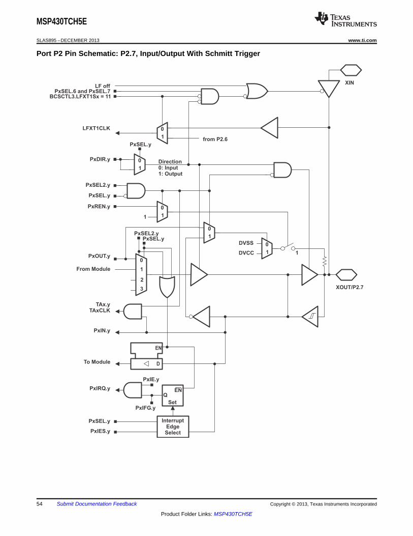
XOUT/P2.7
Direction0: Input1: Output
To Module
From Module
PxOUT.y
DVSS
DVCC 1
TAx.yTAxCLK
1
0
PxIN.y
EN
D
PxSEL.y
PxREN.y
1
0
PxDIR.y
1
0
PxSEL2.y
PxSEL.y
1
0
PxSEL.y
1
3
2
1
0
PxSEL2.y
PxIRQ.y
PxIE.y
EN
Set
Q
InterruptEdgeSelect
PxSEL.y
PxIES.y
PxIFG.y
1
0
XINLF off
LFXT1CLK
PxSEL.6 and PxSEL.7BCSCTL3.LFXT1Sx = 11
from P2.6
MSP430TCH5E
SLAS895 –DECEMBER 2013 www.ti.com
Port P2 Pin Schematic: P2.7, Input/Output With Schmitt Trigger
54 Submit Documentation Feedback Copyright © 2013, Texas Instruments Incorporated
Product Folder Links: MSP430TCH5E

MSP430TCH5E
www.ti.com SLAS895 –DECEMBER 2013
Table 22. Port P2 (P2.7) Pin FunctionsCONTROL BITS / SIGNALS (1)
PIN NAME x FUNCTION P2SEL.6 P2SEL2.6(P2.x) P2DIR.x P2SEL.7 P2SEL2.71 0XOUT/ XOUT 1 1 00 0P2.7/ 7 P2.x (I/O) I: 0; O: 1 X 00 1Pin Osc Capacitive sensing X X X
(1) X = don't care
Copyright © 2013, Texas Instruments Incorporated Submit Documentation Feedback 55
Product Folder Links: MSP430TCH5E

P3.0/TA0.2P3.1/TA1.0P3.2/TA1.1P3.3/TA1.2P3.4/TA0.0P3.5/TA0.1P3.6/TA0.2P3.7/TA1CLK/CAOUT
Direction0: Input1: Output
To Module
From Module
PxOUT.y
DVSS
DVCC 1
TAx.yTAxCLK
1
0
PxIN.y
EN
D
PxSEL.y
PxREN.y
1
0
PxDIR.y
1
0
PxSEL2.y
PxSEL.y
1
0
PxSEL.y
1
3
2
1
0
PxSEL2.y
MSP430TCH5E
SLAS895 –DECEMBER 2013 www.ti.com
Port P3 Pin Schematic: P3.0 to P3.7, Input/Output With Schmitt Trigger
56 Submit Documentation Feedback Copyright © 2013, Texas Instruments Incorporated
Product Folder Links: MSP430TCH5E

MSP430TCH5E
www.ti.com SLAS895 –DECEMBER 2013
Table 23. Port P3 (P3.0 to P3.7) Pin FunctionsCONTROL BITS / SIGNALS (1)PIN NAME x FUNCTION(P3.x) P3DIR.x P3SEL.x P3SEL2.x
P3.0/ P3.x (I/O) I: 0; O: 1 0 0TA0.2/ Timer0_A3.CCI2A 0 1 0
0Timer0_A3.TA2 1 1 0
Pin Osc Capacitive sensing X 0 1P3.1/ P3.x (I/O) I: 0; O: 1 0 0TA1.0/ 1 Timer1_A3.TA0 1 1 0Pin Osc Capacitive sensing X 0 1P3.2/ P3.x (I/O) I: 0; O: 1 0 0TA1.1/ 2 Timer1_A3.TA1 1 1 0Pin Osc Capacitive sensing X 0 1P3.3/ P3.x (I/O) I: 0; O: 1 0 0TA1.2/ 3 Timer1_A3.TA2 1 1 0Pin Osc Capacitive sensing X 0 1P3.4/ P3.x (I/O) I: 0; O: 1 0 0TA0.0/ 4 Timer0_A3.TA0 1 1 0Pin Osc Capacitive sensing X 0 1P3.5/ P3.x (I/O) I: 0; O: 1 0 0TA0.1/ 5 Timer0_A3.TA1 1 1 0Pin Osc Capacitive sensing X 0 1P3.6/ P3.x (I/O) I: 0; O: 1 0 0TA0.2/ 6 Timer0_A3.TA2 1 1 0Pin Osc Capacitive sensing X 0 1P3.7/ P3.x (I/O) I: 0; O: 1 0 0TA1CLK/ Timer1_A3.TACLK 0 1 0
7CAOUT/ Comparator output 1 1 0Pin Osc Capacitive sensing X 0 1
(1) X = don't care
Copyright © 2013, Texas Instruments Incorporated Submit Documentation Feedback 57
Product Folder Links: MSP430TCH5E

MSP430TCH5E
SLAS895 –DECEMBER 2013 www.ti.com
REVISION HISTORY
REVISION DESCRIPTIONSLAS895 Initial release
58 Submit Documentation Feedback Copyright © 2013, Texas Instruments Incorporated
Product Folder Links: MSP430TCH5E

PACKAGE OPTION ADDENDUM
www.ti.com 13-Oct-2016
Addendum-Page 1
PACKAGING INFORMATION
Orderable Device Status(1)
Package Type PackageDrawing
Pins PackageQty
Eco Plan(2)
Lead/Ball Finish(6)
MSL Peak Temp(3)
Op Temp (°C) Device Marking(4/5)
Samples
MSP430TCH5EPW NRND TSSOP PW 28 50 Green (RoHS& no Sb/Br)
CU NIPDAU Level-1-260C-UNLIM -40 to 85 430TCH5E
MSP430TCH5EPWR NRND TSSOP PW 28 2000 Green (RoHS& no Sb/Br)
CU NIPDAU Level-1-260C-UNLIM -40 to 85 430TCH5E
MSP430TCH5ERHBR NRND VQFN RHB 32 3000 Green (RoHS& no Sb/Br)
CU NIPDAU Level-2-260C-1 YEAR -40 to 85 MSP430TCH5E
MSP430TCH5ERHBT NRND VQFN RHB 32 250 Green (RoHS& no Sb/Br)
CU NIPDAU Level-2-260C-1 YEAR -40 to 85 MSP430TCH5E
(1) The marketing status values are defined as follows:ACTIVE: Product device recommended for new designs.LIFEBUY: TI has announced that the device will be discontinued, and a lifetime-buy period is in effect.NRND: Not recommended for new designs. Device is in production to support existing customers, but TI does not recommend using this part in a new design.PREVIEW: Device has been announced but is not in production. Samples may or may not be available.OBSOLETE: TI has discontinued the production of the device.
(2) Eco Plan - The planned eco-friendly classification: Pb-Free (RoHS), Pb-Free (RoHS Exempt), or Green (RoHS & no Sb/Br) - please check http://www.ti.com/productcontent for the latest availabilityinformation and additional product content details.TBD: The Pb-Free/Green conversion plan has not been defined.Pb-Free (RoHS): TI's terms "Lead-Free" or "Pb-Free" mean semiconductor products that are compatible with the current RoHS requirements for all 6 substances, including the requirement thatlead not exceed 0.1% by weight in homogeneous materials. Where designed to be soldered at high temperatures, TI Pb-Free products are suitable for use in specified lead-free processes.Pb-Free (RoHS Exempt): This component has a RoHS exemption for either 1) lead-based flip-chip solder bumps used between the die and package, or 2) lead-based die adhesive used betweenthe die and leadframe. The component is otherwise considered Pb-Free (RoHS compatible) as defined above.Green (RoHS & no Sb/Br): TI defines "Green" to mean Pb-Free (RoHS compatible), and free of Bromine (Br) and Antimony (Sb) based flame retardants (Br or Sb do not exceed 0.1% by weightin homogeneous material)
(3) MSL, Peak Temp. - The Moisture Sensitivity Level rating according to the JEDEC industry standard classifications, and peak solder temperature.
(4) There may be additional marking, which relates to the logo, the lot trace code information, or the environmental category on the device.
(5) Multiple Device Markings will be inside parentheses. Only one Device Marking contained in parentheses and separated by a "~" will appear on a device. If a line is indented then it is a continuationof the previous line and the two combined represent the entire Device Marking for that device.
(6) Lead/Ball Finish - Orderable Devices may have multiple material finish options. Finish options are separated by a vertical ruled line. Lead/Ball Finish values may wrap to two lines if the finishvalue exceeds the maximum column width.
PACKAGE OPTION ADDENDUM
www.ti.com 13-Oct-2016
Addendum-Page 2
Important Information and Disclaimer:The information provided on this page represents TI's knowledge and belief as of the date that it is provided. TI bases its knowledge and belief on informationprovided by third parties, and makes no representation or warranty as to the accuracy of such information. Efforts are underway to better integrate information from third parties. TI has taken andcontinues to take reasonable steps to provide representative and accurate information but may not have conducted destructive testing or chemical analysis on incoming materials and chemicals.TI and TI suppliers consider certain information to be proprietary, and thus CAS numbers and other limited information may not be available for release.
In no event shall TI's liability arising out of such information exceed the total purchase price of the TI part(s) at issue in this document sold by TI to Customer on an annual basis.

TAPE AND REEL INFORMATION
*All dimensions are nominal
Device PackageType
PackageDrawing
Pins SPQ ReelDiameter
(mm)
ReelWidth
W1 (mm)
A0(mm)
B0(mm)
K0(mm)
P1(mm)
W(mm)
Pin1Quadrant
MSP430TCH5EPWR TSSOP PW 28 2000 330.0 16.4 6.9 10.2 1.8 12.0 16.0 Q1
MSP430TCH5ERHBR VQFN RHB 32 3000 330.0 12.4 5.3 5.3 1.1 8.0 12.0 Q2
MSP430TCH5ERHBT VQFN RHB 32 250 180.0 12.4 5.3 5.3 1.1 8.0 12.0 Q2
PACKAGE MATERIALS INFORMATION
www.ti.com 14-Oct-2016
Pack Materials-Page 1

*All dimensions are nominal
Device Package Type Package Drawing Pins SPQ Length (mm) Width (mm) Height (mm)
MSP430TCH5EPWR TSSOP PW 28 2000 367.0 367.0 38.0
MSP430TCH5ERHBR VQFN RHB 32 3000 367.0 367.0 35.0
MSP430TCH5ERHBT VQFN RHB 32 250 210.0 185.0 35.0
PACKAGE MATERIALS INFORMATION
www.ti.com 14-Oct-2016
Pack Materials-Page 2
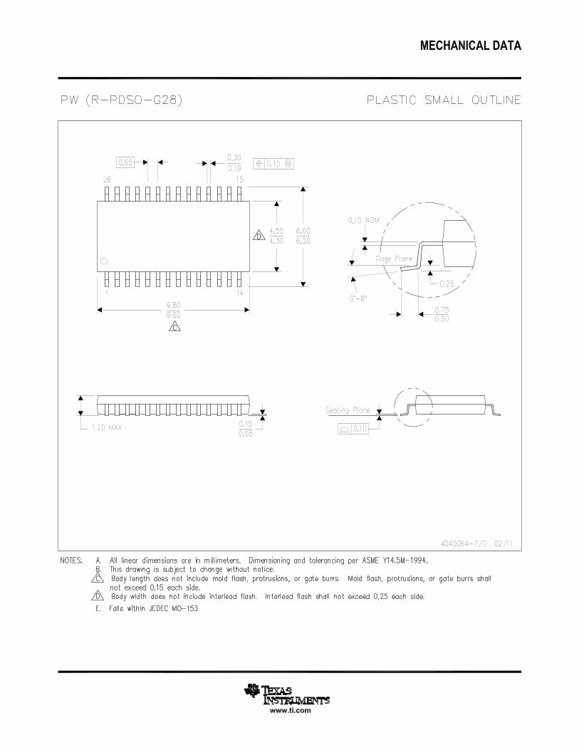


IMPORTANT NOTICE
Texas Instruments Incorporated and its subsidiaries (TI) reserve the right to make corrections, enhancements, improvements and otherchanges to its semiconductor products and services per JESD46, latest issue, and to discontinue any product or service per JESD48, latestissue. Buyers should obtain the latest relevant information before placing orders and should verify that such information is current andcomplete. All semiconductor products (also referred to herein as “components”) are sold subject to TI’s terms and conditions of salesupplied at the time of order acknowledgment.TI warrants performance of its components to the specifications applicable at the time of sale, in accordance with the warranty in TI’s termsand conditions of sale of semiconductor products. Testing and other quality control techniques are used to the extent TI deems necessaryto support this warranty. Except where mandated by applicable law, testing of all parameters of each component is not necessarilyperformed.TI assumes no liability for applications assistance or the design of Buyers’ products. Buyers are responsible for their products andapplications using TI components. To minimize the risks associated with Buyers’ products and applications, Buyers should provideadequate design and operating safeguards.TI does not warrant or represent that any license, either express or implied, is granted under any patent right, copyright, mask work right, orother intellectual property right relating to any combination, machine, or process in which TI components or services are used. Informationpublished by TI regarding third-party products or services does not constitute a license to use such products or services or a warranty orendorsement thereof. Use of such information may require a license from a third party under the patents or other intellectual property of thethird party, or a license from TI under the patents or other intellectual property of TI.Reproduction of significant portions of TI information in TI data books or data sheets is permissible only if reproduction is without alterationand is accompanied by all associated warranties, conditions, limitations, and notices. TI is not responsible or liable for such altereddocumentation. Information of third parties may be subject to additional restrictions.Resale of TI components or services with statements different from or beyond the parameters stated by TI for that component or servicevoids all express and any implied warranties for the associated TI component or service and is an unfair and deceptive business practice.TI is not responsible or liable for any such statements.Buyer acknowledges and agrees that it is solely responsible for compliance with all legal, regulatory and safety-related requirementsconcerning its products, and any use of TI components in its applications, notwithstanding any applications-related information or supportthat may be provided by TI. Buyer represents and agrees that it has all the necessary expertise to create and implement safeguards whichanticipate dangerous consequences of failures, monitor failures and their consequences, lessen the likelihood of failures that might causeharm and take appropriate remedial actions. Buyer will fully indemnify TI and its representatives against any damages arising out of the useof any TI components in safety-critical applications.In some cases, TI components may be promoted specifically to facilitate safety-related applications. With such components, TI’s goal is tohelp enable customers to design and create their own end-product solutions that meet applicable functional safety standards andrequirements. Nonetheless, such components are subject to these terms.No TI components are authorized for use in FDA Class III (or similar life-critical medical equipment) unless authorized officers of the partieshave executed a special agreement specifically governing such use.Only those TI components which TI has specifically designated as military grade or “enhanced plastic” are designed and intended for use inmilitary/aerospace applications or environments. Buyer acknowledges and agrees that any military or aerospace use of TI componentswhich have not been so designated is solely at the Buyer's risk, and that Buyer is solely responsible for compliance with all legal andregulatory requirements in connection with such use.TI has specifically designated certain components as meeting ISO/TS16949 requirements, mainly for automotive use. In any case of use ofnon-designated products, TI will not be responsible for any failure to meet ISO/TS16949.
Products ApplicationsAudio www.ti.com/audio Automotive and Transportation www.ti.com/automotiveAmplifiers amplifier.ti.com Communications and Telecom www.ti.com/communicationsData Converters dataconverter.ti.com Computers and Peripherals www.ti.com/computersDLP® Products www.dlp.com Consumer Electronics www.ti.com/consumer-appsDSP dsp.ti.com Energy and Lighting www.ti.com/energyClocks and Timers www.ti.com/clocks Industrial www.ti.com/industrialInterface interface.ti.com Medical www.ti.com/medicalLogic logic.ti.com Security www.ti.com/securityPower Mgmt power.ti.com Space, Avionics and Defense www.ti.com/space-avionics-defenseMicrocontrollers microcontroller.ti.com Video and Imaging www.ti.com/videoRFID www.ti-rfid.comOMAP Applications Processors www.ti.com/omap TI E2E Community e2e.ti.comWireless Connectivity www.ti.com/wirelessconnectivity
Mailing Address: Texas Instruments, Post Office Box 655303, Dallas, Texas 75265Copyright © 2016, Texas Instruments Incorporated