mrf24j40 data sheet - futurlec · pdf filemrf24j40 data sheet ... † microchip products...
TRANSCRIPT

© 2006 Microchip Technology Inc. Advance Information DS39776A
MRF24J40Data Sheet
IEEE 802.15.4™ 2.4 GHzRF Transceiver
Note the following details of the code protection feature on Microchip devices:
• Microchip products meet the specification contained in their particular Microchip Data Sheet.
• Microchip believes that its family of products is one of the most secure families of its kind on the market today, when used in the intended manner and under normal conditions.
• There are dishonest and possibly illegal methods used to breach the code protection feature. All of these methods, to our knowledge, require using the Microchip products in a manner outside the operating specifications contained in Microchip’s Data Sheets. Most likely, the person doing so is engaged in theft of intellectual property.
• Microchip is willing to work with the customer who is concerned about the integrity of their code.
• Neither Microchip nor any other semiconductor manufacturer can guarantee the security of their code. Code protection does not mean that we are guaranteeing the product as “unbreakable.”
Code protection is constantly evolving. We at Microchip are committed to continuously improving the code protection features of ourproducts. Attempts to break Microchip’s code protection feature may be a violation of the Digital Millennium Copyright Act. If such actsallow unauthorized access to your software or other copyrighted work, you may have a right to sue for relief under that Act.
Information contained in this publication regarding deviceapplications and the like is provided only for your convenienceand may be superseded by updates. It is your responsibility toensure that your application meets with your specifications.MICROCHIP MAKES NO REPRESENTATIONS ORWARRANTIES OF ANY KIND WHETHER EXPRESS ORIMPLIED, WRITTEN OR ORAL, STATUTORY OROTHERWISE, RELATED TO THE INFORMATION,INCLUDING BUT NOT LIMITED TO ITS CONDITION,QUALITY, PERFORMANCE, MERCHANTABILITY ORFITNESS FOR PURPOSE. Microchip disclaims all liabilityarising from this information and its use. Use of Microchipdevices in life support and/or safety applications is entirely atthe buyer’s risk, and the buyer agrees to defend, indemnify andhold harmless Microchip from any and all damages, claims,suits, or expenses resulting from such use. No licenses areconveyed, implicitly or otherwise, under any Microchipintellectual property rights.
DS39776A-page ii Advance Info
Trademarks
The Microchip name and logo, the Microchip logo, Accuron, dsPIC, KEELOQ, microID, MPLAB, PIC, PICmicro, PICSTART, PRO MATE, PowerSmart, rfPIC and SmartShunt are registered trademarks of Microchip Technology Incorporated in the U.S.A. and other countries.
AmpLab, FilterLab, Migratable Memory, MXDEV, MXLAB, SEEVAL, SmartSensor and The Embedded Control Solutions Company are registered trademarks of Microchip Technology Incorporated in the U.S.A.
Analog-for-the-Digital Age, Application Maestro, CodeGuard, dsPICDEM, dsPICDEM.net, dsPICworks, ECAN, ECONOMONITOR, FanSense, FlexROM, fuzzyLAB, In-Circuit Serial Programming, ICSP, ICEPIC, Linear Active Thermistor, Mindi, MiWi, MPASM, MPLIB, MPLINK, PICkit, PICDEM, PICDEM.net, PICLAB, PICtail, PowerCal, PowerInfo, PowerMate, PowerTool, REAL ICE, rfLAB, rfPICDEM, Select Mode, Smart Serial, SmartTel, Total Endurance, UNI/O, WiperLock and ZENA are trademarks of Microchip Technology Incorporated in the U.S.A. and other countries.
SQTP is a service mark of Microchip Technology Incorporated in the U.S.A.
All other trademarks mentioned herein are property of their respective companies.
© 2006, Microchip Technology Incorporated, Printed in the U.S.A., All Rights Reserved.
Printed on recycled paper.
rmation © 2006 Microchip Technology Inc.
Microchip received ISO/TS-16949:2002 certification for its worldwide headquarters, design and wafer fabrication facilities in Chandler and Tempe, Arizona, Gresham, Oregon and Mountain View, California. The Company’s quality system processes and procedures are for its PIC®
8-bit MCUs, KEELOQ® code hopping devices, Serial EEPROMs, microperipherals, nonvolatile memory and analog products. In addition, Microchip’s quality system for the design and manufacture of development systems is ISO 9001:2000 certified.
MRF24J40IEEE 802.15.4™ 2.4 GHz RF Transceiver
Devices Included:
• MRF24J40
Features:
• Complete IEEE 802.15.4 Specification Compliant
• Supports MiWi™, ZigBee™ and Proprietary Protocols
• Simple, 4-Wire SPI Interface• Integrated 20 MHz and 32.768 kHz Oscillator
Drive• 20 MHz Reference Clock Output:
- Available to drive microcontroller oscillator• Supports Power-Saving mode• Low-Current Consumption, Typical 18 mA in
RX mode and 22 mA in TX mode• Typical 2 μA Sleep mode
• Small, 40-Pin Leadless QFN 6x6 mm2 Package
RF/Analog Features:
• ISM Band 2.405-2.48 GHz Operation
• -91 dBm Typical Sensitivity and +5 dBm Maximum Input Level
• +0 dBm Typical Output Power and 38.75 dB TX Power Control Range
• Differential RF Input/Output and Integrated TX/RX Switch
• Integrated Low Phase Noise VCO, Frequency Synthesizer and PLL Loop Filter
• Digital VCO and Filter Calibration• Integrated RSSI ADC and I/Q DACs
• Integrated LDO• High Receiver and RSSI Dynamic Range
MAC/Baseband Features:
• Hardware CSMA-CA Mechanism, Automatic ACK Response and FCS Check
• Independent Beacon, Transmit and GTS FIFO• Hardware Security Engine (AES-128) with CTR,
CCM and CBC-MAC modes• Supports all CCA modes and RSS/LQI
• Automatic Packet Retransmit Capability• Supports In-Line or Stand-Alone modes for both
Encryption and Decryption
Pin Diagram:
40-Pin QFN
23456
1
7
VDD
RFPRFNVDD
VDD
GNDGPIO0
MRF24J40
89
GPIO1GPIO5
10GPIO4
12 13 14 15 1611 17
GP
IO2
GP
IO3
RE
SE
TG
ND
WA
KE
INT
SD
O
18 19
SD
IS
CK
20
CS
2928272625
30
24
RXQPRXIPLPOSC1LPOSC2CLKOUTGNDGND
2322
NCGND
21 VDD
3233343536 3137
VD
D
VD
D
OS
C2
OS
C1
VD
D
GN
DV
DD
3839
NC
VD
D
40
LCA
P
Note: Backside center pad is GND.
© 2006 Microchip Technology Inc. Advance Information DS39776A-page 1

MRF24J40
Table of Contents1.0 Overview ...................................................................................................................................................................................... 32.0 External Connections ................................................................................................................................................................... 73.0 Memory Organization ................................................................................................................................................................... 94.0 Serial Peripheral Interface (SPI)................................................................................................................................................. 135.0 IEEE 802.15.4™-2003 ............................................................................................................................................................... 196.0 Initialization................................................................................................................................................................................. 217.0 Transmitting and Receiving Packets .......................................................................................................................................... 298.0 Interrupts .................................................................................................................................................................................... 359.0 General Purpose I/O .................................................................................................................................................................. 3910.0 Electrical Characteristics ............................................................................................................................................................ 4111.0 Packaging Information................................................................................................................................................................ 45Appendix A: Layout and Part Selection................................................................................................................................................ 47Appendix B: MRF24J40 Schematic and Bill of Materials ..................................................................................................................... 55Index .................................................................................................................................................................................................... 59The Microchip Web Site ....................................................................................................................................................................... 61Customer Change Notification Service ................................................................................................................................................ 61Customer Support ................................................................................................................................................................................ 61Reader Response ................................................................................................................................................................................ 62Product Identification System............................................................................................................................................................... 63
TO OUR VALUED CUSTOMERS
It is our intention to provide our valued customers with the best documentation possible to ensure successful use of your Microchipproducts. To this end, we will continue to improve our publications to better suit your needs. Our publications will be refined andenhanced as new volumes and updates are introduced.
If you have any questions or comments regarding this publication, please contact the Marketing Communications Department viaE-mail at [email protected] or fax the Reader Response Form in the back of this data sheet to (480) 792-4150. Wewelcome your feedback.
Most Current Data SheetTo obtain the most up-to-date version of this data sheet, please register at our Worldwide Web site at:
http://www.microchip.com
You can determine the version of a data sheet by examining its literature number found on the bottom outside corner of any page.The last character of the literature number is the version number, (e.g., DS30000A is version A of document DS30000).
ErrataAn errata sheet, describing minor operational differences from the data sheet and recommended workarounds, may exist for currentdevices. As device/documentation issues become known to us, we will publish an errata sheet. The errata will specify the revisionof silicon and revision of document to which it applies.
To determine if an errata sheet exists for a particular device, please check with one of the following:
• Microchip’s Worldwide Web site; http://www.microchip.com• Your local Microchip sales office (see last page)When contacting a sales office, please specify which device, revision of silicon and data sheet (include literature number) you areusing.
Customer Notification SystemRegister on our web site at www.microchip.com to receive the most current information on all of our products.
DS39776A-page 2 Advance Information © 2006 Microchip Technology Inc.

MRF24J40
1.0 OVERVIEW
The MRF24J40 is an IEEE 802.15.4-2003 complianttransceiver supporting MiWi™, ZigBee™ and other pro-prietary protocols. The MRF24J40 integrates wirelessRF, PHY layer baseband and MAC layer architecturesthat can be combined with a simple microprocessor toapply low data rate to a multitude of applications thatinclude home automation, consumer electronics, PCperipherals, toys, industrial automation and more. TheMRF24J40 device integrates a receiver, transmitter,VCO and PLL into a single integrated circuit. It usesadvanced radio architecture to minimize external partcount and power consumption. The MRF24J40MAC/baseband provides hardware architecture for bothIEEE 802.15.4 MAC and PHY layers. It mainly consistsof TX/RX FIFOs, a CSMA-CA controller, superframeconstructor, receive frame filter, security engine anddigital signal processing module. The MRF24J40 isfabricated by advanced 0.18 μm CMOS process and isoffered in a 40-pin QFN 6x6 mm2 package.
Features are summarized in Table 1-1 and the pinoutfor this device is listed in Table 1-2.
The MRF24J40 consists of four major functionalblocks:
1. An SPI interface that serves as a communica-tion channel between the host controller and theMRF24J40.
2. Control registers which are used to control andmonitor the MRF24J40.
3. The MAC (Medium Access Control) module thatimplements IEEE 802.3™ compliant MAC logic.
4. The PHY (Physical Layer) driver that encodesand decodes the analog data.
The device also contains other support blocks, such asthe on-chip voltage regulator, security module andsystem control logic.
TABLE 1-1: DEVICE FEATURES FOR THE MRF24J40 (40-PIN DEVICE)
Features MRF24J40
IEEE 802.15.4™ Specification Compliant Yes
Integrated Oscillator Drive 20 MHz and 32.768 kHz
Reference Clock Output 20 MHz
Power-Saving Mode Support Yes
Current Consumption Typical 18 mA in RX and 22 mA in TX
Sleep Mode 2 μA Typical
Serial Communications SPI (4-wire)
Packages 40-Pin Leadless QFN 6x6 mm2
© 2006 Microchip Technology Inc. Advance Information DS39776A-page 3

MRF24J40
FIGURE 1-1: MRF24J40 ARCHITECTURE BLOCK DIAGRAM
Physical Layer Driver
ZigBee™ Protocol
Interrupt
Security
SPIInterface
MRF24J40
User Application
or
MiWi™ Protocolor
Proprietary Protocol
TX FIFOsLong Control
RegistersShort Control
RegistersRX FIFO
Module RX MAC
Reset
RX PHYTX PHY
TX MAC
DS39776A-page 4 Advance Information © 2006 Microchip Technology Inc.

MRF24J40
1.1 Pin Descriptions
TABLE 1-2: MRF24J40 PIN DESCRIPTIONS
Pin Symbol Type Description
1 VDD Power RF power supply. Bypass with a capacitor as close to the pin as possible.
2 RFP AIO Differential RF input/output (+).
3 RFN AIO Differential RF input/output (-).
4 VDD Power RF power supply. Bypass with a capacitor as close to the pin as possible.
5 VDD Power Guard ring power supply. Bypass with a capacitor as close to the pin as possible.
6 GND Ground Guard ring ground.
7 GPIO0 DIO General purpose digital I/O, also used as external PA enable.
8 GPIO1 DIO General purpose digital I/O, also used as external TX/RX switch control.
9 GPIO5 DIO General purpose digital I/O.
10 GPIO4 DIO General purpose digital I/O.
11 GPIO2 DIO General purpose digital I/O, also used as external TX/RX switch control.
12 GPIO3 DIO General purpose digital I/O.
13 RESET DI Global hardware Reset pin active-low.
14 GND Ground Ground for digital circuit.
15 WAKE DI External wake-up trigger.
16 INT DO Interrupt pin to microcontroller.
17 SDO DIO Serial interface data output from MRF24J40.
18 SDI DIO Serial interface data input to MRF24J40.
19 SCK DI Serial interface clock.
20 CS DI Serial interface enable.
21 VDD Power Digital circuit power supply. Bypass with a capacitor as close to the pin as possible.
22 GND Ground Ground for digital circuit.
23 NC — No Connection, do not connect anything to this pin.
24 GND Ground Ground for digital circuit.
25 GND Ground Ground for digital circuit.
26 CLKOUT DIO 20/10/5/2.5 MHz clock output.
27 LPOSC2 AI 32 kHz crystal input (-).
28 LPOSC1 AI 32 kHz crystal input (+).
29 RXIP AO Analog RX I channel output (+).
30 RXQP AO Analog RX Q channel output (+).
31 VDD Power Power supply for band gap reference circuit. Bypass with a capacitor as close to the pin as possible.
32 VDD Power Power supply for analog circuit. Bypass with a capacitor as close to the pin as possible.
33 OSC2 AI 20 MHz crystal input (-).
34 OSC1 AI 20 MHz crystal input (+).
35 VDD Power PLL power supply. Bypass with a capacitor as close to the pin as possible.
36 GND Ground Ground for PLL.
37 VDD Power Charge pump power supply. Bypass with a capacitor as close to the pin as possible.
38 NC — No Connection.
39 VDD Power VCO supply. Bypass with a capacitor as close to the pin as possible.
40 LCAP — PLL loop filter external capacitor. Connected to external 180 pF capacitor.
Legend: A = Analog, D = Digital, I = Input, O = Output
© 2006 Microchip Technology Inc. Advance Information DS39776A-page 5
MRF24J40
NOTES:
DS39776A-page 6 Advance Information © 2006 Microchip Technology Inc.

MRF24J40
2.0 EXTERNAL CONNECTIONS
2.1 Oscillator
The MRF24J40 is designed to operate at 20 MHz witha crystal connected to the OSC1 and OSC2 pins. Atypical oscillator circuit is shown in Figure 2-1.
FIGURE 2-1: CRYSTAL OSCILLATOR OPERATION
2.2 Oscillator Start-up
The MRF24J40 PHY has an internal PLL that must lockbefore the device is capable of transmitting or receivingpackets. After a full Power-on Reset, the devicerequires 2 ms to lock. During this delay, all registersand buffer memory may still be read and written tothrough the SPI bus. However, software should notattempt to transmit any packets (set the TXRTS(TXNMTRIG<0>)), or access any MAC or PHYregisters during this period.
2.3 CLKOUT Pin
The clock out pin is provided to the system designer foruse as the host controller clock or as a clock source forother devices in the system. The CLKOUT has an inter-nal prescaler which can divide the output by 1, 2, 4 or 8.The CLKOUT function is enabled via the CLKCTRLregister (Register 2-1) and the prescaler is selected viathe RFCTRL7 register (Register 2-2).Note 1: A series resistor (RS) may be required for AT
strip cut crystals.
C1
C2
XTAL
OSC2
OSC1
Logic
MRF24J40RS(1)
To Internal
REGISTER 2-1: CLKCTRL: DIVIDED SLEEP CLOCK (50 kHz) SELECTION REGISTER
R/W-0 U-0 R/W-0 R/W-0 R/W-0 R/W-0 R/W-0 R/W-0
r — CLKOEN SCLKDIV<4:0>
bit 7 bit 0
Legend:
R = Readable bit W = Writable bit U = Unimplemented bit, read as ‘0’
-n = Value at POR ‘1’ = Bit is set ‘0’ = Bit is cleared x = Bit is unknown
bit 7 Reserved: Maintain as ‘0’
bit 6 Unimplemented: Read as ‘0’
bit 5 CLKOEN: 20 MHz Clock Output Enable bit
1 = Disable0 = Enable
bit 4-0 SCLKDIV4:SCLKDIV0: Divided SLPCLK Selection bitsDivided by 2n.
© 2006 Microchip Technology Inc. Advance Information DS39776A-page 7

MRF24J40
To create a clean clock signal, the CLKOUT pin is heldlow for a period when power is first applied. After thePower-on Reset ends, the Oscillator Start-up Timer(OST) will begin counting. When the OST expires, theCLKOUT pin will begin outputting its default frequencyof 2.5 MHz (main clock divided by 8).
2.4 RF Output
RFP and RFN are the differential RF input/output pins.These pins are connected to the antenna of the system,as seen in the example circuit diagram in Figure A-1. L5is an RF choke. This inductor filters out non 2.4 GHzvoltages. L3, L4, C37 and C43 act as a balun. The balunconverts a differential unbalanced input and converts itto a balanced singled-ended output and visa versa. L1,C23 and C38 form a pi-type matching circuit to matchthe impedance of the balun to the impedance of theantenna. This circuit is not required if the impedance ofthe balun matches the antenna impedance. Referto Appendix A.1 “Layout Considerations and RFMeasurements” for more details about board layoutand part selection concerning the RF output pins.
REGISTER 2-2: RFCTRL7: RF CONTROL REGISTER 7
R/W-0 R/W-0 U-0 U-0 U-0 U-0 R/W-0 R/W-0
SLPCLK<7:6> — — — — CLKDIV<1:0>
bit 7 bit 0
Legend:
R = Readable bit W = Writable bit U = Unimplemented bit, read as ‘0’
-n = Value at POR ‘1’ = Bit is set ‘0’ = Bit is cleared x = Bit is unknown
bit 7-6 SLPCLK7:SLPCLK6: Sleep Clock Selection bits00 = None01 = External crystal10 = Internal ring oscillator11 = Reserved
bit 5-2 Unimplemented: Read as ‘0’
bit 1-0 CLKDIV1:CLKDIV0: MRF24J40 Clock Output Frequency bits
00 = 2.5 MHz01 = 5 MHz10 = 10 MHz11 = 20 MHz
DS39776A-page 8 Advance Information © 2006 Microchip Technology Inc.

MRF24J40
3.0 MEMORY ORGANIZATION
All memory in the MRF24J40 is implemented as staticRAM. There are five types of memory in theMRF24J40:
• Short Address Control Registers• Long Address Control Registers
• Transmit Buffers• Receive Buffers• Security Buffer
The control registers, both long and short, are used forconfiguration, control, and status retrieval of theMRF24J40. The control registers are directly read andwritten to by the SPI interface. The transmit and receivebuffers contain transmit and receive memory used bythe controller to transmit and receive data.
The security buffer provides an engine for theMRF24J40 MAC, which is compatible with theIEEE 802.15.4 LR-WPAN (ZigBee). The security buffercontains the following features:
• Transmit encryption and receive decryption.• Seven-mode security suite.
• 64 x 8-bit security RAM for security suite storing; one receive key and three transmit keys for TX FIFOs. Beacon FIFO and GTS2 FIFO share the same key space since they will not conflict with each other. Normal FIFO and GTS1 FIFO both have their own transmit key.
• Security of APL and NWK layers can be achieved using the same engine. The upper layer security function is compliant to the ZigBee V1.0 and ZigBee 2006 specifications.
The SPI interface used to write and read these regis-ters is described in Section 4.0 “Serial PeripheralInterface (SPI)”.
Figure 3-1 shows the data memory organization for theMRF24J40.
FIGURE 3-1: MRF24J40 MEMORY SPACE
Short AddressControl Registers
TXB FIFO
Long AddressControl Registers
Security Buffer
RX FIFO
TXN FIFO
GTS1 FIFO
GTS2 FIFO
TransmitBuffers
ControlRegisters
Security
ReceiveFIFO
000h
07Fh080h
0FFh100h
17Fh180h
1FFh
27Fh
200h
280h
2BEh
300h
38Fh
Long AddressShort AddressSpace
00h
3Fh
Unimplemented2BFh
2FFh
Space
© 2006 Microchip Technology Inc. Advance Information DS39776A-page 9

MRF24J40
3.1 Control Registers
The control registers provide the main interface betweenthe host controller and the on-chip RF controller logic.Writing to these registers controls the operation of theinterface, while reading the registers allows the hostcontroller to monitor operations.
The control register memory is partitioned into the shortaddress control register section and the long addresscontrol register section.
All reserved registers may be read but their contentsmust not be changed. When reading and writing toregisters which contain reserved bits, any rules statedin the register definition should be observed.
FIGURE 3-2: MRF24J40 SHORT ADDRESS CONTROL REGISTER MAPPING
FIGURE 3-3: MRF24J40 LONG ADDRESS CONTROL REGISTER MAPPING
RXMCR00h
PANIDL01h
PANIDH02h
SADRL03h
SADRH04h
EADR005h
EADR106h
EADR207h
EADR308h
EADR409h
EADR50Ah
EADR60Bh
EADR70Ch
RXFLUSH0Dh
—0Eh
0Fh
10h
11h
12h
13h
14h
15h
16h
17h
18h
19h
1Ah
1Bh
1Ch
1Dh
1Eh
1Fh —
—
—
—
—
—
—
—
—
—
—
—
TXNMTRIG
—
—
—
—
—20h
—21h
—22h
—23h
TXSR24h
—25h
—26h
—27h
—28h
—29h
—2Ah
—2Bh
—2Ch
—2Dh
—2Eh
2Fh
30h
31h
32h
33h
34h
35h
36h
37h
38h
39h
3Ah
3Bh
3Ch
3Dh
3Eh
3Fh —
—
ISRSTS
INTMSK
GPIO
TRISGPIO
—
RFCTL
—
—
—
BBREG2
—
—
—
BBREG6
RSSITHCCA
RFCTRL0200h
—201h
RFCTRL2202h
RFCTRL3203h
—204h
—205h
RFCTRL6206h
RFCTRL7207h
RFCTRL8208h
—209h
—20Ah
—20Bh
—20Ch
—20Dh
—20Eh
20Fh
210h
211h
212h
213h
214h
215h
216h
217h
218h
219h
21Ah
21Bh
21Ch
21Dh
21Eh
21Fh —
—
CLKINTCR
—
—
—
—
—
—
—
—
—
—
—
—
—
—
CLKCTRL220h
—221h
—222h
—223h
—224h
—225h
—226h
—227h
—228h
—229h
22Ah
—22Bh
—22Ch
—22Dh
—22Eh
22Fh
230h
231h
232h
233h
234h
235h
236h
237h
238h
239h
23Ah
23Bh
23Ch
23Dh
23Eh
23Fh —
—
—
—
—
—
—
—
—
—240h
241h
—242h
—243h
—244h
—245h
—246h
—247h
—248h
—249h
—24Ah
—24Bh
—24Ch
——
—
—
—
—
—
—
—
—
DS39776A-page 10 Advance Information © 2006 Microchip Technology Inc.

MRF24J40
3.2 MRF24J40 Address Summary
TABLE 3-1: REGISTER FILE SHORT ADDRESS SUMMARY
File Name Bit 7 Bit 6 Bit 5 Bit 4 Bit 3 Bit 2 Bit 1 Bit 0Value on
PORDetails
on page:
RXMCR TXCRCEN BBLPBK ACKEN MACLPBK PANCOORD COORD RXCRCEN PROMI 0000 0000 21
PANIDL MAC PAN Low Byte (PANL<7:0>) 0000 0000 26
PANIDH MAC PAN High Byte (PANH<15:8>) 0000 0000 26
SADRL MAC Short Address Low Byte (SADDRL<7:0>) 0000 0000 27
SADRH MAC Short Address High Byte (SADDRH<15:8>) 0000 0000 27
EADR0 LSB of EUI (EADR0<7:0>) 0000 0000 26
EADR1 Byte 2 of EUI (EADR1<15:8>) 0000 0000 26
EADR2 Byte 3 of EUI (EADR2<23:16>) 0000 0000 26
EADR3 Byte 4 of EUI (EADR3<31:24>) 0000 0000 26
EADR4 Byte 5 of EUI (EADR4<39:32>) 0000 0000 26
EADR5 Byte 6 of EUI (EADR5<47:40>) 0000 0000 26
EADR6 Byte 7 of EUI (EADR6<55:48>) 0000 0000 26
EADR7 MSB of EUI (EADR7<63:56>) 0000 0000 26
RXFLUSH — r r RXWRTBLK CMDONLY DATAONLY BCNONLY RXFLUSH -000 0000 34
TXNMTRIG — — — PENDACK INDIRECT ACKREQ SECEN TXRTS ---0 0000 30
TXSR TXRETRY<7:6> CCAFAIL r r r r r 0000 0000 31
ISRSTS SLPIF WAKEIF HSYMTMRIF SECIF RXIF GTS2TXIF GTS1TXIF TXIF 0000 0000 36
INTMSK SLPMSK WAKEMSK HSYMTMRMSK SECMSK RXMSK GTS2TXMSK GTS1TXMSK TXMSK 1111 1111 37
GPIO — — GPIO5 GPIO4 GPIO3 GPIO2 GPIO1 GPIO0 --00 0000 39
TRISGPIO — — TRISGP5 TRISGP4 TRISGP3 TRISGP2 TRISGP1 TRISGP0 --00 0000 40
RFCTL r — — r r RFRST r r 0--0 0000 24
BBREG2 CCAMODE<7:6> CCATHRES<5:2> — — 0000 00-- 25
BBREG6 RSSIREQ RXRSSI r r r r r RSSIRDY 0000 0001 25
RSSITHCCA RSSITHRES<7:0> 0000 0000 23
Legend: - = unimplemented, r = reserved. Shaded cells are unimplemented, read as ‘0’.
TABLE 3-2: REGISTER FILE LONG ADDRESS SUMMARY
File Name Bit 7 Bit 6 Bit 5 Bit 4 Bit 3 Bit 2 Bit 1 Bit 0Value on
PORDetails
on page:
RFCTRL0 CHANNEL<7:4> — — — — 0000 ---- 24
RFCTRL2 RFPLL r r r r — — — 0000 0--- 22
RFCTRL3 TXPOWER<7:3> — — — 0000 0--- 22
RFCTRL6 TXFIL — r r BATMONEN — — — 0-00 0--- 23
RFCTRL7 SLPCLK<7:6> — — — — CLKDIV<1:0> 00-- --00 8
RFCTRL8 — — — RF_VCO — — — SLPCLKOUT ---0 ---0 23
CLKINTCR — — — — — — INTEDGE SLPCLKEN ---- --00 38
CLKCTRL r — CLKOEN SCLKDIV<4:0> 0-00 0000 7
Legend: - = unimplemented, r = reserved. Shaded cells are unimplemented, read as ‘0’.
© 2006 Microchip Technology Inc. Advance Information DS39776A-page 11

MRF24J40
NOTES:
DS39776A-page 12 Advance Information © 2006 Microchip Technology Inc.

MRF24J40
4.0 SERIAL PERIPHERAL INTERFACE (SPI)
4.1 Overview
The MRF24J40 is designed to interface directly withthe Serial Peripheral Interface (SPI) port available onmany microcontrollers. The implementation used onthis device supports SPI mode 0,0 only. In addition, theSPI port requires that SCK be Idle in a low state;selectable clock polarity is not supported.
Commands and data are sent to the device via the SDIpin, with data being clocked in on the rising edge ofSCK. Data is driven out by the MRF24J40 on the SDOline, on the falling edge of SCK. The CS pin must beheld low while any operation is performed and returnedhigh when finished.
The MRF24J40 accesses the short and long RAMbanks in a slightly different manner. The followingsections describe the required waveforms in order toread and write from both short and long RAMaddresses.
FIGURE 4-1: SPI INPUT TIMING
FIGURE 4-2: SPI OUTPUT TIMING
CS
SCK
SDI
SDO
LSb InMSb In
High-Impedance State
CS
SCK
SDO MSb Out LSb Out
Don’t CareSDI
© 2006 Microchip Technology Inc. Advance Information DS39776A-page 13

MRF24J40
4.2 Short Address Register Interface
4.2.1 READING SHORT ADDRESS REGISTERS
The short address space is accessed by sending a ‘0’as the first bit of the SPI transfer. The following 6 bitsare the address of the target register. The final bit of thefirst byte is a ‘0‘ to indicate that the command is a read.On the next clock edge of SCK, the Most Significant bitof the register will shift out, followed by the rest of thebits.
FIGURE 4-3: SHORT ADDRESS READ
EXAMPLE 4-1: SHORT ADDRESS READ EXAMPLE
SCK
SDI
SDO
CS
A5 A4 A3 A2 A1 A0
D7 D6 D5 D4 D3 D2 D1 D0
X0 0
BYTE GetShortRAMAddress(BYTE address){
BYTE toReturn;CSn = 0;SPIPut((address<<1)&0b01111110);toReturn = SPIGet();CSn = 1;return toReturn;
}
DS39776A-page 14 Advance Information © 2006 Microchip Technology Inc.

MRF24J40
4.2.2 WRITING SHORT ADDRESS REGISTERS
The short address space is accessed by sending a ‘0’as the first bit of the SPI transfer. The following 6 bitsare the address of the target register. The final bit of thefirst byte is a ‘1’ to indicate that the command is a write.On the next clock edge of SCK, the Most Significant bitof the register will shift out, followed by the rest of thebits.
FIGURE 4-4: SHORT ADDRESS WRITE
EXAMPLE 4-2: SHORT ADDRESS WRITE EXAMPLE
SCK
SDI
SDO
CS
A5 A4 A3 A2 A1 A0
X
0 1 D7 D6 D5 D4 D3 D2 D1 D0
void SetShortRAMAddress(BYTE address, BYTE value){
CSn = 0;SPIPut(((address<<1)&0b01111111)|0x01);SPIPut(value);CSn = 1;
}
© 2006 Microchip Technology Inc. Advance Information DS39776A-page 15

MRF24J40
4.3 Long Address Register Interface
4.3.1 READING LONG ADDRESS REGISTERS
The long address space is accessed by sending a ‘1’as the first bit of the SPI transfer. The following 10 bitsare the address of the target register. The final bit is a‘0‘ to indicate that the command is a read. On the nextclock edge of SCK, the Most Significant bit of theregister will shift out, followed by the rest of the bits.
FIGURE 4-5: LONG ADDRESS READ
EXAMPLE 4-3: LONG ADDRESS READ EXAMPLE
SCK
SDI
SDO
CS
A9 A8 A7 A6 A5
D7 D6 D5 D4 D3 D2 D1 D0
XA4 A3 A2 A1 A0 0
X
1
BYTE GetLongRAMAddress(WORD address){
BYTE toReturn;CSn = 0;SPIPut(((address>>3)&0b01111111)|0x80);SPIPut(((address<<5)&0b11100000));toReturn = SPIGet();CSn = 1;return toReturn;
}
DS39776A-page 16 Advance Information © 2006 Microchip Technology Inc.

MRF24J40
4.3.2 WRITING LONG ADDRESS REGISTERS
The long address space is accessed by sending a ‘1 ‘as the first bit of the SPI transfer. The following 10 bitsare the address of the target register. The final bit is a‘1 ‘ to indicate that the command is a write. On the nextclock edge of SCK, the Most Significant bit of theregister will shift out, followed by the rest of the bits.
4.4 Buffer Interface
The receive and transmit buffers in the MRF24J40 arelocated in the long RAM address space. These buffersare accessed using the same process as accessing thelong RAM control addresses. The received buffer isread-only and should not be written to. The use of thesebuffers is described in Section 7.0 “Transmitting andReceiving Packets”.
FIGURE 4-6: LONG ADDRESS WRITE
EXAMPLE 4-4: LONG ADDRESS WRITE EXAMPLE
SCK
SDI
SDO
CS
A9 A8 A7 A6 A5 D7 D6 D5 D4 D3 D2 D1 D0XA4 A3 A2 A1 A0 1
X
1
void SetLongRAMAddress(WORD address, BYTE value){
CSn = 0;SPIPut((((BYTE)(address>>3))&0b01111111)|0x80);SPIPut((((BYTE)(address<<5))&0b11100000)|0x10);SPIPut(value);CSn = 1;
}
© 2006 Microchip Technology Inc. Advance Information DS39776A-page 17

MRF24J40
NOTES:
DS39776A-page 18 Advance Information © 2006 Microchip Technology Inc.

MRF24J40
5.0 IEEE 802.15.4™-2003
5.1 Overview
Before discussing the use of the MRF24J40, it may behelpful to review the structure of a typical data frame.Users requiring more information should refer to theIEEE 802.15.4 Standard.
5.2 Packet Format
Normal IEEE 802.15.4 compliant packets are between 5and 127 bytes long. They are made up of several possi-ble fields: destination address information, sourceaddress information, a length field, data payload and aCyclic Redundancy Check (CRC). Additionally, a 4-bytepreamble field and Start-of-Frame Delimiter (SFD) byteare appended to the beginning of the packet. Thus, trafficseen on the air will appear as shown in Figure 5-1.
FIGURE 5-1: PACKET FORMAT
Numberof
Bytes
4 Preamble
Field Comments
SFD1
Packet Length1
Frame Control2
DestinationAddress
Information0/4/10
Source AddressInformation
0/2/4/8/10
Sequence Number1
Data Payload0-122
FCS2 Frame check sequence – CRC
Used to
FCS
Filteredout bymodule
Start-of-Framedelimiter – Filteredout by module
Short or long address of the destinationdevice plus the PAN identifier.Length selected in the frame control.
Short or long address of the sourcedevice plus the PAN identifier.Length selected in the frame control.
Used to calculatepacket length
calculate
© 2006 Microchip Technology Inc. Advance Information DS39776A-page 19

MRF24J40
5.2.1 PREAMBLE/START-OF-FRAME DELIMITER
When transmitting and receiving data with theMRF24J40, the preamble and Start-of-Frame delimiterbytes will automatically be generated or stripped fromthe packets when they are transmitted or received. Thehost controller does not need to concern itself withthem. Normally, the host controller will also not need toconcern itself with the CRC, which the MRF24J40 willalso be able to automatically generate when transmit-ting and verify when receiving. The CRC fields will,however, be written into the receive buffer whenpackets arrive, so they may be evaluated by the hostcontroller if needed.
5.2.2 LENGTH
The length field is a 1-byte field which defines the size ofthe packet excluding itself, the preamble and SFD, butincluding all other bytes of the packet, including FCS.
5.2.3 FRAME CONTROL
The frame control field describes the format of thispacket. It defines the type of packet (beacon, data,ACK, etc.) the addressing modes used, if the packet isencrypted or not, if the packet requires an ACK and ifthe packet is an intra-PAN network. This information isused by the host controller to determine how todecipher the data that follows the frame control field.
5.2.4 SEQUENCE NUMBER
The sequence number field is a 1-byte sequence numberthat distinguishes packets. The sequence number field isused in the Acknowledgement process. An ACK packetcontains no addressing information, so the uniqueness ofthe sequence number is the sole determining factor forverifying that a packet reached its destination. TheMRF24J40 has an Auto-Acknowledgement feature thatis described in Section 7.1 “Transmitting Packets”.
5.2.5 DESTINATION ADDRESS INFORMATION
The destination address fields of an IEEE 802.15.4packet can change depending on the frame controlfield of that packet. The frame control field can specifythat no destination address is present, or can specifythat the short address (2 bytes) or long address(8 bytes) is present. In all cases where an address isspecified, the destination PAN identifier will also beincluded. On incoming packets, the MRF24J40 willfilter out packets that do not match the preconfiguredaddressing information for that radio. This eliminatesany software intervention for packets that do not meetthe addressing requirements. When transmitting thehost controller is required to write the appropriatedestination address into the transmit buffer.
5.2.6 SOURCE ADDRESS INFORMATION
The source address fields of an IEEE 802.15.4 packetcan change depending on the frame control field of thatpacket. The frame control field can specify that nodestination address is present, or can specify that theshort address (2 bytes) or long address (8 bytes) ispresent. The frame control can also specify, by usingthe intra-PAN bit, that the source PAN matches thedestination PAN and is thus, not included in the packet.
Long addresses consist of two portions. The first threebytes are known as the Extended OrganizationallyUnique Identifier (EUI). EUIs are distributed by theIEEE 802.15.4. The last five bytes are address byteswhich can contain the needed requirements at thediscretion of the company that purchased the EUI.
When transmitting packets, the assigned source long orshort address, depending on the setting of the framecontrol field, must be written into the transmit buffer bythe host controller. The MRF24J40 will not automaticallyinclude the source address information.
5.2.7 DATA
The data section of the packet can vary in length from0 bytes to 122 bytes. Packets that exceed 127 bytes,including the frame control, source addressing, desti-nation addressing, data and FCS fields, will be filteredout by the MRF24J40.
5.2.8 FCS
The FCS field is a 2-byte field which contains anindustry standard, 16-bit CRC calculated with the datafrom the frame control, sequence number, destination,source, and data fields. When receiving packets, theMRF24J40 will check the CRC of each incomingpacket. If the RXCRCEN bit (RXMCR<1>) is cleared,packets with invalid CRCs will automatically be dis-carded. If RXCRCEN is set, and the packet meets allother receive filtering criteria, the packet will be writteninto the receive buffer and the host controller will beable to determine if the CRC was valid by reading thereceive status vector (see Section 7.3 “ReceivingPackets”).
When transmitting packets, the MRF24J40 will auto-matically generate a valid CRC and transmit it attachedto the end of the packet if the TXCRCEN bit(RXMCR<7>) is cleared.
DS39776A-page 20 Advance Information © 2006 Microchip Technology Inc.

MRF24J40
6.0 INITIALIZATION
6.1 Overview
Before the MRF24J40 can be used to transmit andreceive packets, certain device settings must be initial-ized. Depending on the application, some configurationoptions may need to be changed. Normally, these tasksmay be accomplished once after Reset and do notneed to be changed thereafter.
6.2 Receive Filters
To minimize the processing requirements of the hostcontroller, the MRF24J40 incorporates several differentreceive filters which can automatically reject packetswhich are not needed. These options are controlledthrough the RXMCR register.
REGISTER 6-1: RXMCR: RECEIVE FILTER CONTROL REGISTER
R/W-0 R/W-0 R/W-0 R/W-0 R/W-0 R/W-0 R/W-0 R/W-0
TXCRCEN r ACKEN r PANCOORD COORD RXCRCEN PROMI
bit 7 bit 0
Legend:
R = Readable bit W = Writable bit U = Unimplemented bit, read as ‘0’
-n = Value at POR ‘1’ = Bit is set ‘0’ = Bit is cleared x = Bit is unknown
bit 7 TXCRCEN: No CRC Data with Normal FIFO bit1 = CRC is disabled for the TX FIFO0 = CRC is enabled for the TX FIFO
bit 6 Reserved: Maintain as ‘0’
bit 5 ACKEN: No ACK Respond in Any Case bit1 = ACK response is always disabled0 = ACK response enabled. ACKs are returned when they are requested.
bit 4 Reserved: Maintain as ‘0’
bit 3 PANCOORD: PAN Coordinator bit
1 = Set as PAN coordinator 0 = Not set as PAN coordinator
bit 2 COORD: Coordinator bit 1 = Set as coordinator 0 = Not set as coordinator
bit 1 RXCRCEN: Error Report bit 1 = RX all kinds of PKT (including CRC error)0 = Only RX PKT (CRC ok)
bit 0 PROMI: RX All Kinds of PKT bit (CRC ok)
1 = RX all kinds of PKT (CRC ok)0 = Discard PKT when there is a MAC address mismatch, illegal frame type, dPAN/sPAN or
MAC short address mismatch
© 2006 Microchip Technology Inc. Advance Information DS39776A-page 21
MRF24J40
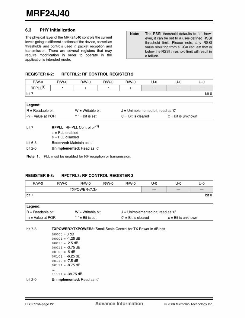
6.3 PHY Initialization
The physical layer of the MRF24J40 controls the currentlevels going to different sections of the device, as well asthresholds and controls used in packet reception andtransmission. There are several registers that mayrequire modification in order to operate in theapplication’s intended mode.
Note: The RSSI threshold defaults to ‘0’, how-ever, it can be set to a user-defined RSSIthreshold limit. Please note, any RSSIvalue resulting from a CCA request that isbelow the RSSI threshold limit will result ina failure.
REGISTER 6-2: RFCTRL2: RF CONTROL REGISTER 2
R/W-0 R/W-0 R/W-0 R/W-0 R/W-0 U-0 U-0 U-0
RFPLL(1) r r r r — — —
bit 7 bit 0
Legend:
R = Readable bit W = Writable bit U = Unimplemented bit, read as ‘0’
-n = Value at POR ‘1’ = Bit is set ‘0’ = Bit is cleared x = Bit is unknown
bit 7 RFPLL: RF-PLL Control bit(1)
1 = PLL enabled0 = PLL disabled
bit 6-3 Reserved: Maintain as ‘0’
bit 2-0 Unimplemented: Read as ‘0’
Note 1: PLL must be enabled for RF reception or transmission.
REGISTER 6-3: RFCTRL3: RF CONTROL REGISTER 3
R/W-0 R/W-0 R/W-0 R/W-0 R/W-0 U-0 U-0 U-0
TXPOWER<7:3> — — —
bit 7 bit 0
Legend:
R = Readable bit W = Writable bit U = Unimplemented bit, read as ‘0’
-n = Value at POR ‘1’ = Bit is set ‘0’ = Bit is cleared x = Bit is unknown
bit 7-3 TXPOWER7:TXPOWER3: Small Scale Control for TX Power in dB bits
00000 = 0 dB00001 = -1.25 dB00010 = -2.5 dB00011 = -3.75 dB00100 = -5 dB00101 = -6.25 dB00110 = -7.5 dB00111 = -8.75 dB… 11111 = -38.75 dB
bit 2-0 Unimplemented: Read as ‘0’
DS39776A-page 22 Advance Information © 2006 Microchip Technology Inc.

MRF24J40
REGISTER 6-4: RFCTRL6: RF CONTROL REGISTER 6
R/W-0 U-0 R/W-0 R/W-0 R/W-0 U-0 U-0 U-0
TXFIL — r r BATMONEN — — —
bit 7 bit 0
Legend:
R = Readable bit W = Writable bit U = Unimplemented bit, read as ‘0’
-n = Value at POR ‘1’ = Bit is set ‘0’ = Bit is cleared x = Bit is unknown
bit 7 TXFIL: TX Filter Control bit
Recommended value: ‘1’.
bit 6 Unimplemented: Read as ‘0’
bit 5-4 Reserved: Maintain as ‘0’
bit 3 BATMONEN: Battery Monitor Enable bit1 = Enabled0 = Disabled
bit 2-0 Unimplemented: Read as ‘0’
REGISTER 6-5: RFCTRL8: RF CONTROL REGISTER 8
U-0 U-0 U-0 R/W-0 U-0 U-0 U-0 R/W-0
— — — RF_VCO — — — SLPCLKOUT
bit 7 bit 0
Legend:
R = Readable bit W = Writable bit U = Unimplemented bit, read as ‘0’
-n = Value at POR ‘1’ = Bit is set ‘0’ = Bit is cleared x = Bit is unknown
bit 7-5 Unimplemented: Read as ‘0’
bit 4 RF_VCO: VCO Control bit1 = Enhanced VCO (recommended)0 = Normal VCO
bit 3-1 Unimplemented: Read as ‘0’
bit 0 SLPCLKOUT: 20 MHz Reference Output Clock Source bit
1 = Stabilize CLKOUT while recovering from Sleep0 = Stabilize CLKOUT after a wake from Sleep
REGISTER 6-6: RSSITHCCA: RSSI THRESHOLD FOR CCA REGISTER
R/W-0 R/W-0 R/W-0 R/W-0 R/W-0 R/W-0 R/W-0 R/W-0
RSSITHRES<7:0>
bit 7 bit 0
Legend:
R = Readable bit W = Writable bit U = Unimplemented bit, read as ‘0’
-n = Value at POR ‘1’ = Bit is set ‘0’ = Bit is cleared x = Bit is unknown
bit 7-0 RSSITHRES7:RSSITHRES0: RSSI Threshold for CCA/ED Mode bits
© 2006 Microchip Technology Inc. Advance Information DS39776A-page 23

MRF24J40
6.4 MAC Initialization
The medium access control layer of the MRF24J40consists of several registers that define how this deviceoperates on an IEEE 802.15.4 network.
6.4.1 DEVICE CONFIGURATION
The RXMCR, described in Section 6.2 “ReceiveFilters”, should be set to the appropriate value for theintended device operation. If the device is operating asa PAN coordinator, the PANCOORD bit should be set.If the device is operating as a coordinator, then theCOORD bit should be set.
6.4.2 CHANNEL SELECTION
The operational channel is selected using theRFCTRL0 register.
REGISTER 6-7: RFCTRL0: RF CONTROL REGISTER 0
R/W-0 R/W-0 R/W-0 R/W-0 U-0 U-0 U-0 U-0
CHANNEL<7:4> — — — —
bit 7 bit 0
Legend:
R = Readable bit W = Writable bit U = Unimplemented bit, read as ‘0’
-n = Value at POR ‘1’ = Bit is set ‘0’ = Bit is cleared x = Bit is unknown
bit 7-4 CHANNEL7:CHANNEL4: Channel Number bits
00000 = Channel 1100001 = Channel 1200010 = Channel 13 …11111 = Channel 26
bit 3-0 Unimplemented: Read as ‘0’
REGISTER 6-8: RFCTL: RF MODE CONTROL REGISTER
W-0 U-0 U-0 R/W-0 R/W-0 R/W-0 R/W-0 R/W-0
r — — r r RFRST r r
bit 7 bit 0
Legend:
R = Readable bit W = Writable bit U = Unimplemented bit, read as ‘0’
-n = Value at POR ‘1’ = Bit is set ‘0’ = Bit is cleared x = Bit is unknown
bit 7 Reserved: Maintain as ‘0’
bit 6-5 Unimplemented: Read as ‘0’
bit 4-3 Reserved: Maintain as ‘0’
bit 2 RFRST: RF Reset bit1 = Reset RF (turn off RF)0 = Normal operation
bit 1-0 Reserved: Maintain as ‘0’
DS39776A-page 24 Advance Information © 2006 Microchip Technology Inc.

MRF24J40
REGISTER 6-9: BBREG2: BASEBAND CCA/RSSI MODE REGISTER 2
R/W-0 R/W-0 R/W-0 R/W-0 R/W-0 R/W-0 U-0 U-0
CCAMODE<7:6> CCATHRES<5:2> — —
bit 7 bit 0
Legend:
R = Readable bit W = Writable bit U = Unimplemented bit, read as ‘0’
-n = Value at POR ‘1’ = Bit is set ‘0’ = Bit is cleared x = Bit is unknown
bit 7-6 CCAMODE7:CCAMODE6: CCA Mode bits
00 = Reserved01 = CCA Mode 1, carrier sense only10 = CCA Mode 2, energy above threshold11 = CCA Mode 3, carrier sense with energy above threshold
bit 5-2 CCATHRES5:CCATHRES2: CCA Carrier Sense Threshold bits
CCA/CS value set to 0xE or ‘1110’.
bit 1-0 Unimplemented: Read as ‘0’
REGISTER 6-10: BBREG6: BASEBAND RSSI MODE REGISTER 6
R/W-0 R/W-0 R/W-0 R/W-0 R/W-0 R/W-0 R/W-0 R-1
RSSIREQ RXRSSI r r r r r RSSIRDY
bit 7 bit 0
Legend:
R = Readable bit W = Writable bit U = Unimplemented bit, read as ‘0’
-n = Value at POR ‘1’ = Bit is set ‘0’ = Bit is cleared x = Bit is unknown
bit 7 RSSIREQ: RSSI Mode 1 bit
1 = Initiate an RSSI calculation (write back to ‘0’ when complete)0 = Otherwise
bit 6 RXRSSI: RSSI Mode 2 bit1 = Calculating RSSI for RX packet0 = No calculating RSSI for RX packet
bit 5-1 Reserved: Maintain as ‘0’
bit 0 RSSIRDY: RSSI Ready Signal Firmware Request bit
1 = RSSI value ready0 = Otherwise
© 2006 Microchip Technology Inc. Advance Information DS39776A-page 25

MRF24J40
6.4.3 LONG ADDRESSES
Every device in the world has a unique long address.Long addresses are described in more detail inSection 5.2.5 “Destination Address Information”and Section 5.2.6 “Source Address Information”.EADR0-EADR7 are eight short RAM address registersin the MRF24J40 that are used to define the device’slong address. These addresses should be loaded intothe device during the device configuration. TheMRF24J40 will automatically filter out any long addresspackets that do not match the contents ofEADR0-EADR7.
6.4.4 SHORT ADDRESS AND PAN ID
The device’s short address and PAN ID are programmedinto the MRF24J40 through the SADRL, SADRH,PANIDL and PANIDH registers. These registers are
located in the short RAM address space. TheMRF24J40 automatically filters out packets that arespecified as short address destinations with addressesthat do not match these registers. The exception to thisrule is packets with the broadcast short address (FFFFh)and/or the broadcast PAN ID (FFFFh). Packets thatmatch the short address and have the broadcast PAN IDwill be accepted, as well as packets with the broadcastshort address that match the PAN ID. A true broadcastpacket will have both the short address and PAN ID setto the broadcast address. The MRF24J40 will alsoreceive these packets no matter what the setting of theshort address and PAN ID registers.
Example 6-1 shows how to initialize the MRF24J40.
REGISTER 6-11: PANIDL: MAC PAN LOW BYTE REGISTER
R/W-0 R/W-0 R/W-0 R/W-0 R/W-0 R/W-0 R/W-0 R/W-0
MAC PAN Low Byte (PANL<7:0>)
bit 7 bit 0
Legend:
R = Readable bit W = Writable bit U = Unimplemented bit, read as ‘0’
-n = Value at POR ‘1’ = Bit is set ‘0’ = Bit is cleared x = Bit is unknown
bit 7-0 PANL7:PANL0: Lower Byte of PAN Address bits
REGISTER 6-12: PANIDH: MAC PAN HIGH BYTE REGISTER
R/W-0 R/W-0 R/W-0 R/W-0 R/W-0 R/W-0 R/W-0 R/W-0
MAC PAN High Byte (PANH<15:8>)
bit 7 bit 0
Legend:
R = Readable bit W = Writable bit U = Unimplemented bit, read as ‘0’
-n = Value at POR ‘1’ = Bit is set ‘0’ = Bit is cleared x = Bit is unknown
bit 7-0 PANH15:PANH8: Higher Byte of PAN Address bits
DS39776A-page 26 Advance Information © 2006 Microchip Technology Inc.

MRF24J40
REGISTER 6-13: SADRL: MAC SHORT ADDRESS LOW BYTE REGISTER
R/W-0 R/W-0 R/W-0 R/W-0 R/W-0 R/W-0 R/W-0 R/W-0
MAC Short Address Low Byte (SADDRL<7:0>)
bit 7 bit 0
Legend:
R = Readable bit W = Writable bit U = Unimplemented bit, read as ‘0’
-n = Value at POR ‘1’ = Bit is set ‘0’ = Bit is cleared x = Bit is unknown
bit 7-0 SADDRL7:SADDRL0: Lower Byte of Short Address bits
REGISTER 6-14: SADRH: MAC SHORT ADDRESS HIGH BYTE REGISTER
R/W-0 R/W-0 R/W-0 R/W-0 R/W-0 R/W-0 R/W-0 R/W-0
MAC Short Address High Byte (SADDRH<15:8>)
bit 7 bit 0
Legend:
R = Readable bit W = Writable bit U = Unimplemented bit, read as ‘0’
-n = Value at POR ‘1’ = Bit is set ‘0’ = Bit is cleared x = Bit is unknown
bit 7-0 SADDRH15:SADDRH8: Higher Byte of Short Address bits
© 2006 Microchip Technology Inc. Advance Information DS39776A-page 27

MRF24J40
EXAMPLE 6-1: INITIALIZING THE MRF24J40
void MRF24J40Init(void){ BYTE i; WORD j; /* place the device in hardware reset */ RESETn = 0; for(j=0;j<(WORD)300;j++){}
/* remove the device from hardware reset */ RESETn = 1; for(j=0;j<(WORD)300;j++){} /* reset the RF module */ SetShortRAMAddr(RFCTL,0x04); /* remove the RF module from reset */ SetShortRAMAddr(RFCTL,0x00); /* flush the RX fifo */ SetShortRAMAddr(WRITE_RXFLUSH,0x01); /* Program the short MAC Address, 0xffff */ SetShortRAMAddr(SADRL,0xFF); SetShortRAMAddr(SADRH,0xFF); SetShortRAMAddr(PANIDL,0xFF); SetShortRAMAddr(PANIDH,0xFF); /* Program Long MAC Address*/ for(i=0;i<(BYTE)8;i++) { SetShortRAMAddr(EADR0+i*2,myLongAddress[i]); } /* enable the RF-PLL */ SetLongRAMAddr(RFCTRL2,0x80);
/* set TX for max output power */ SetLongRAMAddr(RFCTRL3,0x00);
/* enabled TX filter control */ SetLongRAMAddr(RFCTRL6,0x80); SetLongRAMAddr(RFCTRL8,0b00010000);
/* Program CCA mode using RSSI */ SetShortRAMAddr(BBREG2,0x78); /* Enable the packet RSSI */ SetShortRAMAddr(BBREG6,0x40); /* Program CCA, RSSI threshold values */ SetShortRAMAddr(RSSITHCCA,0x00); SetLongRAMAddr(RFCTRL0,0x00); //channel 11
SetShortRAMAddr(RFCTL,0x04); //reset the RF module with new settings SetShortRAMAddr(RFCTL,0x00);}
DS39776A-page 28 Advance Information © 2006 Microchip Technology Inc.

MRF24J40
7.0 TRANSMITTING AND RECEIVING PACKETS
7.1 Transmitting Packets
The MAC inside the MRF24J40 will automaticallygenerate the preamble and Start-of-Frame delimiterfields when transmitting. Additionally, the MAC cangenerate any padding (if needed), and the CRC, ifconfigured to do so. The host controller must generateand write all other frame fields into the buffer memoryfor transmission. Before transmitting packets, the MACregisters, which alter the transmission characteristics,should be initialized as documented in Section 6.0“Initialization”.
7.2 TX FIFO Format
The TX MAC performs three major tasks conforming toIEEE 802.15.4:
• TX FIFO Control• Automatic CSMA-CA and Timing Alignments
• Hardware Superframe Handling
For TX FIFO control function, TX MAC controls4 FIFOs, including beacon, normal and 2 GTS FIFOs.When each FIFO is triggered, TX MAC performs aCSMA-CA algorithm, sends a packet to the TransmitBaseband (TXBB) at the right time, handles theretransmission if an ACK is required but not receivedand generates FCS bytes automatically.
The automatic CSMA-CA algorithm performs timingalignments, such as LIFS, SIFS and ACK turnaroundtime. The user can simply program parameters for theCSMA-CA algorithm. The TX MAC will performautomatically according these parameters.
For hardware superframe handling, TX MAC builds upthe timing frame of a superframe. It includes CAP, CFP,INACTIVE and each time slot. TX MAC sends beacon,normal and GTS FIFOs at the right time, automatically, ateach transmission. This largely reduces the complexity ofthe Beacon Enable mode of IEEE 802.15.4.
FIGURE 7-1: TRANSMIT PACKET LAYOUT
Address
Header Length
Memory Description
Packet Length(m + 3)
Frame Control
Sequence Number
Data[0]
Data[m – 1]
Length of the header. This field is described in moredetail in the security section of this document.
The length of the packet, not including the length or FCS.
The destination and source addressing information,as well as any application data.
Data[...]
0x000
0x001
0x002-0x003
0x004
0x005
The frame control field describing how this packet shouldbehave.
The sequence number distinguishing this packet.
FCS[1]
FCS[0]The CRC value for the packet; written by hardware.
0x005 + (m – 1)
0x006 + m
0x007 + m
© 2006 Microchip Technology Inc. Advance Information DS39776A-page 29

MRF24J40
7.2.1 TRIGGER PACKET TRANSMISSION
The MRF24J40 handles the Clear Channel Assess-ment (CCA) and Carrier Sense Multiple Access Colli-sion Avoidance (CSMA-CA) algorithms in hardware.The MRF24J40 also handles automatic retransmissionof packets that require an ACK. If the frame control field
of the packet requires an ACK, the ACKREQ bit(TXNMTRIG<2>) needs to be set before transmission.Once the TX FIFO is loaded with the data to transmitthe TXRTS bit (TXNMTRIG<0>) is used to transmit thepacket.
REGISTER 7-1: TXNMTRIG: TRIGGER AND SETTING FOR NORMAL FRAME (CAP) REGISTER
U-0 U-0 U-0 R-0 R/W-0 R/W-0 R/W-0 W-0
— — — PENDACK INDIRECT(1) ACKREQ(1) SECEN(1) TXRTS
bit 7 bit 0
Legend:
R = Readable bit W = Writable bit U = Unimplemented bit, read as ‘0’
-n = Value at POR ‘1’ = Bit is set ‘0’ = Bit is cleared x = Bit is unknown
bit 7-5 Unimplemented: Read as ‘0’
bit 4 PENDACK: Data Pending Status in ACK bit
Status of the data pending bit in ACK from previous transmission. This bit is reset by hardware on thenext transmission. 1 = Data pending bit was set0 = Data pending bit was cleared
bit 3 INDIRECT: Activate Indirect Transmission bit(1)
1 = Indirect transmission enabled0 = Indirect transmission disabled
bit 2 ACKREQ: TX Packet in TXN FIFO needs ACK Response bit(1)
1 = ACK requested0 = No ACK requested
bit 1 SECEN: Secure Current TX Packet bit(1)
1 = Secure packet0 = Send packet without securing it
bit 0 TXRTS: Trigger TX MAC to Send the Packet in TX FIFO bit
1 = Send the packet in the TX FIFO, automatically cleared by hardware
Note 1: This bit is cleared at the next triggering of TXN FIFO.
DS39776A-page 30 Advance Information © 2006 Microchip Technology Inc.

MRF24J40
7.2.2 TRANSMISSION STATUS
When a transmission completes, the TXIF flag of theISRSTS register will become set. Once the TXIF bit isset, the status of the transmission is located in theTXSR register.
7.3 Receiving Packets
The following section details the reception of anon-secured frame. When the MRF24J40 receives apacket that passes the MAC layer addressing, thresh-old and packet type filters, it will indicate the receptionof this packet to the host controller by setting the RXIFbit (ISRSTS<3>). The packet will remain in the bufferuntil the host frees the buffer. No other packets can bereceived while the buffer is holding a packet.
7.4 RX MAC
The RX MAC block will do CRC checking, parse thereceived frame type and address recognition, thenstore the received frame into RX FIFO. In addition tothe IEEE 802.15.4 packet, there are also 2 bytes ofinformation that are appended to the end of the packetafter the FCS field: LQI and RSSI.
The behavior of RX FIFO follows a certain rule. Whena received packet is not filtered or dropped, a receivedinterrupt/status will be issued. The interrupt isread-to-clear to save host operation time. However, theRX FIFO is flushed only using the following threemethods:
• The host reads the first byte and the last byte to the packet
• The host issues RX flush
• A software is reset
For RX filter function, the Promiscuous mode issupported to receive all FCS-ok packets. An Error modeis supported to receive all packets that successfullycorrelated PHY level preamble and delimiter.
REGISTER 7-2: TXSR: TX MAC STATUS REGISTER
R-0 R-0 R-0 R-0 R-0 R-0 R-0 R-0
TXRETRY<7:6> CCAFAIL r r r r r
bit 7 bit 0
Legend:
R = Readable bit W = Writable bit U = Unimplemented bit, read as ‘0’
-n = Value at POR ‘1’ = Bit is set ‘0’ = Bit is cleared x = Bit is unknown
bit 7-6 TXRETRY7:TXRETRY6: Retry Times bitsDefines the retry times of the most recent TXN FIFO transmission.
bit 5 CCAFAIL: Clear Channel Assessment (CCA) Status of Last Transmission bit1 = CCA failed0 = CCA passed
bit 4-0 Reserved: Maintain as ‘0’
© 2006 Microchip Technology Inc. Advance Information DS39776A-page 31

MRF24J40
FIGU
RE
7-2
:R
EC
EIV
E P
RO
CE
SS
Pac
ket R
ecei
ved
RX
IF =
1
RX
MC
R.R
XC
RC
ENN
= 1
?
Acc
ept P
acke
t
CR
C v
alid
?
NO
NO
RX
MC
R.P
RO
MI
= 1?
YES
YE
S
Long
add
ress
dest
inat
ion?
NO
NO
NO
Mat
ches
EAD
R0-
EAD
R7?
YE
S
NO
Mat
ches
SAD
RH
,SA
DR
L, P
AN
IDH
,PA
NID
L or
0xF
FFF?
YES
NO
Dat
a pa
cket
?
Bea
con
pack
et?
Com
man
dpa
cket
?
RX
FLU
SH
.DAT
Aon
ly =
1?
RX
FLU
SH
.BC
Non
ly =
1?
RX
FLU
SH
.CM
Don
ly =
1?
YE
S
YE
S
YE
S
NO
NO
NO
YE
S
YE
S
NO
NO
YE
S
Rej
ect P
acke
t
Rej
ect P
acke
t
Rej
ect P
acke
t
Rej
ect P
acke
t
YE
S
Rej
ect P
acke
t
Rej
ect P
acke
t
Acc
ept P
acke
t
Acc
ept P
acke
t
Ove
r the
Air,
NO
YE
S
YES
Sho
rt ad
dres
sde
stin
atio
n?
DS39776A-page 32 Advance Information © 2006 Microchip Technology Inc.

MRF24J40
7.4.1 RECEIVE PACKET LAYOUT
When a packet passes all of the enabled filters, it isplaced in the receive FIFO in the following format.
FIGURE 7-3: RECEIVE PACKET LAYOUT.
Address Memory Description
Packet Length(m + 5)
Frame Control
Sequence Number
Data[0]
Data[m – 1]
The length of the packet, not includingthe packet length, but does include the FCS.
The destination and source addressing informationas well as any application data.
Data[...]
0x300
0x301-0x302
0x303
0x304
The frame control field describing how this packet shouldbehave.
The sequence number distinguishing this packet.
FCS[1]
FCS[0]The CRC value for the packet; written by hardware.
0x304 + (m – 1)
0x305 + m
0x306 + m
LQI0x307 + m
RSSI0x308 + m
The link quality index of the received packet.
The received signal strength indicator for the received packet.
© 2006 Microchip Technology Inc. Advance Information DS39776A-page 33

MRF24J40
7.4.2 FREEING RECEIVE BUFFER SPACE
The RX buffer is cleared when the length byte of thepacket and the last byte of the FCS are read. Once bothof these values are read from the RX buffer, the bufferwill enable itself to receive another packet. Becausethe LQI and RSSI values are appended to the end of
the packet after the FCS, it may be advisable to readthese values out of the RX buffer before reading theFCS.
Alternatively, it is possible to clear the RX buffer byflushing it. This is done through the RXFLUSH register.
7.5 Transceiver
The MRF24J40 receiver features a low IF architectureand consists of an LNA, a pair of down conversionmixers, polyphase channel filters, baseband limiteramplifiers and RSSI technology. An ADC is used tosample the RSSI value and the sampled data is storedin a register from which the data can be read out via theSPI bus. The local oscillator generation circuits (VCO,PLL and buffers) are shared with the receiver and
transmitter. The Low Noise Amplifier (LNA) features adifferential input for high performance. The RX/TXswitch is integrated and LNA input and Power Amplifier(PA) output share the same pins. A common externalmatching network and single-ended to differential con-version is required. The transmitter features a directconversion architecture and has a 0 to -38.75 dBm out-put power. The output power adjustment is in 1.25 dBstep. The TX gain is programmed by the SPI bus.
REGISTER 7-3: RXFLUSH: RECEIVE FIFO FLUSH REGISTER
U-0 R/W-0 R/W-0 R/W-0 R/W-0 R/W-0 R/W-0 W-0
— r r RXWRTBLK CMDONLY DATAONLY BCNONLY RXFLUSH
bit 7 bit 0
Legend:
R = Readable bit W = Writable bit U = Unimplemented bit, read as ‘0’
-n = Value at POR ‘1’ = Bit is set ‘0’ = Bit is cleared x = Bit is unknown
bit 7 Unimplemented: Read as ‘0’
bit 6-5 Reserved: Maintain as ‘0’
bit 4 RXWRTBLK: Software Write to RX FIFO Address bit1 = Writing to any RX FIFO address is enabled0 = Writing to any RX FIFO address is disabled
bit 3 CMDONLY: Command Packet Receive bit1 = Only command packets are received, all other packets are filtered out0 = All valid packets are received
bit 2 DATAONLY: Data Packet Receive bit
1 = Only data packets are received, all other packets are filtered out0 = All valid packets are received
bit 1 BCNONLY: Beacon Packet Receive bit1 = Only beacon packets are received, all other packets are filtered out0 = All valid packets are received
bit 0 RXFLUSH: Flush RX FIFO Address bit1 = Flush the RX FIFO. Cleared by hardware.0 = Previous flush complete
DS39776A-page 34 Advance Information © 2006 Microchip Technology Inc.

MRF24J40
8.0 INTERRUPTS
The MRF24J40 has a simple interrupt structure. Thereis one interrupt pin that signals all of the possibleevents. The ISRSTS register is a read-to-clear registerthat specifies which interrupt(s) caused the interrupt.The INTMSK register is used to block unwanted inter-rupt sources from generating interrupts. The INTEDGEbit (CLKINTCR<1>) controls the polarity of the interruptpin. Once ISRSTS is read by the host controller, theinterrupt flags are cleared. The host controller shouldmake certain to handle all returned flags each time theISRSTS register is read.
8.1 Interrupt Structure
When an enabled interrupt occurs, the interrupt pin willremain at its interrupt state, as determined by theINTEDGE bit, until all of the flags which are causing theinterrupt are cleared or masked off (the mask bits areset) by the host controller. If more than one interruptsource is enabled, the host controller must poll eachflag in the ISRSTS register to determine the source(s)of the interrupt.
FIGURE 8-1: MRF24J40 INTERRUPT LOGIC
INTMSK.SLPMSK
ISRSTS.SLPIF
INTMSK.WAKEMSK
ISRSTS.WAKEIF
INTMSK.HSYMTMRMSK
ISRSTS.HSYMTMRIF
INTMSK.SECMSK
ISRSTS.SECIF
INTMSK.RXMSK
ISRSTS.RXIF
INTMSK.GTS2TXMSK
ISRSTS.GTS2TXIF
INTMSK.GTS1TXMSK
ISRSTS.GTS1TXIF
INTMSK.TXMSK
ISRSTS.TXIF
INT
CLKINTCR.INTEDGE
© 2006 Microchip Technology Inc. Advance Information DS39776A-page 35

MRF24J40
8.1.1 INT INTERRUPT STATUS REGISTERS
The registers associated with the INT interrupts areshown in Register 8-1, Register 8-2 and Register 8-3.
REGISTER 8-1: ISRSTS: INTERRUPT STATUS REGISTER
RC-0 RC-0 RC-0 RC-0 RC-0 RC-0 RC-0 RC-0
SLPIF WAKEIF HSYMTMRIF SECIF RXIF GTS2TXIF GTS1TXIF TXIF
bit 7 bit 0
Legend: RC = Read to clear
R = Readable bit W = Writable bit U = Unimplemented bit, read as ‘0’
-n = Value at POR ‘1’ = Bit is set ‘0’ = Bit is cleared x = Bit is unknown
bit 7 SLPIF: Sleep Alert Interrupt bit
1 = Sleep alert interrupt occurred0 = Otherwise
bit 6 WAKEIF: Wake-up Alert Interrupt bit1 = Wake-up interrupt occurred0 = Otherwise
bit 5 HSYMTMRIF: Half Symbol Timer Interrupt bit1 = Half symbol timer interrupt occurred0 = Otherwise
bit 4 SECIF: Security Key Request Interrupt bit
1 = Security key request interrupt occurred0 = Otherwise
bit 3 RXIF: RX OK Interrupt bit1 = RX OK interrupt occurred0 = Otherwise
bit 2 GTS2TXIF: GTS FIFO 2 Release Interrupt bit1 = GTS2 transmission interrupt occurred0 = Otherwise
bit 1 GTS1TXIF: GTS FIFO 1 Release Interrupt bit
1 = GTS1 transmission interrupt occurred0 = Otherwise
bit 0 TXIF: TX FIFO Release Interrupt bit1 = TX FIFO transmission interrupt occurred0 = Otherwise
DS39776A-page 36 Advance Information © 2006 Microchip Technology Inc.

MRF24J40
REGISTER 8-2: INTMSK: INTERRUPT MASK REGISTER
R/W-1 R/W-1 R/W-1 R/W-1 R/W-1 R/W-1 R/W-1 R/W-1
SLPMSK WAKEMSK HSYMTMRMSK SECMSK RXMSK GTS2TXMSK GTS1TXMSK TXMSK
bit 7 bit 0
Legend:
R = Readable bit W = Writable bit U = Unimplemented bit, read as ‘0’
-n = Value at POR ‘1’ = Bit is set ‘0’ = Bit is cleared x = Bit is unknown
bit 7 SLPMSK: Sleep Alert Mask bit0 = Enable Sleep interrupt1 = Otherwise
bit 6 WAKEMSK: Wake-up Alert Mask bit
0 = Enable Wake interrupt1 = Otherwise
bit 5 HSYMTMRMSK: Half Symbol Timer Mask bit0 = Enable half symbol timer interrupt1 = Otherwise
bit 4 SECMSK: Security Interrupt Mask bit0 = Enable security interrupt1 = Otherwise
bit 3 RXMSK: RX OK Mask bit
0 = Enable receive interrupt1 = Otherwise
bit 2 GTS2TXMSK: GTS FIFO 2 IRQ Mask bit0 = Enable GTS FIFO 2 transmit interrupt1 = Otherwise
bit 1 GTS1TXMSK: GTS FIFO 1 IRQ Mask bit0 = Enable GTS FIFO 1 transmit interrupt1 = Otherwise
bit 0 TXMSK: TX Normal FIFO IRQ Mask bit
0 = Enable normal FIFO transmit interrupt1 = Otherwise
© 2006 Microchip Technology Inc. Advance Information DS39776A-page 37

MRF24J40
REGISTER 8-3: CLKINTCR: SLPCLK ON/OFF AND INTERRUPT POLARITY REGISTER
U-0 U-0 U-0 U-0 U-0 U-0 R/W-0 R/W-0
— — — — — — INTEDGE SLPCLKEN
bit 7 bit 0
Legend:
R = Readable bit W = Writable bit U = Unimplemented bit, read as ‘0’
-n = Value at POR ‘1’ = Bit is set ‘0’ = Bit is cleared x = Bit is unknown
bit 7-2 Unimplemented: Read as ‘0’
bit 1 INTEDGE: Interrupt Edge Polarity bit
1 = Rising edge0 = Falling edge
bit 0 SLPCLKEN: Sleep Clock Enable bit1 = Disabled0 = Enabled
DS39776A-page 38 Advance Information © 2006 Microchip Technology Inc.
MRF24J40
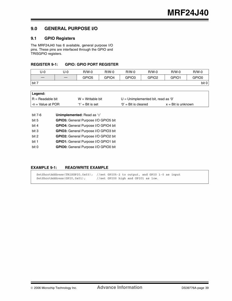
9.0 GENERAL PURPOSE I/O
9.1 GPIO Registers
The MRF24J40 has 6 available, general purpose I/Opins. These pins are interfaced through the GPIO andTRISGPIO registers.
EXAMPLE 9-1: READ/WRITE EXAMPLE
REGISTER 9-1: GPIO: GPIO PORT REGISTER
U-0 U-0 R/W-0 R/W-0 R/W-0 R/W-0 R/W-0 R/W-0
— — GPIO5 GPIO4 GPIO3 GPIO2 GPIO1 GPIO0
bit 7 bit 0
Legend:
R = Readable bit W = Writable bit U = Unimplemented bit, read as ‘0’
-n = Value at POR ‘1’ = Bit is set ‘0’ = Bit is cleared x = Bit is unknown
bit 7-6 Unimplemented: Read as ‘0’
bit 5 GPIO5: General Purpose I/O GPIO5 bit
bit 4 GPIO4: General Purpose I/O GPIO4 bit
bit 3 GPIO3: General Purpose I/O GPIO3 bit
bit 2 GPIO2: General Purpose I/O GPIO2 bit
bit 1 GPIO1: General Purpose I/O GPIO1 bit
bit 0 GPIO0: General Purpose I/O GPIO0 bit
SetShortAddress(TRISGPIO,0x03); //set GPIO5-2 to output, and GPIO 1-0 as input SetShortAddress(GPIO,0x01); //set GPIO0 high and GPIO1 as low.
© 2006 Microchip Technology Inc. Advance Information DS39776A-page 39

MRF24J40
REGISTER 9-2: TRISGPIO: GPIO PIN DIRECTION AND SPI MODE REGISTER
U-0 U-0 R/W-0 R/W-0 R/W-0 R/W-0 R/W-0 R/W-0
— — TRISGP5 TRISGP4 TRISGP3 TRISGP2 TRISGP1 TRISGP0
bit 7 bit 0
Legend:
R = Readable bit W = Writable bit U = Unimplemented bit, read as ‘0’
-n = Value at POR ‘1’ = Bit is set ‘0’ = Bit is cleared x = Bit is unknown
bit 7-6 Unimplemented: Read as ‘0’
bit 5 TRISGP5: General Purpose I/O GPIO5 Direction bit1 = Output0 = Input
bit 4 TRISGP4: General Purpose I/O GPIO4 Direction bit1 = Output0 = Input
bit 3 TRISGP3: General Purpose I/O GPIO3 Direction bit
1 = Output0 = Input
bit 2 TRISGP2: General Purpose I/O GPIO2 Direction bit1 = Output0 = Input
bit 1 TRISGP1: General Purpose I/O GPIO1 Direction bit1 = Output0 = Input
bit 0 TRISGP0: General Purpose I/O GPIO0 Direction bit
1 = Output0 = Input
DS39776A-page 40 Advance Information © 2006 Microchip Technology Inc.

MRF24J40
10.0 ELECTRICAL CHARACTERISTICS
Absolute Maximum Ratings(†)
Ambient temperature under bias.............................................................................................................. -40°C to +85°C
Storage temperature .............................................................................................................................. -65°C to +150°C
Voltage on any combined digital and analog pin with respect to VSS (except VDD)........................ -0.3V to (VDD + 0.3V)
Voltage on VDD with respect to VSS ............................................................................................................ -0.3V to 3.6V
Total power dissipation (Note 1) ...............................................................................................................................1.0W
Maximum output current sunk by GPIO1-GPIO5 pins ..............................................................................................1 mA
Maximum output current sourced by GPIO1-GPIO5 pins.........................................................................................1 mA
Maximum output current sunk by GPIO0 pin ............................................................................................................4 mA
Maximum output current sourced by GPIO0 pin .......................................................................................................4 mA
Note 1: Power dissipation is calculated as follows: Pdis = VDD x {IDD – ∑ IOH} + ∑ {(VDD – VOH) x IOH} + ∑(VOL x IOL)
† NOTICE: Stresses above those listed under “Absolute Maximum Ratings” may cause permanent damage to the device. This is a stress rating only and functional operation of the device at those or any other conditions above those indicated in the operation listings of this specification is not implied. Exposure to maximum rating conditions for extended periods may affect device reliability.
© 2006 Microchip Technology Inc. Advance Information DS39776A-page 41

MRF24J40
TABLE 10-1: RECOMMENDED OPERATING CONDITIONS
TABLE 10-2: CURRENT CONSUMPTION
Typical Values: TA = 25°C, VDD = 3.3V
TABLE 10-3: RECEIVER AC CHARACTERISTICS
Typical Values: TA = 25°C, VDD = 3.3V, LO Frequency = 2.445 GHz
Parameters Min Typ Max Units
Ambient Operating Temperature -40 — +85 °C
Supply Voltage for RF, Analog and Digital Circuits
2.4 — 3.6 V
Supply Voltage for Digital I/O 2.4 3.3 3.6 V
Input High Voltage (VIH) 0.5 x VDD — VDD + 0.3 V
Input Low Voltage (VIL) -0.3 — 0.2 x VDD V
Chip Mode Condition Min Typ Max Units
Sleep — 2 TBD μA
TX At maximum output power — 22 TBD mA
RX — 18 TBD mA
Legend: TBD = To Be Determined
Parameters Condition Min Typ Max Units
RF Input Frequency 2.4 — 2.483 GHz
RF Sensitivity At antenna input with O-QPSK signal and 3.5 dB front end loss is assumed
— -91 — dBm
Maximum RF Input LNA at high gain +5 — — dBm
LO Leakage Measured at balun matching network input at frequency 2.405-2.48 GHz
— -60 — dBm
Input Return Loss Externally matched to 50 source by a balun matching network
-12 -20 — dB
Noise Figure(including matching)
— 8 — dB
Adjacent Channel Rejection
@ +/- 5 MHz 30 — — dB
Alternate Channel Rejection
@ +/- 10 MHz 40 — — dB
RSSI Range — 50 — dB
RSSI Error -5 — 5 dB
DS39776A-page 42 Advance Information © 2006 Microchip Technology Inc.

MRF24J40
TABLE 10-4: TRANSMITTER AC CHARACTERISTICS
Typical Values: TA = 25°C, VDD = 3.3V, LO Frequency = 2.445 GHz
FIGURE 10-1: EXAMPLE SPI SLAVE MODE TIMING
TABLE 10-5: EXAMPLE SPI SLAVE MODE REQUIREMENTS
Parameters Condition Min Typ Max Units
RF Carrier Frequency 2.4 — 2.483 GHz
Maximum RF Output Power — 0 — dBm
RF Output Power Control Range — 38.75 — dB
TX Gain Control Resolution Programmed by register — 1.25 — dB
Carrier Suppression — -30 — dBc
TX Spectrum Mask for O-QPSK Signal
Offset frequency > 3.5 MHz, at 0 dBm output power
-33 — — dBm
TX EVM — — 25 %
TX Noise Floor — — -126 dBm/Hz
ParamNo.
Symbol Characteristic Min Max Units Conditions
70 TSSL2SCH CS ↓ to SCK ↑ Input 50 — ns
71 TSCH SCK Input High Time Single Byte 50 — ns
72 TSCL SCK Input Low Time Single Byte 50 — ns
74 TSCH2DIL Hold Time of SDI Data Input to SCK Edge 25 — ns
75 TDOR SDO Data Output Rise Time — 25 ns
76 TDOF SDO Data Output Fall Time — 25 ns
78 TSCR SCK Output Rise Time (Master mode) — 25 ns
80 TSCH2DOV,TSCL2DOV
SDO Data Output Valid after SCK Edge TBD — ns
82 TSSL2DOV SDO Data Output Valid after CS ↓ Edge TBD — ns
83 TSCL2SSH CS ↑ after SCK Edge 50 — ns
Legend: TBD = To Be Determined
CS
SCK
SDO
71 72
82
SDI
74
75, 76
MSb bit 6 - - - - - - 1 LSb
77
MSb In bit 6 - - - - 1 LSb In
80
8370
© 2006 Microchip Technology Inc. Advance Information DS39776A-page 43

MRF24J40
NOTES:
DS39776A-page 44 Advance Information © 2006 Microchip Technology Inc.

MRF24J40
11.0 PACKAGING INFORMATION
11.1 Package Marking Information
XXXXXXXXXX
40-Lead QFN
XXXXXXXXXXXXXXXXXXXX
YYWWNNN
MRF24J40
Example
-I/MM0610017
Legend: XX...X Product-specific informationY Year code (last digit of calendar year)YY Year code (last 2 digits of calendar year)WW Week code (week of January 1 is week ‘01’)NNN Alphanumeric traceability code Pb-free JEDEC designator for Matte Tin (Sn)* This package is Pb-free. The Pb-free JEDEC designator ( )
can be found on the outer packaging for this package.
Note: In the event the full Microchip part number cannot be marked on one line, it willbe carried over to the next line, thus limiting the number of availablecharacters for customer-specific information.
3e
3e
3e
© 2006 Microchip Technology Inc. Advance Information DS39776A-page 45

MRF24J40
11.2 Package Details
The following sections give the technical details of thepackages.
40-Lead Plastic Quad Flat, No Lead Package (MM) 6x6x0.9 mm Body [QFN] With 0.40 mm Contact Length
Note: For the most current package drawings, please see the Microchip Packaging Specification located at http://www.microchip.com/packaging
Number of Pins
Pitch
Overall Height
Standoff
Contact Thickness
Overall Width
Exposed Pad Width
Overall Length
Exposed Pad Length
Contact Width
Contact Length §
Contact-to-Exposed Pad §
Units
Dimension Limits
N
e
A
A1
A3
E
E2
D
D2
b
L
K
0.80
0.00
4.00
4.00
0.18
0.30
0.20
40
0.50 BSC
0.90
0.02
0.20 REF
6.00 BSC
4.37
6.00 BSC
4.37
0.25
0.40
—
1.00
0.05
4.75
4.75
0.30
0.50
—
MIN NOM MAX
MILLIMETERS
Notes:
1. Pin 1 visual index feature may vary, but must be located within the hatched area.
2. § Significant Characteristic
3. Package is saw singulated
4. Dimensioning and tolerancing per ASME Y14.5M
BSC: Basic Dimension. Theoretically exact value shown without tolerances.
REF: Reference Dimension, usually without tolerance, for information purposes only.
Microchip Technology Drawing No. C04–118, 09/15/06
BOTTOM VIEWTOP VIEW
D
EXPOSED PADD2
E E2
NOTE 1
A3 A1
A
12
12
N NL K
b
e
DS39776A-page 46 Advance Information © 2006 Microchip Technology Inc.

MRF24J40
APPENDIX A: LAYOUT AND PART SELECTION
A.1 Layout Considerations and RF Measurements
Below is an example of the circuit diagram of a balun.A balun is the impedance transformer from unbalancedinput of the PCB antenna and the balanced input of theRF transceiver (pins RFP and RFN).
Figure A-2 shows the measured impedance of thebalun where the center of the band is very close to 50Ω.When using low tolerance components (i.e., ±5%)along with an appropriate ground, the impedance willremain close to the 50Ω measurement. Figure A-3shows the measured impedance of the PCB antennausing a logarithmic scale magnitude. Figure A-4 showsthe same impedance using a Smith Chart diagram andFigure A-5 using a voltage standing wave ratio.
FIGURE A-1: EXAMPLE CIRCUIT DIAGRAM
FIGURE A-2: MEASURED IMPEDANCE
ANT
0.3 pF
—G
ND
L14.7 nH
0.5 pF
C380.5 pF
L35.6 nH
C430.5 pF
C40100 nF
0.5 pF
RFP
RFN
10 nH
10 nH
C7 C23
L4
C37
L5
© 2006 Microchip Technology Inc. Advance Information DS39776A-page 47

MRF24J40
FIGURE A-3: IMPEDANCE OF THE PCB ANTENNA
FIGURE A-4: IMPEDANCE OF THE PCB ANTENNA IN SMITH CHART
DS39776A-page 48 Advance Information © 2006 Microchip Technology Inc.
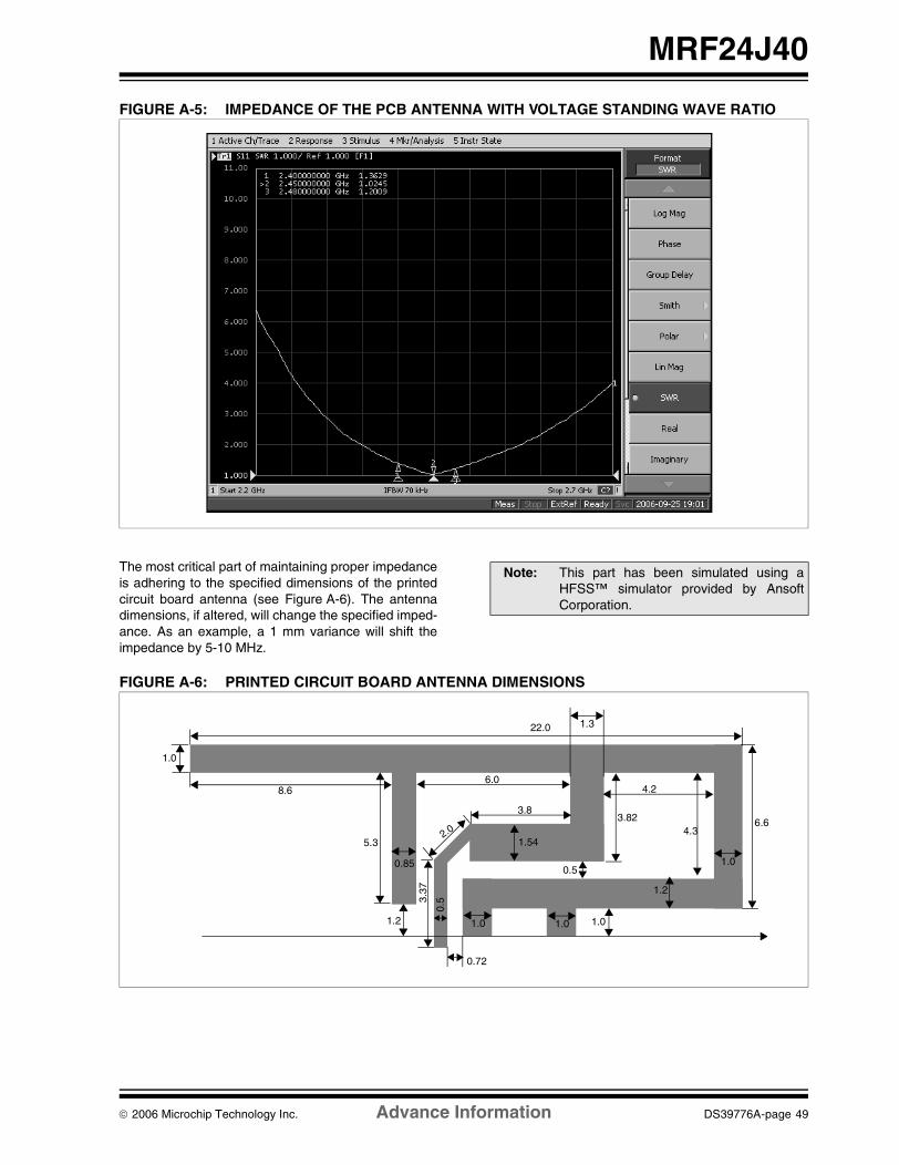
MRF24J40
FIGURE A-5: IMPEDANCE OF THE PCB ANTENNA WITH VOLTAGE STANDING WAVE RATIO
The most critical part of maintaining proper impedanceis adhering to the specified dimensions of the printedcircuit board antenna (see Figure A-6). The antennadimensions, if altered, will change the specified imped-ance. As an example, a 1 mm variance will shift theimpedance by 5-10 MHz.
FIGURE A-6: PRINTED CIRCUIT BOARD ANTENNA DIMENSIONS
Note: This part has been simulated using aHFSS™ simulator provided by AnsoftCorporation.
1.0
1.0
1.0 1.0 1.0
0.72
3.37
0.850.5
3.82
4.2
6.64.3
1.2
1.3
2.0
3.8
5.3
8.6
22.0
1.2
6.0
1.54
0.5
© 2006 Microchip Technology Inc. Advance Information DS39776A-page 49

MRF24J40
Figure A-7 and Figure A-8 illustrate simulation resultsof this PCB antenna. Note the simulation results arevery close to the measurements.
FIGURE A-7: SIMULATED PCB ANTENNA IMPEDANCE, XY PLOT
DS39776A-page 50 Advance Information © 2006 Microchip Technology Inc.

MRF24J40
FIGURE A-8: SIMULATED PCB ANTENNA IMPEDANCE, SMITH PLOT
© 2006 Microchip Technology Inc. Advance Information DS39776A-page 51

MRF24J40
A.2 PCB Layout Design
The following guidelines are intended to aid users whoare not experienced in high-frequency PCB layoutdesign.
The printed circuit board is comprised of four basic FR4layers: signal layout, RF ground, power line routing andground (see Figure A-9). The guidelines will explain therequirements of these layers.
FIGURE A-9: FOUR BASIC COPPER FR4 LAYERS
• It is important to keep the original PCB thickness since any change will affect antenna performance (see total thickness of dielectric) or microstrip lines characteristic impedance.
• The first layer width of a 50Ω characteristic impedance microstrip line is 12 mils.
• Avoid having microstrip lines longer than 2.5 cm, since that line might get very close to a quarter wave length of the working frequency of the board which is 3.0 cm, and start behaving as an antenna.
• Except for the antenna layout, avoid sharp corners since they can act as an antenna. Round corners will eliminate possible future EMI problems.
• Digital lines by definition are prone to be very noisy when handling periodic waveforms and fast clock/switching rates. Avoid laying out a RF signal close to any digital lines.
• A via filled ground patch underneath the IC transceiver is mandatory.
• A power supply must be distributed to each pin in a star topology and low-ESR capacitors must be placed at each pin for proper decoupling noise.
• Decoupling each power pin is a tedious task, especially when the noise is affecting the perfor-mance of the transceiver in a specific bandwidth. Usually, low value caps (15-27 pF) combined with large value caps (100 nF) will cover a large spectrum of frequency.
• Passive components (inductors) must be in the high-frequency category and the SRF (Self-Resonant Frequency) should be at least two times higher than the operating frequency.
Figure A-10 and Figure A-11 illustrate the ground andpower plane for the RF board.
Dielectric ε = 4.5, Thickness = 7 mils
Signal Layout, Thickness = 1.8 mils
RF Ground, Thickness = 1.2 mils
Dielectric ε = 4.5, Thickness = 19 mils
Power Line Routing, Thickness = 1.2 mils
Dielectric ε = 4.5, Thickness = 7 mils
Ground, Thickness = 1.8 mils
Note: Care should be taken with all ground lines to prevent breakage.
DS39776A-page 52 Advance Information © 2006 Microchip Technology Inc.

MRF24J40
FIGURE A-10: GROUND PLANE FIGURE A-11: POWER GROUND PLANE
M
Antenna
Note: See Figure A-6 for antenna dimensions
© 2006 Microchip Technology Inc. Advance Information DS39776A-page 53

MRF24J40
NOTES:
DS39776A-page 54 Advance Information © 2006 Microchip Technology Inc.

MRF24J40
AP
PE
ND
IX B
:M
RF
24J4
0 S
CH
EM
AT
IC A
ND
BIL
L O
F M
AT
ER
IAL
S
B.1
Sch
emat
ic
FIG
UR
E B
-1:
MR
F24
J40
SC
HE
MA
TIC
AN
T C7
0.3
pF
C38
+3.
3V
+3.
3V
+3.
3V
+3.
3V
+3.
3V
+3.
3V
+3.
3V
+3
.3V
N
L3
2.76
8 k
Hz
NL
C64
Y1
C60 N
L
C63
10 n
F
+3.
3V
C55
27 p
F
27
pF
C5
8
C54
20 p
F
20 M
Hz
Y
3C
21
20 p
F
C52
10 n
F
C53
2.2
μF
C19
27 p
F
R20
0
L5
1
0 nH
180
pF
C4
8
C40
47 p
F10
0 n
F
C39 0
.5 p
F
C37
L3 5.6
nH
0.5
pF
L4 10
nH
C44
27 p
F
C4
5
R19
10K
+3
.3V
C43
0.5
pF
MR
F24
J40
1 2 3 4 5 6 7 8 9 10
VD
D_R
F1_
3V
RF
P
RF
N
VD
D
VD
D
GN
D
GP
IO0
GP
IO1
GP
IO5
GP
IO4
GPIO2
GPIO3
RESET
GND
11
12
13
14
15
16
17
18
19
20
30 29 28 27 26 25 24 23 22 21
INT
SDO
SDI
SCK
CS
WAKE
RX
QP
RX
IP
LPO
SC
2
CLK
OU
T
GN
D
GN
D
NC
GN
D
VD
D
LPO
SC
1
40
39
38
37
36
35
34
33
32
31 VDD
VDD
OSC2
OSC1
GND
VDD
NC
VDD
LCAP
VDD
PIC
® M
icro
con
tro
ller
GP
IOS
PI
Mod
ule
RB0/INT
OS
C1
—GND
GP
IO
L1
4.7
nH
C23
0.5
pF
100
nF
Opt
iona
l
No
te:
Cen
ter
pad
on Q
FN
pac
kage
mus
t be
grou
nded
.
© 2006 Microchip Technology Inc. Advance Information DS39776A-page 55

MRF24J40
B.2 Bill of Materials
TABLE B-1: MRF24J40 DAUGHTER CARD BILL OF MATERIALS
Quantity Component NameReference
DescriptionValue Description Vendor Vendor #
1 CAP3528 C1 2.2 μF_Tant Capacitor TANT, 2.2 μF, 25V, 10%, SMD
Kemet T491B225K025AT
4 CAP0402 C23, C37, C38, C43
0.5 pF CAP, Ceramic, 0.5 pF, 50V, NP0, 0402
Yageo America 0402CG508C9B200
2 CAP0402 C21, C54 20 pF CAP, Ceramic, 20 pF, 50V, 5%, C0G, 0402
Murata Electronics
GRM1555C1H200JZ01D
4 CAP0402 C19, C44, C55, C58
27 pF CAP, Ceramic, 27 pF, 50V, 0402, SMD
Panasonic - ECG
ECJ-0EC1H270J
1 CAP0402 C40 47 pF CAP, Ceramic, 47 pF, 50V, C0G, 5%, 0402
TDK Corporation
C1005C0G1H470J
2 CAP0402 C52, C63 10 nF CAP, Ceramic, 10000 pF, 16V, X7R, 0402
Kemet C0402C103K4RACTU
2 CAP0402 C39, C45 100 nF C0402C104K8PACTU Kemet C0402C104K8PACTU
1 CAP0402 C48 180 pF CAP, Ceramic, 180 pF, 50V, C0G, 5%, 0402
TDK Corporation
C1005C0G1H181J
1 CAP0603 C53 2.2 μF CAP, Ceramic, 2.2 μF, 10V, Y5V, 0603
Taiyo Yuden LMK107F225ZA-T
1 CRYSTAL_ABM8 Y3 20 MHz Crystal, 20.000 MHz, 18 pF, FUND, SMD
Abracon Corporation
ABM8-20.000MHZ-B2-T
1 MRF24J40_QLP40 U1 MRF24J40, Single Chip Transceiver
Microchip MRF24J40-I/ML
1 IND0402 L1 4.7 nH Inductor Multilayer, 4.7 nH, 0402
TDK Corporation
MLK1005S4N7S
1 IND0402 L3 5.6 nH Inductor Multilayer, 5.6 nH, 0402
TDK Corporation
MLK1005S5N6D
2 IND0402 L4, L5 10 nH Inductor Multilayer, 10 nH, 0402
TDK Corporation
MLK1005S10NJ
2 RES0402 R20, R22 0Ω RES, 0Ω, 1/16W, 5%, 0402, SMD
Panasonic - ECG
ERJ-2GE0R00X
1 RES0402 R19 10K RES, 10 kΩ, 1/16W, 5%, 0402, SMD
Yageo America RC0402JR-0710KL
1 HDR6X2 J2 .100" Socket/Terminal Samtec LST-106-07-F-D
DS39776A-page 56 Advance Information © 2006 Microchip Technology Inc.

MRF24J40
B.3 REVISION HISTORY
Revision A (December 2006)
Original data sheet for the MRF24J40 device.
© 2006 Microchip Technology Inc. Advance Information DS39776A-page 57

MRF24J40
NOTES:
DS39776A-page 58 Advance Information © 2006 Microchip Technology Inc.

MRF24J40
INDEX
AAbsolute Maximum Ratings ................................................41AC Characteristics
Receiver .....................................................................42Transmitter .................................................................43
BBill of Materials ...................................................................56Block Diagrams
Example Circuit ..........................................................47Interrupt Logic .............................................................35MRF24J40 Architecture ................................................4Packet Format ............................................................19
Buffer Interface ...................................................................17
CCCA
Clear Channel Assessment ........................................30Channel Selection ..............................................................24Code Examples
GPIO Read/Write ........................................................39Initializing the MRF24J40 ...........................................28Long Address Read ....................................................16Long Address Write ....................................................17Short Address Read ...................................................14Short Address Write ...................................................15
Control RegistersLong Address ...............................................................9Mapping, Long Address ..............................................10Mapping, Short Address .............................................10Short Address ...............................................................9
COORD Bit .........................................................................24CSMA-CA ...........................................................................29
Carrier Sense Multiple Access Collision Avoidance ............................................30
Current Consumption .....................................................3, 42Customer Change Notification Service ...............................61Customer Notification Service ............................................61Customer Support ..............................................................61
DDevice Configuration ..........................................................24Device Overview ...................................................................3
Features (40-Pin Devices) ............................................3Differential RF Pin
NegativeRFN ......................................................................8
PositiveRFP ......................................................................8
EElectrical Characteristics ....................................................41Errata ....................................................................................2Example SPI Slave Mode Requirements ...........................43Extended Organizationally Unique Identifier (EUI) .............20External Connections ...........................................................7
CLKOUT Pin .................................................................7Oscillator .......................................................................7
Start-up .................................................................7
GGeneral Purpose I/O ..........................................................39GPIO Registers
TRISGPIOGPIO Pin Direction and
SPI Mode Register .....................................40
IIEEE 802.15.4 ......................................................................3IEEE 802.15.4-2003 ...........................................................19Impedance
Measured ...................................................................47PCB Antenna .............................................................48PCB Antenna in Smith Chart ......................................48PCB Antenna with Voltage Standing
Wave Ratio ........................................................49Simulated PCB Antenna, Smith Plot ..........................51Simulated PCB Antenna, XY Plot ..............................50
Initialization ........................................................................21Integrated Oscillator Drive ....................................................3Internet Address .................................................................61Interrupts ............................................................................35
Structure .....................................................................35
LLayout Considerations .......................................................47Long Address Register Interface ........................................16
Reading ......................................................................16Writing ........................................................................17
Long Address Summary .....................................................11Long Addresses .................................................................26
MMAC Initialization ...............................................................24Memory Organization ...........................................................9Microchip Internet Web Site ...............................................61
PPackages .............................................................................3Packaging ..........................................................................45
Details ........................................................................46Marking ......................................................................45
Packet Format ....................................................................19Cyclic Redundancy Check (CRC) ..............................19Data Field ...................................................................20Data Payload ..............................................................19Destination Address ...................................................19Destination Address Fields ........................................20FCS Field ...................................................................20Frame Control Field ...................................................20Frame Delimiter ..........................................................20Length Field ......................................................... 19, 20Sequence Number Field ............................................20Source Address ..........................................................19Source Address Fields ...............................................20
PAN ID ...............................................................................26PANCOORD Bit .................................................................24PCB
Ground plane .............................................................53Layout Design ............................................................52Power Ground Plane ..................................................53
© 2006 Microchip Technology Inc. Advance Information DS39776A-page 59

MRF24J40
PCB AntennaDimensions ................................................................ 49Simulation Results ..................................................... 50
PHY Initialization ................................................................ 22Pin Descriptions ................................................................... 5
CLKOUT (Clock Output) .............................................. 5CS (Serial Interface Enable) ........................................ 5GND (Ground, Digital Circuit) ...................................... 5GND (Ground, PLL) ..................................................... 5GND (Guard Ring Ground) .......................................... 5GPIO0 (External PA Enable) ....................................... 5GPIO1 (External TX/RX Switch Control) ...................... 5GPIO2 (External TX/RX Switch Control) ...................... 5GPIO3 (General Purpose Digital I/O) ........................... 5GPIO4 (General Purpose Digital I/O) ........................... 5GPIO5 (General Purpose Digital I/O) ........................... 5INT (Interrupt Pin) ........................................................ 5LCAP (PLL Loop Filter External Capacitor) ................. 5LPOSC1 (32 kHz Crystal Input) ................................... 5LPOSC2 (32 kHz Crystal Input) ................................... 5NC (No Connection) ..................................................... 5OSC1 (20 MHz Crystal Input) ...................................... 5OSC2 (20 MHz Crystal Input) ...................................... 5RESET (Global Hardware Reset Active-Low) .............. 5RFN (Differential RF Pin, Negative) ............................. 5RFP (Differential RF Pin, Positive) ............................... 5RXIP (Analog RX I Channel Output) ............................ 5RXQP (Analog RX Q Channel Output) ........................ 5SCK (Serial Interface Clock) ........................................ 5SDI (Serial Interface Data Input) .................................. 5SDO (Serial Interface Data Output) ............................. 5VDD (Charge Pump Power Supply) .............................. 5VDD (Digital Circuit Power Supply) ............................... 5VDD (Guard Ring Power Supply) .................................. 5VDD (PLL Power Supply) .............................................. 5VDD (Power Supply, Analog Circuit) ............................. 5VDD (Power Supply, Band Gap
Reference Circuit) ................................................ 5VDD (RF Power Supply) ............................................... 5VDD (VCO Supply) ....................................................... 5WAKE (External Wake-up Trigger) .............................. 5
Power-Saving Mode ............................................................. 3Proprietary Protocols ............................................................ 1
MiWi ............................................................................. 1ZigBee ...................................................................... 1, 9
RReader Response .............................................................. 62Receive Buffers .................................................................... 9Receive Filters ................................................................... 21Receive Packets ................................................................ 21Receive Process Flowchart ................................................ 32Receiving Packets .............................................................. 31
Freeing Buffer Space ................................................. 34Layout ........................................................................ 33
Recommended Operating Conditions ................................ 42Reference Clock Output ....................................................... 3Register File Summary ....................................................... 11Registers
BBREG2 (Baseband CCA/RSSI Mode 2) .................. 25BBREG6 (Baseband RSSI Mode 6) .......................... 25CLKCTRL (Divided Sleep Clock Selection) ................. 7CLKINTCR (SLPCLK On/Off and
Interrupt Polarity) ............................................... 38GPIO (GPIO Port) ...................................................... 39INTMSK (Interrupt Mask) ........................................... 37
ISRSTS (Interrupt Status) .......................................... 36PANIDH (MAC PAN High Byte) ................................. 26PANIDL (MAC PAN Low Byte) .................................. 26RFCTL (RF Mode Control) ........................................ 24RFCTRL0 (RF Control 0) ........................................... 24RFCTRL2 (RF Control 2) ........................................... 22RFCTRL3 (RF Control 3) ........................................... 22RFCTRL6 (RF Control 6) ........................................... 23RFCTRL7 (RF Control 7) ............................................. 8RFCTRL8 (RF Control 8) ........................................... 23RSSITHCCA (RSSI Threshold for CCA) ................... 23RXFLUSH (Receive FIFO Flush) ............................... 34RXMCR (Receive Filter Control) ................................ 21SADRH (MAC Short Address High Byte) .................. 27SADRL (MAC Short Address Low Byte) .................... 27TRISGPIO (GPIO Pin Direction
and SPI Mode) ................................................... 40TXNMTRIG (Trigger and Setting
for Normal Frame, CAP) .................................... 30TXSR (TX MAC Status) ............................................. 31
RF Measurements ............................................................. 47RF Output ............................................................................ 8RF Transceiver .................................................................. 47RSSI Default Threshold ..................................................... 22RX FIFO ............................................................................. 31RX MAC ............................................................................. 31
SSchematic .......................................................................... 55Security Buffer ..................................................................... 9Serial Communications ........................................................ 3Serial Peripheral Interface (SPI) ........................................ 13Short Address Register Interface ....................................... 14
Reading ..................................................................... 14Writing ....................................................................... 15
Short Address Summary .................................................... 11Short Addresses ................................................................ 26Sleep Mode .......................................................................... 3
TTiming Diagrams
Example SPI Slave Mode .......................................... 43Long Address Read ................................................... 16Long Address Write ................................................... 17Short Address Read .................................................. 14Short Address Write ................................................... 15SPI Input .................................................................... 13SPI Output ................................................................. 13
Transmit Buffers .................................................................. 9Transmit Packets ............................................................... 21Transmitting Packets ......................................................... 29
Status ........................................................................ 31Trigger Packet ........................................................... 30
TX FIFO ............................................................................. 30TX FIFO Format ................................................................. 29TX MAC ............................................................................. 29
WWWW Address .................................................................. 61WWW, On-Line Support ...................................................... 2
ZZigbee V1.0 Specification .................................................... 9
DS39776A-page 60 Advance Information © 2006 Microchip Technology Inc.

MRF24J40
THE MICROCHIP WEB SITE
Microchip provides online support via our WWW site atwww.microchip.com. This web site is used as a meansto make files and information easily available tocustomers. Accessible by using your favorite Internetbrowser, the web site contains the followinginformation:
• Product Support – Data sheets and errata, application notes and sample programs, design resources, user’s guides and hardware support documents, latest software releases and archived software
• General Technical Support – Frequently Asked Questions (FAQ), technical support requests, online discussion groups, Microchip consultant program member listing
• Business of Microchip – Product selector and ordering guides, latest Microchip press releases, listing of seminars and events, listings of Microchip sales offices, distributors and factory representatives
CUSTOMER CHANGE NOTIFICATION SERVICE
Microchip’s customer notification service helps keepcustomers current on Microchip products. Subscriberswill receive e-mail notification whenever there arechanges, updates, revisions or errata related to aspecified product family or development tool of interest.
To register, access the Microchip web site atwww.microchip.com, click on Customer ChangeNotification and follow the registration instructions.
CUSTOMER SUPPORT
Users of Microchip products can receive assistancethrough several channels:
• Distributor or Representative
• Local Sales Office• Field Application Engineer (FAE)• Technical Support
• Development Systems Information Line
Customers should contact their distributor,representative or field application engineer (FAE) forsupport. Local sales offices are also available to helpcustomers. A listing of sales offices and locations isincluded in the back of this document.
Technical support is available through the web siteat: http://support.microchip.com
© 2006 Microchip Technology Inc. Advance Information DS39776A-page 61

MRF24J40
READER RESPONSE
It is our intention to provide you with the best documentation possible to ensure successful use of your Microchip prod-uct. If you wish to provide your comments on organization, clarity, subject matter, and ways in which our documentationcan better serve you, please FAX your comments to the Technical Publications Manager at (480) 792-4150.
Please list the following information, and use this outline to provide us with your comments about this document.
To: Technical Publications Manager
RE: Reader Response
Total Pages Sent ________
From: Name
Company
Address
City / State / ZIP / Country
Telephone: (_______) _________ - _________
Application (optional):
Would you like a reply? Y N
Device: Literature Number:
Questions:
FAX: (______) _________ - _________
DS39776A MRF24J40
1. What are the best features of this document?
2. How does this document meet your hardware and software development needs?
3. Do you find the organization of this document easy to follow? If not, why?
4. What additions to the document do you think would enhance the structure and subject?
5. What deletions from the document could be made without affecting the overall usefulness?
6. Is there any incorrect or misleading information (what and where)?
7. How would you improve this document?
DS39776A-page 62 Advance Information © 2006 Microchip Technology Inc.

© 2006 Microchip Technology Inc. Advance Information DS39776A-page 63
MRF24J40
PRODUCT IDENTIFICATION SYSTEM
To order or obtain information, e.g., on pricing or delivery, refer to the factory or the listed sales office.
PART NO. X /XX XXX
PatternPackageTemperatureRange
Device
Device MRF24J40: IEEE 802.15.4™ 2.4 GHz RF Transceiver
Temperature Range I = -40°C to +85°C (Industrial)
Package MM = QFN (Plastic Quad Flat, No Lead)
Example:
a) MRF24J40-I/MM: Industrial temperature, QFN package.

DS39776A-page 64 Advance Information © 2006 Microchip Technology Inc.
AMERICASCorporate Office2355 West Chandler Blvd.Chandler, AZ 85224-6199Tel: 480-792-7200 Fax: 480-792-7277Technical Support: http://support.microchip.comWeb Address: www.microchip.com
AtlantaAlpharetta, GA Tel: 770-640-0034 Fax: 770-640-0307
BostonWestborough, MA Tel: 774-760-0087 Fax: 774-760-0088
ChicagoItasca, IL Tel: 630-285-0071 Fax: 630-285-0075
DallasAddison, TX Tel: 972-818-7423 Fax: 972-818-2924
DetroitFarmington Hills, MI Tel: 248-538-2250Fax: 248-538-2260
KokomoKokomo, IN Tel: 765-864-8360Fax: 765-864-8387
Los AngelesMission Viejo, CA Tel: 949-462-9523 Fax: 949-462-9608
Santa ClaraSanta Clara, CA Tel: 408-961-6444Fax: 408-961-6445
TorontoMississauga, Ontario, CanadaTel: 905-673-0699 Fax: 905-673-6509
ASIA/PACIFICAsia Pacific OfficeSuites 3707-14, 37th FloorTower 6, The GatewayHabour City, KowloonHong KongTel: 852-2401-1200Fax: 852-2401-3431
Australia - SydneyTel: 61-2-9868-6733Fax: 61-2-9868-6755
China - BeijingTel: 86-10-8528-2100 Fax: 86-10-8528-2104
China - ChengduTel: 86-28-8665-5511Fax: 86-28-8665-7889
China - FuzhouTel: 86-591-8750-3506 Fax: 86-591-8750-3521
China - Hong Kong SARTel: 852-2401-1200 Fax: 852-2401-3431
China - QingdaoTel: 86-532-8502-7355Fax: 86-532-8502-7205
China - ShanghaiTel: 86-21-5407-5533 Fax: 86-21-5407-5066
China - ShenyangTel: 86-24-2334-2829Fax: 86-24-2334-2393
China - ShenzhenTel: 86-755-8203-2660 Fax: 86-755-8203-1760
China - ShundeTel: 86-757-2839-5507 Fax: 86-757-2839-5571
China - WuhanTel: 86-27-5980-5300Fax: 86-27-5980-5118
China - XianTel: 86-29-8833-7250Fax: 86-29-8833-7256
ASIA/PACIFICIndia - BangaloreTel: 91-80-4182-8400 Fax: 91-80-4182-8422
India - New DelhiTel: 91-11-4160-8631Fax: 91-11-4160-8632
India - PuneTel: 91-20-2566-1512Fax: 91-20-2566-1513
Japan - YokohamaTel: 81-45-471- 6166 Fax: 81-45-471-6122
Korea - GumiTel: 82-54-473-4301Fax: 82-54-473-4302
Korea - SeoulTel: 82-2-554-7200Fax: 82-2-558-5932 or 82-2-558-5934
Malaysia - PenangTel: 60-4-646-8870Fax: 60-4-646-5086
Philippines - ManilaTel: 63-2-634-9065Fax: 63-2-634-9069
SingaporeTel: 65-6334-8870Fax: 65-6334-8850
Taiwan - Hsin ChuTel: 886-3-572-9526Fax: 886-3-572-6459
Taiwan - KaohsiungTel: 886-7-536-4818Fax: 886-7-536-4803
Taiwan - TaipeiTel: 886-2-2500-6610 Fax: 886-2-2508-0102
Thailand - BangkokTel: 66-2-694-1351Fax: 66-2-694-1350
EUROPEAustria - WelsTel: 43-7242-2244-39Fax: 43-7242-2244-393Denmark - CopenhagenTel: 45-4450-2828 Fax: 45-4485-2829
France - ParisTel: 33-1-69-53-63-20 Fax: 33-1-69-30-90-79
Germany - MunichTel: 49-89-627-144-0 Fax: 49-89-627-144-44
Italy - Milan Tel: 39-0331-742611 Fax: 39-0331-466781
Netherlands - DrunenTel: 31-416-690399 Fax: 31-416-690340
Spain - MadridTel: 34-91-708-08-90Fax: 34-91-708-08-91
UK - WokinghamTel: 44-118-921-5869Fax: 44-118-921-5820
WORLDWIDE SALES AND SERVICE
10/19/06