motion spm 5 series fsb50325a, fsb50325at, fsb50325as
TRANSCRIPT
© Semiconductor Components Industries, LLC, 2019
October, 2019 − Rev. 31 Publication Order Number:
FSB50325A/D
Motion SPM� 5 Series
FSB50325A, FSB50325AT,FSB50325AS
General DescriptionThe FSB50325A/AT/AS is an advanced Motion SPM 5 module
providing a fully−featured, high−performance inverter output stagefor AC Induction, BLDC and PMSM motors. These modules integrateoptimized gate drive of the built−in MOSFETs (FRFET® technology)to minimize EMI and losses, while also providing multiple on−moduleprotection features including under−voltage lockouts and thermalmonitoring. The built−in high−speed HVIC requires only a singlesupply voltage and translates the incoming logic−level gate inputs tothe high−voltage, high−current drive signals required to properly drivethe module’s internal MOSFETs. Separate open−source MOSFETterminals are available for each phase to support the widest variety ofcontrol algorithms.
Features• UL Certified No. E209204 (UL1557)
• 250 V RDS(on) = 1.7 � (Max) FRFET MOSFET 3−Phase Inverterwith Gate Drivers and Protection
• Built−in Bootstrap Diodes Simplify PCB Layout
• Separate Open−Source Pins from Low−Side MOSFETs forThree−Phase Current−Sensing
• Active−HIGH Interface, Works with 3.3 / 5 V Logic, Schmitt−triggerInput
• Optimized for Low Electromagnetic Interference
• HVIC Temperature−Sensing Built−in for Temperature Monitoring
• HVIC for Gate Driving and Under−Voltage Protection
• Isolation Rating: 1500 Vrms / 1 min.
• Moisture Sensitive Level (MSL) 3 − FSB50325AS
• These Devices are Pb−Free and are RoHS Compliant
Applications• 3−Phase Inverter Driver for Small Power AC Motor Drives
Related Source• RD−FSB50450A − Reference Design for Motion SPM 5 Series Ver.2
• AN−9082 − Motion SPM5 Series Thermal Performance by ContactPressure
• AN−9080 − User’s Guide for Motion SPM 5 Series V2
www.onsemi.com
MARKING DIAGRAM
$Y = ON Semiconductor LogoFSB50325x = Specific Device Code
(x = A, AT, AS)&Z = Assembly Plant Code&K = 2−Digits Lot Run Traceability Code&E = Designate Space&3 = 3−Digits Data Code Format
See detailed ordering and shipping information on page 2 ofthis data sheet.
ORDERING INFORMATION
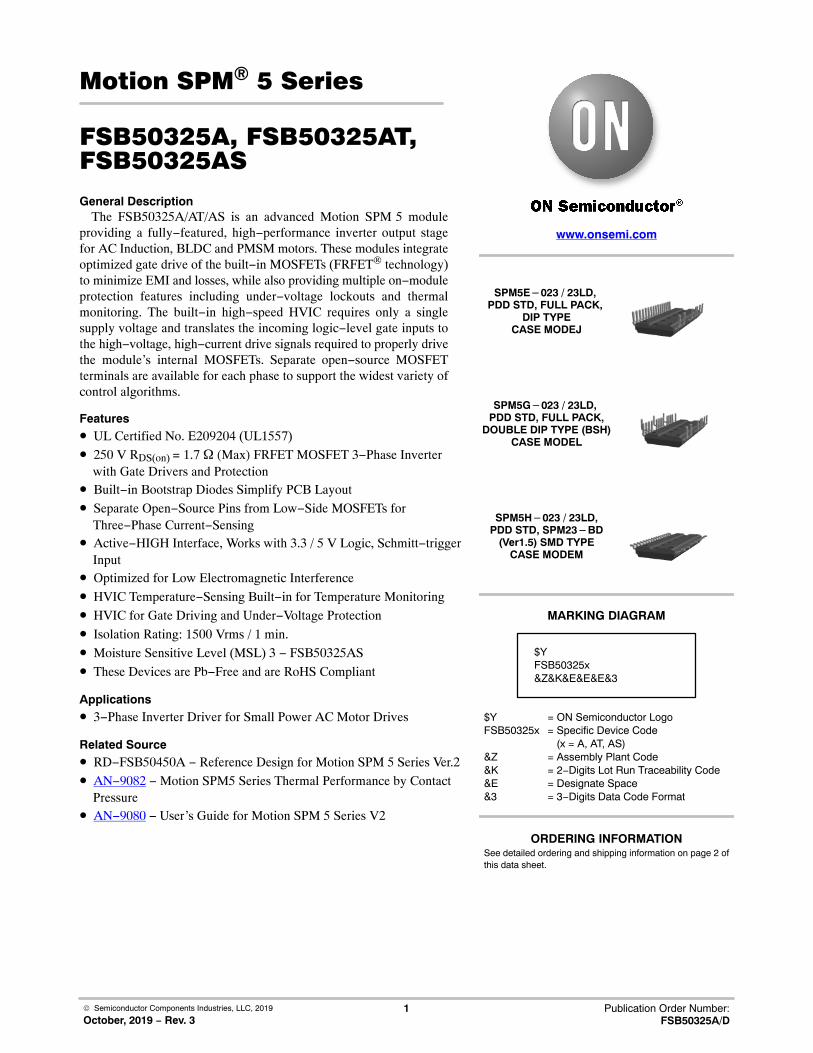
SPM5E�023 / 23LD, PDD STD, FULL PACK,
DIP TYPECASE MODEJ
SPM5G�023 / 23LD, PDD STD, FULL PACK,
DOUBLE DIP TYPE (BSH)CASE MODEL
SPM5H�023 / 23LD,PDD STD, SPM23�BD
(Ver1.5) SMD TYPECASE MODEM
$YFSB50325x&Z&K&E&E&E&3

FSB50325A, FSB50325AT, FSB50325AS
www.onsemi.com2
ORDERING INFORMATION
Device Device Marking Package Shipping†
FSB50325A FSB50325A SPM5E−023(Pb−Free)
270 / Tube
FSB50325AT FSB50325AT SPM5G−023(Pb−Free)
180 / Tube
FSB50325AS FSB50325AS SPM5H−023(Pb−Free)
450 / Tape & Reel
†For information on tape and reel specifications, including part orientation and tape sizes, please refer to our Tape and Reel PackagingSpecifications Brochure, BRD8011/D.
ABSOLUTE MAXIMUM RATINGS
Symbol Parameter Condition 1 Rating Unit
INVERTER PART (each MOSFET unless otherwise specified.)
VDSS Drain−Source Voltage of Each MOSFET 250 V
*ID 25 Each MOSFET Drain Current, Continuous TC = 25°C 1.7 A
*ID 80 Each MOSFET Drain Current, Continuous TC = 80°C 1.3 A
*IDP Each MOSFET Drain Current, Peak TC = 25°C, PW < 100 ms 4.4 A
*IDRMS Each MOSFET Drain Current, Rms TC = 80°C, FPWM < 20 kHz 0.9 Arms
*PD Maximum Power Dissipation TC = 25°C, For Each MOSFET 12.3 W
CONTROL PART (each HVIC unless otherwise specified.)
VCC Control Supply Voltage Applied Between VCC and COM 20 V
VBS High−side Bias Voltage Applied Between VB and VS 20 V
VIN Input Signal Voltage Applied Between IN and COM −0.3~VCC + 0.3 V
BOOTSTRAP DIODE PART (each bootstrap diode unless otherwise specified.)
VRRMB Maximum Repetitive Reverse Voltage 250 V
* IFB Forward Current TC = 25°C 0.5 A
* IFPB Forward Current (Peak) TC = 25°C, Under 1 ms Pulse Width 1.5 A
THERMAL RESISTANCE
R�JC Junction to Case Thermal Resistance Each MOSFET under Inverter Operating Condition (Note 1)
10.2 °C/W
TOTAL SYSTEM
TJ Operating Junction Temperature −40~150 °C
TSTG Storage Temperature −40~125 °C
VISO Isolation Voltage 60 Hz, Sinusoidal, 1 Minute, Connect Pins to Heat Sink Plate
1500 Vrms
Stresses exceeding those listed in the Maximum Ratings table may damage the device. If any of these limits are exceeded, device functionalityshould not be assumed, damage may occur and reliability may be affected.1. For the measurement point of case temperature TC, please refer to Figure 4.2. Marking “ * ” is calculation value or design factor.

FSB50325A, FSB50325AT, FSB50325AS
www.onsemi.com3
PIN DESCRIPTION
Pin No. Pin Name Description
1 COM IC Common Supply Ground
2 VB(U) Bias Voltage for U−Phase High−Side MOSFET Driving
3 VCC(U) Bias Voltage for U−Phase IC and Low−Side MOSFET Driving
4 IN(UH) Signal Input for U−Phase High−Side
5 IN(UL) Signal Input for U−Phase Low−Side
6 N.C No Connection
7 VB(V) Bias Voltage for V−Phase High Side MOSFET Driving
8 VCC(V) Bias Voltage for V−Phase IC and Low Side MOSFET Driving
9 IN(VH) Signal Input for V−Phase High−Side
10 IN(VL) Signal Input for V−Phase Low−Side
11 VTS Output for HVIC Temperature Sensing
12 VB(W) Bias Voltage for W−Phase High−Side MOSFET Driving
13 VCC(W) Bias Voltage for W−Phase IC and Low−Side MOSFET Driving
14 IN(WH) Signal Input for W−Phase High−Side
15 IN(WL) Signal Input for W−Phase Low−Side
16 N.C No Connection
17 P Positive DC−Link Input
18 U, VS(U) Output for U−Phase & Bias Voltage Ground for High−Side MOSFET Driving
19 NU Negative DC−Link Input for U−Phase
20 NV Negative DC−Link Input for V−Phase
21 V, VS(V) Output for V−Phase & Bias Voltage Ground for High−Side MOSFET Driving
22 NW Negative DC−Link Input for W−Phase
23 W, VS(W) Output for W Phase & Bias Voltage Ground for High−Side MOSFET Driving
(17) P
(18) U, VS(U)
(19) N U
(20) N V
(21) V, VS(V)
(22) N W
(23) W, VS(W)
COM
VCC
LIN
HIN
VB
HO
VS
LO
COM
VCC
LIN
HIN
VB
HO
VS
LO
VTS
COM
VCC
LIN
HIN
VB
HO
VS
LO
(1) COM
(2) VB(U)
(3) VCC(U)
(4) IN(UH)
(5) IN(UL)
(6) N.C
(7) VB(V)
(8) VCC(V)
(9) IN(VH)
(10) IN(VL)
(12) VB(W)
(13) VCC(W)
(14) IN(WH)
(15) IN (WL)
(16) N.C
(11) VTS
Figure 1. Pin Configuration and Internal Block Diagram (Bottom View)
NOTE:3. Source terminal of each low−side MOSFET is not connected to supply ground or bias voltage ground inside Motion SPM 5 product. External
connections should be made as indicated in Figure 3.
FSB50325A, FSB50325AT, FSB50325AS
www.onsemi.com4
ELECTRICAL CHARACTERISTICS (TJ = 25°C, VCC = VBS = 15 V unless otherwise noted)
Symbol Parameter Test Condition Min Typ Max Unit
INVERTER PART (each MOSFET unless otherwise specified.)
BVDSS Drain − Source Breakdown Voltage VIN = 0 V, ID = 1 mA (Note 4) 250 − − V
IDSS Zero Gate Voltage Drain Current VIN = 0 V, VDS = 250 V − − 1 mA
RDS(on) Static Drain − Source Turn−On Resistance
VCC = VBS = 15 V, VIN = 5 V, ID = 1.0 A − 1.1 1.7 �
VSD Drain − Source Diode Forward Voltage VCC = VBS = 15V, VIN = 0 V, ID = −1.0 A − − 1.2 V
tON Switching Times VPN = 150 V, VCC = VBS = 15 V, ID = 1.0 AVIN = 0 V e 5 V, Inductive Load L = 3 mHHigh− and Low−Side MOSFET Switching(Note 5)
− 810 − ns
tOFF − 600 − ns
trr − 140 − ns
EON − 40 − mJ
EOFF − 10 − mJ
RBSOA Reverse Bias Safe Operating Area VPN = 200 V, VCC = VBS = 15 V, ID = IDP, VDS = BVDSS, TJ = 150°CHigh− and Low−Side MOSFET Switching (Note 6)
Full Square
CONTROL PART (each HVIC unless otherwise specified.)
IQCC Quiescent VCC Current VCC = 15 V, VIN = 0 V Applied BetweenVCC and COM
− − 200 A
IQBS Quiescent VBS Current VBS = 15 V, VIN = 0V Applied BetweenVB(U) − U, VB(V) − V,VB(W) − W
− − 100 �A
UVCCD Low−Side Under−Voltage Protection(Figure 8)
VCC Under−Voltage Protection Detection Level 7.4 8.0 9.4 V
UVCCR VCC Under−Voltage Protection Reset Level 8.0 8.9 9.8 V
UVBSD High−Side Under−Voltage Protection(Figure 9)
VBS Under−Voltage Protection Detection Level 7.4 8.0 9.4 V
UVBSR VBS Under−Voltage Protection Reset Level 8.0 8.9 9.8 V
VTS HVIC Temperature Sensing VoltageOutput
VCC = 15 V, THVIC = 25°C (Note 7) 600 790 980 mV
VIH ON Threshold Voltage Logic HIGH Level Applied between INand COM
− − 2.9 V
VIL OFF Threshold Voltage Logic LOW Level 0.8 − − V
BOOTSTRAP DIODE PART (each bootstrap diode unless otherwise specified.)
VFB Forward Voltage IF = 0.1 A, TC = 25°C (Note 8) − 2.5 − V
trrB Reverse Recovery Time IF = 0.1 A, TC = 25°C − 80 − ns
Product parametric performance is indicated in the Electrical Characteristics for the listed test conditions, unless otherwise noted. Productperformance may not be indicated by the Electrical Characteristics if operated under different conditions.4. BVDSS is the absolute maximum voltage rating between drain and source terminal of each MOSFET inside Motion SPM 5 product. VPN should
be sufficiently less than this value considering the effect of the stray inductance so that VPN should not exceed BVDSS in any case.5. tON and tOFF include the propagation delay of the internal drive IC. Listed values are measured at the laboratory test condition, and they can
be different according to the field applications due to the effect of different printed circuit boards and wirings. Please see Figure 6 for theswitching time definition with the switching test circuit of Figure 7.
6. The peak current and voltage of each MOSFET during the switching operation should be included in the Safe Operating Area (SOA). Pleasesee Figure 7 for the RBSOA test circuit that is same as the switching test circuit.
7. Vts is only for sensing−temperature of module and cannot shutdown MOSFETs automatically.8. Built−in bootstrap diode includes around 15 � resistance characteristic. Please refer to Figure 2.
FSB50325A, FSB50325AT, FSB50325AS
www.onsemi.com5
RECOMMENDED OPERATING CONDITIONS
Symbol Parameter Conditions Min Typ Max Unit
VPN Supply Voltage Applied Between P and N 150 200 V
VCC Control Supply Voltage Applied Between VCC and COM 13.5 15.0 16.5 V
VBS High−Side Bias Voltage Applied Between VB and VS 13.5 15.0 16.5 V
VIN(ON) Input ON Threshold Voltage Applied Between IN and COM 3.0 VCC V
VIN(OFF) Input OFF Threshold Voltage 0 0.6 V
tdead Blanking Time for Preventing Arm−Short VCC = VBS = 13.5~16.5 V, TJ ≤ 150°C 1.0 �s
fPWM PWM Switching Frequency TJ ≤ 150°C 15 kHz
Functional operation above the stresses listed in the Recommended Operating Ranges is not implied. Extended exposure to stresses beyondthe Recommended Operating Ranges limits may affect device reliability.
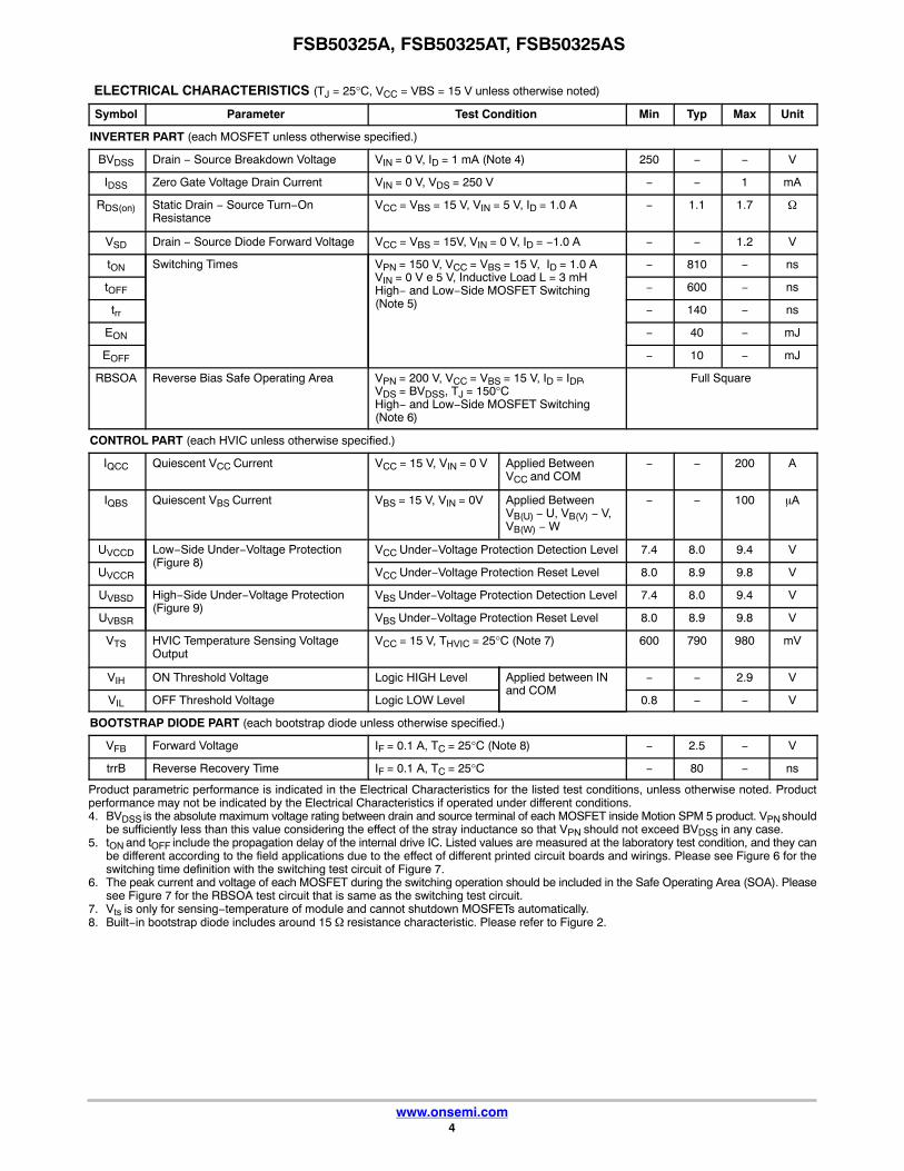
Tc = 25°C
00.0
0.1
0.2
0.3
0.4
0.5
0.6
0.7
0.8
0.9
1.0
1 2 3 4 5 6 7 8 9 10 11 12 13 14 15
Built−in Bootstrap Diode VF − IF Characteristic
I F [A
]
VF [V]
Figure 2. Built−in Bootstrap Diode Characteristics (Typical)
COM
VCC
LIN
HIN
VB
HO
VS
LO
P
N R3
InverterOutput
C3
C1
MC
U
+15 V
R5
C5
VDC
C2
VTS
* Example Circuit : V phase
C4
V
One Leg Diagram of Motion SPM 5 Product
These values depend on PWM control algorithm
10 μF
* Example of Bootstrap Parameters
C1 = C2 = 1 �F Ceramic Capacitor
HIN LIN Output Note
0 0 Z Both FRFET Off
0 1 0 Low side FRFET On
1 0 VDC High side FRFET On
1 1 Forbidden Shoot through
Open Open Z Same as (0, 0)
Figure 3. Recommended MCU Interface and Bootstrap Circuit with Parameters
NOTES:9. Parameters for bootstrap circuit elements are dependent on PWM algorithm. For 15 kHz of switching frequency, typical example of
parameters is shown above.10.RC−coupling (R5 and C5) and C4 at each input of Motion SPM 5 product and MCU (Indicated as Dotted Lines) may be used to prevent
improper signal due to surge−noise.11. Bold lines should be short and thick in PCB pattern to have small stray inductance of circuit, which results in the reduction of surge−voltage.
Bypass capacitors such as C1, C2 and C3 should have good high−frequency characteristics to absorb high−frequency ripple−current.
FSB50325A, FSB50325AT, FSB50325AS
www.onsemi.com6
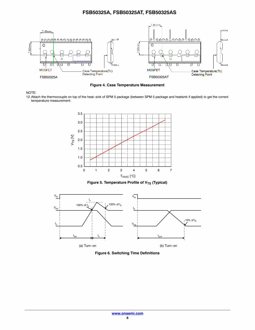
FSB50325A FSB50325AT
Figure 4. Case Temperature Measurement
NOTE:12.Attach the thermocouple on top of the heat−sink of SPM 5 package (between SPM 5 package and heatsink if applied) to get the correct
temperature measurement.
Figure 5. Temperature Profile of VTS (Typical)
0.5
1.0
1.5
2.0
2.5
3.0
3.5
0 1 2 3 4 5 6 7
VT
S [V
]
THVIC [°C]
tON trr
Irr
100% of ID120% of ID
tOFF
ID
VDS
VDS
ID
VIN VIN
10% of ID
(a) Turn−on (b) Turn−on
Figure 6. Switching Time Definitions

FSB50325A, FSB50325AT, FSB50325AS
www.onsemi.com7
COM
VCC
LIN
HIN
VB
HO
VS
LO
IDVCC
CBS
L DC
+VDS−VTS
One Leg Diagram of Motion SPM 5 Product
V
Figure 7. Switching and RBSOA (Single−pulse) Test Circuit (Low−side)
Figure 8. Under−Voltage Protection (Low−Side)
Figure 9. Under−Voltage Protection (High−Side)
UVCCD
UVCCR
Input Signal
UV ProtectionStatus
Low−side Supply, VCC
MOSFET Current
RESET DETECTION RESET
UVBSD
UVBSR
Input Signal
UV ProtectionStatus
High−side Supply, V BS
MOSFET Current
RESET DETECTION RESET
FSB50325A, FSB50325AT, FSB50325AS
www.onsemi.com8
COM
VCC
LIN
HIN
VB
HO
COM
VCC
LIN
HIN
COM
VCC
LIN
HIN
VB
HO
(1) COM
(2) V B(U)
(3) VCC(U)
(4) IN(UH)
(5) IN(UL)
(6) N.C
(7) V B(V)
(8) VCC(V)
(9) IN(VH)
(10) IN(VL)
(11) VTS
(12) VB(W)
(13) VCC(W)
(14) IN(WH)
(15) IN(WL)
(16) N.C
(17) P
(18) U, VS(U)
(19) NU
(22) NW
Mic
om
C1
15 VSupply
C3 VDC
C2
R3
R4
C6
R5
C5
For current−sensing and protection
V TS
(21) V, VS(V)
(20) NV
(23) W, VS(W)
C4
M
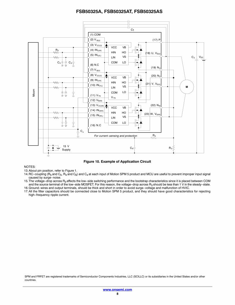
Figure 10. Example of Application Circuit
VB
HO
VS
LO
VS
LO
VS
LO
NOTES:13.About pin position, refer to Figure 1.14.RC−coupling (R5 and C5, R4 and C6) and C4 at each input of Motion SPM 5 product and MCU are useful to prevent improper input signal
caused by surge−noise.15.The voltage−drop across R3 affects the low−side switching performance and the bootstrap characteristics since it is placed between COM
and the source terminal of the low−side MOSFET. For this reason, the voltage−drop across R3 should be less than 1 V in the steady−state.16.Ground−wires and output terminals, should be thick and short in order to avoid surge−voltage and malfunction of HVIC.17.All the filter capacitors should be connected close to Motion SPM 5 product, and they should have good characteristics for rejecting
high−frequency ripple current.
SPM and FRFET are registered trademarks of Semiconductor Components Industries, LLC (SCILLC) or its subsidiaries in the United States and/or othercountries.
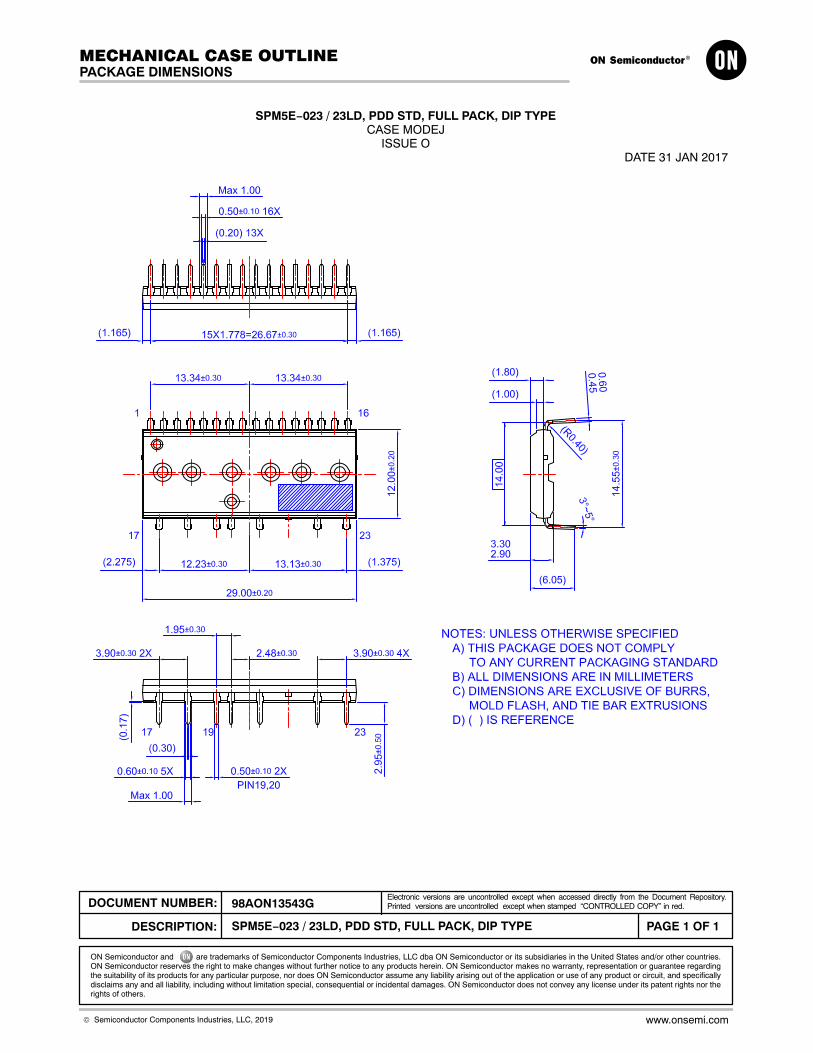
SPM5E−023 / 23LD, PDD STD, FULL PACK, DIP TYPECASE MODEJ
ISSUE ODATE 31 JAN 2017
MECHANICAL CASE OUTLINE
PACKAGE DIMENSIONS
ON Semiconductor and are trademarks of Semiconductor Components Industries, LLC dba ON Semiconductor or its subsidiaries in the United States and/or other countries.ON Semiconductor reserves the right to make changes without further notice to any products herein. ON Semiconductor makes no warranty, representation or guarantee regardingthe suitability of its products for any particular purpose, nor does ON Semiconductor assume any liability arising out of the application or use of any product or circuit, and specificallydisclaims any and all liability, including without limitation special, consequential or incidental damages. ON Semiconductor does not convey any license under its patent rights nor therights of others.
98AON13543GDOCUMENT NUMBER:
DESCRIPTION:
Electronic versions are uncontrolled except when accessed directly from the Document Repository.Printed versions are uncontrolled except when stamped “CONTROLLED COPY” in red.
PAGE 1 OF 1SPM5E−023 / 23LD, PDD STD, FULL PACK, DIP TYPE
© Semiconductor Components Industries, LLC, 2019 www.onsemi.com
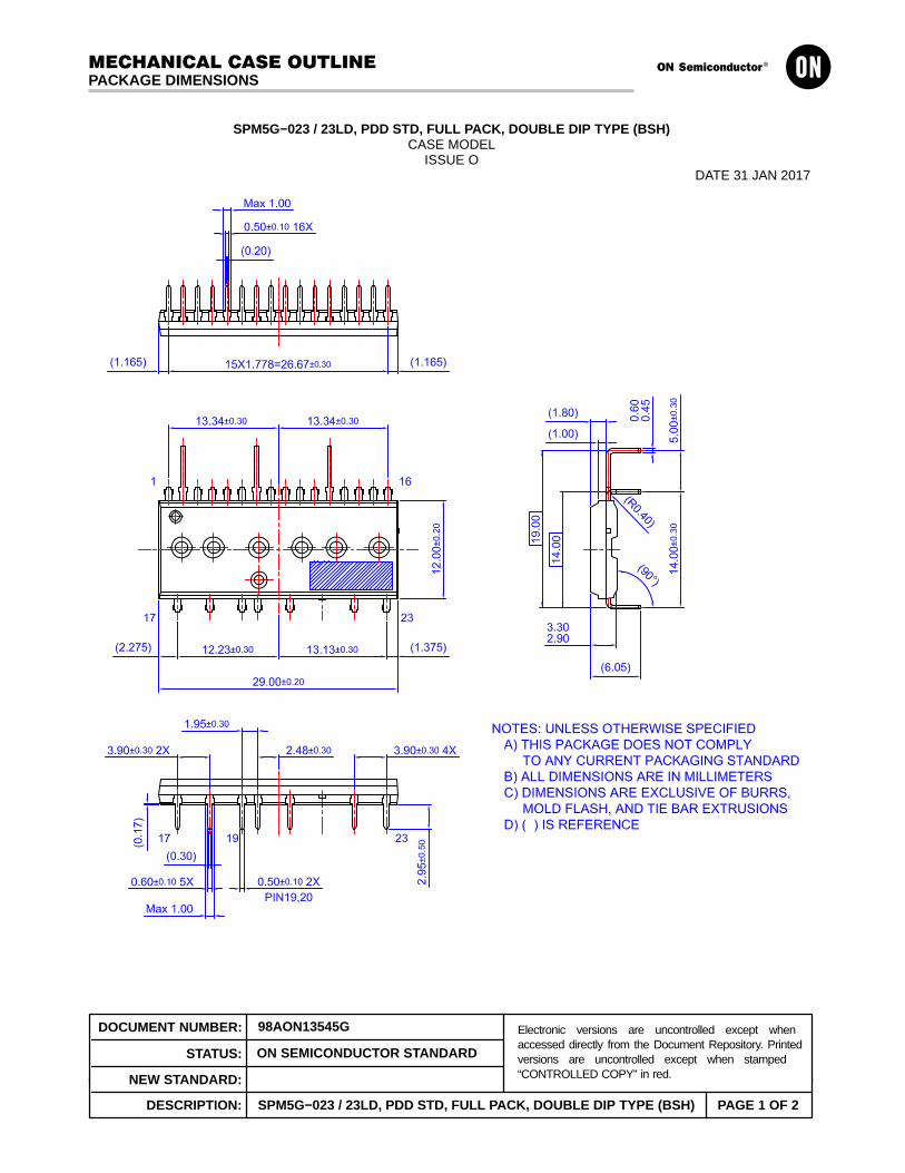
SPM5G−023 / 23LD, PDD STD, FULL PACK, DOUBLE DIP TYPE (BSH)CASE MODEL
ISSUE ODATE 31 JAN 2017
MECHANICAL CASE OUTLINE
PACKAGE DIMENSIONS
http://onsemi.com1
© Semiconductor Components Industries, LLC, 2002
October, 2002 − Rev. 0Case Outline Number:
XXX
DOCUMENT NUMBER:
STATUS:
NEW STANDARD:
DESCRIPTION:
98AON13545G
ON SEMICONDUCTOR STANDARD
SPM5G−023 / 23LD, PDD STD, FULL PACK, DOUBLE DIP TYPE (BSH)
Electronic versions are uncontrolled except when accessed directly from the Document Repository. Printed versions are uncontrolled except when stamped “CONTROLLED COPY” in red.
PAGE 1 OF 2

DOCUMENT NUMBER:98AON13545G
PAGE 2 OF 2
ISSUE REVISION DATE
O RELEASED FOR PRODUCTION FROM FAIRCHILD MOD23DF TO ON SEMICON-DUCTOR. REQ. BY D. GASTELUM.
31 JAN 2017
© Semiconductor Components Industries, LLC, 2017
January, 2017 − Rev. OCase Outline Number:
MODEL
ON Semiconductor and are registered trademarks of Semiconductor Components Industries, LLC (SCILLC). SCILLC reserves the right to make changes without further noticeto any products herein. SCILLC makes no warranty, representation or guarantee regarding the suitability of its products for any particular purpose, nor does SCILLC assume any liabilityarising out of the application or use of any product or circuit, and specifically disclaims any and all liability, including without limitation special, consequential or incidental damages.“Typical” parameters which may be provided in SCILLC data sheets and/or specifications can and do vary in different applications and actual performance may vary over time. Alloperating parameters, including “Typicals” must be validated for each customer application by customer’s technical experts. SCILLC does not convey any license under its patent rightsnor the rights of others. SCILLC products are not designed, intended, or authorized for use as components in systems intended for surgical implant into the body, or other applicationsintended to support or sustain life, or for any other application in which the failure of the SCILLC product could create a situation where personal injury or death may occur. ShouldBuyer purchase or use SCILLC products for any such unintended or unauthorized application, Buyer shall indemnify and hold SCILLC and its officers, employees, subsidiaries, affiliates,and distributors harmless against all claims, costs, damages, and expenses, and reasonable attorney fees arising out of, directly or indirectly, any claim of personal injury or deathassociated with such unintended or unauthorized use, even if such claim alleges that SCILLC was negligent regarding the design or manufacture of the part. SCILLC is an EqualOpportunity/Affirmative Action Employer. This literature is subject to all applicable copyright laws and is not for resale in any manner.
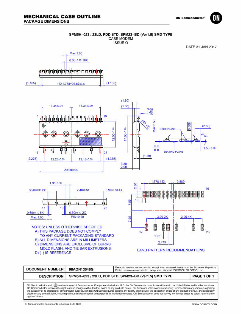
SPM5H−023 / 23LD, PDD STD, SPM23−BD (Ver1.5) SMD TYPECASE MODEM
ISSUE ODATE 31 JAN 2017
MECHANICAL CASE OUTLINE
PACKAGE DIMENSIONS
ON Semiconductor and are trademarks of Semiconductor Components Industries, LLC dba ON Semiconductor or its subsidiaries in the United States and/or other countries.ON Semiconductor reserves the right to make changes without further notice to any products herein. ON Semiconductor makes no warranty, representation or guarantee regardingthe suitability of its products for any particular purpose, nor does ON Semiconductor assume any liability arising out of the application or use of any product or circuit, and specificallydisclaims any and all liability, including without limitation special, consequential or incidental damages. ON Semiconductor does not convey any license under its patent rights nor therights of others.
98AON13546GDOCUMENT NUMBER:
DESCRIPTION:
Electronic versions are uncontrolled except when accessed directly from the Document Repository.Printed versions are uncontrolled except when stamped “CONTROLLED COPY” in red.
PAGE 1 OF 1SPM5H−023 / 23LD, PDD STD, SPM23−BD (Ver1.5) SMD TYPE
© Semiconductor Components Industries, LLC, 2019 www.onsemi.com
onsemi, , and other names, marks, and brands are registered and/or common law trademarks of Semiconductor Components Industries, LLC dba “onsemi” or its affiliatesand/or subsidiaries in the United States and/or other countries. onsemi owns the rights to a number of patents, trademarks, copyrights, trade secrets, and other intellectual property.A listing of onsemi’s product/patent coverage may be accessed at www.onsemi.com/site/pdf/Patent−Marking.pdf. onsemi reserves the right to make changes at any time to anyproducts or information herein, without notice. The information herein is provided “as−is” and onsemi makes no warranty, representation or guarantee regarding the accuracy of theinformation, product features, availability, functionality, or suitability of its products for any particular purpose, nor does onsemi assume any liability arising out of the application or useof any product or circuit, and specifically disclaims any and all liability, including without limitation special, consequential or incidental damages. Buyer is responsible for its productsand applications using onsemi products, including compliance with all laws, regulations and safety requirements or standards, regardless of any support or applications informationprovided by onsemi. “Typical” parameters which may be provided in onsemi data sheets and/or specifications can and do vary in different applications and actual performance mayvary over time. All operating parameters, including “Typicals” must be validated for each customer application by customer’s technical experts. onsemi does not convey any licenseunder any of its intellectual property rights nor the rights of others. onsemi products are not designed, intended, or authorized for use as a critical component in life support systemsor any FDA Class 3 medical devices or medical devices with a same or similar classification in a foreign jurisdiction or any devices intended for implantation in the human body. ShouldBuyer purchase or use onsemi products for any such unintended or unauthorized application, Buyer shall indemnify and hold onsemi and its officers, employees, subsidiaries, affiliates,and distributors harmless against all claims, costs, damages, and expenses, and reasonable attorney fees arising out of, directly or indirectly, any claim of personal injury or deathassociated with such unintended or unauthorized use, even if such claim alleges that onsemi was negligent regarding the design or manufacture of the part. onsemi is an EqualOpportunity/Affirmative Action Employer. This literature is subject to all applicable copyright laws and is not for resale in any manner.
PUBLICATION ORDERING INFORMATIONTECHNICAL SUPPORTNorth American Technical Support:Voice Mail: 1 800−282−9855 Toll Free USA/CanadaPhone: 011 421 33 790 2910
LITERATURE FULFILLMENT:Email Requests to: [email protected]
onsemi Website: www.onsemi.com
Europe, Middle East and Africa Technical Support:Phone: 00421 33 790 2910For additional information, please contact your local Sales Representative
◊