fsbs10ch60 motion spm® 3 series - farnell element14 · 2013. 9. 12. · fsbs10ch60 rev. c03...
TRANSCRIPT
©2005 Fairchild Semiconductor Corporation 1 www.fairchildsemi.com
FSBS10CH60 Rev. C03
FSBS10CH60 M
otio
n SPM® 3 Serie
s
March 2013
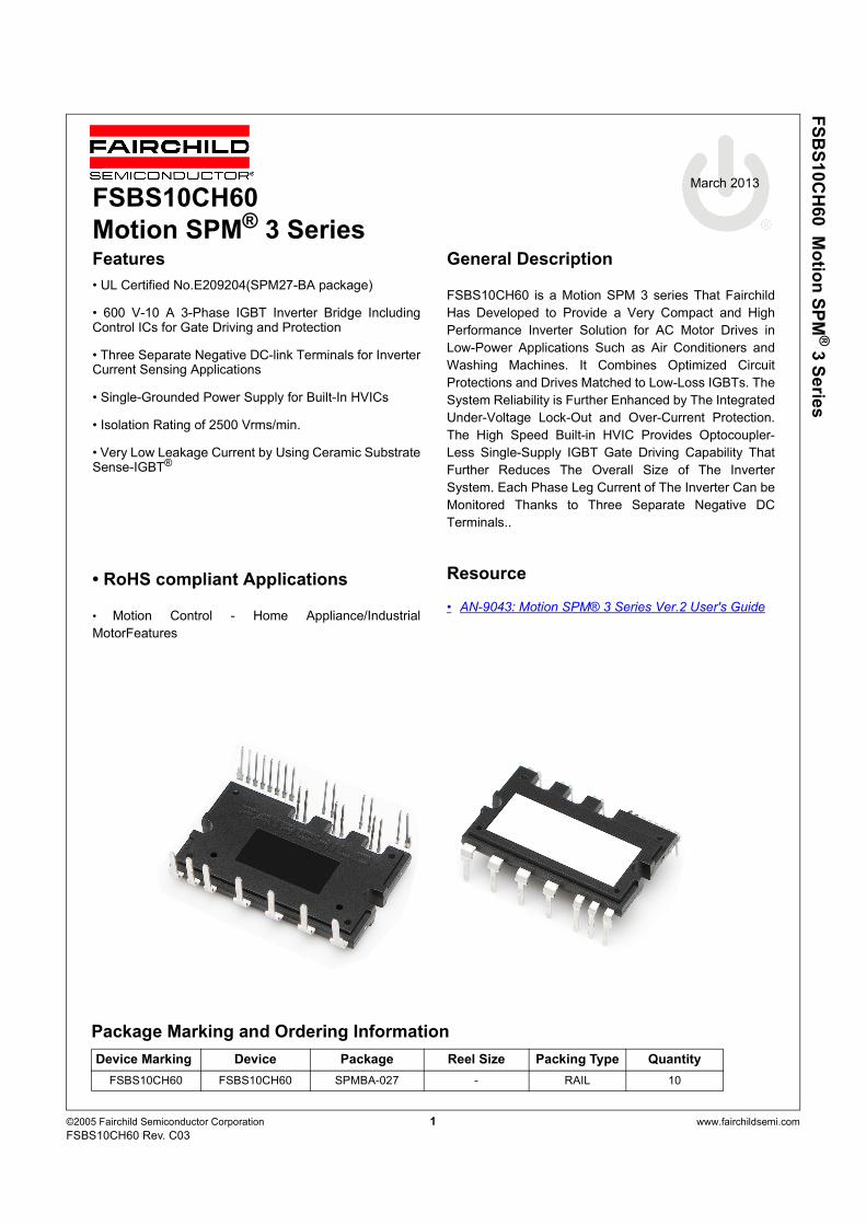
FSBS10CH60
Motion SPM® 3 SeriesFeatures
• UL Certified No.E209204(SPM27-BA package)
• 600 V-10 A 3-Phase IGBT Inverter Bridge IncludingControl ICs for Gate Driving and Protection
• Three Separate Negative DC-link Terminals for InverterCurrent Sensing Applications
• Single-Grounded Power Supply for Built-In HVICs
• Isolation Rating of 2500 Vrms/min.
• Very Low Leakage Current by Using Ceramic SubstrateSense-IGBT®
• RoHS compliant Applications
• Motion Control - Home Appliance/Industrial
MotorFeatures
General Description
FSBS10CH60 is a Motion SPM 3 series That Fairchild
Has Developed to Provide a Very Compact and High
Performance Inverter Solution for AC Motor Drives in
Low-Power Applications Such as Air Conditioners and
Washing Machines. It Combines Optimized Circuit
Protections and Drives Matched to Low-Loss IGBTs. The
System Reliability is Further Enhanced by The Integrated
Under-Voltage Lock-Out and Over-Current Protection.
The High Speed Built-in HVIC Provides Optocoupler-
Less Single-Supply IGBT Gate Driving Capability That
Further Reduces The Overall Size of The Inverter
System. Each Phase Leg Current of The Inverter Can be
Monitored Thanks to Three Separate Negative DC
Terminals..
Resource
• AN-9043: Motion SPM® 3 Series Ver.2 User's Guide
Package Marking and Ordering Information
Device Marking Device Package Reel Size Packing Type Quantity
FSBS10CH60 FSBS10CH60 SPMBA-027 - RAIL 10
FSBS10CH60 M
otio
n SPM® 3 Serie
s
©2005 Fairchild Semiconductor Corporation 2 www.fairchildsemi.com
Integrated Power Functions
• 600 V-10 A IGBT Inverter for Three-Phase DC/AC Power Conversion (Please Refer to Figure 3)
Integrated Drive, Protection and System Control Functions
• For Inverter High-Side IGBTs: Gate Drive Circuit, High Voltage Isolated High-Speed Level Shifting
Control Circuit Under-Voltage (UV) Protection
Note) Available Bootstrap Circuit Example is Given in Figures 10 and 11.
• For Inverter Low-Side IGBTs: Gate Drive Circuit, Short Circuit Protection (SC)
Control Supply Circuit Under-Voltage (UV) Protection
• Fault Sgnaling: Corresponding to a UV Fault (Low-Side Supply)
• Input interface: Active - High Interface, Can Work with 3.3/5 V Logic
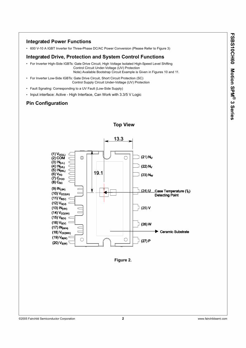
Pin Configuration
Figure 2.
(1) VCC(L)
(2) COM(3) IN(UL)
(4) IN(VL)
(5) IN(WL)
(6) VFO
(21) NU
(22) NV
(23) NW
(27) P
(15) VB(V)
(16) VS(V)
(17) IN(WH)
(18) VCC(WH)
(19) VB(W)
(20) VS(W)
(24) U
(25) V
(26) W
Case Temperature (TC)Detecting Point
Ceramic Substrate
(7) CFOD
(8) CSC
(9) IN(UH)
(10) VCC(UH)
(11) VB(U)
(12) VS(U)
(13) IN(VH)
(14) VCC(VH)
(1) VCC(L)
(2) COM(3) IN(UL)
(4) IN(VL)
(5) IN(WL)
(6) VFO
(21) NU
(22) NV
(23) NW
(27) P
(15) VB(V)
(16) VS(V)
(17) IN(WH)
(18) VCC(WH)
(19) VB(W)
(20) VS(W)
U
V
(26) W
Case Temperature (TC)Detecting Point
Ceramic Substrate
(7) CFOD
(8) CSC
(9) IN(UH)
(10) VCC(UH)
(11) VB(U)
(12) VS(U)
(13) IN(VH)
(14) VCC(VH)
13.3
19.1
(1) VCC(L)
(2) COM(3) IN(UL)
(4) IN(VL)
(5) IN(WL)
(6) VFO
(21) NU
(22) NV
(23) NW
(27) P
(15) VB(V)
(16) VS(V)
(17) IN(WH)
(18) VCC(WH)
(19) VB(W)
(20) VS(W)
(24) U
(25) V
(26) W
Case Temperature (TC)Detecting Point
Ceramic Substrate
(7) CFOD
(8) CSC
(9) IN(UH)
(10) VCC(UH)
(11) VB(U)
(12) VS(U)
(13) IN(VH)
(14) VCC(VH)
(1) VCC(L)
(2) COM(3) IN(UL)
(4) IN(VL)
(5) IN(WL)
(6) VFO
(21) NU
(22) NV
(23) NW
(27) P
(15) VB(V)
(16) VS(V)
(17) IN(WH)
(18) VCC(WH)
(19) VB(W)
(20) VS(W)
U
V
(26) W
Case Temperature (TC)Detecting Point
Ceramic Substrate
(7) CFOD
(8) CSC
(9) IN(UH)
(10) VCC(UH)
(11) VB(U)
(12) VS(U)
(13) IN(VH)
(14) VCC(VH)
13.3
19.1
13.3
19.1
Top View
FSBS10CH60 M
otio
n SPM® 3 Serie
s
©2005 Fairchild Semiconductor Corporation 3 www.fairchildsemi.com
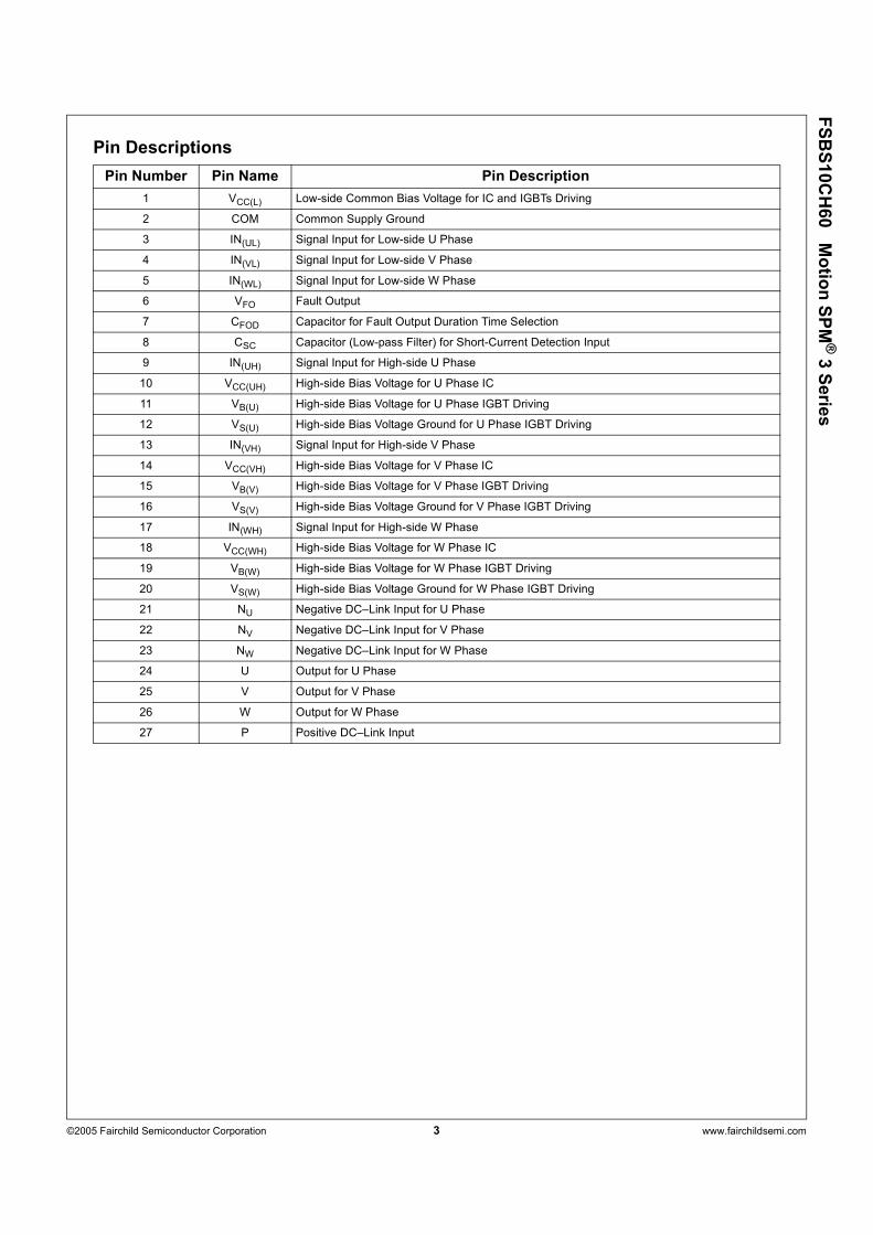
Pin Descriptions
Pin Number Pin Name Pin Description
1 VCC(L) Low-side Common Bias Voltage for IC and IGBTs Driving
2 COM Common Supply Ground
3 IN(UL) Signal Input for Low-side U Phase
4 IN(VL) Signal Input for Low-side V Phase
5 IN(WL) Signal Input for Low-side W Phase
6 VFO Fault Output
7 CFOD Capacitor for Fault Output Duration Time Selection
8 CSC Capacitor (Low-pass Filter) for Short-Current Detection Input
9 IN(UH) Signal Input for High-side U Phase
10 VCC(UH) High-side Bias Voltage for U Phase IC
11 VB(U) High-side Bias Voltage for U Phase IGBT Driving
12 VS(U) High-side Bias Voltage Ground for U Phase IGBT Driving
13 IN(VH) Signal Input for High-side V Phase
14 VCC(VH) High-side Bias Voltage for V Phase IC
15 VB(V) High-side Bias Voltage for V Phase IGBT Driving
16 VS(V) High-side Bias Voltage Ground for V Phase IGBT Driving
17 IN(WH) Signal Input for High-side W Phase
18 VCC(WH) High-side Bias Voltage for W Phase IC
19 VB(W) High-side Bias Voltage for W Phase IGBT Driving
20 VS(W) High-side Bias Voltage Ground for W Phase IGBT Driving
21 NU Negative DC–Link Input for U Phase
22 NV Negative DC–Link Input for V Phase
23 NW Negative DC–Link Input for W Phase
24 U Output for U Phase
25 V Output for V Phase
26 W Output for W Phase
27 P Positive DC–Link Input
FSBS10CH60 M
otio
n SPM® 3 Serie
s
©2005 Fairchild Semiconductor Corporation 4 www.fairchildsemi.com
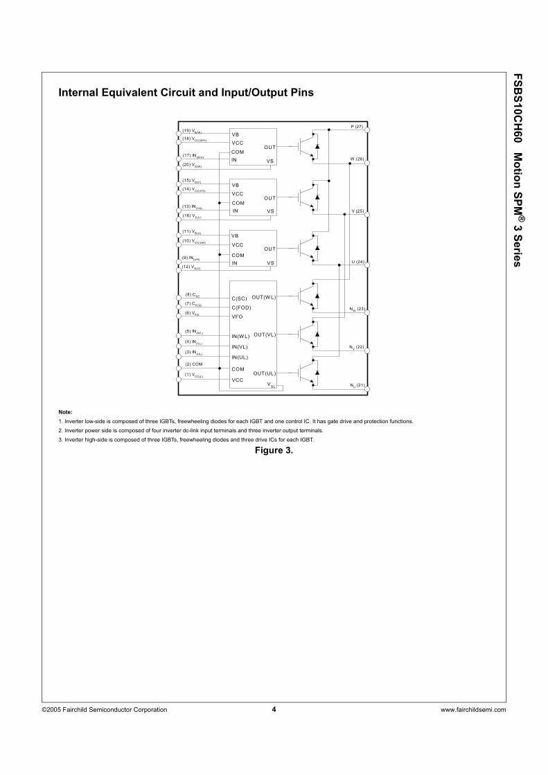
Internal Equivalent Circuit and Input/Output Pins
Note:
1. Inverter low-side is composed of three IGBTs, freewheeling diodes for each IGBT and one control IC. It has gate drive and protection functions.
2. Inverter power side is composed of four inverter dc-link input terminals and three inverter output terminals.
3. Inverter high-side is composed of three IGBTs, freewheeling diodes and three drive ICs for each IGBT.
Figure 3.
COM
VCC
IN(UL)
IN(VL)
IN(WL)
VFO
C(FOD)
C(SC)
OUT(UL)
OUT(VL)
OUT(W L)
NU (21)
NV (22)
NW (23)
U (24)
V (25)
W (26)
P (27)
(20) VS(W )
(19) VB(W )
(16) VS(V)
(15) VB(V)
(8) CSC
(7) CFOD
(6) VFO
(5) IN(WL)
(4) IN(VL)
(3) IN(UL)
(2) COM
(1) VCC(L)
VCC
VB
OUTCOM
VSIN
VB
VS
OUT
IN
COM
VCC
VCC
VB
OUTCOM
VSIN
(18) VCC(WH)
(17) IN(WH)
(14) VCC(VH)
(13) IN(VH)
(12) VS(U)
(11) VB(U)
(10) VCC(UH)
(9) IN(UH)
VSL
FSBS10CH60 M
otio
n SPM® 3 Serie
s
©2005 Fairchild Semiconductor Corporation 5 www.fairchildsemi.com
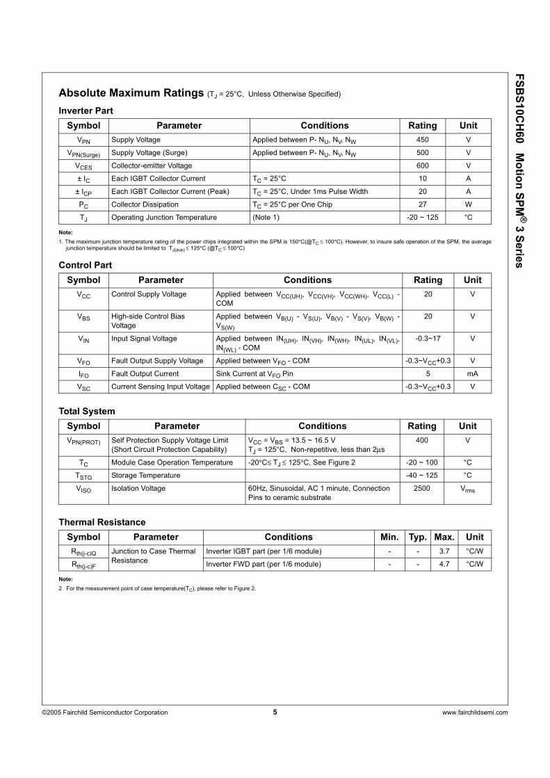
Absolute Maximum Ratings (TJ = 25°C, Unless Otherwise Specified)
Inverter Part
Note:
1. The maximum junction temperature rating of the power chips integrated within the SPM is 150°C(@TC ≤ 100°C). However, to insure safe operation of the SPM, the averagejunction temperature should be limited to TJ(ave) ≤ 125°C (@TC ≤ 100°C)
Control Part
Total System
Thermal Resistance
Note:
2. For the measurement point of case temperature(TC), please refer to Figure 2.
Symbol Parameter Conditions Rating Unit
VPN Supply Voltage Applied between P- NU, NV, NW 450 V
VPN(Surge) Supply Voltage (Surge) Applied between P- NU, NV, NW 500 V
VCES Collector-emitter Voltage 600 V
± IC Each IGBT Collector Current TC = 25°C 10 A
± ICP Each IGBT Collector Current (Peak) TC = 25°C, Under 1ms Pulse Width 20 A
PC Collector Dissipation TC = 25°C per One Chip 27 W
TJ Operating Junction Temperature (Note 1) -20 ~ 125 °C
Symbol Parameter Conditions Rating Unit
VCC Control Supply Voltage Applied between VCC(UH), VCC(VH), VCC(WH), VCC(L) -
COM
20 V
VBS High-side Control Bias
Voltage
Applied between VB(U) - VS(U), VB(V) - VS(V), VB(W) -
VS(W)
20 V
VIN Input Signal Voltage Applied between IN(UH), IN(VH), IN(WH), IN(UL), IN(VL),
IN(WL) - COM
-0.3~17 V
VFO Fault Output Supply Voltage Applied between VFO - COM -0.3~VCC+0.3 V
IFO Fault Output Current Sink Current at VFO Pin 5 mA
VSC Current Sensing Input Voltage Applied between CSC - COM -0.3~VCC+0.3 V
Symbol Parameter Conditions Rating Unit
VPN(PROT) Self Protection Supply Voltage Limit
(Short Circuit Protection Capability)
VCC = VBS = 13.5 ~ 16.5 V
TJ = 125°C, Non-repetitive, less than 2µs
400 V
TC Module Case Operation Temperature -20°C≤ TJ ≤ 125°C, See Figure 2 -20 ~ 100 °C
TSTG Storage Temperature -40 ~ 125 °C
VISO Isolation Voltage 60Hz, Sinusoidal, AC 1 minute, Connection
Pins to ceramic substrate
2500 Vrms
Symbol Parameter Conditions Min. Typ. Max. Unit
Rth(j-c)Q Junction to Case Thermal
Resistance
Inverter IGBT part (per 1/6 module) - - 3.7 °C/W
Rth(j-c)F Inverter FWD part (per 1/6 module) - - 4.7 °C/W
FSBS10CH60 M
otio
n SPM® 3 Serie
s
©2005 Fairchild Semiconductor Corporation 6 www.fairchildsemi.com
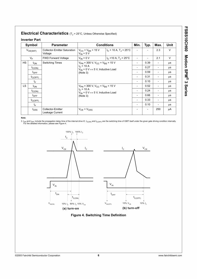
Electrical Characteristics (TJ = 25°C, Unless Otherwise Specified)
Inverter Part
Note:
3. tON and tOFF include the propagation delay time of the internal drive IC. tC(ON) and tC(OFF) are the switching time of IGBT itself under the given gate driving condition internally.For the detailed information, please see Figure 4.
Figure 4. Switching Time Definition
Symbol Parameter Conditions Min. Typ. Max. Unit
VCE(SAT) Collector-Emitter Saturation
Voltage
VCC = VBS = 15 V
VIN = 5 V
IC = 10 A, TJ = 25°C - - 2.3 V
VF FWD Forward Voltage VIN = 0 V IC =10 A, TJ = 25°C - - 2.1 V
HS tON Switching Times VPN = 300 V, VCC = VBS = 15 V
IC = 10 A
VIN = 0 V ↔ 5 V, Inductive Load
(Note 3)
- 0.39 - µs
tC(ON) - 0.27 - µs
tOFF - 0.59 - µs
tC(OFF) - 0.31 - µs
trr - 0.10 - µs
LS tON VPN = 300 V, VCC = VBS = 15 V
IC = 10 A
VIN = 0 V ↔ 5 V, Inductive Load
(Note 3)
- 0.52 - µs
tC(ON) - 0.24 - µs
tOFF - 0.66 - µs
tC(OFF) - 0.33 - µs
trr - 0.10 - µs
ICES Collector-Emitter
Leakage Current
VCE = VCES - - 250 µA
VCE
IC
VIN
tON
tC(ON)
VIN(ON) 10% I
C10% V
CE90% I
C
100% IC
trr
100% IC
0
VCE
IC
VIN
tOFF
tC(OFF)
VIN(OFF)
10% VCE
10% IC
(a) turn-on (b) turn-off
FSBS10CH60 M
otio
n SPM® 3 Serie
s
©2005 Fairchild Semiconductor Corporation 7 www.fairchildsemi.com
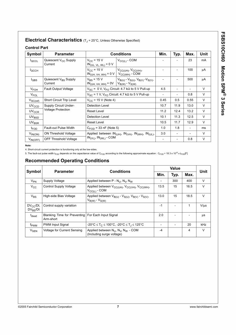
Electrical Characteristics (TJ = 25°C, Unless Otherwise Specified)
Control Part
Note:
4. Short-circuit current protection is functioning only at the low-sides.
5. The fault-out pulse width tFOD depends on the capacitance value of CFOD according to the following approximate equation : CFOD = 18.3 x 10⁻⁶ x tFOD[F]
Recommended Operating Conditions
Symbol Parameter Conditions Min. Typ. Max. Unit
IQCCL Quiescent VCC Supply
Current
VCC = 15 V
IN(UL, VL, WL) = 0 V
VCC(L) - COM - - 23 mA
IQCCH VCC = 15 V
IN(UH, VH, WH) = 0 V
VCC(UH), VCC(VH),
VCC(WH) - COM
- - 100 µA
IQBS Quiescent VBS Supply
Current
VBS = 15 V
IN(UH, VH, WH) = 0V
VB(U) - VS(U), VB(V) -VS(V),
VB(W) - VS(W)
- - 500 µA
VFOH Fault Output Voltage VSC = 0 V, VFO Circuit: 4.7 kΩ to 5 V Pull-up 4.5 - - V
VFOL VSC = 1 V, VFO Circuit: 4.7 kΩ to 5 V Pull-up - - 0.8 V
VSC(ref) Short Circuit Trip Level VCC = 15 V (Note 4) 0.45 0.5 0.55 V
UVCCD Supply Circuit Under-
Voltage Protection
Detection Level 10.7 11.9 13.0 V
UVCCR Reset Level 11.2 12.4 13.2 V
UVBSD Detection Level 10.1 11.3 12.5 V
UVBSR Reset Level 10.5 11.7 12.9 V
tFOD Fault-out Pulse Width CFOD = 33 nF (Note 5) 1.0 1.8 - ms
VIN(ON) ON Threshold Voltage Applied between IN(UH), IN(VH), IN(WH), IN(UL),
IN(VL), IN(WL) - COM
3.0 - - V
VIN(OFF) OFF Threshold Voltage - - 0.8 V
Symbol Parameter ConditionsValue
UnitMin. Typ. Max.
VPN Supply Voltage Applied between P - NU, NV, NW - 300 400 V
VCC Control Supply Voltage Applied between VCC(UH), VCC(VH), VCC(WH),
VCC(L) - COM
13.5 15 16.5 V
VBS High-side Bias Voltage Applied between VB(U) - VS(U), VB(V) - VS(V),
VB(W) - VS(W)
13.0 15 18.5 V
DVCC/Dt,
DVBS/Dt
Control supply variation -1 - 1 V/µs
tdead Blanking Time for Preventing
Arm-short
For Each Input Signal 2.0 - - µs
fPWM PWM Input Signal -20°C ≤ TC ≤ 100°C, -20°C ≤ TJ ≤ 125°C - - 20 kHz
VSEN Voltage for Current Sensing Applied between NU, NV, NW - COM
(Including surge voltage)
-4 4 V
FSBS10CH60 M
otio
n SPM® 3 Serie
s
©2005 Fairchild Semiconductor Corporation 8 www.fairchildsemi.com
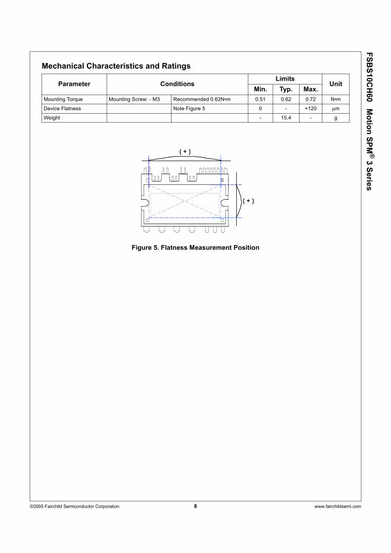
Mechanical Characteristics and Ratings
Figure 5. Flatness Measurement Position
Parameter ConditionsLimits
UnitMin. Typ. Max.
Mounting Torque Mounting Screw: - M3 Recommended 0.62N•m 0.51 0.62 0.72 N•m
Device Flatness Note Figure 5 0 - +120 µm
Weight - 15.4 - g
( + )
( + )
( + )
( + )
FSBS10CH60 M
otio
n SPM® 3 Serie
s
©2005 Fairchild Semiconductor Corporation 9 www.fairchildsemi.com
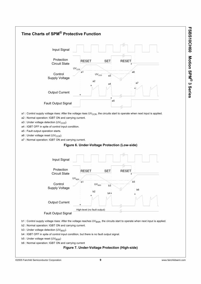
Time Charts of SPM® Protective Function
a1 : Control supply voltage rises: After the voltage rises UVCCR, the circuits start to operate when next input is applied.
a2 : Normal operation: IGBT ON and carrying current.
a3 : Under voltage detection (UVCCD).
a4 : IGBT OFF in spite of control input condition.
a5 : Fault output operation starts.
a6 : Under voltage reset (UVCCR).
a7 : Normal operation: IGBT ON and carrying current.
Figure 6. Under-Voltage Protection (Low-side)
b1 : Control supply voltage rises: After the voltage reaches UVBSR, the circuits start to operate when next input is applied.
b2 : Normal operation: IGBT ON and carrying current.
b3 : Under voltage detection (UVBSD).
b4 : IGBT OFF in spite of control input condition, but there is no fault output signal.
b5 : Under voltage reset (UVBSR)
b6 : Normal operation: IGBT ON and carrying current
Figure 7. Under-Voltage Protection (High-side)
Input Signal
Output Current
Fault Output Signal
Control
Supply Voltage
RESET
UVCCR
Protection
Circuit StateSET RESET
UVCCD
a1
a3
a2a4
a6
a5
a7
Input Signal
Output Current
Fault Output Signal
Control
Supply Voltage
RESET
UVBSR
Protection
Circuit StateSET RESET
UVBSD
b1
b3
b2b4
b6
b5
High-level (no fault output)
FSBS10CH60 M
otio
n SPM® 3 Serie
s
©2005 Fairchild Semiconductor Corporation 10 www.fairchildsemi.com
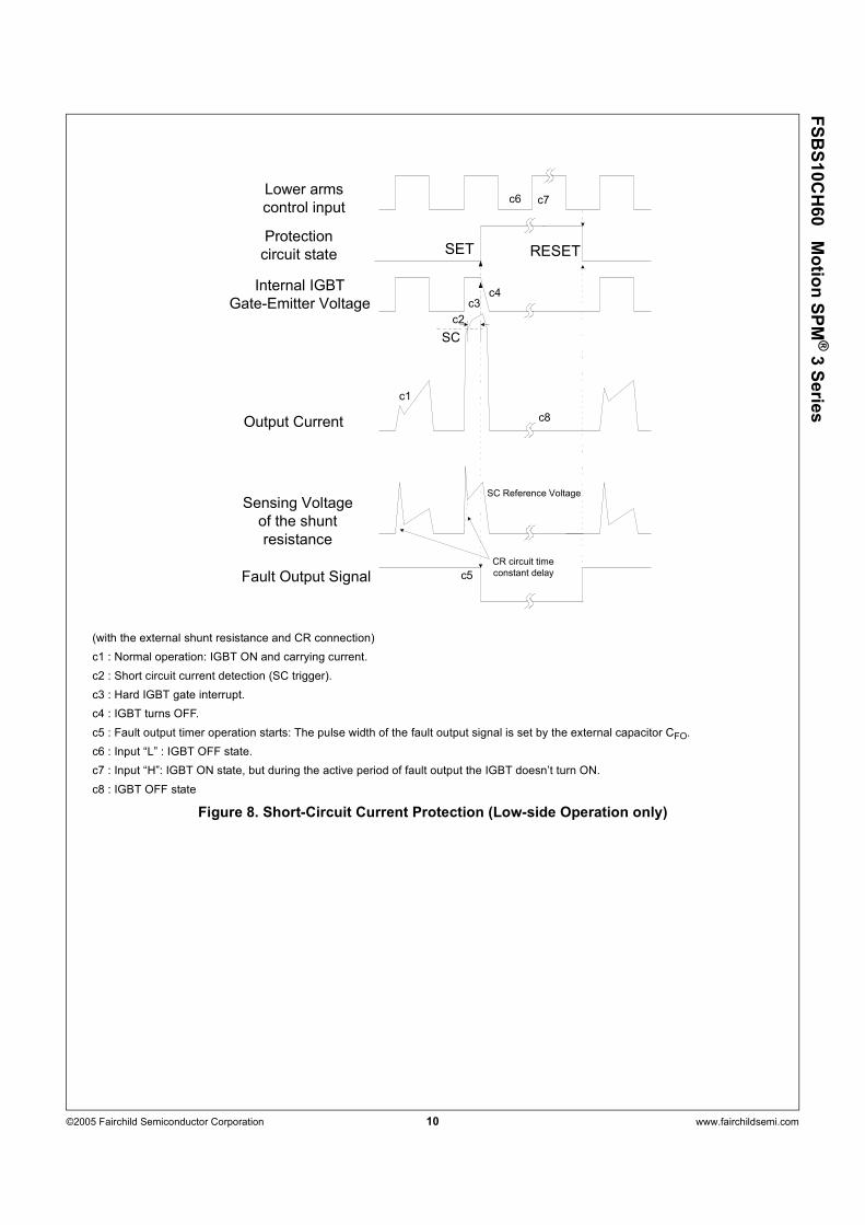
(with the external shunt resistance and CR connection)
c1 : Normal operation: IGBT ON and carrying current.
c2 : Short circuit current detection (SC trigger).
c3 : Hard IGBT gate interrupt.
c4 : IGBT turns OFF.
c5 : Fault output timer operation starts: The pulse width of the fault output signal is set by the external capacitor CFO.
c6 : Input “L” : IGBT OFF state.
c7 : Input “H”: IGBT ON state, but during the active period of fault output the IGBT doesn’t turn ON.
c8 : IGBT OFF state
Figure 8. Short-Circuit Current Protection (Low-side Operation only)
Internal IGBT
Gate-Emitter Voltage
Lower arms
control input
Output Current
Sensing Voltage
of the shunt
resistance
Fault Output Signal
SC Reference Voltage
CR circuit time
constant delay
SC
Protection
circuit state SET RESET
c6 c7
c3
c2
c1
c8
c4
c5
FSBS10CH60 M
otio
n SPM® 3 Serie
s
©2005 Fairchild Semiconductor Corporation 11 www.fairchildsemi.com
Note:
1. RC coupling at each input (parts shown dotted) might change depending on the PWM control scheme used in the application and the wiring impedance of the application’sprinted circuit board. The SPM input signal section integrates 3.3kΩ (typ.) pull-down resistor. Therefore, when using an external filtering resistor, please pay attention to the sig-nal voltage drop at input terminal.
2. The logic input is compatible with standard CMOS or LSTTL outputs.
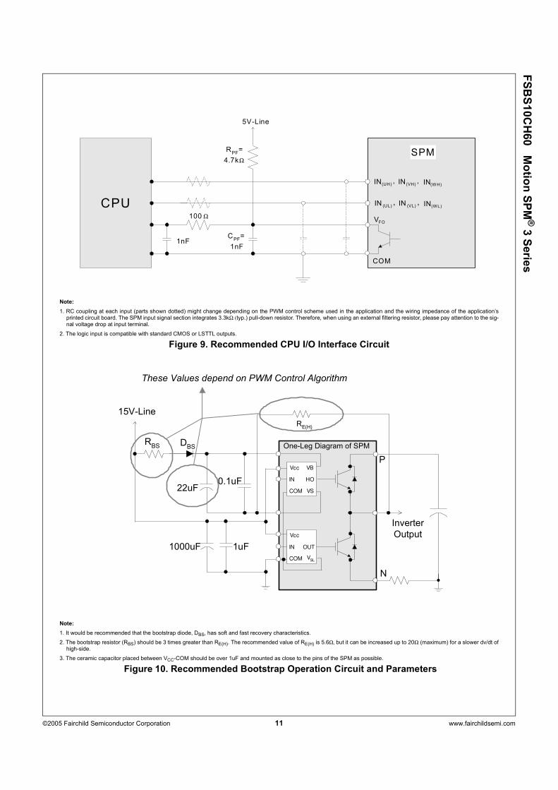
Figure 9. Recommended CPU I/O Interface Circuit
Note:
1. It would be recommended that the bootstrap diode, DBS, has soft and fast recovery characteristics.
2. The bootstrap resistor (RBS) should be 3 times greater than RE(H). The recommended value of RE(H) is 5.6Ω, but it can be increased up to 20Ω (maximum) for a slower dv/dt ofhigh-side.
3. The ceramic capacitor placed between VCC-COM should be over 1uF and mounted as close to the pins of the SPM as possible.
Figure 10. Recommended Bootstrap Operation Circuit and Parameters
CPU
COM
5V-Line
1nF
Ω4.7k
, ,IN (UL) IN (VL) IN(WL)
, ,IN(UH) IN (VH) IN(WH)
VFO
Ω100
1nF
SPMRPF=
CPF=
15V-Line
22uF0.1uF
1000uF 1uF
One-Leg Diagram of SPM
Vcc
IN
COM
VB
HO
VS
Vcc
IN
COM
OUT
Inverter
Output
P
N
These Values depend on PWM Control Algorithm
DBS
RBS
RE(H)
VSL
FSBS10CH60 M
otio
n SPM® 3 Serie
s
©2005 Fairchild Semiconductor Corporation 12 www.fairchildsemi.com
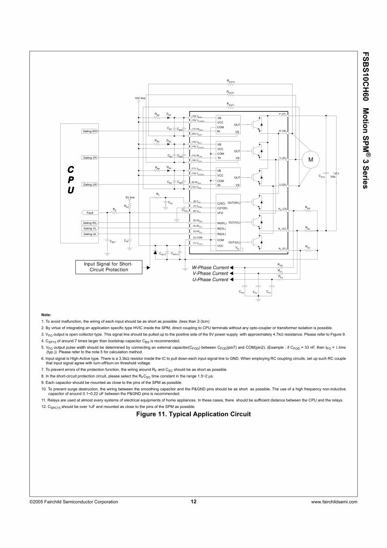
Note:
1. To avoid malfunction, the wiring of each input should be as short as possible. (less than 2-3cm)
2. By virtue of integrating an application specific type HVIC inside the SPM, direct coupling to CPU terminals without any opto-coupler or transformer isolation is possible.
3. VFO output is open collector type. This signal line should be pulled up to the positive side of the 5V power supply with approximately 4.7kΩ resistance. Please refer to Figure 9.
4. CSP15 of around 7 times larger than bootstrap capacitor CBS is recommended.
5. VFO output pulse width should be determined by connecting an external capacitor(CFOD) between CFOD(pin7) and COM(pin2). (Example : if CFOD = 33 nF, then tFO = 1.8ms(typ.)) Please refer to the note 5 for calculation method.
6. Input signal is High-Active type. There is a 3.3kΩ resistor inside the IC to pull down each input signal line to GND. When employing RC coupling circuits, set up such RC couplethat input signal agree with turn-off/turn-on threshold voltage.
7. To prevent errors of the protection function, the wiring around RF and CSC should be as short as possible.
8. In the short-circuit protection circuit, please select the RFCSC time constant in the range 1.5~2 µs.
9. Each capacitor should be mounted as close to the pins of the SPM as possible.
10. To prevent surge destruction, the wiring between the smoothing capacitor and the P&GND pins should be as short as possible. The use of a high frequency non-inductive
capacitor of around 0.1~0.22 uF between the P&GND pins is recommended.
11. Relays are used at almost every systems of electrical equipments of home appliances. In these cases, there should be sufficient distance between the CPU and the relays.
12. CSPC15 should be over 1uF and mounted as close to the pins of the SPM as possible.
Figure 11. Typical Application Circuit
Fault
15V line
CBS C
BSC
RBS
DBS
CBS
CBSC
RBS
DBS
CBS
CBSC
RBSD
BS
CSP15
CSPC15
CFOD
5V line
RPF
CBPF
RS
M
VdcCDCS
Gating UH
Gating VH
Gating WH
Gating WL
Gating VL
Gating UL
CPF
CCCC
PPPP
UUUU
RFU
RFV
RFW
RSU
RSV
RSW
CFUC
FVC
FW
W-Phase Current
V-Phase Current
U-Phase Current
RF
COM
VCC
IN(UL)
IN(VL)
IN(WL)
VFO
C(FOD)
C(SC)
OUT(UL)
OUT(VL)
OUT(WL)
NU (21)
NV (22)
NW (23)
U (24)
V (25)
W (26)
P (27)
(20) VS(W)
(19) VB(W)
(16) VS(V)
(15) VB(V)
(8) CSC
(7) CFOD
(6) VFO
(5) IN(WL)
(4) IN(VL)
(3) IN(UL)
(2) COM
(1) VCC(L)
VCC
VB
OUTCOM
VSIN
VB
VS
OUT
IN
COM
VCC
VCC
VB
OUTCOM
VSIN
(18) VCC(WH)
(17) IN(WH)
(14) VCC(VH)
(13) IN(VH)
(12) VS(U)
(11) VB(U)
(10) VCC(UH)
(9) IN(UH)
Input Signal for Short-Circuit Protection
CSC
RE(UH)
VSL
RE(VH)
RE(WH)
FSBS10CH60 M
otio
n SPM® 3 Serie
s
©2005 Fairchild Semiconductor Corporation 13 www.fairchildsemi.com
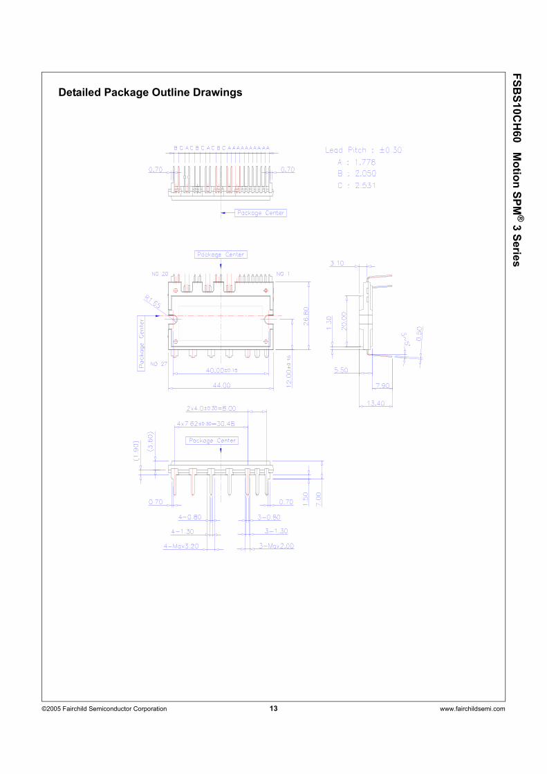
Detailed Package Outline Drawings
FSBS10CH60 M
otio
n SPM® 3 Serie
s
©2005 Fairchild Semiconductor Corporation 14 www.fairchildsemi.com
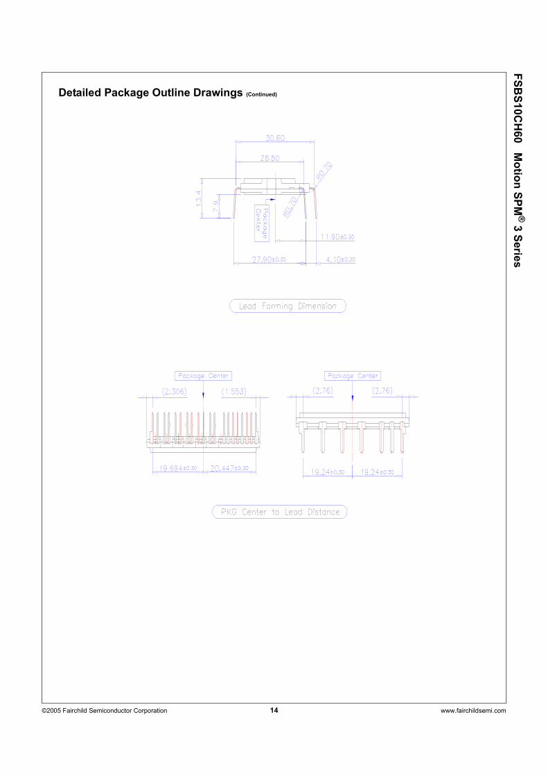
Detailed Package Outline Drawings (Continued)
FSBS10CH60 M
otio
n SPM® 3 Serie
s
©2005 Fairchild Semiconductor Corporation 15 www.fairchildsemi.com
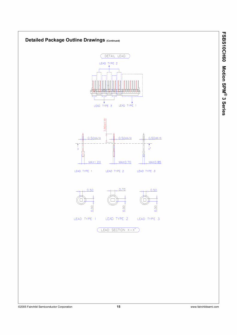
Detailed Package Outline Drawings (Continued)
FSBS10CH60 Motio
n SPM® 3 Serie
s
©2005 Fairchild Semiconductor Corporation 16 www.fairchildsemi.com