monolithic rf class-e power amplifier on cmos technologies · pdf filemonolithic rf class-e...
TRANSCRIPT

Monolithic RF Class-E power amplifier on CMOS technologies André Melo
Instituto Superior Técnico – campus Taguspark, Oeiras, Portugal e-mail: [email protected]
Abstract1— With the advancement of CMOS technology, the
trend is to design transceivers using this technology with the aim of achieving full integration and reduced system cost. The power amplifier (PA) being one of the most important blocks of the wireless communication system is no exception. The aim of this work is to provide the study that allow the design of a single-ended RF CMOS Class-E power amplifier for IEEE 802.11b / g applications. The technology that will be used to project the amplifier is UMC 0,18um CMOS. The main goal is to obtain a full integrated circuit with high efficiency to 2.4 GHz and output power exceeding 17 dBm. To design the various projects are used the common-source and cascode topology with and without driver stage. The drive projected is a class-F power amplifier tuned to the first and third harmonics.
I. INTRODUCTION
One of the main advantages of switched-mode power amplifier, class-E, is the possibility of having low voltage and high performance. At the same time, it presents less power losses for the same frequency. The class E doesn’t have many components, making it easier to obtain smaller circuit areas and more tolerance to variations in the fabrication process.
The class-E was presented by Erwing in 1964 in his PhD thesis [1] but it only got more attention in 1975, after the release of Nathan’s and Alan’s Sokal article [2]. Still in the 70’s, Raab [3] deepened the concept by proposing a few suggestions for an analysis of the amplifier in a more realistic way. Some years later a proposition for a new analysis method was made by [4], which presented one main difference when compared to Sokal’s: the premise that the drain inductance is finite. More recently, in 2006, Mustafa Acar [5] proposed another analyze, which presents simple design equation.
II. STATE-OF-THE-ART
The main motivation in RF power amplifiers investigation is based in the attempt to obtain a compromise between PAE, the ability to supply power and low consumption, in the many standards. As it will be widely discussed in this document, the class E amplifier is a strong candidate to fulfil these needs.
Although technologies exist that allow to obtain better results, like the ones that use GaAs and the SiGe, it was chosen to present in this sub-chapter only articles based on CMOS technology, since it’s considered to be a more fair comparison because. In spite of other technologies better performances, CMOS presents more relevance due to its low cost and potential integration.
The research made had as main focus, to synthesize the different options and respective results that different authors used. The first selection criteria used was to distinguish the main class E variants. In some cases differential topology is used and in other cases, single-ended. Within single-ended there’s a distinction between the classical approach (common-source switching) and the class E cascode (common-gate switching).
The authors that decided to use the differential mode to project class E [7][8], obtained an output power of 30 dBm and PAE of 62% and 48%, respectively. This approach is said to have as an advantage to reduce the coupling for the typical substract of the single-ended. It’s also said that for the same supply voltage and output power, the voltage that goes threw each switch is less than the total of losses in the switch. On the other hand, is necessary one additional interface to transform the differential signal into single-ended, since the majority of antennas need to be “excited” by a singe-ended signal. As described in [6], one of the many methods used to reduce substract coupling is the differential method which isn’t a very interesting option because it requires components external to the chip and increases the PA’s cost and makes it harder to fully integrate in a system. The obtained results don’t differ much from the rest, therefore not justifying the signalled advantage.
Using the single-ended mode (common-source switching), many articles exist with similar results. At 1.9 GHz the circuit [9] with higher PAE value was found, implemented in 0,18 um technology. This case is particularly interesting because besides an excellent PAE, it doesn’t need external components. A class-F power amplifier is used as drive. For the same frequency and technology of our work, there is a first case [10], from 2005, with results bellow the average (PAE = 40%) that uses external components. The other reported case [11] presents a higher PAE value but on the other hand a drive wasn’t implemented. In [11] the use of 0,18µm technology is pointed out as responsible for the god results obtained due to the considerably relevant factor of quality inductor. For the same frequency and technology from our work, this is the circuit that presents better performance.

For last, the class-E cascode topology (common-gate switching) is distinguished. For a frequency inferior to the one used in this work the article [12] was found, that represents the circuit with one of the better PAEs found, 67%. Meanwhile, the area occupied by this circuit is considered too big when compared to what other authors obtained. At the same frequency used in this work two articles were found, one [13] made in 0,35µm technology and the other [14] with the same technology, 0,18µm, used in this work. In the first case, the reasonable PAE obtained stands out (59%), and once again the choice for a class-F driver. In the second case, although presenting a PAE relatively low compared to the others the author managed to achieve a reasonable small area. All the authors using the class-E cascode justified that this configuration allows reducing the stress induced to the device. This parameter is particularly important since it allows reducing the voltage that the transistor is subdued (it can reach a level 2 or 3 times superior to the supply voltage) increasing the reliability of the device and it’s safety. A relevant negative aspect is that all authors had to recurred to external components.
Table 1 – State-of-the-art
III. CLASS-E
It is necessary to obtain RF power amplifier with high performance for certain applications as wireless communications as well as low consumption, justifying the use of class-E, as well as switching amplifiers in general. It becomes necessary to understand where the majority of power losses take place and try to minimize it. It’s known that some power losses take place in the capacitor and inductor, but in fact the higher loss of power is usually verified in the active device that functions as a switch. Is then important to know the best way to decrease the dissipated power. Ideally, there shouldn’t be any current and voltage passing threw the transistor at the same time. The opposite is also valid; being sometimes used the term non-overlapping current and voltage, which theoretically leads to a
performance of approximately 100% because there’s no dissipated power in the switch. In practice, the 100% performance is not achieved but there must be the concern of having the voltage and current waveforms as out of phase as possible, with a 50% duty-cycle, (figure 1), decreasing the existing time between high current values simultaneously with voltage and consequently decreasing the dissipated power and increasing it’s effectiveness. These conditions depend on the main network and are connected with the choice and dimension of the active device (switch) as well as the drive, giving place to voltage switch minimization when it’s “ON” and avoid current leaks when the switch is “OFF”. The concern to minimize the commutation time should also always be present, since it’s the time most likely to have voltage and current simultaneously in the active device.
Besides the conditions in displace, a class-E amplifier
should has a voltage-derived equal to zero when switching to the “ON” state (Zero Slope Voltage Switching, ZsVS). This particularity means that when the voltage that passes threw the transistor reaches zero, it’s derivative is approximately zero as well (1), In this way, the switching to the “ON” state can occur during a certain period of time without provoking a high power dissipation and consequent loss of performance, because it “coincide” with a low voltage value. Jointly with this condition, still in the switching for the “ON” state, the current should only start to run threw the switch when the voltage reaches the value zero - Zero Voltage Switching, ZVS. For the same reason, when the switch passes to the “OFF” state, the voltage should remain with a low value for a certain period of time, so that the current has time to reach zero - Zero Current Switching, ZCS – and only after this moment should it be increased to the desired value. These
Frequency
(GHz)
Technology
(µm)
Output power (dBm)
PAE (%)
[7] 0,7 0,35 30,0 62
[12] 1,7 0,13 23 67
[8] 1,9 0,35 30,0 48
[9] 1,9 0,18 16,3 70
[13] 2,4 0,35 20 59
[14] 2,4 0,18 23 44,5
[10] 2,4 0,18 21,3 40
[11] 2,4 0,18 17,3 63
Figure 1 - Current and voltage waveform for maximum efficiency. Adapted from [2]

characteristics are dependant on the temporal response of the output network.
𝑑𝑣𝑑𝑡
≈ 0 (1)
During many times the RF PAs were implemented in other
technologies with GaAs or SiGe subtracts essentially because of the few losses in the switch, which is important for the switching amplifiers. So, in the implementation of the class E amplifier in CMOS is important to have a switch with few losses for the desired frequency, which isn’t always easy due to the low resistance of the “ON” state, compromising the necessity of having a high performance. As it regards to the passive elements, sometimes, external components to the chip with better quality factor are used. The idea that sustains the investigation regarding CMOS power amplifiers is to achieve a full integration with the RF transceiver.
In figure 2, it’s presented a simplified schematic off the class E amplifier, followed by the explanation of how it works. As it can be seen in the picture, the circuit includes:
- A M1 transistor that works as a switch between the state ON and OFF and is connected to the main network. This active device is controlled by the input signal, making it to commute periodically with a certain frequency, w;
- Capactitor, Cshunt, witch represents the parasite ability of the switch and an additional shunt condenser.
- A RF choke, Lchoke; - Tuned output circuit, L1C1, witch connects the MOS drain
to the charge. This LC resonator constitutes a “band pass” filter that filters the signal, suppressing the harmonics.
- Optimal charge resistance, Rópt.
The beginning of this circuit’s functioning consists in a
commutation of the transistor threw the RF signal entry, VIN. The main network function, which is a band-pass filter, is to allow a flow of current in a selective way for the load of a slightly different frequency than the fundamental, ω.
In fact, this filter has some residual reactance as it was introduced by Raab [3], provoking a small out of phase between the fundamental component of the drain voltage and the output current, iout. The series reactance is introduced jX (figure 3) and it can be both capacitive as inductive, depending on the way the signals are out of phase.
Because this residual reactance is originated by the
difference between the inductor reactance’s and the capacitor, it can be measured in the following way:
𝑋 = 2𝜋𝑓𝐿! −1
2𝜋𝑓𝐶! (2)
Other important aspect for the proper functioning of
the circuit is to admit that the Lchoke only allows the passage of a “permanent entry current” (DC).
The Cshunt condenser is used to eliminate the dissipated power in the switch, which is typical in other switching power amplifiers. This condenser delays the voltage increase of the switch in the moment it turns to “OFF” and in the transition to the state “ON”, allowing the so-called soft switching. The soft switching is based in two conditions that should take place when the switch turns ON: the switch voltage must have the value of zero, and the switch voltage derivative must be approximately zero.
During the time where the switch state is “OFF”, showed in figure 3, the transistor behaves like an open circuit and the DC supply voltage flows threw L1 and starts to load the capacitor C1, provoking a on M1 transistor. Due to the open circuit characteristic, the current that runs threw the switch is zero.
On the other hand, when the switch is “ON”, the transistor becomes close to short-circuit between dreno and source. The C1 capacitor, in this moment, discharges threw the transistor current and the voltage that falls on the switch approaches the value of zero.
This behaviour corroborates the conditions previously listed, in the beginning of this chapter, reaffirming that that the dissipated power in the transistor is small because in the moment where high levels of current is registered in this device, the voltage is low. The opposite is also verified. Being so, the PAE increases significantly.
Vdd
Vi
Lchoke
L1
Cshunt
C1
Ropt
M1
Vdd
Vi
Lchoke
L
Cshunt
C
Ropt
M1
jX
equivalent to L1, C1
Figure 2 - Simplified schematic of the class-E PA
Figure 3 - Class-E schematic with additional reactance,

IV. CLASS-E PROJECT
The projects shown in this section are obtained due to a first approach based on Mustafa equations [5]:
𝑅!"# =𝑉𝑑𝑑!×𝑘!𝑃!"#
(3)
𝑋 = 𝐾!×𝑅!"# (4)
𝐶! = −1
𝜔×𝑋 (5)
𝐿! =𝑘!×𝑅!"#
𝜔 (6)
𝐶! =𝐾!
𝜔×𝑅!"# (7)
𝐿! =𝑄!×𝑅!"#
𝜔 (8)
𝐶! =1
𝐿!×𝜔! (9)
A. Input Matching
There are several topologies that can be used to impedance transformation but at this frequency the best option is using lumped components because transmission lines are still very large at this frequency.
In this project it has be chosen the so called L-network which is composed by an inductor and a capacitor:
Chosen the topology and knowing the impedance that we ant to transform it can be now used the Smith chart. ADS has a tool (Smith Chart Utility) that allows the making of this task more quickly and automatically. The next figure shows how the impedance transformation was done:
The Smith Chart Utility gives an initial guess to the inductor and capacitor values assuming that those are ideals. When replacing those ideals components by the technology ones, the respective values have to be optimized with the aim of having better performance. It also has to be taken into account the inductor size, which should have less diameter and more turns in order to contribute to a smaller circuit. The variation of inductor value should be compensated with the respective variation of the capacitor.
B. Output Matching
Potential authors are invited to submit camera-ready full papers, four pages long, in PDF format using the electronic submission procedure explained in the conference web site.
The previous topologies inspired us to introduce a new idea on this work. Which is at the same time making the impedance transformation together with the capacitive part of the class-E filter (figure 6).
Basically the idea is passing from the circuit of figure 6-a) to the one on figure 6-b), where RL is 50 Ω. For that it has to be proven that equation (10) is equivalent to (11) with reasonable values to the capacitors, C3 and C4.
Z! = Z!! + R!"# (10)
Z! = (Z!! ∥ Z!!) + R! (11) Beginning the demonstration:
Z!! + R!"# = Z!! ∥ Z!! + R! ⟺
(12) ⟺ j.ω. C! + j.ω. C! =
11
j.ω. C!+ R!"# − R!
Where for this work: ω is 2.Π.2,4X109 rad/s, C0 is 2,7 pF,
Ropt is 30,9 Ω and RL is 50 Ω. Which leads to:
The final expression proves the possibility of implementing
the idea introduced. Reasonable capacitors values can be used.
C! ≈ 1,68X10!!" − C! (13)
Figure 6 - a) class-E filter plus Ropt and b) Filter plus impedance transformation to RL
jX1
jX2
a) b)
Figure 4 – L-network
Figure 5 - a) Input matching through Smith-chart and b) resulting components

C. Class-E
Based on the previous sections, the class-E power amplifier is achieved:
Figure 7 - Class-E
One of the technology limitations is that it cannot be exceed
5 V for the voltage between the drain and source, VDS, of the transistor. The fulfilment of this limitation can be seen in figure 8.
The efficiency obtained on this circuit is 57,8 % and PAE is
54,9 %. The output power is 18,2 dB. All these simulations are made for a source available power of 5 dBm.
Both input and output impedance match 50 Ω.
D. Class-E with drive – version 1
This schematic is the continuation of the previous one but now with the class-F drive. The main advantage of using class-F is to get a signal nearly square at the entrance of class-E, which is essential for its operation. On the other hand is a circuit that gives a reasonable gain. Those are the two main characteristics to be met when designing a drive for a PA.
The driver stage was projected with the aim of obtain 5 dBm on the class-F output which is the value that should be applied to the projected class-E. To meet that specification, a
sweep of the source available power was made. Also the impedance matching network between both amplifiers is optimized to better performance instead of 50 Ω.
In the figure 10 is represented the signal that is applied at the entrance of class E, which as mentioned is approximately square. In this work is only tuned the first and third harmonic. In order to obtain a signal even squarer the drive must have more tanks LC to tuned more odd harmonics. In this work it was chosen to tune only the two more significant harmonics because another one would require one more inductor, which is bad in terms of area and it could compromise others results.
The efficiency obtained on this circuit is 59,4 % and PAE is 57,3 %. The output power is 17,3 dB. All these simulations are made for a source available power of - 5 dBm.
Both input and output impedance match 50 Ω. The use of the drive is crucial to reduce the source available
power that the PA needs and in his turn matching the power that the previous block can reach, presumably a mixer. This could be interesting and explored from the system viewpoint.
Vdd
Vi
L1
L0
C1
C4
RL
M1
C3
C2
L2
Figure 8 - VDS (red) and IDS (blue)
Vdd
L3
M1
C6
C7
L4
Vdd
L1
L0
C1
C4
RL
M1
C3
C2
L2
Vi
C5
L5
Figure 9 - class-E with a class-F driver stage – version 1
Figure 10 - Signal that drive class-E

E. Class-E with drive – version 2
The projected presented in this section has as main difference from the previous the exchange of the inductor between the class-E and the drive by a resistor (see figure 1). The most obvious advantage of this technique is the reducing of the circuit area. On the other hand after optimization PAE also increased slightly (~ 1%) and power decreased by 0.3 dBm.
However there is one main difference in simulated results, which is the increased of the source available power to achieve the same output power. This rise is explained by higher power dissipation in the resistance than the inductor.
This result could only be seen as a disadvantage from the standpoint of the system and depending on the power that the block immediately preceding the PA could achieve. Naturally the ideal would be that the previous block could achieve the needed source available power and consequently benefiting from the power amplifier reduction of area. In this situation this technique would be advantageous over the use of inductor between the two blocks.
Figure 11 - class-E with a class-F driver stage – version 2
The efficiency obtained on this circuit is 59,9 % and PAE is 58,1 %. The output power is 17,3 dB. All these simulations are made for a source available power of - 1 dBm.
From the previous project it can be observed that the source available power increased from -5 dBm to -1 dBm
Both input and output impedance match 50 Ω.
F. Class-E cascode
Using this topology allows to relieve the stress parameter that the transistor is subject since the voltage that cross the switch is divided by two transistors (cascode topology) instead of only one. Therefore the referred 5 V limitation of dreno source voltage, VDS, could be avoided and consequently higher because is divided by the two transistors of the cascode.
In theory it will be possible to achieve higher output power mainly because in this case the supply voltage can be increased. However the voltage across each transistor should
be less than 5 V. When raising the supply voltage there must be concern in not increase excessively the circuit consume.
In this project it was used a supply voltage of 3,3 V in order to increase the voltage across the switch and therefore a consequently rise in output power.
The voltage across the switch is increased to nearly 7 V being divided by 5 V at the upper transistor and 2 at the bottom.
From the project viewpoint there are several aspects to consider. In theory it would make sense that the voltage that fall into each transistors should be identical and as close as possible to the maximum stress allowed by technology (5 V). In practice this is not what occurs thus it will be explain why.
The sizing that is done to establish the voltage values that fall in each transistor can be made through the respective dimensions, W (width) and L (length). Alternatively it can also be varied the upper transistor bias voltage of the cascode. By varying the dimensions of the transistors it must be taken into account that it will also be changed its RON and CDS, as previously explained.
As these values also influence the rest of the circuit design, the choice of W and L is limited. In particular, CDS cannot exceed the Cshunt (at maximum it can be equal) and an increase of RON means more power dissipated in the transistor. Thus it becomes essential to manage the voltage that fall through the transistors by means of the upper transistor bias voltage.
In practice it appears that to maximize the PAE value the upper transistor has to be forced up to the maximum voltage allowed (5 V) and let the rest fall on the bottom transistor of the cascode. This is because in fact it cannot be chosen any value for the transistor size so that the voltage switch is divided equally between the upper and bottom transistors.
The efficiency obtained on this circuit is 51,9 % and PAE is 49,9 %. The output power is 18,3 dB. All these simulations are made for a source available power of 5 dBm.
Vdd
L3
M1
C6
C7
L4
Vdd
L1
L0
C1
C4
RL
M1
C3
C2
R1
Vi
C5
L5
Vdd
L1
L0
C1
C4
RL
M1
C3
L2Vi
C2
M2
Bias
Figure 12 – Class-E cascode
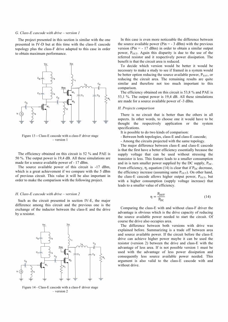
G. Class-E cascode with drive – version 1
The project presented in this section is similar with the one presented in IV-D but at this time with the class-E cascode topology plus the class-F drive adapted to this case in order to obtain maximum performance.
The efficiency obtained on this circuit is 52 % and PAE is 50 %. The output power is 19,4 dB. All these simulations are made for a source available power of - 17 dBm.
The source available power of this circuit is -17 dBm, which is a great achievement if we compare with the 5 dBm of previous circuit. This value it will be also important in order to make the comparison with the following project.
H. Class-E cascode with drive – version 2
Such as the circuit presented in section IV-E, the major difference among this circuit and the previous one is the exchange of the inductor between the class-E and the drive by a resistor.
In this case is even more noticeable the difference between the source available power (Pin = - 3 dBm) with the previous version (Pin = - 17 dBm) in order to obtain a similar output power, POUT. Again this disparity is due to the use of the referred resistor and it respectively power dissipation. The benefit is that the circuit area is reduced.
To decide which version would be better it would be necessary to make a study to see if framed in a system would be better option reducing the source available power, PSAV, or reducing the circuit area. The remaining results are quite similar and therefore not too much important to this comparison.
The efficiency obtained on this circuit is 53,8 % and PAE is 53,1 %. The output power is 19,4 dB. All these simulations are made for a source available power of -3 dBm.
H. Projects comparison
There is no circuit that is better than the others in all aspects. In other words, to choose one it would have to be thought the respectively application or the system specifications.
It is possible to do two kinds of comparison: - Between both topologies, class-E and class-E cascode; - Among the circuits projected with the same topology. The major difference between class-E and class-E cascode
is that the first have a better efficiency essentially because the supply voltage that can be used without stressing the transistor is less. This feature leads to a smaller consumption and in is turn smaller power supplied by the DC supply, PDC. From efficiency, η, equation (14) is clear that if PDC decrease, the efficiency increase (assuming same POUT). On other hand, the class-E cascode allows higher output power, POUT, but with a higher consumption (supply voltage increase) that leads to a smaller value of efficiency.
η =P!"#P!"
(14)
Comparing the class-E with and without class-F driver the
advantage is obvious which is the drive capacity of reducing the source available power needed to start the circuit. Of course the drive also occupies area.
The difference between both versions with drive was explained before. Summarizing is a trade off between area and source available power. If the circuit before the class-E drive can achieve higher power maybe it can be used the resistor (version 2) between the drive and class-E with the advantage of less area. If is not possible version 1 must be used with the advantage of less power dissipation and consequently less source available power needed. This argument is also valid to the class-E cascode with and without drive.
M1
L2
C2
M2
Bias
Vdd
L3
M1
C6
C7
L4
Vi
C5
L5
L0
C1
C4
RL
C3
Vdd
L1
Figure 13 – Class-E cascode with a class-F driver stage – version 1
M1
R1
C2
M2
Bias
Vdd
L3
M1
C6
C7
L4
Vi
C5
L5
L0
C1
C4
RL
C3
Vdd
L1
Figure 14 - Class-E cascode with a class-F driver stage – version 2

V. LAYOUT
When considering the layout design the first thing to do is build a test-bench in Cadence in order to obtain the schematic simulations. In this case the project in test is the one presented in section IV-C, which is the class-E without drive.
The POUT and PAE value obtain through Cadence is similar with the simulations obtain in ADS. The output power, POUT, is 17,94 dBm and the values obtained in ADS is 18,2 dBm. PAE is 54,7 % and the value obtain through ADS is 54,9 %. These values are also for the same source available power (5 dBm) as it was used in ADS.
After schematic simulation the circuit layout was design and is presented in next figure. The main objectives are obtaining slight area and also design connections the smallest possible so that parasites are less representative. Metal 6 was used whenever possible because this metal has the minimum resistance per square.
Figure 15 - Layout
Next figures show the results pos-layout. As it can be seen,
the POUT value doesn’t have a great variation in his value. Remember that in schematic POUT is 17,94 dBm and in pos-layout is 17,72 dBm (figure 16). The same happens with PAE which decrease from 54,69 % in schematic to 51,85 % in pos-layout (figure 17) to the same source available power (5 dBm).
Those variations are perfectly normal in pos-layout and being so the circuit is ready to send to manufacturing.
VI. CONCLUSIONS
Although the better performance of other technologies, the CMOS continues to be fundamental in the field of RF, due to it’s low cost, capability of integration and increasing better performance. Though there aren’t yet scientific contributions really motivating and closer to the foreseen theoretically, the design of this type of circuits in CMOS continues to be important, in order to achieve systems fully integrated in one only chip and with reduced cost.
With this work, it was possible to obtain a global vision of the many ways to do power amplifiers and also to understand the different applications. One of the parameters more important in this type of circuit is with no doubt the capacity to add power, where the class-E as the best performance
Figure 16 - Pout vs Pin
Figure 17 - PAE vs Pin

making it a circuit with a reasonable practical application. Threw this study, a detailed analysis of the class E was obtained that allows to sustain the project of a prototype as well as to perceive some possible configurations and respective advantages and disadvantages.
It was projected the classic class-E topology and also the cascode topology with and without driver stage which is made throw a class-F power amplifier. The simulated results obtained are according to the ones of state-of-the-art and in most cases is overcome.
An output matching network is proposed which allows the using of only capacitors and that correspond also to the capacitive part of the main network tuned filter.
The main objectives are achieved which include the project of a fully integrated class-E power amplifier working at 2,4 GHz and that provides a power output exceeding 17 dBm.
A circuit layout ready for manufacturing is presented..
REFERENCES
[1] G. D. Ewing, “High-Efficiency Radio-frequency Power Amplifier”. PhD thesis, Oregon State University, June 1964.
[2] N. Sokal and A. Sokal, “Class E-a new class of high-efficiency tuned single-ended switching power amplifiers,” IEEE Journal of Solid-State Circuits, vol. 10, pp. 168–76, June 1975.
[3] F. Raab, “Idealized operation of the class E tuned power amplifier,” IEEE Transactions on Circuits and Systems, vol. 24, pp. 725–35, December 1977.
[4] C.-H. Li and Y.-O. Yam, “Maximum frequency and optimum performance of class E power amplifiers,” in IEE Proceedings-Circuits, Devices and Systems, pp. 174–84, 1994.
[5] Bram Nauta, Mustafa Acar, Ane Johan. “Generalized design equations for class-E power amplifiers with finite dc feed inductance”, 36th European Microwave Conference, 2006.
[6] Chengzhou Wang, “CMOS Power Amplifiers for Wireless Communications”. PhD thesis, University of California, San Diego, 2003.
[7] K. L. R. Mertens and M. S. J. Steyaert, “A 700-MHz 1-W Fully Differential CMOS Class-E Power Amplifier”, IEEE Journal of Solid-State Circuit, vol. 37, pp. 137-141, 2002.
[8] K. C. Tsai and P. R. Gray, “A 1.9-GHz, I-W CMOS class-E power amplifier for wireless communications,” IEEE Joumnl of Solid-Slate Circuits, vol. 34, no. 7, pp. 962-970, July 1999.
[9] Chien-Chih Ho, Chin-Wei Kuo, Chao-Chih Hsiao and Yi-Jen. Chan, “A fully integrated class-E CMOS amplifier with a class-F driver stage,” 2003 IEEE MTT-S Radio Frequency Integrated Circuit Symposium Digest, pp. 211-214, 2003
[10] V. Saari, P. Juurakko, J. Ryynanen, K. Halonen, “Integrated 2.4 GHz Class-E CMOS Power Amplifier”, Radio Frequency integrated Circuits (RFIC) Symposium, 2005.
[11] C.C. Ho, C.W. Kuo, C.C. Hsiao and Y.J. Chan, “A fully integrated 2.4 GHz class-E amplifier with a 63% PAE by 0.18 µm CMOS technologies”, Solid State Electronics, vol. 48, pp. 99-102, Jan. 2004.
[12] A. Mazzanti, L. Larcher, R. Brama, and F. Svelto, ‘‘Analysis of Reliability and Power Efficiency in Cascode Class-E PAs,’’ IEEE J. Solid-State Circuits, vol. SC-41, pp. 1222–1229, May 2006.
[13] Leungvongsakorn P, Thanachayanont A. “A 0.1-W CMOS Class-E power amplifier for bluetooth applications”. In: TENCON IEEE conference on convergent technology for Asia-Pacific region, 2003. p. 1348–51.
[14] S. A. Z. Murad, R. K. Pokharel, H. Kanaya, K. Yoshida, O. Nizhnik, “A 2.4-GHz 0,18-um CMOS Class-E single-ended switching power amplifier with a self-biased cascode”, Int. Journal of Electronic and Communications (AEU), (Elsevier publication), 2009.