fully integrated cmos power amplifier
TRANSCRIPT
Fully Integrated CMOS Power Amplifier
Gang Liu
Electrical Engineering and Computer SciencesUniversity of California at Berkeley
Technical Report No. UCB/EECS-2006-162
http://www.eecs.berkeley.edu/Pubs/TechRpts/2006/EECS-2006-162.html
December 6, 2006

Copyright © 2006, by the author(s).All rights reserved.
Permission to make digital or hard copies of all or part of this work forpersonal or classroom use is granted without fee provided that copies arenot made or distributed for profit or commercial advantage and that copiesbear this notice and the full citation on the first page. To copy otherwise, torepublish, to post on servers or to redistribute to lists, requires prior specificpermission.
Fully Integrated CMOS Power Amplifier
by
Gang Liu
B.E. (Tsinghua University) 1998
A dissertation submitted in partial satisfaction of the
requirements for the degree of
Doctor of Philosophy
in
Engineering - Electrical Engineering and Computer Sciences
in the
GRADUATE DIVISION
of the
UNIVERSITY OF CALIFORNIA, BERKELEY
Committee in charge:
Professor Ali M. Niknejad, Co-chair
Professor Tsu-Jae King Liu, Co-chair
Professor Peidong Yang
Fall 2006

The dissertation of Gang Liu is approved:
----------------------------------------------------------------------------------- Co-chair Date
----------------------------------------------------------------------------------- Co-chair Date
----------------------------------------------------------------------------------- Date
UNIVERSITY OF CALIFORNIA, BERKELEY
Fall 2006

Fully Integrated CMOS Power Amplifier
Copyright 2006
by
Gang Liu
1
Abstract
Fully Integrated CMOS Power Amplifier
by
Gang Liu
Doctor of Philosophy in Electrical Engineering and Computer Sciences
University of California, Berkeley
Professor Ali M. Niknejad, Co-chair
Professor Tsu-Jae King Liu, Co-chair
Today’s consumers demand wireless systems that are low-cost, power efficient,
reliable and have a small form-factor. High levels of integration are desired to reduce
cost and achieve compact form factor for high volume applications. Hence the long term
vision or goal for wireless transceivers is to merge as many components as possible, if
not all, to a single die in an inexpensive technology. Therefore, there is a growing
interest in utilizing CMOS technologies for RF power amplifiers (PAs). Although
several advances have been made recently to enable full integration of PAs in CMOS, it
is still among the most difficult challenges in achieving a truly single-chip radio system
in CMOS. This is exacerbated by supply voltage reduction due to CMOS technology
scaling and on-chip passive losses due to the conductive substrate used in deep
submicron CMOS processes.

2
Efficiency is one of the most important metrics in the design of power amplifiers.
Conventional designs give maximum efficiency only at a single power level, usually near
the maximum rated power for the amplifier. As the output power is backed off from that
single point, the efficiency drops rapidly. However, power back-off is inevitable in
today’s wireless communication systems.
To date, there has been relatively little research on the design of a CMOS PA
targeting good average efficiency. A new transformer combining architecture, which is
suitable in designing highly efficient PAs in CMOS processes, is proposed to address this
issue. A prototype was implemented with only thin-oxide transistors in a 0.13-µm RF-
CMOS process to demonstrate the concept. Experimental results validate our concept
and demonstrate the feasibility of highly efficiency, fully integrated power amplifiers in
CMOS technologies.
----------------------------------------------------------
Professor Ali M. Niknejad
Dissertation Committee Co-chair
----------------------------------------------------------
Professor Tsu-Jae King Liu
Dissertation Committee Co-chair

i
Contents Chapter 1: Introduction ....................................................................................................... 1
1.1 Recent developments of wireless communication technologies............................... 1 1.2 Motivation................................................................................................................. 6 1.3 Overview of the work and its contribution ............................................................... 9 1.4 Organization of the thesis ....................................................................................... 11 1.5 References............................................................................................................... 12
Chapter 2: Fundamentals of Power Amplifiers ................................................................ 16
2.1 An overview of classifications and specifications of PAs ...................................... 16 2.1.1 Class-A, AB, B, and C power amplifiers......................................................... 16 2.1.2 Class-D power amplifiers ................................................................................ 18 2.1.3 Class-E power amplifiers................................................................................. 18 2.1.4 Class F power amplifiers ................................................................................. 20 2.1.5 Class-G and Class-H power amplifiers............................................................ 20 2.1.6 Class-S power amplifiers ................................................................................. 21 2.1.7 Hybrid class power amplifiers ......................................................................... 21 2.1.8 Performance metrics of power amplifiers........................................................ 22
2.2 Efficiency of Power Amplifiers .............................................................................. 22 2.3 Linearity of Power Amplifiers ................................................................................ 30
2.3.1 AM-AM Conversion........................................................................................ 31 2.3.2 AM-PM Conversion......................................................................................... 33 2.3.3 Adjacent Channel Power Ratio (ACPR).......................................................... 34 2.3.4 Spectral MASK................................................................................................ 35 2.3.5 Error Vector Magnitude (EVM) ...................................................................... 36 2.3.6 Linearization Techniques................................................................................. 38
2.4 Summary ................................................................................................................. 39 2.5 References............................................................................................................... 39
Chapter 3: CMOS Technology for RF Power Amplifiers ................................................ 42
3.1 Prevalent Technologies for RF Power Amplifiers.................................................. 42 3.1.1 GaAs HBT Technology ................................................................................... 42 3.1.2 GaAs MESFET Technology............................................................................ 44 3.1.3 GaAs HEMT Technology ................................................................................ 45 3.1.4 Si CMOS Technology...................................................................................... 48 3.1.5 SiGe HBT Technology .................................................................................... 51 3.1.6 Si LDMOS Technology ................................................................................... 53
3.2 Comparisons among Prevalent Technologies......................................................... 54 3.2.1 Substrate........................................................................................................... 56

ii
3.2.2 Backside Vias................................................................................................... 57 3.2.3 Passives ............................................................................................................ 58 3.2.3 Device characteristics ...................................................................................... 61 3.2.4 Manufacturing Cost ......................................................................................... 64 3.2.5 Integration ........................................................................................................ 66 3.2.6 Availability & Capacity ................................................................................... 66
3.3 Trends of Supply Voltages for Portable Devices.................................................... 67 3.4. Limits of CMOS and the Impact of Scaling .......................................................... 72
3.4.1 Device Scaling ................................................................................................. 72 3.4.2 Starting Materials............................................................................................. 74 3.4.3 Metal Stack Scaling ......................................................................................... 74
3.5 Summary ................................................................................................................. 75 3.6 References............................................................................................................... 76
Chapter 4: Generating High Power with Low Voltage Devices....................................... 80
4.1 Series Power Combining......................................................................................... 80 4.1.1 Cascode Configuration..................................................................................... 80 4.1.2 Totem-Pole Technique..................................................................................... 83 4.1.3 Stacked Transistors Amplifier ......................................................................... 84
4.2 Parallel Combining ................................................................................................. 85 4.2.1 Transformer Based Power Combining............................................................. 85 4.2.2 Transmission Line Based Power Combining................................................... 88
4.3 Proposed Power Combiner ..................................................................................... 94 4.3.1 Power Combining Transformer ....................................................................... 94
4.4 Summary ............................................................................................................... 114 4.5 References............................................................................................................. 115
Chapter 5. The Power Combining Transformer Design ................................................. 118 5.1 Impedance Transformation ................................................................................... 118
5.1.1 LC Resonant Matching Network ................................................................... 119 5.1.2 Transformer Matching Network .................................................................... 123
5.2 Design Considerations of Transformers for Power Amplifiers ............................ 129 5.2.1 Low Impedance Inductor Design................................................................... 131 5.2.2 Low Turn Ratio Transformer Design ............................................................ 136
5.3 Design and Implementation of the Proposed Transformer ................................... 139 5.4 Discussions and Summary .................................................................................... 143 5.5 References............................................................................................................. 146
Chapter 6. A Fully Integrated CMOS Power Amplifier with Average Efficiency Enhancement................................................................................................................... 148
6.1 Design of the Prototype ........................................................................................ 149 6.1.1 Features of the CMOS Process ...................................................................... 149 6.1.2 PA Architecture ............................................................................................. 149 6.1.3 Power Combining .......................................................................................... 150 6.1.4 Pseudo-Differential Pair................................................................................. 151 6.1.5 Transconductor Design .................................................................................. 152 6.1.6 Cascode Transistor Design ............................................................................ 155

iii
6.1.7 Output Matching Network – Transformer Power Combiner......................... 157 6.1.8 Stability .......................................................................................................... 160
6.2 Layout Considerations .......................................................................................... 162 6.2.1 Transconductor Layout .................................................................................. 162 6.2.2 Cascode Transistor Layout ............................................................................ 165
6.3 The CMOS Prototype ........................................................................................... 166 6.4 Experimental Results ............................................................................................ 170
6.4.1 CW Signal Test .............................................................................................. 171 6.4.2 Modulated Signal Test ................................................................................... 174
6.5 Summary ............................................................................................................... 177 6.6 References............................................................................................................. 177
Chapter 7. Conclusion..................................................................................................... 179
7.1 Thesis Summary.................................................................................................... 179 7.2 Possible Future Directions .................................................................................... 181

1
Chapter 1: Introduction
1.1 Recent developments of wireless communication technologies
1.2 Motivation
1.3 Overview of the work and its contribution
1.4 Organization of the thesis
1.5 References
1.1 Recent developments of wireless communication technologies
Recently the wireless communication industry has seen enormous change. The
fast development of global wireless communications technology has made it the center of
industrial development in the 21st century.
The wave started with cellular phones. Radio phones have a long history that
stretches back to the 1950s, with hand-held cellular devices being available since 1983.
In fact, some of the important fundamentals used in the mobile networks today were
proposed in a patent granted on August 11, 1942 [1.1]. One of the inventors, Hedy
Lamarr1 was actually an actress in Hollywood. She patented an idea (Figure 1.1) about
radio control with the concept of “frequency hopping”, with her friend George Antheil, a
composer.
In the 1980s, cellular phones were first introduced. It was based on cellular
networks with multiple base stations located close to each other, and protocols for the
automated handover between two cells when phones moved from one cell to another. 1 In 1942, at the height of her Hollywood career, Hedy Lamarr patented a frequency-switching system for torpedo guidance that was two decades ahead of its time.
2
Analog transmission was used in every single system, with the support voice
transmissions. These systems later became known as first generation (1G) mobile phones,
such as Advanced Mobile Phone Service (AMPS), Nordic Mobile Telephone (NMT), and
Radio Telefono Mobile Integrato (RTMI). Phones of those days were much larger than
the ones that we use nowadays. They were sometimes better known as “brick phones”
(Figure 1.2 (a)). In the 1990s, second generation (2G) mobile phone systems such as
Global System for Mobile Communication (GSM), Digital AMPS (IS-54 and IS-136
“TDMA”) and IS-95 (CDMA) began to be deployed by service carriers. The availability
of low-cost digital circuits paved the way to adopting advanced digital modulation
schemes. Due to the increased level of usage, service providers started to add more base
stations which led to higher density and smaller size of cellular sites. With other
technological breakthroughs such as more advanced batteries and more power-efficient
electronics, larger “brick phones” were replaced with tiny hand-held devices (Figure 1.3.
(b)). Not long after the introduction of the second generation systems, efforts were
initiated to develop third generation (3G) systems. Before the debut of third generation
systems, 2.5G systems were developed as a stepping stone. 2.5G systems such as
General Packet Radio Service (GPRS), CDMA and Enhanced Data rates for GSM
Evolution (EDGE), can provide some benefits of third generation systems and use some
of the existing second generation network infrastructures. At the beginning of the 21st
century, third generation mobile phone systems such as Universal Mobile
Telecommunication System (UMTS), CDMA 1xEV and Time Division-Synchronous
Code Division Multiple Access (TD-SCDMA) have now begun to be available. High

3
data rates are guaranteed to provide services such as live streaming of video and music
downloading.
Figure 1.1: Two pages of drawings from Lamarr and Antheil's patent. Markey is the
name of Hedy Lamarr's second of six husbands.
In less than twenty years, mobile phones have gone from rare and expensive
pieces of equipment mainly used for business to a pervasive personal item. In many
countries, mobile phones now outnumber land-line telephones, with most adults and

4
many children now owning mobile phones. It is not uncommon for young adults to
simply own a mobile phone instead of a land-line phone for their residence. In some
developing countries, where there is little existing fixed-line infrastructure, the mobile
phone has become widespread. By the end of 2005, the global mobile phone market
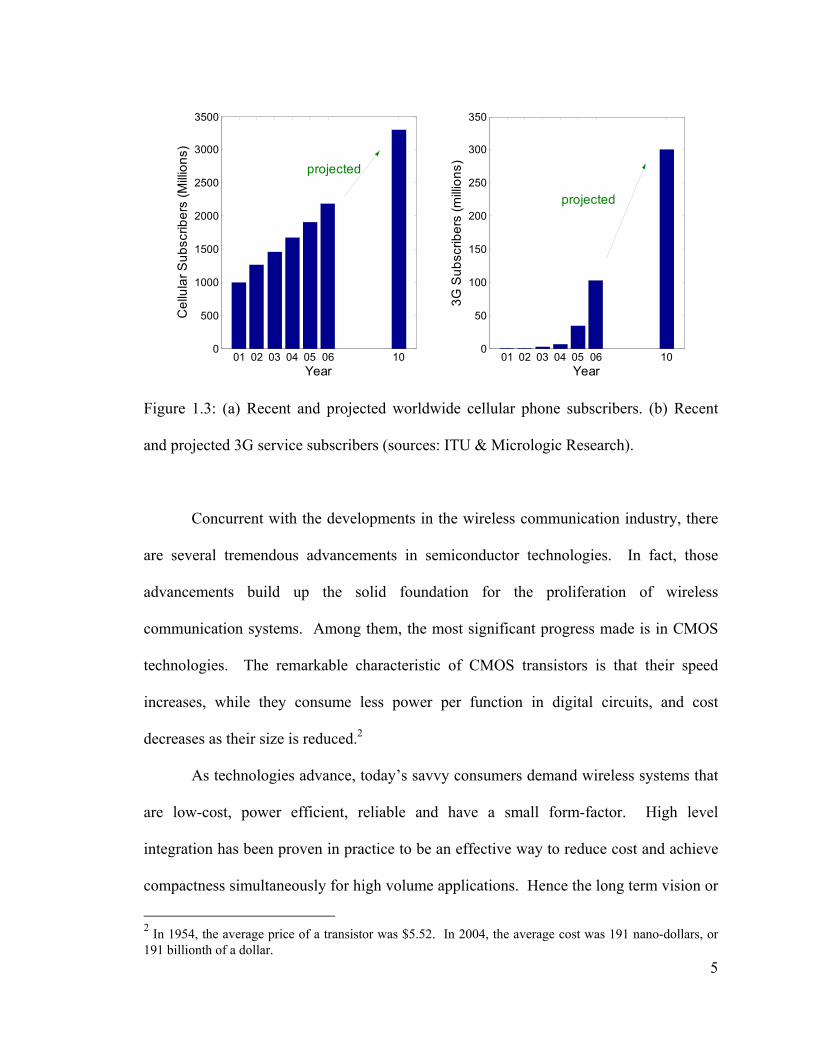
grew to 2 billion subscribers. Yet this market is still growing (Figure 1.3).
(a) (b)
Figure 1.2: (a) Martin Cooper was making a phone call with a Motorola DYNA-TAC
(1973). This phone weighed around 2.5-lb, with 35 minutes talk time. (b) The famous
“Can you hear me now?” guy was talking on a Motorola V325 (2005). This phone
weighs 4.1-oz, with 200 minutes talk time and built-in video camera.
Besides mobile phones, other wireless communication markets are also growing
explosively. Among them, the most well-known systems are probably applications
related to Wireless Local Area Network (WLAN). The WLAN worldwide service
revenues are projected to reach $9.5 Billion by 2007 (source: Alexander Resources). The
looming global rollout of WiMAX will push its way into the 3G market and generate $53
billion in mobile revenue in 2011 (source: TelecomView).
5
01 02 03 04 05 06 100
500
1000
1500
2000
2500
3000
3500
Year
Cel
lula
r Sub
scrib
ers
(Milli
ons)
01 02 03 04 05 06 100
50
100
150
200
250
300
350
Year
3G S
ubsc
riber
s (m
illion
s)projected
projected
Figure 1.3: (a) Recent and projected worldwide cellular phone subscribers. (b) Recent
and projected 3G service subscribers (sources: ITU & Micrologic Research).
Concurrent with the developments in the wireless communication industry, there
are several tremendous advancements in semiconductor technologies. In fact, those
advancements build up the solid foundation for the proliferation of wireless
communication systems. Among them, the most significant progress made is in CMOS
technologies. The remarkable characteristic of CMOS transistors is that their speed
increases, while they consume less power per function in digital circuits, and cost
decreases as their size is reduced.2
As technologies advance, today’s savvy consumers demand wireless systems that
are low-cost, power efficient, reliable and have a small form-factor. High level
integration has been proven in practice to be an effective way to reduce cost and achieve
compactness simultaneously for high volume applications. Hence the long term vision or
2 In 1954, the average price of a transistor was $5.52. In 2004, the average cost was 191 nano-dollars, or 191 billionth of a dollar.

6
goal for wireless transceivers is to merge as many components as possible, if not all, on
to a single die using an inexpensive technology. CMOS was first invented purely for
digital integrated circuits. Gradually CMOS became the predominant technology in
digital integrated circuits since its invention. This trend is essentially because
manufacturing cost, energy efficiency, operating speed and occupied area have benefited
and will continue to benefit from the dimension scaling of CMOS devices that comes
with every new technology generation. All the features mentioned above have allowed
for integration density not possible for other technologies such as silicon bipolar
technology. Besides, radio frequency (RF) and microwave integrated circuits
implemented in CMOS [1.2-1.4] are making a strong appearance in the chip industry. It
is believed that CMOS technology is probably the only viable vehicle at present time to
fulfill the dream of an entire system on a single die at the present time.
1.2 Motivation
Although it was certainly a non-trivial task to realize system-on-chip (SoC),
engineers from industry together with researchers from universities have figured out
ways to put the almost entire system on a single chip [1.5, 1.6]. Yet there is still one
piece missing on the integration chart, the power amplifiers (PAs). Today, almost all
power amplifiers in market are manufactured with III-V compound semiconductors. This
is necessary because high output power and high power efficiency are required power
amplifier specifications in various applications. It is very difficult to satisfy those
requirements with CMOS technologies because of fundamental limitations. On the other
hand, due to the high manufacturing cost associated with those exotic III-V technologies,
7
as well as the incapability of providing complete system solutions, there are growing
interests to look at CMOS technology as an alternative for RF power amplifiers.
Obviously, the ultimate goal is to put the PA, transceiver IC, digital baseband and power
management module on a single piece of silicon.
The first CMOS RF power amplifier that could deliver hundreds mW power was
reported in 1997, implemented in a single-ended configuration with a 0.8-µm CMOS
technology [1.7]. The power amplifier could provide 1-W of output power at
824~849MHz with 62% drain efficiency using 2.5-V supply. The impedance
transformation network was built with off-chip passive components. Single-ended
configuration was the designers’ first choice when power amplifiers were implemented
with discrete transistors. From the integration perspective, it is ill-suited for full
integration since it increases the possibility of coupling with other components on-chip.
The first CMOS RF differential amplifier that could deliver over 1W at GHz range was
reported in 1998, implemented with a 0.35-µm CMOS technology [1.8]. It leveraged
high-Q bond-wires as inductors for the matching network, and micro-strip balun for
differential-to-single-ended conversion at output. Using injection locking technique to
reduce the input drive requirements, the power amplifier could transmit 1-W power at
2GHz with 41% combined power added efficiency using 2-V supply. Since then, there
have been quite a few publications on CMOS RF power amplifiers [1.9-1.13]. They all
rely on off-chip components such as bond-wires, off-chip inductors, off-chip capacitors
to implement low-loss impedance transformation network, and thick-gate-oxide

8
transistors3 to avoid overstressing devices. Since 2G systems were “THE” system at that
time, the majority of published CMOS PAs are nonlinear power amplifiers.
Driven by the demands from customers, continuing efforts have been taken to
look into fully integrated linear CMOS RF power amplifiers. Although there are some
previous publications on fully integrated RF PAs, they were implemented with LDMOS
transistors on a SOI substrate [1.14], or with SiGe HBT transistors in a SiGe BiCMOS
technology [1.15], and other exotic technologies. Without using power combining
techniques, reported fully integrated CMOS power amplifier with 55% drain efficiency
could only achieve 85-mW power at 900-MHz [1.16], or could transmitter 150-mW at -1-
dB compression point at 5-GHz but only with 13% power added efficiency [1.17]. If we
could combine power from several efficient, small power amplifiers, medium-to-high
output power could be achieved with good power efficiency.
Various methods have been used to split and combine RF signals. Among them,
transformers have been widely used as means for combining RF power [1.18]. However,
one serious problem associated with conventional on-chip transformers in CMOS
technologies is high insertion loss which directly translates into loss in power efficiency.
Therefore, this approach has only been adopted to implement inter-stage matching [1.19].
Circular geometry distributive active transformer, known as DAT, was proposed to
overcome high insertion loss problem in on-chip transformers [1.20]. It functions as an
eight-way power combiner with good efficiency at peak output power, implemented with
0.35 µm CMOS transistors [1.21]. Despite many advantages of this approach, the circuit
geometry DAT still has some problems inherently from its structure [1.22, 1.23].
3 Thick oxide devices are devices with recommended supply voltage of 3.3-V or 2.5-V.

9
Besides integration, there is another serious issue associated with PA design
which is inherent to conventional PA. It is well known that a PA can only achieve
maximum efficiency at peak output power. As output power decreases, efficiency drops
rapidly. However, the need to conserve battery power and to mitigate interference to
other users necessitates the transmission of power levels well below the peak output
power of the transmitter [1.24]. Moreover, since spectrum is a scarce commodity,
modern transmitters for wireless communications employ spectrally efficient digital
modulations with time varying envelope. Because of these reasons, the PA transmits
much lower than peak output power under typical operating conditions.
1.3 Overview of the work and its contribution
To date, there has been relatively little research on the design of a CMOS PA
targeting good average efficiency. This work proposes a power combining transformer to
address this issue. This transformer provides measures for simple yet elegant power
control and average efficiency enhancement by modulating the RF load. The control
could be implemented using digital approaches or analog approaches. Average efficiency
enhancement with digital control was successfully demonstrated with a fully integrated
CMOS PA [1.25].
A prototype was fabricated with only thin-gate-oxide transistors in a 0.13-µm
CMOS technology to demonstrate the concept. With 1.2-V supply, it transmits linear
power up to 24-dBm (250-mW) with 25% drain efficiency. When driven into saturation,
it transmits 27-dBm (500-mW) peak power with 32% drain efficiency. As one of the
four amplifiers is turned off for 2.5-dB power back-off from 27-dBm, drain efficiency is
10
improved from 26.5% to 31.5%, very close to instantaneous drain efficiency at peak
power.
To the author’s knowledge, this is the first reported fully integrated CMOS power
amplifier with only thin-gate-oxide transistors in a state-of-the-art CMOS process. It is
capable of transmitting hundreds of mW power. The instantaneous efficiency at peak
output power is good, and can be further improved. The simple and elegant average
efficiency enhancement technique was successfully demonstrated. The significance of
this work is in the following:
1. It proves that fully integrated CMOS power amplifier is feasible and will
continue to be feasible as scaling continues.
2. A power combining technique is proposed based on transformers. Load
modulation can be implemented with digital switches or through
outphasing combining. Extra circuitry overhead is minimum, especially
for the digital approach with switches. The ability of active load pull
greatly enhances the efficiency at power back-off. Other advantages,
such as noise reduction or linearity improvement, could also be obtained,
benefiting from parallelism.
3. It demonstrates that linearity required by advanced modulation schemes
can be achieved with deeply scaled CMOS technologies. As digital
signal processing power increases with the scaling of CMOS, it is the
author’s belief that it will further improve system linearity with little
power overhead and cost penalty.

11
4. Quite rare in power amplifier design, the measurements and simulation
results match pretty well. Therefore, the design methodology used in this
work has been proven to be effective4.
1.4 Organization of the thesis
Chapter 2 presents an overview of power amplifiers, introducing
transconductance power amplifiers, switching power amplifiers, and metrics to evaluate
power amplifiers’ performance. Chapter 3 overviews some prevalent technologies for RF
power amplifier, compare characteristics of CMOS technologies with other technologies.
The trend in supply voltage as technologies advance is touched upon. At the end,
fundamental limitation of CMOS technologies and the impact of scaling for RF power
amplifiers are studied. Chapter 4 presents various existing techniques to generate high
output power with low voltage devices. Then the proposed power combining transformer
will be introduced. Its advantages and potential applications are examined in detail. In
Chapter 5, the design of impedance matching network, especially transformer, is
analyzed. It will give readers a clear picture of what issues should be addressed when
designing on-chip power combining transformer. Chapter 6 presents a detailed
description of design process of the prototype that proves the concept of the power
control and average efficiency enhancement technique. Experimental results are shown
with comparison to simulation results. At last, chapter 7 concludes this work and gives
some suggestion for future research.
4 The author is very indebted to the excellent device models provided by the foundry.

12
1.5 References
[1.1] American Heritage of Invention & Technology, vol. 12, no. 4, Spring 1997
[1.2] B. Razavi, “A 60-GHz CMOS receiver front-end”, IEEE J. Solid-State Circuits, vol.
41, no. 1, pp.17-22, January, 2006
[1.3] C.H. Doan, S. Emami, A.M. Niknejad, R.W. Brodersen, “Millimeter-wave CMOS
design”, IEEE J. Solid-State Circuits, vol. 40, no. 1, pp. 144-155, January 2005
[1.4] A.A. Abidi, “ RF CMOS comes of age”, IEEE J. Solid-State Circuits, vol. 39, no. 4,
pp. 549-561, 2004
[1.5] W. McFarland, W-J. Choi, A. Tehrani, J. Gilbert, J. Kuskin, J. Cho, J. Smith, P. Dua,
D. Breslin, S. Ng, X. Zhang, Y-H. Wang, J. Thomson, M. Unnikrishnan, M. Mack, S.
Mendis, R. Subramanian, P. Husted, P. Hanley, N. Zhang, “A WLAN SoC for video
applications including beamforming and maximum ratio combining”, ISSCC Dig. of
Papers, 2005
[1.6] R.B. Staszewski, R. Staszewski, J.L. Wallberg, T. Jung, C.-M. Hung, J. Koh, D.
Leipold, K. Maggio, P.T. Balsara, “SoC with an integrated DSP and a 2.4-GHz RF
transmitter”, IEEE Trans. on VLSI Systems, vol. 13, no. 11, pp. 1253-1265, November,
2005
[1.7] D. Su, W. McFarland, “A 2.5-V, 1-W monolithic CMOS RF power amplifier”,
IEEE Custom Integrated Circ. Conf. Digest, pp. 189-192, May, 1997
[1.8] K-C. Tsai, P. Gray, “A 1.9GHz, 1-W CMOS class-E power amplifier for wireless
communications”, IEEE J. Solid-State Circuits, vol. 34, no. 7, pp. 962-970, July 1999.
13
[1.9] C. Yoo, Q. Huang, “A common-gate switched, 0.9 W class-E power amplifier with
41% PAE in 0.25µm CMOS”, Symp. on VLSI Circuits, Dig. of Tech. Papers, pp. 56-57,
June, 2000
[1.10] P. Asbeck, C. Fallesen, “A 29 dBm 1.9 GHz class B power amplifier in a digital
CMOS process”, Proc. of ICECS, vol.1, pp. 17-20, 2000
[1.11] T.C. Kuo, B. Lusignan, “ A 1.5 W class-F RF power amplifier in 0.2 µm CMOS
technology”, ISSCC Dig. of Tech. Papers, pp. 154-155, 2001
[1.12] A. Shirvani, D.K. Su, B. Wooley, “A CMOS RF power amplifier with parallel
amplification for efficient power control”, ISSCC Dig. of Tech. Papers, pp. 156-157,
2001
[1.13] C. Fallesen, P. Asbeck, “ A 1 W 0.35 µm CMOS power amplifier for GSM-1800
with 45% PAE”, ISSCC Dig. of Tech. Papers, pp. 158-159, 2001
[1.14] M. Kumar, Y. Tan, J. Sin, L. Shi, J. Lau, “A 900 MHz SOI fully-integrated RF
power amplifier for wireless transceivers”, ISSCC Dig. of Tech. Papers, pp. 382-383,
2000
[1.15] I. Rippke, J. Duster, K. Kornegay, “A fully integrated, single-chip handset power
amplifier in SiGe BiCMOS for W-CDMA applications”, RFIC Symposium, pp. 667-670,
2003
[1.16] R. Gupta, B.M. Ballweber, D.J. Allstot, “Design and optimization of CMOS RF
power amplifiers”, IEEE J. Solid-State Circuits, vol. 36, no. 2, pp. 166-175, February,
2001
14
[1.17] Y. Eo, K. Lee “A fully integrated 24-dBm CMOS power amplifier for 802.11a
WLAN applications”, IEEE Micro. and Wireless Comp. Letters, vol. 14, no. 11, pp. 504-
506, November, 2004
[1.18] H. L. Kraus, C.W. Bostian, and F.H. Raab, “Solid State Radio Engineering”, John
Wiley & Sons, New York, 1980
[1.19] W. Simburger, H. –D. Wohlmuth, P. Weger and A. Heinz, “A monolithic
transformer coupled 5-W silicon power amplifier with 59% PAE at 0.9 GHz”, IEEE J.
Solid-State Circuits, vol. 34, no. 12, pp. 1881-1892, December, 1999.
[1.20] I. Aoki, S. D. Kee, D. Rutledge, and A. Hajimiri, “Distributed active transformer:
A new power combining and impedance transformation technique,” IEEE Trans.
Microwave Theory Tech., vol. 50, no. 1, January, 2002
[1.21] I. Aoki, S. Kee, D. B. Rutledge and A. Hajimiri, “Fully integrated CMOS power
amplifier design using the Distributive Active-Transformer architecture”, IEEE J. Solid-
State Circuits, vol. 37, no. 3, pp. 371-383, March, 2002.
[1.22] S. Kim, K. Lee, J. Lee, B. Kim, S.D. Kee, I.Aoki, D.B. Rutledge, “An optimized
design of distributed active transformer”, IEEE Trans. Microwave Theory Tech., vol. 53,
no. 1, pp. 380-388, January, 2005
[1.23] T.S.D. Cheung, J.R.Long, Y.V. Tretiakov, D.L. Harame, “A 21-27GHz self-
shielded 4-way power-combining PA balun”, Proc. of Custom Integrated Circuits
Conference, pp.617-620, 2004
[1.24] F.H. Raab, P. Asbeck, S. Cripps, P.B. Kenington, Z.B. Popovic, N. Pothecary, J.F.
Sevic, and N.O. Sokal, “Power Amplifiers and Transmitters for RF and Microwave”,
IEEE Transactions on MTT, vol. 50, no.3, pp. 814-826, March 2002.

15
[1.25] G. Liu, T.-J. King Liu, A.M. Niknejad, “A 1.2V, 2.4GHz Fully Integrated Linear
CMOS Power Amplifier with Efficiency Enhancement”, Proc. of Custom Integrated
Circuits Conference, September 2006

16
Chapter 2: Fundamentals of Power Amplifiers
2.1 An overview of classifications and specifications of PAs
2.2 Efficiency of PAs
2.3 Linearity of PAs
2.4 Summary
2.5 References
2.1 An overview of classifications and specifications of PAs
The real world is “analog” in nature. PAs are used, ideally, to amplify signals
without compromising signal integrity, so that information could be transmitted into the
media and recovered by the recipient. PAs may be categorized in several ways,
depending on different criteria. Usually they are classified according to their circuit
configuration and operation conditions into different classes, from class A to Class S.
Since most of the subjects in this section have been covered comprehensively in many
textbooks, what is presented in this section is just a very brief overview. Interested
readers are encouraged consult other literature, such as [2.1-2.3], to probe further.
2.1.1 Class-A, AB, B, and C power amplifiers
These four types of power amplifiers have similar circuit configuration,
distinguished primarily by biasing conditions (Figure 2.1). A class-A power amplifier, in
principle, works as a small-signal amplifier. It is probably the only “true” linear
amplifier, since it amplifies over the entire input cycle such that the output is an exact

17
scaled-up replica of the input without clipping. This “true” linearity is obtained at the
expense of wasting power. To improve efficiency without sacrificing too much linearity,
the concept of “reduced conduction angle” was proposed. The idea is to bias the active
devices5 with low quiescent current and let the input RF signal to turn on active devices
for part of the cycle. As the conduction angle shrinks, the amplifier is biased from class-
AB, to class-B and eventually class-C. Regardless of conduction angle, active devices
are used as current sources. Therefore, they are often referred to as “transconductance”
PAs.
Figure 2.1: A generic topology for class-A, AB, B, and C power amplifiers
Using a class-A power amplifier with 1.2-V supply voltage as an example, ideal
maximum output power delivered to the 50-Ω antenna is calculated as:
mWR
VP
L
ddout 4.14
5022.1
2
22
=⋅
=⋅
=
5 Power amplifiers can be either designed in single-ended or pseudo-differential topology. pl. are used to describe amplifiers in text, though illustrations are shown in single-ended topology.

18
Obviously this output power is not high enough for most of the applications today.
Therefore impedance transformation is necessary. For example, in order to transmit 300-
mW power, the 50-Ω load should be transformed to:
Ω=⋅
=⋅
= 4.23.02
2.12
22
out
ddL P
VR
In real practice, due to various losses, RL need to be even lower for the same output
power which poses a serious challenge. This issue will be revisited.
2.1.2 Class-D power amplifiers6
A class D amplifier is composed of a voltage controlled switch and a filtering tank.
Figure 2.2 shows a voltage switching class D amplifier. The output tuned network is
tuned to the fundamental frequency. It will thus have negligible impedance at
fundamental frequency and high impedance at harmonic frequencies. The analysis of
such an amplifier is very straightforward due to the simple drain voltage waveform. In an
ideal situation, the drain efficiency of a class-D amplifier reaches 100% as other
switching type PAs.
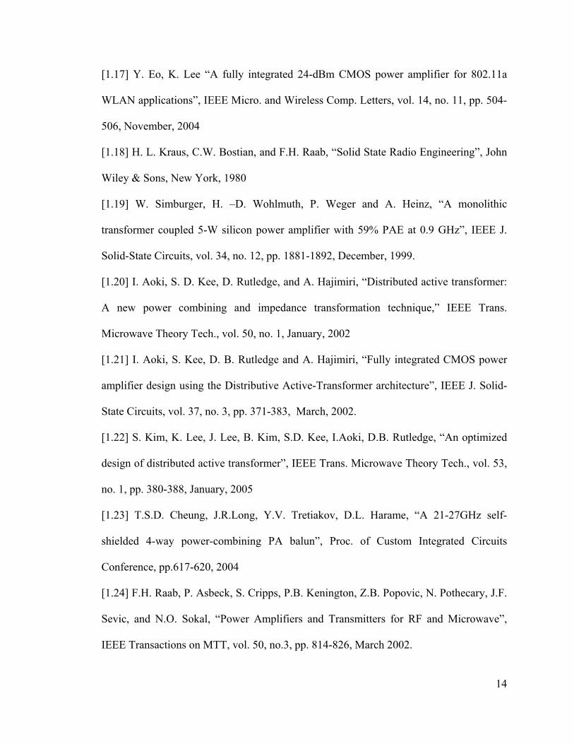
2.1.3 Class-E power amplifiers
Class-E PA stands out from other highly efficient switching PAs because parasitic
capacitances of active devices may be absorbed into wave-shaping/matching networks.
A simplest form of class-E PAs is shown in Figure 2.3. During operation, the waveforms
6 The letter D does not stand for “digital”, even though active devices are operated as switches. The letter D is used to designate this type of amplifier simply because “D” is the next letter after “C”.
19
of drain current and voltage are shaped such that they do not overlap. Furthermore, the
voltage will decrease gradually to zero before the active device turns on. This avoids
charging/discharging capacitors at the drain, thus improve efficiency. However, the
class-E PA has its disadvantage in terms of peak voltage.
Figure 2.2: A voltage switching class-D amplifier
Figure 2.3: A simple class-E amplifier
20
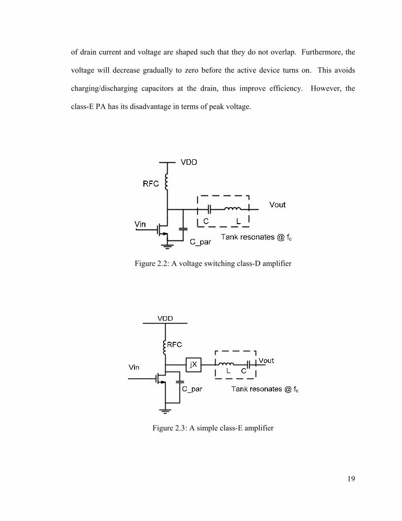
2.1.4 Class F power amplifiers
Class-F is characterized by a load network that has resonance at one or more
harmonic frequencies as well as at the fundamental frequency (Figure 2.4). To the
author’s knowledge, class-F was first proposed to improve the efficiency of overdriven
transconductance amplifiers. Therefore, the active devices typically operate as a
transconductor (or a current source) as those in transconductance amplifiers. However, if
the input drive is large, active devices will behave as switches just like those in switching
amplifiers. In practice with lumped elements, it is rare to see class-F amplifiers with
tuned harmonics higher than the 5th harmonic, due to the complexity of a waveform
shaping network.
Figure 2.4: A class-F power amplifier with tuned harmonics for waveform shaping
2.1.5 Class-G and Class-H power amplifiers
Class-G amplifier is just a more efficient version of transconductance power
amplifiers. This type of amplifier switches supply rails when necessary. This results in
an overall improvement in efficiency for signals which do not continuously require the

21
higher voltage supply. Class-H amplifiers are similar to class-G, which takes the class-G
design one step further. Instead of discretely switching supply rails, the power supply is
modulated by the input signal, to provide just enough voltage for optimum efficiency.
Sometime, it is referred as “kahn” technique or “envelope following” technique.
2.1.6 Class-S power amplifiers
Class-S PAs looks like Class-D PAs, with one difference. The input to a Class-D
PA has 50% duty cycle. Thus a standalone class-D PA cannot be used for modulation
schemes with amplitude modulation. Class-S, however, may be used for amplitude
modulation with excellent efficiency. The basic principle involves the creation of a
rectangular waveform of variable duty-cycle, such that different pulse widths (duty cycles)
produce different average outputs to form the desired waveform7.
2.1.7 Hybrid class power amplifiers
The classes of power amplifiers have their advantages and disadvantages
respectively. To overcome some limitations and further improve amplifier performance,
several hybrid classes were proposed. Among them, a class-BD power amplifier [2.4]
and a class-E/F family of power amplifiers [2.5] are of particular interest. The Class-BD
power amplifier has a linear transfer characteristic, and efficiency higher than that of a
class-B power amplifier with the same peak output power. The class-E/F family of
amplifiers has class-E features such as incorporation of the transistor parasitic
7 The working principle of class S is somewhat similar to sigma-delta modulator.

22
capacitance into the circuit. Additionally, some number of harmonics may be shaped in
the fashion of inverse class-F in order to achieve desirable voltage and current waveforms
for improved performance.
2.1.8 Performance metrics of power amplifiers
There are many metrics used to evaluate the performance of power amplifiers.
Some of the metrics are specified by regulations or standards. Other metrics are not
specified, though they are often used for comparing different power amplifiers for the
same application. Depending on the type of applications, gain, output power, ruggedness,
linearity, efficiency, size and/or noise could be the metrics that differentiate different
amplifiers. Among them, efficiency and linearity are probably the most commonly used
metrics. Those two metrics are correlated in the design process, and present two inherent
problems to power amplification of amplitude modulated RF signals. In the following
setions of this chapter, those two metrics will be studied in detail.
2.2 Efficiency of Power Amplifiers
One of the most important metrics for a power amplifier is its power efficiency.
It is a measure of how well a device converts one energy source to another. What does
not get converted is dissipated into heat which is almost universally a bad product of
energy conversion. In RF circuit design, power amplifier efficiency is calculated in three

23
ways with wide acceptance. The first one is drain efficiency8, usually denoted as ηD.
This is defined as the ratio of output power POUT to DC power consumed from supply
PSUPPLY:
SUPPLY
OUTD P
P=η
Drain efficiency does not take input power into account. If the gain is high, it is safe to
ignore the effect of input power. However, in RF power amplifiers, the input power can
sometime be substantial, therefore measures that include the effect of input power are
necessary. Power added efficiency (PAE), denoted as ηPAE, is the most common used
measure which takes input power into account. It is calculated as the ratio of the
difference between output power POUT and input power PIN to DC power consumed from
supply PSUPPLY:
SUPPLY
INOUTPAE P
PP −=η
If the gain of the amplifier is known, PAE can be expressed in terms of the gain G and
drain efficiency ηD:
)11()11(
GPG
P
PPP
DSUPPLY
OUT
SUPPLY
INOUTPAE −⋅=
−=
−= ηη
If the gain is high, PAE approaches drain efficiency. In a chain of cascaded amplifiers, if
each amplifier has the same PAE, then the PAE of the entire chain will be exactly the
same as the PAE of an individual amplifier. A less frequently used measure is called
8 Drain efficiency gets its name from FET devices, though it probably should be called collector efficiency when BJT devices are used.

24
total efficiency, denoted as ηTOTAL. It is calculated as the ratio of output power POUT to
the sum of input power PIN and DC power consumed from supply PSUPPLY:
SUPPLYIN
OUTTOTAL PP
P+
=η
In fact, total efficiency is the measure that makes the most sense from a thermodynamic
point of view. This can be seen by noting that the total dissipated power is simply a
function of the output power POUT and total efficiency ηTOTAL. This measure can be used
to evaluate the effectiveness of an amplifier and estimate heat removal requirements.
Nonetheless, PAE is still the most popular measure in industry. One point that should be
noted here is that all three measures mentioned above are for instantaneous efficiency.
Conventional power amplifier designs give maximum efficiency only at a single
power level, usually near the maximum rated power for the amplifier. As the output
power is backed off from that single point, the efficiency typically drops rapidly.
However, back-off situation is inevitable in today’s wireless communication. First, the
need to conserve battery power and to mitigate interference to other users necessitates the
transmission of power levels well below the peak output power. Transmitters will only
use peak output power when necessary. Second, the requirement for both high data rate
and efficient utilization of the increasingly crowded spectrum necessitates the use of both
amplitude and phase modulation schemes. In a number of applications, it is more
convenient and robust to use a large number of carriers with low data rates than a single
carrier with a high data rate. For example, orthogonal frequency division multiplexing
(OFDM) employs multiple carriers with the same amplitude modulation, separated in
frequency and codes so that the modulation products from one carrier are zero at the
25
other carriers in an ideal system. The resultant composite signal has a peak-to-average
ratio in the range of 12~17-dB.
Obviously, high instantaneous efficiency at peak output level is certainly
desirable. However, what more important is the average efficiency. Or in other words,
power amplifiers need to maintain high efficiency over a wide dynamic range. Therefore,
average efficiency is a useful measure. Average drain efficiency, denoted as η , is
calculated as the ratio of average output power OUTPUTP to the average DC power from
supply SUPPLYP , depending on both the instantaneous efficiency of the power amplifier η
and the probability-density function (PDF) of the signal it’s amplifying:
SUPPLY
OUTPUT
PP
=η
If the PDF of the output power is p(POUTPUT) is known, average output power is
expressed as:
∫ ⋅⋅=MAXOUTP
OUTPUTOUTPUTOUTPUTOUTPUT dPPpPP_
0
)(
And average DC power from the supply is expressed as:
∫ ⋅⋅=MAXOUTP
OUTPUTOUTPUTSUPPLYSUPPLY dPPpPP_
0
)(
Therefore, average efficiency η can be expressed in terms of instantaneous efficiency η
and PDF of the output power p(POUTPUT):
∫ ⋅⋅=MAXOUTP
OUTPUTOUTPUT dPPp_
0
)(ηη

26
As an example, average drain efficiency of an ideal class-A amplifier is studied.
An ideal class-A amplifier has 50% drain efficiency at peak output power, ηD_peakpower. If
the input signal consists of two sinusoidal tones of equal amplitude, the average drain
efficiency is 25%, half of the drain efficiency at peak output power. This can be
generalized for a multi-tone signal consisting of N sinusoidal tones of equal amplitudes,
the average efficiency is:
peakpowerDN _1 ηη ⋅=
If N is 52, then average drain efficiency is less than 1%. Now let’s look at somewhat
more realistic OFDM signals with N sub-carriers. It is fair to assume that the signal
power is uniformly distributed over the N sub-carriers using the same QAM constellation
for each one of them. For a large value of N (>30), the CDF of OFDM symbols can be
well approximated by that of a two-dimensional complex Gaussian random process,
according to the Central Limit Theorem. Consequently, the envelope of such an OFDM
signal can be considered as Rayleigh distributed. The PDF of this OFDM signal is shown
in Figure 2.5. For comparison, the PDF of a constant amplitude signal is also shown in
Figure 2.5. While the average drain efficiency of an ideal class A amplifier for the
constant amplitude signal is 50%, the average drain efficiency of such an amplifier for
the OFDM signals is only 5%. For most other classes of amplifiers, similar but different
level of degradation in average efficiency is inevitable when amplifying signals with
amplitude modulation.
This is only part of the problem. In real life, transmitters seldom transmit full
output power. The PDF of a single carrier mobile transmitter is shown in Figure 2.6 [2.6].
The PDF of the transmitted power depends on various factors, such as the distance to the
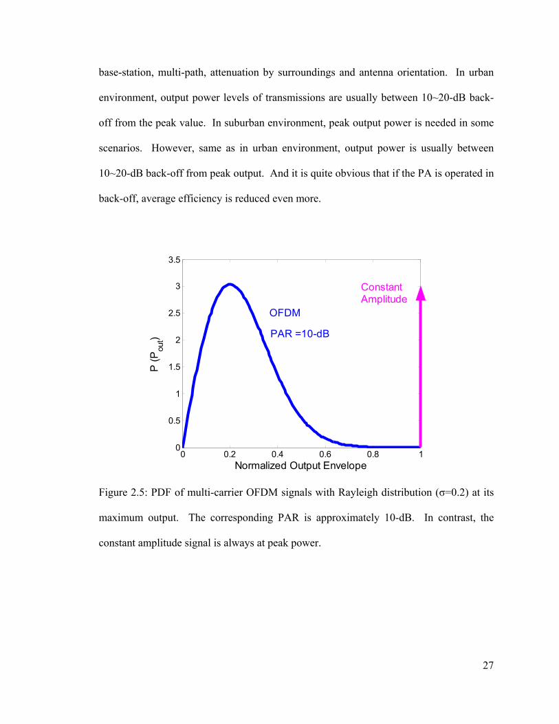
27
base-station, multi-path, attenuation by surroundings and antenna orientation. In urban
environment, output power levels of transmissions are usually between 10~20-dB back-
off from the peak value. In suburban environment, peak output power is needed in some
scenarios. However, same as in urban environment, output power is usually between
10~20-dB back-off from peak output. And it is quite obvious that if the PA is operated in
back-off, average efficiency is reduced even more.
0 0.2 0.4 0.6 0.8 10
0.5
1
1.5
2
2.5
3
3.5
Normalized Output Envelope
P (P
out) PAR =10-dB
OFDM
ConstantAmplitude
Figure 2.5: PDF of multi-carrier OFDM signals with Rayleigh distribution (σ=0.2) at its
maximum output. The corresponding PAR is approximately 10-dB. In contrast, the
constant amplitude signal is always at peak power.

28
-60 -40 -20 0 20 400
0.01
0.02
0.03
Pout (dBm)
P (P
out)
suburbanurban
Figure 2.6: Output Power PDF of a single carrier mobile transmitter
Several efficiency enhancement techniques have been proposed to overcome this
issue9. A brief review will be given here. To begin with, let’s study the drain efficiency
of a class-A amplifier first:
DCSUPPLY
OUTPUT
SUPPLY
OUTPUTD IV
PPP
⋅⋅==
21η
Class-A is used as an example here for simplicity. Similar relationships exist for other
classes of power amplifiers. From this simple equation, several ways can be pointed out
to increase average efficiency. The basic idea is to design an adaptive power amplifier so
that it can self-adjust to optimize efficiency based on the output power requirement:
a. Dynamic bias: the idea of improving efficiency by changing the amplifier
quiescent current is very straightforward. In class-AB mode, the dc average 9 Some techniques were proposed in the early days of radio broadcasting. The motivation was to solve the thermal management issue and to lower cost. In wireless communication, the motivation is to extend the battery time in between charging of portable devices.

29
current varies automatically with output power level. In class-B mode, the dc
average current varies according to the square root of output power. As a result,
drain efficiency varies proportionally to the square root of output power
(POUTPUT0.5) in class-B mode, while it varies proportionally to POUTPUT in class-A
mode. Hence, changing bias conditions as a function of input power can also be
used. The limit of this method is set by the tradeoff between tolerance of gain
variation and linearity [2.7].
b. Dynamic supply: drain efficiency, ηD, is a strong function of the supply voltage.
It is also possible to vary the dc supply voltage in accordance with the output
power level 10 . Switching regulators are probably most suitable for battery-
dependent applications because of their high efficiency compared to linear
regulators. Furthermore, switching regulators are capable of producing output
voltages that are both lower and higher than their input voltages.
Implementations have been published many times recently. However, they are
limited to narrow band applications [2.8, 2.9]. In addition, noise and inter-
modulation products from the switching supply need further careful investigation.
c. Dynamic load: A different approach can be taken to increase the efficiency at
power back-off. This can be seen in the equation below:
DCSUPPLY
LOUTPUT
SUPPLY
OUTPUTD IV
RVPP
⋅⋅==
/21 2
η
For a given output power, VOUTPUT will increase proportionally to the square root
of the load impedance. Therefore, load switching can also be employed to
enhance the low power efficiency. Doherty amplifier [2.10] and Chireix’s [2.11]
10 Recall Class G, Class H, Class S power amplifiers

30
amplifier are examples of this technique. Dynamic switched load technique has
also been demonstrated [2.12].
For transconductance power amplifiers, the most desirable solution is to vary two
variables simultaneously, such as DC current and supply voltage, or DC current and load.
2.3 Linearity of Power Amplifiers
Besides efficiency, another inherent problem of power amplifiers is linearity. All
radio systems are required to induce the minimum possible interference to other users.
Hence, they must keep their transmissions within the bandwidth allocated and maintain
negligible energy leakage outside of the band. If signals are distorted due to
nonlinearities, unwanted distortion products present to other users as interference.
Furthermore, good linearity is mandated in order to preserve the integrity of the
information in transmitted signals. Therefore, modulated signals could be recovered at
the receive end.
A fully rigorous distortion analysis of a power amplifier is lengthy and highly
mathematical. Instead, a traditional approach to analyze distortions with power series is
adopted here11. The transfer characteristic of a differential power amplifier is expressed
as12:
...)()()()( 55
331 +++= tsatsatsats iiio
11 Full treatment could be found in [2.13] 12 In wide-band wireless communications, even order distortions are also falling in-band. Differential topology will greatly suppress distortion products from even order terms.

31
2.3.1 AM-AM Conversion
AM-AM conversion is a phenomenon of the nonlinear relationship between
amplitude of input and output in all practical power amplifiers. The most commonly
used metric for this one is probably -1dB compression point (P-1dB). A single sinusoidal
input signal is applied to the circuit:
tstsi ωcos)( =
So the output is:
...)(cos)cos()( 133
311 ++= tsatsatso ωω
Consider the fundamental terms:
)cos(...)43( 1
331 tsasa ω++
Ignore higher order (>3) terms, the gain becomes:
)431( 2
1
31 s
aa
aG +=
If the coefficient a1 and a3 have opposite signs, the gain will compress when the input
increases. At some point, the gain will be 1-dB lower than the small-signal gain:
11.034
3
1,1 ⋅=− a
aP inputdB
Another way to look at AM-AM conversion is to look at inter-modulation (IM) products,
because IM products will overlay with wanted-signal band in modulated signals. If the
input consists of two in-band RF signals with equal amplitude, whose spacing is much
smaller than carrier frequency:
)cos()cos()( 21 tststsi ωω +=
32
the output becomes:
...)]cos()[cos(
)]cos()([cos
)]cos()[cos()(
521
55
321
33
211
+++
++
+=
ttsa
ttsa
ttsatso
ωω
ωω
ωω
Consider the third-order terms:
])2cos()2cos(cos2[43
])2cos()2cos(cos2[43
)cos33(cos4
)cos33(cos4
)]cos()[cos(
212123
3
121213
3
22
33
11
33
321
33
tttsa
tttsa
ttsa
ttsa
ttsa
ωωωωω
ωωωωω
ωω
ωω
ωω
++−++
++−++
++
+=
+
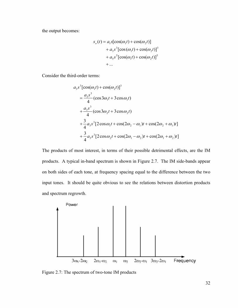
The products of most interest, in terms of their possible detrimental effects, are the IM
products. A typical in-band spectrum is shown in Figure 2.7. The IM side-bands appear
on both sides of each tone, at frequency spacing equal to the difference between the two
input tones. It should be quite obvious to see the relations between distortion products
and spectrum regrowth.
Figure 2.7: The spectrum of two-tone IM products
33
2.3.2 AM-PM Conversion
Comparing to well understood amplitude distortion, phase distortion effects are
less seen in literature. This is probably due to the difficulty in AM-PM measurements,
and the lack of metrics, such as P-1dB for AM-AM conversion. Nonetheless, this becomes
more and more important with modern modulation schemes13. This AM-PM conversion
probably can be traced back to the signal-level dependency of parasitic capacitors in
active devices, especially MOSFETs input gate capacitance [2.14]. It should not be a
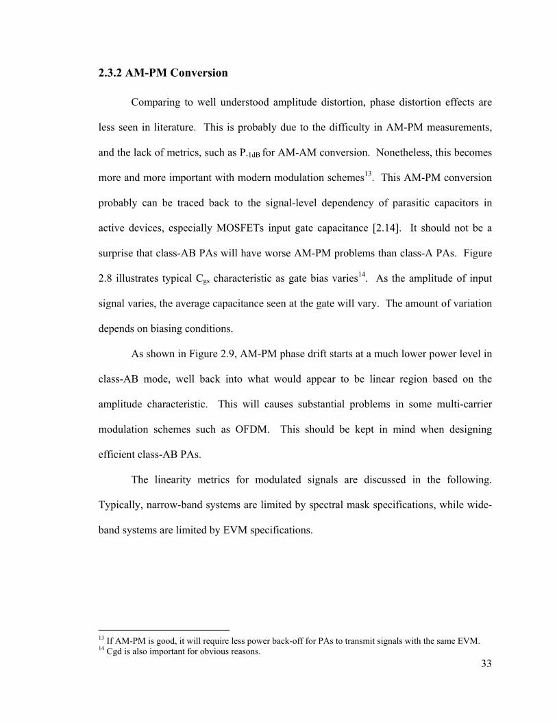
surprise that class-AB PAs will have worse AM-PM problems than class-A PAs. Figure
2.8 illustrates typical Cgs characteristic as gate bias varies14. As the amplitude of input
signal varies, the average capacitance seen at the gate will vary. The amount of variation
depends on biasing conditions.
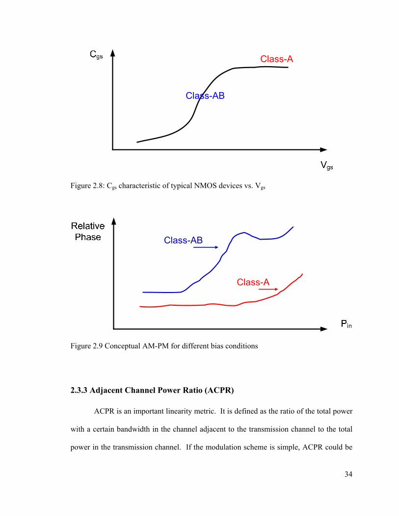
As shown in Figure 2.9, AM-PM phase drift starts at a much lower power level in
class-AB mode, well back into what would appear to be linear region based on the
amplitude characteristic. This will causes substantial problems in some multi-carrier
modulation schemes such as OFDM. This should be kept in mind when designing
efficient class-AB PAs.
The linearity metrics for modulated signals are discussed in the following.
Typically, narrow-band systems are limited by spectral mask specifications, while wide-
band systems are limited by EVM specifications.
13 If AM-PM is good, it will require less power back-off for PAs to transmit signals with the same EVM. 14 Cgd is also important for obvious reasons.
34
Class-AB
Class-A
Figure 2.8: Cgs characteristic of typical NMOS devices vs. Vgs
Class-AB
Class-A
Figure 2.9 Conceptual AM-PM for different bias conditions
2.3.3 Adjacent Channel Power Ratio (ACPR)
ACPR is an important linearity metric. It is defined as the ratio of the total power
with a certain bandwidth in the channel adjacent to the transmission channel to the total
power in the transmission channel. If the modulation scheme is simple, ACPR could be
35
derived from IM distortion products accurately. However, as the modulation becomes
more complex, sinusoidal representation is no longer adequate to address this problem.
Table 2.1 gives examples of some current definitions of locations of measurement
channels and their bandwidth (BW) for ACPR metric of two CDMA systems. For
CDMA IS-95, ACPR30_30spec is -42-dBc at first frequency offset and -54-dBc at the
second frequency offset.
CDMA IS-95 WCDMA
Main channel measurement BW 1.23-MHz or 30-kHz 3.84-MHz
Adjacent channel location
(from carrier) ± 885-kHz ± 5-MHz
Adjacent channel measurement
BW 30-kHz 3.84-MHz
Alt channel location
(from carrier) ± 1.98-MHz ± 10-MHz
Alt channel measurement BW 30-kHz 3.84-MHz
Table 2.1: Current definitions of locations of measurement channels and their bandwidth
for ACPR of two CDMA systems
2.3.4 Spectral MASK
A similar metric to ACPR is spectral mask. The power spectral density of a
power amplifier is sometimes referred as spectral emission. A spectral mask is generally
36
intended to reduce the interference by limiting excessive radiation at frequencies beyond
the necessary bandwidth. Figure 2.10 shows the spectral mask specified in the
GSM/EDGE standard. The graph illustrates the maximum allowed power density,
normalized to the power density within the signal band, as a function of the frequency
offset from the carrier.
-600 -400 -200 0 200 400 600-80
-70
-60
-50
-40
-30
-20
-10
0
Frequency [kHz]
Pow
er [d
B]
-54dBc
-60dBc
-600 -400 -200 0 200 400 600-80
-70
-60
-50
-40
-30
-20
-10
0
Frequency [kHz]
Pow
er [d
B]
-54dBc
-60dBc
Figure 2.10: GSM-EDGE spectral mask
2.3.5 Error Vector Magnitude (EVM)
The EVM is a measure used to quantify the performance of a system with phase-
shift modulation. Due to various impairments, the actual constellation points will move
relative to the ideal constellation locations. EVM is a measure of how far the actual
constellation points are from the ideal locations (Figure 2.11).
37
(a)
(b)
Figure 2.11: A rectangular 16-QAM constellation diagram: (a) ideal; (b) actual

38
2.3.6 Linearization Techniques
Because of the stringent requirement on linearity and the desire to increase battery
time, several linearization techniques have been developed to enable linear systems with
more efficient, but nonlinear or less linear power amplifiers. As wireless communication
evolve, it seems that a standalone linear power amplifier cannot meet linearity
requirements posed by the next generation wireless systems. Therefore, some degree of
linearization around the amplifier is necessary even if the amplifier itself is “linear”.
Reference [2.15] has quite extensive coverage on this topic. Here some techniques will
be discussed very briefly.
Feedback is probably the most obvious method to reduce distortion of power
amplifiers. The improvement on linearity is dependent on the loop gain which could be
quite expensive to obtain at RF frequencies. And stability is also a concern because time-
delay is not negligible at RF frequencies. Cartesian loop [2.16] and polar loop [2.17] are
two most popular feedback techniques.
To avoid problems with feedback at RF frequencies, feedforward15 techniques
have been proposed for linear power amplifiers. The input signal is split into two paths,
and then combined after amplification, such that wanted signal are in-phase and
distortions cancel out [2.15].
Predistortion is conceivably the simplest linearization technique, since it is open-
loop in nature. Nonlinearities of power amplifiers can be corrected for at the input of the
amplifier by predistortion [2.18]. The predistortion, in theory, will be cancelled out by
distortions of power amplifiers. An overall linear transfer characteristic can thus be
15 Actually, the inventor, H.S. Black, filed patent of feedforward 9 years earlier than the patent of feedback.

39
obtained. This technique was mainly used for base-station because it was power hungry.
With the scaling of CMOS, it becomes practical to implement this technique on portable
devices.
2.4 Summary
A brief overview of different classes of amplifiers was provided. Among many
metrics that evaluate performance of power amplifiers, efficiency and linearity are
particularly emphasized, because they represent fundamental trade off in power amplifier
designs in modern multi-carrier systems. This is even more exacerbated if CMOS
technologies are used as the design platform.
2.5 References
[2.1] Steve C. Cripps, “RF Power Amplifiers for Wireless Communications”, Artech
House, 1999.
[2.2] T.H. Lee, “The design of CMOS radio-frequency integrated circuits”, 1st Edition,
Cambridge University Press, 1998
[2.3] H. L. Kraus, C.W. Bostian, and F.H. Raab, “Solid State Radio Engineering”, New
York Wiley, 1980
[2.4] F.H. Raab, “The class BD high-efficiency RF power amplifier”, IEEE J. Solid-State
Circuits, vol. sc-12, no. 3, pp. 291-298, June 1977

40
[2.5] S.D. Kee, I. Aoki, A. Hajimiri, D.B. Rutledge, “The class-E/F family of ZVS
switching amplifiers”, IEEE Trans. Microwave Theory Tech., vol. 51, no. 6, pp. 1677-
1690, June 2003
[2.6] F.H. Raab, P. Asbeck, S. Cripps, P.B. Kenington, Z.B. Popovic, N. Pothecary, J.F.
Sevic, and N.O. Sokal, “Power Amplifiers and Transmitters for RF and Microwave”,
IEEE Transactions on MTT, vol. 50, no.3, pp. 814-826, March 2002.
[2.7] J. Deng, P.S. GUdem, L.E. Larson, P.M. Asbeck, “A high average-efficiency SiGe
HBT power amplifier for WCDMA handset applications”, IEEE Transactions on MTT,
vol. 53, no. 2, pp. 529-537, February 2005
[2.8] B. Sahu, G.A. Rincon-Mora, “A high-efficiency linear RF power amplifier with a
power-tracking dynamically adaptive buck-boost supply”, IEEE Transactions on MTT,
vol. 52, no. 1, pp. 112-120, January 2004
[2.9] G. Hanington, P-F. Chen, P.M. Asbeck, L.E. Larson, “ High-efficiency power
amplifier using dynamic power-supply voltage for CDMA applications”, IEEE
Transactions on MTT, vol. 47, no. 8, pp. 1471-1476, August 1999
[2.10] W. H. Doherty, “A new high efficiency power amplifier for modulated waves”, in
Proc. IRE, vol. 24, pp. 1163-1182, September 1936
[2.11] H. Chireix, “High power outphasing modulation”, Proc. IRE, vol. 23, no. 11, pp.
1370-1392, November 1935
[2.12] F.H. Raab, “ High-efficiency linear amplification by dynamic load modulation”,
IEEE MTT-S Digest, vol. 3, pp.1717-1720, June 2003
[2.13] R.G. Meyer, EE242 course notes, EECS, UC Berkeley

41
[2.14] C. Wang, M. Vaidyanathan, L.E. Larson, “A capacitance-compensation technique
for improved linearity in CMOS class-AB power amplifiers”, IEEE J. Solid-State
Circuits, vol. 39, no. 11, pp. 1927-1937, November 2004
[2.15] P. B. Kenington, “High linearity RF amplifier design”, Artech House Inc, 2000
[2.16] J. L. Dawson, T.H. Lee, “Automatic phase alignment for a fully integrated
Cartesian feedback power amplifier systems”, IEEE J. Solid-State Circuits, vol. 38, no.
12, pp. 2269-2279, December 2003
[2.17] P. Reynaert, M. Steyaert, “A 1.75-GHz polar modulated CMOS RF power
amplifier for GSM-EDGE”, IEEE J. Solid-State Circuits, vol. 40, no. 12, pp. 2598-2608,
December 2005
[2.18] N. Safari, J.P. Tanem, T. Roste, “A block-based predistortion for high power-
amplifier linearization”, IEEE Transactions on MTT, vol. 54, no. 6, pp. 2813-2820, June
2006

42
Chapter 3: CMOS Technology for RF Power Amplifiers
3.1 Prevalent technologies for RF power amplifiers
3.2 Comparisons among prevalent technologies
3.3 Trends of supply voltages for portable devices
3.4 Limits in CMOS technologies and the impact of scaling
3.5 Summary
3.6 References
3.1 Prevalent Technologies for RF Power Amplifiers
Over the past several decades, various technologies (materials and devices) have
been used to implement power amplifiers in the radio-frequency/millimeter-wave
frequency range. The benefits of each technology vary, as do the drawbacks. Only a few
of those technologies are currently in use. Features of those technologies will be briefly
reviewed in this section.
3.1.1 GaAs HBT Technology
The concept of Heterojunction bipolar transistors is not a new one and was
described by Schockley in a patent [3.1] filed in 1948, though the technology was not
feasible until recent years because of the improvements in epitaxial crystal growth. The
HBT is basically a npn bipolar transistor consisting primarily of three layers of doped
semiconductor to form two junction diodes [3.2], i.e. for a large current gain, electrons
are required to pass from the forward-biased emitter-base junction, through the p-type
43
base region, into the collector depletion region, with a minimum recombination with
holes on the way. In the meantime, reverse hole injection from the base to the emitter
should be minimized. The difference between the HBT and the standard bipolar junction
transistor lies in the materials used to form junctions. Using a wide band-gap emitter in
an npn HBT presents larger barrier experienced by holes than by electrons, which
restricts the flow of minority carriers (holes) from the base into the emitter regardless of
the doping levels on either side of the junctions.
Figure 3.1 illustrates a representative npn GaAs HBT cross-section. A typical
GaAs technology provides npn transistors, thin film transistors, several metal layers
(usually two) for interconnects with plated thick Au (~10-µm) as low-loss top level metal.
MIM capacitors could be available or finger capacitors could be formed using
interconnects. Inductors can be realized by patterning the metal layers. Due to the semi-
insulating substrate used, as well as thick top metal layer, high Q passive elements could
be realized on-chip. The 12.9 dielectric constant and semi-insulating substrate make it an
excellent media for micro-strip and CPW (coplanar wave) design. A GaAs HBT
technology also features through-wafer vias which provide low inductance ground
connections from the top side of the die to the underlying ground plane. HBTs only
require a single supply voltage for normal operation, and have very good high-frequency
power performance.
For the last several years, AlGaAs/InGaP GaAs HBT power amplifiers have
dominated the handset transmitter market due to their excellent power added efficiency
and superior linearity when used in the CDMA systems. However, the substrate of GaAs
wafers is not a good thermal conductor, and has to be thinned for optimum performance
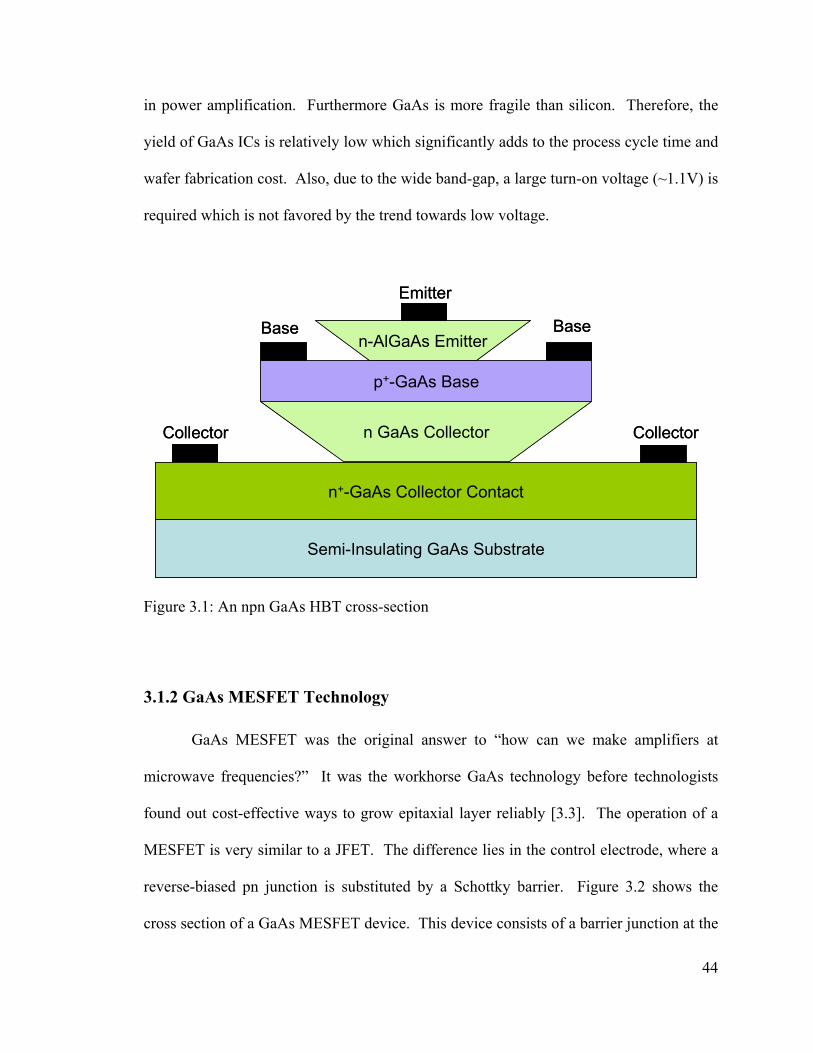
44
in power amplification. Furthermore GaAs is more fragile than silicon. Therefore, the
yield of GaAs ICs is relatively low which significantly adds to the process cycle time and
wafer fabrication cost. Also, due to the wide band-gap, a large turn-on voltage (~1.1V) is
required which is not favored by the trend towards low voltage.
n+-GaAs Collector Contact
Semi-Insulating GaAs Substrate
n GaAs CollectorCollector Collector
p+-GaAs Base
n-AlGaAs EmitterBase
Emitter
Base
n+-GaAs Collector Contact
Semi-Insulating GaAs Substrate
n GaAs CollectorCollector Collector
p+-GaAs Base
n-AlGaAs EmitterBase
Emitter
Base
Figure 3.1: An npn GaAs HBT cross-section
3.1.2 GaAs MESFET Technology
GaAs MESFET was the original answer to “how can we make amplifiers at
microwave frequencies?” It was the workhorse GaAs technology before technologists
found out cost-effective ways to grow epitaxial layer reliably [3.3]. The operation of a
MESFET is very similar to a JFET. The difference lies in the control electrode, where a
reverse-biased pn junction is substituted by a Schottky barrier. Figure 3.2 shows the
cross section of a GaAs MESFET device. This device consists of a barrier junction at the

45
input that acts as a control electrode (or gate), and two ohmic contacts through which
output current flows. The output current varies when the cross section of the conducting
path beneath the gate electrode is changed by changing the negative gate bias.
Very similar to GaAs HBT technology, GaAs MESFET technology usually
features MESFET transistors, thin-film resistors, MIM caps and several metal
interconnect layers. Through-wafer vias are also available in this technology.
Comparing to GaAs HBT technology, MESFET technology is cheaper because no
epitaxial layers are required. However, it requires negative bias for the depletion-mode
transistors to work. These days it is being replaced by GaAs HBT.
Semi-Insulating GaAs Substrate
Source DrainGate
n+-GaAs n+-GaAsn-GaAsp-GaAs
Depletion region
Semi-Insulating GaAs Substrate
Source DrainGate
n+-GaAs n+-GaAsn-GaAsp-GaAs
Depletion region
Figure 3.2: A GaAs MESFET cross-section
3.1.3 GaAs HEMT Technology
HEMT stands for high electron mobility transistor which was invented by Dr.
Takashi Mimura [3.4]. A HEMT is actually a field effect transistor with a junction
between two materials with different band gaps (i.e. a heterojunction) as the channel
instead of an n-doped region. The effect of this junction is to create a very thin layer

46
where the Fermi level is above the conduction band, giving the channel very low
resistance, or in other words “high electron mobility”. Figure 3.3 shows the cross section
of a GaAs HEMT. As with MESFETs, a negative bias is required for depletion-mode
transistors to work. As the HEMT technology developed, the details of the device layer
structure also evolved [3.5]. In fact, the original GaAs/AlGaAs HEMT is now obsolete.
Semi-Insulating GaAs Substrate
Non-doped GaAs
Source Drain
n+ AlGaAsGate
Electron Layer
Figure 3.3: A GaAs/AlGaAs HEMT cross-section
Usually the two different materials used for a heterojunction should have the same
spacing between atoms (lattice constant). Any mismatch will cause discontinuities at the
interface which act as a kind of “trap”, which greatly reduce device performance.
However, PHEMT (Figure 3.4), standing for pseudomorphic high electron mobility
transistor, is a HEMT which violates this rule. It turned out that it is also possible to
grow such heterostructure from materials with different natural lattice constants provided
the thickness of the grown layer does not exceed a critical value. If the grown layer is
thinner than the critical value tc , its crystalline structure conforms to that of the substrate
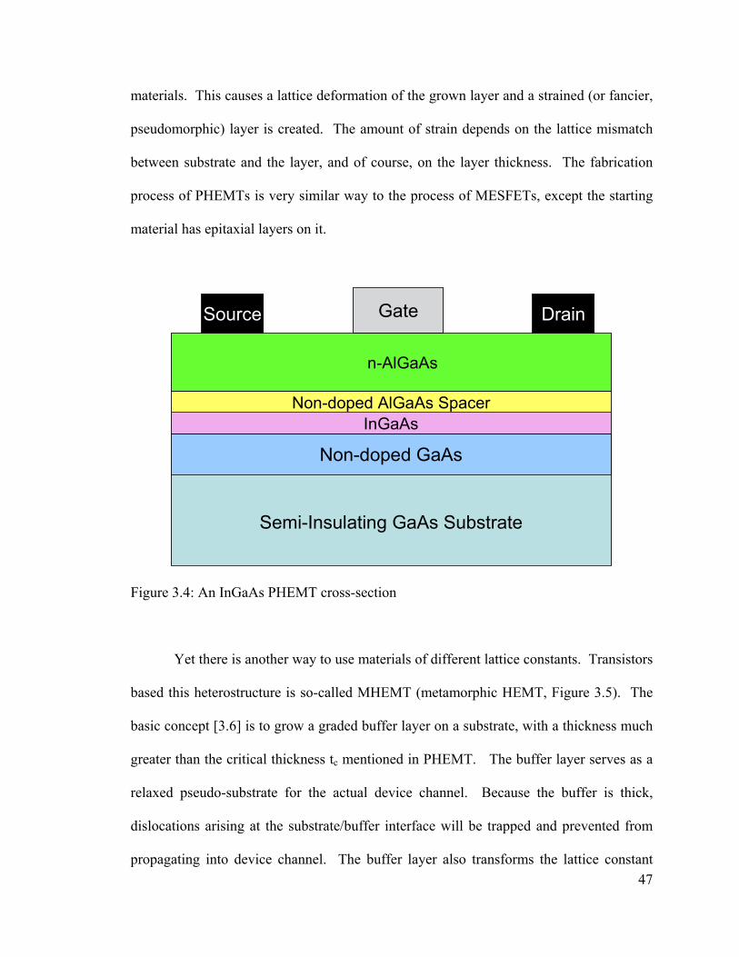
47
materials. This causes a lattice deformation of the grown layer and a strained (or fancier,
pseudomorphic) layer is created. The amount of strain depends on the lattice mismatch
between substrate and the layer, and of course, on the layer thickness. The fabrication
process of PHEMTs is very similar way to the process of MESFETs, except the starting
material has epitaxial layers on it.
n-AlGaAs
Semi-Insulating GaAs Substrate
Non-doped GaAs
Source DrainGate
InGaAsNon-doped AlGaAs Spacer
Figure 3.4: An InGaAs PHEMT cross-section
Yet there is another way to use materials of different lattice constants. Transistors
based this heterostructure is so-called MHEMT (metamorphic HEMT, Figure 3.5). The
basic concept [3.6] is to grow a graded buffer layer on a substrate, with a thickness much
greater than the critical thickness tc mentioned in PHEMT. The buffer layer serves as a
relaxed pseudo-substrate for the actual device channel. Because the buffer is thick,
dislocations arising at the substrate/buffer interface will be trapped and prevented from
propagating into device channel. The buffer layer also transforms the lattice constant

48
from that of a GaAs substrate to that of the device layer. These approaches allow
fabricating very fast transistors with “relatively” cheap GaAs substrate. Again, very
similar to GaAs HBT technology, HEMT process usually includes HEMTs, metal
interconnect layers, MIM capacitors, thin-film resistors, through-substrate vias. And they
have the same disadvantage as GaAs MESFET, requiring both positive and negative
supply.
Semi-Insulating GaAs Substrate
Lattice-Changing InAlAs Graded Buffer
InAlAs Buffer
InGaAs Channel LayerInAlAs Spacer
Source DrainGate
Figure 3.5 An InGaAs MHEMT cross-section
3.1.4 Si CMOS Technology
The concept of the MOSFET was actually developed well before the invention
of the bipolar transistor [3.7]. In 1926 patents were issued to Lilienfield for devices that
resembled the modern silicon MOSFET, but which were made from combinations of
materials not including silicon [3.8]. It took another 34 years before Kahng and Atalla

49
successfully built a working MOSFET. Since then, the growth of digital technologies
such as the microprocessor has provided the motivation to advance silicon16 MOSFET
technology faster than any other semiconductor technology. The primary reason for the
success of Si MOSFET technology is the development of CMOS logic, since Si
MOSFET technology can provide both n-channel and p-channel MOSFET with
comparable performance. However, the MOSFET’s strengths as the workhorse transistor
in most digital circuits did not translate into its supremacy in RF circuits until recently
[3.9].
The MOSFET actually has four terminals: source, drain, gate and back gate.
Figure 3.6 shows the cross section view of a typical CMOS process. Physically, the
operation of the MOSFET can be understood in terms of water analogy [3.7]. The free
carriers correspond to water droplets. The source and drain are deep reservoirs whose
relative elevation difference is like a canal with a depth that depends on the local value of
the gate-to-channel voltage. In a NMOS transistor, if the voltage on the gate increases,
the majority carriers (holes) will be pushed away towards substrate, and be depleted as
gate voltage continues to increase. Eventually, generations of carriers will exceed
recombination. The generated hole-electron pairs are separated by the field, the holes
being swept into the bulk and the electrons moving to the oxide-silicon interface where
they are held because of the energy barrier between the conduction band in the silicon
and that in the oxide. When a drain-to-source voltage is imposed, the current will flow in
the channel. As the drain-to-source voltage increases, the current also increases. Beyond
a certain drain-to-source voltage, the current will saturate.
16 Silicon is exclusively used for manufacturing MOS transistors because of silicon dioxide superior qualities as an insulator.
50
An unwanted byproduct of the bulk-Si CMOS structure is a pair of parasitic
bipolar transistors, forming a parasitic pnpn path as shown in Figure 3.7(a), a basic p-
substrate CMOS cross section. Vertical PNP transistors are formed by a p-substrate, an
n-well, and a p-source or drain and lateral NPN transistors are formed by an n-source or
n-drain, a p-substrate and an n-well. The collector of each BJT is connected to the base
of the other bipolar transistor, forming a positive feedback structure. In order for latch-up
to occur, the structure must be regenerative, in that it must provide a mechanism to
increase the internal current to high values after it exceeds a certain threshold condition.
In addition, external network must be capable of supplying current required by the
regeneration. A two-transistor model, as shown in Figure 3.7(b), was proposed to explain
how latch-up is triggered [3.11]. Usually the gain of parasitic transistor structures is
typically more than sufficient to allow latch-up to occur. It is the presence of the
shunting parasitic resistor (Rwell, Rsub) between the base-emitter junctions that reduces the
regeneration conditions in the parasitic devices with sufficient gain to otherwise exhibit
latch-up. Substrate and n-well are heavily doped to reduce the resistance of Rwell and Rsub.
This effectively reduces the voltage drop across base-emitter junctions with the same
current, which means more current is needed to trigger latch-up. Hence state-of-the-art
bulk-Si CMOS processes use heavily doped silicon substrate to prevent latch-up and
improve yield. However, this causes detrimental impact to lower passive components
quality factor. This will be addressed in detail later.
State-of-the-art digital CMOS technologies usually feature NMOS and PMOS
transistors with different threshold voltages, bipolar devices with reasonable quality,
poly-silicon resistors, more then 6 levels interconnect metal layers with a relatively thick
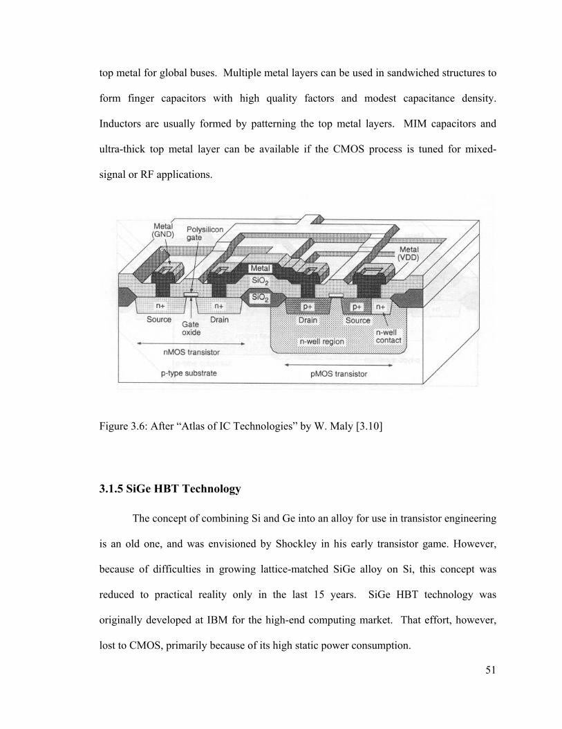
51
top metal for global buses. Multiple metal layers can be used in sandwiched structures to
form finger capacitors with high quality factors and modest capacitance density.
Inductors are usually formed by patterning the top metal layers. MIM capacitors and
ultra-thick top metal layer can be available if the CMOS process is tuned for mixed-
signal or RF applications.
Figure 3.6: After “Atlas of IC Technologies” by W. Maly [3.10]
3.1.5 SiGe HBT Technology
The concept of combining Si and Ge into an alloy for use in transistor engineering
is an old one, and was envisioned by Shockley in his early transistor game. However,
because of difficulties in growing lattice-matched SiGe alloy on Si, this concept was
reduced to practical reality only in the last 15 years. SiGe HBT technology was
originally developed at IBM for the high-end computing market. That effort, however,
lost to CMOS, primarily because of its high static power consumption.
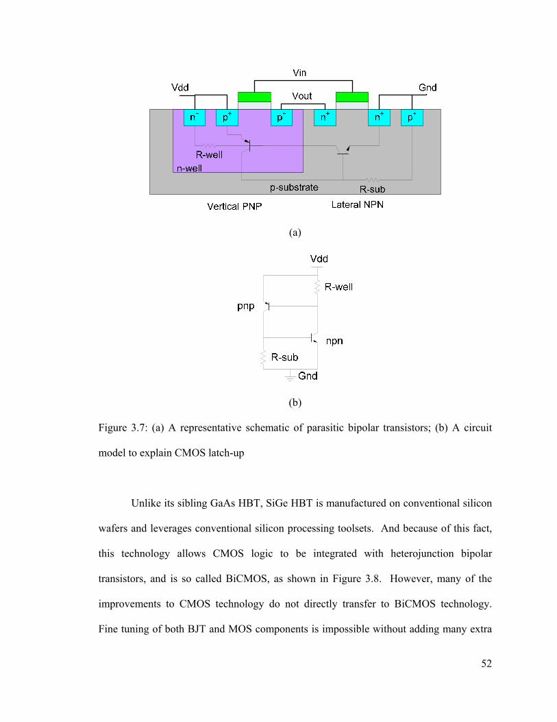
52
(a)
(b)
Figure 3.7: (a) A representative schematic of parasitic bipolar transistors; (b) A circuit
model to explain CMOS latch-up
Unlike its sibling GaAs HBT, SiGe HBT is manufactured on conventional silicon
wafers and leverages conventional silicon processing toolsets. And because of this fact,
this technology allows CMOS logic to be integrated with heterojunction bipolar
transistors, and is so called BiCMOS, as shown in Figure 3.8. However, many of the
improvements to CMOS technology do not directly transfer to BiCMOS technology.
Fine tuning of both BJT and MOS components is impossible without adding many extra
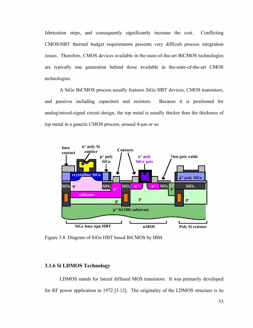
53
fabrication steps, and consequently significantly increase the cost. Conflicting
CMOS/HBT thermal budget requirements presents very difficult process integration
issues. Therefore, CMOS devices available in the-state-of-the-art BiCMOS technologies
are typically one generation behind those available in the-state-of-the-art CMOS
technologies.
A SiGe BiCMOS process usually features SiGe HBT devices, CMOS transistors,
and passives including capacitors and resistors. Because it is positioned for
analog/mixed-signal circuit design, the top metal is usually thicker than the thickness of
top metal in a generic CMOS process, around 4-µm or so.
Figure 3.8: Diagram of SiGe HBT based BiCMOS by IBM
3.1.6 Si LDMOS Technology
LDMOS stands for lateral diffused MOS transistors. It was primarily developed
for RF power application in 1972 [3.12]. The originality of the LDMOS structure is its
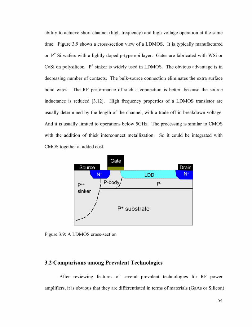
54
ability to achieve short channel (high frequency) and high voltage operation at the same
time. Figure 3.9 shows a cross-section view of a LDMOS. It is typically manufactured
on P+ Si wafers with a lightly doped p-type epi layer. Gates are fabricated with WSi or
CoSi on polysilicon. P+ sinker is widely used in LDMOS. The obvious advantage is in
decreasing number of contacts. The bulk-source connection eliminates the extra surface
bond wires. The RF performance of such a connection is better, because the source
inductance is reduced [3.12]. High frequency properties of a LDMOS transistor are
usually determined by the length of the channel, with a trade off in breakdown voltage.
And it is usually limited to operations below 5GHz. The processing is similar to CMOS
with the addition of thick interconnect metallization. So it could be integrated with
CMOS together at added cost.
P+ substrate
Source DrainGate
P++
sinker
LDDN+ N+
P-body P-
Figure 3.9: A LDMOS cross-section
3.2 Comparisons among Prevalent Technologies
After reviewing features of several prevalent technologies for RF power
amplifiers, it is obvious that they are differentiated in terms of materials (GaAs or Silicon)

55
and devices (BJT or MOSFET). By the late 1990’s, GaAs semiconductor had taken over
more than half of the handset PA market, with silicon LDMOS and bipolar accounting
for the rest. Figure 3.10 shows today’s handset PA market share with GaAs market share
increasing to about 80%. In the wireless LAN PA market, SiGe BJT and CMOS are the
major players in 2.4 GHz applications, while GaAs dominates the 5.2 GHz arena. Before
comparing different technologies, Table 3.1 summarizes the most important properties of
Si and GaAs. In the following, comparisons will be made among four technologies, Si
CMOS, Si LDMOS, SiGe BiCMOS, and GaAs HBT, from several perspectives. At the
end, Table 3.2 will summarize this section.
Material Si GaAs
Band Gap (eV) 1.12 1.43
Breakdown field (V/cm) 3·105 4·105
Saturated Electron Drift Velocity (cm/sec) 1·107 1·107
Thermal Conductivity (W/cm-°C @ RT) 1.5 0.55
Table 3.1: Material properties of Si and GaAs
AlGaAs/InGaP HBT GaAs
LDMOS Si
PHEMT/MESFET GaAs
Other (SiGe BJT…)
AlGaAs/InGaP HBT GaAs
LDMOS Si
PHEMT/MESFET GaAs
Other (SiGe BJT…)
Figure 3.10: Handset PA market share as of 2004 (courtesy of Rob McMorrow)
56
3.2.1 Substrate
In GaAs HBT technologies, a semi-insulating substrate is used as the starting
material. So devices fabricated on such a substrate will have good isolation. Moreover,
semi-insulating substrates provide greatly reduced parasitic capacitances, thus faster
devices. The down side is the thermal conductivity of the substrate used in GaAs
processes. It is especially a problem in power applications.
Very low resistivity substrate is desirable in Si LDMOS technologies, on the
order of 0.007 Ω-cm. This highly conductive substrate is favored because bulk-source
can be tied together to reduce required bond wires and lower the source parasitic
inductance for better performance. State-of-the-art Si CMOS and SiGe BiCMOS
technologies usually adopt silicon substrate with resistivity on the order of 1 Ω-cm in
non-epi processes. Much lower resistivity substrates (~0.01 Ω-cm) are used in epi
processes for digital circuits to avoid latch-up and improve yield.
Unfortunately this conductive substrate causes a headache in designing high
quality factor passives. It is known that the skin depth δ of a substance is the distance to
which incident electromagnetic radiation penetrates [3.13]:
µσωδ 2=
Where µ is the permeability, σ is the electrical conductivity, and ω is the frequency of
interest. Assuming that the substrate resistivity in the selected Si CMOS technology is
0.01 Ω-cm, and the frequency of the application is at 1GHz. The corresponding skin
depth is only 159 µm. Because actual substrate thickness (after thinning) is thicker than
this value, its effect on magnetic field and eddy current induced loss should be considered.
57
Meanwhile, displacement currents flowing into the conductive substrate further increase
loss. From this perspective, GaAs technologies are definitely favored.
3.2.2 Backside Vias
As mentioned previously, GaAs technologies usually feature backside vias that
connect the front side metallization layers of the die to the back side ground plane. It is a
critical element for MMIC technology. Electrically it provides a low resistance and low
inductance (~20-pH) path to the common ground plane. At the same time, it also serves
as a heat dissipation path because GaAs is not a good thermal conductor. Usually in a
GaAs technology process, wafer substrate will be thinned to 30~50 µm before backside
via etching steps. Thinning the substrate makes backside via etching practical and
affordable.
In Si processes, typical substrate thickness varies from 300~800-µm. Therefore it
is not realistic to etch through the wafer substrate with good yield. Thus, ground
connections are realized using bondwires from pad on-chip to the package. In general,
these bondwires have relatively large inductance 17 (~1nH) which is certainly not
desirable in RF applications. To minimize parasitic inductance, two approaches could be
used. One is to increase the diameter of the wire to reduce self-inductance. The other
one is to use several bondwires in parallel to reduce the parasitic inductance. The
ultimate limit of the latter approach is the mutual inductance among wires.
Lower parasitic inductance is very desirable in RF design. Better stability, higher
gain, and other performance improvements could be obtained with lower parasitic
17 The actual inductance depends on the loop.

58
inductance. The availability of backside vias in GaAs technologies was clearly a winner
in the old days when single-ended power amplifiers prevailed. In Si technologies, flip
chip packaging can be employed to achieve low parasitic inductance (~100-pH), but with
much higher cost.
3.2.3 Passives
In analog/RF design, all the glory goes to the sophisticated high gain amplifiers,
however, they are useless without passives to control/tune them. In a typical off-the-shelf
cell phone, a passive to active component ratio of 20:1 is usual. A good portion of those
passives are surface mount passives. To reduce the form factors of handheld devices, the
growing trend is to have as many integrated on-chip as possible.
3.2.2.1 Resistors
Resistors are often used in power amplifiers, and all other analog and mixed-
signal circuit blocks. For bipolar power amplifiers, emitter ballasting resistors are used to
equalize current flow in unit devices. It is also often used to stabilize the circuit, and/or
to bias up circuits. In GaAs technologies, precision thin film resistors with low tolerance,
low parasitics and the ability to make the design changes with short cycle time are
available. Resistors made of active layers are also available to designers. In Si
technologies, doped/undoped poly resistors, diffusion resistors are usually available for
designing circuits. However, precision BEOL (Back-end of the Line) thin film resistors
are not at designers’ hand in general.
59
3.2.2.2 Capacitors
To designers, three characteristics are of particular interests, capacitance density,
parasitic capacitance to the substrate, and the quality factor. MIM capacitors and finger
capacitors are available in both GaAs technologies and Si technologies. Because high-k
dielectrics are used in MIM capacitors and many levels of metallization layers are
available for finger capacitors in Si technologies, the capacitance density is usually much
higher than it is in GaAs technologies. In Si technologies, designers are bothered with
parasitic capacitance to the substrate because it is conductive. However if the capacitor is
used as a part of a tuned tank, the stray capacitance could be absorbed into the tank.
Nonetheless, the extra loss by displacement current in the conductive substrate degrades
the quality factor of capacitors in Si technologies.
Figure 3.11 shows the schematic of a cross-section of a MIM cap [3.14] and the
schematic of a cross-section of a finger cap [3.15]. In Si technologies, the capacitance
density of MIM cap can reach 3~5-fF/µm2, with Q above 100 at 2-GHz range. For finger
caps, the capacitance density can reach 1~2-fF/ µm2, with superior Q above 100 at 10-
GHz range. Capacitors in GaAs technologies have similar quality factor but less density
comparing to Si technologies.
(a) (b)(a) (b)
Figure 3.11: The cross section of (a) A MIM capacitor; (b) A finger capacitor
60
3.2.2.4 Inductors
On-chip inductors can be formed by patterning the metal layers in a process.
Usually, to obtain the best available quality factor, top metal layers are preferred for
realizing inductors. Because on-chip capacitors have enough Q for most applications,
high Q inductors have become the “holy grail” in integrated circuits design. In PAs, the
efficiency of a PA is tightly related with the quality factor of inductors used in the design.
Several mechanisms contribute to the loss of on-chip inductors. First and
foremost is the metallization thickness. At low frequencies, the series resistance can be
calculated from the conductor sheet resistance. At microwave frequencies, the skin effect
becomes dominant, further increasing series resistance. The loss due to the finite
conductivity of the conductors is probably the only source of loss in a GaAs technology.
And it contributes significant amount of the loss in a Si technology. In a typical GaAs
technology, thick top metal (8~10 µm) in gold is available. In contrast, top metal around
2 µm thick in copper or aluminum is typical in a standard state-of-the-art Si technology.
Assuming the resistivity of copper is 17 nΩ·m, and the frequency of the interest is 1GHz,
the corresponding skin depth is 2 µm. Therefore, thicker metal will definitely help to
improve the quality factor at GHz range.
For Si technologies, additional significant degradation of inductor quality factor
results from energy coupled in the conductive substrates. The first kind of coupling is
through electrical coupling. Since an on-chip inductor is essentially one plate of a
capacitor, displacement current will flow into the substrate and cause energy loss. To
prevent this current flowing into the substrate, a lower layer of the metallization stacks
could be patterned to act as pseudo-substrate as far as electrical field is concerned [3.16].

61
This improvement is obtained at the cost of lower self-resonance frequency of the
inductor and enhanced frequency dependence of inductance. The second component of
the coupling is magnetic coupling. The magnetic field generated by an inductor will
induce an image current to flow in the lossy substrate. In the-state-of-the-art Si
technologies, the skin depth of the substrate is thinner than the substrate thickness,
therefore the effect of eddy current cannot be overlooked. Even if the substrate thickness
is slightly thinner than the skin depth, the loss would be nearly the same. Some measures
have been proposed to prevent image current in the substrate [3.17], although the
effectiveness of those measures is in debate.
Due to loss mechanisms mentioned above, the quality factor of an optimized
inductor in Si technologies is around 10 at 2-GHz range. Meanwhile, the quality factor
above 30 could be realized in GaAs technologies. Since high Q passives are crucial to
achieve efficient PAs, GaAs technologies outperform Si technologies without any doubt
from this aspect.
3.2.3 Device characteristics
Even though the physics of MOSFET and BJT are fundamentally different, they
can be designed in circuits with similar topology/architecture to achieve certain
functionality. Two parameters are often cited when comparing devices for RF
applications, namely fT and fmax [3.18]. The fT is defined as the frequency where the
magnitude of the short-circuit common-source/common-emitter current gain falls to unity.
The fT is bias dependent. For MOSFET (small signal model shown in Figure 3.12), it can
be expressed as:
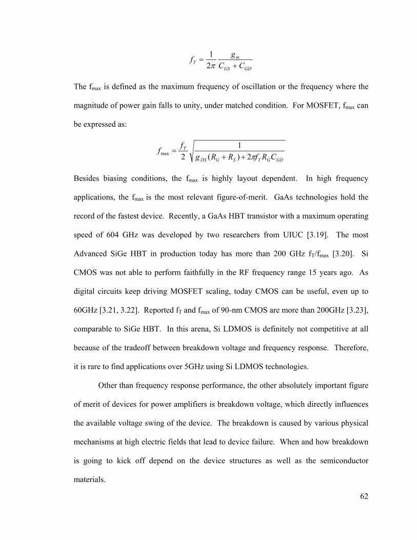
62
GDGS
mT CC
gf+
=π21
The fmax is defined as the maximum frequency of oscillation or the frequency where the
magnitude of power gain falls to unity, under matched condition. For MOSFET, fmax can
be expressed as:
GDGTSGDS
T
CRfRRgff
π2)(1
2max ++=
Besides biasing conditions, the fmax is highly layout dependent. In high frequency
applications, the fmax is the most relevant figure-of-merit. GaAs technologies hold the
record of the fastest device. Recently, a GaAs HBT transistor with a maximum operating
speed of 604 GHz was developed by two researchers from UIUC [3.19]. The most
Advanced SiGe HBT in production today has more than 200 GHz fT/fmax [3.20]. Si
CMOS was not able to perform faithfully in the RF frequency range 15 years ago. As
digital circuits keep driving MOSFET scaling, today CMOS can be useful, even up to
60GHz [3.21, 3.22]. Reported fT and fmax of 90-nm CMOS are more than 200GHz [3.23],
comparable to SiGe HBT. In this arena, Si LDMOS is definitely not competitive at all
because of the tradeoff between breakdown voltage and frequency response. Therefore,
it is rare to find applications over 5GHz using Si LDMOS technologies.
Other than frequency response performance, the other absolutely important figure
of merit of devices for power amplifiers is breakdown voltage, which directly influences
the available voltage swing of the device. The breakdown is caused by various physical
mechanisms at high electric fields that lead to device failure. When and how breakdown
is going to kick off depend on the device structures as well as the semiconductor
materials.
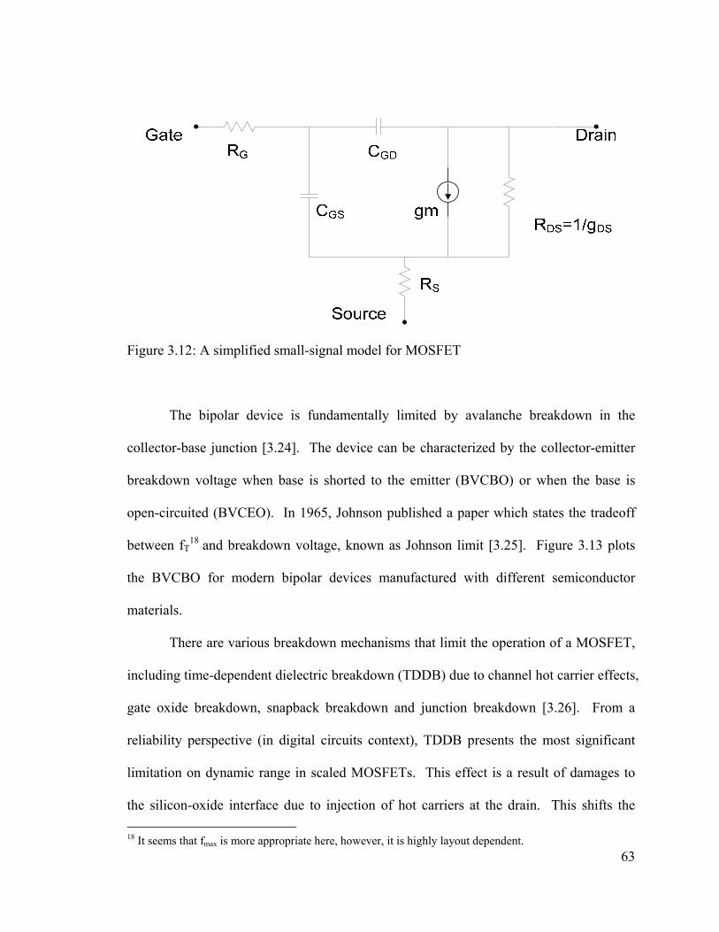
63
Figure 3.12: A simplified small-signal model for MOSFET
The bipolar device is fundamentally limited by avalanche breakdown in the
collector-base junction [3.24]. The device can be characterized by the collector-emitter
breakdown voltage when base is shorted to the emitter (BVCBO) or when the base is
open-circuited (BVCEO). In 1965, Johnson published a paper which states the tradeoff
between fT18 and breakdown voltage, known as Johnson limit [3.25]. Figure 3.13 plots
the BVCBO for modern bipolar devices manufactured with different semiconductor
materials.
There are various breakdown mechanisms that limit the operation of a MOSFET,
including time-dependent dielectric breakdown (TDDB) due to channel hot carrier effects,
gate oxide breakdown, snapback breakdown and junction breakdown [3.26]. From a
reliability perspective (in digital circuits context), TDDB presents the most significant
limitation on dynamic range in scaled MOSFETs. This effect is a result of damages to
the silicon-oxide interface due to injection of hot carriers at the drain. This shifts the 18 It seems that fmax is more appropriate here, however, it is highly layout dependent.
64
threshold voltage of the device and causes oxide quality degradation over an extended
period of time. The recommended voltage limitations are typically based on dc or
transient reliability tests on minimum channel length devices, whereas few results are
available studying device performance degradation under RF operations, or studying
reliability of devices with slightly relaxed channel length19. Although it is believed that
further investigations, to assess reliability and lifetime of devices under RF operations,
can relax the conservative upper limits on the supply voltage for MOSFETs, current
designs in production have to obey the stringent reliability constraints on supply voltage.
A comparison of the BVCBO of bipolar transistors and the recommended
operating voltage for MOSFETs as a function of fT is shown in Fig 3.13. Benefited from
wide band gap as well as high carrier mobility, GaAs HBT is clearly the star in this arena.
And Si CMOS technologies obviously lag behind other technologies. It should be noted
that LDMOS does exhibit excellent performance in terms of breakdown voltage, since
the device is specifically tailored for power applications.
3.2.4 Manufacturing Cost
High-volume proliferation of semiconductor products largely relies on costs being
significantly reduced. Reducing manufacturing cost involves increasing chip yield,
reducing cycle time, maintaining consistent product quality, improving equipment
reliability, and maintaining stringent process control.
GaAs wafers are very brittle and fragile; often require modification to equipment
to prevent wafer breakage. And because of that, GaAs wafers have only recently become 19 From communications with engineers in foundries, supply voltage can be boosted with non-minimum channel length transistors. However, such information cannot be obtained from a design kit.
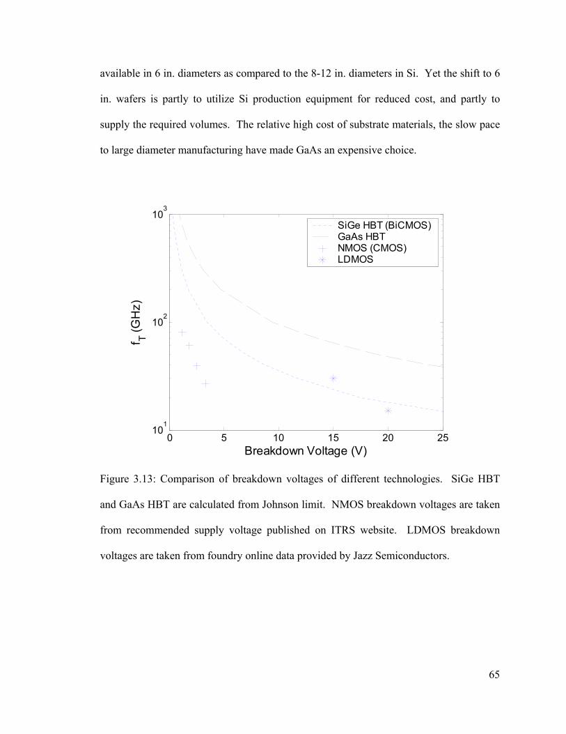
65
available in 6 in. diameters as compared to the 8-12 in. diameters in Si. Yet the shift to 6
in. wafers is partly to utilize Si production equipment for reduced cost, and partly to
supply the required volumes. The relative high cost of substrate materials, the slow pace
to large diameter manufacturing have made GaAs an expensive choice.
0 5 10 15 20 2510
1
102
103
Breakdown Voltage (V)
f T (GH
z)
SiGe HBT (BiCMOS)GaAs HBTNMOS (CMOS)LDMOS
Figure 3.13: Comparison of breakdown voltages of different technologies. SiGe HBT
and GaAs HBT are calculated from Johnson limit. NMOS breakdown voltages are taken
from recommended supply voltage published on ITRS website. LDMOS breakdown
voltages are taken from foundry online data provided by Jazz Semiconductors.
66
3.2.5 Integration
Explosive growth in portable communication market has led to consumer demand
for low-cost, small form factor, low power terminals. It has been proved in practice that
high level of integration is the most effective way to provide such a solution. The VLSI
capabilities of CMOS make itself a well-suited vehicle for high integration, since more
and more functionalities are realized in digital domain. In GaAs technologies, hole
mobility is far behind electron mobility, therefore p-type devices are too slow compared
to n-type device. Besides, good quality insulator that is very crucial for MOSFET is not
available in GaAs technologies. Thus Si is an ideal substrate for manufacturing MOS
transistors for digital circuits, while it is extremely difficult to manufacture MOS
Transistors on GaAs substrate. Therefore, Si technology has the potential to deliver a
complete, low cost system
3.2.6 Availability & Capacity
Traditionally, GaAs has been avoided by high-volume semiconductor device
manufacturers in preference to the established silicon CMOS, Bipolar and BiCMOS
designs and processing. Unlike its silicon equivalent, a “pure-play” GaAs foundry does
not exist or at least is very hard to find. It was estimated in 2005 that the overall GaAs
foundry industry is $100 million business [3.27], only 0.3% of DRAM market. And
because it is a small market that is only able to support only a few foundries, GaAs
foundries availability and capacity are very limited. In silicon technology, LDMOS
technologies are also not easy to get access compared to as other silicon technologies. In
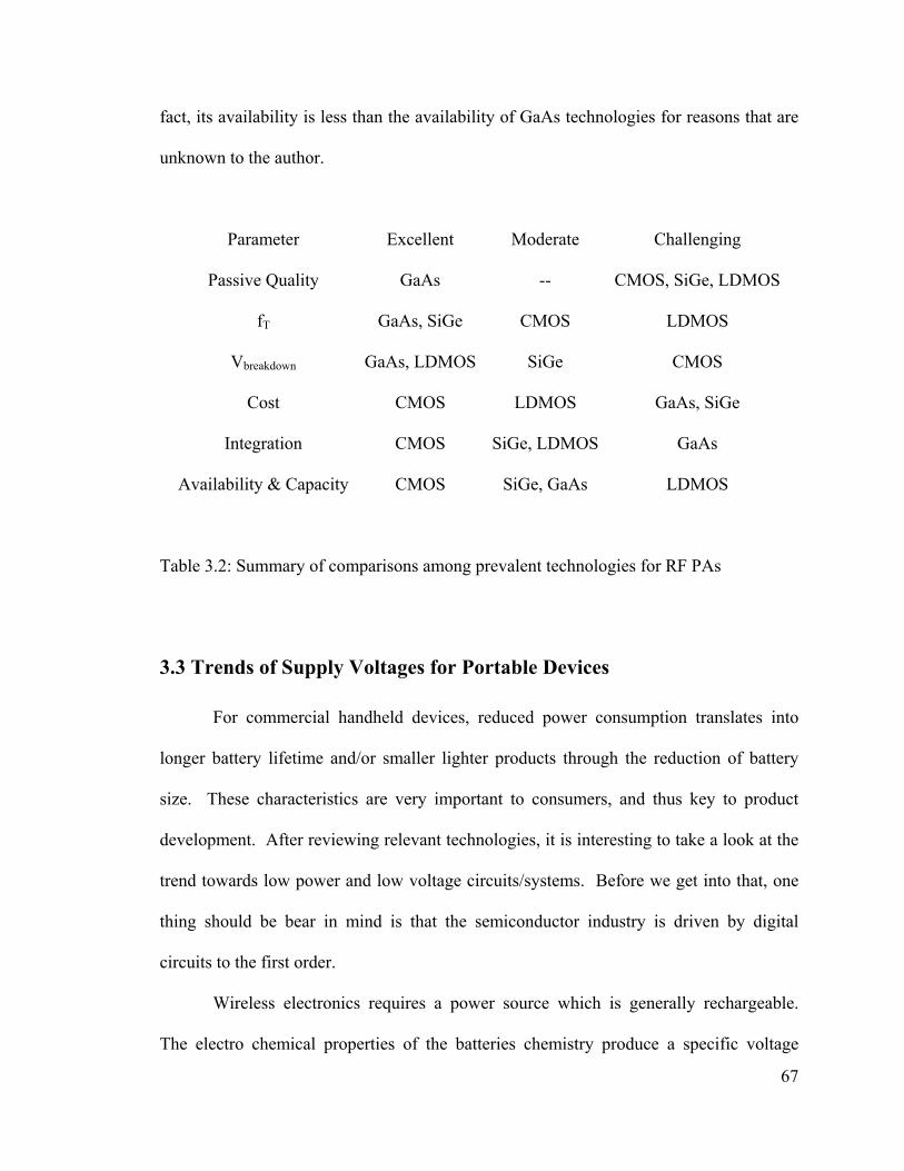
67
fact, its availability is less than the availability of GaAs technologies for reasons that are
unknown to the author.
Parameter Excellent Moderate Challenging
Passive Quality GaAs -- CMOS, SiGe, LDMOS
fT GaAs, SiGe CMOS LDMOS
Vbreakdown GaAs, LDMOS SiGe CMOS
Cost CMOS LDMOS GaAs, SiGe
Integration CMOS SiGe, LDMOS GaAs
Availability & Capacity CMOS SiGe, GaAs LDMOS
Table 3.2: Summary of comparisons among prevalent technologies for RF PAs
3.3 Trends of Supply Voltages for Portable Devices
For commercial handheld devices, reduced power consumption translates into
longer battery lifetime and/or smaller lighter products through the reduction of battery
size. These characteristics are very important to consumers, and thus key to product
development. After reviewing relevant technologies, it is interesting to take a look at the
trend towards low power and low voltage circuits/systems. Before we get into that, one
thing should be bear in mind is that the semiconductor industry is driven by digital
circuits to the first order.
Wireless electronics requires a power source which is generally rechargeable.
The electro chemical properties of the batteries chemistry produce a specific voltage

68
potential which is commonly referred to as a cell. Table 3.3 provides a list of the some of
the main battery technologies for use in portable electronics and their associated
characteristics [3.28]. If the standard single cell voltage of a technology is higher than
the desired operating level, then DC-to-DC conversion will be needed for a lower output
voltage.
Fifteen years ago, power amplifiers in mobile handsets were primarily built using
discrete transistors, operating from either 4.8-V or 6V power sources. Around 1996, a
leading handset provider dropped their battery system down to 3V to reduce the size of
handsets [3.29]. Due to the obvious trend towards low supply voltage, there is an
interesting debate in the industry whether to completely rely on DC-to-DC converter or
develop low cell voltage batteries. From Table 3.3, low cell voltage Li-Polymer battery
is an attractive candidate, which has better energy density with comparable cost. Among
various projections, Figure 3.14 shows the projection of battery voltage from a report
released in 2004 by iNEMI20. Although the projection did not happen as scheduled, it
does show the trend towards low battery voltage. One of the reasons that caused delay,
according to the author’s opinion, is the resistance from PA manufacturers. The
developments of circuits to consume low power at lower supply voltages are consistent
with the general trends of CMOS scaling. For digital circuits, active power consumption
of a chip has quadratic relationship with the supply voltage:
fCVPactive2∝
Smaller devices require less voltage to achieve the same electric field levels, thus reduced
size also leads to reduced voltage requirements. Supply voltage of CMOS is scaled down
20 International Electronics Manufacturing Initiative, an industry-led consortium of approximately 70 electronics manufacturers, suppliers and related organizations, including Intel, IBM, TI.
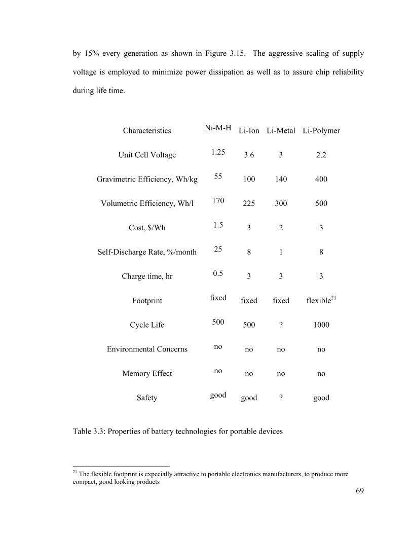
69
by 15% every generation as shown in Figure 3.15. The aggressive scaling of supply
voltage is employed to minimize power dissipation as well as to assure chip reliability
during life time.
Characteristics Ni-M-H Li-Ion Li-Metal Li-Polymer
Unit Cell Voltage 1.25 3.6 3 2.2
Gravimetric Efficiency, Wh/kg 55 100 140 400
Volumetric Efficiency, Wh/l 170 225 300 500
Cost, $/Wh 1.5 3 2 3
Self-Discharge Rate, %/month 25 8 1 8
Charge time, hr 0.5 3 3 3
Footprint fixed fixed fixed flexible21
Cycle Life 500 500 ? 1000
Environmental Concerns no no no no
Memory Effect no no no no
Safety good good ? good
Table 3.3: Properties of battery technologies for portable devices
21 The flexible footprint is expecially attractive to portable electronics manufacturers, to produce more compact, good looking products
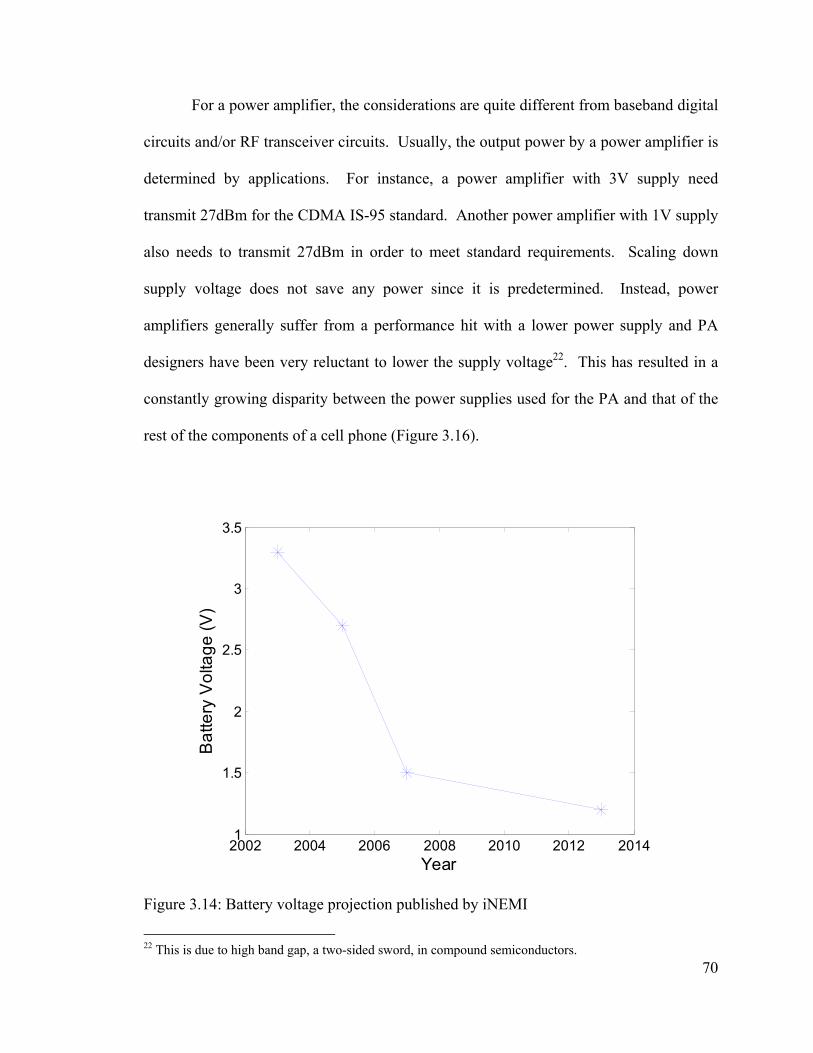
70
For a power amplifier, the considerations are quite different from baseband digital
circuits and/or RF transceiver circuits. Usually, the output power by a power amplifier is
determined by applications. For instance, a power amplifier with 3V supply need
transmit 27dBm for the CDMA IS-95 standard. Another power amplifier with 1V supply
also needs to transmit 27dBm in order to meet standard requirements. Scaling down
supply voltage does not save any power since it is predetermined. Instead, power
amplifiers generally suffer from a performance hit with a lower power supply and PA
designers have been very reluctant to lower the supply voltage22. This has resulted in a
constantly growing disparity between the power supplies used for the PA and that of the
rest of the components of a cell phone (Figure 3.16).
2002 2004 2006 2008 2010 2012 20141
1.5
2
2.5
3
3.5
Year
Bat
tery
Vol
tage
(V)
Figure 3.14: Battery voltage projection published by iNEMI
22 This is due to high band gap, a two-sided sword, in compound semiconductors.
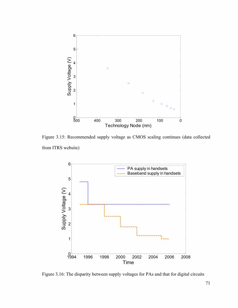
71
01002003004005000
1
2
3
4
5
6
Technology Node (nm)
Sup
ply
Vol
tage
(V)
Figure 3.15: Recommended supply voltage as CMOS scaling continues (data collected
from ITRS website)
1994 1996 1998 2000 2002 2004 2006 20080
1
2
3
4
5
6
Time
Sup
ply
Vol
tage
(V)
PA supply in handsetsBaseband supply in handsets
Figure 3.16: The disparity between supply voltages for PAs and that for digital circuits
72
3.4. Limits of CMOS and the Impact of Scaling
Two major hurdles associated with the design of fully integrated power amplifiers
are low transistor breakdown voltage/high threshold voltage, and high loss impedance
transformation network consisting of lossy on-chip passives. The limitations are from
semiconductor materials as well as device structures. In this section, challenges and
opportunities presented by the continued scaling will be studied with data from ITRS
[3.30].
3.4.1 Device Scaling
For devices available in today’s technologies, GaAs or Silicon, MOSFET or HBT,
they all have enough capabilities to be designed to operate at a few tens of GHz range.
With respect to MOSFET devices for power amplifiers, frequency response is probably
the only thing that will benefit from scaling. Other metrics such as linearity will
inevitably degrade as scaling continues [3.31]. Fortunately technology scaling
significantly lowers the cost of digital logic and memory, leveraging digital baseband
processing power to improve the PA linearity demonstrates great potential. For example,
predistortion techniques have been adopted in base station to improve the linearity of the
PA [3.32]. As scaling continues, it will take less power and area to implement
predistortion technique, making it suitable for portable devices as well.
As shown in chapter 2, the importance of large voltage swing at the output needs
no introduction. A serious issue that designers have to face is the ever-decreasing voltage
headroom which severely limits the power handling capability and the efficiency of
power amplifiers. Although state-of-the-art CMOS technologies offer several thin-oxide

73
devices, with different threshold voltages and RF design usually pick low threshold
voltage devices to maximize swing, the scaling of threshold voltage cannot track the
scaling of the supply voltage because of the requirements to control the leakage power.
This trend will continue in the future as predicted by ITRS (Figure 3.17). Today’s state-
of-the-art CMOS technologies offer I/O transistors with relaxed channel length and gate
dielectric thickness. Strategic adoption of these I/O transistors might overcome some of
the voltage limitations. However, there are several issues here. First, the device
modeling of the I/O transistors may not be well characterized as the core transistors. And
the process control is tuned for the core transistors instead of I/O transistors. Moreover,
I/O transistors also scale with core transistors. The supply voltage for I/O devices will
follow the scaling of supply voltage of core devices, maybe with different factor (Figure
3.17).
2003 2004 2005 2006 2007 2008 2009 2010 2011 20120
0.5
1
1.5
2
2.5
3
3.5
Time
Vol
tage
(V)
Threshold Voltage (low Vt devices)Supply Voltage (high performance logic)Supply Voltage (I/O devices)
Figure 3.17: Scaling of supply voltages and threshold voltage for analog/RF circuits

74
3.4.2 Starting Materials
Historically, CMOS devices are fabricated using starting materials involved the
choice of either polished Czochralski (CZ, non-epi) or epitaxial silicon wafers. Recently,
silicon-on-insulator (SOI) wafers have become more than a niche technology, although
the total number of SOI wafers shipped is still small compared to non-epi and epi wafers.
The opportunity for SOI wafers to be used in mainstream high-volume application is
being driven by improved high frequency logic performance and reduced power
consumption, as well as enhanced device performance via unique device configurations
such as multiple-gate transistor structure. In some cases, process flow simplification is
also achieved. Meanwhile, the implementation of shallow trench isolation (STI) and the
development of alternate doping means for achieving latch-up suppression make a
heavily doped substrate as starting material unnecessary23. The possibility of eliminating
conductive substrate would greatly reduce losses induced by lossy substrate, hence
improving the quality factor of on-chip passives.
3.4.3 Metal Stack Scaling
In CMOS scaling, critical dimensions of active devices are scaling down.
However, metal stack is scaled inversely. For example, number of metal layers increase
with technology scaling (Figure 3.18). Meanwhile, low-k inter-metal dielectrics and
copper are replacing conventional silicon-dioxide and aluminum in the metal stack. This
metallization scheme is to minimize RC delay and voltage drop across the chip for those
global interconnects and power grids in digital circuits. Nonetheless, the impact of
23 From cost perspective, an epitaxial wafer is more expensive than a non-epi wafer.

75
interconnect scaling on passive device quality is unclear at this point. For example, in a
typical 0.35-µm process, there are four metal layers, with the top layer about 1-µm thick,
and about 6-µm above the substrate. State-of-the-art 90-nm technology typically offers 7
metal layers, but only with the top layer about 0.9-µm thick, and about 5~6-µm above the
substrate. Therefore, it is likely that the quality of passives may degrade24.
0
1
2
3
4
5
6
7
8
Technology Node (nm)
Num
ber o
f Met
al L
ayer
s
350 250 180 130 90 65
Figure 3.18: Number of Metallization layers vs. technology node
3.5 Summary
Because wireless device suppliers consistently face savvy consumers’ demands
for higher performance, lower costs and faster design turnaround, they are compelled to
24 RF CMOS processes provide thick top metal (2~4-µm), but with added cost.
76
rely more and more on their component suppliers to provide a system solution. As a
result, part of this onus is passed on to component suppliers to help meet end-user needs
including smaller size, enhanced performance, longer battery life, and lower prices. One
way to meet these demands is by modifying manufacturing processes or changing
manufacturing technologies used to fabricate RF power amplifiers. CMOS has proven
itself a suitable vehicle to meet such stringent requirements. From performance and
power dissipation perspective, data transfer on-chip can be significantly faster than off
chip and requires less power. From cost perspective, it might be true that fully integrated
system is not the cheapest solution at present time. However, it offers great potential for
cost saving in the future.
3.6 References
[3.1] W. SHOCKLEY, US Patent #02569374, filed June 26th 1948.
[3.2] P.A. Houston, “High-frequency Heterojunction Bipolar Transistor Device Design
and Technology”, Electronics &Communication Eng. J., Vol. 12, No. 5, pp. 220-228,
October, 2000
[3.3] G. Nuzillat, E.H. Perea, G. Bert, F. Damay-Kavala, M. Gloanec, M. Peltier, T.P.
Ngu, C. Arnodo, “GaAs MESFET ICs for gigabit logic applications”, IEEE J. Solid-State
Circuits, vol. 17, no. 3, pp. 569-584, June 1982
[3.4] T. Mimura, “Development of High Electron Mobility Transistor”, Jpn J. Appl.
Phys., vol. 44, no. 12, pp.8263-8268, 2005
[3.5] D. Docter, M. Matlouvian, M. Micovic, C. Nguyen, C. Ngo, S. Bui, P. Janke, “Next
Generation HEMTs”, Device Research Conference Digest, pp146-149, 28-30 June 1999

77
[3.6] C.S. Whelan, P.F. Marsh, W.E. Hoke, R.A. McTaggart, C.P. McCarroll, T.E.
Kazior, “GaAs metamorphic HEMT (MHEMT): an attractive alternative to InP HEMT
for high performance low noise and power applications”, Proc. Intl. Conference on
Indium Phosphide and Related Materials, pp. 337-340, May 2000
[3.7] R.S. Muller, T.I. Kamins, “Device Electronics for Integrated Circuits”, 2nd Edition,
John Wiley & Sons, Inc. 1986.
[3.8] J.E. Lilienfield, US Patent #1900018, 1926.
[3.9] A.A. Abidi, “ RF CMOS comes of age”, IEEE J. Solid-State Circuits, vol. 39, no. 4,
pp. 549-561, 2004
[3.10] W. Maly, “Atlas of IC technologies: An Introduction to VLSI Processes”, CA:
Benjamin/Cummings, 1987
[3.11] B.L. Gregory, B.D. Shafer, “Latchup in CMOS integrated circuits”, IEEE Trans.
Nucl. Sci., vol. NS-20, no. 6, pp. 293-299, 1973
[3.12] H.J. Sigg, G.D. Vendelin, T.P. Cauge, J. Kocsis, “D-MOS transistor for
microwave applications”, IEEE Trans. on Electron Devices, vol. 19, no. 1, pp. 45-53,
1972
[3.13] J.D Jackson, “classical Electrodynamics”, 3rd Edition, John Wiley &Sons, Inc.
1999
[3.14] Y.L. Tu, H.L. Lin, L.L. Chao, D. Wu, C.S. Tsai, C. Wang, C.F. Huang, C.H.Lin,
and J.Y.-C. Sun, “Characterization and comparison of high-k metal-insulator-metal
(MIM) capacitors in 0.13 µm Cu BEOL mixed-mode and RF applications”, Proc. of
Symp. VLSI Technology, pp. 79-80, 2003

78
[3.15] H. Samavati, A. Hajimiri, G. Nasserbakht, T. Lee, “Fractal capacitors”, Proc. of
ISSCC, pp. 256-257, 1998
[3.16] C.P. Yue, S.S. Wong, “On-chip spiral Inductors with patterned ground shields for
Si-based RF ICs”, IEEE J. Solid-State Circuits, vol. 33, no. 5, pp. 743-752, May, 1998
[3.17] C.A. Chang, S.-P. Tseng, J.Y. Chuang, S.-S. Jiang, J.A. Yeh, “Characterization of
spiral inductors with patterned floating structures”, IEEE MTT, vol. 52, no. 5, pp.1375-
1381, May, 2004
[3.18] P.R. Gray, P.J. Hurst, S.H. Lewis, R.G. Meyer, “Analysis and Design of Analog
Integrated Circuits”, 4th Edition, John Wiley & Sons, Inc. 2001
[3.19] W. Hafez, M. Feng, “Experimental demonstration of pseudomorphic
heterojunction bipolar transistors with cut off frequencies above 600 GHz”, Appl. Phys.
Lett., vol. 86, 152101, 2005
[3.20] D. Harame, “RF Device Technologies”, IEDM Short Course, 2002
[3.21] B. Razavi, “A 60-GHz CMOS receiver front-end”, IEEE J. Solid-State Circuits,
vol. 41, no. 1, pp.17-22, January, 2006
[3.22] C.H. Doan, S. Emami, A.M. Niknejad, R.W. Brodersen, “Millimeter-wave CMOS
design”, IEEE J. Solid-State Circuits, vol. 40, no. 1, pp. 144-155, January 2005
[3.23] K. Kuhn, R. Basco, D. Becher, M. Hattendorf, P. Packan, I. Post, P. Vandervoorn,
I. Young, “A comparison of state-of-the-art NMOS and SiGe HBT devices for
analog/mixed-signal/RF circuit applications”, Digest of Tech. Papers, Symp. on VLSI
Tech, pp.224-225, 2004
[3.24]A. Huang, B. Zhang, “The future of bipolar power tranasistors”, IEEE Trans. Elec.
Devices, vol. 48, pp. 2535-2543, November, 2001

79
[3.25] E.O. Johnson, “Physical limitations on frequency and power parameters of
transistors”, IEEE Intl. Conv. Record, p. 27, 1965
[3.26] J. H. Stathis, “Reliability limits for the gate insulator in CMOS technology”, IBM
Journal of Research and Development, vol. 46, no. 2/3, 2002
[3.27] M. LaPedus, “Consolidation hits GaAs foundry Market”, EE Times, September 07,
2005
[3.28] Bassak, Gil, "Designing Battery-Powered Portable Products: From Concept to
Prototype", EE Product News, March 1996, pg 37.
[3.29] P.J. Augustine, “Trends and Opportunities for Gallium Arsenide Semiconductors
in Handsets”, Proc. IEEE Intl. Conf. on Compound Semiconductor Manufacturing, April,
2005
[3.30] International Technology Roadmap for Semiconductors, http://public.itrs.net/
[3.31] P.H. Woerlee, M.J. Knitel, R. Van Langeveld, D.B.M. Klaassen, L.F. Tiemeijer,
A.J. Scholten, A.T.A. Zegers-van Duijnhoven, “ RF-CMOS performance trends”, IEEE
Tran. On Electron Devices, vol. 48, no. 8, pp. 1776-1782, August, 2001
[3.32] S-Y. Lee, Y-S. Lee, S-H. Hong, H-S. Choi, Y-H. Jeong, “An adaptive
predistortion RF power amplifier with a spectrum monitor for multicarrier WCDMA
applications”, IEEE MTT., vol. 5, no. 2, pp. 786-793, February, 2005

80
Chapter 4: Generating High Power with Low Voltage Devices
4.1 Series power combining
4.2 Parallel power combining
4.3 Proposed power combiner
4.4 Summary
4.5 References
When a larger output is needed than can be obtained from a single device or pair
of devices, multiple devices can be arranged in different ways to achieve the needed
output power. This is precisely the situation that designers have to face when using
CMOS technologies for RF PAs. In this chapter, two kinds of approaches will be
discussed. The first approach, series combining through stacking devices, generates high
output power by connecting devices together in a way so that they can operate reliably
with a supply voltage much higher than recommended voltage. The second approach,
parallel combining, combines power from several small amplifiers to generate high
output power. The two approaches can be used alone, or in conjunction to generate even
higher power.
4.1 Series Power Combining
4.1.1 Cascode Configuration
The cascode configuration was first invented for vacuum-tube circuits. It is
important mostly because it increases output resistance and greatly reduces unwanted
81
capacitive feedback. Therefore, the cascode configuration is generally used in
operational amplifiers and other low-frequency designs. In MOS form, the cascode is a
common-source – common-gate amplifier as shown in Figure 4.1. Only the gate of the
common-source transistor is driven by input signals. The gate of the common-gate
transistor is AC grounded.
In the case of RF power amplifiers, the cascode offers an important additional
benefit. An advantage that the cascode configuration has over single transistor topology
is it can sustain higher voltage before breakdown happens. In a state-of-the-art CMOS
process, junction breakdown voltage is significantly higher than recommended supply
voltage which is primarily determined by drain-to-source breakdown voltage. Therefore,
in principle, the voltage stress could be shared between common-gate and common-
source transistors.
However, the voltage stress is not usually evenly split between two transistors.
Typically, the common-gate transistor is stressed more than the common-source
transistor, depending on the biasing level at the common-gate. Hence it may become the
bottle neck in terms of breakdown. Previous work used a combination of standard thin-
gate-oxide transistors for common-source devices and I/O devices for common-gate
devices to alleviate this problem [4.1]. Unfortunately, a thick-gate-oxide device does not
have comparable high-frequency performance of a standard device. Therefore, the thick-
gate-oxide device degrades the RF gain, and limits other high-frequency performance.
Other work proposed an alternative solution [4.2]. Instead of AC grounding the gate of
the common-gate device, the AC voltage at the gate is set to swing with the same polarity
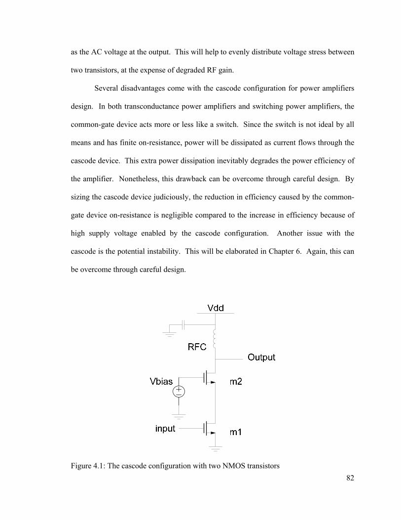
82
as the AC voltage at the output. This will help to evenly distribute voltage stress between
two transistors, at the expense of degraded RF gain.
Several disadvantages come with the cascode configuration for power amplifiers
design. In both transconductance power amplifiers and switching power amplifiers, the
common-gate device acts more or less like a switch. Since the switch is not ideal by all
means and has finite on-resistance, power will be dissipated as current flows through the
cascode device. This extra power dissipation inevitably degrades the power efficiency of
the amplifier. Nonetheless, this drawback can be overcome through careful design. By
sizing the cascode device judiciously, the reduction in efficiency caused by the common-
gate device on-resistance is negligible compared to the increase in efficiency because of
high supply voltage enabled by the cascode configuration. Another issue with the
cascode is the potential instability. This will be elaborated in Chapter 6. Again, this can
be overcome through careful design.
Figure 4.1: The cascode configuration with two NMOS transistors

83
4.1.2 Totem-Pole Technique
The totem-pole amplifier [4.3] is also known as “beanstalk” amplifier. It is a
technique to obtain voltage swing greater than breakdown voltage by placing the output
of several transistors in series as shown in Figure 4.2, so that the individual transistors do
not have to withstand the full voltage swing at the output of the amplifier.
Figure 4.2: Beanstalk amplifier
The name “totem-pole” comes from the bias ladder. The resistors ladder will bias
the circuit up and ensure a predictable division of drain-to-source voltage. For RF or
microwave frequency operation, the signal from the input port would have to propagate
up to the gate. This will cause a delay and imbalance of each device, so that the output is

84
not synchronized to add up in phase. This will degrade output power, power efficiency,
and cause distortion in some applications.
4.1.3 Stacked Transistors Amplifier
To eliminate the high frequency limitation of “bean-stalk” amplifier, McRory et al.
proposed a stacked power amplifier using transformer coupling to supply input signals as
shown in Figure 4.3 [4.4]. The resistors ladder is designed to bias the transistors up.
Capacitors are large enough to be treated as AC short at the frequency of operation. This
will bootstrap the input of each transistor with its source, so that the output swing can
exceed the drain-to-source breakdown voltage as long as it is less than the junction
breakdown voltage.
Figure 4.3: A three FET stacked power amplifier

85
4.2 Parallel Combining
Instead of increasing output swing by combining transistors in series, power could
be combined from several small or unit amplifiers operating in parallel. Apparently
direct connection of multiple small amplifiers is generally impractical as the PAs “talk”
to each other. Interaction among small amplifiers should be judiciously managed so that
outputs from small amplifiers are combined in a healthy fashion. Hence it is necessary to
build power combiners to perform this function. There are many different ways to build
power combiners, using lumped components or distributed approach. Among those,
transmission-line based power combiner and transformer based power combiner are
probably two most popular measures25.
4.2.1 Transformer Based Power Combining
This power combining approach was an old idea since 1960s [4.5]. Since then,
transformers have been widely adopted as a means for splitting or combining RF power.
To illustrate how transformer based power combining works, an example of a two-way
power combined amplifier is used here (Figure 4.4). Two transconductance PAs are
driven 180° out of phase with respect to each other.
For the push-pull operation, the amplitude of I1 equals to that of I2, and the
voltage amplitudes are also equal. It is obvious that
O
O
VnmVV
ImnII
21
21
21
==
==
25 Because those elements are passive in nature, they can often be used to split power as well.
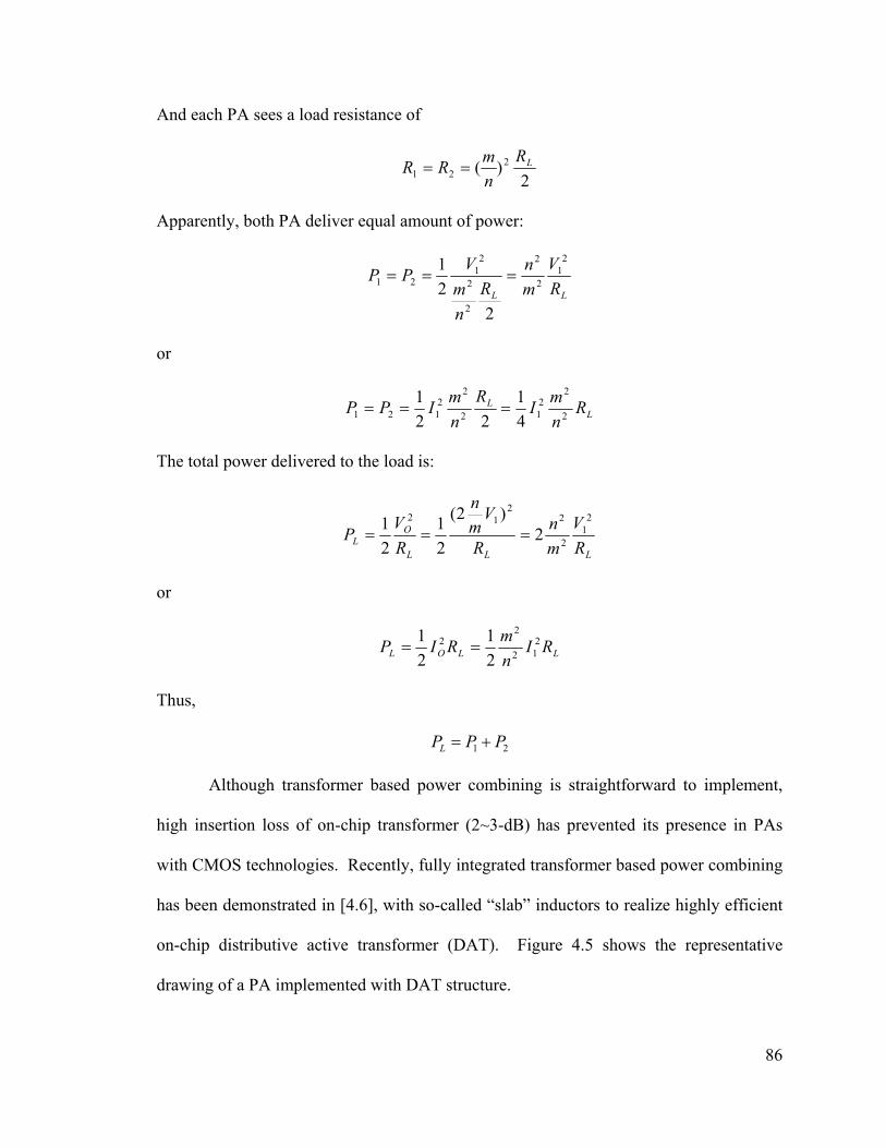
86
And each PA sees a load resistance of
2)( 2
21LR
nmRR ==
Apparently, both PA deliver equal amount of power:
LL RV
mn
Rnm
VPP2
12
2
2
2
21
21
221
===
or
LL R
nmIR
nmIPP 2
22
12
22
121 41
221
===
The total power delivered to the load is:
LLL
OL R
Vmn
R
Vmn
RV
P2
12
22
12
2)2(
21
21
===
or
LLOL RInmRIP 2
12
22
21
21
==
Thus,
21 PPPL +=
Although transformer based power combining is straightforward to implement,
high insertion loss of on-chip transformer (2~3-dB) has prevented its presence in PAs
with CMOS technologies. Recently, fully integrated transformer based power combining
has been demonstrated in [4.6], with so-called “slab” inductors to realize highly efficient
on-chip distributive active transformer (DAT). Figure 4.5 shows the representative
drawing of a PA implemented with DAT structure.
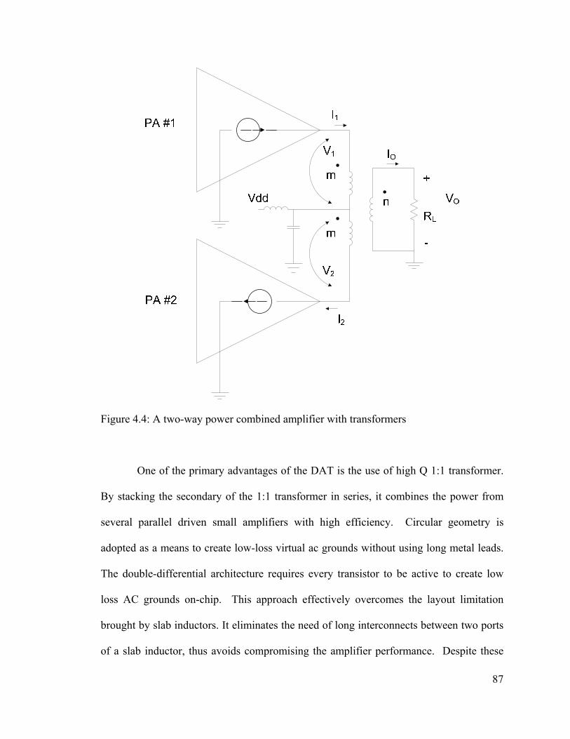
87
Figure 4.4: A two-way power combined amplifier with transformers
One of the primary advantages of the DAT is the use of high Q 1:1 transformer.
By stacking the secondary of the 1:1 transformer in series, it combines the power from
several parallel driven small amplifiers with high efficiency. Circular geometry is
adopted as a means to create low-loss virtual ac grounds without using long metal leads.
The double-differential architecture requires every transistor to be active to create low
loss AC grounds on-chip. This approach effectively overcomes the layout limitation
brought by slab inductors. It eliminates the need of long interconnects between two ports
of a slab inductor, thus avoids compromising the amplifier performance. Despite these
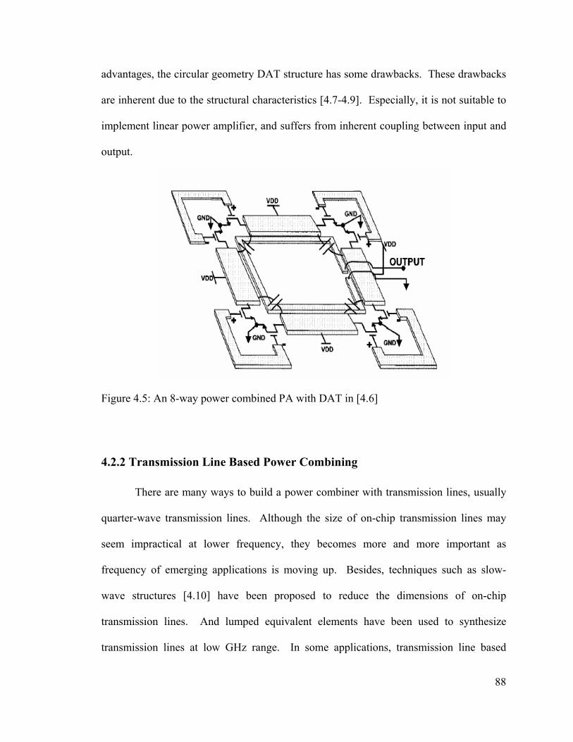
88
advantages, the circular geometry DAT structure has some drawbacks. These drawbacks
are inherent due to the structural characteristics [4.7-4.9]. Especially, it is not suitable to
implement linear power amplifier, and suffers from inherent coupling between input and
output.
Figure 4.5: An 8-way power combined PA with DAT in [4.6]
4.2.2 Transmission Line Based Power Combining
There are many ways to build a power combiner with transmission lines, usually
quarter-wave transmission lines. Although the size of on-chip transmission lines may
seem impractical at lower frequency, they becomes more and more important as
frequency of emerging applications is moving up. Besides, techniques such as slow-
wave structures [4.10] have been proposed to reduce the dimensions of on-chip
transmission lines. And lumped equivalent elements have been used to synthesize
transmission lines at low GHz range. In some applications, transmission line based
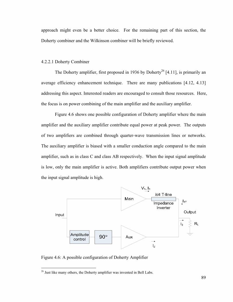
89
approach might even be a better choice. For the remaining part of this section, the
Doherty combiner and the Wilkinson combiner will be briefly reviewed.
4.2.2.1 Doherty Combiner
The Doherty amplifier, first proposed in 1936 by Doherty26 [4.11], is primarily an
average efficiency enhancement technique. There are many publications [4.12, 4.13]
addressing this aspect. Interested readers are encouraged to consult those resources. Here,
the focus is on power combining of the main amplifier and the auxiliary amplifier.
Figure 4.6 shows one possible configuration of Doherty amplifier where the main
amplifier and the auxiliary amplifier contribute equal power at peak power. The outputs
of two amplifiers are combined through quarter-wave transmission lines or networks.
The auxiliary amplifier is biased with a smaller conduction angle compared to the main
amplifier, such as in class C and class AB respectively. When the input signal amplitude
is low, only the main amplifier is active. Both amplifiers contribute output power when
the input signal amplitude is high.
Figure 4.6: A possible configuration of Doherty Amplifier
26 Just like many others, the Doherty amplifier was invented in Bell Labs.

90
To understand how the Doherty amplifier really works, active load-pull technique
should be understood first. Since it is well explained in [4.12], it will not be repeated
here. The operation of the Doherty amplifier can be explained by dividing it into low-
power, medium power and high power region, assuming lossless matching networks.
In the low-power region (Figure 4.7(a)), the instantaneous amplitude of the input
signal is not sufficient to turn on the auxiliary power amplifier, so it will remain off and
appear as an open-circuit without any interaction with the main amplifier. The main
amplifier sees the load inverted by the quarter-wave transmission line and operates
exactly the same as an ordinary power amplifier. The output swing increases linearly
with input until reaching the clipping point. As the input signal amplitude keeps
increasing into the medium-power region, the Doherty amplifier enters into medium-
power region (Figure 4.7(b)). The main amplifier is in the constant maximum voltage
condition, but the effective load decreases dynamically with the increase of the input
signal amplitude due to the load-pulling effect of the auxiliary amplifier. In this region,
the auxiliary amplifier also sees load-pulling effect that the effective load also decreases
with the increase in the input signal amplitude. Finally, when both amplifiers contribute
same amount of power to the load, the Doherty amplifier is in the peak-power mode
(Figure 4.7(c)). Note the importance of a quarter-wave transmission line between the
resistive load and the main amplifier output. This transmission line acts as an impedance
inverter, which causes the impedance seen by the main amplifier to decrease as the
auxiliary amplifier ramps up. This guarantees highly efficient power combining between
the two amplifiers.

91
L
T
RZZ
2
1 =
L
L
T
T
RZR
ZZ
II
22
2
2
1
21
=
=
=
)1(
)1(
2
12
1
2
2
1
IIRZ
IIR
ZZ
TL
TL
T
+=
+=
Figure 4.7: Operation of a Doherty amplifier, (a) low power mode; (b) medium-power
mode; (c) peak-power mode
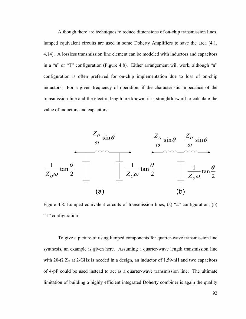
92
Although there are techniques to reduce dimensions of on-chip transmission lines,
lumped equivalent circuits are used in some Doherty Amplifiers to save die area [4.1,
4.14]. A lossless transmission line element can be modeled with inductors and capacitors
in a “π” or “T” configuration (Figure 4.8). Either arrangement will work, although “π”
configuration is often preferred for on-chip implementation due to loss of on-chip
inductors. For a given frequency of operation, if the characteristic impedance of the
transmission line and the electric length are known, it is straightforward to calculate the
value of inductors and capacitors.
θω
sinOZ
2tan1 θ
ωOZ
θω
sinOZθ
ωsinOZ
2tan1 θ
ωOZ 2tan1 θ
ωOZ
Figure 4.8: Lumped equivalent circuits of transmission lines, (a) “π” configuration; (b)
“T” configuration
To give a picture of using lumped components for quarter-wave transmission line
synthesis, an example is given here. Assuming a quarter-wave length transmission line
with 20-Ω ZO at 2-GHz is needed in a design, an inductor of 1.59-nH and two capacitors
of 4-pF could be used instead to act as a quarter-wave transmission line. The ultimate
limitation of building a highly efficient integrated Doherty combiner is again the quality

93
factor of on-chip passives, especially inductors. Another issue with this approach is the
inherent narrow bandwidth.
4.2.2.2 Wilkinson Power Combiner
In the RF/microwave community, the importance of Wilkinson power combiner is
equivalent to that of Widlar current source in the analog community. It was invented
around 1960, relying on quarter-wave transmission lines to match the split ports to the
common port [4.15]. Figure 4.9(a) shows a 2-way Wilkinson power combiner. In the
context of power amplifiers design, matching every port is not necessary at all. In fact,
conjugate match should be avoided in almost every case for better performance. Since
there are many excellent text books, for example [4.16, 4.17], covering Wilkinson power
combiner extensively, it will not be analyzed in detail here. One note, however, should
be pointed out here. When in-phase outputs are combined, there is no power dissipated in
the isolation resistor. It is 100% efficient just like an ideal Wilkinson power splitter.
Lumped components can be synthesized to implement a Wilkinson power combiner
(Figure 4.9(b)).
(a)
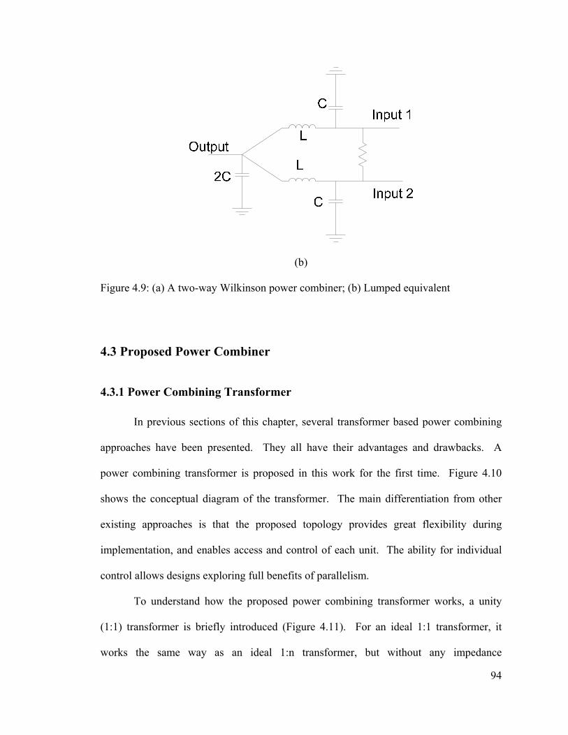
94
(b)
Figure 4.9: (a) A two-way Wilkinson power combiner; (b) Lumped equivalent
4.3 Proposed Power Combiner
4.3.1 Power Combining Transformer
In previous sections of this chapter, several transformer based power combining
approaches have been presented. They all have their advantages and drawbacks. A
power combining transformer is proposed in this work for the first time. Figure 4.10
shows the conceptual diagram of the transformer. The main differentiation from other
existing approaches is that the proposed topology provides great flexibility during
implementation, and enables access and control of each unit. The ability for individual
control allows designs exploring full benefits of parallelism.
To understand how the proposed power combining transformer works, a unity
(1:1) transformer is briefly introduced (Figure 4.11). For an ideal 1:1 transformer, it
works the same way as an ideal 1:n transformer, but without any impedance
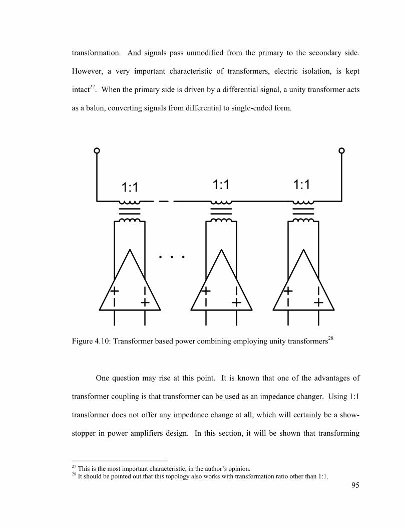
95
transformation. And signals pass unmodified from the primary to the secondary side.
However, a very important characteristic of transformers, electric isolation, is kept
intact27. When the primary side is driven by a differential signal, a unity transformer acts
as a balun, converting signals from differential to single-ended form.
1:1 1:1 1:1
Figure 4.10: Transformer based power combining employing unity transformers28
One question may rise at this point. It is known that one of the advantages of
transformer coupling is that transformer can be used as an impedance changer. Using 1:1
transformer does not offer any impedance change at all, which will certainly be a show-
stopper in power amplifiers design. In this section, it will be shown that transforming
27 This is the most important characteristic, in the author’s opinion. 28 It should be pointed out that this topology also works with transformation ratio other than 1:1.

96
impedance could still be achieved by connecting several 1:1 transformers together. And
in the next chapter, it will be explained why 1:1 transformer is preferred as building
blocks when implementing power combining transformer on silicon.
Figure 4.11: An ideal unity transformer
To obtain any impedance transformation, more than one unity transformer is
needed. A four-unit power combining transformer is shown in Figure 4.12 as an example.
The primary sides of four independent unity transformers are driven by four independent,
nonetheless synchronized sources with the same signal level in parallel. The secondary
sides of four independent unity transformers are stacked together in series. Assuming
signal levels are equal on the primary sides, that is:
iVVVVV ==== 4321
Because the secondary sides are connected in series, the “ac ground” of the secondary
side of each unity transformer is lifted so that the ac voltages add on the secondary:
iL VVVVVV 44321 =+++=
For current, since the secondary sides are connected in series, it forces the currents in the
primary sides equal to each other:
LIIIII ==== 4321

97
Figure 4.12: A four-way power combining transformer composed of 4 unity transformers
The impedance seen from the primary side of each unity transformer can be derived:
LL
L RIV
IVZZZZ
41
41
1
14321 ======
The power delivered to the load is:
L
i
L
i
L
LL R
VRV
RVP
222
8)4(
21
21
===
And the power from each source is:

98
L
i
L
ii
RV
R
VZV
PPPP22
1
2
4321 2
412
121
======
Therefore, it is obvious that power is combined from each unity transformer and
delivered to the load:
4321 PPPPPL +++=
Several important characteristics of the power combining transformer with N
unity transformers are summarized here:
a. Power generated from primary sides are picked up by the secondary side and then
combined through magnetic coupling. The combining ratio is N.
b. The ac voltages at the secondary sides add to achieve enough voltage swing. Due
to electronic isolation of the transformer, the primary sides still work with low
voltage, away from breakdown region. The voltage ratio between the swing at the
load and the swing at one of the primaries is N.
c. Contrarily, the current on both sides of the transformer equal to each other. The
ratio of total currents between the two sides is 1/N. And the current ratio of
current in the secondary sides to that of one of the primaries is obviously 129.
d. The impedance seen by each port at the primary sides is N times smaller than the
load at the secondary. The impedance transformation ratio is N.
Several advantages and potential applications offered by this power combining
transformer are presented, benefited from parallelism using power combining transformer.
4.3.1.1 Noise
29 This is an important feature in practice since it effectively reduces loss caused by parasitics. This will be examined later in detail.

99
It may seem irrelevant here to talk about noise in PAs. This impression is
certainly invalid in a full duplex system. Due to finite rejection provided by duplex filter,
excessive noise from the power amplifier will reduce the receiver sensitivity. Even worse,
the disturbance might be dependent on the input signal level at the receiver input, which
further complicates the system design. Considering an N-way power combining PA with
N identical amplifiers, an equivalent model (Figure 4.13) is used to study signal and noise
relationship between input and output.
Figure 4.13: An equivalent model for an N-way power combining PA with additive
noise30
Noise in the combining PA can be divided into the following categories:
30 Signals are represented in voltage domain in the context of integrated circuit design

100
a. Correlated noise from a source common to all the individual amplifiers, including
thermal noise, amplitude modulation (AM) and phase modulation (PM) noise
generated by circuits preceding PAs.
b. Uncorrelated thermal noise generated in the individual amplifiers.
c. Uncorrelated AM noise and PM noise generated by individual amplifiers as a
result of the up-conversion of low frequency noise. Such noise is generally
characterized by a 1/f noise spectrum.
Since AM noise and PM noise are up-converted 1/f noise, and will have exactly
the same characteristics as thermal noise, the following derivations will only have
thermal noise (Figure 4.14) in expressions to avoid lengthy equations.
Because the signals will be added in amplitude, the output voltage is:
isANos __ ⋅⋅=
The input signal has noise common to all individual amplifiers, therefore this noise will
be added up in amplitude at the output. The noise generated by each branch is, however,
uncorrelated. The total output noise power is:
222 )_()_(_ thnANinANon ⋅⋅+⋅⋅=
Then SNR at the output is:
22
2
2
2
_1_
___
thnN
in
isonosSNRoutput
+==
Depending on the input noise level, the improvement to the SNR of an individual
branch could be as high as N. Assuming that input signal level, input noise level, input
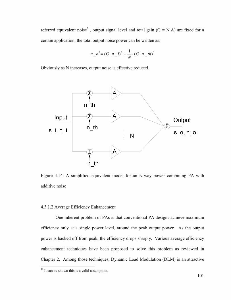
101
referred equivalent noise31, output signal level and total gain (G = N·A) are fixed for a
certain application, the total output noise power can be written as:
222 )_(1)_(_ thnGN
inGon ⋅⋅+⋅=
Obviously as N increases, output noise is effective reduced.
Figure 4.14: A simplified equivalent model for an N-way power combining PA with
additive noise
4.3.1.2 Average Efficiency Enhancement
One inherent problem of PAs is that conventional PA designs achieve maximum
efficiency only at a single power level, around the peak output power. As the output
power is backed off from peak, the efficiency drops sharply. Various average efficiency
enhancement techniques have been proposed to solve this problem as reviewed in
Chapter 2. Among those techniques, Dynamic Load Modulation (DLM) is an attractive 31 It can be shown this is a valid assumption.

102
approach32 . The power combining transformer proposed in this work has a useful
property to modulate the load seen by individual amplifiers on the primary sides. Two
types of load modulation could be implemented, namely digital and analog load
modulation33. Here, digital control is introduced because of its simplicity, with a four-
way (N=4) power combined amplifier as an example. Each amplifier acts as a current
source with transconductance gm. Maximum swing is Vo at the output of each amplifier,
when input swing is Vi. At primaries, amplifiers are equally weighted. Individual
amplifiers at the primaries will be turned on or off as required output power varies,
controlled by a thermometric input code (Figure 4.15).
Full power: At the peak power, every individual amplifier is on. Now the load seen by
each amplifier is:
LRR41
=
The efficiency of each amplifier, as well as the efficiency of power combined amplifier,
reaches maximum.
maxηηη == unitoverall
Voltage gain of each amplifier is:
LRgmA41⋅=
Total gain of power combining amplifier is:
LRgmANGainV ⋅=⋅=_
And the peak RF output power is:
32 The Doherty Amplifier is an example. 33 Analog load modulation is similar to Doherty technique.
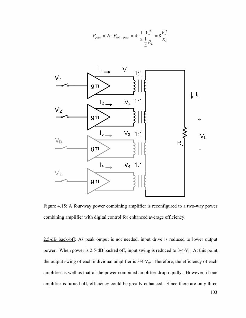
103
L
o
L
opeakunitpeak R
V
R
VPNP
22
_ 8
412
14 =⋅=⋅=
Figure 4.15: A four-way power combining amplifier is reconfigured to a two-way power
combining amplifier with digital control for enhanced average efficiency.
2.5-dB back-off: As peak output is not needed, input drive is reduced to lower output
power. When power is 2.5-dB backed off, input swing is reduced to 3/4·Vi. At this point,
the output swing of each individual amplifier is 3/4·Vo. Therefore, the efficiency of each
amplifier as well as that of the power combined amplifier drop rapidly. However, if one
amplifier is turned off, efficiency could be greatly enhanced. Since there are only three

104
amplifiers (N=3) contributing to the output, a four-way power combined amplifier is
reconfigured to a three-way power combined amplifier. The load seen by each active
amplifier is now:
LRR31
=
Voltage gain of each amplifier becomes:
LRgmA31⋅=
The output swing of each active amplifier returns to the maximum value:
oiLinputoutput VVRgmVAV =⋅⋅=⋅=43
31
So do the efficiency of individual amplifiers and that of the power combined amplifier:
maxηηη == unitoverall
Total gain of power combining amplifier is:
LRgmANGainV ⋅=⋅=_
And the RF output power at this point is:
peakL
o
L
ounitout P
RV
R
VPNP
169
29
312
1322
==⋅=⋅=
6-dB back-off: If the input is further reduced to 1/2·Vi, one more individual amplifier
could be turned off to improve efficiency at back-off. Now a four-way power combined
amplifier is reconfigured to a two-way (N=2) power combined amplifier. The load seen
by each active amplifier is now:
LRR21
=

105
Voltage gain of each amplifier becomes:
LRgmA21⋅=
The output swing of each active amplifier returns to the maximum value:
oiLinputoutput VVRgmVAV =⋅⋅=⋅=21
21
So do the efficiency of individual amplifiers and that of the power combined amplifier:
maxηηη == unitoverall
Total gain of power combining amplifier is:
LRgmANGainV ⋅=⋅=_
And the RF output power at this point is:
peakL
o
L
ounitout P
RV
R
VPNP
412
212
1222
==⋅=⋅=
12-dB back-off: As the input is reduced to 1/4·Vi at 12-dB back-off, only one amplifier
need to be on (N=1). The load seen by each active amplifier is just the load itself without
any impedance transformation:
LRR =
Voltage gain of each amplifier becomes:
LRgmA ⋅=
The output swing of each active amplifier returns to the maximum value:
oiLinputoutput VVRgmVAV =⋅⋅=⋅=41
So does the efficiency of the individual amplifier and that of the power combined
amplifier:

106
maxηηη == unitoverall
Total gain of power combining amplifier is:
LRgmANGainV ⋅=⋅=_
And the RF output power at this point is:
peakL
o
L
ounitout P
RV
RV
PNP161
21
211
22
==⋅=⋅=
It should be pointed out that voltage gain is constant as output power is backed off
from peak, which is a desirable feature for system design. Figure 4.16 illustrates the
efficiency of a four-way ideal transformer combined power amplifier with digital
control.34
Output Power
Effi
cien
cy
Conventional PA
Proposed PA
Output Power
Effi
cien
cy
Conventional PA
Proposed PA
Figure 4.16: A comparison of efficiency between the PA based on proposed power
combining transformer and the conventional PA
34 If unit amplifier is class-A, the efficiency of unit amplifier degrades at power back-off. However, the overall power amplifier efficiency is still improved. Class A PA is rarely seen in practice. Most linear PAs are class-AB or class B.
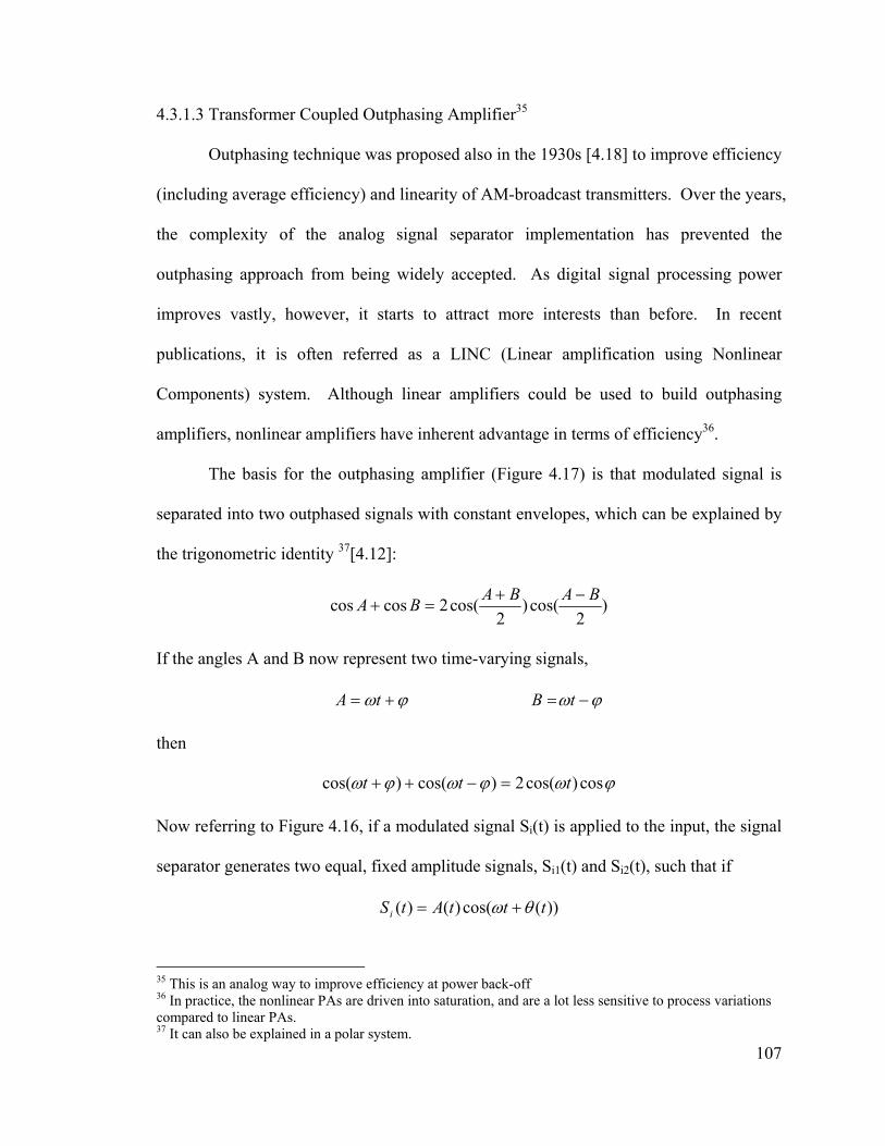
107
4.3.1.3 Transformer Coupled Outphasing Amplifier35
Outphasing technique was proposed also in the 1930s [4.18] to improve efficiency
(including average efficiency) and linearity of AM-broadcast transmitters. Over the years,
the complexity of the analog signal separator implementation has prevented the
outphasing approach from being widely accepted. As digital signal processing power
improves vastly, however, it starts to attract more interests than before. In recent
publications, it is often referred as a LINC (Linear amplification using Nonlinear
Components) system. Although linear amplifiers could be used to build outphasing
amplifiers, nonlinear amplifiers have inherent advantage in terms of efficiency36.
The basis for the outphasing amplifier (Figure 4.17) is that modulated signal is
separated into two outphased signals with constant envelopes, which can be explained by
the trigonometric identity 37[4.12]:
)2
cos()2
cos(2coscos BABABA −+=+
If the angles A and B now represent two time-varying signals,
ϕωϕω −=+= tBtA
then
ϕωϕωϕω cos)cos(2)cos()cos( ttt =−++
Now referring to Figure 4.16, if a modulated signal Si(t) is applied to the input, the signal
separator generates two equal, fixed amplitude signals, Si1(t) and Si2(t), such that if
))(cos()()( tttAtSi θω +=
35 This is an analog way to improve efficiency at power back-off 36 In practice, the nonlinear PAs are driven into saturation, and are a lot less sensitive to process variations compared to linear PAs. 37 It can also be explained in a polar system.
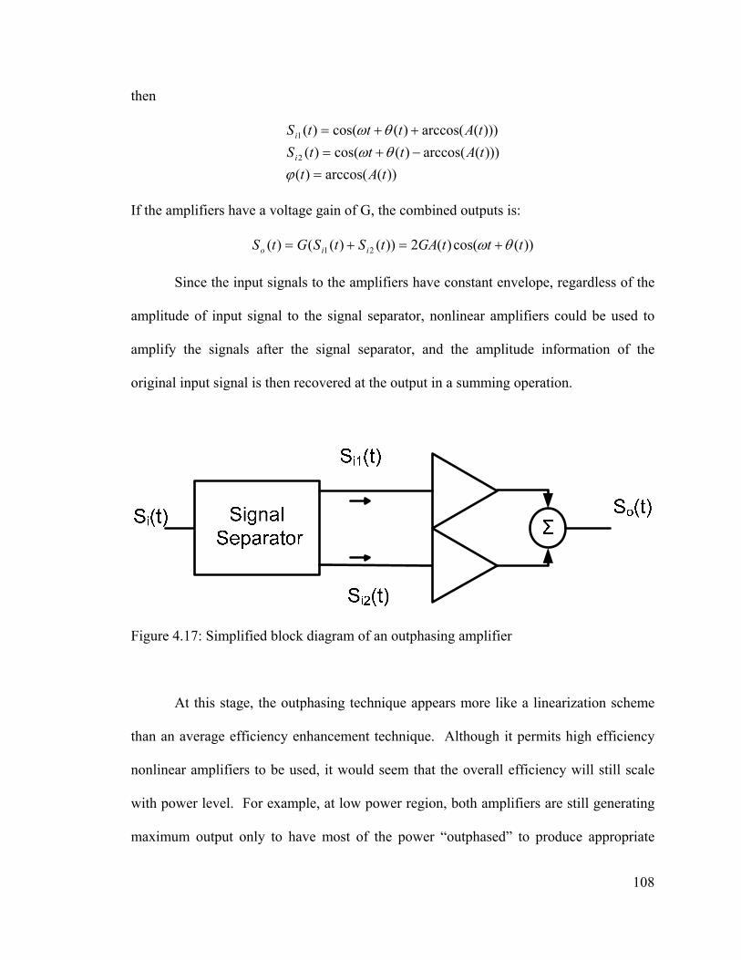
108
then
))(arccos()()))(arccos()(cos()()))(arccos()(cos()(
2
1
tAttAtttStAtttS
i
i
=−+=++=
ϕθωθω
If the amplifiers have a voltage gain of G, the combined outputs is:
))(cos()(2))()(()( 21 tttGAtStSGtS iio θω +=+=
Since the input signals to the amplifiers have constant envelope, regardless of the
amplitude of input signal to the signal separator, nonlinear amplifiers could be used to
amplify the signals after the signal separator, and the amplitude information of the
original input signal is then recovered at the output in a summing operation.
Figure 4.17: Simplified block diagram of an outphasing amplifier
At this stage, the outphasing technique appears more like a linearization scheme
than an average efficiency enhancement technique. Although it permits high efficiency
nonlinear amplifiers to be used, it would seem that the overall efficiency will still scale
with power level. For example, at low power region, both amplifiers are still generating
maximum output only to have most of the power “outphased” to produce appropriate
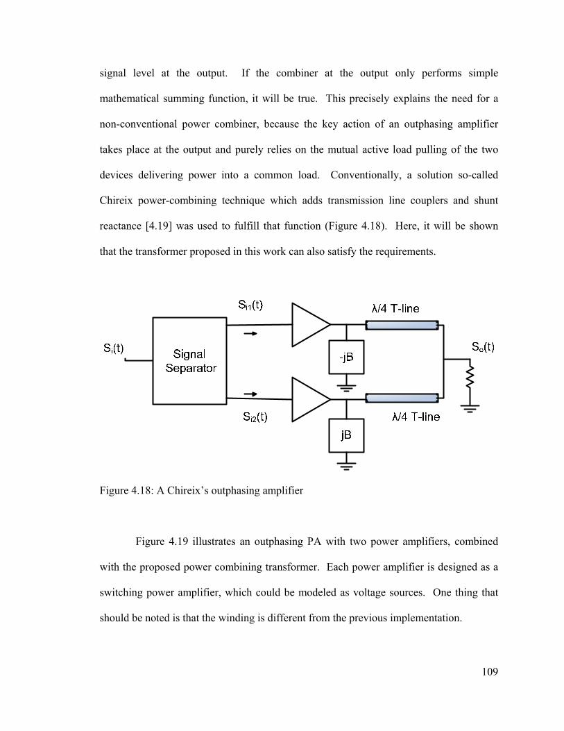
109
signal level at the output. If the combiner at the output only performs simple
mathematical summing function, it will be true. This precisely explains the need for a
non-conventional power combiner, because the key action of an outphasing amplifier
takes place at the output and purely relies on the mutual active load pulling of the two
devices delivering power into a common load. Conventionally, a solution so-called
Chireix power-combining technique which adds transmission line couplers and shunt
reactance [4.19] was used to fulfill that function (Figure 4.18). Here, it will be shown
that the transformer proposed in this work can also satisfy the requirements.
Figure 4.18: A Chireix’s outphasing amplifier
Figure 4.19 illustrates an outphasing PA with two power amplifiers, combined
with the proposed power combining transformer. Each power amplifier is designed as a
switching power amplifier, which could be modeled as voltage sources. One thing that
should be noted is that the winding is different from the previous implementation.

110
The signal separator circuits generate two sinewave signals with phases of φ and –
φ. These two signals are then amplified by the nonlinear power amplifiers and added
together to produce the output signal. The outputs of the two power amplifiers (Figure
4.20) can be written in phasor form38 as:
)sin(cos)sin(cos
2
1
ϕϕϕϕ
jVVjVV
−=+=
The output across the load RL is:
ϕsin221 VjVVVL =−=
so that the output voltage after summing is proportional to sinφ. If the input signal
separator generates a phase shift such that
))(arcsin( tA=ϕ
then the output voltage at the load resistor fully recovers of the original AM signal.
When φ = 90°, two output voltages combine, resulting maximum amplitude. When φ =
0°, zero amplitude is achieved.
Referring to Figure 4.19 (b), the current at the load, IL, is given as:
LL
LL R
VVRVI 21 −==
Therefore, the effective load seen by the two RF voltage generators V1 and V2 are:
)cot1(2sin2
sincos
)cot1(2sin2
sincos
21
22
21
11
ϕϕ
ϕϕ
ϕϕ
ϕϕ
jR
Rj
jRVV
VZ
jRRj
jRVV
VZ
LLL
LLL
+=−
−=−
−=
−=+
=−
=
38 The math will be easy to digest using phasor form because it is more intuitive.

111
Figure 4.19: (a) An outphasing amplifier with the proposed power combiner; (b) An
equivalent model of the outphasing amplifier
To further understand active load pulling effect, RF load seen by the RF generator
V1 is shown in Figure 4.21 (a), a resistive component in series with a reactive component.
The same kind of load modulation is also seen by V2 (Figure 4.22). The reactive
component is caused by signal separator operation which generates the phase difference
between two signal paths, and the reactance is a function of the phase modulation φ. A
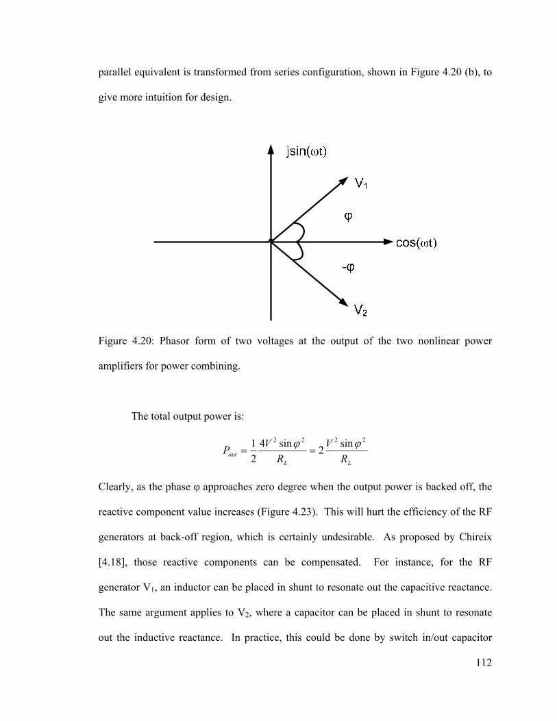
112
parallel equivalent is transformed from series configuration, shown in Figure 4.20 (b), to
give more intuition for design.
Figure 4.20: Phasor form of two voltages at the output of the two nonlinear power
amplifiers for power combining.
The total output power is:
LLout R
VR
VP2222 sin2sin4
21 ϕϕ
==
Clearly, as the phase φ approaches zero degree when the output power is backed off, the
reactive component value increases (Figure 4.23). This will hurt the efficiency of the RF
generators at back-off region, which is certainly undesirable. As proposed by Chireix
[4.18], those reactive components can be compensated. For instance, for the RF
generator V1, an inductor can be placed in shunt to resonate out the capacitive reactance.
The same argument applies to V2, where a capacitor can be placed in shunt to resonate
out the inductive reactance. In practice, this could be done by switch in/out capacitor

113
bank. Although the magnitude of the compensating reactance will vary with phase
modulation φ, this could be solved by switching capacitors as well.
One observation is that to deal with power back-off more than 20dB, phase
modulation resolution down to several degrees is required. This is certainly achievable
with today’s DSP advances.
2sin1
2 ϕ⋅= LR
R
2LRR =
2cot LRjjx ⋅−= ϕ
LRjjx ⋅−=)2sin(
1ϕ
Figure 4.21: (a) RF load seen by the RF generator V1; (b) A parallel equivalent model
2sin1
2 ϕ⋅= LR
R2
LRR =
2cot LR
jjx ⋅= ϕLRjjx ⋅=
)2sin(1ϕ
Figure 4.22: (a) RF load seen by the RF generator V2; (b) A parallel equivalent model
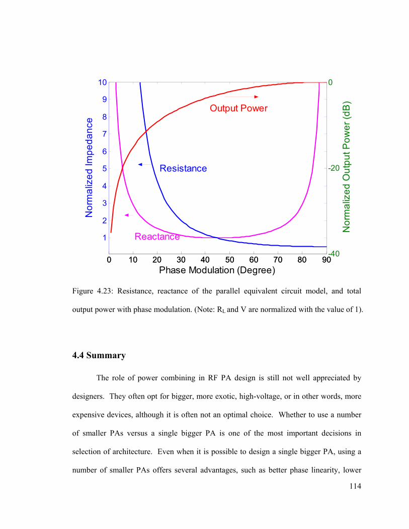
114
0 10 20 30 40 50 60 70 80 90
1
2
3
4
5
6
7
8
9
10N
orm
aliz
ed Im
peda
nce
0 10 20 30 40 50 60 70 80 90-40
-20
0
Phase Modulation (Degree)
Nor
mal
ized
Out
put P
ower
(dB
)
Output Power
Resistance
Reactance
Figure 4.23: Resistance, reactance of the parallel equivalent circuit model, and total
output power with phase modulation. (Note: RL and V are normalized with the value of 1).
4.4 Summary
The role of power combining in RF PA design is still not well appreciated by
designers. They often opt for bigger, more exotic, high-voltage, or in other words, more
expensive devices, although it is often not an optimal choice. Whether to use a number
of smaller PAs versus a single bigger PA is one of the most important decisions in
selection of architecture. Even when it is possible to design a single bigger PA, using a
number of smaller PAs offers several advantages, such as better phase linearity, lower

115
chip temperature, and less heat removal requirements. When the required output power
cannot be achieved by a single transistor, power combining is necessary to generate the
required power from several units.
4.5 References
[4.1] N. Wongkomet, L. Tee and P. Gray, “A 1.7GHz 1.5W CMOS RF Doherty Power
Amplifier for Wireless Communications”, IEEE ISSCC Digest of Technical Papers, pp.
486-487, February 2006
[4.2] T. Sowlati, D.M.W. Leenaerts, “A 2.4-GHz 0.18-µm CMOS self-biased cascode
power amplifier”, IEEE J. Solid-State Circuits, vol. 38, no. 8, pp. 1318-1324, August,
2003
[4.3] C.R. Battjes, “A wide-band high-voltage monolithic amplifier”, IEEE J. Solid-State
Circuits, vol. sc-8, no. 6, pp. 408-413, December, 1973
[4.4] J.G. McRory, G.G. Rabjohn, R.H. Johnston, “Transformer coupled stacked FET
power amplifiers”, IEEE J. Solid-State Circuits, vol. 34, no. 2, pp. 157-161, February,
1999
[4.5] E.F. Sartori, “Hybrid Transformers”, IEEE Trans. on Parts, Materials, and
Packaging, PMP-4, pp.59-66, September, 1968
[4.6] I. Aoki, S. Kee, D. B. Rutledge and A. Hajimiri, “Fully integrated CMOS power
amplifier design using the Distributive Active-Transformer architecture”, IEEE J. Solid-
State Circuits, vol. 37, no. 3, pp. 371-383, March, 2002.

116
[4.7] S. Kim, K. Lee, J. Lee, B. Kim, S.D. Kee, I.Aoki, D.B. Rutledge, “An optimized
design of distributed active transformer”, IEEE Trans. Microwave Theory Tech., vol. 53,
no. 1, pp. 380-388, January, 2005
[4.8] T.S.D. Cheung, J.R.Long, Y.V. Tretiakov, D.L. Harame, “A 21-27GHz self-
shielded 4-way power-combining PA balun”, Proc. of Custom Integrated Circuits
Conference, pp.617-620, 2004
[4.9] A. Vasylyev, P. Weger, W. Bakalski, W. Simburger, “Fully-integrated 32dBm, 1.5-
2.9GHz SiGe-bipolar power amplifier using power-combining transformer”, IEEE Elec.
Lett., vol. 41, no. 16, pp. 35-36, August, 2005
[4.10] S. Seki, H.Hasegawa, “Cross-tie slow-wave coplanar waveguide on semi-
insulating GaAs substrates”, IEEE Elec. Lett., vol. 17, no. 25, pp. 940-941, December,
1981
[4.11] W. H. Doherty, “A new high efficiency power amplifier for modulated waves”, in
Proc. IRE, vol. 24, pp. 1163-1182, September 1936
[4.12] Steve C. Cripps, “RF Power Amplifiers for Wireless Communications”, Artech
House, 1999.
[4.13] P.B. Kenington, “High-Linearity RF Amplifier Design,” Artech House Inc.,2000.
[4.14] C. Tongchoi, M. Chongcheawchamnan, A. Worapishet, “Lumped element based
Doherty power amplifier topology in CMOS process”, Proc. of ISCAS, vol. 1, pp. 25-28,
2003
[4.15] E. Wilkinson, “An N-way hybrid power divider”, IRE Trans. on Microwave
Theory and Techniques, vol. MTT-8, pp. 116-118, January, 1960

117
[4.16] R. E. Collin, “Foundations for Microwave Engineering”, Second Edition, IEEE
Press, N.Y. 2001
[4.17] D. M. Pozar, “Microwave Engineering”, Third Edition, John Wiley & Sons, Inc.,
N.J. 2005.
[4.18] H. Chireix, “High power outphasing modulation”, Proc. IRE, vol. 23, no. 11, pp.
1370-1392, November 1935
[4.19] F.H. Raab, “Efficiency of outphasing RF power amplifier systems”, IEEE Trans,
commun., vol. 33, no. 10, pp. 1094-1099, October 1985

118
Chapter 5. The Power Combining Transformer Design
5.1 Impedance transformation
5.2 Design considerations of transformers for power amplifiers
5.3 Design and Implementation of the proposed transformer
5.4 Discussions and Summary
5.5 References
The power combining transformer proposed in this work is absolutely important
in order to achieve highly efficient power amplifiers. In this chapter, LC resonant
matching networks are compared to transformer matching, which explains why
transformer matching is desired when impedance transformation ratio is high. Practical
issues in designing low impedance inductors and highly efficient transformers will be
considered next. The various topologies of on-chip transformer are studied. Based on
those considerations, the topology of the proposed power combining transformer is
introduced. At last, some design guidelines will be given.
5.1 Impedance Transformation
The importance of impedance transformation needs no more introduction. In the
context of power amplifier design, it is necessary to transform the load of a power
amplifier to a value which is a function of the supply voltage and the required power39.
Because lossless reactive components do not exist, all impedance matching networks will 39 It is well known that maximum power is transferred under conjugate matched condition. Besides it may not be realizable, the efficiency under this case is only 50%. Therefore, in power amplifiers design, the output is rarely conjugate matched.
119
have some insertion loss. These losses can be quite pronounced in PA circuits which
degrade the efficiency directly. This issue is even serious when designing PA with state-
of-the-art CMOS technologies, because of required high impedance transformation ratio
and lossy on-chip passive components40. Three networks are often used in practice for
impedance transformation: LC resonant matching networks and transformer matching
networks, both lumped networks, and distributive networks with transmission lines. The
analyses on those networks have been well documented. Interested readers should refer
to the literature [5.1-5.3] to probe further. LC resonant matching networks and
transformer matching networks are briefly discussed in this section. Similar analyses can
be found in [5.4].
5.1.1 LC Resonant Matching Network
LC resonant matching is straightforward to implement. A single stage “L-match”
is shown in Figure 5.1, composed of a capacitor and an inductor41. A lossy inductor can
be analyzed with series equivalent circuits or parallel equivalent circuits by adding a
resistor to model the loss (Figure 5.2), where
)1(
)1(
2
2
2
L
Lsp
Lsp
p
p
s
sL
QQLL
QRR
LR
RLQ
+=
+=
==ω
ω
40 Since on-chip capacitors Q is usually higher than inductors, only inductor loss is considered here for simplicity. This is especially true for low GHz range, which is the focus of this work. 41 Both topologies can transform the load impedance to a lower value. With series capacitor approach, it will block DC current flowing into the load. With parallel capacitor approach, it will short high order harmonics automatically due to its low pass nature.
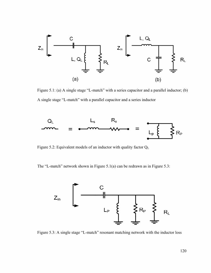
120
Figure 5.1: (a) A single stage “L-match” with a series capacitor and a parallel inductor; (b)
A single stage “L-match” with a parallel capacitor and a series inductor
Figure 5.2: Equivalent models of an inductor with quality factor QL
The “L-match” network shown in Figure 5.1(a) can be redrawn as in Figure 5.3:
Figure 5.3: A single stage “L-match” resonant matching network with the inductor loss
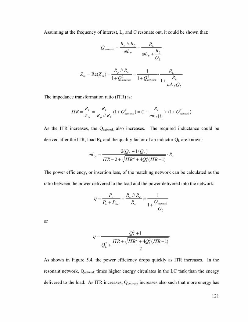
121
Assuming at the frequency of interest, Lp and C resonate out, it could be shown that:
L
Lp
L
P
Lpnetwork
QRL
RL
RRQ
+==ωω
//
LP
L
L
networknetwork
Lpinin
QLR
RQQ
RRZZ
ω+
⋅+
=+
==11
11
//)Re( 22
The impedance transformation ratio (ITR) is:
)1()1()1(//
22network
LP
Lnetwork
Lp
L
in
L QQL
RQRR
RZRITR +⋅+=+==
ω
As the ITR increases, the Qnetwork also increases. The required inductance could be
derived after the ITR, load RL and the quality factor of an inductor QL are known:
L
L
LLp R
ITRQITRITR
QQL ⋅−++−
+=
)1(42
)/1(222
ω
The power efficiency, or insertion loss, of the matching network can be calculated as the
ratio between the power delivered to the load and the power delivered into the network:
L
networkL
PL
dissL
L
QQR
RRPP
P
+≈=
+=
1
1//η
or
2)1(4
122
2
2
−+++
+=
ITRQITRITRQ
Q
LL
Lη
As shown in Figure 5.4, the power efficiency drops quickly as ITR increases. In the
resonant network, Qnetwork times higher energy circulates in the LC tank than the energy
delivered to the load. As ITR increases, Qnetwork increases also such that more energy has
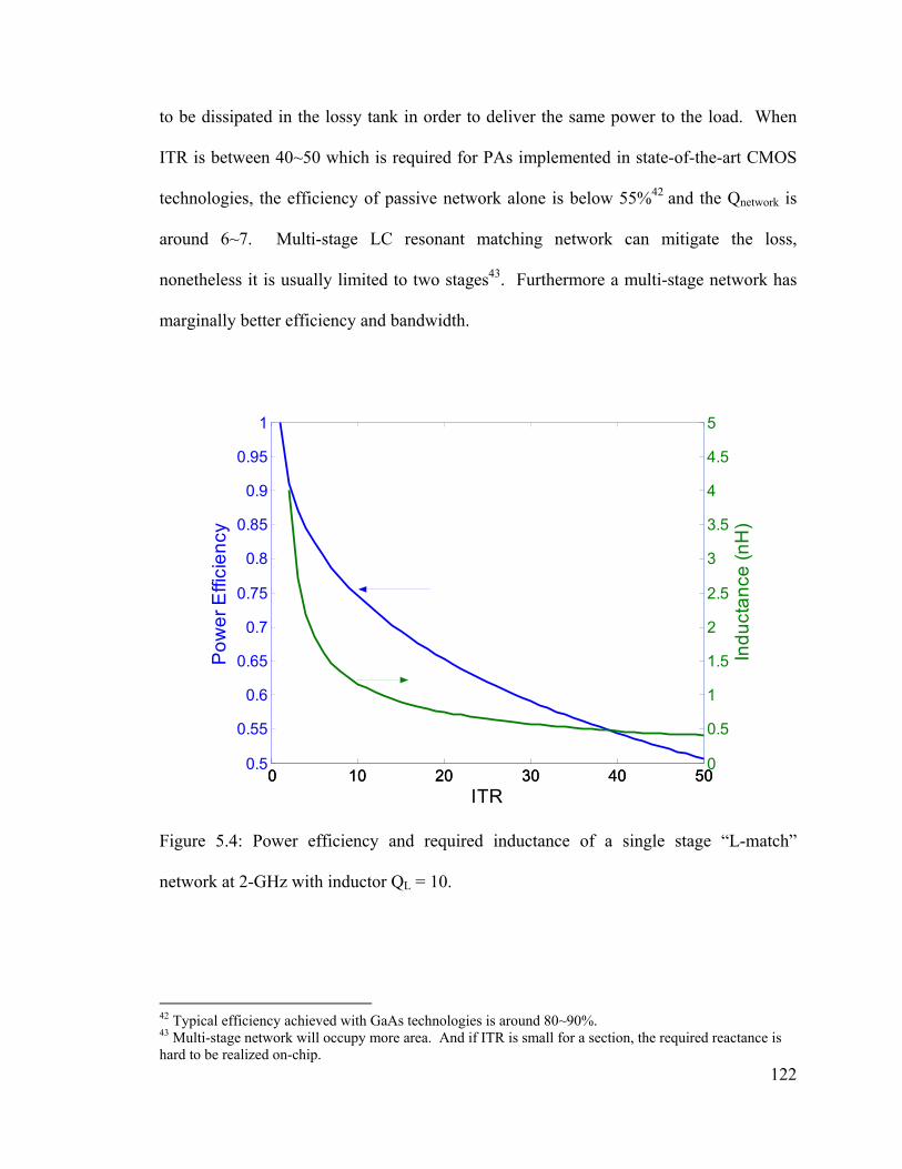
122
to be dissipated in the lossy tank in order to deliver the same power to the load. When
ITR is between 40~50 which is required for PAs implemented in state-of-the-art CMOS
technologies, the efficiency of passive network alone is below 55%42 and the Qnetwork is
around 6~7. Multi-stage LC resonant matching network can mitigate the loss,
nonetheless it is usually limited to two stages43. Furthermore a multi-stage network has
marginally better efficiency and bandwidth.
0 10 20 30 40 500.5
0.55
0.6
0.65
0.7
0.75
0.8
0.85
0.9
0.95
1
Pow
er E
ffici
ency
0 10 20 30 40 500
0.5
1
1.5
2
2.5
3
3.5
4
4.5
5
ITR
Indu
ctan
ce (n
H)
Figure 5.4: Power efficiency and required inductance of a single stage “L-match”
network at 2-GHz with inductor QL = 10.
42 Typical efficiency achieved with GaAs technologies is around 80~90%. 43 Multi-stage network will occupy more area. And if ITR is small for a section, the required reactance is hard to be realized on-chip.
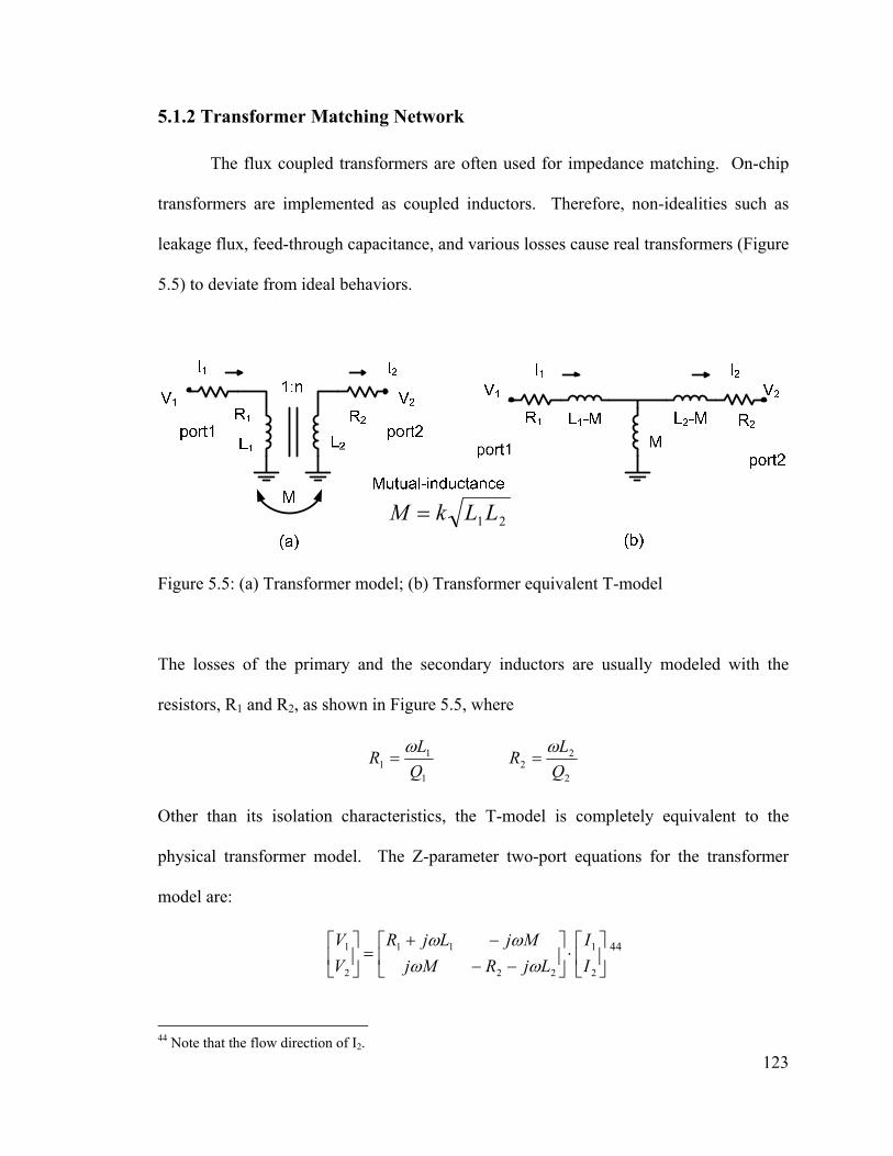
123
5.1.2 Transformer Matching Network
The flux coupled transformers are often used for impedance matching. On-chip
transformers are implemented as coupled inductors. Therefore, non-idealities such as
leakage flux, feed-through capacitance, and various losses cause real transformers (Figure
5.5) to deviate from ideal behaviors.
21LLkM =
Figure 5.5: (a) Transformer model; (b) Transformer equivalent T-model
The losses of the primary and the secondary inductors are usually modeled with the
resistors, R1 and R2, as shown in Figure 5.5, where
2
22
1
11 Q
LRQLR ωω
==
Other than its isolation characteristics, the T-model is completely equivalent to the
physical transformer model. The Z-parameter two-port equations for the transformer
model are:
⋅
−−
−+=
2
1
22
11
2
1
II
LjRMjMjLjR
VV
ωωωω 44
44 Note that the flow direction of I2.

124
The T-model can be modified so it is expressed in terms of leakage inductance and
magnetizing inductance, which circuit designers are more familiar with than self-
inductance and mutual-inductance (Figure 5.6). The magnetizing and leakage inductance
are:
1111 )1( LkLkLL Lm −==
2222 )1( LkLkLL Lm −==
Now, let’s define the effective turn ratio,
nkLL
LL
LL
l
l
m
m ⋅====1
2
1
2
1
2α
so the mutual inductance can be expressed as:
2121211
mmmm LLLLLLkMα
α ====
The Z-parameter two port equations become:
)()( 2111111 IILjILjRV ml αωω −++=
2222112 )()( ILjRIILjV lm ωααω +−−=
Given a load connected to port 2 (Figure 5.7), the power efficiency of the transformer is:
21
2221
222
12
2 )())/(1/)1(()/(
)/(Lk
CLkLkRRRRR
R
eqeqeq
eq
ωωαωωα
αη
−−+++++
=
where
222
22
2 ])(1[CR
CRCL
Leq ω
ωα +=
22
2
)(1/
CRRR
L
Leq ω
α+
=
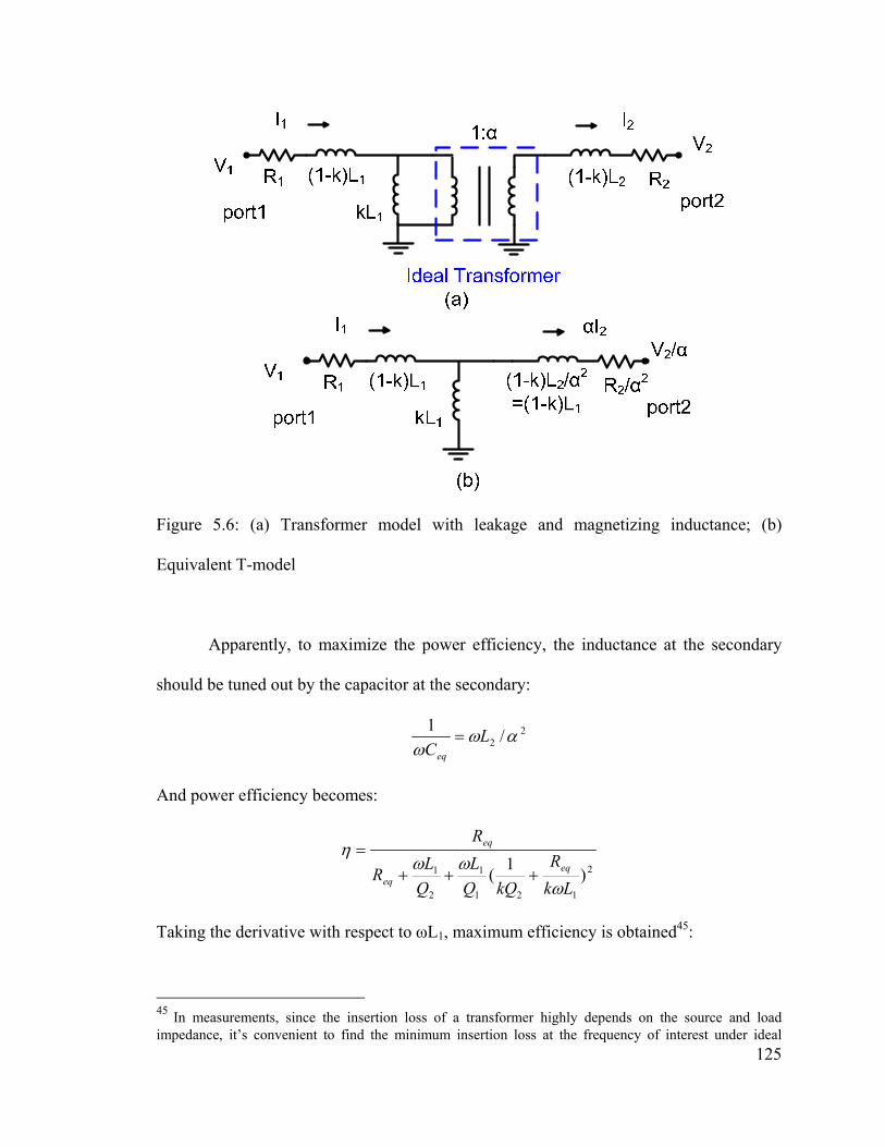
125
Figure 5.6: (a) Transformer model with leakage and magnetizing inductance; (b)
Equivalent T-model
Apparently, to maximize the power efficiency, the inductance at the secondary
should be tuned out by the capacitor at the secondary:
22 /1 αω
ωL
Ceq
=
And power efficiency becomes:
2
121
1
2
1 )1(Lk
RkQQ
LQLR
R
eqeq
eq
ωωω
η+++
=
Taking the derivative with respect to ωL1, maximum efficiency is obtained45:
45 In measurements, since the insertion loss of a transformer highly depends on the source and load impedance, it’s convenient to find the minimum insertion loss at the frequency of interest under ideal

126
)11(1221
1
221
221
221
max
kQQkQQkQQ+++
=η
when
221 1 αω loadR
AAL ⋅+
= (2
2
122
11
kQQ
Q
A+
= )
To complete the design, C2 need to be sized accordingly:
AR
CL=
2
1ω
Figure 5.7: (a) Transformer equivalent T-model with a load resistor and tuning
capacitor46; (b) Transformer T-model after parallel to series conversion at the load
conditions, a bi-conjugate source and load match, using s-parameters to get Gmax. Alternatively, GP can be calculated based on S-parameters to derive insertion loss. 46 The tuning capacitor could be placed in series with the load. However, in PA design, parallel placement is preferred since it will transform the load to a lower value.
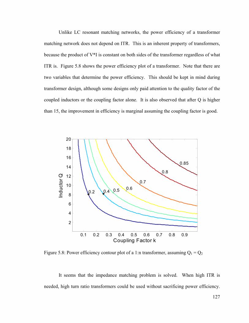
127
Unlike LC resonant matching networks, the power efficiency of a transformer
matching network does not depend on ITR. This is an inherent property of transformers,
because the product of V*I is constant on both sides of the transformer regardless of what
ITR is. Figure 5.8 shows the power efficiency plot of a transformer. Note that there are
two variables that determine the power efficiency. This should be kept in mind during
transformer design, although some designs only paid attention to the quality factor of the
coupled inductors or the coupling factor alone. It is also observed that after Q is higher
than 15, the improvement in efficiency is marginal assuming the coupling factor is good.
0.1 0.2 0.3 0.4 0.5 0.6 0.7 0.8 0.9
2
4
6
8
10
12
14
16
18
20
0.85
0.8
0.70.60.50.40.2
Coupling Factor k
Indu
ctor
Q
Figure 5.8: Power efficiency contour plot of a 1:n transformer, assuming Q1 = Q2
It seems that the impedance matching problem is solved. When high ITR is
needed, high turn ratio transformers could be used without sacrificing power efficiency.

128
However, in implementation, there are always non-idealities that inevitably degrade the
power efficiency of high turn ratio transformers. This will be investigated in section 5.2.
Under the optimum power efficiency condition, the network Q is derived as:
)1(
)1(
21
2
21
QAAQk
QAQ
Qnetwork
++
+=
which is only a function of inductor quality factors and coupling factor, the same as the
power efficiency. When the inductor quality factor is not too low, Qnetwork is inversely
proportion to k to the first order. As long as coupling is not too low (>0.6), the
bandwidth of a transformer is pretty wide (Qnetwork ≈ 1.6), which is certainly an advantage
for designing the next generation wireless systems (Figure 5.9).
0
0.5
1
05
1015
200
5
10
15
20
coupling factor kInductor Q
Qne
twor
k
Figure 5.9: Qnetwork of a 1:n transformer vs. coupling factor and Qind, assuming Q1 = Q2

129
5.2 Design Considerations of Transformers for Power Amplifiers
Although transformers are attractive when high ITR is required, some practical
issues need to be addressed. Figure 5.10 illustrates the desired primary inductance for
optimum power efficiency with 50-Ω load as ITR varies. When ITR is equal to 36,
corresponding to turn ratio of 6, the primary side inductance should be around 52-pH in
order to achieve the optimum power efficiency.
0 10 20 30 40 500
0.2
0.4
0.6
0.8
1
1.2
1.4
1.6
1.8
2
ITR
Indu
ctan
ce (n
H)
Figure 5.10: The required primary inductance for maximum efficiency vs. ITR (when ω =
2-GHz, Q1 = Q2 = 10, k = 0.7, RL = 50-Ω)
There are two issues with this approach. The first issue is how to implement low
impedance inductor for the primary of the transformer. The fact is that it is not practical
at all to implement, considering even a few hundreds of micron metal interconnects might

130
have the same inductance. The secondary issue has to do with the high turn ratio. For
on-chip transformers, high turn ratio is realized by putting higher number of turns for the
secondary (Figure 5.11). However, the power efficiency of this structure deteriorates
because of increased loss and reduced coupling factor. A slightly better approach is to
keep the turns of the primary and the secondary equal and connect the primary turns in
shunt using underpass (Figure 5.12) [5.5]. This approach enhances the magnetic
coupling between the primary and the secondary. Nonetheless, the insertion loss is still
high for power amplifiers.
Clearly, high turn ratio transformers in practice suffer from high insertion loss, the
same situation as high ITR LC resonant matching network. On the other hand, low turn
ratio transformers are more practical and have the potential to achieve high power
efficiency. Together with power combining topology, high impedance transformation
with high power efficiency, therefore, becomes possible.
Figure 5.11: An on-chip transformer with high turn ratio formed by coupled inductors

131
Figure 5.12: An on-chip high turn ratio transformer with shunted primary
5.2.1 Low Impedance Inductor Design
It is clear that low turn ratio transformer is preferred for high power efficiency.
Yet it still remains unanswered how to implement low impedance inductors which
compose such a transformer. Although the quality factor and inductance of coupled
inductors will be different from those of a standalone inductor, the difference is not
dramatic. Therefore it is still revealing to look at the design of inductors first. Three
basic types of inductors can be chosen to design coupled inductor transformers, multi-
turn inductors, micro-strip line inductors, and single-turn inductors.
For a multi-turn spiral inductor47 , as number of turns increases, the spacing
between opposite sides shrinks, causing a drop of inductance because of increasing
negative magnetic coupling. Moreover similar currents flow in the conductors on the
same side, the current within conductors will be constrained to smaller regions, resulting 47 The main point of using multi-turn spiral inductor is to conserve chip area
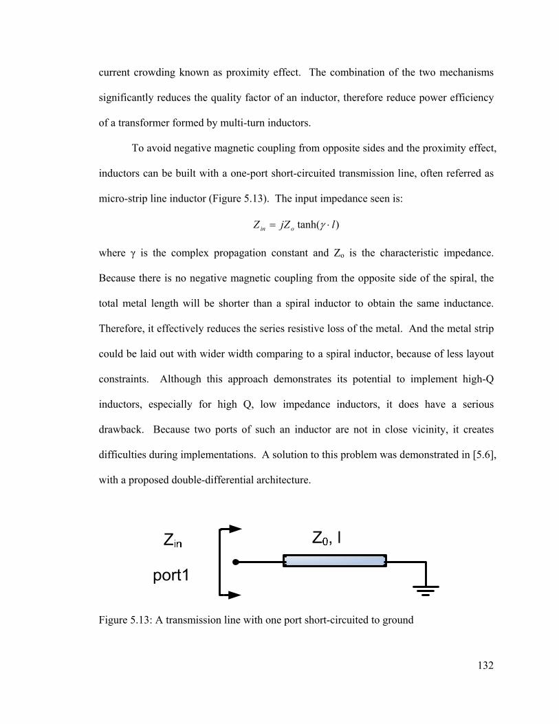
132
current crowding known as proximity effect. The combination of the two mechanisms
significantly reduces the quality factor of an inductor, therefore reduce power efficiency
of a transformer formed by multi-turn inductors.
To avoid negative magnetic coupling from opposite sides and the proximity effect,
inductors can be built with a one-port short-circuited transmission line, often referred as
micro-strip line inductor (Figure 5.13). The input impedance seen is:
)tanh( ljZZ oin ⋅= γ
where γ is the complex propagation constant and Zo is the characteristic impedance.
Because there is no negative magnetic coupling from the opposite side of the spiral, the
total metal length will be shorter than a spiral inductor to obtain the same inductance.
Therefore, it effectively reduces the series resistive loss of the metal. And the metal strip
could be laid out with wider width comparing to a spiral inductor, because of less layout
constraints. Although this approach demonstrates its potential to implement high-Q
inductors, especially for high Q, low impedance inductors, it does have a serious
drawback. Because two ports of such an inductor are not in close vicinity, it creates
difficulties during implementations. A solution to this problem was demonstrated in [5.6],
with a proposed double-differential architecture.
Figure 5.13: A transmission line with one port short-circuited to ground
133
A compromise between a multi-turn inductor and a micro-strip line inductor is a
single-turn inductor, sometime referred as “hairpin” inductor. In a single-turn inductor, if
the distance between opposite sides is large, negative magnetic coupling is negligible.
The inductance is primarily limited by back plane mirror current. Moreover, the
proximity effect in a single-turn inductor has little impact while the skin effect dominates
the high frequency loss. Hence, it behaves very much like a micro-strip line inductor of
the same total length. Unlike a micro-strip line inductor, the two ports are close by rather
than far away from each other, so that it is relatively straightforward to lay it out.
Figure 5.14 shows the three inductors implemented in the same technology but
with different style, micro-strip line, single-turn and multi-turn respectively. The metal
width of three inductors is kept same. The dimensions of the inductors are designed to
make them have roughly equal inductance. The inductance of three inductors are about
the same (0.6-nH ± 1%), simulated at 2-GHz with Momentum in Agilent ADS. The
quality factors of three inductors are 17, 11 and 7.9 respectively. We see that the micro-
strip line inductor has used the cross section area most efficiently, with current evenly
distributed, while in the multi-turn inductor, the current crowding is quite obvious,
especially in the inner turns where the magnetic field is large. However, the single-turn
inductor did not have expected performance. Its quality factor is lower than the micro-
strip line inductor. Depending on the distance between opposite sides, losses caused by
proximity effect and negative mutual coupling still have some impact on a single-turn
inductor and degrade its performance. Besides, two additional mechanisms degrade the
quality factor. First, the two ports of a single turn inductor are physically close to each
other, therefore part of the signal will leak through substrate and induce extra loss,

134
especially at high frequency. For micro-strip line inductors, two ports are away from
each other, the path through substrate is, therefore, a high impedance path. Very little
signal will take this path which effectively eliminates this loss. It should be noted this
loss could be significantly reduced in a single-turn or multi-turn inductor using a
patterned metal shield as ground plane. The other is due to the geometry of the single-
turn inductor. Circular geometry can improve the quality factor by 10~20% comparing to
octagonal geometry [5.7]. After changing the geometry to circular shape, the Q of the
single-turn inductor increased from 11 to 12 (Figure 5.15).
As mentioned before, micro-strip line inductors have superior quality factor,
nonetheless they impose much more constraints in implementation and will occupy more
area. In single-turn or multi-turn spiral inductors, current crowding degrades Q factors,
however, they usually occupy much less area comparing to micro-strip line inductors and
are easy to be laid out. Single-turn inductors are particularly of interest for low
impedance inductors. Quality factors of single-turn inductors or multi-turn inductors can
be further improved using interleave structure and/or other measures.
Cur
rent
Den
sity
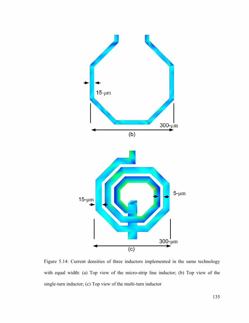
135
(c)300-µm
15-µm5-µm
Figure 5.14: Current densities of three inductors implemented in the same technology
with equal width: (a) Top view of the micro-strip line inductor; (b) Top view of the
single-turn inductor; (c) Top view of the multi-turn inductor
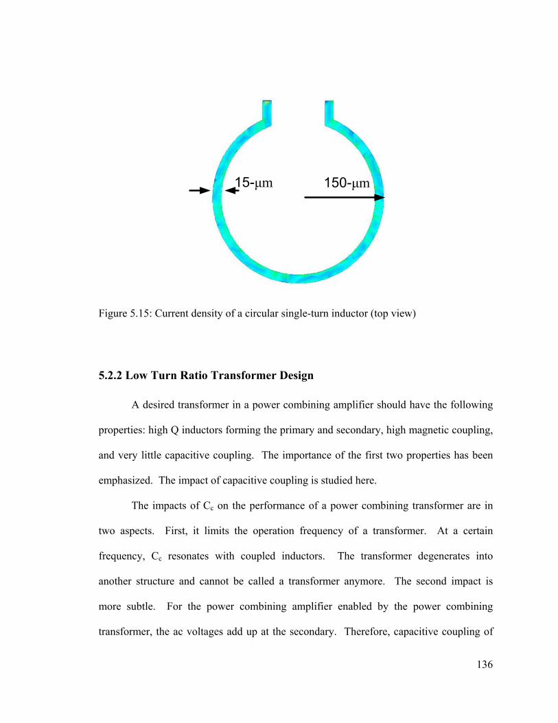
136
15-µm 150-µm
Figure 5.15: Current density of a circular single-turn inductor (top view)
5.2.2 Low Turn Ratio Transformer Design
A desired transformer in a power combining amplifier should have the following
properties: high Q inductors forming the primary and secondary, high magnetic coupling,
and very little capacitive coupling. The importance of the first two properties has been
emphasized. The impact of capacitive coupling is studied here.
The impacts of Cc on the performance of a power combining transformer are in
two aspects. First, it limits the operation frequency of a transformer. At a certain
frequency, Cc resonates with coupled inductors. The transformer degenerates into
another structure and cannot be called a transformer anymore. The second impact is
more subtle. For the power combining amplifier enabled by the power combining
transformer, the ac voltages add up at the secondary. Therefore, capacitive coupling of
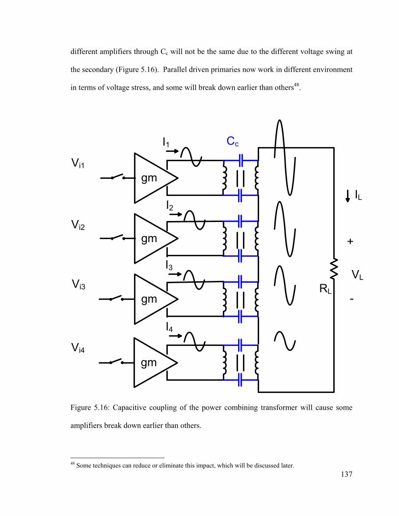
137
different amplifiers through Cc will not be the same due to the different voltage swing at
the secondary (Figure 5.16). Parallel driven primaries now work in different environment
in terms of voltage stress, and some will break down earlier than others48.
RL
I1
I2
I3
I4
IL
+
-
VL
Cc
gm
gm
gm
gm
Vi1
Vi2
Vi3
Vi4
Figure 5.16: Capacitive coupling of the power combining transformer will cause some
amplifiers break down earlier than others.
48 Some techniques can reduce or eliminate this impact, which will be discussed later.
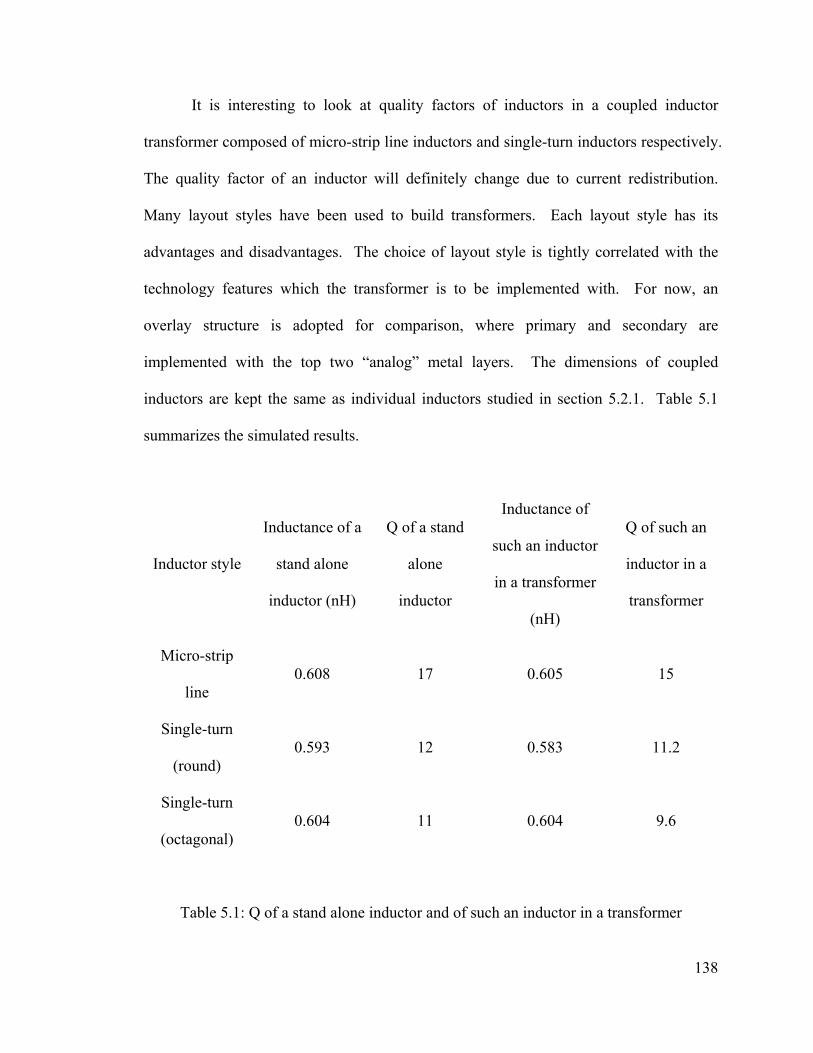
138
It is interesting to look at quality factors of inductors in a coupled inductor
transformer composed of micro-strip line inductors and single-turn inductors respectively.
The quality factor of an inductor will definitely change due to current redistribution.
Many layout styles have been used to build transformers. Each layout style has its
advantages and disadvantages. The choice of layout style is tightly correlated with the
technology features which the transformer is to be implemented with. For now, an
overlay structure is adopted for comparison, where primary and secondary are
implemented with the top two “analog” metal layers. The dimensions of coupled
inductors are kept the same as individual inductors studied in section 5.2.1. Table 5.1
summarizes the simulated results.
Inductor style
Inductance of a
stand alone
inductor (nH)
Q of a stand
alone
inductor
Inductance of
such an inductor
in a transformer
(nH)
Q of such an
inductor in a
transformer
Micro-strip
line 0.608 17 0.605 15
Single-turn
(round) 0.593 12 0.583 11.2
Single-turn
(octagonal) 0.604 11 0.604 9.6
Table 5.1: Q of a stand alone inductor and of such an inductor in a transformer
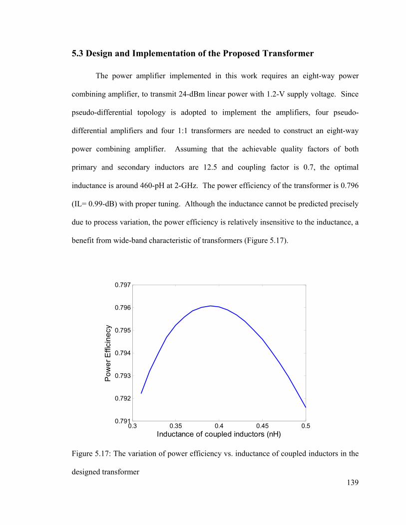
139
5.3 Design and Implementation of the Proposed Transformer
The power amplifier implemented in this work requires an eight-way power
combining amplifier, to transmit 24-dBm linear power with 1.2-V supply voltage. Since
pseudo-differential topology is adopted to implement the amplifiers, four pseudo-
differential amplifiers and four 1:1 transformers are needed to construct an eight-way
power combining amplifier. Assuming that the achievable quality factors of both
primary and secondary inductors are 12.5 and coupling factor is 0.7, the optimal
inductance is around 460-pH at 2-GHz. The power efficiency of the transformer is 0.796
(IL= 0.99-dB) with proper tuning. Although the inductance cannot be predicted precisely
due to process variation, the power efficiency is relatively insensitive to the inductance, a
benefit from wide-band characteristic of transformers (Figure 5.17).
0.3 0.35 0.4 0.45 0.50.791
0.792
0.793
0.794
0.795
0.796
0.797
Inductance of coupled inductors (nH)
Pow
er E
ffici
necy
Figure 5.17: The variation of power efficiency vs. inductance of coupled inductors in the
designed transformer

140
Because the chosen process offers two thick top metal layers, overlay structure is
used to implement the power combining transformer. This structure can provide good
magnetic coupling without excessive capacitive coupling. The primaries are
implemented with lower level top metal and the secondary is implemented with the upper
top metal. In this way, primaries act as good electric shield to prevent the displacement
current flowing from the high voltage swing secondary to the substrate as well as
electrical coupling to the other part of the circuits. Patterned ground shield with M1
provides further isolation. Inductors are implemented with single-turn style for both
primaries and the secondary. Ideally, a circular shape would be favored to obtain high
quality factor, however, it is prohibited by the design rules of the process.
A simple transformer layout is shown in Figure 5.18. In this approach, the
adjacent windings have current flowing in opposite direction, and thus do not contribute
as much flux and coupling to the secondary. Hence, power efficiency will be hurt.
Moreover, since primaries will have different magnetic coupling to the secondary, a
different load will be seen at each primary which causes severely degraded performance.
Several measures can be taken to minimize coupling of the adjacent windings.
One of them is to leverage the fact that orthogonal lines have negligible magnetic
coupling as shown in Figure 5.19. This approach still has one flaw, which is the
degradation of quality factors from those 90° corners. A compromise is made as shown
in Figure 5.20. Now the primary inductors look like an oval. And windings are kept
apart with some distance to minimize internal flux cancellation.
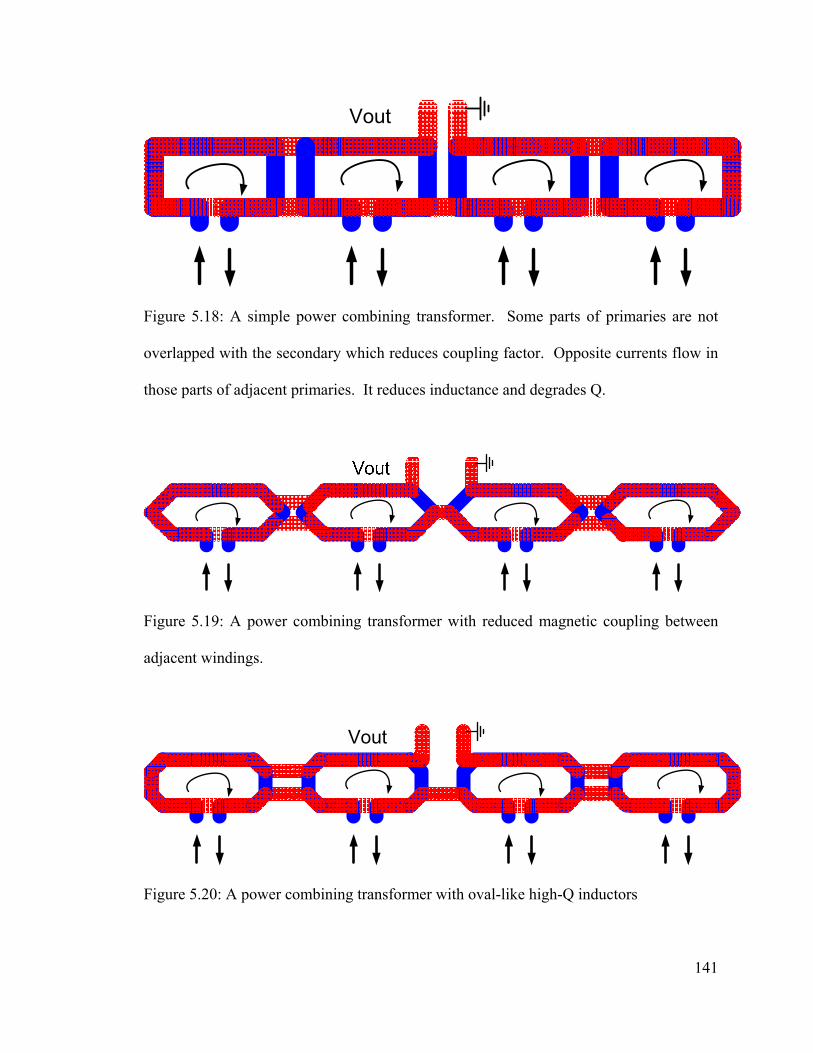
141
Vout
Figure 5.18: A simple power combining transformer. Some parts of primaries are not
overlapped with the secondary which reduces coupling factor. Opposite currents flow in
those parts of adjacent primaries. It reduces inductance and degrades Q.
Figure 5.19: A power combining transformer with reduced magnetic coupling between
adjacent windings.
Vout
Figure 5.20: A power combining transformer with oval-like high-Q inductors
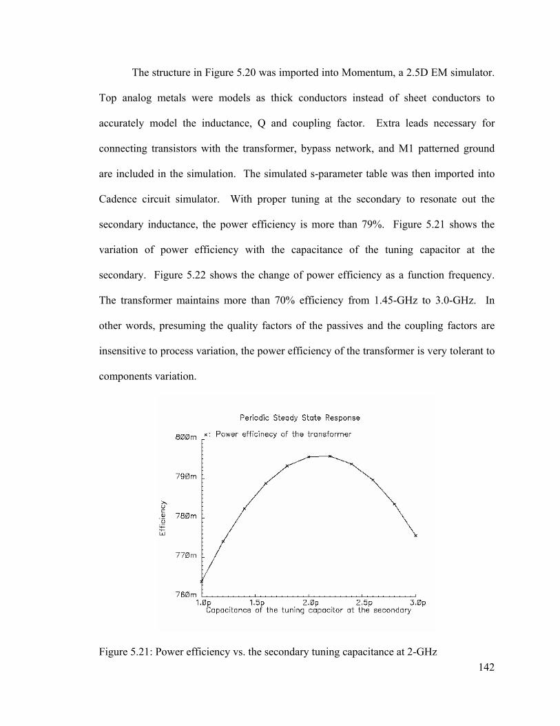
142
The structure in Figure 5.20 was imported into Momentum, a 2.5D EM simulator.
Top analog metals were models as thick conductors instead of sheet conductors to
accurately model the inductance, Q and coupling factor. Extra leads necessary for
connecting transistors with the transformer, bypass network, and M1 patterned ground
are included in the simulation. The simulated s-parameter table was then imported into
Cadence circuit simulator. With proper tuning at the secondary to resonate out the
secondary inductance, the power efficiency is more than 79%. Figure 5.21 shows the
variation of power efficiency with the capacitance of the tuning capacitor at the
secondary. Figure 5.22 shows the change of power efficiency as a function frequency.
The transformer maintains more than 70% efficiency from 1.45-GHz to 3.0-GHz. In
other words, presuming the quality factors of the passives and the coupling factors are
insensitive to process variation, the power efficiency of the transformer is very tolerant to
components variation.
Figure 5.21: Power efficiency vs. the secondary tuning capacitance at 2-GHz

143
Figure 5.22: Power efficiency vs. frequency for a transformer designed at 2-GHz
The high efficiency achieved by this transformer undoubtedly benefited from
double thick “analog” metals (~3-µm) available in the process. In a typical digital CMOS
process, however, only one thick top metal is available. Obviously, a different style is
needed.
5.4 Discussions and Summary
In a typical digital CMOS process, only one thick metal is provided. Therefore,
lateral coupling structure has to be used which could potentially degrade power efficiency
from two aspects. First, the magnetic coupling will not be as good as an overlay structure.
Second, the inner conductor will suffer from current crowding which results from the
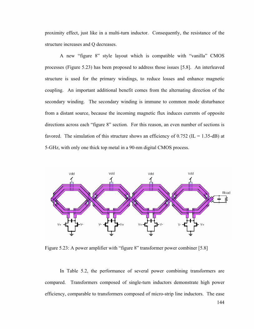
144
proximity effect, just like in a multi-turn inductor. Consequently, the resistance of the
structure increases and Q decreases.
A new “figure 8” style layout which is compatible with “vanilla” CMOS
processes (Figure 5.23) has been proposed to address those issues [5.8]. An interleaved
structure is used for the primary windings, to reduce losses and enhance magnetic
coupling. An important additional benefit comes from the alternating direction of the
secondary winding. The secondary winding is immune to common mode disturbance
from a distant source, because the incoming magnetic flux induces currents of opposite
directions across each “figure 8” section. For this reason, an even number of sections is
favored. The simulation of this structure shows an efficiency of 0.752 (IL = 1.35-dB) at
5-GHz, with only one thick top metal in a 90-nm digital CMOS process.
Figure 5.23: A power amplifier with “figure 8” transformer power combiner [5.8]
In Table 5.2, the performance of several power combining transformers are
compared. Transformers composed of single-turn inductors demonstrate high power
efficiency, comparable to transformers composed of micro-strip line inductors. The ease
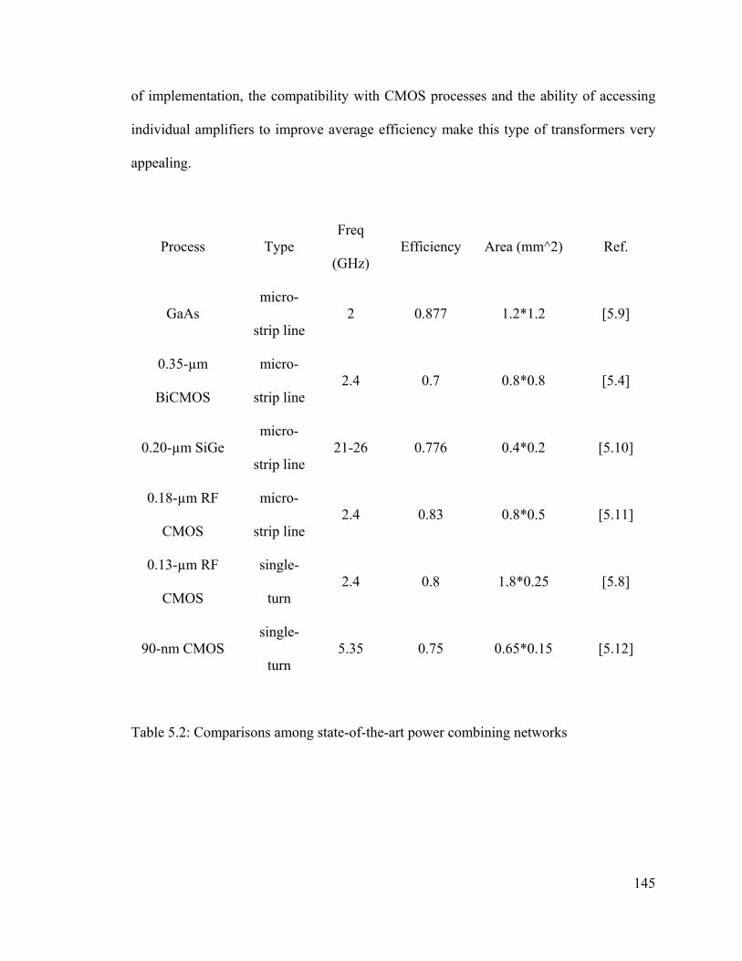
145
of implementation, the compatibility with CMOS processes and the ability of accessing
individual amplifiers to improve average efficiency make this type of transformers very
appealing.
Process Type Freq
(GHz) Efficiency Area (mm^2) Ref.
GaAs micro-
strip line 2 0.877 1.2*1.2 [5.9]
0.35-µm
BiCMOS
micro-
strip line 2.4 0.7 0.8*0.8 [5.4]
0.20-µm SiGe micro-
strip line 21-26 0.776 0.4*0.2 [5.10]
0.18-µm RF
CMOS
micro-
strip line 2.4 0.83 0.8*0.5 [5.11]
0.13-µm RF
CMOS
single-
turn 2.4 0.8 1.8*0.25 [5.8]
90-nm CMOS single-
turn 5.35 0.75 0.65*0.15 [5.12]
Table 5.2: Comparisons among state-of-the-art power combining networks
146
5.5 References
[5.1] T.H. Lee, “The design of CMOS radio-frequency integrated circuits”, 1st Edition,
Cambridge University Press, 1998
[5.2] R. Ludwig, P. Bretchko, “RF circuit design – theory and applications”, Prentice-
Hall, Inc, 2000
[5.3] R. E. Collin, “Foundations for Microwave Engineering”, Second Edition, IEEE
Press, N.Y. 2001
[5.4] I. Aoki, S. Kee, D. B. Rutledge and A. Hajimiri, “Distributed active transformer: A
new power combining and impedance transformation technique,” IEEE Trans. Micro.
Theory Tech., vol. 50, no. 1, pp. 316–331, January 2002.
[5.5] M.Y. Bohsali, A.M. Niknejad, “Microwave performance of monolithic silicon
passive transformers”, RFIC Symp. Dig. of Papers, pp. 647-650, June 2004
[5.6] I. Aoki, S. Kee, D. B. Rutledge and A. Hajimiri, “Fully integrated CMOS power
amplifier design using the Distributive Active-Transformer architecture”, IEEE J. Solid-
State Circuits, vol. 37, no. 3, pp. 371-383, March 2002
[5.7] I.J. Bahl, “High performance inductors”, IEEE Trans. Micro. Theory Tech., vol. 49,
no. 4, pp. 654-664, April 2001
[5.8] G. Liu, T.-J. King Liu, A.M. Niknejad, “A 1.2V, 2.4GHz Fully Integrated Linear
CMOS Power Amplifier with Efficiency Enhancement”, Custom Integrated Circuits
Conference, September 2006
[5.9] S. Kim, K. Lee, J. Lee, B. Kim, S.D. Kee, I.Aoki, D.B. Rutledge, “An optimized
design of distributed active transformer”, IEEE Trans. Microwave Theory Tech., vol. 53,
no. 1, pp. 380-388, January 2005

147
[5.10] T.S.D. Cheung and J.R. Long, “A 21-26-GHz SiGe bipolar power amplifier
MMIC,” IEEE J. Solid-State Circuits, vol. 40, no. 12,pp. 2583–2597, December 2005
[5.11] J. Kang, A. Hajimiri, and B. Kim, “A Single-Chip Linear CMOS Power Amplifier
for 2.4GHz WLAN,” IEEE ISSCC Digest of Technical Papers, pp. 208-209, February
2006
[5.12] P. Haldi, G. Liu, A.M. Niknejad, “CMOS compatible transformer power
combiner”, Electronics Letter, vol. 42, no. 19, pp. 1091-1092, September 2006
148
Chapter 6. A Fully Integrated CMOS Power Amplifier with
Average Efficiency Enhancement
6.1 Design of the prototype
6.2 Layout considerations
6.3 The CMOS prototype
6.4 Experimental Results
6.5 Summary
6.6 References
A prototype was implemented in a 0.13-µm CMOS process to prove the concept
of the power control and efficiency enhancement technique proposed in this work. The
prototype is based on a power combining transformer described in Section 4.3 centered
around 2.4-GHz, with the ability to transmit 24-dBm at the P-1dB compression point under
1.2-V supply. The average efficiency should be good as well as the instantaneous
efficiency at the peak output power. In this chapter, the design process will be
highlighted, with some discussion of practical issues. The design methodology took a
top-down approach, with several iterations in some critical steps. This methodology
proved to be very effective. Although the prototype was not designed for any particular
standards, it was tested with both continuous wave (CW) signals and modulated signals.
149
6.1 Design of the Prototype
6.1.1 Features of the CMOS Process
A 0.13-µm RF CMOS process was used to implement the prototype. This process
offers two thick analog top metal layers for high-Q inductors, MIM capacitors, 1.2-V
core transistors, 3.3-V I/O transistors and other devices. It should be noted that only
thick top metals and MIM capacitors are Analog/RF options. All other features are also
standard in a digital CMOS process. As discussed in Chapter 3, the use of I/O transistors
has several drawbacks. Furthermore, I/O transistors will scale as well as process scaling
continues. Based on those considerations, only thin-oxide core transistors were
employed to implement the prototype. This implies a low supply voltage for the power
amplifier.
6.1.2 PA Architecture
At the beginning of the design, one of the most important decisions to make was
to choose the class of operation for the power amplifier. The class-AB mode was chosen
for good reasons. It is a classical compromise, offering higher efficiency than “linear”
class-A mode, with some increased nonlinear effects which can be tolerated. No
linearization scheme was employed around the amplifier. The purpose is to determine
the intrinsic linearity of CMOS power amplifiers with deeply scaled devices.
A power amplifier can be divided into three major blocks, an input matching
network, active devices and an output matching network. Input matching is certainly
critical because it plays an important role in determining the power amplifier gain.

150
Hence it will affect the power added efficiency (PAE). Nonetheless, good drain
efficiency usually implies good PAE in class-AB transconductance power amplifiers,
because the gain of each stage is usually around 10~12-dB. Furthermore, it should be
noted that the major challenge of fully integrated CMOS power amplifier designs lies in
the integration of the output matching network. In the implemented prototype, the output
matching network of the power amplifier was emphasized, while input matching was not
implemented.
6.1.3 Power Combining
The targeted linear power of this work is 24-dBm at P-1dB. The supply voltage is
predetermined to be 1.2-V, the same as the supply voltage for the baseband circuitry in
the same technology. To determine how many individual amplifiers are needed for
power combining for the peak output power, some assumptions have to be made at the
design stage. Assuming that saturation voltage Vdsat is 0.1-V and the efficiency of the
overall amplifier is between 25% and 35%, the total output power of the N-way
transformer power combining amplifier is:
NNR
VVPL
dsatDDout ⋅
−⋅=
/)(
21 2
η
so N is derived as:
2)(2
dsatDD
Lout
VVRPN
−⋅⋅⋅
=η
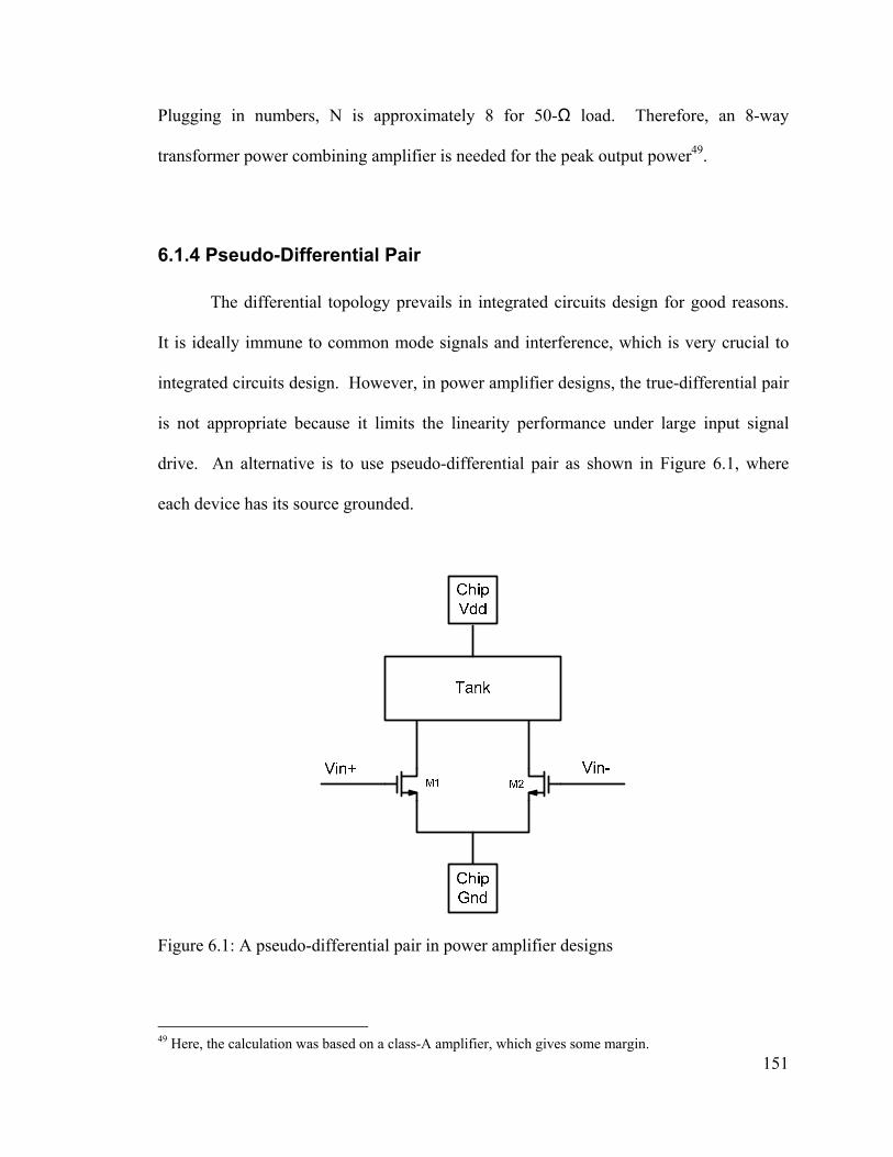
151
Plugging in numbers, N is approximately 8 for 50-Ω load. Therefore, an 8-way
transformer power combining amplifier is needed for the peak output power49.
6.1.4 Pseudo-Differential Pair
The differential topology prevails in integrated circuits design for good reasons.
It is ideally immune to common mode signals and interference, which is very crucial to
integrated circuits design. However, in power amplifier designs, the true-differential pair
is not appropriate because it limits the linearity performance under large input signal
drive. An alternative is to use pseudo-differential pair as shown in Figure 6.1, where
each device has its source grounded.
Figure 6.1: A pseudo-differential pair in power amplifier designs
49 Here, the calculation was based on a class-A amplifier, which gives some margin.
152
Several key benefits of pseudo-differential pair are very important to integrated
power amplifier designs. The fundamental frequency components of the two device
currents will be equal in amplitude and opposite in phase. In fact, this applies to all other
odd-order harmonics. Therefore, this creates a low-loss on-chip AC-ground at the
common source node and VDD supply node, which significantly minimizes the impact of
package parasitics on power amplifier performance. Under typical conditions, the output
is taken differentially so that even-order harmonics are suppressed at the output. Hence,
this relaxes the filtering requirements at the output to meet stringent spurious tone
emission specifications. In addition, signals injected into the substrate are even order
harmonics. Therefore, the impact on the performance of other circuit blocks that are on
the same chip is substantially reduced. The most important benefit, in the context of
power amplifier designs, is doubling the voltage swing at the output. In fact, a pseudo-
differential amplifier is equivalent to a 2-way power combined amplifier. Therefore, in
the prototype, four pseudo-differential amplifiers are needed to form an 8-way
transformer power combining amplifier.
6.1.5 Transconductor Design
Although RF performance of CMOS devices has been greatly improved in
parallel with the rapid technology evolution, it can be severely compromised by parasitics.
This is especially true for power transistors. The gate-width of a power transistor is
usually very large and can reach several millimeters to achieve desired gain and output
power. For instance, let’s calculate the poly gate resistance of a transistor with
dimensions of 2000-µm/0.13-µm, assuming the sheet resistance Rsheet is 10-Ω/square:
153
Ω=⋅= KL
WRR sheetG 153
Recall that in Chapter 3:
GDGTSGDS
T
CRfRRgff
π2)(1
2max ++=
With more than 100-kΩ in series with gate, the fmax of the device is certainly not
acceptable. Hence, a multi-finger structure with small finger gate width is necessary to
reduce gate resistance in order to operate power transistor in RF frequencies. However,
as number of fingers (NF) increases, the layout of the power transistor becomes
cumbersome. Gradually, extrinsic layout parasitics will dominate over intrinsic parasitics
to degrade the RF performance. Figure 6.2 shows a power transistor with some parasitic
elements. The source parasitic components cause RF voltage feedback and reduce the
gain. The gate and drain parasitic elements induce some non-negligible delay along the
signal path, so that output of each individual transistor cannot be added up in phase
perfectly.
Figure 6.2: A transistor model for power transistors including inductive and resistive
parasitic elements
154
Yet another design trade-off to make is about the substrate resistance. Figure 6.3
illustrates a model of a NMOS device in common-source configuration with a simple
substrate network. If Rsub is large, the transistor performance at RF frequency will be
compromised. This could be explained in the following manner. An input signal applied
at the gate of the common-source transistor will generate an out-of-phase voltage at the
drain. At high frequencies, the large voltage swing at the drain will induce a voltage
swing at the back gate (body node). The input signal at the gate and the induced signal at
the back gate are out of phase, leading to transconductance degradation at high
frequencies 50 . The output impedance degradation at high frequencies can also be
explained in a similar way. Besides, this parasitic resistance consumes signal power.
Therefore, Rsub of the transconductor should be properly minimized. The substrate
resistance Rsub is determined by the distance from substrate contacts to the actual
transistor. Rsub is reduced by placing substrate contacts close to the transistor.
Proper biasing of the power transistor is important, because the operating point
affects the intrinsic linearity directly. It is well known that the superposition of
nonlinearities in the transfer characteristic can reduce/cancel some undesirable
nonlinearities. This indeed is the fundamental of class-AB operation [6.1 – 6.3]51. In the
prototype, the gm of the transconductor is one of the major sources of nonlinearity. When
MOS transistors are biased from weak inversion region to moderate and strong inversion
region, the third-order term gm,3 changes its sign from positive to negative. By biasing
the transistor in the weak inversion region (slightly above threshold voltage), the
effective average gm,3 can be reduced to zero, hence improving the linearity. At RF
50 This is quite obvious from small-signal model. 51 It should be noted, it only considers AM-AM nonlinearity. In some applications, such as multi-carrier system, AM-PM is more important.
155
frequencies, the effectiveness of this method can be compromised, because even-order
distortion products will feed back through lead inductance, interact with fundamental
signals and generate IM products falling into the interested band. In fact, the second-
order term gm,2 peaks at the biasing point corresponding to minimum gm,3. Therefore,
even-order terms need to be properly terminated in order to obtain good linearity. This
can be done by placing a second order harmonic “trap”, an LC tank, at the drain and the
source [6.4], or by placing a large bypass capacitor to reduce voltage swing generated by
even-order harmonics as used in this work.
Figure 6.3: A device model of a common-source NMOS transistor with a simple substrate
network. Cjs and Cjd are junction capacitance of source and drain respectively. Rb is the
effective body resistance. Rsub represents substrate resistance.
6.1.6 Cascode Transistor Design
The cascode configuration was employed to ensure reliable operations with 1.2-V
supply voltage. Furthermore, it offers several other benefits such as higher gain and

156
reduced Miller feedback. However, the cascode topology does pose some risks on the
stability of the PA.
A simplified model is shown in Figure 6.4(b). Looking into the gate of the
cascode device m2, the input impedance is:
pargs
m
pargsin CCs
gsCsC
Z 2211
++=
The real part is:
pargs
m
CCsgZin 2
2)Re( =
Obviously it is negative. This definitely poses concerns on the stability of the circuit.
There should not be any surprise, since the circuit in Figure 6.4(b) looks like a Colpitts
oscillator. Careful design and layout is required to suppress this potential oscillation.
Figure 6.4: (a) A simplified cascode configuration, where m1 is the transconductor device
and m2 is the cascode device; (b) An equivalent model for stability analysis.

157
For convenience, usually the cascode transistor is connected with the supply,
although this is neither the only nor the best choice. The size of the cascode transistor is
determined after considering several trade-offs. As discussed in Chapter 4, the size and
the bias of the cascode transistor will affect the gain, output power and efficiency.
Another consideration on the cascode transistor design is AM-PM compensation. The
cascode configuration consists of a common-source transistor and a common-gate
transistor. Due to the fact that the common-source transistor delivers the output power
out-of-phase while the common-gate transistor delivers the output power in phase, their
AM-PM conversion at near saturation region are expected to have opposite behaviors
[6.5].
The cascode common-gate transistor design is as important as the common-source
transconductor design. The design process is rather interactive with the transconductor
design, therefore, the design needs several iterations in order to obtain optimum
performance.
6.1.7 Output Matching Network – Transformer Power Combiner
The output matching network was designed based on the transformer power
combiner described in Chapter 5. It plays two important roles. First, it acts as an
impedance transformation network, and combines power from each individual amplifier.
Second, it converts a differential signal into a single-ended signal so it can be connected
to an antenna directly52. High efficiency of the transformer is the prerequisite in order to
52 Although differential circuits prevail in transceiver and baseband circuits, almost all the power amplifiers in the market today are single-ended. If the differential topology is employed, a balun is required to convert a differential signal to a single-ended signal. Typical loss of a balun at RF frequencies is around 1-

158
achieve high efficiency of the entire PA. High component Q and tight magnetic coupling
are crucial to reduce the loss in the transformer. One-turn “hair pin” style inductors are
implemented to construct the primary and the secondary coils of the transformer. To
improve the magnetic coupling, an overlay structure is adopted wherein the secondary
coil is placed directly on top of the primary coils. The magnetic coupling factor k is ~0.7
with this structure. A metal shield (M1) is used to reduce capacitive coupling to the
conductive substrate. The efficiency of the on-chip transformer is approximately 80%,
simulated with ADS Momentum and HFSS.
At power back-off, some amplifiers are turned off, the matching network need be
reconfigured to maintain reasonable efficiency. The reconfiguration is necessary due to
two reasons. First, the transformer is a passive device, which means it is bilateral. Figure
6.5 shows an equivalent model for a power combining amplifier. Although two
amplifiers are turned off, signals on the secondary of the transformer will still be
transformed to the primaries and some power is dissipated due to the inductor loss.
Therefore, as the amplifier is turned off, the corresponding primary side of the
transformer should be reconfigured to minimize this loss.
Second, the impedance seen by the amplifiers remaining on will vary as other
amplifiers turned off. To maintain optimum output impedance seen by the amplifiers
remaining on, the corresponding primary sides of the transformer also need to be
reconfigured to obtain optimum performance53 . The detailed hand analysis is very
complicated, and the result is highly depended on the transformer style itself. In practice,
dB. And such a balun is costly and occupies lots of board space. Hence, a differential PA is very hard to sell in the market. In this work, a balun is not needed in the design which offers a great advantage. 53 The secondary will have large swing, and it is better to leave intact.
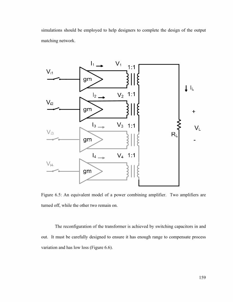
159
simulations should be employed to help designers to complete the design of the output
matching network.
Figure 6.5: An equivalent model of a power combining amplifier. Two amplifiers are
turned off, while the other two remain on.
The reconfiguration of the transformer is achieved by switching capacitors in and
out. It must be carefully designed to ensure it has enough range to compensate process
variation and has low loss (Figure 6.6).

160
Figure 6.6: A switched capacitor array. This configuration takes advantage of differential
operation to minimize switch losses without the need for large size switches.
6.1.8 Stability
Almost every PA design is susceptible to unwanted and potentially destructive
oscillations in power amplifiers. Extra attention paid during the design stage should
eliminate this risk, or at least make it less likely. Stability analysis available in circuit
simulators assumes the entire circuit is linear, although power amplifiers are very
nonlinear. To get around this issue, stability analysis is performed while sweeping the
operating point in order to gain insights into the stability of the power amplifier under
large signal operation. Of course, transient analysis is always needed as the final check54.
For the proposed power combining amplifier, the inputs of each individual
amplifier are connected with interconnects. Because the dimensions of the layout are
rather large, those interconnects behave like transmission lines. This, in turn, gives a
potential oscillation problem, odd mode oscillation, which is a common problem in
54 It was found that small-signal stability analysis across swept operating points is a very good indicator of the stability under large signal operation.
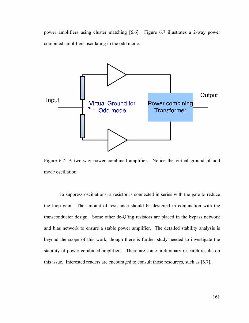
161
power amplifiers using cluster matching [6.6]. Figure 6.7 illustrates a 2-way power
combined amplifiers oscillating in the odd mode.
Figure 6.7: A two-way power combined amplifier. Notice the virtual ground of odd
mode oscillation.
To suppress oscillations, a resistor is connected in series with the gate to reduce
the loop gain. The amount of resistance should be designed in conjunction with the
transconductor design. Some other de-Q’ing resistors are placed in the bypass network
and bias network to ensure a stable power amplifier. The detailed stability analysis is
beyond the scope of this work, though there is further study needed to investigate the
stability of power combined amplifiers. There are some preliminary research results on
this issue. Interested readers are encouraged to consult those resources, such as [6.7].
162
6.2 Layout Considerations
The importance of layout in power amplifier designs needs no introduction. In
this section, several practical considerations are presented. However, it should be noted
that there are many ways to layout one structure. Trade-offs have to be made based on
different considerations of each individual case.
6.2.1 Transconductor Layout
Based on the considerations discussed previously, a large power transistor can be
obtained by connecting unit cells in parallel. The dimension of the unit cell is determined
by trade-offs discussed before. The distance between unit cells is another factor under
consideration by the designer during layout. Decreasing of this distance is of course the
advantage from integration density perspective. However, this results in higher chip
temperature due to heat flow degradation. If the distance is too large, parasitic elements
will degrade the RF performance. In order to minimize the source resistance, which
degrades the gain, output power and efficiency, the source electrode is contacted on both
sides of the transistor.
Assembling smaller unit transistors into a much larger power transistor entails a
trade-off between the chip size and the delay equalization. Transistors are typically laid
out in grid fashion without considering the delay along the signal path to each transistor
(Figure 6.8). This approach will not cause any problem when the transistor is small.
However, for power transistors, it will degrade the performance greatly, since signals
from each unit transistor will not sum up in phase. Furthermore, some unit transistors
experience excessive voltage drops comparing to others, and current is not evenly
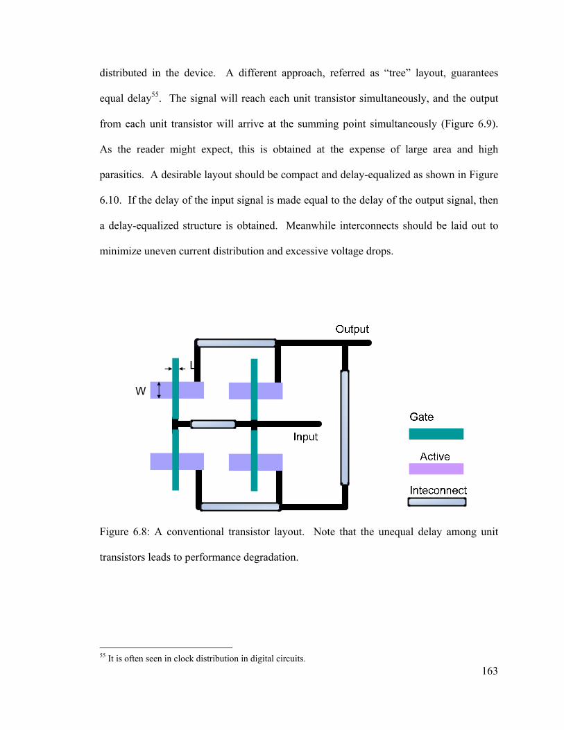
163
distributed in the device. A different approach, referred as “tree” layout, guarantees
equal delay55. The signal will reach each unit transistor simultaneously, and the output
from each unit transistor will arrive at the summing point simultaneously (Figure 6.9).
As the reader might expect, this is obtained at the expense of large area and high
parasitics. A desirable layout should be compact and delay-equalized as shown in Figure
6.10. If the delay of the input signal is made equal to the delay of the output signal, then
a delay-equalized structure is obtained. Meanwhile interconnects should be laid out to
minimize uneven current distribution and excessive voltage drops.
L
W
Figure 6.8: A conventional transistor layout. Note that the unequal delay among unit
transistors leads to performance degradation.
55 It is often seen in clock distribution in digital circuits.
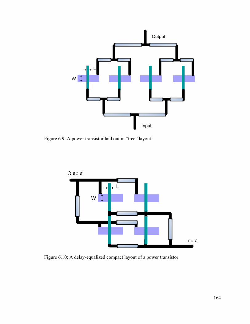
164
L
W
Output
Input
Figure 6.9: A power transistor laid out in “tree” layout.
L
W
Figure 6.10: A delay-equalized compact layout of a power transistor.
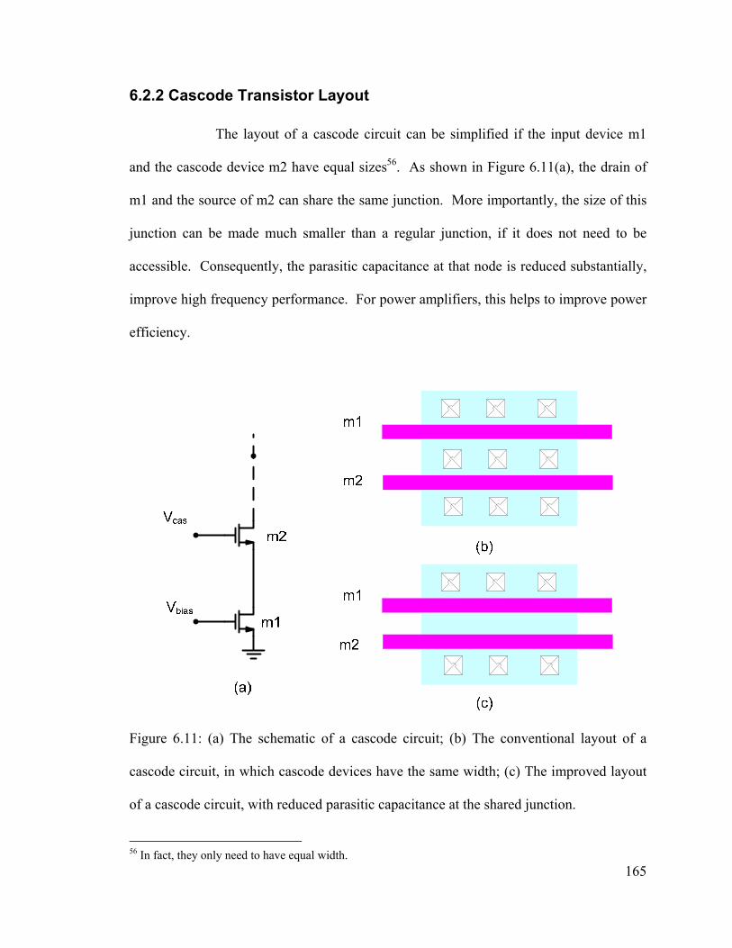
165
6.2.2 Cascode Transistor Layout
The layout of a cascode circuit can be simplified if the input device m1
and the cascode device m2 have equal sizes56. As shown in Figure 6.11(a), the drain of
m1 and the source of m2 can share the same junction. More importantly, the size of this
junction can be made much smaller than a regular junction, if it does not need to be
accessible. Consequently, the parasitic capacitance at that node is reduced substantially,
improve high frequency performance. For power amplifiers, this helps to improve power
efficiency.
Figure 6.11: (a) The schematic of a cascode circuit; (b) The conventional layout of a
cascode circuit, in which cascode devices have the same width; (c) The improved layout
of a cascode circuit, with reduced parasitic capacitance at the shared junction.
56 In fact, they only need to have equal width.
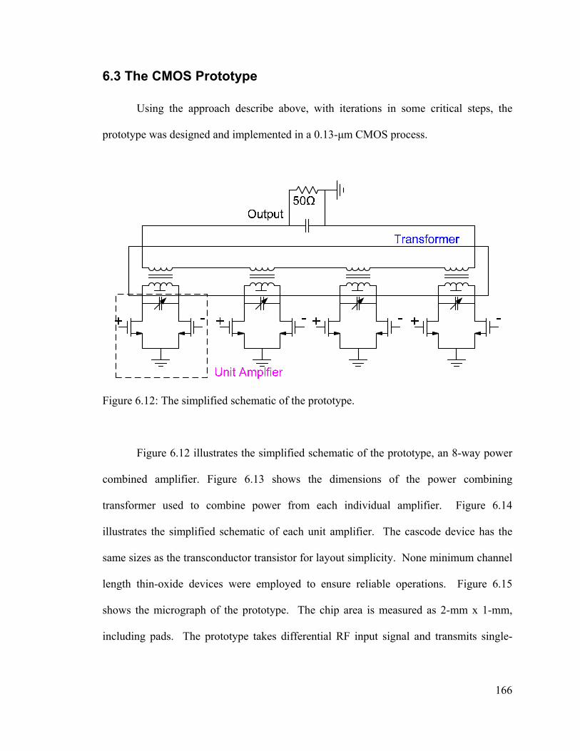
166
6.3 The CMOS Prototype
Using the approach describe above, with iterations in some critical steps, the
prototype was designed and implemented in a 0.13-µm CMOS process.
Figure 6.12: The simplified schematic of the prototype.
Figure 6.12 illustrates the simplified schematic of the prototype, an 8-way power
combined amplifier. Figure 6.13 shows the dimensions of the power combining
transformer used to combine power from each individual amplifier. Figure 6.14
illustrates the simplified schematic of each unit amplifier. The cascode device has the
same sizes as the transconductor transistor for layout simplicity. None minimum channel
length thin-oxide devices were employed to ensure reliable operations. Figure 6.15
shows the micrograph of the prototype. The chip area is measured as 2-mm x 1-mm,
including pads. The prototype takes differential RF input signal and transmits single-
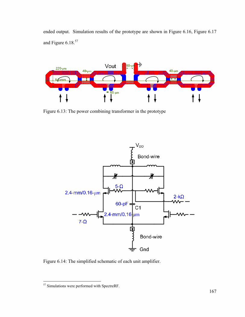
167
ended output. Simulation results of the prototype are shown in Figure 6.16, Figure 6.17
and Figure 6.18.57
Figure 6.13: The power combining transformer in the prototype
Figure 6.14: The simplified schematic of each unit amplifier.
57 Simulations were performed with SpectreRF.
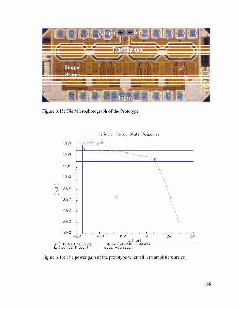
168
Figure 6.15: Die Microphotograph of the Prototype
Figure 6.16: The power gain of the prototype when all unit amplifiers are on.
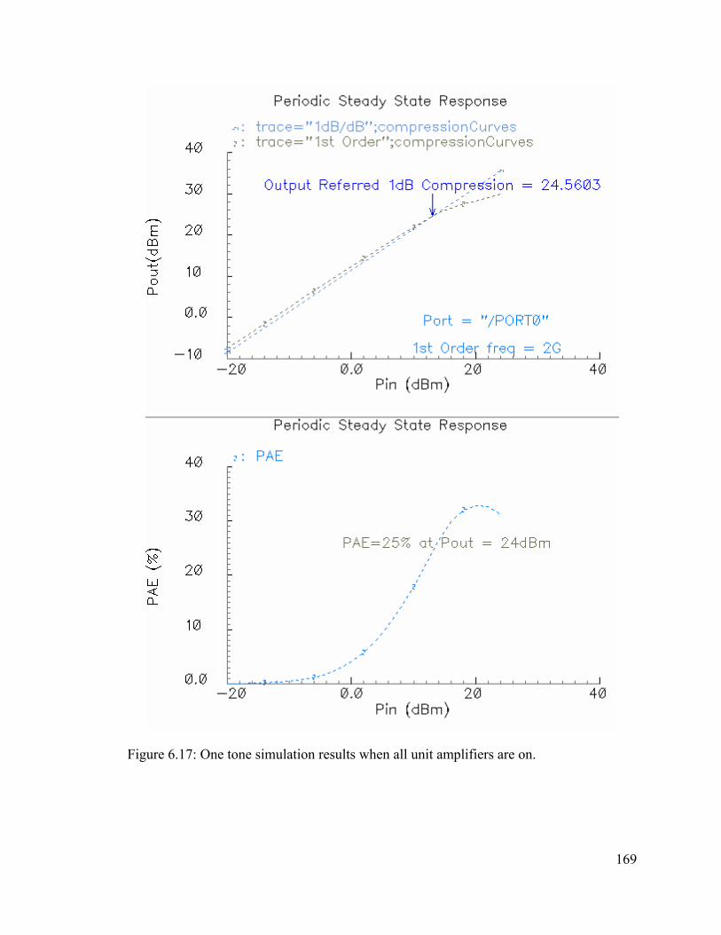
169
Figure 6.17: One tone simulation results when all unit amplifiers are on.
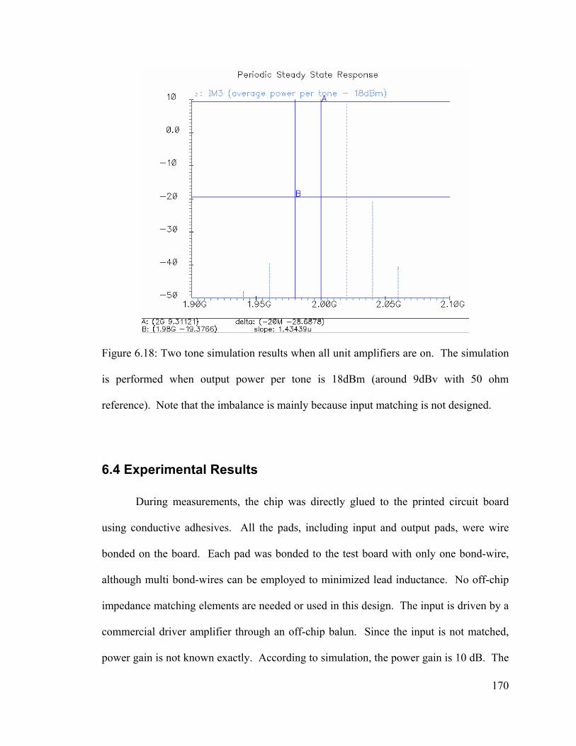
170
Figure 6.18: Two tone simulation results when all unit amplifiers are on. The simulation
is performed when output power per tone is 18dBm (around 9dBv with 50 ohm
reference). Note that the imbalance is mainly because input matching is not designed.
6.4 Experimental Results
During measurements, the chip was directly glued to the printed circuit board
using conductive adhesives. All the pads, including input and output pads, were wire
bonded on the board. Each pad was bonded to the test board with only one bond-wire,
although multi bond-wires can be employed to minimized lead inductance. No off-chip
impedance matching elements are needed or used in this design. The input is driven by a
commercial driver amplifier through an off-chip balun. Since the input is not matched,
power gain is not known exactly. According to simulation, the power gain is 10 dB. The

171
amplifier was tested with a 1.2V power supply. The cascode node was tied to the power
supply. It drew 114mA DC current without RF signals applied.
6.4.1 CW Signal Test
The output was directly connected to a power meter with two 6-dB attenuators for
power measurements. All system losses were calibrated out, while the measured results
included losses on the board and bond wire losses. Output power and drain efficiency
versus input power (read from the signal generator) for a single-tone test is shown in
Figure 6.19. The PA transmits up to 24-dBm linear power with 25% drain efficiency,
centered at 2.4-GHz. When driven into saturation, it delivers 27-dBm power with 32%
drain efficiency.
-20 -10 0 10 200
5
10
15
20
25
30
35
Pou
t (dB
m)
-20 -10 0 10 200
5
10
15
20
25
30
35
Pin (dBm)
Dra
in E
ffici
ency
(%)
Pout
Drain Efficiency
Figure 6.19: Measured output power and drain efficiency from single-tone test.
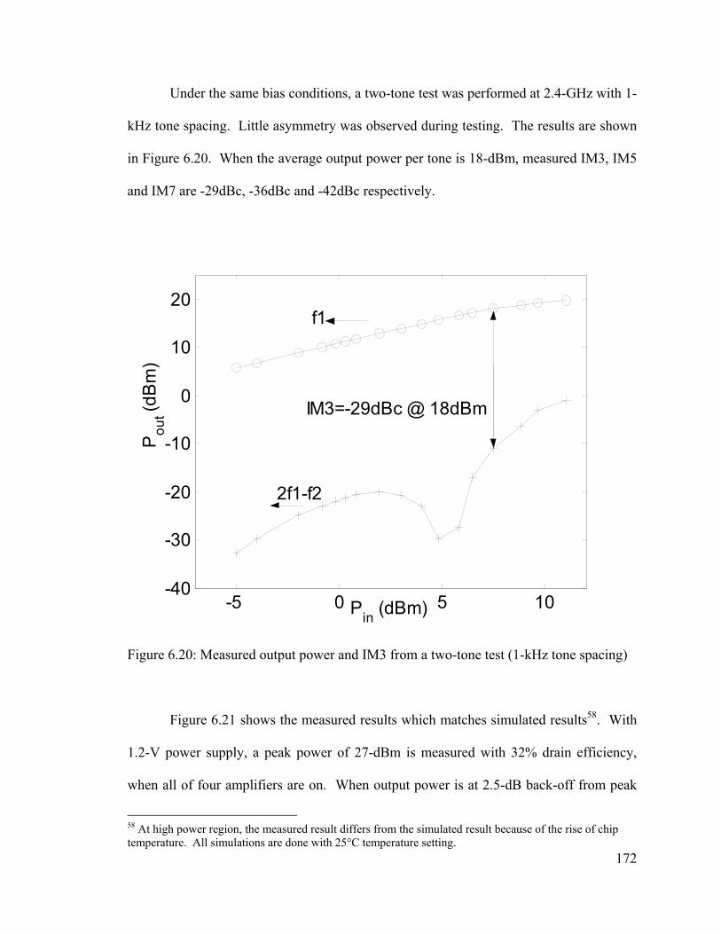
172
Under the same bias conditions, a two-tone test was performed at 2.4-GHz with 1-
kHz tone spacing. Little asymmetry was observed during testing. The results are shown
in Figure 6.20. When the average output power per tone is 18-dBm, measured IM3, IM5
and IM7 are -29dBc, -36dBc and -42dBc respectively.
-5 0 5 10-40
-30
-20
-10
0
10
20
Pin (dBm)
Pou
t (dB
m)
f1
2f1-f2
IM3=-29dBc @ 18dBm
Figure 6.20: Measured output power and IM3 from a two-tone test (1-kHz tone spacing)
Figure 6.21 shows the measured results which matches simulated results58. With
1.2-V power supply, a peak power of 27-dBm is measured with 32% drain efficiency,
when all of four amplifiers are on. When output power is at 2.5-dB back-off from peak
58 At high power region, the measured result differs from the simulated result because of the rise of chip temperature. All simulations are done with 25°C temperature setting.
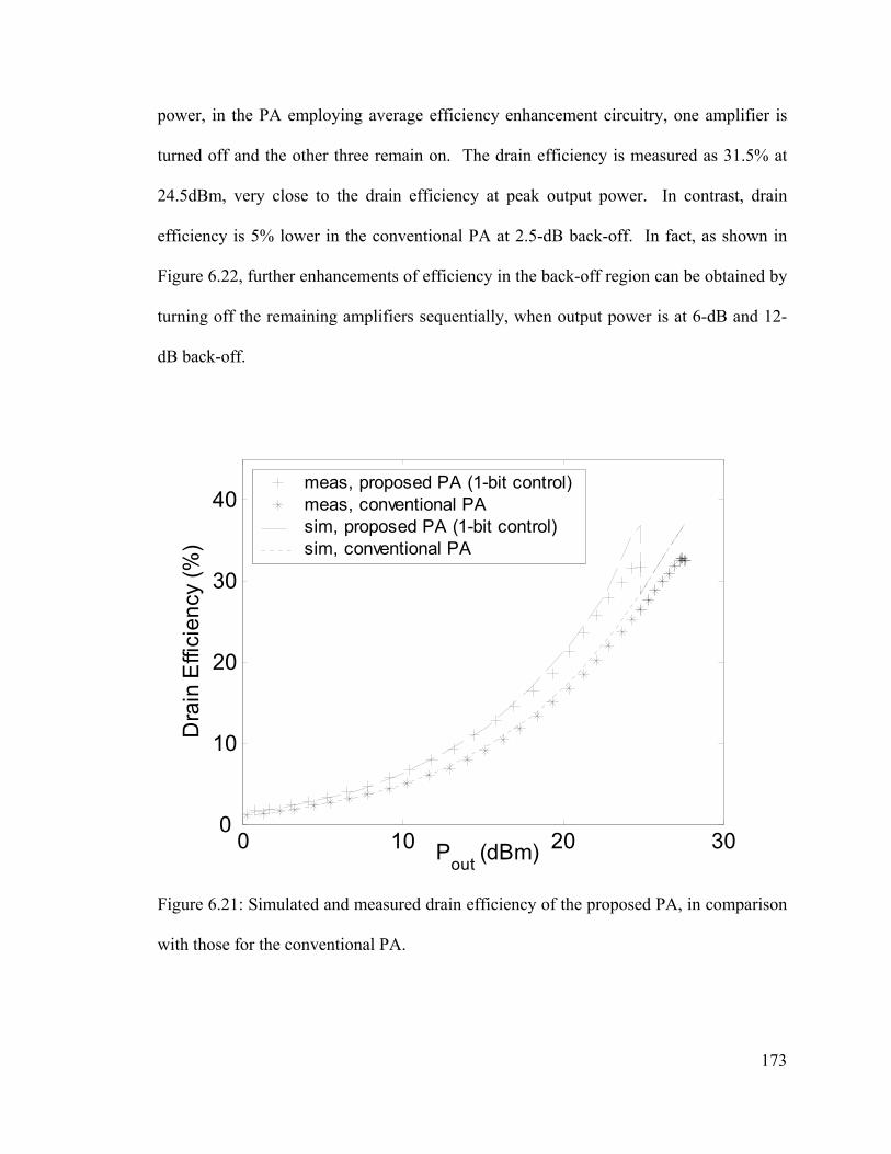
173
power, in the PA employing average efficiency enhancement circuitry, one amplifier is
turned off and the other three remain on. The drain efficiency is measured as 31.5% at
24.5dBm, very close to the drain efficiency at peak output power. In contrast, drain
efficiency is 5% lower in the conventional PA at 2.5-dB back-off. In fact, as shown in
Figure 6.22, further enhancements of efficiency in the back-off region can be obtained by
turning off the remaining amplifiers sequentially, when output power is at 6-dB and 12-
dB back-off.
0 10 20 300
10
20
30
40
Pout (dBm)
Dra
in E
ffici
ency
(%)
meas, proposed PA (1-bit control)meas, conventional PAsim, proposed PA (1-bit control)sim, conventional PA
Figure 6.21: Simulated and measured drain efficiency of the proposed PA, in comparison
with those for the conventional PA.
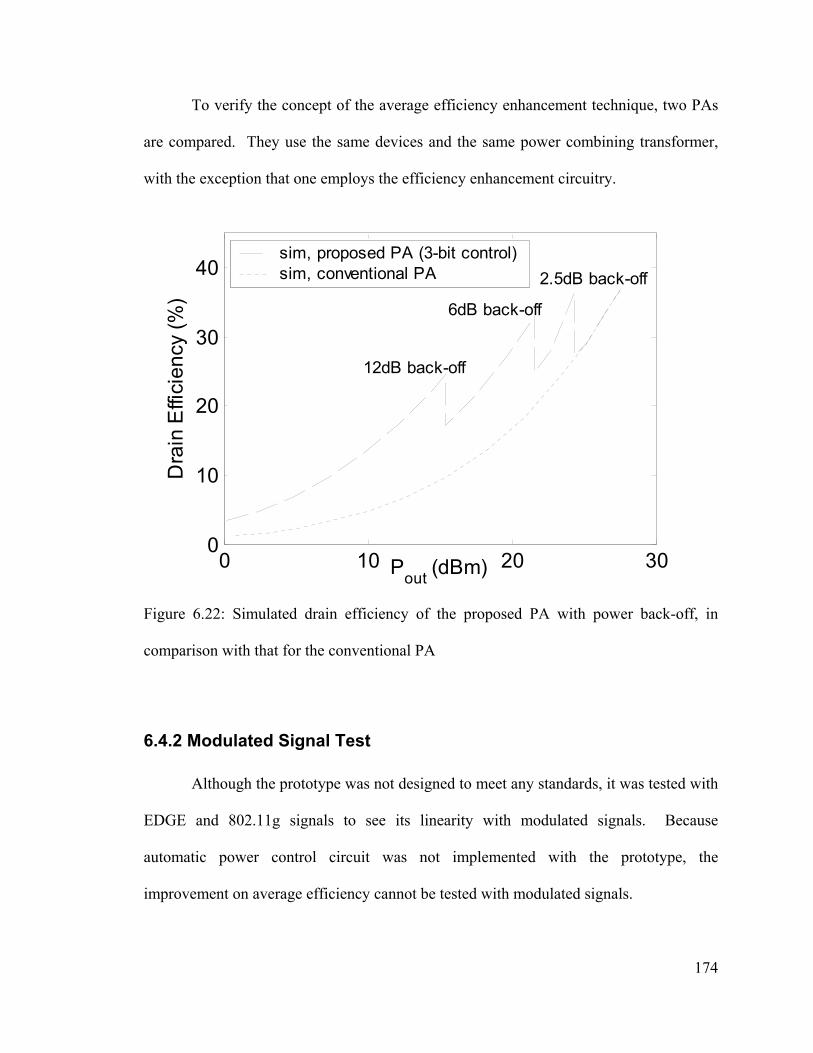
174
To verify the concept of the average efficiency enhancement technique, two PAs
are compared. They use the same devices and the same power combining transformer,
with the exception that one employs the efficiency enhancement circuitry.
0 10 20 300
10
20
30
40
Pout (dBm)
Dra
in E
ffici
ency
(%)
sim, proposed PA (3-bit control)sim, conventional PA
12dB back-off
6dB back-off
2.5dB back-off
Figure 6.22: Simulated drain efficiency of the proposed PA with power back-off, in
comparison with that for the conventional PA
6.4.2 Modulated Signal Test
Although the prototype was not designed to meet any standards, it was tested with
EDGE and 802.11g signals to see its linearity with modulated signals. Because
automatic power control circuit was not implemented with the prototype, the
improvement on average efficiency cannot be tested with modulated signals.
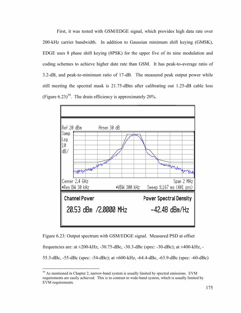
175
First, it was tested with GSM/EDGE signal, which provides high data rate over
200-kHz carrier bandwidth. In addition to Gaussian minimum shift keying (GMSK),
EDGE uses 8 phase shift keying (8PSK) for the upper five of its nine modulation and
coding schemes to achieve higher date rate than GSM. It has peak-to-average ratio of
3.2-dB, and peak-to-minimum ratio of 17-dB. The measured peak output power while
still meeting the spectral mask is 21.75-dBm after calibrating out 1.25-dB cable loss
(Figure 6.23)59. The drain efficiency is approximately 20%.
Figure 6.23: Output spectrum with GSM/EDGE signal. Measured PSD at offset
frequencies are: at ±200-kHz, -30.75-dBc, -30.3-dBc (spec: -30-dBc); at ±400-kHz, -
55.3-dBc, -55-dBc (spec: -54-dBc); at ±600-kHz, -64.4-dBc, -63.9-dBc (spec: -60-dBc)
59 As mentioned in Chapter 2, narrow-band system is usually limited by spectral emissions. EVM requirements are easily achieved. This is in contrast to wide-band system, which is usually limited by EVM requirements.
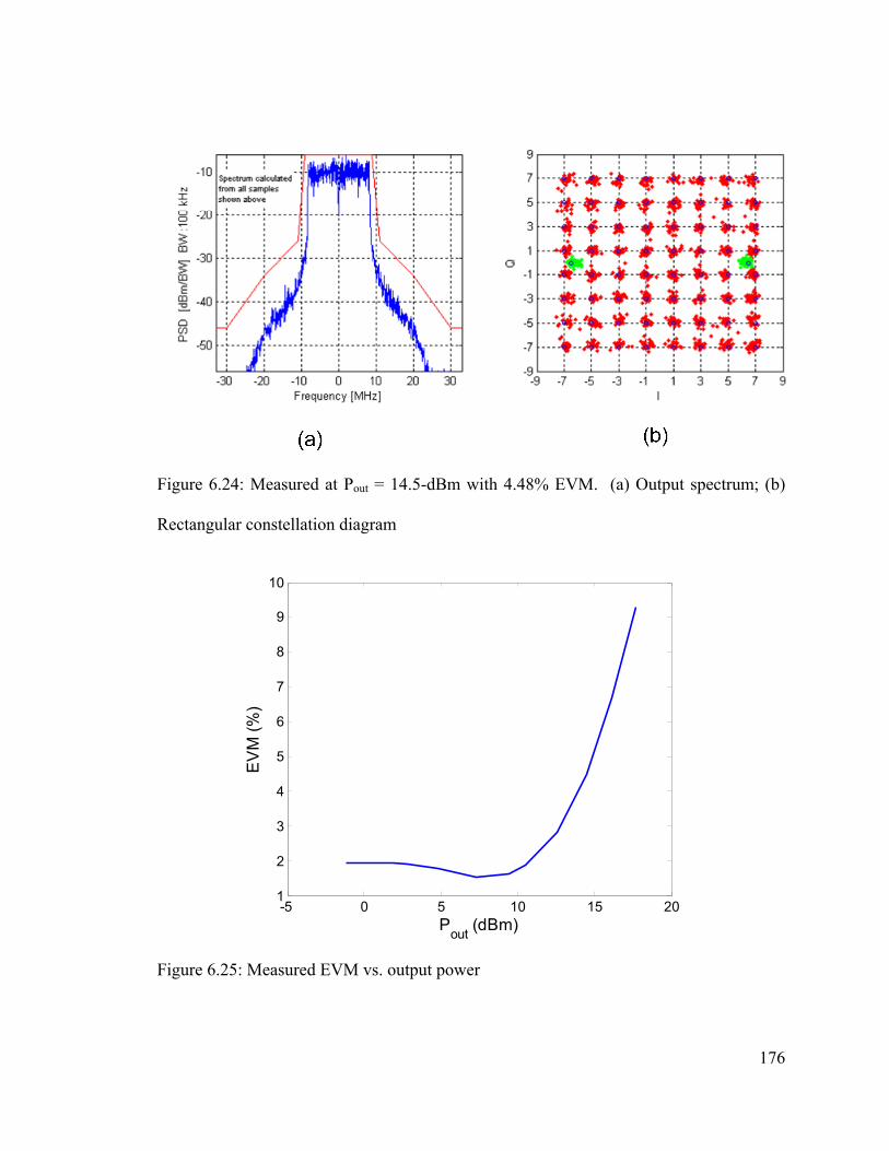
176
Figure 6.24: Measured at Pout = 14.5-dBm with 4.48% EVM. (a) Output spectrum; (b)
Rectangular constellation diagram
-5 0 5 10 15 201
2
3
4
5
6
7
8
9
10
Pout (dBm)
EV
M (%
)
Figure 6.25: Measured EVM vs. output power

177
6.5 Summary
In this chapter, the design approach of the power amplifier with average
efficiency enhancement is first described. The prototype was implemented using the
design methodology in a 0.13-µm CMOS process. The measurements prove the average
efficiency enhancement technique, and the effectiveness of the design methodology.
Tests with modulated signals show that this amplifier is linear to be used in state-of-the-
art wireless communication systems.
6.6 References
[6.1] C. Fager, J.C. Pedro, N.B. de Carvalho, H. FZirath, F. Fortes, M.J. Rosario, “ A
comprehensive analysis of IMD behavior in RF CMOS power amplifiers”, IEEE J. Solid-
State Circuits, vol. 39, no. 1, pp. 24-24, January 2004
[6.2] C. Fager, J.C. Pedro, N.B. de Carvalho, H. FZirath, “Prediction of IMD in LDMOS
transistor amplifiers using a new large-signal model”, IEEE Trans. Microwave Theory
Tech., vol. 50, no. 12, pp. 2834-2842, December 2002
[6.3] D.R. Webster, G. Ataei, and D.G. Haigh, “Low Distortion MMIC PowerAmplifier
Using a New Form of Derivative Superposition”, IEEE Transactions on MTT, vol. 49, no.
2, pp. 328-332, February 2001
[6.4] J. Kang, A. Hajimiri, and B. Kim, “A Single-Chip Linear CMOS Power Amplifier
for 2.4GHz WLAN,” IEEE ISSCC Digest of Technical Papers, pp. 208-209, February
2006
178
[6.5] H. Hayashi, M. Nakatsugawa, M. Muraguchi, “Quasi-linear amplification using
self-phase distortion compensation technique”, IEEE Transactions on MTT, vol. 43, no.
11, pp. 2557-2564, November 1995
[6.6] R.G. Freitag, S.H. Lee, D.M. Krafcsik, D.E. Dawson, J.E. Degenford, “Stability and
improved circuit modeling considerations for high power MMIC amplifiers”, Digest. of
IEEE Micro. and Milli.-Wave Monolithic Circuits Symposium, 1998
[6.7] S. Jeon, A. Suarez, D.B. Rutledge, “Global stability analysis and stabilization of a
class-E/F amplifier with a distributed active transformer”, IEEE Transactions on MTT,
vol. 53, no. 12, pp. 3712-3722, December 2005

179
Chapter 7. Conclusion
7.1 Thesis summary
7.2 Possible future directions
7.1 Thesis Summary
Explosive growth in wireless communication market has led to consumer demand
for low-cost, small form factor, low power terminals. It has been proven in practice that
high level of integration is the most effective way to provide such a solution. The VLSI
capabilities of CMOS make itself a well-suited vehicle for high integration. Although it
was certainly a non-trivial task to realize system-on-chip (SoC), engineers from industry
together with researches from universities have figured out ways to integrate almost an
entire system on a single chip. Yet there is still one piece missing on the integration chart,
the power amplifiers.
Two major hurdles associated with the design of fully integrated CMOS power
amplifiers are low transistor breakdown voltage/high threshold voltage, and high loss
impedance transformation network consisting of lossy on-chip passives. To overcome
those two hurdles, highly efficient power combining can be used to generate enough
power with good overall efficiency.
Besides integration, there is another serious issue associated with PA design
which is inherent to conventional PA. It is well known that a PA can only achieve
maximum efficiency at peak output power. As output power decreases, efficiency drops
rapidly. However, the need to conserve battery power and to mitigate interference to
180
other users necessitates the transmission of power levels well below the peak output
power of the transmitter. Moreover, since spectrum is a scarce commodity, modern
transmitters for wireless communications employ spectrally efficient digital modulations
with high peak-to-average ratio. Because of these reasons, the PA transmits much lower
than peak output power under typical operating conditions.
This thesis started with an overview of the developments in the field, examined
several important characteristics of a power amplifier, and compared prevalent
technologies for RF power amplifiers, especially CMOS technologies. In Chapter 4, after
presenting various power combining approaches, a simple yet elegant power combining
transformer was proposed as a means to enable CMOS integration and improve average
efficiency simultaneously. The design of the proposed transformer was analyzed in
Chapter 5. The CMOS prototype was implemented and tested to verify the concept. The
design methodology and the experimental results were presented in Chapter 6. With
1.2V supply, it transmits linear power up to 24dBm with 25% drain efficiency. When
driven into saturation, it transmits 27dBm peak power with 32% drain efficiency. As one
of the four amplifiers is turned off for 2.5dB power back-off from 27dBm, drain
efficiency is improved from 26.5% to 31.5%, very close to instantaneous drain efficiency
at peak power. To test its linearity, GSM/EDGE and 802.11g OFDM signals were used
as test signals. The measured results demonstrated that the prototype is linear enough to
amplify high peak-to-average modulated signals linearly.
181
7.2 Possible Future Directions
Almost every research contributes something to the understanding of the specific
subject. Meanwhile, it also opens the door to many other new topics. This work is no
exception. While this work demonstrated average efficiency enhancement technique at
power back-off, the automatic power control circuitry was not designed due to time
constraints at the time of tape-out. A natural extension of this work is to include that in
the prototype and verify its effectiveness with high peak-to-average ratio signals. It
should be noted that AM-PM behavior should be carefully studied as individual
amplifiers are turned on/off. For modulated signals with high peak-to-average ratio, the
probability of signals with large envelope is very small, so does the probability to switch
capacitors. Therefore, switched capacitor arrays work at low frequency. Nonetheless,
quantization noise from switching actions needs to be carefully investigated.
A better approach to handle modulation schemes with high peak-to-average ratio
is presented in Chapter 4, the transformer coupled outphasing amplifier. It is another
interesting case to study. Given the fact that DSP is getting more powerful and the cost
overhead is diminishing, outphasing amplifiers is certainly worth investigation. In this
approach, nonlinear amplifiers could be used to achieve linear amplification, which
certainly presents many advantages. With the proposed power combining transformer,
the load is automatically modulated at the power back-off by varying phase modulation.
Therefore, average efficiency is improved.
It was noted that AM-PM becomes more important in modern modulation
schemes which employ multi-carrier for spectral efficiency and robustness. In practice, it
was found that AM-AM characteristic is correlated with odd order terms in a power

182
series expression, while AM-PM characteristic is correlated with even order terms. This
fact will certainly have impacts on the biasing point of a linear power amplifier. More in-
depth study is very necessary to fully understand this point.