57-65ghz cmos power amplifier using transformer-coupling...
TRANSCRIPT

57-65GHz CMOS Power Amplifier Using Transformer-Coupling and
Artificial Dielectric for Compact Design
PA Symposium1/20/09
Tim LaRocca, and Frank Chang

OverviewIntroductionDesign OverviewDifferential Design• Transmission Line Technology• Artificial Dielectric and Output Matching• Differential and Common-Mode Stability
Transformer• Basics• Combine Matching, Bias and Stability Networks
RF PerformanceLayout

60GHz MotivationReleased standards for unlicensed 57-65GHz spectrum:• IEEE 802.15.3c, ECMA, WirelessHD, IEEE 802.11VHT• Very limited success: “Last-mile” efforts, LMDS, 77GHz Automotive,
71-76GHz and 81-86GHz point-to-point • Military (AEHF cross-link) and science applications dominate
New commercial applications• Uncompressed wireless video transfer: “in-room”, Wireless HDMI• Short distance bulk data transfer: “near-field”, <1m
– P2P (Portable-to-Portable), M2M (Machine-to-machine), Proximity Communication, Wireless hard drive backup
Availability of standard digital CMOS process • High ft (>120GHz) for 90nm gate length• Silicon roadmap http://www.itrs.net predicts 37nm ft > 360GHz• Passive element Q’s are reasonable• Do not have to rely on expensive, but high-performance GaAs or InP
Power AmplifierTypical millimeter-wave power amplifiers• Expensive, but high-performance GaAs/InP• Single-ended• Transmission line based with λ/4 structures, such as Lange or
Wilkinson couplers.• Difficult matching impedances, extremely low.
Millimeter-wave CMOS PAs• Limited publications.• Similar architecture to GaAs design; same disadvantages• Low 1.2V supply voltage (knee voltage problematic)• Low ft• Lossy substrate, low-Q passive elements • Single-digit efficiencies
Goals and Achievements• Double-digit efficiencies above 15% and Pout > 12dbm• Compact design: 80% percent reduction from standard design

Schematic
4. Low loss output match network
2. Differential Line with Artificial Dielectric strips
3. No balun
RFout
1. Transformer interstage and input matching
5. Biasing and ground through transformer center tap. Take advantage of virtual grounds.
6. DC block I/O
RFin

Differential Transmission LineCPW (a) and Shield Microstrip (b) are single-ended.GSSG (c) is pseudo-differential• Need 4-port network analyzer• Large Signal testing difficult: magic-T, transitions, amps, etc.• Need off or on-chip balun which is lossy
GS (d)• True differential• Compact , 3dB more power with negligible area increase• Artificial dielectric strips
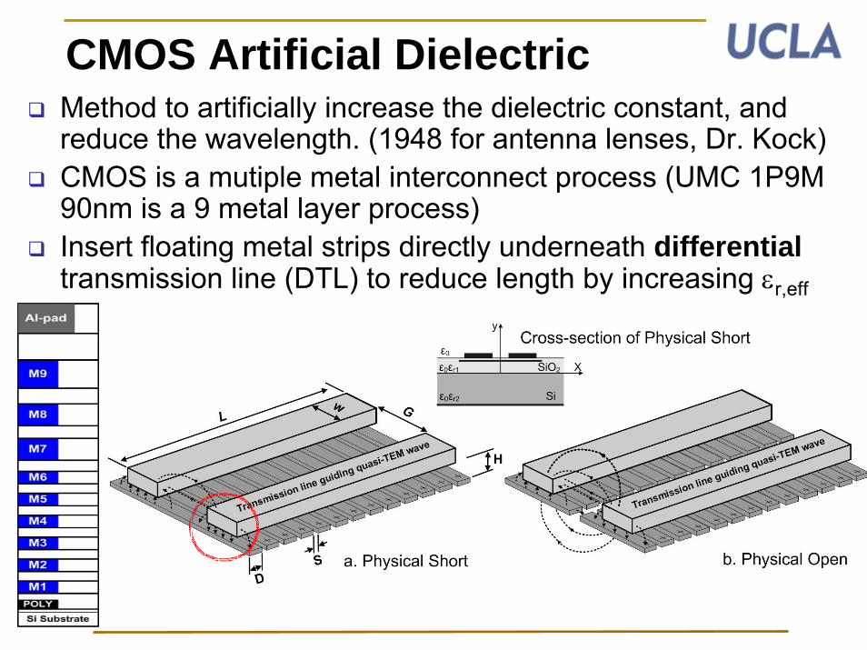
CMOS Artificial DielectricMethod to artificially increase the dielectric constant, and reduce the wavelength. (1948 for antenna lenses, Dr. Kock)CMOS is a mutiple metal interconnect process (UMC 1P9M 90nm is a 9 metal layer process)Insert floating metal strips directly underneath differentialtransmission line (DTL) to reduce length by increasing εr,eff

Phase ShiftLarge phase shift versus “physical short” and “physical open” differential transmission lines.Result is a 6X increase in the effective dielectric constant.
Simulation (SONNET) is solid line and measurement indicated by circles
L 152μm D 3μm
W 24μm S 0.5μm
G 20μm H 0.5μm
Phase of S21 (deg)

AttenuationMeasured attenuation is similarGreater than 2X benefit in α/β when compared with εr,eff
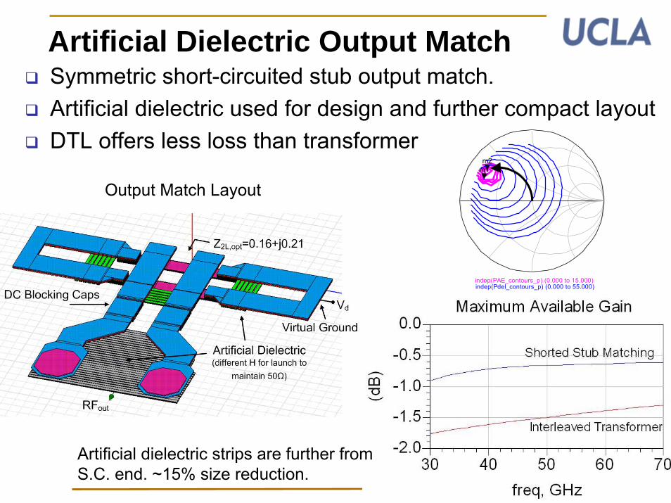
Artificial Dielectric Output MatchSymmetric short-circuited stub output match.Artificial dielectric used for design and further compact layoutDTL offers less loss than transformer
Output Match Layout
indep(PAE_contours_p) (0.000 to 15.000)
m2
indep(Pdel_contours_p) (0.000 to 55.000)
m1
Artificial dielectric strips are further from S.C. end. ~15% size reduction.

Differential and Common-Mode StabilityDifference between GSSG and GS approach.
2112
2222
211
21
dddd
dddddddd SS
SSK
Δ+−−=
2112
2222
211
21
cccc
cccccccc SS
SSK
Δ+−−=
xxxxxxxxxx SSSS 12212211 −=Δ
( )2212211111 21 SSSSS dd +−−=
( )2414231321 21 SSSSS dd +−−=
( )4232413112 21 SSSSS dd +−−=
( )4434433322 21 SSSSS dd +−−=
( )2212211111 21 SSSSS cc +++=
( )2414231321 21 SSSSS cc +++=
( )4232413112 21 SSSSS cc +++=
( )4434433322 21 SSSSS cc +++=
GS Transformer Stability Factor, K
Unstable
GSSG Transformer (Gnd ring)
Stable

DeviceWg = 2um (nf=16,32,64) for Max. Stable Gain.Source and drain fingers are layered from M1-M2.BSIM4 overlaid with RF layout model (Rg, Cext …)Be careful of gate resistance in foundry BSIM models
DrainGate
SourceM1M2
M7
Layout (nf=16)
BSIM4

Transformer ElementTransformer replaces typical matching network. • Inter-stage impedance matching• Biasing through virtual ground taps• Stability (K-factor)• Compact Layout (no lengthy chokes or matching elements)
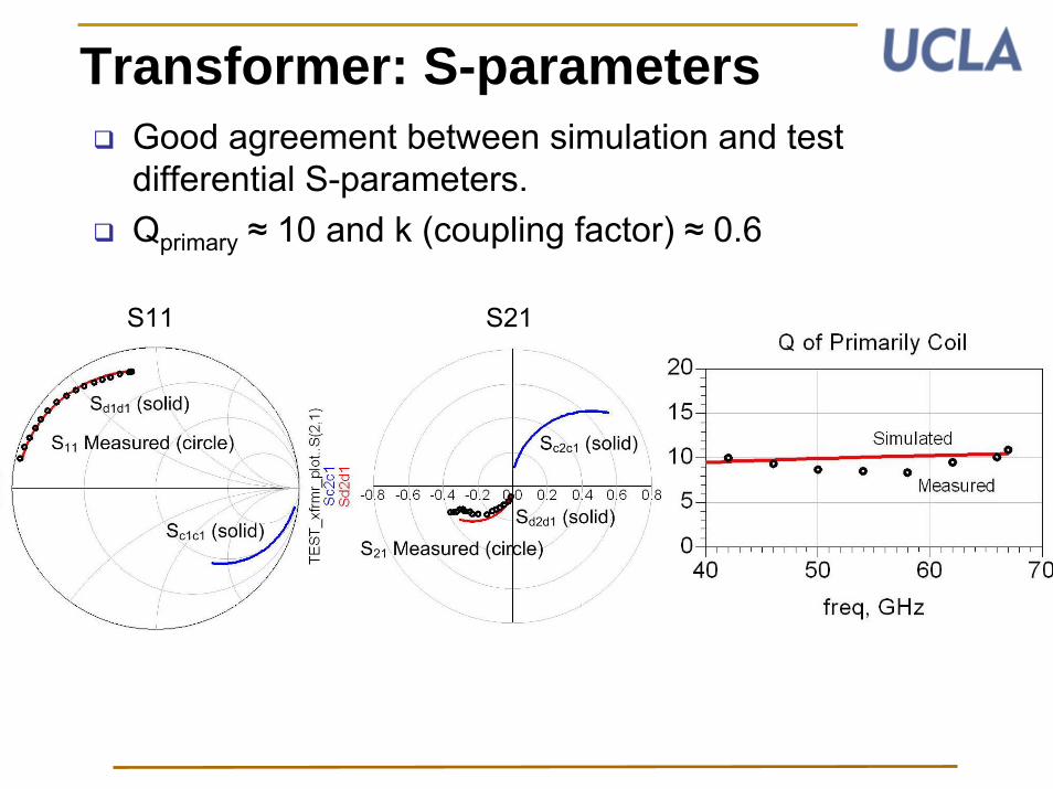
Transformer: S-parametersGood agreement between simulation and test differential S-parameters. Qprimary ≈ 10 and k (coupling factor) ≈ 0.6
S11 S21

Transformer: MatchingSimultaneous impedance matching transformation between the output of the nth-1 stage to the nth stage.
S11(loaded transformer)
Q2 Load Pull CirclesΓOPT,L
S22(loaded transformer)
Q3 Avail. Gain Circles, ΓGa,MAX

Transformer: Matching Path
L1=imag(Z11)/w
R1=imag(Z11)
L2=imag(Z22)/w
R2=imag(Z22)
M=imag(Z12)/w
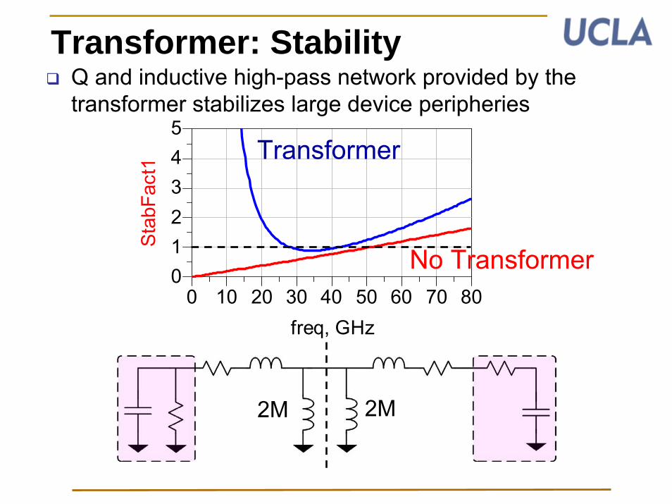
Transformer: Stability
10 20 30 40 50 60 700 80
1234
0
5
freq, GHz
Sta
bFac
t1
2M 2M
Transformer
No Transformer
Q and inductive high-pass network provided by the transformer stabilizes large device peripheries

Transformer RequirmentsWidth determined by power handling capability (RMS current), and low loss [5um and 10um]Turn ratio is determined ~ device periphery ratio (2).Load-pull and S11 determine L1 and L2 (self-inductances)Metal thickness increased by combining M8-M9.Minimum spacing for max. couplingSelf-resonance frequencies >> 60GHz Q1,2 >10-12
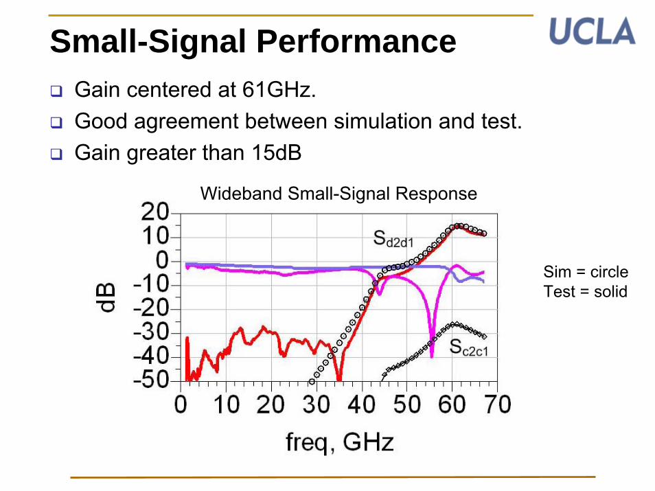
Small-Signal Performance
Wideband Small-Signal Response
Gain centered at 61GHz.Good agreement between simulation and test.Gain greater than 15dB
Sim = circleTest = solid

Swept Power Performance
0
5
10
15
20
25
-15 -10 -5 0 5Input Power (dBm)
Output Power
Gain
PAE
Gain (dB) PAE(%)
Pout(dBm)
Saturated Power above 12dBmEfficiency greater than 19%.
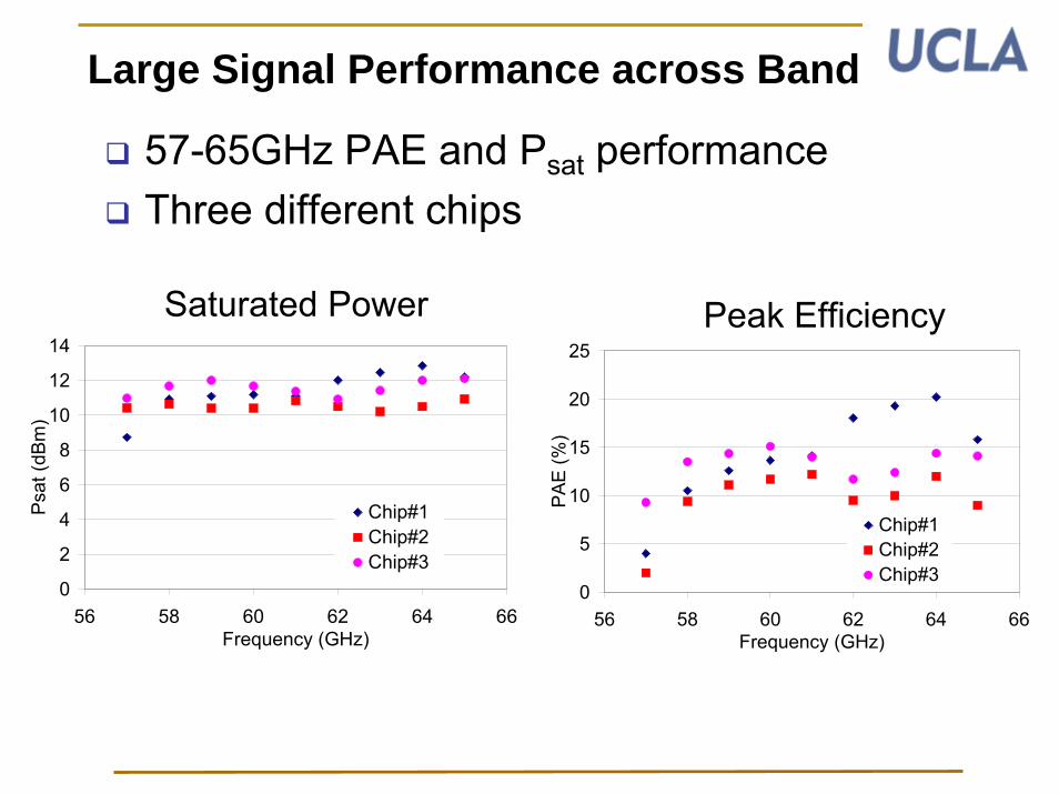
Large Signal Performance across Band
0
2
4
6
8
10
12
14
56 58 60 62 64 66Frequency (GHz)
Psa
t (dB
m)
Chip#1Chip#2Chip#3
0
5
10
15
20
25
56 58 60 62 64 66Frequency (GHz)
PA
E (%
)
Chip#1Chip#2Chip#3
Peak EfficiencySaturated Power
57-65GHz PAE and Psat performanceThree different chips

Comparison to Prior Art
Reference This Work [13] [11] [16] [15]
Technology 90nm 90nm CMOS 90nm 90nm CMOS 90nm CMOS
PSAT (dBm) 12.5 8.4 12.3 10.6 8.4
PAESAT (%) 19.3 7 8.8 ~1 5.8
GainSAT (dB) 11 10.3 2.3 1 8.4
GainLIN (dB) 15 15.2 5.5 8 17
VD (volt) 1.2 0.7 1.0 1.2 na
PDC(mW) 84 89 87 228.6 54
Area (mm2) 0.15 0.18 0.26* 0.97* 0.99*
Highest reported efficiency and power to-date.

LayoutCompact layout with core area 0.15mm2
16.7% the area of original single ended version.• 7-8dB higher gain, and 3.5dBm higher output power
0.3mm
0.5mm
Original
New Design

Test Set-upAgilent 8731E Network Analyzer, SOLT calibrationAgilent 83640A synthesized sweeper, 83557A 50-75GHz source module, NGC GaAs MMIC ampPower measurements calibrated and tested to standard

Conclusion
60GHz differential CMOS transformer-based power amplifier design validated.Highest reported efficiency and saturated power to date.Compact size achievedAcknowledgements• UMC Foundry• Northrop-Grumman Corp.

Process VariationTT,FF,SS corners for BSIM4 Model• F = Low Threshold, high leakage and driving current
20% Capacitive Variation

Atmospheric AbsorptionO2 resonance

RLC Model for Artificial Dielectric
No effect on Inductance Factor 5-6 for capacitance

Electric FieldE-field confined between artificial dielectric strips and DTL (does not shield H-field)

Short-Circuited Stub EffectNo difference between “physical short” and “physical open” S.C. stub elements
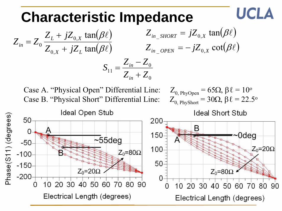
Characteristic Impedance( )( )ll
ββ
tantan
,0
,00
LX
XLin jZZ
jZZZZ
++
=( )lβtan,0_ XSHORTin jZZ =
( )lβcot,0_ XOPENin jZZ −=
0
011 ZZ
ZZSin
in
+−
=
Case A. “Physical Open” Differential Line: Z0, PhyOpen = 65Ω, βℓ = 10o
Case B. “Physical Short” Differential Line: Z0, PhyShort = 30Ω, βℓ = 22.5o

Transformer: Differential ModeExtract differential and common mode S-parameters from electromagnetic simulationMeasurements match Differential Mode Simulation

Effective Dielectric ConstantShort/Open Stub
⎟⎟⎠
⎞⎜⎜⎝
⎛⎟⎟⎠
⎞⎜⎜⎝
⎛=
⎟⎟⎠
⎞⎜⎜⎝
⎛⎟⎟⎠
⎞⎜⎜⎝
⎛=
−
−
o
inshort
o
inopen
ZZimag
ZZimag
1
1
tanh1
coth1
l
l
β
β
2/
⎟⎟⎠
⎞⎜⎜⎝
⎛=
ωβ
εcshop
eff

Q TransformerQ is approximately 10
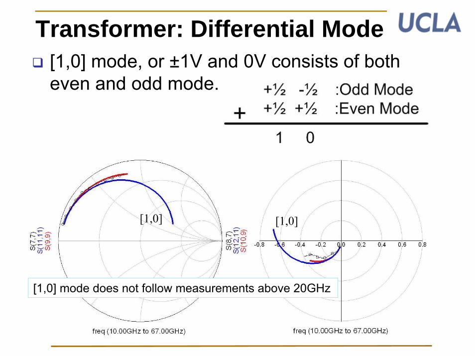
Transformer: Differential Mode[1,0] mode, or ±1V and 0V consists of both even and odd mode.
[1,0] [1,0]
[1,0] mode does not follow measurements above 20GHz
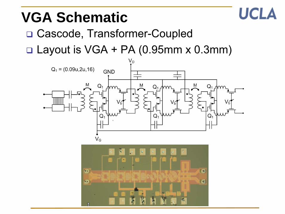
VGA SchematicCascode, Transformer-CoupledLayout is VGA + PA (0.95mm x 0.3mm)
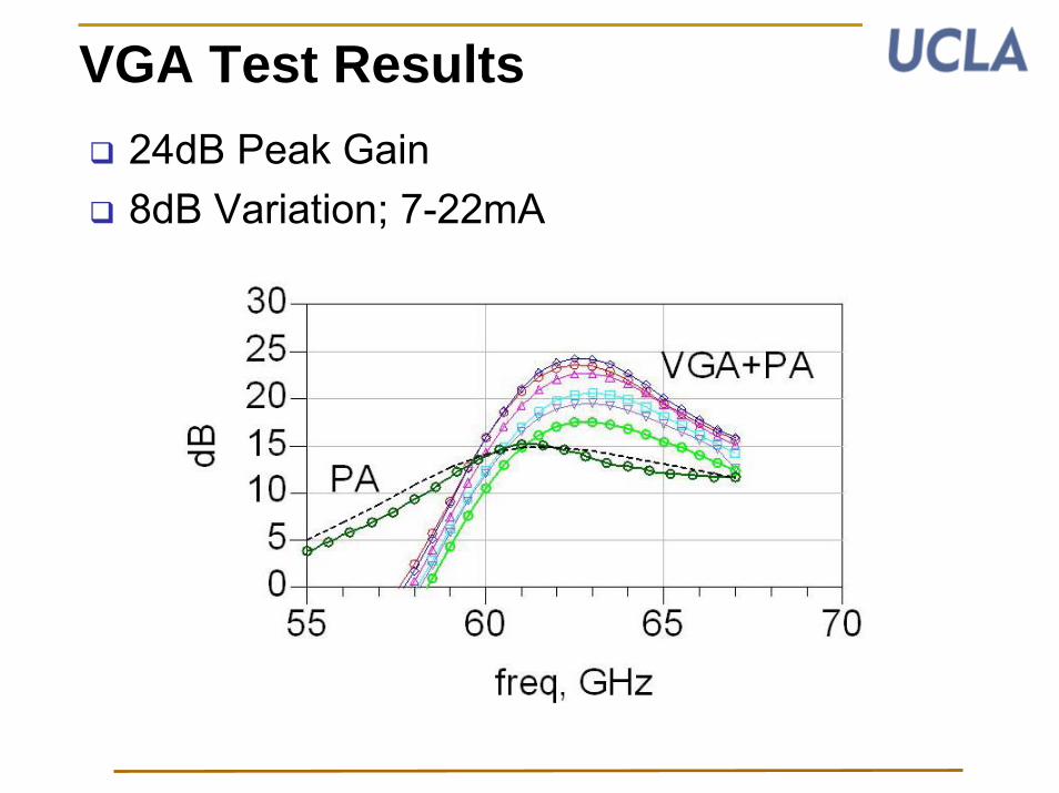
VGA Test Results24dB Peak Gain8dB Variation; 7-22mA
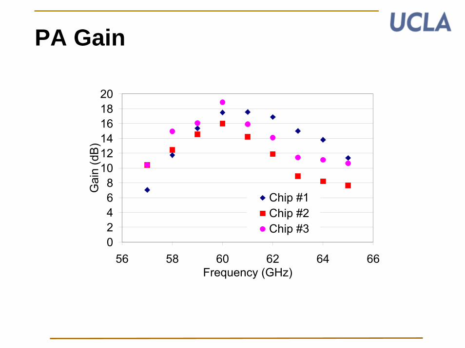
PA Gain
02468
101214161820
56 58 60 62 64 66Frequency (GHz)
Gai
n (d
B)
Chip #1Chip #2Chip #3

GaAs MMIC (ALH382)
PA
-8 -6 -4 -2 0 2 4 6 8 10-10 12
5
10
15
20
25
0
30
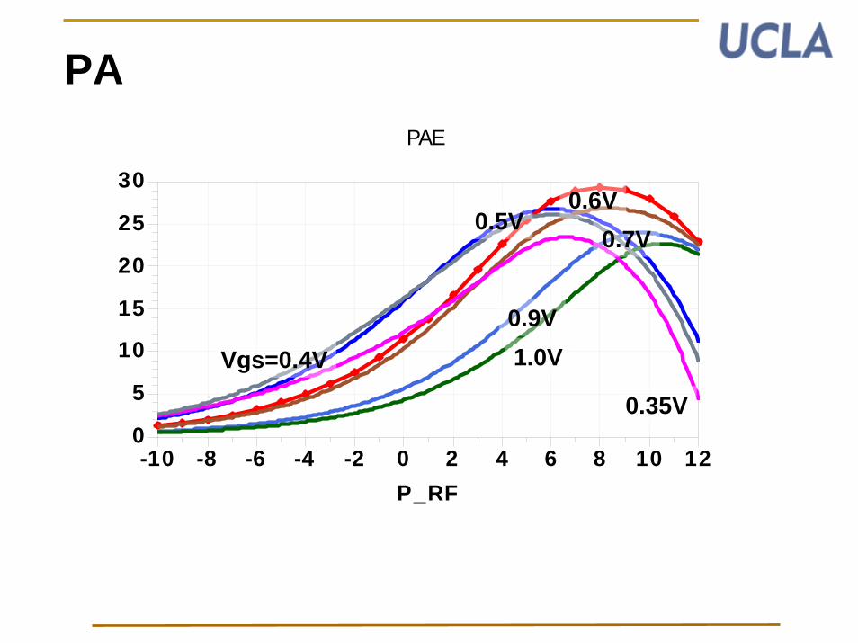
P_RF
PAE
0.35V
1.0V0.9V
0.6V0.7V
Vgs=0.4V
0.5V

PA Output Power
-8 -6 -4 -2 0 2 4 6 8 10-10 12
-5
0
5
10
-10
15
Out
put P
ower
(dB
m)
Input Power (dBm)
Conduction Angle Increase
Vgs=0.35V
1.0V
0.6V
Class B
Class A
Vgs Slope0.35V 0.990.6V 0.850.9V 1.02

PA Test Set-up