monolayer mos nanoribbons as a promising material for both ...davydov/16arab_mos2 for...
TRANSCRIPT

Monolayer MoS2 Nanoribbons as a Promising Material for Bothn-type and p-type Legs in Thermoelectric Generators
A. ARAB,1,2,4 A.V. DAVYDOV,2 D.A. PAPACONSTANTOPOULOS,3
and Q. LI1
1.—Department of Electrical and Computer Engineering, George Mason University, Fairfax, VA,USA. 2.—Material Science and Engineering Laboratory, National Institute of Standard andTechnology, Gaithersburg, MD, USA. 3.—School of Computational Sciences, George MasonUniversity, Fairfax, VA, USA. 4.—e-mail: [email protected]
First-principles calculations have been performed to study the thermoelectricproperties of monolayer MoS2 armchair nanoribbons (ACNRs). The electronicbehavior of nanoribbons is dominated by the presence of edge states that aredependent on the number of zigzag chains across the nanoribbon. In addition,it is found that the phonon thermal conductance of monolayer MoS2 ACNRs issmaller than monolayer films due to phonon edge scattering. This effect ismore pronounced in narrower nanoribbons, which leads to a higher ZT valuecompared to a monolayer MoS2 sheet. The effects of sulfur vacancy and edgeroughness on the thermoelectric properties of MoS2 ACNRs have also beenstudied. We found that edge roughness decreased ZT values compared to thoseof perfect nanoribbons, as its impact on electrical conductance is more severethan on phonon thermal conductance. Sulfur vacancy, however, improved ZTin some subbands. It is shown that ZT values as high as 4 for electron-dopedand 3 for hole-doped nanoribbons can be achieved at T = 500 K. The ability toachieve high ZT values for both p-type and n-type nanoribbons makesmonolayer MoS2 ACNR a promising candidate for future solid-state thermo-electric generators.
Key words: Thermoelectric generation, MoS2 Nanoribbon, seebeckcoefficient, ZT
INTRODUCTION
Atomically thin two-dimensional (2D) materialshave attracted a strong interest since the discoveryof graphene.1 Great strides have been made towardunderstanding graphene’s interesting physical andelectrical properties.2–4 However, the potential useof graphene in electronics applications has beenhindered by the fact that it has zero band gap (Eg) inits pristine form. More recently, another family of2D materials has emerged: transition metaldichalcogenides (TMDCs). Bulks of these materialsare formed by layers vertically stacked and weaklybonded together via van der Waals forces. Thisweak interlayer interaction makes it possible to
obtain monolayers by using scotch tape exfoliation5
or lithium-ion intercalation6 techniques. In contrastto graphene with Eg = 0, some members of theTMDC family have an appropriate band gap formicroelectronic applications. Molybdenum disulfide(MoS2) is one of the most representative andintensively studied 2D TMDCs, in part due to itsthermal stability and natural abundance.7–9 BulkMoS2 is an indirect gap semiconductor10 withEg = 1.2 eV, while monolayer MoS2 is a direct gapsemiconductor11 with Eg = 1.8 eV. The desirableband gap, good carrier mobility (which is close tothose of silicon thin films and graphene nanorib-bons),12 excellent thermal stability, and a smoothsurface free from dangling bonds,13 make MoS2 apromising candidate for electronic and optoelec-tronic applications.14
(Received April 21, 2016; accepted June 2, 2016)
Journal of ELECTRONIC MATERIALS
DOI: 10.1007/s11664-016-4725-9� 2016 The Minerals, Metals & Materials Society

The thermoelectric properties of MoS2 have notbeen as well studied as its electrical properties.15,16
The direct conversion of heat into electricity inthermoelectric materials is considered a solution forusing wasted heat energy sources as renewableenergy supplies, and hence, highly efficient thermo-electric materials and devices have attracted inten-sive interest. Performance of a thermoelectricmaterial in converting heat into electricity can beevaluated by a figure of merit; ZT = GS2T/(je + jph),in which G, S, T, je and jph are the electricalconductance, Seebeck coefficient, absolute tempera-ture, electronic contribution to thermal conduc-tance, and phonon contribution to thermalconductance, respectively. It is desirable to have ahigh electrical conductance and Seebeck coefficientand low thermal conductance to achieve a high ZTvalue. For conventional thermoelectric materials,e.g., PbTe17 and Bi2Te3-based alloys,18 ZT values ofaround 2.4 at T = 900 K were achieved. Furtherincrease of ZT in these materials proved to be achallenge since the parameters that affect ZT aregenerally coupled with each other. Enhancement toone of them may degrade the other and the overalleffect on ZT will neutralize. The situation did notchange much until higher ZT values were shown inthe low-dimensional19,20 and nanostructured ther-moelectric materials,21 whereas their Seebeck coef-ficients were enhanced by quantum confinementand their thermal conductance were decreased byincreasing phonon boundary scattering.22 Thermalconductivity can be further decreased by deliber-ately introducing surface roughness23 and defects inmaterials.24
The high Seebeck coefficient of 600 lV/K at roomtemperature25 reported for bulk MoS2 is higherthan that seen in most good thermoelectric materi-als. It was also reported that the Seebeck coefficientof MoS2 can be tuned as high as 105 lV/K byimposing a gate electric field.26 In addition, lowthermal conductivity was also reported for MoS2
thin films.27,28 Despite the reported high Seebeckcoefficient and low thermal conductivity, bulk MoS2
was predicted to have a low ZT value29 of 0.1 at700 K that could be attributed to its poor conduc-tivity.25,30,31 High pressure was used in an attemptto tune interlayer interactions of bulk MoS2, and itsZT increased to 0.65 over a wide range of temper-ature and pressure.32
In addition, anisotropy in the thermal conduc-tance33 and ZT34 is reported in armchair and zigzagdirections. In our previous study, we calculated ZTvalues of the 2D monolayer and few-layer MoS2
sheets in both armchair and zigzag directions in adensity functional theory (DFT) framework.34 Weshowed that by increasing the number of layers, theZT value decreased and also higher ZT values couldbe achieved in armchair as compared to zigzagMoS2.34 The highest ZT value was 1.2 for p-typearmchair MoS2 monolayers, which is in good
agreement with a previous report.35 This repre-sented a large ZT boost from bulk MoS2.
By taking advantage of the higher boundaryscattering, and hence lower thermal conductance,of one-dimensional (1D) nanoribbons in comparisonwith 2D sheets, higher ZT values can be achieved.Recently, MoS2 nanoribbons with widths varyingfrom tens of nanometers to hundreds of nanometershave been synthesized by electrochemical andchemical methods.36,37 More recently, nanoribbonswith uniform widths of just 0.35 nm have beenformed in MoS2 sheets under electron irradiation.38
One of the most important obstacles in achievingdevices based on low-dimensional MoS2 is to developa method leading to a large-scale and uniformgrowth. There have been many efforts toward thisgoal using various chemical vapor deposition (CVD)methods such as sulfurization of metal or metalcompounds39,40 or CVD based on solid precursors(such as MoO3 or MoCl5).41,42 In all these cases,uniformity of the grown films has been a challenge.More recently, a successful uniform monolayergrowth of MoS2 has been reported using the metalorganic CVD (MOCVD) method.43 This achievementmakes it more important than before to investigatethe thermoelectric properties of 1D monolayer MoS2
nanoribbons. Recently, the thermoelectric proper-ties of MoS2 nanoribbons have been studied in aDFT framework with relaxation time approxima-tion.44 Authors have reported a high value of ZT � 3requiring a small amount of Fermi-level shift. Basedon a ballistic transport regime, in which no scatter-ing mechanism has been considered, it has beenshown in this study that it is indeed possible toobtain a high value of ZT � 3–4 but with a muchhigher Fermi-level shift. We have also consideredthe effect of nanoribbon defects, such as edgeroughness and sulfur vacancies, on its thermoelec-tric behavior.
COMPUTATIONAL APPROACH
The computational model is based on DFT using anon-equilibrium Green’s function (NEGF) method45
implemented in the QuantumWise ATK softwarepackage. aPrior to performing each electronic andphonon calculation, the super-cells have beenrelaxed to maximum force and stress of 0.05 eV/Aand 0.05 eV/A3, respectively. The generalized gra-dient approximation (GGA) exchange correlation,double-zeta polarized (DZP) basis set, mesh cut-offenergy of 75 Ha and 10 9 10 9 10 k-point grid isused for relaxation calculations. A large vacuumspacing of at least 20 A is added in each side of thenanoribbons to hinder the effect of periodic images.The Landauer-Buttiker46 formula is used to calcu-late transport coefficients of the system fromGreen’s function. This formalism is correct in theabsence of inelastic scattering and phase-changingmechanisms. In the DFT calculations, Monkhorst–
Arab, Davydov, Papaconstantopoulos, and Li

Pack k-grid47 of 1 9 1 9 100 and DZP basis set withdensity mesh cut-off of 10 Ha is used for super cellswithin localized density approximation (LDA).
For the electronic transport calculation, the struc-ture is comprised of a channel region and twoelectrodes. These electrodes are semi-infinite,defect-free MoS2 nanoribbons with periodic bound-ary condition. The retarded Green’s function ofchannel is calculated as48
G Eð Þ ¼ Eþ i0þð ÞI �H � RL � RR½ ��1 ð1Þwhere H is the channel Hamiltonian matrix andRL(R) is the self-energy due to the semi-infiniteleft(right) electrode. Electronic transmission perspin through the channel region is obtained as
Te Eð Þ ¼ tr CL Eð Þ �G Eð Þ � CR Eð Þ �Gþ Eð Þ½ � ð2Þ
in which CL(R)(E) = �2 Im(RL(R)) is the broadeningfunction of the left(right) electrode and G+is theadvanced Green’s function.
Carrier transport properties are calculated by aballistic transport approach under a linear responseregime. The electrical current I in this regime isgiven by46
I ¼ 2q
h
ZdE � Te Eð Þ � fL E; lLð Þ � fR E; lRð Þf g ð3Þ
in which the factor of two counts for spin degener-acy, q is the electrical charge, h is the Planck’sconstant, Te(E) is the electronic transmission spec-trum, lL(R) is the chemical potential of the left(right)electrode, and fL(R)(E, lL(R)) is the Fermi distribu-tion of the left(right) electrode. The Fermi distribu-tion function depends on both the chemical potentialand the temperature. In the linear response regime,it is assumed that the system is biased with aninfinitesimal voltage drop and temperature gradi-ent. As a result, Eq. 3 will be reduced to
I ¼ 2q
hDl
ZdE � T Eð Þ � @f
@lþ 2q
hDT
ZdE � T Eð Þ� @f
@T
ð4Þwhere Dl and DT are infinitesimally small. We areinterested in the electrical response of monolayerMoS2 ACNRs to the pure temperature gradient, i.e.there is no voltage bias applied to the electrodes inour simulations, and therefore, Dl = 0 and Eq. 4will reduce to
I ¼ 2q
hDT
ZdE � T Eð Þ� @f
@Tð5Þ
The electrical conductance (G), Seebeck coeffi-cient (S), and electronic contribution to thermalconductance (je) are calculated by using electronictransmission spectrum as follows
G ¼ q2L0 ð6Þ
S ¼ L1
qTL0ð7Þ
je ¼ 1
TL2 �
L21
L0
� �ð8Þ
where Ln is expressed as
Ln ¼ 2
h
ZdE � T Eð Þ � � @f E; lð Þ
@E
� �� E� lð Þn ð9Þ
Phonon calculations are performed based on param-eterization of the Stillinger–Weber potential49 forMoS2
28 as implemented in the QuantumWise ATKpackage. Phonon thermal conductance (jph) can becalculated as
jph ¼ limDT!0
1h
R10
dE � Tph Eð Þ � E � B E;TLð Þ � B E;TRð Þf g
DTð10Þ
where Tph(E) is the phonon transmission spectrum,B(E, TL(R)) is the Bose–Einstein distribution of theleft(right) electrode, TL(R) is the temperature of theleft(right) electrode, and E is the energy of trans-mitted phonons. In the linear response regime,temperature bias on the electrodes is infinitesimallysmall. As a result, Eq. (10) becomes
jph ¼ 1
h
Z1
0
dE � Tph Eð Þ � E � � @B E;Tð Þ@T
� �ð11Þ
The thermoelectric figure of merit can be readilyobtained using these parameters as
ZT ¼ GS2T
je þ jphð12Þ
It is worth mentioning that the phonon calculationsin this paper are performed in the absence of anyphonon decaying mechanisms. As a result, thesecalculations set the upper limit for the phononthermal conductance. In real situations, however,there would be a few mechanisms such as scatteringcenters, crystal imperfectness, surface roughness,etc., which tend to suppress phonon conduction;therefore, ZT values calculated in this study areminimum values of what actually can be achievedby monolayer MoS2 ACNRs.
RESULTS AND DISCUSSION
The atomic structure of the monolayer MoS2
ACNRs, as shown in Fig. 1, can be considered asmonolayer MoS2 tailored along the armchair direc-tion. Nanoribbons with various widths can beidentified by a number of zigzag chains across theACNR, as illustrated in Fig. 1, and are labeled as N-ACNR. In this study, we focus on eight different
Monolayer MoS2 Nanoribbons as a Promising Material for Both n-type and p-type Legsin Thermoelectric Generators
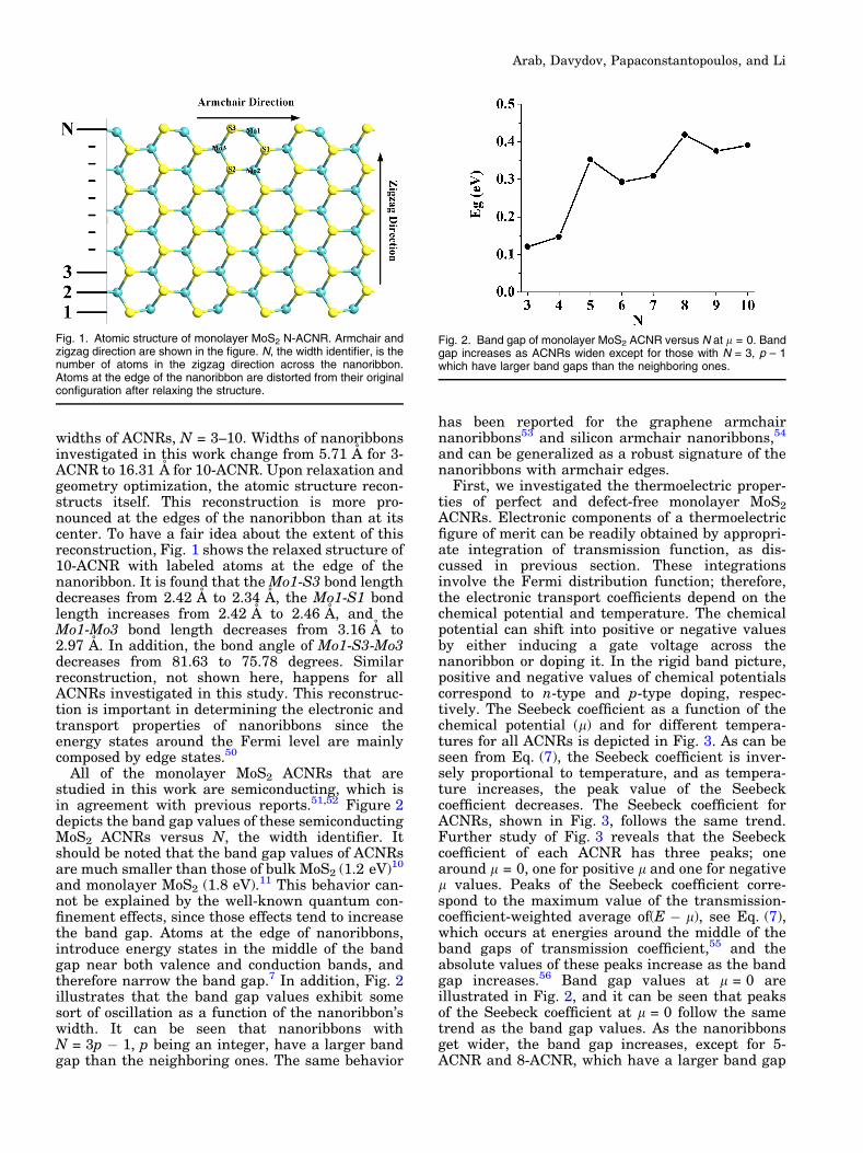
widths of ACNRs, N = 3–10. Widths of nanoribbonsinvestigated in this work change from 5.71 A for 3-ACNR to 16.31 A for 10-ACNR. Upon relaxation andgeometry optimization, the atomic structure recon-structs itself. This reconstruction is more pro-nounced at the edges of the nanoribbon than at itscenter. To have a fair idea about the extent of thisreconstruction, Fig. 1 shows the relaxed structure of10-ACNR with labeled atoms at the edge of thenanoribbon. It is found that the Mo1-S3 bond lengthdecreases from 2.42 A to 2.34 A, the Mo1-S1 bondlength increases from 2.42 A to 2.46 A, and theMo1-Mo3 bond length decreases from 3.16 A to2.97 A. In addition, the bond angle of Mo1-S3-Mo3decreases from 81.63 to 75.78 degrees. Similarreconstruction, not shown here, happens for allACNRs investigated in this study. This reconstruc-tion is important in determining the electronic andtransport properties of nanoribbons since theenergy states around the Fermi level are mainlycomposed by edge states.50
All of the monolayer MoS2 ACNRs that arestudied in this work are semiconducting, which isin agreement with previous reports.51,52 Figure 2depicts the band gap values of these semiconductingMoS2 ACNRs versus N, the width identifier. Itshould be noted that the band gap values of ACNRsare much smaller than those of bulk MoS2 (1.2 eV)10
and monolayer MoS2 (1.8 eV).11 This behavior can-not be explained by the well-known quantum con-finement effects, since those effects tend to increasethe band gap. Atoms at the edge of nanoribbons,introduce energy states in the middle of the bandgap near both valence and conduction bands, andtherefore narrow the band gap.7 In addition, Fig. 2illustrates that the band gap values exhibit somesort of oscillation as a function of the nanoribbon’swidth. It can be seen that nanoribbons withN = 3p � 1, p being an integer, have a larger bandgap than the neighboring ones. The same behavior
has been reported for the graphene armchairnanoribbons53 and silicon armchair nanoribbons,54
and can be generalized as a robust signature of thenanoribbons with armchair edges.
First, we investigated the thermoelectric proper-ties of perfect and defect-free monolayer MoS2
ACNRs. Electronic components of a thermoelectricfigure of merit can be readily obtained by appropri-ate integration of transmission function, as dis-cussed in previous section. These integrationsinvolve the Fermi distribution function; therefore,the electronic transport coefficients depend on thechemical potential and temperature. The chemicalpotential can shift into positive or negative valuesby either inducing a gate voltage across thenanoribbon or doping it. In the rigid band picture,positive and negative values of chemical potentialscorrespond to n-type and p-type doping, respec-tively. The Seebeck coefficient as a function of thechemical potential (l) and for different tempera-tures for all ACNRs is depicted in Fig. 3. As can beseen from Eq. (7), the Seebeck coefficient is inver-sely proportional to temperature, and as tempera-ture increases, the peak value of the Seebeckcoefficient decreases. The Seebeck coefficient forACNRs, shown in Fig. 3, follows the same trend.Further study of Fig. 3 reveals that the Seebeckcoefficient of each ACNR has three peaks; onearound l = 0, one for positive l and one for negativel values. Peaks of the Seebeck coefficient corre-spond to the maximum value of the transmission-coefficient-weighted average of(E � l), see Eq. (7),which occurs at energies around the middle of theband gaps of transmission coefficient,55 and theabsolute values of these peaks increase as the bandgap increases.56 Band gap values at l = 0 areillustrated in Fig. 2, and it can be seen that peaksof the Seebeck coefficient at l = 0 follow the sametrend as the band gap values. As the nanoribbonsget wider, the band gap increases, except for 5-ACNR and 8-ACNR, which have a larger band gap
Fig. 1. Atomic structure of monolayer MoS2 N-ACNR. Armchair andzigzag direction are shown in the figure. N, the width identifier, is thenumber of atoms in the zigzag direction across the nanoribbon.Atoms at the edge of the nanoribbon are distorted from their originalconfiguration after relaxing the structure.
Fig. 2. Band gap of monolayer MoS2 ACNR versus N at l = 0. Bandgap increases as ACNRs widen except for those with N = 3, p – 1which have larger band gaps than the neighboring ones.
Arab, Davydov, Papaconstantopoulos, and Li

than the neighboring nanoribbons, and hence theSeebeck peaks around l = 0 also increase. Trans-mission spectra of three ACNRs that exhibit dis-tinctive Seebeck coefficient profiles are depicted inFig. 4 in order to further clarify how the band gapvalues affect the Seebeck coefficient profile. Thetransmission spectrum of each ACNR has threeband gaps. There is a band gap at l = 0 (center-gap),a band gap at positive l values (positive-l gap), anda band gap at negative l values (negative-l gap).One of these gaps is wider than the other two in thetransmission spectrum of each ACNR. As is depictedin Fig. 4, the positive-l gap, negative-l gap, andcenter gap are the widest gaps for 3-ACNR, 4-ACNR, and 10-ACNR, respectively. The Seebeckcoefficient profiles, illustrated in Fig. 3, follow thesame trend, as their peak values are higher where
Fig. 3. Seebeck coefficient of N-ACNRs for N = 3–10 versus the chemical potential for different temperatures in (a) through (h).
Fig. 4. Transmission spectra for N-ACNRs with N = 3, 4, and 10.Each transmission spectrum comprised of three band gaps. For 10-ACNR, the band gap at l = 0 is larger than the other two. For 3-ACNR and 4-ACNR, however, the band gap for n-type and p-type (inrigid band picture) is the largest, respectively.
Monolayer MoS2 Nanoribbons as a Promising Material for Both n-type and p-type Legsin Thermoelectric Generators

the gap is wider in their corresponding transmissionspectra.
Electrical conductance (G) and electronic thermalconductance (je) are the other two electronic trans-port coefficients that can be obtained from thetransmission spectra. These two transport coeffi-cients for 3-ACNR, 4-ACNR, and 10-ACNR areillustrated in Fig. 5. Panels (a) and (b) show G andje at room temperature, respectively. The profilesfor both of these transport coefficients follow thesame trend as their corresponding transmissionspectra versus chemical potential. As the chemicalpotential moves into conduction or valence bands,there are more carriers to be conducted thermallyand electrically; therefore, both G and je increase.Also, when the chemical potential enters the bandgaps, both G and je are supposed to be zero.However, this is not the case when the chemicalpotential enters small band gaps in transmissionspectra. As is depicted for 3-ACNR and 4-ACNR inFig. 5, the center gaps are in the order of 5 KB T andthe Fermi distribution function excites some of thetransmission channels even when the chemicalpotential is well inside these band gaps. As a result,when the chemical potential moves into these smallband gaps, electrical and thermal conductancedecreases but does not drop to zero. Similar behav-ior can be seen at the positive-l gap and negative-lgap for 10-ACNR. Panels (c) and (d) of Fig. 5
illustrate G and je of 10-ACNR versus the chemicalpotential for different temperatures. It can be seenfrom panel (c) that for the center gap, electricalconductance does not change very much as thetemperature increases, while at the positive-l gapand negative-l gap, it changes more significantly.This behavior is due to broadening of the Fermidistribution function. For higher temperatures,Fermi distribution is broader and excites morestates in neighboring bands than at lower temper-atures. This effect is more pronounced for smallergaps as compared to larger gaps. The electronicthermal conductance of 10-ACNR for different tem-peratures is illustrated in panel (d) of Fig. 5. Athigher temperatures more carriers will be con-ducted thermally, and electronic thermal conduc-tance increases.
Phonon thermal conductance (jph) has beenobtained by parametrization of the Stillinger–We-ber potential for MoS2. In contrast to je, jph is notaffected by shifting the chemical potential and isconstant as l changes. Phonon thermal conductanceincreases as temperature increases, as is shown inpanel (a) of Fig. 6 (not shown for all ACNRs). Inaddition, it can be noted that the rate at which jph
increases versus temperature is higher for widernanoribbons as compared to narrower nanoribbons.Moreover, jph at room temperature for all ACNRs isillustrated in panel (b) of Fig. 6. As nanoribbons get
Fig. 5. Electrical conductance and electronic thermal conductance for N-ACNRs with N = 3, 4, and 10 versus chemical potential in panels (a)and (b), respectively. Electrical conductance and electronic thermal conductance of 10-ACNR versus chemical potential for different tempera-tures are illustrated in (c) and (d), respectively.
Arab, Davydov, Papaconstantopoulos, and Li

wider, jph increases. In narrower nanoribbons,there are fewer channels to conduct heat byphonons and the effect of edge phonon scatteringis more profound as compared to wider nanoribbons.As nanoribbons widen, there are more availablechannels for phonons to conduct heat and the effectof boundary scattering decreases.57
Now that all the parameters have been computed,
the thermoelectric figure of merit, ZT ¼ GS2
jeþjphT, can
readily be obtained. ZT values of all monolayerMoS2 ACNRs as a function of the chemical potentialposition and for various temperatures have beenillustrated in Fig. 7. The Seebeck coefficient, as canbe seen from Fig. 3, reaches its maximum value atenergies around ± KBT of the middle of each bandgap, and as the chemical potential approaches theconduction or valence subbands, it rapidly drops. Incontrast to the Seebeck coefficient, electrical con-ductance increases when the chemical potentialmoves from the band gaps and approaches theconduction or valence subbands. Therefore, ZTpeaks are located at some optimized energy atwhich these two competing factors, in terms of GS2,reaches its maximum value. It is expected that ZTincreases approximately linearly as temperatureincreases.34 However, further study of Fig. 7 revealsthat it is not always the case in our results. Each ZTprofile, similar to the Seebeck coefficient profiles,has three major peaks: one around the middle of thecenter gap and two around the middle of thepositive-l and negative-l gaps. It can be seen thatthe ZT peaks that are located within the small bandgaps, i.e. the positive-l gap of 3-ACNR or negative-lgap of 4-ACNR, decrease as temperature increases.This behavior can be explained by the temperaturedependence of the electrical conductance at thesesmall band gaps. The Seebeck coefficient is inver-sely proportional to temperature. As a result, thediscrepancy of the temperature dependence of ZTpeaks at smaller band gaps should have beencaused by the electrical conductance. It has beenexplained earlier that as the chemical potentialmoves into small band gaps, electrical conductance
is reduced but this drop in electrical conductance islessened as temperature increases (see Fig. 5). Thisbehavior was explained by the broadening of theFermi distribution function. It can be noted fromFig. 7 that for ZT peaks located at energies corre-sponding to larger band gaps, the maximum valueincreases as the temperature increases. In order toclarify this behavior, the maximum value of ZTlocated around l = 0 for both p-type and n-type (inthe rigid band picture) MoS2 ACNRs is depicted inFig. 8 for two temperatures. It has already beendiscussed that the band gap at l = 0 increases asthe nanoribbons widen, except for with 5-ACNR and8-ACNR, for which the band gap is larger than theirneighboring ones. It has been shown that for 3-ACNR and 4-ACNR, both ZT values of p-type and n-type at T = 200 K are higher than those atT = 500 K, and as N increases and therefore theband gap increases, ZT values at T = 500 K becomehigher than those at T = 200 K. This study hasshown that ZT values larger than unity can beachieved by MoS2 ACNRs. For n-type nanoribbons,a ZT value of 2.82 at room temperature andl = 0.67 eV can be achieved using 3-ACNR. For p-type nanoribbons, a ZT value of 2.16 at roomtemperature and l = �0.7 eV can be achieved using4-ACNR. At higher temperatures ZT values on theorder of 3 and 4 can be obtained. These ZT valuesare far superior to those of bulk or monolayer andmulti-layer sheets of MoS2.
29,32,34 The amount ofFermi level shift to obtain the maximum possible ZTof 3-ACNR and 4-ACNR translates to a degeneratedoping level of monolayer MoS2 ACNRs. Degeneratedoping of TMDCs using alkali metals58 and chem-ical molecules59,60 to achieve both p-type and n-typebehavior has been already reported.
In addition to perfect MoS2 ACNRs, the effect oftwo types of defects on the thermoelectric propertiesof MoS2 nanoribbons was also studied: sulfurvacancy and edge roughness. The reasoning behindincorporating these defects is to increase phononscattering by inducing lattice defects withouttremendously degrading electrical conductance.
Fig. 6. (a) Phonon thermal conductance for N-ACNR with N = 4, 7, and 10 versus temperature. Rate of increase in phonon thermal conductanceversus temperature is more for wider ACNRs compared to narrower ones. (b) Phonon thermal conductance at room temperature for all ACNRs.
Monolayer MoS2 Nanoribbons as a Promising Material for Both n-type and p-type Legsin Thermoelectric Generators
For both of these defects 10-ACNR has been adoptedas the framework. The widest nanoribbon is chosenbecause the effect of defects on its electrical
conductance is less than that of the narrowernanoribbons. Sulfur vacancy is formed by removinga sulfur atom from the center of the nanoribbon, andedge roughness has been formed by deliberatelydegrading the perfect structure of the nanoribbon atits edge (illustrated in inset of panel (a) of Fig. 9).Both of these defect-induced structures have beenrelaxed using the same relaxation parameters thathave been discussed in a previous section. The effectof these defects on the transport coefficients at roomtemperature is shown in Fig. 9. Panel (a) shows thetransmission spectra of defect-free 10-ACNR as wellas of those with sulfur vacancy and edge roughness.Due to translational symmetry breaking in defect-induced ACNRs, transmission spectra have beendeviated from a stepwise profile to smoother ones.Moreover, it can be seen that both of the defectshave decreased the transmission coefficients of
Fig. 7. ZT value of N-ACNRs for N = 3–10 versus the chemical potential for different temperatures in (a) through (h).
Fig. 8. Maximum value of p-type and n-type ZT peaks for all ACNRsfor T = 200 K and T = 500 K at l = 0.
Arab, Davydov, Papaconstantopoulos, and Li
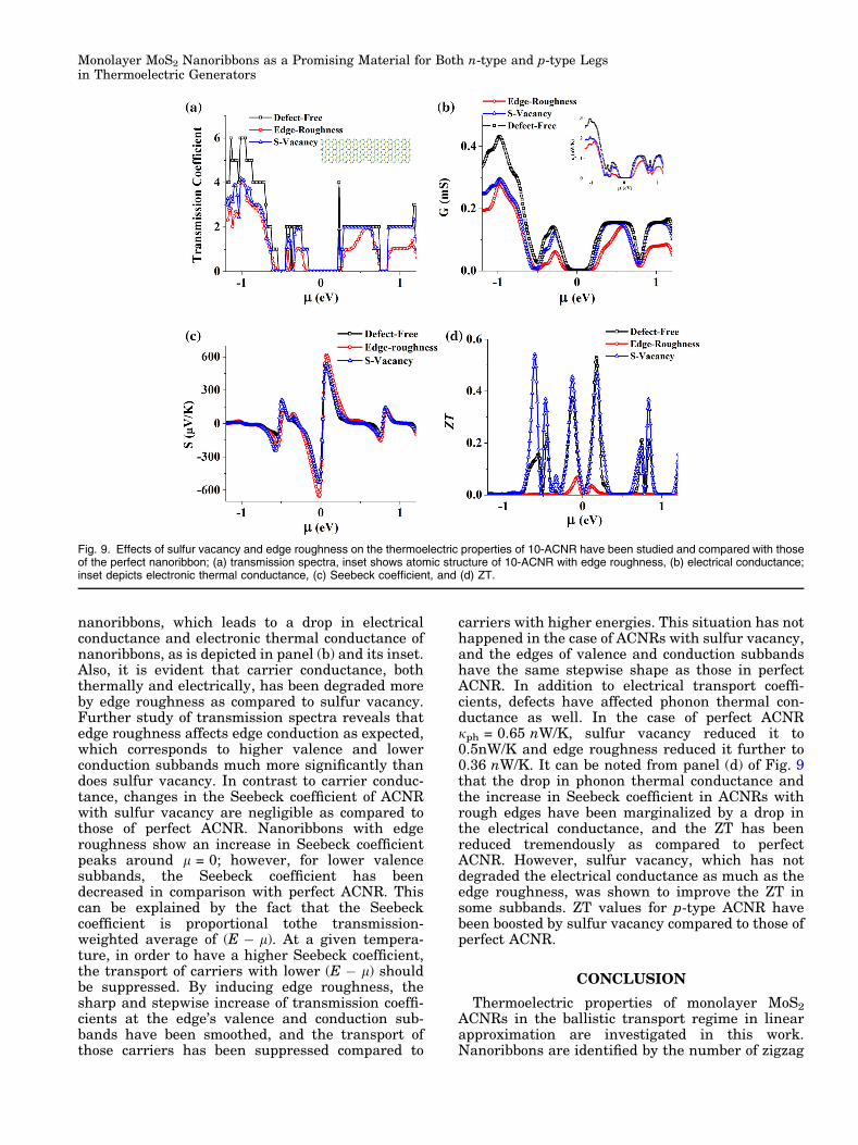
nanoribbons, which leads to a drop in electricalconductance and electronic thermal conductance ofnanoribbons, as is depicted in panel (b) and its inset.Also, it is evident that carrier conductance, boththermally and electrically, has been degraded moreby edge roughness as compared to sulfur vacancy.Further study of transmission spectra reveals thatedge roughness affects edge conduction as expected,which corresponds to higher valence and lowerconduction subbands much more significantly thandoes sulfur vacancy. In contrast to carrier conduc-tance, changes in the Seebeck coefficient of ACNRwith sulfur vacancy are negligible as compared tothose of perfect ACNR. Nanoribbons with edgeroughness show an increase in Seebeck coefficientpeaks around l = 0; however, for lower valencesubbands, the Seebeck coefficient has beendecreased in comparison with perfect ACNR. Thiscan be explained by the fact that the Seebeckcoefficient is proportional tothe transmission-weighted average of (E � l). At a given tempera-ture, in order to have a higher Seebeck coefficient,the transport of carriers with lower (E � l) shouldbe suppressed. By inducing edge roughness, thesharp and stepwise increase of transmission coeffi-cients at the edge’s valence and conduction sub-bands have been smoothed, and the transport ofthose carriers has been suppressed compared to
carriers with higher energies. This situation has nothappened in the case of ACNRs with sulfur vacancy,and the edges of valence and conduction subbandshave the same stepwise shape as those in perfectACNR. In addition to electrical transport coeffi-cients, defects have affected phonon thermal con-ductance as well. In the case of perfect ACNRjph = 0.65 nW/K, sulfur vacancy reduced it to0.5nW/K and edge roughness reduced it further to0.36 nW/K. It can be noted from panel (d) of Fig. 9that the drop in phonon thermal conductance andthe increase in Seebeck coefficient in ACNRs withrough edges have been marginalized by a drop inthe electrical conductance, and the ZT has beenreduced tremendously as compared to perfectACNR. However, sulfur vacancy, which has notdegraded the electrical conductance as much as theedge roughness, was shown to improve the ZT insome subbands. ZT values for p-type ACNR havebeen boosted by sulfur vacancy compared to those ofperfect ACNR.
CONCLUSION
Thermoelectric properties of monolayer MoS2
ACNRs in the ballistic transport regime in linearapproximation are investigated in this work.Nanoribbons are identified by the number of zigzag
Fig. 9. Effects of sulfur vacancy and edge roughness on the thermoelectric properties of 10-ACNR have been studied and compared with thoseof the perfect nanoribbon; (a) transmission spectra, inset shows atomic structure of 10-ACNR with edge roughness, (b) electrical conductance;inset depicts electronic thermal conductance, (c) Seebeck coefficient, and (d) ZT.
Monolayer MoS2 Nanoribbons as a Promising Material for Both n-type and p-type Legsin Thermoelectric Generators

chains across them and denoted as N-ACNR. Theeffect of the size of nanoribbons on their thermo-electric behavior by considering N = 3–10 has beenstudied. Transmission spectra of ACNRs are com-prised of edge subbands for both electrons andholes. This leads to the existence of three gaps intransmission spectra. It has been shown that theband gap at l = 0 increases as ACNRs widens,except for those with N = 3, p � 1, in which p is aninteger that has higher band gaps than neighboringones. As the width of ACNRs increases, the Seebeckcoefficient and ZT around l = 0 both increase.Phonon thermal conductance decreases as ACNRsnarrow due to an increased impact of phonon edgescattering. As a result, the maximum ZT values thatcan be achieved by narrow ACNRs are higher thanthe wider ones. The effect of sulfur vacancy andedge roughness on thermoelectric properties is alsoinvestigated. It is found that, although edge rough-ness will reduce phonon thermal conductance, thedegradation in electrical conductance leads to atremendous drop in ZT. In contrast to edge rough-ness, a sulfur vacancy reduces the phonon thermalconductance without degrading electrical conduc-tance as much as edge roughness, leading to anincreased ZT value at some energies. It has beenshown that ZT values as high as ZT = 4 in 3-ACNRfor n-type material and ZT = 3 in 4-ACNR for p-typematerial at T = 500 K can be achieved. The possi-bility of gaining high ZT values for both n-type andp-type material makes monolayer MoS2 ACNRs apromising candidate in future thermoelectricgenerators.
REFERENCES
1. K.S. Novoselov, A.K. Geim, S.V. Morozov, D. Jiang, Y.Zhang, S.V. Dubonos, I.V. Grigorieva, and A.A. Firsov,Science 306, 5696 (2004).
2. Y. Zhang, Y.-W. Tan, H.L. Stormer, and P. Kim, Nature438, 7065 (2005).
3. A.C. Ferrari, J.C. Meyer, V. Scardaci, C. Casiraghi, M.Lazzeri, F. Mauri, S. Piscanec, D. Jiang, K.S. Novoselov, S.Roth, and A.K. Geim, Phys. Rev. Lett. 97, 18 (2006).
4. K.S. Novoselov, A.K. Geim, S.V. Morozov, D. Jiang, M.I.Katsnelson, I.V. Grigorieva, S.V. Dubonos, and A.A. Firsov,Nature 438, 7065 (2005).
5. R.F. Frindt, J. Appl. Phys. 37, 4 (1966).6. A. Schumacher, L. Scandella, N. Kruse, and R. Prins, Surf.
Sci. 289, 1 (1993).7. Y. Li, Z. Zhou, S. Zhang, and Z. Chen, J. Am. Chem. Soc.
130, 49 (2008).8. L. Kou, C. Tang, Y. Zhang, T. Heine, C. Chen, and T.
Frauenheim, J. Phys. Chem. Lett. 3, 20 (2012).9. C. Ataca, H. Sahin, E. Akturk, and S. Ciraci, J. Phys.
Chem. C 115, 10 (2011).10. K.K. Kam and B.A. Parkinson, J. Phys. Chem. 86, 4 (1982).11. K.F. Mak, C. Lee, J. Hone, J. Shan, and T.F. Heinz, Phys.
Rev. Lett. 105, 13 (2010).12. B. Radisavljevic, A. Radenovic, J. Brivio, V. Giacometti,
and A. Kis, Nat. Nanotechnol. 6, 3 (2011).13. E. Gourmelon, J.C. Bernede, J. Pouzet, and S. Marsillac, J.
Appl. Phys. 87, 3 (2000).14. B. Radisavljevic, M.B. Whitwick, and A. Kis, ACS Nano 5,
12 (2011).15. S. Yu, K. Eshun, H. Zhu, and Q. Li, Sci. Rep. (2015). doi:
10.1038/srep12854.
16. A. Kuc, N. Zibouche, and T. Heine, Phys. Rev. B 83, 24(2011).
17. Y. Pei, A. LaLonde, S. Iwanaga, and G.J. Snyder, EnergyEnviron. Sci. 4, 6 (2011).
18. K. Biswas, J. He, I.D. Blum, C.-I. Wu, T.P. Hogan, D.N.Seidman, V.P. Dravid, and M.G. Kanatzidis, Nature 489,7416 (2012).
19. L.D. Hicks and M.S. Dresselhaus, Phys. Rev. B 47, 19(1993).
20. L.D. Hicks and M.S. Dresselhaus, Phys. Rev. B 47, 24(1993).
21. M.S. Dresselhaus, G. Chen, M.Y. Tang, R.G. Yang, H. Lee,D.Z. Wang, Z.F. Ren, J.-P. Fleurial, and P. Gogna, Adv.Mater. 19, 8 (2007).
22. D.M. Rowe, V.S. Shukla, and N. Savvides, Nature 290, 765(1981).
23. A.I. Hochbaum, R. Chen, R.D. Delgado, W. Liang, E.C.Garnett, M. Najarian, A. Majumdar, and P. Yang, Nature451, 7175 (2008).
24. X. Shi, L. Chen, J. Yang, and G.P. Meisner, Appl. Phys.Lett. 84, 2301 (2004).
25. R. Mansfield and S.A. Salam, Proc. Phys. Soc. Sect. B 66, 5(1953).
26. M. Buscema, M. Barkelid, V. Zwiller, H.S. van der Zant,G.A. Steele, and A. Castellanos-Gomez, Nano Lett. 13, 2(2013).
27. X. Liu, G. Zhang, Q.-X. Pei, and Y.-W. Zhang, Appl. Phys.Lett. 103, 13 (2013).
28. J.-W. Jiang, H.S. Park, and T. Rabczuk, J. Appl. Phys. 114,6 (2013).
29. G. Huai-Hong, Y. Teng, T. Peng, and Z. Zhi-Dong, Chin.Phys. B 23, 1 (2014).
30. M.K. Agarwal and L.T. Talele, Solid State Commun. 59, 8(1986).
31. S.G. Thakurta and A.K. Dutta, J. Phys. Chem. Solids 44, 5(1983).
32. H. Guo, T. Yang, P. Tao, Y. Wang, and Z. Zhang, J. Appl.Phys. 113, 1 (2013).
33. J.-W. Jiang, X. Zhuang, and T. Rabczuk, Sci. Rep. 3, 2209(2013).
34. A. Arab and Q. Li, Sci. Rep. 5, 1306 (2015).35. D. Wickramaratne, F. Zahid, and R.K. Lake, J. Chem.
Phys. 140, 12 (2014).36. Q. Li, E.C. Walter, W.E. Van der Veer, B.J. Murray, J.T.
Newberg, E.W. Bohannan, J.A. Switzer, J.C. Hemminger,and R.M. Penner, J. Phys. Chem. B 109, 8 (2005).
37. Q. Li, J.T. Newberg, E.C. Walter, J.C. Hemminger, andR.M. Penner, Nano Lett. 4, 2 (2004).
38. X. Liu, T. Xu, X. Wu, Z. Zhang, J. Yu, H. Qiu, J.-H. Hong,C.-H. Jin, J.-X. Li, X.-R. Wang, L.-T. Sun, and W. Guo, Nat.Commun. 4, 3121 (2013).
39. Y.-C. Lin, W. Zhang, J.-K. Huang, K.-K. Liu, Y.-H. Lee, C.-T. Liang, C.-W. Chu, and L.-J. Li, Nanoscale 4, 20 (2012).
40. I. Song, C. Park, M. Hong, J. Baik, H.-J. Shin, and H.C.Choi, Angew. Chem. Int. Ed. 53, 5 (2014).
41. S. Najmaei, Z. Liu, W. Zhou, X. Zou, G. Shi, S. Lei, B.I.Yakobson, J.-C. Idrobo, P.M. Ajayan, and J. Lou, Nat.Mater. 12, 8 (2013).
42. A.M. van der Zande, P.Y. Huang, D.A. Chenet, T.C.Berkelbach, Y. You, G.-H. Lee, T.F. Heinz, D.R. Reichman,D.A. Muller, and J.C. Hone, Nat. Mater. 12, 6 (2013).
43. K. Kang, S. Xie, L. Huang, Y. Han, P.Y. Huang, K.F. Mak,C.-J. Kim, D. Muller, and J. Park, Nature 520, 7549 (2015).
44. D.D. Fan, H.J. Liu, L. Cheng, P.H. Jiang, J. Shi, and X.F.Tang, Appl. Phys. Lett. 105, 13 (2014).
45. M. Brandbyge, J.-L. Mozos, P. Ordejon, J. Taylor, and K.Stokbro, Phys. Rev. B 65, 16 (2002).
46. M. Buttiker, Y. Imry, R. Landauer, and S. Pinhas, Phys.Rev. B 31, 10 (1985).
47. H.J. Monkhorst and J.D. Pack, Phys. Rev. B 13, 12 (1976).48. S. Datta, Quantum Transport: Atom to Transistor (Cam-
bridge: Cambridge University Press, 2005), pp. 285–312.49. F.H. Stillinger and T.A. Weber, Phys. Rev. B 31, 8
(1985).
Arab, Davydov, Papaconstantopoulos, and Li

50. Y. Cai, G. Zhang, and Y.-W. Zhang, J. Am. Chem. Soc. 136,17 (2014).
51. H. Pan and Y.-W. Zhang, J. Mater. Chem. 22, 15 (2012).52. A.R. Botello-Mendez, F. Lopez-Urias, M. Terrones, and H.
Terrones, Nanotechnology 20, 32 (2009).53. H. Zheng, Z.F. Wang, T. Luo, Q.W. Shi, and J. Chen, Phys.
Rev. B 75, 16 (2007).54. L. Pan, H.J. Liu, X.J. Tan, H.Y. Lv, J. Shi, X.F. Tang, and
G. Zheng, Phys. Chem. Chem. Phys. 14, 39 (2012).55. Y. Ouyang and J. Guo, Appl. Phys. Lett. 94, 26 (2009).
56. J.-W. Jiang, J.-S. Wang, and B. Li, J. Appl. Phys. 109, 1(2011).
57. Z. Guo, D. Zhang, and X.-G. Gong, Appl. Phys. Lett. 95, 16(2009).
58. H. Fang, M. Tosun, G. Seol, T.C. Chang, K. Takei, J. Guo,and A. Javey, Nano Lett. 13, 5 (2013).
59. D. Kiriya, M. Tosun, P. Zhao, J.S. Kang, and A. Javey, J.Am. Chem. Soc. 136, 22 (2014).
60. H. Fang, S. Chuang, T.C. Chang, K. Takei, T. Takahashi,and A. Javey, Nano Lett. 12, 7 (2012).
Monolayer MoS2 Nanoribbons as a Promising Material for Both n-type and p-type Legsin Thermoelectric Generators