modular multi-signal tracking pulse descriptor word (pdw
TRANSCRIPT

Wright State University Wright State University
CORE Scholar CORE Scholar
Browse all Theses and Dissertations Theses and Dissertations
2016
Modular Multi-Signal Tracking Pulse Descriptor Word (PDW) Modular Multi-Signal Tracking Pulse Descriptor Word (PDW)
Generator with Field Programmable Gate Array (FPGA) Generator with Field Programmable Gate Array (FPGA)
Implementation Implementation
Justin Darrell Pelan Wright State University
Follow this and additional works at: https://corescholar.libraries.wright.edu/etd_all
Part of the Electrical and Computer Engineering Commons
Repository Citation Repository Citation Pelan, Justin Darrell, "Modular Multi-Signal Tracking Pulse Descriptor Word (PDW) Generator with Field Programmable Gate Array (FPGA) Implementation" (2016). Browse all Theses and Dissertations. 1561. https://corescholar.libraries.wright.edu/etd_all/1561
This Thesis is brought to you for free and open access by the Theses and Dissertations at CORE Scholar. It has been accepted for inclusion in Browse all Theses and Dissertations by an authorized administrator of CORE Scholar. For more information, please contact [email protected].

MODULAR MULTI-SIGNAL TRACKING PULSE DESCRIPTOR WORD (PDW)
GENERATOR WITH FIELD PROGRAMMABLE GATE ARRAY (FPGA)
IMPLEMENTATION
A thesis submitted in partial fulfillment
of the requirements for the degree of
Master of Science in Engineering
By
Justin Darrell Pelan
B.S. Wright State University, 2013
2016
Wright State University

WRIGHT STATE UNIVERSITY
GRADUATE SCHOOL
August 17, 2016
I HEREBY RECOMMEND THAT THE THESIS PREPARED UNDER MY
SUPERVISION BY Justin Darrell Pelan ENTITLED Modular Multi-Signal Tracking
Pulse Descriptor Word (PDW) Generator With Field Programmable Gate Array (FPGA)
Implementation BE ACCEPTED IN PARTIAL FULFILLMENT OF THE
REQUIREMENTS FOR THE DEGREE OF Master of Science in Engineering.
Committee on
Final Examination
_________________________________
J.M. Emmert Ph.D.
_________________________________
Saiyu Ren Ph.D.
_________________________________
Raymond E. Siferd Ph.D.
______________________________
Robert E. W. Fyffe, Ph.D.
Vice President for Research and
Dean of the Graduate School
J.M. Emmert, Ph.D.
Thesis Director
Brian Rigling, Ph.D.
Chair, Department of
Electrical Engineering

iii
ABSTRACT
Pelan, Justin. M.S. Egr., Department of Electrical Engineering, Wright State University,
2016, Modular Multi-Signal Tracking Pulse Descriptor Word (PDW) Generator With
Field Programmable Gate Array (FPGA) Implementation.
As signal spectra become dense, the task of tracking and identifying radars
becomes increasingly cumbersome. The variety of radars in modern theaters of war
compound the task due to simultaneous operation. Real-time processing of large data sets
prove difficult for sequential systems, and the parallelism of Field Programmable Gate
Arrays (FPGAs) becomes an attractive option. To mitigate the increasing complexity of
this task, this design proposes an FPGA architecture to produce pulse descriptor words
(PDW) for up to eight independent radio frequency signals that can be used in near-real-
time processing. Focusing on digital hardware techniques and modular design allow for
flexibility to target specific signal aspects such as carrier frequency (F), signal amplitude
(A), time of arrival (TOA), and pulse width (PW).

iv
Table of Contents
I. INTRODUCTION ....................................................................................................... 1
II. BACKGROUND ..................................................................................................... 3
III. PDW Generator ...................................................................................................... 13
IV. Results .................................................................................................................... 30
V. Conclusions ............................................................................................................ 49
VI. REFERENCES ...................................................................................................... 50

v
LIST OF FIGURES
Figure 1: Simple Radar with Target Diagram..................................................................... 3
Figure 2: Simple Radar Component Diagram .................................................................... 4
Figure 3: Time vs. Amplitude of Radar Pulses ................................................................... 8
Figure 4: Theoretical Signal List, Time I............................................................................ 9
Figure 5: Theoretical Signal List, Time I + 1 ................................................................... 11
Figure 6: High Level Block Diagram ............................................................................... 13
Figure 7: Stage 1 Block Diagram...................................................................................... 14
Figure 8: Digital Number Bins with Example Sine Wave ................................................ 16
Figure 9: Stage 2 Monobit FFT Diagram ......................................................................... 17
Figure 10: Stage 3 Block Diagram.................................................................................... 19
Figure 11: Stage 4 Block Diagram.................................................................................... 20
Figure 12: Sorting Registers Block Diagram .................................................................... 21
Figure 13: Cascading Sorting Registers ............................................................................ 22
Figure 14: Tracking Logic Block ...................................................................................... 23
Figure 15: Comparator Bank – Current to Old 0 .............................................................. 24
Figure 16: Internal View of Comparator Bank ................................................................. 25
Figure 17: Flow Chart of Tracking Block......................................................................... 27
Figure 18: Single Stage 4 Tracking Block ........................................................................ 28
Figure 19: Single 2.5 MHz Signal in Temporal Domain .................................................. 32
Figure 20: Power Spectral Density of Single Signal ........................................................ 33

vi
Figure 21: Multiple Signals in Temporal Domain ............................................................ 34
Figure 22: Power Spectral Density of 4 Equally Spaced Signals ..................................... 34
Figure 23: Power Spectral Density of 256 Point Matlab FFT .......................................... 35
Figure 24: Stage 3 Magnitude Output for Single Signal................................................... 36
Figure 25: Stage 3 Magnitude Output for 2 Signals ......................................................... 37
Figure 26: Stage 3 Magnitude Output for 3 Signals ......................................................... 37
Figure 27: Stage 3 Magnitude Output for 4 Signals ......................................................... 38
Figure 28: Power Spectral Density of 256 Point Matlab FFT, 4 Signals ......................... 38
Figure 29: Stage 3 Output for 2 Signals with Bin Labels ................................................. 39
Figure 30: Stage 4 Sorting Register Outputs .................................................................... 40
Figure 31: OR Gate Output from Sorting Registers ......................................................... 41
Figure 32: Stage 4 Tracking Block Independent Test Case .............................................. 42
Figure 33: PDW Generator Output Waveform Clk 17 ..................................................... 43
Figure 34: PDW Generator Output Waveform Clk 18 ..................................................... 44
Figure 35: PDW Generator Output Waveform Clk 19 ..................................................... 44
Figure 36: Direct Stimulation of Frequency Bins – CLK Period 35 ................................ 46
Figure 37: Direct Stimulation of Frequency Bins – CLK Period 36 ................................ 47
Figure 38: Direct Stimulation of Frequency Bins – VHDL iSim Waveform ................... 48

vii
LIST OF TABLES
Table 1: Historical / NATO / EW Bands Streetly, Martin. "Introduction." Jane's Radar
and Electronic Warfare Systems, 2002-2003. Coulsdon, Surrey, UK: Jane's Information
Group, 2002. Page 5. Print. ................................................................................................. 5
Table 2: Additional Radar Range Equation Terms ............................................................. 6
Table 3: Signal Amplitude to Digital Number Conversion Conditions ............................ 15
Table 4: Possible OR Gate Output Combinations ............................................................ 26
Table 5: PDW Output – CLK 17 – Decimal Form ........................................................... 45
Table 6: PDW Output – CLK 18 – Decimal Form ........................................................... 45
Table 7: PDW Output – CLK 19 – Decimal Form ........................................................... 45

viii
ACKNOWLEDGEMENTS
I would like to thank my wonderful family for their unconditional love, support,
and encouragement from start to finish of this thesis. My mother Evelyn, father Darrell,
sister Lauren, and girlfriend Renee give me the strength to go on as they always help
remind me that family is most valuable in life. I would be truly lost without you.
I must extend a special thank you to Dr. J.M. Emmert, for his invaluable advice
and support during the completion of this Thesis. Our technical discussions have brought
great insight to this work, and your mentorship throughout both my undergraduate and
graduate work has helped shaped me into the engineer I am today.
I would like to thank the outstanding people at the Wright State University
Electrical Engineering department that inspire, support, and challenge me to do my best.
It is an honor working with you and I look forward to our future interactions.
Finally, I extend a thank you to my committee for their time and effort in the
review and defense of my thesis.

1
I. INTRODUCTION
Modern warfare was forever changed since the invention of tactical RAdio Detection
and Ranging (Radar) systems in the 1930’s. It is an invaluable tool that extended the
sensing capabilities of modern systems for a variety of military and civilian applications.
Alongside the invention of radar the field of Electronic Warfare (EW) was born, which
contains the three major categories of Electronic Support Measures (ESM), Electronic
Attack (EA), and Electronic Protection (EP) [1]. ESM is dedicated to the task of
information gathering about electromagnetic signals in the environment, which includes
(but is not limited to) detection, interception, identification, and recording. EA primarily
deals with employing countermeasures that exploit the weakness of threat systems, and
EP are the methods by which systems are guarded against the damaging or performance
degrading effects of EA.
This work focuses on the intercepted signals from threat radars in an environment
which mostly falls into the ESM realm as other systems rely on information provided to
apply an appropriate EA or EP response. Wiley refers to the interception of signals and
interpretation of system functionality as electronic intelligence (ELINT) [2]. He stresses
that the ability to ascertain potential threats in an environment while outside of
operational range of hostile force is a situational advantage. A specific example being
from World War II (WWII) where British RAF used L-band search radars to locate
German U-boats while surfacing. The addition of L-band receivers on the U-boats alerted
them to the threatening radars detecting them, thus providing enough time to dive out of
harm’s way [2].

2
A modern popular method to gain an approximation of present signals in an
environment is to generate Pulse Descriptor Words (PDW) from the measurements made
by an intercepting receiver or possibly a radar warning receiver (RWR) [3]. The PDWs
are generally multiple measurements made on received pulses that are then grouped
together in a single data package. The packages can contain measurements such as carrier
frequency (F), signal amplitude (A), time of arrival (TOA), and pulse width (PW).
Subsequent systems are then able to use the valuable information to perform post-
analysis. While this can be useful for mission planning, some situations require a real-
time or near-real-time response to threats during a mission. For example if a missile
system is using a lock on radar to track and engage a target, the response time of the
warning system, and the pilot must be extremely quick in order to deploy lifesaving chaff
countermeasures. The widespread use of digital electronics in technology has also rose to
answer this call as automated countermeasure systems report a system latency in the tens
to hundreds of milliseconds [3].
Multiple digital hardware platforms exist to implement warning receivers such as
FPGAs (Field Programmable Gate Arrays), ASICS (Application Specific Integrated
Circuits), CPUs (Central Processing Units), and GPUs (Graphical Processing Units).
Each has distinct advantages and disadvantages depending on the required application in
electronic warfare. FPGAs have great flexibility in the prototyping arena as different
physical hardware blocks can be removed or inserted by changing code alone. The rest of
the list has a static set of multiplies, adders, and logic units in which it must use to
execute the task in often sequential order (save GPUs). Keeping this in mind with a near-
real-time processing requirement, FPGAs will be the focus of this work.

3
II. BACKGROUND
2.1 Radar – Radio Detection and Ranging
Radio Detection and Ranging (Radar) is the application of transmitting radio frequency
(RF) electromagnetic waves into a scene, and then deducing information about the scene
based off measurements made from the reflections. Targets, clutter, and other physical
matter reflect the transmitted energy in all directions when they come in contact with one
another [4]. Figure 1 below shows a simplified diagram of a radar emitting an RF wave
and then receiving a portion of the energy that reflected off the target. Earlier Radar
systems were limited to target detection and target range estimation, but modern systems
have evolved to be far more sophisticated devices capable of detection, range estimation,
speed estimation, radar countermeasures, scene imaging, tracking, and other capabilities
[5].
Figure 1: Simple Radar with Target Diagram

4
The first generation of tactical radars existed in the 1930’s in major countries such as
Germany, USA, and Great Britain [6]. Each country created an almost equally capable
system of detection and ranging with components such as a transmitter, circulator,
antenna, low noise amplifier, mixer, local oscillator, and a detector. Figure 2 below
illustrates a generalized setup for the analog front end of an early style radar. Modern
digital radars will add the additional blocks of an analog-to-digital converter (ADC) and a
signal processor in place of the detector. Depending on the operational frequency of the
radar, more or less components will be added to meet the required applications.
Figure 2: Simple Radar Component Diagram
The frequency bands at which radars operated during WWII and the 1969 North Atlantic
Treaty Organization (NATO) frequency bands are listed in Table 1 [7]. Although the
NATO bands are sometimes referred to as EW bands due to their specific application in
the field of electronic warfare. The table does not cover the entire electromagnetic

5
spectrum at which radars work, but the majority of modern functional systems still adhere
to these band designations.
Table 1: Historical / NATO / EW Bands Streetly, Martin. "Introduction." Jane's Radar
and Electronic Warfare Systems, 2002-2003. Coulsdon, Surrey, UK: Jane's Information
Group, 2002. Page 5. Print.
Historical Radar Bands NATO / EW Bands
Band Designation Frequency (GHz) Band Designation Frequency (GHz)
VHF1 0.03 – 0.3 A 0.03 – 0.25
UHF2 0.3 – 1 B 0.25 – 0.5
L 1 – 2 C 0.5 – 1
S 2 – 4 D 1 – 2
C 4 – 8 E 2 – 3
X 8 – 12 F 3 – 4
Ku 12 – 18 G 4 – 6
K 18 – 27 H 6 – 8
Ka 27 – 40 I 8 – 10
MM3 40 – 100 J 10 – 20
1. Very High Frequency
2. Ultra High Frequency
3. Millimetric
K 20 – 40
L 40 – 60
M 60 – 100
With the aforementioned setup and frequency spectrum it is assumed that the
electromagnetic waves generated by the radar system will travel through space at the
speed of light c approximated to 3 x 10⁸ m/sec, travel a range in kilometers R to a target,
and have a time difference of ΔT from transmit to receive. The waves must travel from
the transmitter of the radar, reflect off of a target in scene, and then return to the receiver
of the radar for processing. This induces a factor of 2 to be used in the denominator for

6
equation (1) as the definition of ΔT is usually in terms of total time traveled, rather than
time traveled to the target [4].
𝑅 =cΔT
2 (1)
Typically radars are operated by emitting a series of pulsed waves, or by emitting a
constant wave (CW). Assuming a pulsed operation radar system, equation 1 can be
modified to include the following parameters:
Table 2: Additional Radar Range Equation Terms
PR Power Received (W)
PT Power Transmitted (W)
GT Transmitter Gain
GR Receiver Gain
λ Wavelength (m)
σ Target radar cross section
(square meters)
LT Transmitter loss
LR Receiver Loss
𝑃𝑅 =PT𝐺𝑇𝐺𝑅𝜆2𝜎
(4π)3𝑅4𝐿𝑇𝐿𝑅 (2)
Equation 2 is now the classic radar range equation that describes the power received after
a pulse has traveled to the target and then to the receiver [4]. It should be noted that the
range (R) is inversely proportional to the receiver power (PR) due to signal spreading
when traveling to and from the target [2]. If an intercept receiver is actively listening for

7
radar signals in an environment, a similar equation can be assumed for the power
received at the intercept receiver.
𝑃𝐸 =PT𝐺𝑇𝐸𝐺𝐸𝜆2
(4π)2𝑅𝐸2𝐿𝑇𝐿𝐸
(3)
The additional terms of ELINT receiver signal power (PE), transmitter gain in ELINT
receiver direction (GTE), ELINT receiver gain (GE), ELINT receiver loss (LE), and
range from transmitter to ELINT receiver (RE) now represent the power signal model to
approximate received pulses from threat emitters to an intercepting receiver [2].
2.2 Radar Pulse Measurements and Pulse Descriptor Words
Measurements of radar pulses are combined into a single data packet known as a Pulse
Descriptor Word (PDW). PDWs usually include basic radar parameters such as Pulse
Width (PW), Radar Carrier Frequency (RF), Pulse Repetition Interval (PRI), Pulse
Repetition Frequency (PRF), Time of Arrival (TOA), Difference of Time of Arrival
(DTOA), Angle of Arrival (AOA), Amplitude (A), Signal to Noise Ratio (SNR), and
many other possible parameters. PDWs can vary system to system dependent on the
application as some measurements are more useful in identifying potential targets or
foreign emitters.

8
Figure 3: Time vs. Amplitude of Radar Pulses
Figure 3 illustrates an pulsed radar waveform in the time domain with a PW of 0.5uS,
PRI of 2uS, TOAs of 2uS and 4uS, RF of 10Mhz, and an amplitude of 1 arbitrary units.

9
2.3 Problem Statement
Tracking signals simultaneously in near-real-time proves to be a difficult task as the
complexity of keeping an ordered list according to signal magnitude or signal bins
increases as the total number of signals rises. Post-processing systems have the luxury of
time as no immediate threats are enforcing a time constraint on the system. To meet the
stringent requirement, a parallelized signal tracking block will be implemented on a Virtex
6 FPGA development board, tested with eight simultaneous signal inputs.
The main architecture used to implement this block would be a set of registers and a
large counter to keep track of signal beginning and ending times. Figure 4 below shows
the basic register bank which orders the signals according to bin number from smallest to
largest for simplicity.
Figure 4: Theoretical Signal List, Time I
K denotes the last signal number, as well as the maximum allowable number of signals
to be stored in the register. At any instantaneous time I there are anywhere from 0 to K

10
signals being tracked. This allows the register to start, continue, or stop tracking signals at
time I + 1.
2.3.3 Start New Signal Tracking
Since we are interested in radar applications, the tracking of a signal should start when
the signal magnitude exceeds that of a designated threshold. This then requires the
resister block to insert the signal into the current stored data set according to its spectral
bin number. The signal’s start time is also recorded in order to show it’s relation to other
signals within the register and to determine its length when the signal’s magnitude once
again falls below the desired threshold.
Not only will the new signal have to be sorted to be correctly placed, the current data
will have to be shifted in order to make room for the new “slot” in the register bank.
Figure 5 shows the sorting and insertion process into the register bank with a signal new
signal. The possibility of multiple new signals will exceed the threshold at the same time
instant which causes a dilemma in the sorting and shifting process. One solution would
be to sort and then shift the data accordingly one at a time, unfortunately this defeats the
purpose of drastically increasing processing time.

11
Figure 5: Theoretical Signal List, Time I + 1
2.3.1 Continual Signal Tracking
When the signal magnitude remains above the threshold at a time of I + n, the
register content should not change and only the counter increases as time goes on. This
successfully records the detected signals over any period of time, and can still provide
the instantaneous signal values at any time I.
2.3.2 Stop Signal Tracking
Once the signal has fallen below the threshold, the register bank will then perform
the opposite action of removing the signal from the register bank along with recording
the ending time of the signal. This will paint a clear picture of the signal length.
For example, if the new Signal 4 started at time I + 1 in Figure 5 and was inserted
into the proper location according to its bin number of 6, and then ended at a time of I
+ 2, the signal length would be a time unit of 1. Figure 5 illustrates the process of

12
removing data from the register bank and then shifting the old data in order to take its
place.

13
III. PDW Generator
3.1 Block Diagram
The proposed pulse descriptor word generator is divided into five stages to
separate each of the sequential data handling operations. Each of the five stages use a
modular design so that different implementations of the block can be easily substituted in
for rapid testing and prototyping. Figure 6 below shows seven high level blocks within
the five stages providing an outline for the core design.
Figure 6: High Level Block Diagram

14
The RF front end and post processing hardware are not thoroughly discussed in
this design, but both blocks are represented in Figure 6 to provide context on where this
processing chain is envisioned to fit in a system. The serial input shift register block
shown in Figure 7 is the first step in passing the temporal amplitude values from the
analog RF front end to the digital PDW generator.
3.2 Stage 1
Figure 7: Stage 1 Block Diagram
The symbols NI, NB, and NP respectively stand for the input data bit width,
number of input bits per sample, and the number of points for the Fast Fourier Transform
block. Defining each symbol as constant in the main package of the source code allows
for design flexibility. Since each stage must be compatible with the previous one’s inputs,
the symbols are used extensively throughout the design to determine hardware bit sizes.
Signals, inputs, and outputs will be appropriately changed if a symbol’s value is altered.

15
This saves the hardware designer a time consuming process of reading through hundreds
of lines of VHDL and chasing down debug errors.
As an example we assign NI = 16, NB = 2, and NP = 16. The corresponding Stage
1 input is calculated to be a 16 element array, with 2 bit vectors in each element for a
total of 32 bits while the output is an array of 256 elements and 2 bit vectors. Inspecting
Figure 7 further shows that there will be NI or 16 D-Flip Flops with each output being
sequentially connected to the input of the next D-Flip Flop and to the final output array.
By passing data through each of the D-Flip Flops it will move from the first 16 elements
in the 256 output array to the last within NI clock ticks.
The reasoning behind the NB = 2 section is partly due to the design choice of
using a Monobit Fast Fourier Transform (FFT) architecture for improved speed
performance. This sacrifices accuracy in the FFT calculation, but is justified by the near-
real time requirement coupled with an 8 signal tracking goal. With only two bits for
amplitude measurements, the conditionals displayed in Table 3 are applied to data that
has been scaled between 1 and -1.
Table 3: Signal Amplitude to Digital Number Conversion Conditions
If Amplitude >= 0.5 Input = “11”
If Amplitude >= 0 Input = “10”
If Amplitude >= -0.5 Input = “01”
Else Input = “00”
The 16 element input array is now filled with a sequence of temporal samples from the
analog RF front end which will propagate through the 256 element output. Figure 8
below is a visual representation of the conditional bins for a single cycle sine wave.

16
Figure 8: Digital Number Bins with Example Sine Wave
Notice in Figure 8 how a signal amplitude value above or equal the black line will
produce a “11” within the input array, a value between the black and blue lines will
produce a “10”, a value between the blue and red lines will produce a “01”, and finally a
value below the red line will produce a “00”.

17
3.3 Stage 2
Figure 9: Stage 2 Monobit FFT Diagram
Stage 2 consists of a Monobit Fast Fourier Transform (FFT) to convert the signal
amplitudes from the temporal domain into frequency domain. It uses symbols NP, number
of points for the FFT, and NM , the number of magnitude bits that will be generated from
Stage 3. This specific FFT architecture outputs I (real) and Q (imaginary) arrays with
NP/2 elements that each contain a vector of (NM -1)/2 bits. Continuing with the example
outlined in Stage 1 we will assume that NP = 256 and set NM = 15, this causes each I and
Q vector to be 7 bits wide. The (NM -1)/2 calculation is based off the fact that the Stage 3
magnitude estimation has an addition operation in it. Whenever 2 numbers of bit width M
are added, the resulting bit width of the sum must be M + M + 1 to account for any
overflow. For example, if M = 3 bits the largest number that can be represented is “111”

18
and if we add two numbers that are 3 bits wide, the resulting sum will need 4 bits to
handle the overflow and accurately represent the resulting sum, “111” + “111” = “1011”.
It is also worth mentioning that the clock input to Stage 1 is labeled as “CLK”
while the one in Stage 2 is labeled as “CLK_F”. This is due to the fact that Stage 1 and
Stage 2 operate on different time scales. Stage 2 will wait until there have been
NP/(NB*NI) clock ticks so that the shift register has acquired a full set of samples.
Keeping the previous values of NP = 256, NB = 2, and NI = 16 the second clock signal,
CLK_F, should occur only once per 8 ticks of CLK. The rest of the design will also work
off of the CLK_F signal as new frequency domain values will only be available at each
operation of the FFT.

19
3.4 Stage 3
Figure 10: Stage 3 Block Diagram
The previous Stage 2 formats the I and Q outputs into a NP element array that contain
(NM -1)/2 bit wide vectors. This means that there are NP/2 elements for the I values, and
NP/2 elements for the Q values. When combined into magnitudes they create NP/2
frequency bins by using the following approximations:
𝑆𝑖𝑔𝑛𝑎𝑙 𝑀𝑎𝑔𝑛𝑖𝑡𝑢𝑑𝑒 = 𝐼2 + 𝑄2 (number)
This differs from the conventional calculation of:
𝑆𝑖𝑔𝑛𝑎𝑙 𝑀𝑎𝑔𝑛𝑖𝑡𝑢𝑑𝑒 = √𝐼2 + 𝑄2 (number)
Square root calculations are temporally and spatially expensive to perform in digital
hardware. Time and space savings are significant enough to compensate for the minimal
loss of accuracy in the magnitude calculation.

20
3.5 Stage 4
Figure 11: Stage 4 Block Diagram
Stage 4 is the final module primarily tasked with handling signal tracking and pulse
descriptor word (PDW) generation. The previous output from Stage 3, size NP/2 * NM, is
the number of frequency bins NP/2 and the magnitude of each bin having bit width NM.
This information is particularly useful to distinguish independent signal characteristics
that may be otherwise impossible to discern from temporal amplitude values. This design
monitors the signal start, signal stop, signal continuation, signal magnitude, and signal
frequency bin address in each of the NSIG available channels. Each of the blocks in Stage
4 will be discussed in depth starting with the Sorting Registers block and ending with the
PDW Generator.

21
Figure 12: Sorting Registers Block Diagram
Sorting Registers are the first block that are inside of Stage 4 tasked to generate a sorted
list of largest magnitude values at any time T. While finding the single largest magnitude
of an array is not difficult, finding NSIG largest signals in decreasing order is a much
harder challenge to accomplish.
A cascading architecture containing Largest Magnitude, Zero Out, and D-Flip Flop
(DFF) blocks are used in order to generate the sorted signal list. The Largest Magnitude
blocks take an array input of NP/2 elements to output the largest magnitude and its
address in the array. An updated array of NP/2 elements with the current largest
magnitude removed is provided to the next Largest Magnitude block by the Zero Out
block. It uses a the address information from the previous Largest Magnitude block to
replace the current largest magnitude with ‘0’s. The next largest magnitude block then
determines the largest magnitude in the array and repeats the architecture for NSIG times.

22
Each stage of this operation is guarded by a set of DFF to ensure the largest magnitude
measurements temporarily match and largest magnitudes are not mixed up clock tick to
clock tick. Figure 13 blow shows a higher level block diagram without the Zero Out
blocks to better illustrate the addtional DFF it takes by increasing NSIG.
Figure 13: Cascading Sorting Registers
If each of the NSIG largest magnitudes cannot be found in parallel, then this
architecture proposes to find each largest magnitude sequentially with extra hardware to
keep the temporal book keeping straight. This does cause the design to require NSIG clock
ticks delay at startup, but data can be accurately sampled at each clock tick after the
delay. This increases the required space of the design as well due to the fact that each
DFF has to keep track of one magnitude signal of NM bits and one address signal of NA
bits. Now that a sorted list of the largest NSIG magnitudes has been generated, the act of
tracking each signal magnitude can be performed.

23
The Tracking Logic block must first determine if a signal is present long enough to be
tracked. A magnitude and address that is present for a single clock tick should be ignored
as it may well be noise or other anomaly. To ensure that the current signals are indeed
worth tracking, the Tracking Logic block starts with 2 DFF that take all NSIG channels as
inputs. The important internal signals called “Current”, “Old 0”, and “Old 1” are
generated to determine if a signal is present for at least 2 clock ticks.
Figure 14: Tracking Logic Block
It is important to note in Figure 14 above that the DFF not holding magnitudes, but
frequency bin addresses instead. This design assumes that a signal will fluctuate in
magnitude quite often, but will not change its frequency bin address. There are current
systems where emitters will emit RF signals that change frequently quite often as chirps,
and frequency hoppers. Tracking these complex signals will require additional hardware
logic to target specific waveforms.
24
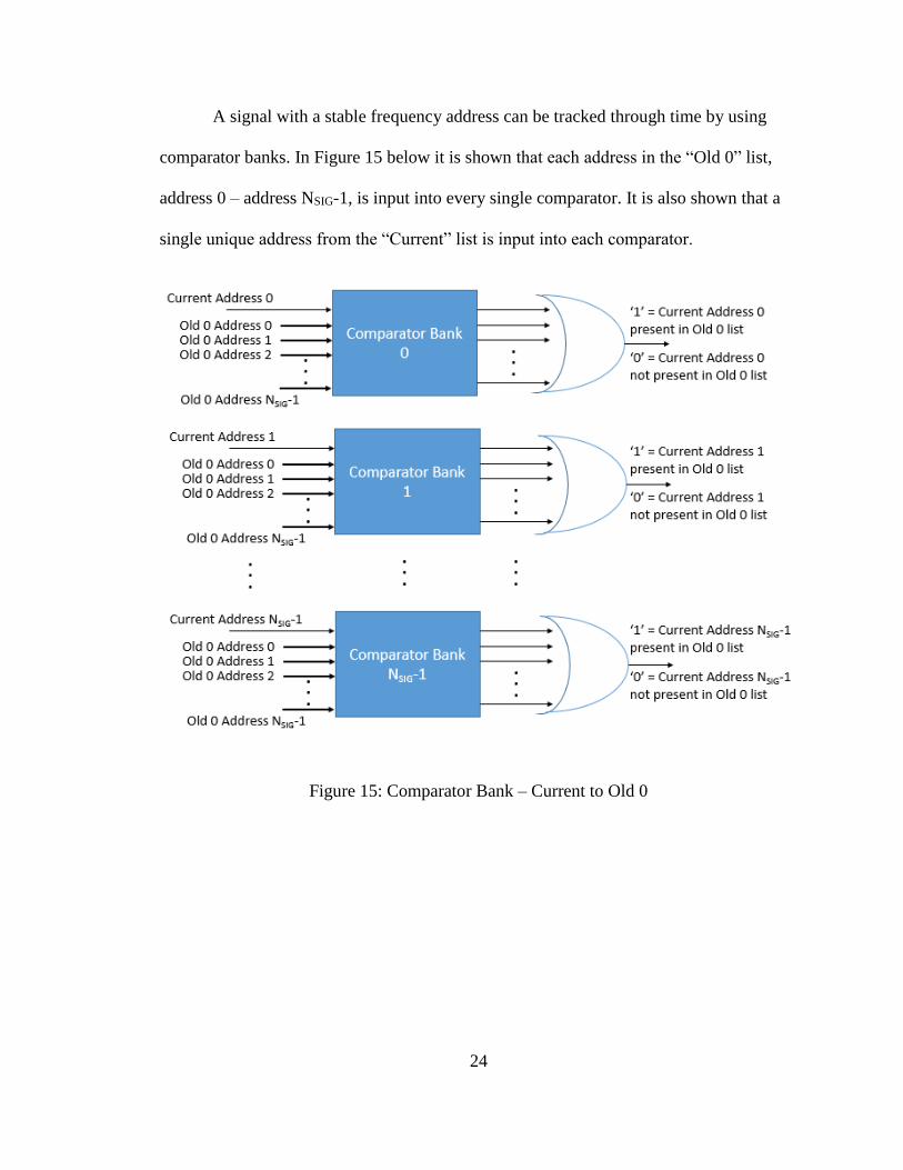
A signal with a stable frequency address can be tracked through time by using
comparator banks. In Figure 15 below it is shown that each address in the “Old 0” list,
address 0 – address NSIG-1, is input into every single comparator. It is also shown that a
single unique address from the “Current” list is input into each comparator.
Figure 15: Comparator Bank – Current to Old 0

25
Figure 16: Internal View of Comparator Bank
The Comparator Bank will then output a vector of bit width NSIG-1, and in each element
of the vector will be a single bit of ‘0’ or ‘1’. If “Current Address 0” is equal to the
respective “Old 0 Address X” (X = 0,1,…NSIG-1), then a ‘1’ will be output by the
comparator, and a ‘0’ will be output otherwise. Figure 16 above shows all of the NSIG-1
comparator outputs are connected to an OR gate to determine if the “Current” address is
found within the “Old 0” address list. By repeating this architecture with the “Old 1”
address list, the “Current” address list is compared to both the “Old 0” and “Old 1”
address lists in parallel. Each OR gate output from the “Old 0” comparator bank is
compared to its counterpart from the “Old 1” comparator bank OR gates. A summary of
the possible temporal signal states is shown below in Table 4.

26
Table 4: Possible OR Gate Output Combinations
OR Gate Output of Old 0 OR Gate Output of Old 1 Relation To Signal
‘0’ ‘0’ The address in this channel
is brand new and has not
been seen for the last 2
clock periods.
‘0’ ‘1’ The address in this channel
has been seen 2 clock
periods ago, but not in the
last clock period.
‘1’ ‘0’ The address in this channel
has been present for 1 clock
period.
‘1’ ‘1’ The address in this channel
has been seen for 2
consecutive clock periods.
The current information available at this point in the design is as follows: a largest
to smallest array of size NSIG with NM sized vectors (sorted signal magnitude list), a
corresponding array of size NSIG with NA sized vectors (contains the frequency bin
address for each of the magnitudes in the sorted list), and two vectors of size NSIG that
determine if a signal has been present for 0, 1, or 2 clock periods (Old 0 and Old 1). By
using this information the Tracking Logic block will determine the Time of Arrival
(TOA) and Pulse Width (PW) in each of the NSIG channels.
Figure 17 below shows a flow chart of the algorithm used to determine the time of
arrival and pulse width of signals. The tracking logic starts with concentrating on a single
address of only one channel. It will continually receive address values from the channel
until the OR gate outputs from “Old 0” and “Old 1” indicate that the address has been
present for 2 clock periods. At this point the tracking block will hold this address value
and ignore all others until it is no longer present in the signal list.

27
Figure 17: Flow Chart of Tracking Block
After the tracking block starts to track or hold an address, it will set an internal variable
for the time of arrival when it started tracking the time. This time value comes from a
simple external counter that continually counts and resets when it reaches maximum
value. The tracking block is now in the “Is address present at next clock period” block in
Figure 17 as it will check address channels 0 to NSIG-1 every clock period to ensure that
the address it started tracking is still present. It will continually update the pulse width
(PW) for every clock period that the address is present. When the tracked address finally

28
disappears from the sorted address list, the tracking block will output the pulse width
(PW), and time of arrival (TOA). The tracking block will also clear all internal variables
and ready itself to receive another address for tracking.
Figure 18: Single Stage 4 Tracking Block
The figure above illustrates how each tracking block requires a “Current Address to
be tracked” which can be a vector of size NA from any single channels. This address will
be compared to all other current addresses which will also all be NA sized vectors. The
“Old 0” and “Old 1” OR Outputs are from the previously mentioned comparator banks to
determine if the “Current Address to be track” has been present for at least 2 clock
periods. Finally, the “Clock Time” input will be used to determine TOA and eventually
PW when the signal ends. It is a simple calculation of Time of Arrival (TOA) – Ending
Time.

29
Stage 4 now has access to the magnitude, frequency bin address, pulse width, and
time of arrival for each of the 0 to NSIG-1 channels. The final step is to combine each of
the measurements into a single large vector for each channel. This vector will be of size
LT + LT + NM + NA, where LT is the bit width of the time vectors, NM is the bit width of
the signal magnitude vector, and NA is the bit width of the frequency bin address. The
values are simply directly wired into the final channel vector, as in bits NA-1 down to 0
will be reserved for the frequency bin address value, bits NA + NM-1 down to NA will be
reserved for the signal magnitude address and so forth.

30
IV. Results
The Pulse Descriptor Word Generator is implemented using VHSIC Hardware
Description Language (VHDL) with a specific target platform of a Xilinx Virtex 6 Field
Programmable Gate Array (FPGA) development board. Simulated results will first be
discussed with a short follow on discussion covering a synthesized design of the same
test cases.
4.1 Signal Characteristics
To find the limitations of signal frequencies the Xilinx Virtex 6 Development
Board technical details are taken into consideration. A 200 MHz clock is available which
will be connected to the Stage 1 Serial Register and will serve as the sampling frequency
for the Stage 2 Monobit FFT. Calculating the period as T = 1 / F or T = 1 / 200 MHz
yields a 5 ns sampling period. Adding a 25% of additional time now gives an assumed
worst case propagation delay of 6.25 ns. Normally, with a 200 MHz sampling frequency
fS it is assumed from Nyquist sampling [9] that the highest detectable frequency will be fS
/ 2 or in this case 200 MHz /2 = 100 MHz. With the added delay for the Worst Case
Propagation Delay (WPD) being 6.25 ns, the sampling frequency now becomes 160 MHz
and the highest detectable frequency will now be 80 MHz.
4.2 Stage 1 Serial Register Parameter Settings
We will use the parameter values that were given in section III PDW Generator
when going through example test cases of this design. Starting with Stage1 Serial
Register, the bit width per sample NB = 2, and the number of samples or the input data bit

31
width NI = 16. It will also adhere to the bit division to convert the signal amplitude values
into digital numbers from Table III above.
4.3 Stage 2 Monobit FFT Parameter Settings
For this stage NP = 256 so the FFT will have 256 points or samples, and will
output 128 real (I) frequency bins, and 128 imaginary (Q) frequency bins. Each of the
bins are (NM-1) / 2 bit width in size where NM is selected to be 15. Keeping in mind that
the sampling frequency fS above was calculated to be 160 MHz and that there are 256
points within the FFT, each bin should be have a frequency width of fS / FFT points or
160 MHz / 256 = 625 KHz.
4.4 Stage 3 Magnitude Approximation
With the previous Stage 2 Monobit FFT providing 128 real and imaginary bins,
NM is still equal to 15 for this case. That allows each of the bins to be 7 bits wide, which
will then be multiplied together and then added to each other. The output of a hardware
multiplier that has two input values of bit width M will require the output to be of size
2*M. Since each of the I and Q addresses will be multiplied by itself before being added
the bit width of the output becomes 14 and then 15 after the addition.
4.5 Stage 4 Tracking Logic
Stage 4 is the largest of the stages. It takes NSIG channels, 8 channels in this test
case, which are made up of a magnitude value and an address value. The magnitude value
is dependent on the parameter NM which is set to 15, and the address of the frequency
bin is dependent on NA which is 7.

32
4.6 Test Cases
This initial test case demonstrates the data flow through the PDW generator to
validate the operation of each stage. The input data was generated in Matlab by using the
same sampling frequency fS of 160MHz with a worst case propagation delay of 6.25 ns.
We will try to spread the 8 signals out evenly between the 128 frequency bins, but taking
into account the first and last 4 frequency bins are ignored leaves 120 bins to work with.
That means that if the first signal is centered on bin 4, it should be 4 * 0.625 or 2.5 MHz.
Figure 19: Single 2.5 MHz Signal in Temporal Domain

33
Figure 20: Power Spectral Density of Single Signal
Figure 20 above shows the power spectral density of the first signal that will be generated
and input into the PDW generator. To equally space out an additional 7 signals, the 120
available frequency bins are divided by 8, so there should be 15 bins between signals. If
the first signal is centered in bin 4, then the second should be in bin 19, the third in bin
34, and so on. This yields frequencies of 2.5 MHz, 11.875 MHz, 21.25 MHz, and 30.725
MHz for the first four signals which can be seen below in Figure 21.

34
Figure 21: Multiple Signals in Temporal Domain
Figure 22: Power Spectral Density of 4 Equally Spaced Signals

35
The power spectral density figures were generated in Matlab using the complex conjugate
of the FFT and a large amount of FFT points to have high resolution in estimating the
frequency bins. This allows for a high accuracy in estimating the correct frequency for
the input. When going through the PDW generator, the Monobit FFT is restricted to 256
points and will decrease the accuracy of the frequency estimation.
Figure 23: Power Spectral Density of 256 Point Matlab FFT
The power spectral density graphs are now estimated using a 256 point FFT in Matlab to
simulate what the output should look like for the output of the Stage 3 magnitude
estimation. The magnitude values will not match due to the missing square root part of
the calculation, but it should mirror the frequency bins well.

36
Figure 24: Stage 3 Magnitude Output for Single Signal
The single 2.5 MHz cases match well for the 256 point Matlab FFT and the Stage 3
Magnitude approximation VHDL simulation. The peaks are both found within the 4th
frequency bin, but the Matlab estimation is less nosiy. This is due to the fact that the
Monobit FFT uses only the 4 different digital number estimations of “00”, ”01”, “10”,
and “11” when looking at the signal amplitudes. The Matlab FTT calculates each of the
amplitude signal values as doubles and has greatly increased accuracy when performing
calculations. This limitation also causes problems when the number of signals are linearly
increased.

37
Figure 25: Stage 3 Magnitude Output for 2 Signals
Figure 26: Stage 3 Magnitude Output for 3 Signals
38
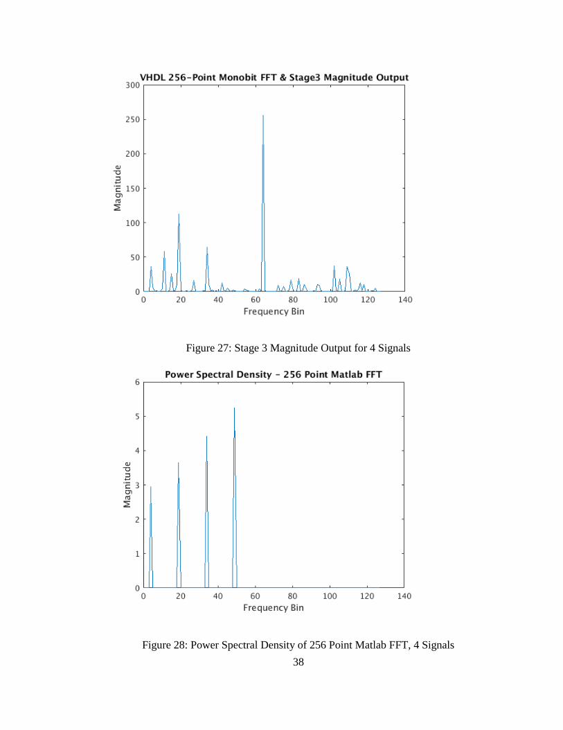
Figure 27: Stage 3 Magnitude Output for 4 Signals
Figure 28: Power Spectral Density of 256 Point Matlab FFT, 4 Signals

39
As seen above the output from Stage 3 Magnitude Approximation is incorrect
after the 3rd signal is added to the input values. The magnitudes are further degraded after
a 4th signal is added, and Figures 27 and 28 show the large difference in what the Matlab
estimate is to what Stage 3 provided during simulation. For this initial case, we will look
at the 2 signal input case as it provides multiple distinct peaks to test Stage 4.
Figure 29: Stage 3 Output for 2 Signals with Bin Labels
By looking at the outputs from Stage 3 above, the largest to smallest bins should be 4, 19,
34, 49, 15 or 65, 11, and 83 with respective magnitudes of 325, 260, 140, 80, 65, 50, 45.
These results can be compared to the waveform shown in the following figures.

40
Figure 30: Stage 4 Sorting Register Outputs
As seen above the sorting registers do not immediately output a sorted signal list of
magnitudes and addresses. It takes approximately NSIG clock periods to produce the
correct output when there are NSIG signals present. The signal list labeled “opl” represents
the signal magnitudes in each of the 0 to 7 channels with channel 0 being the largest.
Each channel must also contain a frequency bin address which is labeled “opr” and also
follows the same convention so that each of the elements in “opl” match the elements in
“opr”. At the 700 ns mark the outputs of the sorting registers match to the expected
outputs of the largest being the signal in address 4 with a magnitude of 81, and the
smallest in address 83 with a magnitude of 10. Looking at Figure 29 shows that the
magnitudes should be approximately 4 times larger than the results reported by the
sorting registers. This is due to an internal clipping operation where the 2 least significant
bits are removed from each of the magnitudes to save on area and speed. A factor of 4 is
introduced into the magnitudes by this operation to save time and area.

41
The next waveform shows the outputs of the OR gates to determine if a signal has
been present for 0, 1, or 2 clock periods.
Figure 31: OR Gate Output from Sorting Registers
It is seen that in Figure 31 the “compor0” and “compor1” signals are only 1 bit in width
and have 8 channels as well. The “compor0” should be a ‘1’ for any given channel if it
has been present for at least 1 clock period. Notice how channel 7 has 2 peaks that are
fighting for the spot on the list every other clock period. This causes the channel 7 of
“compor0” to never activate due to the switching nature of the 2 signals. However
compor1 is a ‘1’ for channel 7 due to the fact that each of the signals was seen 2 clock
periods ago, and it is now present in the channel once again. The majority of the other
channels show that both “compor0” and “compor1” are ‘1’ for each of them. They have a
static place in the list for this test case, which is easy for the Stage 4 Tracking Block.

42
Figure 32: Stage 4 Tracking Block Independent Test Case
Before using the Stage 4 Tracking Block in this test case, an independent test
bench was written to accurately control the inputs. Figure 32 shows the output from a
single tracking block, which is only the TOA and PW. The “taa” signal variable stands
for tracking address where the block is latched on that address until it disappears from the
signal list. Notice at approximately 100 ns that the address value 9 disappears from the
list and is instead replaced by 7, and the other address values in the list are shifted. The
block realizes this change and holds the PW value until it latched onto the new address it
is supposed to latch onto. After the tracking block finds that address 7 has been present
for 2 clock periods, it then restarts the PW and TOA variables and continues to track the
new signal. The tracking block will now be used in the previous test case.

43
Figure 33: PDW Generator Output Waveform Clk 17
Figures 33 – 35 are in fact all the same screenshot of the PDW Generator output, but each
has the cursor marked at a different clock period. The “Output” signal is the final product
of the PDW Generator and has the TOA, PW, Magnitude, and Frequency Bin Address
combined into a single large number. The outputs have been changed from binary into
unsigned int to save space while displaying. The binary should be 32 bits + 32 bits + 15
bits + 7 bits long. This corresponds to how TOA, PW, Magnitude, and Address are
combined into a single logic vector from most significant bit to least significant bit.

44
Figure 34: PDW Generator Output Waveform Clk 18
Figure 35: PDW Generator Output Waveform Clk 19

45
Table 5: PDW Output – CLK 17 – Decimal Form
Table 6: PDW Output – CLK 18 – Decimal Form
Table 7: PDW Output – CLK 19 – Decimal Form
Notice how the TOA takes one clock period to update before it becomes the correct value
and the pulse width will continually update so long as the signal is still present. Each of

46
the signals in this case are continuously present in the same bin and there is little change
in the list. The next test case will use direct stimulation of the frequency bins to generate
a more difficult test case.
Figure 36: Direct Stimulation of Frequency Bins – CLK Period 35
In Figure 36 above the first stages are bypassed in order to generate 8 signals that can
be freely manipulated in magnitude and frequency bin. This allows the Stage 4 PDW
tracker to be more precisely tested with cases where the signals prove to be more difficult
to track. The 8 signals will continue to be present in the first half of this simulation, and
the second half will only contain 4 signals. Frequency bins and magnitudes of 4 signals
will be changed to simulate the fading and arrival of signals in the list.

47
Figure 37: Direct Stimulation of Frequency Bins – CLK Period 36
The resulting signal list is represented by Figure 37 where 3 signals have remained and 5
have been removed or changed in the list. The PDW generator should continue to track
the 3 signals that remained and start tracking the new signals that appeared.
Signals with frequency bin address in 13, 33, and 67 persist through the second
half of the test case as seen in Figure 38. Their Pulse Widths (PW) are still in the 30’s
after the signal switch, while the other signals revert back to a 0 pulse width case. The
Time of Arrivals (TOA) are also consistent throughout the test case which indicates the
tracking block is still working as intended.

48
Figure 38: Direct Stimulation of Frequency Bins – VHDL iSim Waveform
The PDW Generator was then synthesized to a Virtex 6 FPGA development board
for hardware implementation and testing. The worst case propagation delay for the
sampling frequency CLK in the synthesize report was 7.61ns while the larger CLK_F that
drives the majority of the logic reported a 18.21ns WPD. This may change when the
design is mapped into the FPGA, but there was a limiting amount of input / output pins
on the device to properly implement the design. The PDW generator is currently being
redesigned to bypass the pin problem. The synthesis report also determined that 6% of
the total slice registers, 54% of the total slice LUTS, and 17% of fully used LUT-FF pairs
were used in order to synthesize the current design.

49
V. Conclusions
The Pulse Word Descriptor Generator seeks to solve the task of tracking multiple
signals in near-real time. It uses 4 separate stages in order to first perform the FFT of the
incoming signal amplitudes, estimate the magnitude of the signals using sum of squares,
and then finally sorting and tracking the signals. The design was developed as a modular
testbed for future work to easily replace stages with different implementations of the
same block to quickly prototype different architectures. Specifically the Monobit FFT
falls short when more than 2 signals are present at a given time. A more robust FFT block
that may take more time should be considered if tracking multiple signals accurately and
in parallel is the main focus. Additional accuracy was also sacrificed in the interest of
speed by the square root removal in the magnitude calculation. This does introduce an
accuracy error in regards to the signal magnitudes, as well as trimming 2 bits off of the
signal vectors. Although these do cause slight problems in the ordering of signals, it is
not enough to drastically change the ordering and tracking of the truly largest to smallest
signals. The PDW Generator can be changed in a variety of ways for the designer to
quickly prototype RF signal processing algorithms in an FPGA.
50
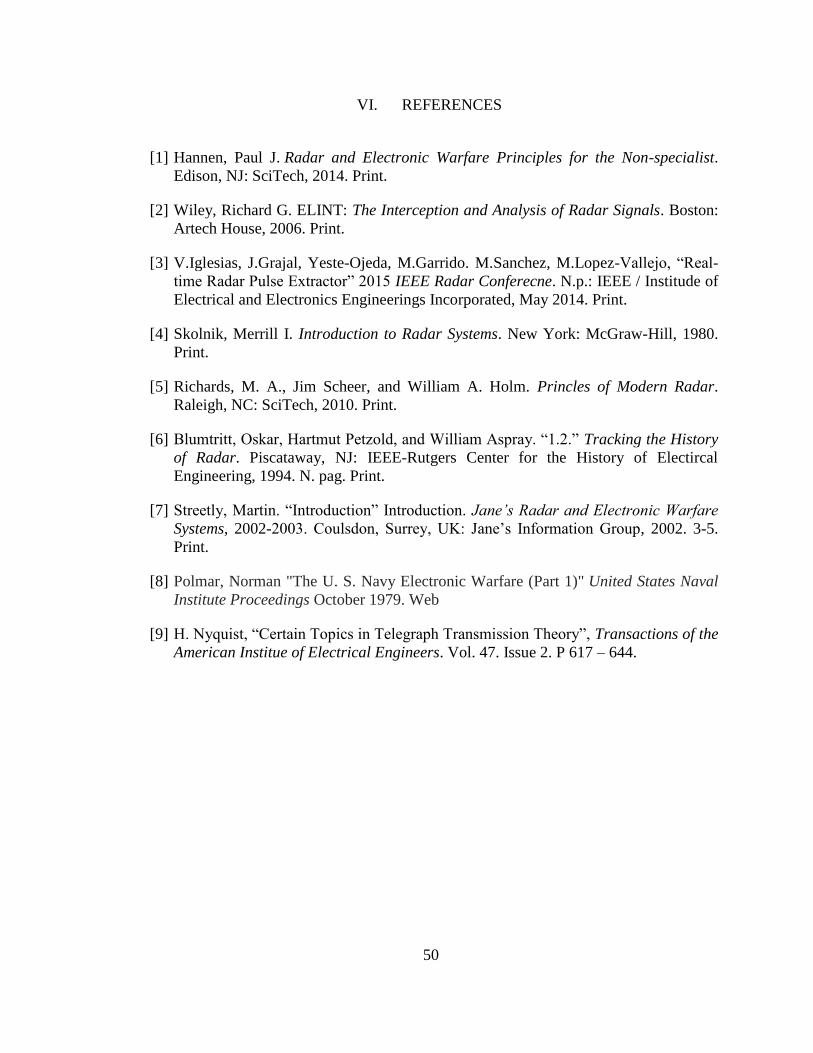
VI. REFERENCES
[1] Hannen, Paul J. Radar and Electronic Warfare Principles for the Non-specialist.
Edison, NJ: SciTech, 2014. Print.
[2] Wiley, Richard G. ELINT: The Interception and Analysis of Radar Signals. Boston:
Artech House, 2006. Print.
[3] V.Iglesias, J.Grajal, Yeste-Ojeda, M.Garrido. M.Sanchez, M.Lopez-Vallejo, “Real-
time Radar Pulse Extractor” 2015 IEEE Radar Conferecne. N.p.: IEEE / Institude of
Electrical and Electronics Engineerings Incorporated, May 2014. Print.
[4] Skolnik, Merrill I. Introduction to Radar Systems. New York: McGraw-Hill, 1980.
Print.
[5] Richards, M. A., Jim Scheer, and William A. Holm. Princles of Modern Radar.
Raleigh, NC: SciTech, 2010. Print.
[6] Blumtritt, Oskar, Hartmut Petzold, and William Aspray. “1.2.” Tracking the History
of Radar. Piscataway, NJ: IEEE-Rutgers Center for the History of Electircal
Engineering, 1994. N. pag. Print.
[7] Streetly, Martin. “Introduction” Introduction. Jane’s Radar and Electronic Warfare
Systems, 2002-2003. Coulsdon, Surrey, UK: Jane’s Information Group, 2002. 3-5.
Print.
[8] Polmar, Norman "The U. S. Navy Electronic Warfare (Part 1)" United States Naval
Institute Proceedings October 1979. Web
[9] H. Nyquist, “Certain Topics in Telegraph Transmission Theory”, Transactions of the
American Institue of Electrical Engineers. Vol. 47. Issue 2. P 617 – 644.