modeling and simulation of 1700 v 8 a genesic
TRANSCRIPT
University of Arkansas, Fayetteville University of Arkansas, Fayetteville
ScholarWorks@UARK ScholarWorks@UARK
Graduate Theses and Dissertations
8-2016
Modeling and Simulation of 1700 V 8 A GeneSiC Superjunction Modeling and Simulation of 1700 V 8 A GeneSiC Superjunction
Transistor Transistor
Staci E. Brooks University of Arkansas, Fayetteville
Follow this and additional works at: https://scholarworks.uark.edu/etd
Part of the Electromagnetics and Photonics Commons, and the Electronic Devices and
Semiconductor Manufacturing Commons
Citation Citation Brooks, S. E. (2016). Modeling and Simulation of 1700 V 8 A GeneSiC Superjunction Transistor. Graduate Theses and Dissertations Retrieved from https://scholarworks.uark.edu/etd/1740
This Thesis is brought to you for free and open access by ScholarWorks@UARK. It has been accepted for inclusion in Graduate Theses and Dissertations by an authorized administrator of ScholarWorks@UARK. For more information, please contact [email protected].

Modeling and Simulation of 1700 V 8 A GeneSiC Superjunction Transistor
A thesis submitted in partial fulfillment
of the requirements for the degree of Master of Science in Microelectronics-Photonics
by
Staci Erin Brooks
Henderson State University
Bachelor of Science in Physics, 2011
August, 2016
University of Arkansas
This thesis is approved for recommendation to the Graduate Council.
Dr. H. Alan Mantooth
Thesis Director Dr. Gregory Salamo Tom Vrotsos
Committee Member Committee Member
Dr. Rick Wise
Ex-Officio Member

The following signatories attest that all software used in this thesis was legally licensed for use
by Staci E. Brooks for research purposes and publication.
__________________________________ __________________________________
Ms. Staci E. Brooks, Student Dr. H. Alan Mantooth, Thesis Director
This thesis was submitted to http://www.turnitin.com for plagiarism review by the TurnItIn
company’s software. The signatories have examined the report on this thesis that was returned by
TurnItIn and attest that, in their opinion, the items highlighted by the software are incidental to
common usage and are not plagiarized material.
__________________________________ __________________________________
Dr. Rick Wise, Program Director Dr. H. Alan Mantooth, Thesis Director
ABSTRACT
The first-ever 1.7kV 8A SiC physics-based compact SPICE model is developed for
behavior prediction, modeling and simulation of the GeneSiC “Super” Junction Transistor. The
model implements Gummel-Poon based equations and adds a quasi-saturation collector series
resistance representation from a 1.2 kV, 6 A SiC bipolar junction transistor model developed in
Hangzhou, China. The model has been validated with the GA08JT17-247 device data
representing both static and dynamic characteristics from GeneSiC. Parameter extraction was
performed in IC-CAP and results include plots showing output characteristics, capacitance
versus voltage (C-V), and switching characteristics for 25 °C, 125 °C, and 175 °C temperatures.

ACKNOWLEDGEMENTS
This work was made possible under the leadership and advisement of Dr. H. Alan
Mantooth and Ranbir Singh at the GeneSiC Semiconductor Company. Ranbir and GeneSiC were
extremely generous in providing devices for testing within our device modeling lab.
Acknowledgement is also due to Tom Vrotsos for his continuous involvement and guidance for
the duration of this project.
Lastly, a Special Thanks to Michael Leonard, Shamim Ahmed, Sonia Perez, and Dr. Matt
Francis for their roles of support.

DEDICATION
This thesis is dedicated to the people that believe I can do anything, thanks Emanuel III
and Darla Brooks (whom I affectionately call Mom and Dad) for your unwavering faith in me
and my abilities; also, to all Friends and Family that have supported this journey
This work is especially dedicated to my one true love and biggest encourager, Travis Adams.
Thank you for being my strength through this process and letting me cry, but not letting me quit.
I am eternally grateful for the life we get to share together.

TABLE OF CONTENTS
CHAPTER 1: INTRODUCTION ........................................................................................................ 1 1.1 Semiconductor Device Modeling ........................................................................................... 1
1.1.1 Purpose and Importance of Device Modeling ................................................................... 1
1.1.2 Model Simulators and HDLs ............................................................................................. 2
1.2 GeneSiC “Super” Junction Transistor ................................................................................. 3
1.2.1 Semiconductor Superjunction Device Theory ................................................................... 4
1.2.2 GeneSiC SJT Device Applications .................................................................................... 5
1.3 Thesis Structure ...................................................................................................................... 5
CHAPTER 2: SIC AS A DEVICE MATERIAL ............................................................................. 6 2.1 SiC in Power Electronics ........................................................................................................ 6
2.2 Material and Electrical Properties ........................................................................................ 6
2.2.1 SiC Structure and Polytypes .............................................................................................. 6
2.2.2 Wide Bandgap .................................................................................................................... 7
2.2.3 Critical Electric Field ......................................................................................................... 9
2.2.4 Thermal Conductivity ........................................................................................................ 9
CHAPTER 3: BJT PRINCIPLE OVERVIEW .............................................................................. 10 3.1 Basic Operation of BJTs ....................................................................................................... 10
3.2 Power BJT ............................................................................................................................. 11
3.2.1 Power BJT Structure and Operation ................................................................................ 11
3.2.2 Operating Principles ........................................................................................................ 13
3.2.3 Output Characteristics ...................................................................................................... 16
3.2.4 Switching Characteristics ................................................................................................ 17
CHAPTER 4: SJT MODEL ............................................................................................................... 18 4.1 Current State of SiC BJT/SJT Models................................................................................ 18
4.1.1 SiC BJT Models ............................................................................................................... 18

4.1.2 SiC SJT Models ............................................................................................................... 20
4.2 Model Description ................................................................................................................. 20
4.2.1 Static Equations ............................................................................................................... 21
4.2.2 Quasi-Saturation Model ................................................................................................... 24
4.2.3 Dynamic Equations .......................................................................................................... 25
4.3 Temperature Scaling ............................................................................................................ 27
CHAPTER 5: MODEL SIMULATION AND VERIFICATION .............................................. 30 Evaluating Model Performance ................................................................................................. 30
5.1 Parameter Extraction and Simulation Analysis................................................................. 30
5.1.1 Parameter Extraction ........................................................................................................ 30
5.1.2 Simulation Results and Verification ................................................................................ 36
5.1.3 Temperature Scaled Results ............................................................................................. 44
5.2.2 C-V and Switching Characteristics .................................................................................. 46
CHAPTER 6: SUMMARY AND CONCLUSIONS ...................................................................... 51 Future Work ................................................................................................................................ 51
REFERENCES ...................................................................................................................................... 53
APPENDIX A: DESCRIPTION OF RESEARCH FOR POPULAR PUBLICATION........ 56
APPENDIX B: EXECUTIVE SUMMARY OF NEWLY CREATED INTELLECTUAL
PROPERTY............................................................................................................................................ 57
APPENDIX C: POTENTIAL PATENT AND COMMERCIALIZATION ASPECTS OF
LISTED INTELLECTUAL PROPERTY ITEMS ........................................................................ 58
APPENDIX D: BROADER IMPACT OF RESEARCH ............................................................. 59 D.1 Applicability of Research Methods to Other Problems .................................................... 59
D.2 Impact of Research Results on U.S. and Global Society .................................................. 59
D.3 Impact of Research Results on Environment .................................................................... 59
APPENDIX E: MICROSOFT PROJECT FOR MS MICROEP DEGREE ........................... 60

APPENDIX F: IDENTIFICATION OF ALL SOFTWARE USED IN RESEARCH AND
THESIS GENERATION ..................................................................................................................... 61

LIST OF FIGURES
Fig. 2.1: Basic crystal structural unit of SiC. .................................................................................. 6
Fig. 2.2: Common SiC crystal polytype stacks. .............................................................................. 7
Fig. 2.3: Intrinsic carrier concentration comparison of Si and 4H-SiC over temperature. ............. 8
Fig. 3.1: The four BJT modes of operation. .................................................................................. 10
Fig. 3.2: Basic power BJT structure. 𝐽1 represents the base-emitter junction and 𝐽2
represents the base-collector junction. .......................................................................................... 12
Fig. 3.3: Electron flow in NPN power bipolar transistor. ............................................................. 13
Fig. 3.4: Internal currents of the bipolar transistor. ...................................................................... 14
Fig. 3.5: Stored charge distribution in BJT normal active region. ................................................ 15
Fig. 3.6: Output characteristics of power transistor. ..................................................................... 17
Fig. 4.1: Symbol and Equivalent Circuit for use of SJT model. ................................................... 21
Fig. 5.1: Simulation test bench circuits used for (a) output characteristics (b) base-emitter
C-V (c) base-collector C-V and (d) switching simulations. ......................................................... 37
Fig. 5.2: SJT output characteristics at room temperature (25 ˚C). ................................................ 38
Fig. 5.3: (a) Base-emitter and (b) base-collector C-V characteristics. .......................................... 40
Fig. 5.4: SJT turn-on switching (a) current characteristics and (b) voltage characteristics at
room temperature. ......................................................................................................................... 42
Fig. 5.5: SJT turn-off switching (a) current characteristics and (b) voltage characteristics at
room temperature. ......................................................................................................................... 43
Fig. 5.6: Output Characteristics for (a) 125 °C and (b) 175 °C. ................................................... 45
Fig. 5.7: Turn-on current characteristics temperature comparison for 125 °C and 175 °C. ......... 47
Fig. 5.8: Turn-on current characteristics simulated at 175 °C. ..................................................... 47
Fig. 5.9: Turn-on voltage characteristics temperature comparison of 125 °C and 175 °C. .......... 48
Fig. 5.10: Turn-on voltage characteristics simulated at 175 °C. ................................................... 48

Fig. 5.11: Turn-off current characteristics temperature comparisons for 125 °C and 175 °C. ..... 49
Fig. 5.12: Turn-off current characteristics simulated at 175 °C. .................................................. 49
Fig. 5.13: Turn-off voltage characteristics comparison for 125 °C and 175 °C. .......................... 50
Fig. 5.14: Turn-off voltage characteristics simulated at 175 °C. .................................................. 50
LIST OF TABLES
Table 2.1: Electrical properties of SiC in comparison to Si.. ......................................................... 9
Table 4.1: Bipolar transistor model comparison for the large signal equivalent circuit model
components for SGP, VBIC, HICUM, and MEXTRAM ............................................................. 19
Table 4.2: Quasi-saturation model comparison for SGP, VBIC, HICUM, and MEXTRAM ...... 20
Table 4.3: Temperature-Scaled parameters and variables with respective equations. ................. 28
Table 5.1: Parameter values for GA08JT17-247 device model. ................................................... 31
Table 5.2: Device setup, related extracted parameters, and phenomena modeled or areas .......... 34
1
CHAPTER 1: INTRODUCTION
1.1 Semiconductor Device Modeling
Developments in semiconductor technology have created a dynamic increase in the need
for accurate device models for proper circuit simulation. Semiconductor device models vary in
complexity, ranging from physics-based models to simple equivalent circuit models. While both
serve respective purposes for modeling, they each come with limitations. Physics-based models
often delve into the fundamental physics of device operation; and while it is detailed and
accurate, the user sacrifices simulation and analysis speed. Equivalent circuit models are
generally limited in use because of non-linear behavior and dependencies on DC bias and
frequency. Equivalent circuit models thrive, however, in that they are substantially less difficult
to implement and analyze [1].
1.1.1 Purpose and Importance of Device Modeling
Models allow a user to predict device behavior and are used in the circuit design process.
Ease of the circuit design process relies heavily on models, whether computer-based or by hand,
enabling the user to determine if a proposed design will work correctly. Accurately modeling
devices ensures proper simulation analysis for integrated circuits which has a direct effect on
time efficiency and fabrication expense. Regardless of engineering field, models aid in the
modern engineering design process [2].
Device models differ in levels of complexity. Varying needs allow for varying-level
models as not every effect is necessary for every circuit simulation. Semiconductor device
models are often universally recognized to fit into one of six levels [3].
2
Level-0: The Level-0 model is an ideal behavioral model with no real physical representation.
Often an ideal electrical switch, this level model is used for basic proof of concept allowing for
fast (in the micro- to nano- second ranges), rough simulation.
Level-1: A basic behavior model, Level-1 models the basic properties of the device. This level is
suitable for basic circuit methodology testing and validation.
Level-2: Level-2 models mark the beginning of physical representation within semiconductor
operation. These models are one dimensional and actively describe dynamic characteristics. The
model described in this work is a Level-2 model.
Level-3: Typically fully physics-based, Level-3 models accurately describe the device physics.
Level-3 models often include self-heating effects.
Level-4: Level-4 models are complete, complex models representing all relevant physical
parameters of a device. These models should be able to provide two- or three- dimensional
representation of device design and provide information on failure behavior.
Level-5: Level-5 models account for long-term radiation, degradation, and many other effects
due to power or thermal cycling. Very few Level-5 models exist for semiconductor devices due
to model complexity.
1.1.2 Model Simulators and HDLs
Simulation is defined as the “imitation of the operation of a real-world process or system
[over time]”. Computer simulators are programs that enable a computer to execute such an
“imitation”. Device models aim to accurately describe physical and electrical behaviors by
means of mathematical real-world representation through simulation. Electrical and electronics
3
computer-aided design (CAD) uses numerous simulator programs including but not limited to
the following: variations of SPICE: HSPICE, Berkley-SPICE, PSPICE, Spectre, Saber, etc.
Hardware description languages (HDLs), specifically within electronics, are computer
“languages” that are used to program the structure, design, and operation of electronic circuits.
The simulator and language used for this work was Spectre and Verilog-A.
Spectre
Electronic circuit simulation invokes the use of physical mathematical models to describe
the behavior of an electronic device. Design efficiency is improved with the ability to simulate
device and circuit behavior. Spectre is an industry standard SPICE circuit simulator developed at
Cadence Design Systems. The simulator provides SPICE analyses and supports the Verilog-A
HDL.
Verilog-A Hardware Description Language
Verilog is a standardized HDL used to model electronic systems. Since its first
appearance in 1984, variations and subsets of the language have emerged. Verilog-AMS is a
derivative of the Verilog language that incorporates analog and mixed-signal extensions (hence
the ‘AMS’) in effort to describe analog and mixed-signal behaviors. Verilog-A allows circuit
designers to create behavioral blocks in a circuit and mathematically define the behavior between
the currents and voltages.
1.2 GeneSiC “Super” Junction Transistor
GeneSiC Semiconductor has, in recent years, developed and released a 1700-V class of
silicon-carbide (SiC) “Super” Junction Transistors (SJTs). These SJTs are described as being
gate-oxide free, normally-off, quasi-majority carrier devices exhibiting a square reverse biased
4
safe operating area (RBSOA) capable of 250 °C operation. GeneSiC has been aggressively
developing these devices in voltages ranging from 1.2 kV to 10 kV with current gains measuring
at 88 and switching speeds of less than 20 ns. GeneSiC Semiconductor aims to increase power
conversion efficiency and reduce the size, weight, volume of commercial power electronics
through incorporation of these SiC SJTs [4-8].
Note: Though these devices are bipolar transistors, the GeneSiC datasheet labels the device
terminals as “gate, source, and drain”. However, for brevity and consistency, this work will use
the bipolar transistor terminal references of “base, collector, and emitter.” Also, the device used
for the work presented is an NPN bipolar transistor.
1.2.1 Semiconductor Superjunction Device Theory
Semiconductor power devices aim to keep specific on-resistance values as low as
possible while maintaining large breakdown voltage values. This is often a difficult task. Dr.
Tatsuhiko Fujihira, current Chief Technology Officer of Electronic Devices for Fuji Electric Co.,
Ltd., in Japan, developed the semiconductor “superjunction” (SJ) device theory to address and
overcome the trade-off relationship between the two within conventional semiconductor devices.
Essentially, SJ devices employ alternately stacked, heavily doped, p- and n-type layers [9].
According to the SJ theory, the structure then operates as a p-n junction with low on-
resistance and high breakdown voltage by controlling the degree of doping and thickness of the
p- and n-type layers. Analysis based on the SJ formulas, for ideal specific on-resistance and
breakdown voltage, and simulation shows that the on-resistance of SJ devices can be reduced by

5
two orders of magnitude to that of conventional semiconductor devices [9]. This theory has been
applied in recent years in the development of CoolMOS (SJ MOSFETs)[10-13].
GeneSiC SJTs are fabricated with n-type drift epilayers fashioned for 1.2 kV blocking and
“optimally designed” for achieving current gains as high as 88 and on-resistance as low as 5.8
mΩ-cm². [4].
1.2.2 GeneSiC SJT Device Applications
GeneSiC Semiconductor SJTs have an array of relevancy within power electronics. The
1.2 kV to 10 kV range allows use for high efficiency power conversion within the varying areas
of aerospace engineering, defense, down-hole oil drilling, and inverter applications [5].
1.3 Thesis Structure
This thesis has been structured as follows:
Chapter 2: SiC as a Device Material- A brief overview of SiC material and electrical properties is
given as well as the role of SiC in power electronics.
Chapter 3: BJT Principle Overview- Basic Power BJT operating principles are discussed.
Chapter 4: SiC SJT Model Description- A description of the SiC bipolar junction transistor
model is presented for use of characterizing the GeneSiC SJT device (GA08JT17-247)
Chapter 5: Model Characterization and Validation- Results and validation of the model through
simulation are presented.
Chapter 6: Conclusions and Future Work- A summary with key contributions and drawn
conclusions of the work is provided.

6
CHAPTER 2: SIC AS A DEVICE MATERIAL
2.1 SiC in Power Electronics
Si power devices have been the long-reigning material of choice for power electronics.
However, there are properties of Si that make it less appealing for use. The narrow bandgap, low
thermal conductivity, and low breakdown voltage of Si create limits for power devices in areas
of high power and high temperature operations.
SiC is deemed advantageous for use in power electronics applications. Though silicon
(Si) is still relevant as a device material, SiC provides a wide bandgap, high critical electric field,
and high thermal conductivity in comparison to Si, providing opportune circumstance for
improved power device performance.
2.2 Material and Electrical Properties
2.2.1 SiC Structure and Polytypes
SiC is composed of two group-IV elements, Si and Carbon (C). A covalent bond is made
by the sharing of electrons between one Si atom and four C atoms. The bond length between Si
and C atoms is approximately 1.89Å and the length from Si to Si (or C-C) is approximately
3.08Å (Fig. 2.1)[14].
Fig. 2.1: Basic crystal structural unit of SiC [14].
Si
C
1.89 Å
3.08 Å

7
SiC is a polytypic material, meaning that the material has variant subdivisions of
crystalline structures. Each variant SiC structure is called a polytype. The most common SiC
polytypes are 3C, 4H and 6H; so defined and named by the stacking sequences [14]. Figure 2.2
displays the different stacking sequences for 3C, 4H, and 6H crystal structures in SiC. 3C is a
cubic structure with ABC stacking sequence while 4H and 6H are hexagonal structures with
ABAC and ABCACB sequences, respectively [14]. 4H-SiC has been the most widely used
polytype because of its high mobility and bandgap in comparison to 3C-SiC and 6H-SiC, and is
the variation of SiC used for this work.
Fig. 2.2: Common SiC crystal polytype stacks [14].
2.2.2 Wide Bandgap
The bandgap, or energy gap, in semiconductor materials is described as the energy
difference (in electronvolts – eV) between the top of the valence band and the bottom of the
conduction band. In solid-state physics, the bandgap is a region where no electron states exist.
The bandgap represents (in eV) the energy requirement to create a mobile carrier within the
semiconductor by freeing a valence electron from orbit, allowing free movement.
C
B
A
C
A
B
A
B
C
A
C
B
A
3C 4H 6H

8
4H-SiC has a wide bandgap of 3.26 eV in comparison to 1.12 eV of Si. The larger bandgap of
SiC results in smaller thermal generation of carriers in the depletion region allowing for less
leakage current for a given blocking voltage than Si. Table 2.1 shows a comparison of the SiC
polytype band gaps to Si as well as comparison of other varying electrical properties. The
bandgap variation with temperature for 4H-SiC is represented in Eq. (2.1) [15].
𝐸𝑔 = 3.26 − 7.02 × 10⁻⁴ 𝑇2
(𝑇 + 1300) eV
Thermally generated electron-hole pairs, at any given temperature (T), determine the
intrinsic carrier concentration. The intrinsic carrier concentration of Si increases from 1.4 ×
1010 cm−3 at room temperature to 1.0 × 1015 cm−3at 540 ˚K compared to the low intrinsic
carrier concentrations of SiC of 6.7 × 10⁻¹¹ cm−3 at room temperature and only 3.9 ×
107 cm−3 at 700 ˚K, as shown in Fig. 2.3. The ability of the intrinsic carrier concentration of
SiC to stay low at elevated temperatures, because of the wide bandgap, makes SiC the favorable
material over Si for high temperature applications [15].
Fig. 2.3: Intrinsic carrier concentration comparison of Si and 4H-SiC over temperature [14].
(2.1)
Intr
insi
c C
arr
ier
Co
nce
ntr
ati
on
(𝐜𝐦
−𝟑)
𝟏𝟎−𝟏𝟏
𝟏𝟎−𝟓
𝟏𝟎𝟏
𝟏𝟎𝟕
𝟏𝟎𝟏𝟑

9
2.2.3 Critical Electric Field
Aside from the intrinsic carrier concentration, another bandgap-dependent property of
4H-SiC is the critical electric field. Power devices can be designed for optimal performance with
the same blocking voltages due to the critical electric field of SiC being approximately ten times
higher than that of Si. For the same blocking voltage, SiC offers specific on-resistance more than
300-times lower than that of Si. Also, the thinner and more highly doped devices enable SiC
devices to operate at higher frequencies than Si.
2.2.4 Thermal Conductivity
The high thermal conductivity of SiC makes it advantageous for high power densities. A
notable advantage to SiC devices is that heat can dissipate faster, reducing the need for heavy
heat sinks and complex thermal packaging, due to the three-times higher thermal conductivity
than that of Si. This allows the device to maintain a maximum power output, enabling long-term
reliability.
Table 2.1: Electrical properties of SiC in comparison to Si [15].
Property Si 3C-SiC 4H-SiC 6H-SiC
Energy Bandgap, 𝑬𝒈
(eV at 300 °K)
1.12 2.4 3.26 3.0
Critical Electric Field, 𝑬𝒄
(V/cm) 2.5 ×10⁵
2 × 10⁶ 2.2 ×10⁶
2.5 ×10⁶
Thermal Conductivity, λ
(W/cm • K at 300 °K)
1.5 3-4 3-4 3-4
Electron Mobility, 𝝁𝒏
(cm²/V•s)
1350 1000 950 500
Hole Mobility, 𝝁𝒑
(cm²/V•s)
480 40 120 80
Saturated Electron Drift
Velocity, 𝑽𝒔𝒂𝒕
(cm/s)
1 × 10⁷ 2.5 ×10⁷
2 × 10⁷ 2 × 10⁷
Dielectric constant, 𝜺𝒓 11.9 9.7 10 10

10
CHAPTER 3: BJT PRINCIPLE OVERVIEW
3.1 Basic Operation of BJTs
First introduced in 1947, the bipolar transistor is a three terminal device— terminals are
labeled Base, Collector and Emitter (B, C, E) —consisting of two “back-to-back” p-n junctions.
The principle operation of a BJT relates to its function as a controlled source of constant current
[16]. This work utilizes the BJT as a switch. Because each p-n junction composing the device
can either be forward- or reverse- biased, there are four biasing possibilities for the BJT (Fig.
3.1) [17-18].
Fig. 3.1: The four BJT modes of operation.
Normal Active Mode: When the base-emitter junction is forward-biased and the base-collector
junction is reverse-biased, the BJT operates in normal active mode. This is the principle
operation for the device. The reverse biased base-collector junction serves as a current source
and the forward-biased base-emitter junction provides a controlled current to the base-collector
junction.
Ba
se-c
oll
ecto
r:
Ba
se-c
oll
ecto
r:

11
Cutoff: If neither the base-emitter junction nor the base-collector junction is forward-biased, the
BJT is in cutoff mode; all terminal currents are zero and the output is an open circuit. Essentially,
the BJT is a switch of “off” mode.
Saturation: The BJT is in saturation mode when both junctions are forward-biased. In reference
to BJTs, a device in saturation operates as a switch in “on” mode; the output voltage and output
current do not change with the input base-emitter voltage.
Inverse Active Mode: The inverse active mode is noted by a forward-biased base-collector
junction and reverse-biased base-emitter junction. Operating as a controlled current source, the
collector releases carriers that are gathered by the emitter.
3.2 Power BJT
3.2.1 Power BJT Structure and Operation
Structure
The basic structure for an NPN BJT is shown in Figure 3.2. The power transistor
structure adds a lightly doped N-Drift region that allows for elevated blocking voltages to the 𝑁+
emitter and P- base regions in comparison to the standard low-power BJT. The vertical structure
is often given preference over the lateral device for power transistors. This is because the vertical
structure allows for a maximized cross-sectional area for device current to flow through,
minimizing on-state resistance, power dissipation, and also thermal resistance of the transistor
[19]. The doping levels and thickness for each transistor layer directly affect characteristics of
the device. The 𝑁+ emitter region is usually large (typically 1019 cm−3), whereas the P- base
region is doped moderately (typically 1016 cm−3) in comparison. The N-Drift region, formed by
the collector half of the collector-base junction, is lightly doped (typically 1014 cm−3) and the

12
𝑁+ region that terminates the drift region is doped similarly to that of the emitter. The N-Drift
region thickness determines the breakdown voltage of the transistor. The P- base region
thickness is typically engineered as small as possible in order to produce satisfactory
amplification capabilities but must not be made too small as to not compromise the breakdown
voltage capability [19].
Fig. 3.2: Basic power BJT structure. 𝐽1 represents the base-emitter junction and 𝐽2 represents the
base-collector junction.
Operation
Operation of a BJT is caused by the collection of minority carriers in a separate junction
after the injection of minority carriers across a first junction [15]. When the collector terminal is
positively biased, the collector-base junction, noted by J1 in Fig. 3.2, becomes reverse biased and
supports the voltage. Current flow is prompted by forward-biasing the emitter-base junction, J2,
in order to begin the injection of electrons. Illustrated in Fig. 3.3, electrons are injected by
forward-biasing the base-emitter junction, causing current flow. The injected electrons diffuse
through the P-base region and arrive at the base-collector junction creating a base current 𝑖𝐵.
When reverse-biased, electrons captured by the base-collector junction are swept across the
depletion region, producing a collector current 𝑖𝐶 [15].
BASE EMITTER BASE EMITTER BASE
P-BASE REGION
N-DRIFT REGION
N⁺ SUBSTRATE
N⁺ N⁺
J₁
J₂
COLLECTOR

13
Fig. 3.3: Electron flow in NPN power bipolar transistor.
3.2.2 Operating Principles
Current Gain
Fig. 3.4 labels the internal currents of the transistor. 𝐼𝑝𝑒 is the diffusion current stemming
from holes injected into the emitter from the base and 𝐼𝑛𝑒 is the diffusion current from electron
injection from the emitter to the base. As briefly mentioned before, these electrons then diffuse
across the base and those that endure recombination arrive at the collector-base depletion layer;
these are excess electrons. These electrons are then swept across the depletion layer in to the
collector, represented by the 𝐼𝑛𝑐 current. The gain beta (β) is characterized by the ratio of the
collector current, 𝑖𝑐, to the base current, 𝑖𝑏, and the terminal currents, 𝐼𝐶 and 𝐼𝐵, can be expressed
in terms of the internal currents [19].
The collector current is represented by:
𝐼𝐶 = 𝐼𝑛𝑐
(3.1)
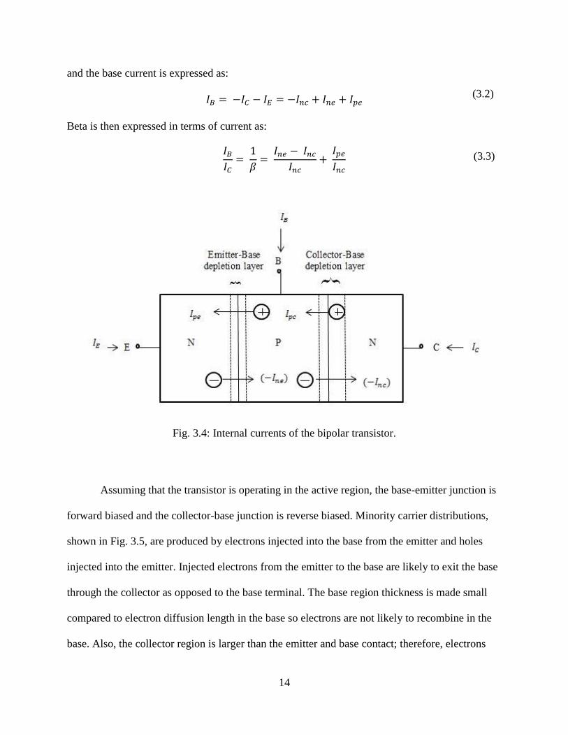
14
and the base current is expressed as:
𝐼𝐵 = −𝐼𝐶 − 𝐼𝐸 = −𝐼𝑛𝑐 + 𝐼𝑛𝑒 + 𝐼𝑝𝑒
Beta is then expressed in terms of current as:
𝐼𝐵
𝐼𝐶=
1
𝛽=
𝐼𝑛𝑒 − 𝐼𝑛𝑐
𝐼𝑛𝑐+
𝐼𝑝𝑒
𝐼𝑛𝑐
Fig. 3.4: Internal currents of the bipolar transistor.
Assuming that the transistor is operating in the active region, the base-emitter junction is
forward biased and the collector-base junction is reverse biased. Minority carrier distributions,
shown in Fig. 3.5, are produced by electrons injected into the base from the emitter and holes
injected into the emitter. Injected electrons from the emitter to the base are likely to exit the base
through the collector as opposed to the base terminal. The base region thickness is made small
compared to electron diffusion length in the base so electrons are not likely to recombine in the
base. Also, the collector region is larger than the emitter and base contact; therefore, electrons
(3.2)
(3.3)

15
diffusing away from the emitter have a higher probability of encountering the collector because
of the short distance from the emitter to collector [19].
There are three main requirements for large values of beta in a bipolar transistor:
1) heavy doping of the emitter,
2) long minority-carrier lifetimes in the base, and
3) short base thickness.
Fig. 3.5: Stored charge distribution in BJT normal active region.
For beta to have a large value, the internal current numerators of the terms in Eq. 3.3
need to be small in comparison to the 𝐼𝑛𝑐 denominator. The 𝐼𝑛𝑒 − 𝐼𝑛𝑐 term notes the difference
in electrons injected into the base at the base-emitter junction and the electrons swept across the
collector-base junction into the collector and is created by the recombination of some of the
injected electrons in the base region. This difference can be minimized by having increased
minority carrier lifetimes and shortening the thickness in the base region. The 𝐼𝑝𝑒 term can be
minimized by heavily doping the emitter so that the stored hole distribution becomes smaller.
These factors, however, conflict with other desirable device characteristics (such as
switching times) and trade-offs must be considered [19].
16
3.2.3 Output Characteristics
The typical output characteristics for a power bipolar transistor can be seen in Fig. 3.6.
The varying curves are distinguished by the values of the applied base current. The most notable
observable difference in the power bipolar transistor and its low-power logic-level counterpart is
the quasi-saturation region. Low-power transistors do not possess a drift region and therefore do
not exhibit the quasi-saturation effect; otherwise, the major transistor features are shared.
Quasi-saturation Region
One major difference between the power BJT and the low-power BJT is noted in the
saturation region seen in the output characteristics. The saturation region can, in fact, be
separated into two regions: “hard” saturation and “quasi-saturation” noted in Fig. 3.6. The quasi-
saturation effect, specific to power transistors, is noted as the gradual transition between the
saturation and forward active regions and is the result of introducing the lightly-doped drift
region, lacking in the low-power BJT structure. In the quasi-saturation region, the base-collector
junction is forward biased but excess minority carriers fail to short out the drift region; also,
resistivity in the region is affected by the base current. During quasi-saturation, the total drop in
voltage across the device is greater than that of saturation.
In the event of quasi-saturation, it is again assumed that the transistor is initially in the
active region. The collector-emitter voltage drops due to an increased voltage drop across the
collector load. This is caused by a rise in collector current in response to a rising base current.
There is, however, a simultaneous increase in the voltage drop in the drift region as a result of its
ohmic resistance due to the increase in 𝑖𝑐, meaning the reverse bias across the collector-base
junction is getting smaller and the junction will eventually become forward biased. Space charge

17
neutrality requires that electrons be injected into the drift region in approximately the same
proportion as the holes and electrons are obtained from the number of electrons being supplied to
the collector-base by injection from the emitter and diffusion across the base. Quasi-saturation
region is entered as the excess carrier build-up in the drift region ensues. If the ohmic resistance
of the drift region is 𝑅𝑑 and 𝑣𝐶𝐸 is the collector-emitter voltage, then the boundary between the
quasi-saturation region and the active region is given by:
𝑖𝐶 = 𝑣𝐶𝐸
𝑅𝑑
Fig. 3.6: Output characteristics of power transistor.
3.2.4 Switching Characteristics
Bipolar power transistors were developed for power circuit applications including motor
control. In these circuits, the device regulates the current being delivered to a load by serving as
a switch between the on- and off-states. The loads can be either resistive or inductive in nature.
Assuming an inductive load, the device switches from the blocking state to the on-state while
supporting the collector supply voltage, with a voltage drop during the turn-on transient. The
device switches from the on-state to the collector supply voltage during the turn-off transient.
These transitions determine the power losses incurred when the bipolar power transistor is
operated at high frequencies [15].
(3.4)

18
CHAPTER 4: SJT MODEL
4.1 Current State of SiC BJT/SJT Models
4.1.1 SiC BJT Models
Since the inception of the Si BJT, device models have been formulated to describe the
physical and electrical behavior. One of the first (Si) BJT models was developed by Ebers and
Moll in 1954 [20]. Though the mathematical simplicity of the model encourages ease of use, the
Ebers-Moll (EM) model neglects many effects that occur in BJTs. The GP model was introduced
in 1970 by Gummel and Poon [21]. It is the most used model (as it is built in to many simulators
such as HSPICE and Spectre) and addresses the effects that the EM model does not. Neither the
EM nor the GP models were designed for SiC devices. Recently, other more advanced BJT
models (though mostly for Si) have been used in the semiconductor industry, each with
advantages and shortcomings; while they, many of them being physics-based models, address
more device effects, longer simulation times are required. A main objective in device simulation
is to use the simplest model that will accurately complete the job. Integrated circuit design
heavily relies on compact device models for circuit simulation. The industry standard bipolar
transistor modeling is based on SPICE GP model (SPG). Though several limitations exist for
SGP model, few widely accepted alternatives are available to replace it. Several advanced
models, such as vertical bipolar inter-company (VBIC), high current (HICUM) and MEXTRAM
have been proposed and utilized [20-24].
With this in mind, it is useful to note some differences between current bipolar models. A
brief description and comparison a few models and the device characteristics they feature is
discussed.
The large signal equivalent circuits for all the models are in part based on the EM
transport model. All models include a transfer current source, diodes for both ideal and non-ideal
19
base current components, and series resistances.
In comparison to the SPG model (version Spice3G2), newer models’ large signal
equivalent circuits utilize a split B-E junction, split base resistance, a split B-C junction, a B-C
avalanche current model and a self-heating network. A more detailed comparison of the large
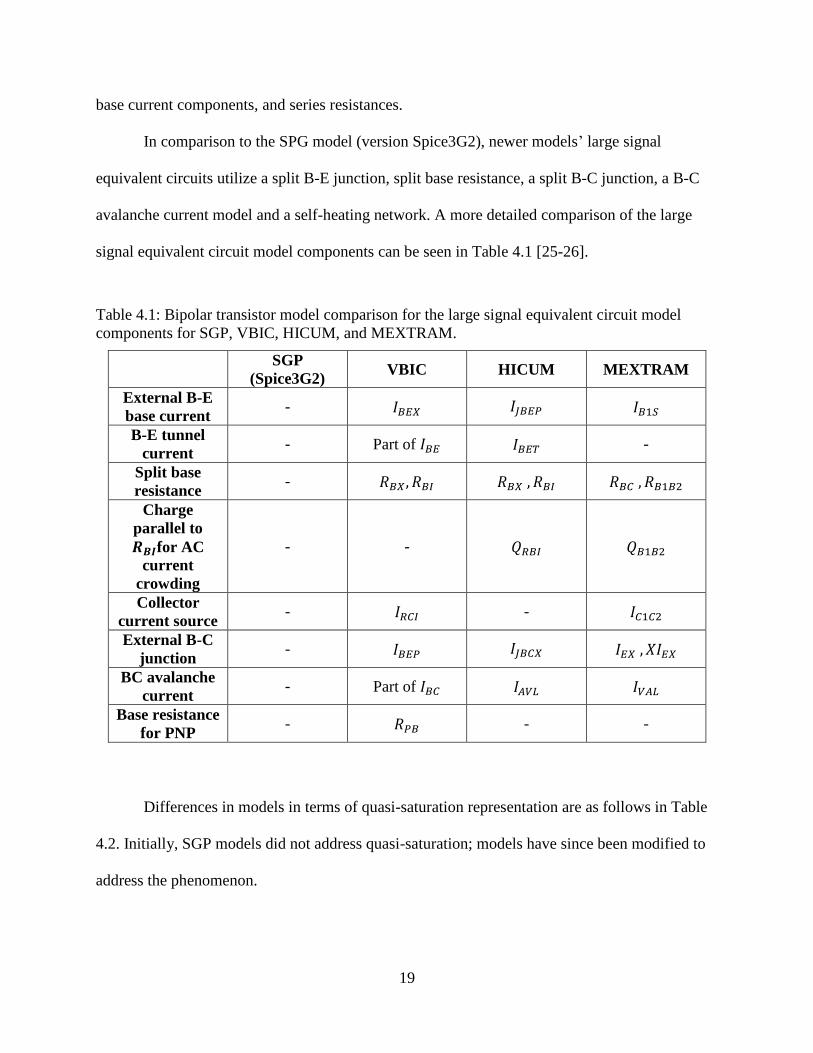
signal equivalent circuit model components can be seen in Table 4.1 [25-26].
Table 4.1: Bipolar transistor model comparison for the large signal equivalent circuit model
components for SGP, VBIC, HICUM, and MEXTRAM.
SGP
(Spice3G2) VBIC HICUM MEXTRAM
External B-E
base current - 𝐼𝐵𝐸𝑋 𝐼𝐽𝐵𝐸𝑃 𝐼𝐵1𝑆
B-E tunnel
current - Part of 𝐼𝐵𝐸 𝐼𝐵𝐸𝑇 -
Split base
resistance - 𝑅𝐵𝑋 , 𝑅𝐵𝐼 𝑅𝐵𝑋 , 𝑅𝐵𝐼 𝑅𝐵𝐶 , 𝑅𝐵1𝐵2
Charge
parallel to
𝑹𝑩𝑰for AC
current
crowding
- - 𝑄𝑅𝐵𝐼 𝑄𝐵1𝐵2
Collector
current source - 𝐼𝑅𝐶𝐼 - 𝐼𝐶1𝐶2
External B-C
junction - 𝐼𝐵𝐸𝑃 𝐼𝐽𝐵𝐶𝑋 𝐼𝐸𝑋 , 𝑋𝐼𝐸𝑋
BC avalanche
current - Part of 𝐼𝐵𝐶 𝐼𝐴𝑉𝐿 𝐼𝑉𝐴𝐿
Base resistance
for PNP - 𝑅𝑃𝐵 - -
Differences in models in terms of quasi-saturation representation are as follows in Table
4.2. Initially, SGP models did not address quasi-saturation; models have since been modified to
address the phenomenon.

20
Table 4.2: Quasi-saturation model comparison for SGP, VBIC, HICUM, and MEXTRAM.
Model Equation
SGP n/a
VBIC Quasi-saturation effect is modeled with the KULL-Model [25-26]
HICUM
Quasi-saturation effect is included in operating point dependency of the forward
minority charge 𝑄𝐹𝑇 [25-26]
MEXTRAM Quasi-saturation effect is modeled with a modified KULL-Model [25-27]
4.1.2 SiC SJT Models
While there are many Si BJT models available, there are few SiC BJT models. GeneSiC
Semiconductor utilizes a GP model for generic characterization of the unique SJT devices [28].
Because GeneSiC Semiconductor’s SJT device is fundamentally a [modified] BJT, this work
aims to present a modified GP model specifically for the characterization of a GeneSiC
Semiconductor 1700 V, 8 A junction transistor.
4.2 Model Description
The work presented is a compact model developed for the GeneSiC Semiconductor SiC
1700 V, 8 A SJT. The specific device is noted as GA08JT17-247. The model presented has been
written in Verilog-A modeling language and is supported by a variety of simulators and has been
implemented using a Berkeley Spice3f5 -based GP model. The basic structure of the model and
the equivalent circuit were adopted from a 1200 V, 6 A SiC BJT model developed at the
Zhejiang University in Hangzhou, China [29] and can be seen in Fig. 4.1. Throughout this work
description, the model parameters have been written in all-capital bold letters (such as BF) and
21
constant values and calculated variables are written with the italicized name of the variable (such
as 𝑉𝐵𝐶). Temperature scaled values are noted with a subscript T (such as 𝐁𝐅𝐓).
The software used for the development of the model was a tool, developed at the
University of Arkansas, titled Paragon 2. The Paragon 2 software enables the capture of
equations, data, curves, variables, and expressions, all in a graphical form allowing the program
to utilize models in a variety of languages [2].
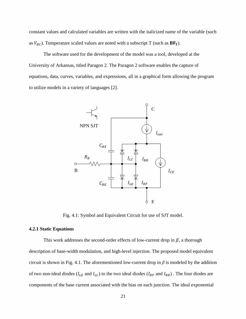
Fig. 4.1: Symbol and Equivalent Circuit for use of SJT model.
4.2.1 Static Equations
This work addresses the second-order effects of low-current drop in 𝛽, a thorough
description of base-width modulation, and high-level injection. The proposed model equivalent
circuit is shown in Fig. 4.1. The aforementioned low-current drop in β is modeled by the addition
of two non-ideal diodes (𝐼𝐿𝐸 and 𝐼𝐿𝐶) to the two ideal diodes (𝐼𝐵𝐹 and 𝐼𝐵𝑅) . The four diodes are
components of the base current associated with the bias on each junction. The ideal exponential
E
𝐼𝐿𝐶
𝐼𝐵𝐹
𝐼𝐵𝑅
𝐼𝐿𝐸
𝐼𝑒𝑝𝑖
𝐶𝐵𝑋
𝐶𝐵𝐸
𝑅𝐵
NPN SJT
B
C
𝐼𝐶𝐸

22
current term, 𝐼𝐵𝐹, accounts for the recombination in the inactive base region and carriers injected
into the emitter. Non-ideal exponential voltage term,𝐼𝐿𝐸, is predominant at lower biases caused
by recombination in the emitter junction spaced charge region; likewise for emission and
recombination near the collector junction, represented by 𝐼𝐵𝑅 and 𝐼𝐿𝐶.
The four total diodes currents (𝐼𝐵𝐹 , 𝐼𝐵𝑅 , 𝐼𝐿𝐸 , 𝐼𝐿𝐶 ) are represented by the following
equations[17-18] [20]:
𝐼𝐵𝐹 = 𝐈𝐒
𝐁𝐅(𝑒𝑞𝑉𝐵𝐸 𝐍𝐅𝑘𝐓⁄ − 1)
𝐼𝐵𝑅 = 𝐈𝐒
𝐁𝐑(𝑒𝑞𝑉𝐵𝐶 𝐍𝐑𝑘𝐓⁄ − 1)
𝐼𝐿𝐸 = 𝐈𝐒𝐄(𝑒𝑞𝑉𝐵𝐶 𝐍𝐄𝑘𝐓⁄ − 1)
𝐼𝐿𝐶 = 𝐈𝐒𝐂(𝑒𝑞𝑉𝐵𝐶 𝐍𝐂𝑘𝐓⁄ − 1)
where q is the electron charge, k is Boltzmann’s constant and T is the user-defined temperature
parameter.
The saturation current is noted by IS and the non-ideal base-emitter and base-collector
saturation currents are defined as ISE and ISC, respectively. These are variations of standard
diode equations with the addition of forward and reverse current emission coefficient parameters,
NF and NR, and non-ideal low-current base-emitter and base-collector emission coefficients, NE
and NC. In addition to these parameters, the diode current equations are exponentially dependent
on the base-collector and base-emitter voltages 𝑉𝐵𝐸 and 𝑉𝐵𝐶 [16-17].
(4.1)
(4.2)
(4.3)
(4.4)

23
Early Effect
The Early effect is another characteristic specifically described in this model. The
collector current increases with an increase in the collector-emitter voltage, and therefore also an
increase in the collector-base voltage, caused by the effective shortening of the base width due to
the depletion-layer expansion. The effect is described inside the model with the addition of
forward Early voltage and reverse Early voltage parameters, VAF and VAR, which can be seen
within the equations for variables 𝑞1𝑠 and 𝑞2𝑠 as components of base charge factor, 𝑛𝑞𝑏.
High Level Injection Effect
High level injection in the bipolar transistor occurs when the injected minority carrier
concentration in the base region is larger than the doping concentration when the device is
operating at high current densities. To satisfy charge neutrality, majority carrier concentration in
the base increases under high-level injection conditions, enhancing the injection of holes from
the base into the emitter. This reduces injection efficiency and current gain of the device.
The parameters IKF and IKR are added to address high-level injection in the collector and base
and represent forward- and reverse-beta high-current roll-off. [16-17].
𝑛𝑞𝑏 =𝑞1𝑠
2∗ (1 + √1 + 4𝑞2𝑠 )
where
𝑞1𝑠 = 1 (1 −𝑉𝐵𝐶
𝐕𝐀𝐅−
𝑉𝐵𝐸
𝐕𝐀𝐑)⁄
and
𝑞2𝑠 = 𝐼𝐵𝐹
𝐈𝐊𝐅+
𝐼𝐵𝑅
𝐈𝐊𝐑
(4.5)
(4.6)
(4.7)

24
The base and collector terminal currents are then mathematically represented as follows[17]:
𝐼𝐶 =𝐼𝐵𝐹 − 𝐼𝐵𝑅
𝑛𝑞𝑏−
𝐼𝐵𝑅
𝐁𝐑𝐓− 𝐼𝐿𝐶
𝐼𝐵 = 𝐼𝐵𝐹
𝐁𝐅𝐓+ 𝐼𝐿𝐸 +
𝐼𝐵𝑅
𝐁𝐑𝐓+ 𝐼𝐿𝐶
where 𝐁𝐅𝐓 and 𝐁𝐑𝐓 are user-defined ideal forward- and reverse-current gains (β).
This work also takes into account the current dependence of the base resistance. The base
resistance rests between the external and internal base nodes and consists of two separate
resistances noted by parameters RB and RBM. RB represents the extrinsic base resistance made
of the contact resistance and sheet resistance of the external base region. RBM is the intrinsic
resistance of the internal base region, lying directly underneath the emitter. The total base
resistance is represented in Eq. 4.10 as follows:
𝑅𝐵 = 𝐑𝐁𝐌 + 3(𝐑𝐁 − 𝐑𝐁𝐌) (tan 𝑧 − 𝑧
𝑧 tan2 𝑧)
where
𝑧 = −1 + √1 + 144𝐼𝐵 𝜋2𝐈𝐑𝐁⁄
(24 𝜋2⁄ )√𝐼𝐵 𝐈𝐑𝐁⁄
and IRB is the current where the base resistance halfway to its minimum value.
4.2.2 Quasi-Saturation Model
The quasi-saturation effect is the gradual transition between the saturation region and the
forward active region of a bipolar transistor. In this model, the quasi-saturation effects are
accounted for by describing the collector resistance as shown in Eq. 4.12 [23]. The variable 𝑉𝐵𝑋
represents the voltage flowing from internal base node to the external collector node and the
value of 4𝑛𝑖2
𝐍𝐄𝐏𝐈2 is commonly noted as gamma (𝛾𝑒𝑝𝑖), where 𝑛𝑖 is the intrinsic carrier
(4.8)
(4.9)
(4.10)
(4.11)

25
concentration and 𝐍𝐄𝐏𝐈 is the epitaxial impurity concentration, and 𝐑𝐂𝐎 is the zero bias
collector series resistance.
𝑅𝐶 =𝐑𝐂𝐎
12 +
14
√1 +4𝑛𝑖2
𝐍𝐄𝐏𝐈2 exp(𝑞𝑉𝐵𝐶 𝑘𝐓⁄ ) +14
√1 +4𝑛𝑖2
𝐍𝐄𝐏𝐈2 exp(𝑞 𝑉𝐵𝑋 𝑘𝐓⁄ )
The quasi-saturation model is based on a model created by G.M. Kull and L.W. Nagel in
1985 [22]. The quasi-saturation effect is modeled by the epitaxial current source, 𝐼𝑒𝑝𝑖, as seen in
Fig. 4.1 and is described by the following equation:
𝐼𝑒𝑝𝑖 =𝐹𝑖 − 𝐹𝑥 − 𝑙𝑛 (
1 + 𝐹𝑖
1 + 𝐹𝑥) +
𝑞(𝑉𝐵𝐶− 𝑉𝐵𝑋)𝐄𝐏𝐗𝐂𝐎 𝑘 𝐓
𝑞 𝑅𝐶
𝐄𝐏𝐗𝐂𝐎 𝑘 𝐓 (
|𝑉𝐵𝐶 − 𝑉𝐵𝑋|𝐕𝐎 )
where 𝐹𝑖 and 𝐹𝑥 are variables described as follows:
𝐹𝑖 = [1 + 𝛾𝑒𝑝𝑖𝑒𝑞𝑉𝐵𝐶 𝐄𝐏𝐗𝐂𝐎𝑘𝐓⁄ ]
1 2⁄
𝐹𝑥 = [1 + 𝛾𝑒𝑝𝑖𝑒𝑞𝑉𝐵𝑋 𝐄𝐏𝐗𝐂𝐎𝑘𝐓⁄ ]
1 2⁄
In Eq. 4.13 𝐄𝐏𝐗𝐂𝐎 notes the epitaxial region emission coefficient and 𝑅𝐶 is the series resistance
adopted from [23], shown in Eq. 4.12, and 𝐕𝐎 is the carrier velocity saturation voltage [16].
4.2.3 Dynamic Equations
Two depletion capacitors can be used to model the incremental fixed charges stored in
the depletion regions of the bipolar transistor for changes in the associated junction voltages.
Each junction capacitance is a nonlinear function of change in voltage across its respective
junction. Because both the base-emitter and base-collector junctions are not forward biased
heavily in normal condition, the capacitance model proposed in [20] and used for this work
neglects the capacitance due to diffusion capacitances. Therefore, the junction capacitances
(𝐶𝐵𝐸 and 𝐶𝐵𝑋) and respective charges (𝑄𝐵𝐸 and 𝑄𝐵𝑋) are represented as follows [20]:
(4.14)
(4.15)
(4.12)
(4.13)

26
𝑄𝐵𝐸 = 𝐂𝐉𝐄 ∫ (1 −𝑉
𝐕𝐉𝐄)
−𝐌𝐄𝑉𝐵𝐸
0
dV
𝐶𝐵𝐸 =𝐂𝐉𝐄
(1 −𝑉𝐵𝐸
𝐕𝐉𝐄⁄ )𝐌𝐄
𝑄𝐵𝑋 = 𝐂𝐉𝐂(1 − 𝑿𝑪𝑱𝑪) ∫ (1 −𝑉
𝐕𝐉𝐂)
−𝐌𝐂𝑉𝐵𝑋
0
dV
𝐶𝐵𝑋 =𝐂𝐉𝐂(𝟏 − 𝑿𝑪𝑱𝑪)
(1 −𝑉𝐵𝑋
𝐕𝐉𝐂⁄ )𝐌𝐂
for 𝑉𝐵𝐸 < 𝐅𝐂 × 𝐕𝐉𝐄 and 𝑉𝐵𝑋 < 𝐅𝐂 × 𝐕𝐉𝐂, and:
𝑄𝐵𝐸 = 𝐂𝐉𝐄 𝐹1 +𝐂𝐉𝐄
𝐹2∫ (𝐹3 +
𝐌𝐄 𝑉
𝐕𝐉𝐄)
𝑉𝐵𝐸
𝐅𝐂 ×𝐕𝐉𝐄
dV
𝐶𝐵𝐸 = 𝐂𝐉𝐄
𝐹2(𝐹3 +
𝐌𝐄 𝑉𝐵𝐸
𝐕𝐉𝐄)
𝑄𝐵𝑋 = 𝐂𝐉𝐂(1 − 𝐗𝐂𝐉𝐂) 𝐹1 +𝐂𝐉𝐂(1 − 𝐗𝐂𝐉𝐂)
𝐹2∫ (𝐹3 +
𝐌𝐂 𝑉
𝐕𝐉𝐂)
𝑉𝐵𝑋
𝐅𝐂 ×𝐕𝐉𝐂
dV
𝐶𝐵𝑋 = 𝐂𝐉𝐂(1 − 𝐗𝐂𝐉𝐂)
𝐹2(𝐹3 +
𝐌𝐂 𝑉𝐵𝑋
𝐕𝐉𝐂)
for 𝑉𝐵𝐸 ≥ 𝐅𝐂 × 𝐕𝐉𝐄 and 𝑉𝐵𝑋 ≥ 𝐅𝐂 × 𝐕𝐉𝐂, where:
𝐹1 = 𝐕𝐉𝐄
1−𝐌𝐄[1 − (1 − 𝐅𝐂)1−𝐌𝐄]
𝐹2 = (1 − 𝐅𝐂)1+𝐌𝐄
𝐹3 = 1 − 𝐅𝐂(1 + 𝐌𝐄)
for the base-emitter junction, and:
𝐹1 = 𝐕𝐉𝐂
1 − 𝐌𝐂[1 − (1 − 𝐅𝐂)1−𝐌𝐂]
𝐹2 = (1 − 𝐅𝐂)1+𝐌𝐂
𝐹3 = 1 − 𝐅𝐂(1 + 𝐌𝐂)
for the base-collector junction.
(4.22)
(4.21)
(4.19)
(4.16)
(4.17)
(4.20)
(4.23)
(4.24)
(4.25)
(4.26)
(4.27)
(4.28)
(4.29)
(4.18)

27
CJE and CJC represent the values of the zero-biased capacitance parameters at the base-
emitter and base-collector junctions. The built in potential parameters are noted by VJE and
VJC and the pn grading factor parameters ME and MC. Parameter FC is the coefficient for
forward-bias depletion capacitance used to compute the voltage in the forward-biased region,
𝐅𝐂 × 𝐕𝐉𝐄 and 𝐅𝐂 × 𝐕𝐉𝐂, respectively, and is valued between zero and one. An approximation of
the distributed resistance and capacitance at the base collector junction is addressed in this model
with the capacitance between the internal base and external collector (CBX). Parameter 𝐗𝐂𝐉𝐂
specifies the ratio between the separation of junction capacitance at the base-collector junction
and ranges between zero and one [17].
4.3 Temperature Scaling
Initial data for the model is assumed to have been taken at approximately 25 °C.
However, the model allows for users to view device behavior across a range of temperatures.
This work simulates device behavior from 25 °C to 175 °C, adjusting the simulation temperature
by changing the value of parameter T.
In order to reflect changes in temperature, some device parameter and variable equations
are modified. These parameters, variables, and their temperature dependent equations can be
seen in Table 4.3. In the following equations, 𝑇1 is the default nominal temperature, 25 °C, and
𝑇2 represents the newly user-specified simulation temperature created by changing parameter T.
28
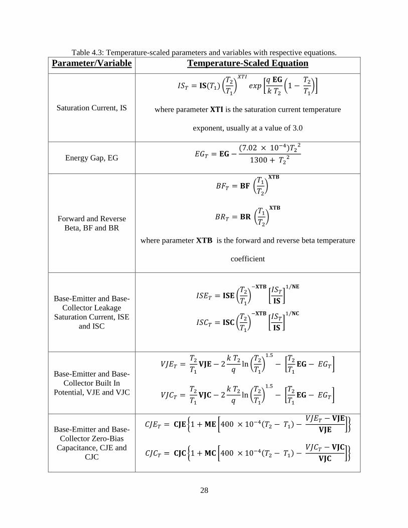
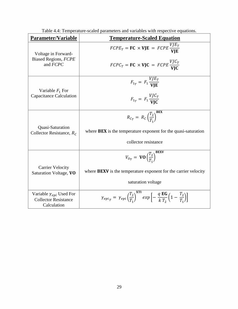
Table 4.3: Temperature-scaled parameters and variables with respective equations.
Parameter/Variable Temperature-Scaled Equation
Saturation Current, IS
𝐼𝑆𝑇 = 𝐈𝐒(𝑇1) (𝑇2
𝑇1)
𝑋𝑇𝐼
𝑒𝑥𝑝 [𝑞 𝐄𝐆
𝑘 𝑇2(1 −
𝑇2
𝑇1)]
where parameter 𝐗𝐓𝐈 is the saturation current temperature
exponent, usually at a value of 3.0
Energy Gap, EG 𝐸𝐺𝑇 = 𝐄𝐆 −
(7.02 × 10⁻⁴)𝑇22
1300 + 𝑇22
Forward and Reverse
Beta, BF and BR
𝐵𝐹𝑇 = 𝐁𝐅 (𝑇1
𝑇2)
𝐗𝐓𝐁
𝐵𝑅𝑇 = 𝐁𝐑 (𝑇1
𝑇2)
𝐗𝐓𝐁
where parameter XTB is the forward and reverse beta temperature
coefficient
Base-Emitter and Base-
Collector Leakage
Saturation Current, ISE
and ISC
𝐼𝑆𝐸𝑇 = 𝐈𝐒𝐄 (𝑇2
𝑇1)
−𝐗𝐓𝐁
[𝐼𝑆𝑇
𝐈𝐒]
1 𝐍𝐄⁄
𝐼𝑆𝐶𝑇 = 𝐈𝐒𝐂 (𝑇2
𝑇1)
−𝐗𝐓𝐁
[𝐼𝑆𝑇
𝐈𝐒]
1 𝐍𝐂⁄
Base-Emitter and Base-
Collector Built In
Potential, VJE and VJC
𝑉𝐽𝐸𝑇 = 𝑇2
𝑇1𝐕𝐉𝐄 − 2
𝑘 𝑇2
𝑞ln (
𝑇2
𝑇1)
1.5
− [𝑇2
𝑇1𝐄𝐆 − 𝐸𝐺𝑇]
𝑉𝐽𝐶𝑇 = 𝑇2
𝑇1𝐕𝐉𝐂 − 2
𝑘 𝑇2
𝑞ln (
𝑇2
𝑇1)
1.5
− [𝑇2
𝑇1𝐄𝐆 − 𝐸𝐺𝑇]
Base-Emitter and Base-
Collector Zero-Bias
Capacitance, CJE and
CJC
𝐶𝐽𝐸𝑇 = 𝐂𝐉𝐄 1 + 𝐌𝐄 [400 × 10−4(𝑇2 − 𝑇1) − 𝑉𝐽𝐸𝑇 − 𝐕𝐉𝐄
𝐕𝐉𝐄]
𝐶𝐽𝐶𝑇 = 𝐂𝐉𝐂 1 + 𝐌𝐂 [400 × 10−4(𝑇2 − 𝑇1) − 𝑉𝐽𝐶𝑇 − 𝐕𝐉𝐂
𝐕𝐉𝐂]
29
Table 4.4: Temperature-scaled parameters and variables with respective equations.
Parameter/Variable Temperature-Scaled Equation
Voltage in Forward-
Biased Regions, FCPE
and FCPC
𝐹𝐶𝑃𝐸𝑇 = 𝐅𝐂 × 𝐕𝐉𝐄 = 𝐹𝐶𝑃𝐸𝑉𝐽𝐸𝑇
𝐕𝐉𝐄
𝐹𝐶𝑃𝐶𝑇 = 𝐅𝐂 × 𝐕𝐉𝐂 = 𝐹𝐶𝑃𝐸𝑉𝐽𝐶𝑇
𝐕𝐉𝐂
Variable 𝐹1 For
Capacitance Calculation
𝐹1𝑇= 𝐹1
𝑉𝐽𝐸𝑇
𝐕𝐉𝐄
𝐹1𝑇= 𝐹1
𝑉𝐽𝐶𝑇
𝐕𝐉𝐂
Quasi-Saturation
Collector Resistance, 𝑅𝐶
𝑅𝐶𝑇= 𝑅𝐶 (
𝑇2
𝑇1)
𝐁𝐄𝐗
where 𝐁𝐄𝐗 is the temperature exponent for the quasi-saturation
collector resistance
Carrier Velocity
Saturation Voltage, 𝐕𝐎
𝑉𝑂𝑇= 𝐕𝐎 (
𝑇2
𝑇1)
𝐁𝐄𝐗𝐕
where 𝐁𝐄𝐗𝐕 is the temperature exponent for the carrier velocity
saturation voltage
Variable 𝛾𝑒𝑝𝑖 Used For
Collector Resistance
Calculation
𝛾𝑒𝑝𝑖 𝑇= 𝛾𝑒𝑝𝑖 (
𝑇2
𝑇1)
𝐗𝐓𝐈
𝑒𝑥𝑝 [− 𝑞 𝐄𝐆
𝑘 𝑇2(1 −
𝑇2
𝑇1)]
30
CHAPTER 5: MODEL SIMULATION AND VERIFICATION
This chapter provides the simulated and verified results of the GeneSiC 1.7 kV, 8 A SiC
SJT from the model presented in this work. Model verification consists of validating the model
with real device data. The model must be mathematically accurate and properly formulated for
accurate simulation results and for convergence under different bias conditions. Verification also
includes affirmation of model convergence and satisfactory simulation times.
Evaluating Model Performance
Selected parameter values for the GA08JT17-247 1.7 kV, 8 A SiC power super junction
transistors are available on the GeneSiC Semiconductor website [28]; however, these parameter
values are for standard bipolar models. Super junction device data measurements were taken
from the GA08JT17-247 datasheet, as well as C-V and switching measurements provided from
GeneSiC, for the evaluation of model performance through comparison of simulated results to
measured data. For model validation, simulated results should be reasonably accurate against
measured data. Simulation and parameter extraction for the output characteristics and C-V
curves were performed in IC-CAP, an industry standard modeling tool. Switching characteristics
were simulated in Paragon 2 as IC-CAP does not support switching analysis.
5.1 Parameter Extraction and Simulation Analysis
5.1.1 Parameter Extraction
The presented model was developed in a manner that allows for parameter extraction
using available device datasheets. There are nominal parameters and temperature-dependent
parameters that affect the scaling of the nominal parameters. Parameter extraction often consists

31
of three main steps: taking physical device measurements (or digitizing data from a datasheet),
extraction of parameters at room temperature, and then extraction of temperature scaled
parameters. The parameter extraction strategy for this work was followed by using data from the
GA08JT17-247 device datasheet. Data presented in datasheets are often mean-valued data sets
and variation in data from one device to another is expected.
It is generally easier to extract model parameters in groups; for example, extracting DC
parameters, ohmic parasitics, and C-V parameters. Each parameter group then becomes the
initial condition for each extraction step thereafter.
Though IC-CAP includes a built-in parameter extraction and optimization sequence, the
presented work extracted parameters manually starting with initial values identified from the
GeneSiC GA08JT17-247 datasheet seen in Table 5.
Table 5.1: Parameter values for GA08JT17-247 device model.
Parameter
Definition
GeneSiC
Datasheet
Initial Value
(25 °C)
Extracted Parameter Values
25 °C 125 °C 175 °C
IS Transport saturation
current 3.73E-47 (A) 3.49 E-47 3.77 E-42 3.29 E-26
BF Ideal maximum forward
beta 63 63 55 55.0
BR Ideal maximum reverse
beta 0.55 0.552 0.350 0.632
NR Reverse current emission
coefficient - 1.048 0.670 0.713
NF Forward current emission
coefficient 1.0 1.095 0.670 0.707
IKF
Forward-beta high-
current roll-off “knee”
current
200.0 (A) 250.0 275 200.0
IKR
Reverse-beta high-
current roll-off “knee”
current
- (A) 100 100 100

32
Table 5.1: Parameter values for GA08JT17-247 device model, cont’d.
Parameter
Definition
GeneSiC
Datasheet
Initial Value
(25 °C)
Extracted Parameter Values
25 °C 125 °C 175 °C
ISE Base-emitter leakage
saturation current 5.50E-27 (A) 6.91 E-27 1.74 E-23 59.7 E-15
NE Base-emitter leakage
emission coefficient 2.201 2.425 2.195 3.065
ISC Base-collector leakage
saturation current - (A) 8.38 E-27 3.48 E-23 42.9 E-18
NC Base-collector leakage
emission coefficient - 2.250 2.0 1.497
VAR Reverse Early voltage - (V) 150.0 100.0 10.0
VAF Forward Early voltage - (V) 265.0 90.0 75.0
RCO Zero-bias collector series
resistance - (ohm) 0.212 0.097 0.198
NEPI Epitaxial impurity
concentration - 2.75 E14 115 E14 1.39 E14
VO Carrier velocity
saturation voltage - (V) 14 6.380 6.231
EPXCO Epitaxial region emission
coefficient - 1.0 1.0 1.0
BEX Temperature exponent
for RCO - 2.42 4.975 2.277
BEXV Temperature exponent
for VO - 1.9 3.0 1.618
RB Zero-bias (maximum)
base resistance 6.0 (ohm) 4.146 4.146 4.146
RBM Minimum base resistance 0.9 (ohm) 0.166 0.166 0.166
IRB
Current where base
resistance equals
(RB+RBM)/2
1.0E-4 (A) 56.2 E-6 56.2 E-6 56.2 E-6
CJE Base-emitter zero-bias
capacitance 8.23E-10 (F) 8.22 E-10 8.22 E-10 8.22 E-10
VJE Base-emitter built-in
potential 2.945 (V) 2.837 2.837 2.837
MJE Base-emitter grading
factor 0.498 0.4862 0.4862 0.4862
FC Forward-bias depletion
capacitor coefficient - 0.6941 0.6941 0.6941
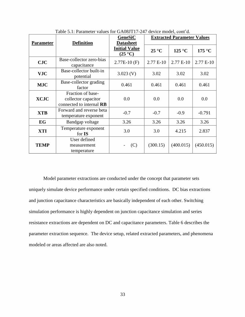
33
Table 5.1: Parameter values for GA08JT17-247 device model, cont’d.
Parameter
Definition
GeneSiC
Datasheet
Initial Value
(25 °C)
Extracted Parameter Values
25 °C 125 °C 175 °C
CJC Base-collector zero-bias
capacitance 2.77E-10 (F) 2.77 E-10 2.77 E-10 2.77 E-10
VJC Base-collector built-in
potential 3.023 (V) 3.02 3.02 3.02
MJC Base-collector grading
factor 0.461 0.461 0.461 0.461
XCJC
Fraction of base-
collector capacitor
connected to internal RB
0.0 0.0 0.0 0.0
XTB Forward and reverse beta
temperature exponent -0.7 -0.7 -0.9 -0.791
EG Bandgap voltage 3.26 3.26 3.26 3.26
XTI Temperature exponent
for IS 3.0 3.0 4.215 2.837
TEMP
User defined
measurement
temperature
- (C) (300.15) (400.015) (450.015)
Model parameter extractions are conducted under the concept that parameter sets
uniquely simulate device performance under certain specified conditions. DC bias extractions
and junction capacitance characteristics are basically independent of each other. Switching
simulation performance is highly dependent on junction capacitance simulation and series
resistance extractions are dependent on DC and capacitance parameters. Table 6 describes the
parameter extraction sequence. The device setup, related extracted parameters, and phenomena
modeled or areas affected are also noted.

34
Table 5.2: Device setup, related extracted parameters, and phenomena modeled or areas affected
for parameter extraction sequence.
Sequence Characteristic Measurement Parameter Phenomenon Modeled
or Area Affected
1 DC Large Signal
Forward Bias
𝐼𝐶 𝑣𝑠 𝑉𝐶𝐸
IS Hard saturation region of
output curves
BF Low level non-ideal currents/
spacing between output
family of curves
𝐼𝐵 𝑣𝑠 𝑉𝐵𝐸 IKF
Variation in forward beta at
high collector currents/
“knee” of curve in Forward
Gummel plots
𝐼𝐶 𝑣𝑠 𝑉𝐶𝐸
NF Deviation of emitter base
diode from ideal
ISE Variation of forward beta at
low base currents
NE Variation of forward beta at
low base currents
VAF Forward Early voltage/ base
collector bias on forward
beta and saturation current
1 DC Large Signal
Reverse Bias
𝐼𝐶 𝑣𝑠 𝑉𝐶𝐸 BR Low level non-ideal
currents/Saturation and
reverse regions
𝐼𝐵 𝑣𝑠 𝑉𝐵𝐸 IKR
Variation in reverse beta at
high emitter currents/ “knee”
current at reverse beta high-
current roll-off
𝐼𝐶 𝑣𝑠 𝑉𝐶𝐸
NR Deviation of base collector
diode from ideal
ISC
Variation in reverse beta at
low base currents/models
base current at low base-
collector voltage
𝐼𝐶 𝑣𝑠 𝑉𝐶𝐸
NC
Variation in reverse beta at
low base currents/models
base current at low base-
collector voltage
VAR
Reverse Early
voltage/emitter base bias on
reverse beta and saturation
current

35
Table 5.2: Device setup, related extracted parameters, and phenomena modeled or areas affected
for parameter extraction sequence, cont’d.
Sequence Characteristic Measurement Parameter Phenomenon Modeled
or Area Affected
2 Quasi-Saturation
Model 𝐼𝐶 𝑣𝑠 𝑉𝐶𝐸
RCO Hard and Quasi-saturation
regions
NEPI Hard and Quasi-saturation
regions
VO Hard and Quasi-saturation
regions
EPXCO Hard and Quasi-saturation
regions
BEX Hard and Quasi-saturation
regions
BEXV Hard and Quasi-saturation
regions
3 Series Resistance 𝐼𝐵 𝑣𝑠 𝑉𝐵𝐸
RB Parasitic resistance in base
RBM Variation in base resistance
as base current varies
IRB
4
Junction
Capacitance
𝐶𝐵𝐸 𝑣𝑠 𝑉𝐵𝐸 and
𝐶𝐵𝐸
+ 𝐶𝐵𝐶 𝑣𝑠 𝑉𝐶𝐸
CJE Base-emitter
capacitance/switching times
VJE Base-emitter capacitance
variation with bias
MJE Base-emitter capacitance
variation with bias
𝐶𝐵𝐶 𝑣𝑠 𝑉𝐶𝐸 and
𝐶𝐵𝐸
+ 𝐶𝐵𝐶 𝑣𝑠 𝑉𝐶𝐸
CJC Base-collector
capacitance/switching times
VJC Base-collector capacitance
variation with bias
𝐶𝐵𝐸 𝑣𝑠 𝑉𝐵𝐸,
𝐶𝐵𝐸 +𝐶𝐵𝐶 𝑣𝑠 𝑉𝐶𝐸
and
𝐶𝐵𝐶 𝑣𝑠 𝑉𝐶𝐸
MJC Base-collector capacitance
variation with bias
FC Provides continuity between
forward and reverse biased
capacitance
5 Temperature
Effects All
XTB Variation of beta with
temperature
EG
Energy gap for modeling
temperature
effects/temperature variation
of saturation currents in
collector and base-emitter
and collector-base diodes
XTI Variation of saturation
current with temperature

36
5.1.2 Simulation Results and Verification
For the simulated results presented in this work, corresponding data was provided from
GeneSiC Semiconductor across the following conditions at room temperature:
Setup 1: Output characteristics ( 𝐼𝐶 𝑣𝑠 𝑉𝐶𝐸 )
𝐼𝐵 is swept from 0 mA to 300 mA in steps of 100 mA
𝑉𝐶𝐸 is swept from 0 V to 5.9 V in steps of 50 mV
Setup 2: C-V characteristics ( 𝐶𝐵𝐸 𝑣𝑠 𝑉𝐵𝐸 ) and ( 𝐶𝐵𝐶 𝑣𝑠 𝑉𝐶𝐸 )
𝑉𝐵𝐸 is swept from -10 V to 3.3 V in steps of 10 mV
𝑉𝐶𝐸 is swept from 0 V to 1 kV in steps of 1 V
Setup 3: Switching characteristics (Turn-off and Turn-on)
Ideal resistive load circuit with varying user-defined added parasitics.
The output characteristics were simulated by application of a base current. The voltage
across the collector and emitter was swept and the current at the collector terminal was
measured. The reference circuit for the output characteristics is seen in Fig. 5.1a. The base-
emitter C-V simulation was achieved by measuring the capacitance across the base-emitter
terminals while sweeping a voltage across the base-emitter terminals. Likewise, base-collector
C-V simulations were achieved by measuring the base-collector capacitance and the sum of the
base-emitter and base-collector capacitances, respectively, while sweeping a voltage across the
base-collector terminals. Accurate fitting of the C-V data is essential for accuracy in switching
verification. The switching characteristics were captured with use of an ideal resistive load
schematic noted in Fig. 5.1d. Parasitic inductances and other passives will be specific to mimic
the user testbench schematic in order to introduce ringing for a more practical simulation.
Variations of measurement conditions to account for temperature scaling are as follows:

37
Setup 1: Output characteristics for 125 °C ( 𝐼𝐶 𝑣𝑠 𝑉𝐶𝐸 )
𝐼𝐵 is swept from 0 mA to 1 A in steps of 200 mA
𝑉𝐶𝐸 is swept from 0 V to 8.5 V in steps of 50 mV
Setup 1: Output characteristics for 175 °C ( 𝐼𝐶 𝑣𝑠 𝑉𝐶𝐸 )
𝐼𝐵 is swept from 0 mA to 1 A in steps of 200 mA
𝑉𝐶𝐸 is swept from 0 V to 15 V in steps of 50 mV
Setup 2 and 3: C-V characteristics and Switching characteristics (Turn-off and Turn-on)
Displayed negligible effects during temperature variation
Fig. 5.1: Simulation test bench circuits used for (a) output characteristics (b) base-emitter C-V
(c) base-collector C-V and (d) switching simulations.
(a) (b)
(c)
(d)
(d)

38
In order to verify the model, values from the GA08JT17-247 datasheet and, released
technical articles, were digitized and used in comparison to simulated results [28]. The model
parameters were then adjusted from their initial values to ensure optimal agreement against the
digitized measured data.
Output Characteristics
The simulated and measured output characteristics of the SJT at 25 °C are shown in Fig.
5.2. For simulation, base currents of 0 mA, 100 mA, 200 mA, and 300 mA were applied to the
base terminal, the collector-emitter terminal voltage (𝑉𝐶𝐸) was swept from 0 V to 5.9 V, and the
collector current (𝐼𝐶 ) was measured and plotted against 𝑉𝐶𝐸 using the circuit shown in Fig. 5.1a
.
Fig. 5.2: SJT output characteristics at room temperature (25 ˚C).
-2
0
2
4
6
8
10
12
14
16
18
20
0 1 2 3 4 5 6 7
Co
llec
tor
Cu
rren
t, I
c (A
)
Collector-Emitter Voltage, Vce (V)
0 mA
100 mA
200 mA
300 mAMeasured
Simulated
39
The family of curves show close agreement between the measured and simulated data.
The linear region is accurately represented in both hard and quasi-saturation. Overall, the family
of curves for the output characteristics at 25 °C is considered a good fit.
C-V Characteristics
Base-Emitter Capacitance
In order to verify the C-V simulation capabilities of the proposed model, measured data
of the C-V characteristics was provided by GeneSiC Semiconductor and compared to simulated
results. Simulation of the base-emitter C-V characteristics were obtained by applying a voltage
across the base-emitter terminals, swept from -10 V to 3.3 V and measuring the capacitance
across the base-emitter terminals; the simulation testbench circuit is noted in Fig. 5.1b. The
results for the base-emitter C-V characteristics are given in Fig. 5.3a.
The simulated C-V curve for the base-emitter junction shows an extremely good fit when
verified against the measured data. Nearly seamless simulation is noted until close to 2 V
confirming simulation performance acceptance.
Base-Collector Capacitance
Simulation of the base-collector C-V characteristics were obtained by applying a voltage
across the collector-emitter terminals, swept from 0 V to 1 kV and measuring capacitance across
base-collector terminals; simulation testbench is noted in Fig. 5.1c and the results for the base-
collector C-V characteristics are shown in Fig. 5.3b. An excellent fit was obtained when verified
against the measured data.

40
Fig. 5.3: (a) Base-emitter and (b) base-collector C-V characteristics.
Measured
Simulated
0
5E-11
1E-10
1.5E-10
2E-10
2.5E-10
3E-10
0 200 400 600 800 1000 1200
Base
-Co
llec
tor
Ca
pa
cita
nce
, C
bc
(F)
Collector-Emitter Voltage, Vce (V)
Meausured
Simulated
0E+00
5E-10
1E-09
2E-09
2E-09
3E-09
3E-09
-12 -10 -8 -6 -4 -2 0 2 4
Ba
se-E
mit
ter
Ca
pa
cita
nce
, C
be
(F)
Base-Emitter Voltage, Vbe (V)
Measured
Simulated
(a)
(b)
41
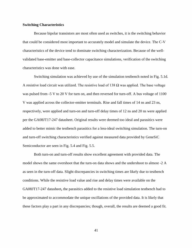
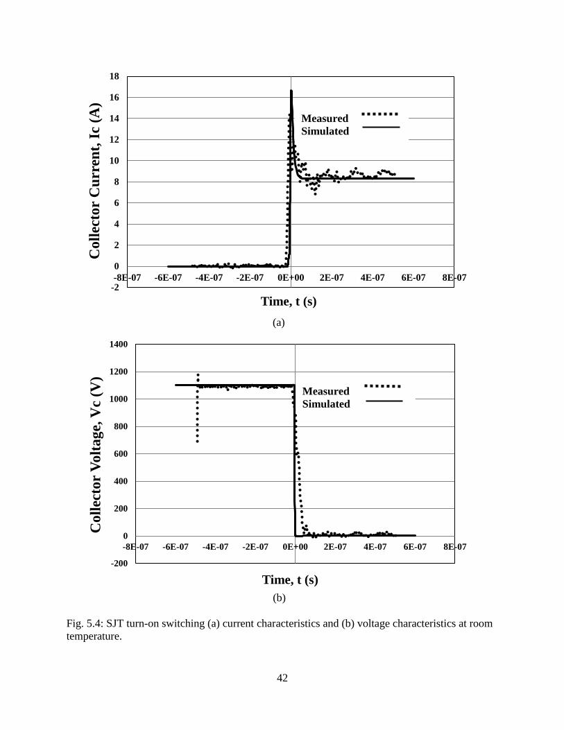
Switching Characteristics
Because bipolar transistors are most often used as switches, it is the switching behavior
that could be considered most important to accurately model and simulate the device. The C-V
characteristics of the device tend to dominate switching characterization. Because of the well-
validated base-emitter and base-collector capacitance simulations, verification of the switching
characteristics was done with ease.
Switching simulation was achieved by use of the simulation testbench noted in Fig. 5.1d.
A resistive load circuit was utilized. The resistive load of 138 Ω was applied. The base voltage
was pulsed from -5 V to 20 V for turn on, and then reversed for turn-off. A bus voltage of 1100
V was applied across the collector-emitter terminals. Rise and fall times of 14 ns and 23 ns,
respectively, were applied and turn-on and turn-off delay times of 12 ns and 20 ns were applied
per the GA08JT17-247 datasheet. Original results were deemed too ideal and parasitics were
added to better mimic the testbench parasitics for a less-ideal switching simulation. The turn-on
and turn-off switching characteristics verified against measured data provided by GeneSiC
Semiconductor are seen in Fig. 5.4 and Fig. 5.5.
Both turn-on and turn-off results show excellent agreement with provided data. The
model shows the same overshoot that the turn-on data shows and the undershoot to almost -2 A
as seen in the turn-off data. Slight discrepancies in switching times are likely due to testbench
conditions. While the resistive load value and rise and delay times were available on the
GA08JT17-247 datasheet, the parasitics added to the resistive load simulation testbench had to
be approximated to accommodate the unique oscillations of the provided data. It is likely that
these factors play a part in any discrepancies; though, overall, the results are deemed a good fit.
42
Fig. 5.4: SJT turn-on switching (a) current characteristics and (b) voltage characteristics at room
temperature.
-200
0
200
400
600
800
1000
1200
1400
-8E-07 -6E-07 -4E-07 -2E-07 0E+00 2E-07 4E-07 6E-07 8E-07
Co
llec
tor
Vo
lta
ge,
Vc
(V)
Time, t (s)
Measured
Simulated
-2
0
2
4
6
8
10
12
14
16
18
-8E-07 -6E-07 -4E-07 -2E-07 0E+00 2E-07 4E-07 6E-07 8E-07
Co
llec
tor
Cu
rren
t, I
c (A
)
Time, t (s)
Measured
Simulated
(a)
(b)
43
Fig. 5.5: SJT turn-off switching (a) current characteristics and (b) voltage characteristics at room
temperature.
-2
0
2
4
6
8
10
-8E-07 -6E-07 -4E-07 -2E-07 0E+00 2E-07 4E-07 6E-07 8E-07
Co
llec
tor
Cu
rren
t, I
c (A
)
Time, t (s)
Measured
Simulated
-200
0
200
400
600
800
1000
1200
1400
-8E-07 -6E-07 -4E-07 -2E-07 0E+00 2E-07 4E-07 6E-07 8E-07
Co
llec
tor
Vo
lta
ge,
Vc
(V)
Time, t (s)
Measured
Simulated
(a)
(b)

44
5.1.3 Temperature Scaled Results
Initial input data for simulators assumes that device measurements were taken at nominal
temperature of 25 ˚C. However, it is essential for effective modeling and circuit design for
device models to accurately predict device behavior across elevated temperatures. The device
simulations for 125 ˚C and 175 ˚C are discussed in the following sections.
Output Characteristics
Output characteristics for elevated temperatures were simulated using the same testbench
for the room temperature simulation as seen in Fig. 5.1a. TEMP was appropriately changed
within the model and model parameters were then extracted for optimal results across the risen
temperatures.
The simulated output characteristics for 125 °C were obtained by applying a base current
from 0 A to 1 A in steps of 200 mA and sweeping the collector-emitter voltage from 0 V to 8.5
V. Similarly, the simulated output characteristics for 175 °C were obtained by applying a base
current from 0 A to 1 A in steps of 200 mA and sweeping the collector-emitter voltage from 0 to
15 V. Good agreement is seen again between simulated and measured data for output
characteristics at both 125 °C and 175 °C. Overall, the verified results shown in Figs. 5.6a and
5.6b are deemed acceptable.
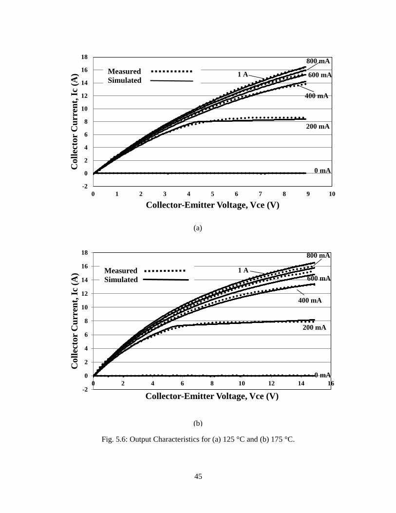
45
Fig. 5.6: Output Characteristics for (a) 125 °C and (b) 175 °C.
-2
0
2
4
6
8
10
12
14
16
18
0 1 2 3 4 5 6 7 8 9 10
Co
llec
tor
Cu
rren
t, I
c (A
)
Collector-Emitter Voltage, Vce (V)
0 mA
200 mA
400 mA
600 mA
800 mA
1 AMeasured
Simulated
-2
0
2
4
6
8
10
12
14
16
18
0 2 4 6 8 10 12 14 16
Co
llec
tor
Cu
rren
t, I
c (A
)
Collector-Emitter Voltage, Vce (V)
0 mA
200 mA
400 mA
600 mA
800 mA
1 AMeasured
Simulated
(a)
(b)
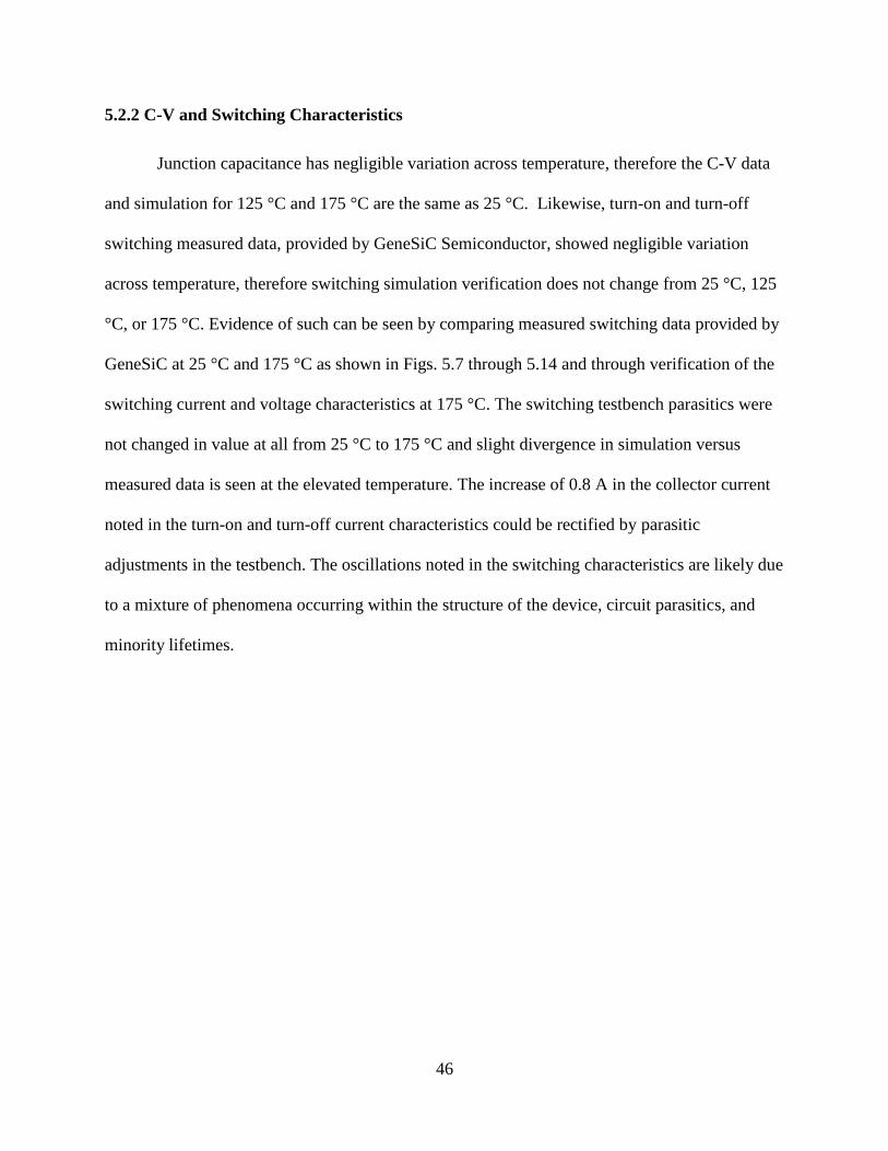
46
5.2.2 C-V and Switching Characteristics
Junction capacitance has negligible variation across temperature, therefore the C-V data
and simulation for 125 °C and 175 °C are the same as 25 °C. Likewise, turn-on and turn-off
switching measured data, provided by GeneSiC Semiconductor, showed negligible variation
across temperature, therefore switching simulation verification does not change from 25 °C, 125
°C, or 175 °C. Evidence of such can be seen by comparing measured switching data provided by
GeneSiC at 25 °C and 175 °C as shown in Figs. 5.7 through 5.14 and through verification of the
switching current and voltage characteristics at 175 °C. The switching testbench parasitics were
not changed in value at all from 25 °C to 175 °C and slight divergence in simulation versus
measured data is seen at the elevated temperature. The increase of 0.8 A in the collector current
noted in the turn-on and turn-off current characteristics could be rectified by parasitic
adjustments in the testbench. The oscillations noted in the switching characteristics are likely due
to a mixture of phenomena occurring within the structure of the device, circuit parasitics, and
minority lifetimes.
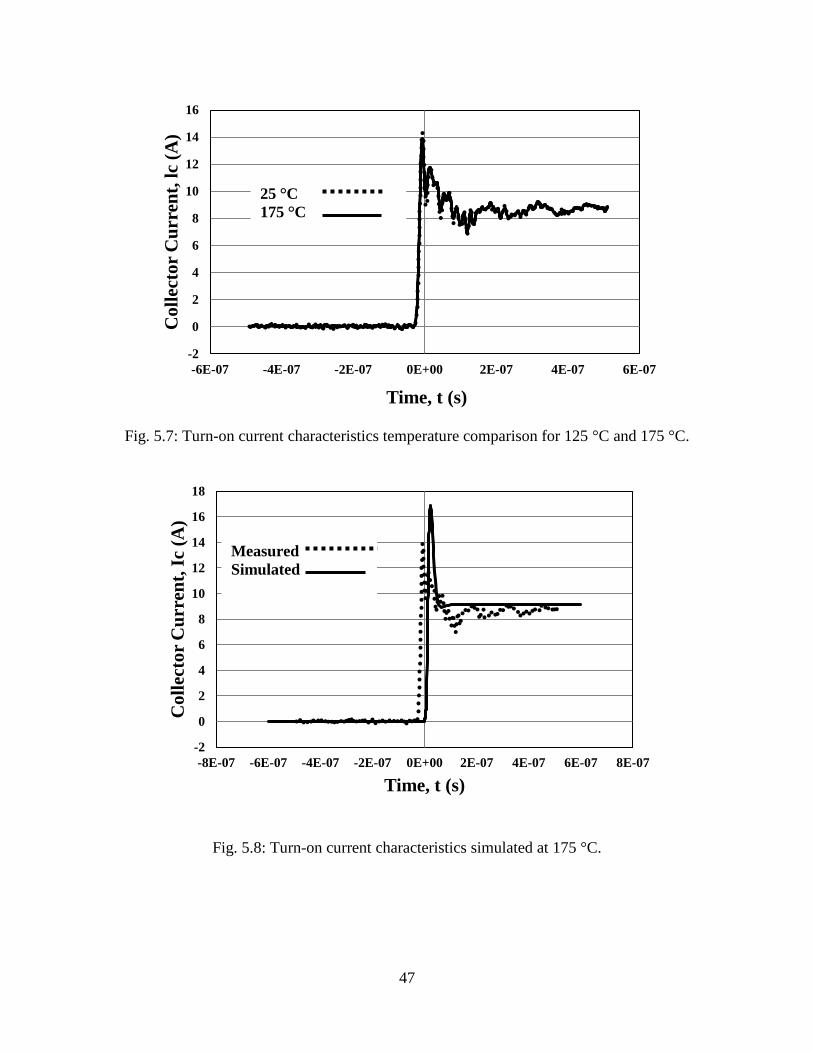
47
Fig. 5.7: Turn-on current characteristics temperature comparison for 125 °C and 175 °C.
Fig. 5.8: Turn-on current characteristics simulated at 175 °C.
-2
0
2
4
6
8
10
12
14
16
18
-8E-07 -6E-07 -4E-07 -2E-07 0E+00 2E-07 4E-07 6E-07 8E-07
Co
llec
tor
Cu
rren
t, I
c (A
)
Time, t (s)
Measured
Simulated
-2
0
2
4
6
8
10
12
14
16
-6E-07 -4E-07 -2E-07 0E+00 2E-07 4E-07 6E-07
Co
llec
tor
Cu
rren
t, l
c (A
)
Time, t (s)
25 °C
175 °C

48
Fig. 5.9: Turn-on voltage characteristics temperature comparison of 125 °C and 175 °C.
Fig. 5.10: Turn-on voltage characteristics simulated at 175 °C.
-200
0
200
400
600
800
1000
1200
1400
-6E-07 -4E-07 -2E-07 0E+00 2E-07 4E-07 6E-07
Co
llec
tor
Vo
lta
ge,
Vc
(V)
Time, t (s)
25 °C
175 °C
-200
0
200
400
600
800
1000
1200
1400
-8E-07 -6E-07 -4E-07 -2E-07 0E+00 2E-07 4E-07 6E-07 8E-07
Co
llec
tor
Vo
lta
ge,
Vc
(V)
Time, t (s)
Measured
Simulated
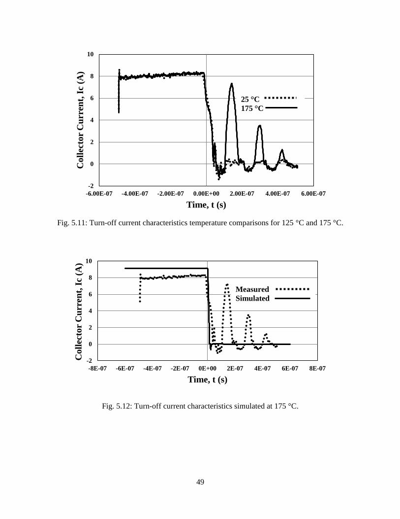
49
Fig. 5.11: Turn-off current characteristics temperature comparisons for 125 °C and 175 °C.
Fig. 5.12: Turn-off current characteristics simulated at 175 °C.
-2
0
2
4
6
8
10
-6.00E-07 -4.00E-07 -2.00E-07 0.00E+00 2.00E-07 4.00E-07 6.00E-07
Co
llec
tor
Cu
rren
t, I
c (A
)
Time, t (s)
25 °C
175 °C
-2
0
2
4
6
8
10
-8E-07 -6E-07 -4E-07 -2E-07 0E+00 2E-07 4E-07 6E-07 8E-07
Co
llec
tor
Cu
rren
t, I
c (A
)
Time, t (s)
Measured
Simulated

50
Fig. 5.13: Turn-off voltage characteristics comparison for 125 °C and 175 °C.
Fig. 5.14: Turn-off voltage characteristics simulated at 175 °C.
0
200
400
600
800
1000
1200
1400
-6E-07 -4E-07 -2E-07 0E+00 2E-07 4E-07 6E-07
Co
llec
tor
Vo
lta
ge,
Vc
(V)
Time, t (s)
25 °C
175 °C
-200
0
200
400
600
800
1000
1200
1400
-8E-07 -6E-07 -4E-07 -2E-07 0E+00 2E-07 4E-07 6E-07 8E-07
Co
llec
tor
Vo
lta
ge,
Vc
(V)
Time, t (s)
Measured
Simulated

51
CHAPTER 6: SUMMARY AND CONCLUSIONS
The work presented in this thesis aimed to develop the first temperature-scaled compact
model for use of a 1.7 kV, 8 A GeneSic SiC SJT. The benefits of SiC as a device material were
discussed by describing the material and electrical advantages over its Si counterpart. A model
was developed using a GP based model represented in [23] and with a Verilog-A implementation
derived from the Berkeley Spice3f5 implementation. The model was then validated and verified
in IC-CAP and Paragon2 for the output, C-V, and switching characteristics.
SiC SJTs offer the ability to reduce the size and increase efficiency of power electronics
applications. Use in micro-grids, electric vehicles, solar inverters and many more applications
will be innovated by use of SJTs operating at high voltages, frequencies, and temperatures with
low on-resistances. These SJTs aim to be competitors to SiC MOSFETS. GeneSiC has optimally
designed these devices with characteristics similar to those of SiC MOSFETs including fast
switching capabilities, a square reverse-biased safe operating area, as well as temperature-
independent transient energy losses and switching times. A main distinguishing factor of these
devices is that they are capable of being driven by commercially available gate drivers, unlike
other SiC switches.
With advances in SiC technology and the rise of newly engineered bipolar transistors as
MOSFET competitors, having accurate compact models is a tremendous asset. This work
successfully laid a solid foundation for modeling and simulation of GeneSiC’s line of SiC
Junction Transistors.
Future Work
Though this work has laid a solid foundation for modeling of GeneSiC’s SJTs, further
work could be done to improve model performance for this and other bipolar transistors. The

52
results from the model compared to real world data were effective at capturing the ideal
transistor characteristics. However, for added efficiency and accuracy, the base of the model
could be converted from the SGP model to a more advanced bipolar model. The Mextram model
would serve as a reasonable alternative to the SGP model once modified for super-junction
applications.

53
REFERENCES
[1] C. M. Snowden, “Semiconductor device modelling,” Reports Prog. Phys., vol. 48, no. 2, p.
223, 1985.
[2] W. Peter and H. A. Mantooth, Model-Based Engineering for Complex Electronic Systems.
Elsevier, 2013.
[3] E. Santi, J. L. Hudgins, and H. A. Mantooth, “Variable Model Levels for Power
Semiconductor Devices,” Proc. 2007 Summer Comput. Simul. Conf. Scsc, pp. 276–283,
2007.
[4] R. Singh, S. Sundaresan, E. Lieser, and M. Digangi, “1200 V SiC ‘Super’ Junction
Transistors operating at 250° C with extremely low energy losses for power conversion
applications,” in Applied Power Electronics Conference and Exposition (APEC), 2012
Twenty-Seventh Annual IEEE, 2012, pp. 2516–2520.
[5] R. Singh, S. Sundaresan, E. Lieser, and M. Digangi, “1200 V SiC ‘Super’ Junction
Transistors operating at 250° C with extremely low energy losses for power conversion
applications,” in Applied Power Electronics Conference and Exposition (APEC), 2012
Twenty-Seventh Annual IEEE, 2012, pp. 2516–2520.
[6] S. Sundaresan, R. Singh, and R. W. Jochnson, Silicon Carbide Super Junction Transistors
Operations at 500 C. .
[7] S. G. Sundaresan, A.-M. Soe, and R. Singh, “Stability of Electrical Characteristics of SiC
‘Super’ Junction Transistors under Long-Term DC and Pulsed Operation at various
Temperatures,” Mrs Proc., vol. 1433, Jan. 2012.
[8] S. Sundaresan, S. Jeliazkov, B. Grummel, and R. Singh, “10 kV SiC BJTs—Static,
switching and reliability characteristics,” in Power Semiconductor Devices and ICs
(ISPSD), 2013 25th International Symposium on, 2013, pp. 303–306.
[9] T. Fujihira, “Theory of Semiconductor Superjunction Devices,” Jpn. J. Appl. Phys., vol. 36,
pp. 6254–6262, Oct. 1997.
[10] T. Fujihira and Miyasaka, Yasushi, “SJ MOSFET,” in Proceedings of 1998 International
Symposium on Power Semiconductor Devices & ICs, Kyoto, pp. 423–426.
[11] Y. Oonishi, A. Ooi, and T. Shimatou, “Superjunction MOSFET,” Power Semicond.
Contrib. Energy Environ. Reg., vol. 56, no. 2, p. 65, 2010.
54
[12] T. Henson and J. Cao, “Low voltage super junction MOSFET simulation and
experimentation,” in Power Semiconductor Devices and ICs, 2003. Proceedings. ISPSD’03.
2003 IEEE 15th International Symposium on, 2003, pp. 37–40.
[13] X.-B. Chen and J. K. Sin, “Optimization of the specific on-resistance of the COOLMOS
TM,” Electron Devices Ieee Trans., vol. 48, no. 2, pp. 344–348, 2001.
[14] L. S. Ramsdell, “Studies on Silicon Carbide,” Am. Miner., vol. 32, no. 1–2, pp. 64–82, Feb.
1947.
[15] B. J. Baliga, Fundamentals of power semiconductor devices. Springer Science & Business
Media, 2010.
[16] Sima Dimitrijev, Principles of Semiconductor Devices, Second Edition. Oxford University
Press, 2011.
[17] G. Massobrio and Paolo Antognetti, Semiconductor Device Modeling with SPICE, Second
Edition. Mc Graw-Hill Education, 1998.
[18] Getreu, Ian, Modeling the Bipolar Transistor, 2009th ed. Ian Getreu, 2009.
[19] N. Mohan, W. P. Robbins, and T. M. Undeland, Power Electronics Converters,
Applications and Design, 3rd ed. John Wiley & Sons Inc., 2002.
[20] J. J. Ebers and J. L. Moll, “Large-signal behavior of junction transistors,” Proc. Ire, vol. 42,
no. 12, pp. 1761–1772, 1954.
[21] H.K. Gummel and H.C. Poon, “An integral charge-control model of bipolar transistors,”
Bell Syst. Tech. J., vol. 49, pp. 827–852, 1970.
[22] G. M. Kull, L. W. Nagel, S.-W. Lee, P. Lloyd, E. J. Prendergast, and H. Dirks, “A unified
circuit model for bipolar transistors including quasi-saturation effects,” Electron Devices
IEEE Trans., vol. 32, no. 6, pp. 1103–1113, 1985.
[23] H. Jeong and J. Fossum, “A charge-based large signal bipolar transistor model for device
and circuit simulation,” IEEE Trans. Electron. Devices, vol. 36, no. 1, pp. 124–131, 1987.
[24] C. Xu and D. Schroeder, “A Power Bipolar Junction Transistor Model describing Static and
Dynamic Behaviour,” IEEE Trans Power Electron., vol. 7, no. 4, pp. 734–740, 1992.
[25] J. Berkner, “Compact Models for Bipolar Transistors,” Eur. Ic-Cap Device Model. Work.,
2002.
55
[26] A. Chakravorty, R. Garg, and C. K. Maiti, “Comparison of state-of-the-art bipolar compact
models for SiGe-HBTs,” Appl. Surf. Sci., vol. 224, no. 1–4, pp. 354–360, Mar. 2004.
[27] F. Sischka, “The VBIC Model.”
https://efabless.atlassian.net/wiki/download/.../The%20VBIC%20Model.pdf?api=v 2002.
[28] GeneSiC Semiconductor, www.genesicsemi.com
[29] Y. Huang, S. Cheng, W. Zhou, and K. Sheng, “Modeling of a 1200 V 6 A SiC bipolar
junction transistor,” in Energy Conversion Congress and Exposition (ECCE), 2013 IEEE,
2013, pp. 934–939.
56
APPENDIX A: DESCRIPTION OF RESEARCH FOR POPULAR PUBLICATION
Transistors are electronic devices generally used to perform as switches in electronic
circuits. GeneSiC Semiconductor has, in recent years, developed and released a 1700 V class of
silicon-carbide (SiC) “Super” Junction Transistors (SJTs). GeneSiC Semiconductors aims to
increase power conversion efficiency and reduce the size, weight, volume of commercial power
electronics through incorporation of these SiC SJTs.
SiC SJTs offer the ability to reduce the size and increase efficiency of power electronics
applications. Use in micro-grids, electric vehicles, solar inverters and many more applications
will be innovated by use of SJTs operating at high voltages, frequencies, and temperatures while
maintaining low on-resistances.
The first-ever 1.7 kV, 8 A SiC physics-based circuit model is developed for behavior
prediction, modeling and simulation of the GeneSiC “Super” Junction Transistor. The model is
designed to predict and simulate the SJT behavior under performance conditions defined by the
user. Model accuracy is paramount in successfully describing the device behavior.
Transistor modeling and simulation for device performance is not a new concept.
Therefore, an already-existing model served as a base for this work. The Gummel-Poon
transistor model was used and a modified quasi-saturation model was added to accurately
describe the SJT behavior.
The model provided accurate and acceptable simulations of the GeneSiC 1.7 kV 8 A SJT.
With advances in SiC technology and the rise of newly engineered bipolar transistors, having
accurate compact models is a tremendous asset leading to improved manufacturing efficiency
and productivity.

57
APPENDIX B: EXECUTIVE SUMMARY OF NEWLY CREATED INTELLECTUAL
PROPERTY
There is no newly created intellectual property within this work.

58
APPENDIX C: POTENTIAL PATENT AND COMMERCIALIZATION ASPECTS OF
LISTED INTELLECTUAL PROPERTY ITEMS
No potential patents or commercialization opportunities were created with this work.

59
APPENDIX D: BROADER IMPACT OF RESEARCH
D.1 Applicability of Research Methods to Other Problems
SiC is deemed advantageous for use in power electronics applications. SiC provides a
wide band gap, high critical electric field, and high thermal conductivity in comparison to Si,
providing opportune circumstance for improved and more efficient power device performance.
SiC BJTs provide more stable operation across a wider temperature range than Si counterparts.
Providing accurate device models maintains pivotal in circuit design and electrical
efficiency. By producing well-developed models, SiC devices are able to be utilized in circuits
that improve and impact overall electricity consumption worldwide.
D.2 Impact of Research Results on U.S. and Global Society
Bipolar transistors are the device of choice for many analog circuits and in discrete circuit
design. SJTs increase conversion efficiency and reduce the size, weight, and volume of power
electronics. Higher switching frequencies these devices are able to achieve allow for cost savings
on a systems level as well, which impacts the economy. These devices affect a plethora of
applications including DC micro-grids, telecom and networking power supplies, and industrial
motor control systems.
D.3 Impact of Research Results on Environment
The availability of fully-functioning and accurate device models allows for efficiency-
sustaining manufacturing. Solar inverters, wind power systems, and electric vehicles, and other
measures of renewable energy applications benefit from these devices and their models.

60
APPENDIX E: MICROSOFT PROJECT FOR MS MICROEP DEGREE
60

61
Appendix F: IDENTIFICATION OF ALL SOFTWARE USED IN RESEARCH AND
THESIS GENERATION
Computer #1:
Model Number: Dell Optiplex 980
Serial Number: HJNDPP1
Location: CSRCW47
Owner: Dr. Alan Mantooth
Software #1:
Name: Paragon2
Created by: University of Arkansas
Software #2:
Name: IC-CAP
Purchased by: Dr. H. Alan Mantooth
Software #3:
Name: Adobe Acrobat Professional 10.0
Purchased by: University of Arkansas Site License
Software #4:
Name: Microsoft Office 2010
Purchased by: University of Arkansas Site License
Computer #2:
Model Number: Acer Aspire Z3-605 Windows 10 Home Version 1511
Serial Number: 00326-10000-00000-AA625
Location: Personal residence
Owner: Brooks
Software #5
Name: Microsoft Office 2010
Purchased by: Brooks
Computer #3
Software #6
Name: Microsoft Office 2010
Purchased by: Brooks