modeling and characterization of substrate resistance for ... · modeling and characterization of...
TRANSCRIPT
MODELING AND CHARACTERIZATION OF SUBSTRATE RESISTANCE
FOR DEEP SUBMICRON ESD PROTECTION DEVICES
A DISSERTATIONSUBMITTED TO THE DEPARTMENT OF ELECTRICAL ENGINEERING
AND THE COMMITTEE ON GRADUATE STUDIESOF STANFORD UNIVERSITY
IN PARTIAL FULFILLMENT OF THE REQUIREMENTSFOR THE DEGREE OF
DOCTOR OF PHILOSOPHY
XIN YI ZHANGAUGUST 2002
C Copyright by Xin Yi Zhang 2002All rights Reserved
ii
ABSTRACT
As device dimensions continue to shrink, higher current densities and lower voltage
tolerances make ESD, or Electrostatic Discharge, an increasingly important issue to
guard against for ensuring reliability. Industry data show that one-third of all customer
returns are due to ESD.
IC chips are protected against ESD by on-chip protection circuits, which are
connected between the I/O pads and the internal circuitry. The protection circuit, which
consists of protection devices, is designed to rapidly discharge high current in an ESD
event.
Typically, the design of ESD protection circuits is an empirical approach. Several
candidate circuits are fabricated, characterized, and evaluated for key physical and
performance parameters using known testing techniques. Different combinations of
device geometries and process technologies are evaluated until a suitable circuit with the
desired characteristics is found. This resource intensive design approach clearly
motivates a simulation based solution which enables quicker turnaround as well as
obvious cost-savings in materials and resources.
iv
The focus of our research is on modeling and characterizing ESD protection
devices, especially the substrate resistance, in a state-of-art CMOS technology. Unlike
normal MOS operation, both the channel and the substrate region in a given device need
to be modeled to show that current extends from the channel into the substrate under ESD
stress. We begin by developing a circuit model to simulate the high current characteristics
under ESD stress since none exist in commercial circuit simulators. We then demonstrate
the extraction of circuit-level parameters from experimental data using a systematic
extraction methodology.
The next phase of our research extends the circuit model to enable simulation of
different layout and process variations by focusing on modeling substrate resistance.
Substrate resistance determines the on/off state of the protection device by providing
current discharge paths from drain to substrate and drain to source. This parameter also
captures the substrate interactions of different protection circuit elements.
In order to address the sensitivity of substrate resistance to layout and process varia-
tions, we propose a new methodology called quasi-mixed-mode (QMM) device and cir-
cuit simulation approach, and we will describe the QMM approach in detail as well as
illustrate the application of the model to the modeling of substrate resistance for deep sub-
micron ESD protection nMOSFETs. The substrate resistance simulated by this method
shows good agreement with the values extracted from experimental data. This technique
can be employed to simulate turn-on characteristics of ESD protection devices and deter-
mine the impact of process and layout variations on their reliability before fabrication of
the actual devices.
v
ACKNOWLEDGMENTS
I would not have finished this thesis without the help and encouragement from a
number of individuals. First, I would like to thank my advisor, Professor Robert Dutton.
He introduced me to the subject of ESD circuit and device modeling. He steered me
towards the idea to use numerical simulation to solve layout dependent ESD modeling
problems. I learnt to treasure the free and cooperative work environment that Bob fosters
among his students.
I also had the good fortune of working with people who are leaders in the field of
ESD device design, modeling, and characterization. Drs. Julian Chen and Tom Vrotsos
offered me a summer job at Texas Instruments, giving me an opportunity to study the ESD
problem at the industry level. While there at TI, I was lucky to have met Dr. Ajith Amer-
askera, Dr. Charvaka Duvvury, Dr. Shridar Ramaswamy, and Gupta Vikas. They, espe-
cially Ajith, have helped me tremendously with my research by letting me take
measurements of their test structures and helping me to analyze the resulting data.
Dr. Stephen Beebe, who was also Bob’s student and also did his dissertation on ESD
modeling, directed me into ESD work at Advanced Micro Devices. While at AMD, I
learned how to effectively apply device simulation to analyze ESD problems.
Dr. Tim Maloney from Intel also gave me valuable feedbacks on my research.
vi

I wrote more than half of my thesis while working full time at Marvell Semiconduc-
tor Technology. This exciting job provided me with important insights into the interactions
between the protection and protected elements. I want to thank Dr. Joe Li for all the help-
ful discussions and ideas on ESD protection. I also want to thank Drs. Eric Minami and
Leechung Yiu for all their support and encouragement.
Of course, none of this would have been possible without the generous financial sup-
port from Semiconductor Research Corporation. I am very grateful to SRC for giving me
this great opportunity to carry out my research.
My years at Stanford has been wonderful. Special thanks go to Dr. Zhiping Yu, not
only for his many lectures on device physics but also for his advice on life in general.
Kaustav Banerjee, who is my co-author, helped me a lot by going over my results and
proof-reading my paper. I would also like to thank my orals and reading committee: Drs.
Robert Dutton, Bruce Wooley, Kenneth Goodson, Zhiping Yu, and Kunle Olukotun. In
addition, I want to thank the whole TCAD group, specifically my officemates Edward,
Francis, Zak, Choshu, Jaejung, Ken, Tao, Nathan, and Michael for all the discussions and
support over the years. Without Dan Yergeau answering and solving all my Unix questions
and problems, I would be still working on my thesis. Fely, Miho, and Maria also made my
life easier by providing all the administrative support, especially for Fely’s friendship and
guidance on navigating through all the deadlines during my graduate career.
Last but certainly not the least, I would like to thank all my friends who made my
bad days bearable and good days wonderful at Stanford, especially Marianna Landa for
tirelessly proof-reading my thesis, polishing all the rough sentences, and Jeff for his ever-
lasting support and encouragement, and of course Mom, Dad, and Frankie who have
always encouraged me during these many years of study.
This thesis is dedicated to my grandparents.
vii

CONTENTS
Abstract iv
Acknowledgments vi
List of Tables xi
List of Figures xii
1 Introduction 1
1.1 ESD and ESD Protection in the Semiconductor Industry . . . . . . . . . . . . 1
1.2 The Importance of Modeling ESD Protection Circuits and Devices. . . . 4
1.3 Previous Studies of the ESD Model and Existing Simulation Tools . . . . 7
1.4 Outline . . . . . . . . . . . . . . . . . . . . . . . . . . . . . . . . . . . . . . . . . . . . . . . . . . . 9
2 ESD Device Characterization and Compact Model 11
2.1 Types of ESD Stress. . . . . . . . . . . . . . . . . . . . . . . . . . . . . . . . . . . . . . . . 11
2.2 Device Operation . . . . . . . . . . . . . . . . . . . . . . . . . . . . . . . . . . . . . . . . . . 15
2.3 Compact Model for Transistors . . . . . . . . . . . . . . . . . . . . . . . . . . . . . . . 19
2.4 Modeling of Igen and M . . . . . . . . . . . . . . . . . . . . . . . . . . . . . . . . . . . . . 23
viii
2.5 Extraction Methodology for M parameters . . . . . . . . . . . . . . . . . . . . . . 27
2.6 Substrate Resistance Model . . . . . . . . . . . . . . . . . . . . . . . . . . . . . . . . . . 36
2.7 Extraction of Rsub Parameters . . . . . . . . . . . . . . . . . . . . . . . . . . . . . . . 44
2.8 Parasitic Bipolar Transistor Modeling . . . . . . . . . . . . . . . . . . . . . . . . . . 46
2.9 Extraction of β . . . . . . . . . . . . . . . . . . . . . . . . . . . . . . . . . . . . . . . . . . . . 49
2.10 High Current ESD Compact Model Implementation . . . . . . . . . . . . . . 51
2.11 Impacts of Scaling . . . . . . . . . . . . . . . . . . . . . . . . . . . . . . . . . . . . . . . . . 55
3 The Substrate Resistance Model: The Quasi-Mixed-ModeMethodology 60
3.1 Rsub Model Background . . . . . . . . . . . . . . . . . . . . . . . . . . . . . . . . . . . . 60
3.2 The QMM Approach . . . . . . . . . . . . . . . . . . . . . . . . . . . . . . . . . . . . . . . 65
3.3 Verification of Simplified Device Simulation . . . . . . . . . . . . . . . . . . . . 71
3.4 QMM Method vs. Full Device Simulation . . . . . . . . . . . . . . . . . . . . . . 77
3.5 Discussion of the QMM Approach . . . . . . . . . . . . . . . . . . . . . . . . . . . . 87
4 Calibration and Simulation of Substrate Resistance Using the QMM Methodology 89
4.1 Calibration and Simulation of Substrate Resistance for SingleFinger Devices . . . . . . . . . . . . . . . . . . . . . . . . . . . . . . . . . . . . . . . . . . . . 89
4.2 Effects of Layout and Process . . . . . . . . . . . . . . . . . . . . . . . . . . . . . . . . 92
4.3 Motivation for 3D substrate Resistance Model . . . . . . . . . . . . . . . . . . 103
4.4 Pseudo 3D Substrate Resistance Model. . . . . . . . . . . . . . . . . . . . . . . . 105
4.5 Substrate Resistance Model for Multi-Finger ProtectionDevices. . . . . . . . . . . . . . . . . . . . . . . . . . . . . . . . . . . . . . . . . . . . . . . . . 113
ix

5. Conclusions and Future Work 124
5.1 Contributions . . . . . . . . . . . . . . . . . . . . . . . . . . . . . . . . . . . . . . . . . . . . 124
5.2 Suggested Future Work . . . . . . . . . . . . . . . . . . . . . . . . . . . . . . . . . . . . 128
Bibliography 130
x

LIST OF TABLES
Table 2-1 M Parameter’s Value. . . . . . . . . . . . . . . . . . . . . . . . . . . . . . . . . . . . . . . . . . . . 35
Table 2-2 Rsub and BJT Parameters . . . . . . . . . . . . . . . . . . . . . . . . . . . . . . . . . . . . . . . . 51
Table 3-1 Comparison of Simulation Speed . . . . . . . . . . . . . . . . . . . . . . . . . . . . . . . . . . 88
Table 4-1 Device A-L . . . . . . . . . . . . . . . . . . . . . . . . . . . . . . . . . . . . . . . . . . . . . . . . . . . 91
xi
LIST OF FIGURES
Figure 1-1 Block diagram of input and output protection circuits . . . . . . . . . . . . . . . . . 2
Figure 1-2 An input protection circuit . . . . . . . . . . . . . . . . . . . . . . . . . . . . . . . . . . . . . . . 3
Figure 2-1 Lumped circuit diagram. . . . . . . . . . . . . . . . . . . . . . . . . . . . . . . . . . . . . . . . 13
Figure 2-2 HPSICE generated HBM waveform . . . . . . . . . . . . . . . . . . . . . . . . . . . . . . 14
Figure 2-3 HP4145 Parameter Analyzer . . . . . . . . . . . . . . . . . . . . . . . . . . . . . . . . . . . . 18
Figure 2-4 Two-dimensional cross section of a nMOS . . . . . . . . . . . . . . . . . . . . . . . . . 20
Figure 2-5 The compact model . . . . . . . . . . . . . . . . . . . . . . . . . . . . . . . . . . . . . . . . . . . 22
Figure 2-6 Extraction process of Vdch . . . . . . . . . . . . . . . . . . . . . . . . . . . . . . . . . . . . . . 30
Figure 2-7 The extracted Vdchs . . . . . . . . . . . . . . . . . . . . . . . . . . . . . . . . . . . . . . . . . . . 31
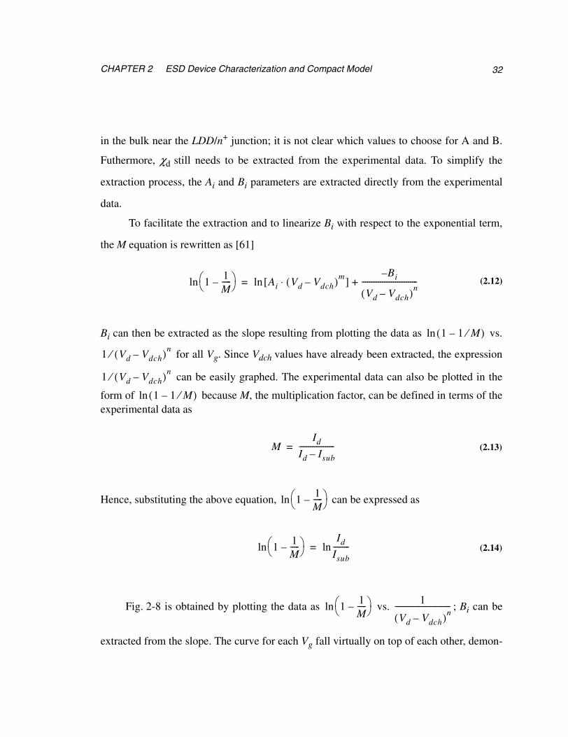
Figure 2-8 Data points . . . . . . . . . . . . . . . . . . . . . . . . . . . . . . . . . . . . . . . . . . . . . . . . . . 34
Figure 2-9 Comparison between calculated M and experimental M. . . . . . . . . . . . . . . 35
Figure 2-10 m=0.35 and n=1 . . . . . . . . . . . . . . . . . . . . . . . . . . . . . . . . . . . . . . . . . . . . . . 36
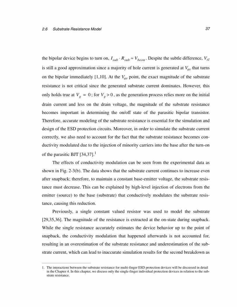
Figure 2-11 ESD I-V curve . . . . . . . . . . . . . . . . . . . . . . . . . . . . . . . . . . . . . . . . . . . . . . . 39
Figure 2-12 Dynamic substrate resistance. . . . . . . . . . . . . . . . . . . . . . . . . . . . . . . . . . . . 40
Figure 2-13 Plot on silicided device . . . . . . . . . . . . . . . . . . . . . . . . . . . . . . . . . . . . . . . . 41
Figure 2-14 Reduction of Vsb to Vsb’ . . . . . . . . . . . . . . . . . . . . . . . . . . . . . . . . . . . . . . . 43
Figure 2-15 Straight line . . . . . . . . . . . . . . . . . . . . . . . . . . . . . . . . . . . . . . . . . . . . . . . . . 45
xii
Figure 2-16 Two solid lines . . . . . . . . . . . . . . . . . . . . . . . . . . . . . . . . . . . . . . . . . . . . . . . 53
Figure 2-17 Simulated ESD I-V curve . . . . . . . . . . . . . . . . . . . . . . . . . . . . . . . . . . . . . . 54
Figure 2-18 Simulated Isub vs. Id . . . . . . . . . . . . . . . . . . . . . . . . . . . . . . . . . . . . . . . . . . . 55
Figure 2-19 Junction breakdown voltage . . . . . . . . . . . . . . . . . . . . . . . . . . . . . . . . . . . . 57
Figure 2-20 Y-axis intercept . . . . . . . . . . . . . . . . . . . . . . . . . . . . . . . . . . . . . . . . . . . . . . 58
Figure 3-1 ESD I-V curve . . . . . . . . . . . . . . . . . . . . . . . . . . . . . . . . . . . . . . . . . . . . . . . 63
Figure 3-2 The QMM approach. . . . . . . . . . . . . . . . . . . . . . . . . . . . . . . . . . . . . . . . . . . 66
Figure 3-3 The flow diagram. . . . . . . . . . . . . . . . . . . . . . . . . . . . . . . . . . . . . . . . . . . . . 68
Figure 3-4 Circuit-level Schematic . . . . . . . . . . . . . . . . . . . . . . . . . . . . . . . . . . . . . . . . 69
Figure 3-5 Boundary condition . . . . . . . . . . . . . . . . . . . . . . . . . . . . . . . . . . . . . . . . . . . 70
Figure 3-6 The electric field . . . . . . . . . . . . . . . . . . . . . . . . . . . . . . . . . . . . . . . . . . . . . 72
Figure 3-7 The electric field and electron/hole concentration. . . . . . . . . . . . . . . . . . . . 73
Figure 3-8 The E// contours . . . . . . . . . . . . . . . . . . . . . . . . . . . . . . . . . . . . . . . . . . . . . . 75
Figure 3-9 The generation area . . . . . . . . . . . . . . . . . . . . . . . . . . . . . . . . . . . . . . . . . . . 76
Figure 3-10 The artificially injected peak electron concentration. . . . . . . . . . . . . . . . . . 78
Figure 3-11 A two-dimensional cross section . . . . . . . . . . . . . . . . . . . . . . . . . . . . . . . . . 79
Figure 3-12 The Isub vs. Id curves . . . . . . . . . . . . . . . . . . . . . . . . . . . . . . . . . . . . . . . . . . 80
Figure 3-13 The β vs. Ic curves . . . . . . . . . . . . . . . . . . . . . . . . . . . . . . . . . . . . . . . . . . . . 82
Figure 3-14 Id vs. Vd plots. . . . . . . . . . . . . . . . . . . . . . . . . . . . . . . . . . . . . . . . . . . . . . . . 84
Figure 3-15 Comparison of Isub vs. Id curves . . . . . . . . . . . . . . . . . . . . . . . . . . . . . . . . . 85
Figure 3-16 Rsub0s . . . . . . . . . . . . . . . . . . . . . . . . . . . . . . . . . . . . . . . . . . . . . . . . . . . . . . 86
Figure 4-1 Two different types of layouts . . . . . . . . . . . . . . . . . . . . . . . . . . . . . . . . . . . 90
Figure 4-2 The LDD and S/D junction depth . . . . . . . . . . . . . . . . . . . . . . . . . . . . . . . . 92
Figure 4-3 Experimental Isub vs. Id curves . . . . . . . . . . . . . . . . . . . . . . . . . . . . . . . . . . 93
Figure 4-4 The resistance values . . . . . . . . . . . . . . . . . . . . . . . . . . . . . . . . . . . . . . . . . . 94
xiii

Figure 4-5 Experimental Isub vs. Id curves for Device C. . . . . . . . . . . . . . . . . . . . . . . . 95
Figure 4-6 The resistance values for Process X . . . . . . . . . . . . . . . . . . . . . . . . . . . . . . 96
Figure 4-7 The resistance values for Process Y . . . . . . . . . . . . . . . . . . . . . . . . . . . . . . 97
Figure 4-8 The current flowlines . . . . . . . . . . . . . . . . . . . . . . . . . . . . . . . . . . . . . . . . . . 98
Figure 4-9 Rsub0 values between 1-10µm Lpns . . . . . . . . . . . . . . . . . . . . . . . . . . . . . . . 99
Figure 4-10 β for devices C and F . . . . . . . . . . . . . . . . . . . . . . . . . . . . . . . . . . . . . . . . . 101
Figure 4-11 The ESD I-V curve of device F . . . . . . . . . . . . . . . . . . . . . . . . . . . . . . . . . 106
Figure 4-12 Device 1 . . . . . . . . . . . . . . . . . . . . . . . . . . . . . . . . . . . . . . . . . . . . . . . . . . . 107
Figure 4-13 Plot from the device with p+ guard ring . . . . . . . . . . . . . . . . . . . . . . . . . . 109
Figure 4-14 The flow diagram. . . . . . . . . . . . . . . . . . . . . . . . . . . . . . . . . . . . . . . . . . . . 110
Figure 4-15 The true 3D representation of the device. . . . . . . . . . . . . . . . . . . . . . . . . . 114
Figure 4-16 Rsub0, 3Dr and Rsub0, 3Dr . . . . . . . . . . . . . . . . . . . . . . . . . . . . . . . . . . . . . . 116
Figure 4-17 A six-fingered nMOS. . . . . . . . . . . . . . . . . . . . . . . . . . . . . . . . . . . . . . . . . 117
Figure 4-18 The cross-section of the multi-fingered device . . . . . . . . . . . . . . . . . . . . . 118
Figure 4-19 The substrate resistance for each finger. . . . . . . . . . . . . . . . . . . . . . . . . . . 120
Figure 4-20 The final substrate resistance per each finger . . . . . . . . . . . . . . . . . . . . . . 121
Figure 4-21 Three fingers out of six fingers . . . . . . . . . . . . . . . . . . . . . . . . . . . . . . . . . 122
xiv

CHAPTER 1
INTRODUCTION
1.1 ESD AND ESD PROTECTION IN THE SEMICONDUCTOR
INDUSTRY
A commonly observed phenomenon, Electrostatic Discharge (ESD) involves a rapid
discharge of previously accumulated static electricity [1,2]. ESD takes place both when
we get “zapped”, reaching for the doorknob after walking across a carpet or when light-
ning strikes and causes damage or even fires. The two ESD events differ greatly in terms
of the magnitude and duration of discharge, and the resulting damage. If the same tiny
amount of static energy from the carpet walk discharges into a much smaller area of an
integrated circuit (IC) when we touch an IC chip, the resulting damage to the IC can be
equivalent to that of a lightning strike. The seemingly small energy discharge resulting
1
CHAPTER 1 Introduction 2
from touching, rubbing, and sliding the chip during the IC manufacturing process can
greatly damage the circuitry [1,3].
In fact, ESD occurring at the chip level is one of the major causes for IC failure in
the semiconductor industry. Industry data show that roughly one-third of all product
returns and greater than 10% of all IC failures are due to the ESD damage [1,3-8]. As the
feature sizes continue to shrink with each new generation of technology, higher current
densities and lower voltage tolerances will only exacerbate this already critical problem.
We are facing an increased need for more robust on-chip circuits to protect the ICs against
ESD. Connected between the I/O pads and the internal circuitry, and composed of the pro-
tection devices, combinations of devices and circuits are designed to rapidly discharge the
high current in the event of ESD [2,9-10].
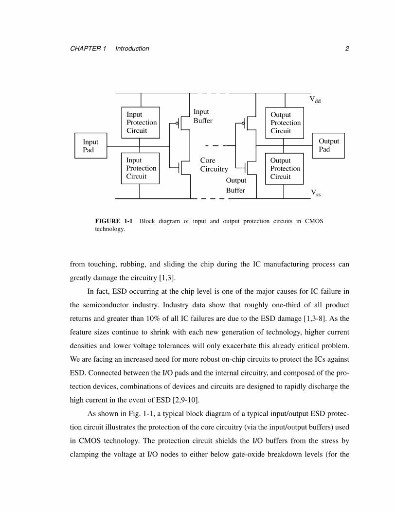
As shown in Fig. 1-1, a typical block diagram of a typical input/output ESD protec-
tion circuit illustrates the protection of the core circuitry (via the input/output buffers) used
in CMOS technology. The protection circuit shields the I/O buffers from the stress by
clamping the voltage at I/O nodes to either below gate-oxide breakdown levels (for the
InputPad
OutputPad
InputProtectionCircuit
InputProtectionCircuit
OutputProtectionCircuit
OutputProtectionCircuit
Vdd
Vss
FIGURE 1-1 Block diagram of input and output protection circuits in CMOStechnology.
InputBuffer
OutputBuffer
CoreCircuitry
31.1 Esd and Esd Protection In the Semiconductor Industry
input gates) or below drain-substrate junction breakdown levels (for the output buffers).
At the same time, the protection circuit effectively shunts the ESD current either to Vss or
Vdd without going through internal circuitry. Devices like diodes, resistors, and transistors
can all be used as efficient voltage clamps for input protection circuits [1-4].
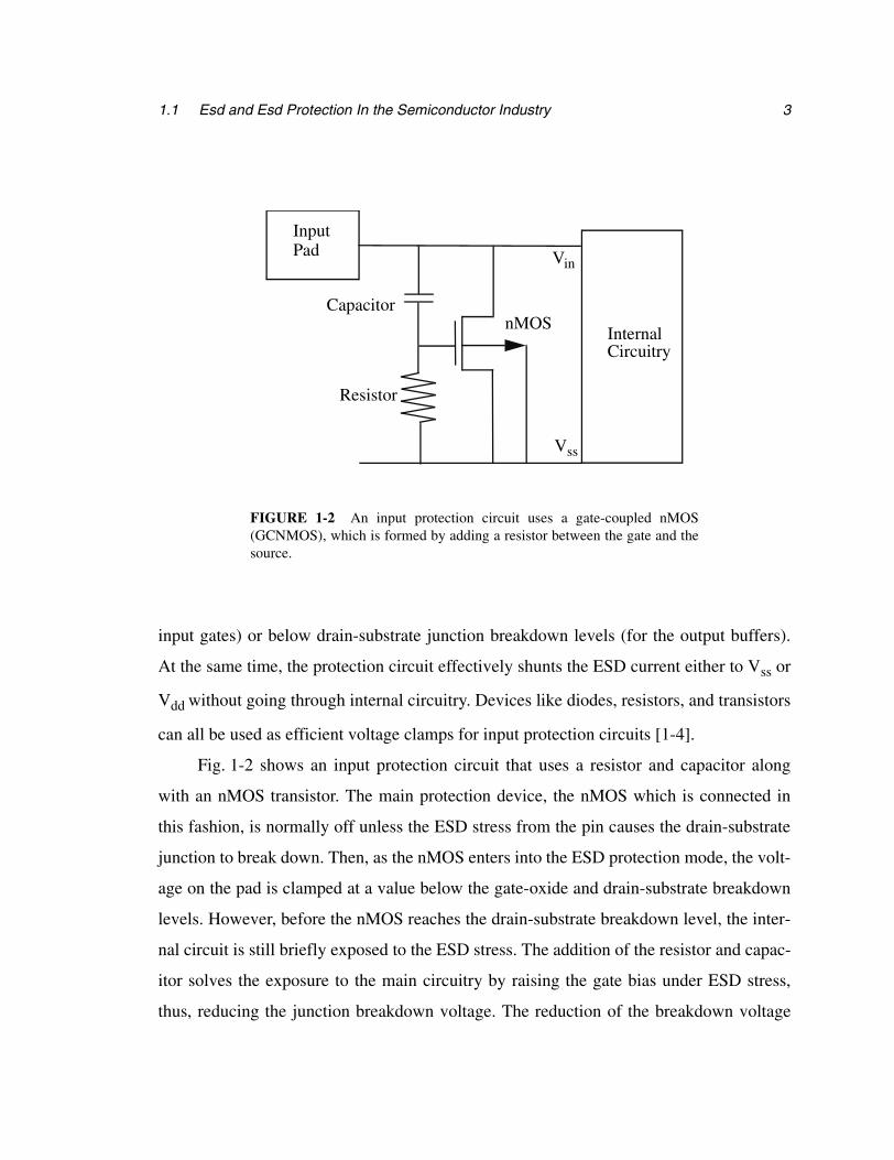
Fig. 1-2 shows an input protection circuit that uses a resistor and capacitor along
with an nMOS transistor. The main protection device, the nMOS which is connected in
this fashion, is normally off unless the ESD stress from the pin causes the drain-substrate
junction to break down. Then, as the nMOS enters into the ESD protection mode, the volt-
age on the pad is clamped at a value below the gate-oxide and drain-substrate breakdown
levels. However, before the nMOS reaches the drain-substrate breakdown level, the inter-
nal circuit is still briefly exposed to the ESD stress. The addition of the resistor and capac-
itor solves the exposure to the main circuitry by raising the gate bias under ESD stress,
thus, reducing the junction breakdown voltage. The reduction of the breakdown voltage
InputPad
Capacitor
Vin
Vss
Resistor
InternalCircuitry
nMOS
FIGURE 1-2 An input protection circuit uses a gate-coupled nMOS(GCNMOS), which is formed by adding a resistor between the gate and thesource.
CHAPTER 1 Introduction 4
also ensures the snapback of all the nMOS fingers; thus improving the current uniformity
during ESD stress. This scheme is called gate-coupled nMOS, GCNMOS [11-14].
The GCNMOS represents only one class of protection circuits; there are a variety of
other protection schemes. The silicon controlled rectifiers (SCRs) utilize latch-up to effi-
ciently conduct the stress current, obtaining lower clamping voltage [15-17]; the diode
networks connected between power supplies and I/Os use the forward bias mode to effi-
ciently conduct the high current [2,18]; the substrate pump circuits inject voltage or cur-
rent into the substrate to lower the trigger voltage [19-20], and the multi-sectional ESD
protection circuits use transmission line matching techniques at the operating frequency of
the IC to reduce the loading of the ESD protection circuit [21]. Ultimately, the specific
design of the protection circuits depends on the application.
1.2 THE IMPORTANCE OF MODELING ESD PROTECTION CIRCUITS
AND DEVICES
The development process in designing ESD protection circuits and devices has been
traditionally based on empirical and experimental research unlike the sophisticated model-
ing and simulation approach used for analog and digital circuit design. To optimize the
analog and digital circuit performance, the process technology has been tailored to achieve
the targeted device performance parameters in the normal operating region1; long-term
research enabled quantitative understanding of the device physics in the normal region so
that accurate circuit models can be developed with regard to geometry and process varia-
tions.2 We can then use the resulting circuit model to design and simulate the performance
1. In this context and throughout this thesis, the phrase, “normal operating region”, refers to the device operatingregions used for the analog and digital circuit designs; the operating region of the ESD protection devices are outsidewhat is considered to be the normal realm.
51.2 The Importance Of Modeling ESD Protection Circuits and Devices
of the core circuitry without relying exclusively on data from silicon for the whole design
process, thus, greatly reducing cost and shortening time to market.
Due to a lack of commercial ESD circuit models, the design of ESD protection cir-
cuits still relies on empirical results obtained from experimental data. Specific companies
have each developed their own in-house ESD models, but the models do not scale with
process and geometry. As a result, a large number of ESD devices must be fabricated and
measured to complete a set of circuit models that includes all the process and geometry
variations. For most companies, the typical design process for the protection circuits is a
trial and error procedure; many candidate circuits are ported into the new technology to be
fabricated, characterized, and evaluated for key ESD performance parameters, using
known testing techniques. Different combinations of device geometries fabricated on each
process variation are evaluated until a suitable protection circuit with the desired charac-
teristics is found [1,4].
Worse yet, a proven ESD protection circuit used in one technology generation can-
not be directly ported into the next generation without re-fabricating and re-testing
because the new process, which is only designed for the optimal normal device perfor-
mance, may adversely affect the performance of the ESD protection devices that operate
far from the normal region [22,23]. Furthermore, as the size of the bonding pads shrink
with each generation of technology, the size of the proven ESD protection circuits in the
previous generation of technology have to be scaled down due to the limitation posed by
the narrower pad pitch, causing an even greater reduction in performance. This is espe-
cially troublesome for fabless IC companies that rely on independent foundries for manu-
facturing since they cannot modify the processing steps to enhance ESD robustness.
Therefore, the testing of the ESD protection circuits can add significant cost and lead time
2. Within a state-of-the-art process, there are many process variations in terms of different substrate/well dopings toachieve different types of devices, such as lighter P-well doping and deeper junctions for the high voltage devicesimplemented in the I/Os, regular P-well doping for the internal circuitry, and lower channel implant for the lowthreshold devices providing more current drive, etc.
CHAPTER 1 Introduction 6
to the product development cycle. As a result, in an attempt to reduce the time delay and
cost, the protection circuits are directly imported into the chip from a previous technology
without silicon verification. But the finished chip may not pass the standard ESD test
required by the customer; thus, more money and time have to be spent to redesign the I/
Os.
A simulation-based approach, similar to the simulation-intensive approach for core
circuit design, can help designers to determine and understand the trade-offs among all the
design and technology parameters, thus rendering the whole ESD design process cost-
effective in materials and time. The obvious performance parameter that needs to be simu-
lated is the electro-thermal robustness of the ESD protection circuit, namely the amount of
current the protection devices can carry, or the amount of protection that can be offered,
before becoming irreversibly damaged. Many studies have been conducted in an attempt
to characterize and model the thermal run-away process based on the measured electrical
characteristics [1,4,24-27,32,47,53]. While the thermal run-away, or the second break-
down is the primary measurement for the robustness of ESD protection devices and cir-
cuit, it does not provide insight into the value of the clamping voltage, nor does it monitor
whether the circuit stays “off” or “on” during normal operation. Clearly, providing an
accurate basis for the electro-thermal action, the pure electrical characteristics of the pro-
tection element represent equally important performance parameters because the electrical
turn-on characteristics determine the interactions between the protection element and the
internal circuitry.
Ideally, the protection element should never interfere with normal circuit functions;
it should only turn on to protect the IC during the ESD stress. However, a poorly designed
protection circuit with low turn-on voltage activates during normal operations due to fluc-
tuations in the power supply. Conversely, devices with a high turn-on voltage activate too
late, causing damage to the internal circuit during an ESD stress. Therefore, an accurate
electrical circuit model of the ESD protection device not only can determine the function-
71.3 Previous Studies of the ESD Model and Existing Simulation Tools
ality of the protection circuit by simulating the electrical turn-on characteristics but also
can provide a good basis for the electro-thermal model [1,29-33].
Considerable progress has been made in the modeling of ESD protection devices
(see the next section and Chapter 2); however, the existing simulation methodology cannot
quantitatively characterize, model and simulate the geometry and process variations of the
protection devices. In addition, it is important to build geometric scaling capabilities into
the ESD model as experimental data has shown that there are key influences of electrical
characteristics resulting from changes in the layout. In order to address this problem, the
dissertation focuses on the modeling and characterizing of deep sub-micron ESD protec-
tion devices fabricated in the state-of-the-art CMOS technology. Emphasis is given to the
modeling of the substrate region, where the interactions with other circuit elements take
place. A Quasi-Mixed-Mode (QMM) device and circuit simulation methodology is devel-
oped to simulate the substrate resistance based on the layout; the resulting bulk resistance
is then used to simulate the high current characteristics of CMOS devices. The QMM
model possesses the scaling capabilities needed to capture the layout and process depen-
dencies. A three-dimensional substrate resistance model using a Pseudo-3D QMM model
is developed to simulate the substrate resistance in three dimensions (3D), expanding from
the simplified two-dimensional (2D) geometry. The goal of this work is to simulate the
electrical characteristics of protection devices, such as the clamping voltage or current,
using an approach based on simulation that augments the conventional test structure-based
approach.
1.3 PREVIOUS STUDIES OF THE ESD MODEL AND EXISTING
SIMULATION TOOLS
Existing compact models are first examined as a basis for building the layout depen-
dency. There are a number of similar compact models developed for the ESD protection
CHAPTER 1 Introduction 8
devices; they all capture the essential device physics in terms of modeling the junction
breakdown and the parasitic bipolar action [1,29,34-36]. While these studies have focused
on formulating the analytical equations for the junction breakdown and the parasitic bipo-
lar action used to fit the experimental data, the substrate resistance is crudely modeled
using only fixed resistance. Sktonici is one of the first to examine the role of the substrate
resistance during ESD stress [37]. Relying on experimental data and aided by device sim-
ulation, he concluded that the substrate resistance continues to decrease after the snapback
whereas previously researchers thought that the substrate resistance was constant for a
given device. The constant resistance assumption led to incorrect simulation results of the
substrate current, and consequently to incorrect simulation results of electro-thermal
robustness [37].
After Sktonici’s findings, researchers started to refine the ESD compact models to
include the reduction of the substrate resistance during snapback in order to accurately
estimate the current levels. Building on the compact model developed by Ameraskera and
Ramaswamy [29,34], their work uses a model of the nMOS device, operating in the ESD
regime and simulated using a normal MOSFET combined with a lateral NPN bipolar tran-
sistor. The normal MOSFET emulates the behavior of the device in the normal region; the
lateral NPN bipolar transistor models the snapback operation to achieve the low imped-
ance state for efficient current conduction. In addition, a dependent current source models
the junction breakdown process due to impact ionization; a voltage-controlled current
source models the substrate resistance. This simple model not only incorporates the sub-
strate resistance reduction model, but also demonstrates excellent agreement between the
simulation results using extracted parameters and the experimental data obtained from the
sub-micron devices in addition to a simple extraction method and characterization
method. However, the inability of the compact model to scale with layout seriously limits
its usefulness as reflected in the fixed substrate resistance and lateral bipolar parameters.
91.4 Outline
In order to model the layout dependency, device simulation is used to resolve the
scaling issues. Unlike lumped models used in the circuit simulation, the 2D and 3D
numerical device simulations allow the creation of 2D cross-sections or even 3D geometry
for a given semiconductor device with doping profiles, geometric definitions, and contact
placements. Applying appropriate bias conditions and the material/model coefficients, the
I-V characteristics of the device can be simulated. Moreover, Beebe’s curve tracing tech-
nique enables the automatic simulation of the snapback of the ESD I-V curve, allowing
the transition from the junction breakdown to the turn-on of the parasitic bipolar transistor
to be simulated with efficiency [4,39]. Various analysis capabilities also enable one to
study and examine properties at locations inside the device under arbitrary bias conditions,
including the distribution of the potential, current densities, electric field as well as impact
ionization generation rate, which is an important parameter for modeling junction break-
down for devices under the ESD stress [40]. Clearly, with these features, device simula-
tion can help promote understanding and analysis of device operation in the ESD region.
Combined results from both device and circuit simulation are used to model device
behavior. Devices for simulation are constructed, extracting the geometry (layout) depen-
dent parameters from supporting simulation results and abstracting the results into com-
pact model. A compact model is constructed knowing the interaction of the main device
and the parasitic device. A characterization method is also demonstrated to isolate and
extract parameters in the different physical regions1 of the device structures.
1.4 OUTLINE
This dissertation develops a new methodology for modeling and characterizing ESD
protection devices, focusing on the role of the substrate in the deep sub-micron CMOS
1. Our extraction methodology is based on the methodology formulated for obtaining the junction breakdown parame-ters. The detailed methodology is described in Chapter 2.
CHAPTER 1 Introduction 10
technology development. Unlike normal MOS operation, both the channel and substrate
regions in a given device need to be characterized and modeled to show that the current
extends from the channel into the substrate under ESD stress.
Chapter 2 describes the characterization, modeling, and implementation process in
the high-current regime for compact modeling based on a new implementation method
inside a commercial circuit simulator environment. The model parameters are extracted
from experimental data using a systematic methodology.
Chapter 3 describes work that extends the high-current regime model to enable sim-
ulation of effects that reflect the layout and process variations, specifically focusing on
modeling substrate resistance. Substrate resistance determines the on/off state of the pro-
tection device by providing a current discharge path from drain to substrate and from drain
to source. Substrate resistance also captures the substrate interactions between different
protection circuit elements. To characterize the sensitivity of substrate resistance, a new
methodology called Quasi-Mixed-Mode (QMM) is presented; the combination of device
and circuit simulation results are used in this new modeling approach.
Chapter 4 presents the application of the QMM model to the modeling of substrate
resistance for deep submicron ESD protection nMOS. The substrate resistance results
extracted by using this method show good agreement with values extracted from experi-
mental data. Limitations of the QMM method are discussed. The QMM method can only
model the substrate resistance of devices with width symmetry.1 The QMM method is
modified to enable the modeling of the substrate resistance of any device, including multi-
finger devices. The modified methodology is called Pseudo-3D Quasi-Mixed-Mode (P-3D
QMM).
Finally, Chapter 5 summarizes the contributions of the dissertation and discusses
future perspectives as well as the limitations of the current modeling efforts.
1. The term “width symmetry” is defined in Chapter 4.
CHAPTER 2
ESD DEVICE CHARACTERIZATION AND COMPACT MODEL
2.1 TYPES OF ESD STRESS
ESD stress is observed during the fabrication and packaging processes when a
charged object comes into contact with a chip, causing a high current discharge between
two pins. The ESD pulses can easily damage the circuits that are not properly protected.
Standardized test equipment has been developed to emulate real ESD events, reproducing
the stress environment and quantifying the resulting damage in a consistent manner. There
are three ESD test standards deriving from the following types of ESD pulses observed at
the chip level [41-43]:
1. The leading ESD test standard, the Human Body Model (HBM), also known as the fin-
ger model, simulates ESD stress generated by a charged human discharging through a
grounded chip.
11
CHAPTER 2 ESD Device Characterization and Compact Model 12
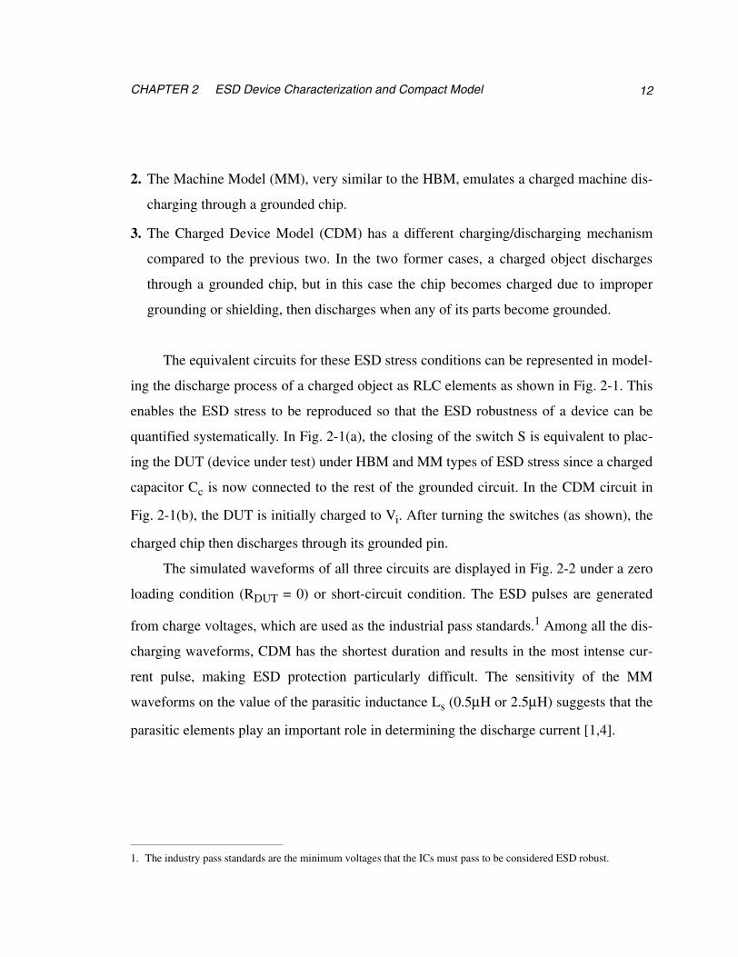
2. The Machine Model (MM), very similar to the HBM, emulates a charged machine dis-
charging through a grounded chip.
3. The Charged Device Model (CDM) has a different charging/discharging mechanism
compared to the previous two. In the two former cases, a charged object discharges
through a grounded chip, but in this case the chip becomes charged due to improper
grounding or shielding, then discharges when any of its parts become grounded.
The equivalent circuits for these ESD stress conditions can be represented in model-
ing the discharge process of a charged object as RLC elements as shown in Fig. 2-1. This
enables the ESD stress to be reproduced so that the ESD robustness of a device can be
quantified systematically. In Fig. 2-1(a), the closing of the switch S is equivalent to plac-
ing the DUT (device under test) under HBM and MM types of ESD stress since a charged
capacitor Cc is now connected to the rest of the grounded circuit. In the CDM circuit in
Fig. 2-1(b), the DUT is initially charged to Vi. After turning the switches (as shown), the
charged chip then discharges through its grounded pin.
The simulated waveforms of all three circuits are displayed in Fig. 2-2 under a zero
loading condition (RDUT = 0) or short-circuit condition. The ESD pulses are generated
from charge voltages, which are used as the industrial pass standards.1 Among all the dis-
charging waveforms, CDM has the shortest duration and results in the most intense cur-
rent pulse, making ESD protection particularly difficult. The sensitivity of the MM
waveforms on the value of the parasitic inductance Ls (0.5µH or 2.5µH) suggests that the
parasitic elements play an important role in determining the discharge current [1,4].
1. The industry pass standards are the minimum voltages that the ICs must pass to be considered ESD robust.

132.1 Types of ESD Stress
Rs
Ct DUT
LsS
Cc
+
-
Vc
Cc (pF) Ls (µH) Cs (pF) Rs (Ω) Ct
(pF)
HBM 100 7.5 1 1500 10
MM 200 2.5 1 5 10
DUT+
-
Vi
1MΩ 1Ω
50nH
Cs
FIGURE 2-1 (a) This is the lumped element circuit diagram for HBM and MM testers.Although the RLC discharging circuit is the same for HBM and MM, the magnitude of eachelement is quite different in each case, resulting in different current waveforms. (b) This isthe equivalent circuit schematic CDM.
(b)
(a)

CHAPTER 2 ESD Device Characterization and Compact Model 14
Cur
rent
(A
)
Cur
rent
(A
)
Cur
rent
(A
)
Time (ns)
Time (ns)Time (ns)(a) (c)
(b)
FIGURE 2-2 (a) HSPICE generated HBM waveform at 2000V under zero-load condition. (b)HSPICE generated MM waveform at 400V under zero-load condition. The shape of the waveform issensitive to the value of the inductance, with the solid curve generated from Ls=0.5µH and thedashed curve generated from Ls=2.5µH. (c) HSPICE generated CDM waveform at 1000V.
Ls=2.5µHLs=0.5µH
152.2 Device Operation
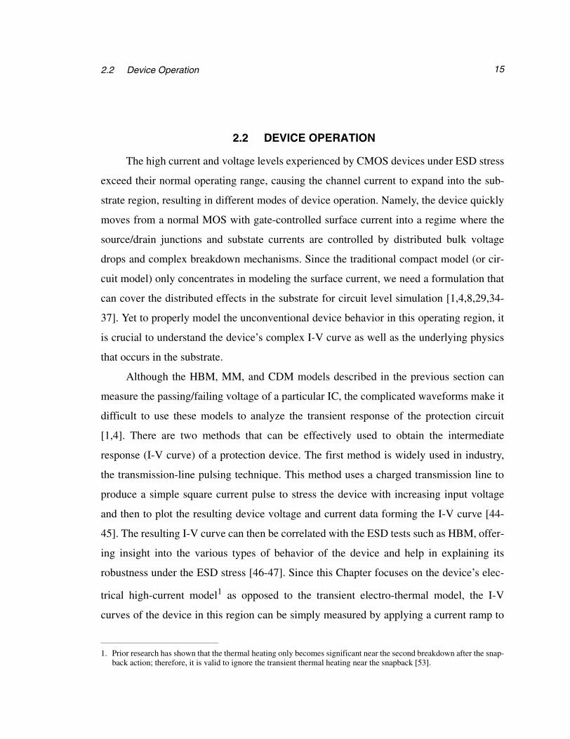
2.2 DEVICE OPERATION
The high current and voltage levels experienced by CMOS devices under ESD stress
exceed their normal operating range, causing the channel current to expand into the sub-
strate region, resulting in different modes of device operation. Namely, the device quickly
moves from a normal MOS with gate-controlled surface current into a regime where the
source/drain junctions and substate currents are controlled by distributed bulk voltage
drops and complex breakdown mechanisms. Since the traditional compact model (or cir-
cuit model) only concentrates in modeling the surface current, we need a formulation that
can cover the distributed effects in the substrate for circuit level simulation [1,4,8,29,34-
37]. Yet to properly model the unconventional device behavior in this operating region, it
is crucial to understand the device’s complex I-V curve as well as the underlying physics
that occurs in the substrate.
Although the HBM, MM, and CDM models described in the previous section can
measure the passing/failing voltage of a particular IC, the complicated waveforms make it
difficult to use these models to analyze the transient response of the protection circuit
[1,4]. There are two methods that can be effectively used to obtain the intermediate
response (I-V curve) of a protection device. The first method is widely used in industry,
the transmission-line pulsing technique. This method uses a charged transmission line to
produce a simple square current pulse to stress the device with increasing input voltage
and then to plot the resulting device voltage and current data forming the I-V curve [44-
45]. The resulting I-V curve can then be correlated with the ESD tests such as HBM, offer-
ing insight into the various types of behavior of the device and help in explaining its
robustness under the ESD stress [46-47]. Since this Chapter focuses on the device’s elec-
trical high-current model1 as opposed to the transient electro-thermal model, the I-V
curves of the device in this region can be simply measured by applying a current ramp to
1. Prior research has shown that the thermal heating only becomes significant near the second breakdown after the snap-back action; therefore, it is valid to ignore the transient thermal heating near the snapback [53].
CHAPTER 2 ESD Device Characterization and Compact Model 16
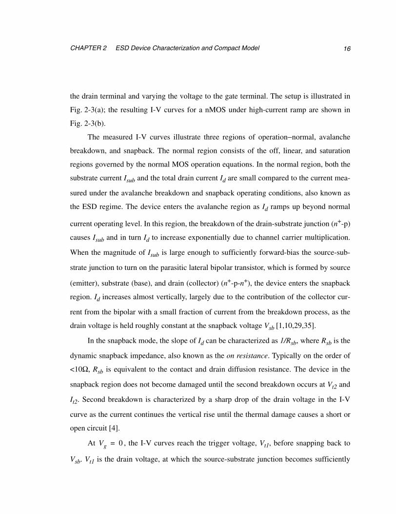
the drain terminal and varying the voltage to the gate terminal. The setup is illustrated in
Fig. 2-3(a); the resulting I-V curves for a nMOS under high-current ramp are shown in
Fig. 2-3(b).
The measured I-V curves illustrate three regions of operation−normal, avalanche
breakdown, and snapback. The normal region consists of the off, linear, and saturation
regions governed by the normal MOS operation equations. In the normal region, both the
substrate current Isub and the total drain current Id are small compared to the current mea-
sured under the avalanche breakdown and snapback operating conditions, also known as
the ESD regime. The device enters the avalanche region as Id ramps up beyond normal
current operating level. In this region, the breakdown of the drain-substrate junction (n+-p)
causes Isub and in turn Id to increase exponentially due to channel carrier multiplication.
When the magnitude of Isub is large enough to sufficiently forward-bias the source-sub-
strate junction to turn on the parasitic lateral bipolar transistor, which is formed by source
(emitter), substrate (base), and drain (collector) (n+-p-n+), the device enters the snapback
region. Id increases almost vertically, largely due to the contribution of the collector cur-
rent from the bipolar with a small fraction of current from the breakdown process, as the
drain voltage is held roughly constant at the snapback voltage Vsb [1,10,29,35].
In the snapback mode, the slope of Id can be characterized as 1/Rsb, where Rsb is the
dynamic snapback impedance, also known as the on resistance. Typically on the order of
<10Ω, Rsb is equivalent to the contact and drain diffusion resistance. The device in the
snapback region does not become damaged until the second breakdown occurs at Vt2 and
It2. Second breakdown is characterized by a sharp drop of the drain voltage in the I-V
curve as the current continues the vertical rise until the thermal damage causes a short or
open circuit [4].
At , the I-V curves reach the trigger voltage, Vt1, before snapping back to
Vsb. Vt1 is the drain voltage, at which the source-substrate junction becomes sufficiently
Vg 0=
172.2 Device Operation
forward biased as the bipolar carrier process sustains the breakdown process regenera-
tively. Moving from Vt1 to Vsb, the drain voltage reduces as current increases, producing a
negative resistance region, which also causes instability in the measurements. Stability is
achieved through the addition of a load resistance at the drain terminal. It is important to
note that the I-V curves for have a lower breakdown voltage than Vt1 at .
As shown in the GCNMOS example in Chapter 1, it is a property that circuit designers uti-
lize to reduce the stress on the core circuit by raising the gate voltage temporarily during
the ESD stress in an effort to reduce the breakdown voltage. The two-dimensional cross
section of a nMOS transistor shown in Fig. 2-4 includes the key circuit elements that help
to explain the decrease in the drain breakdown voltage under gate control along with the
underlying physic effects associated with these I-V curves [1,29,34,35].
As Id ramps up for a device in the off state, avalanche multiplication occurs in the
drain junction when the electric field associated with the rising drain voltage begins to
exceed a certain threshold. Namely, the electric field around the drain junction reaches the
point where electrons (for nMOS) gain enough energy to create electron-hole pairs during
the collision process. Many additional electron-hole pairs are generated from this multipli-
cation process, hence, the term avalanche [48]. The electron component of the current
travels directly into the drain terminal as Id, while the hole current Igen flows toward the
substrate contact, becoming the substrate current, Isub. The magnitude of Isub increases
exponentially during avalanche breakdown, shifting the action away from the channel and
into the substrate.
Potential builds up inside the substrate due to the voltage drop across the substrate
resistance Rsub generated by Isub. When the substrate potential, Vsub, reaches the forward
bias voltage of the substrate to source diode, the parasitic bipolar transistor is turned on,
causing the device to enter the snapback region. Once in the snapback region, Igen splits
into two paths, one component is Isub and the other becomes base current, Ib, flowing in
Vg Vth> Vg 0=

CHAPTER 2 ESD Device Characterization and Compact Model 18
HP4145
(a)
(b)
FIGURE 2-3 (a) HP4145 parameter analyzer can be used to measure high I-V data forMOSFETs. (b) The I-V curves of nMOS with different regions of operation labeled includingthe second breakdown are obtained using the set-up shown in (a). The plot on the left is Id vs.Vd, and the plot on the right is ln Isub vs. Vd.
Vsb
Vt1
snapback region
Vg=3.3V
Vg=1.5V
Vg=0V
snapback region
Vt1
Vsb
avalanche avalanche region
DUT
Id
Isub
Vg
normal region
Rload
region
Vd (v)
I d (
A)
ln I s
ub (
A)
Vd (v)
1/Rsb
Vt2, It2
second breakdown
192.3 Compact Model for Transistors
the opposite direction. The current Id is mainly sustained by the bipolar transistor action
instead of solely relying on the avalanche breakdown; thus, Vd can be decreased from Vt1
to Vsb and still support the same level of Id. At this point, the device can carry large
amounts of drain current while holding the voltage at roughly Vsb. The protection device
should operate in the snapback region in order to clamp the voltage at Vsb and to provide a
low resistive path for discharging the ESD current. However, the increased number of car-
riers flowing into the substrate from the emitter modulate Rsub, causing a reduction of its
magnitude. This is a negative feedback effect on the bipolar injection process since
reduced Rsub tends to decrease the forward bias on the source-substrate junction, which
then leads to an increase of Isub in the snapback region to maintain the forward bias
[34,37].
Considering the same device with gate control, the magnitude of Ids (compared to Ids
at leakage current level) may be large enough to generate adequate hole current to for-
ward-bias the substrate-source junction at much lower drain electric field, which explains
the I-V curve behavior at moving from avalanche to snapback region without
needing the high electric field at Vt1.
In both cases, as Id and Isub continue to increase, there will be Joule heating ( )
inside the device that will cause the device to overheat to the point of thermal runaway or
the second breakdown, where it will suffer permanent damage [1,4,26,27,53].
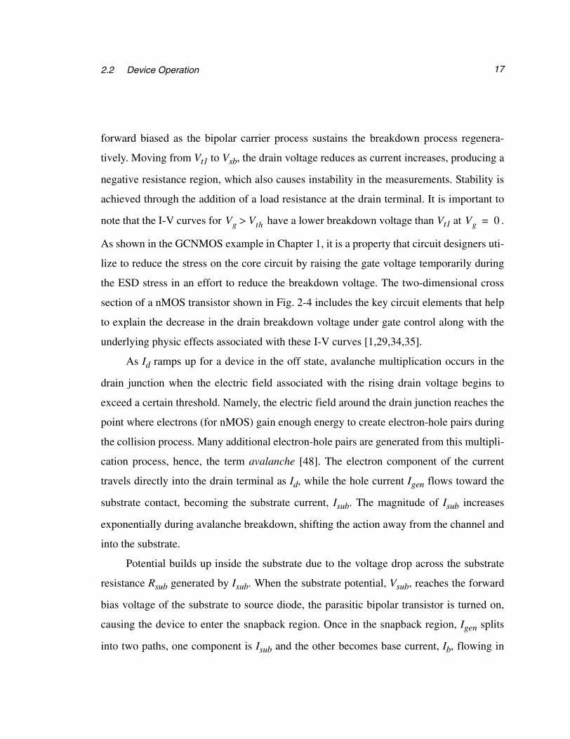
2.3 COMPACT MODEL FOR TRANSISTORS
ESD operations occur during the avalanche breakdown and snapback modes; hence,
standard compact models for simulation of the normal operation need to be extended to
simulate the high-current characteristics of the MOSFET protection device. Model exten-
Vg Vth>
J ε⋅
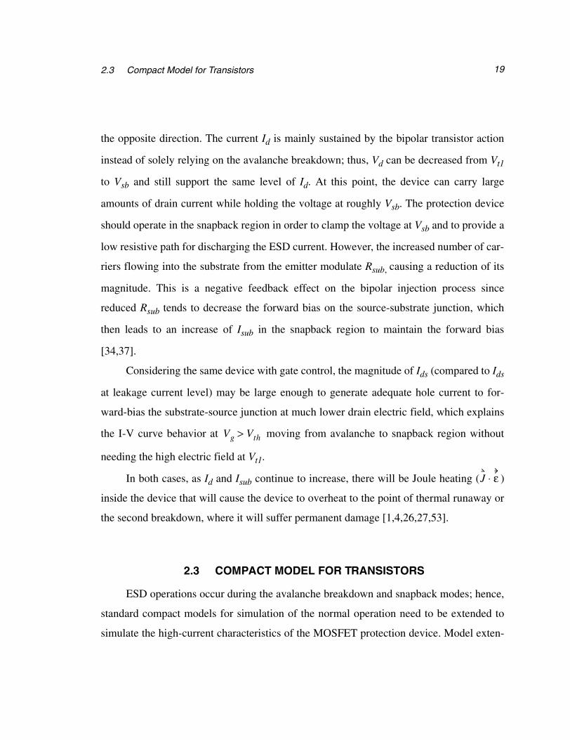
CHAPTER 2 ESD Device Characterization and Compact Model 20
sions should include the avalanche multiplication during breakdown, substrate resistance
effects needed to generate the base potential, and BJT operation under snapback.
Analytical models for the ESD region have been developed to formulate the analyti-
cal avalanche breakdown expressions as well as to model the parasitic BJT and Rsub
[35,49-52]. While demonstrating good fit-to-data results, the models are not applicable to
submicron devices since they are developed for classical long channel technologies (in >1
µm range) with simpler process technologies. Improving upon the long-channel model,
excellent advances have also been made in developing electrical circuit-level models for
+
-
RsubVsub
Ids (e-)
Ic (e-)
Igen (e+)
Ib (e+)
Isub (e+)
Drain
Id
Source
Gate
Substrate
FIGURE 2-4 The two-dimensional cross section of a nMOS illustrates thedevice operation under high current stress. The hole current is drawn in gray,and the electron current is shown in black. The direction of the arrows drawnfor Ids and Ic shows the direction of electron flow.

212.3 Compact Model for Transistors
short-channel devices in more advanced CMOS technologies, demonstrating good agree-
ment with experimental data and containing the essential physics [29,34,36]. Illustrated in
Fig. 2-5, this circuit level model extends and complements the work of Amerasekera and
Ramaswamy in the areas of substrate resistance modeling, extraction of avalanche model
parameters, as well as the implementation methodology while adopting previous ava-
lanche and parasitic BJT formulations.
The model shows a standard nMOS with drain/source diffusion and contact resis-
tance rd and rs, modeling the normal transistor operating regions−linear, saturation, and off
state. The nMOS is connected in parallel with a bipolar transistor, modeling the parasitic
BJT in the snapback region. Representing hole current generated from avalanche multipli-
cation, a current-controlled current source Igen couples the drain/collector terminals to a
variable substrate resistor, Rsub. Rsub is the conductivity-modulated substrate resistance,
whose product with Isub determines the magnitude of Vsub and the on/off state of the para-
sitic bipolar transistor.
This model simulates a positive feedback process that starts with the avalanche mul-
tiplication process at the drain junction, which then causes the voltage to be dropped
across Rsub to forward-bias the source-substrate junction, finally leading to the turn-on of
the bipolar transistor. As this positive feedback process couples all the parameters
together, it becomes difficult to physically isolate one parameter from another during the
modeling and characterization process. To address the challenges in parameter extraction
associated with coupled device behavior, a substrate resistance model is formulated to
decouple the nMOS and BJT, thereby simplifying the characterization process. In addi-
tion, systematic extraction procedures also help to decouple the interlinked parameters.
This decoupling methodology will be described further in this chapter and in Chapter 3.
As shown in the compact model, Id is composed of three contributions
Id Ids Ic Igen+ += (2.1)
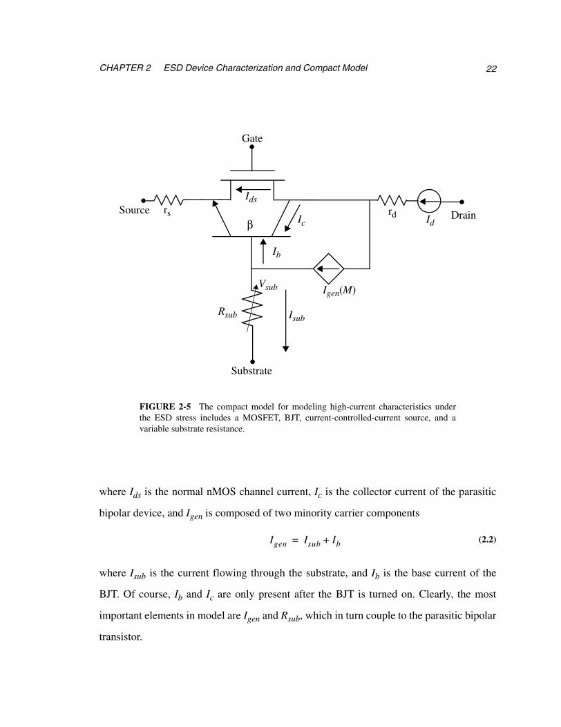
CHAPTER 2 ESD Device Characterization and Compact Model 22
where Ids is the normal nMOS channel current, Ic is the collector current of the parasitic
bipolar device, and Igen is composed of two minority carrier components
where Isub is the current flowing through the substrate, and Ib is the base current of the
BJT. Of course, Ib and Ic are only present after the BJT is turned on. Clearly, the most
important elements in model are Igen and Rsub, which in turn couple to the parasitic bipolar
transistor.
Igen Isub Ib+= (2.2)
Igen(M)Vsub
Id
IdsSource Drain
Gate
Substrate
Ib
Isub
Ic
Rsub
β
FIGURE 2-5 The compact model for modeling high-current characteristics underthe ESD stress includes a MOSFET, BJT, current-controlled-current source, and avariable substrate resistance.
rs rd
232.4 Modeling of igen and M
2.4 MODELING OF Igen AND M
Modeling the avalanche breakdown process, one has to formulate Igen differently,
depending on the on/off state of the BJT. Before the bipolar turns on, Igen is modeled as
[29]
where Ids is the electron source (for nMOS) that initiates the avalanche multiplication.
After the bipolar device turns on, generation can be modeled as
where the sum of the electron current, , is available for the hole generation pro-
cess. M is present in both equations, namely the hot-carrier region (weak avalanche),
where the drain bias is within the operating range and the strong avalanche region, where
the drain bias exceeds the operating voltage under the ESD stress. M, the avalanche multi-
plication factor, is defined as the ratio of the total number of electrons after avalanche
breakdown to the initial number of electrons before the breakdown. The high electric field
inside the drain depletion region causes the incoming electrons (n0) to gain enough energy
to generate electron/hole pairs, thereby creating a larger number of electrons (nf) that exit
the depletion region. The magnitude of M is determined by the rate of impact ionization, α
[48]
where χd represents the width of the depletion region, and α depends on the magnitude of
the electric field at the drain junction.
Igen M 1–( ) Ids⋅= (2.3)
Igen M 1–( ) Ids Ic+( )⋅= (2.4)
Ids Ic+
Mnf
n0----- 1
1 α xd0
χd
∫–
--------------------------= = (2.5)
CHAPTER 2 ESD Device Characterization and Compact Model 24
Although α depends on the electric (Ε) field in a complex and multi-dimensional
way, several analytical models have been developed to simplify that relationship
[35,48,54-57]. A majority of the expressions are modifications based on the well-known
Chynoweth formula
where A and B are the ionization constants, Ε is the peak electric field inside the effective
ionization length, ld, (as opposed to the depletion region near the drain)
where Vd is the drain terminal voltage, Vdsat is the voltage at velocity saturation. For
graded junctions such as LDD, the Ε field varies significantly across the depletion region;
therefore, based on eqs. (2.3), (2.5) and (2.6), small errors in the calculations of the Ε field
can lead to gross errors in Isub due to the exponential dependency of α on Ε. To obtain an
accurate expression for α, the expression of Ε field is modified in terms of drain voltages
and ld, which are derived based on 2D numerical simulation and subsequent parameteriza-
tion. The resulting analytical α expessions require a large number of fitting parameters to
properly model the data, complicating the extraction process. Moreover, these formula-
tions have mainly been developed to model hot carrier phenomena in the saturation region
[35,54-56]. While they are good at modeling the peak Isub (in Isub vs. Vg) in weak ava-
lanche region, the modeling of Isub in the ESD regime remains only an approximation
[34].
Okuto and Crowell [57] developed an analytical expression of α for the purpose to
model junction breakdown; hence, it was chosen by Ramaswamy et. al. [36] to model the
α ABE---–
exp⋅= (2.6)
EVd Vdsat–
ld------------------------≈ (2.7)
252.4 Modeling of igen and M
avalanche breakdown occurring inside the ESD region. Ramaswamy proceeded to demon-
strate good agreement between the model and experimental data, thus motivating the
adoption of the formulation for the modeling of M in this thesis. The equation is obtained
by simplifying the precise expression for the nonlocalized ionization coefficient [57]
where A, B, m, and n are empirical constants that model non-local dependence of α on the
electric field, Ε, inside the depletion region. This expression reduces to Eq. (2.6) when m
and n are taken to be 0 and 1 respectively, which is adequate for abrupt junction as Ε field
is roughly constant across the depletion region. The Ε field can be modeled similarly to
Eq. (2.7)]
where Vd is the voltage at the drain terminal, Vdch is the channel voltage near the drain,
and χd is the width of the depletion region, which is used instead of the effective ioniza-
tion length, ld for the condition of strong impact ionizaton.
α A Em B
En
------–exp⋅ ⋅= (2.8)
EVd Vdch–
χd-----------------------= (2.9)
CHAPTER 2 ESD Device Characterization and Compact Model 26
Substituting the expression for the Ε field in Eq. (2.9) and α in Eq. (2.8) into Eq.
(2.5), the overall expression for M becomes [34]
where Ai and Bi, the empirically chosen parameters, are related to the impact ionization
rate A and B through χd as follows: and .
The parameter Vdch models the effect of the gate bias on the Ε field. Naturally, Vdch
is zero when there is no gate bias; Vdch increases with the gate voltage. As a result, the
magnitude of M is reduced due to availability of more Ids for the hole generation at higher
Vg values. The Vdch term again becomes zero after the bipolar device turns on due to neg-
ligible gate influence. The magnitude of Vdch not only depends on gate bias, but also var-
ies with the channel length, L [34,58]
where is the effective gate bias, Abulk is a fitting parameter, and Εsat is the elec-
tric field at which velocity saturation occurs for the carriers.
The M expression implies that its magnitude depends mostly on the specific process
technology; it is not influenced by the device geometry, not even channel length. The
drain doping profile and junction are technology variables that influence M by determin-
ing the channel Ε field. The parameters Ai, Bi, m, and n are related to the technology. Ai
M1
1 Ai Vd Vdch–( )m Bi
Vd Vdch–( )n---------------------------–exp⋅ ⋅–
------------------------------------------------------------------------------------------------------------= (2.10)
Ai A χd⋅≈ Bi B χd⋅≈
Vdch
Vgs Vth–
Abulk
Vgs Vth–
Esat L⋅---------------------+
----------------------------------------= (2.11)
Vgs Vth–
272.5 Extraction Methodology for M Parameters
and Bi are determined by the depletion width and ionization coefficient; m and n are
empirically shown to be dependent on drain junction profiles [57]. Modeling the influence
of the gate, Vdch is the only parameter that shows channel length dependency, but it can be
extracted without taking data into the snapback region. Therefore, the parameters for M
only need to be extracted once for each specific process.
2.5 EXTRACTION METHODOLOGY FOR M PARAMETERS
We need to extract the M parameters from experimental data in order to effectively
model the junction breakdown of a nMOS under ESD stress. The values of the parameters
can be used to provide insight into the scaling issues. We aim to develop an accurate and
reproducible extraction methodology in order to connect the model parameters to physi-
cally meaningful quantities.
For extraction purposes, only one measurement is needed using an HP4145; the
setup is illustrated in Fig. 2-3 (a). A high-current measurement is made by ramping the
drain current until the snapback happens at each gate bias. The result is a family of I-V
curves as shown in Fig. 2-3 (b). The I-V data are separated into the regions before and
after snapback for the extraction purpose. In order to decouple M parameters from the
bipolar parameters and substrate resistance, we extract the parameters associated with M
in the breakdown region, where the impact ionization dominates prior to the turn-on of the
bipolar device in the snapback region.
To implement Igen, only the parameters related to M need to be extracted. Recall that
the M expression described in the last section has the form
M1
1 Ai Vd Vdch–( )m Bi
Vd Vdch–( )n------------------------------–exp–
-----------------------------------------------------------------------------------------------=

CHAPTER 2 ESD Device Characterization and Compact Model 28
where Ai, Bi, and Vdch are the key parameters to be extracted.
Ramaswamy et. al. extracted Ai, Bi, and Vdch by solving a set of coupled equations to
obtain a non-linear equation in Vdch. Taken in weak-avalanche region, the peak Isub/Vg
point on the Isub vs. Vg curves at a given drain bias can be used to solve the Vdch values for
that Vg point. Other model parameters can then be computed from each value of Vdch. This
extraction method was reported as a means to fit the experimental data for both weak and
strong avalanche breakdown regions [34]. However, the calculations can be quite messy
due to the non-linear nature of the equation; in addition, to obtain values of Vdch for lower-
gate biases, the Isub vs. Vg curve had to be taken at a drain bias lower than the power sup-
ply, resulting in a much flatter curvature with multiple peaks, in contrast to the sharp cur-
vature with a clear peak observed at higher-drain biases. For lower-gate bias, choosing the
wrong peak Isub/Vg values can cause inaccuracies in the calculation of Vdch, which then
propagate to the other M parameters, resulting in erroneous extraction of M parameters.
Instead of using only the peak values, we propose to adopt a simpler graphical
extraction method that uses all the data points before the snapback to extract M parame-
ters, which will fit the experimental data globally. Vdch is extracted first since it can be
independently determined. This is an important step because not only the exponential rise
of Isub depends on Vdch through M, but also the extractions of Bi are directly based on Vdch
values. Vdch models the effect of gate bias on impact ionization; it is the equivalent thresh-
old voltage for impact ionization. For short channel devices, this threshold is controlled by
velocity saturation rather than by pinch-off. Unfortunately, the transition from the linear to
saturation region is very smooth, making it difficult to determine where the impact ioniza-
tion occurs based solely on examining the Id vs. Vd curve.
Several graphical methods for extracting Vdch were considered [8,55,59-60]. Pro-
posed by Jang et. al., this extraction method is derived from the device theory expressing
the drain current as a function of the drain voltage [59]. The method seems to be the most

292.5 Extraction Methodology for M Parameters
promising at first since the device theory is independent of any specific device. However,
taking the graphical derivative of 1/gds from the experimental Id vs. Vd data generates con-
siderable numerical noise, rendering it nearly impossible to locate Vdch graphically, espe-
cially for small values of the derivative. The extraction method developed by Chan et. al.
was adopted since this method fits the definition of Vdch as a threshold voltage for the
impact ionization process by utilizing the impact-ionization current, Isub, to extrapolate for
Vdch [60]. Moreover, the method is simple to implement.
The only measurement curves needed for Vdch extractions are Id vs. Vd and Isub vs.
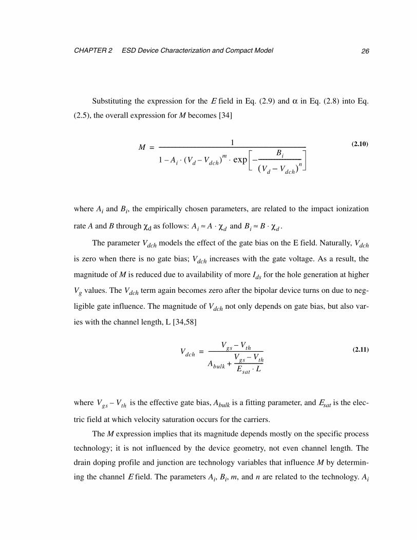
Vd, taken before snapback at different gate biases.The entire extraction process for Vdch
values across all gate biases is illustrated in Fig. 2-6. In the breakdown region of the
experimental Id vs. Vd curves, curve A is formed by tracing different data points to
yield the same ratio of for all values of Vg. The ratio of is taken to be
about 0.01 in this case. Ideally, any ratio of can be used to trace out curves parallel
to curve A, but in reality, the range of ratios is more limited by the resolution of Isub data
taken at low-gate bias. Using Eqs. (2.1-3), the form can also be represented in
terms of M as ; hence, curve A actually connects the drain voltages that have the
same impact ionization across the gate bias.
Owing to the noisy Isub measurement taken at drain voltages much lower than junc-
tion breakdown at , we concluded that the x-intercept of curve A should be
obtained from data at instead of [61]. Although clear Isub
measurements can be made in the snapback region at , the resulting Isub would be
a mixture of impact ionization and bipolar current, not suitable for extracting impact ion-
ization. By picking a smaller ratio than 0.01, the diode-like curve A will shift
Vd Id⁄
Isub Id⁄ Isub Id⁄
Isub Id⁄
Isub Id⁄
M 1–M
--------------
Vg 0=
Isub Id⁄ Vg Vth= Vg 0=
Vg 0=
Isub Id⁄
CHAPTER 2 ESD Device Characterization and Compact Model 30
toward the origin, and for a ratio of zero, the curve will be shifted exactly to the origin;
thus, curve B maps out Vdch values which indicates the occurrence of impact ionization.
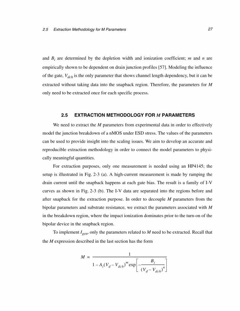
The intersection points between curve B and the Id. vs. Vd curves are Vdch values for all
Vgs as shown in Fig. 2-7. The solid curve in the figure represents the extracted Vdch values
from the 0.35µm device in Fig. 2-6; the dashed curve maps out the Vdch values from the
0.55µm device. As expected, both sets of Vdch values rise with Vg due to increasing levels
of gate control. The 0.55µm device has higher Vdch values, especially at higher gate
biases, closely approximating the classical pinch-off definition of the saturation voltage.
curve A
curve B
Extracted Vdch for each Vg
Vd (V)
I d (A
)
FIGURE 2-6 The extraction process of Vdch for a 0.35µm device with Id vs. Vd at Vg=0.9, 1.5,
2.1, 2.7, and 3.3V. Vdch at each Vg is the intercept of curve B with Id vs. Vd plot.
312.5 Extraction Methodology for M Parameters
Conversely, the slope of the Vdch curve of the 0.35µm device decreases at the high gate
biases, demonstrating the velocity-saturation phenomena for the short channel devices.
The Ai and Bi parameters are extracted next. They are determined by the impact ion-
ization constants A, B and χd, as discussed previously. More recently, Slotboom et. al.
measured and published values for A and B in bulk silicon as well as the silicon-silicon-
dioxide interface [62-63]. Since impact ionization can occur either at the silicon surface or
(V)
Vdc
h (V
)
FIGURE 2-7 The extracted Vdchs for the 0.35µm device across effective gate biases are
plotted in circles, and the solid line is used to interpolate the Vdch values between the extractedvalues.The extracted Vdchs for the 0.55µm device across effective gate biases are plotted incircles with the dotted line.
Vg Vth–
0.35µm
0.55µm
CHAPTER 2 ESD Device Characterization and Compact Model 32
in the bulk near the LDD/n+ junction; it is not clear which values to choose for A and B.
Futhermore, χd still needs to be extracted from the experimental data. To simplify the
extraction process, the Ai and Bi parameters are extracted directly from the experimental
data.
To facilitate the extraction and to linearize Bi with respect to the exponential term,
the M equation is rewritten as [61]
Bi can then be extracted as the slope resulting from plotting the data as vs.
for all Vg. Since Vdch values have already been extracted, the expression
can be easily graphed. The experimental data can also be plotted in the
form of because M, the multiplication factor, can be defined in terms of theexperimental data as
Hence, substituting the above equation, can be expressed as
Fig. 2-8 is obtained by plotting the data as vs. ; Bi can be
extracted from the slope. The curve for each Vg fall virtually on top of each other, demon-
11M-----–
ln Ai Vd Vdch–( )m⋅[ ]lnBi–
Vd Vdch–( )n------------------------------+= (2.12)
1 1 M⁄–( )ln
1 Vd Vdch–( )n⁄
1 Vd Vdch–( )n⁄
1 1 M⁄–( )ln
MId
Id Isub–-------------------= (2.13)
11M-----–
ln
11M-----–
lnId
Isub---------ln= (2.14)
11M-----–
ln1
Vd Vdch–( )n------------------------------
332.5 Extraction Methodology for M Parameters
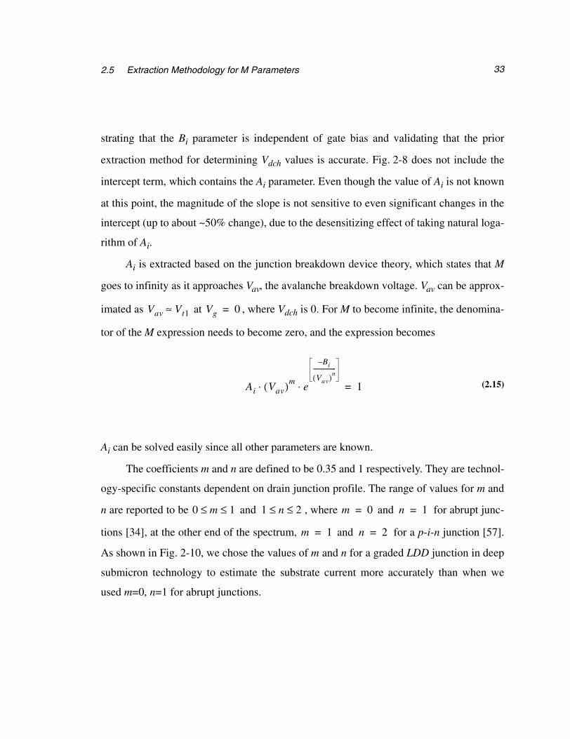
strating that the Bi parameter is independent of gate bias and validating that the prior
extraction method for determining Vdch values is accurate. Fig. 2-8 does not include the
intercept term, which contains the Ai parameter. Even though the value of Ai is not known
at this point, the magnitude of the slope is not sensitive to even significant changes in the
intercept (up to about ~50% change), due to the desensitizing effect of taking natural loga-
rithm of Ai.
Ai is extracted based on the junction breakdown device theory, which states that M
goes to infinity as it approaches Vav, the avalanche breakdown voltage. Vav can be approx-
imated as at , where Vdch is 0. For M to become infinite, the denomina-
tor of the M expression needs to become zero, and the expression becomes
Ai can be solved easily since all other parameters are known.
The coefficients m and n are defined to be 0.35 and 1 respectively. They are technol-
ogy-specific constants dependent on drain junction profile. The range of values for m and
n are reported to be and , where and for abrupt junc-
tions [34], at the other end of the spectrum, and for a p-i-n junction [57].
As shown in Fig. 2-10, we chose the values of m and n for a graded LDD junction in deep
submicron technology to estimate the substrate current more accurately than when we
used m=0, n=1 for abrupt junctions.
Vav Vt1≈ Vg 0=
Ai Vav( )me
Bi–
Vav( )n----------------
⋅ ⋅ 1= (2.15)
0 m 1≤ ≤ 1 n 2≤ ≤ m 0= n 1=
m 1= n 2=
CHAPTER 2 ESD Device Characterization and Compact Model 34
Finally, M can be calculated using the extracted values; the calculated M curves are
compared to the experimentally determined M as shown in Fig. 2-9. The extracted param-
eters Ai, Bi, m, and n for the devices A and B with different gate lengths in 0.35µm CMOS
technology are summarized in Table 2-1.
1
Vd Vdch–( )n------------------------------
11 M-----
–
ln
snapback region
Slope is Bi
FIGURE 2-8 These data points are formed by graphing all the data at each Vg before snapback.
This slope is Bi.

352.5 Extraction Methodology for M Parameters
Devices Extracted M parameters
Ai Bi m n
0.35µm 4.5 24 0.35 1
0.55µm 4 22 0.35 1
TABLE 2-1 M parameters’ values for 0.35µm and 0.55µm devices
Vd (V)
M (
A/A
)
Vg=0.9V
Vg=1.5V
Vg=2.1V
Vg=2.7V
Vg=3.3V
FIGURE 2-9 The comparison between calculated M (solid line) from extractedparameters and the experimental M obtained from the data.
CHAPTER 2 ESD Device Characterization and Compact Model 36
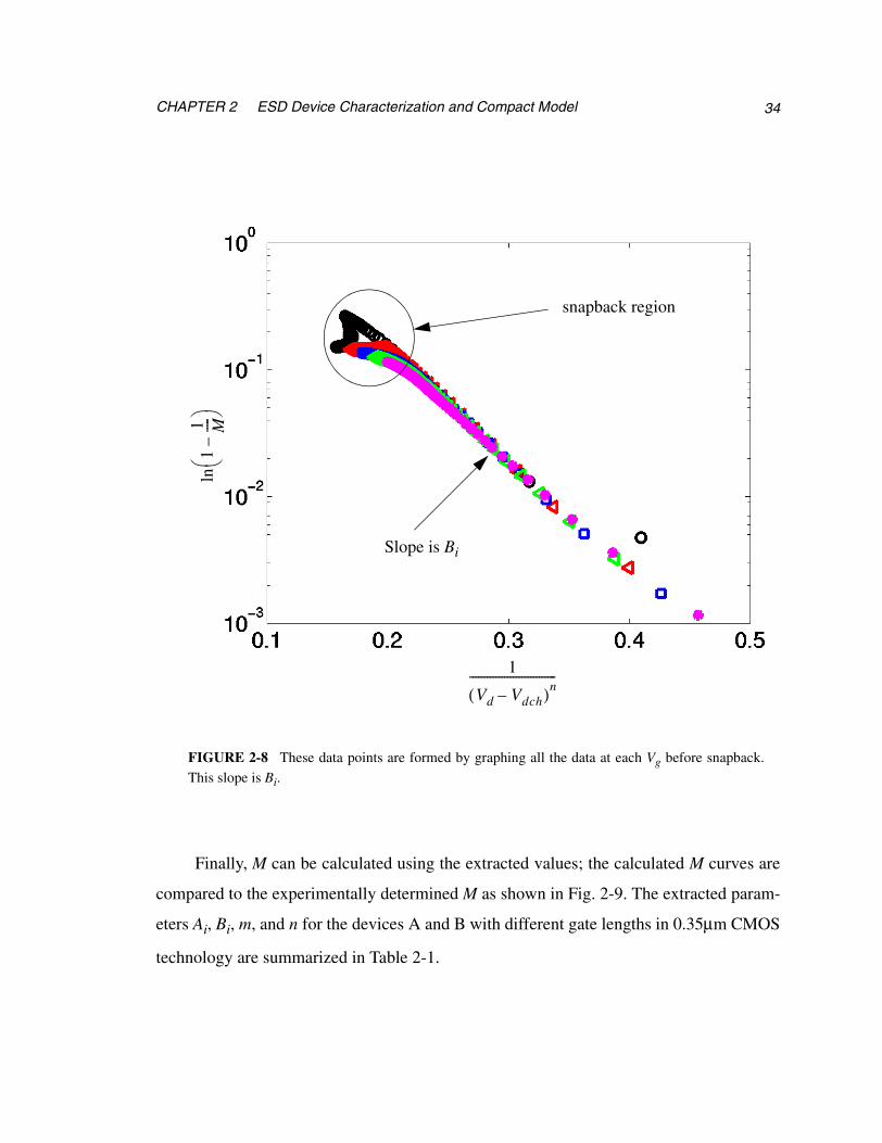
Despite the channel length differences, the similarity of the extracted M values dem-
onstrates that the junction breakdown (M) is a process dependent event; hence, only one
set of M parameters is needed for a given process. Furthermore, since only a small range
of channel lengths will be used in I/O circuit design, an optimal set of M parameters can be
easily found to fit the experimental data.
2.6 SUBSTRATE RESISTANCE MODEL
In the previous section, the assumption was made to extract Ai. Although
the two voltages are similar in magnitude, there is a subtle difference between the defini-
tions of Vav and Vt1. Vav is defined as the junction breakdown voltage, at which point the
parasitic bipolar is still off, ; Vt1 is the trigger voltage, at which point
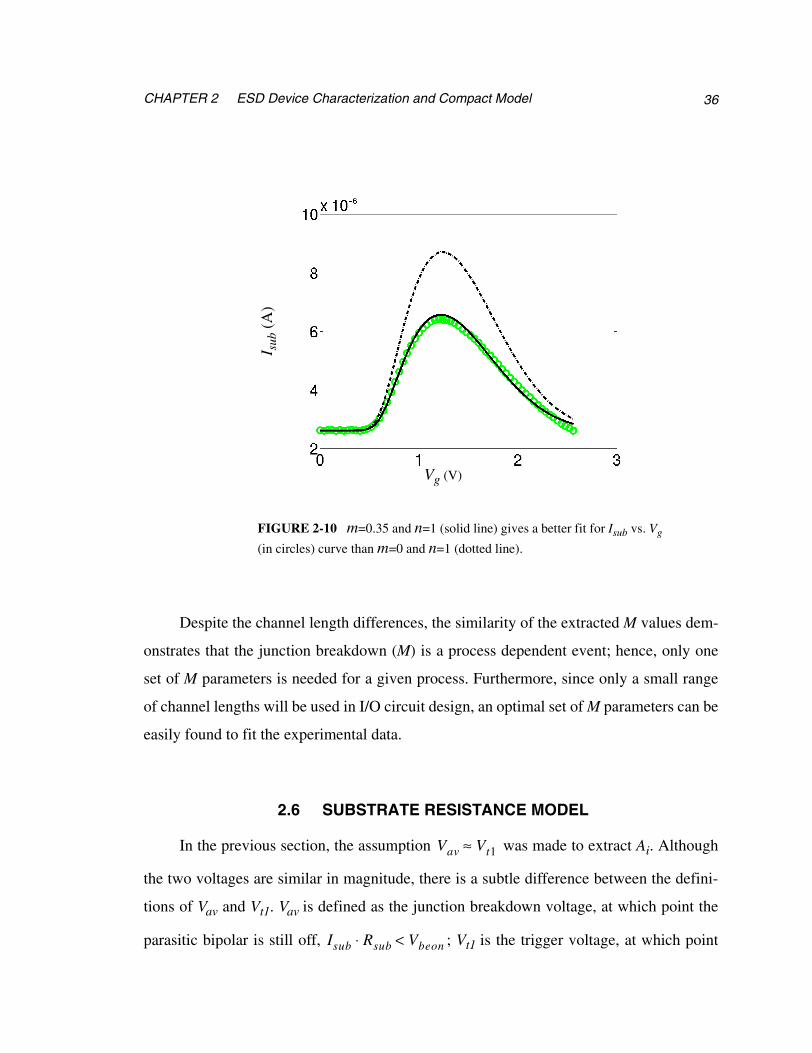
FIGURE 2-10 m=0.35 and n=1 (solid line) gives a better fit for Isub vs. Vg
(in circles) curve than m=0 and n=1 (dotted line).
Vg (V)
I sub
(A
)
Vav Vt1≈
Isub Rsub⋅ Vbeon<
372.6 Substrate Resistance Model
the bipolar device begins to turn on, . Despite the subtle difference, Vt1
is still a good approximation since a majority of hole current is generated at Vav that turns
on the bipolar immediately [1,10]. At the Vav point, the exact magnitude of the substrate
resistance is not critical since the generated substrate current dominates. However, this
only holds true at ; for , as the generation process relies more on the initial
drain current and less on the drain voltage, the magnitude of the substrate resistance
becomes important in determining the on/off state of the parasitic bipolar transistor.
Therefore, accurate modeling of the substrate resistance is essential for the simulation and
design of the ESD protection circuits. Moreover, in order to simulate the substrate current
correctly, we also need to account for the fact that the substrate resistance becomes con-
ductivity modulated due to the injection of minority carriers into the base after the turn-on
of the parasitic BJT [34,37].1
The effects of conductivity modulation can be seen from the experimental data as
shown in Fig. 2-3(b). The data shows that the substrate current continues to increase even
after snapback; therefore, to maintain a constant base-emitter voltage, the substrate resis-
tance must decrease. This can be explained by high-level injection of electrons from the
emitter (source) to the base (substrate) that conductively modulates the substrate resis-
tance, causing this reduction.
Previously, a single constant valued resistor was used to model the substrate
[29,35,36]. The magnitude of the resistance is extracted at the on-state during snapback.
While the single resistance accurately estimates the device behavior up to the point of
snapback, the conductivity modulation that happened afterwards is not accounted for,
resulting in an overestimation of the substrate resistance and underestimation of the sub-
strate current, which can lead to inaccurate simulation results for the second breakdown as
1. The interactions between the substrate resistance for multi-finger ESD protection devices will be discussed in detail in the Chapter 4. In this chapter, we discuss only the single-finger individual protection devices in relation to the sub-strate resistance.
Isub Rsub⋅ Vbeon≈
Vg 0= Vg 0>
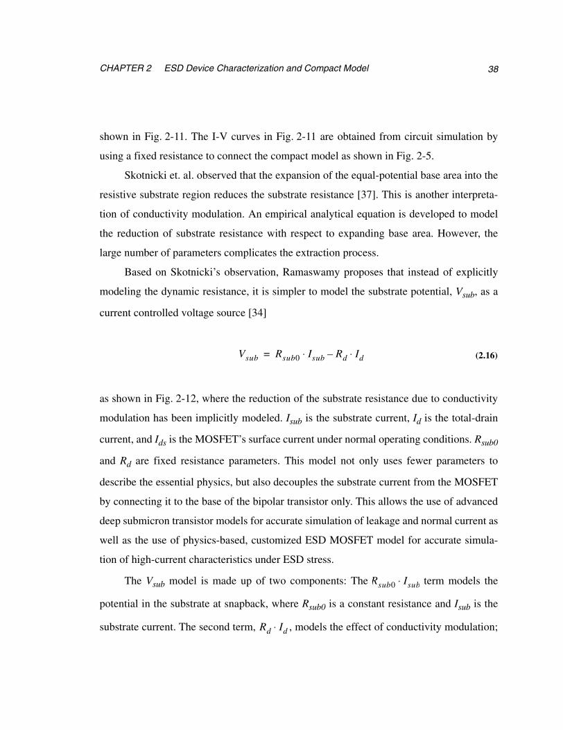
CHAPTER 2 ESD Device Characterization and Compact Model 38
shown in Fig. 2-11. The I-V curves in Fig. 2-11 are obtained from circuit simulation by
using a fixed resistance to connect the compact model as shown in Fig. 2-5.
Skotnicki et. al. observed that the expansion of the equal-potential base area into the
resistive substrate region reduces the substrate resistance [37]. This is another interpreta-
tion of conductivity modulation. An empirical analytical equation is developed to model
the reduction of substrate resistance with respect to expanding base area. However, the
large number of parameters complicates the extraction process.
Based on Skotnicki’s observation, Ramaswamy proposes that instead of explicitly
modeling the dynamic resistance, it is simpler to model the substrate potential, Vsub, as a
current controlled voltage source [34]
as shown in Fig. 2-12, where the reduction of the substrate resistance due to conductivity
modulation has been implicitly modeled. Isub is the substrate current, Id is the total-drain
current, and Ids is the MOSFET’s surface current under normal operating conditions. Rsub0
and Rd are fixed resistance parameters. This model not only uses fewer parameters to
describe the essential physics, but also decouples the substrate current from the MOSFET
by connecting it to the base of the bipolar transistor only. This allows the use of advanced
deep submicron transistor models for accurate simulation of leakage and normal current as
well as the use of physics-based, customized ESD MOSFET model for accurate simula-
tion of high-current characteristics under ESD stress.
The Vsub model is made up of two components: The term models the
potential in the substrate at snapback, where Rsub0 is a constant resistance and Isub is the
substrate current. The second term, , models the effect of conductivity modulation;
Vsub Rsub0 Isub⋅ Rd Id⋅–= (2.16)
Rsub0 Isub⋅
Rd Id⋅
392.6 Substrate Resistance Model
I d (
A)
ln (
I sub
(A
))
Vd (V)
Vg=1.5V
Vg=0.9V
Vg=1.5V
Vg=0.9V
experimental data
simulation results
FIGURE 2-11 The ESD I-V curve (solid line) is obtained using a constant
substrate resistance ( ) without considering conductivity
modulation. The discrepancy between the simulated Isub results and theexperimental data (circle) is significant.
Vsub Rsub0 Isub⋅=
CHAPTER 2 ESD Device Characterization and Compact Model 40
it only becomes significant after snapback. Rd models the drain resistance, including the
contact and spreading resistance in the drain junction; Id is the total drain current.
It was found that Ramaswamy’s substrate resistance model only shows good agree-
ment with experimental data over limited range of technology, namely the silicided tech-
nology, when implemented along with M and β [61,64]. Mismatch between the
experimental data and simulation results increases when the technology is changed from
silicided to nonsilicided. The silicided technology has emerged as the default for deep sub-
micron technology because the silicidation process lowers the source/drain resistance,
allowing for increased current drive capability and reduced output impendance. However,
Vsub
Substrate
Rsub+
-
FIGURE 2-12 The dynamic substrate resistance is modeled using a current-controlledvoltage source, Vsub. This compact model will be used to simulate the ESD protection
device.
Igen(M)Vsub
Id
IdsSource Drain
Gate
Ib
Isub
Icβrs rd
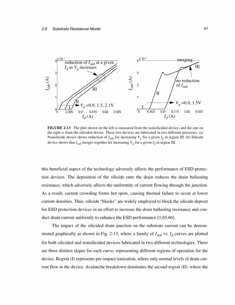
412.6 Substrate Resistance Model
this beneficial aspect of the technology adversely affects the performance of ESD protec-
tion devices. The deposition of the silicide onto the drain reduces the drain ballasting
resistance, which adversely affects the uniformity of current flowing through the junction.
As a result, current crowding forms hot spots, causing thermal failure to occur at lower
current densities. Thus, silicide “blocks” are widely employed to block the silicide deposit
for ESD protection devices in an effort to increase the drain ballasting resistance and con-
duct drain current uniformly to enhance the ESD performance [1,65,66].
The impact of the silicided drain junction on the substrate current can be demon-
strated graphically as shown in Fig. 2-13, where a family of Isub vs. Id curves are plotted
for both silicided and nonsilicided devices fabricated in two different technologies. There
are three distinct slopes for each curve, representing different regions of operation for the
device. Region (I) represents pre-impact ionization, where only normal levels of drain cur-
rent flow in the device. Avalanche breakdown dominates the second region (II), where the
Id (A) Id (A)
I sub
(A)
I sub
(A)
Vg =0.9, 1.5, 2.1V
reduction of Isub at a given Id as Vg increases
Vg =0.9, 1.5V
no reduction of Isub
FIGURE 2-13 The plot shown on the left is measured from the nonsilicided device, and the one onthe right is from the silicided device. These two devices are fabricated in two different processes. (a)Nonsilicide device shows reduction of Isub for increasing Vg for a given Id in region III. (b) Silicidedevice shows that Isub merges together for increasing Vg for a given Id in region III.
III
III I
III
II
merging
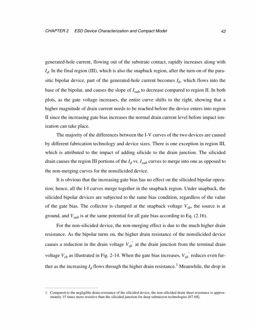
CHAPTER 2 ESD Device Characterization and Compact Model 42
generated-hole current, flowing out of the substrate contact, rapidly increases along with
Id. In the final region (III), which is also the snapback region, after the turn-on of the para-
sitic bipolar device, part of the generated-hole current becomes Ib, which flows into the
base of the bipolar, and causes the slope of Isub to decrease compared to region II. In both
plots, as the gate voltage increases, the entire curve shifts to the right, showing that a
higher magnitude of drain current needs to be reached before the device enters into region
II since the increasing gate bias increases the normal drain current level before impact ion-
ization can take place.
The majority of the differences between the I-V curves of the two devices are caused
by different fabrication technology and device sizes. There is one exception in region III,
which is attributed to the impact of adding silicide to the drain junction. The silicided
drain causes the region III portions of the Id vs. Isub curves to merge into one as opposed to
the non-merging curves for the nonsilicided device.
It is obvious that the increasing gate bias has no effect on the silicided bipolar opera-
tion; hence, all the I-I curves merge together in the snapback region. Under snapback, the
silicided bipolar devices are subjected to the same bias condition, regardless of the value
of the gate bias. The collector is clamped at the snapback voltage Vsb, the source is at
ground, and Vsub is at the same potential for all gate bias according to Eq. (2.16).
For the non-silicided device, the non-merging effect is due to the much higher drain
resistance. As the bipolar turns on, the higher drain resistance of the nonsilicided device
causes a reduction in the drain voltage Vsb’ at the drain junction from the terminal drain
voltage Vsb as illustrated in Fig. 2-14. When the gate bias increases, Vsb’ reduces even fur-
ther as the increasing Id flows through the higher drain resistance.1 Meanwhile, the drop in
1. Compared to the negligible drain resistance of the silicided device, the non-silicided drain sheet resistance is approx-imately 15 times more resistive than the silicided junction for deep submicron technologies [67-68].
432.6 Substrate Resistance Model
the collector voltage (Vsb’) brings about a decrease in the collector current so that the addi-
tional hole current has to flow to the base in order to maintain the same level of emitter
current. All of the above effects contribute to a decrease in the Isub curves as gate bias
increases at the fixed drain current level in the snapback region. Therefore, the Isub-Id
curves are not merged in region III for increasing gate bias. Although the Rd parameter
models the higher drain resistance, it is applied to all gate voltages; hence, the non-merg-
ing effect in region III of the nonsilicided device is not modeled by the Ramaswmay sub-
strate resistance model [61,64].
Instead of constructing another substrate model to simulate the effect of nonsilicided
device, the Ramaswamy model was modified to include the effects of the drain resistance,
which are manifest in the reduction of the Isub as the gate voltage increases during the
snapback. For modeling purposes, the effects can be interpreted as the “early” turn-on of
the bipolar device at a lower Isub. Thus, the proposed solution is to add the term to
Vsb
Vsb’
drain resistance
FIGURE 2-14 Reduction of Vsb to Vsb’ after the potential drop occurs on the large
drain resistance for the nonsilicided block. As Vg increases, Ids increases, dropping
more voltage across the drain resistance, reducing Vsb’ further and decreasing the
magnitude of Isub.
Rd Ids⋅
CHAPTER 2 ESD Device Characterization and Compact Model 44
the substrate resistance model to simulate the “early” turn-on of the bipolar with respect to
the increasing gate bias observed in nonsilicided device [64]
The product is negligible for silicided drain device because of the small values of
Rd. But it is significant for the non-silicided device; the product increases as the gate volt-
age, turning on the bipolar at a lower Isub value. More general in scope, the modified sub-
strate resistance model can simulate both silicided and nonsilicided devices accurately.
2.7 EXTRACTION OF Rsub PARAMETERS
As in Eq. (2.17), the dynamic substrate resistance is modeled as a current controlled
voltage source, Vsub; the extraction of Vsub parameters is relatively straightforward com-
paring to M. Rsub0 and Rd are circuit model parameters that can be extracted from the
snapback portion of the Isub vs. Id data as illustrated in Fig. 2-15 [34]. A straight line is
curve fitted to the snapback portion of the experimental data,
Rsub0, which represents the bulk resistance at the on-set of snapback, was extracted using
the y-intercept
Vsub Rsub0 Isub⋅ Rd Id Ids–( )⋅–= (2.17)
Rd Ids⋅
Isub
Isub∆Id∆
------------ Id⋅ Isub0+= (2.18)
Rsub0
Vbeon
Isub0-------------= (2.19)

452.7 Extraction of Rsub Parameters
where Vbeon is the turn-on voltage (typically 0.7-0.8V) of the base-emitter junction of the
parasitic bipolar transistor for deep submicron MOS, Isub0 is the y-intercept. Rd models the
conductivity modulation by relating the substrate current (Isub) to the total drain current
(Id); Rd is extracted from the slope of the line and Rsub0
Isub0 slope
Isub
Isub∆Id∆
------------ Id⋅ Isub0+=
Id (A)
I sub
(A
)
FIGURE 2-15 A straight line is fitted to the snapback region of the Id vs. Isub plot. Rsub0 and
Rd can be extracted from the linear equation.
Rd
Isub∆Id∆
------------ Rsub0⋅= (2.20)
CHAPTER 2 ESD Device Characterization and Compact Model 46
where is the slope.
The Rsub0 and Rd for the 0.35µm device are listed in Table 2-2 along with the
extracted bipolar parameters in section 2.9.
2.8 PARASITIC BIPOLAR TRANSISTOR MODELING
The impact ionization and growth in substrate potential are all preludes to the main
ESD operation, the snapback action. Snapback is an important mechanism for switching
the protection device from a high-to low-impedance state essential for efficient discharge
of the ESD current. As the parasitic bipolar device turns on, Id rapidly increases due to the
additional collector current; hence, M can decrease and still maintain the hole generation
current required to sustain the bipolar action according to Eq. (2.1) and Eq. (2.4). The
snapback holding voltage, Vsb, is defined as occurring when [29,35]
which is also the condition for positive feedback of the circuit in Fig. 2-12. In this equa-
tion, β is the current gain of the bipolar device, and M is the avalanche multiplication fac-
tor. The above expression can be obtained by solving for the emitter current, Ie, in terms of
all the other circuit parameters, and then setting the denominator of Ie to zero.
Extensive work has been done to model the bipolar transistor under avalanche condi-
tions for circuit simulation [69-71]. Diaz, extending the work further, used the Gummel-
Poon (GP) model to simulate the lateral parasitic bipolar device [72]. The relative large
number of parameters in the GP model complicates the extraction process and increases
the number of required measurements [8].
Isub∆Id∆
------------
β M 1–( )⋅ 1≥ (2.21)

472.8 Parasitic Bipolar Transistor Modeling
In addition, Amerasekera et. al. pointed out that there are fundamental differences
between the parasitic and lateral bipolar devices; therefore, the lateral bipolar model can-
not accurately simulate the parasitic bipolar action [29]. The two types of bipolar devices
differ in terms of the active emitter/collector area and the base bias method. The emitter
and collector of the parasitic bipolar are formed only by the sidewall portions of the LDD
source and drain junctions. The side walls have the depth of the LDD junction and the
width of the device. By comparison, the lateral bipolar has much wider emitter and collec-
tor areas, which not only include all of the LDD junction areas but also the n+ source/drain
junction areas. Moreover, the parasitic device generates hole current from impact ioniza-
tion, establishing its base potential for self-bias; it also maintains the base current from the
generated hole current, unlike the lateral bipolar device that obtains Vbe bias and Ib from
an external source. As a result, the source/drain areas that do not function as the emitter/
collector and the self-bias mechanism will influence the measurement and extraction of
parameters such as β and contact resistance.
Based on the above observations, Amerasekera et. al. formulated a simpler bipolar
model because the large number of parameters associated with the GP model becomes
unnecessary when the parasitic bipolar operates under almost fixed bias conditions under
the snapback. Obviously, β is the key parameter to model for the bipolar device; it is
defined as [48]
where Ib is the base current and Ic is the collector current.
βIc
Ib----≡ (2.22)
CHAPTER 2 ESD Device Characterization and Compact Model 48
The expression for Ib and Ic can be found from the basic bipolar model [48]. Due to
the reverse bias between the base-collector junction, Ic can be simplified as
The base current is described as
where Ioe is the reverse saturation current due to diffusion of holes, Ioc is the transport cur-
rent, the thermal voltage, is the Boltzmann’s constant, and Vbe is the base-emit-
ter voltage. For a npn transistor, a simplified form for Ioc is defined as
where ni is the intrinsic concentration, AE is the effective emitter area of the parasitic tran-
sistor, Dn is the effective diffusion constant for electrons, NB is the doping in the base, and
WB is the base width. Typically, AE is the sidewall LDD junction area, defined as
; Dn is determined by the Einstein relationship, defined as Dn= , and
WB is the effective channel length.
Similarly, Ioe is given by
Ic Ioc
Vbe
VT--------exp= (2.23)
Ib Ioe
Vbe
VT-------- 1–exp= (2.24)
VTKTq
-------=
Ioc
qni2AEDn
NBWB------------------------= (2.25)
AE χj W⋅= VT µn⋅
Ioe
q ni2
AE Dp⋅ ⋅ ⋅NE LpE⋅
------------------------------------= (2.26)
492.9 EXTRACTION OF b
where Dp is the effective diffusion constant for holes in the emitter, NE is the emitter con-
centration, and LpE is the hole diffusion length. According to Eq. (2.22), β can be written
as
The magnitudes of Ioc and Ioe depend mainly on the processing conditions, accord-
ing to Eq. (2.25). Ioc only varies with two layout parameters: the channel length, also
known as the base width for the parasitic bipolar, and the active emitter area; Ioe is only
sensitive to the emitter area. Based on Eq. (2.27), β depends on the base width.
2.9 EXTRACTION OF β
The bipolar model parameters Ioc and Ioe need to be extracted from the snapback
data in order to determine β. However, for the Ioc extraction in the snapback region, it
becomes difficult to isolate the collector current from the generated hole current. We uti-
lize the extracted M and Rsub0 values to distinguish the collector current to solve for Ioc
and Ioe. Combining Eqs. (2.1) and (2.4), putting Igen in terms of and M, the collec-
tor current can be solved for as [29]
where Ids is the normal MOS current that can be obtained from the measurements. Substi-
tuting this expression for Ic into Eq. (2.23) as well as Vsub expression for Vbe in the same
βIoc
Ioe------= (2.27)
Ic Ids+
Ic
Id
M----- Ids–= (2.28)
CHAPTER 2 ESD Device Characterization and Compact Model 50
equation, Ioc can be described as [29]
Vsub is the substrate voltage described in the earlier section. It is a function of the substrate
resistance and substrate current.
Using Eqs. (2.28), (2.1), and (2.2), putting Igen in terms of Id and M, the base current
can be expressed as [29]
Combining Eqs. (2.22), (2.28), and (2.30), in terms of currents that can be experi-
mentally measured (Id, Ids and Isub), β can be written as
Ioc
Id
M----- Ids–
Vsub
VT----------exp
--------------------------= (2.29)
Ib
Id M 1–( )M
----------------------- Isub–= (2.30)
β
Id
M----- Ids–
Id M 1–( )⋅M
--------------------------- Isub–
-------------------------------------------= (2.31)

512.10 High Current ESD Compact Model Implementation
From Eqs. (2.29) and (2.31), Ioc and Ioe can be extracted from a specific M and Vsub
data point in the snapback portion of the I-V curve. Once extracted, they can be used to
fine-tune the simulated high I-V curves to measured data.
The extracted Ioc and Ioe parameters for the 0.35µm device are listed in Table 2-2.
Unlike the M parameters, the Rsub and β parameters are highly sensitive to the geometry of
the device; this layout dependency of Rsub and β will be analyzed and modeled in detail in
the following chapter.
Thus far, all the critical parameters M, Rsub and β have been modeled and extracted.
2.10 HIGH CURRENT ESD COMPACT MODEL
IMPLEMENTATION
The high-current compact model has been constructed and extraction of the key
model parameters have been discussed. This compact model needs to be implemented into
a circuit simulator for high current I-V simulation. This compact model is implemented as
a subcircuit in the commercial circuit simulator, HSPICE. HSPICE is used broadly in
industry; hence, the subcircuit implementation method offers portability and simplicity.
The subcircuit configuration is shown in Fig. 2-12. The normal nMOS operation is
simulated using the BSIM transistor model. The basic BJT model described in the previ-
ous section is used to model the parasitic BJT action in the snapback region. The substrate
resistance model Vsub is also implemented. The generation current source, Igen, is modeled
as a sum of two current-controlled-current sources. One is controlled by Ic and M; the
Extracted Rsub Parameters Extracted BJT Parameters
Rsub0 (Ω) Rd (Ω) Ioc (Α) Ioe (Α) β
2960 415 6e-18 1e-18 6
TABLE 2-2 Rsub and BJT parameters for the 0.35µm device
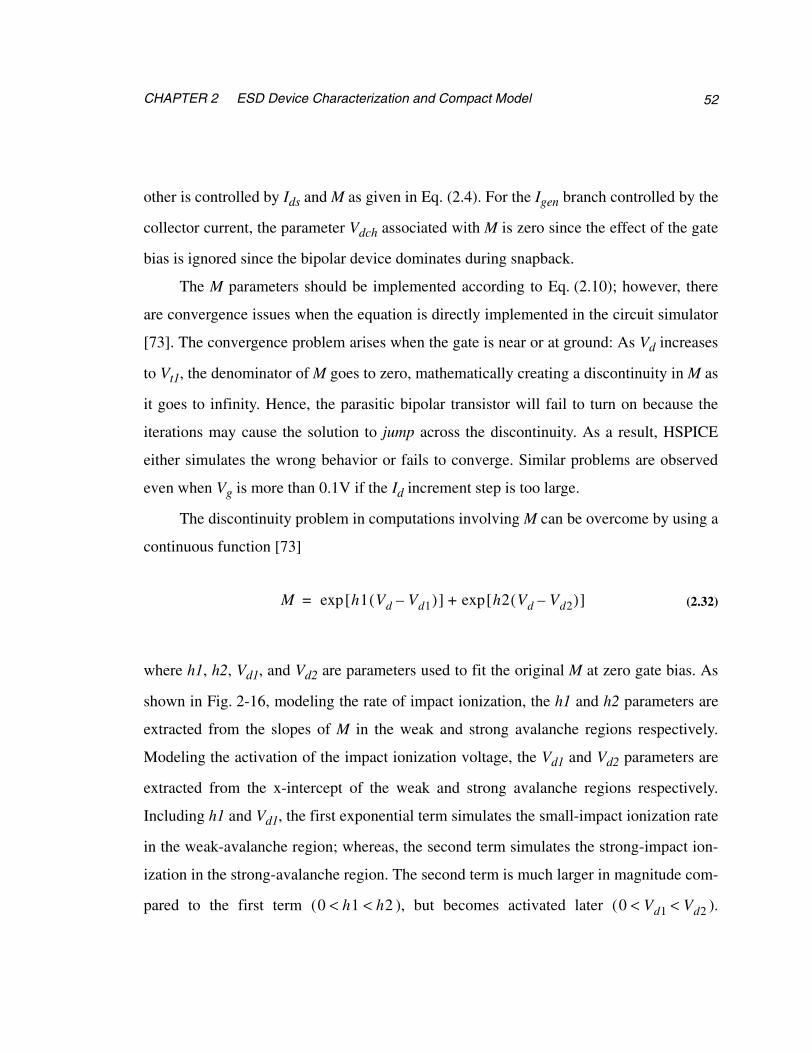
CHAPTER 2 ESD Device Characterization and Compact Model 52
other is controlled by Ids and M as given in Eq. (2.4). For the Igen branch controlled by the
collector current, the parameter Vdch associated with M is zero since the effect of the gate
bias is ignored since the bipolar device dominates during snapback.
The M parameters should be implemented according to Eq. (2.10); however, there
are convergence issues when the equation is directly implemented in the circuit simulator
[73]. The convergence problem arises when the gate is near or at ground: As Vd increases
to Vt1, the denominator of M goes to zero, mathematically creating a discontinuity in M as
it goes to infinity. Hence, the parasitic bipolar transistor will fail to turn on because the
iterations may cause the solution to jump across the discontinuity. As a result, HSPICE
either simulates the wrong behavior or fails to converge. Similar problems are observed
even when Vg is more than 0.1V if the Id increment step is too large.
The discontinuity problem in computations involving M can be overcome by using a
continuous function [73]
where h1, h2, Vd1, and Vd2 are parameters used to fit the original M at zero gate bias. As
shown in Fig. 2-16, modeling the rate of impact ionization, the h1 and h2 parameters are
extracted from the slopes of M in the weak and strong avalanche regions respectively.
Modeling the activation of the impact ionization voltage, the Vd1 and Vd2 parameters are
extracted from the x-intercept of the weak and strong avalanche regions respectively.
Including h1 and Vd1, the first exponential term simulates the small-impact ionization rate
in the weak-avalanche region; whereas, the second term simulates the strong-impact ion-
ization in the strong-avalanche region. The second term is much larger in magnitude com-
pared to the first term ( ), but becomes activated later ( ).
M h1 Vd Vd1–( )[ ]exp h2 Vd Vd2–( )[ ]exp+= (2.32)
0 h1 h2< < 0 Vd1 Vd2< <

532.10 High Current ESD Compact Model Implementation
Together the two exponential terms are designed to model the original M from the weak to
strong avalanche, resulting in a smooth I-V transition from the off state to the junction
breakdown. Since this formulation simulates the correct I-V behavior at , it can be
directly implemented in a HSPICE subcircuit in addition to the original M model.
After completing the M, Rsub, and BJT implementation in HSPICE, the transistor is
simulated under high-current stress, the simulation results are compared against the exper-
imental data in Fig. 2-17 and Fig. 2-18. The circuit model accurately simulates the high-
Vd1Vd2
slope h2
slope h1
Vd (V)
lnM
at V
g0
=
FIGURE 2-16 The two solid lines, whose slopes are fitted to the original Mcurve (solid curve), are used to extract the Vd1, h1, Vd2, and h2 for the
continuous M formulation. Vd1, h1, Vd2, and h2 are extracted to be 3.9V, 0.14V-
1, 11V, 66.67V-1 respectively.
Vg 0=
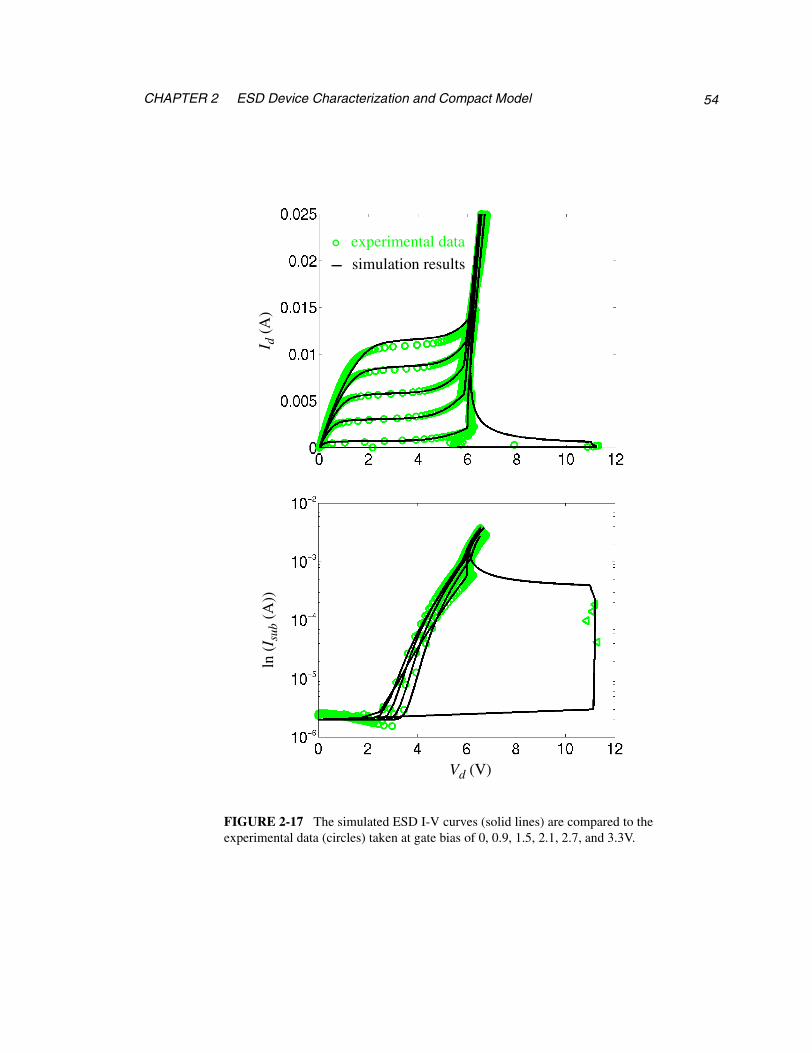
CHAPTER 2 ESD Device Characterization and Compact Model 54
I d (
A)
ln (
I sub
(A
))
Vd (V)
experimental data
simulation results
FIGURE 2-17 The simulated ESD I-V curves (solid lines) are compared to theexperimental data (circles) taken at gate bias of 0, 0.9, 1.5, 2.1, 2.7, and 3.3V.
552.11 Impacts of Scaling
current behavior under the ESD stress; in addition, the correct results are achieved at
using the continuous M function.
2.11 IMPACTS OF SCALING
The previous sections discussed the modeling and parameter extraction processes for
the impact ionization factor M, substrate resistance Rsub, and current gain β of the MOS-
FET transistor. In this section, the impact of technology and geometry scaling on M, β,
and Rsub are examined as reflected by the trends in the Vsb, Vt1, and It1. Based on the
trends, the scaling effects can incorporated into the compact model to accurately model
the geometric and technological variations.
Vg 0=
I sub
(A
)
Id (A)
experimental data
simulation results
FIGURE 2-18 The simulated Isub vs. Id (solid line) is compared to the
experimental data (circles) at gate bias of 0, 0.9, 1.5, 2.1, 2.7, and 3.3V.
CHAPTER 2 ESD Device Characterization and Compact Model 56
For robust ESD performance, Vt1 and Vsb needs to be small in order to reduce the
voltage stress on the pin; It1, the trigger current, also needs to be low so that the thermal
heating occurs later in the breakdown process. To accomplish the above conditions, the
magnitudes of M, Rsub, and β have to be large. A large M implies a high rate of impact ion-
ization, resulting in a smaller Vt1. Similarly, a high β means more current gain, yielding a
lower Vsb. A large Rsub can turn the bipolar on at a lower substrate current, resulting in a
lower It1 current [1].
As technology scales down to 0.1µm and beyond, the drain, the substrate, and the
channel continue to be scaled aggressively to improve normal current drive capabilities
while still maintaining gate control and low leakage current. The changes in the process-
ing technology can greatly change the process dependence of M as well; changes in the
device geometry can significantly alter the substrate resistance and β. As a result, the
high-current characteristics of a ESD protection device will change accordingly to the spe-
cific technology and geometry.
Deep submicron process design concentrates on the drain and channel region. Drain
and channel engineering, which include the design of the LDD junction and the channel
doping1, are essential to reduce hot carriers effects and maintain gate control during nor-
mal operation. As the feature size shrinks, the channel doping concentration is scaled up in
an effort to maintain threshold voltage control; moreover, the pocket implant−an implant
with higher doping than the channel−is implanted around the drain and source junctions to
prevent punch through. In order to lower the rising electric field associated with the
increasing channel doping, the LDD junction has to become shallower. The shallower and
graded LDD junction reduces the rate of the impact ionization; therefore, M should
decrease as scaling continues. Yet, more than compensating for the reduction in M, the
higher channel doping level increases the carriers available for the hole generation; hence,
1. In this context, the channel doping refers to threshold adjust implants, punch-through implants, etc.
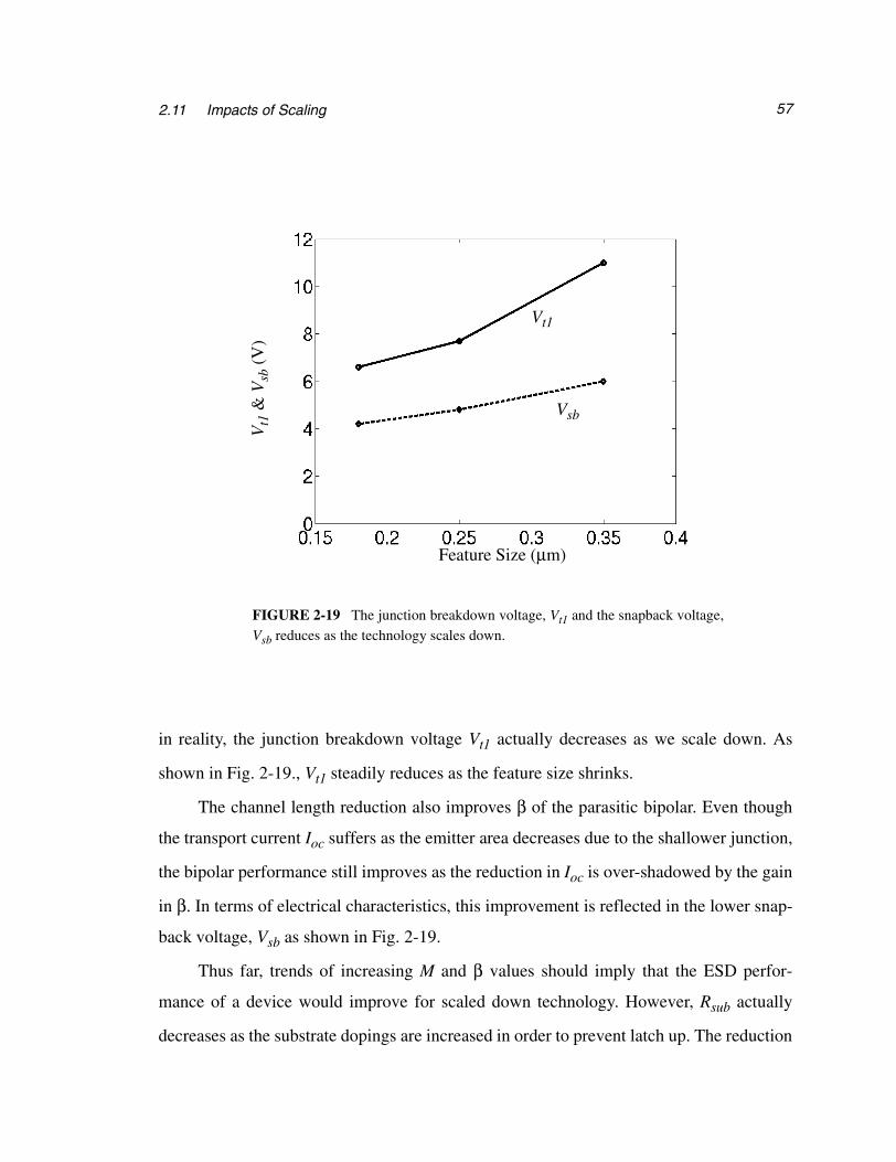
572.11 Impacts of Scaling
in reality, the junction breakdown voltage Vt1 actually decreases as we scale down. As
shown in Fig. 2-19., Vt1 steadily reduces as the feature size shrinks.
The channel length reduction also improves β of the parasitic bipolar. Even though
the transport current Ioc suffers as the emitter area decreases due to the shallower junction,
the bipolar performance still improves as the reduction in Ioc is over-shadowed by the gain
in β. In terms of electrical characteristics, this improvement is reflected in the lower snap-
back voltage, Vsb as shown in Fig. 2-19.
Thus far, trends of increasing M and β values should imply that the ESD perfor-
mance of a device would improve for scaled down technology. However, Rsub actually
decreases as the substrate dopings are increased in order to prevent latch up. The reduction
Feature Size (µm)
Vt1
& V
sb (
V)
FIGURE 2-19 The junction breakdown voltage, Vt1 and the snapback voltage,Vsb reduces as the technology scales down.
Vsb
Vt1

CHAPTER 2 ESD Device Characterization and Compact Model 58
of Rsub raises the amount of substrate current needed to turn on the parasitic bipolar; the
high-substrate current can then heat up the device at a lower total current, leading to a
smaller It2 value, and degrading the overall ESD performance of the device.
Fig. 2-20 illustrates the high-current characteristics of two devices which were fabri-
cated in two different technologies, 0.35µm and 0.25µm. As discussed above, Vt1 and Vsb
are lower for the 0.25µm technology device; on the other hand, Isub at the snapback
increases due to Rsub reduction for the same technology. This example demonstrates that
Id (A)
FIGURE 2-20 The y-axis intercept of the 0.35µm device (solid line, fabricated inthe 0.35µm technology) is lower than the y-intercept of the 0.25µm device (dashedline, fabricated in the 0.25µm technology), demonstrating a lower Rsub0 value for the0.25µm device.
0.35µm device
0.25µm device
592.11 Impacts of Scaling
the substrate resistance is the key element that affects the ESD performance of a device in
technology scaling; therefore, it must be modeled accurately.
In the following chapters, the placement of the substrate contacts or the length of the
channel will be shown to affect the substrate resistance value. The substrate model pre-
sented in this chapter cannot calculate the resistance value according to the different lay-
outs. Hence, the current Rsub model will be modified to simulate layout variations for any
given technology.

CHAPTER 2 ESD Device Characterization and Compact Model 60

CHAPTER 3
THE SUBSTRATE RESISTANCE MODEL: THE QUASI-MIXED-MODE METHODOLOGY
3.1 RSUB MODEL BACKGROUND
During electro-static discharge, the magnitude of the substrate resistance, Rsub,
determines the on/off state of the parasitic bipolar transistor that forms a current path from
drain to source and substrate. More importantly, the interactions of different circuit ele-
ments through the common substrate can have a significant impact on the circuit’s ESD
performance. Especially as the technology continues to scale down, concurrently trying to
suppress short-channel effects and reduce noise coupling through the substrate, process
steps such as the addition of retrograde substrate doping, threshold adjust implants, pocket
implants, and p-epi layers (p- region), all result in a net increase of the substrate doping,
causing a reduction in substrate resistance. Smaller substrate resistance degrades ESD per-
formance since more substrate current is needed to turn on the parasitic bipolar transistor,
60

CHAPTER 3 The Substrate Resistance Model: The Quasi-Mixed-Mode Methodology 61
resulting in device heating at an earlier stage, and thus, leading to a second breakdown for
lower drain current levels. Therefore, precise modeling of the substrate resistance that
captures effects of layout and fabrication process is needed in order to perform accurate
circuit level ESD simulation. Moreover, the fact that the substrate resistance is conductiv-
ity modulated during ESD event also needs to be included in order to accurately simulate
the substrate current [37]. The injection of minority carriers into the base after the turn-on
of the parasitic bipolar causes conductivity modulation.
The effects of conductivity modulation can be seen from the experimental data,
which shows that the substrate current continues to increase after snapback; hence, to
maintain a constant base voltage for the parasitic BJT, the substrate resistance must
decrease. Instead of explicitly modeling the dynamic substrate resistance, the substrate
potential is modeled as a current controlled voltage source [34,64,74]
where Isub is the substrate current, Id is the total drain current, and Ids is the MOSFET’s
surface current under normal operating conditions. Rsub0 and Rd are constant resistance
parameters that model the physical substrate resistance and the conductivity modulated
resistance respectively. Their values are strongly affected by the layout of the protection
transistor.
When designing an ESD protection transistor, there are many geometric variations to
be considered, including: the placement of substrate contact, length of the channel, and
drain contact to gate spacing−all of which affect the magnitude of substrate resistance.
However, the compact model presented thus far lacks the layout dependent modeling
capability, because extracted Rsub0 and Rd are fixed and hence fail to predict the effects of
layout and process variations. Therefore, these resistors must be extracted again from the
experimental data for each different layout and technology; unlike, the impact ionization
Vsub Rsub0 Isub⋅ Rd Id Ids–( )⋅–= (3.1)

623.1 Rsub Model Background
M parameters described in the previous chapter which primarily depends on technology.
The inability of the compact model parameters to scale with device geometry is a major
drawback; therefore, the substrate resistance model needs to be extended to account for
the layout variations [74].
Analytical formula have been developed to calculate the magnitude of substrate resis-
tance, namely the Rsub0 parameter. Assuming that the hole current flows into the substrate
uniformly and the substrate doping is constant, Hu et. al. demonstrated that the substrate
resistance can be expressed analytically to account for the channel length variation of a
nMOS for an artificially placed substrate contact (on the bottom of the device) [35]. Since
the analysis did not take into account the non-uniform substrate doping and hence the
dopant dependent hole current distribution inside the substrate for deep submicron tech-
nologies, the substrate resistance expression cannot be quantitatively accurate. Extensive
calibrations can be performed based on the actual structures to empirically fit the experi-
mental resistance, but this approach does not improve the compact model. More impor-
tantly, the Rsub0 expression assumes that the substrate contact is artificially located along
the bottom of the device. Therefore, any changes in the placement of substrate contacts
along the surface of the device require re-calibration, thus, changing the parameters of the
analytical Rsub0 expression.
Other approaches employ substrate resistance networks to simulate the effects of dif-
ferent layouts [38,75-79]. Without accounting for conductivity modulation, these models
overestimate the substrate resistance and in turn underestimate the substrate current, as
shown in Fig. 3-1, and therefore lead to inaccurate values for the second breakdown [73-
74]. Li et. al’s network included the conductivity modulation effect, but extensive calibra-
tions are required to accurately divide the conductivity modulated substrate area from that
of the pure substrate resistance region [38]. Ramaswamy et. al. generate the entire Rsub0
network based on the substrate doping; they then account for modulation effects by selec-
tively modifying the appropriate resistances in the network [79]. Again extensive calibra-

CHAPTER 3 The Substrate Resistance Model: The Quasi-Mixed-Mode Methodology 63
I d (
A)
ln (
I sub
(A
))
Vd (V)
Vg=1.5V
Vg=0.9V
Vg=1.5V
Vg=0.9V
experimental data
simulation results
FIGURE 3-1 The ESD I-V curve (solid line) is obtained using a constant
substrate resistance ( ) without considering conductivity
modulation. The discrepancy between the simulated Isub results and theexperimental data (circle) is significant. Note: this is the same as Fig. 2-11. It isplotted again for easy reference.
Vsub Rsub0 Isub⋅=
643.1 Rsub Model Background
tion based on the real devices is needed to determine the individual resistances that are
affected by conductivity modulation in the network. Although these methods offer more
insight into the scaling of the substrate resistance with respect to layout geometries, a clear
picture of the interplay between substrate resistance and the parasitic bipolar device is still
missing on the physical level.
After careful calibration, device simulators that construct a virtual two-dimensional
cross-section for the device can simulate both the change of substrate resistance due to the
ESD stress and layout variations. However, the computation of impact ionization and the
snapback portions of the ESD I-V curve often cause convergence problems and can
become computationally too expensive, even for a single device. Moreover, these prob-
lems are compounded by the large size of the ESD protection device which results from
the actual placement of substrate contacts on the top of the device (as opposed to placing it
on the bottom). It becomes unstable and inefficient to use pure device simulator as an
effective tool for design of experiments that involve the simulation of many devices [4].
Hence, it is desirable to formulate a methodology that can account for conductivity modu-
lation, process, and layout variations in the substrate resistance modeling to allow for
improved circuit simulation capabilities.
This dissertation aims to extend the capability of the current-controlled substrate
potential model (Vsub model) using a novel method called the Quasi-Mixed-Mode (QMM)
approach so that the Rsub0 and Rd parameters can be simulated for different layouts and
technologies based on a few calibrated devices, instead of directly extracting the resistor
values from experimental data. This approach helps to model the substrate resistance more
accurately, as a function of the layout and process, and enables circuit designers to identify
the critical current paths during the ESD stress and to design an effective protection device
based on the layout [74].
CHAPTER 3 The Substrate Resistance Model: The Quasi-Mixed-Mode Methodology 65
3.2 THE QMM APPROACH
The Quasi-Mixed-Mode modeling approach is a marriage between device and cir-
cuit simulations. The model differs from the traditional mixed-mode (device/circuit) simu-
lation because it does not use a fully coupled matrix approach, which can be
computationally expensive. Furthermore, the traditional mixed-mode approach only sup-
ports the simulation using a voltage ramp and does not have built-in curve tracer simula-
tion control for the snapback action, making it less user-friendly. For the QMM method,
the two simulators are coupled indirectly; only the results of the device simulation are fed
into the circuit model, hence the adjective quasi (as opposed to fully- or tightly-coupled) is
used.
The Quasi-Mixed-Mode methodology uses either the circuit or device simulator to
model the lumped and distributed circuit elements, respectively. As discussed in Chapter 2
and as shown in Fig. 3-2, for a given technology, the process-dependent parameters, such
as M, do not vary once extracted, so the physical effects can be modeled as lumped ele-
ments. Therefore, the impact ionization model (M factor) parameters are implemented
directly in the compact model along with the parameters that govern the normal MOSFET
operation. On the other hand, β depends in part on the channel length, while the substrate
resistance parameters depend on the layout; therefore, they are better suited for use in a
distributed-element model. The device simulator computes the substrate resistance based
on the layout. The compact model uses the simulated substrate resistance and in turn sim-
ulates the resulting overall ESD I-V curve.
The QMM was developed with the purpose of modeling substrate resistance for the
protection device. Hence it is much faster, more robust, and easier to calibrate compared to
the full device simulation. In addition, the substrate resistance parameters are able to
account for layout and process variations which extend the capabilities of the circuit
model. Hence, the Quasi-Mixed-Mode model can be used as an effective tool in designing
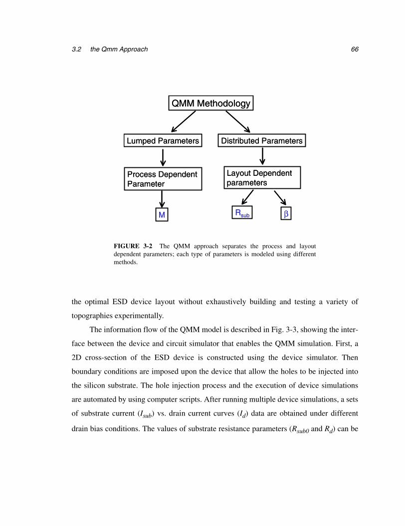
663.2 the Qmm Approach
the optimal ESD device layout without exhaustively building and testing a variety of
topographies experimentally.
The information flow of the QMM model is described in Fig. 3-3, showing the inter-
face between the device and circuit simulator that enables the QMM simulation. First, a
2D cross-section of the ESD device is constructed using the device simulator. Then
boundary conditions are imposed upon the device that allow the holes to be injected into
the silicon substrate. The hole injection process and the execution of device simulations
are automated by using computer scripts. After running multiple device simulations, a sets
of substrate current (Isub) vs. drain current curves (Id) data are obtained under different
drain bias conditions. The values of substrate resistance parameters (Rsub0 and Rd) can be
QMM Methodology
Lumped Parameters Distributed Parameters
Process Dependent Parameter
M
Layout Dependent parameters
Rsub β
QMM Methodology
Lumped Parameters Distributed Parameters
Process Dependent Parameter
M
Layout Dependent parameters
Rsub β
FIGURE 3-2 The QMM approach separates the process and layoutdependent parameters; each type of parameters is modeled using differentmethods.
CHAPTER 3 The Substrate Resistance Model: The Quasi-Mixed-Mode Methodology 67
extracted from these curves as a function of drain bias (Vd), and imported into the compact
model as [74]
for subsequent circuit level simulation. The compact model shown in Fig. 3-4 is imple-
mented as a macro model in the circuit simulator. The circuit parameters for normal MOS-
FET operation and impact ionization are already extracted from experimental data
according to the methodology described in Chapter 2.
The QMM methodology improves on the traditional approach using only device
simulation in terms of computational speed, robustness, and calibration steps by avoiding
the computational problems of using a full ESD event simulation at the device level. The
QMM method achieves the improvements by setting up the boundary conditions to bypass
the direct simulation of impact ionization; thus, the device simulation can be simplified to
predict the substrate resistance with stability and speed. Fig. 3-5 illustrates the placement
of boundary conditions on the ESD devices. The boundary placement is equivalent to arti-
ficially removing the nMOS device entirely by setting the gate bias to zero while simulat-
ing the bipolar transistor operation corresponding to that shown in Fig. 3-4. The gate,
source, and substrate contacts are all tied to the ground. Instead of ramping up the drain
terminal as in normal device simulation, this simulation has a fixed bias to establish the
corresponding electric field and depletion areas. Fixing the voltage bias on the drain of the
device is similar to the operating condition in the snapback region, where the drain voltage
is roughly constant while the currents change quite dramatically.
A localized Igen, introduced using photogeneration in the device simulator, is swept
until the parasitic bipolar turns on. The magnitude of Igen is controlled by injecting the
Vsub Rsub0 Vd( ) Isub⋅ Rd Vd( ) Id Ids–( )⋅–= (3.2)
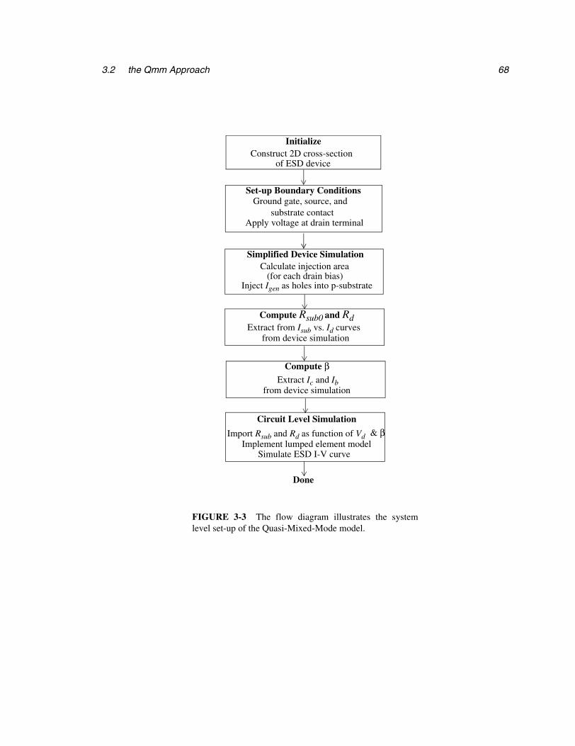
683.2 the Qmm Approach
Initialize
Ground gate, source, and Set-up Boundary Conditions
Simplified Device SimulationCalculate injection area
Inject Igen as holes into p-substrate
Compute Rsub0 and Rd
Done
Construct 2D cross-sectionof ESD device
Apply voltage at drain terminal
(for each drain bias)
Extract from Isub vs. Id curvesfrom device simulation
Circuit Level Simulation
Import Rsub and Rd as function of VdImplement lumped element model
Simulate ESD I-V curve
substrate contact
FIGURE 3-3 The flow diagram illustrates the systemlevel set-up of the Quasi-Mixed-Mode model.
Extract Ic and Ib from device simulation
Compute β
& β
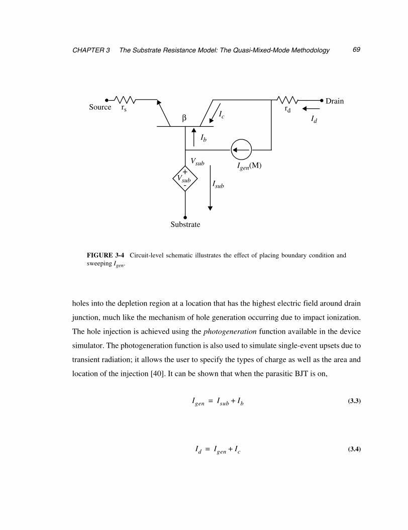
CHAPTER 3 The Substrate Resistance Model: The Quasi-Mixed-Mode Methodology 69
holes into the depletion region at a location that has the highest electric field around drain
junction, much like the mechanism of hole generation occurring due to impact ionization.
The hole injection is achieved using the photogeneration function available in the device
simulator. The photogeneration function is also used to simulate single-event upsets due to
transient radiation; it allows the user to specify the types of charge as well as the area and
location of the injection [40]. It can be shown that when the parasitic BJT is on,
Vsub
Substrate
+
-
Igen(M)Vsub
Id
SourceDrain
Ib
Isub
Icβrs rd
FIGURE 3-4 Circuit-level schematic illustrates the effect of placing boundary condition andsweeping Igen.
Igen Isub Ib+= (3.3)
Id Igen Ic+= (3.4)
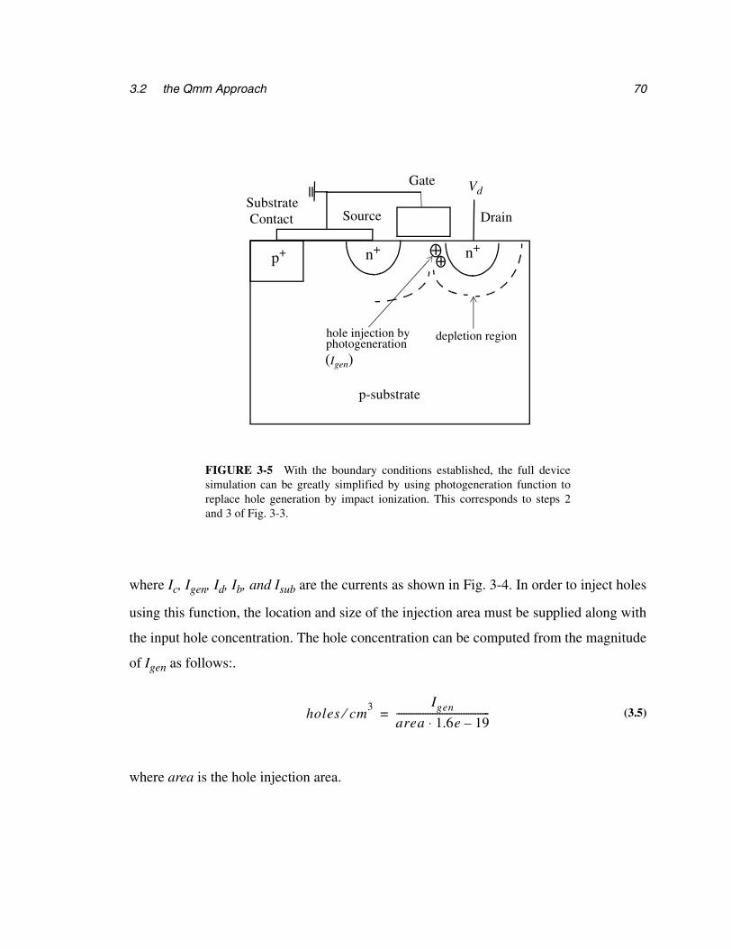
703.2 the Qmm Approach
where Ic, Igen, Id, Ib, and Isub are the currents as shown in Fig. 3-4. In order to inject holes
using this function, the location and size of the injection area must be supplied along with
the input hole concentration. The hole concentration can be computed from the magnitude
of Igen as follows:.
where area is the hole injection area.
Gate
Substrate
p-substrate
n+p+ n+
Source Drain
Vd
hole injection byphotogeneration
depletion region
Contact
(Igen)
FIGURE 3-5 With the boundary conditions established, the full devicesimulation can be greatly simplified by using photogeneration function toreplace hole generation by impact ionization. This corresponds to steps 2and 3 of Fig. 3-3.
holes cm3⁄
Igen
area 1.6e 19–⋅---------------------------------------= (3.5)
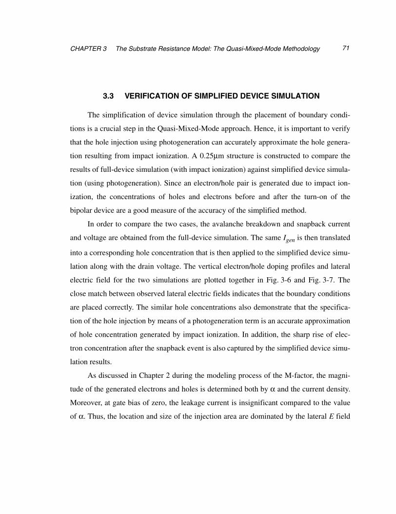
CHAPTER 3 The Substrate Resistance Model: The Quasi-Mixed-Mode Methodology 71
3.3 VERIFICATION OF SIMPLIFIED DEVICE SIMULATION
The simplification of device simulation through the placement of boundary condi-
tions is a crucial step in the Quasi-Mixed-Mode approach. Hence, it is important to verify
that the hole injection using photogeneration can accurately approximate the hole genera-
tion resulting from impact ionization. A 0.25µm structure is constructed to compare the
results of full-device simulation (with impact ionization) against simplified device simula-
tion (using photogeneration). Since an electron/hole pair is generated due to impact ion-
ization, the concentrations of holes and electrons before and after the turn-on of the
bipolar device are a good measure of the accuracy of the simplified method.
In order to compare the two cases, the avalanche breakdown and snapback current
and voltage are obtained from the full-device simulation. The same Igen is then translated
into a corresponding hole concentration that is then applied to the simplified device simu-
lation along with the drain voltage. The vertical electron/hole doping profiles and lateral
electric field for the two simulations are plotted together in Fig. 3-6 and Fig. 3-7. The
close match between observed lateral electric fields indicates that the boundary conditions
are placed correctly. The similar hole concentrations also demonstrate that the specifica-
tion of the hole injection by means of a photogeneration term is an accurate approximation
of hole concentration generated by impact ionization. In addition, the sharp rise of elec-
tron concentration after the snapback event is also captured by the simplified device simu-
lation results.
As discussed in Chapter 2 during the modeling process of the M-factor, the magni-
tude of the generated electrons and holes is determined both by α and the current density.
Moreover, at gate bias of zero, the leakage current is insignificant compared to the value
of α. Thus, the location and size of the injection area are dominated by the lateral E field
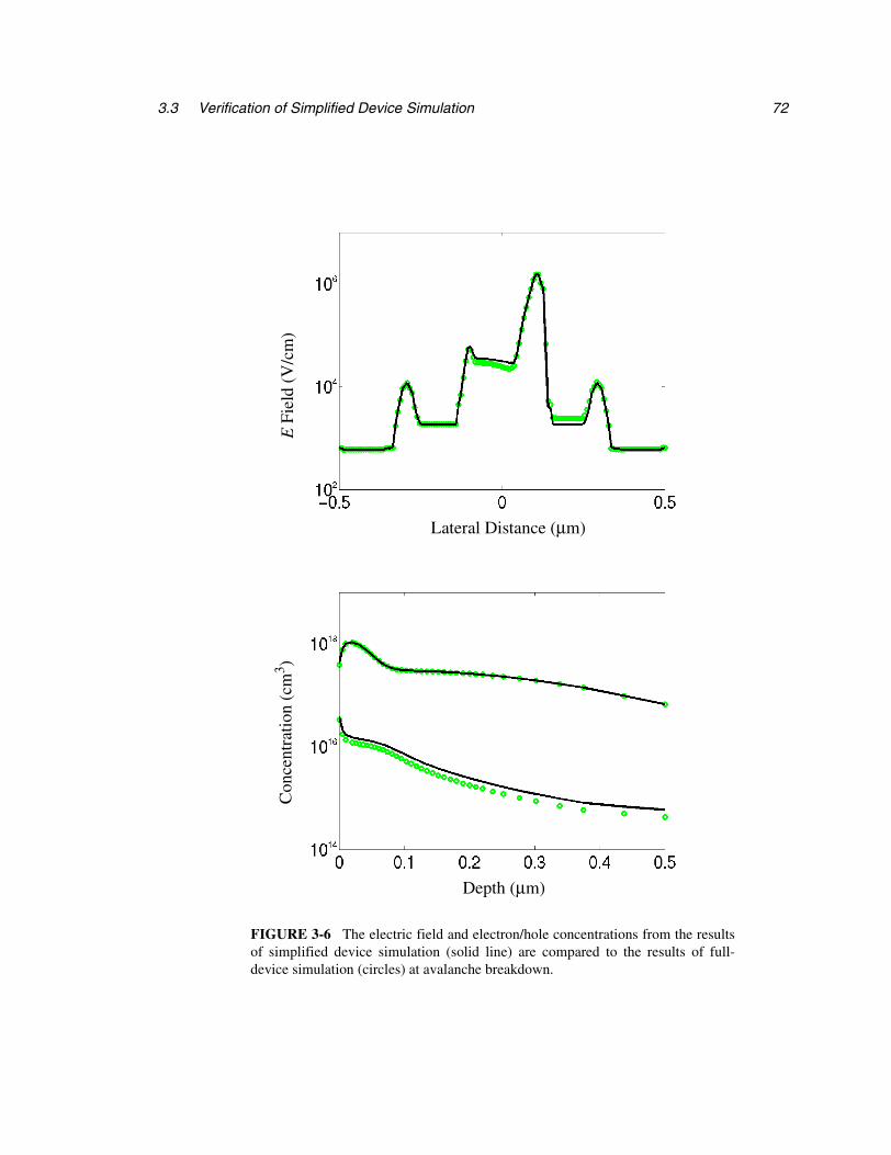
723.3 Verification of Simplified Device Simulation
Lateral Distance (µm)
E F
ield
(V
/cm
)
Depth (µm)
Con
cent
ratio
n (c
m3 )
FIGURE 3-6 The electric field and electron/hole concentrations from the resultsof simplified device simulation (solid line) are compared to the results of full-device simulation (circles) at avalanche breakdown.
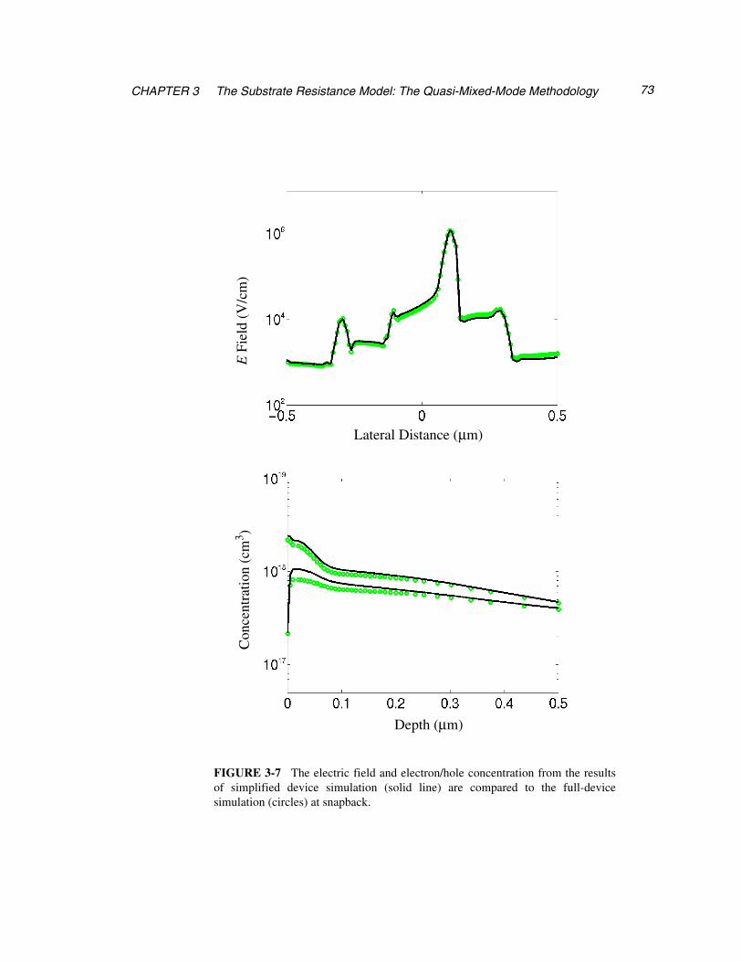
CHAPTER 3 The Substrate Resistance Model: The Quasi-Mixed-Mode Methodology 73
Lateral Distance (µm)
E F
ield
(V
/cm
)
Depth (µm)
Con
cent
ratio
n (c
m3 )
FIGURE 3-7 The electric field and electron/hole concentration from the resultsof simplified device simulation (solid line) are compared to the full-devicesimulation (circles) at snapback.
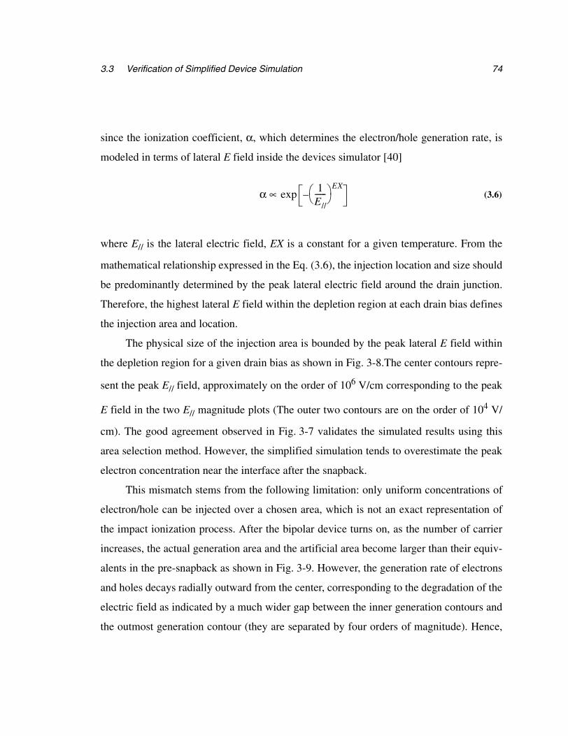
743.3 Verification of Simplified Device Simulation
since the ionization coefficient, α, which determines the electron/hole generation rate, is
modeled in terms of lateral E field inside the devices simulator [40]
where E// is the lateral electric field, EX is a constant for a given temperature. From the
mathematical relationship expressed in the Eq. (3.6), the injection location and size should
be predominantly determined by the peak lateral electric field around the drain junction.
Therefore, the highest lateral E field within the depletion region at each drain bias defines
the injection area and location.
The physical size of the injection area is bounded by the peak lateral E field within
the depletion region for a given drain bias as shown in Fig. 3-8.The center contours repre-
sent the peak E// field, approximately on the order of 106 V/cm corresponding to the peak
E field in the two E// magnitude plots (The outer two contours are on the order of 104 V/
cm). The good agreement observed in Fig. 3-7 validates the simulated results using this
area selection method. However, the simplified simulation tends to overestimate the peak
electron concentration near the interface after the snapback.
This mismatch stems from the following limitation: only uniform concentrations of
electron/hole can be injected over a chosen area, which is not an exact representation of
the impact ionization process. After the bipolar device turns on, as the number of carrier
increases, the actual generation area and the artificial area become larger than their equiv-
alents in the pre-snapback as shown in Fig. 3-9. However, the generation rate of electrons
and holes decays radially outward from the center, corresponding to the degradation of the
electric field as indicated by a much wider gap between the inner generation contours and
the outmost generation contour (they are separated by four orders of magnitude). Hence,
α 1E//------ EX
–exp∝ (3.6)

CHAPTER 3 The Substrate Resistance Model: The Quasi-Mixed-Mode Methodology 75
FIGURE 3-8 On the top plot, the E// contours show relative strength of the lateral Efield around the drain junction and the channel. The inner contours represent the peak E//
field as shown in the bottom two plots.
DrainSource
peak E field region
Vertical Distance (µm)
E// (
v/c
m)
Vertical Distancefor hole injection
Lateral Distance (µm)
E// (
v/c
m)
Lateral Distance for hole injection
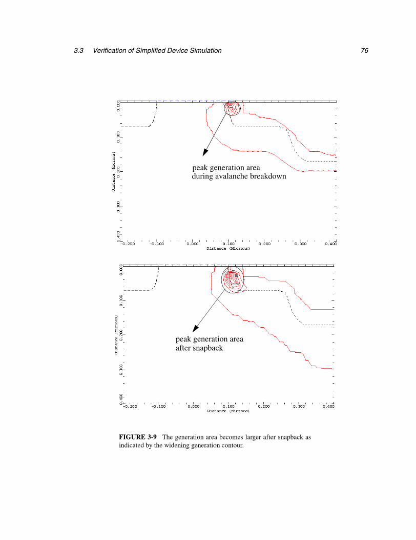
763.3 Verification of Simplified Device Simulation
FIGURE 3-9 The generation area becomes larger after snapback asindicated by the widening generation contour.
peak generation areaduring avalanche breakdown
peak generation areaafter snapback
CHAPTER 3 The Substrate Resistance Model: The Quasi-Mixed-Mode Methodology 77
the radially decaying generation rate would result in a slightly lower concentration near
the surface compared to the case of constant peak generation.
The overestimation can be corrected for by picking a larger injection area for the
same generation current, which would result in a lower concentration according to
Eq. (3.5). Thus, instead of picking the injection area according to the peak electric field,
the injection area bounded by the average E field is now considered. The average E field is
obtained as
where integrates the area under the E// curve along either the x or y direction as
shown in Fig. 3-8, d is the respective values on either the x- or y-axis. Using the injection
area bounded by the average E field, it is observed that the resulting electron concentration
agrees with the results from full-impact ionization simulation to within 5% as shown in
Fig. 3-10. Because of the intensity of the E field, even though the injection area varied by
30% switching from area bounded by peak E field to average E field, the resulting peak
electron concentration differs only by 4%.
Having verified the artificial injection method, the overall QMM methodology is
evaluated by attempting to simulate the ESD I-V characteristics of the protection device.
3.4 QMM METHOD VS. FULL DEVICE SIMULATION
The Quasi-Mixed-Mode model is now applied in the modeling of the 0.25µm device
used in the last section to verify the ESD I-V curves using both the QMM method and full-
device simulation. In order to test the layout dependent simulation capability of the QMM
Eavg
E//
d∫
d---------= (3.7)
E//∫
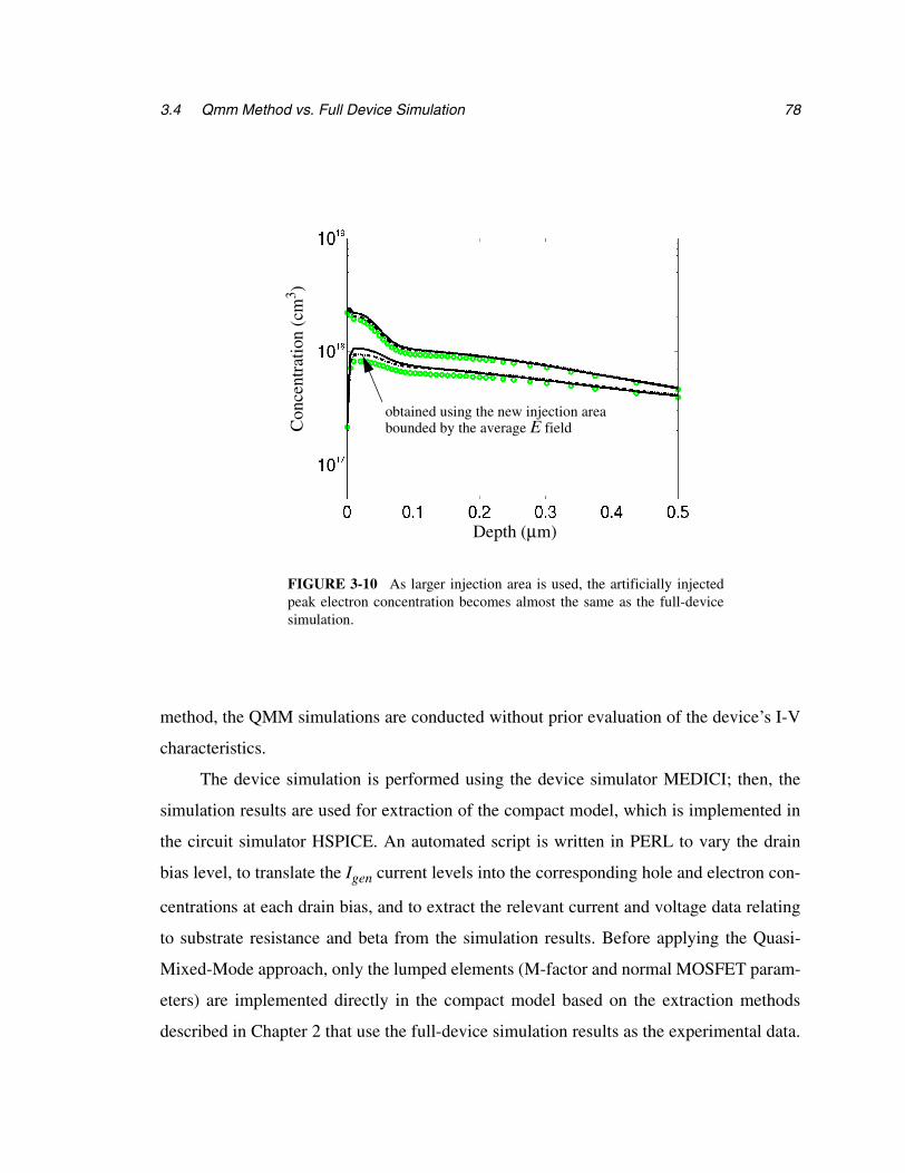
783.4 Qmm Method vs. Full Device Simulation
method, the QMM simulations are conducted without prior evaluation of the device’s I-V
characteristics.
The device simulation is performed using the device simulator MEDICI; then, the
simulation results are used for extraction of the compact model, which is implemented in
the circuit simulator HSPICE. An automated script is written in PERL to vary the drain
bias level, to translate the Igen current levels into the corresponding hole and electron con-
centrations at each drain bias, and to extract the relevant current and voltage data relating
to substrate resistance and beta from the simulation results. Before applying the Quasi-
Mixed-Mode approach, only the lumped elements (M-factor and normal MOSFET param-
eters) are implemented directly in the compact model based on the extraction methods
described in Chapter 2 that use the full-device simulation results as the experimental data.
FIGURE 3-10 As larger injection area is used, the artificially injectedpeak electron concentration becomes almost the same as the full-devicesimulation.
obtained using the new injection areabounded by the average E field
Depth (µm)
Con
cent
ratio
n (c
m3 )

CHAPTER 3 The Substrate Resistance Model: The Quasi-Mixed-Mode Methodology 79
The geometric (layout) dependent parameters, such as the substrate resistance and beta,
are obtained from the QMM simulation results that are not based on the data from the full
simulation.
The 2-D cross-section of the device with the grid is shown in Fig. 3-11. After placing
the boundary condition and artificially injecting the generated carriers at different drain
biases and performing the simplified device simulations, a family of Isub vs. Id curves at
FIGURE 3-11 A two-dimensional cross section of the virtual device used inthe verification of the QMM method with grid. Denser grid is placed around thechannel and junction region to accurately simulate the hole injection process.
Gate DrainSourceSubstrate Tap
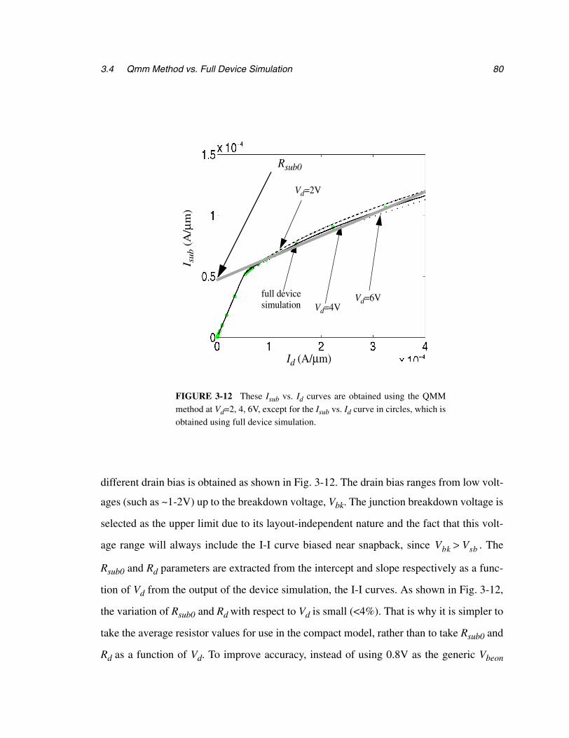
803.4 Qmm Method vs. Full Device Simulation
different drain bias is obtained as shown in Fig. 3-12. The drain bias ranges from low volt-
ages (such as ~1-2V) up to the breakdown voltage, Vbk. The junction breakdown voltage is
selected as the upper limit due to its layout-independent nature and the fact that this volt-
age range will always include the I-I curve biased near snapback, since . The
Rsub0 and Rd parameters are extracted from the intercept and slope respectively as a func-
tion of Vd from the output of the device simulation, the I-I curves. As shown in Fig. 3-12,
the variation of Rsub0 and Rd with respect to Vd is small (<4%). That is why it is simpler to
take the average resistor values for use in the compact model, rather than to take Rsub0 and
Rd as a function of Vd. To improve accuracy, instead of using 0.8V as the generic Vbeon
FIGURE 3-12 These Isub vs. Id curves are obtained using the QMM
method at Vd=2, 4, 6V, except for the Isub vs. Id curve in circles, which isobtained using full device simulation.
I sub
(A
/µm
)
Id (A/µm)
Vd=2V
Vd=4VVd=6Vfull device
simulation
Rsub0
Vbk Vsb>
CHAPTER 3 The Substrate Resistance Model: The Quasi-Mixed-Mode Methodology 81
voltage used in the extraction of Rsub0, as demonstrated in Eq. (2.19) in Chapter 2, the cor-
responding Vsub can be obtained from the device simulation results for each substrate cur-
rent. In this case, Rsub0 is found to be 20.5kΩ-µm; Rd is found to be 3.5kΩ-µm. The
extracted Rsub0 and Rd parameters are then implemented into the substrate current-con-
trolled-voltage-sources inside the compact models as illustrated in Eq. (3.2).
The β of the parasitic bipolar device can also be obtained from the Isub vs. Id curve.
Since the generation current is known as an input, the base current, Ib can be calculated as
follows
the collector current, Ic can be calculated as
Dividing Eq. (3.9) by Eq. (3.8), β can be calculated for each drain voltage as
The resulting β plotted as a function of Ic at different drain bias is shown in Fig. 3-13. As
expected, the magnitude of β increases initially with the drain voltage due to the reduction
of the base width as a result of the widening of the depletion region between the drain
(collector) and substrate (base). The three β curves start to rapidly decrease and begin to
merge together as the bipolar moves into the high-current injection phase due to the rapid
increase of the collector current. The roll-off of the β as Ic increases and the variation of β
Ib Vd( ) Igen Vd( ) Isub Vd( )–= (3.8)
Ic Vd( ) Id Vd( ) Igen Vd( )–= (3.9)
β Vd( )Ic Vd( )Ib Vd( )---------------= (3.10)

823.4 Qmm Method vs. Full Device Simulation
with respect to Vd (=Vce) can also be modeled in the bipolar circuit model.
After implementing the substrate resistance and β models, the high current charac-
teristics of the device can be simulated. As can be seen from the plot shown in Fig. 3-14,
the high-current I-V curves obtained using the QMM method match closely to the I-V
curves obtained using the full-device simulation, demonstrating the accuracy of the QMM
methodology.
The above device has only one substrate contact on the source side where Rsub0 and
Rd did not exhibit much change with respect to the varying drain biases, simplifying the
application of the methodology. Rsub0 and Rd need to be implemented as a function of the
drain bias for multiple substrate contacts. Usually more substrate taps are added to the on-
chip ESD protection device in order to suppress concurrent ESD induced latch-up issues
FIGURE 3-13 These are β vs. Ic curves obtained using QMMsimulation at Vd=2, 4, 6V.
β
Ic (A/µm)
Vd=6V
Vd=2VVd=4V
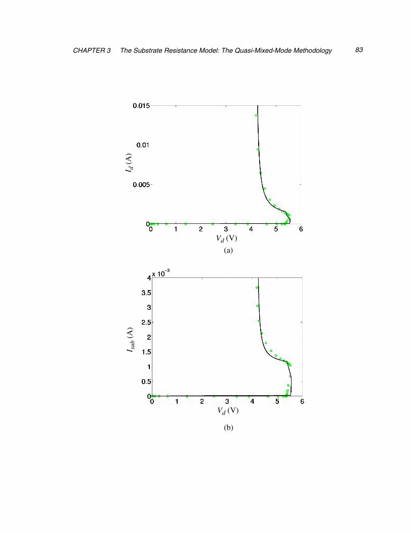
CHAPTER 3 The Substrate Resistance Model: The Quasi-Mixed-Mode Methodology 83
Vd (V)
I sub
(A
)
Vd (V)
I d (
A)
(b)
(a)
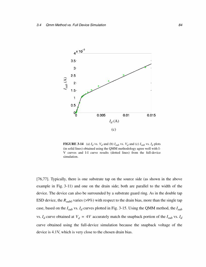
843.4 Qmm Method vs. Full Device Simulation
[76,77]. Typically, there is one substrate tap on the source side (as shown in the above
example in Fig. 3-11) and one on the drain side; both are parallel to the width of the
device. The device can also be surrounded by a substrate guard ring. As in the double tap
ESD device, the Rsub0 varies (>9%) with respect to the drain bias, more than the single tap
case, based on the Isub vs. Id curves plotted in Fig. 3-15. Using the QMM method, the Isub
vs. Id curve obtained at accurately match the snapback portion of the Isub vs. Id
curve obtained using the full-device simulation because the snapback voltage of the
device is 4.1V, which is very close to the chosen drain bias.
Id (A)
I sub
(A
)
FIGURE 3-14 (a) Id vs. Vd and (b) Isub vs. Vd and (c) Isub vs. Id plots(in solid lines) obtained using the QMM methodology agree well with I-V curves and I-I curve results (dotted lines) from the full-devicesimulation.
(c)
Vd 4V=

CHAPTER 3 The Substrate Resistance Model: The Quasi-Mixed-Mode Methodology 85
Comparing Fig. 3-12 and Fig. 3-15, we show that the Rsub0s from the double tapped
structure varies significantly with the applied drain bias. This variation of Rsub0 with
respect to the drain bias is plotted in Fig. 3-16. The additional tap next to the drain contrib-
uted to this Rsub0 variation. Without the drain bias, the Rsub0 would be roughly halved as
the drain and source taps contributed equally. However, as the drain bias increases, the
Rsub0 value increases from the its intrinsic resistance value at because the increas-
ing E field at the drain junction sweeps more holes toward the source side. Therefore, rel-
atively less substrate current flows to the drain side tap as compared to the case at the
lower drain bias, resulting in an increased Rsub0. Also shown in Fig. 3-15, the slope of the
FIGURE 3-15 Comparison of Isub vs. Id (lines) curvesobtained using the QMM methodology against Isub vs. Id
(circles) obtained using full device simulation for the devicewith two substrate taps.
I sub
(A
/µm
)
Id (A/µm)
Vd=2V
Vd=6VVd=4V
Vd 0=
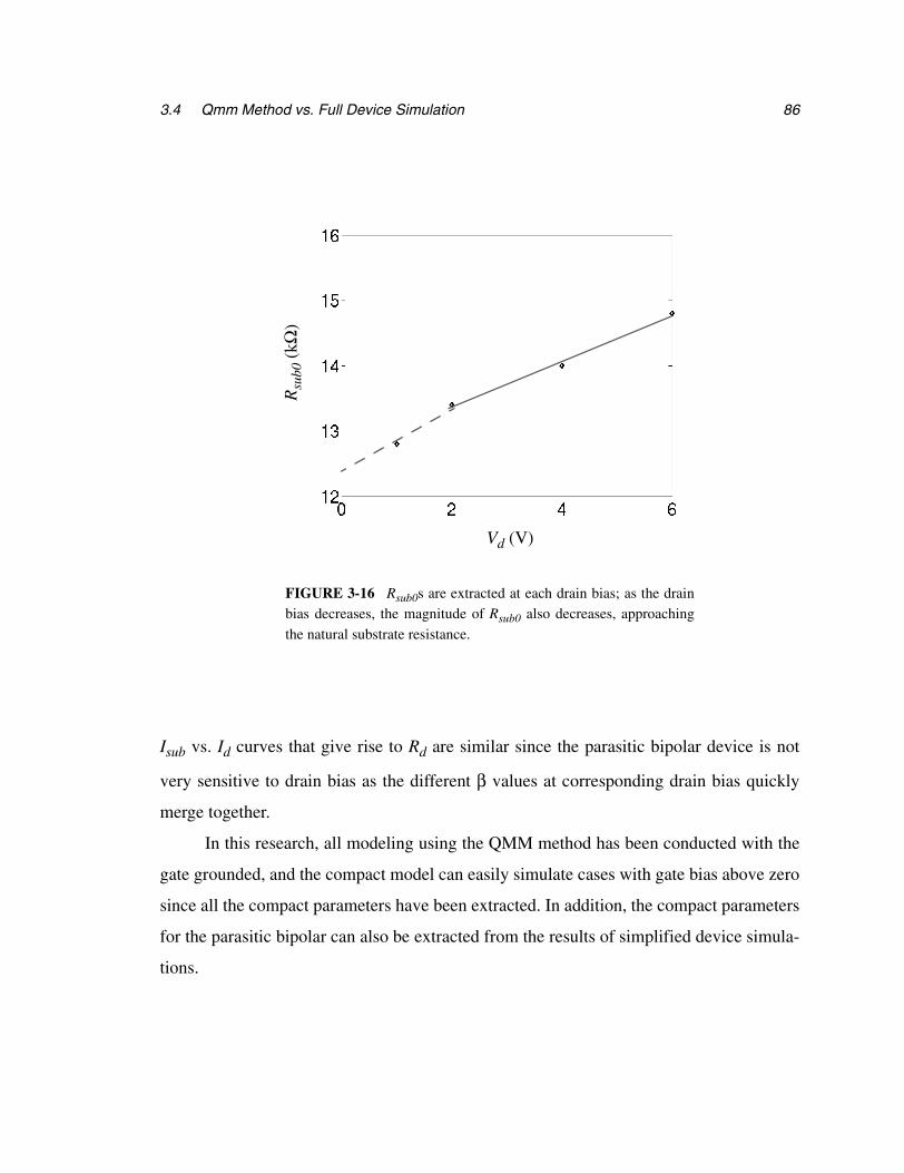
863.4 Qmm Method vs. Full Device Simulation
Isub vs. Id curves that give rise to Rd are similar since the parasitic bipolar device is not
very sensitive to drain bias as the different β values at corresponding drain bias quickly
merge together.
In this research, all modeling using the QMM method has been conducted with the
gate grounded, and the compact model can easily simulate cases with gate bias above zero
since all the compact parameters have been extracted. In addition, the compact parameters
for the parasitic bipolar can also be extracted from the results of simplified device simula-
tions.
FIGURE 3-16 Rsub0s are extracted at each drain bias; as the drainbias decreases, the magnitude of Rsub0 also decreases, approaching
the natural substrate resistance.
Vd (V)
Rsu
b0 (
kΩ)
CHAPTER 3 The Substrate Resistance Model: The Quasi-Mixed-Mode Methodology 87
3.5 DISCUSSION OF THE QMM APPROACH
The Quasi-Mixed-Mode methodology aims to bring layout dependent modeling
capability into ESD compact model by utilizing the lumped nature of the impact ioniza-
tion multiplication factor M in terms of the process technology as well as employing the
layout dependent nature of the substrate resistance and the current gain β of the parasitic
bipolar. The QMM method exploits both circuit and device simulators, offering a good
trade off between using a physics based model and being computationally robust and effi-
cient as shown below:
• Geometric Scalability−Similar to the full device simulator, the QMM approach models
geometry scaling by simulating corresponding substrate resistance and β from a realis-
tic 2-D cross-section of the protection device. On the other hand, the compact model
alone does not simulate layout variations since its parameters are extracted from exper-
imental data as fixed values.
• Ease of Calibration−Calibration of the doping profile for device simulation is equiva-
lent to extraction of model parameters for circuit simulation albeit not as simple. The
doping profile for a given device (and process technology) is calibrated by tuning the
doping profile such that the simulation results of the device simulation match the exper-
imental data. During the junction breakdown process, the highly non-linear relationship
between the drain bias and the generated carriers makes the accurate calibration of the
doping profile difficult. By simplifying the device simulation to inject a hole current
instead of simulating the complete junction breakdown process, it becomes easier to
calibrate the doping profile since we are not required to simulate the impact ionization
action, thus overcoming the more stringent calibration requirements.
• Device Physics−Compared to full fledged device simulation, the QMM method only
simulates the operation of the parasitic bipolar device, trading off simulation of impact
ionization in device simulation for the ease of calibration. The QMM method is a good
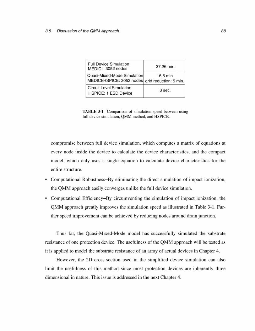
883.5 Discussion of the QMM Approach
compromise between full device simulation, which computes a matrix of equations at
every node inside the device to calculate the device characteristics, and the compact
model, which only uses a single equation to calculate device characteristics for the
entire structure.
• Computational Robustness−By eliminating the direct simulation of impact ionization,
the QMM approach easily converges unlike the full device simulation.
• Computational Efficiency−By circumventing the simulation of impact ionization, the
QMM approach greatly improves the simulation speed as illustrated in Table 3-1. Fur-
ther speed improvement can be achieved by reducing nodes around drain junction.
Thus far, the Quasi-Mixed-Mode model has successfully simulated the substrate
resistance of one protection device. The usefulness of the QMM approach will be tested as
it is applied to model the substrate resistance of an array of actual devices in Chapter 4.
However, the 2D cross-section used in the simplified device simulation can also
limit the usefulness of this method since most protection devices are inherently three
dimensional in nature. This issue is addressed in the next Chapter 4.
Full Device Simulation3052 nodesMEDICI:
Quasi-Mixed-Mode SimulationMEDICI/HSPICE: 3052 nodes
Circuit Level SimulationHSPICE: 1 ESD Device
37.26 min.
16.5 mingrid reduction: 5 min.
3 sec.
TABLE 3-1 Comparison of simulation speed between usingfull device simulation, QMM method, and HSPICE.

CHAPTER 3 The Substrate Resistance Model: The Quasi-Mixed-Mode Methodology 89

CHAPTER 4
CALIBRATION AND SIMULATION OF SUBSTRATE RESISTANCE USING THE QMM
METHODOLOGY
4.1 CALIBRATION AND SIMULATION OF SUBSTRATE RESISTANCE
FOR SINGLE-FINGER DEVICES
In the previous chapter, the QMM methodology was presented, and its accuracy was
verified against full-device simulations. In this chapter, the QMM method is applied to
simulate the substrate resistances of various real devices.
Modeling the substrate resistance for the single-finger devices is first considered
with respect to geometric and process variations. Two sets of single-finger devices with
identical layout are fabricated using state-of-the-art CMOS technology with two different
p-well dopings; process X has a p-well doping lower than that for process Y. These ESD
devices are all 20µm wide with varying gate lengths (Lch) or source to substrate contact
89
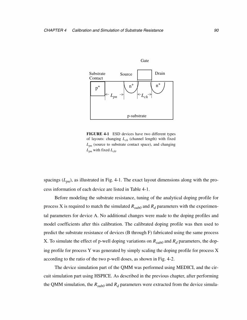
CHAPTER 4 Calibration and Simulation of Substrate Resistance 90
spacings (Lpn), as illustrated in Fig. 4-1. The exact layout dimensions along with the pro-
cess information of each device are listed in Table 4-1.
Before modeling the substrate resistance, tuning of the analytical doping profile for
process X is required to match the simulated Rsub0 and Rd parameters with the experimen-
tal parameters for device A. No additional changes were made to the doping profiles and
model coefficients after this calibration. The calibrated doping profile was then used to
predict the substrate resistance of devices (B through F) fabricated using the same process
X. To simulate the effect of p-well doping variations on Rsub0 and Rd parameters, the dop-
ing profile for process Y was generated by simply scaling the doping profile for process X
according to the ratio of the two p-well doses, as shown in Fig. 4-2.
The device simulation part of the QMM was performed using MEDICI, and the cir-
cuit simulation part using HSPICE. As described in the previous chapter, after performing
the QMM simulation, the Rsub0 and Rd parameters were extracted from the device simula-
Gate
Substrate
p-substrate
n+p+ n+
Source Drain
LchLpn
Contact
FIGURE 4-1 ESD devices have two different typesof layouts: changing Lch (channel length) with fixed
Lpn (source to substrate contact space), and changingLpn with fixed Lch.
914.1 Calibration and Simulation of Substrate Resistance for Single-Finger Devices
tion results. The experimental Rsub0 and Rd parameters for devices A and B were extracted
based on Eqs. (2.19) and (2.20) as shown in Fig. 4-3; the Rsub0 and Rd parameters of
devices G and H were extracted using the same method. The predicted Rsub0 values
obtained using the QMM method are plotted against the extracted Rsub0 as shown in
Fig. 4-4.
The experimental Rsub0 and Rd parameters for devices C and D were extracted as
shown in Fig. 4-5, and similarly the Rsub0 and Rd parameters of devices E and F and I
through L were extracted using the same method. The predicted Rsub0 and Rd values
Process X Process Y
Devices DevicesLch Lpn Lch Lpn
A
B
C
D
E
G
H
I
J
K
0.21 2.5 0.21 2.5
0.21 10 0.21 10
0.18 2.3 0.18 2.3
0.21 0.212.3 2.3
0.25 2.3 0.25 2.3
F 0.30 2.3 0.30 2.3 L
TABLE 4-1 Devices A-L have the same layoutdimensions, aside from the different dimensions listed. Allthe dimensions listed in the Table 1 are in µm. Process Xdiffers from process Y only in p-well dose. Devices A-Fare fabricated using process X, and devices G-L arefabricated using process Y.
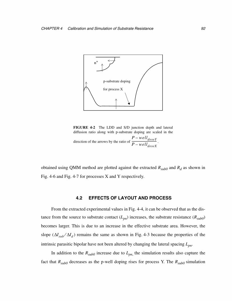
CHAPTER 4 Calibration and Simulation of Substrate Resistance 92
obtained using QMM method are plotted against the extracted Rsub0 and Rd as shown in
Fig. 4-6 and Fig. 4-7 for processes X and Y respectively.
4.2 EFFECTS OF LAYOUT AND PROCESS
From the extracted experimental values in Fig. 4-4, it can be observed that as the dis-
tance from the source to substrate contact (Lpn) increases, the substrate resistance (Rsub0)
becomes larger. This is due to an increase in the effective substrate area. However, the
slope ( ) remains the same as shown in Fig. 4-3 because the properties of the
intrinsic parasitic bipolar have not been altered by changing the lateral spacing Lpn.
In addition to the Rsub0 increase due to Lpn, the simulation results also capture the
fact that Rsub0 decreases as the p-well doping rises for process Y. The Rsub0 simulation
n+
p-substrate doping
for process X
FIGURE 4-2 The LDD and S/D junction depth and lateraldiffusion ratio along with p-substrate doping are scaled in the
direction of the arrows by the ratio of .P well– doseY
P well– doseX---------------------------------
Isub∆ Id∆⁄
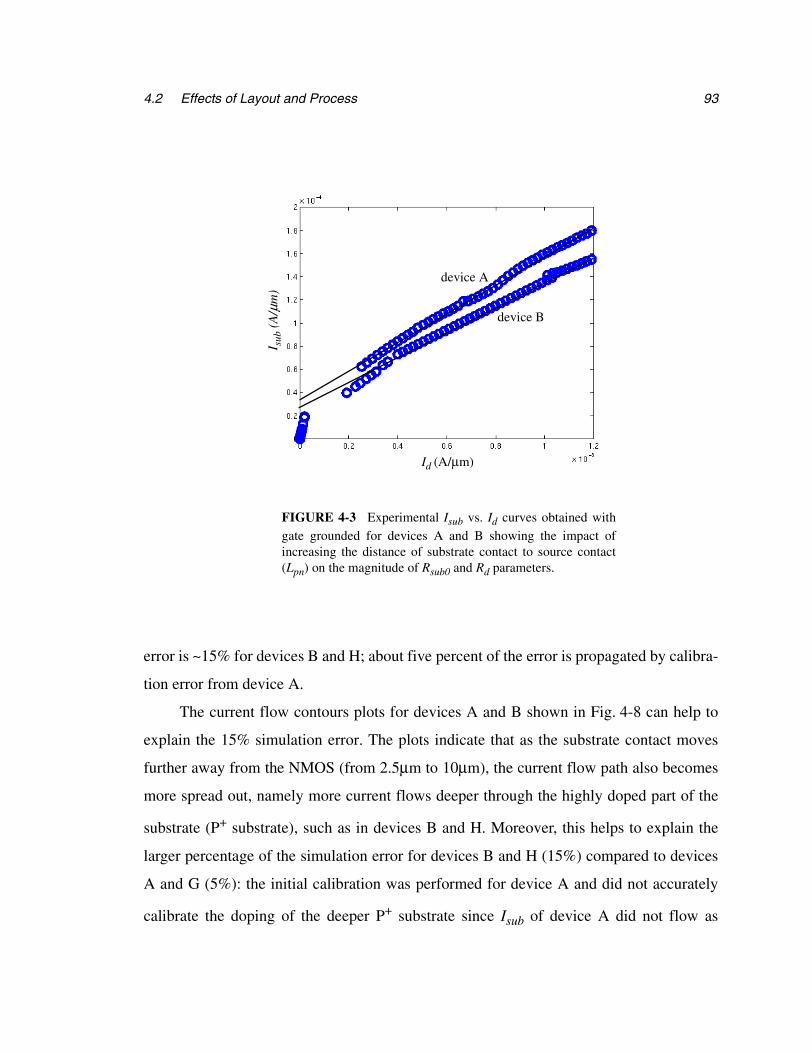
934.2 Effects of Layout and Process
error is ~15% for devices B and H; about five percent of the error is propagated by calibra-
tion error from device A.
The current flow contours plots for devices A and B shown in Fig. 4-8 can help to
explain the 15% simulation error. The plots indicate that as the substrate contact moves
further away from the NMOS (from 2.5µm to 10µm), the current flow path also becomes
more spread out, namely more current flows deeper through the highly doped part of the
substrate (P+ substrate), such as in devices B and H. Moreover, this helps to explain the
larger percentage of the simulation error for devices B and H (15%) compared to devices
A and G (5%): the initial calibration was performed for device A and did not accurately
calibrate the doping of the deeper P+ substrate since Isub of device A did not flow as
Id (A/µm)
device A
device B
I sub
(A
/µm
)
FIGURE 4-3 Experimental Isub vs. Id curves obtained withgate grounded for devices A and B showing the impact ofincreasing the distance of substrate contact to source contact(Lpn) on the magnitude of Rsub0 and Rd parameters.
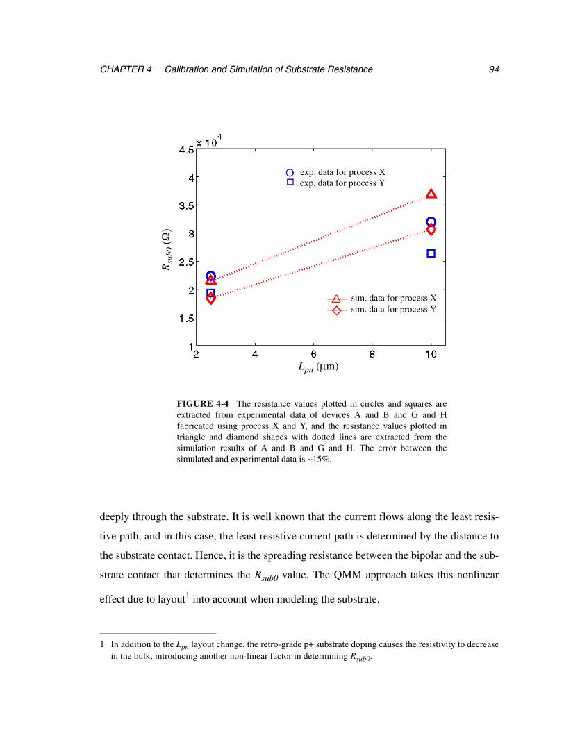
CHAPTER 4 Calibration and Simulation of Substrate Resistance 94
deeply through the substrate. It is well known that the current flows along the least resis-
tive path, and in this case, the least resistive current path is determined by the distance to
the substrate contact. Hence, it is the spreading resistance between the bipolar and the sub-
strate contact that determines the Rsub0 value. The QMM approach takes this nonlinear
effect due to layout1 into account when modeling the substrate.
1 In addition to the Lpn layout change, the retro-grade p+ substrate doping causes the resistivity to decreasein the bulk, introducing another non-linear factor in determining Rsub0.
Rsu
b0 (Ω
)
Lpn (µm)
exp. data for process Xexp. data for process Y
sim. data for process Xsim. data for process Y
FIGURE 4-4 The resistance values plotted in circles and squares areextracted from experimental data of devices A and B and G and Hfabricated using process X and Y, and the resistance values plotted intriangle and diamond shapes with dotted lines are extracted from thesimulation results of A and B and G and H. The error between thesimulated and experimental data is ~15%.
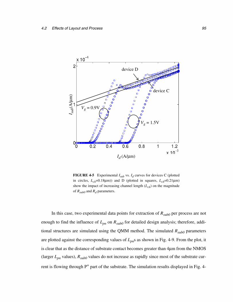
954.2 Effects of Layout and Process
In this case, two experimental data points for extraction of Rsub0 per process are not
enough to find the influence of Lpn on Rsub0 for detailed design analysis; therefore, addi-
tional structures are simulated using the QMM method. The simulated Rsub0 parameters
are plotted against the corresponding values of Lpns as shown in Fig. 4-9. From the plot, it
is clear that as the distance of substrate contact becomes greater than 4µm from the NMOS
(larger Lpn values), Rsub0 values do not increase as rapidly since most of the substrate cur-
rent is flowing through P+ part of the substrate. The simulation results displayed in Fig. 4-
Id (A/µm)
I sub
(A/µ
m)
Vg = 0.9V
Vg = 1.5V
device D
device C
FIGURE 4-5 Experimental Isub vs. Id curves for devices C (plottedin circles, Lch=0.18µm)) and D (plotted in squares, Lch=0.21µm)
show the impact of increasing channel length (Lch) on the magnitudeof Rsub0 and Rd parameters.
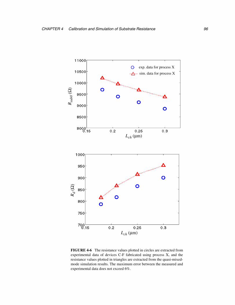
CHAPTER 4 Calibration and Simulation of Substrate Resistance 96
Lch (µm)
Rd (
Ω)
Rsu
b0 (Ω
)exp. data for process X
sim. data for process X
FIGURE 4-6 The resistance values plotted in circles are extracted fromexperimental data of devices C-F fabricated using process X, and theresistance values plotted in triangles are extracted from the quasi-mixed-mode simulation results. The maximum error between the measured andexperimental data does not exceed 6%.
Lch (µm)
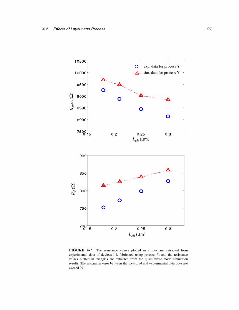
974.2 Effects of Layout and Process
Lch (µm)
exp. data for process Y
sim. data for process Y R
d (Ω
) R
sub0
(Ω)
FIGURE 4-7 The resistance values plotted in circles are extracted fromexperimental data of devices I-L fabricated using process Y, and the resistancevalues plotted in triangles are extracted from the quasi-mixed-mode simulationresults. The maximum error between the measured and experimental data does notexceed 9%.
Lch (µm)
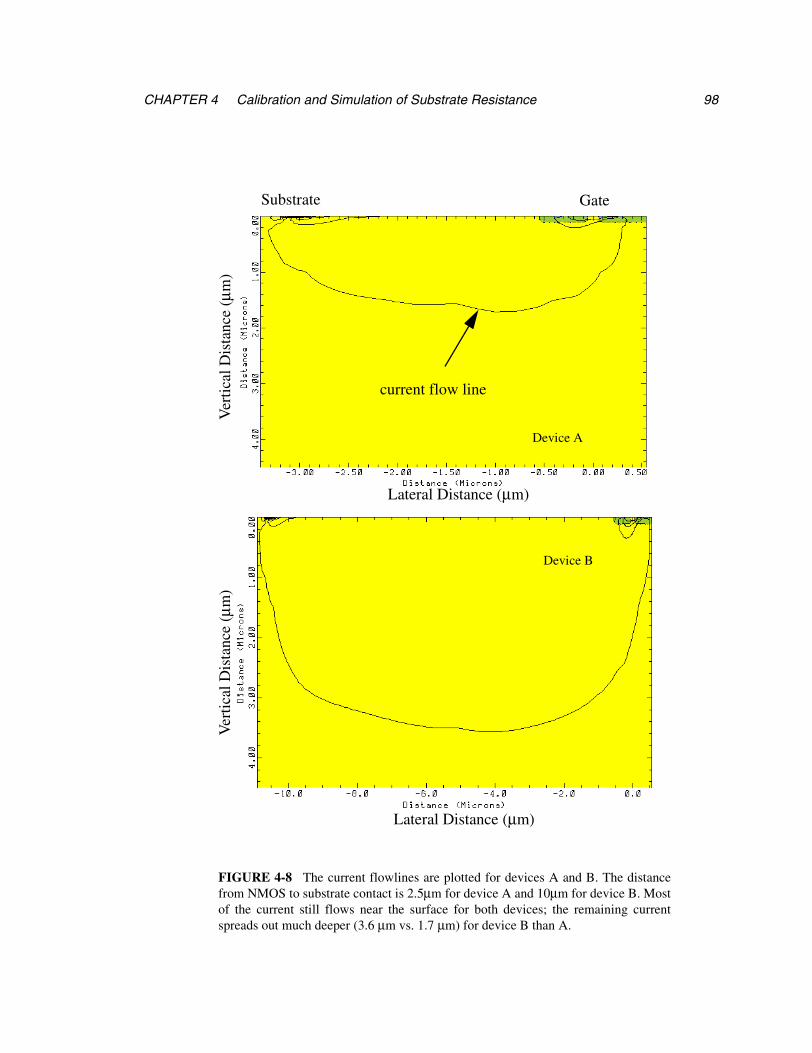
CHAPTER 4 Calibration and Simulation of Substrate Resistance 98
GateSubstrate
current flow line
Device A
Device B
Ver
tica
l Dis
tanc
e (µ
m)
Lateral Distance (µm)
FIGURE 4-8 The current flowlines are plotted for devices A and B. The distancefrom NMOS to substrate contact is 2.5µm for device A and 10µm for device B. Mostof the current still flows near the surface for both devices; the remaining currentspreads out much deeper (3.6 µm vs. 1.7 µm) for device B than A.
Ver
tica
l Dis
tanc
e (µ
m)
Lateral Distance (µm)
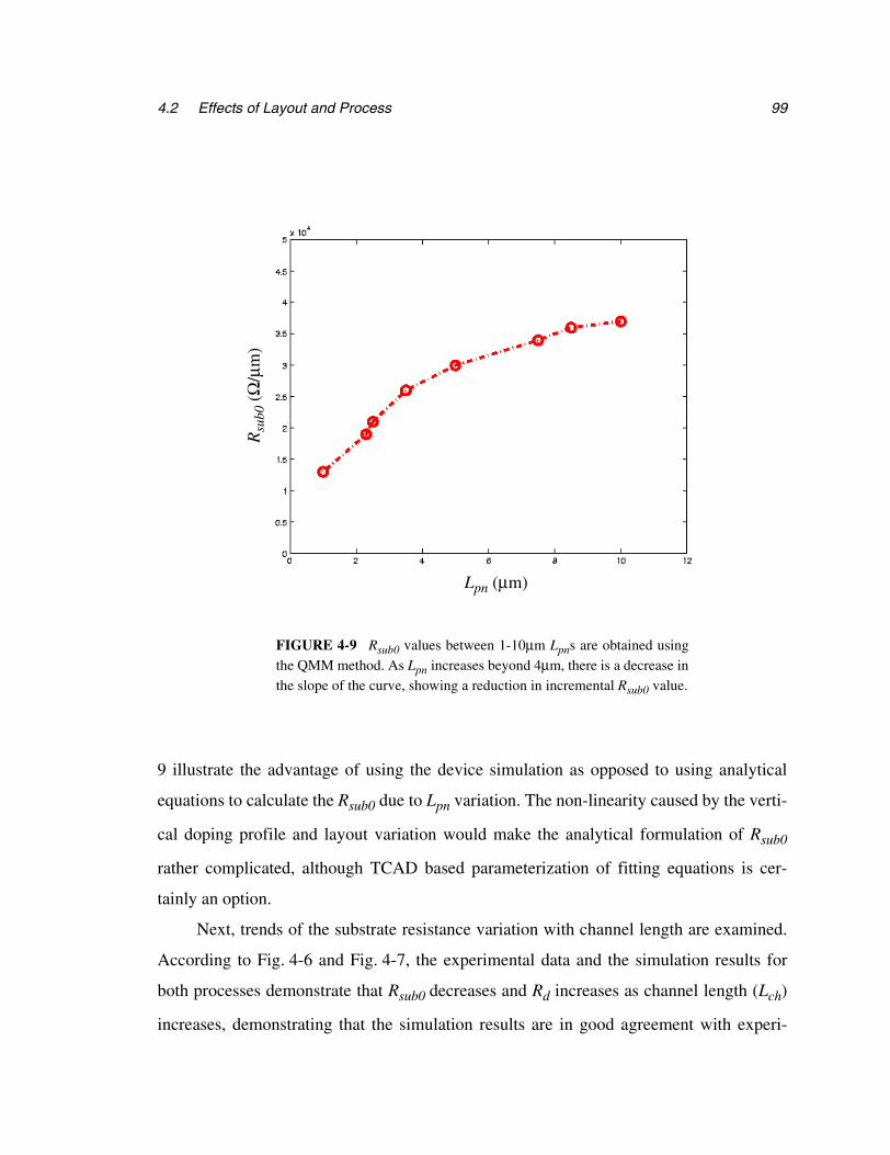
994.2 Effects of Layout and Process
9 illustrate the advantage of using the device simulation as opposed to using analytical
equations to calculate the Rsub0 due to Lpn variation. The non-linearity caused by the verti-
cal doping profile and layout variation would make the analytical formulation of Rsub0
rather complicated, although TCAD based parameterization of fitting equations is cer-
tainly an option.
Next, trends of the substrate resistance variation with channel length are examined.
According to Fig. 4-6 and Fig. 4-7, the experimental data and the simulation results for
both processes demonstrate that Rsub0 decreases and Rd increases as channel length (Lch)
increases, demonstrating that the simulation results are in good agreement with experi-
FIGURE 4-9 Rsub0 values between 1-10µm Lpns are obtained usingthe QMM method. As Lpn increases beyond 4µm, there is a decrease inthe slope of the curve, showing a reduction in incremental Rsub0 value.
Lpn (µm)
Rsu
b0 (
Ω/µ
m)

CHAPTER 4 Calibration and Simulation of Substrate Resistance 100
mental data. As the p-well doping increases for process Y, the magnitude of simulated
Rsub0 values in Fig. 4-7 also decrease compared to that of Fig. 4-6 (process X). The per-
centage errors for devices C through F and I through L, which all have different Lch, are
less than 9%. The error might be caused by the inaccuracies in the 2-D doping profile.
As illustrated in Fig. 4-3, Rsub0 is the substrate resistance at the turn-on for the para-
sitic bipolar (i.e. ). At this point, the generation current, Igen can be
expressed as
and the injected hole current (Igen) flows from the drain junction towards the substrate
contact. The substrate spreading resistance (Rsub0) can be estimated using the following
expression [35],
where ρ is the substrate resistivity, T is the substrate depth, Xj is the junction depth, Xd is
the depletion width at the drain junction, w is the channel width, and Lch is the channel
length. The exact relation between L’ and Lch in Eq. (4.3) depends on the hole current dis-
tribution inside the substrate, which can be obtained by empirically fitting calculated
Rsub0s in Eq. (4.2) to the experimental values [35]. Together Eqs. (4.2) and (4.3) demon-
Ic Ib 0= =
Igen Isub= (4.1)
Rsub0 ρ⁄ 12 W Lch–( )---------------------------
W Lch 2T+( )Lch W 2T+( )------------------------------- ln
Xj Xd 2⁄+
W L′( )
------------------------+= (4.2)
L Lch∝ (4.3)

1014.2 Effects of Layout and Process
strate that the magnitude of Rsub0 decreases with channel length.
On the other hand, the slope Rd increases because the current gain β of the parasitic
BJT decreases more rapidly as the drain current increases for shorter channel lengths as
shown in Fig. 4-10. It also can be shown that during snapback [29,35,81],
FIGURE 4-10 β for devices C and F are extracted from the QMMsimulation results. β of device C decreases at a much faster rate thandevice F; hence, the percent increase in Ib is larger as the Id increases fordevice C.
Id (A/µm)
βLch=0.18µm (Device C)
Lch=0.30µm (Device F)
β
β M 1–( )⋅ 1≥ (4.4)
CHAPTER 4 Calibration and Simulation of Substrate Resistance 102
As β decreases due to high-current injection for both the short and long channel
devices−for example devices C and F−M increases for both as governed by Eq. (4.4) to
keep the parasitic BJT on. Therefore, Igen increases, but because at
each Id according to Eq. (4.5). Ib also increases as β decreases, but the rate of increase for
IbF is less than that of IbC because the rate of decrease of βF is much less than that of βC.
Hence, the slope of the Isub vs. Id curve decreases as the sharp drop in β requires more Ib
(Eq. (4.6)) from Igen for shorter channel length devices [80].
The current gain degradation in C and F is caused by high-current injection after the
parasitic BJT turns on. During this process, the injection of electrons into the base is suffi-
cient to cause a significant increase in the hole concentration in the base, thereby reducing
the collector current (Ic). The base charge under high-current injection can be described by
[48],
Igen M 1–( ) Ic Ids+( )⋅= (4.5)
βIc
Ib----= (4.6)
IgenC IgenF< βC βF>
p x( ) xd
0
xB
∫ Na x( ) n′
x( )+ xd
0
xB
∫= (4.7)
xB Lch∝ (4.8)
1034.3 Motivation for 3D Substrate Resistance Model
where is the Gummel Number, the initial built-in base charge caused by the
processing of the transistor, xB is the width of the quasi-neutral region of the base, and
is the injected electron concentration. Based on Eqs. (4.7) and (4.8), Device F with
the longer Lch has a larger Gummel Number than Device C, resulting in a lower β as
shown in Fig. 4-10, but for the incremental β change (β degradation) during high-current
injection, the device with a larger Gummel Number (large-base charge) is less affected by
the injected electrons than the device with a smaller Gummel Number (small-base
charge); hence, the β degrades at a slower rate for longer-channel devices.
Rsub0 and Rd vary according to the changes in the process and layout as can be seen
from Fig. 4-4, Fig. 4-6, and Fig. 4-7. The changes in Rsub0 and Rd are reflected in the
shape of ESD I-V curves. The QMM method can accurately model the changes in the I-V
curves based on the simulated Rsub0 and Rd values. For example, before introducing the
QMM method, in order to quantitatively predict the changes in the I-V curve when we
increase Lch from 0.18µm (Device C) to 0.30µm (Device F) without fabricating Device F,
Rsub0 and Rd from Device C was used due to the lack of Rsub0 and Rd information on
Device F. Using the QMM method, Rsub0 and Rd for Device F can be predicted resulting in
a more accurate ESD I-V curve as shown in Fig. 4-11.
4.3 MOTIVATION FOR 3D SUBSTRATE RESISTANCE MODEL
It has been demonstrated that the Quasi-Mixed-Mode methodology is a useful tool
that can be used to simulate the substrate resistance as well as the high-current characteris-
tics of deep submicron devices with process and geometry variations. However, the 2D
device simulator inside the QMM method limits the range of the devices that can be simu-
lated to those with uniform 2D cross-sections. A 3D structure can be reduced to a 2D
Na x( ) xd0
xB∫
n′
x( )
CHAPTER 4 Calibration and Simulation of Substrate Resistance 104
cross-section for the simulation of the ESD high current characteristics by slicing perpen-
dicular into the device width direction1.
Typically in CMOS technology, the slices of the 2D cross-sections are identical for
the intrinsic 3D device formed by the drain, channel, and source; however, the placement
of the substrate contact, or the substrate tap, around the intrinsic device can cause the cur-
rent conduction uniformity assumption to be invalid, thus introducing 3D geometry effects
that cannot be simulated with 2D device simulator. Typically, the substrate taps are placed
either parallel or perpendicular to the width of the intrinsic device, or enclose the intrinsic
device totally, acting as a guard ring. So far, the devices that have been modeled using the
QMM approach all have the parallel substrate tap placement, which enables the substrate
current to flow uniformly along the width, allowing the reduction of the 3D device to the
2D cross-sections. Each slice has the same substrate resistance. On the other hand, the per-
pendicular and totally enclosed contact geometries cause the substrate resistance to vary
along the width, making the reduction to 2D impossible.
As shown in the Fig. 4-12, the comparison between the layouts (top views) of
Device 1 with the parallel substrate tap and Device 22 with the enclosed substrate tap illus-
trate the concept of the width symmetry discussed above. The 2D cross-sections of Device
1, obtained by cutting perpendicular to the width, all are equal distance d away from the
substrate tap P1. Each section sees identical substrate resistance as . At the
same time, the 2D cross-sections of Device 2 along the width do not include the shaded
substrate taps, thus, neglecting the effect of the substrate contacts from the top and bottom,
1 The assumption about the ESD current flowing uniformly along the width of a deep submicron device isvalid only if the device is neither too wide nor too narrow. For narrow devices with width < 5µm, the dop-ing variation along the edges of the device becomes significant to cause non-uniformity along the width.For wide devices with width > 30µm or for silicided devices with width > 5-10µm, studies show that theparasitic bipolar devices do not turn-on uniformly, causing non-uniformity along the width. The Pseudo-3D QMM method presented in this thesis does not model these conditions since we concentrate on model-ing the silicide-blocked device.
2 The enclosed type of substrate contact is chosen because it represents both the parallel and perpendiculartypes of substrate contact.
totalRsub d⋅

1054.4 Pseudo 3D Substrate Resistance Model
causing the simulated substrate resistance to be much larger than the actual layout. Since
the 2D QMM substrate resistance model is not valid for the devices with different 2D
cross-sections, the quasi-mixed-mode methodology has to be modified to simulate the
third dimension (the width dimension) for devices that are affected by the substrate tap
layout.
4.4 PSEUDO 3D SUBSTRATE RESISTANCE MODEL
As stated in Chapters 2 and 3, the QMM method uses hole injection to replace hole
generation from avalanche multiplication so that the device simulation can be greatly sim-
plified and the layout dependent parameters, Rsub0 and Rd, can be efficiently and accu-
rately modeled from the 2D cross-section of the device [74,80]. To model the substrate
resistance in 3D, the simplest approach is to expand the simplified device simulation
method by using a 3D simulator instead of the 2D one. However, numerical instabilities
(i.e. convergence problems) are encountered while using the hole injection method; fur-
thermore, when a particular solution step does converge, the computation time per step
increases more than six fold compared to the 2D simulations1. Clearly, an alternative 3D
modeling approach has to be developed to capture the substrate layout variations with
numerical stability and efficiency.
We present a novel Pseudo-3D Quasi-Mixed-Mode (P-3D QMM) methodology that
improves upon the 2D QMM approach by modeling the substrate resistance in 3D. This
method simulates the Rsub0 and the Rd parameters separately using the 3D and 2D device
simulations respectively before inputting these parameters into the compact model, hence,
the term “Pseudo-3D”. The different modeling approaches for Rsub0 and the Rd are derived
1 The 3D simulation is carried out with the same 2D grid as in Chapter 3. We used coarse grid in the widthdirection− only one grid is placed per every two micron to reduce the simulation time.

CHAPTER 4 Calibration and Simulation of Substrate Resistance 106
I d (A
)ln
(Isu
b) (
A)
Vg=1.5V
Vg=0.9V
exp. data for device FQMM sim. results for device Fsim. results using device C’s Rsub0 and Rd
Vd (V)
FIGURE 4-11 The ESD I-V curve of device F (solid line) is simulatedusing the values of Rsub0 and Rd obtained from the QMM method, and the
simulation results matches the experimental data of device F (circles). Thedashed line shows discrepancy between the simulated curve and theexperimental data using the Rsub0 and Rd of device C. The discrepancygets larger as the layout becomes more different.
Vd (V)
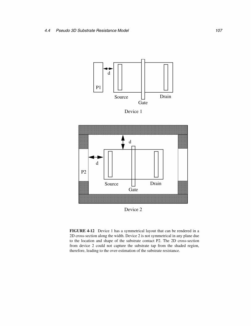
1074.4 Pseudo 3D Substrate Resistance Model
FIGURE 4-12 Device 1 has a symmetrical layout that can be rendered in a2D cross-section along the width. Device 2 is not symmetrical in any plane dueto the location and shape of the substrate contact P2. The 2D cross-sectionfrom device 2 could not capture the substrate tap from the shaded region,therefore, leading to the over-estimation of the substrate resistance.
P1
GateSource Drain
GateSource Drain
P2
Device 1
Device 2
d
d
d
CHAPTER 4 Calibration and Simulation of Substrate Resistance 108
based on device physics− the Rsub0 parameter, representing the bulk resistance before the
snapback, depends on the actual substrate geometry of the device; on the other hand, the
Rd parameter, representing the conductivity modulation by the parasitic bipolar, depends
mainly on the geometry of the intrinsic device (the source, drain, and the channel) that
forms the bipolar transistor. The β of the parasitic bipolar transistor and its conductivity
modulation effect are not influenced by the shape and size of the substrate contacts.
The dependence of Rsub0 on the substrate geometry and the independence of Rd from
the substrate contact can be illustrated by the experimental Isub vs. Id curves obtained from
Devices 1 and 2 as shown in Fig. 4-13. Devices 1 and 2 illustrated in the Fig. 4-12 have
the same intrinsic device, namely the same channel length, source, and drain, but totally
different substrate taps. Examining the two I-I curves, we find that the slope of the curve
during the snapback, which determines Rd, remains roughly the same; its magnitude
changes by about 6%. This shows that 2D QMM simulation method can still be applied to
obtain Rd from a 3D device since the intrinsic lateral bipolar is unaffected by the geometry
of the substrate tap; even the β parameter extracted from the 2D results still remains valid.
However, the y-intercept, which determines the Rsub0 parameter, increases by more than
25% from Device 1 to Device 2, clearly illustrating the impact of changing the substrate
geometry. Changing from the parallel placement (P1) to the enclosed placement (P2)
introduces three additional paths for the substrate current; thus, altering the entire sub-
strate geometry for the device and resulting in a significant reduction of the Rsub0 parame-
ter. Hence, the Rsub0 parameter needs to be modeled using 3D simulation for devices with
a 3D substrate contact geometry.
After realizing that variations the substrate tap geometry moving from 2D to 3D,
only affect the bulk resistivity, adding two more steps to the original QMM method to
model the 3D Rsub0 resistance were shown to be sufficient in forming the Pseudo-3D
QMM model. The two additional steps are two pure resistance simulations to compute the
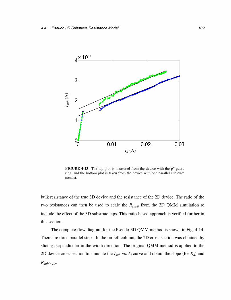
1094.4 Pseudo 3D Substrate Resistance Model
bulk resistance of the true 3D device and the resistance of the 2D device. The ratio of the
two resistances can then be used to scale the Rsub0 from the 2D QMM simulation to
include the effect of the 3D substrate taps. This ratio-based approach is verified further in
this section.
The complete flow diagram for the Pseudo-3D QMM method is shown in Fig. 4-14.
There are three parallel steps. In the far left column, the 2D cross-section was obtained by
slicing perpendicular in the width direction. The original QMM method is applied to the
2D device cross-section to simulate the Isub vs. Id curve and obtain the slope (for Rd) and
Rsub0, 2D.
FIGURE 4-13 The top plot is measured from the device with the p+ guardring, and the bottom plot is taken from the device with one parallel substratecontact.
Id (A)
I sub
(A
)
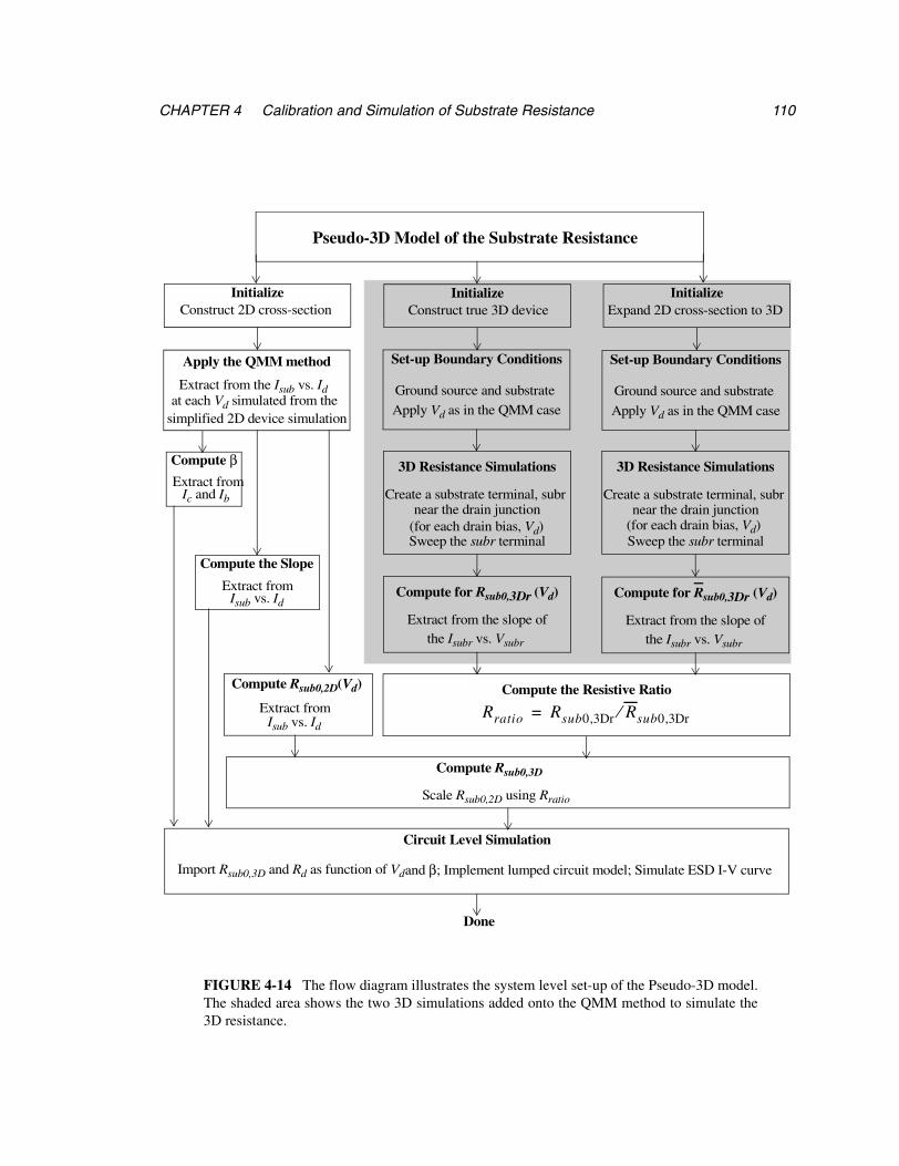
CHAPTER 4 Calibration and Simulation of Substrate Resistance 110
Initialize
Apply the QMM method
Done
Construct 2D cross-section
Extract from the Isub vs. Id at each Vd simulated from the
Circuit Level Simulation
Import Rsub0,3D and Rd as function of Vd
FIGURE 4-14 The flow diagram illustrates the system level set-up of the Pseudo-3D model.The shaded area shows the two 3D simulations added onto the QMM method to simulate the3D resistance.
Extract from
Compute β
and β; Implement lumped circuit model; Simulate ESD I-V curve
Pseudo-3D Model of the Substrate Resistance
Ground source and substrate
Set-up Boundary Conditions
3D Resistance Simulations
Apply Vd as in the QMM case
(for each drain bias, Vd)
Create a substrate terminal, subr
InitializeConstruct true 3D device
InitializeExpand 2D cross-section to 3D
simplified 2D device simulation
Ground source and substrate
Set-up Boundary Conditions
Apply Vd as in the QMM case
near the drain junction
Sweep the subr terminal
3D Resistance Simulations
Create a substrate terminal, subr
near the drain junction
Sweep the subr terminal
Compute for Rsub0,3Dr (Vd)
Extract from the slope of
(for each drain bias, Vd)
the Isubr vs. Vsubr
Compute for Rsub0,3Dr (Vd)
Extract from the slope of
the Isubr vs. Vsubr
Compute the Resistive Ratio
Rratio Rsub0,3Dr Rsub0,3Dr⁄=
Ic and Ib
Extract from
Compute the Slope
Isub vs. Id
Extract from
Compute Rsub0,2D(Vd)
Isub vs. Id
Compute Rsub0,3D
Scale Rsub0,2D using Rratio
1114.4 Pseudo 3D Substrate Resistance Model
The middle and the far right columns are the two 3D pure-resistance simulations for
the ratio-based approach. The true 3D simulation (in the middle column) starts by con-
structing the true 3D device according to the actual layout. Next, proper boundary condi-
tions are applied by grounding the source and substrate terminals while a fixed voltage is
applied to the drain terminal to reverse bias the drain-substrate junction. The applied drain
voltage is the same as in the 2D QMM method so that we can scale the Rsub0,2D (from the
QMM simulation) using the 3D simulation result. A substrate terminal, subr, is artificially
added near the drain junction to emulate the flow path of the generated holes to the sub-
strate contact as shown in Fig. 4-15.1 Finally, a voltage is applied to the subr contact to
start the resistance simulation. The voltage sweep on the subr terminal is stopped before
the p-n junction formed by the substrate and source turns on; the turn-on voltage is usually
around 0.8-0.9V. The 3D substrate resistance, Rsub0, 3Dr can be easily obtained by taking
at each drain bias.
The second 3D simulation in the far right column expands the 2D cross-section
along the width, which is not a true representation of the device geometry. Similar to the
previous 3D simulation, the same boundary conditions and subr terminal are added to the
device. Again, the 3D substrate resistance, Rsub0, 3Dr can be obtained by taking
at each drain bias.
Both extracted 3D resistance Rsub0, 3Dr and Rsub0, 3Dr are simulated under the same
bias conditions, yet there are important differences between the two. The Rsub0, 3Dr models
the true 3D substrate resistance equivalent to the bulk resistance of Device 2 from both the
shaded and unshaded regions in Fig. 4-12. On the other hand, the Rsub0, 3Dr only models
the 3D resistance based on the 2D shape analogous to the unshaded region only in Fig. 4-
12. The ratio of the two resistances, Rratio, can then be used to size Rsub0, 2D accordingly to
1 The #2 black bar in the figure (a) is the location of the subr terminal. The black bars #1 and 3 are used tostudy the dependency of the bulk resistance on the location of the subr later in the section.
Vsubr∆ Isubr∆⁄
Vsubr∆ Isubr∆⁄
CHAPTER 4 Calibration and Simulation of Substrate Resistance 112
include the resistance contribution from the shaded region. The resulting 3D bulk resis-
tance, Rsub0, 3D, can then be multiplied with the slope from the 2D QMM method to yield
Rd. Finally, Rsub0, 3D, Rd, and β can be imported to the compact model for the circuit-level
high-current ESD simulation.
At the first glance, it appears to be more efficient to skip the 3D simulation in the far-
right column by obtaining Rsub0, 3Dr directly from Rsub0, 2D as , where W is
the device width. In reality, scaling the Rsub0, 2D by W restricts the placement of the subr
terminal, forcing it to be the same as the site of hole injection in 2D. Since the hole injec-
tion site bridges the substrate-drain junction, it becomes impossible to reproduce this for
the subr terminal. Furthermore, carrying out the two 3D simulations is advantageous
because the precise location of the subr contact becomes unimportant as long as its loca-
tion is the same in both the true 3D and the expanded 3D structures. This location-inde-
pendent property of the subr terminal for the ratio-based resistance approach needs to be
further verified.
We begin to verify this approach by creating the true 3D structure with P+ guard ring
and the expanded 3D structure with two parallel P+ taps. Then we place the subr terminals
at different locations near the impact ionization site as shown in Fig. 4-15. After extracting
the two resistances, we plot the simulation results in Fig. 4-16. Extracted from the slope of
the Isubr vs. Vsubr curves, the resulting Rsub0, 3Dr (true 3D resistance) and Rsub0, 3Dr (resis-
tance from expanded 2D cross-section) values both increase slightly as the subr terminal
moves closer to the drain terminal. The increase from Location 1 to Location 2 is attrib-
uted to the growing distance to the substrate contact, but the increase from Location 2 to
Location 3 is caused by the bias on the drain terminal. Since both sets of resistance exhibit
the same trends, the resistance ratios, Rratio, are about the same (within 5%) for all three
locations. The same ratio illustrates the advantage of using this approach− the subr termi-
Rsub0,2D W⁄
1134.5 Substrate Resistance Model for Multi-finger Protection Devices
nal can be placed relatively independently of the exact site of impact ionization if it is
placed in the same location in both sets of structures.
With the aid of the Pseudo-3D QMM approach, it is now possible to simulate the
substrate resistances from layouts with various 3D substrate geometries. We can apply this
method to capture the substrate coupling effects between the device elements.
4.5 SUBSTRATE RESISTANCE MODEL FOR MULTI-FINGER
PROTECTION DEVICES
To this point, only single-finger ESD protection devices have been modeled. How-
ever, the protection offered by such a single-finger device is insufficient to pass the ESD
robustness standard. The obvious solution is to use multi-finger protection devices, adding
up the current-carrying capabilities from each finger to boost the ESD robustness.1 Ide-
ally, the ESD robustness would be scaled up by the number of fingers as
. However, it is well documented that not all fingers turn-on at
the same time during ESD stress [82,83]. Typically a few fingers break down first and
snap back to a lower voltage, while the remaining fingers will not have a chance to turn-
on. As a result, multi-finger protection devices offer a lower level of protection than is
implied by the physical number of fingers used.
This type of a non-uniform turn-on behavior can be counteracted using circuit design
techniques. Gate bounce is one such technique [14]. Simple RC circuits are used to couple
part of the stress voltage to the gate in order to reduce the trigger voltage; this eliminates
the non-uniform turn-on problem. However, for high-speed circuits, when the rise time of
the ESD stress waveform is slower than the regular input waveform, the gate bounce tech-
1 The ESD robustness standards are briefly mentioned on page 12 of Chapter 2. Please refer to [1,2,4,8,41]for detailed descriptions.
KV finger⁄ # of fingers⋅
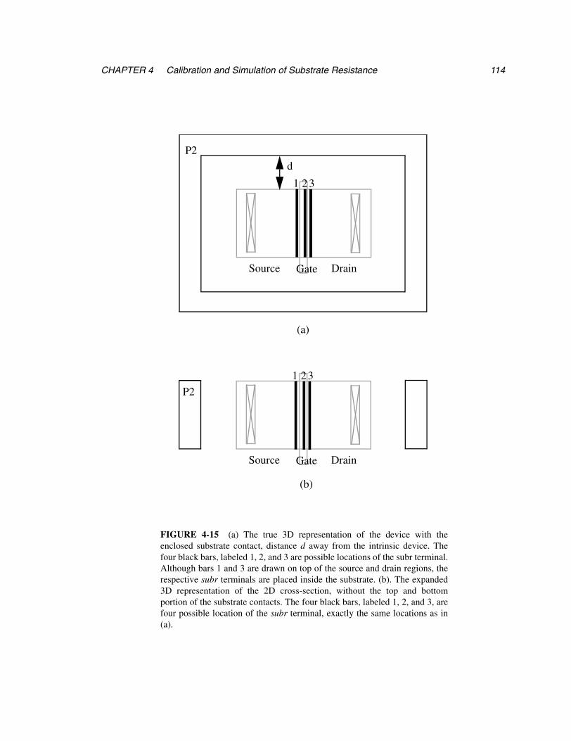
CHAPTER 4 Calibration and Simulation of Substrate Resistance 114
GateSource Drain
P2d
1 2 3
(a)
GateSource Drain
P2
(b)
FIGURE 4-15 (a) The true 3D representation of the device with theenclosed substrate contact, distance d away from the intrinsic device. Thefour black bars, labeled 1, 2, and 3 are possible locations of the subr terminal.Although bars 1 and 3 are drawn on top of the source and drain regions, therespective subr terminals are placed inside the substrate. (b). The expanded3D representation of the 2D cross-section, without the top and bottomportion of the substrate contacts. The four black bars, labeled 1, 2, and 3, arefour possible location of the subr terminal, exactly the same locations as in(a).
1 2 3

1154.5 Substrate Resistance Model for Multi-finger Protection Devices
nique cannot be used to prevent the activation of the ESD circuit during normal operation.
Adding drain resistance to each finger is another technique to improve turn-on uniformity
[82]. The drain resistance can increase the drain bias after snapback, helping the additional
fingers to turn on. However, the extra drain resistance can decrease the protection level
from the negative ESD stress1 by increasing the substrate-drain diode’s turn-on voltage.
Furthermore, even if each finger breaks down at the same time, the non-uniform
behavior among the fingers can still occur due to the varying substrate resistance associ-
ated with each finger. The fingers with larger substrate resistance can cause the associated
lateral bipolar transistors to turn on earlier at a lower substrate current. Hence, they would
go to a low impedance state sinking all of the stress current, preventing other fingers from
turning on, and reducing the ESD robustness of the protection element. Experimentally, it
is impossible to measure the magnitude of the substrate resistance for each finger on a
multi-finger device without designing test structures beforehand. Therefore, the Pseudo-
3D QMM method becomes particularly useful in simulating the substrate resistance asso-
ciated with each finger so that the ESD protection level with a given multi-finger structure
can be accurately estimated.
As shown in Fig. 4-17, the six-fingered2 nMOS device surrounded by a p+ tap ring is
a commonly used ESD protection device. The guard ring shaped substrate contact is
widely used in industry to prevent latch up during normal operation and to prevent any
ESD current from flowing into the substrate of the core circuitry. Clearly from the layout,
the single-fingered nMOS devices on the far left and far right have the smallest substrate
resistance due to their physical proximity to the substrate tap. However, the quantitative
difference of substrate resistance associated with each finger is not known. As a result, the
protection level offered by this multi-fingered structure is equally unclear even if all the
1 The negative stress means that the stress is positive from ground to the pad. Under a negative stress, thenMOS protection device behaves like a simple pn diode, formed by the substrate to drain junction.
2 The six-fingered count is obtained by counting the number of gates.

CHAPTER 4 Calibration and Simulation of Substrate Resistance 116
FIGURE 4-16 (a) Rsub0, 3Dr and Rsub0, 3Dr vs. each subr location as labeled in the
previous figure. In both cases, the resistance value increases as the subr terminalapproaches the drain. (b) Rratio between the two resistors remains constant,independent of the distance between the subr terminal and the impact ionization site.
Subr Terminal Location (#)
Res
ista
nce
(Ω)
(a)
Subr Terminal Location (#)
Rra
tio
(b)
Rsub0, 3Dr (from true 3D device)
Rsub0, 3Dr
Rsub0, 3Dr----------------------
Rsub0, 3Dr (from expanded 2D cross-section)
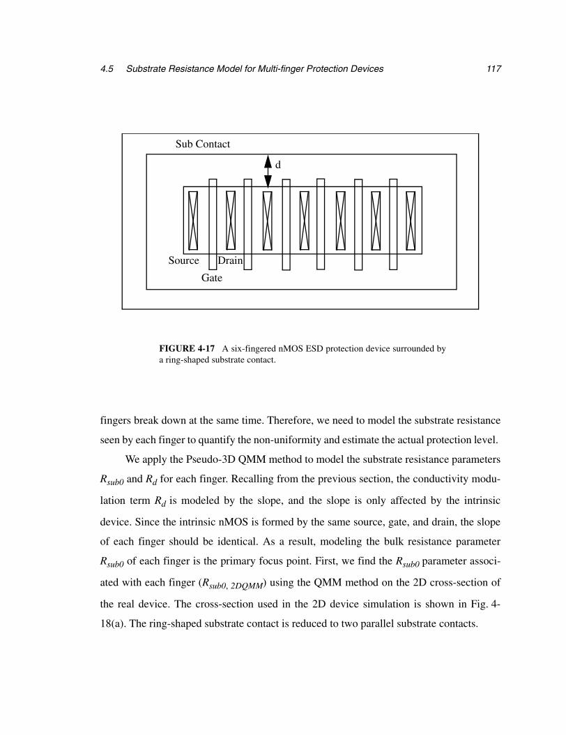
1174.5 Substrate Resistance Model for Multi-finger Protection Devices
fingers break down at the same time. Therefore, we need to model the substrate resistance
seen by each finger to quantify the non-uniformity and estimate the actual protection level.
We apply the Pseudo-3D QMM method to model the substrate resistance parameters
Rsub0 and Rd for each finger. Recalling from the previous section, the conductivity modu-
lation term Rd is modeled by the slope, and the slope is only affected by the intrinsic
device. Since the intrinsic nMOS is formed by the same source, gate, and drain, the slope
of each finger should be identical. As a result, modeling the bulk resistance parameter
Rsub0 of each finger is the primary focus point. First, we find the Rsub0 parameter associ-
ated with each finger (Rsub0, 2DQMM) using the QMM method on the 2D cross-section of
the real device. The cross-section used in the 2D device simulation is shown in Fig. 4-
18(a). The ring-shaped substrate contact is reduced to two parallel substrate contacts.
Gate
Source Drain
Sub Contact
d
FIGURE 4-17 A six-fingered nMOS ESD protection device surrounded bya ring-shaped substrate contact.
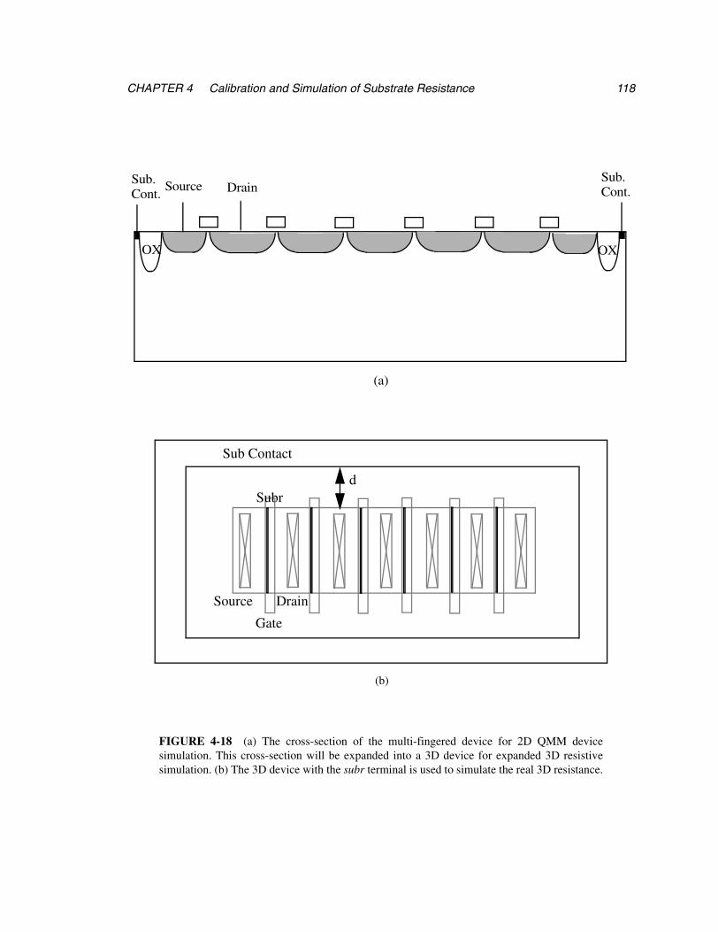
CHAPTER 4 Calibration and Simulation of Substrate Resistance 118
OX OX
Sub.Cont.
Sub.Cont.Source Drain
(a)
Gate
Source Drain
Sub Contact
dSubr
FIGURE 4-18 (a) The cross-section of the multi-fingered device for 2D QMM devicesimulation. This cross-section will be expanded into a 3D device for expanded 3D resistivesimulation. (b) The 3D device with the subr terminal is used to simulate the real 3D resistance.
(b)

1194.5 Substrate Resistance Model for Multi-finger Protection Devices
Since the Rsub0, 2DQMM does not capture the effect of the ring-shaped substrate tap,
two additional simulations are needed. The first resistive simulation involves obtaining the
substrate resistance Rsub0, 3Dr for each finger from the three-dimensional device in Fig. 4-
18(b). This device is identical to the real multi-fingered device in Fig. 4-17, except for the
artificially placed contact, subr. The second resistive simulation involves finding the sub-
strate resistance Rsub0, 3Dr for each finger from the expanded 2D device (along the width
direction) in Fig. 4-18(a). The subr contacts are placed in the same location as the previ-
ous simulation.
The Rsub0, 2DQMM, Rsub0, 3Dr, and Rsub0, 3Dr for each finger are plotted in Fig. 4-
19(a), (b), and (c) respectively. After scaling the Rsub0, 2DQMM using the ratio from
, the resulting spread of Rsub0 for each finger is graphed in Fig. 4-20.
In the above plots, the finger numbers 1-6 are assigned in the left-to-right order.
The same trend is observed in all four simulation results. In Fig. 4-19 and Fig. 4-20,
mirror symmetry between the fingers is observed, namely the pair of fingers 1 and 6, 2 and
5, 3 and 4 have the same resistive values. This symmetry stems from the symmetry in the
geometry of the device−the pair of fingers are equal distance away from the substrate con-
tact. The distance of each finger to the substrate tap can also explain the decreasing resis-
tance from the center fingers (3 and 4) to the side fingers (1 and 6). Clearly, fingers 1 and
6 are the closest to the p+ tap, thus, possessing the lowest substrate resistance. Fingers 3
and 4 are the furthest from the guard ring, therefore, exhibiting the highest substrate resis-
tance. The resistance drops from finger 3 to 1 in an exponential manner. This illustrates
that the substrate current flows toward the surface for fingers 1 and 6, and shifts deeper
toward the p+ part of the substrate as the device moves further away as explained earlier in
Section 4.2.
Although the general trend is the same for two type of substrate contacts, there are
still three major differences. First, the magnitude of the resistance values for all of the fin-
Rsub0, 3Dr Rsub0,3Dr⁄
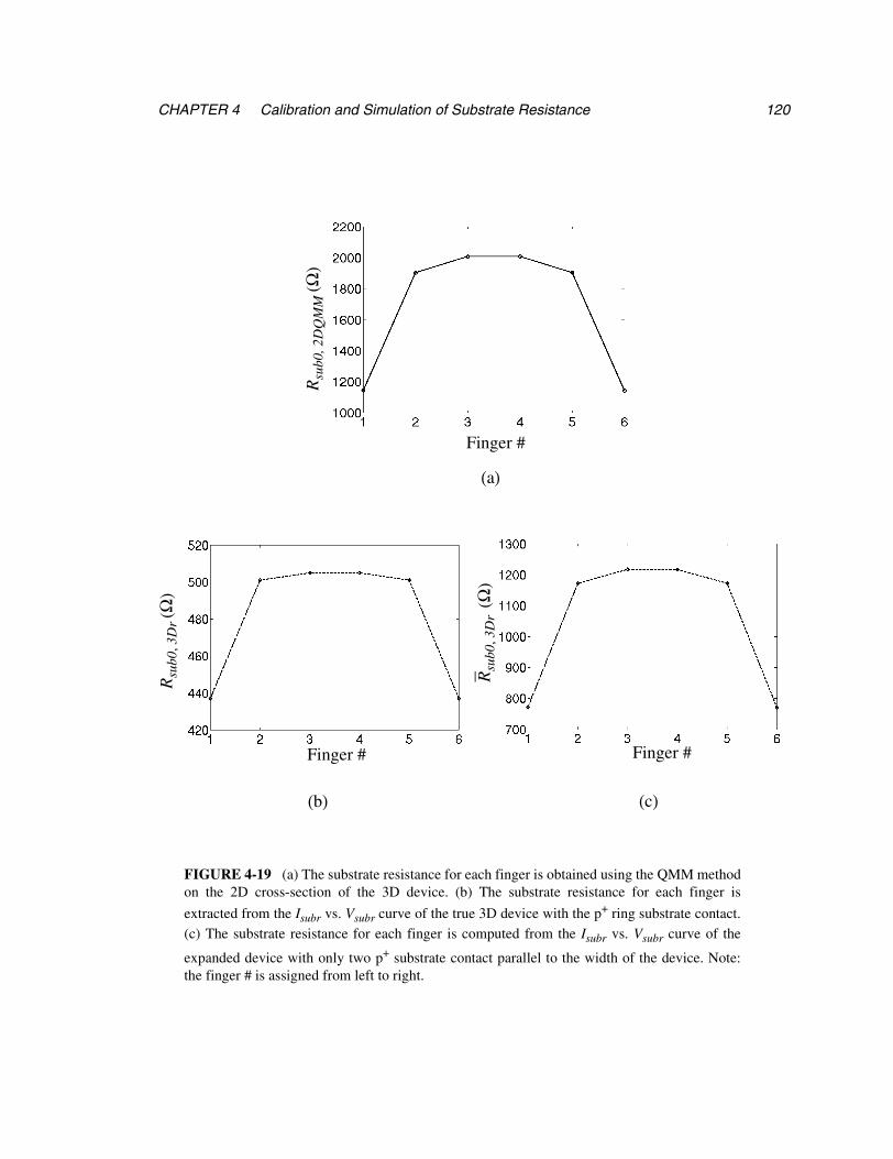
CHAPTER 4 Calibration and Simulation of Substrate Resistance 120
Finger #
Rsu
b0, 2
DQ
MM
(Ω)
(a)
Finger # Finger #
Rsu
b0, 3
Dr
(Ω)
Rsu
b0, 3
Dr
(Ω)
(b) (c)
FIGURE 4-19 (a) The substrate resistance for each finger is obtained using the QMM methodon the 2D cross-section of the 3D device. (b) The substrate resistance for each finger is
extracted from the Isubr vs. Vsubr curve of the true 3D device with the p+ ring substrate contact.(c) The substrate resistance for each finger is computed from the Isubr vs. Vsubr curve of the
expanded device with only two p+ substrate contact parallel to the width of the device. Note:the finger # is assigned from left to right.
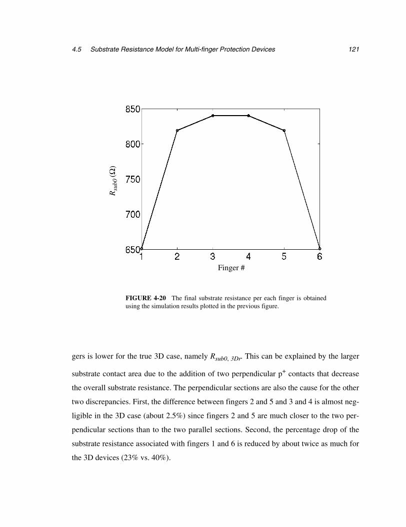
1214.5 Substrate Resistance Model for Multi-finger Protection Devices
gers is lower for the true 3D case, namely Rsub0, 3Dr. This can be explained by the larger
substrate contact area due to the addition of two perpendicular p+ contacts that decrease
the overall substrate resistance. The perpendicular sections are also the cause for the other
two discrepancies. First, the difference between fingers 2 and 5 and 3 and 4 is almost neg-
ligible in the 3D case (about 2.5%) since fingers 2 and 5 are much closer to the two per-
pendicular sections than to the two parallel sections. Second, the percentage drop of the
substrate resistance associated with fingers 1 and 6 is reduced by about twice as much for
the 3D devices (23% vs. 40%).
Finger #
Rsu
b0 (Ω
)
FIGURE 4-20 The final substrate resistance per each finger is obtainedusing the simulation results plotted in the previous figure.
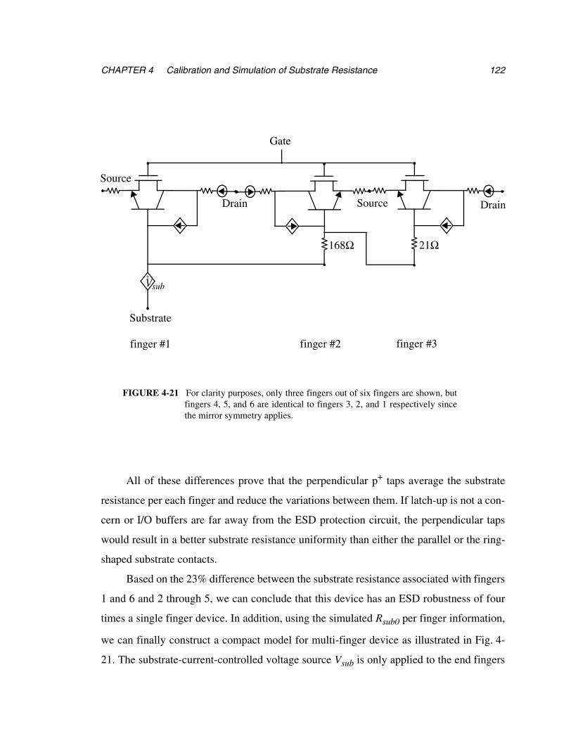
CHAPTER 4 Calibration and Simulation of Substrate Resistance 122
All of these differences prove that the perpendicular p+ taps average the substrate
resistance per each finger and reduce the variations between them. If latch-up is not a con-
cern or I/O buffers are far away from the ESD protection circuit, the perpendicular taps
would result in a better substrate resistance uniformity than either the parallel or the ring-
shaped substrate contacts.
Based on the 23% difference between the substrate resistance associated with fingers
1 and 6 and 2 through 5, we can conclude that this device has an ESD robustness of four
times a single finger device. In addition, using the simulated Rsub0 per finger information,
we can finally construct a compact model for multi-finger device as illustrated in Fig. 4-
21. The substrate-current-controlled voltage source Vsub is only applied to the end fingers
Vsub
Substrate
+
-
FIGURE 4-21 For clarity purposes, only three fingers out of six fingers are shown, butfingers 4, 5, and 6 are identical to fingers 3, 2, and 1 respectively sincethe mirror symmetry applies.
Source
Drain
Gate
DrainSource
finger #1 finger #2 finger #3
168Ω 21Ω
1234.5 Substrate Resistance Model for Multi-finger Protection Devices
1 and 6, with Rsub0 of 651Ω. In addition to sharing Vsub with fingers 1 and 6, fingers 2
through 5 also have additional substrate resistance, resulting from the difference between
the substrate resistances.
This multi-finger compact model captures the interaction between each finger via
the substrate, demonstrating the power of the Pseudo-3D QMM method. Using simple
resistance simulations coupled with the 2D QMM approach, we were able to simulate sub-
strate coupling effects, which previously could only be modeled using experimental
means.

CHAPTER 4 Calibration and Simulation of Substrate Resistance 124
CHAPTER 5
CONCLUSIONS AND FUTURE WORK
5.1 CONTRIBUTIONS
Protecting ICs against ESD damage becomes an uphill battle as the critical device
dimensions continue to shrink and design cycles are shortened. The core of the on-chip
ESD protection is the protection device itself. For a given technology, the protection
device’s electrical and thermal characteristics depend on its geometry and layout. In order
to find the optimal device geometry, test structures are designed and then measured across
a set of layout variations. To avoid this costly and time consuming trial-and-error
approach, simulation must be used to accurately model the protection devices, thus, offer-
ing an explanation of the underlying physics and narrowing the range of test structures to
be explored experimentally. This chapter reviews the thesis contribution toward develop-
ing and implementing such a modeling methodology, and delineates future work in the
area of ESD protection circuit modeling.
124
CHAPTER 5 Conclusions and Future Work 125
In this dissertation, a novel methodology was formulated and implemented−the
Pseudo-3D Quasi-Mixed-Mode−for modeling and characterizing ESD protection devices
with process and layout variations. This methodology focuses on modeling the substrate
resistance in the deep submicron CMOS technology. By accurately simulating the sub-
strate resistance, this approach brings layout-dependent modeling into the ESD circuit
simulation. The P-3D QMM methodology consists of three different types of models: the
compact ESD circuit model, the 2D Quasi-Mixed-Mode approach, and finally the 3D
resistance scaling method. The contributions of each model are briefly highlighted.
The compact ESD circuit model. After reviewing the existing ESD analytical
models, the circuit model created by Ameraskera et. al. was selected based on its simplic-
ity and physics-based implementation as well as demonstrated good agreement with
experimental data. Most importantly, this circuit model was chosen because it was the
only model to simulate the conductivity-modulated aspect of the substrate resistance
under ESD stress.
The scope of the substrate resistance model was extended to include the effect of
drain resistance for silicide-blocked devices, which are widely used for ESD protection. A
graphical impact ionization parameter (M parameter) extraction method was also used
since the original method uses only a few data points for extraction. The graphical method
uses all available data points before the snapback region of operation to ensure that the
extracted M parameters fit the experimental data globally.
The complete model was successfully implemented into the widely used commercial
circuit simulator Hspice, including a model formulation that helps to overcome conver-
gence issues. The initial convergence problem was solved by modifying the avalanche
breakdown equation in the conventional device model. Prior to this work, convergence
issues were typically solved by porting the circuit models into in-house circuit models or
by changing the source code of the simulator itself. Enhanced portability and versatility of
the new circuit model have been achieved by implementing it inside a standard (commer-
5.1 Contributions 126
cial) simulator without modifying the source code. As a result, accurately simulation of
the high-current characteristics of a device under the ESD stress were achieved. Good
agreement between the simulated results and experimental data verified the accuracy of
the extended substrate resistance model and the new M extraction method.
The 2D Quasi-Mixed-Mode Method. Previous compact models lacked layout-
dependent modeling capabilities because the substrate resistance once extracted, becomes
a fixed set of parameters that do not scale with device geometry. To overcome this limita-
tion, a substrate resistance model was developed that scales with layout. There are existing
methods to model the layout geometry, but all require a large number of test structures.
Therefore, this work concentrated on developing simulation approaches that only need a
few test structures for calibration.
Our new methodology, the Quasi-Mixed-Mode (QMM) device and circuit simula-
tion, achieves the desired goals. The QMM model enables the simulation of different lay-
out and process variations by focusing on modeling the substrate region. Device
simulation was used to compute the substrate’s process and layout dependencies from the
2D cross-section of a device containing technology and geometry information. The sub-
strate resistance parameters are then extracted from the output of the device simulation
and imported into the circuit simulation. The calibration procedure was improved as well
as convergence robustness, and computational efficiency of the device simulation, making
it possible to use device simulations to compute substrate resistances for a large number of
devices. The improvement is achieved by using the simplified device simulation, which
uses manual hole injection to emulate avalanche hole generation. This hole injection
method was inspired by an unrelated but powerful simulation approach that is used for
simulating photo generation processes.
The QMM approach was also applied to model deep submicron nMOSFETs with
layout and process variations based on state-of-the-art fabrication technology. Good
agreement between the simulation results and the experimental data demonstrates the
CHAPTER 5 Conclusions and Future Work 127
model’s accuracy in capturing the quantitative trends as the device geometry varies. In
addition, analysis helps to explain the quantitative trends for different current and voltage
conditions derived from the model.
The Pseudo-3D QMM Methodology. The 2D cross-section in the QMM approach
limits the modeling to 3D devices that are symmetrical in the z-direction (the width direc-
tion). Devices with a ring-shaped substrate contact represent one such case. The 2D QMM
method also cannot model the three-dimensional interactions between device elements
through the common substrate. The variations between the substrate resistance of each fin-
ger inside the multi-fingered device is an example.
The Pseudo-3D QMM methodology improves upon the 2D QMM approach by
developing a 3D substrate resistance model. The key step in the P-3D QMM method is to
use the 3D resistance ratio to scale the substrate resistance parameters obtained from the
2D QMM approach. The ratio is formed by two substrate resistances, which are extracted
from two different 3D resistance simulations. The numerator resistance is simulated using
the substrate of the true 3D device, and the denominator resistance is simulated using the
substrate of the expanded 2D device (expanded by the width). The ratio captures the 3D
resistance effects. In the best case, 3D device simulations are extremely slow; in the worst
case, they never converge. However with the 3D device simulations, the computational
speed and robustness, achieved in the 2D QMM method, can still be maintained since only
3D resistance simulations are used.
Aside from being able to model the substrate resistance of any device, the P-3D
QMM approach’s true power lies in its ability to model the substrate coupling effects
between devices, especially since the coupling effects are very difficult to determine
experimentally. In the case of the widely-used multi-fingered protection device, it is very
useful to know the variations between the substrate resistance for each finger because the
uniformity is essential for a robust ESD protection. Without specially designed test struc-
tures, the substrate resistance per finger cannot be measured. The P-3D QMM approach
5.2 Suggested Future Work 128
was applied to model the individual substrate resistance associated with each finger. From
the various resistance values, the number of fingers could be estimated that would turn on
under the ESD stress; hence, the real protection power offered by this multi-finger device
can also be evaluated. By simulating the substrate resistance per finger for different types
of substrate contacts, the P-3D QMM method offers insight into the optimal shape of add-
ing substrate contacts.
The methodology of combining the device and circuit simulation, using device sim-
ulation for modeling geometry-dependent parameters and circuit simulation for technol-
ogy-dependent parameters, is the major contribution of this dissertation.
5.2 SUGGESTED FUTURE WORK
This thesis offers four different branches for further research in the area of ESD
device and circuit modeling.
Application of the P-3D QMM method. Since nMOSFETs are usually the weakest
devices under the ESD stress, the dissertation has focused on modeling the nMOS. The
other devices frequently used for ESD protection, such as the bipolar transistor and diode,
were not discussed. However, the P-3D QMM methodology is general enough to be
applied to the other devices as well. For example, since the junction breakdown mecha-
nisms of these other active devices are very similar to that of the nMOS, the analytical
nMOS impact ionization model can be used with a few changes. Similarly, the resistance
associated with each device can also be modeled using the QMM method by constructing
the geometric shape along with the technology information in the device simulator.
Modeling the interaction of the circuits through a common substrate. Properly
designed protection circuits conduct the stress current away from the core by providing
the lowest impedance path during the ESD stress event. Often, when there is a lower
impedance path through the internal circuit, the stress current will flow in that direction,
CHAPTER 5 Conclusions and Future Work 129
causing damage to the internal circuit. Using the 3D resistance simulation method, an
extended block of the substrate can be reduced to a network of substrate resistance ele-
ments. When this network of resistance elements is ported into the circuit simulator, along
with the circuitry, the interactions of the circuit elements through the common substrate
can also be modeled. Furthermore, the 3D resistive simulation method can be used to
study the substrate noise coupled from the digital circuits to the analog circuit.
Modeling substrate pumping. Recently, Oh et. al. observed the non-uniform bipo-
lar conduction phenomenon for silicided single-finger nMOS in deep-submicron technol-
ogy [80]. This non-uniformity severely degrades the ESD robustness of the silicided
device, and it is particularly severe for silicided devices under 0.15µm. Silicide-blocked
devices with nominal width do not (yet) have this problem. Oh further noted that by apply-
ing positive bias to the substrate contact the bipolar conduction uniformity can be
improved. In order to bias the substrate contact during the ESD stress event, the substrate
pump circuits are designed to inject substrate current into the substrate. This current injec-
tion scheme changes the substrate resistance model described in this thesis. The hole
injection technique used in the QMM approach can be used to study the effect of the cur-
rent injection and in turn to formulate a new substrate model.
Electrical-thermal circuit model. In this thesis, only the electrical characteristics of
the protection devices has been modeled. Although a few empirical observations can be
made about a device’s thermal robustness from the electrical characteristics, a thermal
model is needed to quantitatively compare the ESD robustness of protection devices with
process and layout variations. The current and voltage information from the P-3D QMM
model can be taken as an accurate electrical basis to begin the electro-thermal simulation,
aiding in thermal modeling.
BIBLIOGRAPHY
[1] A. Ameraskera and C. Duvvury, ESD in Silicon Integrated Circuits, John Wiley &
Sons Ltd, West Sussex, England, 1995.[2] S. Dabral and T. Maloney, Basic ESD and I/O Design, John Wiley & Sons, Inc.,New York, 1998.
[3] O. J. McAteer, “An effective ESD awareness training program,” Proc. 1st EOS/ESDSymposium, pp. 1-3, 1979.
[4] S. Beebe, “Characterization, Modeling and Design of ESD Protection Circuits,”PhD Thesis, Stanford University, 1998.
[5] T. Green and W. Denson, “A Review of EOS/ESD field failures in military equip-ment,” Proc. 10th EOS/ESD Symposium, pp. 7-14, 1988.
[6] C. Diaz, C. Duvvury, S.-M. Kang, and L. Wagner, “Electrical overstress (EOS)power profiles: A guideline to qualify EOS hardness of semiconductor devices,”Proc. 14th EOS/ESD Symposium, pp. 88-94, 1992.
[7] R. Merrill and E. Issaq, “ESD design methodology,” Proc. 15th EOS/ESD Sympo-sium, pp. 233-237, 1993.
[8] S. Ramaswamy, “Modeling Simulation and Design Guidelines for EOS/ESD Pro-tection Circuits in CMOS Technologies,” PhD Thesis, University of Illinois atUrbana-Champaign, 1996.
130

Bibliography 131
[9] C. Duvvury, R. Rountree, and R. McPhee, “ESD Protection: design and layoutissues for VLSI circuits,” IEEE Transactions on Industry Applications, vol. 25, no.1, pp. 41-47, 1989.
[10] C. Duvvury and A. Amerasekera, “ESD: A pervasive reliability concern for ICtechnologies,” Proc. of the IEEE, vol. 81, no. 5, pp. 690-702, 1993.
[11] K. L. Chen, “Effect of Interconnect Process and Snapback Voltage on the ESDFailure Threshold of NMOS Transistors,” Proc. 10th EOS/ESD Symposium, pp.212-219, 1988.
[12] T. Polgreen, A. Chatterjee, “Improving the ESD Failure Threshold of SilicidednMOS Output Transistors by Ensuring Uniform Current Flow,” Proc. 11th EOS/ESD Symposium, pp. 182-189, 1989.
[13] C. Duvvury and C. Diaz, “Dynamic Gate Coupling of NMOS for Efficient OutputESD Protection,” Proc. IEEE International Reliability Physics Symposium, pp.141-150, 1992.
[14] J. Chen, A. Amerasekera, C. Duvvury, “Design Methodology and Optimization ofGate Driven NMOS ESD Protection Circuits In Submicron CMOS Process,” IEEETransactions Electron Devices, vol. ED-45, pp. 2448-2456, 1998.
[15] A. Chatterjee, T. Polgreen, and A. Amerasekera, “A Low-Voltage Triggering SCRfor On-Chip Protection at Output and Input Pads,” Electron Device Letter, EDL-12,pp. 21-22, 1991.
[16] C. Diaz and G. Motley, “Bi-Modal Triggering for LVSCR ESD ProtectionDevices,” Proc. 16th EOS/ESD Symposium, pp. 106-112, 1994.
[17] K. Kreiger, “Novel NMOS Triggering for SCR ESD Protection Devices,” Proc.23rd EOS/ESD Symposium, pp. 51-56, 2001.
[18] T. J. Maloney and S. Dabral, “Noval Clamp Circuit for IC Power Supply Protec-tion,” Proc. EOS/ESD Symposium, pp. 1-6, 1995.
[19] C. Duvvury, S. Ramaswamy, A. Amerasekera, R. Cline, B. Andresen, and V.Gupta, “Substrate Pump NMOS for ESD Protection Applications,” Proc. 22ndEOS/ESD Symposium, pp. 7-11, 2000.

132 Bibliography
[20] C. Salling, J. Hu, J. Wu, C. Duvvury, R. Cline, and R. Pok, “Development of Sub-strate-Pumped nMOS Protection for a 0.13µm technology,” Proc. 23rd EOS/ESDSymposium, pp. 12-17, 2001.
[21] B. Kleveland, T. Maloney, J. Morgan, L. Madden, T. H. Lee, and S. S. Wong, “Dis-tributed ESD Protection for High-speed Integrated Circuits,” IEEE Electron DeviceLetters, vol. 21, pp. 390-392, 2000.
[22] D. L. Lin, “ESD Sensitivity and VLSI Technology Trends: Thermal Breakdownand Dielectric Breakdown,” Proc. 15th EOS/ESD Symposium, pp. 73-81, 1993.
[23] S. H. Voldman and V. P. Gross, “Scaling, Optimization and Design Considerationsof Electrostatic Discharge Protection Circuits in CMOS Technology,” Proc. 15thEOS/ESD Symposium, pp. 251-260, 1993.
[24] A. Chatterjee, T. Polgreen, and A. Amerasekera, “Design and Simulation of a 4 kVESD Protection Circuit for 0.8µm BiCMOS Process”, Proc. International ElectronDevice Meeting, pp. 913-916, 1991.
[25] C. Diaz, C. Duvvury, and S. M. Kang, “Studies of EOS Susceptibility in 0.6µmnMOS/ESD I/O Protection Structures,” Proc. 15th EOS/ESD Symposium, pp. 83-91, 1993.
[26] A. Amerasekera, A. Chatterjee, and M. C. Chang, “Prediction of ESD Robustnessin a Process Using 2-D Device Simulations,” Proc. IEEE International ReliabilityPhysics Symposium, pp. 161-167, 1993.
[27] A. Amerasekera, M.C. Chang, J. Seitchik, A. Chatterjee, K. Mayaram, and J.H.Chern, “Self-Heating Effects in Basic Semiconductor Structures”, IEEE Transac-tions on Electron Devices, ED-40, pp. 1836-1844, 1993.
[28] P. Yang and J.H. Chern, “Design for Reliability: The Major Challenge for VLSI,”Proc. of IEEE, vol. 81, pp. 730-744, 1993.
[29] A. Amerasekera, S. Ramaswamy, M.C. Chang, and C. duvvury, “Modeling MOSSnapback and Parasitic Bipolar Action for Circuit-Level ESD and High CurrentSimulations”, IEEE International Reliability Physics Symposium, pp. 318-326,1996.

Bibliography 133
[30] C. Diaz, “Modeling and Simulation of Electrical Overstress Failures in Input/Out-put Protection Devices of Integrated Circuits,” PhD Thesis, University of Illinois atUrbana-Champaign, 1993.
[31] C. Diaz, “Electrothermal Simulation of Electrical Overstress in Advanced nMOSESD I/O Protection Circuits,” Proc. International Electron Device Meeting, pp.899-902, 1993.
[32] R. A. M. Beltman, H. van der Vlist, and A. J. Mouthaan, “Simulation of ThermalRunaway during ESD Events,” Proc. 12th EOS/ESD Symposium, pp. 157-161,1990.
[33] K. Kurimoto, K. Yamashita, I. Miyanaga, A. Hori, and S. Odanaka, “An Electro-thermal Circuit Simulation using an Equivalent Thermal Network for ElectrostaticDischarge,” Proc. VLSI Symposium on Technology, pp. 127-128, 1994.
[34] S. Ramaswamy, A. Amerasekera, and M.C. Chang, “A Unified Substrate CurrentModel for Weak and Strong Impact Ionization in sub-0.25µm NMOS Devices,”Proc. International Electron Device Meeting, pp. 885-888, 1997.
[35] F. Hsu, P. Ko, S. Tam, C. Hu, and R. Muller, “An Analytical Breakdown Model forShort-Channel MOSFET’s,” IEEE Transactions on Electron Devices, vol. ED-29,pp.1735-1740, 1982.
[36] M. Mergens, W. Wilkening, S. Mettler, H. Wolf, and W. Fichtner, “ModularApproach of a High Current MOS Compact Model for Circuit-level ESD Simula-tion Including Transient Gate Coupling Behavior,” Proc. IEEE International Reli-ability Physics Symposium, pp. 167-178, 1999.
[37] T. Skotnicki, G. Merckel, and A. Merrachi, “New Physical Model of Multiplica-tion-Induced Breakdown in MOSFETs,” Solid State Electronics, vol. 34, pp.1297-1307, 1991.
[38] T. Li, T. Tsai, E. Rosenbaum, and S. kang, “Substrate Resistance Model for Simu-lating MOSFET Breakdown in ESD Protection,” Techcon, 1998.
[39] R.J.G. Goossens, S. Beebe, Z. Yu, and R. W. Dutton, “An Automatic BiasingScheme for Tracing Arbitrarily Shaped I-V Curves,” IEEE Transaction Computer-Aided Design, vol. CAD-13, pp.310-317, 1994.
134 Bibliography
[40] “MEDICI Two-Dimensional Semiconductor Device Simulation, Version 2.1”,Technology Modeling Associates, Inc., Sunnyvale, CA, 1997.
[41] “MIL STD 883.C/3015.7 notice 8,” Military Standard for Test Methods and Proce-dures for Microelectronics: ESD Sensitivity Classification, March 22, 1989.
[42] L. J.Van Roozendaal, A. Amerasekera, P. Bos, W. Baelde, F. bontekoe, P. Kersten,E. Korma, P. Rommers, P. Krys, U. Weber, and P. Ashby, “Standard ESD Testing,”Proc. 12th EOS/ESD Symposium, pp. 119-130, 1990.
[43] D. L. Lin and T. L. Welsher, “From Lightning to Charged-Device Model Electro-static Discharges,” Proc. 14th EOS/ESD Symposium, pp. 68-75, 1992.
[44] N. Khurana and T. Maloney, and W. Yeh, “ESD on CMOS Devices-- EquivalentCircuits, Physical Models and Failure Mechanisms,” Proc. IEEE InternationalReliability Physics Symposium, pp. 212-223, 1985.
[45] T. Maloney and N. Khurana, “Transmission Line Pulsing Techniques for CircuitModeling of ESD Phenomena,” Proc. 8th EOS/ESD Symposium, pp. 49-54, 1985.
[46] D. G. Pierce, W. Shiley, B. D. Mulcahy, K. E. Wagner, and M. Wunder, “ElectricalOverstress Testing of a 256K UVEPROM to Rectangular and Double ExponentialPulses,” Proc. 10th EOS/ESD Symposium, pp. 137-146, 1988.
[47] A. Amerasekera, L. van Roozendal, J. Bruines, and F. Kuper, “Characterizationand Modeling of Second Breakdown in NMOSTs for the Extraction of ESD-Related Process and Design Parameters,” IEEE Transactions on Electron Devices,vol. ED-38, pp. 2161-2168, 1991.
[48] R. Muller and T. Kamins, Device Electronics for Integrated Circuits, John Wiley &Sons, New York, USA, 1986.
[49] D. P. Kennedy and A. Phillips, Jr., “Source-Drain Breakdown in an Insulated GateField-Effect Transistor,” Proc. International Electron Device Meeting, pp. 160-165,1973.
[50] T. Toyabe, K. Yamaguchi, S. Asai, and M. Mock, “A Numerical Model of Ava-lanche Breakdown in MOSFET’s,” IEEE Transactions on Electron Devices, vol.ED-25, pp. 825-832, 1978.

Bibliography 135
[51] E. Sun, J. Moll, J. Berger, and B. Alders, “Breakdown Mechanism in Short-Chan-nel MOS Transistors,” Proc. International Electron Device Meeting, pp. 478-482,1978.
[52] P. K. Ko, R. S. Muller, and C. Hu, “A Unified Model for Hot-Electron Currents inMOSFETs,” Proc. International Electron Device Meeting, pp. 600-603, 1981.
[53] A. Amerasekera and J. Seitchik, “Electrothermal Behavior of Deep SubmicronnMOS Transistors Under High Current Snapback (ESD/EOS) Conditions,” Proc.International Electron Device Meeting, pp.455-458, 1994.
[54] S. M. Sze, Physics of Semiconductor Devices, John Wiley & Sons, New York,1969.
[55] N. Aurora, M. S. Mahesh, and S. Sharma, “MOSFET Substrate Current Model forCircuit Simulation,” IEEE Transactions on Electron Devices, vol. 38, pp.1392-1398, 1991.
[56] C. Hu, “Hot Carrier Effects,” Advanced MOS Device Physics, N. G. Einspruch andG. Gildenblat, Eds., New York, 1989.
[57] Y. Okuto and C. Crowell, “Threshold Energy Effect on Avalanche BreakdownVoltage in Semiconductor Junctions,” Solid-State Electronics, Vol. 18, pp.161-168,1975.
[58] BSIM3 User’s Manual, Berkeley, 1993.
[59] W. Y. Jang, C. Y, Wu, and H. J. Wu, “A New Experimental Method to Determinethe Saturation Voltage of a Small-Geometry MOSFET,” Solid-State Electron, vol.31, pp.1421-1431, 1988.
[60] T. Y. Chan, P. K. Ko, and C. Hu, “A Simple Method to Characterize Substrate Cur-rent in MOSFET’s,” IEEE Electron Device Letter, vol. 5, pp.505-507, 1984.
[61] X. Y. Zhang, Z. Yu, S. Beebe, and R. W. Dutton, “Characterization of ESD Devicesand Extraction of Compact Model Parameters”, SRC Review, 1998.
[62] J. W. Slotboom, G. Streutker, G. J. T. Davids, and P. B. Hartog, “Surface ImpactIonization in Silicon Devices,” Proc. International Electron Device Meeting, pp.494-497, 1987.

136 Bibliography
[63] P. Palestri, L. Selmi, G.A.M. Hurkx, J. W. Slotboom, and E. Sangiorgi, “EnergyDependent Electron and Hole Impact Ionization in Si Bipolar Transistors,” Proc.International Electron Device Meeting, pp.885-888, 1997.
[64] X. Y. Zhang, Z. Yu, S. Beebe, and R. W. Dutton, “Substrate resistance model forsimulating MOSFET breakdown in ESD protection,” SRC Technical Report (alsoTechcon), 1998.
[65] A. Ameraskera, W. Abeelen, L. Rozendaal, M. Hannemann, and P. Schofield,“ESD failure mode: characteristics, mechanisms, and process influences”, IEEETransactions on electron devices vol. 39, pp. 430-436, 1992.
[66] G. Notermans, A. Herbinga, M. Dort, S. Jansen and F. Kuper, “The effect of sili-cide on ESD performance,” Proc. IEEE International Reliability Physics Sympo-sium, pp. 154-158, 1999.
[67] “TSMC 0.13µm Technology,” Marvell Internal Document, 2001.
[68] “TSMC 0.15µm Technology,” Marvell Internal Document, 2000.
[69] R. W. Dutton, “Bipolar transistor modeling of avalanche generation for computercircuit simulations,” IEEE Transactions on Electron Devices, vol. 22, pp. 334-338,1975.
[70] M. Reisch, “On bistable behavior and open-base breakdown of bipolar transistorsin the avalanche regime - modeling and applications,” IEEE Transactions on Elec-tron Devices, vol. 39, pp. 138-1409, 1992.
[71] M. Pinto-Guedes and P. C. Chan, “A circuit simulation model for bipolar-inducedbreakdown in MOSFET,” IEEE Transactions on CAD, vol. 7, pp. 289-294, 1988.
[72] C. Diaz, S.M. Kang, and C. Duvvury, “Circuit-level electrothermal simulation ofelectrical overstress failures in advanced MOS I/O protection devices,” IEEETransactions on CAD, vol. 13, pp. 482-493, 1994.
[73] S. L. Lim, X. Y. Zhang, Z. Yu, S. Beebe, and R. W. Dutton, “Computationally sta-ble quasi-empirical compact model for the circuit-level ESD and high current simu-lations,” Proc. SISPAD, pp.161-167, 1997.
Bibliography 137
[74] X. Y. Zhang, Z. Yu, and R. W. Dutton, “A Quasi-Mixed-Mode MOSFET model forsimulation and prediction of substrate resistance under ESD stress and layout varia-tions,” Proc. SISPAD, pp. 211-214, 1999.
[75] R. Gharpurey and R. G. Meyer, “Modeling and analysis of substrate coupling inintegrated circuits,” Solid-State Circuits, vol. 31, pp. 344-353, 1996.
[76] C. M. Wang, J. J. Tzou, and C. Y. Yang, “Hot-carrier-induced latchup and trapping/detrapping phenomena,” Proc. IEEE International Reliability Physics Symposium,pp. 110-3, 1989.
[77] M. Mahanpour, and I. Morgan, “The correlation between latch-up phenomenonand other failure mechanisms,” Proc. EOS/ESD Symposium, pp. 289-294, 1995.
[78] R. R. Troutman and M. J. Hargrove, “Transmission line modeling of substrateresistance and CMOS latchup,” IEEE Transactions on Electron Devices, pp. 945-954, 1986.
[79] S. Ramaswamy, G. Boselli, V. Puvvada, and A. Amerasekera, “Compact modelingof high injection effects including conductivity modulation and velocity satura-tion,” Texas Instruments Internal Document, 1999.
[80] X. Y. Zhang, K. Banerjee, A. Amerasekera, V. Gupta, Z. Yu, and R. W. Dutton,“Process and layout dependent substrate resistance modeling for deep submicronESD protection devices,” Proc. IEEE International Reliability Physics Symposium,pp. 295-303, 2000.
[81] A. Amerasekera, V. Gupta, K. Vasanth, and S. Ramaswamy, “Analysis of snapbackbehavior on the ESD capability of sub-0.25µm NMOS,” Proc. IEEE InternationalReliability Physics Symposium, pp. 159-166, 1999.
[82] C. Richier, “ESD protection strategy at ST microelectronics,” ESD ProtectionDesign Methodology, ESPRIT ESDEM Public Workshop, ETH Zurich, 1999.
[83] J. Chen, X. Zhang, A. Amerasekera, C. Duvvury, and T. Vrotsos, “Design and Lay-out of a High ESD Performance NPN Structure for Submicron BiCMOS/BipolarCircuits,” Proc. IEEE International Reliability Physics Symposium, pp.227-232,1996.

138 Bibliography
[84] K.H. Oh, C. Duvvury, C. Salling, K. Banerjee, and R. W. Dutton, “Non-uniformbipolar conduction in single finger NMOS transistor and implications for deep sub-micron ESD design,” Proc. IEEE International Reliability Physics Symposium,pp.226-234, 2001.

Bibliography 139