modconfinalproject: theremin - forrest...
TRANSCRIPT

ModCon Final Project: Theremin
Forrest Bourke
Fall 2012
Abstract
The theremin, patented in 1928 by Leon Theremin, is a musical instrument played withoutany contact from the musician. The theremin uses the heterodyne technique to generate an audiosignal. Two oscillators, one connected to an antenna, operate at nominally the same frequency.When a hand approaches the antenna, the frequency of one oscillator shifts proportionally. Theother oscillator remains at the same frequency, and by mixing the two oscillators’ outputs, thesignal produced is the difference between the frequencies which happens to be in the audio range.This audio signal can then be filtered, amplified, and sent to a speaker. When constructing atheremin, or any other high frequency circuit, it is important to take parasitic effects of allcomponents into account. Also included in this document are details on the fabrication of twobrass knobs.
Contents
1 Circuit Design 3
1.1 Oscillators . . . . . . . . . . . . . . . . . . . . . . . . . . . . . . . . . . . . . . . . . . 41.1.1 Local Oscillator . . . . . . . . . . . . . . . . . . . . . . . . . . . . . . . . . . . 51.1.2 Modulated Oscillator . . . . . . . . . . . . . . . . . . . . . . . . . . . . . . . . 6
1.2 Differential Amplifier . . . . . . . . . . . . . . . . . . . . . . . . . . . . . . . . . . . . 71.3 Filters . . . . . . . . . . . . . . . . . . . . . . . . . . . . . . . . . . . . . . . . . . . . 71.4 Audio Amplifier . . . . . . . . . . . . . . . . . . . . . . . . . . . . . . . . . . . . . . . 81.5 Bypass Network . . . . . . . . . . . . . . . . . . . . . . . . . . . . . . . . . . . . . . . 10
2 Circuit Construction 10
2.1 Oscillators . . . . . . . . . . . . . . . . . . . . . . . . . . . . . . . . . . . . . . . . . . 102.2 Differential Amplifier . . . . . . . . . . . . . . . . . . . . . . . . . . . . . . . . . . . . 122.3 Filters . . . . . . . . . . . . . . . . . . . . . . . . . . . . . . . . . . . . . . . . . . . . 122.4 Audio Amplifier . . . . . . . . . . . . . . . . . . . . . . . . . . . . . . . . . . . . . . . 12
3 Case Design and Construction 13
3.1 Front Panel . . . . . . . . . . . . . . . . . . . . . . . . . . . . . . . . . . . . . . . . . 133.2 Power Input . . . . . . . . . . . . . . . . . . . . . . . . . . . . . . . . . . . . . . . . . 143.3 Speaker Output . . . . . . . . . . . . . . . . . . . . . . . . . . . . . . . . . . . . . . . 143.4 Antenna Connection . . . . . . . . . . . . . . . . . . . . . . . . . . . . . . . . . . . . 15
Appendices 15
A Knobs 15
1

List of Figures
1 Full Schematic . . . . . . . . . . . . . . . . . . . . . . . . . . . . . . . . . . . . . . . 32 Relaxation Oscillator . . . . . . . . . . . . . . . . . . . . . . . . . . . . . . . . . . . . 53 Local Oscillator . . . . . . . . . . . . . . . . . . . . . . . . . . . . . . . . . . . . . . . 54 Local Oscillator Frequency Range . . . . . . . . . . . . . . . . . . . . . . . . . . . . . 65 Modulated Oscillator . . . . . . . . . . . . . . . . . . . . . . . . . . . . . . . . . . . . 76 Differential Amplifier . . . . . . . . . . . . . . . . . . . . . . . . . . . . . . . . . . . . 77 Filter Section . . . . . . . . . . . . . . . . . . . . . . . . . . . . . . . . . . . . . . . . 88 Filter Bode Plot . . . . . . . . . . . . . . . . . . . . . . . . . . . . . . . . . . . . . . 99 Audio Amplifier . . . . . . . . . . . . . . . . . . . . . . . . . . . . . . . . . . . . . . . 910 Bypass Network . . . . . . . . . . . . . . . . . . . . . . . . . . . . . . . . . . . . . . . 1011 Oscillators off board . . . . . . . . . . . . . . . . . . . . . . . . . . . . . . . . . . . . 1112 Oscillators soldered to copper clad . . . . . . . . . . . . . . . . . . . . . . . . . . . . 1113 Differential amplifier . . . . . . . . . . . . . . . . . . . . . . . . . . . . . . . . . . . . 1214 Filter network . . . . . . . . . . . . . . . . . . . . . . . . . . . . . . . . . . . . . . . . 1215 Audio amplifier . . . . . . . . . . . . . . . . . . . . . . . . . . . . . . . . . . . . . . . 1316 Renders . . . . . . . . . . . . . . . . . . . . . . . . . . . . . . . . . . . . . . . . . . . 1317 Fully assmbled . . . . . . . . . . . . . . . . . . . . . . . . . . . . . . . . . . . . . . . 1418 DIN-5 Connector . . . . . . . . . . . . . . . . . . . . . . . . . . . . . . . . . . . . . . 1419 Speaker outputs . . . . . . . . . . . . . . . . . . . . . . . . . . . . . . . . . . . . . . 1520 Antenna connection . . . . . . . . . . . . . . . . . . . . . . . . . . . . . . . . . . . . 1521 Knob Drawing . . . . . . . . . . . . . . . . . . . . . . . . . . . . . . . . . . . . . . . 1622 Turning stock to diameter . . . . . . . . . . . . . . . . . . . . . . . . . . . . . . . . . 1723 Sizing halfway done . . . . . . . . . . . . . . . . . . . . . . . . . . . . . . . . . . . . 1724 Turning smaller outside diameter . . . . . . . . . . . . . . . . . . . . . . . . . . . . . 1825 Drilling inside diameters . . . . . . . . . . . . . . . . . . . . . . . . . . . . . . . . . . 1826 Knurling the outside of the knob . . . . . . . . . . . . . . . . . . . . . . . . . . . . . 1927 Drilling and tapping the set screw hole . . . . . . . . . . . . . . . . . . . . . . . . . . 1928 Engraved, sitting near set screws . . . . . . . . . . . . . . . . . . . . . . . . . . . . . 2029 Completed Knobs . . . . . . . . . . . . . . . . . . . . . . . . . . . . . . . . . . . . . . 20
2
1 Circuit Design
+-250k
Ω
+ -
+ -
250k
Ω
250k
Ω
250k
Ω
+ -100k
Ω
20k
Ω
25k
Ω100k
Ω
100k
Ω1p
F
1p
F
10k
Ω 1µ
F
10µ
F
100k
Ω
1k
Ω100k
Ω8Ω
OP
A55
1P
OP
A55
2P
A
TL
081
TL
081
100k
Ω
10µ
F10µ
F1µ
F1µ
F
AN
T
100k
Ω
10µ
F10µ
F1µ
F1µ
F
+12 V
-12 V
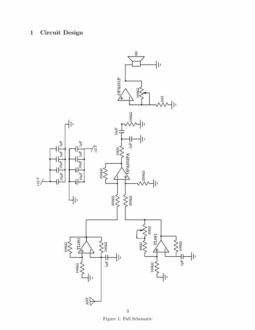
Figure 1: Full Schematic
3
While there are many theremin schematics available on the internet, they make compromises onvarious design aspects, i.e. cost, convenience, part availability, etc. I initially attempted to buildone of these pre-made designs, however I quickly gave up and began to design my own with bothsimplicity and ease of acquiring components in mind. Figure 1 on the preceding page depicts myfinal circuit.
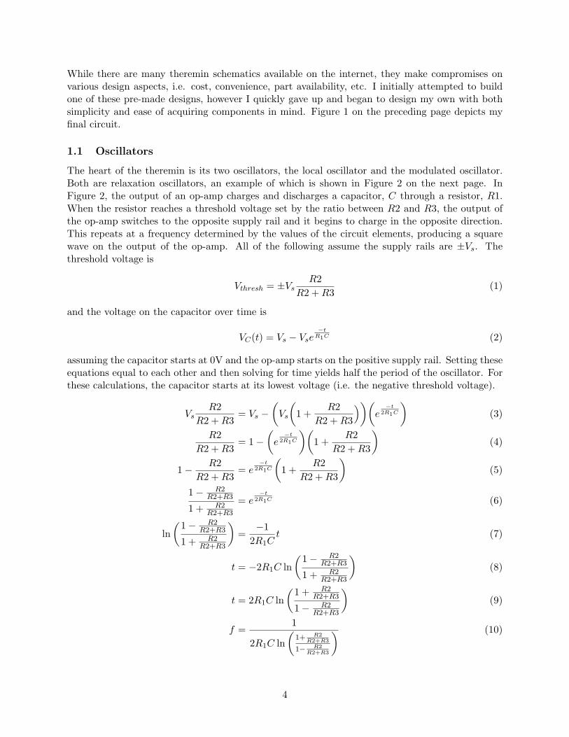
1.1 Oscillators
The heart of the theremin is its two oscillators, the local oscillator and the modulated oscillator.Both are relaxation oscillators, an example of which is shown in Figure 2 on the next page. InFigure 2, the output of an op-amp charges and discharges a capacitor, C through a resistor, R1.When the resistor reaches a threshold voltage set by the ratio between R2 and R3, the output ofthe op-amp switches to the opposite supply rail and it begins to charge in the opposite direction.This repeats at a frequency determined by the values of the circuit elements, producing a squarewave on the output of the op-amp. All of the following assume the supply rails are ±Vs. Thethreshold voltage is
Vthresh = ±VsR2
R2 +R3(1)
and the voltage on the capacitor over time is
VC(t) = Vs − Vse−t
R1C (2)
assuming the capacitor starts at 0V and the op-amp starts on the positive supply rail. Setting theseequations equal to each other and then solving for time yields half the period of the oscillator. Forthese calculations, the capacitor starts at its lowest voltage (i.e. the negative threshold voltage).
VsR2
R2 +R3= Vs −
(
Vs
(
1 +R2
R2 +R3
)
)(
e−t
2R1C
)
(3)
R2
R2 +R3= 1−
(
e−t
2R1C
)(
1 +R2
R2 +R3
)
(4)
1−R2
R2 +R3= e
−t
2R1C
(
1 +R2
R2 +R3
)
(5)
1− R2R2+R3
1 + R2R2+R3
= e−t
2R1C (6)
ln
(
1− R2R2+R3
1 + R2R2+R3
)
=−1
2R1Ct (7)
t = −2R1C ln
(
1− R2R2+R3
1 + R2R2+R3
)
(8)
t = 2R1C ln
(
1 + R2R2+R3
1− R2R2+R3
)
(9)
f =1
2R1C ln
(
1+ R2
R2+R3
1− R2
R2+R3
) (10)
4
and when R2 = R3
f =1
2R1C ln 3(11)
+
-
R2
C
R3
R1
VOUT
Figure 2: Relaxation Oscillator
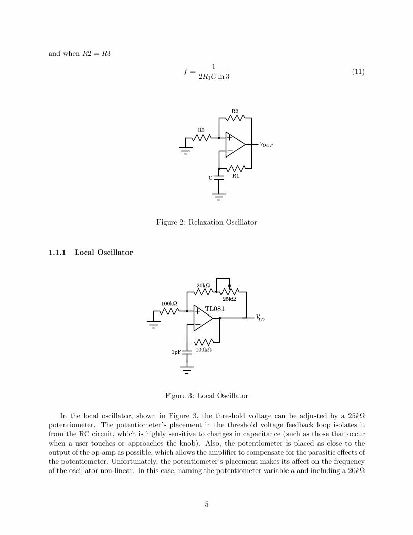
1.1.1 Local Oscillator
+
-
20kΩ
25kΩ100kΩ
100kΩ1pF
TL081VLO
Figure 3: Local Oscillator
In the local oscillator, shown in Figure 3, the threshold voltage can be adjusted by a 25kΩpotentiometer. The potentiometer’s placement in the threshold voltage feedback loop isolates itfrom the RC circuit, which is highly sensitive to changes in capacitance (such as those that occurwhen a user touches or approaches the knob). Also, the potentiometer is placed as close to theoutput of the op-amp as possible, which allows the amplifier to compensate for the parasitic effects ofthe potentiometer. Unfortunately, the potentiometer’s placement makes its affect on the frequencyof the oscillator non-linear. In this case, naming the potentiometer variable a and including a 20kΩ
5
resistor in series with the potentiometer, Equation (10) on page 4 yields the following:
f =1
2R1C ln
(
1+ R2
R2+R3
1− R2
R2+R3
) (12)
R1 = 100kΩ (13)
R2 = 20kΩ+ a(25kΩ) (14)
R3 = 100kΩ (15)
C = 1pF (16)
flo =1
(100kΩ)(1pF ) ln
(1 + 20kΩ+a(25kΩ)120kΩ+a(25kΩ)
1− 20kΩ+a(25kΩ)120kΩ+a(25kΩ)
)
(17)
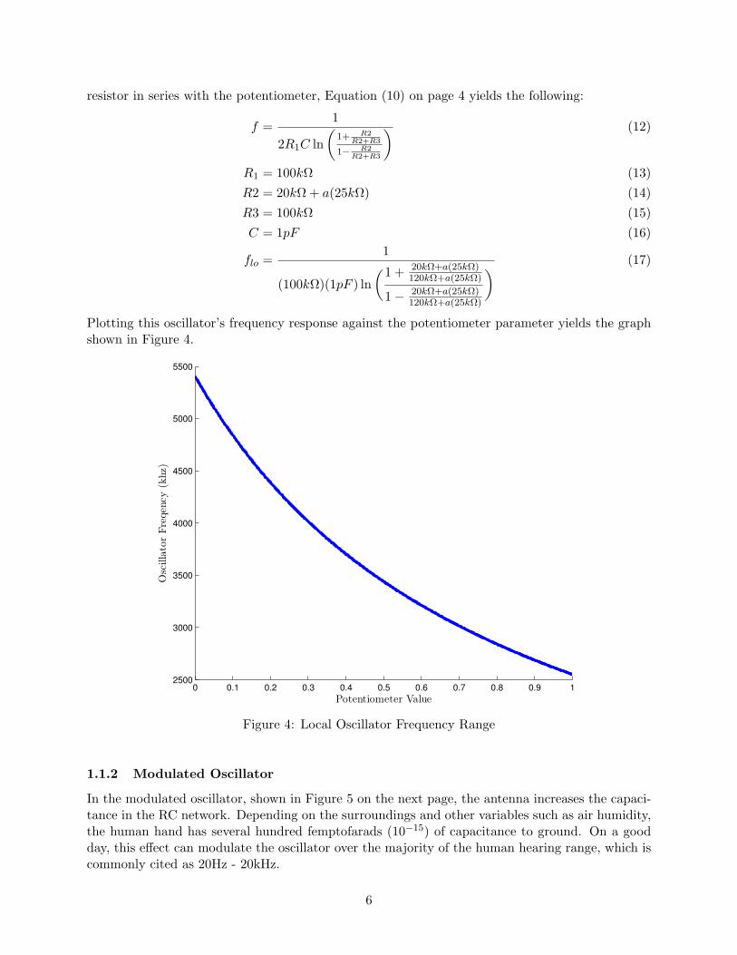
Plotting this oscillator’s frequency response against the potentiometer parameter yields the graphshown in Figure 4.
0 0.1 0.2 0.3 0.4 0.5 0.6 0.7 0.8 0.9 12500
3000
3500
4000
4500
5000
5500
Potentiometer Value
OscillatorFreqency
(khz)
Figure 4: Local Oscillator Frequency Range
1.1.2 Modulated Oscillator
In the modulated oscillator, shown in Figure 5 on the next page, the antenna increases the capaci-tance in the RC network. Depending on the surroundings and other variables such as air humidity,the human hand has several hundred femptofarads (10−15) of capacitance to ground. On a goodday, this effect can modulate the oscillator over the majority of the human hearing range, which iscommonly cited as 20Hz - 20kHz.
6
+
-
100kΩ
1pF
TL081100kΩ
ANT
100kΩ
VMO
Figure 5: Modulated Oscillator
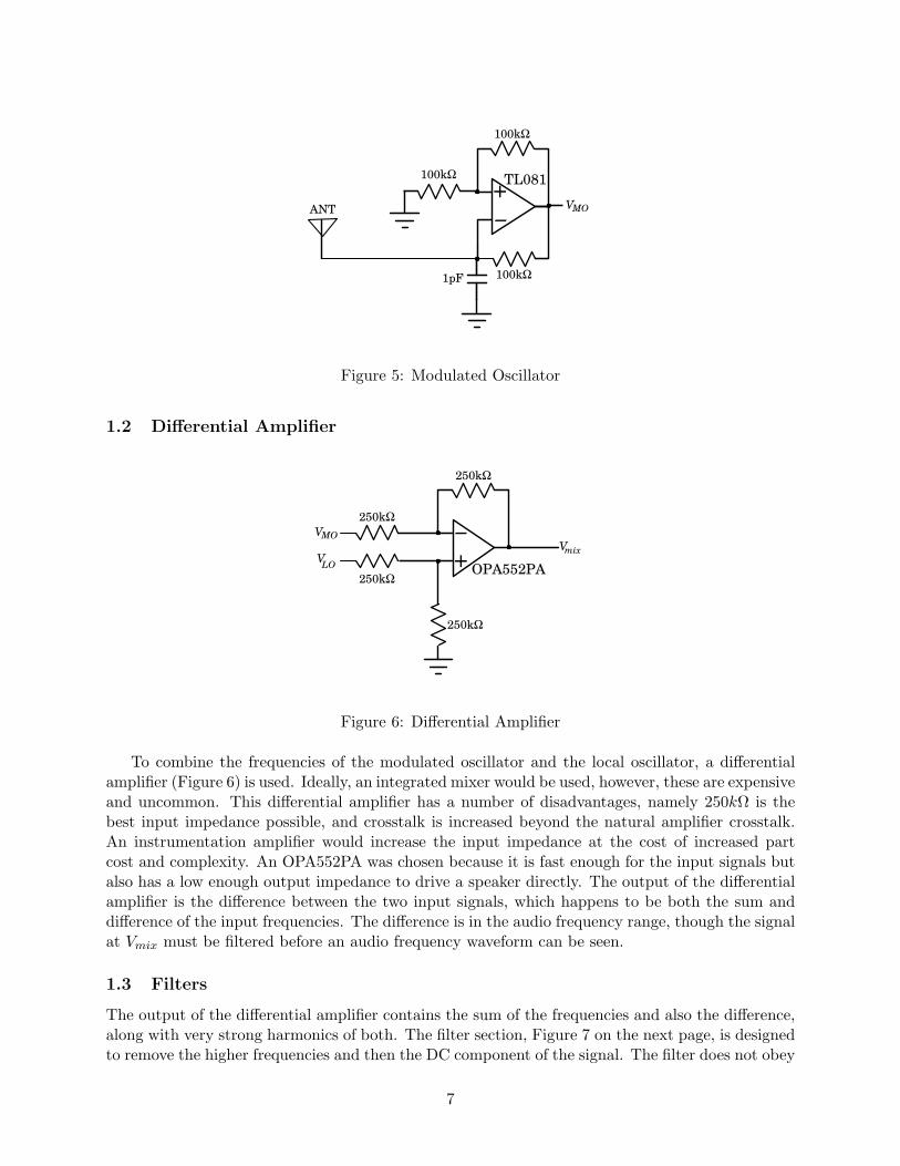
1.2 Differential Amplifier
+
-250kΩ
250kΩ
250kΩ
250kΩOPA552PA
Vmix
VMO
VLO
Figure 6: Differential Amplifier
To combine the frequencies of the modulated oscillator and the local oscillator, a differentialamplifier (Figure 6) is used. Ideally, an integrated mixer would be used, however, these are expensiveand uncommon. This differential amplifier has a number of disadvantages, namely 250kΩ is thebest input impedance possible, and crosstalk is increased beyond the natural amplifier crosstalk.An instrumentation amplifier would increase the input impedance at the cost of increased partcost and complexity. An OPA552PA was chosen because it is fast enough for the input signals butalso has a low enough output impedance to drive a speaker directly. The output of the differentialamplifier is the difference between the two input signals, which happens to be both the sum anddifference of the input frequencies. The difference is in the audio frequency range, though the signalat Vmix must be filtered before an audio frequency waveform can be seen.
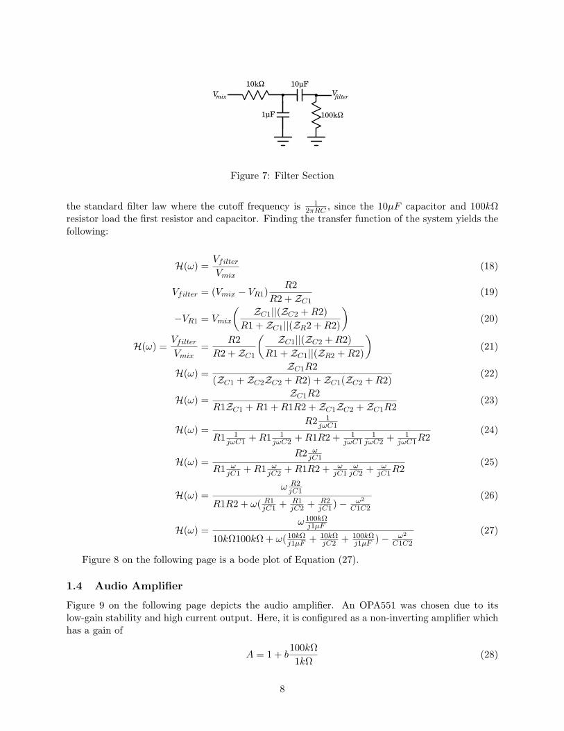
1.3 Filters
The output of the differential amplifier contains the sum of the frequencies and also the difference,along with very strong harmonics of both. The filter section, Figure 7 on the next page, is designedto remove the higher frequencies and then the DC component of the signal. The filter does not obey
7
10kΩ
1µF
10µF
100kΩ
VfilterVmix
Figure 7: Filter Section
the standard filter law where the cutoff frequency is 12πRC
, since the 10µF capacitor and 100kΩresistor load the first resistor and capacitor. Finding the transfer function of the system yields thefollowing:
H(ω) =Vfilter
Vmix(18)
Vfilter = (Vmix − VR1)R2
R2 + ZC1(19)
−VR1 = Vmix
(
ZC1||(ZC2 +R2)
R1 + ZC1||(ZR2 +R2)
)
(20)
H(ω) =Vfilter
Vmix=
R2
R2 + ZC1
(
ZC1||(ZC2 +R2)
R1 + ZC1||(ZR2 +R2)
)
(21)
H(ω) =ZC1R2
(ZC1 + ZC2ZC2 +R2) + ZC1(ZC2 +R2)(22)
H(ω) =ZC1R2
R1ZC1 +R1 +R1R2 + ZC1ZC2 + ZC1R2(23)
H(ω) =R2 1
jωC1
R1 1jωC1 +R1 1
jωC2 +R1R2 + 1jωC1
1jωC2 + 1
jωC1R2(24)
H(ω) =R2 ω
jC1
R1 ωjC1 +R1 ω
jC2 +R1R2 + ωjC1
ωjC2 + ω
jC1R2(25)
H(ω) =ω R2
jC1
R1R2 + ω( R1jC1 + R1
jC2 + R2jC1)−
ω2
C1C2
(26)
H(ω) =ω 100kΩ
j1µF
10kΩ100kΩ+ ω( 10kΩj1µF + 10kΩ
jC2 + 100kΩj1µF )− ω2
C1C2
(27)
Figure 8 on the following page is a bode plot of Equation (27).
1.4 Audio Amplifier
Figure 9 on the following page depicts the audio amplifier. An OPA551 was chosen due to itslow-gain stability and high current output. Here, it is configured as a non-inverting amplifier whichhas a gain of
A = 1 + b100kΩ
1kΩ(28)
8

10−2
10−1
100
101
102
103
104
105
−90
−80
−70
−60
−50
−40
−30
−20
−10
0
Magnitude(dB)
Frequency (Hz)
Figure 8: Filter Bode Plot
depending, of course, on the potentiometer variable b. Since the mixer outputs the signal clippedby the rails, the amplifier is primarily to counter the attenuation of the filter. Additionally, sincethe filter reduces the harmonics in the signal significantly, the high possible gain of the amplifiercan be used like a tone control to add the harmonics back in by clipping the signal.
+
-
1kΩ
100kΩ8Ω
OPA551PVfilter
Figure 9: Audio Amplifier
9
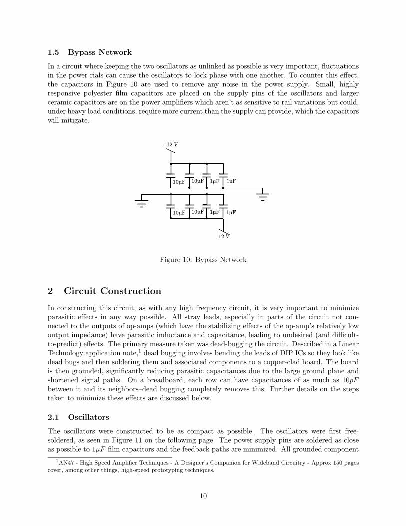
1.5 Bypass Network
In a circuit where keeping the two oscillators as unlinked as possible is very important, fluctuationsin the power rials can cause the oscillators to lock phase with one another. To counter this effect,the capacitors in Figure 10 are used to remove any noise in the power supply. Small, highlyresponsive polyester film capacitors are placed on the supply pins of the oscillators and largerceramic capacitors are on the power amplifiers which aren’t as sensitive to rail variations but could,under heavy load conditions, require more current than the supply can provide, which the capacitorswill mitigate.
10µF 10µF 1µF 1µF
10µF 10µF 1µF 1µF
+12 V
-12 V
Figure 10: Bypass Network
2 Circuit Construction
In constructing this circuit, as with any high frequency circuit, it is very important to minimizeparasitic effects in any way possible. All stray leads, especially in parts of the circuit not con-nected to the outputs of op-amps (which have the stabilizing effects of the op-amp’s relatively lowoutput impedance) have parasitic inductance and capacitance, leading to undesired (and difficult-to-predict) effects. The primary measure taken was dead-bugging the circuit. Described in a LinearTechnology application note,1 dead bugging involves bending the leads of DIP ICs so they look likedead bugs and then soldering them and associated components to a copper-clad board. The boardis then grounded, significantly reducing parasitic capacitances due to the large ground plane andshortened signal paths. On a breadboard, each row can have capacitances of as much as 10pFbetween it and its neighbors–dead bugging completely removes this. Further details on the stepstaken to minimize these effects are discussed below.
2.1 Oscillators
The oscillators were constructed to be as compact as possible. The oscillators were first free-soldered, as seen in Figure 11 on the following page. The power supply pins are soldered as closeas possible to 1µF film capacitors and the feedback paths are minimized. All grounded component
1AN47 - High Speed Amplifier Techniques - A Designer’s Companion for Wideband Circuitry - Approx 150 pages
cover, among other things, high-speed prototyping techniques.
10
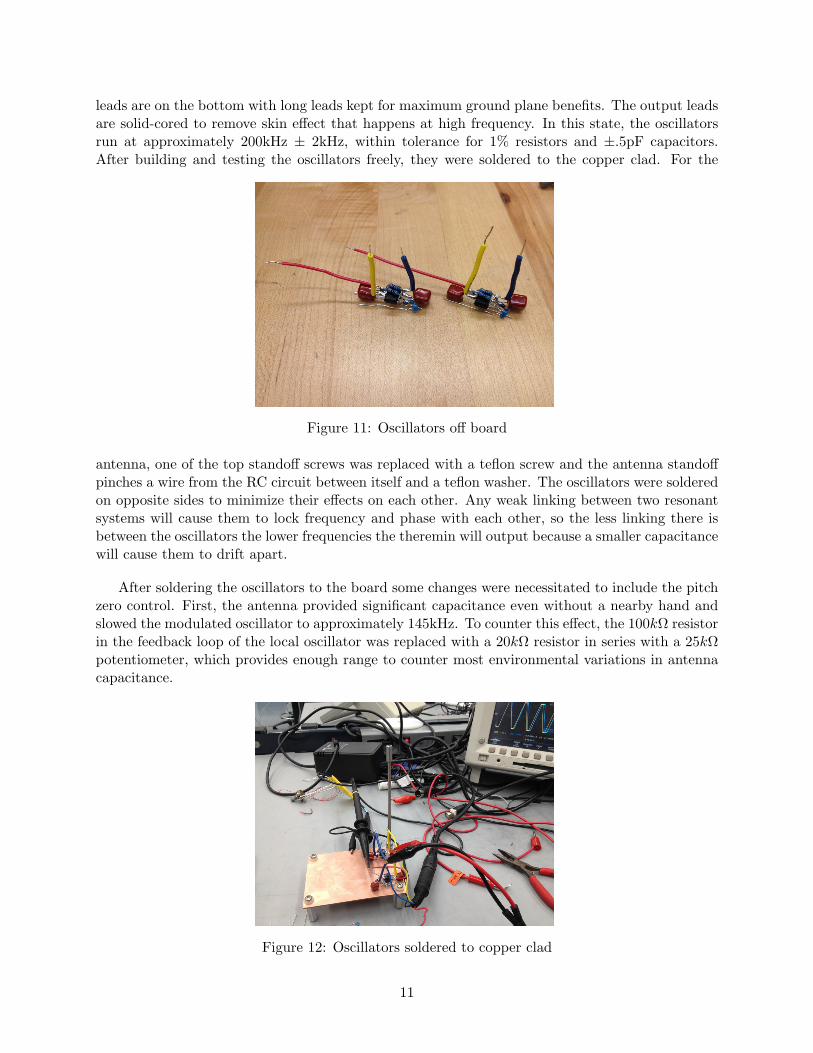
leads are on the bottom with long leads kept for maximum ground plane benefits. The output leadsare solid-cored to remove skin effect that happens at high frequency. In this state, the oscillatorsrun at approximately 200kHz ± 2kHz, within tolerance for 1% resistors and ±.5pF capacitors.After building and testing the oscillators freely, they were soldered to the copper clad. For the
Figure 11: Oscillators off board
antenna, one of the top standoff screws was replaced with a teflon screw and the antenna standoffpinches a wire from the RC circuit between itself and a teflon washer. The oscillators were solderedon opposite sides to minimize their effects on each other. Any weak linking between two resonantsystems will cause them to lock frequency and phase with each other, so the less linking there isbetween the oscillators the lower frequencies the theremin will output because a smaller capacitancewill cause them to drift apart.
After soldering the oscillators to the board some changes were necessitated to include the pitchzero control. First, the antenna provided significant capacitance even without a nearby hand andslowed the modulated oscillator to approximately 145kHz. To counter this effect, the 100kΩ resistorin the feedback loop of the local oscillator was replaced with a 20kΩ resistor in series with a 25kΩpotentiometer, which provides enough range to counter most environmental variations in antennacapacitance.
Figure 12: Oscillators soldered to copper clad
11
2.2 Differential Amplifier
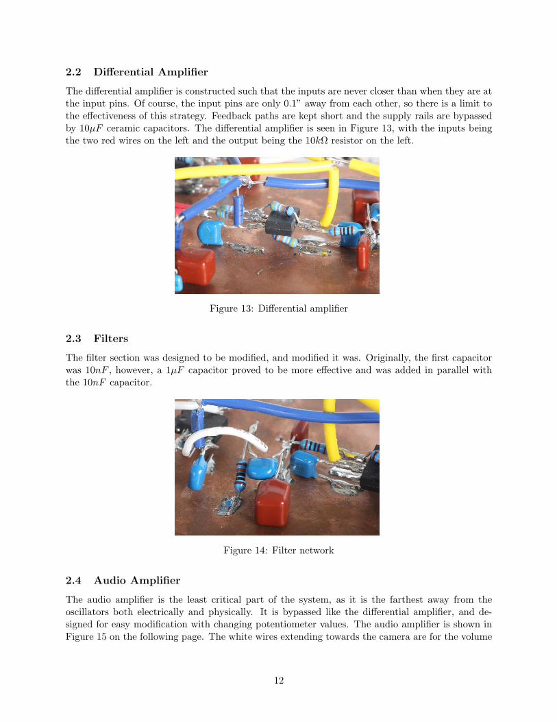
The differential amplifier is constructed such that the inputs are never closer than when they are atthe input pins. Of course, the input pins are only 0.1” away from each other, so there is a limit tothe effectiveness of this strategy. Feedback paths are kept short and the supply rails are bypassedby 10µF ceramic capacitors. The differential amplifier is seen in Figure 13, with the inputs beingthe two red wires on the left and the output being the 10kΩ resistor on the left.
Figure 13: Differential amplifier
2.3 Filters
The filter section was designed to be modified, and modified it was. Originally, the first capacitorwas 10nF , however, a 1µF capacitor proved to be more effective and was added in parallel withthe 10nF capacitor.
Figure 14: Filter network
2.4 Audio Amplifier
The audio amplifier is the least critical part of the system, as it is the farthest away from theoscillators both electrically and physically. It is bypassed like the differential amplifier, and de-signed for easy modification with changing potentiometer values. The audio amplifier is shown inFigure 15 on the following page. The white wires extending towards the camera are for the volume
12

potentiometer, the purple wire is an (unused) thermal overload detection, and the red wire is theoutput.
Figure 15: Audio amplifier
3 Case Design and Construction
The case is designed to be constructed from ” MDF, mostly because enough scrap ” MDF wasavailable for a 4”×3”×7” box. All the box panels were cut on a laser cutter in the Olin machineshop. To laser cut the box, it was first necessary to made CAD files of the theremin. Figure 16ais an exploded rendering, and Figure 16b is the theremin assembled. For comparison, the fullyassembled theremin is seen in Figure 17 on the next page.
(a) Exploded render (b) Assembled Render
Figure 16: Renders
3.1 Front Panel
The front panel is designed for the two panel mount potentiometers that were available. Unfortu-nately, potentiometers with a ”-20 bushing are very hard to find with bushings longer than ”. Tosolve this problem, an end mill was used to counterbore the reverse of the front panel. The text onthe faceplate is engraved with the laser cutter.
13

Figure 17: Fully assmbled
3.2 Power Input
Due to the unavailability of a true panel-mount power input, an inline-wired female DIN-5 connectorwas re-purposed as a panel mount jack with the help of some hot glue, as seen in Figure 18.
(a) Inside of power jack (b) Outside of power jack
Figure 18: DIN-5 Connector
3.3 Speaker Output
The speaker outputs are on the opposite side of the theremin from the power input, and are a pairof banana jacks, spaced the standard .75” apart for compatibility with dual banana plugs, as seenin Figure 19 on the next page.
14
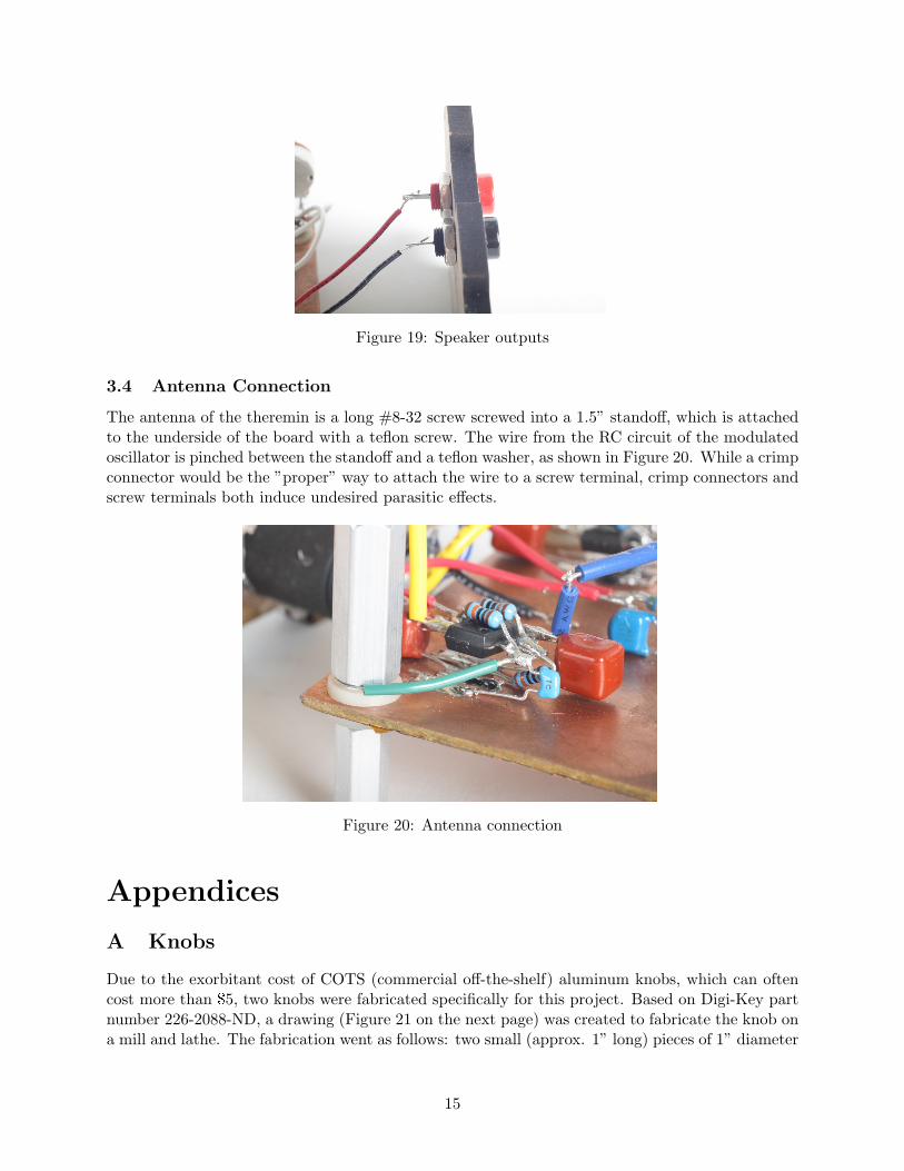
Figure 19: Speaker outputs
3.4 Antenna Connection
The antenna of the theremin is a long #8-32 screw screwed into a 1.5” standoff, which is attachedto the underside of the board with a teflon screw. The wire from the RC circuit of the modulatedoscillator is pinched between the standoff and a teflon washer, as shown in Figure 20. While a crimpconnector would be the ”proper” way to attach the wire to a screw terminal, crimp connectors andscrew terminals both induce undesired parasitic effects.
Figure 20: Antenna connection
Appendices
A Knobs
Due to the exorbitant cost of COTS (commercial off-the-shelf) aluminum knobs, which can oftencost more than 5, two knobs were fabricated specifically for this project. Based on Digi-Key partnumber 226-2088-ND, a drawing (Figure 21 on the next page) was created to fabricate the knob ona mill and lathe. The fabrication went as follows: two small (approx. 1” long) pieces of 1” diameter
15

PITC
H .2
5 RA
ISED
DIA
MO
ND
KN
URL
.062
5 135
°
.150
.4
45
.500
.375
.250
.010
0
.120 .157
.510
.625
.338
#6-
32 S
ET S
CRE
W
AD
O N
OT
SCA
LE D
RAW
ING
Knob
SHEE
T 1 O
F 1
12/7
/12
12/7
/12
FES
FAB
UNLE
SS O
THER
WIS
E SP
ECIF
IED
:
SCA
LE: 1
:1W
EIG
HT: 3
.6g
REV
DW
G.
ASIZE
TITLE
: Kno
b fo
r Fal
l 201
2 M
odC
on F
inal
Proj
ect
NA
ME
DA
TE
CO
MM
ENTS
: Bas
ed o
n D
igi-K
ey P
/N 2
26-2
088-
ND
and
ass
ocia
ted
draw
ings
from
Kilo
Inte
rnat
iona
l.
MFG
APP
R.
ENG
APP
R.
CHE
CKE
D
DRA
WN
6061
Alu
m. .
75" S
tock
FIN
ISH:
125
MA
TERI
AL
ALL
SM
ALL
FILL
ETS
.020
-.040
DIM
ENSI
ON
S A
RE IN
INC
HES
TOLE
RAN
CES
:.X
=.0
3.X
X =
.01
.XXX
=
.005
PRO
PRIE
TARY
AN
D C
ON
FIDE
NTIA
LTH
E IN
FORM
ATIO
N C
ON
TAIN
ED IN
THI
SD
RAW
ING
IS T
HE S
OLE
PRO
PERT
Y O
FFO
RRES
T BO
URKE
. A
NY
REPR
OD
UCTIO
N
IN P
ART
OR
AS
A W
HOLE
WITH
OUT
THE
W
RITT
EN P
ERM
ISSI
ON
OF
FORR
EST
BOUR
KE IS
PRO
HIBI
TED
. REA
LLY
THO
UGH,
I DO
N'T
CA
RE W
HAT
YOU
DO
WITH
IT.
53
21
Forre
st B
ourk
e
Figure 21: Knob Drawing
16
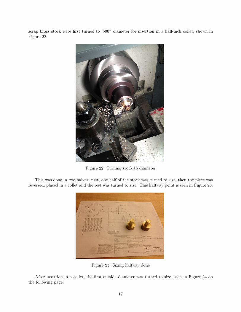
scrap brass stock were first turned to .500” diameter for insertion in a half-inch collet, shown inFigure 22.
Figure 22: Turning stock to diameter
This was done in two halves: first, one half of the stock was turned to size, then the piece wasreversed, placed in a collet and the rest was turned to size. This halfway point is seen in Figure 23.
Figure 23: Sizing halfway done
After insertion in a collet, the first outside diameter was turned to size, seen in Figure 24 onthe following page.
17
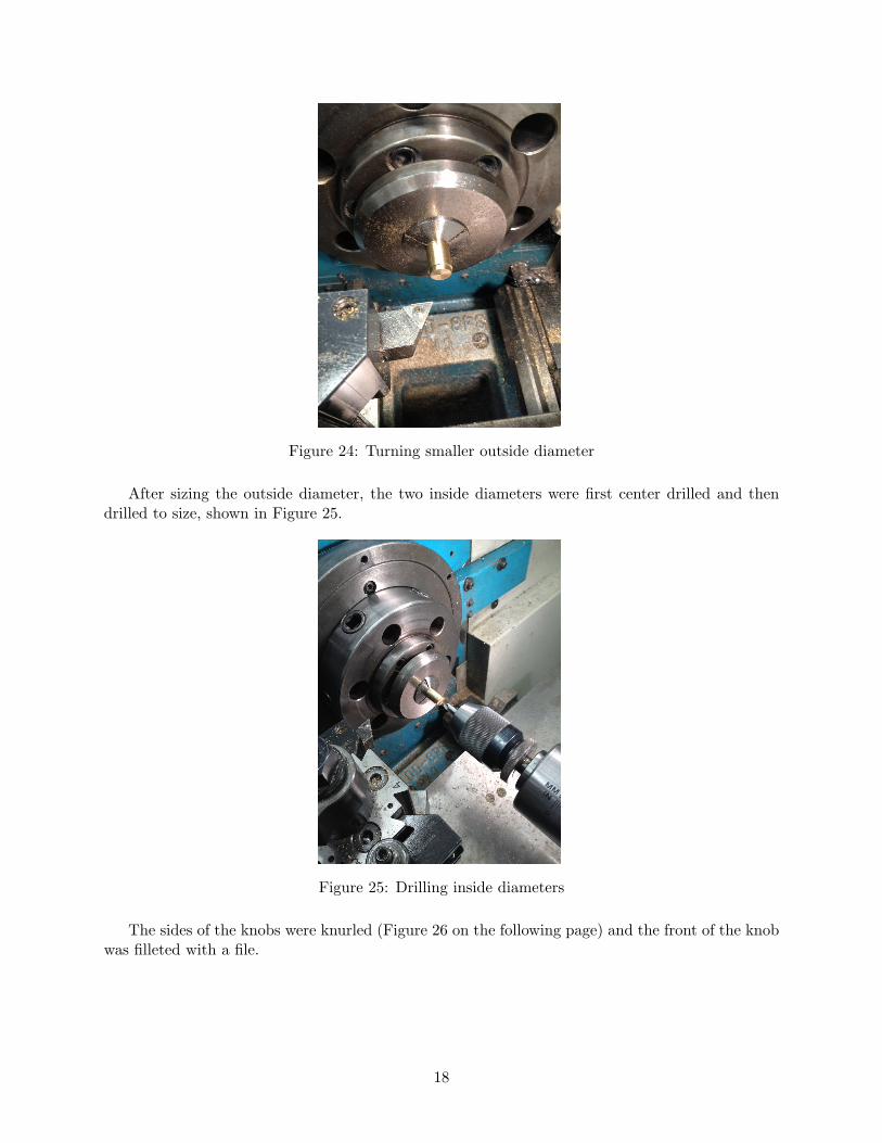
Figure 24: Turning smaller outside diameter
After sizing the outside diameter, the two inside diameters were first center drilled and thendrilled to size, shown in Figure 25.
Figure 25: Drilling inside diameters
The sides of the knobs were knurled (Figure 26 on the following page) and the front of the knobwas filleted with a file.
18
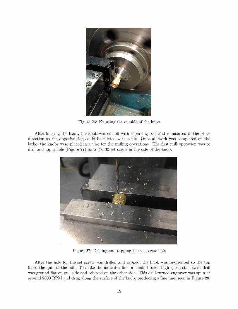
Figure 26: Knurling the outside of the knob
After filleting the front, the knob was cut off with a parting tool and re-inserted in the otherdirection so the opposite side could be filleted with a file. Once all work was completed on thelathe, the knobs were placed in a vise for the milling operations. The first mill operation was todrill and tap a hole (Figure 27) for a #6-32 set screw in the side of the knob.
Figure 27: Drilling and tapping the set screw hole
After the hole for the set screw was drilled and tapped, the knob was re-oriented so the topfaced the quill of the mill. To make the indicator line, a small, broken high-speed steel twist drillwas ground flat on one side and relieved on the other side. This drill-turned-engraver was spun ataround 2000 RPM and drug along the surface of the knob, producing a fine line, seen in Figure 28.
19
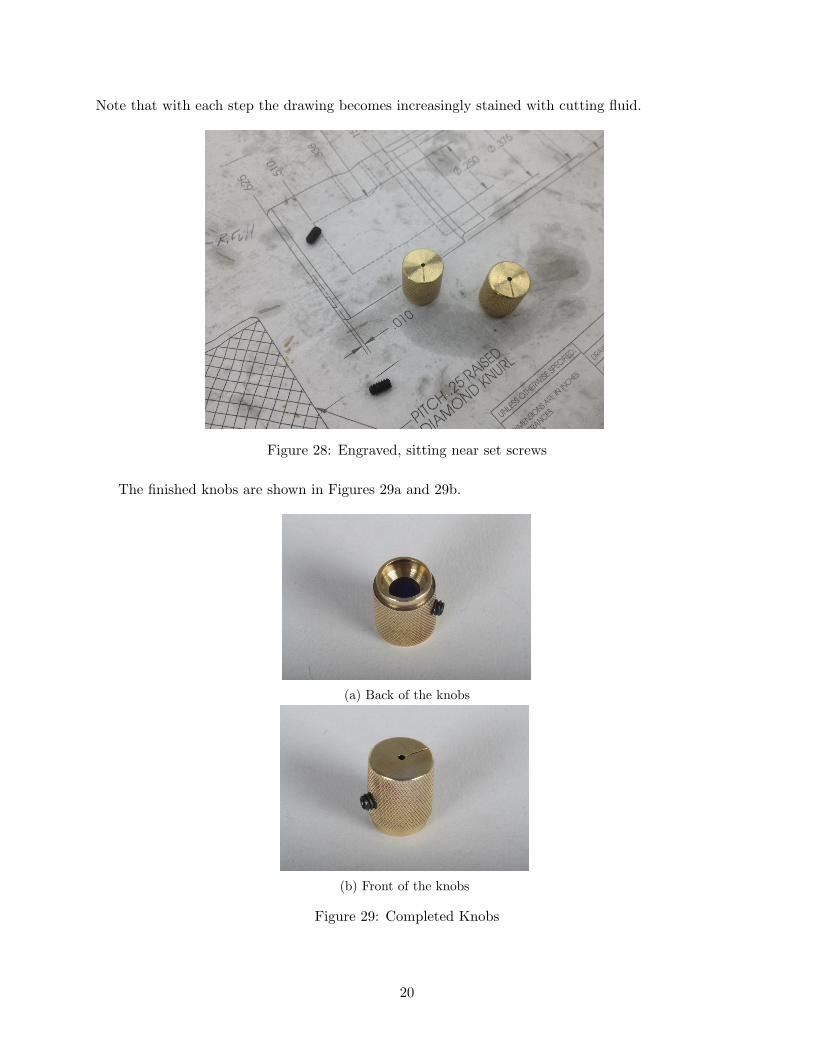
Note that with each step the drawing becomes increasingly stained with cutting fluid.
Figure 28: Engraved, sitting near set screws
The finished knobs are shown in Figures 29a and 29b.
(a) Back of the knobs
(b) Front of the knobs
Figure 29: Completed Knobs
20