mips32 4k™ processor core family software user’s … 4k processor core family software user’s...
TRANSCRIPT

Document Number: MD00016Revision 01.17
September 25, 2002
MIPS Technologies, Inc.1225 Charleston Road
Mountain View, CA 94043-1353
Copyright © 1998-2002 MIPS Technologies Inc. All rights reserved.
MIPS32 4K™Processor Core Family
Software User’s Manual
Copyright © 1998-2002 MIPS Technologies, Inc. All rights reserved.
Unpublished rights (if any) are reserved under the Copyright Laws of the United States of America.
If this document is provided in source format (i.e., in a modifiable form such as in FrameMaker or Microsoft Word format), thenits use and distribution is subject to a written agreement with MIPS Technologies, Inc. ("MIPS Technologies"). UNDER NOCIRCUMSTANCES MAY A DOCUMENT PROVIDED IN SOURCE FORMAT BE DISTRIBUTED TO A THIRD PARTYWITHOUT THE EXPRESS WRITTEN CONSENT OF MIPS TECHNOLOGIES.
This document contains information that is proprietary to MIPS Technologies. Any copying, reproducing, modifying, or use ofthis information (in whole or in part) which is not expressly permitted in writing by MIPS Technologies or acontractually-authorized third party is strictly prohibited. At a minimum, this information is protected under unfair competitionand copyright laws. Violations thereof may result in criminal penalties and fines.
MIPS Technologies or any contractually-authorized third party reserves the right to change the information contained in thisdocument to improve function, design or otherwise. MIPS Technologies does not assume any liability arising out of theapplication or use of this information, or of any error of omission in such information. Any warranties, whether express,statutory, implied or otherwise, including but not limited to the implied warranties of merchantability or fitness for a particularpurpose, are excluded. Any license under patent rights or any other intellectual property rights owned by MIPS Technologiesor third parties shall be conveyed by MIPS Technologies or any contractually-authorized third party in a separate licenseagreement between the parties.
The information contained in this document shall not be exported or transferred for the purpose of reexporting in violation ofany U.S. or non-U.S. regulation, treaty, Executive Order, law, statute, amendment or supplement thereto.
The information contained in this document constitutes one or more of the following: commercial computer software,commercial computer software documentation or other commercial items. If the user of this information, or any relateddocumentation of any kind, including related technical data or manuals, is an agency, department, or other entity of the UnitedStates government (“Government”), the use, duplication, reproduction, release, modification, disclosure, or transfer of thisinformation, or any related documentation of any kind, is restricted in accordance with Federal Acquisition Regulation 12.212for civilian agencies and Defense Federal Acquisition Regulation Supplement 227.7202 for military agencies. The use of thisinformation by the Government is further restricted in accordance with the terms of the license agreement(s) and/or applicablecontract terms and conditions covering this information from MIPS Technologies or any contractually-authorized third party.
MIPS®, R3000®, R4000®, R5000® and R10000® are among the registered trademarks of MIPS Technologies, Inc. in theUnited States and certain other countries, and MIPS16™, MIPS16e™, MIPS32™, MIPS64™, MIPS-3D™, MIPS-based™,MIPS I™, MIPS II™, MIPS III™, MIPS IV™, MIPS V™, MDMX™, MIPSsim™, MIPSsimCA™, MIPSsimIA™,QuickMIPS™, SmartMIPS™, MIPS Technologies logo, 4K™, 4Kc™, 4Km™, 4Kp™, 4KE™, 4KEc™, 4KEm™, 4KEp™,4KS™, 4KSc™, M4K™, 5K™, 5Kc™, 5Kf™, 20K™, 20Kc™, 25Kf™, R4300™, ASMACRO™, ATLAS™, BusBridge™,CoreFPGA™, CoreLV™, EC™, JALGO™, MALTA™, MGB™, PDtrace™, SEAD™, SEAD-2™, SOC-it™, The Pipeline™,and YAMON™ are among the trademarks of MIPS Technologies, Inc.
All other trademarks referred to herein are the property of their respective owners.
Template: B1.06, Build with Conditional Tags: 2B JADE MIPS32 PROCMIPS32 4K™ Processor Core Family Software User’s Manual, Revision 01.17
Copyright © 1998-2002 MIPS Technologies Inc. All rights reserved.

MIPS32 4K™ Processor Core Family Software User’s Manual, Revision 01.17 iii
Copyright © 1998-2002 MIPS Technologies Inc. All rights reserved.
References to Product Names
This manual encompasses the 4Kc™, 4Km™ & 4Kp™ processor cores. The three products are similar in design, hencethe majority of information contained in this manual refers to all three cores.
Throughout this manual the terms “the core” or “the processor” refers to the 4Kc™, 4Km™, and 4Kp™ devices. Someinformation in this manual, specifically in Chapters 2 and 4, is specific to one or more of the cores, but not all three. Thisinformation is called out in the text wherever necessary. For example, the section dealing with the TLB is denoted asbeing 4Kc™ core specific, whereas the section dealing with the BAT is denoted as being 4Km™ and 4Kp™ corespecific.
Product Differentiation
The three products contained in this manual are similar in design. The main differences are in memory management andthe multiply-divide unit. In general the differences are as follows:
4Kc™ processor: Contains pipelined multiplier and translation lookaside buffer (TLB).
4Km™ processor: Contains pipelined multiplier and block address translator (BAT).
4Kp™ processor: Contains non-pipelined multiplier and block address translator (BAT).

Table of Contents
Chapter 1 Introduction to the MIPS32 4K™ Processor Core Family ...................................................................................11.1 Features ...................................................................................................................................................................21.2 Block Diagram ........................................................................................................................................................31.3 Required Logic Blocks ............................................................................................................................................4
1.3.1 Execution Unit ..............................................................................................................................................41.3.2 Multiply/Divide Unit (MDU) .......................................................................................................................51.3.3 System Control Coprocessor (CP0) ..............................................................................................................51.3.4 Memory Management Unit (MMU) .............................................................................................................51.3.5 Cache Controllers ..........................................................................................................................................71.3.6 Bus Interface Unit (BIU) ..............................................................................................................................71.3.7 Power Management ......................................................................................................................................7
1.4 Optional Logic Blocks ............................................................................................................................................81.4.1 Instruction Cache ..........................................................................................................................................81.4.2 Data Cache ....................................................................................................................................................81.4.3 EJTAG Controller .........................................................................................................................................8
Chapter 2 Pipeline ...............................................................................................................................................................112.1 Pipeline Stages ......................................................................................................................................................11
2.1.1 I Stage: Instruction Fetch ............................................................................................................................132.1.2 E Stage: Execution ......................................................................................................................................132.1.3 M Stage: Memory Fetch .............................................................................................................................132.1.4 A Stage: Align/Accumulate ........................................................................................................................132.1.5 W Stage: Writeback ....................................................................................................................................14
2.2 Instruction Cache Miss ..........................................................................................................................................142.3 Data Cache Miss ...................................................................................................................................................152.4 Multiply/Divide Operations ..................................................................................................................................162.5 MDU Pipeline (4Kc and 4Km Cores) ...................................................................................................................16
2.5.1 32x16 Multiply (4Kc and 4Km Cores) .......................................................................................................192.5.2 32x32 Multiply (4Kc and 4Km Cores) .......................................................................................................192.5.3 Divide (4Kc and 4Km Cores) .....................................................................................................................19
2.6 MDU Pipeline (4Kp Core Only) ...........................................................................................................................212.6.1 Multiply (4Kp Core) ...................................................................................................................................212.6.2 Multiply Accumulate (4Kp Core) ...............................................................................................................222.6.3 Divide (4Kp Core) ......................................................................................................................................22
2.7 Branch Delay .........................................................................................................................................................232.8 Data Bypassing .....................................................................................................................................................23
2.8.1 Load Delay ..................................................................................................................................................242.8.2 Move from HI/LO and CP0 Delay ..............................................................................................................25
2.9 Interlock Handling ................................................................................................................................................252.10 Slip Conditions ....................................................................................................................................................262.11 Instruction Interlocks ..........................................................................................................................................272.12 Instruction Hazards .............................................................................................................................................28
Chapter 3 Memory Management .........................................................................................................................................313.1 Introduction ...........................................................................................................................................................313.2 Modes of Operation ..............................................................................................................................................32
3.2.1 Virtual Memory Segments ..........................................................................................................................333.2.2 User Mode ...................................................................................................................................................353.2.3 Kernel Mode ...............................................................................................................................................363.2.4 Debug Mode ................................................................................................................................................38
3.3 Translation Lookaside Buffer (4Kc Core Only) ...................................................................................................40
iv MIPS32 4K™ Processor Core Family Software User’s Manual, Revision 01.17
Copyright © 1998-2002 MIPS Technologies Inc. All right reserved.
6263
78
.
.
.86
3.3.1 Joint TLB ....................................................................................................................................................403.3.2 Instruction TLB ...........................................................................................................................................423.3.3 Data TLB ....................................................................................................................................................43
3.4 Virtual to Physical Address Translation (4Kc Core) ............................................................................................433.4.1 Hits, Misses, and Multiple Matches ............................................................................................................453.4.2 Page Sizes and Replacement Algorithm .....................................................................................................463.4.3 TLB Instructions .........................................................................................................................................47
3.5 Fixed Mapping MMU (4Km & 4Kp Cores) .........................................................................................................473.6 System Control Coprocessor .................................................................................................................................49
Chapter 4 Exceptions ..........................................................................................................................................................514.1 Exception Conditions ............................................................................................................................................514.2 Exception Priority .................................................................................................................................................524.3 Exception Vector Locations ..................................................................................................................................534.4 General Exception Processing ..............................................................................................................................544.5 Debug Exception Processing ................................................................................................................................554.6 Exceptions .............................................................................................................................................................56
4.6.1 Reset Exception ..........................................................................................................................................564.6.2 Soft Reset Exception ...................................................................................................................................574.6.3 Debug Single Step Exception .....................................................................................................................584.6.4 Debug Interrupt Exception ..........................................................................................................................594.6.5 Non-Maskable Interrupt (NMI) Exception .................................................................................................594.6.6 Machine Check Exception (4Kc core) ........................................................................................................604.6.7 Interrupt Exception .....................................................................................................................................604.6.8 Debug Instruction Break Exception ............................................................................................................604.6.9 Watch Exception — Instruction Fetch or Data Access ..............................................................................614.6.10 Address Error Exception — Instruction Fetch/Data Access .....................................................................614.6.11 TLB Refill Exception — Instruction Fetch or Data Access (4Kc core) ...................................................4.6.12 TLB Invalid Exception — Instruction Fetch or Data Access (4Kc core) .................................................4.6.13 Bus Error Exception — Instruction Fetch or Data Access .......................................................................634.6.14 Debug Software Breakpoint Exception ....................................................................................................644.6.15 Execution Exception — System Call ........................................................................................................644.6.16 Execution Exception — Breakpoint .........................................................................................................644.6.17 Execution Exception — Reserved Instruction ..........................................................................................644.6.18 Execution Exception — Coprocessor Unusable .......................................................................................654.6.19 Execution Exception — Integer Overflow ...............................................................................................654.6.20 Execution Exception — Trap ....................................................................................................................654.6.21 Debug Data Break Exception ....................................................................................................................664.6.22 TLB Modified Exception — Data Access (4Kc core) ..............................................................................66
4.7 Exception Handling and Servicing Flowcharts .....................................................................................................67
Chapter 5 CP0 Registers .....................................................................................................................................................735.1 CP0 Register Summary .........................................................................................................................................735.2 CP0 Registers ........................................................................................................................................................75
5.2.1Index Register (CP0 Register 0, Select 0) ...................................................................................................765.2.2Random Register (CP0 Register 1, Select 0) ..............................................................................................775.2.3EntryLo0, EntryLo1 (CP0 Registers 2 and 3, Select 0) ..............................................................................5.2.4Context Register (CP0 Register 4, Select 0) ...............................................................................................805.2.5PageMask Register (CP0 Register 5, Select 0) ..........................................................................................815.2.6Wired Register (CP0 Register 6, Select 0) ..................................................................................................825.2.7BadVAddr Register (CP0 Register 8, Select 0) ..........................................................................................835.2.8Count Register (CP0 Register 9, Select 0) ..................................................................................................845.2.9EntryHi Register (CP0 Register 10, Select 0) .............................................................................................855.2.10 Compare Register (CP0 Register 11, Select 0) .......................................................................................5.2.11Status Register (CP0 Register 12, Select 0) ..............................................................................................875.2.12Cause Register (CP0 Register 13, Select 0) ..............................................................................................91
MIPS32 4K™ Processor Core Family Software User’s Manual, Revision 01.17 v
Copyright © 1998-2002 MIPS Technologies Inc. All right reserved.

.10
5.2.13 Exception Program Counter (CP0 Register 14, Select 0) .........................................................................935.2.14 Processor Identification (CP0 Register 15, Select 0) ................................................................................945.2.15Config Register (CP0 Register 16, Select 0) .............................................................................................955.2.16Config1 Register (CP0 Register 16, Select 1) ...........................................................................................985.2.17 Load Linked Address (CP0 Register 17, Select 0) ...................................................................................995.2.18WatchLo Register (CP0 Register 18) ......................................................................................................1005.2.19WatchHi Register (CP0 Register 19) ......................................................................................................1015.2.20Debug Register (CP0 Register 23) ..........................................................................................................1025.2.21 Debug Exception Program Counter Register (CP0 Register 24) ...........................................................55.2.22ErrCtl Register (CP0 Register 26, Select 0) ...........................................................................................1065.2.23TagLo Register (CP0 Register 28, Select 0) ...........................................................................................1065.2.24DataLo Register (CP0 Register 28, Select 1) .........................................................................................1085.2.25ErrorEPC (CP0 Register 30, Select 0) ...................................................................................................1095.2.26DeSave Register (CP0 Register 31) ........................................................................................................110
Chapter 6 Hardware and Software Initialization ...............................................................................................................1116.1 Hardware Initialized Processor State ..................................................................................................................111
6.1.1 Coprocessor Zero State .............................................................................................................................1116.1.2 TLB Initialization (4Kc core only) ...........................................................................................................1126.1.3 Bus State Machines ...................................................................................................................................1126.1.4 Static Configuration Inputs .......................................................................................................................1126.1.5 Fetch Address ............................................................................................................................................112
6.2 Software Initialized Processor State ...................................................................................................................1126.2.1 Register File ..............................................................................................................................................1126.2.2 TLB (4Kc Core Only) ...............................................................................................................................1126.2.3 Caches .......................................................................................................................................................1126.2.4 Coprocessor Zero state ..............................................................................................................................113
Chapter 7 Caches ...............................................................................................................................................................1157.1 Introduction .........................................................................................................................................................1157.2 Cache Protocols ...................................................................................................................................................116
7.2.1 Cache Organization ...................................................................................................................................1167.2.2 Cacheability Attributes .............................................................................................................................1177.2.3 Replacement Policy ..................................................................................................................................117
7.3 Instruction Cache ................................................................................................................................................1177.4 Data Cache ..........................................................................................................................................................1177.5 Memory Coherence Issues ..................................................................................................................................118
Chapter 8 Power Management ..........................................................................................................................................1198.1 Register-Controlled Power Management ............................................................................................................1198.2 Instruction-Controlled Power Management ........................................................................................................120
Chapter 9 EJTAG Debug Support .....................................................................................................................................1219.1 Debug Control Register ......................................................................................................................................1229.2 Hardware Breakpoints .........................................................................................................................................124
9.2.1 Features of Instruction Breakpoint ............................................................................................................1249.2.2 Features of Data Breakpoint .....................................................................................................................1249.2.3 Overview of Registers for Instruction Breakpoints ..................................................................................1259.2.4 Registers for Data Breakpoint Setup .........................................................................................................1269.2.5 Conditions for Matching Breakpoints .......................................................................................................1269.2.6 Debug Exceptions from Breakpoints ........................................................................................................1279.2.7 Breakpoint used as Triggerpoint ...............................................................................................................1299.2.8 Instruction Breakpoint Registers ...............................................................................................................1309.2.9 Data Breakpoint Registers ........................................................................................................................136
9.3 Test Access Port (TAP) .......................................................................................................................................1449.3.1 EJTAG Internal and External Interfaces ...................................................................................................1449.3.2 Test Access Port Operation .......................................................................................................................145
vi MIPS32 4K™ Processor Core Family Software User’s Manual, Revision 01.17
Copyright © 1998-2002 MIPS Technologies Inc. All right reserved.

.16
9.3.3 Test Access Port (TAP) Instructions .........................................................................................................1489.4 EJTAG TAP Registers ........................................................................................................................................150
9.4.1 Instruction Register ...................................................................................................................................1509.4.2 Data Registers Overview ..........................................................................................................................1519.4.3 Processor Access Address Register ..........................................................................................................1579.4.4 Fastdata Register (TAP Instruction FASTDATA) ...................................................................................158
9.5 Processor Accesses .............................................................................................................................................1599.5.1 Fetch/Load and Store from/to the EJTAG Probe through dmseg ............................................................0
Chapter 10 Instruction Set Overview ................................................................................................................................16310.1 CPU Instruction Formats ..................................................................................................................................16310.2 Load and Store Instructions ..............................................................................................................................164
10.2.1 Scheduling a Load Delay Slot .................................................................................................................16410.2.2 Defining Access Types ...........................................................................................................................164
10.3 Computational Instructions ...............................................................................................................................16510.3.1 Cycle Timing for Multiply and Divide Instructions ...............................................................................165
10.4 Jump and Branch Instructions ...........................................................................................................................16610.4.1 Overview of Jump Instructions ...............................................................................................................16610.4.2 Overview of Branch Instructions ............................................................................................................166
10.5 Control Instructions ...........................................................................................................................................16610.6 Coprocessor Instructions ...................................................................................................................................16610.7 Enhancements to the MIPS Architecture ..........................................................................................................166
10.7.1 CLO - Count Leading Ones ....................................................................................................................16710.7.2 CLZ - Count Leading Zeros ....................................................................................................................16710.7.3 MADD - Multiply and Add Word ..........................................................................................................16710.7.4 MADDU - Multiply and Add Unsigned Word .......................................................................................16710.7.5 MSUB - Multiply and Subtract Word .....................................................................................................16710.7.6 MSUBU - Multiply and Subtract Unsigned Word .................................................................................16710.7.7 MUL - Multiply Word ............................................................................................................................16810.7.8 SSNOP- Superscalar Inhibit NOP ..........................................................................................................168
Chapter 11 MIPS32 4K Processor Core Instructions ........................................................................................................16911.1 Understanding the Instruction Descriptions ......................................................................................................16911.2 CPU Opcode Map .............................................................................................................................................16911.3 Instruction Set ...................................................................................................................................................171
Appendix A Revision History ...........................................................................................................................................205
MIPS32 4K™ Processor Core Family Software User’s Manual, Revision 01.17 vii
Copyright © 1998-2002 MIPS Technologies Inc. All right reserved.

.
....1
.
.
.
List of Figures
Figure 1-1: 4K Processor Core Block Diagram ...................................................................................................................4Figure 1-2: Address Translation during a Cache Access in the 4Kc Core...........................................................................6Figure 1-3: Address Translation during a Cache Access in the 4Km and 4Kp Cores ........................................................7Figure 2-1: 4Kc Core Pipeline Stages ................................................................................................................................12Figure 2-2: 4Km Core Pipeline Stages...............................................................................................................................12Figure 2-3: 4Kp Core Pipeline Stages ................................................................................................................................12Figure 2-4: Instruction Cache Miss Timing (4Kc core) .....................................................................................................14Figure 2-5: Instruction Cache Miss Timing (4Km and 4Kp cores)....................................................................................15Figure 2-6: Load/Store Cache Miss Timing (4Kc core).....................................................................................................15Figure 2-7: Load/Store Cache Miss Timing (4Km and 4Kp cores) ...................................................................................16Figure 2-8: MDU Pipeline Behavior during Multiply Operations (4Kc and 4Km processors) .....................................8Figure 2-9: MDU Pipeline Flow During a 32x16 Multiply Operation ..............................................................................19Figure 2-10: MDU Pipeline Flow During a 32x32 Multiply Operation ............................................................................19Figure 2-11: MDU Pipeline Flow During an 8-bit Divide (DIV) Operation .....................................................................20Figure 2-12: MDU Pipeline Flow During a 16-bit Divide (DIV) Operation .....................................................................20Figure 2-13: MDU Pipeline Flow During a 24-bit Divide (DIV) Operation .....................................................................20Figure 2-14: MDU Pipeline Flow During a 32-bit Divide (DIV) Operation .....................................................................20Figure 2-15: 4Kp MDU Pipeline Flow During a Multiply Operation................................................................................22Figure 2-16: 4Kp MDU Pipeline Flow During a Multiply Accumulate Operation ...........................................................22Figure 2-17: 4Kp MDU Pipeline Flow During a Divide (DIV) Operation........................................................................22Figure 2-18: IU Pipeline Branch Delay..............................................................................................................................23Figure 2-19: IU Pipeline Data Bypass................................................................................................................................24Figure 2-20: IU Pipeline M to E bypass.............................................................................................................................24Figure 2-21: IU Pipeline A to E Data Bypass ....................................................................................................................25Figure 2-22: IU Pipeline Slip after MFHI ..........................................................................................................................25Figure 2-23: Instruction Cache Miss Slip...........................................................................................................................26Figure 3-1: Address Translation During a Cache Access in the 4Kc Core ........................................................................32Figure 3-2: Address Translation During a Cache Access in the 4Km and 4Kp cores ......................................................32Figure 3-3: 4K Processor Core Virtual Memory Map........................................................................................................34Figure 3-4: User Mode Virtual Address Space ..................................................................................................................35Figure 3-5: Kernel Mode Virtual Address Space ...............................................................................................................37Figure 3-6: Debug Mode Virtual Address Space ...............................................................................................................39Figure 3-7: JTLB Entry (Tag and Data) .............................................................................................................................41Figure 3-8: Overview of a Virtual-to-Physical Address Translation in the 4Kc Core.......................................................44Figure 3-9: 32-bit Virtual Address Translation ..................................................................................................................45Figure 3-10: TLB Address Translation Flow in the 4Kc Processor Core ..........................................................................46Figure 3-11: FM Memory Map (ERL=0) in the 4Km and 4Kp Processor Cores .............................................................48Figure 3-12: FM Memory Map (ERL=1) in the 4Km and 4Kp Processor Cores .............................................................49Figure 4-1: General Exception Handler (HW) ...................................................................................................................68Figure 4-2: General Exception Servicing Guidelines (SW) ...............................................................................................69Figure 4-3: TLB Miss Exception Handler (HW) — 4Kc Core only ..................................................................................70Figure 4-4: TLB Exception Servicing Guidelines (SW) — 4Kc Core only.......................................................................71Figure 4-5: Reset, Soft Reset and NMI Exception Handling and Servicing Guidelines....................................................72Figure 5-1: Wired and Random Entries in the TLB ...........................................................................................................82Figure 7-1: Cache Array Formats.....................................................................................................................................116Figure 9-1: Instruction Hardware Breakpoint Overview (4Kc Core)...............................................................................124Figure 9-2: Instruction Hardware Breakpoint Overview (4Km and 4Kp Core)...............................................................124Figure 9-3: Data Hardware Breakpoint Overview (4Kc Core) ........................................................................................125Figure 9-4: Data Hardware Breakpoint Overview (4Km/4Kp Core) ...............................................................................125Figure 9-5: TAP Controller State Diagram ......................................................................................................................146
viii MIPS32 4K™ Processor Core Family Software User’s Manual, Revision 01.17
Copyright © 1998-2002 MIPS Technologies Inc. All right reserved.
..150158
Figure 9-6: Concatenation of the EJTAG Address, Data and Control Registers .............................................................150Figure 9-7: TDI to TDO Path when in Shift-DR State and FASTDATA Instruction is Selected .................................Figure 9-8: Endian Formats for thePADRegister ...........................................................................................................Figure 10-1: Instruction Formats......................................................................................................................................164Figure 11-1: Usage of Address Fields to Select Index and Way......................................................................................178
MIPS32 4K™ Processor Core Family Software User’s Manual, Revision 01.17 ix
Copyright © 1998-2002 MIPS Technologies Inc. All right reserved.

x MIPS32 4K™ Processor Core Family Software User’s Manual, Revision 01.17
Copyright © 1998-2002 MIPS Technologies Inc. All right reserved.

.........
...78
81
.
List of Tables
Table 2-1: 4Kc and 4Km Core Instruction Latencies .......................................................................................................17Table 2-2: 4Kc and 4Km Core Instruction Repeat Rates ...................................................................................................18Table 2-3: 4Kp Core Instruction Latencies ......................................................................................................................21Table 2-4: Pipeline Interlocks ...........................................................................................................................................25Table 2-5: Instruction Interlocks ......................................................................................................................................27Table 2-6: Instruction Hazards .........................................................................................................................................28Table 3-1: User Mode Segments ........................................................................................................................................36Table 3-2: Kernel Mode Segments.....................................................................................................................................37Table 3-3: Physical Address and Cache Attributes for dseg, dmseg, and drseg Address Spaces .............................39Table 3-4: CPU Access to drseg Address Range ...............................................................................................................39Table 3-5: CPU Access to dmseg Address Range..............................................................................................................40Table 3-6: TLB Tag Entry Fields .......................................................................................................................................41Table 3-7: TLB Data Entry Fields......................................................................................................................................42Table 3-8: TLB Instructions ...............................................................................................................................................47Table 3-9: Cache Coherency Attributes .............................................................................................................................47Table 3-10: Cacheability of Segments with Block Address Translation ...........................................................................47Table 4-1: Priority of Exceptions ......................................................................................................................................52Table 4-2: Exception Vector Base Addresses ....................................................................................................................53Table 4-3: Exception Vector Offsets ..................................................................................................................................54Table 4-4: Exception Vectors.............................................................................................................................................54Table 4-5: Debug Exception Vector Addresses .................................................................................................................56Table 4-6: Register States an Interrupt Exception..............................................................................................................60Table 4-7: Register States on a Watch Exception ..............................................................................................................61Table 4-8: CP0 Register States on an Address Exception Error ........................................................................................62Table 4-9: CP0 Register States on a TLB Refill Exception ...............................................................................................62Table 4-10: CP0 Register States on a TLB Invalid Exception...........................................................................................63Table 4-11: Register States on a Coprocessor Unusable Exception...................................................................................65Table 4-12: Register States on a TLB Modified Exception ...............................................................................................66Table 5-1: CP0 Registers ...................................................................................................................................................73Table 5-2: CP0 Register Field Types .................................................................................................................................75Table 5-3: Index Register Field Descriptions.....................................................................................................................76Table 5-4:Random Register Field Descriptions ................................................................................................................77Table 5-5:EntryLo0, EntryLo1 Register Field Descriptions ..........................................................................................Table 5-6: Cache Coherency Attributes .............................................................................................................................78Table 5-7:Context Register Field Descriptions .................................................................................................................80Table 5-8:PageMask Register Field Descriptions.............................................................................................................81Table 5-9: Values for the Mask Field of thePageMask Register ......................................................................................Table 5-10: Wired Register Field Descriptions..................................................................................................................82Table 5-11:BadVAddr Register Field Description ............................................................................................................83Table 5-12:Count Register Field Description....................................................................................................................84Table 5-13:EntryHi Register Field Descriptions...............................................................................................................85Table 5-14:Compare Register Field Description ..............................................................................................................86Table 5-15:Status Register Field Descriptions .................................................................................................................88Table 5-16:Cause Register Field Descriptions .................................................................................................................91Table 5-17: Cause Register ExcCode Field Descriptions .................................................................................................92Table 5-18:EPC Register Field Description......................................................................................................................93Table 5-19:PRId Register Field Descriptions....................................................................................................................94Table 5-20:Config Register Field Descriptions ................................................................................................................95Table 5-21: Cache Coherency Attributes ...........................................................................................................................96Table 5-22:Config1 Register Field Descriptions — Select 1 ..........................................................................................98
MIPS32 4K™ Processor Core Family Software User’s Manual, Revision 01.17 xi
Copyright © 1998-2002 MIPS Technologies Inc. All right reserved.
122
.
..
.179181
188
Table 5-23:LLAddr Register Field Descriptions ...............................................................................................................99Table 5-24:WatchLo Register Field Descriptions ...........................................................................................................100Table 5-25:WatchHi Register Field Descriptions ...........................................................................................................101Table 5-26:Debug Register Field Descriptions ..............................................................................................................102Table 5-27:DEPC Register Formats................................................................................................................................105Table 5-28:ErrCtl Register Field Descriptions ...............................................................................................................106Table 5-29:TagLo Register Field Descriptions ...............................................................................................................107Table 5-30:DataLo Register Field Description ...............................................................................................................108Table 5-31:ErrorEPC Register Field Description...........................................................................................................109Table 5-32:DeSave Register Field Description ...............................................................................................................110Table 7-1: Instruction and Data Cache Attributes ...........................................................................................................115Table 7-2: Instruction and Data Cache Sizes ..................................................................................................................116Table 9-1:Debug Control Register Field Descriptions ...................................................................................................Table 9-2: Overview of Status Register for Instruction Breakpoints ..............................................................................125Table 9-3: Overview of Registers for each Instruction Breakpoint ................................................................................125Table 9-4: Overview of Status Register for Data Breakpoints.........................................................................................126Table 9-5: Overview of Registers for each Data Breakpoint ...........................................................................................126Table 9-6: Addresses for Instruction Breakpoint Registers .............................................................................................130Table 9-7:IBS Register Field Descriptions ......................................................................................................................131Table 9-8:IBAn Register Field Descriptions....................................................................................................................132Table 9-9:IBMn Register Field Descriptions...................................................................................................................133Table 9-10:IBASIDn Register Field Descriptions ...........................................................................................................134Table 9-11:IBCn Register Field Descriptions .................................................................................................................135Table 9-12: Addresses for Data Breakpoint Registers .....................................................................................................136Table 9-13:DBS Register Field Descriptions ..................................................................................................................137Table 9-14:DBAn Register Field Descriptions ................................................................................................................138Table 9-15:DBMn Register Field Descriptions ...............................................................................................................139Table 9-16:DBASIDn Register Field Descriptions..........................................................................................................140Table 9-17:DBCn Register Field Descriptions ...............................................................................................................141Table 9-18:DBVn Register Field Descriptions ................................................................................................................143Table 9-19: EJTAG Interface Pins ..................................................................................................................................144Table 9-20: Implemented EJTAG Instructions ................................................................................................................148Table 9-21: Device Identification Register ......................................................................................................................152Table 9-22:Implementation Register Descriptions.........................................................................................................152Table 9-23:EJTAG Control Register Descriptions .......................................................................................................153Table 9-24: Fastdata Register Field Description .............................................................................................................158Table 9-25: Operation of the FASTDATA access ..........................................................................................................159Table 10-1: Byte Access within a Word...........................................................................................................................165Table 11-1: Encoding of the Opcode Field ......................................................................................................................169Table 11-2: Special Opcode Encoding of Function Field ................................................................................................170Table 11-3: Spedial2 Opcode Encoding of Function Field ..............................................................................................170Table 11-4: RegImm Encoding of rt Field .......................................................................................................................170Table 11-5: COP0 Encoding of rs Field ...........................................................................................................................170Table 11-6: COP0 Encoding of Function Field When rs=CO .........................................................................................171Table 11-7: Instruction Set ..............................................................................................................................................171Table 11-8: Usage of Effective Address ..........................................................................................................................177Table 11-9: Encoding of Bits[17:16] of CACHE Instruction ..........................................................................................178Table 11-10: Encoding of Bits [20:18] of the CACHE Instruction ErrCtl[WST,SPR] Cleared.....................................Table 11-11: Encoding of Bits [20:18] of the CACHE Instruction, ErrCtl[WST] Set. ErrCtl[SPR] Cleared .................Table 11-12: Encoding of Bits [20:18] of the CACHE Instruction, ErrCtl[SPR] Set......................................................182Table 11-13: Values of thehint Field for the PREF Instruction ......................................................................................
xii MIPS32 4K™ Processor Core Family Software User’s Manual, Revision 01.17
Copyright © 1998-2002 MIPS Technologies Inc. All right reserved.

IPS
logicmsigns,
twork,
th theivide
U.
can beuntil theto the
d in the in the
tions
antainhe CP0
run
ernal
Chapter 1
Introduction to the MIPS32 4K™ Processor Core Family
The MIPS32™ 4K™ processor cores from MIPS® Technologies are is a high-performance, low-power, 32-bit MRISC cores intended for custom system-on-silicon applications. The cores are is designed for semiconductormanufacturing companies, ASIC developers, and system OEMs who want to rapidly integrate their own customand peripherals with a high-performance RISC processor. The cores are is fully synthesizable to allow maximuflexibility; they are it is highly portable across processes and can be easily integrated into full system-on-silicon deallowing developers to focus their attention on end-user products.
The cores are is ideally positioned to support new products for emerging segments of the digital consumer, nesystems, and information management markets, enabling new tailored solutions for embedded applications.
The 4K family has three members: the 4Kc™, 4Km™, and 4Kp™ cores. The cores incorporates aspects of boMIPS Technologies R3000® and R4000® processors. It The three devices differ mainly in the type of multiply-dunit (MDU) and the memory management unit (MMU).
• The 4Kc core contains a fully-associative translation lookaside buffer (TLB) based MMU and a pipelined MD
• The 4Km core contains a fixed mapping (FM) mechanism in the MMU, that is smaller and simpler than theTLB-based implementation used in the 4Kc core, and a pipelined MDU (as in the 4Kc core) is used.
• The 4Kp core contains a fixed mapping (FM) mechanism in the MMU (like the 4Km core), and a smallernon-pipelined iterative MDU.
Optional instruction and data caches are fully programmable from 0 - 16 Kbytes in size. In addition, each cacheorganized as direct-mapped, 2-way, 3-way, or 4-way set associative. On a cache miss, loads are blocked only first critical word becomes available. The pipeline resumes execution while the remaining words are being writtencache. Both caches are virtually indexed and physically tagged. Virtual indexing allows the cache to be indexesame clock in which the address is generated rather than waiting for the virtual-to-physical address translationMemory Management Unit (MMU).
All The cores executes the MIPS32 instruction set architecture (ISA). The MIPS32 ISA contains all MIPS II instrucas well as special multiply-accumulate, conditional move, prefetch, wait, and zero/one detect instructions. TheR4000-style memory management unit of the 4Kc core contains a 3-entry instruction TLB (ITLB), a 3-entry datTLB(DTLB), and a 16 dual-entry joint TLB (JTLB) with variable page sizes. The 4Km and 4Kp processor cores coa simplified fixed mapping (FM) mechanism where the mapping of address spaces is determined through bits in tConfig (select 0) register.
The 4Kc and 4Km multiply-divide unit (MDU) supports a maximum issue rate of one 32x16 multiply(MUL/MULT/MULTU), multiply-add (MADD/MADDU), or multiply-subtract (MSUB/MSUBU) operation per clock,or one 32x32 MUL, MADD, or MSUB every other clock. The basic Enhanced JTAG (EJTAG) features provide CPUcontrol with stop, single stepping and re-start, and with software breakpoints through the SDBBP instruction. Inaddition, optional instruction and data virtual address hardware breakpoints, and optional connection to an extEJTAG probe through the Test Access Port (TAP) may be included.
This chapter provides an overview of the MIPS32 4K processor cores and consists of the following sections:
• Section 1.1, "Features"
• Section 1.2, "Block Diagram"
MIPS32 4K™ Processor Core Family Software User’s Manual, Revision 01.17 1
Copyright © 1998-2002 MIPS Technologies Inc. All rights reserved.
Chapter 1 Introduction to the MIPS32 4K™ Processor Core Family
• Section 1.3, "Required Logic Blocks"
• Section 1.4, "Optional Logic Blocks"
1.1 Features
• 32-bit Address and Data Paths
• MIPS32 compatible instruction set
– All MIPSII™ instructions
– Multiply-add and multiply-subtract instructions (MADD, MADDU, MSUB, MSUBU)
– Targeted multiply instruction (MUL)
– Zero and one detect instructions (CLZ, CLO)
– Wait instruction (WAIT)
– Conditional move instructions (MOVZ, MOVN)
– Prefetch instruction (PREF)
• Programmable Cache Sizes
– Individually configurable instruction and data caches
– Sizes from 0 up to 16-Kbyte
– Direct mapped, 2-, 3-, or 4-Way set associative
– Loads that miss in the cache are blocked only until critical word is available
– Write-through, no write-allocate
– 128 bit (16-byte) cache line size, word sectored - suitable for standard 32-bit wide single-port SRAM
– Virtually indexed, physically tagged
– Cache line locking support
– Non-blocking prefetches
• ScratchPad RAM support
– Replace one way of I-Cache and/or D-Cache
– Max 20-bit index (1M address)
– Memory mapped registers attached to scratchpad port can be used as a co-processor interface
• R4000 Style Privileged Resource Architecture
– Count/compare registers for real-time timer interrupts
– Instruction and data watch registers for software breakpoints
– Separate interrupt exception vector
• Programmable Memory Management Unit (4Kc core only)
– 16 dual-entry R4000 style JTLB with variable page sizes
– 3-entry instruction TLB
– 3-entry data TLB
2 MIPS32 4K™ Processor Core Family Software User’s Manual, Revision 01.17
Copyright © 1998-2002 MIPS Technologies Inc. All rights reserved.

1.2 Block Diagram
d 1 data
iagrameeds of
• Programmable Memory Management Unit (4Km and 4Kp cores only)
– fixed mapping (no JTLB, ITLB, or DTLB)
– Address spaces mapped using register bits
• Simple Bus Interface Unit (BIU)
– All I/Os fully registered
– Separate unidirectional 32-bit address and data buses
– Two 16-byte collapsing write buffers
• Multiply-Divide Unit (4Kc and 4Km cores)
– Max issue rate of one 32x16 multiply per clock
– Max issue rate of one 32x32 multiply every other clock
– Early in divide control. Minimum 11, maximum 34 clock latency on divide
• Multiply-Divide Unit (4Kp cores)
– Iterative multiply and divide. 32 or more cycles for each instruction.
• Power Control
– No minimum frequency
– Power-down mode (triggered by WAIT instruction)
– Support for software-controlled clock divider
• EJTAG Debug Support
– CPU control with start, stop and single stepping
– Software breakpoints via the SDBBP instruction
– Optional hardware breakpoints on virtual addresses; 4 instruction and 2 data breakpoints, 2 instruction anbreakpoint, or no breakpoints
– Test Access Port (TAP) facilitates high speed download of application code
1.2 Block Diagram
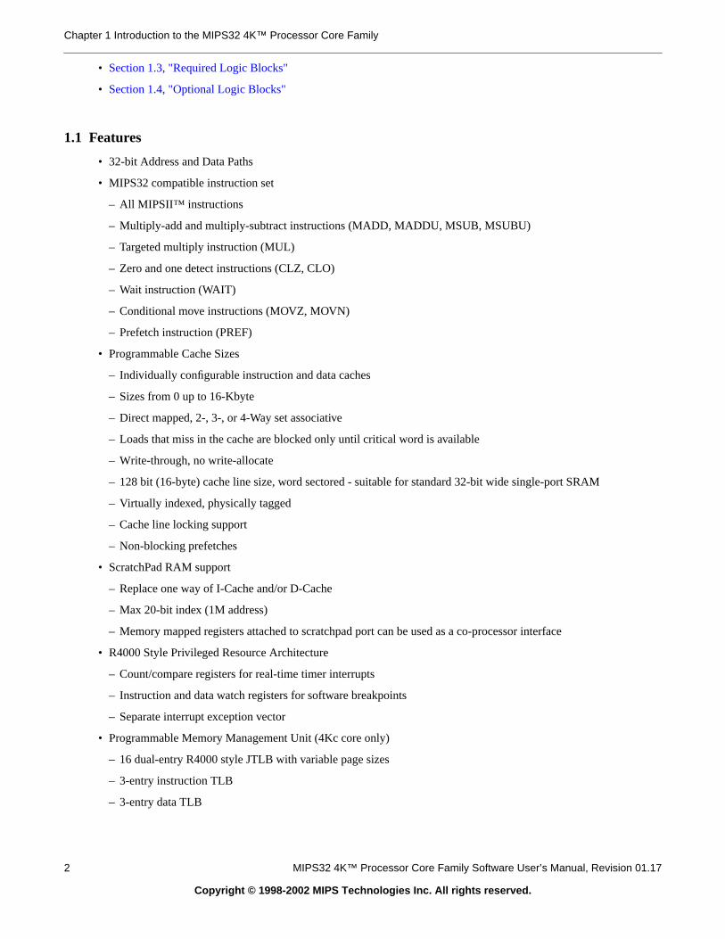
All cores contain both required and optional blocks. Required blocks are the lightly shaded areas of the block dand must be implemented to remain MIPS-compliant. Optional blocks can be added to the cores based on the nthe implementation. The required blocks are as follows:
• Execution Unit
• Multiply-Divide Unit (MDU)
• System Control Coprocessor (CP0)
• Memory Management Unit (MMU)
• Cache Controller
• Bus Interface Unit (BIU)
• Power Management
Optional blocks include:
• Instruction Cache (I-Cache)
MIPS32 4K™ Processor Core Family Software User’s Manual, Revision 01.17 3
Copyright © 1998-2002 MIPS Technologies Inc. All rights reserved.
Chapter 1 Introduction to the MIPS32 4K™ Processor Core Family
ide
tions
two read
ns are
• Data Cache (D-Cache)
• Enhanced JTAG (EJTAG) Controller
Figure 1-1 shows a block diagram of a 4K core. The MMU can be implemented using either a translation lookasbuffer (TLB) in the case of the 4Kc core, or a fixed mapping (FM) in the case of the 4Km and 4Kp cores. Refer toChapter3, “Memory Management,” on page 31 for more information.
Figure 1-1 4K Processor Core Block Diagram
1.3 Required Logic Blocks
The following subsections describe the various required logic blocks of the 4K processor cores.
1.3.1 Execution Unit
The core execution unit implements a load-store architecture with single-cycle Arithmetic Logic Unit (ALU) opera(logical, shift, add, subtract) and an autonomous multiply-divide unit. The core contains thirty-two 32-bitgeneral-purpose registers used for scalar integer operations and address calculation. The register file consists ofports and one write port and is fully bypassed to minimize operation latency in the pipeline.
The execution unit includes:
• 32-bit adder used for calculating the data address
• Address unit for calculating the next instruction address
• Logic for branch determination and branch target address calculation
• Load aligner
• Bypass multiplexers used to avoid stalls when executing instruction streams where data-producing instructiofollowed closely by consumers of their results
• Zero/One detect unit for implementing the CLZ and CLO instructions
• ALU for performing bitwise logical operations
SystemCoprocessor
CacheController
MDU
TLB or FM
MMU
D-Cache
BIU
TAP
EJTAG
PowerMgmt
I-Cache Off-ChipDebug I/F
Fixed/Required Optional
ExecutionCore
(RF/ALU/Shift
Thi
n I/F
On-
Chi
p B
us(e
s)
4 MIPS32 4K™ Processor Core Family Software User’s Manual, Revision 01.17
Copyright © 1998-2002 MIPS Technologies Inc. All rights reserved.

1.3 Required Logic Blocks
istsl6x16.ationsplete.skipses a
LO),ns. Itntedt to
ion is
t beion,
e
s andre
ede), and debug
after
three
areslatingused to
• Shifter and Store aligner
1.3.2 Multiply/Divide Unit (MDU)
The Multiply/Divide unit performs multiply and divide operations. In the 4Kc and 4Km processors, the MDU consof a 32x16 booth-encoded multiplier, result-accumulation registers (HI and LO), a divide state machine, and almultiplexers and control logic required to perform these functions. This pipelined MDU supports execution of a 1or 32x16 multiply operation every clock cycle; 32x32 multiply operations can be issued every other clock cycleAppropriate interlocks are implemented to stall the issue of back-to-back 32x32 multiply operations. Divide operare implemented with a simple 1 bit per clock iterative algorithm and require 35 clock cycles in worst case to comEarly-in to the algorithm detects sign extension of the dividend, if it is actual size is 24, 16 or 8 bit. the divider will7, 15 or 23 of the 32 iterations. An attempt to issue a subsequent MDU instruction while a divide is still active caupipeline stall until the divide operation is completed.
In the 4Kp processor, the non-pipelined MDU consists of a 32-bit full-adder, result-accumulation registers (HI anda combined multiply/divide state machine, and all multiplexers and control logic required to perform these functioperforms any multiply using 32 cycles in an iterative 1 bit per clock algorithm. Divide operations are also implemewith a simple 1 bit per clock iterative algorithm (no early-in) and require 35 clock cycles to complete. An attempissue a subsequent MDU instruction while a multiply/divide is still active causes a pipeline stall until the operatcompleted.
An additional multiply instruction, MUL is implemented, which specifies that the lower 32 bits of the multiply resulplaced in the register file instead of the HI/LO register pair. By avoiding the explicit move from LO (MFLO) instructrequired when using the LO register, and by supporting multiple destination registers, the throughput ofmultiply-intensive operations is increased.
Two instructions, multiply-add (MADD/MADDU) and multiply-subtract (MSUB/MSUBU), are used to perform thmultiply-add and multiply-subtract operations. The MADD instruction multiplies two numbers and then adds theproduct to the current contents of the HI and LO registers. Similarly, the MSUB instruction multiplies two operandthen subtracts the product from the HI and LO registers. The MADD/MADDU and MSUB/MSUBU operations acommonly used in Digital Signal Processor (DSP) algorithms.
1.3.3 System Control Coprocessor (CP0)
In the MIPS architecture, CP0 is responsible for the virtual-to-physical address translation, cache protocols, thexception control system, the processor’s diagnostics capability, operating mode selection (kernel vs. user mothe enabling/disabling of interrupts. Configuration information such as cache size, set associativity, and EJTAGfeatures are available by accessing the CP0 registers. Refer toChapter 5, “CP0 Registers,” on page 73 for moreinformation on the CP0 registers. Refer toChapter 9, “EJTAG Debug Support,” on page 121 for more information onEJTAG debug registers.
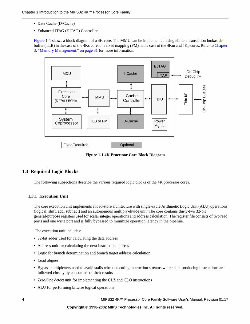
1.3.4 Memory Management Unit (MMU)
Each The core contains an MMU that interfaces between the execution unit and the cache controller, shown inFigure1-1. Although the 4Kc core implements a 32-bit architecture, the Memory Management Unit (MMU) is modeledthe MMU found in the 64-bit R4000 family, as defined by the MIPS32 architecture.
The 4Kc core implements an MMU based on a Translation Lookaside Buffer (TLB). The TLB actually consists oftranslation buffers: a 16 dual-entry fully associative Joint TLB (JTLB), a 3-entry fully associative Instruction TLB(ITLB) and a 3-entry fully associative data TLB(DTLB). The ITLB and DTLB, also referred to as the micro TLBs,managed by the hardware and are not software visible. The micro TLBs contain subsets of the JTLB. When tranaddresses, the corresponding micro TLB (I or D) is accessed first. If there is not a matching entry, the JTLB is
MIPS32 4K™ Processor Core Family Software User’s Manual, Revision 01.17 5
Copyright © 1998-2002 MIPS Technologies Inc. All rights reserved.
Chapter 1 Introduction to the MIPS32 4K™ Processor Core Family
imize a 1
TLB,ual
translate the address and refill the micro TLB. If the entry is not found in the JTLB, an exception is taken. To minthe micro TLB miss penalty, the JTLB is looked up in parallel with the DTLB for data references. This results incycle stall for a DTLB miss and a 2 cycle stall for an ITLB miss.
The 4Km and 4Kp cores implement an FM-based MMU instead of a TLB-based MMU. The FM replaces both the JITLB and DTLB in the 4Kc core. The FM performs a simple translation to get the physical address from the virtaddress. Refer toChapter 3, “Memory Management,” on page 31 for more information on the FM.
Figure 1-2shows how the ITLB, DTLB and JTLB are used in the 4Kc core.Figure 1-3show how the FM is used in the4Km and 4Kp cores.
Figure 1-2 Address Translation during a Cache Access in the 4Kc Core
I-Cache
D-Cache
Comparator
Comparator
InstructionHit/Miss
DataHit/Miss
Virtual Address
Virtual Address
ITLB
JTLB
DTLB
InstructionAddress
Calculator
DataAddress
Calculator
Entry
EntryIVA
6 MIPS32 4K™ Processor Core Family Software User’s Manual, Revision 01.17
Copyright © 1998-2002 MIPS Technologies Inc. All rights reserved.

1.3 Required Logic Blocks
. ForKbytes
cache,
of athem
rstalling
lock ofer
ent, andhe rest
Figure 1-3 Address Translation during a Cache Access in the 4Km and 4Kp Cores
1.3.5 Cache Controllers
The data and instruction cache controllers support caches of various sizes, organizations, and set associativityexample, the data cache can be 2 Kbytes in size and 2-way set associative, while the instruction cache can be 8in size and 4-way set associative. There are separate cache controllers for the I-Cache and D-Cache.
Each cache controller contains and manages a one-line fill buffer. Besides accumulating data to be written to thethe fill buffer is accessed in parallel with the cache and data can be bypassed back to the core.
Refer toChapter 7, “Caches,” on page 115 for more information on the instruction and data cache controllers.
1.3.6 Bus Interface Unit (BIU)
The Bus Interface Unit (BIU) controls the external interface signals. Additionally, it contains the implementation32-byte collapsing write-buffer. The purpose of this buffer is to hold and combine write transactions before issuingto the external interface. Since the data caches for all cores follow a write-through cache policy, the write-buffesignificantly reduces the number of write transactions on the external interface as well as reducing the amount ofin the core due to issuance of multiple writes in a short period of time.
The write-buffer is organized as two 16-byte buffers. Each buffer contains data from a single 16-byte aligned bmemory. One buffer contains the data currently being transferred on the external interface, while the other buffcontains accumulating data from the core.
1.3.7 Power Management
The core offers a number of power management features, including low-power design, active power managempower-down modes of operation. The core is a static design that supports a WAIT instruction designed to signal t
I-Cache
D-Cache
Comparator
Comparator
InstructionHit/Miss
DataHit/Miss
Virtual Address
Virtual Address
FM
InstructionAddress
Calculator
DataAddress
Calculator
MIPS32 4K™ Processor Core Family Software User’s Manual, Revision 01.17 7
Copyright © 1998-2002 MIPS Technologies Inc. All rights reserved.

Chapter 1 Introduction to the MIPS32 4K™ Processor Core Family
idle
controlode. In
nd rather, a lock
r-line”vailablet) on a
ysicallyolds 22
ructiont be
er-entry
uction
of the device that execution and clocking should be halted, hence reducing system power consumption during periods.
The core provides two mechanisms for system-level, low-power support:
• Register-controlled power management
• Instruction-controlled power management
In register controlled power management mode the core provides three bits in the CP0 Status register for softwareof the power management function and allows interrupts to be serviced even when the core is in power-down minstruction controlled power-down mode execution of the WAIT instruction is used to invoke low-power mode.
Refer toChapter 8, “Power Management,” on page 119 for more information on power management.
1.4 Optional Logic Blocks
The core consists of the following optional logic blocks as shown in the block diagram inFigure 1-1.
1.4.1 Instruction Cache
The instruction cache is an optional on-chip memory array of up to 16 Kbytes. The cache is virtually indexed aphysically tagged, allowing the virtual-to-physical address translation to occur in parallel with the cache accessthan having to wait for the physical address translation. The tag holds 22 bits of the physical address, 4 valid bitsbit, and the LRF (Least Recently Filled) replacement bit.
All cores support instruction cache-locking. Cache locking allows critical code to be locked into the cache on a “pebasis, enabling the system designer to maximize the efficiency of the system cache. Cache locking is always aon all instruction cache entries. Entries can be marked as locked or unlocked (by setting or clearing the lock-biper-entry basis using the CACHE instruction.
1.4.2 Data Cache
The data cache is an optional on-chip memory array of up to 16-Kbytes. The cache is virtually indexed and phtagged, allowing the virtual-to-physical address translation to occur in parallel with the cache access. The tag hbits of the physical address, 4 valid bits, a lock bit, and the LRF replacement bit.
In addition to instruction cache locking, all cores also support a data cache locking mechanism identical to the instcache, with critical data segments to be locked into the cache on a “per-line” basis. The locked contents cannoselected for replacement on a cache miss, but can be updated on a store hit.
Cache locking is always available on all data cache entries. Entries can be marked as locked or unlocked on a pbasis using the CACHE instruction.
The physical data cache memory must be byte writable to support non-word store operations.
1.4.3 EJTAG Controller
All cores provide basic EJTAG support with debug mode, run control, single step and software breakpoint instr(SDBBP) as part of the core. These features allow for the basic software debug of user and kernel code.
8 MIPS32 4K™ Processor Core Family Software User’s Manual, Revision 01.17
Copyright © 1998-2002 MIPS Technologies Inc. All rights reserved.

1.4 Optional Logic Blocks
o data
virtualeakpoints
h virtualompare,
a in the
Optional EJTAG features include hardware breakpoints. A 4K core may have four instruction breakpoints and twbreakpoints, two instruction breakpoints and one data breakpoint, or no breakpoints. The hardware instructionbreakpoints can be configured to generate a debug exception when an instruction is executed anywhere in theaddress space. Bit mask and address space identifier (ASID) values may apply in the address compare. These brare not limited to code in RAM like the software instruction breakpoint (SDBBP). The data breakpoints can beconfigured to generate a debug exception on a data transaction. The data transaction may be qualified with botaddress, data value, size and load/store transaction type. Bit mask and ASID values may apply in the address cand byte mask may apply in the value compare.
Refer toChapter 9, “EJTAG Debug Support,” on page 121 for more information on hardware breakpoints.
An optional Test Access Port (TAP) provides for the communication from an EJTAG probe to the CPU throughdedicated port, may also be applied to the core. This provides the possibility for debugging without debug codeapplication, and for download of application code to the system.
Refer toChapter 9, “EJTAG Debug Support,” on page 121 for more information on the EJTAG features.
MIPS32 4K™ Processor Core Family Software User’s Manual, Revision 01.17 9
Copyright © 1998-2002 MIPS Technologies Inc. All rights reserved.
Chapter 1 Introduction to the MIPS32 4K™ Processor Core Family
10 MIPS32 4K™ Processor Core Family Software User’s Manual, Revision 01.17
Copyright © 1998-2002 MIPS Technologies Inc. All rights reserved.

lineer
Chapter 2
Pipeline
The MIPS32 4K processor cores implements a 5-stage pipeline similar to the original R3000 pipeline. The pipeallows the processor to achieve high frequency while minimizing device complexity, reducing both cost and powconsumption. This chapter contains the following sections:
• Section 2.1, "Pipeline Stages"
• Section 2.2, "Instruction Cache Miss"
• Section 2.3, "Data Cache Miss"
• Section 2.4, "Multiply/Divide Operations"
• Section 2.5, "MDU Pipeline (4Kc and 4Km Cores)"
• Section 2.6, "MDU Pipeline (4Kp Core Only)"
• Section 2.7, "Branch Delay"
• Section 2.8, "Data Bypassing"
• Section 2.9, "Interlock Handling"
• Section 2.10, "Slip Conditions"
• Section 2.11, "Instruction Interlocks"
• Section 2.12, "Instruction Hazards"
2.1 Pipeline Stages
The pipeline consists of five stages:
• Instruction (I stage)
• Execution (E stage)
• Memory (M stage)
• Align/Accumulate (A stage)
• Writeback (W stage)
All three cores implement a “Bypass” mechanism that allows the result of an operation to be sent directly to theinstruction that needs it without having to write the result to the register and then read it back.
Figure 2-1 shows the operations performed in each pipeline stage of the 4Kc processor.
MIPS32 4K™ Processor Core Family Software User’s Manual, Revision 01.17 11
Copyright © 1998-2002 MIPS Technologies Inc. All rights reserved.

Chapter 2 Pipeline
Figure 2-1 4Kc Core Pipeline Stages
Figure 2-2 shows the operations performed in each pipeline stage of the 4Km processor core.
Figure 2-2 4Km Core Pipeline Stages
Figure 2-3 shows the operations performed in each pipeline stage of the 4Kp processor core.
Figure 2-3 4Kp Core Pipeline Stages
I
A->E BypassM->E Bypass
A->E Bypass
E M A W
I-Cache
I-TLB
RegRd
I Dec D-AC
I-AC1 I-AC2
ALU Op
D-Cache
D-TLB
Align
MUL RegWRegW
RegW
RegW
RegW
Mult, Macc 16x16, 32x16 CPA
CPAMult, Macc 32x32
Sign AdjustDivide
IU-P
ipe
line
MD
U-P
ipe
line
I-AC2
D-AC
Align
MUL
I-TLB
I Dec
ALU Op
D-Cache
D-TLB
Divide
Mult, Macc
Sign Adjust
I-Cache
RegRd
I-AC1
RegW
CPA
: I$ Tag and Data read: I-TLB Look-up: Instruction Decode: Register file read: Instruction Address Calculation stage 1 and 2: Arithmetic Logic and Shift operations: Data Address Calculation: D$ Tag and Data read: D-TLB Look-up: Load data aligner: Register file write or HI/LO write: The MUL instruction. Uses MDU-Pipeline write Reg file: Carry Propagate Adder: Multiply and Multiply Accumulate instructions: Divide instructions: Last stage of Divide is a sign adjustment
: One or more stall cycles.
I
A->E BypassM->E Bypass
A->E Bypass
E M A W
I-Cache RegRd
I Dec D-AC
I-AC1 I-AC2
ALU Op
D-Cache Align
MUL
RegW
RegW
RegW
RegW
RegW
Mult, Macc 16x16, 32x16Carry Prop. Add
Carry Prop. AddMult, Macc 32x32
Sign AdjustDivide
RegW
I-AC2
D-AC
Align
MUL
I Dec
ALU Op
D-Cache
Divide
Mult, Macc
Sign Adjust
I-Cache
RegRd
I-AC1
CPA
: I$ Tag and Data read: Instruction Decode: Register file read: Instruction Address Calculation stage 1 and 2: Arithmetic Logic and Shift operations: Data Address Calculation: D$ Tag and Data read: Load data aligner: Register file write or HI/LO write: The MUL instruction. Uses MDU-Pipeline write Reg file: Carry Propagate Adder: Multiply and Multiply Accumulate instructions: Divide instructions: Last stage of Divide is a sign adjustment
: One or more stall cycles.
IU-P
ipe
line
MD
U-P
ipe
line
I
A->E BypassM->E Bypass
A->E Bypass
E M A W
I-Cache
I-TLB
RegRd
I Dec D-AC
I-AC1 I-AC2
ALU Op
D-Cache
D-TLB
Align
MUL
RegW
RegW
RegWMultiply, Divide
RegW
I-AC2
D-AC
Align
MUL
I Dec
ALU Op
D-Cache
Multiply, Divide
I-Cache
RegRd
I-AC1
: I$ Tag and Data read: Instruction Decode: Register file read: Instruction Address Calculation stage 1 and 2: Arithmetic Logic and Shift operations: Data Address Calculation: D$ Tag and Data read: Load data aligner: Register file write or HI/LO write: The MUL instruction. Uses MDU-Pipeline, write Reg file: Multiply, Multiply Accumulate and Divide instructions
: One or more stall cycles.
IU-P
ipe
line
MD
U-P
ipe
line
12 MIPS32 4K™ Processor Core Family Software User’s Manual, Revision 01.17
Copyright © 1998-2002 MIPS Technologies Inc. All rights reserved.

2.1 Pipeline Stages
branch
ructions.
the
.
2.1.1 I Stage: Instruction Fetch
During the Instruction fetch stage:
• An instruction is fetched from the instruction cache.
• The I-TLB performs a virtual-to-physical address translation (4Kc core only).
2.1.2 E Stage: Execution
During the Execution stage:
• Operands are fetched from the register file.
• Operands from M and A stage are bypassed to this stage.
• The Arithmetic Logic Unit (ALU) begins the arithmetic or logical operation for register-to-register instructions.
• The ALU calculates the data virtual address for load and store instructions.
• The ALU determines whether the branch condition is true and calculates the virtual branch target address forinstructions.
• Instruction logic selects an instruction address
• All multiply and divide operations begin in this stage.
2.1.3 M Stage: Memory Fetch
During the Memory Fetch stage:
• The arithmetic or logic ALU operation completes.
• The data cache fetch and the data virtual-to-physical address translation are performed for load and store inst
• Data TLB (4Kc core only) and data cache lookup are performed and a hit/miss determination is made.
• A 16x16 or 32x16 MUL operation completes in the array and stalls for one clock in the M stage to complete carry-propagate-add in the M stage (4Kc and 4Km cores).
• A 32x32 MUL operation stalls for two clocks in the M stage to complete second cycle of the array and thecarry-propagate-add in the M stage (4Kc and 4Km cores).
• A 16x16 or 32x16 MULT/MADD/MSUB operation completes in the array (4Kc and 4Km cores).
• A 32x32 MULT/MADD/MSUB operation stalls for one clock in the MMDU stage of the MDU pipeline to completesecond cycle in the array (4Kc and 4Km cores).
• A divide operation stalls for a maximum of 32 clocks in the MMDU stage of the MDU pipeline (4Kc and 4Km cores)
• A multiply operation stalls for 31 clocks in MMDU stage (4Kp core only).
• A multiply-accumulate operation stalls for 33 clocks in MMDU stage (4Kp core only).
• A divide operation stalls for 32 clocks in the MMDU stage (4Kp core only).
2.1.4 A Stage: Align/Accumulate
During the Align/Accumulate stage:
• A separate aligner aligns loaded data with its word boundary.
MIPS32 4K™ Processor Core Family Software User’s Manual, Revision 01.17 13
Copyright © 1998-2002 MIPS Technologies Inc. All rights reserved.
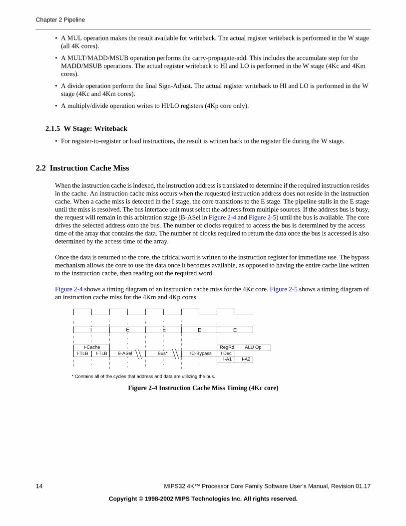
Chapter 2 Pipeline
stage
eKm
he W
residestructionE stageis busy,
e accessd is also
bypasse written
• A MUL operation makes the result available for writeback. The actual register writeback is performed in the W(all 4K cores).
• A MULT/MADD/MSUB operation performs the carry-propagate-add. This includes the accumulate step for thMADD/MSUB operations. The actual register writeback to HI and LO is performed in the W stage (4Kc and 4cores).
• A divide operation perform the final Sign-Adjust. The actual register writeback to HI and LO is performed in tstage (4Kc and 4Km cores).
• A multiply/divide operation writes to HI/LO registers (4Kp core only).
2.1.5 W Stage: Writeback
• For register-to-register or load instructions, the result is written back to the register file during the W stage.
2.2 Instruction Cache Miss
When the instruction cache is indexed, the instruction address is translated to determine if the required instructionin the cache. An instruction cache miss occurs when the requested instruction address does not reside in the inscache. When a cache miss is detected in the I stage, the core transitions to the E stage. The pipeline stalls in theuntil the miss is resolved. The bus interface unit must select the address from multiple sources. If the address busthe request will remain in this arbitration stage (B-ASel inFigure 2-4andFigure 2-5) until the bus is available. The coredrives the selected address onto the bus. The number of clocks required to access the bus is determined by thtime of the array that contains the data. The number of clocks required to return the data once the bus is accessedetermined by the access time of the array.
Once the data is returned to the core, the critical word is written to the instruction register for immediate use. Themechanism allows the core to use the data once it becomes available, as opposed to having the entire cache linto the instruction cache, then reading out the required word.
Figure 2-4shows a timing diagram of an instruction cache miss for the 4Kc core.Figure 2-5shows a timing diagram ofan instruction cache miss for the 4Km and 4Kp cores.
Figure 2-4 Instruction Cache Miss Timing (4Kc core)
EEE EI
I DecI-Cache
I-TLB I-TLB B-ASel Bus* IC-BypassRegRd ALU Op
I-A2I-A1
* Contains all of the cycles that address and data are utilizing the bus.
14 MIPS32 4K™ Processor Core Family Software User’s Manual, Revision 01.17
Copyright © 1998-2002 MIPS Technologies Inc. All rights reserved.
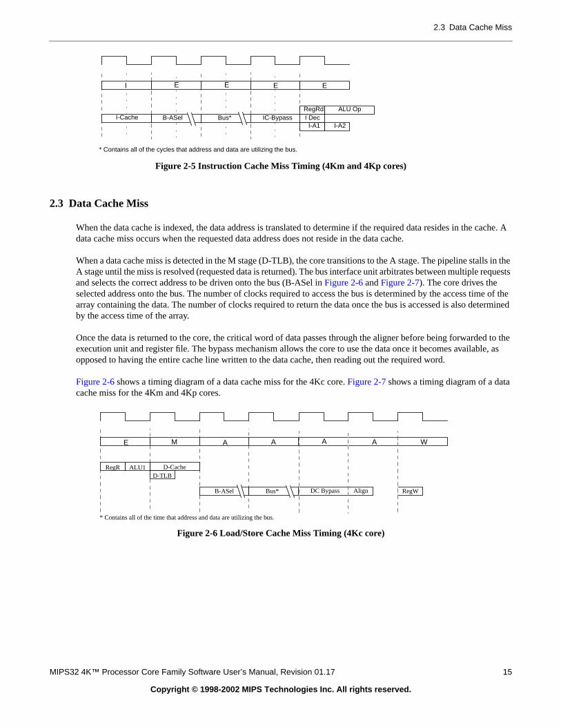
2.3 Data Cache Miss
cache. A
s in theequests
ime of thetermined
d to theble, as
Figure 2-5 Instruction Cache Miss Timing (4Km and 4Kp cores)
2.3 Data Cache Miss
When the data cache is indexed, the data address is translated to determine if the required data resides in thedata cache miss occurs when the requested data address does not reside in the data cache.
When a data cache miss is detected in the M stage (D-TLB), the core transitions to the A stage. The pipeline stallA stage until the miss is resolved (requested data is returned). The bus interface unit arbitrates between multiple rand selects the correct address to be driven onto the bus (B-ASel inFigure 2-6 andFigure 2-7). The core drives theselected address onto the bus. The number of clocks required to access the bus is determined by the access tarray containing the data. The number of clocks required to return the data once the bus is accessed is also deby the access time of the array.
Once the data is returned to the core, the critical word of data passes through the aligner before being forwardeexecution unit and register file. The bypass mechanism allows the core to use the data once it becomes availaopposed to having the entire cache line written to the data cache, then reading out the required word.
Figure 2-6shows a timing diagram of a data cache miss for the 4Kc core.Figure 2-7shows a timing diagram of a datacache miss for the 4Km and 4Kp cores.
Figure 2-6 Load/Store Cache Miss Timing (4Kc core)
EEE EI
I DecI-Cache B-ASel Bus* IC-BypassRegRd ALU Op
I-A2I-A1
* Contains all of the cycles that address and data are utilizing the bus.
D-TLBD-CacheALU1
B-ASel
RegR
Bus* RegWAlignDC Bypass
* Contains all of the time that address and data are utilizing the bus.
WAAAAME
MIPS32 4K™ Processor Core Family Software User’s Manual, Revision 01.17 15
Copyright © 1998-2002 MIPS Technologies Inc. All rights reserved.

Chapter 2 Pipeline
fileand
tions.e HIt fromms.
thellowinge usedDU
fort stallby
tee
pass
canx32ons the
Figure 2-7 Load/Store Cache Miss Timing (4Km and 4Kp cores)
2.4 Multiply/Divide Operations
All three cores implement the standard MIPS II™ multiply and divide instructions. Additionally, several newinstructions were added for enhanced performance.
The targeted multiply instruction, MUL, specifies that multiply results be placed in the general purpose registerinstead of the HI/LO register pair. By avoiding the explicit MFLO instruction, required when using the LO register,by supporting multiple destination registers, the throughput of multiply-intensive operations is increased.
Four instructions, multiply-add (MADD), multiply-add-unsigned (MADDU) multiply-subtract (MSUB), andmultiply-subtract-unsigned (MSUBU), are used to perform the multiply-accumulate and multiply-subtract operaThe MADD/MADDU instruction multiplies two numbers and then adds the product to the current contents of thand LO registers. Similarly, the MSUB/MSUBU instruction multiplies two operands and then subtracts the producthe HI and LO registers. The MADD/MADDU and MSUB/MSUBU operations are commonly used in DSP algorith
All multiply operations (except the MUL instruction) write to the HI/LO register pair. All integer operations write togeneral purpose registers (GPR). Because MDU operations write to different registers than integer operations, fointeger instructions can execute before the MDU operation has completed. The MFLO and MFHI instructions arto move data from the HI/LO register pair to the GPR file. If a MFLO or MFHI instruction is issued before the Moperation completes, it will stall to wait for the data.
2.5 MDU Pipeline (4Kc and 4Km Cores)
The 4Kc and 4Km processor cores contain an autonomous multiply/divide unit (MDU) with a separate pipelinemultiply and divide operations. This pipeline operates in parallel with the integer unit (IU) pipeline and does nowhen the IU pipeline stalls. This allows long-running MDU operations, such as a divide, to be partially masked system stalls and/or other integer unit instructions.
The MDU consists of a 32x16 booth encoded multiplier, result/accumulation registers (HI and LO), a divide stamachine, and all necessary multiplexers and control logic. The first number shown (‘32’ of 32x16) represents thrsoperand. The second number (‘16’ of 32x16) represents thert operand. The core only checks the latter(rt) operand valueto determine how many times the operation must pass through the multiplier. The 16x16 and 32x16 operationsthrough the multiplier once. A 32x32 operation passes through the multiplier twice.
The MDU supports execution of a 16x16 or 32x16 multiply operation every clock cycle; 32x32 multiply operationsbe issued every other clock cycle. Appropriate interlocks are implemented to stall the issue of back-to-back 32multiply operations. Multiply operand size is automatically determined by logic built into the MDU. Divide operatiare implemented with a simple 1 bit per clock iterative algorithm with an early in detection of sign extension on
D-CacheALU1
B-ASel
RegR
Bus* RegWAlignDC Bypass
* Contains all of the time that address and data are utilizing the bus.
WAAAAME
16 MIPS32 4K™ Processor Core Family Software User’s Manual, Revision 01.17
Copyright © 1998-2002 MIPS Technologies Inc. All rights reserved.
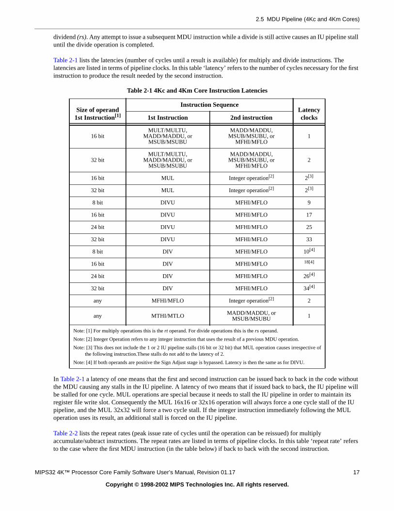
2.5 MDU Pipeline (4Kc and 4Km Cores)
stall
e first
ithoutwill
in itse IU
’ refers
dividend(rs). Any attempt to issue a subsequent MDU instruction while a divide is still active causes an IU pipelineuntil the divide operation is completed.
Table 2-1 lists the latencies (number of cycles until a result is available) for multiply and divide instructions. Thelatencies are listed in terms of pipeline clocks. In this table ‘latency’ refers to the number of cycles necessary for thinstruction to produce the result needed by the second instruction.
In Table 2-1a latency of one means that the first and second instruction can be issued back to back in the code wthe MDU causing any stalls in the IU pipeline. A latency of two means that if issued back to back, the IU pipelinebe stalled for one cycle. MUL operations are special because it needs to stall the IU pipeline in order to maintaregister file write slot. Consequently the MUL 16x16 or 32x16 operation will always force a one cycle stall of thpipeline, and the MUL 32x32 will force a two cycle stall. If the integer instruction immediately following the MULoperation uses its result, an additional stall is forced on the IU pipeline.
Table 2-2 lists the repeat rates (peak issue rate of cycles until the operation can be reissued) for multiplyaccumulate/subtract instructions. The repeat rates are listed in terms of pipeline clocks. In this table ‘repeat rateto the case where the first MDU instruction (in the table below) if back to back with the second instruction.
Table 2-1 4Kc and 4Km Core Instruction Latencies
Size of operand1st Instruction[1]
Instruction SequenceLatencyclocks1st Instruction 2nd instruction
16 bitMULT/MULTU,
MADD/MADDU, orMSUB/MSUBU
MADD/MADDU,MSUB/MSUBU, or
MFHI/MFLO1
32 bitMULT/MULTU,
MADD/MADDU, orMSUB/MSUBU
MADD/MADDU,MSUB/MSUBU, or
MFHI/MFLO2
16 bit MUL Integer operation[2] 2[3]
32 bit MUL Integer operation[2] 2[3]
8 bit DIVU MFHI/MFLO 9
16 bit DIVU MFHI/MFLO 17
24 bit DIVU MFHI/MFLO 25
32 bit DIVU MFHI/MFLO 33
8 bit DIV MFHI/MFLO 10[4]
16 bit DIV MFHI/MFLO 18[4]
24 bit DIV MFHI/MFLO 26[4]
32 bit DIV MFHI/MFLO 34[4]
any MFHI/MFLO Integer operation[2] 2
any MTHI/MTLO MADD/MADDU, orMSUB/MSUBU 1
Note: [1] For multiply operations this is thert operand. For divide operations this is thers operand.
Note: [2] Integer Operation refers to any integer instruction that uses the result of a previous MDU operation.
Note: [3] This does not include the 1 or 2 IU pipeline stalls (16 bit or 32 bit) that MUL operation causes irrespective ofthe following instruction.These stalls do not add to the latency of 2.
Note: [4] If both operands are positive the Sign Adjust stage is bypassed. Latency is then the same as for DIVU.
MIPS32 4K™ Processor Core Family Software User’s Manual, Revision 01.17 17
Copyright © 1998-2002 MIPS Technologies Inc. All rights reserved.

Chapter 2 Pipeline
cks in
e MDU MDU
are
thepeline
Figure 2-8 below shows the pipeline flow for the following sequence:
1. 32x16 multiply (Mult1)
2. Add
3. 32x32 multiply (Mult2)
4. Sub
The 32x16 multiply operation requires one clock of each pipeline stage to complete. The 32x32 requires two clothe MMDU pipe-stage. The MDU pipeline is shown as the shaded areas ofFigure 2-8and always starts a computation inthe final phase of the E stage. As shown in the figure, the MMDU pipe-stage of the MDU pipeline occurs in parallel withthe M stage of the IU pipeline, the AMDU stage occurs in parallel with the A stage, and the WMDU stage occurs in parallelwith the W stage. However in case the instruction in the MDU pipeline needs multiple passes through the samstage, this parallel behavior will be skewed by one or more clocks. This is not a problem because results in thepipeline are written to HI and LO registers, while the integer pipeline results are written to the register file.
Figure 2-8 MDU Pipeline Behavior during Multiply Operations (4Kc and 4Km processors)
The following is a cycle-by-cycle analysis ofFigure 2-8.
1. The first 32x16 multiply operation (Mult1) enters the I stage and is fetched from the instruction cache.
2. An Add operation enters the I stage. The Mult1 operation enters the E stage. The integer and MDU pipelines shthe I and E pipeline stages. At the end of the E stage in cycle 2, the multiply operation (Mult1) is passed to theMDU pipeline.
3. In cycle 3 a 32x32 multiply operation (Mult2) enters the I stage and is fetched from the instruction cache. SinceAdd operation has not yet reached the M stage by cycle 3, there is no activity in the M stage of the integer piat this time.
4. In cycle 4 the Sub instruction enters I stage. The second multiply operation (Mult2) enters the E stage. And the Addoperation enters M stage of the integer pipe. Since the Mult1 multiply is a 32x16 operation, only one clock isrequired for the MMDU stage, hence the Mult1 operation passes to the AMDU stage of the MDU pipeline.
Table 2-2 4Kc and 4Km Core Instruction Repeat Rates
Operand Size of1st Instruction
Instruction SequenceRepeatRate1st Instruction 2nd instruction
16 bitMULT/MULTU,
MADD/MADDU,MSUB/MSUBU
MADD/MADDU,MSUB/MSUBU 1
32 bitMULT/MULTU,
MADD/MADDU,MSUB/MSUBU
MADD/MADDU,MSUB/MSUBU 2
I E A WM
cycle 1 cycle 2 cycle 3 cycle 4 cycle 5 cycle 6 cycle 7 cycle 8
Mult1
Add
Mult2
I E AMDU WMDUMMDU
I E AMDU WMDUMMDUMMDU
Sub
I E A WM
18 MIPS32 4K™ Processor Core Family Software User’s Manual, Revision 01.17
Copyright © 1998-2002 MIPS Technologies Inc. All rights reserved.
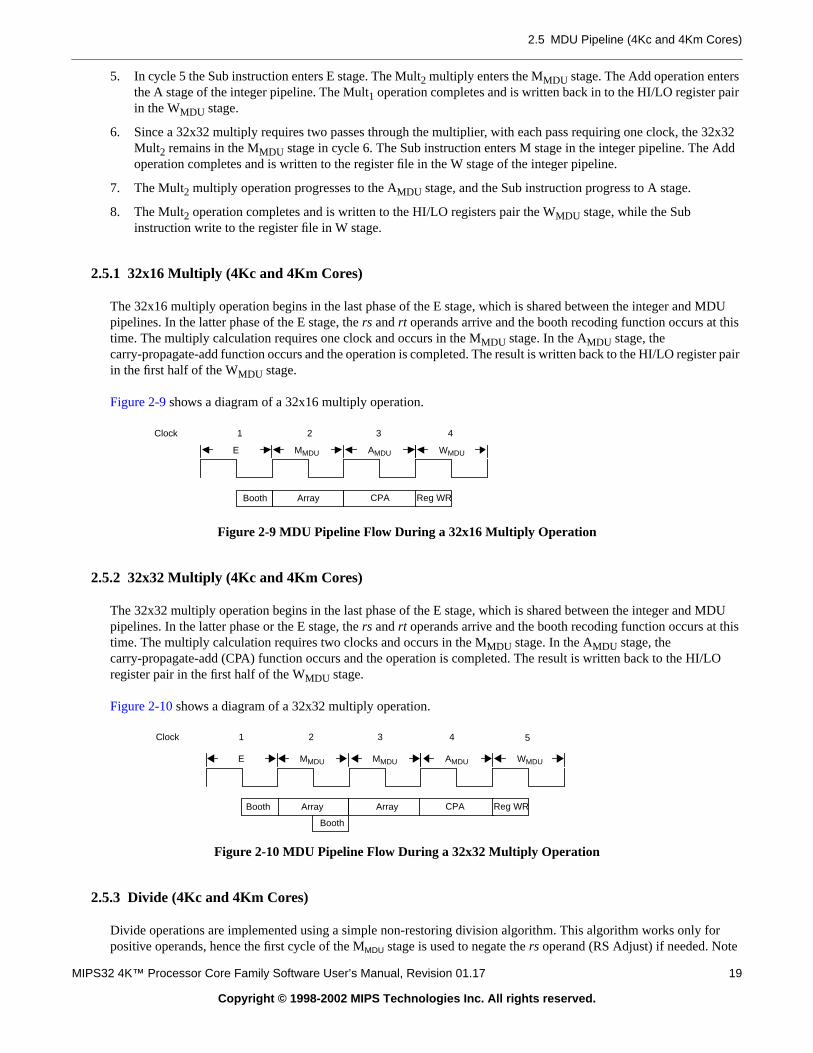
2.5 MDU Pipeline (4Kc and 4Km Cores)
ir
32x32Add
MDUis
ter pair
MDUis
/LO
or
5. In cycle 5 the Sub instruction enters E stage. The Mult2 multiply enters the MMDU stage. The Add operation entersthe A stage of the integer pipeline. The Mult1 operation completes and is written back in to the HI/LO register pain the WMDU stage.
6. Since a 32x32 multiply requires two passes through the multiplier, with each pass requiring one clock, the Mult2 remains in the MMDU stage in cycle 6. The Sub instruction enters M stage in the integer pipeline. The operation completes and is written to the register file in the W stage of the integer pipeline.
7. The Mult2 multiply operation progresses to the AMDU stage, and the Sub instruction progress to A stage.
8. The Mult2 operation completes and is written to the HI/LO registers pair the WMDU stage, while the Subinstruction write to the register file in W stage.
2.5.1 32x16 Multiply (4Kc and 4Km Cores)
The 32x16 multiply operation begins in the last phase of the E stage, which is shared between the integer andpipelines. In the latter phase of the E stage, thers andrt operands arrive and the booth recoding function occurs at thtime. The multiply calculation requires one clock and occurs in the MMDU stage. In the AMDU stage, thecarry-propagate-add function occurs and the operation is completed. The result is written back to the HI/LO regisin the first half of the WMDU stage.
Figure 2-9 shows a diagram of a 32x16 multiply operation.
Figure 2-9 MDU Pipeline Flow During a 32x16 Multiply Operation
2.5.2 32x32 Multiply (4Kc and 4Km Cores)
The 32x32 multiply operation begins in the last phase of the E stage, which is shared between the integer andpipelines. In the latter phase or the E stage, thers andrt operands arrive and the booth recoding function occurs at thtime. The multiply calculation requires two clocks and occurs in the MMDU stage. In the AMDU stage, thecarry-propagate-add (CPA) function occurs and the operation is completed. The result is written back to the HIregister pair in the first half of the WMDU stage.
Figure 2-10 shows a diagram of a 32x32 multiply operation.
Figure 2-10 MDU Pipeline Flow During a 32x32 Multiply Operation
2.5.3 Divide (4Kc and 4Km Cores)
Divide operations are implemented using a simple non-restoring division algorithm. This algorithm works only fpositive operands, hence the first cycle of the MMDU stage is used to negate thers operand (RS Adjust) if needed. Note
Booth Array CPA
E MMDU AMDU
Reg WR
WMDU
Clock 1 2 3 4
Booth Array
E MMDU MMDU AMDU
Reg WR
WMDU
CPAArray
Booth
Clock 1 2 3 4 5
MIPS32 4K™ Processor Core Family Software User’s Manual, Revision 01.17 19
Copyright © 1998-2002 MIPS Technologies Inc. All rights reserved.

Chapter 2 Pipeline
ute aneing 7,
even ifhe sign
that this cycle is executed even if the adjustment is not necessary. At maximum the next 32 clocks (3-34) execiterative add/subtract function. In cycle 3 an early in detection is performed in parallel with the add/subtract. Thadjustedrs operand is detected to be zero extended on the upper most 8, 16 or 24 bits. If this is the case the follow15 or 23 cycles of the add/subtract iterations are skipped.
The remainder adjust (Rem Adjust) cycle is required if the remainder was negative. Note that this cycle is takenthe remainder was positive. A sign adjust is performed on the quotient and/or remainder if necessary. Note that tadjust cycle is skipped if both operands are positive. In this case the Rem Adjust is moved to the AMDU stage.
Figure 2-11, Figure 2-12, Figure 2-13 andFigure 2-14 show the latency for 8, 16, 24 and 32-bit divide operations,respectively. The repeat rate is either 11, 19, 27 or 35 cycles (one less if thesign adjust stage is skipped) as a seconddivide can be in theRS Adjust stage when the first divide is in theReg WR stage.
Figure 2-11 MDU Pipeline Flow During an 8-bit Divide (DIV) Operation
Figure 2-12 MDU Pipeline Flow During a 16-bit Divide (DIV) Operation
Figure 2-13 MDU Pipeline Flow During a 24-bit Divide (DIV) Operation
Figure 2-14 MDU Pipeline Flow During a 32-bit Divide (DIV) Operation
RS Adjust
E Stage MMDU Stage MMDU Stage MMDU Stage AMDU Stage
Rem AdjustAdd/Subtract
Clock 1 2 4-10 11 12
WMDU Stage
13
Reg WRSign Adjust
MMDU Stage
Add/Subtract
3
Early In
RS Adjust
E Stage MMDU Stage MMDU Stage MMDU Stage AMDU Stage
Rem AdjustAdd/Subtract
Clock 1 2 4-18 19 20
WMDU Stage
21
Reg WRSign Adjust
MMDU Stage
Add/Subtract
3
Early In
RS Adjust
E Stage MMDU Stage MMDU Stage MMDU Stage AMDU Stage
Rem AdjustAdd/Subtract
Clock 1 2 4-26 27 28
WMDU Stage
29
Reg WRSign Adjust
MMDU Stage
Add/Subtract
3
Early In
RS Adjust
E Stage MMDU Stage MMDU Stage MMDU Stage AMDU Stage
Rem AdjustAdd/Subtract
Clock 1 2 4-34 35 36
WMDU Stage
37
Reg WRSign Adjust
MMDU Stage
Add/Subtract
3
Early In
20 MIPS32 4K™ Processor Core Family Software User’s Manual, Revision 01.17
Copyright © 1998-2002 MIPS Technologies Inc. All rights reserved.
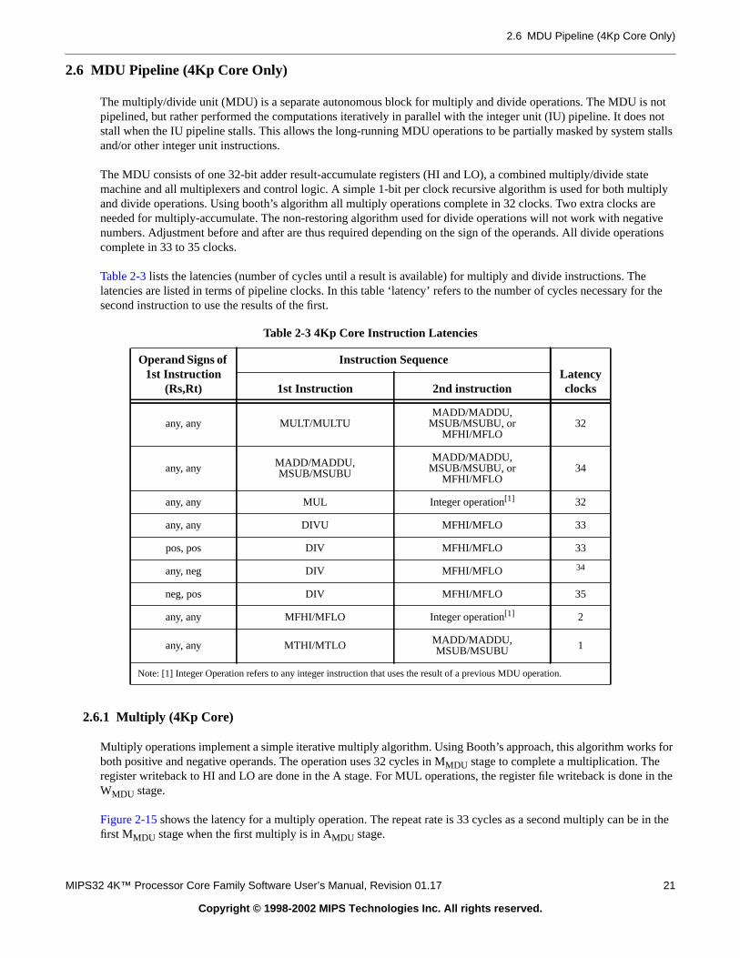
2.6 MDU Pipeline (4Kp Core Only)
not notstalls
teltiplyretiverations
r the
for
in the
in the
2.6 MDU Pipeline (4Kp Core Only)
The multiply/divide unit (MDU) is a separate autonomous block for multiply and divide operations. The MDU ispipelined, but rather performed the computations iteratively in parallel with the integer unit (IU) pipeline. It doesstall when the IU pipeline stalls. This allows the long-running MDU operations to be partially masked by systemand/or other integer unit instructions.
The MDU consists of one 32-bit adder result-accumulate registers (HI and LO), a combined multiply/divide stamachine and all multiplexers and control logic. A simple 1-bit per clock recursive algorithm is used for both muand divide operations. Using booth’s algorithm all multiply operations complete in 32 clocks. Two extra clocks aneeded for multiply-accumulate. The non-restoring algorithm used for divide operations will not work with neganumbers. Adjustment before and after are thus required depending on the sign of the operands. All divide opecomplete in 33 to 35 clocks.
Table 2-3 lists the latencies (number of cycles until a result is available) for multiply and divide instructions. Thelatencies are listed in terms of pipeline clocks. In this table ‘latency’ refers to the number of cycles necessary fosecond instruction to use the results of the first.
2.6.1 Multiply (4Kp Core)
Multiply operations implement a simple iterative multiply algorithm. Using Booth’s approach, this algorithm worksboth positive and negative operands. The operation uses 32 cycles in MMDU stage to complete a multiplication. Theregister writeback to HI and LO are done in the A stage. For MUL operations, the register file writeback is doneWMDU stage.
Figure 2-15 shows the latency for a multiply operation. The repeat rate is 33 cycles as a second multiply can befirst MMDU stage when the first multiply is in AMDU stage.
Table 2-3 4Kp Core Instruction Latencies
Operand Signs of1st Instruction
(Rs,Rt)
Instruction SequenceLatencyclocks1st Instruction 2nd instruction
any, any MULT/MULTUMADD/MADDU,
MSUB/MSUBU, orMFHI/MFLO
32
any, any MADD/MADDU,MSUB/MSUBU
MADD/MADDU,MSUB/MSUBU, or
MFHI/MFLO34
any, any MUL Integer operation[1] 32
any, any DIVU MFHI/MFLO 33
pos, pos DIV MFHI/MFLO 33
any, neg DIV MFHI/MFLO 34
neg, pos DIV MFHI/MFLO 35
any, any MFHI/MFLO Integer operation[1] 2
any, any MTHI/MTLO MADD/MADDU,MSUB/MSUBU 1
Note: [1] Integer Operation refers to any integer instruction that uses the result of a previous MDU operation.
MIPS32 4K™ Processor Core Family Software User’s Manual, Revision 01.17 21
Copyright © 1998-2002 MIPS Technologies Inc. All rights reserved.

Chapter 2 Pipeline
eeded.
ands,le isction.
r. Noteor if thisstck to
howt M
Figure 2-15 4Kp MDU Pipeline Flow During a Multiply Operation
2.6.2 Multiply Accumulate (4Kp Core)
Multiply-accumulate operations use the same multiply machine as used for multiply only. Two extra stages are nto perform the addition/subtraction. The operations uses 34 cycles in MMDU stage to complete the multiply-accumulateThe register writeback to HI and LO are done in the A stage.
Figure 2-16 shows the latency for a multiply-accumulate operation. The repeat rate is 35 cycles as a secondmultiply-accumulate can be in the E stage when the first multiply is in the last MMDU stage.
Figure 2-16 4Kp MDU Pipeline Flow During a Multiply Accumulate Operation
2.6.3 Divide (4Kp Core)
Divide operations also implement a simple non-restoring algorithm. This algorithm works only for positive operhence the first cycle of the MMDU stage is used to negate the rs operand (RS Adjust) if needed. Note that this cycexecuted even if negation is not needed. The next 32 cycle (3-34) executes an interactive add/subtract-shift fun
Two sign adjust (Sign Adjust 1/2) cycles are used to change the sign of one or both the quotient and the remaindethat one or both of these cycles are skipped if they are not needed. The rule is, if both operands were positive is an unsigned division; both of the sign adjust cycles are skipped. If thers operand was negative, one of the sign adjucycles is skipped. If only thers operand was negative, none of the sign adjust cycles are skipped. Register writebaHI and LO are done in the A stage.
Figure 2-17 shows the latency for a divide operation. The repeat rate is either 34, 35 or 36 cycles (depending onmany sign adjust cycles are skipped) as a second divide can be in the E stage when the first divide is in the lasMDUstage.
Figure 2-17 4Kp MDU Pipeline Flow During a Divide (DIV) Operation
Add/sub-shift HI/LO Write
E-Stage MMDU-Stage AMDU-Stage
Reg WR
WMDU-Stage
Clock 1 2-33 34 35
Add/Subtract Shift
E Stage MMDU Stage MMDU Stage MMDU Stage
HI/LO Write
AMDU Stage
Accumulate/HIAccumulate/LO
Clock 1 2-33 34 35 36
WMDU Stage
37
RS Adjust
E Stage MMDU Stage MMDU Stage MMDU Stage MMDU Stage
Sign Adjust 1Add/Subtract
Clock 1 2 3-34 35 36
AMDU Stage
37
HI/LO WriteSign Adjust 2
WMDU Stage
38
22 MIPS32 4K™ Processor Core Family Software User’s Manual, Revision 01.17
Copyright © 1998-2002 MIPS Technologies Inc. All rights reserved.
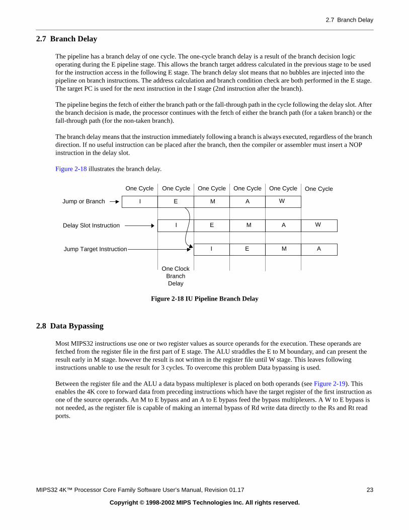
2.7 Branch Delay
ic be usedto the
stage.
After) or the
branchOP
s arent the
tion asypass isRt read
2.7 Branch Delay
The pipeline has a branch delay of one cycle. The one-cycle branch delay is a result of the branch decision logoperating during the E pipeline stage. This allows the branch target address calculated in the previous stage tofor the instruction access in the following E stage. The branch delay slot means that no bubbles are injected inpipeline on branch instructions. The address calculation and branch condition check are both performed in the EThe target PC is used for the next instruction in the I stage (2nd instruction after the branch).
The pipeline begins the fetch of either the branch path or the fall-through path in the cycle following the delay slot.the branch decision is made, the processor continues with the fetch of either the branch path (for a taken branchfall-through path (for the non-taken branch).
The branch delay means that the instruction immediately following a branch is always executed, regardless of thedirection. If no useful instruction can be placed after the branch, then the compiler or assembler must insert a Ninstruction in the delay slot.
Figure 2-18 illustrates the branch delay.
Figure 2-18 IU Pipeline Branch Delay
2.8 Data Bypassing
Most MIPS32 instructions use one or two register values as source operands for the execution. These operandfetched from the register file in the first part of E stage. The ALU straddles the E to M boundary, and can preseresult early in M stage. however the result is not written in the register file until W stage. This leaves followinginstructions unable to use the result for 3 cycles. To overcome this problem Data bypassing is used.
Between the register file and the ALU a data bypass multiplexer is placed on both operands (seeFigure 2-19). Thisenables the 4K core to forward data from preceding instructions which have the target register of the first instrucone of the source operands. An M to E bypass and an A to E bypass feed the bypass multiplexers. A W to E bnot needed, as the register file is capable of making an internal bypass of Rd write data directly to the Rs and ports.
One Cycle
Jump Target Instruction
Delay Slot Instruction
One ClockBranchDelay
One Cycle One Cycle One Cycle One Cycle One Cycle
I E M A W
I E M A W
I E M A
Jump or Branch
MIPS32 4K™ Processor Core Family Software User’s Manual, Revision 01.17 23
Copyright © 1998-2002 MIPS Technologies Inc. All rights reserved.
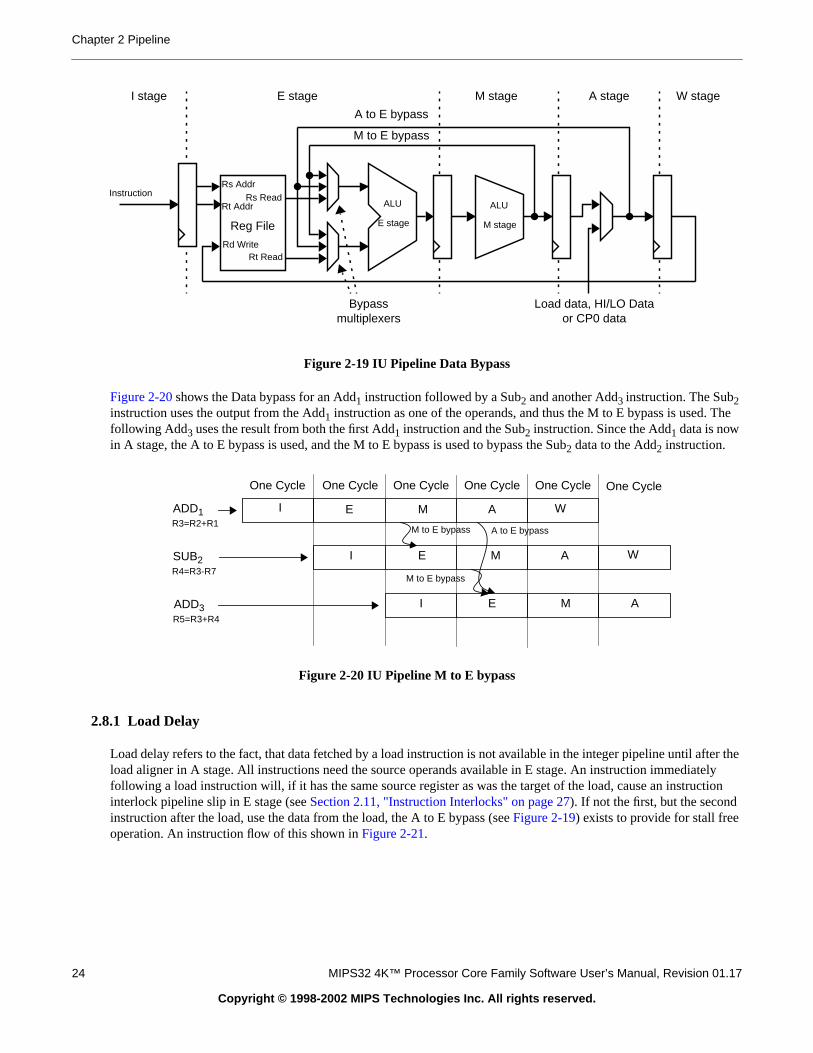
Chapter 2 Pipeline
The
ter theelyction
Figure 2-19 IU Pipeline Data Bypass
Figure 2-20shows the Data bypass for an Add1 instruction followed by a Sub2 and another Add3 instruction. The Sub2instruction uses the output from the Add1 instruction as one of the operands, and thus the M to E bypass is used. following Add3 uses the result from both the first Add1 instruction and the Sub2 instruction. Since the Add1 data is nowin A stage, the A to E bypass is used, and the M to E bypass is used to bypass the Sub2 data to the Add2 instruction.
Figure 2-20 IU Pipeline M to E bypass
2.8.1 Load Delay
Load delay refers to the fact, that data fetched by a load instruction is not available in the integer pipeline until afload aligner in A stage. All instructions need the source operands available in E stage. An instruction immediatfollowing a load instruction will, if it has the same source register as was the target of the load, cause an instruinterlock pipeline slip in E stage (seeSection 2.11, "Instruction Interlocks" on page 27). If not the first, but the secondinstruction after the load, use the data from the load, the A to E bypass (seeFigure 2-19) exists to provide for stall freeoperation. An instruction flow of this shown inFigure 2-21.
Bypassmultiplexers
E stage M stage A stage W stageI stage
Load data, HI/LO Dataor CP0 data
A to E bypass
M to E bypass
InstructionALU
M stage
ALU
E stageReg File
Rs Addr
Rt AddrRs Read
Rt ReadRd Write
One Cycle One Cycle One Cycle One Cycle One Cycle One Cycle
R3=R2+R1E M A W
I E M A W
I E M A
ADD1
R4=R3-R7
SUB2
R5=R3+R4
ADD3
I
A to E bypassM to E bypass
M to E bypass
24 MIPS32 4K™ Processor Core Family Software User’s Manual, Revision 01.17
Copyright © 1998-2002 MIPS Technologies Inc. All rights reserved.

2.9 Interlock Handling
heructionerlock
ptions
Figure 2-21 IU Pipeline A to E Data Bypass
2.8.2 Move from HI/LO and CP0 Delay
As indicated inFigure 2-19, not only load data, but also data from a move from the HI or LO register instruction(MFHI/MFLO) and a move from CP0 (MFC0) enter the IU-Pipeline in A stage. That is, data is not available in tinteger pipeline until early in the A stage. The A to E bypass is available for this data. But as for Loads the instimmediately after one of these instructions, can not use this data right away. If it does it will cause an instruction intslip in E stage (seeSection 2.11, "Instruction Interlocks" on page 27). An interlock slip after an MFHI is illustrated inFigure 2-22.
Figure 2-22 IU Pipeline Slip after MFHI
2.9 Interlock Handling
Smooth pipeline flow is interrupted when cache misses occur or when data dependencies are detected. Interruhandled using hardware, such as cache misses, are referred to asinterlocks. At each cycle, interlock conditions arechecked for all active instructions.
Table 2-4 lists the types of pipeline interlocks for the 4K processor cores.
Table 2-4 Pipeline Interlocks
Interlock Type Sources Slip Stage
ITLB Miss (4Kc core) Instruction TLB I Stage
ICache Miss Instruction cache E Stage
InstructionProducer-consumer hazards E/M Stage
Hardware Dependencies (MDU/TLB) E Stage
One Cycle One Cycle One Cycle One Cycle One Cycle One Cycle
I E M A W
I E M A W
I E M A
Load Instruction
Consumer of Load Data Instruction
Data bypass from A to E
One ClockLoad Delay
One Cycle One Cycle One Cycle One Cycle One Cycle One Cycle One Cycle
I E M A W
E M A WslipI
MFHI (to R3)
ADD (R4=R3+R5)
Data bypass from A to E
MIPS32 4K™ Processor Core Family Software User’s Manual, Revision 01.17 25
Copyright © 1998-2002 MIPS Technologies Inc. All rights reserved.
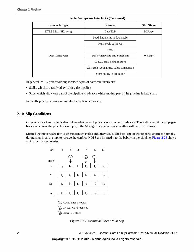
Chapter 2 Pipeline
opagate
ormally
In general, MIPS processors support two types of hardware interlocks:
• Stalls, which are resolved by halting the pipeline
• Slips, which allow one part of the pipeline to advance while another part of the pipeline is held static
In the 4K processor cores, all interlocks are handled as slips.
2.10 Slip Conditions
On every clock internal logic determines whether each pipe stage is allowed to advance. These slip conditions prbackwards down the pipe. For example, if the M stage does not advance, neither will the E or I stages.
Slipped instructions are retried on subsequent cycles until they issue. The back end of the pipeline advances nduring slips in an attempt to resolve the conflict. NOPS are inserted into the bubble in the pipeline.Figure 2-23 showsan instruction cache miss.
Figure 2-23 Instruction Cache Miss Slip
DTLB Miss (4Kc core) Data TLB M Stage
Data Cache Miss
Load that misses in data cache
W Stage
Multi-cycle cache Op
Sync
Store when write thru buffer full
EJTAG breakpoint on store
VA match needing data value comparison
Store hitting in fill buffer
Table 2-4 Pipeline Interlocks (Continued)
Interlock Type Sources Slip Stage
1 Cache miss detected
1 2
00
E
M I1 I2 I3
A
I
0I3I0 I1 I2
I4I4I2 I3 I4
I5I5I3 I4 I5
3 Execute E-stage
Stage
I4
0
I5
I6
3
Clock 1 2 3 4 5 6
2 Critical word received
26 MIPS32 4K™ Processor Core Family Software User’s Manual, Revision 01.17
Copyright © 1998-2002 MIPS Technologies Inc. All rights reserved.
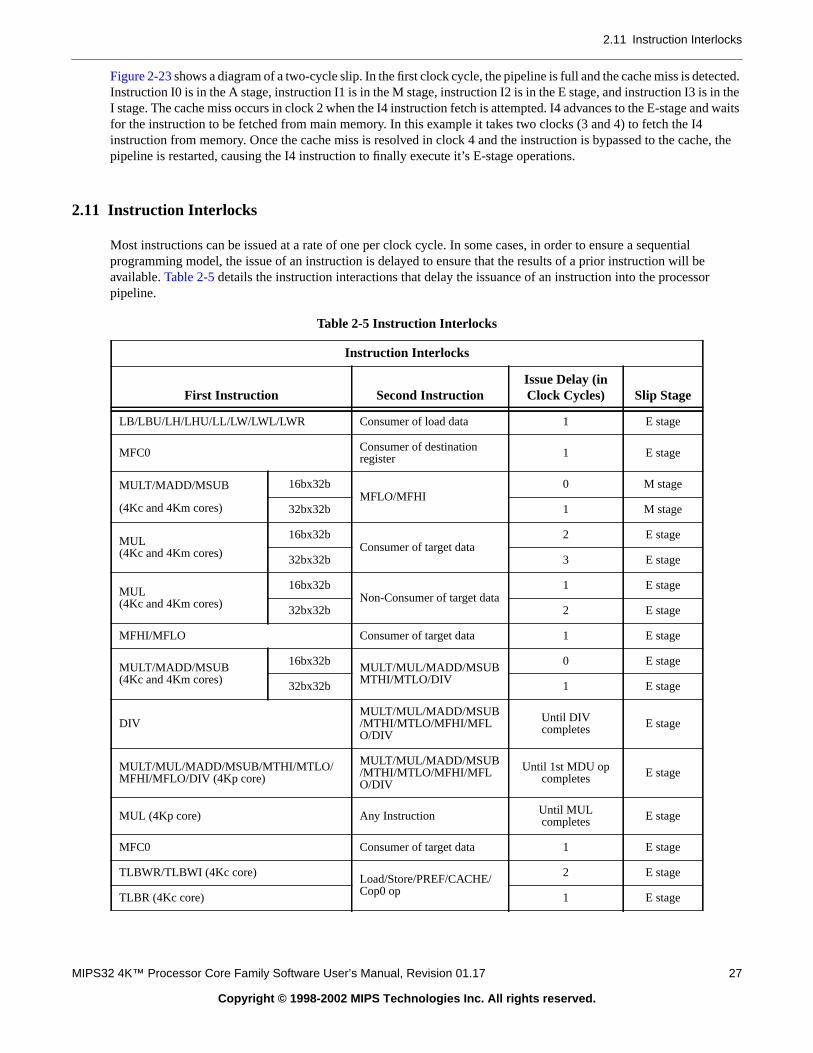
2.11 Instruction Interlocks
cted.n thend waits
he, the
l
r
Figure 2-23shows a diagram of a two-cycle slip. In the first clock cycle, the pipeline is full and the cache miss is deteInstruction I0 is in the A stage, instruction I1 is in the M stage, instruction I2 is in the E stage, and instruction I3 is iI stage. The cache miss occurs in clock 2 when the I4 instruction fetch is attempted. I4 advances to the E-stage afor the instruction to be fetched from main memory. In this example it takes two clocks (3 and 4) to fetch the I4instruction from memory. Once the cache miss is resolved in clock 4 and the instruction is bypassed to the cacpipeline is restarted, causing the I4 instruction to finally execute it’s E-stage operations.
2.11 Instruction Interlocks
Most instructions can be issued at a rate of one per clock cycle. In some cases, in order to ensure a sequentiaprogramming model, the issue of an instruction is delayed to ensure that the results of a prior instruction will beavailable.Table 2-5 details the instruction interactions that delay the issuance of an instruction into the processopipeline.
Table 2-5 Instruction Interlocks
Instruction Interlocks
First Instruction Second InstructionIssue Delay (inClock Cycles) Slip Stage
LB/LBU/LH/LHU/LL/LW/LWL/LWR Consumer of load data 1 E stage
MFC0 Consumer of destinationregister 1 E stage
MULT/MADD/MSUB
(4Kc and 4Km cores)
16bx32bMFLO/MFHI
0 M stage
32bx32b 1 M stage
MUL(4Kc and 4Km cores)
16bx32bConsumer of target data
2 E stage
32bx32b 3 E stage
MUL(4Kc and 4Km cores)
16bx32bNon-Consumer of target data
1 E stage
32bx32b 2 E stage
MFHI/MFLO Consumer of target data 1 E stage
MULT/MADD/MSUB(4Kc and 4Km cores)
16bx32b MULT/MUL/MADD/MSUBMTHI/MTLO/DIV
0 E stage
32bx32b 1 E stage
DIVMULT/MUL/MADD/MSUB/MTHI/MTLO/MFHI/MFLO/DIV
Until DIVcompletes E stage
MULT/MUL/MADD/MSUB/MTHI/MTLO/MFHI/MFLO/DIV (4Kp core)
MULT/MUL/MADD/MSUB/MTHI/MTLO/MFHI/MFLO/DIV
Until 1st MDU opcompletes E stage
MUL (4Kp core) Any Instruction Until MULcompletes E stage
MFC0 Consumer of target data 1 E stage
TLBWR/TLBWI (4Kc core) Load/Store/PREF/CACHE/Cop0 op
2 E stage
TLBR (4Kc core) 1 E stage
MIPS32 4K™ Processor Core Family Software User’s Manual, Revision 01.17 27
Copyright © 1998-2002 MIPS Technologies Inc. All rights reserved.
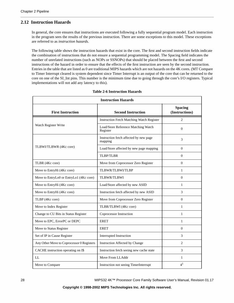
Chapter 2 Pipeline
ructionceptions
ndicates thend
uction.ompared to thepical
2.12 Instruction Hazards
In general, the core ensures that instructions are executed following a fully sequential program model. Each instin the program sees the results of the previous instruction. There are some exceptions to this model. These exare referred to asinstruction hazards.
The following table shows the instruction hazards that exist in the core. The first and second instruction fields ithe combination of instructions that do not ensure a sequential programming model. The Spacing field indicatenumber of unrelated instructions (such as NOPs or SSNOPs) that should be placed between the first and secoinstructions of the hazard in order to ensure that the effects of the first instruction are seen by the second instrEntries in the table that are listed as 0 are traditional MIPS hazards which are not hazards on the 4K cores. (MT Cto Timer Interrupt cleared is system dependent since Timer Interrupt is an output of the core that can be returnecore on one of the SI_Int pins. This number is the minimum time due to going through the core’s I/O registers. Tyimplementations will not add any latency to this).
Table 2-6 Instruction Hazards
Instruction Hazards
First Instruction Second InstructionSpacing
(Instructions)
Watch Register Write
Instruction Fetch Matching Watch Register 2
Load/Store Reference Matching WatchRegister 0
TLBWI/TLBWR (4Kc core)
Instruction fetch affected by new pagemapping 3
Load/Store affected by new page mapping 0
TLBP/TLBR 0
TLBR (4Kc core) Move from Coprocessor Zero Register 0
Move to EntryHi (4Kc core) TLBWR/TLBWI/TLBP 1
Move to EntryLo0 or EntryLo1 (4Kc core) TLBWR/TLBWI 0
Move to EntryHi (4Kc core) Load/Store affected by new ASID 1
Move to EntryHi (4Kc core) Instruction fetch affected by new ASID 3
TLBP (4Kc core) Move from Coprocessor Zero Register 0
Move to Index Register TLBR/TLBWI (4Kc core) 1
Change to CU Bits in Status Register Coprocessor Instruction 1
Move to EPC, ErrorPC or DEPC ERET 1
Move to Status Register ERET 0
Set of IP in Cause Register Interrupted Instruction 3
Any Other Move to Coprocessor 0 Registers Instruction Affected by Change 2
CACHE instruction operating on I$ Instruction fetch seeing new cache state 3
LL Move From LLAddr 1
Move to Compare Instruction not seeing TimerInterrupt 41
28 MIPS32 4K™ Processor Core Family Software User’s Manual, Revision 01.17
Copyright © 1998-2002 MIPS Technologies Inc. All rights reserved.
2.12 Instruction Hazards
1. This is the minimum value. Actual value is system-dependent since it is a function of the sequential logic between the SI_TimerInt outputand the external logic which feeds SI_TimerInt back into one of the SI_Int inputs.
MIPS32 4K™ Processor Core Family Software User’s Manual, Revision 01.17 29
Copyright © 1998-2002 MIPS Technologies Inc. All rights reserved.
Chapter 2 Pipeline
30 MIPS32 4K™ Processor Core Family Software User’s Manual, Revision 01.17
Copyright © 1998-2002 MIPS Technologies Inc. All rights reserved.
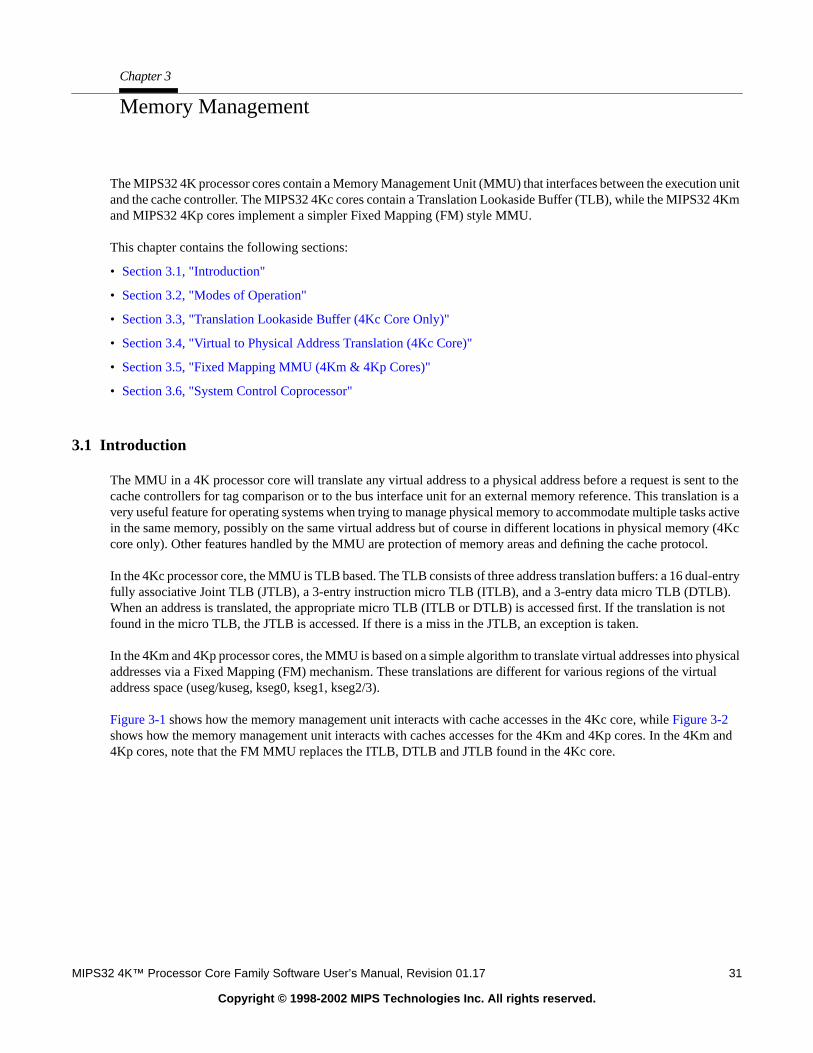
on unit4Km
nt to theion is as activey (4Kcl.
l-entry). not
hysicaltual
Km and
Chapter 3
Memory Management
The MIPS32 4K processor cores contain a Memory Management Unit (MMU) that interfaces between the executiand the cache controller. The MIPS32 4Kc cores contain a Translation Lookaside Buffer (TLB), while the MIPS32and MIPS32 4Kp cores implement a simpler Fixed Mapping (FM) style MMU.
This chapter contains the following sections:
• Section 3.1, "Introduction"
• Section 3.2, "Modes of Operation"
• Section 3.3, "Translation Lookaside Buffer (4Kc Core Only)"
• Section 3.4, "Virtual to Physical Address Translation (4Kc Core)"
• Section 3.5, "Fixed Mapping MMU (4Km & 4Kp Cores)"
• Section 3.6, "System Control Coprocessor"
3.1 Introduction
The MMU in a 4K processor core will translate any virtual address to a physical address before a request is secache controllers for tag comparison or to the bus interface unit for an external memory reference. This translatvery useful feature for operating systems when trying to manage physical memory to accommodate multiple taskin the same memory, possibly on the same virtual address but of course in different locations in physical memorcore only). Other features handled by the MMU are protection of memory areas and defining the cache protoco
In the 4Kc processor core, the MMU is TLB based. The TLB consists of three address translation buffers: a 16 duafully associative Joint TLB (JTLB), a 3-entry instruction micro TLB (ITLB), and a 3-entry data micro TLB (DTLBWhen an address is translated, the appropriate micro TLB (ITLB or DTLB) is accessed first. If the translation isfound in the micro TLB, the JTLB is accessed. If there is a miss in the JTLB, an exception is taken.
In the 4Km and 4Kp processor cores, the MMU is based on a simple algorithm to translate virtual addresses into paddresses via a Fixed Mapping (FM) mechanism. These translations are different for various regions of the viraddress space (useg/kuseg, kseg0, kseg1, kseg2/3).
Figure 3-1 shows how the memory management unit interacts with cache accesses in the 4Kc core, whileFigure 3-2shows how the memory management unit interacts with caches accesses for the 4Km and 4Kp cores. In the 44Kp cores, note that the FM MMU replaces the ITLB, DTLB and JTLB found in the 4Kc core.
MIPS32 4K™ Processor Core Family Software User’s Manual, Revision 01.17 31
Copyright © 1998-2002 MIPS Technologies Inc. All rights reserved.
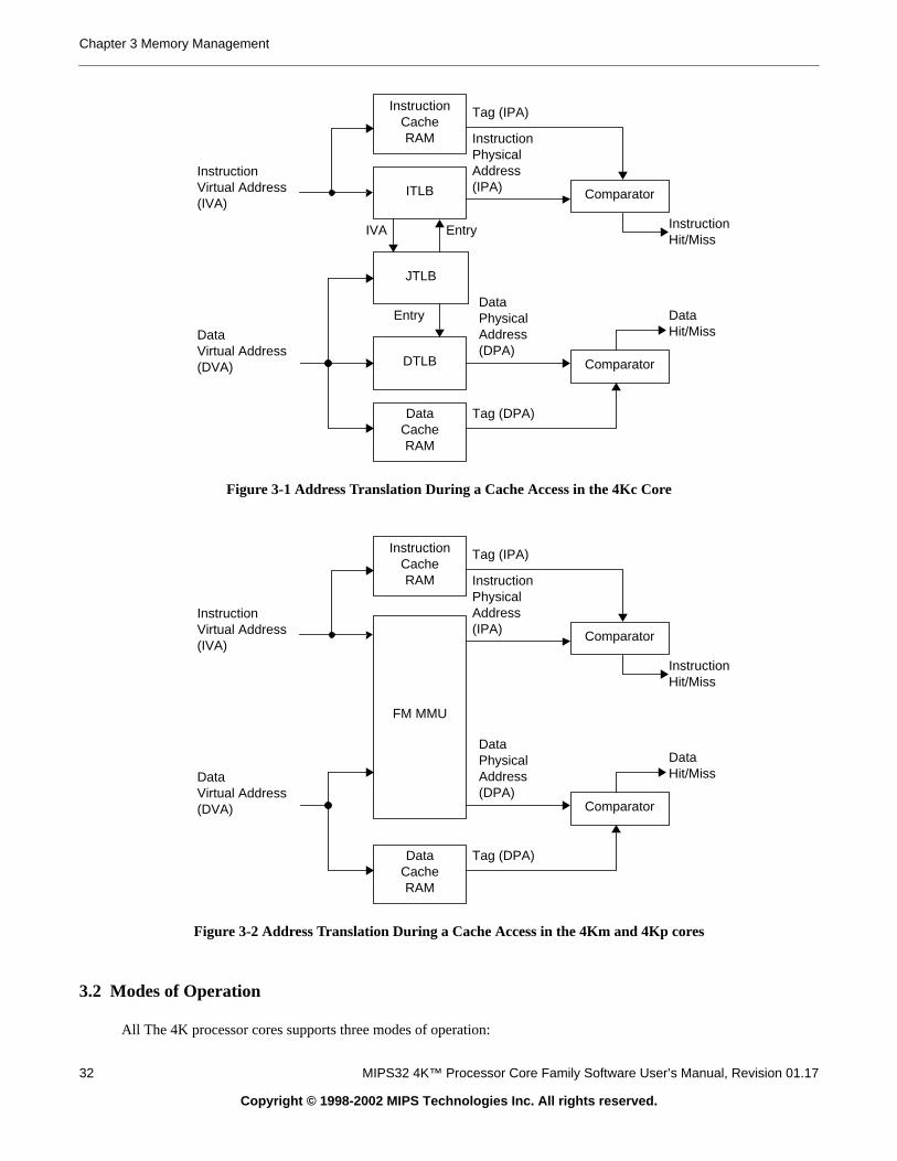
Chapter 3 Memory Management
Figure 3-1 Address Translation During a Cache Access in the 4Kc Core
Figure 3-2 Address Translation During a Cache Access in the 4Km and 4Kp cores
3.2 Modes of Operation
All The 4K processor cores supports three modes of operation:
InstructionVirtual Address(IVA)
DataVirtual Address(DVA)
JTLB
ITLB
InstructionCacheRAM
DTLB
DataCacheRAM
IVA Entry
EntryDataPhysicalAddress(DPA)
InstructionPhysicalAddress(IPA)
Tag (IPA)
Tag (DPA)
Comparator
Comparator
DataHit/Miss
InstructionHit/Miss
InstructionVirtual Address(IVA)
DataVirtual Address(DVA)
FM MMU
InstructionCacheRAM
DataCacheRAM
DataPhysicalAddress(DPA)
InstructionPhysicalAddress(IPA)
Tag (IPA)
Tag (DPA)
Comparator
Comparator
DataHit/Miss
InstructionHit/Miss
32 MIPS32 4K™ Processor Core Family Software User’s Manual, Revision 01.17
Copyright © 1998-2002 MIPS Technologies Inc. All rights reserved.

3.2 Modes of Operation
andsed for
ration.
re hasthe virtualode,
e addresssegmentallowing
• User mode
• Kernel mode
• Debug mode
User mode is most often used for application programs. Kernel mode is typically used for handling exceptions privileged operating system functions, including CP0 management and I/O device accesses. Debug mode is usoftware debugging and most likely occurs within a software development tool.
The address translation performed by the MMU depends on the mode in which the processor is operating.
3.2.1 Virtual Memory Segments
The Virtual memory segments are different depending on the mode of operation.Figure 3-3shows the segmentation forthe 4 GByte (232 bytes) virtual memory space addressed by a 32-bit virtual address, for the three modes of ope
The core enters Kernel mode both at reset and when an exception is recognized. While in Kernel mode, softwaaccess to the entire address space, as well as all CP0 registers. User mode accesses are limited to a subset ofaddress space (0x0000_0000 to 0x7FFF_FFFF) and can be inhibited from accessing CP0 functions. In User mvirtual addresses 0x8000_0000 to 0xFFFF_FFFF are invalid and cause an exception if accessed.
Debug mode is entered on a debug exception. While in Debug mode, the debug software has access to the samspace and CP0 registers as for Kernel mode. In addition, while in Debug mode the core has access to the debugdseg. This area overlays part of the kernel segment kseg3. dseg access in Debug mode can be turned on or off,full access to the entire kseg3 in Debug mode, if so desired.
MIPS32 4K™ Processor Core Family Software User’s Manual, Revision 01.17 33
Copyright © 1998-2002 MIPS Technologies Inc. All rights reserved.

Chapter 3 Memory Management
he
al tonot yet
lations
he CP0
Figure 3-3 4K Processor Core Virtual Memory Map
Each of the segments shown inFigure 3-3 is either mapped or unmapped. The following two subsections explain tdistinction. ThenSection 3.2.2, "User Mode", Section 3.2.3, "Kernel Mode"andSection 3.2.4, "Debug Mode"specifywhich segments are actually mapped and unmapped.
3.2.1.1 Unmapped Segments
An unmapped segment does not use the TLB (4Kc core) or the FM (4Km and 4Kp cores) to translate from virtuphysical address. Especially after reset it is important to have unmapped memory segments, because the TLB isprogrammed to perform the translation.
Unmapped segments have a fixed simple translation from virtual to physical address. This is much like the transthe FM provides for the 4Km and 4Kp cores, but we will still make the distinction.
Except for kseg0, unmapped segments are always uncached. The cacheability of kseg0 is set in the K0 field of tregisterConfig (seeSection 5.2.15, "Config Register (CP0 Register 16, Select 0)").
useg kuseg kuseg
kseg0
kseg1
kseg2
kseg3
kseg2
kseg1
kseg0
kseg3
kseg3
dseg
User Mode Kernel Mode Debug ModeVirtual Address
0x7FFF_FFFF
0x8000_0000
0x9FFF_FFFF
0xBFFF_FFFF
0xDFFF_FFFF
0xF1FF_FFFF
0xF3FF_FFFF
0xFFFF_FFFF
0xA000_0000
0xC000_0000
0xE000_0000
0xF200_0000
0xF400_0000
0x0000_0000
34 MIPS32 4K™ Processor Core Family Software User’s Manual, Revision 01.17
Copyright © 1998-2002 MIPS Technologies Inc. All rights reserved.
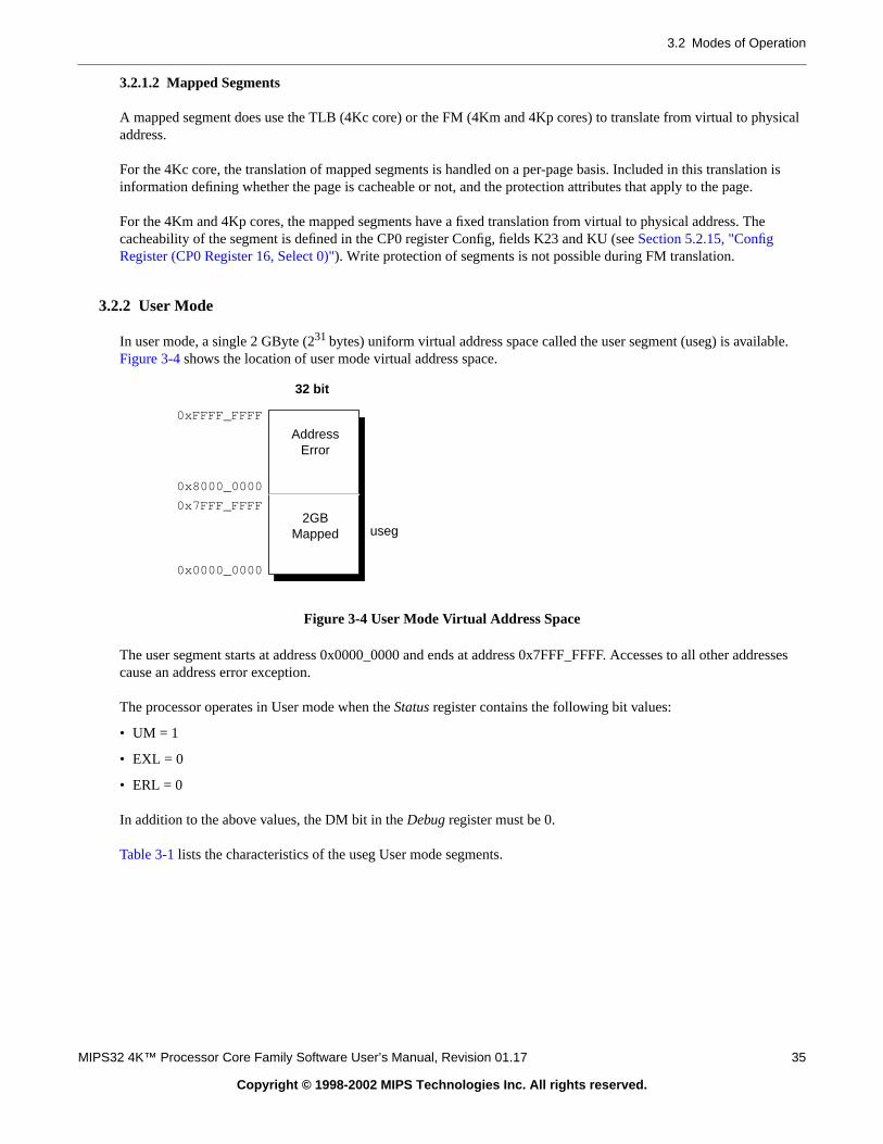
3.2 Modes of Operation
ysical
ion is
e
le.
ddresses
3.2.1.2 Mapped Segments
A mapped segment does use the TLB (4Kc core) or the FM (4Km and 4Kp cores) to translate from virtual to phaddress.
For the 4Kc core, the translation of mapped segments is handled on a per-page basis. Included in this translatinformation defining whether the page is cacheable or not, and the protection attributes that apply to the page.
For the 4Km and 4Kp cores, the mapped segments have a fixed translation from virtual to physical address. Thcacheability of the segment is defined in the CP0 register Config, fields K23 and KU (seeSection 5.2.15, "ConfigRegister (CP0 Register 16, Select 0)"). Write protection of segments is not possible during FM translation.
3.2.2 User Mode
In user mode, a single 2 GByte (231bytes) uniform virtual address space called the user segment (useg) is availabFigure 3-4 shows the location of user mode virtual address space.
Figure 3-4 User Mode Virtual Address Space
The user segment starts at address 0x0000_0000 and ends at address 0x7FFF_FFFF. Accesses to all other acause an address error exception.
The processor operates in User mode when theStatus register contains the following bit values:
• UM = 1
• EXL = 0
• ERL = 0
In addition to the above values, the DM bit in theDebug register must be 0.
Table 3-1 lists the characteristics of the useg User mode segments.
0x0000_0000
0x8000_0000
0x7FFF_FFFF
0xFFFF_FFFF
32 bit
AddressError
2GBMapped useg
MIPS32 4K™ Processor Core Family Software User’s Manual, Revision 01.17 35
Copyright © 1998-2002 MIPS Technologies Inc. All rights reserved.

Chapter 3 Memory Management
onlyt bit set
e
and
e enduction.
ss, as
All valid user mode virtual addresses have their most-significant bit cleared to 0, indicating that user mode canaccess the lower half of the virtual memory map. Any attempt to reference an address with the most-significanwhile in user mode causes an address error exception.
The system maps all references tousegthrough the TLB (4Kc core) or FM (4Km and 4Kp cores). For the 4Kc core, thThe virtual address is extended with the contents of the 8-bit ASID field to form a unique virtual address beforetranslation. Bit settings within the TLB entry for the page determine the cacheability of a reference. For the 4Km4Kp cores, the cacheability is set via the KU field of the CP0Config register.
3.2.3 Kernel Mode
The processor operates in Kernel mode when the DM bit in theDebugregister is 0 and theStatusregister contains oneor more of the following values:
• UM = 0
• ERL = 1
• EXL = 1
When a non-debug exception is detected, EXL or ERL will be set and the processor will enter Kernel mode. At thof the exception handler routine, an Exception Return (ERET) instruction is generally executed. The ERET instrjumps to the Exception PC, clears ERL, and clears EXL if ERL=0. This may return the processor to User mode
Kernel mode virtual address space is divided into regions differentiated by the high-order bits of the virtual addreshown inFigure 3-5. Also,Table 3-2 lists the characteristics of the Kernel mode segments.
Table 3-1 User Mode Segments
AddressBit Value
Status Register
Segment
Name Address Range Segment Size
Bit Value
EXL ERL UM
32-bit
A(31) = 00 0 1 useg
0x0000_0000 -->
0x7FFF_FFFF
2 GByte(231 bytes)
36 MIPS32 4K™ Processor Core Family Software User’s Manual, Revision 01.17
Copyright © 1998-2002 MIPS Technologies Inc. All rights reserved.

3.2 Modes of Operation
Figure 3-5 Kernel Mode Virtual Address Space
Table 3-2 Kernel Mode Segments
Address BitValues
Status Register IsOne of These Values
SegmentName Address Range
SegmentSizeUM EXL ERL
A(31) = 0
(UM = 0
or
EXL = 1
or
ERL = 1)
and
DM = 0
kuseg0x0000_0000
through0x7FFF_FFFF
2 GBytes(231 bytes)
A(31:29) = 1002 kseg00x8000_0000
through0x9FFF_FFFF
512 MBytes(229 bytes)
A(31:29) = 1012 kseg10xA000_0000
through0xBFFF_FFFF
512 MBytes(229 bytes)
A(31:29) = 1102 kseg20xC000_0000
through0xDFFF_FFFF
512 MBytes(229 bytes)
A(31:29) = 1112 kseg30xE000_0000
through0xFFFF_FFFF
512 MBytes(229 bytes)
Kernel virtual address spaceUnmapped, 512MB
kuseg
kseg0
kseg1
kseg2
kseg3
Mapped, 2048MB
Kernel virtual address spaceUnmapped, Uncached, 512MB
Kernel virtual address spaceMapped, 512MB
Kernel virtual address spaceMapped, 512MB
0x0000_0000
0x8000_0000
0xA000_0000
0xC000_0000
0xE000_0000
0x7FFF_FFFF
0x9FFF_FFFF
0xBFFF_FFFF
0xDFFF_FFFF
0xFFFF_FFFF
MIPS32 4K™ Processor Core Family Software User’s Manual, Revision 01.17 37
Copyright © 1998-2002 MIPS Technologies Inc. All rights reserved.
Chapter 3 Memory Management
dress
D field
ce.e ASID
F.he virtual
mory (or
e 4Km
-or core.
areas,F_FFFF.
3.2.3.1 Kernel Mode, User Space (kuseg)
In Kernel mode, when the most-significant bit of the virtual address (A31) is cleared, the 32-bit kuseg virtual adspace is selected and covers the full 231bytes (2 GByte) of the current user address space mapped to addresses0x0000_0000 - 0x7FFF_FFFF. For the 4Kc core, the virtual address is extended with the contents of the 8-bit ASIto form a unique virtual address.
When ERL = 1 in theStatusregister, the user address region becomes a 231-byte unmapped and uncached address spaWhile in this setting, the kuseg virtual address maps directly to the same physical address, and does not include thfield.
3.2.3.2 Kernel Mode, Kernel Space 0 (kseg0)
In Kernel mode, when the most-significant three bits of the virtual address are 1002, 32-bit kseg0 virtual address spaceis selected; it is the 229-byte (512-MByte) kernel virtual space located at addresses 0x8000_0000 - 0x9FFF_FFFReferences to kseg0 are unmapped; the physical address selected is defined by subtracting 0x8000_0000 from taddress. The K0 field of theConfig register controls cacheability.
3.2.3.3 Kernel Mode, Kernel Space 1 (kseg1)
In Kernel mode, when the most-significant three bits of the 32-bit virtual address are 1012, 32-bit kseg1 virtual addressspace is selected. kseg1 is the 229-byte (512-MByte) kernel virtual space located at addresses 0xA000_0000 -0xBFFF_FFFF. References to kseg1 are unmapped; the physical address selected is defined by subtracting0xA000_0000 from the virtual address. Caches are disabled for accesses to these addresses, and physical mememory-mapped I/O device registers) are accessed directly.
3.2.3.4 Kernel Mode, Kernel Space 2 (kseg2)
In Kernel mode, when UM = 0, ERL = 1, or EXL = 1 in theStatus register, and DM = 0 in theDebug register, and themost-significant three bits of the 32-bit virtual address are 1102, 32-bit kseg2 virtual address space is selected. This229-byte (512-MByte) kernel virtual space is located at physical addresses 0xC000_0000 - 0xDFFF_FFFF in thand 4Kp processor cores. This space is mapped through the TLB in the 4Kc processor core.
3.2.3.5 Kernel Mode, Kernel Space 3 (kseg3)
In Kernel mode, when the most-significant three bits of the 32-bit virtual address are 1112, the kseg3 virtual addressspace is selected. This 229-byte (512-MByte) kernel virtual space is located at physical addresses 0xE000_0000 0xFFFF_FFFF in the 4Km and 4Kp processor cores. This space is mapped through the TLB in the 4Kc process
3.2.4 Debug Mode
Debug mode address space is identical to Kernel mode address space with respect to mapped and unmappedexcept for kseg3. In kseg3, a debug segment dseg co-exists in the virtual address range 0xFF20_0000 to 0xFF3The layout is shown inFigure 3-6.
38 MIPS32 4K™ Processor Core Family Software User’s Manual, Revision 01.17
Copyright © 1998-2002 MIPS Technologies Inc. All rights reserved.

3.2 Modes of Operation
obe memory
r debugith the
ich allows
hown in
Figure 3-6 Debug Mode Virtual Address Space
The dseg is sub-divided into the dmseg segment at 0xFF20_0000 to 0xFF2F_FFFF which is used when the prservices the memory segment, and the drseg segment at 0xFF30_0000 to 0xFF3F_FFFF which is used whenmapped debug registers are accessed. The subdivision and attributes for the segments are shown inTable 3-3.
Accesses to memory that would normally cause an exception if tried from kernel mode cause the core to re-entemode via a debug mode exception. This includes accesses usually causing a TLB exception (4Kc core only), wresult that such accesses are not handled by the usual memory management routines.
The unmapped kseg0 and kseg1 segments from kernel mode address space are available from debug mode, whthe debug handler to be executed from uncached and unmapped memory.
3.2.4.1 Conditions and Behavior for Access to drseg, EJTAG Registers
The behavior of CPU access to the drseg address range at 0xFF30_0000 to 0xFF3F_FFFF is determined as sTable 3-4.
Table 3-3 Physical Address and Cache Attributes for dseg, dmseg, and drseg Address Spaces
SegmentName
Sub-SegmentName Virtual Address Generates Physical Address
CacheAttribute
dseg
dmseg
0xFF20_0000
through
0xFF2F_FFFF
dmseg maps to addresses0x0_0000 - 0xF_FFFF in EJTAG
probe memory space.
drseg maps to the breakpointregisters 0x0_0000 - 0xF_FFFF
Uncached
drseg
0xFF30_0000
through
0xFF3F_FFFF
Table 3-4 CPU Access to drseg Address Range
TransactionLSNM bit in Debug
register Access
Load / Store 1 Kernel mode address space (kseg3)
Fetch Don’t caredrseg, see comments below
Load / Store 0
0x0000_0000
0xFF20_0000
0xFF40_00000xFFFF_FFFF
dseg
kseg1
kseg0 Unmapped
Mapped if mapped in Kernel Mode
MIPS32 4K™ Processor Core Family Software User’s Manual, Revision 01.17 39
Copyright © 1998-2002 MIPS Technologies Inc. All rights reserved.

Chapter 3 Memory Management
egistersdictable,
ssor is
ebugIf such there willeen the
TLB
ndingize fromresses
formed
referred
tag
Debug software is expected to read the debug control register (DCR) to determine which other memory mapped rexist in drseg. The value returned in response to a read of any unimplemented memory mapped register is unpreand writes are ignored to any unimplemented register in the drseg. Refer toChapter 9, “EJTAG Debug Support,” on page121 for more information on the DCR.
The allowed access size is limited for the drseg. Only word size transactions are allowed. Operation of the proceundefined for other transaction sizes.
3.2.4.2 Conditions and Behavior for Access to dmseg, EJTAG Memory
The behavior of CPU access to the dmseg address range at 0xFF20_0000 to 0xFF2F_FFFF is determined byTable 3-5..
The case with access to the dmseg when the ProbEn bit in the DCR register is 0 is not expected to happen. Dsoftware is expected to check the state of the ProbEn bit in DCR register before attempting to reference dmseg.a reference does happen, the reference hangs until it is satisfied by the probe. The probe can not assume thatnever be a reference to dmseg if the ProbEn bit in the DCR register is 0 because there is an inherent race betwdebug software sampling the ProbEn bit as 1 and the probe clearing it to 0.
3.3 Translation Lookaside Buffer (4Kc Core Only)
The following subsections discuss the TLB memory management scheme used in the 4Kc processor core. Theconsists of one joint and two micro address translation buffers:
• 16 dual-entry fully associative Joint TLB (JTLB)
• 3-entry fully associative Instruction micro TLB (ITLB)
• 3-entry fully associative Data micro TLB (DTLB)
3.3.1 Joint TLB
The 4Kc core implements a 16 dual-entry, fully associative Joint TLB that maps 32 virtual pages to their correspophysical addresses. The JTLB is organized as 16 pairs of even and odd entries containing pages that range in s4-KBytes to 16-MBytes into the 4-GByte physical address space. The purpose of the TLB is to translate virtual addand their corresponding Address Space Identifier (ASID) into a physical memory address. The translation is perby comparing the upper bits of the virtual address (along with the ASID bits) against each of the entries in thetagportionof the JTLB structure. Because this structure is used to translate both instruction and data virtual addresses, it isto as a “joint” TLB.
The JTLB is organized in page pairs to minimize its overall size. Each virtualtagentry corresponds to two physical dataentries, an even page entry and an odd page entry. The highest order virtual address bit not participating in the
Table 3-5 CPU Access to dmseg Address Range
TransactionProbEn bit inDCR register
LSNM bit inDebug register Access
Load / Store Don’t care 1 Kernel mode address space (kseg3)
Fetch 1 Don’t caredmseg
Load / Store 1 0
Fetch 0 Don’t careSee comments below
Load / Store 0 0
40 MIPS32 4K™ Processor Core Family Software User’s Manual, Revision 01.17
Copyright © 1998-2002 MIPS Technologies Inc. All rights reserved.

3.3 Translation Lookaside Buffer (4Kc Core Only)
asis, the
comparison is used to determine which of the two data entries is used. Since page size can vary on a page-pair bdetermination of which address bits participate in the comparison and which bit is used to make the even-odddetermination must be determined dynamically during the TLB lookup.Figure 3-7 show the contents of one of the 16 dual-entries in the JTLB.
Figure 3-7 JTLB Entry (Tag and Data)
Table 3-6 andTable 3-7 explain each of the fields in a JTLB entry.
Table 3-6 TLB Tag Entry Fields
Field Name Description
PageMask[24:13]
Page Mask Value. The Page Mask defines the page size by masking theappropriate VPN2 bits from being involved in a comparison. It is also used todetermine which address bit is used to make the even-odd page (PFN0-PFN1)determination. See the table below.
The PageMask column above show all the legal values for PageMask. Becauseeach pair of bits can only have the same value, the physical entry in the JTLBwill only save a compressed version of the PageMask using only 6 bits. This ishowever transparent to software, which will always work with a 12 bit field.
VPN2[31:13]
Virtual Page Number divided by 2. This field contains the upper bits of thevirtual page number. Because it represents a pair of TLB pages, it is divided by2. Bits 31:25 are always included in the TLB lookup comparison. Bits 24:13are included depending on the page size, defined by PageMask.
G Global Bit. When set, indicates that this entry is global to all processes and/orthreads and thus disables inclusion of the ASID in the comparison.
ASID[7:0] Address Space Identifier. Identifies which process or thread this TLB entry isassociated with.
PageMask[24:13]
D0
G ASID[7:0]
PFN0[31:12] C0[2:0]
D1PFN1[31:12] C1[2:0]
VPN2[31:13]
V0
V1
GTag Entry
Data Entries
19 1 8
20 3 1 1
PageMask[11:0] Page Size Even/Odd BankSelect Bit
0000_0000_0000 4KB VAddr[12]
0000_0000_0011 16KB VAddr[14]
0000_0000_1111 64KB VAddr[16]
0000_0011_1111 256KB VAddr[18]
0000_1111_1111 1MB VAddr[20]
0011_1111_1111 4MB VAddr[22]
1111_1111_1111 16MB VAddr[24]
MIPS32 4K™ Processor Core Family Software User’s Manual, Revision 01.17 41
Copyright © 1998-2002 MIPS Technologies Inc. All rights reserved.

Chapter 3 Memory Management
the
istencein the
. The
In order to fill an entry in the JTLB, software executes a TLBWI or TLBWR instruction (SeeSection 3.4.3, "TLBInstructions" on page 47). Prior to invoking one of these instructions, several CP0 registers must be updated withinformation to be written to a TLB entry.
• PageMask is set in the CP0PageMask register.
• VPN2 and ASID are set in the CP0EntryHi register.
• PFN0, C0, D0, V0 and G bit are set in the CP0EntryLo0 register.
• PFN1, C1, D1, V1 and G bit are set in the CP0EntryLo1 register.
Note that the global bit “G” is part of bothEntryLo0andEntryLo1. The resulting “G” bit in the JTLB entry is the logicalAND between the two fields inEntryLo0 andEntryLo1. Please refer toChapter 5, “CP0 Registers,” on page 73 forfurther details.
The address space identifier (ASID) helps to reduce the frequency of TLB flushing on a context switch. The exof the ASID allows multiple processes to exist in both the TLB and instruction caches. The ASID value is storedEntryHi register and is compared to the ASID value of each entry.
3.3.2 Instruction TLB
The ITLB is a small 3-entry, fully associative TLB dedicated to performing translations for the instruction streamITLB only maps 4-Kbyte pages/sub-pages.
Table 3-7 TLB Data Entry Fields
Field Name Description
PFN0[31:12],PFN1[31:12]
Physical Frame Number. Defines the upper bits of the physical address.For page sizes larger than 4 KBytes, only a subset of these bits is actuallyused.
C0[2:0],C1[2:0]
Cacheability. Contains an encoded value of the cacheability attributes anddetermines whether the page should be placed in the cache or not. The fieldis encoded as follows:
D0,D1
“Dirty” or Write-enable Bit. Indicates that the page has been written,and/or is writable. If this bit is set, stores to the page are permitted. If thebit is cleared, stores to the page cause a TLB Modified exception.
V0,V1
Valid Bit. Indicates that the TLB entry and, thus, the virtual page mappingare valid. If this bit is set, accesses to the page are permitted. If the bit iscleared, accesses to the page cause a TLB Invalid exception.
C[2:0] Coherency Attribute
000 Maps to entry 011b*
001 Maps to entry 011b*
010 Uncached
011Cacheable, noncoherent, write-through,no write allocated
100 Maps to entry 011b*
101 Maps to entry 011b*
110 Maps to entry 011b*
111 Maps to entry 010b*
Note: * These mappings are not used on the 4K proces-sor cores but do have meaning in other MIPS
42 MIPS32 4K™ Processor Core Family Software User’s Manual, Revision 01.17
Copyright © 1998-2002 MIPS Technologies Inc. All rights reserved.

3.4 Virtual to Physical Address Translation (4Kc Core)
e ITLB,tion iss in an
han is
tingDTLBaccess
with the as the
re
uencyred in
The ITLB is managed by hardware and is transparent to software. If a fetch address cannot be translated by ththe JTLB is accessed to attempt to translate it in the following clock cycle. If successful, the translation informacopied into the ITLB. The ITLB is then re-accessed and the address will be successfully translated. This resultITLB miss penalty of at least 2 cycles (if the JTLB is busy with other operations, it may take additional cycles).
3.3.3 Data TLB
The DTLB is a small 3-entry, fully associative TLB which provides a faster translation for Load/Store addresses tpossible with the JTLB. The DTLB only maps 4-Kbyte pages/sub-pages.
Like the ITLB, the DTLB is managed by hardware and is transparent to software. Unlike the ITLB, when translaLoad/Store addresses, the JTLB is accessed in parallel with the DTLB. If there is a DTLB miss and a JTLB hit, thecan be reloaded that cycle. The DTLB is then re-accessed and the translation will be successful. This parallel reduces the DTLB miss penalty to 1 cycle.
3.4 Virtual to Physical Address Translation (4Kc Core)
Converting a virtual address to a physical address begins by comparing the virtual address from the processorvirtual addresses in the TLB. There is a match when the virtual page number (VPN) of the address is the sameVPN field of the entry, and either:
• The Global (G) bit of both the even and odd pages of the TLB entry are set, or
• The ASID field of the virtual address is the same as the ASID field of the TLB entry
This match is referred to as a TLBhit. If there is no match, a TLBmissexception is taken by the processor and softwais allowed to refill the TLB from a page table of virtual/physical addresses in memory.
Figure 3-8 shows the logical translation of a virtual address into a physical address.
In this figure the virtual address is extended with an 8-bit address-space identifier (ASID), which reduces the freqof TLB flushing during a context switch. This 8-bit ASID contains the number assigned to that process and is stothe CP0EntryHi register.
MIPS32 4K™ Processor Core Family Software User’s Manual, Revision 01.17 43
Copyright © 1998-2002 MIPS Technologies Inc. All rights reserved.

Chapter 3 Memory Management
natedn in
virtualess
ress
Figure 3-8 Overview of a Virtual-to-Physical Address Translation in the 4Kc Core
If there is a virtual address match in the TLB, the physical frame number (PFN) is output from the TLB and concatewith theOffset, to form the physical address. TheOffsetrepresents an address within the page frame space. As showFigure 3-8, theOffset does not pass through the TLB.
Figure 3-9shows a flow diagram of the 4Kc core address translation process. The top portion of the figure shows aaddress for a 4-KByte page size. The width of theOffsetis defined by the page size. The remaining 20 bits of the addrrepresent the virtual page number (VPN), that index the 1M-entry page table.
The bottom portion ofFigure 3-9shows the virtual address for a 16-MByte page size. The remaining 8 bits of the addrepresent the VPN, that index the 256-entry page table.
1.Virtual address (VA) represented bythe virtual page number (VPN) iscompared with tag in TLB.
2. If there is a match, the page framenumber (PFN0 or PFN1)representing the upper bits of thephysical address (PA) is output fromthe TLB.
3. The Offset, which does not passthrough the TLB, is then concatenatedwith the PFN.
OffsetVPNG ASID
Virtual Address
TLBEntry
OffsetPFN
TLB
G ASID VPN2
C0 D0 V0 PFN0
PFN1C1 D1 V1
Physical Address
44 MIPS32 4K™ Processor Core Family Software User’s Manual, Revision 01.17
Copyright © 1998-2002 MIPS Technologies Inc. All rights reserved.

3.4 Virtual to Physical Address Translation (4Kc Core)
placedarity of fromTLB
in
the
n, the
n the, ther
on.
thewith
Figure 3-9 32-bit Virtual Address Translation
3.4.1 Hits, Misses, and Multiple Matches
Each JTLB entry contains a tag and two data fields. If a match is found, the upper bits of the virtual address are rewith the page frame number (PFN) stored in the corresponding entry in the data array of the JTLB. The granulJTLB mappings is defined in terms of TLB pages. The 4Kc core JTLB supports pages of different sizes ranging4-KB to 16-MB in powers of 4. If a match is found, but the entry is invalid (i.e., the V bit in the data field is 0), a Invalid exception is taken.
If no match occurs (TLB miss), an exception is taken and software refills the TLB from the page table resident memory.Figure 3-10 show the translation and exception flow of the TLB.
Software can write over a selected TLB entry or use a hardware mechanism to write into a random entry. TheRandomregister selects which TLB entry to use on a TLBWR. This register decrements almost every cycle, wrapping tomaximum once it’s value is equal to theWiredregister. Thus, TLB entries below theWiredvalue cannot be replaced bya TLBWR allowing important mappings to be preserved. In order to reduce the possibility for a livelock situatioRandomregister includes a 10b LFSR that introduces a pseudo-random perturbation into the decrementing.
The 4Kc core implements a TLB write-compare mechanism to ensure that multiple TLB matches do not occur. OTLB write operation, the VPN2 field to be written is compared with all other entries in the TLB. If a match occurs4Kc core takes a machine-check exception, sets the TS bit in the CP0Statusregister, and aborts the write operation. Fofurther details on exceptions, please refer toChapter 4, “Exceptions,” on page 51. There is a hidden bit in each TLB entrythat is cleared on a ColdReset. This bit is set once the TLB entry is written and is included in the match detectiTherefore, uninitialized TLB entries will not cause a TLB shutdown.
Note: This hidden initialization bit leaves the entire JTLB invalid after a ColdReset, eliminating the need to flushTLB. But, to be compatible with other MIPS processors, it is recommended that software initialize all TLB entriesunique tag values and V bits cleared before the first access to a mapped location.
11Virtual address with 1M (220) 4-KByte pages
Virtual Address with 256 (28)16-MByte pages
8 bits = 256 pages
20 bits = 1M pages
Virtual-to-physicaltranslation in TLB
Bit 31 of the virtual addressselects user and kerneladdress spaces.
Offset passed unchangedto physical memory.
Virtual-to-physicaltranslation in TLB
Offset passed unchangedto physical memory.
32-bit Physical Address
ASID VPN Offset
PFN0/1 Offset
TLB
TLB
ASID VPN Offset0233132 2439
313239 012
031
8 8 24
8 20 12
MIPS32 4K™ Processor Core Family Software User’s Manual, Revision 01.17 45
Copyright © 1998-2002 MIPS Technologies Inc. All rights reserved.

Chapter 3 Memory Management
regions,ge sizessize,
urpose
writtenvides ar, thus
3.4.2 Page Sizes and Replacement Algorithm
To assist in controlling both the amount of mapped space and the replacement characteristics of various memorythe 4Kc core provides two mechanisms. First, the page size can be configured, on a per entry basis, to map paranging from 4 KByte to 16 MByte (in multiples of 4). The CP0 PageMask register is loaded with the desired pagewhich is then entered into the TLB when a new entry is written. Thus, operating systems can provide special-pmaps. For example, a typical frame buffer can be memory mapped with only one TLB entry.
The second mechanism controls the replacement algorithm when a TLB miss occurs. To select a TLB entry to bewith a new mapping, the 4Kc core provides a random replacement algorithm. However, the processor also promechanism whereby a programmable number of mappings can be locked into the TLB via the CP0 Wired registeavoiding random replacement. Please refer toSection 5.2.6, "Wired Register (CP0 Register 6, Select 0)" on page 82forfurther details.
Figure 3-10 TLB Address Translation Flow in the 4Kc Processor Core
For valid addressspace, see the sectiondescribing Modes ofoperation in thischapter.
Virtual Address (Input)
VPNand
ASID
UserMode?
NoYes
No
Yes
No
Yes
No
No No
No
No
No
No
Yes
Yes Yes
Yes
Yes
Yes
Yes
Exception
Global
Valid
Dirty
Noncacheable
Physical Address (Output)
UserAddress?
AddressError
UnmappedAddress
kseg0/kseg1Address
VPNMatch?
G = 1?
C=010or
C=111?
ASIDMatch?
V = 1?
D = 1? Write?
TLBModified
TLBInvalid
TLBRefill
AccessCache
AccessMain
Memory
46 MIPS32 4K™ Processor Core Family Software User’s Manual, Revision 01.17
Copyright © 1998-2002 MIPS Technologies Inc. All rights reserved.
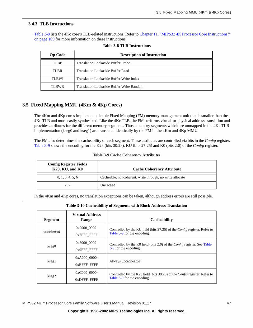
3.5 Fixed Mapping MMU (4Km & 4Kp Cores)
,”
n theand
Kc TLB
3.4.3 TLB Instructions
Table 3-8lists the 4Kc core’s TLB-related instructions. Refer toChapter 11, “MIPS32 4K Processor Core Instructionson page 169 for more information on these instructions.
3.5 Fixed Mapping MMU (4Km & 4Kp Cores)
The 4Km and 4Kp cores implement a simple Fixed Mapping (FM) memory management unit that is smaller tha4Kc TLB and more easily synthesized. Like the 4Kc TLB, the FM performs virtual-to-physical address translationprovides attributes for the different memory segments. Those memory segments which are unmapped in the 4implementation (kseg0 and kseg1) are translated identically by the FM in the 4Km and 4Kp MMU.
The FM also determines the cacheability of each segment. These attributes are controlled via bits in theConfigregister.Table 3-9 shows the encoding for the K23 (bits 30:28), KU (bits 27:25) and K0 (bits 2:0) of theConfig register.
In the 4Km and 4Kp cores, no translation exceptions can be taken, although address errors are still possible.C
Table 3-8 TLB Instructions
Op Code Description of Instruction
TLBP Translation Lookaside Buffer Probe
TLBR Translation Lookaside Buffer Read
TLBWI Translation Lookaside Buffer Write Index
TLBWR Translation Lookaside Buffer Write Random
Table 3-9 Cache Coherency Attributes
Config Register FieldsK23, KU, and K0 Cache Coherency Attribute
0, 1, 3, 4, 5, 6 Cacheable, noncoherent, write through, no write allocate
2, 7 Uncached
Table 3-10 Cacheability of Segments with Block Address Translation
SegmentVirtual Address
Range Cacheability
useg/kuseg0x0000_0000-
0x7FFF_FFFF
Controlled by the KU field (bits 27:25) of theConfigregister. Refer toTable 3-9 for the encoding.
kseg00x8000_0000-
0x9FFF_FFFF
Controlled by the K0 field (bits 2:0) of theConfig register. SeeTable3-9 for the encoding.
kseg10xA000_0000-
0xBFFF_FFFFAlways uncacheable
kseg20xC000_0000-
0xDFFF_FFFF
Controlled by the K23 field (bits 30:28) of theConfigregister. Refer toTable 3-9 for the encoding.
MIPS32 4K™ Processor Core Family Software User’s Manual, Revision 01.17 47
Copyright © 1998-2002 MIPS Technologies Inc. All rights reserved.

Chapter 3 Memory Management
own inif there
ase see
The FM performs a simple translation to map from virtual addresses to physical addresses. This mapping is shFigure 3-11. When ERL=1, useg and kuseg become unmapped and uncached. The ERL behavior is the same aswas a JTLB. The ERL mapping is shown inFigure 3-12.
The ERL bit is usually never asserted by software. It is asserted by hardware after a Reset, SoftReset or NMI. PleSection 4.6, "Exceptions" on page 56 for further information on exceptions.
Figure 3-11 FM Memory Map (ERL=0) in the 4Km and 4Kp Processor Cores
kseg30xE000_0000-
0xFFFF_FFFF
Controlled by K23 field (bits 30:28) of theConfig register. Refer toTable 3-9 for the encoding.
Table 3-10 Cacheability of Segments with Block Address Translation
SegmentVirtual Address
Range Cacheability
useg/kuseg
useg/kuseg
Virtual Address Physical Address
kseg3
kseg2
kseg1
kseg0
kseg3
kseg2
reserved
kseg0/kseg1
0xE000_0000
0xC000_0000
0xA000_0000
0x8000_0000
0x0000_0000
0xE000_0000
0xC000_0000
0x0000_0000
0x2000_0000
0x4000_0000
48 MIPS32 4K™ Processor Core Family Software User’s Manual, Revision 01.17
Copyright © 1998-2002 MIPS Technologies Inc. All rights reserved.

3.6 System Control Coprocessor
portssters are
Figure 3-12 FM Memory Map (ERL=1) in the 4Km and 4Kp Processor Cores
3.6 System Control Coprocessor
The System Control Coprocessor (CP0) is implemented as an integral part of the 4K processor cores and supmemory management, address translation, exception handling, and other privileged operations. Certain CP0 regiused to support memory management. Refer toChapter 5, “CP0 Registers,” on page 73for more information on the CP0register set.
0xE000_0000
Physical AddressVirtual Address
kseg3
0xE000_0000
kseg3
kseg2kseg2
0xC000_00000xC000_0000
0xA000_0000
kseg1
reserved
0x8000_00000x8000_0000
kseg0
useg/kuseguseg/kuseg
0x2000_0000
0x0000_00000x0000_0000
kseg0/kseg1
MIPS32 4K™ Processor Core Family Software User’s Manual, Revision 01.17 49
Copyright © 1998-2002 MIPS Technologies Inc. All rights reserved.
Chapter 3 Memory Management
50 MIPS32 4K™ Processor Core Family Software User’s Manual, Revision 01.17
Copyright © 1998-2002 MIPS Technologies Inc. All rights reserved.

sidets oneel mode.
andler)counter,
an be
branchin the
elled.re
ns thatith thear the
ctionstay itself
Chapter 4
Exceptions
All The MIPS32 4K processor cores receives exceptions from a number of sources, including translation lookabuffer (TLB) misses (4Kc core only), arithmetic overflows, I/O interrupts, and system calls. When the CPU detecof these exceptions, the normal sequence of instruction execution is suspended and the processor enters kern
In kernel mode, the core disables interrupts and forces execution of a software exception processor (called a hlocated at a fixed address. The handler saves the context of the processor, including the contents of the programthe current operating mode, and the status of the interrupts (enabled or disabled). This context is saved so it crestored when the exception has been serviced.
When an exception occurs, the core loads theException Program Counter (EPC) register with a location whereexecution can restart after the exception has been serviced. The restart location in theEPCregister is the address of theinstruction that caused the exception or, if the instruction was executing in a branch delay slot, the address of theinstruction immediately preceding the delay slot. To distinguish between the two, software must read the BD bitCP0Cause register.
This chapter contains the following sections:
• Section 4.1, "Exception Conditions"
• Section 4.2, "Exception Priority"
• Section 4.3, "Exception Vector Locations"
• Section 4.4, "General Exception Processing"
• Section 4.5, "Debug Exception Processing"
• Section 4.6, "Exceptions"
• Section 4.7, "Exception Handling and Servicing Flowcharts"
4.1 Exception Conditions
When an exception condition occurs, the relevant instruction and all those that follow it in the pipeline are cancAccordingly, any stall conditions and any later exception conditions that may have referenced this instruction ainhibited; there is no benefit in servicing stalls for a cancelled instruction.
When an exception condition is detected on an instruction fetch, the core aborts that instruction and all instructiofollow. When this instruction reaches the W stage, the exception flag causes it to write various CP0 registers wexception state, change the current program counter (PC) to the appropriate exception vector address, and cleexception bits of earlier pipeline stages.
This implementation allows all preceding instructions to complete execution and prevents all subsequent instrufrom completing. Thus, the value in theEPC(ErrorEPC for errors orDEPCfor debug exceptions) is sufficient to restarexecution. It also ensures that exceptions are taken in the order of execution; an instruction taking an exception mbe killed by an instruction further down the pipeline that takes an exception in a later cycle.
MIPS32 4K™ Processor Core Family Software User’s Manual, Revision 01.17 51
Copyright © 1998-2002 MIPS Technologies Inc. All rights reserved.

Chapter 4 Exceptions
ns can
4.2 Exception Priority
Table 4-1lists all possible exceptions and the relative priority of each, highest to lowest. Several of these exceptiohappen simultaneously, in that event the exception with the highest priority is the one taken.
Table 4-1 Priority of Exceptions
Exception Description
Reset Assertion of SI_ColdReset signal.
Soft Reset Assertion of SI_Reset signal.
DSS EJTAG Debug Single Step.
DINT EJTAG Debug Interrupt. Caused by the assertion of the external EJ_DINTinput, or by setting the EjtagBrk bit in theECR register.
NMI Asserting edge of SI_NMI signal.
Machine Check TLB write that conflicts with an existing entry (4Kc core).
Interrupt Assertion of unmasked HW or SW interrupt signal.
Deferred Watch Deferred Watch (unmasked by K|DM->!(K|DM) transition).
DIB EJTAG debug hardware instruction break matched.
WATCH A reference to an address in one of the watch registers (fetch).
AdELFetch address alignment error.
User mode fetch reference to kernel address.
TLBLFetch TLB miss (4Kc core).
Fetch TLB hit to page with V=0 (4Kc core).
IBE Instruction fetch bus error.
DBp EJTAG Breakpoint (execution of SDBBP instruction).
Sys Execution of SYSCALL instruction.
Bp Execution of BREAK instruction.
CpU Execution of a coprocessor instruction for a coprocessor that is not enabled.
RI Execution of a Reserved Instruction.
Ov Execution of an arithmetic instruction that overflowed.
Tr Execution of a trap (when trap condition is true).
DDBL / DDBS EJTAG Data Address Break (address only) or EJTAG Data Value Break onStore (address and value).
WATCH A reference to an address in one of the watch registers (data).
AdELLoad address alignment error.
User mode load reference to kernel address.
AdESStore address alignment error.
User mode store to kernel address.
52 MIPS32 4K™ Processor Core Family Software User’s Manual, Revision 01.17
Copyright © 1998-2002 MIPS Technologies Inc. All rights reserved.
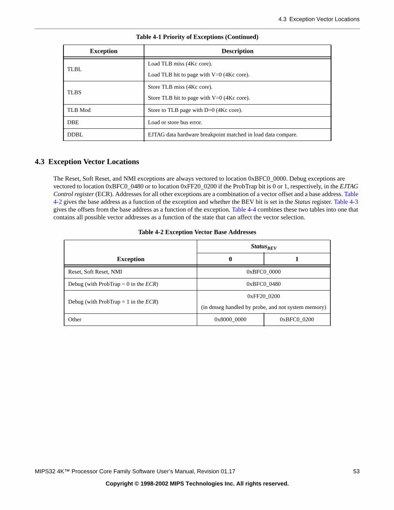
4.3 Exception Vector Locations
are
.
t
4.3 Exception Vector Locations
The Reset, Soft Reset, and NMI exceptions are always vectored to location 0xBFC0_0000. Debug exceptions vectored to location 0xBFC0_0480 or to location 0xFF20_0200 if the ProbTrap bit is 0 or 1, respectively, in theEJTAGControl register(ECR). Addresses for all other exceptions are a combination of a vector offset and a base addressTable4-2gives the base address as a function of the exception and whether the BEV bit is set in theStatusregister.Table 4-3gives the offsets from the base address as a function of the exception.Table 4-4combines these two tables into one thacontains all possible vector addresses as a function of the state that can affect the vector selection.
TLBLLoad TLB miss (4Kc core).
Load TLB hit to page with V=0 (4Kc core).
TLBSStore TLB miss (4Kc core).
Store TLB hit to page with V=0 (4Kc core).
TLB Mod Store to TLB page with D=0 (4Kc core).
DBE Load or store bus error.
DDBL EJTAG data hardware breakpoint matched in load data compare.
Table 4-2 Exception Vector Base Addresses
Exception
StatusBEV
0 1
Reset, Soft Reset, NMI 0xBFC0_0000
Debug (with ProbTrap = 0 in theECR) 0xBFC0_0480
Debug (with ProbTrap = 1 in theECR)0xFF20_0200
(in dmseg handled by probe, and not system memory)
Other 0x8000_0000 0xBFC0_0200
Table 4-1 Priority of Exceptions (Continued)
Exception Description
MIPS32 4K™ Processor Core Family Software User’s Manual, Revision 01.17 53
Copyright © 1998-2002 MIPS Technologies Inc. All rights reserved.

Chapter 4 Exceptions
as
,
CE
4.4 General Exception Processing
With the exception of Reset, Soft Reset, NMI, and Debug exceptions, which have their own special processingdescribed below, exceptions have the same basic processing flow:
• If the EXL bit in theStatus register is cleared, theEPC register is loaded with the PC at which execution will berestarted and the BD bit is set appropriately in theCauseregister. If the instruction is not in the delay slot of a branchthe BD bit inCause will be cleared and the value loaded into theEPC register is the current PC. If the instruction isin the delay slot of a branch, the BD bit inCause is set andEPC is loaded with PC-4. If the EXL bit in theStatusregister is set, theEPC register is not loaded and the BD bit is not changed in theCause register.
• The CE and ExcCode fields of theCause registers are loaded with the values appropriate to the exception. The field is loaded, but not defined, for any exception type other than a coprocessor unusable exception.
• The EXL bit is set in theStatus register.
Table 4-3 Exception Vector Offsets
Exception Vector Offset
TLB refill, EXL = 0 (4Kc core) 0x000
Reset, Soft Reset, NMI 0x000 (uses reset base address)
General Exception 0x180
Interrupt,CauseIV = 1 0x200
Table 4-4 Exception Vectors
Exception BEV EXL IVEJTAG
ProbTrap Vector
Reset, Soft Reset, NMI x x x x 0xBFC0_0000
Debug x x x 0 0xBFC0_0480
Debug x x x 1 0xFF20_0200 (in dmseg)
TLB Refill (4Kc core) 0 0 x x 0x8000_0000
TLB Refill (4Kc core) 0 1 x x 0x8000_0180
TLB Refill (4Kc core) 1 0 x x 0xBFC0_0200
TLB Refill (4Kc core) 1 1 x x 0xBFC0_0380
Interrupt 0 0 0 x 0x8000_0180
Interrupt 0 0 1 x 0x8000_0200
Interrupt 1 0 0 x 0xBFC0_0380
Interrupt 1 0 1 x 0xBFC0_0400
All others 0 x x x 0x8000_0180
All others 1 x x x 0xBFC0_0380
Note: ‘x’ denotes don’t care
54 MIPS32 4K™ Processor Core Family Software User’s Manual, Revision 01.17
Copyright © 1998-2002 MIPS Technologies Inc. All rights reserved.

4.5 Debug Exception Processing
andler
iption
DBD
f a
• The processor is started at the exception vector.
The value loaded intoEPCrepresents the restart address for the exception and need not be modified by exception hsoftware in the normal case. Software need not look at the BD bit in theCause register unless is wishes to identify theaddress of the instruction that actually caused the exception.
Note that individual exception types may load additional information into other registers. This is noted in the descrof each exception type below.
Operation:
if Status EXL = 0 thenif InstructionInBranchDelaySlot then
EPC <- PC - 4CauseBD <- 1
elseEPC <- PCCauseBD <- 0
endifif ExceptionType = TLBRefill then
vectorOffset <- 0x000elseif (ExceptionType = Interrupt) and(Cause IV = 1) then
vectorOffset <- 0x200else
vectorOffset <- 0x180endif
elsevectorOffset <- 0x180
endifCauseCE <- FaultingCoprocessorNumberCauseExcCode <- ExceptionTypeStatus EXL <- 1if Status BEV = 1 then
PC <- 0xBFC0_0200 + vectorOffsetelse
PC <- 0x8000_0000 + vectorOffsetendif
4.5 Debug Exception Processing
All debug exceptions have the same basic processing flow:
• TheDEPCregister is loaded with the program counter (PC) value at which execution will be restarted and thebit is set appropriately in theDebug register. The value loaded into theDEPC register is the current PC if theinstruction is not in the delay slot of a branch, or the PC-4 of the branch if the instruction is in the delay slot obranch.
• The DSS, DBp, DDBL, DDBS, DIB and DINT bits (D* bits at [5:0]) in theDebugregister are updated appropriatelydepending on the debug exception type.
• Halt and Doze bits in theDebug register are updated appropriately.
• DM bit in theDebug register is set to 1.
• The processor is started at the debug exception vector.
MIPS32 4K™ Processor Core Family Software User’s Manual, Revision 01.17 55
Copyright © 1998-2002 MIPS Technologies Inc. All rights reserved.
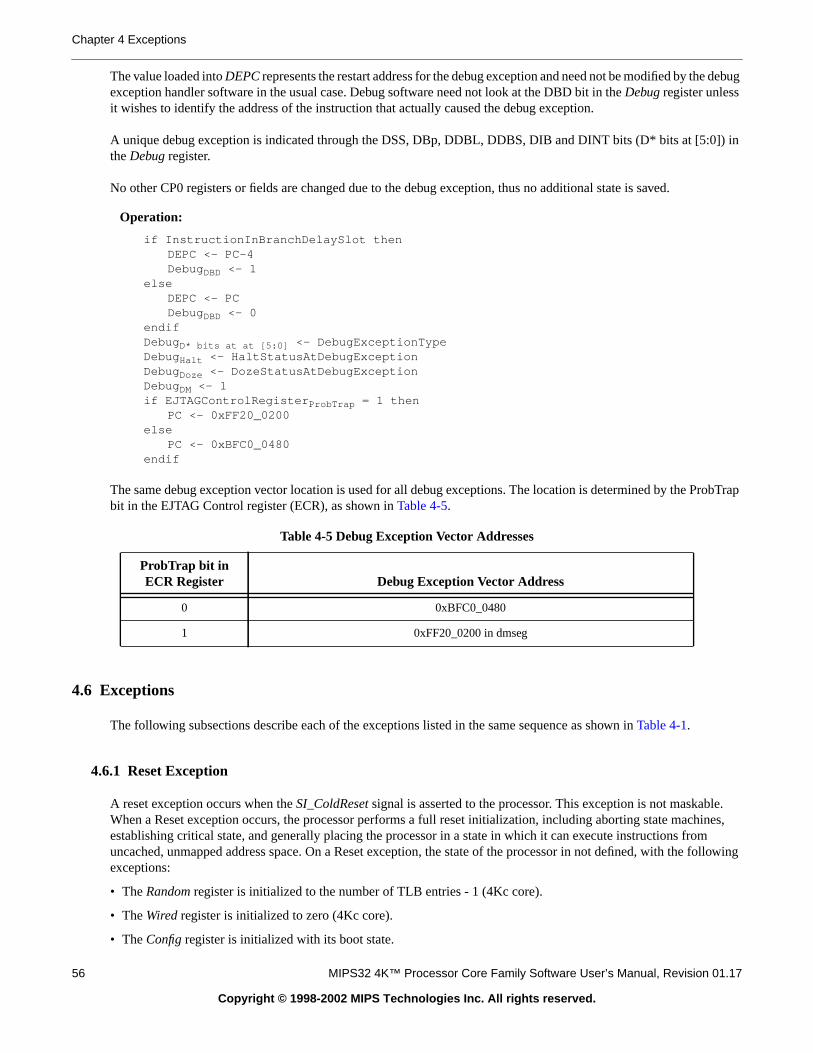
Chapter 4 Exceptions
debug
) in
obTrap
e.ines,m following
The value loaded intoDEPCrepresents the restart address for the debug exception and need not be modified by theexception handler software in the usual case. Debug software need not look at the DBD bit in theDebugregister unlessit wishes to identify the address of the instruction that actually caused the debug exception.
A unique debug exception is indicated through the DSS, DBp, DDBL, DDBS, DIB and DINT bits (D* bits at [5:0]theDebugregister.
No other CP0 registers or fields are changed due to the debug exception, thus no additional state is saved.
Operation:
if InstructionInBranchDelaySlot thenDEPC <- PC-4DebugDBD <- 1
elseDEPC <- PCDebugDBD <- 0
endifDebugD* bits at at [5:0] <- DebugExceptionTypeDebugHalt <- HaltStatusAtDebugExceptionDebugDoze <- DozeStatusAtDebugExceptionDebugDM <- 1if EJTAGControlRegister ProbTrap = 1 then
PC <- 0xFF20_0200else
PC <- 0xBFC0_0480endif
The same debug exception vector location is used for all debug exceptions. The location is determined by the Prbit in the EJTAG Control register (ECR), as shown inTable 4-5.
4.6 Exceptions
The following subsections describe each of the exceptions listed in the same sequence as shown inTable 4-1.
4.6.1 Reset Exception
A reset exception occurs when theSI_ColdReset signal is asserted to the processor. This exception is not maskablWhen a Reset exception occurs, the processor performs a full reset initialization, including aborting state machestablishing critical state, and generally placing the processor in a state in which it can execute instructions frouncached, unmapped address space. On a Reset exception, the state of the processor in not defined, with theexceptions:
• TheRandom register is initialized to the number of TLB entries - 1 (4Kc core).
• TheWired register is initialized to zero (4Kc core).
• TheConfig register is initialized with its boot state.
Table 4-5 Debug Exception Vector Addresses
ProbTrap bit inECR Register Debug Exception Vector Address
0 0xBFC0_0480
1 0xFF20_0200 in dmseg
56 MIPS32 4K™ Processor Core Family Software User’s Manual, Revision 01.17
Copyright © 1998-2002 MIPS Technologies Inc. All rights reserved.

4.6 Exceptions
uction
henet the cache, orent. In
uction
• The RP, BEV, TS, SR, NMI, and ERL fields of theStatus register are initialized to a specified state.
• The I, R, and W fields of theWatchLo register are initialized to 0.
• TheErrorEPC register is loaded with PC-4 if the state of the processor indicates that it was executing an instrin the delay slot of a branch. Otherwise, theErrorEPC register is loaded with PC. Note that this value may or maynot be predictable.
• PC is loaded with 0xBFC0_0000.
Cause Register ExcCode Value:
None
Additional State Saved:
None
Entry Vector Used:
Reset (0xBFC0_0000)
Operation:
Random <- TLBEntries - 1Wired <- 0Config <- ConfigurationStateStatus RP <- 0Status BEV <- 1Status TS <- 0Status SR <- 0Status NMI <- 0Status ERL <- 1WatchLo I <- 0WatchLo R <- 0WatchLo W <- 0if InstructionInBranchDelaySlot then
ErrorEPC <- PC - 4else
ErrorEPC <- PCendifPC <- 0xBFC0_0000
4.6.2 Soft Reset Exception
A soft reset exception occurs when theSI_Resetsignal is asserted to the processor. This exception is not maskable. Wa soft reset exception occurs, the processor performs a subset of the full reset initialization. Although a soft resexception does not unnecessarily change the state of the processor, it may be forced to do so in order to placeprocessor in a state in which it can execute instructions from uncached, unmapped address space. Since bus,other operations may be interrupted, portions of the cache, memory, or other processor state may be inconsistaddition to any hardware initialization required, the following state is established on a soft reset exception:
• The BEV, TS, SR, NMI, and ERL fields of theStatus register are initialized to a specified state.
• TheErrorEPC register is loaded with PC-4 if the state of the processor indicates that it was executing an instrin the delay slot of a branch. Otherwise, theErrorEPC register is loaded with PC. Note that this value may or maynot be predictable.
• PC is loaded with 0xBFC0_0000.
Cause Register ExcCode Value:
None
MIPS32 4K™ Processor Core Family Software User’s Manual, Revision 01.17 57
Copyright © 1998-2002 MIPS Technologies Inc. All rights reserved.

Chapter 4 Exceptions
en
tion in register,
he nextctioner set step.
houghtaken onturning
tion, ande the
ons,
Additional State Saved:
None
Entry Vector Used:
Reset (0xBFC0_0000)
Operation:
Status BEV <- 1Status TS <- 0Status SR <- 1Status NMI <- 0Status ERL <- 1if InstructionInBranchDelaySlot then
ErrorEPC <- PC - 4else
ErrorEPC <- PCendifPC <- 0xBFC0_0000
4.6.3 Debug Single Step Exception
A debug single step exception occurs after the CPU has executed one/two instructions in non-debug mode, whreturning to non-debug mode after debug mode. One instruction is allowed to execute when returning to a nonjump/branch instruction, otherwise two instructions are allowed to execute since the jump/branch and the instructhe delay slot are executed as one step. Debug single step exceptions are enabled by the SSt bit in the Debugand are always disabled for the first one/two instructions after a DERET.
The DEPC register points to the instruction on which the debug single step exception occurred, which is also tinstruction to single step or execute when returning from debug mode. So the DEPC will not point to the instruwhich has just been single stepped, but rather the following instruction. The DBD bit in the Debug register is nevfor a debug single step exception, since the jump/branch and the instruction in the delay slot is executed in one
Exceptions occurring on the instruction(s) executed with debug single step exception enabled are taken even tdebug single step was enabled. For a normal exception (other than reset), a debug single step exception is thenthe first instruction in the normal exception handler. Debug exceptions are unaffected by single step mode, e.g. reto a SDBBP instruction with debug single step exceptions enabled causes a debug software breakpoint excepthe DEPC will point to the SDBBP instruction. However, returning to an instruction (not jump/branch) just beforSDBBP instruction, causes a debug single step exception with the DEPC pointing to the SDBBP instruction.
To ensure proper functionality of single step, the debug single step exception has priority over all other exceptiexcept reset and soft reset.
Debug Register Debug Status Bit Set
DSS
Additional State Saved
None
Entry Vector Used
Debug exception vector
58 MIPS32 4K™ Processor Core Family Software User’s Manual, Revision 01.17
Copyright © 1998-2002 MIPS Technologies Inc. All rights reserved.

4.6 Exceptions
th noueg in the
temory,
uction
4.6.4 Debug Interrupt Exception
A debug interrupt exception is either caused by the EjtagBrk bit in theEJTAG Control register (controlled through theTAP), or caused by the debug interrupt request signal to the CPU.
The debug interrupt exception is an asynchronous debug exception which is taken as soon as possible, but wispecific relation to the executed instructions. TheDEPCregister is set to the instruction where execution should continafter the debug handler is through. The DBD bit is set based on whether the interrupted instruction was executindelay slot of a branch.
Debug Register Debug Status Bit Set
DINT
Additional State Saved
None
Entry Vector Used
Debug exception vector
4.6.5 Non-Maskable Interrupt (NMI) Exception
A non-maskable interrupt exception occurs when theSI_NMIsignal is asserted to the processor.SI_NMI is an edgesensitive signal - only one NMI exception will be taken each time it is asserted. An NMI exception occurs only ainstruction boundaries, so it does not cause any reset or other hardware initialization. The state of the cache, mand other processor states are consistent and all registers are preserved, with the following exceptions:
• The BEV, TS, SR, NMI, and ERL fields of theStatus register are initialized to a specified state.
• TheErrorEPC register is loaded with PC-4 if the state of the processor indicates that it was executing an instrin the delay slot of a branch. Otherwise, theErrorEPC register is loaded with PC.
• PC is loaded with 0xBFC0_0000.
Cause Register ExcCode Value:
None
Additional State Saved:
None
Entry Vector Used:
Reset (0xBFC0_0000)
Operation:
Status BEV <- 1Status TS <- 0Status SR <- 0Status NMI <- 1Status ERL <- 1if InstructionInBranchDelaySlot then
ErrorEPC <- PC - 4else
ErrorEPC <- PCendifPC <- 0xBFC0_0000
MIPS32 4K™ Processor Core Family Software User’s Manual, Revision 01.17 59
Copyright © 1998-2002 MIPS Technologies Inc. All rights reserved.
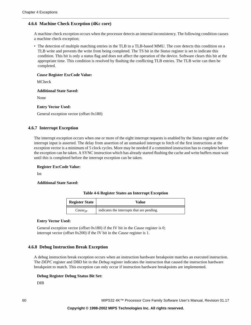
Chapter 4 Exceptions
causes
n a
t at thee
t thebeforest wait
ruction.e
4.6.6 Machine Check Exception (4Kc core)
A machine check exception occurs when the processor detects an internal inconsistency. The following conditiona machine check exception;
• The detection of multiple matching entries in the TLB in a TLB-based MMU. The core detects this condition oTLB write and prevents the write from being completed. The TS bit in theStatus register is set to indicate thiscondition. This bit is only a status flag and does not affect the operation of the device. Software clears this biappropriate time. This condition is resolved by flushing the conflicting TLB entries. The TLB write can then bcompleted.
Cause Register ExcCode Value:
MCheck
Additional State Saved:
None
Entry Vector Used:
General exception vector (offset 0x180)
4.6.7 Interrupt Exception
The interrupt exception occurs when one or more of the eight interrupt requests is enabled by theStatusregister and theinterrupt input is asserted. The delay from assertion of an unmasked interrupt to fetch of the first instructions aexception vector is a minimum of 5 clock cycles. More may be needed if a committed instruction has to completethe exception can be taken. A SYNC instruction which has already started flushing the cache and write buffers muuntil this is completed before the interrupt exception can be taken.
Register ExcCode Value:
Int
Additional State Saved:
Entry Vector Used:
General exception vector (offset 0x180) if the IV bit in theCause register is 0;interrupt vector (offset 0x200) if the IV bit in theCause register is 1.
4.6.8 Debug Instruction Break Exception
A debug instruction break exception occurs when an instruction hardware breakpoint matches an executed instTheDEPC register and DBD bit in theDebug register indicates the instruction that caused the instruction hardwarbreakpoint to match. This exception can only occur if instruction hardware breakpoints are implemented.
Debug Register Debug Status Bit Set:
DIB
Table 4-6 Register States an Interrupt Exception
Register State Value
CauseIP indicates the interrupts that are pending.
60 MIPS32 4K™ Processor Core Family Software User’s Manual, Revision 01.17
Copyright © 1998-2002 MIPS Technologies Inc. All rights reserved.
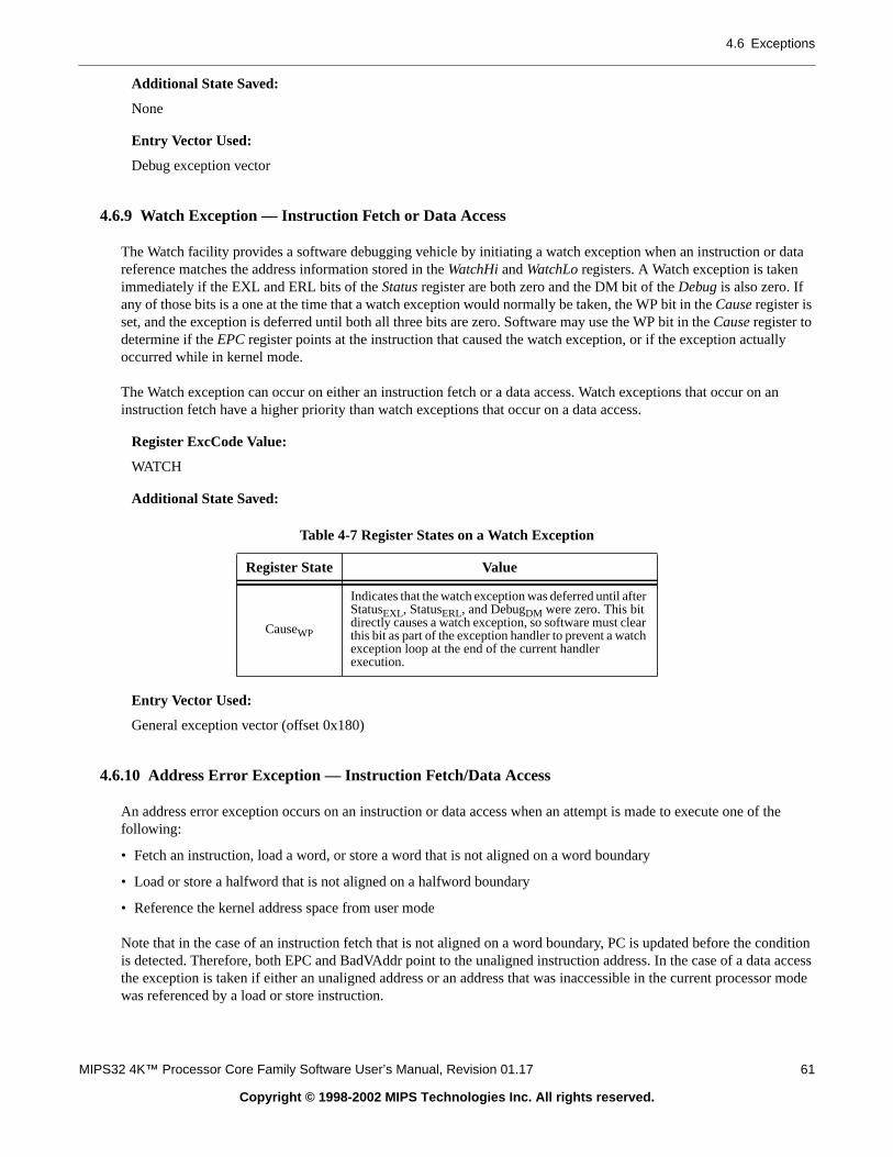
4.6 Exceptions
data
ly
an
f the
onditionaccess
sor mode
Additional State Saved:
None
Entry Vector Used:
Debug exception vector
4.6.9 Watch Exception — Instruction Fetch or Data Access
The Watch facility provides a software debugging vehicle by initiating a watch exception when an instruction orreference matches the address information stored in theWatchHi andWatchLo registers. A Watch exception is takenimmediately if the EXL and ERL bits of theStatus register are both zero and the DM bit of theDebugis also zero. Ifany of those bits is a one at the time that a watch exception would normally be taken, the WP bit in theCauseregister isset, and the exception is deferred until both all three bits are zero. Software may use the WP bit in theCauseregister todetermine if theEPC register points at the instruction that caused the watch exception, or if the exception actualoccurred while in kernel mode.
The Watch exception can occur on either an instruction fetch or a data access. Watch exceptions that occur oninstruction fetch have a higher priority than watch exceptions that occur on a data access.
Register ExcCode Value:
WATCH
Additional State Saved:
Entry Vector Used:
General exception vector (offset 0x180)
4.6.10 Address Error Exception — Instruction Fetch/Data Access
An address error exception occurs on an instruction or data access when an attempt is made to execute one ofollowing:
• Fetch an instruction, load a word, or store a word that is not aligned on a word boundary
• Load or store a halfword that is not aligned on a halfword boundary
• Reference the kernel address space from user mode
Note that in the case of an instruction fetch that is not aligned on a word boundary, PC is updated before the cis detected. Therefore, both EPC and BadVAddr point to the unaligned instruction address. In the case of a datathe exception is taken if either an unaligned address or an address that was inaccessible in the current proceswas referenced by a load or store instruction.
Table 4-7 Register States on a Watch Exception
Register State Value
CauseWP
Indicates that the watch exception was deferred until afterStatusEXL, StatusERL, and DebugDM were zero. This bitdirectly causes a watch exception, so software must clearthis bit as part of the exception handler to prevent a watchexception loop at the end of the current handlerexecution.
MIPS32 4K™ Processor Core Family Software User’s Manual, Revision 01.17 61
Copyright © 1998-2002 MIPS Technologies Inc. All rights reserved.
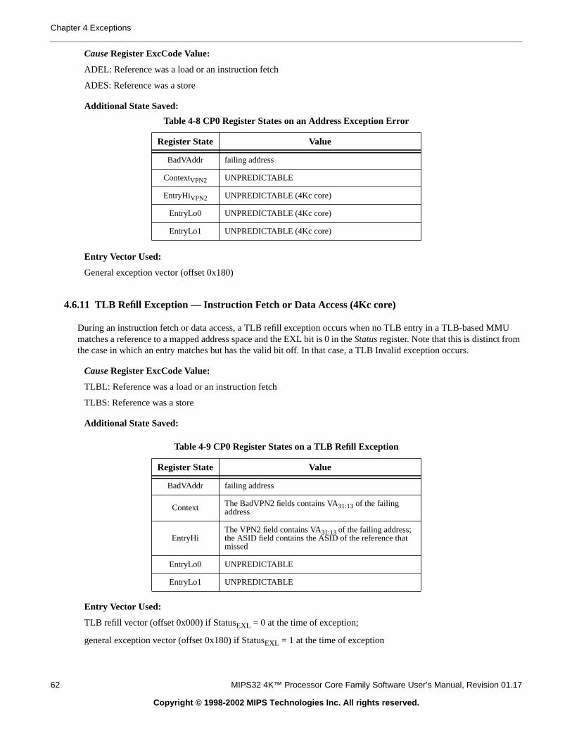
Chapter 4 Exceptions
U
Cause Register ExcCode Value:
ADEL: Reference was a load or an instruction fetch
ADES: Reference was a store
Additional State Saved:
Entry Vector Used:
General exception vector (offset 0x180)
4.6.11 TLB Refill Exception — Instruction Fetch or Data Access (4Kc core)
During an instruction fetch or data access, a TLB refill exception occurs when no TLB entry in a TLB-based MMmatches a reference to a mapped address space and the EXL bit is 0 in theStatusregister. Note that this is distinct fromthe case in which an entry matches but has the valid bit off. In that case, a TLB Invalid exception occurs.
Cause Register ExcCode Value:
TLBL: Reference was a load or an instruction fetch
TLBS: Reference was a store
Additional State Saved:
Entry Vector Used:
TLB refill vector (offset 0x000) if StatusEXL = 0 at the time of exception;
general exception vector (offset 0x180) if StatusEXL = 1 at the time of exception
Table 4-8 CP0 Register States on an Address Exception Error
Register State Value
BadVAddr failing address
ContextVPN2 UNPREDICTABLE
EntryHiVPN2 UNPREDICTABLE (4Kc core)
EntryLo0 UNPREDICTABLE (4Kc core)
EntryLo1 UNPREDICTABLE (4Kc core)
Table 4-9 CP0 Register States on a TLB Refill Exception
Register State Value
BadVAddr failing address
Context The BadVPN2 fields contains VA31:13 of the failingaddress
EntryHiThe VPN2 field contains VA31:13of the failing address;the ASID field contains the ASID of the reference thatmissed
EntryLo0 UNPREDICTABLE
EntryLo1 UNPREDICTABLE
62 MIPS32 4K™ Processor Core Family Software User’s Manual, Revision 01.17
Copyright © 1998-2002 MIPS Technologies Inc. All rights reserved.

4.6 Exceptions
the
as the
anstructionrror
rs, suchrycle.
4.6.12 TLB Invalid Exception — Instruction Fetch or Data Access (4Kc core)
During an instruction fetch or data access, a TLB invalid exception occurs in one of the following cases:
• No TLB entry in a TLB-based MMU matches a reference to a mapped address space; and the EXL bit is 1 inStatus register.
• A TLB entry in a TLB-based MMU matches a reference to a mapped address space, but the matched entry hvalid bit off.
• The virtual address is greater than or equal to the bounds address in a FM-based MMU.
Cause Register ExcCode Value:
TLBL: Reference was a load or an instruction fetch
TLBS: Reference was a store
Additional State Saved:
Entry Vector Used:
General exception vector (offset 0x180)
4.6.13 Bus Error Exception — Instruction Fetch or Data Access
A bus error exception occurs when an instruction or data access makes a bus request (due to a cache miss oruncacheable reference) and that request terminates in an error. The bus error exception can occur on either an infetch or a data access. Bus error exceptions that occur on an instruction fetch have a higher priority than bus eexceptions that occur on a data access.
Bus errors taken on the requested (critical) word of an instruction fetch or data load are precise. Other bus erroas stores or non-critical words of a burst read, can be imprecise. These errors are taken when the EB_RBErr oEB_WBErr signals are asserted and may occur on an instruction that was not the source of the offending bus c
Cause Register ExcCode Value:
IBE: Error on an instruction reference
DBE: Error on a data reference
Additional State Saved:
None
Table 4-10 CP0 Register States on a TLB Invalid Exception
Register State Value
BadVAddr failing address
Context The BadVPN2 field contains VA31:13 of the failingaddress
EntryHiThe VPN2 field contains VA31:13 of the failing address;the ASID field contains the ASID of the reference thatmissed
EntryLo0 UNPREDICTABLE
EntryLo1 UNPREDICTABLE
MIPS32 4K™ Processor Core Family Software User’s Manual, Revision 01.17 63
Copyright © 1998-2002 MIPS Technologies Inc. All rights reserved.
Chapter 4 Exceptions
system
. A
priority.ed.
Entry Vector Used:
General exception vector (offset 0x180)
4.6.14 Debug Software Breakpoint Exception
A debug software breakpoint exception occurs when an SDBBP instruction is executed. TheDEPC register and DBDbit in theDebug register will indicate the SDBBP instruction that caused the debug exception.
Debug Register Debug Status Bit Set:
DBp
Additional State Saved:
None
Entry Vector Used:
Debug exception vector
4.6.15 Execution Exception — System Call
The system call exception is one of the six execution exceptions. All of these exceptions have the same priority. Acall exception occurs when a SYSCALL instruction is executed.
Cause Register ExcCode Value:
Sys
Additional State Saved:
None
Entry Vector Used:
General exception vector (offset 0x180)
4.6.16 Execution Exception — Breakpoint
The breakpoint exception is one of the six execution exceptions. All of these exceptions have the same prioritybreakpoint exception occurs when a BREAK instruction is executed.
Cause Register ExcCode Value:
Bp
Additional State Saved:
None
Entry Vector Used:
General exception vector (offset 0x180)
4.6.17 Execution Exception — Reserved Instruction
The reserved instruction exception is one of the six execution exceptions. All of these exceptions have the sameA reserved instruction exception occurs when a reserved or undefined major opcode or function field is execut
64 MIPS32 4K™ Processor Core Family Software User’s Manual, Revision 01.17
Copyright © 1998-2002 MIPS Technologies Inc. All rights reserved.

4.6 Exceptions
amefor one
ity. An
eption
Cause Register ExcCode Value:
RI
Additional State Saved:
None
Entry Vector Used:
General exception vector (offset 0x180)
4.6.18 Execution Exception — Coprocessor Unusable
The coprocessor unusable exception is one of the six execution exceptions. All of these exceptions have the spriority. A coprocessor unusable exception occurs when an attempt is made to execute a coprocessor instructionof the following:
• a corresponding coprocessor unit that has not been marked usable by setting its CU bit in theStatus register
• CP0 instructions, when the unit has not been marked usable, and the processor is executing in user mode
Cause Register ExcCode Value:
CpU
Additional State Saved:
Entry Vector Used:
General exception vector (offset 0x180)
4.6.19 Execution Exception — Integer Overflow
The integer overflow exception is one of the six execution exceptions. All of these exceptions have the same priorinteger overflow exception occurs when selected integer instructions result in a 2’s complement overflow.
Cause Register ExcCode Value:
Ov
Additional State Saved:
None
Entry Vector Used:
General exception vector (offset 0x180)
4.6.20 Execution Exception — Trap
The trap exception is one of the six execution exceptions. All of these exceptions have the same priority. A trap excoccurs when a trap instruction results in a TRUE value.
Table 4-11 Register States on a Coprocessor Unusable Exception
Register State Value
CauseCE unit number of the coprocessor being referenced
MIPS32 4K™ Processor Core Family Software User’s Manual, Revision 01.17 65
Copyright © 1998-2002 MIPS Technologies Inc. All rights reserved.

Chapter 4 Exceptions
executedts nothandler.
ing
Cause Register ExcCode Value:
Tr
Additional State Saved:
None
Entry Vector Used:
General exception vector (offset 0x180)
4.6.21 Debug Data Break Exception
A debug data break exception occurs when a data hardware breakpoint matches the load/store transaction of anload/store instruction. TheDEPCregister and DBD bit in theDebugregister will indicate the load/store instruction thacaused the data hardware breakpoint to match. The load/store instruction that caused the debug exception hacompleted e.g. not updated the register file, and the instruction can be re-executed after returning from the debug
Debug Register Debug Status Bit Set:
DDBL for a load instruction or DDBS for a store instruction
Additional State Saved:
None
Entry Vector Used:
Debug exception vector
4.6.22 TLB Modified Exception — Data Access (4Kc core)
During a data access, a TLB modified exception occurs on a store reference to a mapped address if the followcondition is true:
• The matching TLB entry in a TLB-based MMU is valid, but not dirty.
Cause Register ExcCode Value:
Mod
Additional State Saved:
Table 4-12 Register States on a TLB Modified Exception
Register State Value
BadVAddr failing address
Context The BadVPN2 field contains VA31:13 of the failingaddress.
EntryHiThe VPN2 field contains VA31:13 of the failing address;the ASID field contains the ASID of the reference thatmissed.
EntryLo0 UNPREDICTABLE
EntryLo1 UNPREDICTABLE
66 MIPS32 4K™ Processor Core Family Software User’s Manual, Revision 01.17
Copyright © 1998-2002 MIPS Technologies Inc. All rights reserved.

4.7 Exception Handling and Servicing Flowcharts
:
e (SW).servedust be. The
Entry Vector Used:
General exception vector (offset 0x180)
4.7 Exception Handling and Servicing Flowcharts
The remainder of this chapter contains flowcharts for the following exceptions and guidelines for their handlers
• General exceptions and their exception handler
• TLB miss exceptions and their exception handler (4Kc core)
• Reset, soft reset and NMI exceptions, and a guideline to their handler
• Debug exceptions
Generally speaking, the exceptions are handled by hardware (HW); the exceptions are then serviced by softwarNote that unexpected debug exceptions to the debug exception vector at 0xBFC0_0200 may be viewed as a reinstruction since uncontrolled execution of a SDBBP instruction caused the exception. The DERET instruction mused at return from the debug exception handler, in order to leave debug mode and return to non-debug modeDERET instruction returns to the address in theDEPC register.
MIPS32 4K™ Processor Core Family Software User’s Manual, Revision 01.17 67
Copyright © 1998-2002 MIPS Technologies Inc. All rights reserved.

Chapter 4 Exceptions
Figure 4-1 General Exception Handler (HW)
To General Exception Servicing Guidelines
=1 (bootstrap)=0 (normal)Status.BEV
To General Exception Servicing Guidelines
Comments
PC <- 0x8000_0000 + 180(unmapped, cached)
PC <- 0xBFC0_0200 + 180(unmapped, uncached)
EXL <- 1
EPC <- (PC - 4)Cause.BD <- 1
EPC <- PCCause.BD <- 0
Instr. inBr.Dly. Slot?
=0
Processor forced to KernelMode & interrupt disabled
=0
=1Check if exception within
another exception EXL
EntryHi and Context are set only forTLB Invalid, Modified, & Refillexceptions (4Kc core only). BadVAis set only for TLB Invalid, Modified,and Refill exceptions (4Kc coreonly). Note: not set on Bus Errors.
EntryHi <- VPN2, ASIDContext <- VPN2
Set Cause EXCCode,CEBadVA <- VA
Exceptions other than Reset, Soft Reset, NMI, or first-level TLB miss(4Kc core only). Note: Interrupts can be masked by IE or IMs, andWatch is masked if EXL = 1.
68 MIPS32 4K™ Processor Core Family Software User’s Manual, Revision 01.17
Copyright © 1998-2002 MIPS Technologies Inc. All rights reserved.

4.7 Exception Handling and Servicing Flowcharts
Figure 4-2 General Exception Servicing Guidelines (SW)
ERET
MTC0 -EPC,STATUS
EXL = 1
Service Code
* ERET is not allowed in the branch delay slot ofanother Jump Instruction* Processor does not execute the instructionwhich is in the ERET’s branch delay slot* PC <- EPC; EXL <- 0* LLbit <- 0
Check Cause value & Jump toappropriate Service Code
* After EXL=0, all exceptions allowed.(except interrupt if masked by IE)
(Optional - only to enable Interrupts while keepingKernel Mode)
MTC0 -Set Status bits:
UM <- 0, EXL <-0,IE<-1
MFC0 -Context, EPC, Status, Cause
* Unmapped vector so TLBMod, TLBInv, or TLBRefill exceptions not possible (4Kc core only)* EXL=1 so Watch, Interrupt exceptions disabled* OS/System to avoid all other exceptions* Only Reset, Soft Reset, NMI exceptions possible
Comments
MIPS32 4K™ Processor Core Family Software User’s Manual, Revision 01.17 69
Copyright © 1998-2002 MIPS Technologies Inc. All rights reserved.
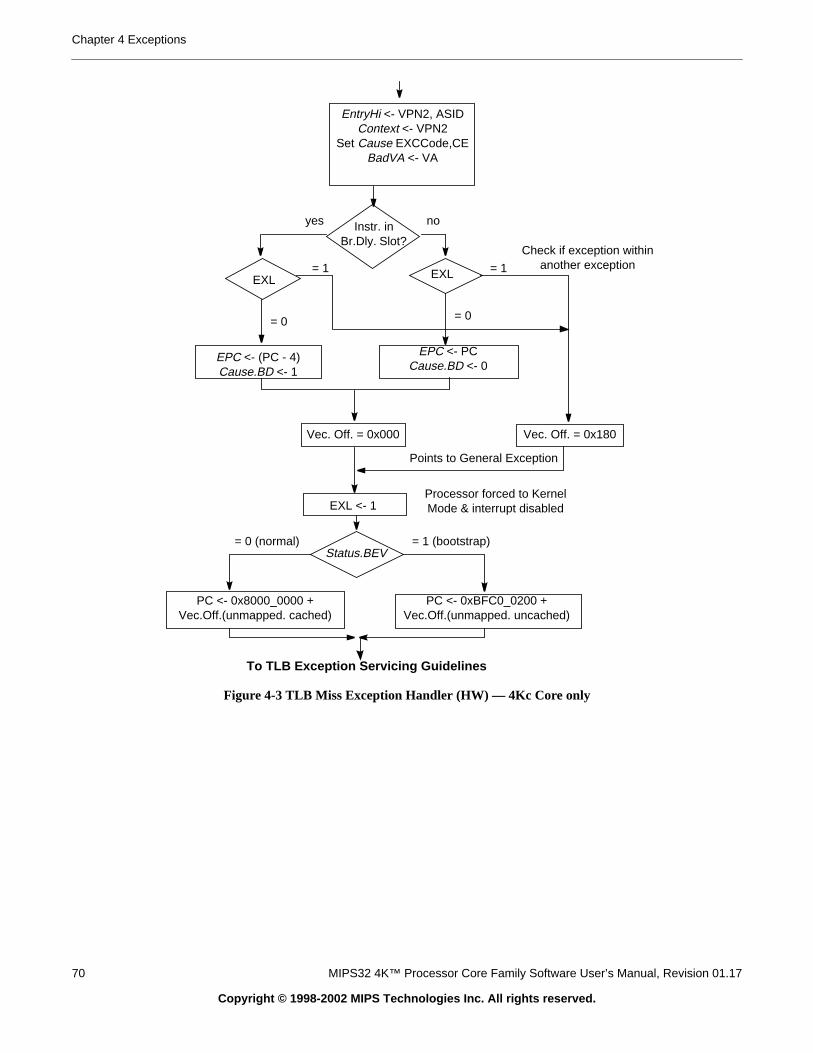
Chapter 4 Exceptions
Figure 4-3 TLB Miss Exception Handler (HW) — 4Kc Core only
To TLB Exception Servicing Guidelines
Vec. Off. = 0x180
EPC <- (PC - 4)Cause.BD <- 1
EPC <- PCCause.BD <- 0
Vec. Off. = 0x000
EXL <- 1
Points to General Exception
Processor forced to KernelMode & interrupt disabled
= 0
= 1 (bootstrap)= 0 (normal)
PC <- 0x8000_0000 +Vec.Off.(unmapped. cached)
PC <- 0xBFC0_0200 +Vec.Off.(unmapped. uncached)
Status.BEV
Check if exception withinanother exception= 1= 1
= 0
EXL EXL
EntryHi <- VPN2, ASIDContext <- VPN2
Set Cause EXCCode,CEBadVA <- VA
Instr. inBr.Dly. Slot?
noyes
70 MIPS32 4K™ Processor Core Family Software User’s Manual, Revision 01.17
Copyright © 1998-2002 MIPS Technologies Inc. All rights reserved.
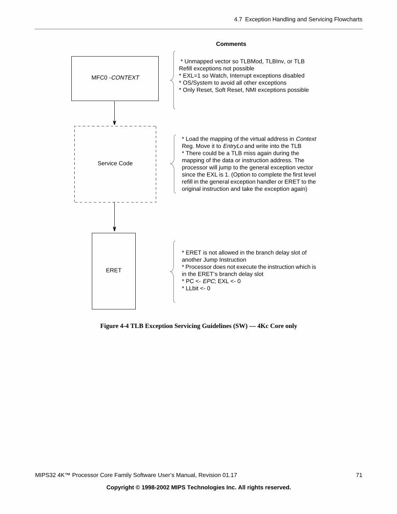
4.7 Exception Handling and Servicing Flowcharts
Figure 4-4 TLB Exception Servicing Guidelines (SW) — 4Kc Core only
Comments
ERET
Service Code
MFC0 -CONTEXT
* Unmapped vector so TLBMod, TLBInv, or TLBRefill exceptions not possible* EXL=1 so Watch, Interrupt exceptions disabled* OS/System to avoid all other exceptions* Only Reset, Soft Reset, NMI exceptions possible
* Load the mapping of the virtual address in ContextReg. Move it to EntryLo and write into the TLB* There could be a TLB miss again during themapping of the data or instruction address. Theprocessor will jump to the general exception vectorsince the EXL is 1. (Option to complete the first levelrefill in the general exception handler or ERET to theoriginal instruction and take the exception again)
* ERET is not allowed in the branch delay slot ofanother Jump Instruction* Processor does not execute the instruction which isin the ERET’s branch delay slot* PC <- EPC; EXL <- 0* LLbit <- 0
MIPS32 4K™ Processor Core Family Software User’s Manual, Revision 01.17 71
Copyright © 1998-2002 MIPS Technologies Inc. All rights reserved.
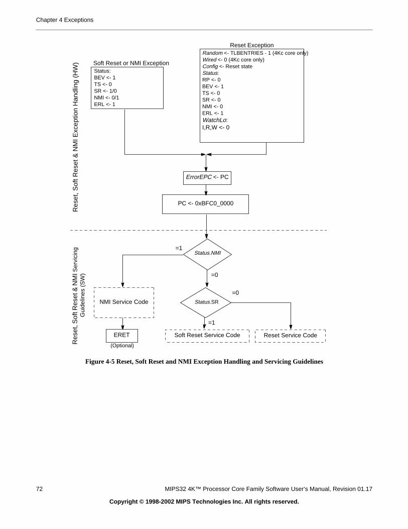
Chapter 4 Exceptions
Figure 4-5 Reset, Soft Reset and NMI Exception Handling and Servicing Guidelines
Status:BEV <- 1TS <- 0SR <- 1/0NMI <- 0/1ERL <- 1
(Optional)
Reset Service CodeSoft Reset Service Code
NMI Service Code
ERET
=0
=1
=0
=1
Status.SR
Status.NMI
PC <- 0xBFC0_0000
ErrorEPC <- PC
Random <- TLBENTRIES - 1 (4Kc core only)Wired <- 0 (4Kc core only)Config <- Reset stateStatus:RP <- 0BEV <- 1TS <- 0SR <- 0NMI <- 0ERL <- 1WatchLo:I,R,W <- 0
Reset Exception
Soft Reset or NMI Exception
Res
et, S
oft R
eset
& N
MI E
xcep
tion
Han
dlin
g (H
W)
Res
et,S
oftR
eset
&N
MIS
ervi
cing
Gui
delin
es (
SW
)
72 MIPS32 4K™ Processor Core Family Software User’s Manual, Revision 01.17
Copyright © 1998-2002 MIPS Technologies Inc. All rights reserved.
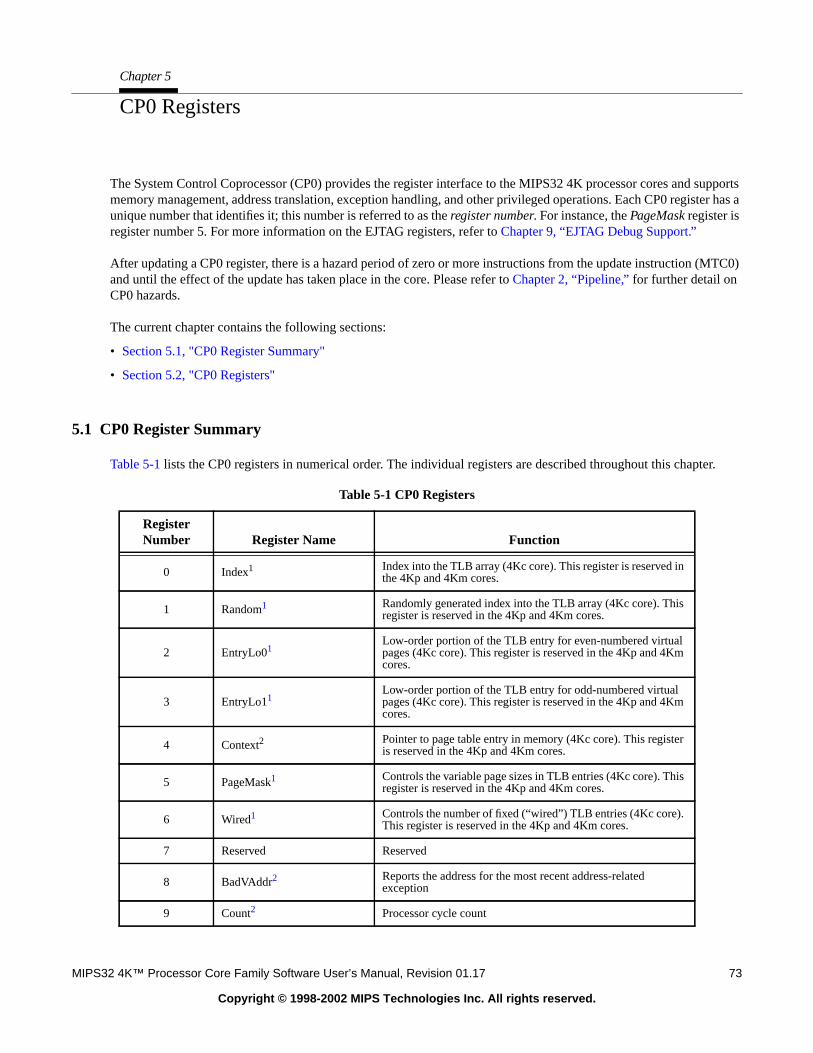
upportster has a
TC0)
ter.
Chapter 5
CP0 Registers
The System Control Coprocessor (CP0) provides the register interface to the MIPS32 4K processor cores and smemory management, address translation, exception handling, and other privileged operations. Each CP0 regisunique number that identifies it; this number is referred to as theregister number. For instance, thePageMaskregister isregister number 5. For more information on the EJTAG registers, refer toChapter 9, “EJTAG Debug Support.”
After updating a CP0 register, there is a hazard period of zero or more instructions from the update instruction (Mand until the effect of the update has taken place in the core. Please refer toChapter 2, “Pipeline,” for further detail onCP0 hazards.
The current chapter contains the following sections:
• Section 5.1, "CP0 Register Summary"
• Section 5.2, "CP0 Registers"
5.1 CP0 Register Summary
Table 5-1 lists the CP0 registers in numerical order. The individual registers are described throughout this chap
Table 5-1 CP0 Registers
RegisterNumber Register Name Function
0 Index1 Index into the TLB array (4Kc core). This register is reserved inthe 4Kp and 4Km cores.
1 Random1 Randomly generated index into the TLB array (4Kc core). Thisregister is reserved in the 4Kp and 4Km cores.
2 EntryLo01Low-order portion of the TLB entry for even-numbered virtualpages (4Kc core). This register is reserved in the 4Kp and 4Kmcores.
3 EntryLo11Low-order portion of the TLB entry for odd-numbered virtualpages (4Kc core). This register is reserved in the 4Kp and 4Kmcores.
4 Context2 Pointer to page table entry in memory (4Kc core). This registeris reserved in the 4Kp and 4Km cores.
5 PageMask1 Controls the variable page sizes in TLB entries (4Kc core). Thisregister is reserved in the 4Kp and 4Km cores.
6 Wired1 Controls the number of fixed (“wired”) TLB entries (4Kc core).This register is reserved in the 4Kp and 4Km cores.
7 Reserved Reserved
8 BadVAddr2 Reports the address for the most recent address-relatedexception
9 Count2 Processor cycle count
MIPS32 4K™ Processor Core Family Software User’s Manual, Revision 01.17 73
Copyright © 1998-2002 MIPS Technologies Inc. All rights reserved.
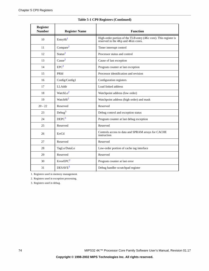
Chapter 5 CP0 Registers
10 EntryHi1 High-order portion of the TLB entry (4Kc core). This register isreserved in the 4Kp and 4Km cores.
11 Compare2 Timer interrupt control
12 Status2 Processor status and control
13 Cause2 Cause of last exception
14 EPC2 Program counter at last exception
15 PRId Processor identification and revision
16 Config/Config1 Configuration registers
17 LLAddr Load linked address
18 WatchLo2 Watchpoint address (low order)
19 WatchHi2 Watchpoint address (high order) and mask
20 - 22 Reserved Reserved
23 Debug3 Debug control and exception status
24 DEPC3 Program counter at last debug exception
25 Reserved Reserved
26 ErrCtl Controls access to data and SPRAM arrays for CACHEinstruction
27 Reserved Reserved
28 TagLo/DataLo Low-order portion of cache tag interface
29 Reserved Reserved
30 ErrorEPC2 Program counter at last error
31 DESAVE3 Debug handler scratchpad register
1. Registers used in memory management.
2. Registers used in exception processing.
3. Registers used in debug.
Table 5-1 CP0 Registers (Continued)
RegisterNumber Register Name Function
74 MIPS32 4K™ Processor Core Family Software User’s Manual, Revision 01.17
Copyright © 1998-2002 MIPS Technologies Inc. All rights reserved.

5.2 CP0 Registers
with the
t state of
5.2 CP0 Registers
The CP0 registers provide the interface between the ISA and the architecture. Each register is discussed below,registers presented in numerical order, first by register number, then by select field number.
For each register described below, field descriptions include the read/write properties of the field, and the resethe field. For the read/write properties of the field, the following notation is used:
Table 5-2 CP0 Register Field Types
Read/WriteNotation Hardware Interpretation Software Interpretation
R/W
A field in which all bits are readable and writable by software and, potentially, by hardware.
Hardware updates of this field are visible by software read. Software updates of this field arevisible by hardware read.
If the reset state of this field is “Undefined,” either software or hardware must initialize the valuebefore the first read will return a predictable value. This should not be confused with the formaldefinition of UNDEFINED behavior.
R
A field that is either static or is updated only byhardware.
If the Reset State of this field is either “0” or“Preset”, hardware initializes this field to zeroor to the appropriate state, respectively, onpowerup.
If the Reset State of this field is “Undefined”,hardware updates this field only under thoseconditions specified in the description of thefield.
A field to which the value written by softwareis ignored by hardware. Software may writeany value to this field without affectinghardware behavior. Software reads of this fieldreturn the last value updated by hardware.
If the Reset State of this field is “Undefined,”software reads of this field result in anUNPREDICTABLE value except after ahardware update done under the conditionsspecified in the description of the field.
0 A field that hardware does not update, and forwhich hardware can assume a zero value.
A field to which the value written by softwaremust be zero. Software writes of non-zerovalues to this field may result in UNDEFINEDbehavior of the hardware. Software reads ofthis field return zero as long as all previoussoftware writes are zero.
If the Reset State of this field is “Undefined,”software must write this field with zero beforeit is guaranteed to read as zero.
MIPS32 4K™ Processor Core Family Software User’s Manual, Revision 01.17 75
Copyright © 1998-2002 MIPS Technologies Inc. All rights reserved.

Chapter 5 CP0 Registers
, andB
ritten
5.2.1 Index Register (CP0 Register 0, Select 0)
TheIndex register is a 32-bit read/write register that contains the index used to access the TLB for TLBP, TLBRTLBWI instructions. The width of the index field is implementation-dependent as a function of the number of TLentries that are implemented. The minimum value for TLB-based MMUs isCeiling(Log2(TLBEntries)).
The operation of the processor is UNDEFINED if a value greater than or equal to the number of TLB entries is wto theIndex register.
This register is only valid with the TLB (4Kc core). It is reserved if the FM is implemented (4Km and 4Kp).
Index Register Format31 30 4 3 0
P 0 Index
Table 5-3 Index Register Field Descriptions
Fields
DescriptionRead/Write Reset StateName Bit(s)
P 31 Probe Failure. Set to 1 when the previous TLBProbe(TLBP) instruction failed to find a match in the TLB. R Undefined
0 30:4 Must be written as zero; returns zero on read. 0 0
Index 3:0 Index to the TLB entry affected by the TLBRead andTLBWrite instructions. R/W Undefined
76 MIPS32 4K™ Processor Core Family Software User’s Manual, Revision 01.17
Copyright © 1998-2002 MIPS Technologies Inc. All rights reserved.
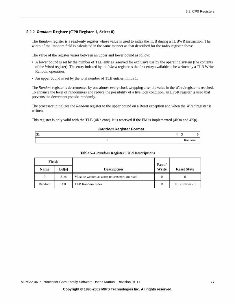
5.2 CP0 Registers
The
ontents
d that
5.2.2 Random Register (CP0 Register 1, Select 0)
TheRandom register is a read-only register whose value is used to index the TLB during a TLBWR instruction. width of the Random field is calculated in the same manner as that described for theIndex register above.
The value of the register varies between an upper and lower bound as follow:
• A lower bound is set by the number of TLB entries reserved for exclusive use by the operating system (the cof theWiredregister). The entry indexed by theWiredregister is the first entry available to be written by a TLB WriteRandom operation.
• An upper bound is set by the total number of TLB entries minus 1.
TheRandomregister is decremented by one almost every clock wrapping after the value in theWiredregister is reached.To enhance the level of randomness and reduce the possibility of a live lock condition, an LFSR register is useprevents the decrement pseudo-randomly.
The processor initializes theRandom register to the upper bound on a Reset exception and when theWired register iswritten.
This register is only valid with the TLB (4Kc core). It is reserved if the FM is implemented (4Km and 4Kp).
Random Register Format31 4 3 0
0 Random
Table 5-4Random Register Field Descriptions
Fields
DescriptionRead/Write Reset StateName Bit(s)
0 31:4 Must be written as zero; returns zero on read. 0 0
Random 3:0 TLB Random Index R TLB Entries - 1
MIPS32 4K™ Processor Core Family Software User’s Manual, Revision 01.17 77
Copyright © 1998-2002 MIPS Technologies Inc. All rights reserved.

Chapter 5 CP0 Registers
ns.
ed,
4Kp).
5.2.3 EntryLo0, EntryLo1 (CP0 Registers 2 and 3, Select 0)
The pair ofEntryLo registers act as the interface between the TLB and the TLBR, TLBWI, and TLBWR instructioFor a TLB-based MMU,EntryLo0 holds the entries for even pages andEntryLo1 holds the entries for odd pages.
The contents of theEntryLo0 andEntryLo1 registers are undefined after an address error, TLB invalid, TLB modifior TLB refill exceptions.
These registers are only valid with the TLB (4Kc core). They are reserved if the FM is implemented (4Km and
EntryLo0 , EntryLo1 Register Format
Table 5-6lists the encoding of the C field of theEntryLo0andEntryLo1registers and the K0 field of theConfigregister.
31 30 29 26 25 6 5 3 2 1 0
R 0 PFN C D V G
Table 5-5EntryLo0, EntryLo1 Register Field Descriptions
Fields
DescriptionRead/Write Reset StateName Bit(s)
R 31:30 Reserved. Should be ignored on writes; returns zero on read. R 0
0 29:26
These 4 bits are normally part of the PFN. However, since thecore supports only 32-bits of physical address, the PFN is only20-bits wide. Therefore, bits 29:26 of this register must bewritten with zeros.
R/W 0
PFN 25:6 Page Frame Number. Corresponds to bits 31:12 of thephysical address. R/W Undefined
C 5:3 Coherency attribute of the page. SeeTable 5-6. R/W Undefined
D 2
“Dirty” or write-enable bit, indicating that the page has beenwritten, and/or is writable. If this bit is a one, stores to the pageare permitted. If this bit is a zero, stores to the page cause aTLB Modified exception.
R/W Undefined
V 1
Valid bit, indicating that the TLB entry, and thus the virtualpage mapping are valid. If this bit is a one, accesses to the pageare permitted. If this bit is a zero, accesses to the page cause aTLB Invalid exception.
R/W Undefined
G 0
Global bit. On a TLB write, the logical AND of the G bits inboth the EntryLo0 and EntryLo1 registers become the G bit inthe TLB entry. If the TLB entry G bit is a one, ASIDcomparisons are ignored during TLB matches. On a read froma TLB entry, the G bits of both EntryLo0 and EntryLo1 reflectthe state of the TLB G bit.
R/W Undefined
Table 5-6 Cache Coherency Attributes
C(5:3) Value Cache Coherency Attribute
0, 1, 3*, 4, 5, 6 Cacheable, noncoherent, write through, no write allocate
2*, 7 Uncached
78 MIPS32 4K™ Processor Core Family Software User’s Manual, Revision 01.17
Copyright © 1998-2002 MIPS Technologies Inc. All rights reserved.

5.2 CP0 Registers
Note: * These two values are required by the MIPS32 architecture. All other values are not used. For example, values 0, 1, 4, 5 and6 are not used and are mapped to 3. The value 7 is not used and is mapped to 2. Note that these values do have meaning in otherMIPS Technologies processor implementations. Refer to the MIPS32 specification for more information.
Table 5-6 Cache Coherency Attributes
C(5:3) Value Cache Coherency Attribute
MIPS32 4K™ Processor Core Family Software User’s Manual, Revision 01.17 79
Copyright © 1998-2002 MIPS Technologies Inc. All rights reserved.
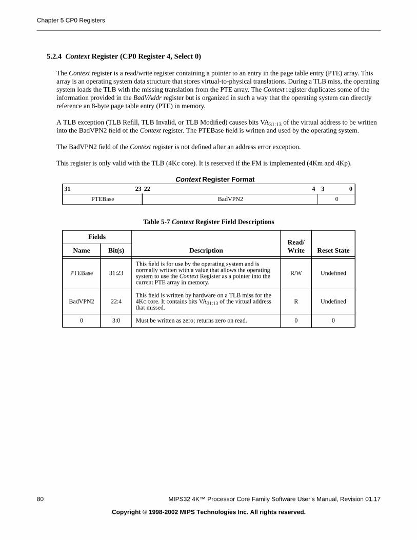
Chapter 5 CP0 Registers
Thiserating
tly
5.2.4 Context Register (CP0 Register 4, Select 0)
TheContext register is a read/write register containing a pointer to an entry in the page table entry (PTE) array.array is an operating system data structure that stores virtual-to-physical translations. During a TLB miss, the opsystem loads the TLB with the missing translation from the PTE array. TheContext register duplicates some of theinformation provided in theBadVAddr register but is organized in such a way that the operating system can direcreference an 8-byte page table entry (PTE) in memory.
A TLB exception (TLB Refill, TLB Invalid, or TLB Modified) causes bits VA31:13 of the virtual address to be writteninto the BadVPN2 field of theContext register. The PTEBase field is written and used by the operating system.
The BadVPN2 field of theContext register is not defined after an address error exception.
This register is only valid with the TLB (4Kc core). It is reserved if the FM is implemented (4Km and 4Kp).
Context Register Format31 23 22 4 3 0
PTEBase BadVPN2 0
Table 5-7Context Register Field Descriptions
Fields
DescriptionRead/Write Reset StateName Bit(s)
PTEBase 31:23
This field is for use by the operating system and isnormally written with a value that allows the operatingsystem to use theContext Register as a pointer into thecurrent PTE array in memory.
R/W Undefined
BadVPN2 22:4This field is written by hardware on a TLB miss for the4Kc core. It contains bits VA31:13 of the virtual addressthat missed.
R Undefined
0 3:0 Must be written as zero; returns zero on read. 0 0
80 MIPS32 4K™ Processor Core Family Software User’s Manual, Revision 01.17
Copyright © 1998-2002 MIPS Technologies Inc. All rights reserved.

5.2 CP0 Registers
ask
5.2.5 PageMask Register (CP0 Register 5, Select 0)
ThePageMaskregister is a read/write register used for reading from and writing to the TLB. It holds a comparison mthat sets the variable page size for each TLB entry as shown inTable 5-9. Behavior isUNDEFINED if a value otherthan those listed is used.
This register is only valid with the TLB (4Kc core). It is reserved if the FM is implemented (4Km and 4Kp).
PageMask Register Format31 25 24 13 12 0
0 Mask 0
Table 5-8PageMask Register Field Descriptions
Fields
DescriptionRead/Write Reset StateName Bit(s)
Mask 24:13The Mask field is a bit mask in which a “1” indicates thatthe corresponding bit of the virtual address should notparticipate in the TLB match.
R/W Undefined
0 31:25,12:0 Must be written as zero; returns zero on read. 0 0
Table 5-9 Values for the Mask Field of thePageMask Register
Page Size
Bit
24 23 22 21 20 19 18 17 16 15 14 13
4 KBytes 0 0 0 0 0 0 0 0 0 0 0 0
16 KBytes 0 0 0 0 0 0 0 0 0 0 1 1
64 KBytes 0 0 0 0 0 0 0 0 1 1 1 1
256 KBytes 0 0 0 0 0 0 1 1 1 1 1 1
1 MByte 0 0 0 0 1 1 1 1 1 1 1 1
4 MByte 0 0 1 1 1 1 1 1 1 1 1 1
16 Mbyte 1 1 1 1 1 1 1 1 1 1 1 1
MIPS32 4K™ Processor Core Family Software User’s Manual, Revision 01.17 81
Copyright © 1998-2002 MIPS Technologies Inc. All rights reserved.

Chapter 5 CP0 Registers
e TLB
Wired
to the
5.2.6 Wired Register (CP0 Register 6, Select 0)
TheWiredregister is a read/write register that specifies the boundary between the wired and random entries in thas shown inFigure 5-1. The width of the Wired field is calculated in the same manner as that described for theIndexregister above. Wired entries are fixed, non-replaceable entries that are not overwritten by a TLBWR instruction.entries can be overwritten by a TLBWI instruction.
TheWiredregister is set to zero by a Reset exception. Writing theWiredregister causes theRandomregister to reset toits upper bound.
The operation of the processor is undefined if a value greater than or equal to the number of TLB entries is writtenWired register.
This register is only valid with a TLB (4Kc core). It is reserved if the FM is implemented (4Km and 4Kp cores).
Figure 5-1 Wired and Random Entries in the TLB
Wired Register Format31 4 3 0
0 Wired
Table 5-10 Wired Register Field Descriptions
Fields
DescriptionRead/Write Reset StateName Bit(s)
0 31:4 Must be written as zero; returns zero on read. 0 0
Wired 3:0 TLB wired boundary. R/W 0
Entry 0
Entry 10
Entry n-1
10Wired Register
Wire
dR
ando
m
82 MIPS32 4K™ Processor Core Family Software User’s Manual, Revision 01.17
Copyright © 1998-2002 MIPS Technologies Inc. All rights reserved.

5.2 CP0 Registers
he
g error.
5.2.7 BadVAddr Register (CP0 Register 8, Select 0)
TheBadVAddr register is a read-only register that captures the most recent virtual address that caused one of tfollowing exceptions:
• Address error (AdEL or AdES)
• TLB Refill (4Kc core)
• TLB Invalid (4Kc core)
• TLB Modified (4Kc core)
TheBadVAddrregister does not capture address information for cache or bus errors, since neither is an addressin
BadVAddr Register Format31 0
BadVAddr
Table 5-11BadVAddr Register Field Description
Fields
DescriptionRead/Write Reset StateName Bits
BadVAddr 31:0 Bad virtual address R Undefined
MIPS32 4K™ Processor Core Family Software User’s Manual, Revision 01.17 83
Copyright © 1998-2002 MIPS Technologies Inc. All rights reserved.

Chapter 5 CP0 Registers
ired, or
ssors.
ntDM
5.2.8 Count Register (CP0 Register 9, Select 0)
TheCountregister acts as a timer, incrementing at a constant rate, whether or not an instruction is executed, retany forward progress is made through the pipeline. The counter increments every other clock.
TheCountregister can be written for functional or diagnostic purposes, including at reset or to synchronize proce
Whether theCountregister continues incrementing while the processor is in debug mode is determined by the Coubit in theDebug register (seeSection 5.2.20, "Debug Register (CP0 Register 23)" on page 102).
Count Register Format31 0
Count
Table 5-12Count Register Field Description
Fields
DescriptionRead/Write Reset StateName Bits
Count 31:0 Interval counter. R/W Undefined
84 MIPS32 4K™ Processor Core Family Software User’s Manual, Revision 01.17
Copyright © 1998-2002 MIPS Technologies Inc. All rights reserved.
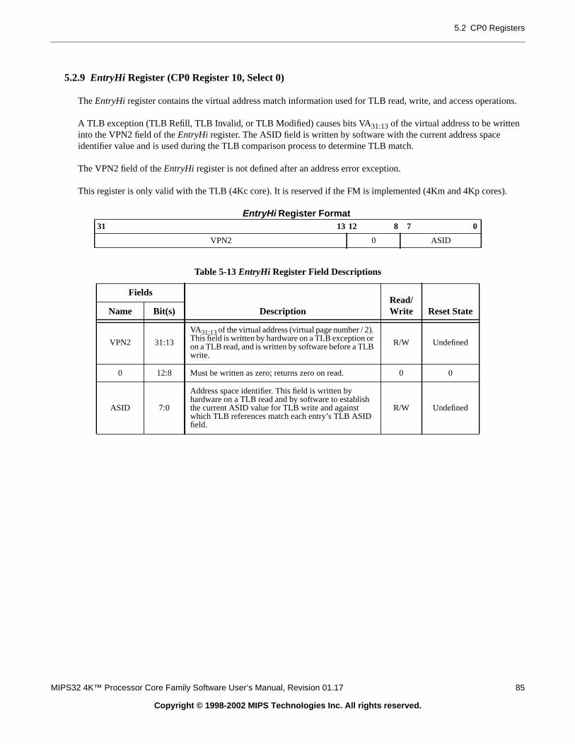
5.2 CP0 Registers
tions.
).
5.2.9 EntryHi Register (CP0 Register 10, Select 0)
TheEntryHi register contains the virtual address match information used for TLB read, write, and access opera
A TLB exception (TLB Refill, TLB Invalid, or TLB Modified) causes bits VA31:13 of the virtual address to be writteninto the VPN2 field of theEntryHi register. The ASID field is written by software with the current address spaceidentifier value and is used during the TLB comparison process to determine TLB match.
The VPN2 field of theEntryHi register is not defined after an address error exception.
This register is only valid with the TLB (4Kc core). It is reserved if the FM is implemented (4Km and 4Kp cores
EntryHi Register Format31 13 12 8 7 0
VPN2 0 ASID
Table 5-13EntryHi Register Field Descriptions
Fields
DescriptionRead/Write Reset StateName Bit(s)
VPN2 31:13
VA31:13of the virtual address (virtual page number / 2).This field is written by hardware on a TLB exception oron a TLB read, and is written by software before a TLBwrite.
R/W Undefined
0 12:8 Must be written as zero; returns zero on read. 0 0
ASID 7:0
Address space identifier. This field is written byhardware on a TLB read and by software to establishthe current ASID value for TLB write and againstwhich TLB references match each entry’s TLB ASIDfield.
R/W Undefined
MIPS32 4K™ Processor Core Family Software User’s Manual, Revision 01.17 85
Copyright © 1998-2002 MIPS Technologies Inc. All rights reserved.

Chapter 5 CP0 Registers
ewn.
ofrupt 5
5.2.10 Compare Register (CP0 Register 11, Select 0)
TheCompareregister acts in conjunction with theCountregister to implement a timer and timer interrupt function. Thtimer interrupt is an output of the cores. TheCompareregister maintains a stable value and does not change on its o
When the value of theCountregister equals the value of theCompareregister, the SI_TimerInt pin is asserted. This pinwill remain asserted until theCompareregister is written. The SI_TimerInt pin can be fed back into the core on onethe interrupt pins to generate an interrupt. Traditionally, this has been done by multiplexing it with hardware interto set interrupt bit IP(7) in theCause register.
For diagnostic purposes, theCompare register is a read/write register. In normal use, however, theCompare register iswrite-only. Writing a value to theCompare register, as a side effect, clears the timer interrupt.
Compare Register Format31 0
Compare
Table 5-14Compare Register Field Description
Fields
DescriptionRead/Write Reset StateName Bit(s)
Compare 31:0 Interval count compare value R/W Undefined
86 MIPS32 4K™ Processor Core Family Software User’s Manual, Revision 01.17
Copyright © 1998-2002 MIPS Technologies Inc. All rights reserved.

5.2 CP0 Registers
nostic:
sor is
ble,
5.2.11 Status Register (CP0 Register 12, Select 0)
TheStatusregister (SR) is a read/write register that contains the operating mode, interrupt enabling, and the diagstates of the processor. Fields of this register combine to create operating modes for the processor, as follows
Interrupt Enable : Interrupts are enabled when all of the following conditions are true:
• IE = 1
• EXL = 0
• ERL = 0
• DM = 0
If these conditions are met, the settings of the IM and IE bits enable the interrupt.
Operating Modes: If the DM bit in the Debug register is 1, the processor is in debug mode. Otherwise the procesin either kernel or user mode. The following CPU Status register bit settings determine user or kernel mode.
• User mode: UM = 1, EXL = 0, and ERL = 0
• Kernel mode: UM = 0, or EXL = 1, or ERL = 1
Coprocessor Accessibility:TheStatusregister CU bits control coprocessor accessibility. If any coprocessor is unusaan instruction that accesses it generates an exception.
Coprocessor 0 is always enabled in kernel mode, regardless of the setting of the CU0 bit.
MIPS32 4K™ Processor Core Family Software User’s Manual, Revision 01.17 87
Copyright © 1998-2002 MIPS Technologies Inc. All rights reserved.

Chapter 5 CP0 Registers
Status Register Format31 28 27 26 25 24 23 22 21 20 19 18 17 16 15 8 7 5 4 3 2 1 0
CU3-CU0 RP R RE 0 BEV TS SR NMI 0 0 IM7-IM0 R UM R ERL EXL IE
Table 5-15Status Register Field Descriptions
Fields
DescriptionRead/Write Reset StateName Bit(s)
CU3-CU0 31:28
Controls access to coprocessors 3, 2, 1, and 0,respectively:
0: access not allowed1: access allowed
Coprocessor 0 is always usable when the processor isrunning in kernel mode, independent of the state of theCU0 bit.
The core does not support coprocessors 1-3, but CU3:1can still be set. However, processor behavior isunpredictable if a coprocessor instruction tocoprocessors 1-3 is attempted with the correspondingCU3:1 bit set.
R/W Undefined
RP 27 Enables reduced power mode. The state of the RP bit isavailable on the bus interface as the SI_RP signal. R/W 0 for Cold
Reset only.
R 26 This bit must be ignored on writes and read as zero. R 0
RE 25
Used to enable reverse-endian memory referenceswhile the processor is running in user mode:
0: User mode uses configured endianness1: User mode uses reversed endianness
Kernel or debug mode references are not affected bythe state of this bit.
R/W Undefined
0 24:23 This bit must be written as zero; returns zero on read. R 0
BEV 22
Controls the location of exception vectors:
0: Normal1: Bootstrap
R/W 1
TS 21
TLB shutdown. This bit is set if a TLBWI or TLBWRinstruction is issued that would cause a TLB shutdowncondition if allowed to complete. This bit is only usedin the 4Kc processor and is reserved in the 4Kp and4Km processors.
Software can only write a 0 to this bit to clear it andcannot force a 0-1 transition.
R/W 0
SR 20
Indicates that the entry through the reset exceptionvector was due to a Soft Reset:
0: Not Soft Reset (NMI or hard reset)1: Soft Reset
Software can only write a 0 to this bit to clear it andcannot force a 0-1 transition.
R/W1 for SoftReset; 0
otherwise
88 MIPS32 4K™ Processor Core Family Software User’s Manual, Revision 01.17
Copyright © 1998-2002 MIPS Technologies Inc. All rights reserved.
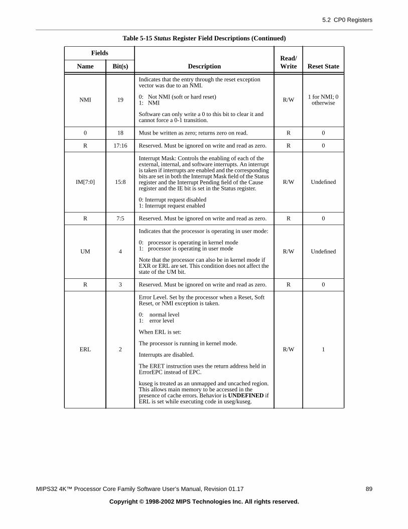
5.2 CP0 Registers
NMI 19
Indicates that the entry through the reset exceptionvector was due to an NMI.
0: Not NMI (soft or hard reset)1: NMI
Software can only write a 0 to this bit to clear it andcannot force a 0-1 transition.
R/W 1 for NMI; 0otherwise
0 18 Must be written as zero; returns zero on read. R 0
R 17:16 Reserved. Must be ignored on write and read as zero. R 0
IM[7:0] 15:8
Interrupt Mask: Controls the enabling of each of theexternal, internal, and software interrupts. An interruptis taken if interrupts are enabled and the correspondingbits are set in both the Interrupt Mask field of the Statusregister and the Interrupt Pending field of the Causeregister and the IE bit is set in the Status register.
0: Interrupt request disabled1: Interrupt request enabled
R/W Undefined
R 7:5 Reserved. Must be ignored on write and read as zero. R 0
UM 4
Indicates that the processor is operating in user mode:
0: processor is operating in kernel mode1: processor is operating in user mode
Note that the processor can also be in kernel mode ifEXR or ERL are set. This condition does not affect thestate of the UM bit.
R/W Undefined
R 3 Reserved. Must be ignored on write and read as zero. R 0
ERL 2
Error Level. Set by the processor when a Reset, SoftReset, or NMI exception is taken.
0: normal level1: error level
When ERL is set:
The processor is running in kernel mode.
Interrupts are disabled.
The ERET instruction uses the return address held inErrorEPC instead of EPC.
kuseg is treated as an unmapped and uncached region.This allows main memory to be accessed in thepresence of cache errors. Behavior isUNDEFINED ifERL is set while executing code in useg/kuseg.
R/W 1
Table 5-15Status Register Field Descriptions (Continued)
Fields
DescriptionRead/Write Reset StateName Bit(s)
MIPS32 4K™ Processor Core Family Software User’s Manual, Revision 01.17 89
Copyright © 1998-2002 MIPS Technologies Inc. All rights reserved.
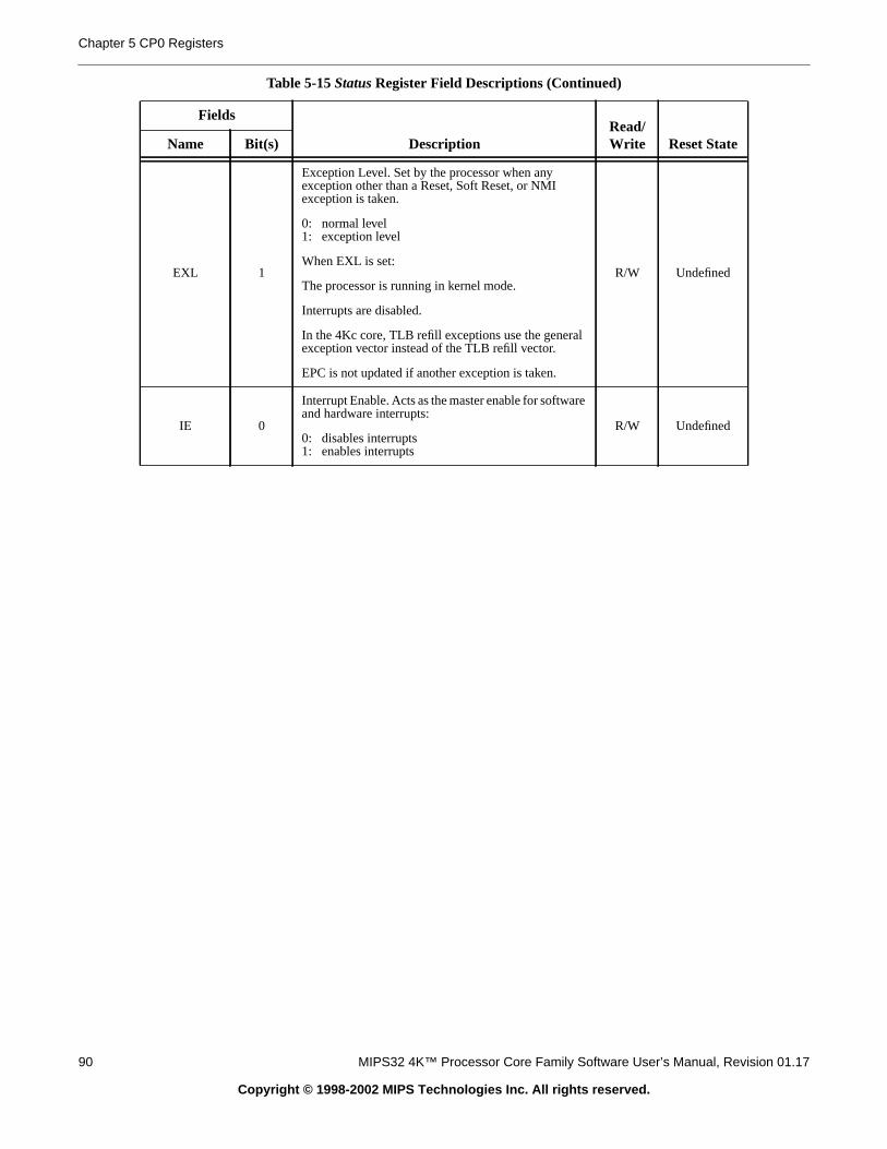
Chapter 5 CP0 Registers
EXL 1
Exception Level. Set by the processor when anyexception other than a Reset, Soft Reset, or NMIexception is taken.
0: normal level1: exception level
When EXL is set:
The processor is running in kernel mode.
Interrupts are disabled.
In the 4Kc core, TLB refill exceptions use the generalexception vector instead of the TLB refill vector.
EPC is not updated if another exception is taken.
R/W Undefined
IE 0
Interrupt Enable. Acts as the master enable for softwareand hardware interrupts:
0: disables interrupts1: enables interrupts
R/W Undefined
Table 5-15Status Register Field Descriptions (Continued)
Fields
DescriptionRead/Write Reset StateName Bit(s)
90 MIPS32 4K™ Processor Core Family Software User’s Manual, Revision 01.17
Copyright © 1998-2002 MIPS Technologies Inc. All rights reserved.

5.2 CP0 Registers
ftwared WP
5.2.12 Cause Register (CP0 Register 13, Select 0)
TheCause register primarily describes the cause of the most recent exception. In addition, fields also control sointerrupt requests and the vector through which interrupts are dispatched. With the exception of the IP[1:0], IV, anfields, all fields in the Cause register are read-only.
Cause Register Format31 30 29 28 27 24 23 22 21 16 15 10 9 8 7 6 5 4 3 2 1 0
BD 0 CE 0 IV WP 0 IP[7:2] IP[1:0] 0 Exc Code 0
Table 5-16Cause Register Field Descriptions
Fields
DescriptionRead/Write Reset StateName Bit(s)
BD 31
Indicates whether the last exception taken occurred in a branchdelay slot:
0: Not in delay slot1: In delay slot
Note that the BD bit is not updated on a new exception if theEXL bit is set.
R Undefined
CE 29:28
Coprocessor unit number referenced when a CoprocessorUnusable exception is taken. This field is loaded by hardwareon every exception but is unpredictable for all exceptionsexcept for Coprocessor Unusable.
R Undefined
IV 23
Indicates whether an interrupt exception uses the generalexception vector or a special interrupt vector:
0: Use the general exception vector (0x180)1: Use the special interrupt vector (0x200)
R/W Undefined
WP 22
Indicates that a watch exception was deferred becauseStatusEXL or StatusERL were a one at the time the watchexception was detected. This bit both indicates that the watchexception was deferred and causes the exception to be initiatedonceStatusEXL andStatusERL are both zero. As such, softwaremust clear this bit as part of the watch exception handler toprevent a watch exception loop.
Software can only write a 0 to this bit to clear it and cannotforce a 0-1 transition.
R/W Undefined
IP[7:2] 15:10
Indicates an external interrupt is pending:
15: Hardware interrupt 5 or timer interrupt14: Hardware interrupt 413: Hardware interrupt 312: Hardware interrupt 211: Hardware interrupt 110: Hardware interrupt 0
R Undefined
IP[1:0] 9:8
Controls the request for software interrupts:
9: Request software interrupt 18: Request software interrupt 0
R/W Undefined
Exc Code 6:2 Exception code — seeTable 5-17. R Undefined
MIPS32 4K™ Processor Core Family Software User’s Manual, Revision 01.17 91
Copyright © 1998-2002 MIPS Technologies Inc. All rights reserved.

Chapter 5 CP0 Registers
0
30,27:24,
21:16, 7,1:0
Must be written as zero; returns zero on read. R 0
Table 5-17 Cause Register ExcCode Field Descriptions
ExceptionCode Value Mnemonic Description
0 Int Interrupt
1 Mod TLB modification exception (4Kc core) or Reserved (4Km and 4Kp cores)
2 TLBL TLB exception (load or instruction fetch) (4Kc core) or Reserved (4Km and 4Kp cores)
3 TLBS TLB exception (store) (4Kc core) or Reserved (4Km and 4Kp cores)
4 AdEL Address error exception (load or instruction fetch)
5 AdES Address error exception (store)
6 IBE Bus error exception (instruction fetch)
7 DBE Bus error exception (data reference: load or store)
8 Sys Syscall exception
9 Bp Breakpoint exception
10 RI Reserved instruction exception
11 CpU Coprocessor Unusable exception
12 Ov Integer Overflow exception
13 Tr Trap exception
14-22 - Reserved
23 WATCH Reference to WatchHi/WatchLo address
24 MCheck Machine check (4Kc core) or Reserved (4Km and 4Kp cores)
25-31 - Reserved
Table 5-16Cause Register Field Descriptions (Continued)
Fields
DescriptionRead/Write Reset StateName Bit(s)
92 MIPS32 4K™ Processor Core Family Software User’s Manual, Revision 01.17
Copyright © 1998-2002 MIPS Technologies Inc. All rights reserved.
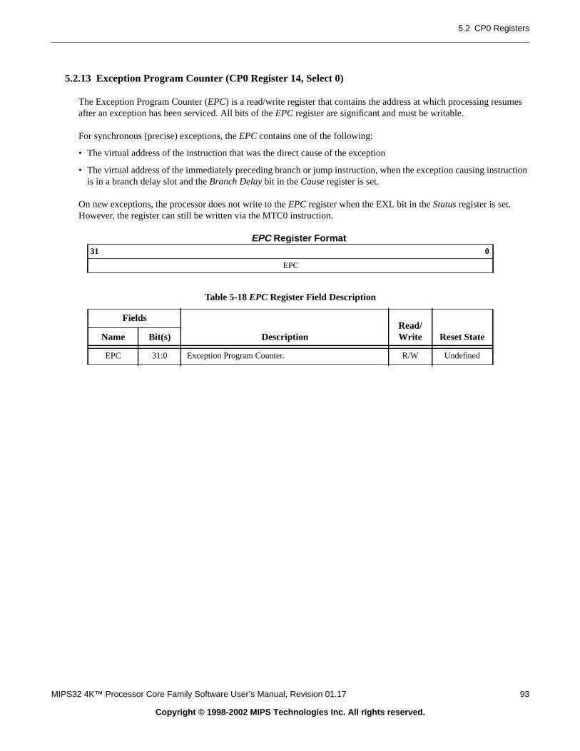
5.2 CP0 Registers
mes
uction
5.2.13 Exception Program Counter (CP0 Register 14, Select 0)
The Exception Program Counter (EPC) is a read/write register that contains the address at which processing resuafter an exception has been serviced. All bits of theEPC register are significant and must be writable.
For synchronous (precise) exceptions, theEPC contains one of the following:
• The virtual address of the instruction that was the direct cause of the exception
• The virtual address of the immediately preceding branch or jump instruction, when the exception causing instris in a branch delay slot and theBranch Delay bit in theCause register is set.
On new exceptions, the processor does not write to theEPC register when the EXL bit in theStatus register is set.However, the register can still be written via the MTC0 instruction.
EPC Register Format31 0
EPC
Table 5-18EPC Register Field Description
Fields
DescriptionRead/Write Reset StateName Bit(s)
EPC 31:0 Exception Program Counter. R/W Undefined
MIPS32 4K™ Processor Core Family Software User’s Manual, Revision 01.17 93
Copyright © 1998-2002 MIPS Technologies Inc. All rights reserved.

Chapter 5 CP0 Registers
5.2.14 Processor Identification (CP0 Register 15, Select 0)
The Processor Identification (PRId) register is a 32-bit read-only register that contains information identifying themanufacturer, manufacturer options, processor identification, and revision level of the processor.
PRId Register Format31 24 23 16 15 8 7 0
R Company ID Processor ID Revision
Table 5-19PRId Register Field Descriptions
Fields
DescriptionRead/Write Reset StateName Bit(s)
R 31:24 Reserved. Must be ignored on write and read as zero R 0
CompanyID 23:16
Identifies the company that designed or manufactured theprocessor. In all three cores this field contains a value of1 to indicate MIPS Technologies, Inc.
R 1
ProcessorID 15:8
Identifies the type of processor. This field allows softwareto distinguish between the various types of MIPSTechnologies processors. This field contains a value of0x80 for the 4Kc processor. The value is 0x83 for the 4Kpand 4Km processors.
R
4Kccore - 0x80
4Km & 4Kpcores - 0x83
Revision 7:0
Specifies the revision number of the processor. This fieldallows software to distinguish between one revision andanother of the same processor type. Current values:
0x1: 1.1-2.20x2: 2.3-2.40x3: 2.5-2.60x4: 3.00x5: 3.10x6: 3.20x7: 3.30x8: 3.40x9: 3.50xa: 3.60xb: 3.7
R Preset
94 MIPS32 4K™ Processor Core Family Software User’s Manual, Revision 01.17
Copyright © 1998-2002 MIPS Technologies Inc. All rights reserved.

5.2 CP0 Registers
ed by
5.2.15 Config Register (CP0 Register 16, Select 0)
TheConfigregister specifies various configuration and capabilities information. Most of the fields in theConfigregisterare initialized by hardware during the Reset exception process, or are constant. One field, K0, must be initializsoftware in the Reset exception handler.
Config Register Format — Select 031 30 28 27 25 24 23 22 21 20 19 18 17 16 15 14 13 12 10 9 7 6 3 2 0
M K23 KU ISP DSP 0 SB MDU R MM BM BE AT AR MT 0 K0
Table 5-20Config Register Field Descriptions
Fields
DescriptionRead/Write Reset StateName Bit(s)
M 31 This bit is hardwired to ‘1’ to indicate the presence of theConfig1 register. R 1
K23 30:28
This field controls the cacheability of the kseg2 and kseg3address segments in FM implementations. This field isvalid in the 4Kp and 4Km processor and is reserved in the4Kc processor (must be written as 0; returns 0 on read).
Refer toTable 5-21 for the field encoding.
FM: R/W
TLB: 0
FM: 010
TLB: 000
KU 27:25
This field controls the cacheability of the kuseg and usegaddress segments in FM implementations. This field isvalid in the 4Kp and 4Km processor and is reserved in the4Kc processor (must be written as 0; returns 0 on read).
Refer toTable 5-21 for the field encoding.
FM: R/W
TLB: 0
FM: 010
TLB: 000
ISP 24 This field indicates the presence of an I-side scratchpadRAM R Preset
DSP 23 This field indicates the presence of a D-side scratchpadRAM R Preset
0 22 Must be written as 0. Returns 0 on read. 0 0
SB 21
Indicates whether SimpleBE bus mode is enabled. Set viaSI_SimpleBE[0] input pin
0 = No reserved byte enables on EC interface1 = Only simple byte enables allowed on EC interface
R Externally Set
MDU 20
This bit indicates the MDU type.
0 = Fast Multiplier Array (4Kc and 4Km cores)1 = Iterative multiplier (4Kp cores)
R Preset
0 19 Must be written as 0. Returns 0 on read. 0 0
MM 18:17
This field contains the merge mode for the 32-bytecollapsing write buffer:
00 = No Merging01 = SysAD Valid merging10 = Full merging11 = Reserved
R Externally Set
MIPS32 4K™ Processor Core Family Software User’s Manual, Revision 01.17 95
Copyright © 1998-2002 MIPS Technologies Inc. All rights reserved.
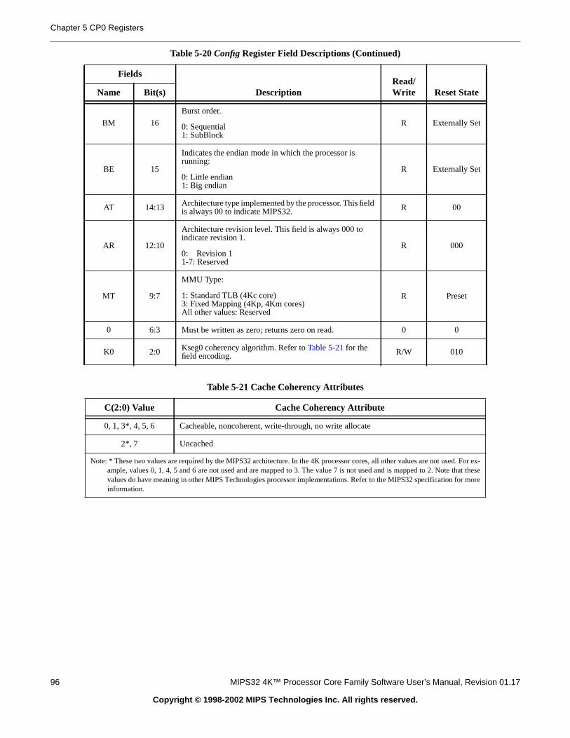
Chapter 5 CP0 Registers
BM 16
Burst order.
0: Sequential1: SubBlock
R Externally Set
BE 15
Indicates the endian mode in which the processor isrunning:
0: Little endian1: Big endian
R Externally Set
AT 14:13 Architecture type implemented by the processor. This fieldis always 00 to indicate MIPS32. R 00
AR 12:10
Architecture revision level. This field is always 000 toindicate revision 1.
0: Revision 11-7: Reserved
R 000
MT 9:7
MMU Type:
1: Standard TLB (4Kc core)3: Fixed Mapping (4Kp, 4Km cores)All other values: Reserved
R Preset
0 6:3 Must be written as zero; returns zero on read. 0 0
K0 2:0 Kseg0 coherency algorithm. Refer toTable 5-21 for thefield encoding. R/W 010
Table 5-21 Cache Coherency Attributes
C(2:0) Value Cache Coherency Attribute
0, 1, 3*, 4, 5, 6 Cacheable, noncoherent, write-through, no write allocate
2*, 7 Uncached
Note: * These two values are required by the MIPS32 architecture. In the 4K processor cores, all other values are not used. For ex-ample, values 0, 1, 4, 5 and 6 are not used and are mapped to 3. The value 7 is not used and is mapped to 2. Note that thesevalues do have meaning in other MIPS Technologies processor implementations. Refer to the MIPS32 specification for moreinformation.
Table 5-20Config Register Field Descriptions (Continued)
Fields
DescriptionRead/Write Reset StateName Bit(s)
96 MIPS32 4K™ Processor Core Family Software User’s Manual, Revision 01.17
Copyright © 1998-2002 MIPS Technologies Inc. All rights reserved.

5.2 CP0 Registers
MIPS32 4K™ Processor Core Family Software User’s Manual, Revision 01.17 97
Copyright © 1998-2002 MIPS Technologies Inc. All rights reserved.
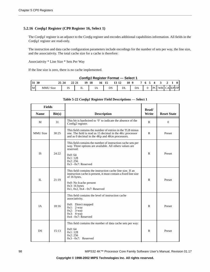
Chapter 5 CP0 Registers
e
ine size,
5.2.16 Config1 Register (CP0 Register 16, Select 1)
TheConfig1register is an adjunct to theConfigregister and encodes additional capabilities information. All fields in thConfig1 register are read-only.
The instruction and data cache configuration parameters include encodings for the number of sets per way, the land the associativity. The total cache size for a cache is therefore:
Associativity * Line Size * Sets Per Way
If the line size is zero, there is no cache implemented.
Config1 Register Format — Select 131 30 25 24 22 21 19 18 16 15 13 12 10 9 7 6 5 4 3 2 1 0
M MMU Size IS IL IA DS DL DA 0 PC WR CA EP FP
Table 5-22Config1 Register Field Descriptions — Select 1
Fields
DescriptionRead/Write Reset StateName Bit(s)
M 31 This bit is hardwired to ‘0’ to indicate the absence of theConfig2 register. R 0
MMU Size 30:25This field contains the number of entries in the TLB minusone. The field is read as 15 decimal in the 4Kc processorand as 0 decimal in the 4Kp and 4Km processors.
R Preset
IS 24:22
This field contains the number of instruction cache sets perway. Three options are available. All others values arereserved:
0x0: 640x1: 1280x2: 2560x3 - 0x7: Reserved
R Preset
IL 21:19
This field contains the instruction cache line size. If aninstruction cache is present, it must contain a fixed line sizeof 16 bytes.
0x0: No Icache present0x3: 16 bytes0x1, 0x2, 0x4 - 0x7: Reserved
R Preset
IA 18:16
This field contains the level of instruction cacheassociativity.
0x0: Direct mapped0x1: 2-way0x2: 3-way0x3: 4-way0x4 - 0x7: Reserved
R Preset
DS 15:13
This field contains the number of data cache sets per way:
0x0: 640x1: 1280x2: 2560x3 - 0x7: Reserved
R Preset
98 MIPS32 4K™ Processor Core Family Software User’s Manual, Revision 01.17
Copyright © 1998-2002 MIPS Technologies Inc. All rights reserved.
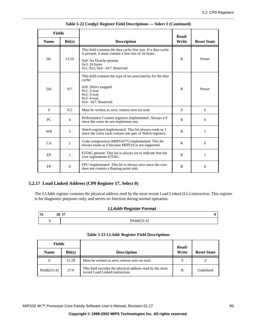
5.2 CP0 Registers
gister
5.2.17 Load Linked Address (CP0 Register 17, Select 0)
TheLLAddr register contains the physical address read by the most recent Load Linked (LL) instruction. This reis for diagnostic purposes only, and serves no function during normal operation.
LLAddr Register Format
DL 12:10
This field contains the data cache line size. If a data cacheis present, it must contain a line size of 16 bytes.
0x0: No Dcache present0x3: 16 bytes0x1, 0x2, 0x4 - 0x7: Reserved
R Preset
DA 9:7
This field contains the type of set associativity for the datacache:
0x0: Direct mapped0x1: 2-way0x2: 3-way0x3: 4-way0x4 - 0x7: Reserved
R Preset
0 6:5 Must be written as zero; returns zero on read. 0 0
PC 4 Performance Counter registers implemented. Always a 0since the cores do not implement any. R 0
WR 3 Watch registers implemented. This bit always reads as 1since the cores each contain one pair of Watch registers. R 1
CA 2 Code compression (MIPS16™) implemented. This bitalways reads as 0 because MIPS16 is not supported. R 0
EP 1 EJTAG present: This bit is always set to indicate that thecore implements EJTAG. R 1
FP 0 FPU implemented. This bit is always zero since the coredoes not contain a floating-point unit. R 0
31 28 27 0
0 PAddr[31:4]
Table 5-23LLAddr Register Field Descriptions
Fields
DescriptionRead/Write Reset StateName Bit(s)
0 31:28 Must be written as zero; returns zero on read. 0 0
PAddr[31:4] 27:0 This field encodes the physical address read by the mostrecent Load Linked instruction. R Undefined
Table 5-22Config1 Register Field Descriptions — Select 1 (Continued)
Fields
DescriptionRead/Write Reset StateName Bit(s)
MIPS32 4K™ Processor Core Family Software User’s Manual, Revision 01.17 99
Copyright © 1998-2002 MIPS Technologies Inc. All rights reserved.

Chapter 5 CP0 Registers
atchte some
e
match.
5.2.18 WatchLo Register (CP0 Register 18)
TheWatchLo andWatchHi registers together provide the interface to a watchpoint debug facility that initiates a wexception if an instruction or data access matches the address specified in the registers. As such, they duplicafunctions of the EJTAG debug solution. Watch exceptions are taken only if the EXL and ERL bits are zero in theStatusregister. If either bit is a one, the WP bit is set in theCause register, and the watch exception is deferred until both thEXL and ERL bits are zero.
TheWatchLoregister specifies the base virtual address and the type of reference (instruction fetch, load, store) to
WatchLo Register Format31 3 2 1 0
VAddr I R W
Table 5-24WatchLo Register Field Descriptions
Fields
DescriptionRead/Write Reset StateName Bits
VAddr 31:3This field specifies the virtual address to match. Note thatthis is a doubleword address, since bits [2:0] are used tocontrol the type of match.
R/W Undefined
I 2 If this bit is set, watch exceptions are enabled forinstruction fetches that match the address. R/W 0 for Cold
Reset only.
R 1 If this bit is set, watch exceptions are enabled for loads thatmatch the address. R/W 0 for Cold
Reset only.
W 0 If this bit is set, watch exceptions are enabled for stores thatmatch the address. R/W 0 for Cold
Reset only.
100 MIPS32 4K™ Processor Core Family Software User’s Manual, Revision 01.17
Copyright © 1998-2002 MIPS Technologies Inc. All rights reserved.

5.2 CP0 Registers
atchte some
e
pecifiedvalueld
5.2.19 WatchHi Register (CP0 Register 19)
TheWatchLo andWatchHi registers together provide the interface to a watchpoint debug facility that initiates a wexception if an instruction or data access matches the address specified in the registers. As such, they duplicafunctions of the EJTAG debug solution. Watch exceptions are taken only if the EXL and ERL bits are zero in theStatusregister. If either bit is a one, the WP bit is set in theCause register, and the watch exception is deferred until both thEXL and ERL bits are zero.
TheWatchHiregister contains information that qualifies the virtual address specified in theWatchLoregister: an ASID,a Global (G) bit, and an optional address mask. If the G bit is 1, any virtual address reference that matches the saddress will cause a watch exception. If the G bit is a 0, only those virtual address references for which the ASIDin theWatchHiregister matches the ASID value in theEntryHi register cause a watch exception. The optional mask fieprovides address masking to qualify the address specified inWatchLo.
WatchHi Register Format31 30 29 24 23 16 15 12 11 3 2 0
0 G 0 ASID 0 MASK 0
Table 5-25WatchHi Register Field Descriptions
Fields
Description Read/Write Reset StateName Bit(s)
0 31 Must be written as zero; returns zero on read. 0 0
G 30
4Kc core: If this bit is one, any address that matches thatspecified in theWatchLo register causes a watch exception. Ifthis bit is zero, the ASID field of theWatchHi register mustmatch the ASID field of theEntryHi register to cause a watchexception.
4Km/4Kp cores: Must be written as zero; returns zero on read.
4Kc core: R/W
4Km/4Kp cores: 0Undefined
0 29:24 Must be written as zero; returns zero on read. 0 0
ASID 23:16
4Kc core: ASID value which is required to match that in theEntryHi register if the G bit is zero in theWatchHi register.
4Km/4Kp cores: Must be written as zero; returns zero on read.
4Kc core: R/W
4Km/4Kp cores: 0Undefined
0 15:12 Must be written as zero; returns zero on read. 0 0
Mask 11:3Bit mask that qualifies the address in theWatchLoregister. Anybit in this field that is a set inhibits the corresponding addressbit from participating in the address match.
R/W Undefined
0 2:0 Must be written as zero; returns zero on read. 0 0
MIPS32 4K™ Processor Core Family Software User’s Manual, Revision 01.17 101
Copyright © 1998-2002 MIPS Technologies Inc. All rights reserved.

Chapter 5 CP0 Registers
gad-onlyalready
fields
below:
des
e.g.
5.2.20 Debug Register (CP0 Register 23)
TheDebug register is used to control the debug exception and provide information about the cause of the debuexception and when re-entering at the debug exception vector due to a normal exception in debug mode. The reinformation bits are updated every time the debug exception is taken or when a normal exception is taken whenin debug mode.
Only the DM bit and the EJTAGver field are valid when read from non-debug mode; the value of all other bits andis UNPREDICTABLE. Operation of the processor is UNDEFINED if theDebug register is written from non-debugmode.
Some of the bits and fields are only updated on debug exceptions and/or exceptions in debug mode, as shown
• DSS, DBp, DDBL, DDBS, DIB, DINT are updated on both debug exceptions and on exceptions in debug mo
• DExcCode is updated on exceptions in debug mode, and is undefined after a debug exception
• Halt and Doze are updated on a debug exception, and is undefined after an exception in debug mode
• DBD is updated on both debug and on exceptions in debug modes
All bits and fields are undefined when read from normal mode, except those explicitly described to be defined,EJTAGver and DM.
Debug Register Format31 30 29 28 27 26 25 24 23 22 21 20 19
DBD DM NoDCR LSNM Doze Halt CountDM IBusEP MCheckP CacheEP DBusEP IEXI DDBSImpr
18 17 15 14 10 9 8 7 6 5 4 3 2 1 0
DDBLImpr Ver DExcCode NoSST SSt R DINT DIB DDBS DDBL DBp DSS
Table 5-26Debug Register Field Descriptions
Fields
DescriptionRead/Write Reset StateName Bit(s)
DBD 31
Indicates whether the last debug exception or exceptionin debug mode, occurred in a branch delay slot:
0: Not in delay slot1: In delay slot
R Undefined
DM 30
Indicates that the processor is operating in debug mode:
0: Processor is operating in non-debug mode1: Processor is operating in debug mode
R 0
NoDCR 29
Indicates whether the dseg memory segment is present:
0: dseg is present1: No dseg present
R 0
LSNM 28
Controls access of load/store between dseg and mainmemory:
0: Load/stores in dseg address range goes to dseg.1: Load/stores in dseg address range goes to mainmemory.
R/W 0
102 MIPS32 4K™ Processor Core Family Software User’s Manual, Revision 01.17
Copyright © 1998-2002 MIPS Technologies Inc. All rights reserved.

5.2 CP0 Registers
Doze 27
Indicates that the processor was in any kind of lowpower mode when a debug exception occurred:
0: Processor not in low power mode when debugexception occurred1: Processor in low power mode when debug exceptionoccurred
R Undefined
Halt 26
Indicates that the internal system bus clock was stoppedwhen the debug exception occurred:
0: Internal system bus clock stopped1: Internal system bus clock running
R Undefined
CountDM 25
Indicates the Count register behavior in debug mode.
Encoding of the bit is:
0: Count register stopped in debug mode1: Count register increments in debug mode
R/W 1
IBusEP 24
Instruction fetch Bus Error exception Pending. Setwhen an instruction fetch bus error event occurs or if a1 is written to the bit by software.Cleared when a BusError exception on instruction fetch is taken by theprocessor, and by reset. If IBusEP is set when IEXI iscleared, a Bus Error exception on instruction fetch istaken by the processor, and IBusEP is cleared.
R/W1 0
MCheckP 23Indicates that an imprecise Machine Check expceptionis pending. All Machine Check exceptions are preciseon the 4K processors so this bit will always read as 0.
R 0
CacheEP 22Indicates that an imprecise Cache Error is pending.Cache Errors cannot be taken by the 4K cores so this bitwill always read as 0
R 0
DBusEP 21
Data access Bus Error exception Pending.Coversimprecise bus errors on data access, similar to behaviorof IBusEP for imprecise bus errors on an instructionfetch.
R/W1 0
IEXI 20
Imprecise Error eXception Inhibit controls exceptionstaken due to imprecise error indications. Set when theprocessor takes a debug exception or exception indebug mode. Cleared by execution of the DERETinstruction. Otherwise modifiable by debug modesoftware. When IEXI is set then the imprecise errorexceptions from bus error on instruction fetch or dataaccess, cache error or machine check are inhibited anddeferred until the bit is cleared.
R/W 0
DDBSImpr 19Indicates that an imprecise Debug Data Break Storeexception was taken. All data breaks are precise on the4K cores, so this bit will always read as 0.
R 0
DDBLImpr 18Indicates that an imprecise Debug Data Break Loadexception was taken. All data breaks are precise on the4K cores, so this bit will always read as 0.
R 0
Ver 17:15 EJTAG version R 0x2
Table 5-26Debug Register Field Descriptions (Continued)
Fields
DescriptionRead/Write Reset StateName Bit(s)
MIPS32 4K™ Processor Core Family Software User’s Manual, Revision 01.17 103
Copyright © 1998-2002 MIPS Technologies Inc. All rights reserved.

Chapter 5 CP0 Registers
DExcCode 14:10
Indicates the cause of the latest exception in debugmode. The field is encoded as the ExcCode field in theCause register for those normal exceptions that mayoccur in debug mode.
Value is undefined after a debug exception.
R Undefined
NoSST 9
Indicates whether the single-step feature controllableby the SSt bit is available in this implementation:
0: Single-step feature available1: No single-step feature available
R 0
SSt 8
Controls if debug single step exception is enabled:
0: No debug single step exception enabled1: Debug single step exception enabled
R/W 0
R 7:6 Reserved. Must be written as zero; returns zero on read. R 0
DINT 5
Indicates that a debug interrupt exception occurred.Cleared on exception in debug mode.
0: No debug interrupt exception1: Debug interrupt exception
R/W Undefined
DIB 4
Indicates that a debug instruction break exceptionoccurred. Cleared on exception in debug mode.
0: No debug instruction exception1: Debug instruction exception
R Undefined
DDBS 3
Indicates that a debug data break exception occurred ona store. Cleared on exception in debug mode.
0: No debug data exception on a store1: Debug instruction exception on a store
R Undefined
DDBL 2
Indicates that a debug data break exception occurred ona load. Cleared on exception in debug mode.
0: No debug data exception on a load1: Debug instruction exception on a load
R Undefined
DBp 1
Indicates that a debug software breakpoint exceptionoccurred. Cleared on exception in debug mode.
0: No debug software breakpoint exception1: Debug software breakpoint exception
R Undefined
DSS 0
Indicates that a debug single step exception occurred.Cleared on exception in debug mode.
0: No debug single step exception1: Debug single step exception
R Undefined
Table 5-26Debug Register Field Descriptions (Continued)
Fields
DescriptionRead/Write Reset StateName Bit(s)
104 MIPS32 4K™ Processor Core Family Software User’s Manual, Revision 01.17
Copyright © 1998-2002 MIPS Technologies Inc. All rights reserved.

5.2 CP0 Registers
ing
e
5.2.21 Debug Exception Program Counter Register (CP0 Register 24)
The Debug Exception Program Counter (DEPC) register is a read/write register that contains the address at whichprocessing resumes after a debug exception or debug mode exception has been serviced.
For synchronous (precise) debug and debug mode exceptions, theDEPC contains either:
• The virtual address of the instruction that was the direct cause of the debug exception, or
• The virtual address of the immediately preceding branch or jump instruction, when the debug exception causinstruction is in a branch delay slot, and the Debug Branch Delay (BDB) bit in theDebug register is set.
For asynchronous debug exceptions (debug interrupt), theDEPC contains the virtual address of the instruction wherexecution should resume after the debug handler code is executed.
DEPC Register Format31 0
DEPC
Table 5-27DEPC Register Formats
Fields
DescriptionRead/Write ResetName Bit(s)
DEPC 31:0
TheDEPC register is updated with the virtual address ofthe instruction that caused the debug exception. If theinstruction is in the branch delay slot, the virtual addressof the immediately preceding branch or jump instructionis placed in this register.
Execution of the DERET instruction causes a jump to theaddress in theDEPC.
R/W Undefined
MIPS32 4K™ Processor Core Family Software User’s Manual, Revision 01.17 105
Copyright © 1998-2002 MIPS Technologies Inc. All rights reserved.

Chapter 5 CP0 Registers
r both
RAMused
on isicated
, Indexffects
s of thes not
5.2.22 ErrCtl Register (CP0 Register 26, Select 0)
The ErrCtl register provides a mechanism for enabling software testing of the way-select and data RAM arrays fothe ICache and DCache. The way-selection RAM test mode is enabled by setting the WST bit. It modifies thefunctionality of the CACHE Index Load Tag and Index Store Tag operations so that they modify the way-selectionand leave the Tag RAMs untouched. When this bit is set, the lower 6 bits of the PA field in the TagLo register areas the source and destination for Index Load Tag and Index Store Tag CACHE operations.
The WST bit also enables the data RAM test mode. When this bit is set, the Index Store Data CACHE instructienabled. This CACHE operation writes the contents of the DataLo register to the word in the data array that is indby the index and byte address.
The SPR bit enables CACHE accesses to the optional Scratchpad RAMs. When this bit is set, Index Load TagStore Tag, and Index Store Data CACHE instructions will send reads or writes to the Scratchpad RAM port. The eof these operations are dependent on the particular Scratchpad implementation.
This register was added to version 3.5 of the core. It is reserved in earlier versions.
ErrCtl Register Format
5.2.23 TagLo Register (CP0 Register 28, Select 0)
TheTagLoregister acts as the interface to the cache tag array. The Index Store Tag and Index Load Tag operationCACHE instruction use theTagLoregister as the source of tag information, respectively. Note that the 4K cores doeimplement theTagHi register.
TagLo Register Format
31 30 29 28 27 0
R WST SPR R
Table 5-28ErrCtl Register Field Descriptions
Fields
DescriptionRead/Write Reset StateName Bit(s)
WST 29
Indicates whether the tag array or the way-select arrayshould be read/written on Index Load/Store Tag CACHEinstructions.
Also enables the Index Store Data CACHE instructionwhich writes the contents of DataLo to the data array.
R/W 0
SPR 28 Forces indexed CACHE instructions to operate on theScratchPad RAM instead of the cache R/W 0
R 31:30,27:0 Must be written as zero; returns zero on reads. 0 0
31 10 9 8 7 6 5 4 3 2 1 0
PA R Valid R L LRF R
106 MIPS32 4K™ Processor Core Family Software User’s Manual, Revision 01.17
Copyright © 1998-2002 MIPS Technologies Inc. All rights reserved.

5.2 CP0 Registers
Table 5-29TagLo Register Field Descriptions
Fields
DescriptionRead/Write Reset StateName Bit(s)
PA 31:10 This field contains the physical address of the cache linebeing stored. R/W Undefined
R 9:8 Must be written as zero; returns zero on read. 0 0
Valid 7:4 This field indicates whether the corresponding word in thecache line is valid in the cache. R/W Undefined
R 3 Must be written as zero; returns zero on read. 0 0
L 2Specifies the lock bit for the cache tag. When this bit is set,the corresponding cache line should not be replaced by thecache replacement algorithm.
R/W Undefined
LRF 1LRF. One bit of the LRF bits for the set this cache line is apart of. This bit is inverted every time a new cache line isfilled in the cache entry.
R/W Undefined
R 0 Must be written as zero; returns zero on read. 0 0
MIPS32 4K™ Processor Core Family Software User’s Manual, Revision 01.17 107
Copyright © 1998-2002 MIPS Technologies Inc. All rights reserved.

Chapter 5 CP0 Registers
ructiontheith the
5.2.24 DataLo Register (CP0 Register 28, Select 1)
TheDataLoregister acts as the interface to the cache data array. The Index Load Tag operation of the CACHE instreads the corresponding data values into theDataLo register. This register was made writeable on revision 3.5 and Index Store Data operation of the CACHE instruction was added. This operation will write the cache data array wvalue of this register. Note that the 4K cores does not implement the DataHi register.
DataLo Register Format31 0
DATA
Table 5-30DataLo Register Field Description
Fields
DescriptionRead/Write
ResetStateName Bit(s)
DATA 31:0 Low-order data read from the cache data array. R/W Undefined
108 MIPS32 4K™ Processor Core Family Software User’s Manual, Revision 01.17
Copyright © 1998-2002 MIPS Technologies Inc. All rights reserved.
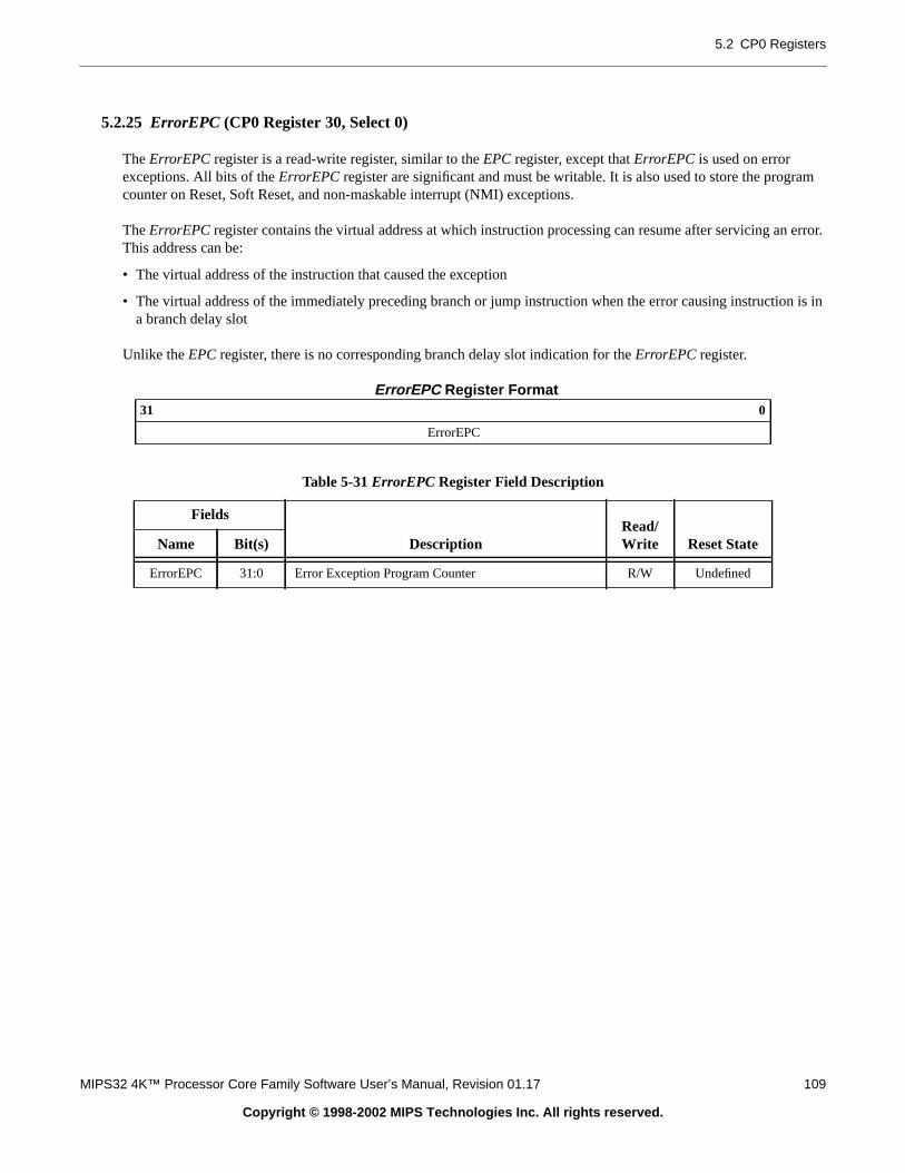
5.2 CP0 Registers
ram
error.
n is in
5.2.25 ErrorEPC (CP0 Register 30, Select 0)
TheErrorEPC register is a read-write register, similar to theEPC register, except thatErrorEPC is used on errorexceptions. All bits of theErrorEPC register are significant and must be writable. It is also used to store the progcounter on Reset, Soft Reset, and non-maskable interrupt (NMI) exceptions.
TheErrorEPC register contains the virtual address at which instruction processing can resume after servicing anThis address can be:
• The virtual address of the instruction that caused the exception
• The virtual address of the immediately preceding branch or jump instruction when the error causing instructioa branch delay slot
Unlike theEPC register, there is no corresponding branch delay slot indication for theErrorEPC register.
ErrorEPC Register Format31 0
ErrorEPC
Table 5-31ErrorEPC Register Field Description
Fields
DescriptionRead/Write Reset StateName Bit(s)
ErrorEPC 31:0 Error Exception Program Counter R/W Undefined
MIPS32 4K™ Processor Core Family Software User’s Manual, Revision 01.17 109
Copyright © 1998-2002 MIPS Technologies Inc. All rights reserved.
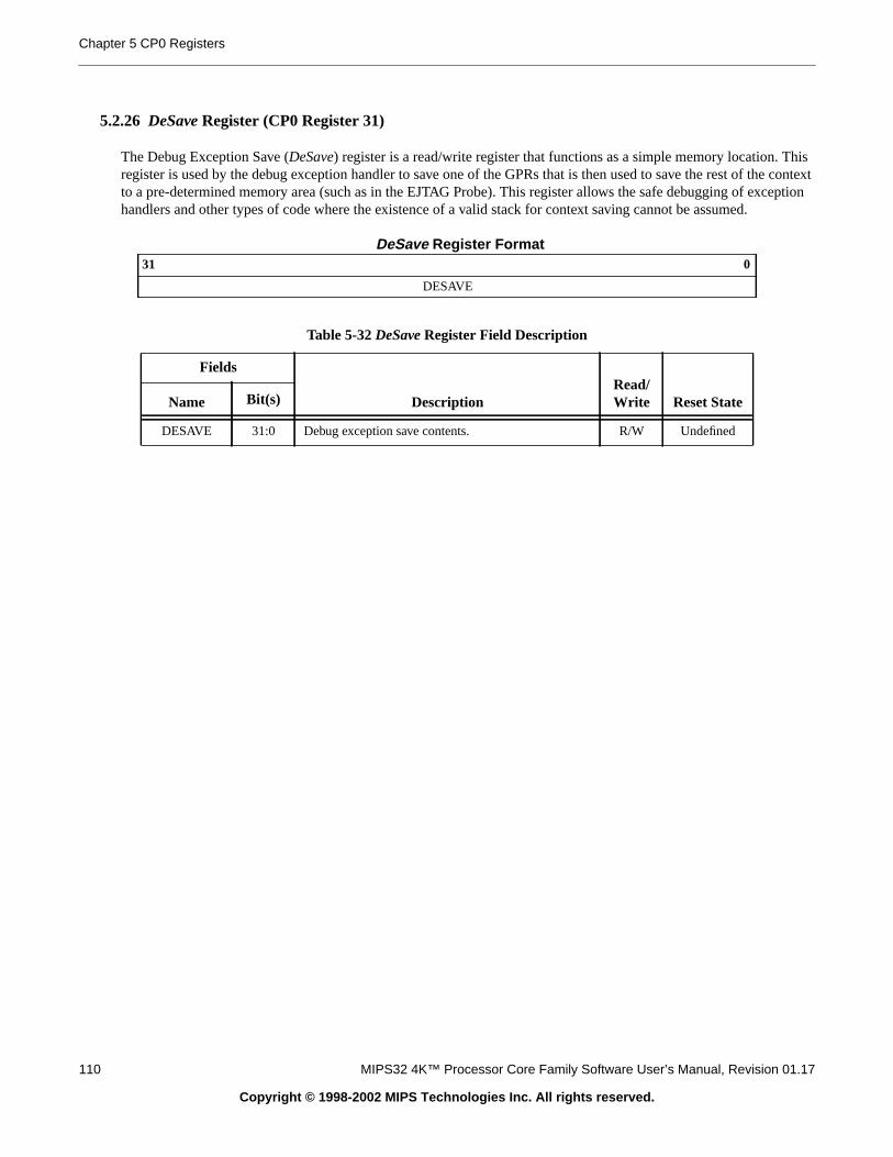
Chapter 5 CP0 Registers
hishe contextception
5.2.26 DeSave Register (CP0 Register 31)
The Debug Exception Save (DeSave) register is a read/write register that functions as a simple memory location. Tregister is used by the debug exception handler to save one of the GPRs that is then used to save the rest of tto a pre-determined memory area (such as in the EJTAG Probe). This register allows the safe debugging of exhandlers and other types of code where the existence of a valid stack for context saving cannot be assumed.
DeSave Register Format31 0
DESAVE
Table 5-32DeSave Register Field Description
Fields
DescriptionRead/Write Reset StateName Bit(s)
DESAVE 31:0 Debug exception save contents. R/W Undefined
110 MIPS32 4K™ Processor Core Family Software User’s Manual, Revision 01.17
Copyright © 1998-2002 MIPS Technologies Inc. All rights reserved.

ftware
of theace. All
y
e
Chapter 6
Hardware and Software Initialization
The MIPS32 4K processor cores have has only a minimal amount of hardware initialization and rely relies on soto fully initialize the device.
This chapter contains the following sections:
• Section 6.1, "Hardware Initialized Processor State"
• Section 6.2, "Software Initialized Processor State"
6.1 Hardware Initialized Processor State
The 4K processor cores, like most MIPS processors, are is not fully initialized by reset. Only a minimal subset processor state is cleared. This is enough to bring the core up while running in unmapped and uncached code spother processor states can then be initialized by software.SI_ColdReset is asserted after power-up to bring the deviceinto a known state. Soft reset can be forced by asserting theSI_Resetpin. This can be used when the device is alreadup and running and does not need as much initialization.
6.1.1 Coprocessor Zero State
Much of the hardware initialization occurs in Coprocessor Zero.
• Random (4Kc core only) - set to maximum value on Reset
• Wired (4Kc core only) - set to 0 on Reset
• StatusBEV - set to 1 on Reset/SoftReset
• StatusTS - cleared to 0 on Reset/SoftReset
• StatusSR - cleared to 0 on Reset, set to 1 on SoftReset
• StatusNMI - cleared to 0 on Reset/SoftReset
• StatusERL - set to 1 on Reset/SoftReset
• StatusRP - cleared to 0 on Reset
• WatchLoI,R,W - cleared to 0 on Reset
• Config fields related to static inputs - set to input value by Reset
• ConfigK0 - set to 010 (uncached) on Reset
• ConfigKU - set to 010 (uncached) on Reset (4Km and 4Kp cores only)
• ConfigK23 - set to 010 (uncached) on Reset (4Km and 4Kp cores only)
• DebugDM- cleared to 0 on Reset/SoftReset (unless EJTAGBOOT option is used to boot into DebugMode, seChapter 9, “EJTAG Debug Support,” for details)
• DebugLSNM - cleared to 0 on Reset/SoftReset
• DebugIBusEP - cleared to 0 on Reset/SoftReset
• DebugDBusEP - cleared to 0 on Reset/SoftReset
MIPS32 4K™ Processor Core Family Software User’s Manual, Revision 01.17 111
Copyright © 1998-2002 MIPS Technologies Inc. All rights reserved.

Chapter 6 Hardware and Software Initialization
y isr-upftware.
et or
Reset.
require
f theut the
. This32/64 twoid this.
he arrayscan
region.
• DebugIEXI - cleared to 0 on Reset/SoftReset
• DebugSSt- cleared to 0 on Reset/SoftReset
6.1.2 TLB Initialization (4Kc core only)
Each 4Kc TLB entry has a “hidden” state bit which is set by Reset/SoftReset and is cleared when the TLB entrwritten. This bit disables matches and prevents “TLB Shutdown” conditions from being generated by the powevalues in the TLB array (when two or more TLB entries match on a single address). This bit is not visible to so
6.1.3 Bus State Machines
All pending bus transactions are aborted and the state machines in the bus interface unit are reset when a ResSoftReset exception is taken.
6.1.4 Static Configuration Inputs
All static configuration inputs (defining the bus mode and cache size for example) should only be changed during
6.1.5 Fetch Address
Upon Reset/SoftReset, unless the EJTAGBOOT option is used, the fetch is directed to VA 0xBFC00000 (PA0x1FC00000). This address is in kseg1,which is unmapped and uncached, so that the TLB and caches do nothardware unitization.
6.2 Software Initialized Processor State
Software is required to initialize the following parts of the device.
6.2.1 Register File
The register file powers up in an unknown state with the exception of r0 which is always 0. Initializing the rest oregister file is not required for proper operation. Good code will generally not read a register before writing to it, bboot code can initialize the register file for added safety.
6.2.2 TLB (4Kc Core Only)
Because of the hidden bit indicating initialization, the 4Kc core does not require TLB initialization upon ColdResetis an implementation specific feature of the 4Kc core and cannot be relied upon if writing generic code for MIPSprocessors. When initializing the TLB, care must be taken to avoid creating a “TLB Shutdown” condition whereTLB entries could match on a single address. Unique virtual addresses should be written to each TLB entry to avo
6.2.3 Caches
The cache tag and data arrays power up to an unknown state and are not affected by reset. Every tag in the cacshould be initialized to an invalid state using the CACHE instruction (typically the Index Invalidate function). Thisbe a long process, especially since the instruction cache initialization needs to be run in an uncached address
112 MIPS32 4K™ Processor Core Family Software User’s Manual, Revision 01.17
Copyright © 1998-2002 MIPS Technologies Inc. All rights reserved.
6.2 Software Initialized Processor State
hat areeptions
y
ritable,be
6.2.4 Coprocessor Zero state
Miscellaneous Cop0 states need to be initialized prior to leaving the boot code. There are various exceptions tblocked by ERL=1 or EXL=1 and that are not cleared by Reset. These can be cleared to avoid taking spurious excwhen leaving the boot code.
• Cause: WP (Watch Pending), SW0/1 (Software Interrupts) should be cleared.
• Config: K0 should be set to the desired Cache Coherency Algorithm (CCA) prior to accessing kseg0.
• Config: (4Km and 4Kp cores only) KU and K23 should be set to the desired CCA for useg/kuseg and kseg2/3respectively prior to accessing those regions.
• Count: Should be set to a known value if Timer Interrupts are used.
• Compare: Should be set to a known value if Timer Interrupts are used. The write to compare will also clear anpending Timer Interrupts (Thus,Count should be set beforeCompare to avoid any unexpected interrupts).
• Status: Desired state of the device should be set.
• Other Cop0 state: Other registers should be written before they are read. Some registers are not explicitly wand are only updated as a by-product of instruction execution or a taken exception. Uninitialized bits should masked off after reading these registers.
MIPS32 4K™ Processor Core Family Software User’s Manual, Revision 01.17 113
Copyright © 1998-2002 MIPS Technologies Inc. All rights reserved.
Chapter 6 Hardware and Software Initialization
114 MIPS32 4K™ Processor Core Family Software User’s Manual, Revision 01.17
Copyright © 1998-2002 MIPS Technologies Inc. All rights reserved.

ime forrences tocur in
size andhe is
ursturned,
severalading
Chapter 7
Caches
This chapter describes the caches present in a MIPS32 4K processor core. It contains the following sections:
• Section 7.1, "Introduction"
• Section 7.2, "Cache Protocols"
• Section 7.3, "Instruction Cache"
• Section 7.4, "Data Cache"
• Section 7.5, "Memory Coherence Issues"
7.1 Introduction
A 4K processor core supports separate instruction and data caches which may be flexibly configured at build tvarious sizes, organizations and set-associativities. The use of separate caches allows instruction and data refeproceed simultaneously. Both caches are virtually indexed and physically tagged, allowing cache access to ocparallel with virtual-to-physical address translation.
The instruction and data caches are independently configured. For example, the data cache can be 2 KBytes in2-way set associative, while the instruction cache can be 8 KBytes in size and 4-way set associative. Each cacaccessed in a single processor cycle.
Cache refills are performed using a 4-word fill buffer, which holds data returned from memory during a 4-beat btransaction. The critical miss word is always returned first. The caches are blocking until the critical word is retbut the pipeline may proceed while the other 3 beats of the burst are still active on the bus.
Table 7-1 lists the instruction and data cache attributes:
Table 7-2shows the cache size and organization options; note that the same total cache size may be achieved withdifferent set-associativities. Software can identify the instruction or data cache configuration on a 4K core by rethe appropriate bits of theConfig1 register; seeSection 5.2.16, "Config1 Register (CP0 Register 16, Select 1)".
Table 7-1 Instruction and Data Cache Attributes
Parameter Instruction Data
Size 0 - 16 KBytes 0 - 16 KBytes
Number of Cache Sets 0, 64, 128 and 256 0, 64, 128 and 256
Lines Per Set (Associativity) 1 - 4 way set associative 1 - 4 way set associative
Line Size 16 Bytes 16 Bytes
Read Unit 32-bits 32-bits
Write Policy N/A write-through withoutwrite-allocate
Miss restart after transfer of miss word miss word
Cache Locking per line per line
MIPS32 4K™ Processor Core Family Software User’s Manual, Revision 01.17 115
Copyright © 1998-2002 MIPS Technologies Inc. All rights reserved.

Chapter 7 Caches
indexed,hysically
ane for totalith therd is
.
7.2 Cache Protocols
7.2.1 Cache Organization
The instruction and data caches each consist of two arrays: a tag array and a data array. The caches are virtuallysince a virtual address is used to select the appropriate line within both the tag and data arrays. The caches are ptagged, as the tag array contains a physical, not virtual, address.
The tag and data arrays holdn ways of information per line, corresponding to then-way set associativity of the cache,wheren can be between 1 and 4 for a cache in a 4K core.Figure 7-1 shows the format of each line of the tag and datarrays for each way. A tag entry consists of the upper 22 bits of the physical address (bits [31:10]), 4 valid bits (oeach data word in the line), a lock bit and a LRF bit. A data entry contains the four 32-bit words in the line, for aof 16 bytes. Not every word need be present in the data array, hence the per-word validity information stored wtag. A word is the minimum valid quanta, so it is not possible to hold a partially valid subword. Once a valid woresident in the cache, byte, halfword or tri-byte stores can update a portion of the word.
Figure 7-1 Cache Array Formats
Table 7-2 Instruction and Data Cache Sizes
Cache Size (bytes) Way Organization Options
0K No cache
1K One 1K way
2KOne 2K way
Two 1K ways
3K Three 1K ways
4K
One 4K way
Two 2K ways
Four 1K ways
6K Three 2K ways
8KTwo 4K ways
Four 2K ways
12K Three 4K ways
16K Four 4K ways
Tag:
Data: Word3 Word2 Word1 Word0
PA Valid L LRF
32 32 32 32
22 4 1 1
116 MIPS32 4K™ Processor Core Family Software User’s Manual, Revision 01.17
Copyright © 1998-2002 MIPS Technologies Inc. All rights reserved.
7.3 Instruction Cache
ddresses
datas is cachemisses
gmentsable
lt in a), the
filledits for entries
zero,0 will
ked,tify the during
ggedaving to
d intoe.
cked or
cacheait for
7.2.2 Cacheability Attributes
All the The 4K cores supports the following cacheability attributes:
• Uncached: Addresses in a memory area indicated as uncached are not read from the cache. Stores to such aare written directly to main memory, without changing cache contents.
• Write-through : Loads and instruction fetches first search the cache, reading main memory only if the desireddoes not reside in the cache. On data store operations, the cache is first searched to see if the target addresresident. If it is resident, the cache contents are updated, and main memory is also written. If the cache lookupon a store, only main memory is written. Hence, the allocation policy on a cache miss is read-allocate only.
Some segments of memory employ a fixed caching policy; for example the kseg1 is always uncacheable. Other seof memory allow the caching policy to be selected by software. Generally, the cache policy for these programmregions is defined by a cacheability attribute field associated with that region of memory. SeeChapter 3, “MemoryManagement,” on page 31 for further details.
7.2.3 Replacement Policy
The replacement policy refers to how a way is chosen to hold an incoming cache line on a miss which will resucache fill, when a cache is at least two-way set associative. In a direct mapped cache (one-way set associativereplacement policy is irrelevant since there is only one way available. The replacement policy is least recently (LRF), first considering invalid ways and excluding any locked ways. On a cache miss, the valid, lock and LRF beach tag entry of the selected line may be used to determine the way which will be chosen. The number of tagwhich are looked at depends on the set associativity of the cache.
First the valid bits are inspected. If an invalid way is available, as determined by all 4 of the valid bits in a tag beingthen that way will be selected. If more than one invalid way is available, then the first one found starting from waybe selected.
If all ways are valid, then any locked ways will be excluded from consideration for replacement. If all ways are locthen no replacement can occur to that line. For the unlocked ways, the LRF bits from each tag are used to idenway which has been filled least recently, and that way is selected for replacement. When the new tag is writtenthe line fill, its LRF bit is modified to indicate that way is no longer the least recently filled.
7.3 Instruction Cache
The instruction cache is an optional on-chip memory block of up to 16 KBytes. The virtually indexed, physically tacache allows the virtual-to-physical address translation to occur in parallel with the cache access rather than hwait for the physical address translation.
All of the cores support instruction cache-locking. Cache locking allows critical code or data segments to be lockethe cache on a “per-line” basis, enabling the system programmer to maximize the efficiency of the system cach
The cache locking function is always enabled on all instruction cache entries. Entries can then be marked as lounlocked on a per entry basis using the CACHE instruction.
7.4 Data Cache
The data cache is an optional on-chip memory block of up to 16 KBytes. The virtually indexed, physically taggedallows the virtual-to-physical address translation to occur in parallel with the cache access rather than having to wthe physical address translation.
MIPS32 4K™ Processor Core Family Software User’s Manual, Revision 01.17 117
Copyright © 1998-2002 MIPS Technologies Inc. All rights reserved.

Chapter 7 Caches
nts to bected for
nlocked
n. Sincehusnce is
ust beent toctuallyocationsuction.
’s write
The core also supports a data cache locking mechanism identical to the instruction cache. Critical data segmelocked into the cache on a “per-line” basis. The locked contents can be updated on a store hit, but cannot be selereplacement on a miss.
The cache locking function is always enabled on all data cache entries. Entries can then be marked as locked or uon a per entry basis using the CACHE instruction.
7.5 Memory Coherence Issues
A cache presents coherency issues within the memory hierarchy which must be considered in the system desiga cache holds a copy of memory data, it is possible for another memory master to modify a memory location, tmaking other copies of that location stale if those copies are still in use. A detailed discussion of memory coherebeyond the scope of this document, but following are a few related comments.
A 4K processor contains no direct hardware support for managing coherency with respect to its caches, so it mhandled via system design or software. The 4K caches are write-through, so all data writes will eventually be smemory. Due to write buffers, however, there could be a delay in how long it takes for the write to memory to aoccur. If another memory master updates cacheable memory which could also be in the 4K caches, then those lmay need to be flushed from the cache. The only way to accomplish this invalidation is by use of the CACHE instr
The SYNC instruction may also be useful to software enforcing memory coherence, as it flushes the 4K processorbuffers.
118 MIPS32 4K™ Processor Core Family Software User’s Manual, Revision 01.17
Copyright © 1998-2002 MIPS Technologies Inc. All rights reserved.

activetruction
. The
r occurs
e
on theg of theruptt or let it
ntthe error
eks.
e as thebug
Chapter 8
Power Management
The MIPS32 4K processor cores offers a number of power management features, including low-power design,power management and power-down modes of operation. The core is a static design that supports a WAIT insdesigned to signal the rest of the device that execution and clocking should be halted, reducing system powerconsumption during idle periods.
The core provides two mechanisms for system level low power support discussed in the following sections.
• Section 8.1, "Register-Controlled Power Management"
• Section 8.2, "Instruction-Controlled Power Management"
8.1 Register-Controlled Power Management
The RP bit in the CP0Statusregister a standard software mechanism for placing the system into a low power statestate of the RP bit is available externally via theSI_RPsignal. Three additional pins,SI_EXL, SI_ERL, andEJ_DebugMsupport the power management function by allowing the user to change the power state if an exception or errowhile the core is in a low power state.
Setting the RP bit of the CP0Statusregister causes the core to assert theSI_RPsignal. The external agent can then decidwhether to reduce the clock frequency and place the core into power down mode.
If an interrupt is taken while the device is in power down mode, that interrupt may need to be serviced dependingneeds of the application. The interrupt causes an exception which in turn causes the EXL bit to be set. The settinEXL bit causes the assertion of theSI_EXL signal on the external bus, indicating to the external agent that an interhas occurred. At this time the external agent can choose to either speed up the clocks and service the interrupbe serviced at the lower clock speed.
The setting of the ERL bit causes the assertion of theSI_ERLsignal on the external bus, indicating to the external agethat an error has occurred. At this time the external agent can choose to either speed up the clocks and serviceor let it be serviced at the lower clock speed.
Similarly, theEJ_DebugM signal indicates that the processor is in debug mode. Debug mode is entered when thprocessor takes a debug exception. If fast handling of this is desired, the external agent can speed up the cloc
The core provides four power down signals that are part of the system interface. Three of the pins change statcorresponding bits in the CP0Status register are set or cleared. The fourth pin indicates that the processor is in demode.
• TheSI_RP signal represents the state of the RP bit (27) in the CP0Status register.
• TheSI_EXL signal represents the state of the EXL bit (1) in the CP0Status register.
• TheSI_ERL signal represents the state of the ERL bit (2) in the CP0Status register.
• TheEJ_DebugM signal indicates that the processor has entered debug mode.
MIPS32 4K™ Processor Core Family Software User’s Manual, Revision 01.17 119
Copyright © 1998-2002 MIPS Technologies Inc. All rights reserved.

Chapter 8 Power Management
idleipeline
stallser
ode and
8.2 Instruction-Controlled Power Management
The second mechanism for invoking power down mode is through execution of the WAIT instruction. If the bus isat the time the WAIT instruction reaches the M stage of the pipeline, the internal clocks are suspended and the pis frozen. However, the internal timer and some of the input pins (SI_Int[5:0], SI_NMI, SI_Reset, SI_ColdReset, andEJ_DINT) continue to run. If the bus is not idle at the time the WAIT instruction reaches the M stage, the pipelineuntil the bus becomes idle, at which time the clocks are stopped. Once the CPU is in instruction controlled powmanagement mode, any enabled interrupt, NMI, debug interrupt, or reset condition causes the CPU to exit this mresume normal operation. While the part is in this low-power mode, theSI_SLEEP signal is asserted to indicate toexternal agents what the state of the chip is.
120 MIPS32 4K™ Processor Core Family Software User’s Manual, Revision 01.17
Copyright © 1998-2002 MIPS Technologies Inc. All rights reserved.

Chapter 9
EJTAG Debug Support
The EJTAG debug logic in the MIPS32 4K processor cores provides two optional modules: one for hardwarebreakpoints, and the other is a Test Access Port (TAP) for a dedicated connection to a debug host.
This chapter contains the following sections.
• Section 9.1, "Debug Control Register"
• Section 9.2, "Hardware Breakpoints"
• Section 9.3, "Test Access Port (TAP)"
• Section 9.4, "EJTAG TAP Registers"
• Section 9.5, "Processor Accesses"
MIPS32 4K™ Processor Core Family Software User’s Manual, Revision 01.17 121
Copyright © 1998-2002 MIPS Technologies Inc. All rights reserved.

Chapter 9 EJTAG Debug Support
ftware
to the and a
asking on noy causeonsult
gw takes
9.1 Debug Control Register
The Debug Control Register (DCR) register controls and provides information about debug issues, and is alwaysprovided with the CPU core. The register is memory mapped in drseg at offset 0x0.
The DataBrk and InstBrk bits indicates if hardware breakpoints are included in the implementation, and debug sois expected to read hardware breakpoint registers for additional information.
Hardware and software interrupts are maskable for non-debug mode with the INTE bit, which works in additionother mechanisms for interrupt masking and enabling. NMI is maskable in non-debug mode with the NMIE bit,pending NMI is indicated through the NMIP bit.
The SRE bit allows implementation dependent masking of none, some or all sources for soft reset. The soft reset mmay only be applied to a soft reset source, if that source can be efficiently masked in the system, thus resultingreset at all. If that is not possible, then that soft reset source should not be masked, since a “half” soft reset mathe system to fail or hang. There is no automatic indication of whether the SRE is effective, but the user must csystem documentation.
The PE bit reflects the ProbEn bit from the EJTAG Control register (ECR), whereby the probe can indicate to the debusoftware running on the CPU if the probe expects to service dmseg accesses. The reset value in the table beloeffect on both hard and soft reset.
Debug Control Register31 30 29 28 18 17 16 15 5 4 3 2 1 0
Res ENM Res DB IB Res INTE NMIE NMIP SRE PE
Table 9-1Debug Control Register Field Descriptions
Fields
DescriptionRead/Write Reset StateName Bit(s)
Res 31:30 reserved R 0
ENM 29
Endianess in Kernel and Debug mode. This bit indicatesthe endianess in Kernel and Debug mode.
0: Little Endian1: Big Endian
R Preset
Res 28:18 reserved R 0
DB 17
Data Break Implemented. This bit indicates if the DataBreak feature is implemented.
0: No Data Break feature implemented1: Data Break feature is implemented
R Preset
IB 16
Instruction Break Implemented. This bit indicates if theInstruction Break feature is implemented.
0: No Instruction Break feature implemented1: Instruction Break feature is implemented
R Preset
Res 15:5 reserved R 0
122 MIPS32 4K™ Processor Core Family Software User’s Manual, Revision 01.17
Copyright © 1998-2002 MIPS Technologies Inc. All rights reserved.
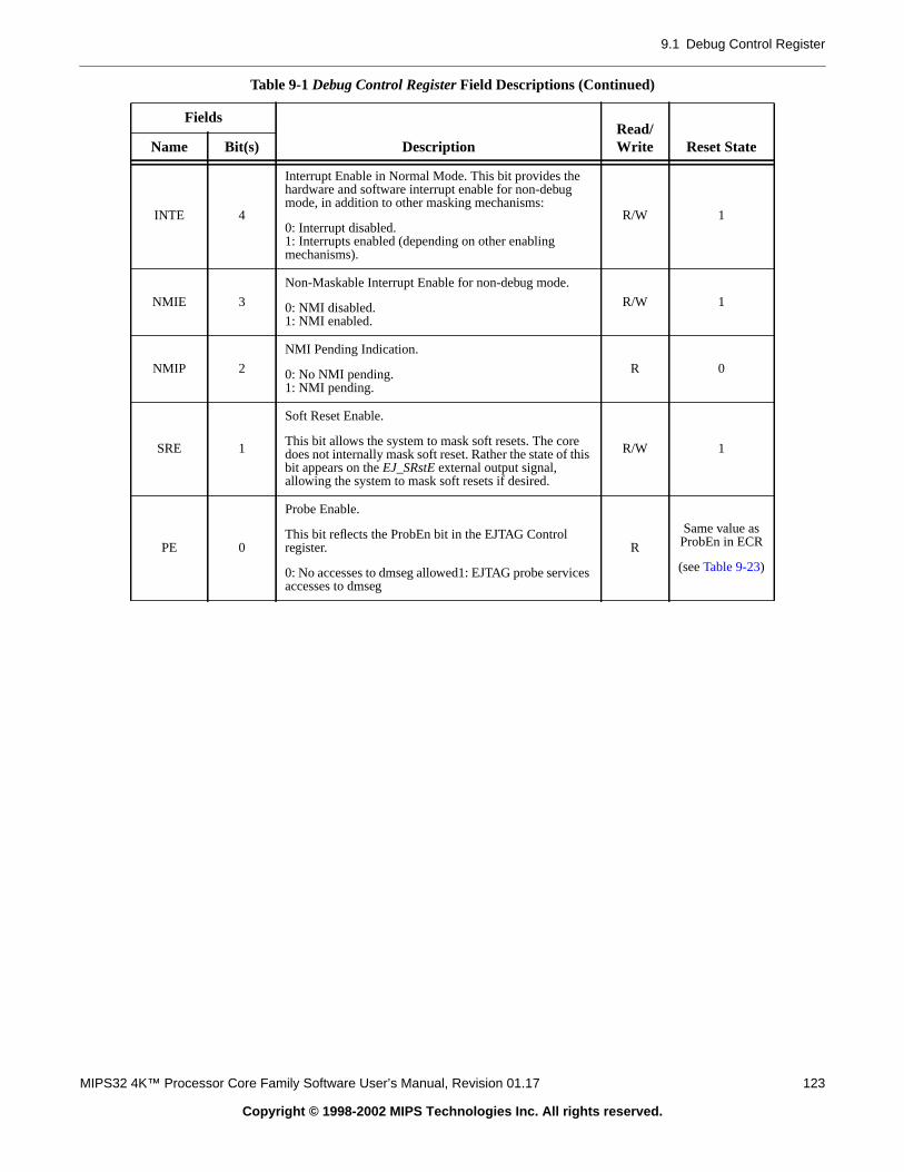
9.1 Debug Control Register
INTE 4
Interrupt Enable in Normal Mode. This bit provides thehardware and software interrupt enable for non-debugmode, in addition to other masking mechanisms:
0: Interrupt disabled.1: Interrupts enabled (depending on other enablingmechanisms).
R/W 1
NMIE 3
Non-Maskable Interrupt Enable for non-debug mode.
0: NMI disabled.1: NMI enabled.
R/W 1
NMIP 2
NMI Pending Indication.
0: No NMI pending.1: NMI pending.
R 0
SRE 1
Soft Reset Enable.
This bit allows the system to mask soft resets. The coredoes not internally mask soft reset. Rather the state of thisbit appears on theEJ_SRstE external output signal,allowing the system to mask soft resets if desired.
R/W 1
PE 0
Probe Enable.
This bit reflects the ProbEn bit in the EJTAG Controlregister.
0: No accesses to dmseg allowed1: EJTAG probe servicesaccesses to dmseg
R
Same value asProbEn in ECR
(seeTable 9-23)
Table 9-1Debug Control Register Field Descriptions (Continued)
Fields
DescriptionRead/Write Reset StateName Bit(s)
MIPS32 4K™ Processor Core Family Software User’s Manual, Revision 01.17 123
Copyright © 1998-2002 MIPS Technologies Inc. All rights reserved.
Chapter 9 EJTAG Debug Support
actions. a debugand areguish
Data
een the core
gisters
ruction
ar to thebased onre value.
9.2 Hardware Breakpoints
Hardware breakpoints provide for the comparison by hardware of executed instructions and data load/store transIt is possible to set instruction breakpoints on addresses even in ROM area, and set data breakpoints to causeexception on a specific data transaction. Instruction and data hardware breakpoints are alike for may aspects, thus described in parallel in the following. The term hardware is not applied to breakpoint, unless required to distinit from software breakpoint.
There are two types of simple hardware breakpoints implemented in the 4K cores: Instruction breakpoints andbreakpoints.
Each core can be configured with the following breakpoint options:
• No data or instruction breakpoints
• Two instruction and one data breakpoint
• Four instruction and two data breakpoints
9.2.1 Features of Instruction Breakpoint
Instruction breaks occur on instruction fetch operations and the break is set on the virtual address on the bus betwCPU and the instruction cache. Instruction breaks can also be made on the ASID value used by the MMU (4Kconly). Finally, a mask can be applied to the virtual address to set breakpoints on a range of instructions.
Instruction breakpoints compare the virtual address of the executed instructions (PC) and the ASID, with the refor each instruction breakpoint including masking of address and ASID. An overview is shown inFigure 9-1andFigure9-2.
Figure 9-1 Instruction Hardware Breakpoint Overview (4Kc Core)
Figure 9-2 Instruction Hardware Breakpoint Overview (4Km and 4Kp Core)
When a instruction breakpoint matches, a debug exception and/or a trigger is generated. An internal bit in the instbreakpoint registers is set to indicate that the match occurred.
9.2.2 Features of Data Breakpoint
Data breakpoints occur on load/store transactions. Breakpoints are set on virtual address and ASID values, similInstruction breakpoint. Data breakpoints can be set on a load, a store or both. Data breakpoints can also be setthe value of the load/store operation. Finally, masks can be applied to both the virtual address and the load/sto
Trigger Indication
PC
ASID
InstructionHardwareBreakpoint
Debug Exception
Trigger IndicationPC
InstructionHardwareBreakpoint
Debug Exception
124 MIPS32 4K™ Processor Core Family Software User’s Manual, Revision 01.17
Copyright © 1998-2002 MIPS Technologies Inc. All rights reserved.
9.2 Hardware Breakpoints
sactionpoint
taception
ception
n. The
Data breakpoints compare the transaction type (TYPE), which may be load or store, the virtual address of the tran(ADDR), the ASID, accessed bytes (BYTELANE) and data value (DATA), with the registers for each data breakincluding masking or qualification on the transaction properties. An overview is shown inFigure 9-3 andFigure 9-4.
Figure 9-3 Data Hardware Breakpoint Overview (4Kc Core)
Figure 9-4 Data Hardware Breakpoint Overview (4Km/4Kp Core)
When a data breakpoint matches, a debug exception and/or a trigger is generated, and an internal bit in the dabreakpoint registers is set to indicate that the match occurred. The match is either precise whereby the debug exor trigger occurs on the instruction that caused the breakpoint to match, or it is imprecise whereby the debug exor trigger occurs later in the program flow.
9.2.3 Overview of Registers for Instruction Breakpoints
The register with implementation indication and status for instruction breakpoints in general is shown inTable 9-2.
The four instruction breakpoints are numbered 0 to 3 for registers and breakpoints, and the number is indicated byregisters for each breakpoint are shown inTable 9-3.
Table 9-2 Overview of Status Register for Instruction Breakpoints
Register Mnemonic Register Name and Description
IBS Instruction Breakpoint Status
Table 9-3 Overview of Registers for each Instruction Breakpoint
Register Mnemonic Register Name and Description
IBAn Instruction Breakpoint Address n
IBMn Instruction Breakpoint Address Mask n
IBASIDn Instruction Breakpoint ASID n (4Kc core)
IBCn Instruction Breakpoint Control n
Data HardwareBreakpoint
Debug Exception
Trigger IndicationASID
ADDR
TYPE
BYTELANE
DATA
Data HardwareBreakpoint
Debug Exception
Trigger Indication
ADDR
TYPE
BYTELANE
DATA
MIPS32 4K™ Processor Core Family Software User’s Manual, Revision 01.17 125
Copyright © 1998-2002 MIPS Technologies Inc. All rights reserved.

Chapter 9 EJTAG Debug Support
n. The
nts only
TE bits
ction inh. Thealigned
it level,e thetation.
match
9.2.4 Registers for Data Breakpoint Setup
The register with implementation indication and status for data breakpoints in general is shown inTable 9-4.
The two data breakpoints are numbered 0 and 1 for registers and breakpoints, and the number is indicated byregisters for each breakpoint are shown inTable 9-5.
9.2.5 Conditions for Matching Breakpoints
A number of conditions must be fulfilled in order for a breakpoint to match on an executed instruction or a datatransaction, and the conditions for matching instruction and data breakpoints are described below. The breakpoimatch for instructions executed in non-debug mode, thus never on instructions executed in debug mode.
The match of an enabled breakpoint can either generate a debug exception or a trigger indication. The BE and/orin theIBCn or DBCn registers are used to enable the breakpoints.
Debug software should not configure breakpoints to compare on ASID value, unless a TLB is present in theimplementation (4Kc core only).
9.2.5.1 Conditions for Matching Instruction Breakpoint
When an instruction breakpoint is enabled, that breakpoint is evaluated for the address of every executed instrunon-debug mode, including execution of instructions at an address causing an address error on instruction fetcbreakpoint is not evaluated on instructions from speculative fetch or execution, nor for addresses which are unwith an executed instruction.
Match of the breakpoint depends on the virtual address of the executed instruction (PC) which can be masked at band match may also include optional compare of ASID value. The registers for each instruction breakpoint havvalues and mask used in the compare, and the equation that determines the match is shown below in C-like no
IB_match =( ! IBCn ASIDuse || ( ASID == IBASIDn ASID ) ) &&( <all 1’s> == ( IBMnIBM | ~ ( PC ^ IBAn IBA ) )
The match indication for instruction breakpoints is always precise, i.e. indicated on the instruction causing the IB_to be true.
Table 9-4 Overview of Status Register for Data Breakpoints
Register Mnemonic Register Name and Description
DBS Data Breakpoint Status
Table 9-5 Overview of Registers for each Data Breakpoint
Register Mnemonic Register Name and Description
DBAn Data Breakpoint Address n
DBMn Data Breakpoint Address Mask n
DBASIDn Data Breakpoint ASID n (4Kc core)
DBCn Data Breakpoint Control n
DBVn Data Breakpoint Value n
126 MIPS32 4K™ Processor Core Family Software User’s Manual, Revision 01.17
Copyright © 1998-2002 MIPS Technologies Inc. All rights reserved.
9.2 Hardware Breakpoints
truction on dataplicittination
the datand the
ue, and, and
NE asmpare is
ATA) istchup of the
ad/storematch
e, as
9.2.5.2 Conditions for Matching Data Breakpoints
When a data breakpoint is enabled, that breakpoint is evaluated for every data transaction due to a load/store insexecuted in non-debug mode, including load/store for coprocessor, and transactions causing an address erroraccess. The breakpoint is not evaluated due to PREF instruction or other transactions which are not part of exload/store transactions in the execution flow, nor for addresses which are not the explicit load/store source or desaddress.
Match of the breakpoint depends on the transaction type (TYPE) as load or store, the address, and optionally value of a transaction. The registers for each data breakpoint has the values and mask used in the compare, aequations that determine the match are shown below in C-like notation.
The overall match equation is DB_match:
DB_match =( ( ( TYPE == load ) && ! DBCnNoLB ) ||
( ( TYPE == store ) && ! DBCnNoSB ) ) &&DB_addr_match && ( DB_no_value_compare || DB_value_match )
Match on the address part, DB_addr_match, depends on virtual address of the transaction (ADDR), the ASID valthe accessed bytes (BYTELANE) where BYTELANE[0] is 1 only if the byte at bits [7:0] on the bus is accessedBYTELANE[1] is 1 only if byte at bits [15:8] is accessed, etc. The DB_addr_match is shown below.
DB_addr_match =( ! DBCnASIDuse || ( ASID == DBASIDnASID ) ) &&( <all 1’s> == ( DBMnDBM | ~ ( ADDR ^ DBAnDBA ) ) ) &&( <all 0’s> != ( ~ BAI & BYTELANE ) )
The size ofDBCnBAI and BYTELANE is 4 bits.
Data value compare is included in the match condition for the data breakpoint depending on the bytes (BYTELAdescribed above) accessed by the transaction, and the contents of breakpoint registers. The DB_no_value_coshown below.
DB_no_value_compare =( <all 1’s> == ( DBCnBLM | DBCnBAI | ~ BYTELANE ) )
The size ofDBCnBLM, DBCnBAI, and BYTELANE is 4 bits.
In case data value compare is required, DB_no_value_compare is false, then the data value from the data bus (Dcompared and masked with the registers for the data breakpoint. The endianess is not considered in these maequations for value, as the compare uses the data bus value directly, thus debug software is responsible for setbreakpoint corresponding with endianess.
DB_value_match =( ( DATA[7:0] == DBVnDBV[7:0] ) || ! BYTELANE[0] || DBCnBLM[0] || DBCnBAI[0] ) &&( ( DATA[15:8] == DBVnDBV[15:8] ) || ! BYTELANE[1] || DBCnBLM[1] || DBCnBAI[1] ) &&( ( DATA[23:16] == DBVnDBV[23:16] ) || ! BYTELANE[2] || DBCnBLM[2] || DBCnBAI[2] )&&( ( DATA[31:24] == DBVnDBV[31:24] ) || ! BYTELANE[3] || DBCnBLM[3] || DBCnBAI[3] )
The match for a data breakpoint is always precise, since the match expression is fully evaluated at the time the loinstruction is executed. A true DB_match can thereby be indicated on the very same instruction causing the DB_to be true.
9.2.6 Debug Exceptions from Breakpoints
Instruction and data breakpoints may be set up to generate a debug exception when the match condition is trudescribed below.
MIPS32 4K™ Processor Core Family Software User’s Manual, Revision 01.17 127
Copyright © 1998-2002 MIPS Technologies Inc. All rights reserved.
Chapter 9 EJTAG Debug Support
tch
load oriving a
ection,
tion.
nd the
s not
value is
ecuted,result
a debug
bug
ug
ction iscurredable to
9.2.6.1 Debug Exception by Instruction Breakpoint
If the breakpoint is enabled by BE in theIBCn register, then a debug instruction break exception occurs if the IB_maequation is true. The corresponding BS[n] bit in theIBS register is set when the breakpoint generates the debugexception.
The debug instruction break exception is always precise, so theDEPCregister and DBD bit in theDebugregister pointsto the instruction that caused the IB_match equation to be true.
The instruction receiving the debug exception does not update any registers due to the instruction, nor does anystore by that instruction occur. Thus a debug exception from a data breakpoint can not occur for instructions recedebug instruction break exception.
The debug handler usually returns to the instruction causing the debug instruction break exception, whereby thinstruction is executed. Debug software is responsible for disabling the breakpoint when returning to the instruotherwise the debug instruction break exception reoccurs.
9.2.6.2 Debug Exception by Data Breakpoint
If the breakpoint is enabled by BE in theDBCn register, then a debug exception occurs when the DB_match condiis true. The corresponding BS[n] bit in theDBS register is set when the breakpoint generates the debug exception
A debug data break exception occurs when a data breakpoint indicates a match. In this case theDEPCregister and DBDbit in theDebug register points to the instruction that caused the DB_match equation to be true.
The instruction causing the debug data break exception does not update any registers due to the instruction, afollowing applies to the load or store transaction causing the debug exception:
• A store transaction is not allowed to complete the store to the memory system.
• A load transaction with no data value compare, i.e. where the DB_no_value_compare is true for the match, iallowed to complete the load.
• A load transaction for a breakpoint with data value compare must occur from the memory system, since the required in order to evaluate the breakpoint.
The result of this is that the load or store instruction causing the debug data break exception appears as not exwith the exception that a load from the memory system do occur for a breakpoint with data value compare, but theof this load is discarded since the register file is not updated by the load.
If both data breakpoints without and with data value compare would match the same transaction and generateexception, then the following rules apply with respect to updating the BS[n] bits.
• On both a load and store the BS[n] bits are required to be set for all matching breakpoints without data valuecompare.
• On a store then BS[n] bits are allowed but not required to be set for all matching breakpoints with data valuecompare, but either all or none of the BS[n] bits must be set for these breakpoints.
• On a load then no of the BS[n] bits are allowed to be set, since the load is not allowed to occur due to the deexception from a breakpoint without data value compare, and a valid data value is therefore not returned.
Any BS[n] bit set prior to the match and debug exception are kept set, since BS[n] bits are only cleared by debsoftware.
The debug handler usually returns to the instruction causing the debug data break exception, whereby the instrure-executed. This re-execution may result in a repeated load from system memory, since the load may have ocpreviously in order to evaluate the breakpoint as described above. I/O devices with side effects on load must be
128 MIPS32 4K™ Processor Core Family Software User’s Manual, Revision 01.17
Copyright © 1998-2002 MIPS Technologies Inc. All rights reserved.
9.2 Hardware Breakpoints
on suche the
generate
s, only
allow such reloads, or debug software should alternatively avoid setting data breakpoint with data value compareI/O devices. Debug software is responsible for disabling breakpoints when returning to the instruction, otherwisdebug data break exception will reoccur.
9.2.7 Breakpoint used as Triggerpoint
Both instruction and data hardware breakpoints may be set up by software so a matching breakpoint does nota debug exception, but only an indications through the BS[n] bit. The TE bit in theIBCnor DBCnregister controls if ainstruction respectively data breakpoint is used as a so-called triggerpoint. The triggerpoints are, like breakpointcompared for instructions executed in non-debug mode.
The BS[n] bit in theIBS or DBS register is set when the respective IB_match or DB_match bit is true.
MIPS32 4K™ Processor Core Family Software User’s Manual, Revision 01.17 129
Copyright © 1998-2002 MIPS Technologies Inc. All rights reserved.
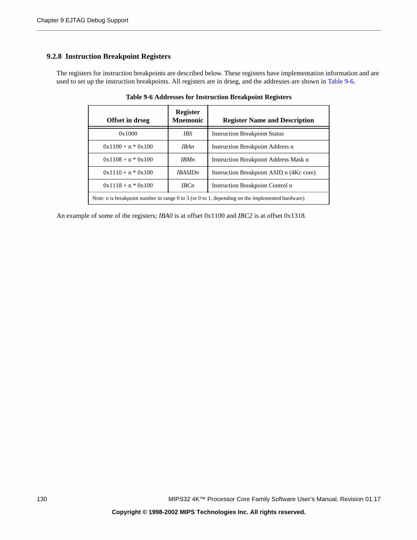
Chapter 9 EJTAG Debug Support
and are
9.2.8 Instruction Breakpoint Registers
The registers for instruction breakpoints are described below. These registers have implementation informationused to set up the instruction breakpoints. All registers are in drseg, and the addresses are shown inTable 9-6.
An example of some of the registers;IBA0 is at offset 0x1100 andIBC2 is at offset 0x1318.
Table 9-6 Addresses for Instruction Breakpoint Registers
Offset in drsegRegister
Mnemonic Register Name and Description
0x1000 IBS Instruction Breakpoint Status
0x1100 + n * 0x100 IBAn Instruction Breakpoint Address n
0x1108 + n * 0x100 IBMn Instruction Breakpoint Address Mask n
0x1110 + n * 0x100 IBASIDn Instruction Breakpoint ASID n (4Kc core)
0x1118 + n * 0x100 IBCn Instruction Breakpoint Control n
Note: n is breakpoint number in range 0 to 3 (or 0 to 1, depending on the implemented hardware)
130 MIPS32 4K™ Processor Core Family Software User’s Manual, Revision 01.17
Copyright © 1998-2002 MIPS Technologies Inc. All rights reserved.
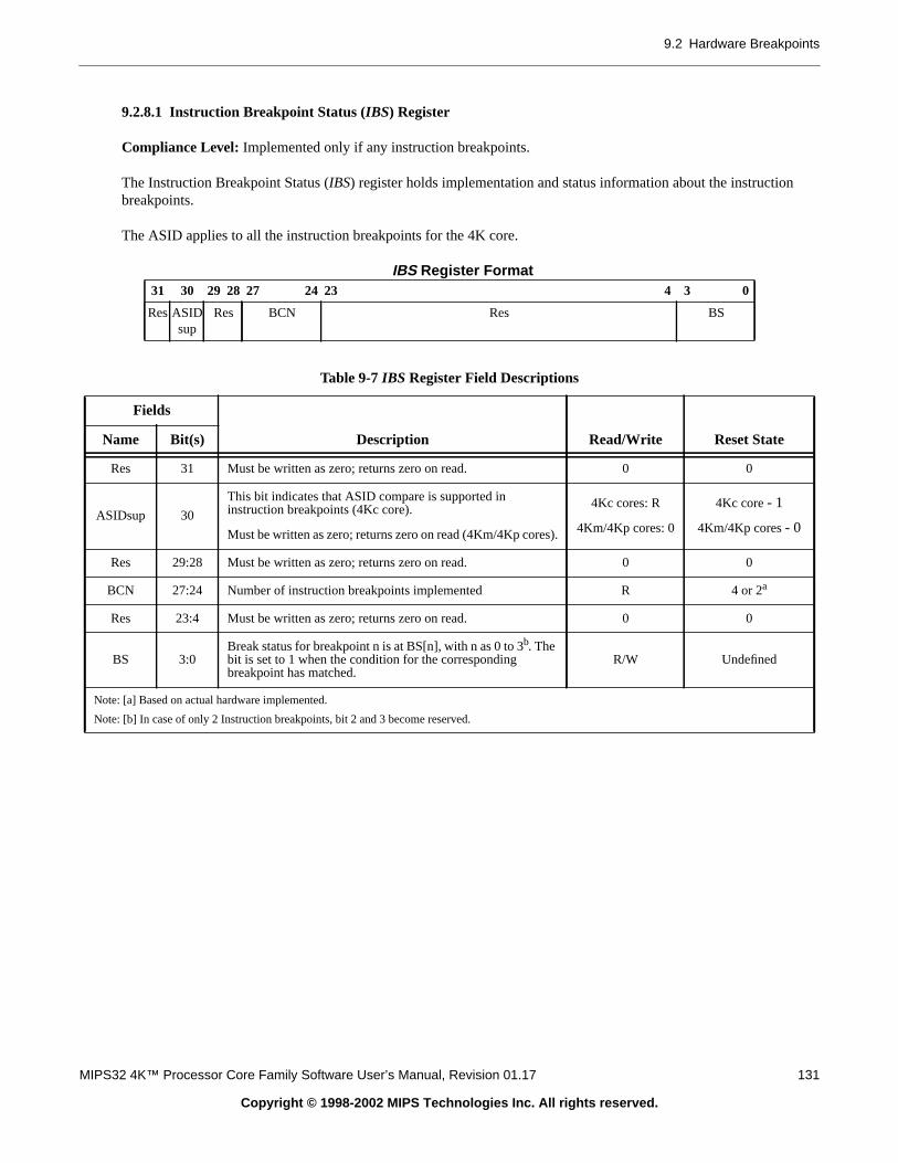
9.2 Hardware Breakpoints
9.2.8.1 Instruction Breakpoint Status (IBS) Register
Compliance Level: Implemented only if any instruction breakpoints.
The Instruction Breakpoint Status (IBS) register holds implementation and status information about the instructionbreakpoints.
The ASID applies to all the instruction breakpoints for the 4K core.
IBS Register Format31 30 29 28 27 24 23 4 3 0
Res ASIDsup
Res BCN Res BS
Table 9-7IBS Register Field Descriptions
Fields
Description Read/Write Reset StateName Bit(s)
Res 31 Must be written as zero; returns zero on read. 0 0
ASIDsup 30
This bit indicates that ASID compare is supported ininstruction breakpoints (4Kc core).
Must be written as zero; returns zero on read (4Km/4Kp cores).
4Kc cores: R
4Km/4Kp cores: 0
4Kc core- 1
4Km/4Kp cores- 0
Res 29:28 Must be written as zero; returns zero on read. 0 0
BCN 27:24 Number of instruction breakpoints implemented R 4 or 2a
Res 23:4 Must be written as zero; returns zero on read. 0 0
BS 3:0Break status for breakpoint n is at BS[n], with n as 0 to 3b. Thebit is set to 1 when the condition for the correspondingbreakpoint has matched.
R/W Undefined
Note: [a] Based on actual hardware implemented.
Note: [b] In case of only 2 Instruction breakpoints, bit 2 and 3 become reserved.
MIPS32 4K™ Processor Core Family Software User’s Manual, Revision 01.17 131
Copyright © 1998-2002 MIPS Technologies Inc. All rights reserved.

Chapter 9 EJTAG Debug Support
nt n.
9.2.8.2 Instruction Breakpoint Address n (IBAn ) Register
Compliance Level: Implemented only for implemented instruction breakpoints.
The Instruction Breakpoint Address n (IBAn) register has the address used in the condition for instruction breakpoi
IBAn Register Format31 0
IBA
Table 9-8IBAn Register Field Descriptions
Fields
DescriptionRead/Write Reset StateName Bit(s)
IBA 31:0 Instruction breakpoint address for condition R/W Undefined
132 MIPS32 4K™ Processor Core Family Software User’s Manual, Revision 01.17
Copyright © 1998-2002 MIPS Technologies Inc. All rights reserved.

9.2 Hardware Breakpoints
for
9.2.8.3 Instruction Breakpoint Address Mask n (IBMn ) Register
Compliance Level: Implemented only for implemented instruction breakpoints.
The Instruction Breakpoint Address Mask n (IBMn) register has the mask for address compare used in the conditioninstruction breakpoint n.
IBMn Register Format31 0
IBM
Table 9-9IBMn Register Field Descriptions
Fields
DescriptionRead/Write Reset StateName Bit(s)
IBM 31:0
Instruction breakpoint address mask for condition:
0: Corresponding address bit not masked
1: Corresponding address bit masked
R/W Undefined
MIPS32 4K™ Processor Core Family Software User’s Manual, Revision 01.17 133
Copyright © 1998-2002 MIPS Technologies Inc. All rights reserved.
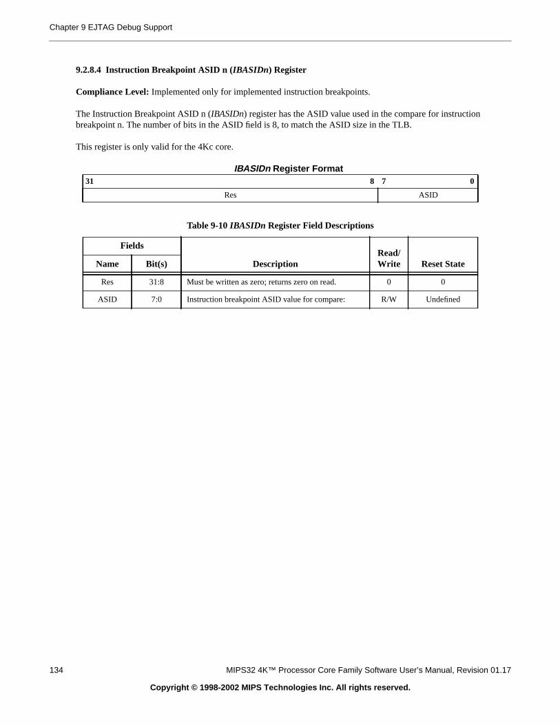
Chapter 9 EJTAG Debug Support
9.2.8.4 Instruction Breakpoint ASID n (IBASIDn ) Register
Compliance Level:Implemented only for implemented instruction breakpoints.
The Instruction Breakpoint ASID n (IBASIDn) register has the ASID value used in the compare for instructionbreakpoint n. The number of bits in the ASID field is 8, to match the ASID size in the TLB.
This register is only valid for the 4Kc core.
IBASIDn Register Format31 8 7 0
Res ASID
Table 9-10IBASIDn Register Field Descriptions
Fields
DescriptionRead/Write Reset StateName Bit(s)
Res 31:8 Must be written as zero; returns zero on read. 0 0
ASID 7:0 Instruction breakpoint ASID value for compare: R/W Undefined
134 MIPS32 4K™ Processor Core Family Software User’s Manual, Revision 01.17
Copyright © 1998-2002 MIPS Technologies Inc. All rights reserved.

9.2 Hardware Breakpoints
9.2.8.5 Instruction Breakpoint Control n (IBCn) Register
Compliance Level: Implemented only for implemented instruction breakpoints.
The Instruction Breakpoint Control n (IBCn) register controls setup of instruction breakpoint n.
IBCn Register Format31 24 23 22 3 2 1 0
Res ASIDuse
Res TE Res BE
Table 9-11IBCn Register Field Descriptions
Fields
DescriptionRead/Write Reset StateName Bits
Res 31:24 Must be written as zero; returns zero on read. 0 0
ASIDuse 23
Use ASID value in compare for instruction breakpoint n (4Kccore):
0: Don’t use ASID value in compare
1: Use ASID value in compare
Must be written as zero; returns zero on read (4Km/4Kp cores).
4Kc core- R/W
4Km/4Kp cores - 0Undefined
Res 22:3 Must be written as zero; returns zero on read. 0 0
TE 2
Use instruction breakpoint n as triggerpoint:
0: Don’t use it as triggerpoint
1: Use it as triggerpoint
R/W 0
Res 1 Must be written as zero; returns zero on read. 0 0
BE 0
Use instruction breakpoint n as breakpoint:
0: Don’t use it as breakpoint
1: Use it as breakpoint
R/W 0
MIPS32 4K™ Processor Core Family Software User’s Manual, Revision 01.17 135
Copyright © 1998-2002 MIPS Technologies Inc. All rights reserved.

Chapter 9 EJTAG Debug Support
used to
9.2.9 Data Breakpoint Registers
The registers for data breakpoints are described below. These registers have implementation information and areset up the data breakpoints. All registers are in drseg, and the addresses are shown in sectionTable 9-12.
An example of some of the registers;DBM0 is at offset 0x2108 andDBV1 is at offset 0x2220.
Table 9-12 Addresses for Data Breakpoint Registers
Offset in drsegRegister
Mnemonic Register Name and Description
0x2000 DBS Data Breakpoint Status
0x2100 + 0x100 * n DBAn Data Breakpoint Address n
0x2108 + 0x100 * n DBMn Data Breakpoint Address Mask n
0x2110 + 0x100 * n DBASIDn Data Breakpoint ASID n (4K core)
0x2118 + 0x100 * n DBCn Data Breakpoint Control n
0x2120 + 0x100 * n DBVn Data Breakpoint Value n
Note: n is breakpoint number as 0 or 1 (or just 0, depending on the implemented hardware)
136 MIPS32 4K™ Processor Core Family Software User’s Manual, Revision 01.17
Copyright © 1998-2002 MIPS Technologies Inc. All rights reserved.
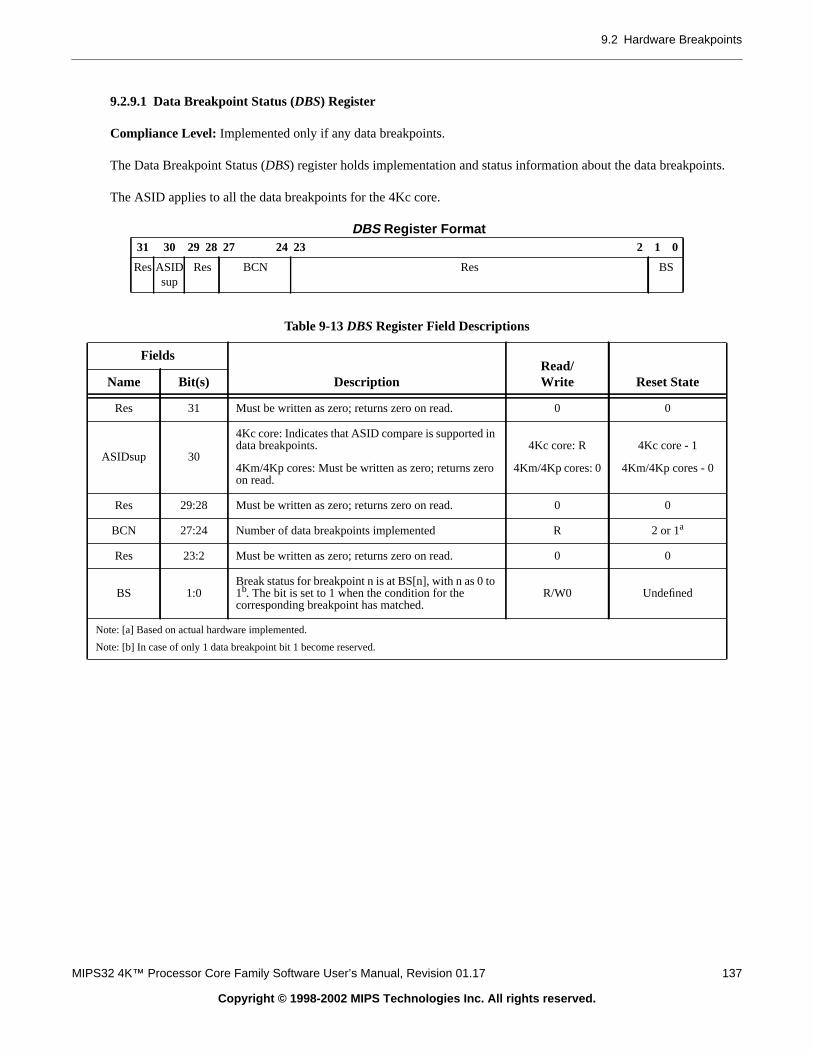
9.2 Hardware Breakpoints
ts.
9.2.9.1 Data Breakpoint Status (DBS) Register
Compliance Level: Implemented only if any data breakpoints.
The Data Breakpoint Status (DBS) register holds implementation and status information about the data breakpoin
The ASID applies to all the data breakpoints for the 4Kc core.
DBS Register Format31 30 29 28 27 24 23 2 1 0
Res ASIDsup
Res BCN Res BS
Table 9-13DBS Register Field Descriptions
Fields
DescriptionRead/Write Reset StateName Bit(s)
Res 31 Must be written as zero; returns zero on read. 0 0
ASIDsup 30
4Kc core: Indicates that ASID compare is supported indata breakpoints.
4Km/4Kp cores: Must be written as zero; returns zeroon read.
4Kc core: R
4Km/4Kp cores: 0
4Kc core - 1
4Km/4Kp cores - 0
Res 29:28 Must be written as zero; returns zero on read. 0 0
BCN 27:24 Number of data breakpoints implemented R 2 or 1a
Res 23:2 Must be written as zero; returns zero on read. 0 0
BS 1:0Break status for breakpoint n is at BS[n], with n as 0 to1b. The bit is set to 1 when the condition for thecorresponding breakpoint has matched.
R/W0 Undefined
Note: [a] Based on actual hardware implemented.
Note: [b] In case of only 1 data breakpoint bit 1 become reserved.
MIPS32 4K™ Processor Core Family Software User’s Manual, Revision 01.17 137
Copyright © 1998-2002 MIPS Technologies Inc. All rights reserved.

Chapter 9 EJTAG Debug Support
9.2.9.2 Data Breakpoint Address n (DBAn) Register
Compliance Level: Implemented only for implemented data breakpoints.
The Data Breakpoint Address n (DBAn) register has the address used in the condition for data breakpoint n.
DBAn Register Format31 0
DBA
Table 9-14DBAn Register Field Descriptions
Fields
DescriptionRead/Write Reset StateName Bit(s)
DBA 31:0 Data breakpoint address for condition R/W Undefined
138 MIPS32 4K™ Processor Core Family Software User’s Manual, Revision 01.17
Copyright © 1998-2002 MIPS Technologies Inc. All rights reserved.
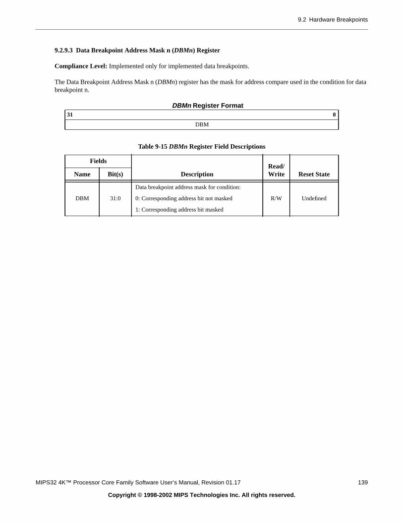
9.2 Hardware Breakpoints
data
9.2.9.3 Data Breakpoint Address Mask n (DBMn) Register
Compliance Level: Implemented only for implemented data breakpoints.
The Data Breakpoint Address Mask n (DBMn) register has the mask for address compare used in the condition forbreakpoint n.
DBMn Register Format31 0
DBM
Table 9-15DBMn Register Field Descriptions
Fields
DescriptionRead/Write Reset StateName Bit(s)
DBM 31:0
Data breakpoint address mask for condition:
0: Corresponding address bit not masked
1: Corresponding address bit masked
R/W Undefined
MIPS32 4K™ Processor Core Family Software User’s Manual, Revision 01.17 139
Copyright © 1998-2002 MIPS Technologies Inc. All rights reserved.
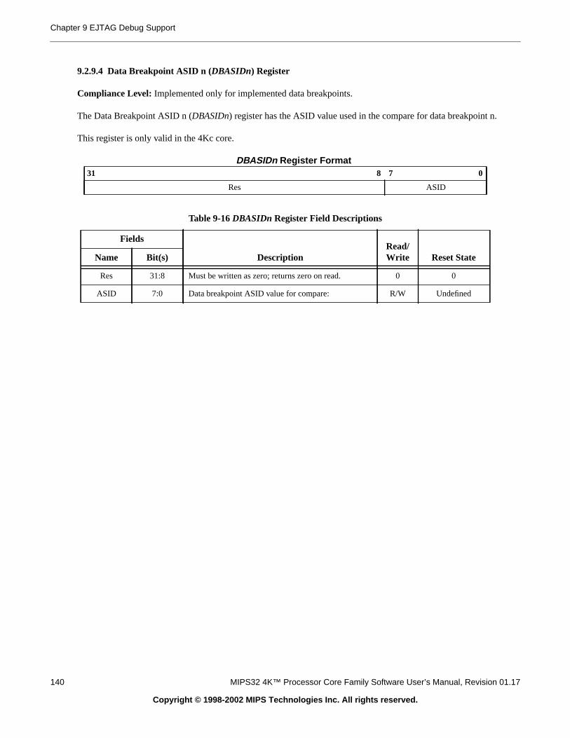
Chapter 9 EJTAG Debug Support
9.2.9.4 Data Breakpoint ASID n (DBASIDn) Register
Compliance Level: Implemented only for implemented data breakpoints.
The Data Breakpoint ASID n (DBASIDn) register has the ASID value used in the compare for data breakpoint n.
This register is only valid in the 4Kc core.
DBASIDn Register Format31 8 7 0
Res ASID
Table 9-16DBASIDn Register Field Descriptions
Fields
DescriptionRead/Write Reset StateName Bit(s)
Res 31:8 Must be written as zero; returns zero on read. 0 0
ASID 7:0 Data breakpoint ASID value for compare: R/W Undefined
140 MIPS32 4K™ Processor Core Family Software User’s Manual, Revision 01.17
Copyright © 1998-2002 MIPS Technologies Inc. All rights reserved.
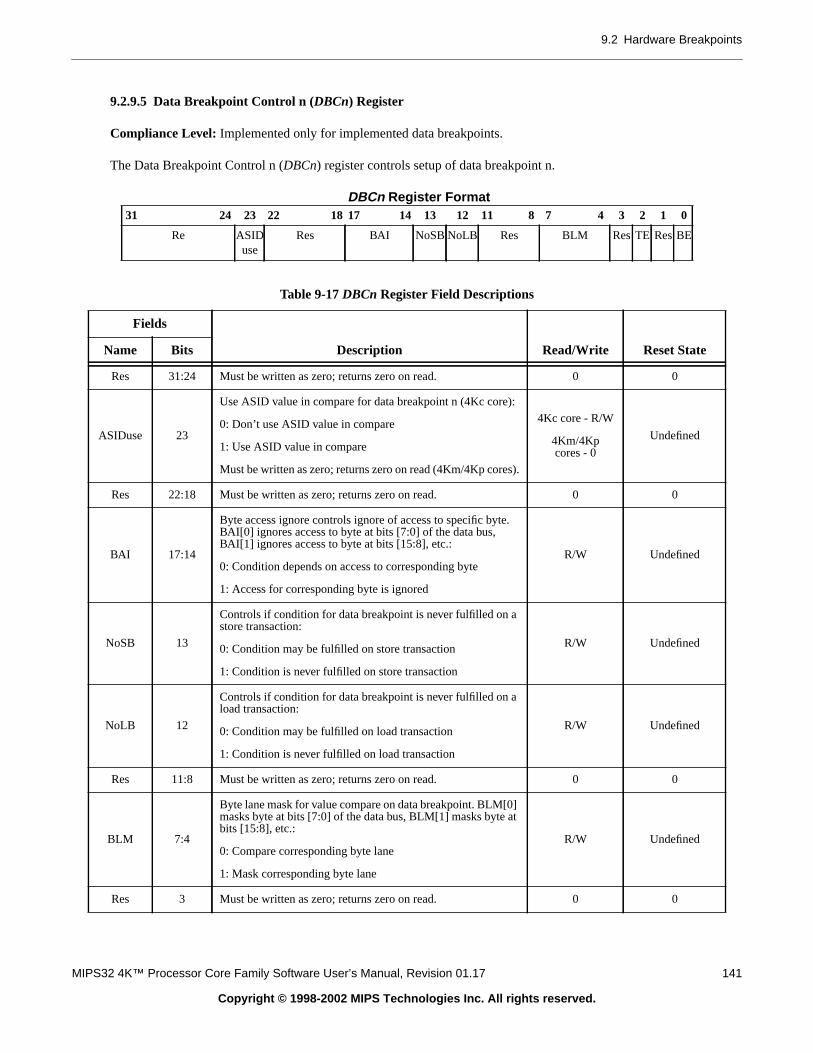
9.2 Hardware Breakpoints
9.2.9.5 Data Breakpoint Control n (DBCn) Register
Compliance Level: Implemented only for implemented data breakpoints.
The Data Breakpoint Control n (DBCn) register controls setup of data breakpoint n.
DBCn Register Format31 24 23 22 18 17 14 13 12 11 8 7 4 3 2 1 0
Re ASIDuse
Res BAI NoSB NoLB Res BLM Res TE Res BE
Table 9-17DBCn Register Field Descriptions
Fields
Description Read/Write Reset StateName Bits
Res 31:24 Must be written as zero; returns zero on read. 0 0
ASIDuse 23
Use ASID value in compare for data breakpoint n (4Kc core):
0: Don’t use ASID value in compare
1: Use ASID value in compare
Must be written as zero; returns zero on read (4Km/4Kp cores).
4Kc core - R/W
4Km/4Kpcores - 0
Undefined
Res 22:18 Must be written as zero; returns zero on read. 0 0
BAI 17:14
Byte access ignore controls ignore of access to specific byte.BAI[0] ignores access to byte at bits [7:0] of the data bus,BAI[1] ignores access to byte at bits [15:8], etc.:
0: Condition depends on access to corresponding byte
1: Access for corresponding byte is ignored
R/W Undefined
NoSB 13
Controls if condition for data breakpoint is never fulfilled on astore transaction:
0: Condition may be fulfilled on store transaction
1: Condition is never fulfilled on store transaction
R/W Undefined
NoLB 12
Controls if condition for data breakpoint is never fulfilled on aload transaction:
0: Condition may be fulfilled on load transaction
1: Condition is never fulfilled on load transaction
R/W Undefined
Res 11:8 Must be written as zero; returns zero on read. 0 0
BLM 7:4
Byte lane mask for value compare on data breakpoint. BLM[0]masks byte at bits [7:0] of the data bus, BLM[1] masks byte atbits [15:8], etc.:
0: Compare corresponding byte lane
1: Mask corresponding byte lane
R/W Undefined
Res 3 Must be written as zero; returns zero on read. 0 0
MIPS32 4K™ Processor Core Family Software User’s Manual, Revision 01.17 141
Copyright © 1998-2002 MIPS Technologies Inc. All rights reserved.

Chapter 9 EJTAG Debug Support
TE 2
Use data breakpoint n as triggerpoint:
0: Don’t use it as triggerpoint
1: Use it as triggerpoint
R/W 0
Res 1 Must be written as zero; returns zero on read. 0 0
BE 0
Use data breakpoint n as breakpoint:
0: Don’t use it as breakpoint
1: Use it as breakpoint
R/W 0
Table 9-17DBCn Register Field Descriptions (Continued)
Fields
Description Read/Write Reset StateName Bits
142 MIPS32 4K™ Processor Core Family Software User’s Manual, Revision 01.17
Copyright © 1998-2002 MIPS Technologies Inc. All rights reserved.

9.2 Hardware Breakpoints
9.2.9.6 Data Breakpoint Value n (DBVn) Register
Compliance Level: Implemented only for implemented data breakpoints.
The Data Breakpoint Value n (DBVn) register has the value used in the condition for data breakpoint n.
DBVn Register Format31 0
DBV
Table 9-18DBVn Register Field Descriptions
Fields
DescriptionRead/Write Reset StateName Bit(s)
DBV 31:0 Data breakpoint value for condition R/W Undefined
MIPS32 4K™ Processor Core Family Software User’s Manual, Revision 01.17 143
Copyright © 1998-2002 MIPS Technologies Inc. All rights reserved.

Chapter 9 EJTAG Debug Support
hievedebug
9.3 Test Access Port (TAP)
The following main features are supported by the TAP module:
• 5-pin industry standard JTAG Test Access Port (TCK, TMS, TDI, TDO, TRST_N) interface, which is compatible withIEEE Std. 1149.1.
• Target chip and EJTAG feature identification available through the Test Access Port (TAP) controller.
• The processor can access external memory on the EJTAG Probe serially through the EJTAG pins. This is acthrough so-called Processor Access (PA), and is used to eliminate the use of the user’s system memory for droutines.
• Support for both ROM based debugger and debugging both through TAP.
9.3.1 EJTAG Internal and External Interfaces
The external interface of the EJTAG Module consists of the 5 signals defined by the IEEE standard.
Table 9-19 EJTAG Interface Pins
Pin Type Description
TCK I
Test Clock Input
Input clock used to shift data into or out of the Instruction or dataregisters. TheTCK clock is independent of the processor clock, so theEJTAG probe can driveTCK independently of the processor clockfrequency.
The core signal for this is calledEJ_TCK
TMS I
Test Mode Select Input
TheTMS input signal is decoded by the TAP controller to control testoperation.TMS is sampled on the rising edge ofTCK.
The core signal for this is calledEJ_TMS
TDI I
Test Data Input
Serial input data (TDI) is shifted into the Instruction register or dataregisters on the rising edge of theTCK clock, depending on the TAPcontroller state.
The core signal for this is calledEJ_TDI
TDO O
Test Data Output
Serial output data is shifted from the Instruction or data register to theTDOpin at the falling edge of theTCKclock. When no data is shifted out,theTDO is 3-stated.
The core signal for this is calledEJ_TDO with output enable control byEJ_TDOzstate.
144 MIPS32 4K™ Processor Core Family Software User’s Manual, Revision 01.17
Copyright © 1998-2002 MIPS Technologies Inc. All rights reserved.

9.3 Test Access Port (TAP)
mall
theegisters,ction
lowing
ataPause
to holdot output
9.3.2 Test Access Port Operation
The TAP controller is controlled by the Test Clock (TCK) and Test Mode Select (TMS) inputs. These two inputsdetermine whether an the Instruction register scan or data register scan is performed. The TAP consists of a scontroller, driven by theTCK input, which responds to theTMSinput as shown in the state diagram inFigure 9-5. TheTAP uses both clock edges ofTCK. TMS andTDI are sampled on the rising edge ofTCK, whileTDO changes on thefalling edge ofTCK.
At power-up the TAP is forced into theTest-Logic-Reset either by low value onTRST_N. The TAP instruction registeris thereby reset to IDCODE. No other parts of the EJTAG hardware are reset through theTest-Logic-Reset state.
When test access is required, a protocol is applied via theTMS andTCK inputs, causing the TAP to exit theTest-Logic-Resetstate and move through the appropriate states. From theRun-Test/Idlestate, an Instruction register scanor a data register scan can be issued to transition the TAP through the appropriate states shown inFigure 9-5.
The states of the data and instruction register scan blocks are mirror images of each other adding symmetry toprotocol sequences. The first action that occurs when either block is entered is a capture operation. For the data rtheCapture-DR state is used to capture (or parallel load) the data into the selected serial data path. In the Instruregister, theCapture-IR state is used to capture status information into the Instruction register.
From theCapture states, the TAP transitions to either theShift or Exit1 states. Normally theShift state follows theCapturestate so that test data or status information can be shifted out for inspection and new data shifted in. FoltheShiftstate, the TAP either returns to theRun-Test/Idlestate via theExit1andUpdatestates or enters thePausestatevia Exit1. The reason for entering thePause state is to temporarily suspend the shifting of data through either the Dor Instruction Register while a required operation, such as refilling a host memory buffer, is performed. From thestate shifting can resume by re-entering theShiftstate via theExit2state or terminated by entering theRun-Test/Idlestatevia theExit2 andUpdate states.
Upon entering the data or Instruction register scan blocks, shadow latches in the selected scan path are forcedtheir present state during the Capture and Shift operations. The data being shifted into the selected scan path is nthrough the shadow latch until the TAP enters theUpdate-DR or Update-IR state. TheUpdate state causes the shadowlatches to update (or parallel load) with the new data that has been shifted into the selected scan path.
TRST_N I
Test Reset Input (Optional pin)
TheTRST_N pin is an active-low signal for asynchronous reset of theTAP controller and instruction in the TAP module, independent of theprocessor logic. The processor is not reset by the assertion ofTRST_N.
The core signal for this is calledEJ_TRST_N
This signal is optional, but power-on reset must apply a low pulse on thisis signal at power-on and then leave it high, in case the signal is notavailable as a pin on the chip. If available on the chip, then it must be lowon the board when the EJTAG debug features are unused by the probe.
Table 9-19 EJTAG Interface Pins (Continued)
Pin Type Description
MIPS32 4K™ Processor Core Family Software User’s Manual, Revision 01.17 145
Copyright © 1998-2002 MIPS Technologies Inc. All rights reserved.

Chapter 9 EJTAG Debug Support
change
evious
is
evious
Figure 9-5 TAP Controller State Diagram
9.3.2.1 Test-Logic-Reset State
In theTest-Logic-Reset state the boundary scan test logic is disabled. The test logic enters theTest-Logic-Reset statewhen theTMS input is held HIGH for at least five rising edges ofTCK. The BYPASS instruction is forced into theinstruction register output latches during this state. The controller remains in theTest-Logic-Resetstate as long asTMSis HIGH.
9.3.2.2 Run-Test/Idle State
The controller enters theRun-Test/Idlestate between scan operations. The controller remains in this state as long asTMSis held LOW. The instruction register and all test data registers retain their previous state. The instruction cannotwhen the TAP controller is in this state.
WhenTMS is sampled HIGH at the rising edge ofTCK, the controller transitions to theSelect_DR state.
9.3.2.3 Select_DR_Scan State
This is a temporary controller state in which all test data registers selected by the current instruction retain their prstate. IfTMSis sampled LOW at the rising edge ofTCK, the controller transitions to theCapture_DRstate. A HIGH onTMScauses the controller to transition to theSelect_IRstate. The instruction cannot change while the TAP controllerin this state.
9.3.2.4 Select_IR_Scan State
This is a temporary controller state in which all test data registers selected by the current instruction retain their prstate. IfTMSis sampled LOW at the rising edge ofTCK, the controller transitions to theCapture_IRstate. A HIGH onTMS causes the controller to transition to theTest-Reset-Logic state. The instruction cannot change while the TAPcontroller is in this state.
Shift_IR
Select_IR_Scan
Capture_IR
Exit1_IR
Pause_IR
Exit2_IR
Update_IR
1
0
0
0
0
0
0
1
1
1
1
1
1
1
0
Shift_DR
Select_DR_Scan
Capture_DR
Exit1_DR
Pause_DR
Exit2_DR
Update_DR
0
0
0
0
0
0
1
1
1
1
1
1
1
0
Test-Logic-Reset
Run-Test/Idle
0
1
0
146 MIPS32 4K™ Processor Core Family Software User’s Manual, Revision 01.17
Copyright © 1998-2002 MIPS Technologies Inc. All rights reserved.
9.3 Test Access Port (TAP)
the value
e
evious
ion
serial
e.
evious
f
errevious
te.
9.3.2.5 Capture_DR State
In this state the boundary scan register captures value of the register addressed by the Instruction register, andis then shifted out in theShift_DR. If TMS is sampled LOW at the rising edge ofTCK, the controller transitions to theShift_DRstate. A HIGH onTMScauses the controller to transition to theExit1_DRstate. The instruction cannot changewhile the TAP controller is in this state.
9.3.2.6 Shift_DR State
In this state the test data register connected betweenTDI andTDO as a result of the current instruction shifts data onstage toward its serial output on the rising edge ofTCK. If TMSis sampled LOW at the rising edge ofTCK, the controllerremains in theShift_DRstate. A HIGH onTMScauses the controller to transition to theExit1_DRstate. The instructioncannot change while the TAP controller is in this state.
9.3.2.7 Exit1_DR State
This is a temporary controller state in which all test data registers selected by the current instruction retain their prstate. IfTMS is sampled LOW at the rising edge ofTCK, the controller transitions to thePause_DR state. A HIGH onTMS causes the controller to transition to theUpdate_DR state which terminates the scanning process. The instructcannot change while the TAP controller is in this state.
9.3.2.8 Pause_DR State
ThePause_DRstate allows the controller to temporarily halt the shifting of data through the test data register in thepath betweenTDI andTDO. All test data registers selected by the current instruction retain their previous state. IfTMSis sampled LOW at the rising edge ofTCK, the controller remains in thePause_DR state. A HIGH onTMS causes thecontroller to transition to theExit2_DR state. The instruction cannot change while the TAP controller is in this stat
9.3.2.9 Exit2_DR State
This is a temporary controller state in which all test data registers selected by the current instruction retain their prstate. IfTMSis sampled LOW at the rising edge ofTCK, the controller transitions to theShift_DRstate to allow anotherserial shift of data. A HIGH onTMS causes the controller to transition to theUpdate_DR state which terminates thescanning process. The instruction cannot change while the TAP controller is in this state.
9.3.2.10 Update_DR State
When the TAP controller is in this state the value shifted in during theShift_DR state takes effect at the rising edge otheTCK for the register indicated by the Instruction register.
If TMSis sampled LOW at the rising edge ofTCK, the controller transitions to theRun-Test/Idlestate. A HIGH onTMScauses the controller to transition to theSelect_DR_Scanstate. The instruction cannot change while the TAP controllis in this state and all shift register stages in the test data registers selected by the current instruction retain their pstate.
9.3.2.11 Capture_IR State
In this state the shift register contained in the Instruction register loads a fixed pattern (000012) on the rising edge ofTCK. The data registers selected by the current instruction retain their previous state.
If TMSis sampled LOW at the rising edge ofTCK, the controller transitions to theShift_IRstate. A HIGH onTMScausesthe controller to transition to theExit1_IRstate. The instruction cannot change while the TAP controller is in this sta
MIPS32 4K™ Processor Core Family Software User’s Manual, Revision 01.17 147
Copyright © 1998-2002 MIPS Technologies Inc. All rights reserved.
Chapter 9 EJTAG Debug Support
ut
r is in
the
on
en
9.3.2.12 Shift_IR State
In this state the instruction register is connected betweenTDI andTDOand shifts data one stage toward its serial outpon the rising edge ofTCK. If TMSis sampled LOW at the rising edge ofTCK, the controller remains in theShift_IRstate.A HIGH onTMS causes the controller to transition to theExit1_IR state.
9.3.2.13 Exit1_IR State
This is a temporary controller state in which all registers retain their previous state. IfTMSis sampled LOW at the risingedge ofTCK, the controller transitions to thePause_IRstate. A HIGH onTMScauses the controller to transition to theUpdate_IR state which terminates the scanning process. The instruction cannot change while the TAP controllethis state and the instruction register retains its previous state.
9.3.2.14 Pause_IR State
ThePause_IR state allows the controller to temporarily halt the shifting of data through the instruction register inserial path betweenTDI andTDO. If TMS is sampled LOW at the rising edge ofTCK, the controller remains in thePause_IRstate. A HIGH onTMScauses the controller to transition to theExit2_IRstate. The instruction cannot changewhile the TAP controller is in this state.
9.3.2.15 Exit2_IR State
This is a temporary controller state in which the instruction register retains its previous state. IfTMS is sampled LOWat the rising edge ofTCK, the controller transitions to theShift_IRstate to allow another serial shift of data. A HIGH onTMS causes the controller to transition to theUpdate_IR state which terminates the scanning process. The instructicannot change while the TAP controller is in this state.
9.3.2.16 Update_IR State
The instruction shifted into the instruction register takes effect on the rising edge ofTCK.
If TMSis sampled LOW at the rising edge ofTCK, the controller transitions to theRun-Test/Idlestate. A HIGH onTMScauses the controller to transition to theSelect_DR_Scan state.
9.3.3 Test Access Port (TAP) Instructions
The TAP Instruction register allows instructions to be serially input into the device when TAP controller is in theShift-IRstate. Instructions are decoded and define the serial test data register path that is used to shift data betweenTDI andTDOduring data register scanning.
The Instruction register is a 5-bit register. In the current EJTAG implementation only some instructions have bedecoded; the unused instructions are set default to the BYPASS instruction.
Table 9-20 Implemented EJTAG Instructions
Value Instruction Function
0x01 IDCODE Select Chip Identification data register
0x03 IMPCODE Select Implementation Register
0x08 ADDRESS Select Address register
0x09 DATA Select Data register
148 MIPS32 4K™ Processor Core Family Software User’s Manual, Revision 01.17
Copyright © 1998-2002 MIPS Technologies Inc. All rights reserved.

9.3 Test Access Port (TAP)
ister tossorEEE
gisterngth thescan
gisterany
9.3.3.1 BYPASS Instruction
The required BYPASS instruction allows the processor to remain in a functional mode and selects the Bypass regbe connected betweenTDI andTDO. The BYPASS instruction allows serial data to be transferred through the procefrom TDI to TDO without affecting its operation. The bit code of this instruction is defined to be all ones by the I1149.1 standard. Any unused instruction is defaulted to the BYPASS instruction.
9.3.3.2 IDCODE Instruction
The IDCODE instruction allows the processor in its functional mode and selects the Device Identification (ID) reto be connected betweenTDI andTDO. The Device ID register is a 32-bit shift register containing information regardithe IC manufacturer, device type, and version code. Accessing the Identification Register does not interfere wioperation of the processor. Also, access to the Identification Register is immediately available, via a TAP data operation, after power-up when the TAP has been reset with on-chip power-on or through the optionalTRST_N pin.
9.3.3.3 IMPCODE Instruction
This instruction selects the Implementation register for output, which is always 32 bits.
9.3.3.4 ADDRESS Instruction
This instruction is used to select the Address register to be connected betweenTDI andTDO. The EJTAG Probe shifts32 bits through theTDI pin into the Address register and shifts out the captured address via theTDO pin.
9.3.3.5 DATA Instruction
This instruction is used to select the Data register to be connected betweenTDI andTDO. The EJTAG Probe shifts 32bits ofTDI data into the Data register and shifts out the captured data via theTDO pin.
9.3.3.6 CONTROL Instruction
This instruction is used to select the EJTAG Control register to be connected betweenTDI andTDO. The EJTAG Probeshifts 32 bits ofTDI data into the EJTAG Control register and shifts out the EJTAG Control register bits viaTDO.
9.3.3.7 ALL Instruction
This instruction is used to select the concatenation of the Address and Data register, and the EJTAG Control rebetweenTDI andTDO. It can be used in particular if switching instructions in the instruction register takes too mTCK cycles. The first bit shifted out is bit 0.
0x0A CONTROL Select EJTAG Control register
0x0B ALL Select the Address, Data and EJTAG Control registers
0x0C EJTAGBOOT Set EjtagBrk, ProbEn and ProbTrap to 1 as reset value
0x0D NORMALBOOT Set EjtagBrk, ProbEn and ProbTrap to 0 as reset value
0x0E FASTDATA Selects the Data and Fastdata registers
0x1F BYPASS Bypass mode
Table 9-20 Implemented EJTAG Instructions
Value Instruction Function
MIPS32 4K™ Processor Core Family Software User’s Manual, Revision 01.17 149
Copyright © 1998-2002 MIPS Technologies Inc. All rights reserved.
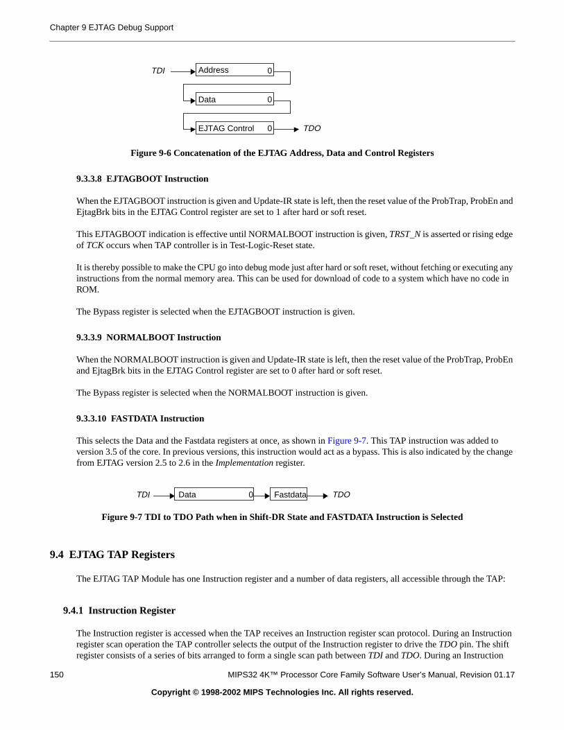
Chapter 9 EJTAG Debug Support
En and
ng anycode in
robEn
change
TAP:
truction
Figure 9-6 Concatenation of the EJTAG Address, Data and Control Registers
9.3.3.8 EJTAGBOOT Instruction
When the EJTAGBOOT instruction is given and Update-IR state is left, then the reset value of the ProbTrap, ProbEjtagBrk bits in the EJTAG Control register are set to 1 after hard or soft reset.
This EJTAGBOOT indication is effective until NORMALBOOT instruction is given,TRST_Nis asserted or rising edgeof TCK occurs when TAP controller is in Test-Logic-Reset state.
It is thereby possible to make the CPU go into debug mode just after hard or soft reset, without fetching or executiinstructions from the normal memory area. This can be used for download of code to a system which have no ROM.
The Bypass register is selected when the EJTAGBOOT instruction is given.
9.3.3.9 NORMALBOOT Instruction
When the NORMALBOOT instruction is given and Update-IR state is left, then the reset value of the ProbTrap, Pand EjtagBrk bits in the EJTAG Control register are set to 0 after hard or soft reset.
The Bypass register is selected when the NORMALBOOT instruction is given.
9.3.3.10 FASTDATA Instruction
This selects the Data and the Fastdata registers at once, as shown inFigure 9-7. This TAP instruction was added toversion 3.5 of the core. In previous versions, this instruction would act as a bypass. This is also indicated by thefrom EJTAG version 2.5 to 2.6 in theImplementation register.
Figure 9-7 TDI to TDO Path when in Shift-DR State and FASTDATA Instruction is Selected
9.4 EJTAG TAP Registers
The EJTAG TAP Module has one Instruction register and a number of data registers, all accessible through the
9.4.1 Instruction Register
The Instruction register is accessed when the TAP receives an Instruction register scan protocol. During an Insregister scan operation the TAP controller selects the output of the Instruction register to drive theTDO pin. The shiftregister consists of a series of bits arranged to form a single scan path betweenTDI andTDO. During an Instruction
Address 0
Data 0
EJTAG Control 0 TDO
TDI
TDI Data TDOFastdata0
150 MIPS32 4K™ Processor Core Family Software User’s Manual, Revision 01.17
Copyright © 1998-2002 MIPS Technologies Inc. All rights reserved.
9.4 EJTAG TAP Registers
ion. A
g a dataol signalsput
bit scanolvedisfy the
sion,
f theruction.
register scan operations, the TAP controls the register to capture status information and shift data fromTDI toTDO. Boththe capture and shift operations occur on the rising edge ofTCK. However, the data shifted out from theTDOoccurs onthe falling edge ofTCK. In the Test-Logic-Reset andCapture-IR state, the instruction shift register is set to 000012, asfor IDCODE instruction. This forces the device into the functional mode and selects the Device ID register. TheInstruction register is 5 bits wide. The instruction shifted in takes effect for the following data register scan operatlist of the implemented instructions are listed inTable 9-20 on page 148.
9.4.2 Data Registers Overview
The EJTAG uses several data registers, which are arranged in parallel from the primaryTDI input to the primaryTDOoutput. The Instruction register supplies the address that allows one of the data registers to be accessed durinregister scan operation. During a data register scan operation, the addressed scan register receives TAP contrto capture the register and shift data fromTDI to TDO. During a data register scan operation, the TAP selects the outof the data register to drive theTDO pin. The register is updated in theUpdate-DR state with respect to write bits.
This description applies in general to the following data registers:
• Bypass Register
• Device Identification Register
• Implementation Register
• EJTAG Control Register (ECR)
• Processor Access Address Register
• Processor Access Data Register
• FastData Register
9.4.2.1 Bypass Register
TheBypass register consists of a single scan register bit. When selected, the Bypass register provides a single path betweenTDI andTDO. The Bypass register allows abbreviating the scan path through devices that are not invin the test. The Bypass register is selected when the Instruction register is loaded with a pattern of all ones to satIEEE 1149.1 Bypass instruction requirement.
9.4.2.2 Device Identification (ID ) Register
TheDevice Identificationregister is defined by IEEE 1149.1, to identify the device's manufacturer, part number, reviand other device-specific information.Table 9-21 shows the bit assignments defined for the read-only DeviceIdentification Register, and inputs to the core determine the value of these bits. These bits can be scanned out oIDregister after being selected. The register is selected when the Instruction register is loaded with the IDCODE inst
Device Identification Register Format31 28 27 12 11 1 0
Version PartNumber ManufID R
MIPS32 4K™ Processor Core Family Software User’s Manual, Revision 01.17 151
Copyright © 1998-2002 MIPS Technologies Inc. All rights reserved.

Chapter 9 EJTAG Debug Support
lue aretruction.
9.4.2.3 Implementation Register
This 32-bit read-only register is used to identify the features of the EJTAG implementation. Some of the reset vaset by inputs to the core.The register is selected when the Instruction register is loaded with the IMPCODE ins
Implementation Register Format
Table 9-21 Device Identification Register
Fields
DescriptionRead/Write Reset StateName Bit(s)
Version 31:28
Version (4 bits)
This field identifies the version number of theprocessor derivative.
R EJ_Version[3:0]
PartNumber 27:12
Part Number (16 bits)
This field identifies the part number of the processorderivative.
R EJ_PartNumber[15:0]
ManufID 11:1
Manufacturer Identity (11 bits)
Accordingly to IEEE 1149.1-1990, the manufactureridentity code shall be a compressed form of theJEDEC Publications 106-A.
R EJ_ManufID[10:0]
R 0 reserved R 1
31 29 28 25 24 23 21 20 15 14 13 0
EJTAGver reserved DINTsup ASIDsize reserved NoDMA reserved
Table 9-22Implementation Register Descriptions
Fields
DescriptionRead/Write Reset StateName Bit(s)
EJTAGver 31:29
EJTAG Version
1: Version 2.5 (core revisions before 3.5)
2: Version 2.6 (core revisions 3.5 and later)
R Preset
reserved 28:25 reserved R 0
DINTsup 24
DINT Signal Supported from Probe
This bit indicates if the DINT signal from the probe issupported:
0: DINT signal from the probe is not supported1: Probe can use DINT signal to make debug interrupt.
R EJ_DINTsup
ASIDsize 23:21
Size of ASID field in implementation:
0: No ASID in implementation (4Km/4Kp cores)1: 6-bit ASID2: 8-bit ASID (4Kc core)3: Reserved
R
4Kc core - 2
4Km/4Kpcores - 0
reserved 20:15 reserved R 0
NoDMA 14 No EJTAG DMA Support R 1
152 MIPS32 4K™ Processor Core Family Software User’s Manual, Revision 01.17
Copyright © 1998-2002 MIPS Technologies Inc. All rights reserved.

9.4 EJTAG TAP Registers
heifting
r 0
APstillet
9.4.2.4 EJTAG Control Register
This 32-bit register controls the various operations of the TAP modules. This register is selected by shifting in tCONTROL instruction. Bits in the EJTAG Control register can be set/cleared by shifting in data; status is read by shout the contents of this register. This EJTAG Control register can only be accessed by the TAP interface.
The EJTAG Control register is not updated in theUpdate-DR state unless the Reset occurred (Rocc), bit 31, is eitheor written to 0. This is in order to ensure prober handling of processor accesses.
The value used for reset indicated in the table below takes effect on both hard and soft CPU reset, but no on Tcontroller reset by e.g.TRST_N. TCKclock is not required when the hard or soft CPU reset occurs, but the bits areupdated to the reset value when theTCKapplies. The first 5TCKclocks after hard or soft CPU reset may result in resof the bits, due to synchronization between clock domains.
EJTAG Control Register Format
reserved 13:0 reserved R 0
31 30 29 28 23 22 21 20 19 18 17 16 15 14 13 12 11 4 3 2 0
Rocc Psz Res Doze Halt PerRst PRnW PrAcc Res PrRst ProbEn ProbTrap Res EjtagBrk Res DM Res
Table 9-23EJTAG Control Register Descriptions
Fields
DescriptionRead/Write Reset StateName Bit(s)
Rocc 31
Reset Occurred
The bit indicates if hard or soft reset has occurred:0: No reset occurred since bit last cleared.1: Reset occurred since bit last cleared.
The Rocc bit will keep the 1 value as long as hard or softreset is applied.
This bit must be cleared by the probe, to acknowledgethat the incident was detected.
The EJTAG Control register is not updated in theUpdate-DRstate unless Rocc is 0, or written to 0. This isin order to ensure prober handling of processor access.
R/W 1
Table 9-22Implementation Register Descriptions
Fields
DescriptionRead/Write Reset StateName Bit(s)
MIPS32 4K™ Processor Core Family Software User’s Manual, Revision 01.17 153
Copyright © 1998-2002 MIPS Technologies Inc. All rights reserved.
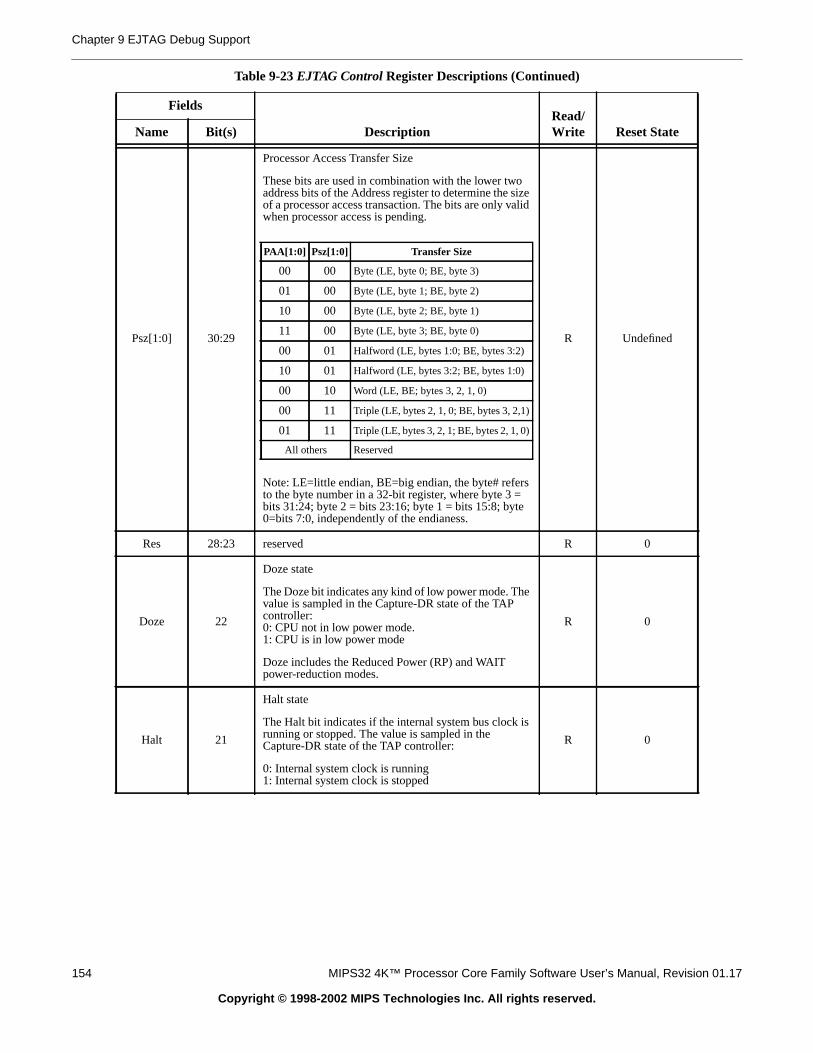
Chapter 9 EJTAG Debug Support
Psz[1:0] 30:29
Processor Access Transfer Size
These bits are used in combination with the lower twoaddress bits of the Address register to determine the sizeof a processor access transaction. The bits are only validwhen processor access is pending.
Note: LE=little endian, BE=big endian, the byte# refersto the byte number in a 32-bit register, where byte 3 =bits 31:24; byte 2 = bits 23:16; byte 1 = bits 15:8; byte0=bits 7:0, independently of the endianess.
R Undefined
Res 28:23 reserved R 0
Doze 22
Doze state
The Doze bit indicates any kind of low power mode. Thevalue is sampled in the Capture-DR state of the TAPcontroller:0: CPU not in low power mode.1: CPU is in low power mode
Doze includes the Reduced Power (RP) and WAITpower-reduction modes.
R 0
Halt 21
Halt state
The Halt bit indicates if the internal system bus clock isrunning or stopped. The value is sampled in theCapture-DR state of the TAP controller:
0: Internal system clock is running1: Internal system clock is stopped
R 0
Table 9-23EJTAG Control Register Descriptions (Continued)
Fields
DescriptionRead/Write Reset StateName Bit(s)
PAA[1:0] Psz[1:0] Transfer Size
00 00 Byte (LE, byte 0; BE, byte 3)
01 00 Byte (LE, byte 1; BE, byte 2)
10 00 Byte (LE, byte 2; BE, byte 1)
11 00 Byte (LE, byte 3; BE, byte 0)
00 01 Halfword (LE, bytes 1:0; BE, bytes 3:2)
10 01 Halfword (LE, bytes 3:2; BE, bytes 1:0)
00 10 Word (LE, BE; bytes 3, 2, 1, 0)
00 11 Triple (LE, bytes 2, 1, 0; BE, bytes 3, 2,1)
01 11 Triple (LE, bytes 3, 2, 1; BE, bytes 2, 1, 0)
All others Reserved
154 MIPS32 4K™ Processor Core Family Software User’s Manual, Revision 01.17
Copyright © 1998-2002 MIPS Technologies Inc. All rights reserved.
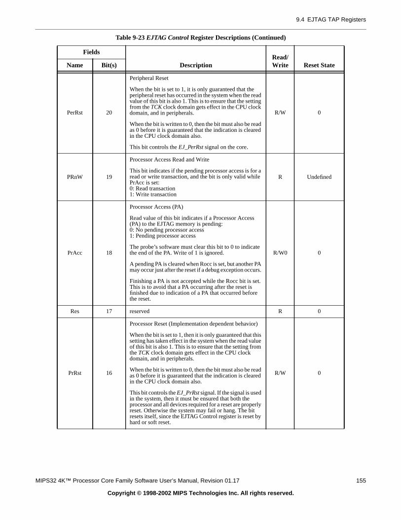
9.4 EJTAG TAP Registers
PerRst 20
Peripheral Reset
When the bit is set to 1, it is only guaranteed that theperipheral reset has occurred in the system when the readvalue of this bit is also 1. This is to ensure that the settingfrom theTCKclock domain gets effect in the CPU clockdomain, and in peripherals.
When the bit is written to 0, then the bit must also be readas 0 before it is guaranteed that the indication is clearedin the CPU clock domain also.
This bit controls theEJ_PerRst signal on the core.
R/W 0
PRnW 19
Processor Access Read and Write
This bit indicates if the pending processor access is for aread or write transaction, and the bit is only valid whilePrAcc is set:0: Read transaction1: Write transaction
R Undefined
PrAcc 18
Processor Access (PA)
Read value of this bit indicates if a Processor Access(PA) to the EJTAG memory is pending:0: No pending processor access1: Pending processor access
The probe’s software must clear this bit to 0 to indicatethe end of the PA. Write of 1 is ignored.
A pending PA is cleared when Rocc is set, but another PAmay occur just after the reset if a debug exception occurs.
Finishing a PA is not accepted while the Rocc bit is set.This is to avoid that a PA occurring after the reset isfinished due to indication of a PA that occurred beforethe reset.
R/W0 0
Res 17 reserved R 0
PrRst 16
Processor Reset (Implementation dependent behavior)
When the bit is set to 1, then it is only guaranteed that thissetting has taken effect in the system when the read valueof this bit is also 1. This is to ensure that the setting fromtheTCK clock domain gets effect in the CPU clockdomain, and in peripherals.
When the bit is written to 0, then the bit must also be readas 0 before it is guaranteed that the indication is clearedin the CPU clock domain also.
This bit controls theEJ_PrRstsignal. If the signal is usedin the system, then it must be ensured that both theprocessor and all devices required for a reset are properlyreset. Otherwise the system may fail or hang. The bitresets itself, since the EJTAG Control register is reset byhard or soft reset.
R/W 0
Table 9-23EJTAG Control Register Descriptions (Continued)
Fields
DescriptionRead/Write Reset StateName Bit(s)
MIPS32 4K™ Processor Core Family Software User’s Manual, Revision 01.17 155
Copyright © 1998-2002 MIPS Technologies Inc. All rights reserved.

Chapter 9 EJTAG Debug Support
ProbEn 15
Probe Enable
This bit indicates to the CPU if the EJTAG memory ishandled by the probe so processor accesses areanswered:0: The probe does not handle EJTAG memorytransactions1: The probe does handle EJTAG memory transactions
It is an error by the software controlling the probe if itsets the ProbTrap to 1 but the ProbEn to 0. The operationof the processor is UNDEFINED in this case.
The ProbEn bit is reflected as a read-only bit in theProbEn bit, bit 0, in the Debug Control Register (DCR).
The read value indicates the effective value in the DCR,due to synchronization issues betweenTCK and CPUclock domains. However, it is ensured that change of theProbEn prior to setting the EjtagBrk bit will have effectfor the debug handler executed due to the debugexception.
The reset value of the bit depends on whether theEJTAGBOOT indication is given or not:No EJTAGBOOT indication given: 0EJTAGBOOT indication given: 1
R/W
0 or 1
from
EJTAGBOOT
ProbTrap 14
Probe Trap
This bit controls the location of the debug exceptionvector:0: In normal memory 0xBFC0.04801: In EJTAG memory at 0xFF20.0200 in dmseg
Valid setting of the ProbTrap bit depends on the settingof the ProbEn bit, see comment under ProbEn bit.
The ProbTrap should not be set to 1, for debug exceptionvector in EJTAG memory, unless the ProbEn bit is alsoset to 1 to indicate that the EJTAG memory may beaccessed.
The read value indicates the effective value to the CPU,due to synchronization issues betweenTCK and CPUclock domains. However, it is ensured that change of theProbTrap prior to setting the EjtagBrk bit will have effectfor the EjtagBrk.
The reset value of the bit depends on whether theEJTAGBOOT indication is given or not:No EJTAGBOOT indication given: 0EJTAGBOOT indication given: 1
R/W
0 or 1
from
EJTAGBOOT
Res 13 reserved R 0
Table 9-23EJTAG Control Register Descriptions (Continued)
Fields
DescriptionRead/Write Reset StateName Bit(s)
156 MIPS32 4K™ Processor Core Family Software User’s Manual, Revision 01.17
Copyright © 1998-2002 MIPS Technologies Inc. All rights reserved.
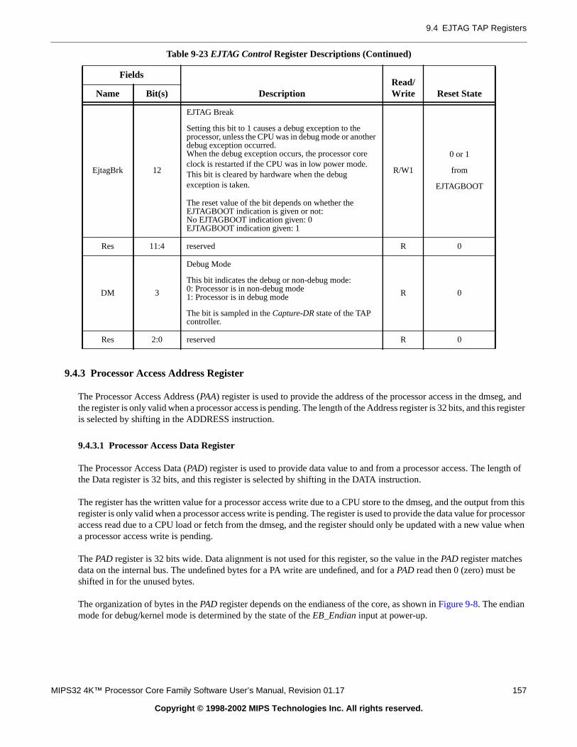
9.4 EJTAG TAP Registers
g, andregister
th of
rom thisocessore when
9.4.3 Processor Access Address Register
The Processor Access Address (PAA) register is used to provide the address of the processor access in the dmsethe register is only valid when a processor access is pending. The length of the Address register is 32 bits, and thisis selected by shifting in the ADDRESS instruction.
9.4.3.1 Processor Access Data Register
The Processor Access Data (PAD) register is used to provide data value to and from a processor access. The lengthe Data register is 32 bits, and this register is selected by shifting in the DATA instruction.
The register has the written value for a processor access write due to a CPU store to the dmseg, and the output fregister is only valid when a processor access write is pending. The register is used to provide the data value for praccess read due to a CPU load or fetch from the dmseg, and the register should only be updated with a new valua processor access write is pending.
ThePAD register is 32 bits wide. Data alignment is not used for this register, so the value in thePAD register matchesdata on the internal bus. The undefined bytes for a PA write are undefined, and for aPAD read then 0 (zero) must beshifted in for the unused bytes.
The organization of bytes in thePAD register depends on the endianess of the core, as shown inFigure 9-8. The endianmode for debug/kernel mode is determined by the state of theEB_Endian input at power-up.
EjtagBrk 12
EJTAG Break
Setting this bit to 1 causes a debug exception to theprocessor, unless the CPU was in debug mode or anotherdebug exception occurred.When the debug exception occurs, the processor coreclock is restarted if the CPU was in low power mode.This bit is cleared by hardware when the debugexception is taken.
The reset value of the bit depends on whether theEJTAGBOOT indication is given or not:No EJTAGBOOT indication given: 0EJTAGBOOT indication given: 1
R/W1
0 or 1
from
EJTAGBOOT
Res 11:4 reserved R 0
DM 3
Debug Mode
This bit indicates the debug or non-debug mode:0: Processor is in non-debug mode1: Processor is in debug mode
The bit is sampled in theCapture-DR state of the TAPcontroller.
R 0
Res 2:0 reserved R 0
Table 9-23EJTAG Control Register Descriptions (Continued)
Fields
DescriptionRead/Write Reset StateName Bit(s)
MIPS32 4K™ Processor Core Family Software User’s Manual, Revision 01.17 157
Copyright © 1998-2002 MIPS Technologies Inc. All rights reserved.

Chapter 9 EJTAG Debug Support
., a bit isther thecess was
(on the. Aifies thee Data +
Figure 9-8 Endian Formats for thePAD Register
The size of the transaction and thus the number of bytes available/required for thePADregister is determined by the Pszfield in theECR.
9.4.4 Fastdata Register (TAP Instruction FASTDATA)
The width of the Fastdata register is 1 bit. During a Fastdata access, the Fastdata register is written and read, i.eshifted in and a bit is shifted out. During a Fastdata access, the Fastdata register value shifted in specifies wheFastdata access should be completed or not. The value shifted out is a flag that indicates whether the Fastdata acsuccessful or not (if completion was requested).
Fastdata Register Format
The FASTDATA access is used for efficient block transfers between dmseg (on the probe) and target memory processor). An “upload” is defined as a sequence of processor loads from target memory and stores to dmseg“download” is a sequence of processor loads from dmseg and stores to target memory. The “Fastdata area” speclegal range of dmseg addresses (0xFF20.0000 - 0xFF20.000F) that can be used for uploads and downloads. Th
0SPrAcc
Table 9-24 Fastdata Register Field Description
Fields
DescriptionRead/Write
Power-upStateName Bits
SPrAcc 0
Shifting in a zero value requests completion of theFastdata access. The PrAcc bit in the EJTAG Controlregister is overwritten with zero when the access succeeds.(The access succeeds if PrAcc is one and the operationaddress is in the legal dmseg Fastdata area.) Whensuccessful, a one is shifted out. Shifting out a zeroindicates a Fastdata access failure.
Shifting in a one does not complete the Fastdata accessand the PrAcc bit is unchanged. Shifting out a oneindicates that the access would have been successful ifallowed to complete and a zero indicates the access wouldnot have successfully completed.
R/W Undefined
A[n:0]=7 6 5 4
012A[n:0]=3
A[n:0]=4 5 6 7
321A[n:0]=0
0781516232431
0781516232431
LSBbit
MSB
LSBbit
MSB
A[n:2]=1
A[n:2]=0
A[n:2]=1
A[n:2]=0
Most significant byte is at lowest address.Word is addressed by byte address of most significant byte.
BIG-ENDIAN
LITTLE-ENDIAN
Least significant byte is at lowest address.Word is addressed by byte address of least significant byte.
158 MIPS32 4K™ Processor Core Family Software User’s Manual, Revision 01.17
Copyright © 1998-2002 MIPS Technologies Inc. All rights reserved.

9.5 Processor Accesses
a
rocessorccesses if theloads willa being
een therd.
he TAP the
rial wayg the
Fastdata registers (selected with the FASTDATA instruction) allow efficient completion of pending Fastdata areaccesses.
During Fastdata uploads and downloads, the processor will stall on accesses to the Fastdata area. The PrAcc (paccess pending bit) will be 1 indicating the probe is required to complete the access. Both upload and download aare attempted by shifting in a zero SPrAcc value (to request access completion) and shifting out SPrAcc to seeattempt will be successful (i.e., there was an access pending and a legal Fastdata area address was used). Downalso shift in the data to be used to satisfy the load from dmseg’s Fastdata area, while uploads will shift out the datstored to dmseg’s Fastdata area.
As noted above, two conditions must be true for the Fastdata access to succeed. These are:
• PrAcc must be 1, i.e., there must be a pending processor access.
• The Fastdata operation must use a valid Fastdata area address in dmseg (0xFF20.0000 to 0xFF20.000F).
Table 9-25 shows the values of the PrAcc and SPrAcc bits and the results of a Fastdata access..
There is no restriction on the contents of the Data register. It is expected that the transfer size is negotiated betwdownload/upload transfer code and the probe software. Note that the most efficient transfer size is a 32-bit wo
The Rocc bit of the Control register is not used for the FASTDATA operation.
9.5 Processor Accesses
The TAP modules support handling of fetch, load and store from the CPU through the dmseg segment, whereby tmodule can operate like a is aslave unit connected to the on-chip bus. The core can then execute code taken fromEJTAG Probe and it can access data (via load or store) which is located on the EJTAG Probe. This occurs in a sethrough the EJTAG interface: the core can thus execute instructions e.g. debug monitor code, without occupyinuser’s memory.
Table 9-25 Operation of the FASTDATA access
ProbeOperation
AddressMatchcheck
PrAcc inthe
ControlRegister
LSB(SPrAcc)shifted in
Action in theData Register
PrAccchanges to
LSBshifted
outData shifted
out
DownloadusingFASTDATA
Fails x x none unchanged 0 invalid
Passes
1 1 none unchanged 1 invalid
1 0 write data 0 (SPrAcc) 1valid
(previous)data
0 x none unchanged 0 invalid
UploadusingFASTDATA
Fails x x none unchanged 0 invalid
Passes
1 1 none unchanged 1 invalid
1 0 read data 0 (SPrAcc) 1 valid data
0 x none unchanged 0 invalid
MIPS32 4K™ Processor Core Family Software User’s Manual, Revision 01.17 159
Copyright © 1998-2002 MIPS Technologies Inc. All rights reserved.
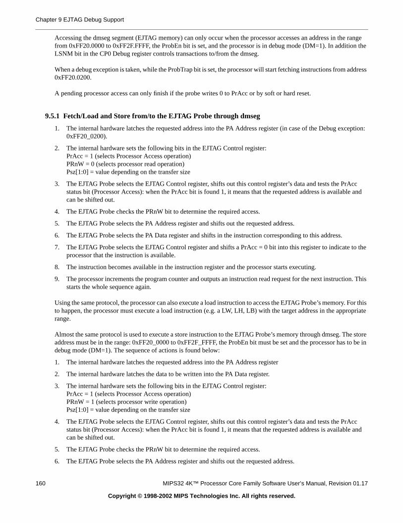
Chapter 9 EJTAG Debug Support
he rangeon the
ddress
xception:
rAccble and
to the
on. This
. For thisropriate
e stores to be in
rAccble and
Accessing the dmseg segment (EJTAG memory) can only occur when the processor accesses an address in tfrom 0xFF20.0000 to 0xFF2F.FFFF, the ProbEn bit is set, and the processor is in debug mode (DM=1). In additiLSNM bit in the CP0 Debug register controls transactions to/from the dmseg.
When a debug exception is taken, while the ProbTrap bit is set, the processor will start fetching instructions from a0xFF20.0200.
A pending processor access can only finish if the probe writes 0 to PrAcc or by soft or hard reset.
9.5.1 Fetch/Load and Store from/to the EJTAG Probe through dmseg
1. The internal hardware latches the requested address into the PA Address register (in case of the Debug e0xFF20_0200).
2. The internal hardware sets the following bits in the EJTAG Control register:PrAcc = 1 (selects Processor Access operation)PRnW = 0 (selects processor read operation)Psz[1:0] = value depending on the transfer size
3. The EJTAG Probe selects the EJTAG Control register, shifts out this control register’s data and tests the Pstatus bit (Processor Access): when the PrAcc bit is found 1, it means that the requested address is availacan be shifted out.
4. The EJTAG Probe checks the PRnW bit to determine the required access.
5. The EJTAG Probe selects the PA Address register and shifts out the requested address.
6. The EJTAG Probe selects the PA Data register and shifts in the instruction corresponding to this address.
7. The EJTAG Probe selects the EJTAG Control register and shifts a PrAcc = 0 bit into this register to indicateprocessor that the instruction is available.
8. The instruction becomes available in the instruction register and the processor starts executing.
9. The processor increments the program counter and outputs an instruction read request for the next instructistarts the whole sequence again.
Using the same protocol, the processor can also execute a load instruction to access the EJTAG Probe’s memoryto happen, the processor must execute a load instruction (e.g. a LW, LH, LB) with the target address in the apprange.
Almost the same protocol is used to execute a store instruction to the EJTAG Probe’s memory through dmseg. Thaddress must be in the range: 0xFF20_0000 to 0xFF2F_FFFF, the ProbEn bit must be set and the processor hadebug mode (DM=1). The sequence of actions is found below:
1. The internal hardware latches the requested address into the PA Address register
2. The internal hardware latches the data to be written into the PA Data register.
3. The internal hardware sets the following bits in the EJTAG Control register:PrAcc = 1 (selects Processor Access operation)PRnW = 1 (selects processor write operation)Psz[1:0] = value depending on the transfer size
4. The EJTAG Probe selects the EJTAG Control register, shifts out this control register’s data and tests the Pstatus bit (Processor Access): when the PrAcc bit is found 1, it means that the requested address is availacan be shifted out.
5. The EJTAG Probe checks the PRnW bit to determine the required access.
6. The EJTAG Probe selects the PA Address register and shifts out the requested address.
160 MIPS32 4K™ Processor Core Family Software User’s Manual, Revision 01.17
Copyright © 1998-2002 MIPS Technologies Inc. All rights reserved.
9.5 Processor Accesses
to the
7. The EJTAG Probe selects the PA Data register and shifts out the data to be written.
8. The EJTAG Probe selects the EJTAG Control register and shifts a PrAcc = 0 bit into this register to indicateprocessor that the write access is finished.
9. The EJTAG Probe writes the data to the requested address in its memory.
10. The processor detects that PrAcc bit = 0, which means that it is ready to handle a new access.
The above examples imply that no reset occurs during the operations, and that Rocc is cleared.
MIPS32 4K™ Processor Core Family Software User’s Manual, Revision 01.17 161
Copyright © 1998-2002 MIPS Technologies Inc. All rights reserved.

Chapter 9 EJTAG Debug Support
162 MIPS32 4K™ Processor Core Family Software User’s Manual, Revision 01.17
Copyright © 1998-2002 MIPS Technologies Inc. All rights reserved.

ediate,
rmats
less
Chapter 10
Instruction Set Overview
This chapter provides a general overview on the three CPU instruction set formats of the MIPS architecture: ImmJump, and Register. Refer toChapter 11, “MIPS32 4K Processor Core Instructions,” on page 169for a complete listingand description of instructions.
This chapter discusses the following topics:
• Section 10.1, "CPU Instruction Formats"
• Section 10.2, "Load and Store Instructions"
• Section 10.3, "Computational Instructions"
• Section 10.4, "Jump and Branch Instructions"
• Section 10.5, "Control Instructions"
• Section 10.6, "Coprocessor Instructions"
• Section 10.7, "Enhancements to the MIPS Architecture"
10.1 CPU Instruction Formats
Each CPU instruction consists of a single 32-bit word, aligned on a word boundary. There are three instruction foimmediate (I-type), jump (J-type), and register (R-type)—as shown inFigure 10-1. The use of a small number ofinstruction formats simplifies instruction decoding, allowing the compiler to synthesize more complicated (and frequently used) operations and addressing modes from these three formats as needed.
MIPS32 4K™ Processor Core Family Software User’s Manual, Revision 01.17 163
Copyright © 1998-2002 MIPS Technologies Inc. All rights reserved.
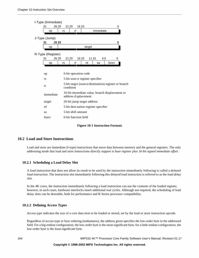
Chapter 10 Instruction Set Overview
he only
ster,of load
ode.
ddressedn, the
Figure 10-1 Instruction Formats
10.2 Load and Store Instructions
Load and store are immediate (I-type) instructions that move data between memory and the general registers. Taddressing mode that load and store instructions directly support isbase register plus 16-bit signed immediate offset.
10.2.1 Scheduling a Load Delay Slot
A load instruction that does not allow its result to be used by the instruction immediately following is called adelayedload instruction. The instruction slot immediately following this delayed load instruction is referred to as theload delayslot.
In the 4K cores, the instruction immediately following a load instruction can use the contents of the loaded regihowever, in such cases, hardware interlocks insert additional real cycles. Although not required, the schedulingdelay slots can be desirable, both for performance and R-Series processor compatibility.
10.2.2 Defining Access Types
Access type indicates the size of a core data item to be loaded or stored, set by the load or store instruction opc
Regardless of access type or byte ordering (endianness), the address given specifies the low-order byte in the afield. For a big-endian configuration, the low-order byte is the most-significant byte; for a little-endian configuratiolow-order byte is the least-significant byte.
op 6-bit operation code
rs 5-bit source register specifier
rt 5-bit target (source/destination) register or branchcondition
immediate 16-bit immediate value, branch displacement oraddress displacement
target 26-bit jump target address
rd 5-bit destination register specifier
sa 5-bit shift amount
funct 6-bit function field
I-Type (Immediate)
R-Type (Register)
J-Type (Jump)
immediate
015
rt
1620
op
2631
rs
2125
target
015
op
2631
rt
1620
op
2631
rs
2125
sa
610
rd
1115
funct
05
target
025
op
2631
164 MIPS32 4K™ Processor Core Family Software User’s Manual, Revision 01.17
Copyright © 1998-2002 MIPS Technologies Inc. All rights reserved.
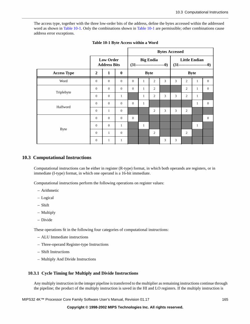
10.3 Computational Instructions
dressed
ough is
The access type, together with the three low-order bits of the address, define the bytes accessed within the adword as shown inTable 10-1. Only the combinations shown inTable 10-1 are permissible; other combinations causeaddress error exceptions.
10.3 Computational Instructions
Computational instructions can be either in register (R-type) format, in which both operands are registers, or inimmediate (I-type) format, in which one operand is a 16-bit immediate.
Computational instructions perform the following operations on register values:
– Arithmetic
– Logical
– Shift
– Multiply
– Divide
These operations fit in the following four categories of computational instructions:
– ALU Immediate instructions
– Three-operand Register-type Instructions
– Shift Instructions
– Multiply And Divide Instructions
10.3.1 Cycle Timing for Multiply and Divide Instructions
Any multiply instruction in the integer pipeline is transferred to the multiplier as remaining instructions continue thrthe pipeline; the product of the multiply instruction is saved in the HI and LO registers. If the multiply instruction
Table 10-1 Byte Access within a Word
Bytes Accessed
Low OrderAddress Bits
Big Endia(31---------------------0)
Little Endian(31---------------------0)
Access Type 2 1 0 Byte Byte
Word 0 0 0 0 1 2 3 3 2 1 0
Triplebyte0 0 0 0 1 2 2 1 0
0 0 1 1 2 3 3 2 1
Halfword0 0 0 0 1 1 0
0 1 0 2 3 3 2
Byte
0 0 0 0 0
0 0 1 1 1
0 1 0 2 2
0 1 1 3 3
MIPS32 4K™ Processor Core Family Software User’s Manual, Revision 01.17 165
Copyright © 1998-2002 MIPS Technologies Inc. All rights reserved.

Chapter 10 Instruction Set Overview
come
delayn in
th of
d Linkeral
to the
followed by an MFHI or MFLO before the product is available, the pipeline interlocks until this product does beavailable. Refer toChapter 2, “Pipeline,” for more information on instruction latency and repeat rates.
10.4 Jump and Branch Instructions
Jump and branch instructions change the control flow of a program. All jump and branch instructions occur with aof one instruction: that is, the instruction immediately following the jump or branch (this is known as the instructiothedelay slot) always executes while the target instruction is being fetched from storage.
10.4.1 Overview of Jump Instructions
Subroutine calls in high-level languages are usually implemented with Jump or Jump and Link instructions, bowhich are J-type instructions. In J-type format, the 26-bit target address shifts left 2 bits and combines with thehigh-order 4 bits of the current program counter to form an absolute address.
Returns, dispatches, and large cross-page jumps are usually implemented with the Jump Register or Jump anRegister instructions. Both are R-type instructions that take the 32-bit byte address contained in one of the genpurpose registers.
For more information about jump instructions, refer to the individual instructions inSection 11.3, "Instruction Set".
10.4.2 Overview of Branch Instructions
All branch instruction target addresses are computed by adding the address of the instruction in the delay slot 16-bitoffset (shifted left 2 bits and sign-extended to 32 bits). All branches occur with a delay of one instruction.
If a conditional branch likely is not taken, the instruction in the delay slot is nullified.
Branches, jumps, ERET, and DERET instructions should not be placed in the delay slot of a branch or jump.
10.5 Control Instructions
Control instructions allow the software to initiate traps; they are always R-type.
10.6 Coprocessor Instructions
CP0 instructions perform operations on the System Control Coprocessor registers to manipulate the memorymanagement and exception handling facilities of the processor. Refer to ChapterChapter 11, “MIPS32 4K ProcessorCore Instructions,” on page 169 for a listing of CP0 instructions.
10.7 Enhancements to the MIPS Architecture
The core execution unit implements the MIPS32 architecture, which includes the following instructions.
• CLO – Count Leading Ones
• CLZ – Count Leading Zeros
• MADD – Multiply and Add Word
166 MIPS32 4K™ Processor Core Family Software User’s Manual, Revision 01.17
Copyright © 1998-2002 MIPS Technologies Inc. All rights reserved.

10.7 Enhancements to the MIPS Architecture
PR
PR
theult.
written
ordce
g value
alue-bit
value
2-bit toair. Thetances.
• MADDU – Multiply and Add Unsigned Word
• MSUB – Multiply and Subtract Word
• MSUBU – Multiply and Subtract Unsigned Word
• MUL – Multiply Word to Register
• SSNOP – Superscalar Inhibit NOP
10.7.1 CLO - Count Leading Ones
The CLO instruction counts the number of leading ones in a word. The 32-bit word in the GPRrs is scanned frommost-significant to least-significant bit. The number of leading ones is counted and the result is written to the Grd.If all 32 bits are set in the GPRrs, the result written to the GPRrd is 32.
10.7.2 CLZ - Count Leading Zeros
The CLZ instruction counts the number of leading zeros in a word. The 32-bit word in the GPRrs is scanned frommost-significant to least-significant bit. The number of leading zeros is counted and the result is written to the Grd.If all 32 bits are cleared in the GPRrs, the result written to the GPRrd is 32.
10.7.3 MADD - Multiply and Add Word
The MADD instruction multiplies two words and adds the result to the HI/LO register pair. The 32-bit word value inGPRrs is multiplied by the 32-bit value in the GPRrt, treating both operands as signed values, to produce a 64-bit resThe product is added to the 64-bit concatenated values in the HI and LO register pair. The resulting value is thenback to the HI and LO registers. No arithmetic exception occurs under any circumstances.
10.7.4 MADDU - Multiply and Add Unsigned Word
The MADDU instruction multiplies two unsigned words and adds the result to the HI/LO register pair. The 32-bit wvalue in the GPRrs is multiplied by the 32-bit value in the GPRrt, treating both operands as unsigned values, to produa 64-bit result. The product is added to the 64-bit concatenated values in the HI and LO register pair. The resultinis then written back to the HI and LO registers. No arithmetic exception occurs under any conditions.
10.7.5 MSUB - Multiply and Subtract Word
The MSUB instruction multiplies two words and subtracts the result from the HI/LO register pair. The 32-bit word vin the GPRrs is multiplied by the 32-bit value in the GPRrt, treating both operands as signed values, to produce a 64result. The product is subtracted from the 64-bit concatenated values in the HI and LO register pair. The resultingis then written back to the HI and LO registers. No arithmetic exception occurs under any circumstances.
10.7.6 MSUBU - Multiply and Subtract Unsigned Word
The MSUBU instruction multiplies two unsigned words and subtracts the result from the HI/LO register pair. The 3word value in the GPRrs is multiplied by the 32-bit value in the GPRrt, treating both operands as unsigned values,produce a 64-bit result. The product is subtracted from the 64-bit concatenated values in the HI and LO register presulting value is then written back to the HI and LO registers. No arithmetic exception occurs under any circums
MIPS32 4K™ Processor Core Family Software User’s Manual, Revision 01.17 167
Copyright © 1998-2002 MIPS Technologies Inc. All rights reserved.
Chapter 10 Instruction Set Overview
he
10.7.7 MUL - Multiply Word
The MUL instruction multiplies two words and writes the result to a GPR. The 32-bit word value in the GPRrs ismultiplied by the 32-bit value in the GPRrt, treating both operands as signed values, to produce a 64-bit result. Tleast-significant 32 bits of the product are written to the GPRrd. The contents of the HI and LO register pair are notdefined after the operation. No arithmetic exception occurs under any circumstances.
10.7.8 SSNOP- Superscalar Inhibit NOP
The MIPS32 4K processor cores treats this instruction as a regular NOP.
168 MIPS32 4K™ Processor Core Family Software User’s Manual, Revision 01.17
Copyright © 1998-2002 MIPS Technologies Inc. All rights reserved.

hich is
ion
tion.
s
Chapter 11
MIPS32 4K Processor Core Instructions
This chapter provides a detailed guide to understanding the instruction set for the MIPS32 4K processor cores, wa subset of the MIPS32 architecture. The chapter is divided into the following sections:
• Section 11.1, "Understanding the Instruction Descriptions" on page 169
• Section 11.2, "CPU Opcode Map" on page 169
• Section 11.3, "Instruction Set" on page 171
11.1 Understanding the Instruction Descriptions
Refer to Volume II of the MIPS32 Architecture Reference Manual for more information about the instructiondescriptions. There is a description of the instruction fields, definition of terms, and a description function notatavailable in that document.
11.2 CPU Opcode Map
Key
• CAPITALIZED text indicates an opcode mnemonic
• Italicized text indicates to look at the specified opcode submap for further instruction bit decode
• Entries containing theα symbol indicate that a reserved instruction fault occurs if the core executes this instruc
• Entries containing theβ symbol indicate that a coprocessor unusable exception occurs if the core executes thiinstruction
Table 11-1 Encoding of theOpcode Field
opcode bits 28..26
0 1 2 3 4 5 6 7
bits 31..29 000 001 010 011 100 101 110 111
0 000 Special RegImm J JAL BEQ BNE BLEZ BGTZ
1 001 ADDI ADDIU SLTI SLTIU ANDI ORI XORI LUI
2 010 COP0 β β β BEQL BNEL BLEZL BGTZL
3 011 α α α α Special2 α α α4 100 LB LH LWL LW LBU LHU LWR α5 101 SB SH SWL SW α α SWR CACHE
6 110 LL β β PREF α β β α7 111 SC β β α α β β α
MIPS32 4K™ Processor Core Family Software User’s Manual, Revision 01.17 169
Copyright © 1998-2002 MIPS Technologies Inc. All rights reserved.
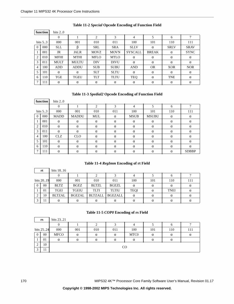
Chapter 11 MIPS32 4K Processor Core Instructions
Table 11-2Special Opcode Encoding of Function Field
function bits 2..0
0 1 2 3 4 5 6 7
bits 5..3 000 001 010 011 100 101 110 111
0 000 SLL β SRL SRA SLLV α SRLV SRAV
1 001 JR JALR MOVZ MOVN SYSCALL BREAK α SYNC
2 010 MFHI MTHI MFLO MTLO α α α α3 011 MULT MULTU DIV DIVU α α α α4 100 ADD ADDU SUB SUBU AND OR XOR NOR
5 101 α α SLT SLTU α α α α6 110 TGE TGEU TLT TLTU TEQ α TNE α7 111 α α α α α α α α
Table 11-3Spedial2 Opcode Encoding of Function Field
function bits 2..0
0 1 2 3 4 5 6 7
bits 5..3 000 001 010 011 100 101 110 111
0 000 MADD MADDU MUL α MSUB MSUBU α α1 001 α α α α α α α α2 010 α α α α α α α α3 011 α α α α α α α α4 100 CLZ CLO α α α α α α5 101 α α α α α α α α6 110 α α α α α α α α7 111 α α α α α α α SDBBP
Table 11-4RegImm Encoding of rt Field
rt bits 18..16
0 1 2 3 4 5 6 7
bits 20..19 000 001 010 011 100 101 110 111
0 00 BLTZ BGEZ BLTZL BGEZL α α α α1 01 TGEI TGEIU TLTI TLTIU TEQI α TNEI α2 10 BLTZAL BGEZAL BLTZALL BGEZALL α α α α3 11 α α α α α α α α
Table 11-5COP0 Encoding of rs Field
rs bits 23..21
0 1 2 3 4 5 6 7
bits 25..24 000 001 010 011 100 101 110 111
0 00 MFCO α α α MTC0 α α α1 01 α α α α α α α2 10
CO3 11
170 MIPS32 4K™ Processor Core Family Software User’s Manual, Revision 01.17
Copyright © 1998-2002 MIPS Technologies Inc. All rights reserved.

11.3 Instruction Set
d
11.3 Instruction Set
This section describes the core instructions.Table 11-7lists the instructions in alphabetical order, followed by a detailedescription of each instruction.
Table 11-6COP0 Encoding of Function Field When rs=CO
function bits 2..0
0 1 2 3 4 5 6 7
bits 5..3 000 001 010 011 100 101 110 111
0 000 α TLBR (4Kc)α (4Km/p)
TLBWI (4Kc)α (4Km/p) α α α TLBWR (4Kc)
α (4Km/p) α
1 001 TLBP (4Kc)α (4Km/p) α α α α α α α
2 010 α α α α α α α α3 011 ERET α α α α α α DERET
4 100 WAIT α α α α α α α5 101 α α α α α α α α6 110 α α α α α α α α7 111 α α α α α α α α
Table 11-7 Instruction Set
Instruction Description Function
ADD Integer Add Rd = Rs + Rt
ADDI Integer Add Immediate Rt = Rs + Immed
ADDIU Unsigned Integer Add Immediate Rt = Rs +U Immed
ADDU Unsigned Integer Add Rd = Rs +U Rt
AND Logical AND Rd = Rs & Rt
ANDI Logical AND Immediate Rt = Rs & (016 || Immed)
B Unconditional Branch(Asembler idiom for: BEQ r0, r0, offset) PC += (int)offset
BAL Branch and Link(Asembler idiom for: BGEZAL r0, offset)
GPR[31] = PC + 8PC += (int)offset
BEQ Branch On Equal if Rs == RtPC += (int)offset
BEQL Branch On Equal Likely
if Rs == RtPC += (int)offset
elseIgnore Next Instruction
BGEZ Branch on Greater Than or Equal To Zero if !Rs[31]PC += (int)offset
BGEZAL Branch on Greater Than or Equal To Zero AndLink
GPR[31] = PC + 8if !Rs[31]PC += (int)offset
MIPS32 4K™ Processor Core Family Software User’s Manual, Revision 01.17 171
Copyright © 1998-2002 MIPS Technologies Inc. All rights reserved.

Chapter 11 MIPS32 4K Processor Core Instructions
BGEZALL Branch on Greater Than or Equal To Zero AndLink Likely
GPR[31] = PC + 8if !Rs[31]PC += (int)offset
elseIgnore Next Instruction
BGEZL Branch on Greater Than or Equal To ZeroLikely
if !Rs[31]PC += (int)offset
elseIgnore Next Instruction
BGTZ Branch on Greater Than Zero if !Rs[31] && Rs != 0PC += (int)offset
BGTZL Branch on Greater Than Zero Likely
if !Rs[31] && Rs != 0PC += (int)offset
else Ignore Next Instruction
BLEZ Branch on Less Than or Equal to Zero if Rs[31] || Rs == 0PC += (int)offset
BLEZL Branch on Less Than or Equal to Zero Likely
if Rs[31] || Rs == 0PC += (int)offset
elseIgnore Next Instruction
BLTZ Branch on Less Than Zero if Rs[31]PC += (int)offset
BLTZAL Branch on Less Than Zero And LinkGPR[31] = PC + 8if Rs[31]PC += (int)offset
BLTZALL Branch on Less Than Zero And Link Likely
GPR[31] = PC + 8if Rs[31]PC += (int)offset
elseIgnore Next Instruction
BLTZL Branch on Less Than Zero Likely
if Rs[31]PC += (int)offset
elseIgnore Next Instruction
BNE Branch on Not Equal if Rs != RtPC += (int)offset
BNEL Branch on Not Equal Likely
if Rs != RtPC += (int)offset
elseIgnore Next Instruction
BREAK Breakpoint Break Exception
CACHE Cache Operation See Cache Description
COP0 Coprocessor 0 Operation See Coprocessor Description
CLO Count Leading Ones Rd = NumLeadingOnes(Rs)
CLZ Count Leading Zeroes Rd = NumLeadingZeroes(Rs)
DERET Return from Debug Exception PC = DEPCExit Debug Mode
Table 11-7 Instruction Set (Continued)
Instruction Description Function
172 MIPS32 4K™ Processor Core Family Software User’s Manual, Revision 01.17
Copyright © 1998-2002 MIPS Technologies Inc. All rights reserved.

11.3 Instruction Set
DIV Divide LO = (int)Rs / (int)RtHI = (int)Rs % (int)Rt
DIVU Unsigned Divide LO = (uns)Rs / (uns)RtHI = (uns)Rs % (uns)Rt
ERET Return from Exception
if SR[2]PC = ErrorEPC
elsePC = EPC
SR[1] = 0SR[2] = 0LL = 0
J Unconditional Jump PC = PC[31:28] || offset<<2
JAL Jump and Link GPR[31] = PC + 8PC = PC[31:28] || offset<<2
JALR Jump and Link Register Rd = PC + 8PC = Rs
JR Jump Register PC = Rs
LB Load Byte Rt = (byte)Mem[Rs+offset]
LBU Unsigned Load Byte Rt = (ubyte))Mem[Rs+offset]
LH Load Halfword Rt = (half)Mem[Rs+offset]
LHU Unsigned Load Halfword Rt = (uhalf)Mem[Rs+offset]
LL Load Linked WordRt = Mem[Rs+offset]LL = 1LLAdr = Rs + offset
LUI Load Upper Immediate Rt = immediate << 16
LW Load Word Rt = Mem[Rs+offset]
LWL Load Word Left Refer to Architecture ReferenceManual
LWR Load Word Right Refer to Architecture ReferenceManual
MADD Multiply-Add HI, LO += (int)Rs * (int)Rt
MADDU Multiply-Add Unsigned HI, LO += (uns)Rs * (uns)Rt
MFC0 Move From Coprocessor 0 Rt = CPR[0, n, sel] = Rt
MFHI Move From HI Rd = HI
MFLO Move From LO Rd = LO
MOVN Move Conditional on Not Zero if GPR[rt] ≠ 0 thenGPR[rd]← GPR[rs]
MOVZ Move Conditional on Zero if GPR[rt] = 0 thenGPR[rd]← GPR[rs]
MSUB Multiply-Subtract HI, LO -= (int)Rs * (int)Rt
MSUBU Multiply-Subtract Unsigned HI, LO -= (uns)Rs * (uns)Rt
Table 11-7 Instruction Set (Continued)
Instruction Description Function
MIPS32 4K™ Processor Core Family Software User’s Manual, Revision 01.17 173
Copyright © 1998-2002 MIPS Technologies Inc. All rights reserved.
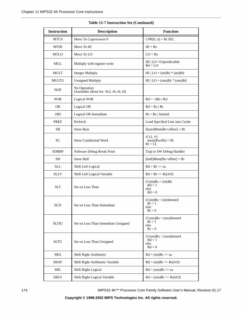
Chapter 11 MIPS32 4K Processor Core Instructions
MTC0 Move To Coprocessor 0 CPR[0, n] = Rt SEL
MTHI Move To HI HI = Rs
MTLO Move To LO LO = Rs
MUL Multiply with register write HI | LO =UnpredictableRd = LO
MULT Integer Multiply HI | LO = (int)Rs * (int)Rd
MULTU Unsigned Multiply HI | LO = (uns)Rs * (uns)Rd
NOP No Operation(Asembler idiom for: SLL r0, r0, r0)
NOR Logical NOR Rd = ~(Rs | Rt)
OR Logical OR Rd = Rs | Rt
ORI Logical OR Immediate Rt = Rs | Immed
PREF Prefetch Load Specified Line into Cache
SB Store Byte (byte)Mem[Rs+offset] = Rt
SC Store Conditional Wordif LL =1mem[Rxoffs] = Rt
Rt = LL
SDBBP Software Debug Break Point Trap to SW Debug Handler
SH Store Half (half)Mem[Rs+offset] = Rt
SLL Shift Left Logical Rd = Rt << sa
SLLV Shift Left Logical Variable Rd = Rt << Rs[4:0]
SLT Set on Less Than
if (int)Rs < (int)RtRd = 1
elseRd = 0
SLTI Set on Less Than Immediate
if (int)Rs < (int)ImmedRt = 1
elseRt = 0
SLTIU Set on Less Than Immediate Unsigned
if (uns)Rs < (uns)ImmedRt = 1
elseRt = 0
SLTU Set on Less Than Unsigned
if (uns)Rs < (uns)ImmedRd = 1
elseRd = 0
SRA Shift Right Arithmetic Rd = (int)Rt >> sa
SRAV Shift Right Arithmetic Variable Rd = (int)Rt >> Rs[4:0]
SRL Shift Right Logical Rd = (uns)Rt >> sa
SRLV Shift Right Logical Variable Rd = (uns)Rt >> Rs[4:0]
Table 11-7 Instruction Set (Continued)
Instruction Description Function
174 MIPS32 4K™ Processor Core Family Software User’s Manual, Revision 01.17
Copyright © 1998-2002 MIPS Technologies Inc. All rights reserved.

11.3 Instruction Set
SSNOP Superscalar Inhibit No Operation
SUB Integer Subtract Rt = (int)Rs - (int)Rd
SUBU Unsigned Subtract Rt = (uns)Rs - (uns)Rd
SW Store Word Mem[Rs+offset] = Rt
SWL Store Word Left Refer to Architecture ReferenceManual
SWR Store Word Right Refer to Architecture ReferenceManual
SYNC Synchronize See SYNC instruction onpage 194.
SYSCALL System Call SystemCallException
TEQ Trap if Equal if Rs == RtTrapException
TEQI Trap if Equal Immediate if Rs == (int)ImmedTrapException
TGE Trap if Greater Than or Equal if (int)Rs >= (int)RtTrapException
TGEI Trap if Greater Than or Equal Immediate if (int)Rs >= (int)ImmedTrapException
TGEIU Trap if Greater Than or Equal ImmediateUnsigned
if (uns)Rs >= (uns)ImmedTrapException
TGEU Trap if Greater Than or Equal Unsigned if (uns)Rs >= (uns)RtTrapException
TLBWI Write Indexed TLB Entry (4K core) See TLBWI instruction onpage 198.
TLBWR Write Random TLB Entry (4K core) See TLBWR instruction onpage 200.
TLBP Probe TLB for Matching Entry (4K core) See Architecture ReferenceManual.
TLBR Read Index for TLB Entry (4K core) See TLBR instruction onpage 196.
TLT Trap if Less Than if (int)Rs < (int)RtTrapException
TLTI Trap if Less Than Immediate if (int)Rs < (int)ImmedTrapException
TLTIU Trap if Less Than Immediate Unsigned if (uns)Rs < (uns)ImmedTrapException
TLTU Trap if Less Than Unsigned if (uns)Rs < (uns)RtTrapException
TNE Trap if Not Equal if Rs != RtTrapException
TNEI Trap if Not Equal Immediate if Rs != (int)ImmedTrapException
WAIT Wait for Interrupts Stall until interrupt occurs
Table 11-7 Instruction Set (Continued)
Instruction Description Function
MIPS32 4K™ Processor Core Family Software User’s Manual, Revision 01.17 175
Copyright © 1998-2002 MIPS Technologies Inc. All rights reserved.
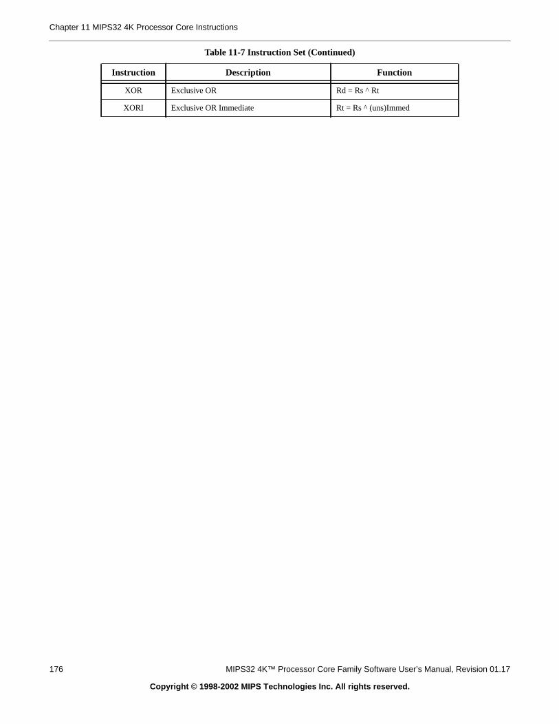
Chapter 11 MIPS32 4K Processor Core Instructions
XOR Exclusive OR Rd = Rs ^ Rt
XORI Exclusive OR Immediate Rt = Rs ^ (uns)Immed
Table 11-7 Instruction Set (Continued)
Instruction Description Function
176 MIPS32 4K™ Processor Core Family Software User’s Manual, Revision 01.17
Copyright © 1998-2002 MIPS Technologies Inc. All rights reserved.
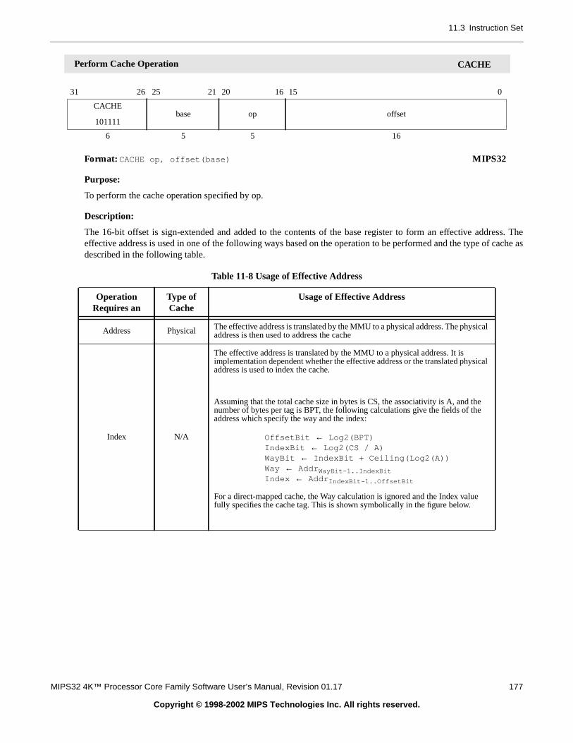
11.3 Instruction Set
ss. Theache as
CACHE
Format: CACHE op, offset(base) MIPS32
Purpose:
To perform the cache operation specified by op.
Description:
The 16-bit offset is sign-extended and added to the contents of the base register to form an effective addreeffective address is used in one of the following ways based on the operation to be performed and the type of cdescribed in the following table.
31 26 25 21 20 16 15 0
CACHE
101111base op offset
6 5 5 16
Table 11-8 Usage of Effective Address
OperationRequires an
Type ofCache
Usage of Effective Address
Address Physical The effective address is translated by the MMU to a physical address. The physicaladdress is then used to address the cache
Index N/A
The effective address is translated by the MMU to a physical address. It isimplementation dependent whether the effective address or the translated physicaladdress is used to index the cache.
Assuming that the total cache size in bytes is CS, the associativity is A, and thenumber of bytes per tag is BPT, the following calculations give the fields of theaddress which specify the way and the index:
OffsetBit ← Log2(BPT)IndexBit ← Log2(CS / A)WayBit ← IndexBit + Ceiling(Log2(A))Way ← Addr WayBit-1..IndexBitIndex ← Addr IndexBit-1..OffsetBit
For a direct-mapped cache, the Way calculation is ignored and the Index valuefully specifies the cache tag. This is shown symbolically in the figure below.
Perform Cache Operation CACHE
MIPS32 4K™ Processor Core Family Software User’s Manual, Revision 01.17 177
Copyright © 1998-2002 MIPS Technologies Inc. All rights reserved.

Chapter 11 MIPS32 4K Processor Core Instructions
dexould user TLB
ple, ifed via aion is
n of theinstruc-
tions,-based
Figure 11-1 Usage of Address Fields to Select Index and Way
A TLB Refill and TLB Invalid (both with cause code equal TLBL) exception can occur on any operation. For inoperations (where the address is used to index the cache but need not match the cache tag) software shunmapped addresses to avoid TLB exceptions. This instruction never causes TLB Modified exceptions noRefill exceptions with a cause code of TLBS, nor data Watch exceptions.
A Cache Error exception may occur as a byproduct of some operations performed by this instruction. For exama Writeback operation detects a cache or bus error during the processing of the operation, that error is reportCache Error exception. Similarly, a Bus Error Exception may occur if a bus operation invoked by this instructterminated in an error.
An address Error Exception (with cause code equal AdEL) occurs if the effective address references a portiokernel address space which would normally result in such an exception.Data watch is not triggered by a cachetion whose address matches the Watch register address match conditions.
Bits [17:16] of the instruction specify the cache on which to perform the operation, as follows:
Bits [20:18] of the instruction specify the operation to perform. .On Index Load Tag and Index Store Data operathe specific wordthat is addressed is loaded into / read from the DataLo . All other cache instructions are lineand the word and byte indexes will not affect their operation.
Table 11-9 Encoding of Bits[17:16] of CACHE Instruction
Code Name Cache
2#00 I Primary Instruction
2#01 D Primary Data
2#10 T Not supported
2#11 S Not supported
Perform Cache Operation CACHE
Way
0
Index
OffsetBitIndexBitWayBit
Unused byte index
178 MIPS32 4K™ Processor Core Family Software User’s Manual, Revision 01.17
Copyright © 1998-2002 MIPS Technologies Inc. All rights reserved.
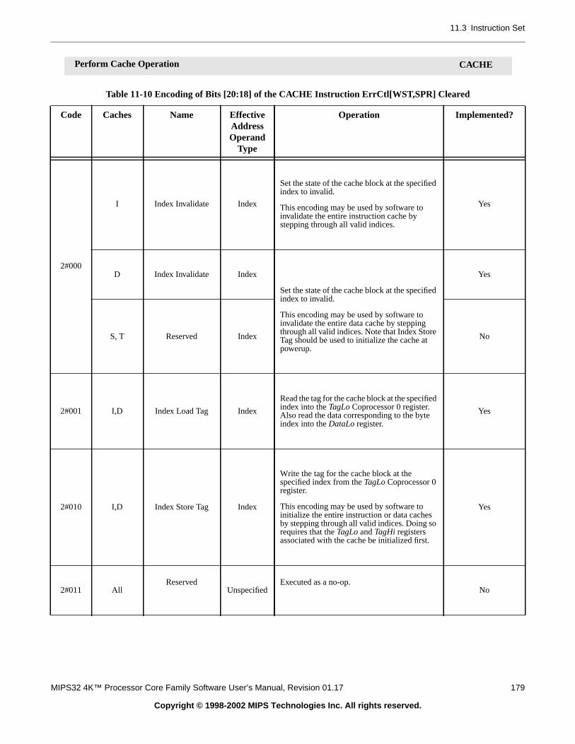
11.3 Instruction Set
Table 11-10 Encoding of Bits [20:18] of the CACHE Instruction ErrCtl[WST,SPR] Cleared
Code Caches Name EffectiveAddressOperand
Type
Operation Implemented?
2#000
I Index Invalidate Index
Set the state of the cache block at the specifiedindex to invalid.
This encoding may be used by software toinvalidate the entire instruction cache bystepping through all valid indices.
Yes
D Index Invalidate Index
Set the state of the cache block at the specifiedindex to invalid.
This encoding may be used by software toinvalidate the entire data cache by steppingthrough all valid indices. Note that Index StoreTag should be used to initialize the cache atpowerup.
Yes
S, T Reserved Index No
2#001 I,D Index Load Tag Index
Read the tag for the cache block at the specifiedindex into theTagLo Coprocessor 0 register.Also read the data corresponding to the byteindex into theDataLo register.
Yes
2#010 I,D Index Store Tag Index
Write the tag for the cache block at thespecified index from theTagLoCoprocessor 0register.
This encoding may be used by software toinitialize the entire instruction or data cachesby stepping through all valid indices. Doing sorequires that theTagLo andTagHi registersassociated with the cache be initialized first.
Yes
2#011 AllReserved
UnspecifiedExecuted as a no-op.
No
Perform Cache Operation CACHE
MIPS32 4K™ Processor Core Family Software User’s Manual, Revision 01.17 179
Copyright © 1998-2002 MIPS Technologies Inc. All rights reserved.

Chapter 11 MIPS32 4K Processor Core Instructions
2#100
I, D Hit Invalidate Address If the cache block contains the specifiedaddress, set the state of the cache block toinvalid.
This encoding may be used by software toinvalidate a range of addresses from theinstruction cache by stepping through theaddress range by the line size of the cache.
Yes
S, T Reserved Address No
2#101
I Fill Address
Fill the cache from the specified address.
The cache line is refetched even if it is alreadyin the cache. Yes
D Hit Invalidate Address If the cache block contains the specifiedaddress, set the state of the cache block toinvalid.
This encoding may be used by software toinvalidate a range of addresses from the datacache by stepping through the address range bythe line size of the cache.
Yes
S, T Reserved Address No
2#110
D Reserved Address
Executed as a no-op.
No
S, T Reserved Address No
2#111 I,D Fetch and Lock Address
If the cache does not contain the entire line atthe specified address, it is fetched frommemory, and the state is set to locked. If thecache already contains the line, set the state tolocked.
The lock state may be cleared by executing anIndex Invalidate or Hit Invalidate operation tothe locked line, or via an Index Store Tagoperation to the line that clears the lock bit.
Yes
Table 11-10 Encoding of Bits [20:18] of the CACHE Instruction ErrCtl[WST,SPR] Cleared
Code Caches Name EffectiveAddressOperand
Type
Operation Implemented?
180 MIPS32 4K™ Processor Core Family Software User’s Manual, Revision 01.17
Copyright © 1998-2002 MIPS Technologies Inc. All rights reserved.
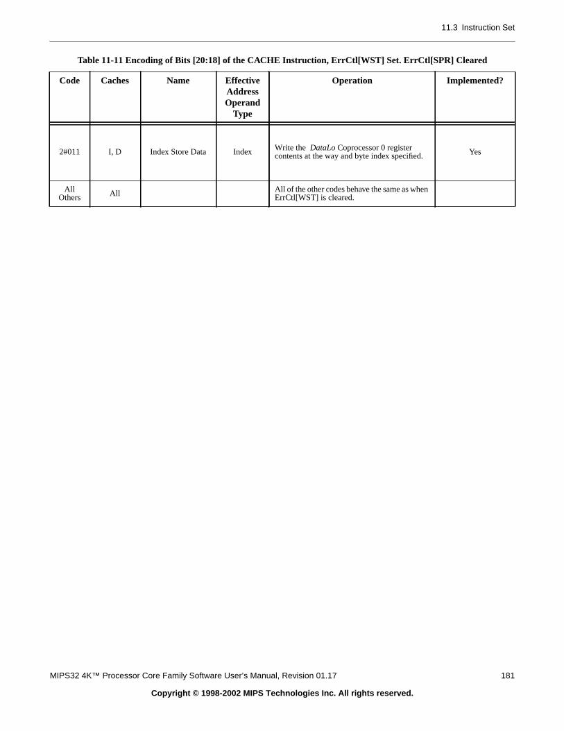
11.3 Instruction Set
Table 11-11 Encoding of Bits [20:18] of the CACHE Instruction, ErrCtl[WST] Set. ErrCtl[SPR] Cleared
Code Caches Name EffectiveAddressOperand
Type
Operation Implemented?
2#011 I, D Index Store Data Index Write the DataLo Coprocessor 0 registercontents at the way and byte index specified. Yes
AllOthers All All of the other codes behave the same as when
ErrCtl[WST] is cleared.
MIPS32 4K™ Processor Core Family Software User’s Manual, Revision 01.17 181
Copyright © 1998-2002 MIPS Technologies Inc. All rights reserved.

Chapter 11 MIPS32 4K Processor Core Instructions
Table 11-12 Encoding of Bits [20:18] of the CACHE Instruction, ErrCtl[SPR] Set
Code Caches Name EffectiveAddressOperand
Type
Operation Implemented?
2#001 I, D Index Load Tag Index Read the SPRAM tag at the specified index intotheTagLo Coprocessor 0 register. Yes
2#010 I, D Index Store Tag Index Update the SPRAM tag at the specified indexfrom theTagLo Coprocessor 0 register. Yes
2#011 I, D Index Store Data IndexWrite the DataLo Coprocessor 0 registercontents into the SPRAM at the word indexspecified.
Yes
AllOthers All All of the other codes behave the same as when
ErrCtl[SPR] is cleared.
182 MIPS32 4K™ Processor Core Family Software User’s Manual, Revision 01.17
Copyright © 1998-2002 MIPS Technologies Inc. All rights reserved.

11.3 Instruction Set
che-
Restrictions:
The operation of this instruction isUNDEFINED for any operation/cache combination that is not implemented.
The operation of this instruction isUNDEFINED if the operaation requires an address, and that address is uncaable.
Operation:
vAddr ← GPR[base] + sign_extend(offset)(pAddr, uncached) ← AddressTranslation(vAddr, DataReadReference)CacheOp(op, vAddr, pAddr)
Exceptions:
TLB Refill Exception.
TLB Invalid Exception
Coprocessor Unusable Exception
Address Error Exception
Bus Error Exception
Perform Cache Operation (cont.) CACHE
MIPS32 4K™ Processor Core Family Software User’s Manual, Revision 01.17 183
Copyright © 1998-2002 MIPS Technologies Inc. All rights reserved.

Chapter 11 MIPS32 4K Processor Core Instructions
s for
bitregister
ocessor.
e atomi-
fail on
MW
ress is
LL
Format: LL rt, offset(base) MIPS32
Purpose:
To load a word from memory for an atomic read-modify-write
Description: rt ← memory[base+offset]
The LL and SC instructions provide the primitives to implement atomic read-modify-write (RMW) operationcached memory locations.
The 16-bit signedoffsetis added to the contents of GPRbaseto form an effective address. The contents of the 32-word at the memory location specified by the aligned effective address are fetched, sign-extended to the GPRlength if necessary, and written into GPRrt.
This begins a RMW sequence on the current processor. There can be only one active RMW sequence per pr
When an LL is executed it starts an active RMW sequence replacing any other sequence that was active.
The RMW sequence is completed by a subsequent SC instruction that either completes the RMW sequenccally and succeeds, or does not and fails.
Executing LL on one processor does not cause an action that, by itself, causes an SC for the same block toanother processor.
An execution of LL does not have to be followed by execution of SC; a program is free to abandon the Rsequence without attempting a write.
Restrictions:
The addressed location must be cached; if it is not, the result is undefined.
The effective address must be naturally-aligned. If either of the 2 least-significant bits of the effective addnon-zero, an Address Error exception occurs.
Operation:
vAddr ← sign_extend(offset) + GPR[base]if vAddr 1..0 ≠ 0 2 then
SignalException(AddressError)endif(pAddr, CCA) ← AddressTranslation (vAddr, DATA, LOAD)memword ← LoadMemory (CCA, WORD, pAddr, vAddr, DATA)GPR[rt] ← memwordLLbit ← 1
31 26 25 21 20 16 15 0
LL
110000base rt offset
6 5 5 16
Load Linked Word LL
184 MIPS32 4K™ Processor Core Family Software User’s Manual, Revision 01.17
Copyright © 1998-2002 MIPS Technologies Inc. All rights reserved.

11.3 Instruction Set
Exceptions:
TLB Refill, TLB Invalid, Address Error, Reserved Instruction
Programming Notes:
There is no Load Linked Word Unsigned operation corresponding to Load Word Unsigned.
Load Linked Word (cont.) LL
MIPS32 4K™ Processor Core Family Software User’s Manual, Revision 01.17 185
Copyright © 1998-2002 MIPS Technologies Inc. All rights reserved.
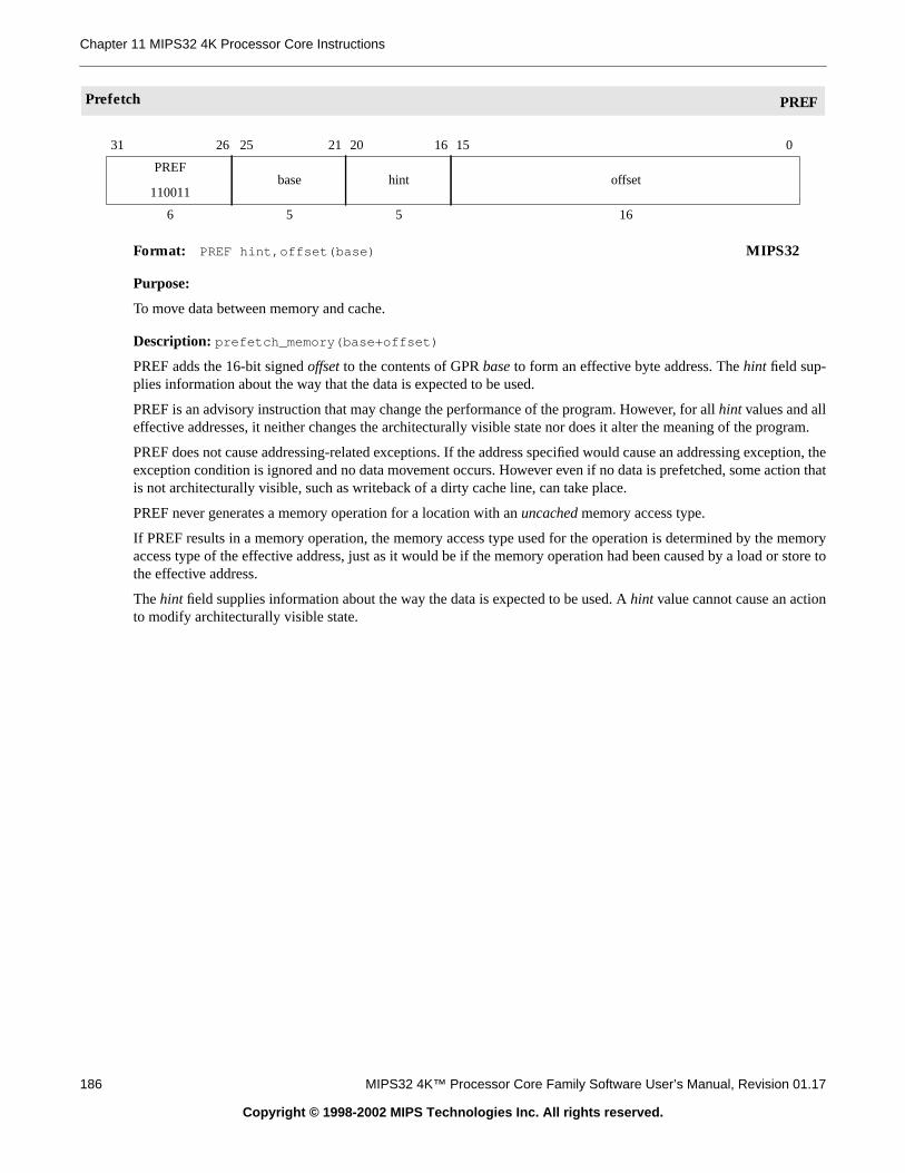
Chapter 11 MIPS32 4K Processor Core Instructions
gram.
eption, thetion that
emorystore to
PREF
Format: PREF hint,offset(base) MIPS32
Purpose:
To move data between memory and cache.
Description: prefetch_memory(base+offset)
PREF adds the 16-bit signedoffsetto the contents of GPRbaseto form an effective byte address. Thehint field sup-plies information about the way that the data is expected to be used.
PREF is an advisory instruction that may change the performance of the program. However, for allhint values and alleffective addresses, it neither changes the architecturally visible state nor does it alter the meaning of the pro
PREF does not cause addressing-related exceptions. If the address specified would cause an addressing excexception condition is ignored and no data movement occurs. However even if no data is prefetched, some acis not architecturally visible, such as writeback of a dirty cache line, can take place.
PREF never generates a memory operation for a location with anuncached memory access type.
If PREF results in a memory operation, the memory access type used for the operation is determined by the maccess type of the effective address, just as it would be if the memory operation had been caused by a load orthe effective address.
Thehint field supplies information about the way the data is expected to be used. Ahint value cannot cause an actionto modify architecturally visible state.
31 26 25 21 20 16 15 0
PREF
110011base hint offset
6 5 5 16
Prefetch PREF
186 MIPS32 4K™ Processor Core Family Software User’s Manual, Revision 01.17
Copyright © 1998-2002 MIPS Technologies Inc. All rights reserved.
11.3 Instruction Set
ans-to be
Any of the following conditions causes the 4K core to treat a PREF instruction as a NOP.
• A reservedhint value is used
• Writeback-invalidate (25)hint value is used
• The address has a translation error
• The address maps to an uncacheable page
• The data is already in the cache
• There is already another load/prefetch outstanding
In all other cases, except whenhint equals 25, execution of the PREF instruction initiates an external bus read traction. PREF is a non-blocking operation and does not cause the pipeline to stall while waiting for the datareturned.
Prefetch (cont.) PREF
MIPS32 4K™ Processor Core Family Software User’s Manual, Revision 01.17 187
Copyright © 1998-2002 MIPS Technologies Inc. All rights reserved.

Chapter 11 MIPS32 4K Processor Core Instructions
Table 11-13 Values of thehint Field for the PREF Instruction
Value Name Data Use and Desired Prefetch Action
0 loadUse: Prefetched data is expected to be read (not modified).
Action: Fetch data as if for a load.
1 storeUse: Prefetched data is expected to be stored or modified.
Action: Fetch data as if for a store.
2-3 Reserved Reserved - treated as a NOP.
4 load_streamed
Use: Prefetched data is expected to be read (not modified) but notreused extensively; it “streams” through cache.
Action: Fetch data as if for a load and place it in the cache so that itdoes not displace data prefetched as “retained.”
5 store_streamed
Use: Prefetched data is expected to be stored or modified but notreused extensively; it “streams” through cache.
Action: Fetch data as if for a store and place it in the cache so thatit does not displace data prefetched as “retained.”
6 load_retained
Use: Prefetched data is expected to be read (not modified) andreused extensively; it should be “retained” in the cache.
Action: Fetch data as if for a load and place it in the cache so that itis not displaced by data prefetched as “streamed.”
7 store_retained
Use: Prefetched data is expected to be stored or modified and reusedextensively; it should be “retained” in the cache.
Action: Fetch data as if for a store and place it in the cache so thatit is not displaced by data prefetched as “streamed.”
Prefetch (cont.) PREF
188 MIPS32 4K™ Processor Core Family Software User’s Manual, Revision 01.17
Copyright © 1998-2002 MIPS Technologies Inc. All rights reserved.
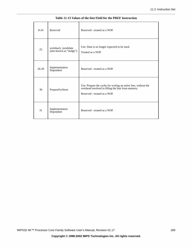
11.3 Instruction Set
8-24 Reserved Reserved - treated as a NOP.
25 writeback_invalidate(also known as “nudge”)
Use: Data is no longer expected to be used.
Treated as a NOP.
26-29ImplementationDependent Reserved - treated as a NOP.
30 PrepareForStore
Use: Prepare the cache for writing an entire line, without theoverhead involved in filling the line from memory.
Reserved - treated as a NOP.
31ImplementationDependent Reserved - treated as a NOP.
Table 11-13 Values of thehint Field for the PREF Instruction
MIPS32 4K™ Processor Core Family Software User’s Manual, Revision 01.17 189
Copyright © 1998-2002 MIPS Technologies Inc. All rights reserved.

Chapter 11 MIPS32 4K Processor Core Instructions
e TLB.prefetch
ss pointer
Restrictions:
None
Operation:
vAddr ← GPR[base] + sign_extend(offset)(pAddr, CCA) ← AddressTranslation(vAddr, DATA, LOAD)Prefetch(CCA, pAddr, vAddr, DATA, hint)
Exceptions:
Prefetch does not take any TLB-related or address-related exceptions under any circumstances.
Programming Notes:
Prefetch cannot prefetch data from a mapped location unless the translation for that location is present in thLocations in memory pages that have not been accessed recently may not have translations in the TLB, somay not be effective for such locations.
Prefetch does not cause addressing exceptions. It does not cause an exception to prefetch using an addrevalue before the validity of a pointer is determined.
Prefetch (cont.) PREF
190 MIPS32 4K™ Processor Core Family Software User’s Manual, Revision 01.17
Copyright © 1998-2002 MIPS Technologies Inc. All rights reserved.
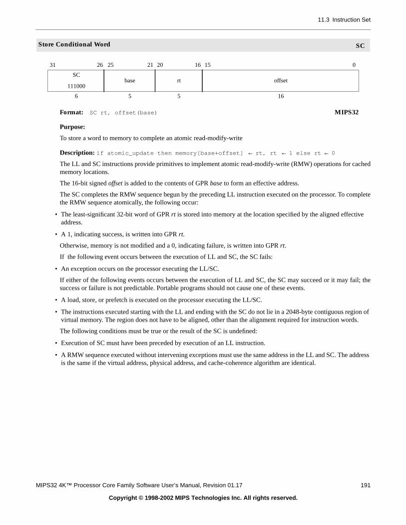
11.3 Instruction Set
ched
omplete
e
il; the
ion ofds.
address
SC
Format: SC rt, offset(base) MIPS32
Purpose:
To store a word to memory to complete an atomic read-modify-write
Description: if atomic_update then memory[base+offset] ← rt, rt ← 1 else rt ← 0
The LL and SC instructions provide primitives to implement atomic read-modify-write (RMW) operations for camemory locations.
The 16-bit signedoffset is added to the contents of GPRbaseto form an effective address.
The SC completes the RMW sequence begun by the preceding LL instruction executed on the processor. To cthe RMW sequence atomically, the following occur:
• The least-significant 32-bit word of GPRrt is stored into memory at the location specified by the aligned effectivaddress.
• A 1, indicating success, is written into GPRrt.
Otherwise, memory is not modified and a 0, indicating failure, is written into GPRrt.
If the following event occurs between the execution of LL and SC, the SC fails:
• An exception occurs on the processor executing the LL/SC.
If either of the following events occurs between the execution of LL and SC, the SC may succeed or it may fasuccess or failure is not predictable. Portable programs should not cause one of these events.
• A load, store, or prefetch is executed on the processor executing the LL/SC.
• The instructions executed starting with the LL and ending with the SC do not lie in a 2048-byte contiguous regvirtual memory. The region does not have to be aligned, other than the alignment required for instruction wor
The following conditions must be true or the result of the SC is undefined:
• Execution of SC must have been preceded by execution of an LL instruction.
• A RMW sequence executed without intervening exceptions must use the same address in the LL and SC. Theis the same if the virtual address, physical address, and cache-coherence algorithm are identical.
31 26 25 21 20 16 15 0
SC
111000base rt offset
6 5 5 16
Store Conditional Word SC
MIPS32 4K™ Processor Core Family Software User’s Manual, Revision 01.17 191
Copyright © 1998-2002 MIPS Technologies Inc. All rights reserved.
Chapter 11 MIPS32 4K Processor Core Instructions
rates
with
ader
with amic
ero, an
Atomic RMW is provided only for cached memory locations. The extent to which the detection of atomicity opecorrectly depends on the system implementation and the memory access type used for the location:
• MP atomicity: To provide atomic RMW among multiple processors, all accesses to the location must be madea memory access type ofcached coherent.
• Uniprocessor atomicity: To provide atomic RMW on a single processor, all accesses to the location must be mwith memory access type of eithercached noncoherent or cached coherent. All accesses must be to one or the otheaccess type, and they may not be mixed.
I/O System: To provide atomic RMW with a coherent I/O system, all accesses to the location must be madememory access type ofcached coherent. If the I/O system does not use coherent memory operations, then atoRMW cannot be provided with respect to the I/O reads and writes.
Restrictions:
The addressed location must have a memory access type ofcached noncoherentor cached coherent; if it does not, theresult is undefined.
The effective address must be naturally-aligned. If either of the 2 least-significant bits of the address is non-zAddress Error exception occurs.
Operation:
vAddr ← sign_extend(offset) + GPR[base]if vAddr 1..0 ≠ 0 2 then
SignalException(AddressError)endif(pAddr, CCA) ← AddressTranslation (vAddr, DATA, STORE)dataword ← GPR[rt]if LLbit then
StoreMemory (CCA, WORD, dataword, pAddr, vAddr, DATA)endifGPR[rt] ← 0 31 || LLbit
Store Conditional Word (cont.) SC
192 MIPS32 4K™ Processor Core Family Software User’s Manual, Revision 01.17
Copyright © 1998-2002 MIPS Technologies Inc. All rights reserved.
11.3 Instruction Set
mples ofre emu-
n
Exceptions:
TLB Refill, TLB Invalid, TLB Modified, Address Error, Reserved Instruction
Programming Notes:
LL and SC are used to atomically update memory locations, as shown below.
L1:LL T1, (T0) # load counterADDI T2, T1, 1 # incrementSC T2, (T0) # try to store, checking for atomicityBEQ T2, 0, L1 # if not atomic (0), try againNOP # branch-delay slot
Exceptions between the LL and SC cause SC to fail, so persistent exceptions must be avoided. Some exathese are arithmetic operations that trap, system calls, and floating point operations that trap or require softwalation assistance.
LL and SC function on a single processor forcached noncoherentmemory so that parallel programs can be run ouniprocessor systems that do not supportcached coherent memory access types.
Store Conditional Word (cont.) SC
MIPS32 4K™ Processor Core Family Software User’s Manual, Revision 01.17 193
Copyright © 1998-2002 MIPS Technologies Inc. All rights reserved.

Chapter 11 MIPS32 4K Processor Core Instructions
NC
isible to
iblexit from
ntil all
ore2
SYNC
Format: SYNC (stype = 0 implied) MIPS32
Purpose:
To order loads and stores.
Description:
Simple Description:
• SYNC affects onlyuncachedandcached coherentloads and stores. The loads and stores that occur before the SYmust be completed before the loads and stores after the SYNC are allowed to start.
• Loads are completed when the destination register is written. Stores are completed when the stored value is vevery other processor in the system.
• SYNC is required, potentially in conjunction with SSNOP, to guarantee that memory reference results are visacross operating mode changes. For example, a SYNC is required on some implementations on entry to and eDebug Mode to guarantee that memory affects are handled correctly.
Detailed Description:
• SYNC does not guarantee the order in which instruction fetches are performed. Thestype values 1-31 are reserved;they produce the same result as the value zero.
• Executing the SYNC instruction causes the write-through buffer to be flushed. The SYNC instruction stalls uloads and stores are completed.
• The innformation presented here refers to the MIPS 4K core implementation of the SYNC instruction. For a mdetailed description of the programming effects of SYNC on a generic MIPS32 processor, refer to the MIPS3Architecture Reference Manual.
31 26 25 21 20 16 15 11 10 6 5 0
SPECIAL
000000
0
00 0000 0000 0000 0stype
SYNC
001111
6 15 5 6
Synchronize Shared Memory SYNC
194 MIPS32 4K™ Processor Core Family Software User’s Manual, Revision 01.17
Copyright © 1998-2002 MIPS Technologies Inc. All rights reserved.

11.3 Instruction Set
Restrictions:
The effect of SYNC on the global order of loads and stores for memory access types other thanuncachedandcachedcoherent is UNPREDICTABLE .
Operation:SyncOperation(stype)
Exceptions:
None
Synchronize Shared Memory (cont.) SYNC
MIPS32 4K™ Processor Core Family Software User’s Manual, Revision 01.17 195
Copyright © 1998-2002 MIPS Technologies Inc. All rights reserved.

Chapter 11 MIPS32 4K Processor Core Instructions
to
ed
TLB
TLBR
Format: TLBR MIPS32
Purpose:
To read an entry from the TLB.
Description:
TheEntryHi, EntryLo0, EntryLo1, andPageMaskregisters are loaded with the contents of the TLB entry pointedby the Index register. Note that the value written to theEntryHi, EntryLo0, andEntryLo1registers may be differentfrom that originally written to the TLB via these registers in that:
• The value returned in the G bit in both theEntryLo0 andEntryLo1 registers comes from the single G bit in theTLB entry. Recall that this bit was set from the logical AND of the two G bits inEntryLo0 andEntryLo1 whenthe TLB was written.
• The value returned in the ASID field of theEntryHi register is zero for those chips that implement a BAT-basMMU organization.
Restrictions:
The operation isUNDEFINED if the contents of the Index register are greater than or equal to the number ofentries in the processor.
31 26 25 24 6 5 0
COP0
010000
CO
1
0
000 0000 0000 0000 0000
TLBR
000001
6 1 19 6
Read Indexed TLB Entry TLBR
196 MIPS32 4K™ Processor Core Family Software User’s Manual, Revision 01.17
Copyright © 1998-2002 MIPS Technologies Inc. All rights reserved.

11.3 Instruction Set
Operation:
i ← Indexif i > (TLBEntries - 1) then
UNDEFINEDendifPageMaskMask ← TLB[i] MaskEntryHi ←
TLB[i] VPN2 ||05 || TLB[i] ASID
EntryLo1 ← 0 2 ||TLB[i] PFN1 ||TLB[i] C1 || TLB[i] D1 || TLB[i] V1 || TLB[i] G
EntryLo0 ← 0 2 ||TLB[i] PFN0 ||TLB[i] C0 || TLB[i] D0 || TLB[i] V0 || TLB[i] G
Exceptions:
Coprocessor Unusable
Read Indexed TLB Entry TLBR
MIPS32 4K™ Processor Core Family Software User’s Manual, Revision 01.17 197
Copyright © 1998-2002 MIPS Technologies Inc. All rights reserved.
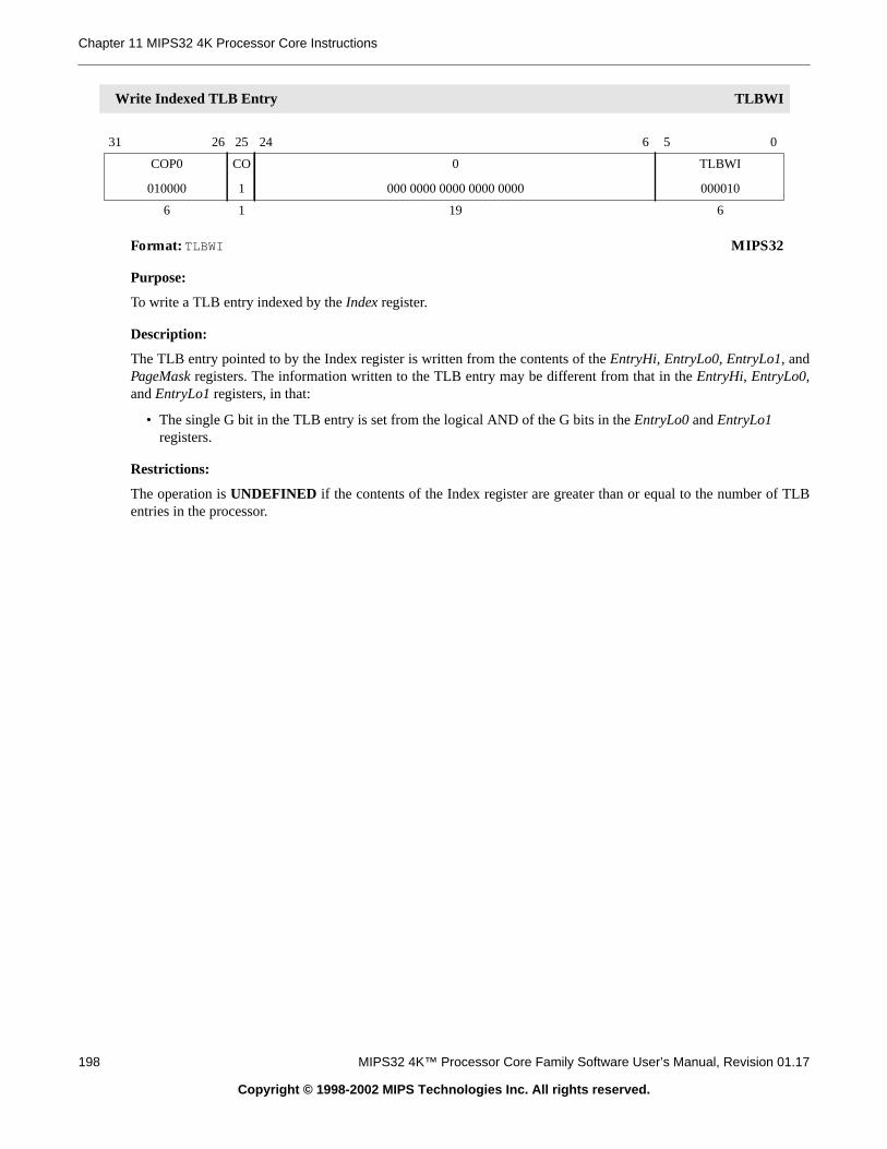
Chapter 11 MIPS32 4K Processor Core Instructions
TLB
TLBWI
Format: TLBWI MIPS32
Purpose:
To write a TLB entry indexed by theIndex register.
Description:
The TLB entry pointed to by the Index register is written from the contents of theEntryHi, EntryLo0, EntryLo1, andPageMaskregisters. The information written to the TLB entry may be different from that in theEntryHi, EntryLo0,andEntryLo1 registers, in that:
• The single G bit in the TLB entry is set from the logical AND of the G bits in theEntryLo0 andEntryLo1registers.
Restrictions:
The operation isUNDEFINED if the contents of the Index register are greater than or equal to the number ofentries in the processor.
31 26 25 24 6 5 0
COP0
010000
CO
1
0
000 0000 0000 0000 0000
TLBWI
000010
6 1 19 6
Write Indexed TLB Entry TLBWI
198 MIPS32 4K™ Processor Core Family Software User’s Manual, Revision 01.17
Copyright © 1998-2002 MIPS Technologies Inc. All rights reserved.

11.3 Instruction Set
Operation:
i ← IndexTLB[i] Mask ← PageMaskMaskTLB[i] VPN2 ← EntryHi VPN2TLB[i] ASID ← EntryHi ASIDTLB[i] G ← EntryLo1 G and EntryLo0 GTLB[i] PFN1 ← EntryLo1 PFNTLB[i] C1 ← EntryLo1 CTLB[i] D1 ← EntryLo1 DTLB[i] V1 ← EntryLo1 VTLB[i] PFN0 ← EntryLo0 PFNTLB[i] C0 ← EntryLo0 CTLB[i] D0 ← EntryLo0 DTLB[i] V0 ← EntryLo0 V
Exceptions:
Coprocessor Unusable
Write Indexed TLB Entry TLBWI
MIPS32 4K™ Processor Core Family Software User’s Manual, Revision 01.17 199
Copyright © 1998-2002 MIPS Technologies Inc. All rights reserved.

Chapter 11 MIPS32 4K Processor Core Instructions
TLB
TLBWR
Format: TLBWR MIPS32
Purpose:
To write a TLB entry indexed by theRandom register.
Description:
The TLB entry pointed to by theRandomregister is written from the contents of theEntryHi, EntryLo0, EntryLo1,and PageMaskregisters. The information written to the TLB entry may be different from that in theEntryHi,EntryLo0, andEntryLo1 registers, in that:
• The value returned in the G bit in both theEntryLo0 andEntryLo1 registers comes from the single G bit in theTLB entry. Recall that this bit was set from the logical AND of the two G bits inEntryLo0 andEntryLo1 whenthe TLB was written.
Restrictions:
The operation isUNDEFINED if the contents of the Index register are greater than or equal to the number ofentries in the processor.
31 26 25 24 6 5 0
COP0
010000
CO
1
0
000 0000 0000 0000 0000
TLBWR
000110
6 1 19 6
Write Random TLB Entry TLBWR
200 MIPS32 4K™ Processor Core Family Software User’s Manual, Revision 01.17
Copyright © 1998-2002 MIPS Technologies Inc. All rights reserved.

11.3 Instruction Set
Operation:
i ← RandomTLB[i] Mask ← PageMaskMaskTLB[i] VPN2 ← EntryHi VPN2TLB[i] ASID ← EntryHi ASIDTLB[i] G ← EntryLo1 G and EntryLo0 GTLB[i] PFN1 ← EntryLo1 PFNTLB[i] C1 ← EntryLo1 CTLB[i] D1 ← EntryLo1 DTLB[i] V1 ← EntryLo1 VTLB[i] PFN0 ← EntryLo0 PFNTLB[i] C0 ← EntryLo0 CTLB[i] D0 ← EntryLo0 DTLB[i] V0 ← EntryLo0 V
Exceptions:
Coprocessor Unusable
Write Random TLB Entry TLBWR
MIPS32 4K™ Processor Core Family Software User’s Manual, Revision 01.17 201
Copyright © 1998-2002 MIPS Technologies Inc. All rights reserved.

Chapter 11 MIPS32 4K Processor Core Instructions
sts areeset) iss do
a
WAIT
Format: WAIT MIPS32
Purpose:
Wait for Event
Description:
The WAIT instruction forces the core into low power mode. The pipeline is stalled and when all external requecompleted, the processor’s main clock is stopped. The processor will restart when reset (SI_Reset ro SI_ColdRsignaled, or a non-masked interrupt is taken (SI_NMI, SI_Int, or EJ_DINT). Note that the 4Kc, 4Kp & 4Km corenot use the code field in this instruction.
Restrictions:
The operation of the processor isUNDEFINED if a WAIT instruction is placed in the delay slot of a branch orjump.
31 26 25 24 6 5 0
COP0
010000
CO
1Implementation-Dependent Code
WAIT
100000
6 1 19 6
Enter Standby Mode WAIT
202 MIPS32 4K™ Processor Core Family Software User’s Manual, Revision 01.17
Copyright © 1998-2002 MIPS Technologies Inc. All rights reserved.

11.3 Instruction Set
Operation:
Enter lower power mode
Exceptions:
Coprocessor Unusable Exception
Enter Standby Mode (cont.) WAIT
MIPS32 4K™ Processor Core Family Software User’s Manual, Revision 01.17 203
Copyright © 1998-2002 MIPS Technologies Inc. All rights reserved.
Chapter 11 MIPS32 4K Processor Core Instructions
204 MIPS32 4K™ Processor Core Family Software User’s Manual, Revision 01.17
Copyright © 1998-2002 MIPS Technologies Inc. All rights reserved.

ante note of
change
ge barstion setin these
Appendix A
Revision History
In the left hand page margins of this document you may find vertical change bars to note the location of significchanges to this document since its last release. Significant changes are defined as those which you should takas you use the MIPS IP. Changes to correct grammar, spelling errors or similar may or may not be noted with bars. Change bars will be removed for changes which are more than one revision old.
Please note: Limitations on the authoring tools make it difficult to place change bars on changes to figures. Chanon figure titles are used to denote a potential change in the figure itself. Certain parts of this document (Instrucdescriptions, EJTAG register definitions) are references to Architecture specifications, and the change bars withsections indicate alterations since the previous version of the relevant Architecture document.
Revision Date Description
1.0 August, 1999 • First released version
MIPS32 4K™ Processor Core Family Software User’s Manual, Revision 01.17 205
Copyright © 1998-2002 MIPS Technologies Inc. All rights reserved.

Appendix A Revision History
1.1 November, 1999
• Re-organization to be more of a SoftWare User’s Manual.Removed System Interface chapter.
• Count register no longer stops incrementing in DebugMode -New bit added to Debug register to indicate this: CountDM
• New Bits added to Debug register for handling of impreciseexceptions: IEXI, DBusEP, IBusEP
• Added description of SubBlock ordering
• New MDU timing. Updated pipeline diagrams and text in Chap.2 to reflect new timing
• Modified Reset description. SoftReset cannot be masked by thecore. SoftReset does not need to be asserted when Reset isasserted
• ASID is not used in EJTAG breakpoint comparisons if the TLBis not implemented
• Added MT Compare to Timer Interrupt cleared to list of Hazardconditions
• Fixed Hazard from setting of SW Interrupt to Interruptedinstruction
• Changed SPECIAL opcode map to reflect MOVCI FP instn as aCoprocessor Instn rather than a Reserved Instn
• L2 Cache encodings of CACHE instn are reserved.
• Added note that I Fill CACHE instn will cause a re-fetch even ifthe line is in the cache
• MUL instn description reiterates that the contents of HI/LO areunpredictable after the MUL operation.
• Added ERL=1 as possible reason for being in kernel mode in thekseg descriptions
• Swapped priority of RI and CU exceptions
• Changed general exception code pseudo-code to have correctvector offset of 0x180
• Fixed typo in bus error description: stores OR non-criticalwords... not stores of non-critical words
• Changed TLBWI to TLBWR in Random register description
• Added note that behavior is undefined if illegal page mask valueis used
• Added note that StatusTS, StatusSR, and StatusNMI bits andCauseWP cannot be set by software
• Noted undefined behavior if StatusERL is set while executingcode in useg/kuseg
• Added Config1PC and Config1CA bits. Both wired to 0
Revision Date Description
206 MIPS32 4K™ Processor Core Family Software User’s Manual, Revision 01.17
Copyright © 1998-2002 MIPS Technologies Inc. All rights reserved.

1.1, continue November, 1999
• Changed Reset state of WatchI, WatchR, and WatchW to 0 fromundefined
• Removed some false statements about WAIT induced sleep mode
• CLO/CLZ instn description changed to reflect use of rd asdestination register instead of rt
• Add sel field to format statements in MFC0/MTC0 instns
• Removed redundant statement about writeback invalidate fromPREF instn
• Add programming note to multiply instructions that smallersource value should be placed in rt
• Updated listing of HW initialized Cop0 bits in Reset chapter
1.2 December, 1999 • Removed implication of internal mux for SI_TimerInt fromdescription of Compare register
01.03 January 28, 2000
• Cleaned up old references to ‘both’ cores
• Fixed some typos
• Fixed pipe stages in figure 2-12
• Added details on D-side micro TLB
• Cleaned up usage of trademarks
• Renamed title toMIPS32 4k™ Processor Core Family SoftwareUser’s Manual
• Changed revision numbering to xx.yy format for consistencywith other documents
01.04 March 23, 2000
• Cleaned up some old paragraph leftovers
• Changed look of Table of Contents, List of Figures and List ofTables
• Added timing information regarding Early In to divide algorithmfor 4Kc and 4Km
• Fixed CLO/CLZ description in section 10.7 to reflect rt -> rdchange in definition
• Cleaned up Config register definition. Defined BM field, definedreset state of several fields. Changed reserved fields to 0 fields
• Cleaned up decode tables - fixed font problems and multi-lineinstn text
• Updated PREF description
• Made reset state of StatusRP0
• Fixed some Spell-check issues.
01.05 May 8, 2000
• Clarified “Fetch and Lock” CACHE description.
• Removed text saying that the upper bits of PrID were availablefor implementors.
01.06 June 8, 2000• Rephrased field description of DataLo register.
• Updated copyright and trademark notices.
01.07 June 19, 2000 • Clarified initialization of Status.RP and WatchLo.{I,R,W} bitsduring Cold Reset in Chapters 4 and 5.
Revision Date Description
MIPS32 4K™ Processor Core Family Software User’s Manual, Revision 01.17 207
Copyright © 1998-2002 MIPS Technologies Inc. All rights reserved.
Appendix A Revision History
01.08 July 18, 2000
• Added bit numbering toTable 10-1 on page 165 describing theactive bytes in various access types
• Reformatted Cover sheet, added MD #
• Removed PrID column from this table
01.09 October 27, 2000
• Corrected PrRst bit in EJTAG Control Register to controlEJ_PrRst pin (was EJ_PerRst pin).
• Clarified use ofSI_Reset input in the Soft Reset description.
• Clarified effective address calculation in the description of theCACHE instruction.
• Small wording updates in the entire document.
• Added Scratch Pad bullet in Feature list.
• Added Multiply/divide bullet for 4Kp core in Feature list.
• Added Data-bypass section to Pipeline chapter.
• Added abbreviation explanation toFigure 2-1, Figure 2-2 andFigure 2-3.
• Corrected latency numbers for Divide inTable 2-1.
• ModifiedFigure 2-8, to make it more obvious what goes on.
• Corrected clock numbers for divide inFigure 2-11, Figure 2-12andFigure 2-13.
• Re-arrangedChapter 3, “Memory Management,” on page 31.Modes of operation is moved first, and JTLB entry contents isnow included in the TLB translation section.
• Changed SR to Status when CP0 Status register was referencedin Chapter 4, “Exceptions.”
• Changed some references from “instruction” to “data” in the databreakpoint section ofChapter 9, “EJTAG Debug Support.”
• Moved instruction Hazard section fromChapter 11, “MIPS32 4KProcessor Core Instructions,” to Chapter 2, “Pipeline.”
• Changed all references of Block Address Translation (BAT) toFixed Mapping (FM) for consistency with other MIPSdocuments.
01.10 October 31, 2000 • Converted document to new template.
01.11 December 4, 2000
• Fixed typo in opcodeTable 11-2 on page 170 (MUTLU ->MULTU).
• Changed MFCz/MTCz inTable 11-5 on page 170 toMFC0/MTC0.
01.12 January 3, 2001 • Made CountDM bit in Debug register read/write, so software cancontrol whether Count register increments in Debug Mode.
01.13 March 3, 2001• Miscellaneous minor text tweaks based on review feedback.
• Tagged source to make core specific document.
Revision Date Description
208 MIPS32 4K™ Processor Core Family Software User’s Manual, Revision 01.17
Copyright © 1998-2002 MIPS Technologies Inc. All rights reserved.

01.14 June 20, 2001
• Fixed some core specific tagging.
• Updated to document template revision 01.04
• Updated the instruction descriptions from the ArchitectureManual.
• Added missing footnote inTable 2-6 on page 28.
• Fixed typo in description of LSNM field inTable 5-26 on page102.
• Correct name of ASIDsup field in IBS (Table 9-7 on page 131)and DBS (Table 9-13 on page 137) registers.
• Correct name of ASIDuse field in IBCn (Table 9-11 on page 135)and DBCn (Table 9-17 on page 141) registers.
• Updated reset state of Doze and Halt bits in EJTAG Controlregister (Table 9-23 on page 153).
• First collom in sub-table for Psz field is changed from PA to PAA(Table 9-23 on page 153).
• Added a better Restriction example (subsequently removed inrevision 01.17).
• Added B, BAL and NOP to list of instructions (Table 11-7 onpage 171).
• In functions fields for LWL, LWR, SWL, SWR, SYNC, TLBWI,TLBWR, TLBP and TLBR. Pointed reader to see instructiondescription (Table 11-7 on page 171).
01.15 September 25, 2001• Added details on new core features - Index Store Data CACHEinstn, ErrCtl Cop0 register, EJTAG FASTDATA instruction
01.16 March 13, 2002
• Updated EJTAG Version in Debug register
• Added description of constant fields in Debug register - NoDCR,NoSSt, MCheckP, CacheEP, DDBSImpr, DDBLImpr
• Document SB bit in Config - indicates whether SimpleBE modeis active or not
• Added ISP,DSP bits in Config register. Indicate whetherISPRAM or DSPRAM are present.
01.17 September 25, 2002
• Remove instructions that are not implementation specific. Referto ISA documentation instead.
• Fixed 4Kp mul/div pipeline picture (Figure 2-3 on page 12)
Revision Date Description
MIPS32 4K™ Processor Core Family Software User’s Manual, Revision 01.17 209
Copyright © 1998-2002 MIPS Technologies Inc. All rights reserved.
Appendix A Revision History
210 MIPS32 4K™ Processor Core Family Software User’s Manual, Revision 01.17
Copyright © 1998-2002 MIPS Technologies Inc. All rights reserved.