mips32® 24k® processor core family software user’s manual
TRANSCRIPT

Document Number: MD00343Revision 03.11
December 19, 2008
MIPS Technologies, Inc. 955 East Arques Avenue
Sunnyvale, CA 94085-4521
Copyright © 2004-2008 MIPS Technologies Inc. All rights reserved.
MIPSVerified™
MIPS32® 24K® Processor Core FamilySoftware User’s Manual

MIPS32® 24K® Processor Core Family Software User’s Manual, Revision 03.11
Copyright © 2004-2008 MIPS Technologies Inc. All rights reserved.
Template: nB1.03, Built with tags: 2B MIPS32 PROC
Copyright © 2004-2008 MIPS Technologies, Inc. All rights reserved.
Unpublished rights (if any) reserved under the copyright laws of the United States of America and other countries.
This document contains information that is proprietary to MIPS Technologies, Inc. ("MIPS Technologies"). Any copying, reproducing, modifying or use ofthis information (in whole or in part) that is not expressly permitted in writing by MIPS Technologies or an authorized third party is strictly prohibited. At aminimum, this information is protected under unfair competition and copyright laws. Violations thereof may result in criminal penalties and fines.
Any document provided in source format (i.e., in a modifiable form such as in FrameMaker or Microsoft Word format) is subject to use and distributionrestrictions that are independent of and supplemental to any and all confidentiality restrictions. UNDER NO CIRCUMSTANCES MAY A DOCUMENTPROVIDED IN SOURCE FORMAT BE DISTRIBUTED TO A THIRD PARTY IN SOURCE FORMAT WITHOUT THE EXPRESS WRITTENPERMISSION OF MIPS TECHNOLOGIES, INC.
MIPS Technologies reserves the right to change the information contained in this document to improve function, design or otherwise. MIPS Technologies doesnot assume any liability arising out of the application or use of this information, or of any error or omission in such information. Any warranties, whetherexpress, statutory, implied or otherwise, including but not limited to the implied warranties of merchantability or fitness for a particular purpose, are excluded.Except as expressly provided in any written license agreement from MIPS Technologies or an authorized third party, the furnishing of this document does notgive recipient any license to any intellectual property rights, including any patent rights, that cover the information in this document.
The information contained in this document shall not be exported, reexported, transferred, or released, directly or indirectly, in violation of the law of anycountry or international law, regulation, treaty, Executive Order, statute, amendments or supplements thereto. Should a conflict arise regarding the export,reexport, transfer, or release of the information contained in this document, the laws of the United States of America shall be the governing law.
The information contained in this document constitutes one or more of the following: commercial computer software, commercial computer softwaredocumentation or other commercial items. If the user of this information, or any related documentation of any kind, including related technical data or manuals,is an agency, department, or other entity of the United States government ("Government"), the use, duplication, reproduction, release, modification, disclosure,or transfer of this information, or any related documentation of any kind, is restricted in accordance with Federal Acquisition Regulation 12.212 for civilianagencies and Defense Federal Acquisition Regulation Supplement 227.7202 for military agencies. The use of this information by the Government is furtherrestricted in accordance with the terms of the license agreement(s) and/or applicable contract terms and conditions covering this information from MIPSTechnologies or an authorized third party.
MIPS, MIPS I, MIPS II, MIPS III, MIPS IV, MIPS V, MIPS-3D, MIPS16, MIPS16e, MIPS32, MIPS64, MIPS-Based, MIPSsim, MIPSpro, MIPS Technologieslogo, MIPS-VERIFIED, MIPS-VERIFIED logo, 4K, 4Kc, 4Km, 4Kp, 4KE, 4KEc, 4KEm, 4KEp, 4KS, 4KSc, 4KSd, M4K, 5K, 5Kc, 5Kf, 24K, 24Kc, 24Kf,24KE, 24KEc, 24KEf, 34K, 34Kc, 34Kf, 74K, 74Kc, 74Kf, 1004K, 1004Kc, 1004Kf, R3000, R4000, R5000, ASMACRO, Atlas, "At the core of the userexperience.", BusBridge, Bus Navigator, CLAM, CorExtend, CoreFPGA, CoreLV, EC, FPGA View, FS2, FS2 FIRST SILICON SOLUTIONS logo, FS2NAVIGATOR, HyperDebug, HyperJTAG, JALGO, Logic Navigator, Malta, MDMX, MED, MGB, OCI, PDtrace, the Pipeline, Pro Series, SEAD, SEAD-2,SmartMIPS, SOC-it, System Navigator, and YAMON are trademarks or registered trademarks of MIPS Technologies, Inc. in the United States and othercountries.
All other trademarks referred to herein are the property of their respective owners.

MIPS32® 24K® Processor Core Family Software User’s Manual, Revision 03.11 3
Copyright © 2004-2008 MIPS Technologies Inc. All rights reserved.
Table of Contents
Chapter 1: Introduction to the MIPS32® 24K® Processor Core Family .......................................... 211.1: 24K® Core Features.................................................................................................................................. 221.2: 24K® Core Block Diagram ........................................................................................................................ 25
1.2.1: Logic Blocks ..................................................................................................................................... 261.2.1.1: Execution Unit ........................................................................................................................ 261.2.1.2: Multiply/Divide Unit (MDU) ..................................................................................................... 271.2.1.3: System Control Coprocessor (CP0) ....................................................................................... 271.2.1.4: Memory Management Unit (MMU) ......................................................................................... 271.2.1.5: Fetch Unit ............................................................................................................................... 281.2.1.6: Instruction Cache.................................................................................................................... 281.2.1.7: Load/Store Unit....................................................................................................................... 291.2.1.8: Data Cache............................................................................................................................. 291.2.1.9: Bus Interface Unit (BIU).......................................................................................................... 291.2.1.10: Power Management ............................................................................................................. 291.2.1.11: MIPS16e™ Application Specific Extension .......................................................................... 301.2.1.12: EJTAG Debug ...................................................................................................................... 301.2.1.13: CorExtend® User Defined Instructions................................................................................. 30
Chapter 2: Pipeline of the 24K® Core ................................................................................................. 312.1: Pipeline Stages.......................................................................................................................................... 31
2.1.1: IF Stage: Instruction Fetch First ....................................................................................................... 322.1.2: IS - Instruction Fetch Second........................................................................................................... 322.1.3: IR - Instruction Recode (MIPS16e only)........................................................................................... 332.1.4: IK - Instruction Kill (MIPS16e only) .................................................................................................. 332.1.5: IT - Instruction Fetch Third ............................................................................................................... 332.1.6: RF - Register File Access ................................................................................................................ 332.1.7: AG - Address Generation................................................................................................................. 332.1.8: EX - Execute/Memory Access.......................................................................................................... 332.1.9: MS - Memory Access Second.......................................................................................................... 332.1.10: ER- Exception Resolution .............................................................................................................. 342.1.11: WB - Writeback .............................................................................................................................. 34
2.2: Instruction Fetch ........................................................................................................................................ 342.2.1: Branch History Table........................................................................................................................ 37
2.2.1.1: Branch Target Calculation ...................................................................................................... 382.2.2: Return Prediction Stack ................................................................................................................... 382.2.3: ITLB.................................................................................................................................................. 382.2.4: Cache Miss Timing........................................................................................................................... 392.2.5: MIPS16e™....................................................................................................................................... 39
2.3: Load Store Unit.......................................................................................................................................... 402.3.1: DTLB................................................................................................................................................ 412.3.2: Data Cache Access.......................................................................................................................... 422.3.3: Outstanding misses.......................................................................................................................... 432.3.4: Uncached Accesses......................................................................................................................... 43
2.4: MDU Pipeline............................................................................................................................................. 432.4.1: Multiply Pipeline Stages ................................................................................................................... 452.4.2: Divide Operations............................................................................................................................. 47
2.5: Skewed ALU.............................................................................................................................................. 48

4 MIPS32® 24K® Processor Core Family Software User’s Manual, Revision 03.11
Copyright © 2004-2008 MIPS Technologies Inc. All rights reserved.
2.6: Interlock Handling...................................................................................................................................... 492.7: Instruction Interlocks.................................................................................................................................. 502.8: Hazards ..................................................................................................................................................... 51
2.8.1: Types of Hazards ............................................................................................................................. 512.8.1.1: Execution Hazards ................................................................................................................. 512.8.1.2: Instruction Hazards................................................................................................................. 52
2.8.2: Instruction Listing ............................................................................................................................. 532.8.2.1: Instruction Encoding ............................................................................................................... 53
2.8.3: Eliminating Hazards ......................................................................................................................... 54
Chapter 3: Floating-Point Unit of the 24Kf™ Core............................................................................. 553.1: Features Overview .................................................................................................................................... 55
3.1.1: IEEE Standard 754 .......................................................................................................................... 563.2: Enabling the Floating-Point Coprocessor .................................................................................................. 563.3: Data Formats............................................................................................................................................. 57
3.3.1: Floating-Point Formats..................................................................................................................... 573.3.1.1: Normalized and Denormalized Numbers................................................................................ 593.3.1.2: Reserved Operand Values—Infinity and NaN ........................................................................ 593.3.1.3: Infinity and Beyond ................................................................................................................. 593.3.1.4: Signalling Non-Number (SNaN) ............................................................................................. 593.3.1.5: Quiet Non-Number (QNaN) .................................................................................................... 59
3.3.2: Fixed-Point Formats......................................................................................................................... 603.4: Floating-Point General Registers .............................................................................................................. 61
3.4.1: FPRs and Formatted Operand Layout ............................................................................................. 613.4.2: Formats of Values Used in FP Registers ......................................................................................... 613.4.3: Binary Data Transfers (32-Bit and 64-Bit) ........................................................................................ 63
3.5: Floating-Point Control Registers................................................................................................................ 643.5.1: Floating-Point Implementation Register (FIR, CP1 Control Register 0)........................................... 653.5.2: Floating-Point Condition Codes Register (FCCR, CP1 Control Register 25)................................... 663.5.3: Floating-Point Exceptions Register (FEXR, CP1 Control Register 26) ............................................ 673.5.4: Floating-Point Enables Register (FENR, CP1 Control Register 28) ................................................ 673.5.5: Floating-Point Control and Status Register (FCSR, CP1 Control Register 31)................................ 683.5.6: Operation of the FS/FO/FN Bits ....................................................................................................... 70
3.5.6.1: Flush To Zero Bit .................................................................................................................... 713.5.6.2: Flush Override Bit ................................................................................................................... 723.5.6.3: Flush to Nearest ..................................................................................................................... 723.5.6.4: Recommended FS/FO/FN Settings........................................................................................ 73
3.5.7: FCSR Cause Bit Update Flow.......................................................................................................... 733.5.7.1: Exceptions Triggered by CTC1 .............................................................................................. 733.5.7.2: Generic Flow .......................................................................................................................... 733.5.7.3: Multiply-Add Flow ................................................................................................................... 743.5.7.4: Cause Update Flow for Input Operands ................................................................................. 743.5.7.5: Cause Update Flow for Unimplemented Operations .............................................................. 74
3.6: Instruction Overview .................................................................................................................................. 743.6.1: Data Transfer Instructions................................................................................................................ 75
3.6.1.1: Data Alignment in Loads, Stores, and Moves ........................................................................ 753.6.1.2: Addressing Used in Data Transfer Instructions ...................................................................... 75
3.6.2: Arithmetic Instructions...................................................................................................................... 763.6.3: Conversion Instructions.................................................................................................................... 773.6.4: Formatted Operand-Value Move Instructions .................................................................................. 783.6.5: Conditional Branch Instructions ....................................................................................................... 793.6.6: Miscellaneous Instructions ............................................................................................................... 79
3.7: Exceptions ................................................................................................................................................. 80

MIPS32® 24K® Processor Core Family Software User’s Manual, Revision 03.11 5
Copyright © 2004-2008 MIPS Technologies Inc. All rights reserved.
3.7.1: Precise Exception Mode .................................................................................................................. 803.7.2: Exception Conditions ....................................................................................................................... 80
3.7.2.1: Invalid Operation Exception.................................................................................................... 813.7.2.2: Division By Zero Exception..................................................................................................... 823.7.2.3: Underflow Exception............................................................................................................... 823.7.2.4: Overflow Exception................................................................................................................. 823.7.2.5: Inexact Exception ................................................................................................................... 823.7.2.6: Unimplemented Operation Exception..................................................................................... 83
3.8: Pipeline and Performance ......................................................................................................................... 833.8.1: Pipeline Overview ............................................................................................................................ 83
3.8.1.1: FR Stage - Decode, Register Read, and Unpack................................................................... 843.8.1.2: M1 Stage - Multiply Tree ........................................................................................................ 843.8.1.3: M2 Stage - Multiply Complete ................................................................................................ 843.8.1.4: A1 Stage - Addition First Step ................................................................................................ 843.8.1.5: A2 Stage - Addition Second and Final Step ........................................................................... 843.8.1.6: FP Stage - Result Pack .......................................................................................................... 843.8.1.7: FW Stage - Register Write...................................................................................................... 84
3.8.2: Bypassing......................................................................................................................................... 853.8.3: Repeat Rate and Latency ................................................................................................................ 85
Chapter 4: Memory Management of the 24K® Core .......................................................................... 874.1: Introduction................................................................................................................................................ 874.2: Modes of Operation ................................................................................................................................... 89
4.2.1: Virtual Memory Segments................................................................................................................ 894.2.1.1: Unmapped Segments............................................................................................................. 904.2.1.2: Mapped Segments ................................................................................................................. 91
4.2.2: User Mode........................................................................................................................................ 914.2.3: Supervisor Mode.............................................................................................................................. 924.2.4: Kernel Mode..................................................................................................................................... 94
4.2.4.1: Kernel Mode, User Space (kuseg) ......................................................................................... 964.2.4.2: Kernel Mode, Kernel Space 0 (kseg0).................................................................................... 964.2.4.3: Kernel Mode, Kernel Space 1 (kseg1).................................................................................... 964.2.4.4: Kernel Mode, Kernel/Supervisor Space 2 (ksseg/kseg2) ....................................................... 974.2.4.5: Kernel Mode, Kernel Space 3 (kseg3).................................................................................... 97
4.2.5: Debug Mode..................................................................................................................................... 974.2.5.1: Conditions and Behavior for Access to drseg, EJTAG Registers ........................................... 984.2.5.2: Conditions and Behavior for Access to dmseg, EJTAG Memory ........................................... 98
4.3: Translation Lookaside Buffer..................................................................................................................... 994.3.1: Joint TLB.......................................................................................................................................... 994.3.2: Instruction TLB............................................................................................................................... 1014.3.3: Data TLB........................................................................................................................................ 102
4.4: Virtual-to-Physical Address Translation................................................................................................... 1024.4.1: Hits, Misses, and Multiple Matches................................................................................................ 1044.4.2: Memory Space............................................................................................................................... 105
4.4.2.1: Page Sizes ........................................................................................................................... 1054.4.2.2: Replacement Algorithm ........................................................................................................ 105
4.4.3: TLB Instructions ............................................................................................................................. 1064.5: Fixed Mapping MMU ............................................................................................................................... 1074.6: System Control Coprocessor................................................................................................................... 109
Chapter 5: Exceptions and Interrupts in the 24K® Core................................................................. 1105.1: Exception Conditions............................................................................................................................... 1105.2: Exception Priority..................................................................................................................................... 111

6 MIPS32® 24K® Processor Core Family Software User’s Manual, Revision 03.11
Copyright © 2004-2008 MIPS Technologies Inc. All rights reserved.
5.3: Interrupts ................................................................................................................................................. 1125.3.1: Interrupt Modes .............................................................................................................................. 112
5.3.1.1: Interrupt Compatibility Mode................................................................................................. 1135.3.1.2: Vectored Interrupt Mode....................................................................................................... 1155.3.1.3: External Interrupt Controller Mode ....................................................................................... 118
5.3.2: Generation of Exception Vector Offsets for Vectored Interrupts .................................................... 1205.4: GPR Shadow Registers........................................................................................................................... 1215.5: Exception Vector Locations ..................................................................................................................... 1235.6: General Exception Processing ................................................................................................................ 1255.7: Debug Exception Processing .................................................................................................................. 1275.8: Exceptions ............................................................................................................................................... 129
5.8.1: Reset Exception ............................................................................................................................. 1295.8.2: Debug Single Step Exception ........................................................................................................ 1305.8.3: Debug Interrupt Exception ............................................................................................................. 1305.8.4: Non-Maskable Interrupt (NMI) Exception....................................................................................... 1315.8.5: Machine Check Exception.............................................................................................................. 1315.8.6: Interrupt Exception ......................................................................................................................... 1325.8.7: Debug Instruction Break Exception................................................................................................ 1325.8.8: Watch Exception — Instruction Fetch or Data Access................................................................... 1325.8.9: Address Error Exception — Instruction Fetch/Data Access........................................................... 1335.8.10: TLB Refill Exception — Instruction Fetch or Data Access ........................................................... 1345.8.11: TLB Invalid Exception — Instruction Fetch or Data Access......................................................... 1345.8.12: Cache Error Exception ................................................................................................................. 1355.8.13: Bus Error Exception — Instruction Fetch or Data Access............................................................ 1355.8.14: Debug Software Breakpoint Exception ........................................................................................ 1365.8.15: Execution Exception — System Call............................................................................................ 1365.8.16: Execution Exception — Breakpoint.............................................................................................. 1365.8.17: Execution Exception — Reserved Instruction .............................................................................. 1375.8.18: Execution Exception — Coprocessor Unusable .......................................................................... 1375.8.19: Execution Exception — CorExtend block Unusable .................................................................... 1385.8.20: Execution Exception — Floating Point Exception ........................................................................ 1385.8.21: Execution Exception — Integer Overflow..................................................................................... 1385.8.22: Execution Exception — Trap........................................................................................................ 1395.8.23: Execution Exception — C2E........................................................................................................ 1395.8.24: Execution Exception — IS1.......................................................................................................... 1395.8.25: Debug Data Break Exception....................................................................................................... 1395.8.26: TLB Modified Exception — Data Access ..................................................................................... 140
5.9: Exception Handling and Servicing Flowcharts ........................................................................................ 140
Chapter 6: CP0 Registers of the 24K® Core .................................................................................... 1466.1: CP0 Register Summary........................................................................................................................... 1466.2: CP0 Register Descriptions ...................................................................................................................... 148
6.2.1: Index Register (CP0 Register 0, Select 0) ..................................................................................... 1496.2.2: Random Register (CP0 Register 1, Select 0) ................................................................................ 1496.2.3: EntryLo0 and EntryLo1 Registers (CP0 Registers 2 and 3, Select 0)............................................ 1506.2.4: Context Register (CP0 Register 4, Select 0).................................................................................. 1516.2.5: UserLocal Register (CP0 Register 4, Select 2).............................................................................. 1526.2.6: PageMask Register (CP0 Register 5, Select 0) ............................................................................. 1536.2.7: Wired Register (CP0 Register 6, Select 0)..................................................................................... 1546.2.8: HWREna Register (CP0 Register 7, Select 0) ............................................................................... 1546.2.9: BadVAddr Register (CP0 Register 8, Select 0).............................................................................. 1566.2.10: Count Register (CP0 Register 9, Select 0) .................................................................................. 1576.2.11: EntryHi Register (CP0 Register 10, Select 0) .............................................................................. 157
MIPS32® 24K® Processor Core Family Software User’s Manual, Revision 03.11 7
Copyright © 2004-2008 MIPS Technologies Inc. All rights reserved.
6.2.12: Compare Register (CP0 Register 11, Select 0) ........................................................................... 1586.2.13: Status Register (CP0 Register 12, Select 0)................................................................................ 158
6.2.13.1: Operating Modes ................................................................................................................ 1596.2.13.2: Coprocessor Accessibility................................................................................................... 160
6.2.14: IntCtl Register (CP0 Register 12, Select 1).................................................................................. 1646.2.15: SRSCtl Register (CP0 Register 12, Select 2) .............................................................................. 1656.2.16: SRSMap Register (CP0 Register 12, Select 3)............................................................................ 1676.2.17: Cause Register (CP0 Register 13, Select 0)................................................................................ 1686.2.18: Exception Program Counter (CP0 Register 14, Select 0) ............................................................ 1726.2.19: Processor Identification (CP0 Register 15, Select 0) ................................................................... 1736.2.20: EBase Register (CP0 Register 15, Select 1) ............................................................................... 1736.2.21: Config Register (CP0 Register 16, Select 0)................................................................................ 1746.2.22: Config1 Register (CP0 Register 16, Select 1).............................................................................. 1766.2.23: Config2 Register (CP0 Register 16, Select 2).............................................................................. 1786.2.24: Config3 Register (CP0 Register 16, Select 3).............................................................................. 1806.2.25: Config7 Register (CP0 Register 16, Select 7).............................................................................. 1826.2.26: WatchLo Register (CP0 Register 18, Select 0-3)......................................................................... 1836.2.27: WatchHi Register (CP0 Register 19, Select 0-3) ......................................................................... 1846.2.28: Debug Register (CP0 Register 23, Select 0) ............................................................................... 1856.2.29: Trace Control Register (CP0 Register 23, Select 1) .................................................................... 1896.2.30: Trace Control2 Register (CP0 Register 23, Select 2) .................................................................. 1916.2.31: User Trace Data Register (CP0 Register 23, Select 3)................................................................ 1936.2.32: TraceIBPC Register (CP0 Register 23, Select 4) ........................................................................ 1936.2.33: TraceDBPC Register (CP0 Register 23, Select 5)....................................................................... 1946.2.34: Debug Exception Program Counter Register (CP0 Register 24, Select 0) .................................. 1956.2.35: Performance Counter Register (CP0 Register 25, select 0-3) ..................................................... 1966.2.36: ErrCtl Register (CP0 Register 26, Select 0)................................................................................. 2046.2.37: CacheErr Register (CP0 Register 27, Select 0)........................................................................... 2076.2.38: ITagLo Register (CP0 Register 28, Select 0)............................................................................... 2116.2.39: DTagLo Register (CP0 Register 28, Select 2 .............................................................................. 2126.2.40: L23TagLo Register (CP0 Register 28, Select 4).......................................................................... 2146.2.41: IDataLo Register (CP0 Register 28, Select 1) ............................................................................. 2146.2.42: DDataLo Register (CP0 Register 28, Select 3)............................................................................ 2146.2.43: L23DataLo Register (CP0 Register 28, Select 5) ........................................................................ 2156.2.44: IDataHi Register (CP0 Register 29, Select 1) .............................................................................. 2156.2.45: L23DataHi Register (CP0 Register 29, Select 5) ......................................................................... 2166.2.46: ErrorEPC (CP0 Register 30, Select 0) ......................................................................................... 2166.2.47: DeSave Register (CP0 Register 31, Select 0) ............................................................................. 217
Chapter 7: Hardware and Software Initialization of the 24K® Core ............................................... 2187.1: Hardware-Initialized Processor State ...................................................................................................... 218
7.1.1: Coprocessor 0 State ...................................................................................................................... 2187.1.2: TLB Initialization............................................................................................................................. 2197.1.3: Bus State Machines ....................................................................................................................... 2197.1.4: Static Configuration Inputs ............................................................................................................. 2197.1.5: Fetch Address ................................................................................................................................ 219
7.2: Software Initialized Processor State........................................................................................................ 2197.2.1: Register File ................................................................................................................................... 2207.2.2: TLB................................................................................................................................................. 2207.2.3: Caches ........................................................................................................................................... 2207.2.4: Coprocessor 0 State ...................................................................................................................... 220
Chapter 8: Caches of the 24K® Core ................................................................................................ 221

8 MIPS32® 24K® Processor Core Family Software User’s Manual, Revision 03.11
Copyright © 2004-2008 MIPS Technologies Inc. All rights reserved.
8.1: Cache Configurations .............................................................................................................................. 2218.2: Instruction Cache..................................................................................................................................... 221
8.2.1: Virtual Aliasing ............................................................................................................................... 2228.2.2: Precode Bits................................................................................................................................... 2238.2.3: Parity .............................................................................................................................................. 223
8.3: Data Cache.............................................................................................................................................. 2238.3.1: Virtual Aliasing ............................................................................................................................... 2248.3.2: Parity .............................................................................................................................................. 225
8.4: Write Back Buffer..................................................................................................................................... 2258.4.1: Uncached Accelerated Stores........................................................................................................ 226
8.5: Cache Protocols ...................................................................................................................................... 2278.5.1: Cache Organization ....................................................................................................................... 2278.5.2: Cacheability Attributes ................................................................................................................... 2278.5.3: Replacement Policy ....................................................................................................................... 2288.5.4: Line Locking ................................................................................................................................... 229
8.6: CACHE Instruction .................................................................................................................................. 2298.7: Software Cache Testing .......................................................................................................................... 230
8.7.1: I-Cache and D-cache Tag Arrays................................................................................................... 2308.7.2: I-Cache Data Array ........................................................................................................................ 2308.7.3: I-Cache WS Array .......................................................................................................................... 2308.7.4: D-Cache Data Array....................................................................................................................... 2308.7.5: D-cache WS Array ......................................................................................................................... 230
8.8: Memory Coherence Issues...................................................................................................................... 231
Chapter 9: Power Management in the 24K® Core ........................................................................... 2329.1: Register-Controlled Power Management ................................................................................................ 2329.2: Instruction-Controlled Power Management ............................................................................................. 233
9.2.1: Wait IE Ignore ................................................................................................................................ 233
Chapter 10: Instruction Set Overview............................................................................................... 23510.1: CPU Instruction Formats ....................................................................................................................... 23510.2: Load and Store Instructions................................................................................................................... 236
10.2.1: Scheduling a Load Delay Slot ...................................................................................................... 23610.2.2: Defining Access Types................................................................................................................. 236
10.3: Computational Instructions .................................................................................................................... 23710.3.1: Cycle Timing for Multiply and Divide Instructions......................................................................... 238
10.4: Jump and Branch Instructions ............................................................................................................... 23810.4.1: Overview of Jump Instructions ..................................................................................................... 23810.4.2: Overview of Branch Instructions .................................................................................................. 238
10.5: Control Instructions................................................................................................................................ 23910.6: Coprocessor Instructions....................................................................................................................... 239
Chapter 11: EJTAG Debug Support in the 24K® Core .................................................................... 24011.1: Debug Control Register ......................................................................................................................... 24111.2: Hardware Breakpoints ........................................................................................................................... 242
11.2.1: Features of Instruction Breakpoint ............................................................................................... 24311.2.2: Features of Data Breakpoint ........................................................................................................ 24311.2.3: Instruction Breakpoint Registers Overview .................................................................................. 24311.2.4: Data Breakpoint Registers Overview ........................................................................................... 24411.2.5: Conditions for Matching Breakpoints ........................................................................................... 244
11.2.5.1: Conditions for Matching Instruction Breakpoints ................................................................ 24411.2.5.2: Conditions for Matching Data Breakpoints ......................................................................... 245

MIPS32® 24K® Processor Core Family Software User’s Manual, Revision 03.11 9
Copyright © 2004-2008 MIPS Technologies Inc. All rights reserved.
11.2.6: Debug Exceptions from Breakpoints............................................................................................ 24611.2.6.1: Debug Exception by Instruction Breakpoint........................................................................ 24611.2.6.2: Debug Exception by Data Breakpoint................................................................................. 246
11.2.7: Breakpoint used as TriggerPoint.................................................................................................. 24811.2.8: Instruction Breakpoint Registers .................................................................................................. 248
11.2.8.1: Instruction Breakpoint Status (IBS) Register ...................................................................... 24811.2.8.2: Instruction Breakpoint Address n (IBAn) Register .............................................................. 24911.2.8.3: Instruction Breakpoint Address Mask n (IBMn) Register .................................................... 24911.2.8.4: Instruction Breakpoint ASID n (IBASIDn) Register ............................................................. 25011.2.8.5: Instruction Breakpoint Control n (IBCn) Register ............................................................... 250
11.2.9: Data Breakpoint Registers ........................................................................................................... 25111.2.9.1: Data Breakpoint Status (DBS) Register ............................................................................. 25111.2.9.2: Data Breakpoint Address n (DBAn) Register ..................................................................... 25211.2.9.3: Data Breakpoint Address Mask n (DBMn) Register ........................................................... 25211.2.9.4: Data Breakpoint ASID n (DBASIDn) Register .................................................................... 25311.2.9.5: Data Breakpoint Control n (DBCn) Register ....................................................................... 25311.2.9.6: Data Breakpoint Value n (DBVn) Register ......................................................................... 25411.2.9.7: Data Breakpoint Value High n (DBVHn) Register .............................................................. 255
11.3: Test Access Port (TAP) ......................................................................................................................... 25511.3.1: EJTAG Internal and External Interfaces....................................................................................... 25611.3.2: Test Access Port Operation ......................................................................................................... 256
11.3.2.1: Test-Logic-Reset State....................................................................................................... 25711.3.2.2: Run-Test/Idle State............................................................................................................. 25711.3.2.3: Select_DR_Scan State....................................................................................................... 25811.3.2.4: Select_IR_Scan State ........................................................................................................ 25811.3.2.5: Capture_DR State .............................................................................................................. 25811.3.2.6: Shift_DR State.................................................................................................................... 25811.3.2.7: Exit1_DR State ................................................................................................................... 25811.3.2.8: Pause_DR State................................................................................................................. 25811.3.2.9: Exit2_DR State ................................................................................................................... 25811.3.2.10: Update_DR State ............................................................................................................. 25911.3.2.11: Capture_IR State.............................................................................................................. 25911.3.2.12: Shift_IR State ................................................................................................................... 25911.3.2.13: Exit1_IR State................................................................................................................... 25911.3.2.14: Pause_IR State ................................................................................................................ 25911.3.2.15: Exit2_IR State................................................................................................................... 25911.3.2.16: Update_IR State ............................................................................................................... 259
11.3.3: Test Access Port (TAP) Instructions ............................................................................................ 26011.3.3.1: BYPASS Instruction............................................................................................................ 26011.3.3.2: IDCODE Instruction ............................................................................................................ 26011.3.3.3: IMPCODE Instruction ......................................................................................................... 26011.3.3.4: ADDRESS Instruction......................................................................................................... 26111.3.3.5: DATA Instruction ................................................................................................................ 26111.3.3.6: CONTROL Instruction ........................................................................................................ 26111.3.3.7: ALL Instruction.................................................................................................................... 26111.3.3.8: EJTAGBOOT Instruction .................................................................................................... 26111.3.3.9: NORMALBOOT Instruction ................................................................................................ 26111.3.3.10: FASTDATA Instruction ..................................................................................................... 26211.3.3.11: TCBCONTROLA Instruction............................................................................................. 26211.3.3.12: TCBCONTROLB Instruction............................................................................................. 26211.3.3.13: TCBCONTROLC Instruction............................................................................................. 26211.3.3.14: TCBDATA Instruction ....................................................................................................... 26211.3.3.15: PCSAMPLE Instruction .................................................................................................... 262

10 MIPS32® 24K® Processor Core Family Software User’s Manual, Revision 03.11
Copyright © 2004-2008 MIPS Technologies Inc. All rights reserved.
11.4: EJTAG TAP Registers........................................................................................................................... 26211.4.1: Instruction Register ...................................................................................................................... 26211.4.2: Data Registers Overview ............................................................................................................. 263
11.4.2.1: Bypass Register ................................................................................................................. 26311.4.2.2: Device Identification (ID) Register ...................................................................................... 26311.4.2.3: Implementation Register..................................................................................................... 26411.4.2.4: EJTAG Control Register ..................................................................................................... 265
11.4.3: Processor Access Address Register............................................................................................ 26911.4.3.1: Processor Access Data Register ........................................................................................ 269
11.4.4: Fastdata Register (TAP Instruction FASTDATA) ......................................................................... 27011.5: TAP Processor Accesses ...................................................................................................................... 271
11.5.1: Fetch/Load and Store From/To the EJTAG Probe Through dmseg............................................. 27111.6: PC Sampling.......................................................................................................................................... 273
11.6.1: PC Sampling in Wait State........................................................................................................... 27311.7: MIPS® Trace ......................................................................................................................................... 273
11.7.1: Processor Modes ......................................................................................................................... 27411.7.2: Software Versus Hardware Control.............................................................................................. 27411.7.3: Trace Information ......................................................................................................................... 27511.7.4: Load/Store Address and Data Trace Information......................................................................... 27611.7.5: Programmable Processor Trace Mode Options........................................................................... 27611.7.6: Programmable Trace Information Options ................................................................................... 276
11.7.6.1: User Data Trace ................................................................................................................. 27711.7.7: Enable Trace to Probe On-chip Memory...................................................................................... 27711.7.8: TCB Trigger.................................................................................................................................. 27711.7.9: Cycle-by-Cycle Information .......................................................................................................... 27711.7.10: Instruction and Data Cache Miss Tracing .................................................................................. 27711.7.11: Trace Message Format .............................................................................................................. 27811.7.12: Trace Word Format .................................................................................................................... 278
11.8: PDtrace™ Registers (Software Control)................................................................................................ 27811.9: Trace Control Block (TCB) Registers (Hardware Control)..................................................................... 279
11.9.1: TCBCONTROLA Register............................................................................................................ 27911.9.2: TCBCONTROLB Register............................................................................................................ 28211.9.3: TCBDATA Register ...................................................................................................................... 28511.9.4: TCBCONTROLC Register ........................................................................................................... 28611.9.5: TCBCONFIG Register (Reg 0)..................................................................................................... 28711.9.6: TCBTW Register (Reg 4) ............................................................................................................. 28811.9.7: TCBRDP Register (Reg 5) ........................................................................................................... 28811.9.8: TCBWRP Register (Reg 6) .......................................................................................................... 28911.9.9: TCBSTP Register (Reg 7)............................................................................................................ 28911.9.10: TCBTRIGx Register (Reg 16-23) ............................................................................................... 29011.9.11: Register Reset State .................................................................................................................. 292
11.10: Enabling MIPS Trace........................................................................................................................... 29311.10.1: Trace Trigger from EJTAG Hardware Instruction/Data Breakpoints .......................................... 29311.10.2: Turning On PDtrace™ Trace ..................................................................................................... 29311.10.3: Turning Off PDtrace™ Trace .................................................................................................... 29511.10.4: TCB Trace Enabling................................................................................................................... 29511.10.5: Tracing a Reset Exception ......................................................................................................... 296
11.11: TCB Trigger Logic ............................................................................................................................... 29611.11.1: Trigger Units Overview............................................................................................................... 29611.11.2: Trigger Source Unit .................................................................................................................... 29711.11.3: Trigger Control Units .................................................................................................................. 29811.11.4: Trigger Action Unit ..................................................................................................................... 29811.11.5: Simultaneous Triggers ............................................................................................................... 298

MIPS32® 24K® Processor Core Family Software User’s Manual, Revision 03.11 11
Copyright © 2004-2008 MIPS Technologies Inc. All rights reserved.
11.11.5.1: Prioritized Trigger Actions ................................................................................................ 29811.11.5.2: OR’ed Trigger Actions ...................................................................................................... 299
11.12: MIPS Trace Cycle-by-Cycle Behavior ................................................................................................. 29911.12.1: FIFO Logic in PDtrace and TCB Modules.................................................................................. 29911.12.2: Handling of FIFO Overflow in the PDtrace Module .................................................................... 29911.12.3: Handling of FIFO Overflow in the TCB....................................................................................... 300
11.12.3.1: Probe Width and Clock-ratio Settings............................................................................... 30011.12.4: Adding Cycle Accurate Information to the Trace........................................................................ 301
11.13: TCB On-Chip Trace Memory............................................................................................................... 30111.13.1: On-Chip Trace Memory Size...................................................................................................... 30111.13.2: Trace-From Mode ...................................................................................................................... 30111.13.3: Trace-To Mode........................................................................................................................... 301
Chapter 12: 24K® Processor Core Instructions .............................................................................. 30312.1: Understanding the Instruction Descriptions........................................................................................... 30312.2: 24K® Opcode Map................................................................................................................................ 30312.3: Floating Point Unit Instruction Format Encodings ................................................................................. 30912.4: MIPS32® Instruction Set for the 24K® Core ......................................................................................... 309
CACHE........................................................................................................................................................ 329LL ................................................................................................................................................................ 335PREF........................................................................................................................................................... 336SC ............................................................................................................................................................... 339SYNC .......................................................................................................................................................... 341TLBR ........................................................................................................................................................... 345TLBWI ......................................................................................................................................................... 346TLBWR........................................................................................................................................................ 347WAIT ........................................................................................................................................................... 348
Chapter 13: MIPS16e™ Application-Specific Extension to the MIPS32® Instruction Set ........... 34913.1: Instruction Bit Encoding......................................................................................................................... 34913.2: Instruction Listing................................................................................................................................... 352
Appendix A: References .................................................................................................................... 355
Appendix B: Revision History ........................................................................................................... 356

12 MIPS32® 24K® Processor Core Family Software User’s Manual, Revision 03.11
Copyright © 2004-2008 MIPS Technologies Inc. All rights reserved.
List of Figures
Figure 1.1: 24K® Processor Core Block Diagram ................................................................................................. 26Figure 1.2: Address Translation During a Cache Access ...................................................................................... 28Figure 2.1: 24K® Core Pipeline Stages ................................................................................................................. 32Figure 2.2: IFU Block Diagram ............................................................................................................................... 35Figure 2.3: Timing of 32-bit Mode Sequential Fetches .......................................................................................... 36Figure 2.4: Timing of 32-bit Mode Branch Taken Path .......................................................................................... 36Figure 2.5: Fetch Timing of 32-bit Mode Branch Mispredict .................................................................................. 37Figure 2.6: Execution Timing of 32-bit Mode Branch Mispredict ........................................................................... 37Figure 2.7: Timing of an ITLB Miss ........................................................................................................................ 39Figure 2.8: Timing of a Cache Miss ....................................................................................................................... 39Figure 2.9: LSU Pipeline ........................................................................................................................................ 41Figure 2.10: DTLB Miss Timing .............................................................................................................................. 42Figure 2.11: Cache Miss Timing ............................................................................................................................ 43Figure 2.12: Multiply Pipeline ................................................................................................................................. 45Figure 2.13: Multiply With Dependency From ALU ................................................................................................ 45Figure 2.14: Multiply With Dependency From Load Hit .......................................................................................... 46Figure 2.15: Multiply With Dependency From Load Miss ....................................................................................... 46Figure 2.16: MUL Bypassing Result to Integer Instructions ................................................................................... 46Figure 2.17: MDU Pipeline Flow During a 8-bit Divide (DIV) Operation ................................................................. 47Figure 2.18: MDU Pipeline Flow During a 16-bit Divide (DIV) Operation ............................................................... 47Figure 2.19: MDU Pipeline Flow During a 24-bit Divide (DIV) Operation ............................................................... 47Figure 2.20: MDU Pipeline Flow During a 32-bit Divide (DIV) Operation ............................................................... 48Figure 2.21: Load Data Bypass ............................................................................................................................. 48Figure 2.22: ALU Data Bypass .............................................................................................................................. 49Figure 3.1: FPU Block Diagram ............................................................................................................................. 56Figure 3.2: Single-Precision Floating-Point Format (S) .......................................................................................... 58Figure 3.3: Double-Precision Floating-Point Format (D) ........................................................................................ 58Figure 3.4: Word Fixed-Point Format (W) .............................................................................................................. 60Figure 3.5: Longword Fixed-Point Format (L) ........................................................................................................ 60Figure 3.6: Single Floating-Point or Word Fixed-Point Operand in an FPR ........................................................... 61Figure 3.7: Double Floating-Point or Longword Fixed-Point Operand in an FPR .................................................. 61Figure 3.8: Effect of FPU Operations on the Format of Values Held in FPRs ....................................................... 62Figure 3.9: FPU Word Load and Move-to Operations ............................................................................................ 63Figure 3.10: FPU Doubleword Load and Move-to Operations ............................................................................... 63Figure 3.11: FIR Format ......................................................................................................................................... 65Figure 3.12: FCCR Format ..................................................................................................................................... 66Figure 3.13: FEXR Format ..................................................................................................................................... 67Figure 3.14: FENR Format ..................................................................................................................................... 67Figure 3.15: FCSR Format ..................................................................................................................................... 68Figure 3.16: FS/FO/FN Bits Influence on Multiply and Addition Results ................................................................ 71Figure 3.17: Flushing to Nearest when Rounding Mode is Round to Nearest ....................................................... 72Figure 3.18: FPU Pipeline ...................................................................................................................................... 83Figure 3.19: Arithmetic Pipeline Bypass Paths ...................................................................................................... 85Figure 4.1: Address Translation During a Cache Access with TLB MMU .............................................................. 88Figure 4.2: Address Translation During a Cache Access with FM MMU ............................................................... 88Figure 4.3: 24K® Processor Core Virtual Memory Map ......................................................................................... 90Figure 4.4: User Mode Virtual Address Space ....................................................................................................... 91

MIPS32® 24K® Processor Core Family Software User’s Manual, Revision 03.11 13
Copyright © 2004-2008 MIPS Technologies Inc. All rights reserved.
Figure 4.5: Supervisor Mode Virtual Address Space ............................................................................................. 93Figure 4.6: Kernel Mode Virtual Address Space .................................................................................................... 95Figure 4.7: Debug Mode Virtual Address Space .................................................................................................... 97Figure 4.8: JTLB Entry (Tag and Data) .................................................................................................................. 99Figure 4.9: Overview of a Virtual-to-Physical Address Translation ...................................................................... 103Figure 4.10: 32-bit Virtual Address Translation .................................................................................................... 104Figure 4.11: TLB Address Translation Flow in the 24K® Processor Core ........................................................... 106Figure 4.12: FM Memory Map (ERL=0) in the 24K® Processor Core ................................................................. 108Figure 4.13: FM Memory Map (ERL=1) in the 24K® Processor Core ................................................................. 109Figure 5.1: Interrupt Generation for Vectored Interrupt Mode .............................................................................. 117Figure 5.2: Interrupt Generation for External Interrupt Controller Interrupt Mode ................................................ 119Figure 5.3: General Exception Handler (HW) ...................................................................................................... 141Figure 5.4: General Exception Servicing Guidelines (SW) .................................................................................. 142Figure 5.5: TLB Miss Exception Handler (HW) .................................................................................................... 143Figure 5.6: TLB Exception Servicing Guidelines (SW) ......................................................................................... 144Figure 5.7: Reset and NMI Exception Handling and Servicing Guidelines .......................................................... 145Figure 6.1: Index Register Format ....................................................................................................................... 149Figure 6.2: Random Register Format ................................................................................................................... 150Figure 6.3: EntryLo0, EntryLo1 Register Format ................................................................................................. 150Figure 6.4: Context Register Format .................................................................................................................... 152Figure 6.5: UserLocal Register Format ................................................................................................................ 152Figure 6.6: PageMask Register Format ............................................................................................................... 153Figure 6.7: Wired and Random Entries in the TLB ............................................................................................... 154Figure 6.8: Wired Register Format ....................................................................................................................... 154Figure 6.9: HWREna Register Format ................................................................................................................. 155Figure 6.10: BadVAddr Register Format .............................................................................................................. 156Figure 6.11: Count Register Format ..................................................................................................................... 157Figure 6.12: EntryHi Register Format .................................................................................................................. 157Figure 6.13: Compare Register Format ............................................................................................................... 158Figure 6.14: Status Register Format .................................................................................................................... 160Figure 6.15: IntCtl Register Format ...................................................................................................................... 164Figure 6.16: SRSCtl Register Format ................................................................................................................. 165Figure 6.17: SRSMap Register Format ............................................................................................................... 168Figure 6.18: Cause Register Format ................................................................................................................... 168Figure 6.19: EPC Register Format ....................................................................................................................... 172Figure 6.20: PRId Register Format ...................................................................................................................... 173Figure 6.21: EBase Register Format .................................................................................................................... 174Figure 6.22: Config Register Format — Select 0 ................................................................................................. 174Figure 6.23: Config1 Register Format .................................................................................................................. 177Figure 6.24: Config2 Register Format .................................................................................................................. 179Figure 6.25: Config3 Register Format .................................................................................................................. 180Figure 6.26: Config7 Register Format .................................................................................................................. 182Figure 6.27: WatchLo Register Format ................................................................................................................ 184Figure 6.28: WatchHi Register Format ................................................................................................................. 184Figure 6.29: Debug Register Format .................................................................................................................... 186Figure 6.30: TraceControl Register Format ......................................................................................................... 189Figure 6.31: TraceControl2 Register Format ....................................................................................................... 191Figure 6.32: User Trace Data Register Format .................................................................................................... 193Figure 6.33: TraceIBPC Register Format ............................................................................................................. 194Figure 6.34: TraceDBPC Register Format ........................................................................................................... 194Figure 6.35: DEPC Register Format .................................................................................................................... 196Figure 6.36: Performance Counter Control Register ............................................................................................ 197Figure 6.37: Performance Counter Count Register .............................................................................................. 204

14 MIPS32® 24K® Processor Core Family Software User’s Manual, Revision 03.11
Copyright © 2004-2008 MIPS Technologies Inc. All rights reserved.
Figure 6.38: ErrCtl Register ................................................................................................................................. 205Figure 6.39: CacheErr Register (Primary Caches) ............................................................................................... 207Figure 6.40: CacheErr Register (Secondary Cache) ............................................................................................ 209Figure 6.41: ITagLo Register Format (ErrCtlWST=0, ErrCtlSPR=0)........................................................................ 211Figure 6.42: ITagLo Register Format (ErrCtlWST=1, ErrCtlSPR=0)........................................................................ 211Figure 6.43: ITagLo Register Format (ErrCtlWST=0, ErrCtlSPR=1) ...................................................................... 211Figure 6.44: DTagLo Register Format (ErrCtlWST=0, ErrCtlSPR=0) ...................................................................... 212Figure 6.45: DTagLo Register Format (ErrCtlWST=1, ErrCtlSPR=0) ...................................................................... 212Figure 6.46: DTagLo Register Format (ErrCtlWST=0, ErrCtlSPR=1) .................................................................... 213Figure 6.47: IDataLo Register Format .................................................................................................................. 214Figure 6.48: DDataLo Register Format ................................................................................................................ 214Figure 6.49: L23DataLo Register Format ............................................................................................................. 215Figure 6.50: IDataHi Register Format .................................................................................................................. 215Figure 6.51: L23DataHi Register Format ............................................................................................................. 216Figure 6.52: ErrorEPC Register Format ............................................................................................................... 217Figure 6.53: DeSave Register Format ................................................................................................................. 217Figure 8.1: Instruction Cache Organization .......................................................................................................... 222Figure 8.2: Data Cache Organization ................................................................................................................... 224Figure 10.1: Instruction Formats ........................................................................................................................... 236Figure 11.1: Debug Control Register ................................................................................................................... 241Figure 11.2: IBS Register Format ........................................................................................................................ 248Figure 11.3: IBAn Register Format ...................................................................................................................... 249Figure 11.4: IBMn Register Format ...................................................................................................................... 250Figure 11.5: IBASIDn Register Format ................................................................................................................ 250Figure 11.6: IBCn Register Format ...................................................................................................................... 250Figure 11.7: DBS Register Format ....................................................................................................................... 252Figure 11.8: DBAn Register Format ..................................................................................................................... 252Figure 11.9: DBMn Register Format .................................................................................................................... 253Figure 11.10: DBASIDn Register Format ............................................................................................................. 253Figure 11.11: DBCn Register Format ................................................................................................................... 253Figure 11.12: DBVn Register Format ................................................................................................................... 254Figure 11.13: DBVHn Register Format ................................................................................................................ 255Figure 11.14: TAP Controller State Diagram ........................................................................................................ 257Figure 11.15: Concatenation of the EJTAG Address, Data and Control Registers............................................... 261Figure 11.16: TDI to TDO Path When in Shift-DR State and FASTDATA Instruction is Selected ........................ 262Figure 11.17: Device Identification Register Format ............................................................................................ 263Figure 11.18: Implementation Register Format .................................................................................................... 264Figure 11.19: EJTAG Control Register Format .................................................................................................... 265Figure 11.20: Endian Formats for the PAD Register............................................................................................. 269Figure 11.21: Fastdata Register Format .............................................................................................................. 270Figure 11.22: TAP Register PCsample Format..................................................................................................... 273Figure 11.23: MIPS® Trace Modules in the 24K® Core ...................................................................................... 274Figure 11.24: TCBCONTROLA Register Format ................................................................................................. 280Figure 11.25: TCBCONTROLB Register Format ................................................................................................. 282Figure 11.26: TCBDATA Register Format ........................................................................................................... 285Figure 11.27: TCBCONTROLC Register Format ................................................................................................. 286Figure 11.28: TCBCONFIG Register Format ....................................................................................................... 287Figure 11.29: TCBTW Register Format ............................................................................................................... 288Figure 11.30: TCBRDP Register Format ............................................................................................................. 289Figure 11.31: TCBWRP Register Format ............................................................................................................. 289Figure 11.32: TCBSTP Register Format .............................................................................................................. 290Figure 11.33: TCBTRIGx Register Format ........................................................................................................... 290Figure 11.34: TCB Trigger Processing Overview.................................................................................................. 297

MIPS32® 24K® Processor Core Family Software User’s Manual, Revision 03.11 15
Copyright © 2004-2008 MIPS Technologies Inc. All rights reserved.
Figure 12.1: Usage of Address Fields to Select Index and Way........................................................................... 329

16 MIPS32® 24K® Processor Core Family Software User’s Manual, Revision 03.11
Copyright © 2004-2008 MIPS Technologies Inc. All rights reserved.
List of Tables
Table 2.1: Recode bandwidth ................................................................................................................................. 40Table 2.2: MDU Instruction Delays ......................................................................................................................... 44Table 2.3: Multiply Instruction (updating HI/LO) Repeat Rates............................................................................... 44Table 2.4: MUL Repeat Rates ................................................................................................................................ 45Table 2.5: Pipeline Interlocks.................................................................................................................................. 49Table 2.6: Instruction Interlocks .............................................................................................................................. 50Table 2.7: Execution Hazards................................................................................................................................. 51Table 2.8: Instruction Hazards ................................................................................................................................ 52Table 2.9: Hazard Instruction Listing ...................................................................................................................... 53Table 3.1: Parameters of Floating-Point Data Types.............................................................................................. 57Table 3.2: Value of Single or Double Floating-Point Data Type Encoding.............................................................. 58Table 3.3: Value Supplied When a New Quiet NaN is Created .............................................................................. 60Table 3.4: Coprocessor 1 Register Summary......................................................................................................... 64Table 3.5: Read/Write Properties............................................................................................................................ 64Table 3.6: FIR Bit Field Descriptions....................................................................................................................... 65Table 3.7: FCCR Bit Field Descriptions .................................................................................................................. 66Table 3.8: FEXR Bit Field Descriptions................................................................................................................... 67Table 3.9: FENR Bit Field Descriptions................................................................................................................... 67Table 3.10: FCSR Bit Field Descriptions................................................................................................................. 69Table 3.11: Cause, Enables, and Flags Definitions ................................................................................................ 70Table 3.12: Rounding Mode Definitions.................................................................................................................. 70Table 3.13: Zero Flushing for Tiny Results ............................................................................................................. 71Table 3.14: Handling of Denormalized Operand Values and Tiny Results Based on FS Bit Setting...................... 71Table 3.15: Handling of Tiny Intermediate Result Based on the FO and FS Bit Settings ....................................... 72Table 3.16: Handling of Tiny Final Result Based on FN and FS Bit Settings ......................................................... 72Table 3.17: Recommended FS/FO/FN Settings ..................................................................................................... 73Table 3.18: FPU Data Transfer Instructions............................................................................................................ 75Table 3.19: FPU Loads and Stores Using Register+Offset Address Mode ............................................................ 75Table 3.20: FPU Move To and From Instructions ................................................................................................... 76Table 3.21: FPU IEEE Arithmetic Operations ......................................................................................................... 76Table 3.22: FPU-Approximate Arithmetic Operations ............................................................................................. 76Table 3.23: FPU Multiply-Accumulate Arithmetic Operations ................................................................................. 77Table 3.24: FPU Conversion Operations Using the FCSR Rounding Mode........................................................... 77Table 3.25: FPU Conversion Operations Using a Directed Rounding Mode .......................................................... 77Table 3.26: FPU Formatted Operand Move Instruction .......................................................................................... 78Table 3.27: FPU Conditional Move on True/False Instructions............................................................................... 78Table 3.28: FPU Conditional Move on Zero/Non-Zero Instructions ........................................................................ 78Table 3.29: FPU Conditional Branch Instructions ................................................................................................... 79Table 3.30: Deprecated FPU Conditional Branch Likely Instructions ..................................................................... 79Table 3.31: CPU Conditional Move on FPU True/False Instructions ...................................................................... 79Table 3.32: Result for Exceptions Not Trapped ...................................................................................................... 81Table 3.33: 24Kf Core FPU Latency and Repeat Rate........................................................................................... 85Table 4.1: User Mode Segments ............................................................................................................................ 92Table 4.2: Supervisor Mode Segments................................................................................................................... 94Table 4.3: Kernel Mode Segments ......................................................................................................................... 96Table 4.4: Physical Address and Cache Attributes for dseg, dmseg, and drseg Address Spaces ......................... 98Table 4.5: Accesses to drseg Address Range........................................................................................................ 98

MIPS32® 24K® Processor Core Family Software User’s Manual, Revision 03.11 17
Copyright © 2004-2008 MIPS Technologies Inc. All rights reserved.
Table 4.6: Accesses to dmseg Address Range ...................................................................................................... 98Table 4.7: TLB Tag Entry Fields ........................................................................................................................... 100Table 4.8: TLB Data Entry Fields.......................................................................................................................... 100Table 4.9: Machine Check Exception ................................................................................................................... 105Table 4.10: TLB Instructions ................................................................................................................................. 106Table 4.11: Cache Coherency Attributes .............................................................................................................. 107Table 4.12: Cacheability of Segments with Fixed Mapping Translation................................................................ 107Table 5.1: Priority of Exceptions ........................................................................................................................... 111Table 5.2: Interrupt Modes.................................................................................................................................... 113Table 5.3: Relative Interrupt Priority for Vectored Interrupt Mode......................................................................... 116Table 5.4: Exception Vector Offsets for Vectored Interrupts................................................................................. 121Table 5.5: Exception Vector Base Addresses when SI_UseExceptionBase equals 0.......................................... 123Table 5.6: Exception Vector Base Addresses when SI_UseExceptionBase equals 1......................................... 123Table 5.8: Exception Vectors ................................................................................................................................ 124Table 5.7: Exception Vector Offsets ..................................................................................................................... 124Table 5.9: Value Stored in EPC, ErrorEPC, or DEPC on an Exception................................................................ 125Table 5.10: Debug Exception Vector Addresses .................................................................................................. 128Table 5.11: Register States an Interrupt Exception .............................................................................................. 132Table 5.12: Register States on a Watch Exception............................................................................................... 133Table 5.13: CP0 Register States on an Address Exception Error......................................................................... 134Table 5.14: CP0 Register States on a TLB Refill Exception ................................................................................. 134Table 5.15: CP0 Register States on a TLB Invalid Exception............................................................................... 135Table 5.16: CP0 Register States on a Cache Error Exception ............................................................................. 135Table 5.17: Register States on a Coprocessor Unusable Exception .................................................................... 137Table 5.18: Register States on a Floating Point Exception................................................................................... 138Table 5.19: Register States on a TLB Modified Exception.................................................................................... 140Table 6.1: CP0 Registers ...................................................................................................................................... 146Table 6.2: CP0 Register Field Types .................................................................................................................... 148Table 6.3: Index Register Field Descriptions ........................................................................................................ 149Table 6.4: Random Register Field Descriptions.................................................................................................... 150Table 6.5: EntryLo0, EntryLo1 Register Field Descriptions .................................................................................. 150Table 6.6: Cache Coherency Attributes ................................................................................................................ 151Table 6.7: Context Register Field Descriptions..................................................................................................... 152Table 6.8: UserLocal Register Field Descriptions ................................................................................................. 152Table 6.9: PageMask Register Field Descriptions ................................................................................................ 153Table 6.10: Values for the Mask Field of the PageMask Register ........................................................................ 153Table 6.11: Wired Register Field Descriptions...................................................................................................... 154Table 6.12: HWREna Register Field Descriptions ................................................................................................ 155Table 6.13: RDHWR Register Numbers ............................................................................................................... 155Table 6.14: BadVAddr Register Field Description................................................................................................. 156Table 6.15: Count Register Field Description ....................................................................................................... 157Table 6.17: Compare Register Field Description .................................................................................................. 158Table 6.16: EntryHi Register Field Descriptions ................................................................................................... 158Table 6.18: Status Register Field Descriptions..................................................................................................... 160Table 6.19: IntCtl Register Field Descriptions....................................................................................................... 164Table 6.20: SRSCtl Register Field Descriptions ................................................................................................... 166Table 6.21: Sources for new SRSCtlCSS on an Exception or Interrupt ................................................................. 167Table 6.22: SRSMap Register Field Descriptions................................................................................................. 168Table 6.23: Cause Register Field Descriptions..................................................................................................... 169Table 6.24: Cause Register ExcCode Field .......................................................................................................... 171Table 6.25: EPC Register Field Description.......................................................................................................... 172Table 6.26: PRId Register Field Descriptions ....................................................................................................... 173Table 6.27: EBase Register Field Descriptions..................................................................................................... 174

18 MIPS32® 24K® Processor Core Family Software User’s Manual, Revision 03.11
Copyright © 2004-2008 MIPS Technologies Inc. All rights reserved.
Table 6.28: Config Register Field Descriptions..................................................................................................... 174Table 6.29: Cache Coherency Attributes .............................................................................................................. 176Table 6.30: Config1 Register Field Descriptions................................................................................................... 177Table 6.31: Config2 Register Field Descriptions................................................................................................... 179Table 6.32: Config3 Register Field Descriptions................................................................................................... 180Table 6.33: Config7 Register Field Descriptions................................................................................................... 182Table 6.34: WatchLo Register Field Descriptions................................................................................................. 184Table 6.35: WatchHi Register Field Descriptions.................................................................................................. 185Table 6.36: Debug Register Field Descriptions..................................................................................................... 186Table 6.37: TraceControl Register Field Descriptions .......................................................................................... 189Table 6.38: TraceControl2 Register Field Descriptions ........................................................................................ 191Table 6.39: UserTraceData Register Field Descriptions....................................................................................... 193Table 6.40: TraceIBPC Register Field Descriptions.............................................................................................. 194Table 6.41: TraceDBPC Register Field Descriptions ............................................................................................ 194Table 6.42: BreakPoint Control Modes: IBPC and DBPC..................................................................................... 195Table 6.43: DEPC Register Formats..................................................................................................................... 196Table 6.44: Performance Counter Register Selects.............................................................................................. 196Table 6.45: Performance Counter Control Register Field Descriptions ................................................................ 197Table 6.46: Performance Counter Count Register Field Descriptions .................................................................. 197Table 6.47: Event Descriptions ............................................................................................................................. 200Table 6.48: Performance Counter Count Register Field Descriptions .................................................................. 204Table 6.49: ErrCtl Register Field Descriptions ...................................................................................................... 205Table 6.50: CacheErr Register Field Descriptions (Primary Caches) ................................................................... 207Table 6.51: CacheErr Register Field Descriptions (Secondary Cache) ................................................................ 209Table 6.52: ITagLo Register Field Descriptions.................................................................................................... 211Table 6.53: DTagLo Register Field Descriptions .................................................................................................. 213Table 6.54: IDataLo Register Field Description .................................................................................................... 214Table 6.56: L23DataLo Register Field Description ............................................................................................... 215Table 6.55: DDataLo Register Field Description................................................................................................... 215Table 6.58: L23DataHi Register Field Description ................................................................................................ 216Table 6.57: IDataHi Register Field Description ..................................................................................................... 216Table 6.59: ErrorEPC Register Field Description.................................................................................................. 217Table 6.60: DeSave Register Field Description .................................................................................................... 217Table 8.1: Instruction Cache Attributes................................................................................................................. 221Table 8.2: Data Cache Attributes.......................................................................................................................... 223Table 8.3: Potential Virtual Aliasing Bits ............................................................................................................... 225Table 8.4: Way Selection Encoding, 4 Ways ........................................................................................................ 229Table 10.1: Byte Access Within a Doubleword ..................................................................................................... 237Table 11.1: Debug Control Register Field Descriptions ........................................................................................ 241Table 11.2: Overview of Status Register for Instruction Breakpoints.................................................................... 243Table 11.3: Overview of Registers for Each Instruction Breakpoint...................................................................... 243Table 11.4: Overview of Status Register for Data Breakpoints............................................................................. 244Table 11.5: Overview of Registers for Each Data Breakpoint............................................................................... 244Table 11.6: Rules for Update of BS Bits on Data Breakpoint Exceptions............................................................. 247Table 11.7: Addresses for Instruction Breakpoint Registers ................................................................................. 248Table 11.9: IBAn Register Field Descriptions ....................................................................................................... 249Table 11.8: IBS Register Field Descriptions ......................................................................................................... 249Table 11.10: IBMn Register Field Descriptions..................................................................................................... 250Table 11.11: IBASIDn Register Field Descriptions ............................................................................................... 250Table 11.13: Addresses for Data Breakpoint Registers ........................................................................................ 251Table 11.12: IBCn Register Field Descriptions ..................................................................................................... 251Table 11.14: DBS Register Field Descriptions...................................................................................................... 252Table 11.15: DBAn Register Field Descriptions.................................................................................................... 252

MIPS32® 24K® Processor Core Family Software User’s Manual, Revision 03.11 19
Copyright © 2004-2008 MIPS Technologies Inc. All rights reserved.
Table 11.16: DBMn Register Field Descriptions ................................................................................................... 253Table 11.17: DBASIDn Register Field Descriptions.............................................................................................. 253Table 11.18: DBCn Register Field Descriptions.................................................................................................... 254Table 11.20: DBVHn Register Field Descriptions ................................................................................................. 255Table 11.19: DBVn Register Field Descriptions.................................................................................................... 255Table 11.21: EJTAG Interface Pins ...................................................................................................................... 256Table 11.22: Implemented EJTAG Instructions .................................................................................................... 260Table 11.24: Implementation Register Descriptions ............................................................................................. 264Table 11.23: Device Identification Register........................................................................................................... 264Table 11.25: EJTAG Control Register Descriptions.............................................................................................. 265Table 11.26: Fastdata Register Field Description................................................................................................. 270Table 11.27: Operation of the FASTDATA Access............................................................................................... 271Table 11.28: A List of Coprocessor 0 Trace Registers ......................................................................................... 278Table 11.29: TCB EJTAG Registers ..................................................................................................................... 279Table 11.30: Registers Selected by TCBCONTROLBREG .......................................................................................................... 279Table 11.31: TCBCONTROLA Register Field Descriptions .................................................................................. 280Table 11.32: TCBCONTROLB Register Field Descriptions .................................................................................. 282Table 11.33: Clock Ratio encoding of the CR field ............................................................................................... 285Table 11.35: TCBCONTROLC Register Field Descriptions.................................................................................. 286Table 11.34: TCBDATA Register Field Descriptions ............................................................................................ 286Table 11.36: TCBCONFIG Register Field Descriptions ........................................................................................ 287Table 11.37: TCBTW Register Field Descriptions ................................................................................................ 288Table 11.38: TCBRDP Register Field Descriptions .............................................................................................. 289Table 11.39: TCBWRP Register Field Descriptions.............................................................................................. 289Table 11.40: TCBSTP Register Field Descriptions ............................................................................................... 290Table 11.41: TCBTRIGx Register Field Descriptions............................................................................................ 290Table 12.1: Symbols Used in the Instruction Encoding Tables............................................................................. 303Table 12.2: MIPS32 Encoding of the Opcode Field .............................................................................................. 304Table 12.3: MIPS32 SPECIAL Opcode Encoding of Function Field ..................................................................... 304Table 12.4: MIPS32 REGIMM Encoding of rt Field............................................................................................... 304Table 12.5: MIPS32 SPECIAL2 Encoding of Function Field................................................................................. 305Table 12.6: MIPS32 Special3 Encoding of Function Field for Release 2 of the Architecture ............................... 305Table 12.7: MIPS32 MOVCI Encoding of tf Bit ..................................................................................................... 305Table 12.8: MIPS32 SRL Encoding of Shift/Rotate .............................................................................................. 305Table 12.9: MIPS32 SRLV Encoding of Shift/Rotate ............................................................................................ 305Table 12.10: MIPS32 BSHFLEncoding of sa Field ............................................................................................... 306Table 12.11: MIPS32 COP0 Encoding of rs Field................................................................................................. 306Table 12.12: MIPS32COP0 Encoding of Function Field When rs=CO ................................................................. 306Table 12.13: MIPS32 COP1 Encoding of rs Field................................................................................................. 307Table 12.14: MIPS32 COP1 Encoding of Function Field When rs=S ................................................................... 307Table 12.15: MIPS32 COP1 Encoding of Function Field When rs=D................................................................... 307Table 12.16: MIPS32 COP1 Encoding of Function Field When rs=W or L........................................................... 308Table 12.17: MIPS32 COP1 Encoding of tf Bit When rs=S or D, Function=MOVCF............................................ 308Table 12.18: MIPS64 COP1X Encoding of Function Field.................................................................................... 308Table 12.19: MIPS32 COP2 Encoding of rs Field................................................................................................. 308Table 12.20: Floating Point Unit Instruction Format Encodings............................................................................ 309Table 12.21: 24K™ Core Instruction Set .............................................................................................................. 309Table 12.22: List of instructions in the MIPS32® DSP ASE in the Arithmetic sub-class ...................................... 318Table 12.23: List of instructions in the MIPS32® DSP ASE in the GPR-Based Shift sub-class ........................... 320Table 12.24: List of instructions in the MIPS32® DSP ASE in the Multiply sub-class .......................................... 321Table 12.25: List of instructions in the MIPS32® DSP ASE in the Bit/ Manipulation sub-class............................ 324Table 12.26: List of instructions in the MIPS32® DSP ASE in the Compare-Pick sub-class................................ 324Table 12.27: List of instructions in the MIPS32® DSP ASE in the Accumulator and DSPControl Access sub-class.

20 MIPS32® 24K® Processor Core Family Software User’s Manual, Revision 03.11
Copyright © 2004-2008 MIPS Technologies Inc. All rights reserved.
325Table 12.28: List of instructions in the MIPS32™ DSP ASE in the Indexed-Load sub-class................................ 328Table 12.29: List of instructions in the MIPS32® DSP ASE in the Branch sub-class ........................................... 328Table 12.1: Usage of Effective Address................................................................................................................ 329Table 12.2: Encoding of Bits[17:16] of CACHE Instruction................................................................................... 330Table 12.3: Encoding of Bits [20:18] of the CACHE Instruction, ErrCtl[WST,SPR] Cleared................................. 330Table 0-1: Encoding of Bits [20:18] of the CACHE Instruction, ErrCtl[WST] Set. ErrCtl[SPR] Cleared ................ 333Table 12.4: Encoding of Bits [20:18] of the CACHE Instruction, ErrCtl[SPR] Set, ErrCtl[WST] Cleared .............. 334Table 12.1: Values of hint Field for PREF Instruction ........................................................................................... 336Table 12.1: Encodings of the Bits[10:6] of the SYNC instruction; the SType Field............................................... 343Table 13.1: Symbols Used in the Instruction Encoding Tables............................................................................. 349Table 13.2: MIPS16e Encoding of the Opcode Field ............................................................................................ 350Table 13.3: MIPS16e JAL(X) Encoding of the x Field........................................................................................... 350Table 13.4: MIPS16e SHIFT Encoding of the f Field ............................................................................................ 350Table 13.5: MIPS16e RRI-A Encoding of the f Field............................................................................................. 350Table 13.6: MIPS16e I8 Encoding of the funct Field............................................................................................. 351Table 13.7: MIPS16e RRR Encoding of the f Field............................................................................................... 351Table 13.8: MIPS16e RR Encoding of the Funct Field ......................................................................................... 351Table 13.9: MIPS16e I8 Encoding of the s Field when funct=SVRS .................................................................... 351Table 13.10: MIPS16e RR Encoding of the ry Field when funct=J(AL)R(C)......................................................... 351Table 13.11: MIPS16e RR Encoding of the ry Field when funct=CNVT ............................................................... 352Table 13.12: MIPS16e Load and Store Instructions ............................................................................................. 352Table 13.13: MIPS16e Save and Restore Instructions ......................................................................................... 352Table 13.14: MIPS16e ALU Immediate Instructions ............................................................................................. 352Table 13.15: MIPS16e Arithmetic Two or Three Operand Register Instructions .................................................. 353Table 13.16: MIPS16e Special Instructions .......................................................................................................... 353Table 13.17: MIPS16e Multiply and Divide Instructions........................................................................................ 353Table 13.18: MIPS16e Jump and Branch Instructions.......................................................................................... 354Table 13.19: MIPS16e Shift Instructions............................................................................................................... 354

Chapter 1
MIPS32® 24K® Processor Core Family Software User’s Manual, Revision 03.11 21
Copyright © 2004-2008 MIPS Technologies Inc. All rights reserved.
Introduction to the MIPS32® 24K® Processor Core Family
The 24K® core from MIPS Technologies is a high-performance, low-power, 32-bit MIPS® RISC processor corefamily intended for custom system-on-silicon applications. The core is designed for semiconductor manufacturingcompanies, ASIC developers, and system OEMs who want to rapidly integrate their own custom logic and peripher-als with a high-performance RISC processor. A 24K core is fully synthesizable to allow maximum flexibility; it ishighly portable across processes and can easily be integrated into full system-on-silicon designs. This allows develop-ers to focus their attention on end-user specific characteristics of their product.
The 24K core is ideally positioned to support new products for emerging segments of the digital consumer, network,systems, and information management markets, enabling new tailored solutions for embedded applications.
The 24K family has four members: the MIPS32® 24Kc™ core, the MIPS32 24Kc Pro™ core, the MIPS32 24Kf™core, and the MIPS32 24Kf Pro™ core.
• The 24Kc is a 32-bit RISC core for high performance applications.
• The 24Kf core adds an IEEE-754 compliant floating point unit.
• The 24Kc Pro core offers the CorExtend® capability.
• The 24Kf Pro core has both the floating point unit and the CorExtend capability.
The term 24K core, as used in this document, generally refers to all cores in the 24K family. When referring to char-acteristics unique to an individual family member, the specific core type is identified.
On a 24K core, instruction and data caches are configurable as 0, 8, 16, 32, or 64 KB in size. Each cache is organizedas 4-way set associative. The data cache features non-blocking load misses. On a cache miss, the processor can con-tinue executing instructions until a dependent instruction is reached. Both caches are virtually indexed and physicallytagged. Virtual indexing allows the cache to be indexed in the same clock in which the address is generated ratherthan waiting for the virtual-to-physical address translation in the TLB.
The core implements the MIPS32 Release 2 Instruction Set Architecture (ISA) and the MIPS16e™ Application Spe-cific Extension (ASE) for code compression.
The MMU of the 24K core may be TLB-based or a simple fixed mapping translation mechanism. If TLB-based,micro TLBs in the fetch and load/store units cache the latest address translations from the larger joint TLB.
The Multiply-Divide Unit (MDU) is fully pipelined and supports a maximum issue rate of one 32x32 multiply(MUL/MULT/MULTU), multiply-add (MADD/MADDU), or multiply-subtract (MSUB/MSUBU) operation perclock.
The basic Enhanced JTAG (EJTAG) features provide run control with stop, single stepping, and re-start, and withsoftware breakpoints through the SDBBP instruction. Support for connection to an external EJTAG probe through theTest Access Port (TAP) is also included. Instruction and data virtual address hardware breakpoints as well as theMIPS Trace mechanism can be optionally included.

Introduction to the MIPS32® 24K® Processor Core Family
22 MIPS32® 24K® Processor Core Family Software User’s Manual, Revision 03.11
Copyright © 2004-2008 MIPS Technologies Inc. All rights reserved.
The bus interface implements the Open Core Protocol (OCP) [10], with 64-bit read and write data buses. The businterface may operate at the same or a lower clock rate than the core itself.
The rest of this chapter provides an overview of the MIPS32 24K processor core and consists of the following sec-tions:
• Section 1.1 “24K® Core Features”
• Section 1.2 “24K® Core Block Diagram”
1.1 24K® Core Features
• 8-stage pipeline
• 32-bit Address Paths
• 64-bit Data Paths to Caches
• MIPS32-Compatible Instruction Set
• Multiply-add and multiply-subtract instructions (MADD, MADDU, MSUB, MSUBU)
• Targeted multiply instruction (MUL)
• Zero and one detect instructions (CLZ, CLO)
• Wait instruction (WAIT)
• Conditional move instructions (MOVZ, MOVN)
• Prefetch instruction (PREF)
• MIPS32 Enhanced Architecture (Release 2) Features
• Vectored interrupts and support for an external interrupt controller
• Programmable exception vector base
• Atomic interrupt enable/disable
• GPR shadow sets
• Bit field manipulation instructions
• MIPS16e Application Specific Extension
• 16 bit encodings of 32-bit instructions to improve code density
• Special PC-relative instructions for efficient loading of addresses and constants
• Data type conversion instructions (ZEB, SEB, ZEH, SEH)

1.1 24K® Core Features
MIPS32® 24K® Processor Core Family Software User’s Manual, Revision 03.11 23
Copyright © 2004-2008 MIPS Technologies Inc. All rights reserved.
• Compact jumps (JRC, JALRC)
• Stack frame set-up and tear down “macro” instructions (SAVE and RESTORE)
• Programmable L1 Cache Sizes
• Individually configurable instruction and data caches
• Sizes of 0, 8, 16, 32, or 64 KB
• 4-Way set associative
• Up to 9 non-blocking loads
• Data cache supports Write-back with write-allocation and Write-through without write-allocation
• 256-bit (32-byte) cache line size, doubleword sectored - suitable for standard single-port SRAM
• Cache line locking support
• Non-blocking prefetches
• Data and Instruction ScratchPad RAMs
• Separate RAMs for Instruction and Data
• Addressable up to 1MB
• 64-bit OCP interfaces for external access
• R4000 Style Privileged Resource Architecture
• Count/compare registers for real-time timer interrupts
• Instruction and data watch registers for software breakpoints
• Standard Memory Management Unit
• 16/32/64 dual-entry MIPS32-style JTLB with variable page sizes
• 4 entry instruction TLB
• 8-entry data TLB
• Optional Memory Management Unit
• Simple Fixed Mapping Translation (FMT)
• Address spaces mapped using register bits
• OCP Bus Interface Unit (BIU)
• 32b address and 64b data

Introduction to the MIPS32® 24K® Processor Core Family
24 MIPS32® 24K® Processor Core Family Software User’s Manual, Revision 03.11
Copyright © 2004-2008 MIPS Technologies Inc. All rights reserved.
• Flexible core/bus clock ratios
• Supports bursts of 4x64b
• 4 entry write buffer - handles eviction data, write-through, uncached, and uncached accelerated store data
• Simple Byte enable mode allows easier bridging to other bus standards
• Extensions for management of front side L2 cache
• CorExtend® User Defined Instruction capability (24Kc Pro and 24Kf Pro)
• Optional support for the CorExtend feature allows users to define and add instructions to the core (as abuild-time option)
• Single- or multi-cycle instructions
• Source operations from register, immediate field, or local state
• Destination to a register or local state
• Interface to multiply-divide unit, allowing sharing of accumulation registers
• Multiply-Divide Unit
• Maximum issue rate of one 32x32 multiply per clock
• Early-in divide control. Minimum 11, maximum 34 clock latency on divide
• Floating Point Unit (24Kf and 24Kf Pro only)
• IEEE-754 compliant floating point unit
• Compliant to MIPS 64b FPU standards
• Supports single and double precision datatypes
• Coprocessor2 Interface
• 64-bit interface to user designed coprocessor
• Power Control
• No minimum frequency
• Power-down mode (triggered by WAIT instruction)
• Support for software-controlled clock divider
• Support for extensive use of fine-grain clock gating
• EJTAG Debug Support

1.2 24K® Core Block Diagram
MIPS32® 24K® Processor Core Family Software User’s Manual, Revision 03.11 25
Copyright © 2004-2008 MIPS Technologies Inc. All rights reserved.
• Start, stop, and single stepping control
• Software breakpoints via the SDBBP instruction
• Optional hardware breakpoints on virtual addresses; 0 or 4 instruction and 0 or 2 data breakpoints
• Test Access Port (TAP) facilitates high speed download of application code
• Optional MIPS Trace hardware to enable real-time tracing of executed code
1.2 24K® Core Block Diagram
The 24K core contains a number of blocks, as shown in the block diagram in Figure 1.1. The major blocks are as fol-lows:
• Execution Unit (ALU)
• Multiply-Divide Unit (MDU)
• System Control Coprocessor (CP0)
• Memory Management Unit (MMU)
• Floating Point Unit (FPU) - only in 24Kf
• Cache Controller
• Bus Interface Unit (BIU)
• Power Management
• MIPS16e support
• Instruction Cache (I-cache)
• Data Cache (D-cache)
• Enhanced JTAG (EJTAG) Controller
• CorExtend® User Defined Instructions (UDI)
Figure 1.1 shows a block diagram of a 24K core.The MMU can be implemented using either a translation lookasidebuffer or a fixed mapping (FMT). Refer to Chapter 4, “Memory Management of the 24K® Core” on page 87 for moreinformation.
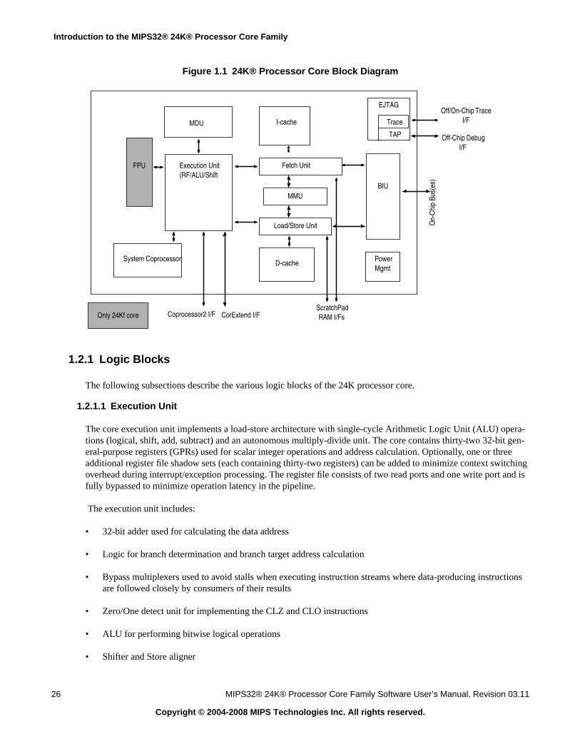
Introduction to the MIPS32® 24K® Processor Core Family
26 MIPS32® 24K® Processor Core Family Software User’s Manual, Revision 03.11
Copyright © 2004-2008 MIPS Technologies Inc. All rights reserved.
Figure 1.1 24K® Processor Core Block Diagram
1.2.1 Logic Blocks
The following subsections describe the various logic blocks of the 24K processor core.
1.2.1.1 Execution Unit
The core execution unit implements a load-store architecture with single-cycle Arithmetic Logic Unit (ALU) opera-tions (logical, shift, add, subtract) and an autonomous multiply-divide unit. The core contains thirty-two 32-bit gen-eral-purpose registers (GPRs) used for scalar integer operations and address calculation. Optionally, one or threeadditional register file shadow sets (each containing thirty-two registers) can be added to minimize context switchingoverhead during interrupt/exception processing. The register file consists of two read ports and one write port and isfully bypassed to minimize operation latency in the pipeline.
The execution unit includes:
• 32-bit adder used for calculating the data address
• Logic for branch determination and branch target address calculation
• Bypass multiplexers used to avoid stalls when executing instruction streams where data-producing instructionsare followed closely by consumers of their results
• Zero/One detect unit for implementing the CLZ and CLO instructions
• ALU for performing bitwise logical operations
• Shifter and Store aligner
Fetch Unit
MDU
MMU
D-cache
BIU
TAP
EJTAG
PowerMgmt
I-cache
Off-Chip DebugI/F
Execution Unit(RF/ALU/Shift
On-
Chi
p Bu
s(es
)
FPU
Only 24Kf core
Load/Store Unit
System Coprocessor
ScratchPadRAM I/FsCorExtend I/F Coprocessor2 I/F
Trace
Off/On-Chip TraceI/F

1.2 24K® Core Block Diagram
MIPS32® 24K® Processor Core Family Software User’s Manual, Revision 03.11 27
Copyright © 2004-2008 MIPS Technologies Inc. All rights reserved.
• Floating Point Unit Interface
• Coprocessor2 Interface
1.2.1.2 Multiply/Divide Unit (MDU)
The Multiply/Divide unit performs multiply and divide operations.The MDU consists of a pipelined 32x32 multi-plier, result-accumulation registers (HI and LO), multiply and divide state machines, and all multiplexers and controllogic required to perform these functions. This pipelined MDU supports execution of a multiply or multiply-accumu-late operation every clock cycle. Unlike previous cores, there is no dependence between operand size and issue ratefor multiplies. Divide operations are implemented with a simple 1 bit per clock iterative algorithm and require 35clock cycles in worst case to complete. Early-in to the algorithm detects sign extension of the dividend, if it is actualsize is 24, 16 or 8 bit. the divider will skip 7, 15 or 23 of the 32 iterations. An attempt to issue a subsequent MDUinstruction while a divide is still active causes a pipeline stall until the divide operation is completed.
On Pro Series cores, the MDU accumulator is accessible from the CorExtend block. Many CorExtend instructiontypes can make use of the HI/LO accumulation registers.
1.2.1.3 System Control Coprocessor (CP0)
In the MIPS architecture, CP0 is responsible for the virtual-to-physical address translation, cache protocols, theexception control system, the processor’s diagnostics capability, operating mode selection (kernel vs. user mode), andthe enabling/disabling of interrupts. Configuration information such as cache size, set associativity, and presence ofbuild-time options are available by accessing the CP0 registers. Refer to Chapter 6, “CP0 Registers of the 24K®Core” on page 146 for more information on the CP0 registers. Refer to Chapter 11, “EJTAG Debug Support in the24K® Core” on page 240 for more information on EJTAG debug registers.
1.2.1.4 Memory Management Unit (MMU)
The 24K core contains an MMU that interfaces between the execution unit and the cache controllers, shown in Figure1.2. Although the 24K core implements a 32-bit architecture, the Memory Management Unit (MMU) is modeled afterthe MMU found in the 64-bit R4000 family, as defined by the MIPS32 architecture.
On the 24K core, by default the MMU is based on a Translation Lookaside Buffer (TLB). The TLB consists of threetranslation buffers: a configurable 16/32/64 dual-entry fully associative Joint TLB (JTLB), a 4 entry fully associativeInstruction TLB (ITLB) and a 8-entry fully associative data TLB (DTLB). The ITLB and DTLB, also referred to asthe micro TLBs, are managed by the hardware and are not software visible. The micro TLBs contain subsets of theJTLB. When translating addresses, the corresponding micro TLB (I or D) is accessed first. If there is not a matchingentry, the JTLB is used to translate the address and refill the micro TLB. If the entry is not found in the JTLB, then anexception is taken.
The core optionally implements a FMT-based MMU instead of a TLB-based MMU. The FMT replaces the ITLB andDTLB and the JTLB is removed. The FMT performs a simple translation to get the physical address from the virtualaddress. Refer to Chapter 4, “Memory Management of the 24K® Core” on page 87 for more information on the FMT.
Figure 1.2 shows how the address translation mechanism interacts with cache accesses.

Introduction to the MIPS32® 24K® Processor Core Family
28 MIPS32® 24K® Processor Core Family Software User’s Manual, Revision 03.11
Copyright © 2004-2008 MIPS Technologies Inc. All rights reserved.
Figure 1.2 Address Translation During a Cache Access
1.2.1.5 Fetch Unit
The fetch unit is responsible for providing instructions to the execution unit. The fetch unit includes:
• Control logic for the instruction cache
• MIPS16e instruction recoder
• Dynamic branch prediction
• 512-entry bimodal branch history table for predicting conditional branches
• 4-entry return prediction stack for predicting return addresses
• 8-entry instruction buffer to decouple the fetch and execution pipelines
• Interface to Instruction ScratchPad RAM
1.2.1.6 Instruction Cache
The instruction cache is an on-chip memory array of up to 64 KB. The cache is virtually indexed and physicallytagged, allowing the virtual-to-physical address translation to occur in parallel with the cache access rather than hav-ing to wait for the physical address translation. The tag holds 20 or 21 bits of the physical address, a valid bit, a lockbit, and optionally a parity bit. There is a separate 6b array which holds data for all 4 ways to be used in the LeastRecently Used (LRU) replacement scheme. Some precode information is included in the instruction cache data array.An additional 6b per pair of 32b instructions is used to enable quick detection of branches and jumps in the fetch unit.If parity is implemented, a single bit covers the 6b precode and 8b cover the 64b data.
The core supports instruction cache locking. Cache locking allows critical code to be locked into the cache on a“per-line” basis, enabling the system designer to maximize the efficiency of the system cache. Cache locking is
I-cache
D-cache
Comparator
Comparator
InstructionHit/Miss
Data Hit/Miss
Virtual Address
Virtual Address
ITLB/FMT
JTLB
DTLB/FMT
InstructionAddress
Calculator
Data AddressCalculator
Entry
EntryIVA
DVA

1.2 24K® Core Block Diagram
MIPS32® 24K® Processor Core Family Software User’s Manual, Revision 03.11 29
Copyright © 2004-2008 MIPS Technologies Inc. All rights reserved.
always available on all instruction cache entries. Entries can be marked as locked or unlocked (by setting or clearingthe lock bit) on a per-entry basis using the CACHE instruction.
The LRU array must be bit-writable. The tag and data arrays only need to be word-writable.
1.2.1.7 Load/Store Unit
The Load/Store Unit is responsible for data loads and stores. It includes:
• Data cache control logic
• 4 line fill/store buffer
• ScratchPad RAM interface
1.2.1.8 Data Cache
The data cache is an on-chip memory array of up to 64 KB. The cache is virtually indexed and physically tagged,allowing the virtual-to-physical address translation to occur in parallel with the cache access. The tag holds 20 or 21bits of the physical address, a valid bit, a lock bit, and optionally a parity bit. A separate array holds the LRU bits(6b), dirty bits (4b), and optionally, dirty parity bits (4b) for all 4 ways. The data array is optionally parity protectedwith 1b per 8b of data.
In addition to instruction cache locking, all cores also support a data cache locking mechanism identical to theinstruction cache, with critical data segments to be locked into the cache on a “per-line” basis. The locked contentscannot be selected for replacement on a cache miss, but can be updated on a store hit.
Cache locking is always available on all data cache entries. Entries can be marked as locked or unlocked on aper-entry basis using the CACHE instruction.
The physical data cache memory must be byte writable to support sub-word store operations. The LRU/dirty bit arraymust be bit-writable.
1.2.1.9 Bus Interface Unit (BIU)
The Bus Interface Unit (BIU) controls the external interface signals. Additionally, it contains the implementation of acollapsing write buffer. This buffer is used to merge Write-Through transactions as well as to gather multiple writestogether from dirty line evictions and uncached accelerated stores. The write buffer consists of 4 32B entries.
1.2.1.10 Power Management
The core offers a number of power management features, including low-power design, active power management,and power-down modes of operation. The core is a static design that supports slowing or stopping the clocks toreduce power.
A register-controlled power management mode in the core provides three bits in the CP0 Status register for softwarecontrol of the power management function and allows interrupts to be serviced even when the core is in power-downmode.
An instruction-controlled power-down mode is entered by execution of the WAIT instruction and is used to invokelow-power mode.
coreRefer to Chapter 9, “Power Management in the 24K® Core” on page 232 for more information on power man-agement.

Introduction to the MIPS32® 24K® Processor Core Family
30 MIPS32® 24K® Processor Core Family Software User’s Manual, Revision 03.11
Copyright © 2004-2008 MIPS Technologies Inc. All rights reserved.
1.2.1.11 MIPS16e™ Application Specific Extension
The 24K core includes support for the MIPS16e ASE. This ASE improves code density through the use of 16-bitencodings of MIPS32 instructions plus some MIPS16e-specific instructions. PC relative loads allow quick access toconstants. Save/Restore macro instructions provide for single instruction stack frame setup/teardown for efficient sub-routine entry/exit. Sign- and zero-extend instructions improve handling of 8bit and 16bit datatypes.
A decompressor converts the MIPS16e 16-bit instructions fetched from the instruction cache or external interfaceback into 32-bit instructions for execution by the core.
Refer to the MIPS32® Architecture For Programmers, Volume IV-a: The MIPS16e™ Application-Specific Extensionto the MIPS32® Architecture [3] and to Chapter 4, “The MIPS® DSP Application-Specific Extension to theMIPS32® Instruction Set” on page 99 for more information on the features of the MIPS16e ASE.
1.2.1.12 EJTAG Debug
All cores provide basic EJTAG support with debug mode, run control, single step, and software breakpoint instruction(SDBBP) as part of the core. These features allow for the basic software debug of user and kernel code. A TAP con-troller is also included, enabling communication with an external EJTAG probe through a dedicated port. This pro-vides the possibility for debugging without debug code in the application, and for download of application code to thesystem.
An optional EJTAG feature is hardware breakpoints. A 24K core may have four instruction breakpoints and two databreakpoints, or no breakpoints. The hardware instruction breakpoints can be configured to generate a debug exceptionwhen an instruction is executed anywhere in the virtual address space. Bit mask and Address Space Identifier (ASID)values may apply in the address compare. These breakpoints are not limited to code in RAM like the software instruc-tion breakpoint (SDBBP). The data breakpoints can be configured to generate a debug exception on a data transac-tion. The data transaction may be qualified with both virtual address, data value, size and load/store transaction type.Bit mask and ASID values may apply in the address compare, and byte mask may apply in the value compare.
Another optional debug feature is support for MIPS Trace that enables real-time tracing capability. The trace infor-mation can be stored to either an on-chip trace memory or an off-chip trace probe. The trace of program flow ishighly flexible and can include the instruction program counter as well as data addresses and data values. The tracefeatures can provide a powerful software debugging mechanism.
Refer to the EJTAG Specification [11] and to Chapter 11, “EJTAG Debug Support in the 24K® Core” on page 240for more information on the EJTAG features.
1.2.1.13 CorExtend® User Defined Instructions
This optional module contains support for CorExtend user defined instructions. These instructions must be defined atbuild-time for the 24K core. The CorExtend feature is a capability of the 24Kc Pro and 24Kf Pro cores. This featuremakes 16 instructions in the opcode map available for customer usage, and each instruction can have single ormulti-cycle latency. A CorExtend instruction can operate on any one or two general-purpose registers or immediatedata contained within the instruction, and can write the result of each instruction back to a general purpose register ora local register. Implementation details for CorExtend can be found in the CorExtend® Instruction Integrator's Guidefor MIPS32® Cores [8].
Refer to Section Table 12.5 “MIPS32 SPECIAL2 Encoding of Function Field” for a specification of the opcode mapavailable for user defined instructions.

Chapter 2
MIPS32® 24K® Processor Core Family Software User’s Manual, Revision 03.11 31
Copyright © 2004-2008 MIPS Technologies Inc. All rights reserved.
Pipeline of the 24K® Core
The 24K processor core implements an 8-stage pipeline. The pipeline allows the processor to achieve high frequencywhile minimizing device complexity, reducing both cost and power consumption. This chapter contains the followingsections:
• Section 2.1 “Pipeline Stages”
• Section 2.2 “Instruction Fetch”
• Section 2.3 “Load Store Unit”
• Section 2.4 “MDU Pipeline”
• Section 2.5 “Skewed ALU”
• Section 2.6 “Interlock Handling”
• Section 2.7 “Instruction Interlocks”
• Section 2.8 “Hazards”
2.1 Pipeline Stages
The pipeline consists of eight stages:
• IF - Instruction fetch First
• IS - Instruction fetch Second
• IR - Instruction recode (MIPS16e only)
• IK - Instruction kill (MIPS16e only)
• RF - Register File
• AG - Address Generation
• EX - EXecute
• MS - Memory Second
• ER - Exception Resolution
• WB - WriteBack
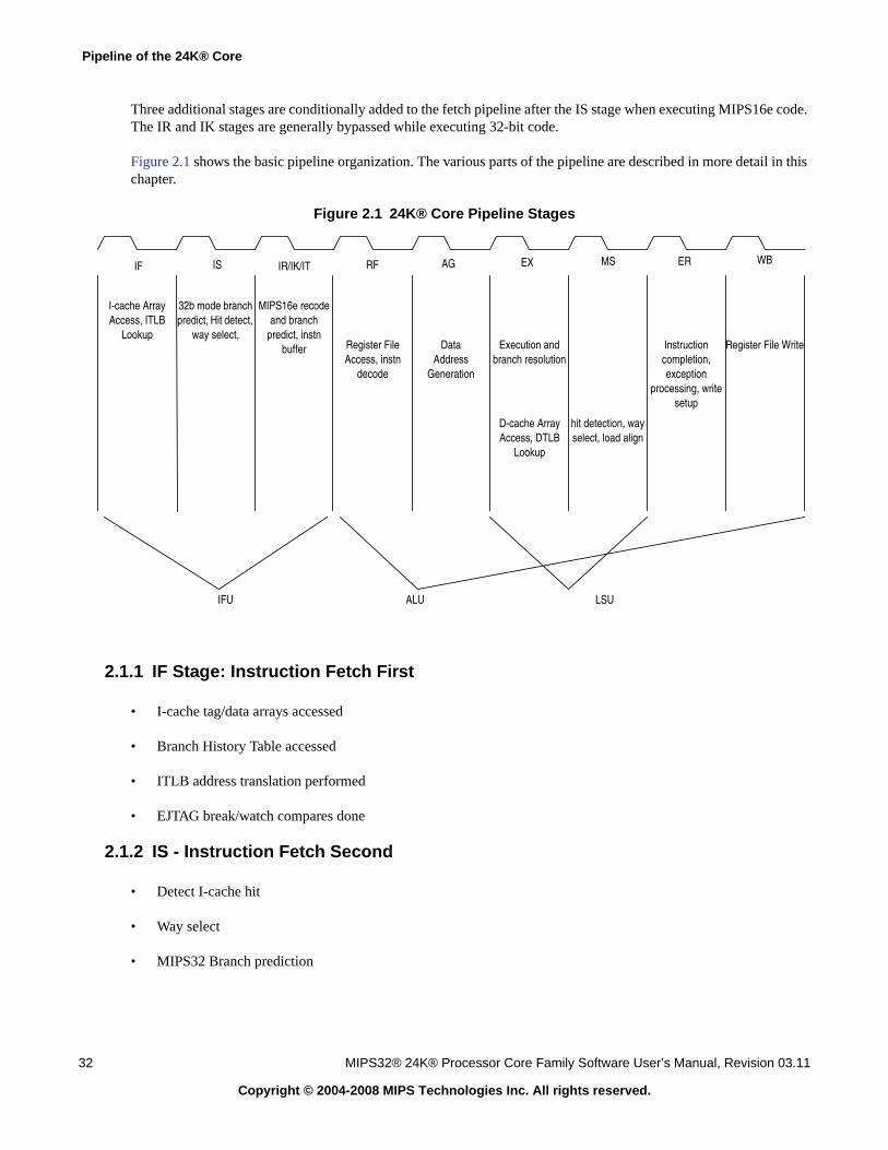
Pipeline of the 24K® Core
32 MIPS32® 24K® Processor Core Family Software User’s Manual, Revision 03.11
Copyright © 2004-2008 MIPS Technologies Inc. All rights reserved.
Three additional stages are conditionally added to the fetch pipeline after the IS stage when executing MIPS16e code.The IR and IK stages are generally bypassed while executing 32-bit code.
Figure 2.1 shows the basic pipeline organization. The various parts of the pipeline are described in more detail in thischapter.
Figure 2.1 24K® Core Pipeline Stages
2.1.1 IF Stage: Instruction Fetch First
• I-cache tag/data arrays accessed
• Branch History Table accessed
• ITLB address translation performed
• EJTAG break/watch compares done
2.1.2 IS - Instruction Fetch Second
• Detect I-cache hit
• Way select
• MIPS32 Branch prediction
IF IS IR/IK/IT RF AG EX MS ER
IFU ALU LSU
I-cache ArrayAccess, ITLB
Lookup
32b mode branchpredict, Hit detect,
way select,
MIPS16e recodeand branch
predict, instnbuffer Register File
Access, instndecode
DataAddress
Generation
Execution andbranch resolution
Instructioncompletion,exception
processing, writesetup
D-cache ArrayAccess, DTLB
Lookup
hit detection, wayselect, load align
Register File Write
WB

2.1 Pipeline Stages
MIPS32® 24K® Processor Core Family Software User’s Manual, Revision 03.11 33
Copyright © 2004-2008 MIPS Technologies Inc. All rights reserved.
2.1.3 IR - Instruction Recode (MIPS16e only)
• MIPS16 recode
• MIPS16 branch prediction
• Stage is bypassed when executing MIPS32 code
2.1.4 IK - Instruction Kill (MIPS16e only)
• Kill MIPS16 instructions (due to branches as an example)
• Stage is bypassed when executing MIPS32 code
2.1.5 IT - Instruction Fetch Third
• Stage is bypassed when executing MIPS32 code and the instruction buffer is empty
• Instruction Buffer
• Branch target calculation
2.1.6 RF - Register File Access
• Register File access
• Instruction decoding/dispatch logic
• Bypass muxes
2.1.7 AG - Address Generation
• D-cache Address Generation
• Bypass muxes
2.1.8 EX - Execute/Memory Access
• Skewed ALU
• DTLB
• Start DCache access
• Branch Resolution
2.1.9 MS - Memory Access Second
• Complete DCache access
• DCache hit detection

Pipeline of the 24K® Core
34 MIPS32® 24K® Processor Core Family Software User’s Manual, Revision 03.11
Copyright © 2004-2008 MIPS Technologies Inc. All rights reserved.
• Way select mux
• Load align
2.1.10 ER- Exception Resolution
• Instruction completion
• Register file write setup
• Exception processing
2.1.11 WB - Writeback
• Register file writeback occurs on rising edge of this cycle
2.2 Instruction Fetch
The IFU is responsible for supplying instructions to the execution units and handling the results of all control transferinstructions (branches, jumps, etc.). The IFU operation encompasses four pipe stages: IF (Instruction fetch First), IS(Instruction fetch Second), IR (Instruction Recode) and IK (Instruction Kill). The instruction cache tags and data areaccessed in IF, and the hit determination and the first part of the 32-bit mode target calculation is done in IS. The IRand IK stage handle MIPS16e recoding. The remainder of the 32-bit mode target calculation as well as instructionbuffering to the ALU is done in the IT stage, but can be bypassed during 32-bit mode if the instruction buffer isempty. This instruction buffering decouples the IFU from the rest of the pipeline, allowing fetches to proceed even ifthe processor execution is stalled for some reason. The fetch pipeline and cache bandwidth is 64 bits, supplying up totwo instructions per cycle in MIPS32 mode, which allows the IFU to get ahead of the ALU and shields the executionpipeline from some IFU miss penalties.
Figure 2.2 shows the general datapath of the IFU along with major structures.
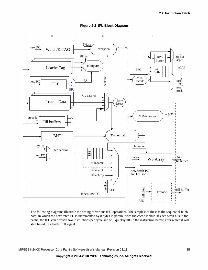
2.2 Instruction Fetch
MIPS32® 24K® Processor Core Family Software User’s Manual, Revision 03.11 35
Copyright © 2004-2008 MIPS Technologies Inc. All rights reserved.
Figure 2.2 IFU Block Diagram
The following diagrams illustrate the timing of various IFU operations. The simplest of these is the sequential fetchpath, in which the next fetch PC is incremented by 8 bytes in parallel with the cache lookup. If each fetch hits in thecache, the IFU can provide two instructions per cycle and will quickly fill up the instruction buffer, after which it willstall based on a buffer full signal.
IF IS IT
I-cache Tag
I-cache Data
Fill buffers
ITLB
compare
BHT Target calc.
PA
bank
hit
71b data x5
M16recode
RPS
ALUredi
rect
M16 target calc.to mux
M16 target
new PC
Watch/EJTAGnew PC exception
to ITLB etc.
Precode
BIU
to fill buffer
new fetch PC
index/low PC
$ data
precode
new PC
+2/4/8sequential
resume PC
inst.,EPC,exc.,pred.
exc. tag
fill buf
fill d
ata
Inst.Buffer
EPC
Earlydecode
BIU
RPSBuffer
RPS
ALU
JR $31target
WS Arrayindex
hit/miss
way
to fill buffer
fill/cacheop

Pipeline of the 24K® Core
36 MIPS32® 24K® Processor Core Family Software User’s Manual, Revision 03.11
Copyright © 2004-2008 MIPS Technologies Inc. All rights reserved.
Figure 2.3 Timing of 32-bit Mode Sequential Fetches
Another common situation is a control transfer instruction (branch/jump). The calculation of the target for 32-bitmode instructions starts in the IS stage, but does not complete until the IT stage. For a predicted taken path this meansthat if the delay slot of that branch is in the same fetch bundle, there will be a 2 cycle bubble since the sequentialfetches will not be used. If the delay slot is in the next fetch bundle, there will be a 1 cycle bubble.
Figure 2.4 Timing of 32-bit Mode Branch Taken Path
For conditional branches, the control transfer is most likely speculative, based upon the branch history table. The res-olution of this branch by the ALU will be calculated in the EX stage and will be used by the IFU in the MS stage,resulting in a several-cycle fetch bubble. The following figure illustrates one possibility assuming the instructionbuffer is empty and the delay slot is in the same fetch bundle.
PC+8
PC+8
. . .
. . .
. . .
Two inst/cycle
IF IS IT
IF IS IT
. . .
IF IS IT
IF IS IT
. . .
IF IS IT
IF IS IT
. . .
PC+8
target
predicted takenIF IS IT
IF IS IT
IF
IF
branch
delay slot. . .
killed
. . .. . .IF IS IT
IF IS IT
IF
IF
PC+8killed
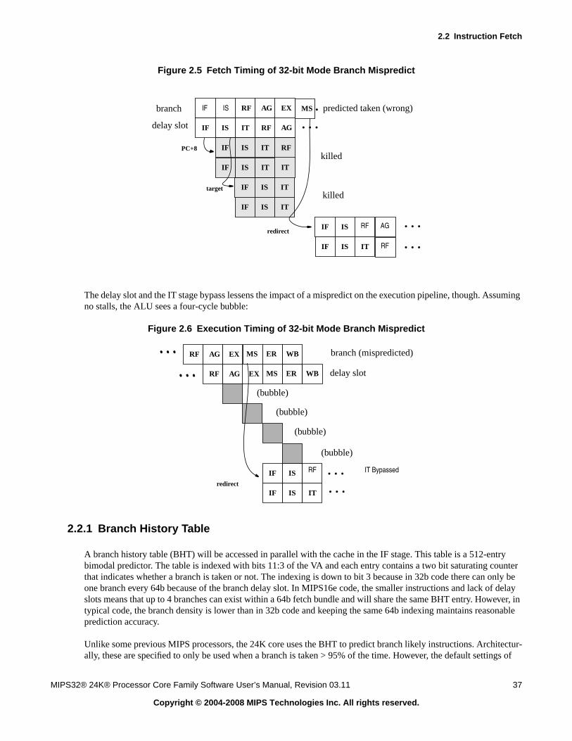
2.2 Instruction Fetch
MIPS32® 24K® Processor Core Family Software User’s Manual, Revision 03.11 37
Copyright © 2004-2008 MIPS Technologies Inc. All rights reserved.
Figure 2.5 Fetch Timing of 32-bit Mode Branch Mispredict
The delay slot and the IT stage bypass lessens the impact of a mispredict on the execution pipeline, though. Assumingno stalls, the ALU sees a four-cycle bubble:
Figure 2.6 Execution Timing of 32-bit Mode Branch Mispredict
2.2.1 Branch History Table
A branch history table (BHT) will be accessed in parallel with the cache in the IF stage. This table is a 512-entrybimodal predictor. The table is indexed with bits 11:3 of the VA and each entry contains a two bit saturating counterthat indicates whether a branch is taken or not. The indexing is down to bit 3 because in 32b code there can only beone branch every 64b because of the branch delay slot. In MIPS16e code, the smaller instructions and lack of delayslots means that up to 4 branches can exist within a 64b fetch bundle and will share the same BHT entry. However, intypical code, the branch density is lower than in 32b code and keeping the same 64b indexing maintains reasonableprediction accuracy.
Unlike some previous MIPS processors, the 24K core uses the BHT to predict branch likely instructions. Architectur-ally, these are specified to only be used when a branch is taken > 95% of the time. However, the default settings of
AG
EX
RF
IT
PC+8
. . .
killed
redirect
predicted taken (wrong)
. . .
. . .
RF
IF IS IT
. . .
IF IS IT
IF IS IT
AG
RF
. . .. . .
IF IS
IF IS IT
. . .branch
delay slot
. . .
IF IS IT
IF IS IT
targetkilled
IF IS
RF AG
RF
MS
. . .
redirect
branch (mispredicted)
. . .
delay slot
(bubble)
(bubble)
. . .
. . .
IF IS
IF IS IT
RF AG EX MS ER
RF AG EX MS ER
. . .
. . .
. . . WB
WB
(bubble)
(bubble)
RF IT Bypassed

Pipeline of the 24K® Core
38 MIPS32® 24K® Processor Core Family Software User’s Manual, Revision 03.11
Copyright © 2004-2008 MIPS Technologies Inc. All rights reserved.
many compilers use these even when that is not the case. The delay slot characteristics (the delay slot is only executedif the branch is taken) allow a useful instruction to be placed in the delay slot instead of a NOP. When used in thisfashion, dynamic prediction is much more accurate than statically predicting a branch likely as taken.
Unconditional branches (BEQ r0, r0 and BGEZAL r0) are detected by the precode logic and will be statically pre-dicted taken, bypassing the BHT.
The ALU verifies the correctness of the prediction when the branch reaches the EX stage. In the case of a mispredict,the instructions on the mispredicted path will be killed and the fetch will be redirected to the correct instruction. Thiswill cause a 4 cycle bubble in the pipeline.
2.2.1.1 Branch Target Calculation
Branch target calculation is done in the IT stage. This alleviates a critical timing path in the IFU and removes the needfor replicating the branch target logic on all 4 ways of the cache. In the case of a jump or a branch that is predictedtaken, subsequent fetches will be killed (after the fetch of the delay slot). This added cycle is generally covered by theinstruction buffer. A string of taken branches will slowly drain the instruction buffer as only two instructions arefetched every three cycles.
2.2.2 Return Prediction Stack
The return prediction stack (RPS) is a simple stack to hold return addresses. Every time a JAL, JALR ra, or BGEZALis seen, the link address is pushed onto the stack. When a JR ra is executed, a link address is popped off of the stack.If calling convention is maintained and the stack doesn’t overflow, this will have very high prediction accuracy. TheRPS contains 4 entries.
The ALU will verify the correctness of the prediction in the EX stage. If the prediction was wrong, the fetch will beredirected in the MS stage and there will be a 4 cycle bubble from the misprediction.
JR that don’t use ra are not predicted. The IFU will stall until the ALU reads the register file. The timing on this willbe the same as for a return mispredict.
2.2.3 ITLB
The IFU relies on a small subset of TLB entries stored locally in a four-entry ITLB to translate the PC into a physicaladdress for tag comparison. The ITLB stores mappings for 4KB or 1MB pages or sub-pages (i.e. if the JTLB page is64KB, only the 4KB sub-page containing the desired virtual address will be mapped into the ITLB). The ITLB accessoccurs in parallel with the primary cache lookup. If there is a miss in the ITLB, the BIU must look up the entry in themain JTLB.
A miss in the ITLB will be detected in the IF stage, and the IFU will kill that fetch. The virtual address and the missindication will be sent to the BIU during IF, allowing the JTLB to start a lookup in the next cycle. The latency of theJTLB lookup can be impacted by several factors. The JTLB can be busy processing a DTLB miss or a TLB operation,delaying the start of the JTLB lookup. Also, the JTLB access time depends on how it is implemented. AnSRAM-based PFN array will take an extra cycle over a flop-based version, yielding a 3 cycle latency instead of 2. Thefetch will be restarted when the JTLB indicates that data is going to be returned.
The cache coherence attributes can be reduced to one bit (uncached/cached) for the instruction cache. An ITLB entrywill also record the associated JTLB entry, so that for a JTLB write, the ITLB can invalidate its copy if present. TheITLB uses a true LRU replacement algorithm.
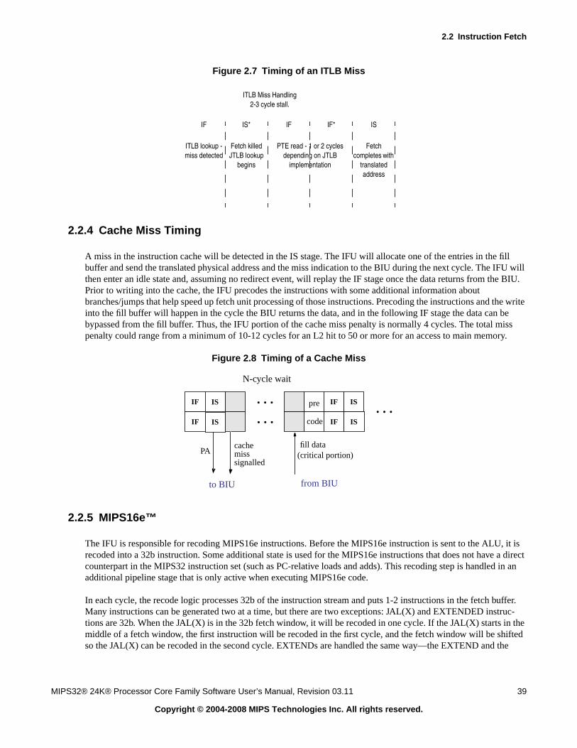
2.2 Instruction Fetch
MIPS32® 24K® Processor Core Family Software User’s Manual, Revision 03.11 39
Copyright © 2004-2008 MIPS Technologies Inc. All rights reserved.
Figure 2.7 Timing of an ITLB Miss
2.2.4 Cache Miss Timing
A miss in the instruction cache will be detected in the IS stage. The IFU will allocate one of the entries in the fillbuffer and send the translated physical address and the miss indication to the BIU during the next cycle. The IFU willthen enter an idle state and, assuming no redirect event, will replay the IF stage once the data returns from the BIU.Prior to writing into the cache, the IFU precodes the instructions with some additional information aboutbranches/jumps that help speed up fetch unit processing of those instructions. Precoding the instructions and the writeinto the fill buffer will happen in the cycle the BIU returns the data, and in the following IF stage the data can bebypassed from the fill buffer. Thus, the IFU portion of the cache miss penalty is normally 4 cycles. The total misspenalty could range from a minimum of 10-12 cycles for an L2 hit to 50 or more for an access to main memory.
Figure 2.8 Timing of a Cache Miss
2.2.5 MIPS16e™
The IFU is responsible for recoding MIPS16e instructions. Before the MIPS16e instruction is sent to the ALU, it isrecoded into a 32b instruction. Some additional state is used for the MIPS16e instructions that does not have a directcounterpart in the MIPS32 instruction set (such as PC-relative loads and adds). This recoding step is handled in anadditional pipeline stage that is only active when executing MIPS16e code.
In each cycle, the recode logic processes 32b of the instruction stream and puts 1-2 instructions in the fetch buffer.Many instructions can be generated two at a time, but there are two exceptions: JAL(X) and EXTENDED instruc-tions are 32b. When the JAL(X) is in the 32b fetch window, it will be recoded in one cycle. If the JAL(X) starts in themiddle of a fetch window, the first instruction will be recoded in the first cycle, and the fetch window will be shiftedso the JAL(X) can be recoded in the second cycle. EXTENDs are handled the same way—the EXTEND and the
IF IS* IF IF* IS
ITLB lookup -miss detected
Fetchcompletes with
translatedaddress
PTE read - 1 or 2 cyclesdepending on JTLB
implementation
Fetch killedJTLB lookup
begins
ITLB Miss Handling2-3 cycle stall.
IF IF IS
IF IF IS
. . .
PAcache fill data
to BIU from BIU
N-cycle wait
pre
code
(critical portion)
. . .
. . .IS
IS
misssignalled
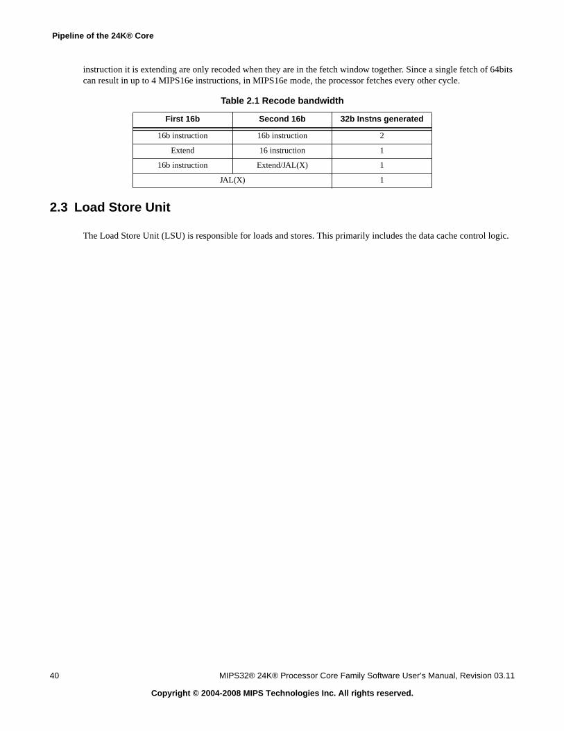
Pipeline of the 24K® Core
40 MIPS32® 24K® Processor Core Family Software User’s Manual, Revision 03.11
Copyright © 2004-2008 MIPS Technologies Inc. All rights reserved.
instruction it is extending are only recoded when they are in the fetch window together. Since a single fetch of 64bitscan result in up to 4 MIPS16e instructions, in MIPS16e mode, the processor fetches every other cycle.
2.3 Load Store Unit
The Load Store Unit (LSU) is responsible for loads and stores. This primarily includes the data cache control logic.
Table 2.1 Recode bandwidth
First 16b Second 16b 32b Instns generated
16b instruction 16b instruction 2
Extend 16 instruction 1
16b instruction Extend/JAL(X) 1
JAL(X) 1
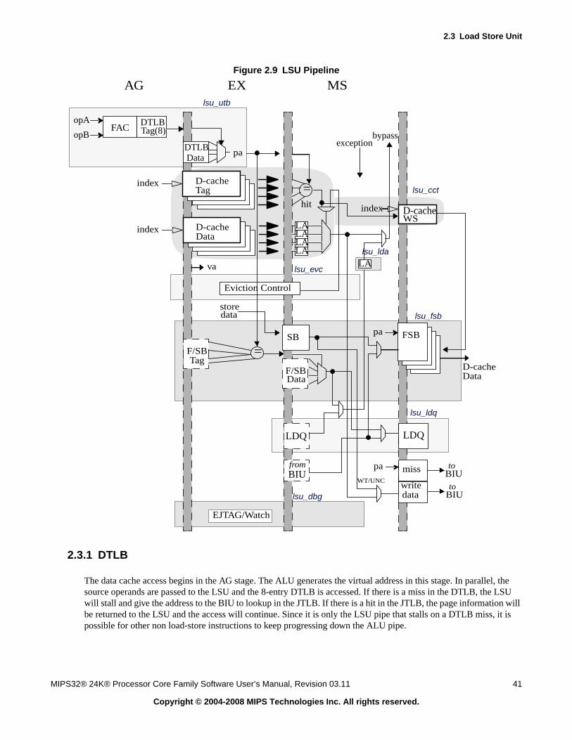
2.3 Load Store Unit
MIPS32® 24K® Processor Core Family Software User’s Manual, Revision 03.11 41
Copyright © 2004-2008 MIPS Technologies Inc. All rights reserved.
Figure 2.9 LSU Pipeline
2.3.1 DTLB
The data cache access begins in the AG stage. The ALU generates the virtual address in this stage. In parallel, thesource operands are passed to the LSU and the 8-entry DTLB is accessed. If there is a miss in the DTLB, the LSUwill stall and give the address to the BIU to lookup in the JTLB. If there is a hit in the JTLB, the page information willbe returned to the LSU and the access will continue. Since it is only the LSU pipe that stalls on a DTLB miss, it ispossible for other non load-store instructions to keep progressing down the ALU pipe.
EJTAG/Watch
D-cacheindex
D-cacheindex
pa
=hit
MS
D-cacheindex
FSBSB
storedata
D-cache
F/SB
EXAG
FACDTLBopA
opB
Tag=
F/SBData
Tag(8)
DTLBData
bypass
LDQLDQ
LALALALA
LA
BIUfrom miss to
BIUpa
va
lsu_utb
lsu_cct
lsu_fsb
lsu_ldq
writedata
pa
toBIU
Eviction Control
lsu_evc
lsu_dbg
exception
lsu_lda
WT/UNC
Tag
Data
WS
Data

Pipeline of the 24K® Core
42 MIPS32® 24K® Processor Core Family Software User’s Manual, Revision 03.11
Copyright © 2004-2008 MIPS Technologies Inc. All rights reserved.
Figure 2.10 DTLB Miss Timing
The DTLB will only store mappings either for 4K or 1M pages or subpages of a larger JTLB entry. A DTLB entrywill also record the associated JTLB entry, so that for a JTLB write, the DTLB can invalidate its copy if present. TheDTLB uses a pseudo-LRU replacement algorithm. If the Fixed Mapping MMU is used instead of a TLB, the addresstranslation will be done in the EX stage, and there will never be a DTLB miss.
2.3.2 Data Cache Access
The data cache access is done during the EX stage. The tag and data arrays are accessed and the values are saved inflops for use in the MS stage. In parallel with the array lookup (in EX), the physical address is used to do an early tagcompare on entries in the Fill Store Buffer (FSB) and Store Buffer (SB).
The SB is a single entry buffer that is used to stage store data into the other structures. It is fully bypass-able, allowinga load immediately after a store to the same address to execute without stalls. From the SB, the store data will moveinto the FSB if the store hits in the cache or it is an allocating miss. The store data is then written into the cache oppor-tunistically.
During the MS stage, the data cache tags are compared to the physical address to determine whether a reference hit inthe cache or not. If there is a hit, the way select (WS) array will be written to mark the most recently used way, andload data will be bypassed back to the ALU. On a cache miss, an FSB entry is allocated to hold the fill data as itreturns from the BIU. The WS array is read and the replacement way is determined. If the line selected for replace-ment is dirty, an eviction will begin and the dirty data will be written back to memory. A load miss will also allocatean entry in the Load Queue (LDQ). This buffer is used to hold the aligned load data while it is being staged back intothe ALU.
The core portion of a load miss is shown in Figure 2.11. It takes one cycle to get from the LSU through the BIU andout onto the OCP bus. It takes at least 1 cycle for the data to be returned. Then 2 more cycles are required to get thedata back to the ALU.
AG EX* EX* EX* EX
DTLB lookup -miss detected
LSU p iperestarts withtranslatedaddress
PTE read - 1 or 2 cyclesdepending on JTLB
implementation
Pipe StallsAddress sent to
JTLB forlookup
DTLB Miss Handling2-3 cycle lsu pipe stall.

2.4 MDU Pipeline
MIPS32® 24K® Processor Core Family Software User’s Manual, Revision 03.11 43
Copyright © 2004-2008 MIPS Technologies Inc. All rights reserved.
Figure 2.11 Cache Miss Timing
2.3.3 Outstanding misses
The 24K core features non-blocking D-cache misses. In the cases where the following instructions are not dependenton the load data, the core can continue executing instructions while the miss is being processed. The core can handlemultiple outstanding misses.
• Up to 8 independent cache lines - this includes cache refills requested for loads, stores, and prefetches as well assingle uncached load requests. Multiple cacheable requests to the same line can be merged. This limit is depen-dent on the number of Fill-Store Buffer (FSB) entries the core is configured with.
• Up to 9 load misses - Up to 9 separate loads can be outstanding. The loads can be to different cache lines or mul-tiple loads can be to the same cache line. This limit is dependent on the number of Load Data Queue (LDQ)entries the core was built with.
2.3.4 Uncached Accesses
Uncached accesses are handled similarly to cached accesses. The cacheability of the reference is not known until theaddress translation has completed in the EX stage, so the cache access is performed anyway. On an uncached refer-ence, a miss will be forced. Uncached loads will request the exact amount of data required and allocate an FSB andLDQ entry. Uncached loads are non-blocking just like cached misses. Uncached stores will be sent to the BIU.
To the LSU, uncached accelerated stores look the same as uncached stores. In the BIU, however, they are handleddifferently—the BIU will attempt to gather uncached accelerated stores and do a bursted write to improve bus effi-ciency.
2.4 MDU Pipeline
The autonomous multiply/divide unit (MDU) has a separate pipeline for multiply and divide operations. This pipelineoperates in parallel with the integer unit (ALU) pipeline and does not stall when the ALU pipeline stalls. This allowsmulti-cycle MDU operations, such as a divide, to be partially masked by system stalls and/or other integer unitinstructions.
The MDU consists of a 32x32 booth recoded multiplier array, separate carry-lookahead adders for multiply anddivide, result/accumulation registers (HI and LO), multiply and divide state machines, and all necessary multiplexersand control logic.
MS
loadmiss
to BIURequestQueue
OCP
- - - -
BIU LDQ
to pipe
1 2x

Pipeline of the 24K® Core
44 MIPS32® 24K® Processor Core Family Software User’s Manual, Revision 03.11
Copyright © 2004-2008 MIPS Technologies Inc. All rights reserved.
The MDU supports execution of a multiply operation every clock cycle. Divide operations are implemented with asimple 1 bit per clock iterative algorithm with an early in detection of sign extension on the dividend (rs). An attemptto issue a subsequent MDU instruction which would access the HI or LO register before the divide completes causes adelay in starting the subsequent MDU instruction. Some concurrency is enabled by the separate adders for the multi-ply and divide data paths. The MDU instruction may start executing once the divide is ensured of writing to the HIand LO registers before the MDU instruction will access them. A MUL instruction, which does not access the HI orLO register, may start executing anytime relative to a previous divide instruction.
Table 2.2 lists the delays (number of cycles until a result is available) for multiply and divide instructions. The delaysare listed in terms of pipeline clocks. In this table ‘delay’ refers to the number of cycles the pipeline must stall the sec-ond instruction to wait for the result of the first instruction.
In Table 2.2 a delay of zero means that the first and second instructions can be issued back to back in the code withoutthe MDU causing any stalls in the ALU pipeline. A delay of one means that if issued back to back, the ALU pipelinewill be stalled for one cycle.
Table 2.2 MDU Instruction Delays
Size of Operand
1st Instruction[1]
Instruction SequenceDelay
Clocks1st Instruction 2nd Instruction
32 bit MULT/MULTU,MADD/MADDU, or
MSUB/MSUBU
MADD/MADDU,MSUB/MSUBU, or MFHI/MFLO
0
32 bit MUL Integer operation[1] 4
8 bit DIVU MFHI/MFLO 7
16 bit DIVU MFHI/MFLO 15
24 bit DIVU MFHI/MFLO 23
32 bit DIVU MFHI/MFLO 31
8 bit DIV MFHI/MFLO 9[2]
16 bit DIV MFHI/MFLO 17[2]
24 bit DIV MFHI/MFLO 25[2]
32 bit DIV MFHI/MFLO 33[2]
any MFHI/MFLO Integer operation[1] 4
any MTHI/MTLO MADD/MADDU,MSUB/MSUBU
1
any MTHI/MTLO MFHI/MFLO 0
[1] Integer Operation refers to any integer instruction that uses the result of a previous MDU operation.[2] If both operands are positive, then the two Sign Adjust stages are bypassed. Delay is then the same as
for DIVU.
Table 2.3 Multiply Instruction (updating HI/LO) Repeat Rates
Instruction SequenceRepeat
Rate1st Instruction 2nd Instruction
MULT/MULTU,MADD/MADDU,MSUB/MSUBU
MADD/MADDU,MSUB/MSUBU
1

2.4 MDU Pipeline
MIPS32® 24K® Processor Core Family Software User’s Manual, Revision 03.11 45
Copyright © 2004-2008 MIPS Technologies Inc. All rights reserved.
The repeat rate of 1 for MULT/MULTU/MADD/MADDU/MSUB/MSUBU to MADD/MADDU/MSUB/MSUBUare achieved by feeding the result of the M3MDU stage for the first instruction back into the M3MDU stage for the sec-ond instruction.
2.4.1 Multiply Pipeline Stages
The multiply operation begins in BMDU stage, which would be the EX stage in the integer pipeline. The booth recod-ing function occurs at this time. The multiply calculation requires three clocks and occurs in the M1MDU, M2MDU,and M3MDU stages. The carry-lookahead-add (CLA) function occurs at the end of the M3MDU stage. In the AMDU
stage, the result is selected from the multiply data path, HI register, and LO register to be returned to the ALU for theMFHI, MFLO, and MUL instructions. If the MDU instruction is not one of these, the result is selected to be writteninto the HI/LO registers instead. The result is ready to be read from the HI/LO registers in the WMDU stage.
The following figures illustrate a multiply (accumulate) instruction and the interaction with the main integer pipeline.These figures are applicable to MUL, MULT, MULTU, MADD, MADDU, MSUB, and MSUBU instructions
Figure 2.12 Multiply Pipeline
Figure 2.13 Multiply With Dependency From ALU
Table 2.4 MUL Repeat Rates
Instruction SequenceRepeat
Rate1st Instruction 2nd Instruction
MUL MUL (no data dependency) 1-3[1,2]
[1] There is no data dependency between first and second MUL. Otherwise, therepeat rate is the same as for MUL to integer operations in Figure 2.2
[2] MULs can be issued at the maximum rate of 3 every 5 cycles. Three can beissued back to back, but a fourth one would stall.
RF BMDU M1MDU M2MDU AMDU WMDUAG
(EX)
M3MDU
Result bypassRF EXAG
RF BMDU M1MDU M2MDU AMDU WMDUAG M3MDU
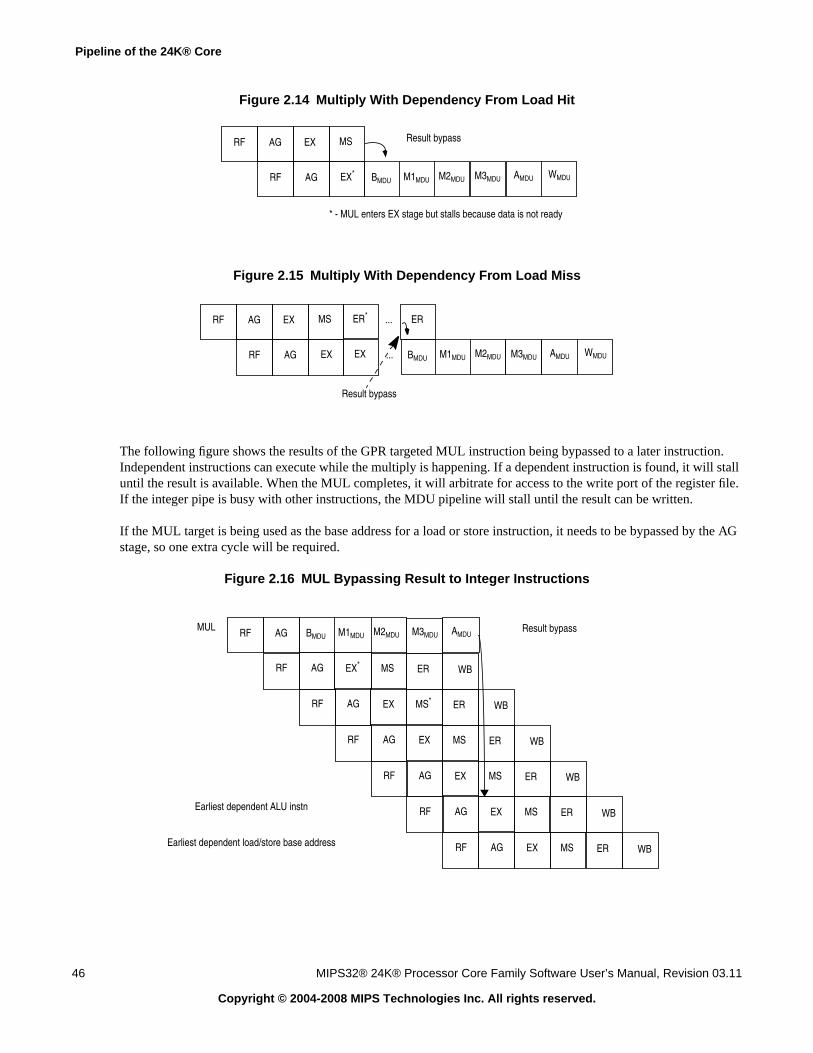
Pipeline of the 24K® Core
46 MIPS32® 24K® Processor Core Family Software User’s Manual, Revision 03.11
Copyright © 2004-2008 MIPS Technologies Inc. All rights reserved.
Figure 2.14 Multiply With Dependency From Load Hit
Figure 2.15 Multiply With Dependency From Load Miss
The following figure shows the results of the GPR targeted MUL instruction being bypassed to a later instruction.Independent instructions can execute while the multiply is happening. If a dependent instruction is found, it will stalluntil the result is available. When the MUL completes, it will arbitrate for access to the write port of the register file.If the integer pipe is busy with other instructions, the MDU pipeline will stall until the result can be written.
If the MUL target is being used as the base address for a load or store instruction, it needs to be bypassed by the AGstage, so one extra cycle will be required.
Figure 2.16 MUL Bypassing Result to Integer Instructions
RF BMDU M1MDU M2MDU AMDU WMDUAG
RF EXAG MS
EX*
Result bypass
M3MDU
* - MUL enters EX stage but stalls because data is not ready
RF BMDU M1MDU M2MDU AMDU WMDUAG
RF EXAG MS
EX
...ER*
EX ...
ER
Result bypass
M3MDU
RF BMDU M1MDU M2MDU AMDUAG
RF AG EX* MS ER
Result bypassM3MDU
WB
RF AG EX MS* ER WB
RF AG EX MS ER WB
RF AG EX MS ER WB
RF AG EX MS ER WB
RF AG EX MS ER WB
MUL
Earliest dependent ALU instn
Earliest dependent load/store base address

2.4 MDU Pipeline
MIPS32® 24K® Processor Core Family Software User’s Manual, Revision 03.11 47
Copyright © 2004-2008 MIPS Technologies Inc. All rights reserved.
2.4.2 Divide Operations
Divide operations are implemented using a simple non-restoring division algorithm. This algorithm works only forpositive operands, hence the first cycle of the MMDU stage is used to negate the rs operand (RS Adjust) if needed. Notethat this cycle is spent even if the adjustment is not necessary. In cycle 2, the first add/subtract iteration is executed. Incycle 3 an early-in detection is performed. The adjusted rs operand is detected to be zero extended on the upper most8, 16 or 24 bits. If this is the case the following 7, 15 or 23 cycles of the add/subtract iterations are skipped. Duringthe next maximum 31 cycles (4-34), the remaining iterative add/subtract loop is executed.
The remainder adjust (Rem Adjust) cycle is required if the remainder was negative. Note that this cycle is spent evenif the remainder was positive. A sign adjust is performed on the quotient and/or remainder if necessary. The signadjust stages are skipped if both operands are positive.
Figure 2.17, Figure 2.18, Figure 2.19 and Figure 2.20 show the worst case latencies for 8, 16, 24 and 32 bit divideoperations, respectively. The worst case repeat rate is either 14, 22, 30 or 38 cycles (two less if the sign adjust stage isskipped).
Figure 2.17 MDU Pipeline Flow During a 8-bit Divide (DIV) Operation
Figure 2.18 MDU Pipeline Flow During a 16-bit Divide (DIV) Operation
Figure 2.19 MDU Pipeline Flow During a 24-bit Divide (DIV) Operation
RS Adjust
IDLE Stage ERLY Stage DIV Stages RMD Stage
Add/SubtraceEarly In
Clock 1 3 4-10 11
SGN Stage
12
Rem. Adjust
DIV1 Stage
Add/Subtract
2
Sign Adjust 1
SGN2 Stage
13
Sign Adjust 2
IDLE Stage
14
Result Ready
RS Adjust
IDLE Stage ERLY Stage DIV Stages RMD Stage
Add/SubtraceEarly In
Clock 1 3 4-18 19
SGN Stage
20
Rem. Adjust
DIV1 Stage
Add/Subtract
2
Sign Adjust 1
SGN2 Stage
21
Sign Adjust 2
IDLE Stage
22
Result Ready
RS Adjust
IDLE Stage ERLY Stage DIV Stages RMD Stage
Add/SubtraceEarly In
Clock 1 3 4-26 27
SGN Stage
28
Rem. Adjust
DIV1 Stage
Add/Subtract
2
Sign Adjust 1
SGN2 Stage
29
Sign Adjust 2
IDLE Stage
30
Result Ready

Pipeline of the 24K® Core
48 MIPS32® 24K® Processor Core Family Software User’s Manual, Revision 03.11
Copyright © 2004-2008 MIPS Technologies Inc. All rights reserved.
Figure 2.20 MDU Pipeline Flow During a 32-bit Divide (DIV) Operation
2.5 Skewed ALU
The 24K core has a skewed ALU. This is referring to the fact that the ALU is located in the EX stage instead of theAG stage. This allows the load to use delay to be two cycles, the same as it was in the shorter 4KE pipeline. Softwareoptimized for that pipeline can run without incurring additional stalls. Of course, this does not come for free - anALU instruction generating the base address for a load or store will have an additional cycle stall. Independent of theALU location, pointer chasing loads (loads generating the base address for following loads) will see the full 3 cyclesof cache access time.
This is shown in Figure 2.21. The earliest an ALU consumer of load data can issue is two cycles after the load. Theearliest a load/store consumer can issue is three cycles after the load.
The bypass of data from the ALU is shown in Figure 2.22. For back to back ALU instructions, the result is bypassedfrom the EX stage to the AG stage. For an ALU bypassing to the base address register of a load or store, the bypass-ing is from the EX stage to the RF stage and the load cannot issue until two cycles after the ALU instruction. Notethat the data register for a store is not used in the AG stage and a dependency there will look like the ALU to ALUbypass.
Figure 2.21 Load Data Bypass
RS Adjust
IDLE Stage ERLY Stage DIV Stages RMD Stage
Add/SubtraceEarly In
Clock 1 3 4-34 35
SGN Stage
36
Rem. Adjust
DIV1 Stage
Add/Subtract
2
Sign Adjust 1
SGN2 Stage
37
Sign Adjust 2
IDLE Stage
38
Result Ready
One Cycle One Cycle One Cycle One Cycle One Cycle One Cycle
RF AG EX MS ER
RF AG EX MS ER
RF AG EX MS
Load Instruction
ALU Consumer of Load Data Instruction
Data bypass from MS to AG/RF
RF AG EXLoad/Store Consumer of Load Data Instruction

2.6 Interlock Handling
MIPS32® 24K® Processor Core Family Software User’s Manual, Revision 03.11 49
Copyright © 2004-2008 MIPS Technologies Inc. All rights reserved.
Figure 2.22 ALU Data Bypass
2.6 Interlock Handling
Smooth pipeline flow is interrupted when cache misses occur or when data dependencies are detected. Interruptionshandled entirely in hardware, such as cache misses, are referred to as interlocks. At each cycle, interlock conditionsare checked for all active instructions.
Table 2.5 lists the types of pipeline interlocks for the 24K processor core.
Table 2.5 Pipeline Interlocks
Interlock Type Sources Slip Stage
GPR dependency - load/store address Dest. register for any instruction in previ-ous cycle
AG
Dest. register for loads/MFCx/MDU instnsin previous 2 cycles
MDU busy Previous MDU operation not completed AG
GPR dependency Dest. register for loads/MFCx/MDU instnsin previous cycle
EX
LDQ full Load in pipe while Load Queue is full
Blocking load bubble Blocking load immediately followinganother blocking load
SYNC, I-Cache Previous I-Cache not completed
One Cycle One Cycle One Cycle One Cycle One Cycle One Cycle
RF AG EX MS ER
RF AG EX MS ER
RF AG EX MS
ALU Instruction
ALU Consumer of ALU Data
Data bypass from EX to AG/RF
Load/Store Consumer of ALU Data

Pipeline of the 24K® Core
50 MIPS32® 24K® Processor Core Family Software User’s Manual, Revision 03.11
Copyright © 2004-2008 MIPS Technologies Inc. All rights reserved.
2.7 Instruction Interlocks
Most instructions can be issued at a rate of one per clock cycle. In order to adhere to the sequential programmingmodel, the issue of an instruction must sometimes be delayed. This to ensure that the result of a prior instruction isavailable. Table 2.6 details the instruction interactions that prevent an instruction from advancing in the processorpipeline.
Destination GPR dependency Outstanding GPR write to same register MS
WBB full Store/CACHE instn in pipe while Write-back Buffer is full
SPRAM busy SPRAM load/store in pipe while SPRAMis busy
FSB flush SYNC/CACHE/load/store instn requiresFill Store Buffer to be flushed
DTLB miss Load/Store address miss in microTLB
CACHE CACHE instn needs to re-access data cache
L2 CACHE Previous L2 CACHE not completed
Blocking load miss Load misses with non-blocking loads dis-abled
ER
Table 2.6 Instruction Interlocks
Instruction Interlocks
First Instruction Second InstructionIssue Delay (inClock Cycles) Slip Stage
LB/LBU/LH/LHU/LL/LW/LWL/LWR
ALU Consumer of load data 1 EX stage
Load/Store consumer for baseaddress register
2 AG stage
MFC0 ALU consumer of destinationregister
2 EX stage
Load/store consumer for baseaddress
3 AG stage
MULTx/MADDx/MSUBx MFLO/MFHI 0
MUL/MFHI/MFLO ALU Consumer of target data 4 EX stage
Load/Store consumer of targetdata for base address
5 AG stage
MULTx/MADDx/MSUBx MULT/MUL/MADD/MSUBMTHI/MTLO/DIV
0 EX stage
DIV MUL/MULTx/MADDx/MSUBx/MTHI/MTLO/MFHI/MFLO/DIV
See Figure 2.2 EX stage
TLBWR/TLBWI Load/Store/PREF/CACHE/COP0 op
2 EX stage
TLBR 1 EX stage
Table 2.5 Pipeline Interlocks (Continued)
Interlock Type Sources Slip Stage

2.8 Hazards
MIPS32® 24K® Processor Core Family Software User’s Manual, Revision 03.11 51
Copyright © 2004-2008 MIPS Technologies Inc. All rights reserved.
2.8 Hazards
In general, the 24K core ensures that instructions are executed following a fully sequential program model. Eachinstruction in the program sees the results of the previous instruction. There are some deviations to this model. Thesedeviations are referred to as hazards.
Prior to Release 2 of the MIPS32® Architecture, hazards (primarily CP0 hazards) were relegated to implementa-tion-dependent cycle-based solutions, primarily based on the SSNOP instruction. This has been an insufficient anderror-prone practice that must be addressed with a firm compact between hardware and software. As such, newinstructions have been added to Release 2 of the architecture which act as explicit barriers that eliminate hazards. Tothe extent that it was possible to do so, the new instructions have been added in such a way that they are back-ward-compatible with existing MIPS processors.
2.8.1 Types of Hazards
With one exception, all hazards were eliminated in Release 1 of the Architecture for unprivileged software. Theexception occurs when unprivileged software writes a new instruction sequence and then wishes to jump to it. Suchan operation remained a hazard, and is addressed by the capabilities of Release 2.
In privileged software, there are two different types of hazards: execution hazards and instruction hazards. Both aredefined below.
2.8.1.1 Execution Hazards
Execution hazards are those created by the execution of one instruction, and seen by the execution of another instruc-tion. These hazards should be resolved by executing an EHB instruction or an instruction hazard barrier (JR.HB,JALR.HB, or ERET) between the two instructions. Table 2.7 lists execution hazards.
Table 2.7 Execution Hazards
Producer → Consumer Hazard OnSpacing
(Instructions)
TLBWR, TLBWI → TLBP, TLBR TLB entry 2
Load/store using new TLB entry TLB entry 3
MTC0 → Load/store affected by new state WatchHiWatchLo
2
MTC0 → MFC0 any cp0 register 2
MTC0 → EI/DI Status 2
MTC0 → RDHWR $3 Count 2
MTC0 → ERET EPCDEPC
ErrorEPC
2
MTC0 → ERET Status 2
EI, DI → Interrupted instruction StatusIE 2
MTC0 → Interrupted instruction Status 2
MTC0 → User-defined instruction (only for Pro core) StatusERL StatusEXL 4
MTC0 → Interrupted Instruction CauseIP 2

Pipeline of the 24K® Core
52 MIPS32® 24K® Processor Core Family Software User’s Manual, Revision 03.11
Copyright © 2004-2008 MIPS Technologies Inc. All rights reserved.
2.8.1.2 Instruction Hazards
Instruction hazards are those created by the execution of one instruction, and seen by the instruction fetch of anotherinstruction. Table 2.8 lists instruction hazards. Because the fetch unit is decoupled from the execution unit, these haz-ards are rather large. The use of a hazard barrier instruction is highly recommended for reliable clearing of instructionhazards.
TLBR → MFC0 EntryHi,EntryLo0,
EntryLo1, Page-Mask
2
TLBP → MFC0 Index 2
MTC0 → TLBRTLBWITLBWR
EntryHi 2
MTC0 → TLBPLoad/store affected by new state
EntryHiASID 2
MTC0 → TLBWITLBWR
EntryLo0EntryLo1
2
MTC0 → TLBWITLBWR
Index 2
MTC0 → RDPGPRWRPGPR
SRSCtlPSS 1
MTC0 → Instruction not seeing a Timer Interrupt Compare updatethat clears Timer
Interrupt
41
MTC0 → Load/Store affected by new state EntryHiASID 3
MTC0 → Load/Store affected by new state StatusERL 3
MTC0 → Load/Store affected by new state DebugLSNM 3
MTC0 → Coprocessor instruction affected by new state StatusCU 4
MTC0 → Coprocessor instruction affected by new state StatusFR 4
MTCO → CorExtend instruction affected by new state StatusCEE 3
MTC0 → MFTR / MTTR VpeControlTargTC 4
MTC0 → Instruction affected by change Any other CP0register
2
1. This is the minimum value. Actual value is system-dependent since it is a function of the sequential logic between theSI_TimerInt output and the external logic which feeds SI_TimerInt back into one of the SI_Int inputs, or a function of themethod for handling SI_TimerInt in an external interrupt controller.
Table 2.8 Instruction Hazards
Producer → Consumer Hazard OnSpacing
(Instructions)
TLBWR, TLBWI → Instruction fetch using new TLB entry TLB entry 10
Table 2.7 Execution Hazards
Producer → Consumer Hazard OnSpacing
(Instructions)

2.8 Hazards
MIPS32® 24K® Processor Core Family Software User’s Manual, Revision 03.11 53
Copyright © 2004-2008 MIPS Technologies Inc. All rights reserved.
2.8.2 Instruction Listing
Table 2.9 lists the instructions designed to eliminate hazards. See the document titled MIPS32® Architecture for Pro-grammers Volume II: The MIPS32 Instruction Set (MD00084) for a more detailed description of these instructions.
2.8.2.1 Instruction Encoding
The EHB instruction is encoded using a variant of the NOP/SSNOP encoding. This encoding was chosen for compat-ibility with the Release 1 SSNOP instruction, such that existing software may be modified to be compatible with bothRelease 1 and Release 2 implementations. See the EHB instruction description for additional information.
The JALR.HB and JR.HB instructions are encoding using bit 10 of the hint field of the JALR and JR instructions.These encodings were chosen for compatibility with existing MIPS implementations, including many which pre-datethe MIPS32 architecture. Because a pipeline flush clears hazards on most early implementations, the JALR.HB orJR.HB instructions can be included in existing software for backward and forward compatibility. See the JALR.HBand JR.HB instructions for additional information.
The SYNCI instruction is encoded using a new encoding of the REGIMM opcode. This encoding was chosenbecause it causes a Reserved Instruction exception on all Release 1 implementations. As such, kernel software run-ning on processors that don’t implement Release 2 can emulate the function using the CACHE instruction. SYNCImust be used in conjunction with an instruction hazard barrier to ensure that the updated value is seen.
SYNCI offset(base)
MTC0 → Instruction fetch seeing the new value including:1 change to ERL followed by an instruction fetch from
the useg segment and2 change to ERL or EXL followed by a Watch excep-
tion
Status 10
MTC0 → Instruction fetch seeing the new value EntryHiASID 10
MTC0 → Instruction fetch seeing the new value WatchHiWatchLo
10
Instruction streamwrite via CACHE
→ Instruction fetch seeing the new instruction stream Cache entries 10
Instruction streamwrite via store
→ Instruction fetch seeing the new instruction stream Cache entries System-depen-
dent1
1. This value depends on how long it takes for the store value to propagate through the system.
Table 2.9 Hazard Instruction Listing
Mnemonic Function
EHB Clear execution hazard
ERET Clears both execution and instruction hazards
JALR.HB Clears both execution and instruction hazards
JR.HB Clears both execution and instruction hazards
SYNCI Synchronize caches after instruction stream write
Table 2.8 Instruction Hazards
Producer → Consumer Hazard OnSpacing
(Instructions)
Pipeline of the 24K® Core
54 MIPS32® 24K® Processor Core Family Software User’s Manual, Revision 03.11
Copyright © 2004-2008 MIPS Technologies Inc. All rights reserved.
SYNCJR.HBNOP
2.8.3 Eliminating Hazards
The Spacing column shown in Table 2.7 and Table 2.8 indicates the number of unrelated instructions (such as NOPsor SSNOPs) that, prior to the capabilities of Release 2, would need to be placed between the producer and consumerof the hazard in order to ensure that the effects of the first instruction are seen by the second instruction. Entries in thetable that are listed as 0 are traditional MIPS hazards which are not hazards on the 24K core.
With the hazard elimination instructions available in Release 2, the preferred method to eliminate hazards is to placeone of the instructions listed in Table 2.9 between the producer and consumer of the hazard. Execution hazards can beremoved by using the EHB, JALR.HB, or JR.HB instructions. Instruction hazards can be removed by using theJALR.HB or JR.HB instructions, in conjunction with the SYNCI instruction.
Chapter 3
MIPS32® 24K® Processor Core Family Software User’s Manual, Revision 03.11 55
Copyright © 2004-2008 MIPS Technologies Inc. All rights reserved.
Floating-Point Unit of the 24Kf™ Core
This chapter describes the MIPS64® Floating-Point Unit (FPU) included in the 24Kf core. This chapter contains thefollowing sections:
• Section 3.1 “Features Overview”
• Section 3.2 “Enabling the Floating-Point Coprocessor”
• Section 3.3 “Data Formats”
• Section 3.4 “Floating-Point General Registers”
• Section 3.5 “Floating-Point Control Registers”
• Section 3.6 “Instruction Overview”
• Section 3.7 “Exceptions”
• Section 3.8 “Pipeline and Performance”
3.1 Features Overview
The FPU is provided via Coprocessor 1. Together with its dedicated system software, the FPU fully complies with theANSI/IEEE Standard 754-1985, IEEE Standard for Binary Floating-Point Arithmetic. The MIPS architecture sup-ports the recommendations of IEEE Standard 754, and the coprocessor implements a precise exception model. Thekey features of the FPU are listed below:
• Full 64-bit operation is implemented in both the register file and functional units.
• A 32-bit Floating-Point Control Register controls the operation of the FPU, and monitors condition codes andexception conditions.
• Like the main processor core, Coprocessor 1 is programmed and operated using a Load/Store instruction set. Theprocessor core communicates with Coprocessor 1 using a dedicated coprocessor interface. The FPU functions asan autonomous unit. The hardware is completely interlocked such that, when writing software, the programmerdoes not have to worry about inserting delay slots after loads and between dependent instructions.
• Additional arithmetic operations not specified by IEEE Standard 754 (for example, reciprocal and reciprocalsquare root) are specified by the MIPS architecture and are implemented by the FPU. In order to achieve lowlatency counts, these instructions satisfy more relaxed precision requirements.
• The MIPS architecture further specifies compound multiply-add instructions. These instructions meet the IEEEaccuracy specification where the result is numerically identical to an equivalent computation using multiply, add,subtract, or negate instructions.

Floating-Point Unit of the 24Kf™ Core
56 MIPS32® 24K® Processor Core Family Software User’s Manual, Revision 03.11
Copyright © 2004-2008 MIPS Technologies Inc. All rights reserved.
Figure 3.1 depicts a block diagram of the FPU.
Figure 3.1 FPU Block Diagram
The MIPS architecture is designed such that a combination of hardware and software can be used to implement thearchitecture. The 24K core FPU can operate on numbers within a specific range (in general, the IEEE normalizednumbers), but it relies on a software handler to operate on numbers not handled by the FPU hardware (in general, theIEEE denormalized numbers). Supported number ranges for different instructions are described later in this chapter.A fast Flush To Zero mode is provided to optimize performance for cases where IEEE denormalized operands andresults are not supported by hardware. The fast Flush to Zero mode is enabled through the CP1 FCSR register; use ofthis mode is recommended for best performance.
3.1.1 IEEE Standard 754
The IEEE Standard 754-1985, IEEE Standard for Binary Floating-Point Arithmetic, is referred to in this chapter as“IEEE Standard 754”. IEEE Standard 754 defines the following:
• Floating-point data types
• The basic arithmetic, comparison, and conversion operations
• A computational model
IEEE Standard 754 does not define specific processing resources nor does it define an instruction set.
For more information about this standard, see the IEEE web page at http://stdsbbs.ieee.org/.
3.2 Enabling the Floating-Point Coprocessor
Coprocessor 1 is enabled through the CU1 bit in the CP0 Status register. When Coprocessor 1 is not enabled, anyattempt to execute a floating-point instruction causes a Coprocessor Unusable exception.
ProcessorCore
CoprocessorInterface
Control
Register File
Bypass
Add
Div/Sqrt MulLoad/Store

3.3 Data Formats
MIPS32® 24K® Processor Core Family Software User’s Manual, Revision 03.11 57
Copyright © 2004-2008 MIPS Technologies Inc. All rights reserved.
3.3 Data Formats
The FPU provides both floating-point and fixed-point data types, which are described below:
• The single- and double-precision floating-point data types are those specified by IEEE Standard 754.
• The fixed-point types are signed integers provided by the MIPS architecture.
3.3.1 Floating-Point Formats
The FPU provides the following two floating-point formats:
• a 32-bit single-precision floating point (type S, shown in Figure 3.2)
• a 64-bit double-precision floating point (type D, shown in Figure 3.3)
The floating-point data types represent numeric values as well as the following special entities:
• Two infinities, +∞ and -∞
• Signaling non-numbers (SNaNs)
• Quiet non-numbers (QNaNs)
• Numbers of the form: (-1)s 2E b0.b1 b2..bp-1, where:
• s = 0 or 1
• E = any integer between E_min and E_max, inclusive
• bi = 0 or 1 (the high bit, b0, is to the left of the binary point)
• p is the signed-magnitude precision
The single and double floating-point data types are composed of three fields—sign, exponent, fraction—whose sizesare listed in Table 3.1.
Table 3.1 Parameters of Floating-Point Data Types
Parameter Single Double
Bits of mantissa precision, p 24 53
Maximum exponent, E_max +127 +1023
Minimum exponent, E_min -126 -1022
Exponent bias +127 +1023
Bits in exponent field, e 8 11
Representation of b0 integer bit hidden hidden
Bits in fraction field, f 23 52
Total format width in bits 32 64

Floating-Point Unit of the 24Kf™ Core
58 MIPS32® 24K® Processor Core Family Software User’s Manual, Revision 03.11
Copyright © 2004-2008 MIPS Technologies Inc. All rights reserved.
Layouts of these three fields are shown in Figure 3.2 and Figure 3.3 below. The fields are:
• 1-bit sign, s
• Biased exponent, e = E + bias
• Binary fraction, f=.b1 b2..bp-1 (the b0 bit is hidden; it is not recorded)
Figure 3.2 Single-Precision Floating-Point Format (S)
Figure 3.3 Double-Precision Floating-Point Format (D)
Values are encoded in the specified format using the unbiased exponent, fraction, and sign values listed in Table 3.2.The high-order bit of the Fraction field, identified as b1, is also important for NaNs.
Magnitude of largest representable number 3.4028234664e+38 1.7976931349e+308
Magnitude of smallest normalized representable number 1.1754943508e-38 2.2250738585e-308
31 30 23 22 0
S Exponent Fraction
1 8 23
63 62 52 51 0
S Exponent Fraction
1 11 52
Table 3.2 Value of Single or Double Floating-Point Data Type Encoding
UnbiasedE f s b1 Value V Type of Value
Typical Single
Bit Pattern1Typical Double
Bit Pattern1
E_max + 1 ≠ 0 1 SNaN Signaling NaN 0x7fffffff 0x7fffffff ffffffff
0 QNaN Quiet NaN 0x7fbfffff 0x7ff7ffff ffffffff
E_max +1 0 1 - ∞ Minus infinity 0xff800000 0xfff00000 00000000
0 + ∞ Plus infinity 0x7f800000 0x7ff00000 00000000
E_max to
E_min
1 - (2E)(1.f) Negative normalized num-ber
0x80800000 through0xff7fffff
0x80100000 00000000 through0xffefffff ffffffff
0 + (2E)(1.f) Positive normalized number 0x00800000 through0x7f7fffff
0x00100000 00000000 through0x7fefffff ffffffff
E_min -1 ≠ 0 1 - (2E_min)(0.f) Negative denormalizednumber
0x807fffff 0x800fffff ffffffff
0 + (2E_min)(0.f) Positive denormalized num-ber
0x007fffff 0x000fffff ffffffff
E_min -1 0 1 - 0 Negative zero 0x80000000 0x80000000 00000000
0 + 0 positive zero 0x00000000 0x00000000 00000000
Table 3.1 Parameters of Floating-Point Data Types (Continued)
Parameter Single Double

3.3 Data Formats
MIPS32® 24K® Processor Core Family Software User’s Manual, Revision 03.11 59
Copyright © 2004-2008 MIPS Technologies Inc. All rights reserved.
3.3.1.1 Normalized and Denormalized Numbers
For single and double data types, each representable nonzero numerical value has just one encoding; numbers arekept in normalized form. The high-order bit of the p-bit mantissa, which lies to the left of the binary point, is “hid-den,” and not recorded in the Fraction field. The encoding rules permit the value of this bit to be determined by look-ing at the value of the exponent. When the unbiased exponent is in the range E_min to E_max, inclusive, the numberis normalized and the hidden bit must be 1. If the numeric value cannot be normalized because the exponent would beless than E_min, then the representation is denormalized, the encoded number has an exponent of E_min – 1, and thehidden bit has the value 0. Plus and minus zero are special cases that are not regarded as denormalized values.
3.3.1.2 Reserved Operand Values—Infinity and NaN
A floating-point operation can signal IEEE exception conditions, such as those caused by uninitialized variables, vio-lations of mathematical rules, or results that cannot be represented. If a program does not trap IEEE exception condi-tions, a computation that encounters any of these conditions proceeds without trapping but generates a resultindicating that an exceptional condition arose during the computation. To permit this case, each floating-point formatdefines representations (listed in Table 3.2) for plus infinity (+∞), minus infinity (-∞), quiet non-numbers (QNaN),and signaling non-numbers (SNaN).
3.3.1.3 Infinity and Beyond
Infinity represents a number with magnitude too large to be represented in the given format; it represents a magnitudeoverflow during a computation. A correctly signed ∞ is generated as the default result in division by zero operationsand some cases of overflow as described in Section 3.7.2 “Exception Conditions”.
Once created as a default result, ∞ can become an operand in a subsequent operation. The infinities are interpretedsuch that -∞ < (every finite number) < +∞. Arithmetic with ∞ is the limiting case of real arithmetic with operands ofarbitrarily large magnitude, when such limits exist. In these cases, arithmetic on ∞ is regarded as exact, and exceptionconditions do not arise. The out-of-range indication represented by ∞ is propagated through subsequent computa-tions. For some cases, there is no meaningful limiting case in real arithmetic for operands of ∞. These cases raise theInvalid Operation exception condition as described in Section 3.7.2.1 “Invalid Operation Exception”.
3.3.1.4 Signalling Non-Number (SNaN)
SNaN operands cause an Invalid Operation exception for arithmetic operations. SNaNs are useful values to put inuninitialized variables. An SNaN is never produced as a result value.
IEEE Standard 754 states that “Whether copying a signaling NaN without a change of format signals the InvalidOperation exception is the implementor’s option.” The MIPS architecture makes the formatted operand move instruc-tions (MOV.fmt, MOVT.fmt, MOVF.fmt, MOVN.fmt, MOVZ.fmt) non-arithmetic; they do not signal IEEE 754exceptions.
3.3.1.5 Quiet Non-Number (QNaN)
QNaNs provide retrospective diagnostic information inherited from invalid or unavailable data and results. Propaga-tion of the diagnostic information requires information contained in a QNaN to be preserved through arithmetic oper-ations and floating-point format conversions.
1. The “Typical” nature of the bit patterns for the NaN and denormalized values reflects the fact that the sign might have eithervalue (NaN) and that the fraction field might have any non-zero value (both). As such, the bit patterns shown are one value ina class of potential values that represent these special values.

Floating-Point Unit of the 24Kf™ Core
60 MIPS32® 24K® Processor Core Family Software User’s Manual, Revision 03.11
Copyright © 2004-2008 MIPS Technologies Inc. All rights reserved.
QNaN operands do not cause arithmetic operations to signal an exception. When a floating-point result is to be deliv-ered, a QNaN operand causes an arithmetic operation to supply a QNaN result. When possible, this QNaN result is
one1 of the operand QNaN values. QNaNs do have effects similar to SNaNs on operations that do not deliver a float-ing-point result—specifically, comparisons. (For more information, see the detailed description of the floating-pointcompare instruction, C.cond.fmt.).
When certain invalid operations not involving QNaN operands are performed but do not trap (because the trap is notenabled), a new QNaN value is created. Table 3.3 shows the QNaN value generated when no input operand QNaNvalue can be copied. The values listed for the fixed-point formats are the values supplied to satisfy IEEE Standard 754when a QNaN or infinite floating-point value is converted to fixed point. There is no other feature of the architecturethat detects or makes use of these “integer QNaN” values.
3.3.2 Fixed-Point Formats
The FPU provides two fixed-point data types:
• a 32-bit Word fixed point (type W), shown in Figure 3.4
• a 64-bit Longword fixed point (type L), shown in Figure 3.5
The fixed-point values are held in 2’s complement format, which is used for signed integers in the CPU. Unsignedfixed-point data types are not provided by the architecture; application software can synthesize computations forunsigned integers from the existing instructions and data types.
Figure 3.4 Word Fixed-Point Format (W)
Figure 3.5 Longword Fixed-Point Format (L)
1. In case of one or more QNaN operands, a QNaN is propagated from one of the operands according to the following priority:1: fs, 2: ft, 3: fr.
Table 3.3 Value Supplied When a New Quiet NaN is Created
Format New QNaN value
Single floating point 0x7fbf ffff
Double floating point 0x7ff7 ffff ffff ffff
Word fixed point 0x7fff ffff
Longword fixed point 0x7fff ffff ffff ffff
31 0
Integer
32
63 0
Integer
64

3.4 Floating-Point General Registers
MIPS32® 24K® Processor Core Family Software User’s Manual, Revision 03.11 61
Copyright © 2004-2008 MIPS Technologies Inc. All rights reserved.
3.4 Floating-Point General Registers
This section describes the organization and use of the Floating-Point general Registers (FPRs). The FPU is a 64bFPU, but a 32b register mode for backwards compatibility is also supported. The FR bit in the CP0 Status registerdetermines which mode is selected:
• When the FR bit is a 1, the 64b register model is selected, which defines 32 64-bit registers with all formats sup-ported in a register.
• When the FR bit is a 0, the 32b register model is selected, which defines 32 32-bit registers with D-format valuesstored in even-odd pairs of registers; thus the register file can also be viewed as having 16 64-bit registers.
These registers transfer binary data between the FPU and the system, and are also used to hold formatted FPU oper-and values.
3.4.1 FPRs and Formatted Operand Layout
FPU instructions that operate on formatted operand values specify the Floating-Point Register (FPR) that holds thevalue. Operands that are only 32 bits wide (W and S formats) use only half the space in an FPR.
Figure 3.6 and Figure 3.7 show the FPR organization and the way that operand data is stored in them.
Figure 3.6 Single Floating-Point or Word Fixed-Point Operand in an FPR
Figure 3.7 Double Floating-Point or Longword Fixed-Point Operand in an FPR
3.4.2 Formats of Values Used in FP Registers
Unlike the CPU, the FPU neither interprets the binary encoding of source operands nor produces a binary encoding ofresults for every operation. The value held in a floating-point operand register (FPR) has a format, or type, and it canbe used only by instructions that operate on that format. The format of a value is either uninterpreted, unknown, orone of the valid numeric formats: single or double floating point, and word or long fixed point.
The value in an FPR is always set when a value is written to the register as follows:
• When a data transfer instruction writes binary data into an FPR (a load), the FPR receives a binary value that isuninterpreted.
• A computational or FP register move instruction that produces a result of type fmt puts a value of type fmt intothe result register.
When an FPR with an uninterpreted value is used as a source operand by an instruction that requires a value of for-mat fmt, the binary contents are interpreted as an encoded value in format fmt, and the value in the FPR changes to avalue of format fmt. The binary contents cannot be reinterpreted in a different format.
63 32 31 0
Reg 0 Undefined/Unused Data Word
63 0
Reg 0 Data Doubleword/Longword
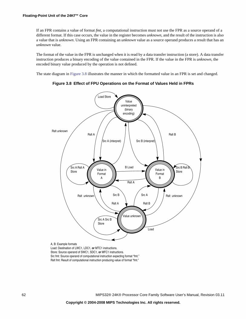
Floating-Point Unit of the 24Kf™ Core
62 MIPS32® 24K® Processor Core Family Software User’s Manual, Revision 03.11
Copyright © 2004-2008 MIPS Technologies Inc. All rights reserved.
If an FPR contains a value of format fmt, a computational instruction must not use the FPR as a source operand of adifferent format. If this case occurs, the value in the register becomes unknown, and the result of the instruction is alsoa value that is unknown. Using an FPR containing an unknown value as a source operand produces a result that has anunknown value.
The format of the value in the FPR is unchanged when it is read by a data transfer instruction (a store). A data transferinstruction produces a binary encoding of the value contained in the FPR. If the value in the FPR is unknown, theencoded binary value produced by the operation is not defined.
The state diagram in Figure 3.8 illustrates the manner in which the formatted value in an FPR is set and changed.
Figure 3.8 Effect of FPU Operations on the Format of Values Held in FPRs
A, B: Example formatsLoad: Destination of LWC1, LDC1, or MTC1 instructions.Store: Source operand of SWC1, SDC1, or MFC1 instructions.Src fmt: Source operand of computational instruction expecting format “fmt.”Rslt fmt: Result of computational instruction producing value of format “fmt.”
Load Store
Rslt unknownRslt A Rslt B
Src A (interpret) Src B (interpret)
B Load
Rslt A
Src B Src A
Rslt A Rslt B
Rslt unknown Rslt unknown
Src A Src BStore
Load
Src A Rslt AStore
Src B Rslt BStoreValue in
FormatA
Valueuninterpreted
(binaryencoding)
Value inFormat
B
Value unknown

3.4 Floating-Point General Registers
MIPS32® 24K® Processor Core Family Software User’s Manual, Revision 03.11 63
Copyright © 2004-2008 MIPS Technologies Inc. All rights reserved.
3.4.3 Binary Data Transfers (32-Bit and 64-Bit)
The data transfer instructions move words and doublewords between the FPU FPRs and the remainder of the system.The operations of the word and doubleword load and move-to instructions are shown in Figure 3.9 and Figure 3.10,respectively.
The store and move-from instructions operate in reverse, reading data from the location that the corresponding loador move-to instruction had written.
Figure 3.9 FPU Word Load and Move-to Operations
Figure 3.10 FPU Doubleword Load and Move-to Operations
Reg 0
Reg 1
63 0FR BIT = 1 FR BIT = 0
Reg 0
Reg 1
Reg 0
Reg 1
Initial value 1
Initial value 2
Undefined/Unused Data word (0)
Initial value 2
Undefined/Unused
Undefined/Unused
Data word (0)
Data word (4)
63 0
63 0
63 0
63 0
63 0
Reg 0
Reg 2
Reg 0
Reg 2
Reg 0
Reg 2
Undefined/Unused Data word (0)
Initial value 2
Data word (4) Data word (0)
Initial value 2
Initial value 1
Initial value 2
LWC1 f0, 0(r0) / MTC1 f0,r0
LWC1 f1, 4(r0) / MTC1 f1,r4
Reg 0
Reg 1
63 0
FR BIT = 1 FR BIT = 0
Initial value 1
Initial value 2
Data doubleword (0)
63 0
63 0
63 0
Reg 0
Reg 2
LDC1 f0, 0(r0)
LDC1 f1, 8(r0)
Reg 0
Reg 1
Reg 0
Reg 1
Initial value 1
Initial value 2
Reg 0
Reg 2 Initial value 2
Data doubleword (0)
Data doubleword (8)
63 0
(Illegal when FR BIT = 0)
Data doubleword (0)
Initial value 2
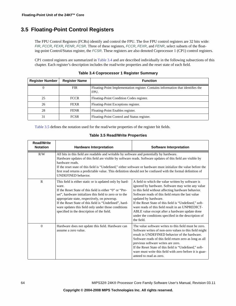
Floating-Point Unit of the 24Kf™ Core
64 MIPS32® 24K® Processor Core Family Software User’s Manual, Revision 03.11
Copyright © 2004-2008 MIPS Technologies Inc. All rights reserved.
3.5 Floating-Point Control Registers
The FPU Control Registers (FCRs) identify and control the FPU. The five FPU control registers are 32 bits wide:FIR, FCCR, FEXR, FENR, FCSR. Three of these registers, FCCR, FEXR, and FENR, select subsets of the float-ing-point Control/Status register, the FCSR. These registers are also denoted Coprocessor 1 (CP1) control registers.
CP1 control registers are summarized in Table 3.4 and are described individually in the following subsections of thischapter. Each register’s description includes the read/write properties and the reset state of each field.
Table 3.5 defines the notation used for the read/write properties of the register bit fields.
Table 3.4 Coprocessor 1 Register Summary
Register Number Register Name Function
0 FIR Floating-Point Implementation register. Contains information that identifies theFPU.
25 FCCR Floating-Point Condition Codes register.
26 FEXR Floating-Point Exceptions register.
28 FENR Floating-Point Enables register.
31 FCSR Floating-Point Control and Status register.
Table 3.5 Read/Write Properties
Read/WriteNotation Hardware Interpretation Software Interpretation
R/W All bits in this field are readable and writable by software and potentially by hardware.Hardware updates of this field are visible by software reads. Software updates of this field are visible byhardware reads.If the reset state of this field is “Undefined,” either software or hardware must initialize the value before thefirst read returns a predictable value. This definition should not be confused with the formal definition ofUNDEFINED behavior.
R This field is either static or is updated only by hard-ware.If the Reset State of this field is either “0” or “Pre-set”, hardware initializes this field to zero or to theappropriate state, respectively, on powerup.If the Reset State of this field is “Undefined”, hard-ware updates this field only under those conditionsspecified in the description of the field.
A field to which the value written by software isignored by hardware. Software may write any valueto this field without affecting hardware behavior.Software reads of this field return the last valueupdated by hardware.If the Reset State of this field is “Undefined,” soft-ware reads of this field result in an UNPREDICT-ABLE value except after a hardware update doneunder the conditions specified in the description ofthe field.
0 Hardware does not update this field. Hardware canassume a zero value.
The value software writes to this field must be zero.Software writes of non-zero values to this field mightresult in UNDEFINED behavior of the hardware.Software reads of this field return zero as long as allprevious software writes are zero.If the Reset State of this field is “Undefined,” soft-ware must write this field with zero before it is guar-anteed to read as zero.

3.5 Floating-Point Control Registers
MIPS32® 24K® Processor Core Family Software User’s Manual, Revision 03.11 65
Copyright © 2004-2008 MIPS Technologies Inc. All rights reserved.
3.5.1 Floating-Point Implementation Register (FIR, CP1 Control Register 0)
The Floating-Point Implementation Register (FIR) is a 32-bit read-only register that contains information identifyingthe capabilities of the FPU, the Floating-Point processor identification, and the revision level of the FPU. Figure 3.11shows the format of the FIR; Table 3.6 describes the FIR bit fields.
Figure 3.11 FIR Format31 25 24 23 22 21 20 19 18 17 16 15 8 7 0
0 FC 0 F64 L W 3D PS D S ProcessorID Revision
Table 3.6 FIR Bit Field Descriptions
Fields
DescriptionRead /Write Reset StateName Bits
FC 24 Indicates that full convert ranges are implemented:0: Full convert ranges not implemented1: Full convert ranges implementedThis bit is always 1 to indicate that full convert ranges areimplemented. This means that all numbers can be con-verted to another type by the FPU (If FS bit in FCSR is notset Unimplemented Operation exception can still happenon denormal operands though).
R 1
F64 22 Indicates that this is a 64-bit FPU:0: Not a 64-bit FPU1: A 64-bit FPU.This bit is always 1 to indicate that this is a 64-bit FPU.
R 1
L 21 Indicates that the long fixed point (L) data type andinstructions are implemented:0: Long type not implemented1: Long implementedThis bit is always 1 to indicate that long fixed point datatypes are implemented.
R 1
W 20 Indicates that the word fixed point (W) data type andinstructions are implemented:0: Word type not implemented1: Word implementedThis bit is always 1 to indicate that word fixed point datatypes are implemented.
R 1
3D 19 Indicates that the MIPS-3D ASE is implemented:0: MIPS-3D not implemented1: MIPS-3D implementedThis bit is always 0 to indicate that MIPS-3D is not imple-mented.
R 0
PS 18 Indicates that the paired-single (PS) floating-point datatype and instructions are implemented:0: PS floating-point not implemented1: PS floating-point implementedThis bit is always 0 to indicate that paired-single float-ing-point data types are not implemented.
R 0

Floating-Point Unit of the 24Kf™ Core
66 MIPS32® 24K® Processor Core Family Software User’s Manual, Revision 03.11
Copyright © 2004-2008 MIPS Technologies Inc. All rights reserved.
3.5.2 Floating-Point Condition Codes Register (FCCR, CP1 Control Register 25)
The Floating-Point Condition Codes Register (FCCR) is an alternative way to read and write the floating-point condi-tion code values that also appear in the FCSR. Unlike the FCSR, all eight FCC bits are contiguous in the FCCR.Figure 3.12 shows the format of the FCCR; Table 3.7 describes the FCCR bit fields.
Figure 3.12 FCCR Format
D 17 Indicates that the double-precision (D) floating-point datatype and instructions are implemented:0: D floating-point not implemented1: D floating-point implementedThis bit is always 1 to indicate that double-precision float-ing-point data types are implemented.
R 1
S 16 Indicates that the single-precision (S) floating-point datatype and instructions are implemented:0: S floating-point not implemented1: S floating-point implementedThis bit is always 1 to indicate that single-precision float-ing-point data types are implemented.
R 1
Processor ID 15:8 Identifies the floating-point processor. This value matchesthe corresponding field of the CP0 PRId register.
R 0x93
Revision 7:0 Specifies the revision number of the FPU. This fieldallows software to distinguish between one revision andanother of the same floating-point processor type. Thisvalue matches the corresponding field of the CP0 PRIdregister.
R Hardwired
0 31:25, 23 These bits must be written as zeros; they return zeros onreads.
0 0
31 8 7 0
0 FCC
Table 3.7 FCCR Bit Field Descriptions
Fields
DescriptionRead /Write Reset StateName Bits
FCC 7:0 Floating-point condition code. Refer to the description ofthis field in Section 3.5.5 “Floating-Point Control andStatus Register (FCSR, CP1 Control Register 31)”.
R/W Undefined
0 31:8 These bits must be written as zeros; they return zeros onreads.
0 0
Table 3.6 FIR Bit Field Descriptions (Continued)
Fields
DescriptionRead /Write Reset StateName Bits
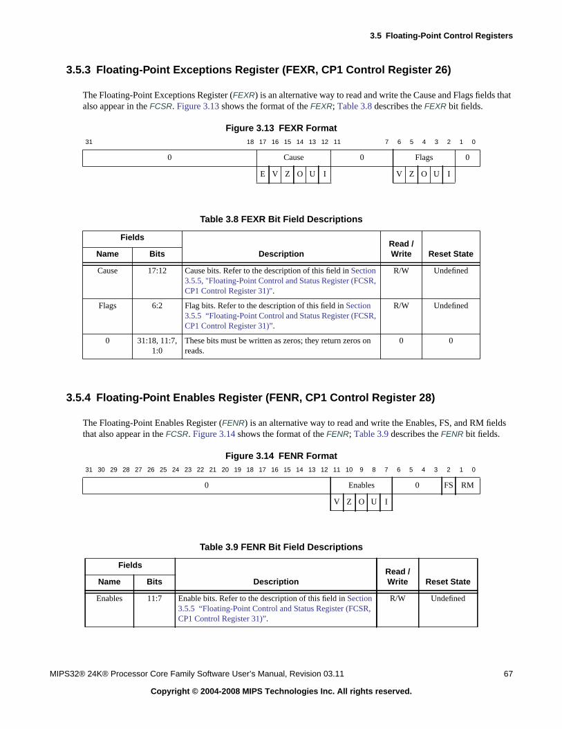
3.5 Floating-Point Control Registers
MIPS32® 24K® Processor Core Family Software User’s Manual, Revision 03.11 67
Copyright © 2004-2008 MIPS Technologies Inc. All rights reserved.
3.5.3 Floating-Point Exceptions Register (FEXR, CP1 Control Register 26)
The Floating-Point Exceptions Register (FEXR) is an alternative way to read and write the Cause and Flags fields thatalso appear in the FCSR. Figure 3.13 shows the format of the FEXR; Table 3.8 describes the FEXR bit fields.
Figure 3.13 FEXR Format
3.5.4 Floating-Point Enables Register (FENR, CP1 Control Register 28)
The Floating-Point Enables Register (FENR) is an alternative way to read and write the Enables, FS, and RM fieldsthat also appear in the FCSR. Figure 3.14 shows the format of the FENR; Table 3.9 describes the FENR bit fields.
Figure 3.14 FENR Format
31 18 17 16 15 14 13 12 11 7 6 5 4 3 2 1 0
0 Cause 0 Flags 0
E V Z O U I V Z O U I
Table 3.8 FEXR Bit Field Descriptions
Fields
DescriptionRead /Write Reset StateName Bits
Cause 17:12 Cause bits. Refer to the description of this field in Section3.5.5, "Floating-Point Control and Status Register (FCSR,CP1 Control Register 31)".
R/W Undefined
Flags 6:2 Flag bits. Refer to the description of this field in Section3.5.5 “Floating-Point Control and Status Register (FCSR,CP1 Control Register 31)”.
R/W Undefined
0 31:18, 11:7,1:0
These bits must be written as zeros; they return zeros onreads.
0 0
31 30 29 28 27 26 25 24 23 22 21 20 19 18 17 16 15 14 13 12 11 10 9 8 7 6 5 4 3 2 1 0
0 Enables 0 FS RM
V Z O U I
Table 3.9 FENR Bit Field Descriptions
Fields
DescriptionRead /Write Reset StateName Bits
Enables 11:7 Enable bits. Refer to the description of this field in Section3.5.5 “Floating-Point Control and Status Register (FCSR,CP1 Control Register 31)”.
R/W Undefined

Floating-Point Unit of the 24Kf™ Core
68 MIPS32® 24K® Processor Core Family Software User’s Manual, Revision 03.11
Copyright © 2004-2008 MIPS Technologies Inc. All rights reserved.
3.5.5 Floating-Point Control and Status Register (FCSR, CP1 Control Register 31)
The 32-bit Floating-Point Control and Status Register (FCSR) controls the operation of the FPU and shows the fol-lowing status information:
• selects the default rounding mode for FPU arithmetic operations
• selectively enables traps of FPU exception conditions
• controls some denormalized number handling options
• reports any IEEE exceptions that arose during the most recently executed instruction
• reports any IEEE exceptions that cumulatively arose in completed instructions
• indicates the condition code result of FP compare instructions
Access to the FCSR is not privileged; it can be read or written by any program that has access to the FPU (via thecoprocessor enables in the Status register). Figure 3.15 shows the format of the FCSR; Table 3.10 describes the FCSRbit fields.
Figure 3.15 FCSR Format
FS 2 Flush to Zero bit. Refer to the description of this field inSection 3.5.5, "Floating-Point Control and Status Register(FCSR, CP1 Control Register 31)".
R/W Undefined
RM 1:0 Rounding mode. Refer to the description of this field inSection 3.5.5, "Floating-Point Control and Status Register(FCSR, CP1 Control Register 31)".
R/W Undefined
0 31:12, 6:3 These bits must be written as zeros; they return zeros onreads.
0 0
31 25 24 23 22 21 20 18 17 12 11 7 6 2 1 0
FCC FS FCC FO FN 0 Cause Enables Flags RM
7 6 5 4 3 2 1 0 E V Z O U I V Z O U I V Z O U I
Table 3.9 FENR Bit Field Descriptions (Continued)
Fields
DescriptionRead /Write Reset StateName Bits

3.5 Floating-Point Control Registers
MIPS32® 24K® Processor Core Family Software User’s Manual, Revision 03.11 69
Copyright © 2004-2008 MIPS Technologies Inc. All rights reserved.
Table 3.10 FCSR Bit Field Descriptions
Fields
DescriptionRead /Write Reset StateName Bit
FCC 31:25, 23 Floating-point condition codes. These bits record theresult of floating-point compares and are tested for float-ing-point conditional branches and conditional moves.The FCC bit to use is specified in the compare, branch, orconditional move instruction. For backward compatibilitywith previous MIPS ISAs, the FCC bits are separated intotwo non-contiguous fields.
R/W Undefined
FS 24 Flush to Zero (FS). Refer to Section 3.5.6 “Operation ofthe FS/FO/FN Bits” for more details on this bit.
R/W Undefined
FO 22 Flush Override (FO). Refer to Section 3.5.6 “Operation ofthe FS/FO/FN Bits” for more details on this bit.
R/W Undefined
FN 21 Flush to Nearest (FN). Refer to Section 3.5.6 “Operationof the FS/FO/FN Bits” for more details on this bit.
R/W Undefined
Cause 17:12 Cause bits. These bits indicate the exception conditionsthat arise during execution of an FPU arithmetic instruc-tion. A bit is set to 1 when the corresponding exceptioncondition arises during the execution of an instruction;otherwise, it is cleared to 0. By reading the registers, theexception condition caused by the preceding FPU arith-metic instruction can be determined.Refer to Table 3.11 for the meaning of each cause bit.
R/W Undefined
Enables 11:7 Enable bits. These bits control whether or not a trap istaken when an IEEE exception condition occurs for any ofthe five conditions. The trap occurs when both an enablebit and its corresponding cause bit are set either during anFPU arithmetic operation or by moving a value to theFCSR or one of its alternative representations. Note thatCause bit E (CauseE) has no corresponding enable bit; theMIPS architecture defines non-IEEE UnimplementedOperation exceptions as always enabled.Refer to Table 3.11 for the meaning of each enable bit.
R/W Undefined
Flags 6:2 Flag bits. This field shows any exception conditions thathave occurred for completed instructions since the flagwas last reset by software.When an FPU arithmetic operation raises an IEEE excep-tion condition that does not result in a Floating-PointException (the enable bit was off), the correspondingbit(s) in the Flags field are set, while the others remainunchanged. Arithmetic operations that result in a Float-ing-Point Exception (the enable bit was on) do not updatethe Flags field.Hardware never resets this field; software must explicitlyreset this field.Refer to Table 3.11 for the meaning of each flag bit.
R/W Undefined

Floating-Point Unit of the 24Kf™ Core
70 MIPS32® 24K® Processor Core Family Software User’s Manual, Revision 03.11
Copyright © 2004-2008 MIPS Technologies Inc. All rights reserved.
3.5.6 Operation of the FS/FO/FN Bits
The FS, FO, and FN bits in the CP1 FCSR register control handling of denormalized operands and tiny results (i.e.
nonzero result between ±2E_min), whereby the FPU can handle these cases right away instead of relying on the muchslower software handler. The trade-off is a loss of IEEE compliance and accuracy (except for use of the FO bit),because a minimal normalized or zero result is provided by the FPU instead of the more accurate denormalized resultthat a software handler would give. The benefit is a significantly improved performance and precision.
RM 1:0 Rounding mode. This field indicates the rounding modeused for most floating-point operations (some operationsuse a specific rounding mode).Refer to Table 3.12 for the encoding of this field.
R/W Undefined
0 20:18 These bits must be written as zeros; they return zeros onreads.
0 0
Table 3.11 Cause, Enables, and Flags Definitions
Bit Name Bit Meaning
E Unimplemented Operation (this bit exists only in the Cause field).
V Invalid Operations
Z Divide by Zero
O Overflow
U Underflow
I Inexact
Table 3.12 Rounding Mode Definitions
RM FieldEncoding Meaning
0 RN - Round to NearestRounds the result to the nearest representable value. When two representable values are equallynear, the result is rounded to the value whose least significant bit is zero (even).
1 RZ - Round Toward ZeroRounds the result to the value closest to but not greater in magnitude than the result.
2 RP - Round Towards Plus InfinityRounds the result to the value closest to but not less than the result.
3 RM - Round Towards Minus InfinityRounds the result to the value closest to but not greater than the result.
Table 3.10 FCSR Bit Field Descriptions (Continued)
Fields
DescriptionRead /Write Reset StateName Bit

3.5 Floating-Point Control Registers
MIPS32® 24K® Processor Core Family Software User’s Manual, Revision 03.11 71
Copyright © 2004-2008 MIPS Technologies Inc. All rights reserved.
Use of the FS, FO, and FN bits affects handling of denormalized floating-point numbers and tiny results for theinstructions listed below:
Instructions not listed above do not cause Unimplemented Operation exceptions on denormalized numbers in oper-ands or results.
Figure 3.16 depicts how the FS, FO, and FN bits control handling of denormalized numbers. For instructions that arenot multiply or add types (such as DIV), only the FS and FN bits apply.
Figure 3.16 FS/FO/FN Bits Influence on Multiply and Addition Results
3.5.6.1 Flush To Zero Bit
When the Flush To Zero (FS) bit is set, denormal input operands are flushed to zero. Tiny results are flushed to eitherzero or the applied format’s smallest normalized number (MinNorm) depending on the rounding mode settings. Table3.13 lists the flushing behavior for tiny results..
The flushing of results is based on an intermediate result computed by rounding the mantissa using an unboundedexponent range; that is, tiny numbers are not normalized into the supported exponent range by shifting in leadingzeros prior to rounding.
Handling of denormalized operand values and tiny results depends on the FS bit setting as shown in Table 3.14.
FS and FN bit: ADD, CEIL, CVT, DIV, FLOOR, MADD, MSUB, MUL, NMADD, NMSUB, RECIP, ROUND,
RSQRT, SQRT, TRUNC, SUB, ABS, C.cond, and NEG1
1. For ABS, C.cond, and NEG, denormal input operands or tiny results doe not result in Unimplemented exceptions whenFS = 0. Flushing to zero nonetheless is implemented when FS = 1 such that these operations return the same result as anequivalent sequence of arithmetic FPU operations.
FO bit: MADD, MSUB, NMADD, and NMSUB
Table 3.13 Zero Flushing for Tiny Results
Rounding Mode Negative Tiny Result Positive Tiny Result
RN (RM=0) -0 +0
RZ(RM=1) -0 +0
RP (RM=2) -0 +MinNorm
RM (RM=3) -MinNorm +0
Table 3.14 Handling of Denormalized Operand Values and Tiny Results Based on FS Bit Setting
FS Bit Handling of Denormalized Operand Values
0 An Unimplemented Operation exception is taken.
Operand valuesFS applies
AdditionMultiply
Intermediate Multiply-Add resultFS/FO applies
Final resultFS/FN applies

Floating-Point Unit of the 24Kf™ Core
72 MIPS32® 24K® Processor Core Family Software User’s Manual, Revision 03.11
Copyright © 2004-2008 MIPS Technologies Inc. All rights reserved.
3.5.6.2 Flush Override Bit
When the Flush Override (FO) bit is set, a tiny intermediate result of any multiply-add type instruction is not flushedaccording to the FS bit. The intermediate result is maintained in an internal normalized format to improve accuracy.FO only applies to the intermediate result of a multiply-add type instruction.
Handling of tiny intermediate results depends on the FO and FS bits as shown in Table 3.15.
3.5.6.3 Flush to Nearest
When the Flush to Nearest (FN) bit is set and the rounding mode is Round to Nearest (RN), a tiny final result isflushed to zero or MinNorm. If a tiny number is strictly below MinNorm/2, the result is flushed to zero; otherwise, itis flushed to MinNorm (see Figure 3.17). The flushed result has the same sign as the result prior to flushing. Note thatthe FN bit takes precedence over the FS bit.
Figure 3.17 Flushing to Nearest when Rounding Mode is Round to Nearest
For all rounding modes other than Round to Nearest (RN), setting the FN bit causes final results to be flushed to zeroor MinNorm as if the FS bit was set.
Handling of tiny final results depends on the FN and FS bits as shown in Table 3.16.
1 Instead of causing an Unimplemented Operation exception, operands are flushed to zero, and tinyresults are forced to zero or MinNorm.
Table 3.15 Handling of Tiny Intermediate Result Based on the FO and FS Bit Settings
FO Bit FS Bit Handling of Tiny Result Values
0 0 An Unimplemented Operation exception is taken.
0 1 The intermediate result is forced to the value that would have been delivered for anuntrapped underflow (see Table 3.32) instead of causing an Unimplemented Operationexception.
1 Don’t care The intermediate result is kept in an internal format, which can be perceived as havingthe usual mantissa precision but with unlimited exponent precision and without forcingto a specific value or taking an exception.
Table 3.16 Handling of Tiny Final Result Based on FN and FS Bit Settings
FN Bit FS Bit Handling of Tiny Result Values
0 0 An Unimplemented Operation exception is taken.
Table 3.14 Handling of Denormalized Operand Values and Tiny Results Based on FS Bit Setting
FS Bit Handling of Denormalized Operand Values
MinNorm/2-MinNorm/2
-MinNorm MinNorm0

3.5 Floating-Point Control Registers
MIPS32® 24K® Processor Core Family Software User’s Manual, Revision 03.11 73
Copyright © 2004-2008 MIPS Technologies Inc. All rights reserved.
3.5.6.4 Recommended FS/FO/FN Settings
Table 3.17 summarizes the recommended FS/FO/FN settings.
3.5.7 FCSR Cause Bit Update Flow
3.5.7.1 Exceptions Triggered by CTC1
Regardless of the targeted control register, the CTC1 instruction causes the Enables and Cause fields of the FCSR tobe inspected in order to determine if an exception is to be thrown.
3.5.7.2 Generic Flow
Computations are performed in two steps:
1. Compute rounded mantissa with unbound exponent range.
2. Flush to default result if the result from Step #1 above is overflow or tiny (no flushing happens on denorms forinstructions supporting denorm results, such as MOV).
The Cause field is updated after each of these two steps. Any enabled exceptions detected in these two steps cause atrap, and no further updates to the Cause field are done by subsequent steps.
Step #1 can set cause bits I, U, O, Z, V, and E. E has priority over V; V has priority over Z; and Z has priority over Uand O. Thus when E, V, or Z is set in Step #1, no other cause bits can be set. However, note that I and V both can beset if a denormal operand was flushed (FS = 1). I, U, and O can be set alone or in pairs (IU or IO). U and O never canbe set simultaneously in Step #1. U and O are set if the computed unbounded exponent is outside the exponent rangesupported by the normalized IEEE format.
Step #2 can set I if a default result is generated.
0 1 Final result is forced to the value that would have been delivered for an untrapped under-flow (see Table 3.32) rather than causing an Unimplemented Operation exception.
1 Don’t care Final result is rounded to either zero or 2E_min (MinNorm), whichever is closest when inRound to Nearest (RN) rounding mode. For other rounding modes, a final result is givenas if FS was set to 1.
Table 3.17 Recommended FS/FO/FN Settings
FS Bit FO Bit FN Bit Remarks
0 0 0 IEEE-compliant mode. Low performance on denormal operands and tiny results.
1 0 0 Regular embedded applications. High performance on denormal operands andtiny results.
1 1 1 Highest accuracy and performance configuration.1
1. Note that in this mode, MADD might return a different result other than the equivalent MUL and ADD operationsequence.
Table 3.16 Handling of Tiny Final Result Based on FN and FS Bit Settings (Continued)
FN Bit FS Bit Handling of Tiny Result Values
Floating-Point Unit of the 24Kf™ Core
74 MIPS32® 24K® Processor Core Family Software User’s Manual, Revision 03.11
Copyright © 2004-2008 MIPS Technologies Inc. All rights reserved.
3.5.7.3 Multiply-Add Flow
For multiply-add type instructions, the computation is extended with two more steps:
1. Compute rounded mantissa with unbound exponent range for the multiply.
2. Flush to default result if the result from Step #1 is overflow or tiny (no flushing happens on tiny results ifFO = 1).
3. Compute rounded mantissa with unbounded exponent range for the add.
4. Flush to default result if the result from Step #3 is overflow or tiny.
The Cause field is updated after each of these four steps. Any enabled exceptions detected in these four steps cause atrap, and no further updates to the Cause field are done by subsequent steps.
Step #1 and Step #3 can set a cause bit as described for Step #1 in Section 3.5.7.2 “Generic Flow”.
Step #2 and Step #4 can set I if a default result is generated.
Although U and O can never both be set in Step #1 or Step #3, both U and O might be set after the multiply-add hasexecuted in Step #3 because U might be set in Step #1 and O might be set in Step #3.
3.5.7.4 Cause Update Flow for Input Operands
Denormal input operands to Step #1 or Step #3 always set Cause bit I when FS = 1. For example, SNaN+DeNorm setI (and V) provided that Step #3 was reached (in case of a multiply-add type instruction).
Conditions directly related to the input operand (for example, I/E set due to DeNorm, V set due to SNaN and QNaNpropagation) are detected in the step where the operand is logically used. For example, for multiply-add type instruc-tions, exceptional conditions caused by the input operand fr are detected in Step #3.
3.5.7.5 Cause Update Flow for Unimplemented Operations
Note that Cause bit E is special; it clears any Cause updates done in previous steps. For example, if Step #3 caused Eto be set, any I, U, or O Cause update done in Step #1 or Step #2 is cleared. Only E is set in the Cause field when anUnimplemented Operation trap is taken.
3.6 Instruction Overview
The functional groups into which the FPU instructions are divided are described in the following subsections:
• Section 3.6.1 “Data Transfer Instructions”
• Section 3.6.2 “Arithmetic Instructions”
• Section 3.6.3 “Conversion Instructions”
• Section 3.6.4 “Formatted Operand-Value Move Instructions”
• Section 3.6.5 “Conditional Branch Instructions”

3.6 Instruction Overview
MIPS32® 24K® Processor Core Family Software User’s Manual, Revision 03.11 75
Copyright © 2004-2008 MIPS Technologies Inc. All rights reserved.
• Section 3.6.6 “Miscellaneous Instructions”
The instructions are described in detail in Chapter 12, “24K® Processor Core Instructions” on page 303, includingdescriptions of supported formats (fmt).
3.6.1 Data Transfer Instructions
The FPU has two separate register sets: coprocessor general registers (FPRs) and coprocessor control registers(FCRs). The FPU has a load/store architecture; all computations are done on data held in coprocessor general regis-ters. The control registers are used to control FPU operation. Data is transferred between registers and the rest of thesystem with dedicated load, store, and move instructions. The transferred data is treated as unformatted binary data;no format conversions are performed, and therefore no IEEE floating-point exceptions can occur.
Table 3.18 lists the supported transfer operations.
3.6.1.1 Data Alignment in Loads, Stores, and Moves
All coprocessor loads and stores operate on naturally aligned data items. An attempt to load or store to an address thatis not naturally aligned for the data item causes an Address Error exception. Regardless of byte ordering (the endian-ness), the address of a word or doubleword is the smallest byte address in the object. For a big-endian machine, this isthe most-significant byte; for a little-endian machine, this is the least-significant byte.
3.6.1.2 Addressing Used in Data Transfer Instructions
The FPU has loads and stores using the same register+offset addressing as that used by the CPU. Moreover, for theFPU only, there are load and store instructions using register+register addressing.
Tables 3.19 through 3.20 list the FPU data transfer instructions.
Table 3.18 FPU Data Transfer Instructions
Transfer Direction Data Transferred
FPU general register ↔ Memory Word/doubleword load/store
FPU general register ↔ CPU general register Word move
FPU control register ↔ CPU general register Word move
Table 3.19 FPU Loads and Stores Using Register+Offset Address Mode
Mnemonic Instruction
LDC1 Load Doubleword to Floating Point
LWC1 Load Word to Floating Point
SDC1 Store Doubleword to Floating Point
SWC1 Store Word to Floating Point

Floating-Point Unit of the 24Kf™ Core
76 MIPS32® 24K® Processor Core Family Software User’s Manual, Revision 03.11
Copyright © 2004-2008 MIPS Technologies Inc. All rights reserved.
3.6.2 Arithmetic Instructions
Arithmetic instructions operate on formatted data values. The results of most floating-point arithmetic operationsmeet IEEE Standard 754 for accuracy—a result is identical to an infinite-precision result that has been rounded to thespecified format using the current rounding mode. The rounded result differs from the exact result by less than oneUnit in the Least-significant Place (ULP).
In general, the arithmetic instructions take an Umimplemented Operation exception for denormalized numbers,except for the ABS, C, and NEG instructions, which can handle denormalized numbers. The FS, FO, and FN bits inthe CP1 FCSR register can override this behavior as described in Section 3.5.6 “Operation of the FS/FO/FN Bits”.
Table 3.21 lists the FPU IEEE compliant arithmetic operations.
The two low latency operations, Reciprocal Approximation (RECIP) and Reciprocal Square Root Approximation(RSQRT), might be less accurate than the IEEE specification:
• The result of RECIP differs from the exact reciprocal by no more than one ULP.
• The result of RSQRT differs from the exact reciprocal square root by no more than two ULPs.
Table 3.22 lists the FPU-approximate arithmetic operations.
Table 3.20 FPU Move To and From Instructions
Mnemonic Instruction
CFC1 Move Control Word From Floating Point
CTC1 Move Control Word To Floating Point
MFC1 Move Word From Floating Point
MTC1 Move Word To Floating Point
Table 3.21 FPU IEEE Arithmetic Operations
Mnemonic Instruction
ABS.fmt Floating-Point Absolute Value
ADD.fmt Floating-Point Add
C.cond.fmt Floating-Point Compare
DIV.fmt Floating-Point Divide
MUL.fmt Floating-Point Multiply
NEG.fmt Floating-Point Negate
SQRT.fmt Floating-Point Square Root
SUB.fmt Floating-Point Subtract
Table 3.22 FPU-Approximate Arithmetic Operations
Mnemonic Instruction
RECIP.fmt Floating-Point Reciprocal Approximation

3.6 Instruction Overview
MIPS32® 24K® Processor Core Family Software User’s Manual, Revision 03.11 77
Copyright © 2004-2008 MIPS Technologies Inc. All rights reserved.
Four compound-operation instructions perform variations of multiply-accumulate operations; that is, multiply twooperands, accumulate the result to a third operand, and produce a result. These instructions are listed in Table 3.23.The product is rounded according to the current rounding mode prior to the accumulation. This model meets the IEEEaccuracy specification; the result is numerically identical to an equivalent computation using multiply, add, subtract,or negate instructions.
3.6.3 Conversion Instructions
These instructions perform conversions between floating-point and fixed-point data types. Each instruction convertsvalues from a number of operand formats to a particular result format. Some conversion instructions use the roundingmode specified in the Floating Control/Status register (FCSR), while others specify the rounding mode directly.
In general, the conversion instructions only take an Umimplemented Operation exception for denormalized numbers.The FS and FN bits in the CP1 FCSR register can override this behavior as described in Section 3.5.6 “Operation ofthe FS/FO/FN Bits”.
Table 3.24 and Table 3.25 list the FPU conversion instructions according to their rounding mode.
RSQRT.fmt Floating-Point Reciprocal Square Root Approximation
Table 3.23 FPU Multiply-Accumulate Arithmetic Operations
Mnemonic Instruction
MADD.fmt Floating-Point Multiply Add
MSUB.fmt Floating-Point Multiply Subtract
NMADD.fmt Floating-Point Negative Multiply Add
NMSUB.fmt Floating-Point Negative Multiply Subtract
Table 3.24 FPU Conversion Operations Using the FCSR Rounding Mode
Mnemonic Instruction
CVT.D.fmt Floating-Point Convert to Double Floating Point
CVT.L.fmt Floating-Point Convert to Long Fixed Point
CVT.S.fmt Floating-Point Convert to Single Floating Point
CVT.W.fmt Floating-Point Convert to Word Fixed Point
Table 3.25 FPU Conversion Operations Using a Directed Rounding Mode
Mnemonic Instruction
CEIL.L.fmt Floating-Point Ceiling to Long Fixed Point
CEIL.W.fmt Floating-Point Ceiling to Word Fixed Point
FLOOR.L.fmt Floating-Point Floor to Long Fixed Point
FLOOR.W.fmt Floating-Point Floor to Word Fixed Point
ROUND.L.fmt Floating-Point Round to Long Fixed Point
Table 3.22 FPU-Approximate Arithmetic Operations (Continued)
Mnemonic Instruction

Floating-Point Unit of the 24Kf™ Core
78 MIPS32® 24K® Processor Core Family Software User’s Manual, Revision 03.11
Copyright © 2004-2008 MIPS Technologies Inc. All rights reserved.
3.6.4 Formatted Operand-Value Move Instructions
These instructions move formatted operand values among FPU general registers. A particular operand type must bemoved by the instruction that handles that type. There are three kinds of move instructions:
• Unconditional move
• Conditional move that tests an FPU true/false condition code
• Conditional move that tests a CPU general-purpose register against zero
Conditional move instructions operate in a way that might be unexpected. They always force the value in the destina-tion register to become a value of the format specified in the instruction. If the destination register does not contain anoperand of the specified format before the conditional move is executed, the contents become undefined. (For moreinformation, see the individual descriptions of the conditional move instructions in the MIPS32 Architecture Refer-ence Manual, Volume II [2].)
Table 3.26 through Table 3.28 list the formatted operand-value move instructions.
ROUND.W.fmt Floating-Point Round to Word Fixed Point
TRUNC.L.fmt Floating-Point Truncate to Long Fixed Point
TRUNC.W.fmt Floating-Point Truncate to Word Fixed Point
Table 3.26 FPU Formatted Operand Move Instruction
Mnemonic Instruction
MOV.fmt Floating-Point Move
Table 3.27 FPU Conditional Move on True/False Instructions
Mnemonic Instruction
MOVF.fmt Floating-Point Move Conditional on FP False
MOVT.fmt Floating-Point Move Conditional on FP True
Table 3.28 FPU Conditional Move on Zero/Non-Zero Instructions
Mnemonic Instruction
MOVN.fmt Floating-Point Move Conditional on Nonzero
MOVZ.fmt Floating-Point Move Conditional on Zero
Table 3.25 FPU Conversion Operations Using a Directed Rounding Mode (Continued)
Mnemonic Instruction

3.6 Instruction Overview
MIPS32® 24K® Processor Core Family Software User’s Manual, Revision 03.11 79
Copyright © 2004-2008 MIPS Technologies Inc. All rights reserved.
3.6.5 Conditional Branch Instructions
The FPU has PC-relative conditional branch instructions that test condition codes set by FPU compare instructions(C.cond.fmt).
All branches have an architectural delay of one instruction. When a branch is taken, the instruction immediately fol-lowing the branch instruction is said to be in the branch delay slot; it is executed before the branch to the targetinstruction takes place. Conditional branches come in two versions, depending upon how they handle an instructionin the delay slot when the branch is not taken and execution falls through:
• Branch instructions execute the instruction in the delay slot.
• Branch likely instructions do not execute the instruction in the delay slot if the branch is not taken (they are saidto nullify the instruction in the delay slot).
Although the Branch Likely instructions are included, software is strongly encouraged to avoid the use ofthe Branch Likely instructions, as they will be removed from a future revision of the MIPS Architecture.
The MIPS64 architecture defines eight condition codes for use in compare and branch instructions. For backwardcompatibility with previous revisions of the ISA, condition code bit 0 and condition code bits 1 through 7 are in dis-continuous fields in the FCSR.
Table 3.29 lists the conditional branch (branch and branch likely) FPU instructions; Table 3.30 lists the deprecatedconditional branch likely instructions.
3.6.6 Miscellaneous Instructions
The MIPS32 architecture defines various miscellaneous instructions that conditionally move one CPU general regis-ter to another, based on an FPU condition code.
Table 3.31 lists these conditional move instructions.
Table 3.29 FPU Conditional Branch Instructions
Mnemonic Instruction
BC1F Branch on FP False
BC1T Branch on FP True
Table 3.30 Deprecated FPU Conditional Branch Likely Instructions
Mnemonic Instruction
BC1FL Branch on FP False Likely
BC1TL Branch on FP True Likely
Table 3.31 CPU Conditional Move on FPU True/False Instructions
Mnemonic Instruction
MOVN Move Conditional on FP False
MOVZ Move Conditional on FP True

Floating-Point Unit of the 24Kf™ Core
80 MIPS32® 24K® Processor Core Family Software User’s Manual, Revision 03.11
Copyright © 2004-2008 MIPS Technologies Inc. All rights reserved.
3.7 Exceptions
FPU exceptions are implemented in the MIPS FPU architecture with the Cause, Enables, and Flags fields of theFCSR. The flag bits implement IEEE exception status flags, and the cause and enable bits control exception trapping.Each field has a bit for each of the five IEEE exception conditions. The Cause field has an additional exception bit,Unimplemented Operation, used to trap for software emulation assistance. If an exception type is enabled through theEnables field of the FCSR, then the FPU is operating in precise exception mode for this type of exception.
3.7.1 Precise Exception Mode
In precise exception mode, a trap occurs before the instruction that causes the trap or any following instruction cancomplete and write its results. If desired, the software trap handler can resume execution of the interrupted instructionstream after handling the exception.
The Cause field reports per-bit instruction exception conditions. The cause bits are written during each floating-pointarithmetic operation to show any exception conditions that arise during the operation. A cause bit is set to 1 if its cor-responding exception condition arises; otherwise, it is cleared to 0.
A floating-point trap is generated any time both a cause bit and its corresponding enable bit are set. This case occurseither during the execution of a floating-point operation or when moving a value into the FCSR. There is no enablebit for Unimplemented Operations; this exception always generates a trap.
In a trap handler, exception conditions that arise during any trapped floating-point operations are reported in theCause field. Before returning from a floating-point interrupt or exception, or before setting cause bits with a move tothe FCSR, software first must clear the enabled cause bits by executing a move to the FCSR to prevent the trap frombeing erroneously retaken.
If a floating-point operation sets only non-enabled cause bits, no trap occurs and the default result defined by IEEEStandard 754 is stored (see Table 3.32). When a floating-point operation does not trap, the program can monitor theexception conditions by reading the Cause field.
The Flags field is a cumulative report of IEEE exception conditions that arise as instructions complete; instructionsthat trap do not update the flag bits. The flag bits are set to 1 if the corresponding IEEE exception is raised, otherwisethe bits are unchanged. There is no flag bit for the MIPS Unimplemented Operation exception. The flag bits are nevercleared as a side effect of floating-point operations, but they can be set or cleared by moving a new value into theFCSR.
3.7.2 Exception Conditions
The subsections below describe the following five exception conditions defined by IEEE Standard 754:
• Section 3.7.2.1 “Invalid Operation Exception”
• Section 3.7.2.2 “Division By Zero Exception”
• Section 3.7.2.3 “Underflow Exception”
• Section 3.7.2.4 “Overflow Exception”
• Section 3.7.2.5 “Inexact Exception”
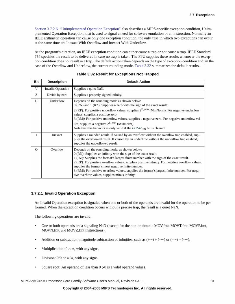
3.7 Exceptions
MIPS32® 24K® Processor Core Family Software User’s Manual, Revision 03.11 81
Copyright © 2004-2008 MIPS Technologies Inc. All rights reserved.
Section 3.7.2.6 “Unimplemented Operation Exception” also describes a MIPS-specific exception condition, Unim-plemented Operation Exception, that is used to signal a need for software emulation of an instruction. Normally anIEEE arithmetic operation can cause only one exception condition; the only case in which two exceptions can occurat the same time are Inexact With Overflow and Inexact With Underflow.
At the program’s direction, an IEEE exception condition can either cause a trap or not cause a trap. IEEE Standard754 specifies the result to be delivered in case no trap is taken. The FPU supplies these results whenever the excep-tion condition does not result in a trap. The default action taken depends on the type of exception condition and, in thecase of the Overflow and Underflow, the current rounding mode. Table 3.32 summarizes the default results.
3.7.2.1 Invalid Operation Exception
An Invalid Operation exception is signaled when one or both of the operands are invalid for the operation to be per-formed. When the exception condition occurs without a precise trap, the result is a quiet NaN.
The following operations are invalid:
• One or both operands are a signaling NaN (except for the non-arithmetic MOV.fmt, MOVT.fmt, MOVF.fmt,MOVN.fmt, and MOVZ.fmt instructions).
• Addition or subtraction: magnitude subtraction of infinities, such as (+∞) + (−∞) or (−∞) − (−∞).
• Multiplication: 0 × ∞, with any signs.
• Division: 0/0 or ∞/∞, with any signs.
• Square root: An operand of less than 0 (-0 is a valid operand value).
Table 3.32 Result for Exceptions Not Trapped
Bit Description Default Action
V Invalid Operation Supplies a quiet NaN.
Z Divide by zero Supplies a properly signed infinity.
U Underflow Depends on the rounding mode as shown below:0 (RN) and 1 (RZ): Supplies a zero with the sign of the exact result.
2 (RP): For positive underflow values, supplies 2E_min (MinNorm). For negative underflowvalues, supplies a positive zero.3 (RM): For positive underflow values, supplies a negative zero. For negative underflow val-
ues, supplies a negative 2E_min (MinNorm).Note that this behavior is only valid if the FCSR FN bit is cleared.
I Inexact Supplies a rounded result. If caused by an overflow without the overflow trap enabled, sup-plies the overflowed result. If caused by an underflow without the underflow trap enabled,supplies the underflowed result.
O Overflow Depends on the rounding mode, as shown below:0 (RN): Supplies an infinity with the sign of the exact result.1 (RZ): Supplies the format’s largest finite number with the sign of the exact result.2 (RP): For positive overflow values, supplies positive infinity. For negative overflow values,supplies the format’s most negative finite number.3 (RM): For positive overflow values, supplies the format’s largest finite number. For nega-tive overflow values, supplies minus infinity.

Floating-Point Unit of the 24Kf™ Core
82 MIPS32® 24K® Processor Core Family Software User’s Manual, Revision 03.11
Copyright © 2004-2008 MIPS Technologies Inc. All rights reserved.
• Conversion of a floating-point number to a fixed-point format when either an overflow or an operand value ofinfinity or NaN precludes a faithful representation in that format.
• Some comparison operations in which one or both of the operands is a QNaN value.
3.7.2.2 Division By Zero Exception
The divide operation signals a Division By Zero exception if the divisor is zero and the dividend is a finite nonzeronumber. When no precise trap occurs, the result is a correctly signed infinity. Divisions (0/0 and ∞/0) do not cause theDivision By Zero exception. The result of (0/0) is an Invalid Operation exception. The result of (∞/0) is a correctlysigned infinity.
3.7.2.3 Underflow Exception
Two related events contribute to underflow:
• Tininess: The creation of a tiny, nonzero result between ±2E_min which, because it is tiny, might cause someother exception later such as overflow on division. IEEE Standard 754 allows choices in detecting tininessevents. The MIPS architecture specifies that tininess be detected after rounding, when a nonzero result computed
as though the exponent range were unbounded would lie strictly between ±2E_min.
• Loss of accuracy: The extraordinary loss of accuracy occurs during the approximation of such tiny numbers bydenormalized numbers. IEEE Standard 754 allows choices in detecting loss of accuracy events. The MIPS archi-tecture specifies that loss of accuracy be detected as inexact result, when the delivered result differs from whatwould have been computed if both the exponent range and precision were unbounded.
The way that an underflow is signaled depends on whether or not underflow traps are enabled:
• When an underflow trap is not enabled, underflow is signaled only when both tininess and loss of accuracy have
been detected. The delivered result might be zero, denormalized, or ±2E_min.
• When an underflow trap is enabled (through the FCSR Enables field), underflow is signaled when tininess isdetected regardless of loss of accuracy.
3.7.2.4 Overflow Exception
An Overflow exception is signaled when the magnitude of a rounded floating-point result (if the exponent range isunbounded) is larger than the destination format’s largest finite number.
When no precise trap occurs, the result is determined by the rounding mode and the sign of the intermediate result.
3.7.2.5 Inexact Exception
An Inexact exception is signaled when one of the following occurs:
• The rounded result of an operation is not exact.
• The rounded result of an operation overflows without an overflow trap.
• When a denormal operand is flushed to zero.

3.8 Pipeline and Performance
MIPS32® 24K® Processor Core Family Software User’s Manual, Revision 03.11 83
Copyright © 2004-2008 MIPS Technologies Inc. All rights reserved.
3.7.2.6 Unimplemented Operation Exception
The Unimplemented Operation exception is a MIPS-defined exception that provides software emulation support.This exception is not IEEE-compliant.
The MIPS architecture is designed so that a combination of hardware and software can implement the architecture.Operations not fully supported in hardware cause an Unimplemented Operation exception, allowing software to per-form the operation.
There is no enable bit for this condition; it always causes a trap (but the condition is effectively masked for all opera-tions when FS=1). After the appropriate emulation or other operation is done in a software exception handler, theoriginal instruction stream can be continued.
An Unimplemented Operation exception is taken in the following situations:
• when denormalized operands or tiny results are encountered for instructions not supporting denormal numbersand where such are not handed by the FS/FO/FN bits.
3.8 Pipeline and Performance
This section describes the structure and operation of the FPU pipeline.
3.8.1 Pipeline Overview
The FPU has a seven stage pipeline to which the integer pipeline dispatches instructions. The FPU pipeline runs inparallel with the 24K integer pipeline. The FPU can be built to run at either the same frequency as the integer core orat one-half the frequency of the integer core.
The FPU pipe is optimized for single-precision instructions, such that the basic multiply, ADD/SUB, andMADD/MSUB instructions can be performed with single-cycle throughput and low latency. Executing double-preci-sion multiply and MADD/MSUB instructions requires a second pass through the M1 stage to generate all 64 bits ofthe product. Executing long latency instructions, such as DIV and RSQRT, extends the M1 stage. Figure 3.18 showsthe FPU pipeline.
Figure 3.18 FPU Pipeline
24K integer pipeline
FPU instruction in general
FPU double multiplication (for example, MUL, MADD)
FPU long instructions (for example, DIV, RSQRT)
Dispatch
FR M1 M2 A1 A2 FP
FR M1 M1 M2 A1 A2
FW
FWFP
FR M1 M1 M2 A1 A2 FWFP
SecondPass
Multiple cycles
RF AG EX MS ER WB

Floating-Point Unit of the 24Kf™ Core
84 MIPS32® 24K® Processor Core Family Software User’s Manual, Revision 03.11
Copyright © 2004-2008 MIPS Technologies Inc. All rights reserved.
3.8.1.1 FR Stage - Decode, Register Read, and Unpack
The FR stage has the following functionality:
• The dispatched instruction is decoded for register accesses.
• Data is read from the register file.
• The operands are unpacked into an internal format.
3.8.1.2 M1 Stage - Multiply Tree
The M1 stage has the following functionality:
• A single-cycle multiply array is provided for single-precision data format multiplication, and two cycles are pro-vided for double-precision data format multiplication.
• The long instructions, such as divide and square root, iterate for several cycles in this stage.
• Sum of exponents is calculated.
3.8.1.3 M2 Stage - Multiply Complete
The M2 stage has the following functionality:
• Multiplication is complete when the carry-save encoded product is compressed into binary.
• Rounding is performed.
• Exponent difference for addition path is calculated.
3.8.1.4 A1 Stage - Addition First Step
This stage performs the first step of the addition.
3.8.1.5 A2 Stage - Addition Second and Final Step
This stage performs the second and final step of the addition.
3.8.1.6 FP Stage - Result Pack
The FP stage has the following functionality:
• The result coming from the datapath is packed into IEEE 754 Standard format for the FPR register file.
• Overflow and underflow exceptional conditions are resolved.
3.8.1.7 FW Stage - Register Write
The result is written to the FPR register file.

3.8 Pipeline and Performance
MIPS32® 24K® Processor Core Family Software User’s Manual, Revision 03.11 85
Copyright © 2004-2008 MIPS Technologies Inc. All rights reserved.
3.8.2 Bypassing
The FPU pipeline implements extensive bypassing, as shown in Figure 3.19. Results do not need to be written into theregister file and read back before they can be used, but can be forwarded directly to an instruction already in the pipe.Some bypassing is disabled when operating in 32-bit register file mode, the FP bit in the CP0 Status register is 0, dueto the paired even-odd 32-bit registers that provide 64-bit registers.
Figure 3.19 Arithmetic Pipeline Bypass Paths
3.8.3 Repeat Rate and Latency
Table 3.33 shows the repeat rate and latency for the FPU instructions. Note that cycles related to floating point opera-tions are listed in terms of FPU clocks.
Table 3.33 24Kf Core FPU Latency and Repeat Rate
Opcode1
1. Format: S = Single, D = Double, W = Word, L = Longword.
Latency(cycles)
Repeat Rate(cycles)
ABS.[S,D], NEG.[S,D], ADD.[S,D], SUB.[S,D], MUL.S, MADD.S,MSUB.S, NMADD.S, NMSUB.S
4 1
MUL.D, MADD.D, MSUB.D, NMADD.D, NMSUB.D 5 2
RECIP.S 13 10
RECIP.D 25 21
RSQRT.S 17 14
RSQRT.D 35 31
DIV.S, SQRT.S 17 14
DIV.D, SQRT.D 32 29
C.cond.[S,D] to MOVF.fmt and MOVT.fmt instruction / MOVT, MOVN,BC1 instruction
1 / 2 1
CVT.D.S, CVT.[S,D].[W,L] 4 1
CVT.S.D 6 1
CVT.[W,L].[S,D],CEIL.[W,L].[S,D], FLOOR.[W,L].[S,D], ROUND.[W,L].[S,D],TRUNC.[W,L].[S,D]
5 1
MOV.[S,D], MOVF.[S,D], MOVN.[S,D], MOVT.[S,D], MOVZ.[S,D] 4 1
LWC1, LDC1, LDXC1, LUXC1, LWXC1 3 1
MTC1, MFC1 2 1
FR M1 M2 A1 A2 FP FW
A2 bypass
FP bypass
FW bypass

Floating-Point Unit of the 24Kf™ Core
86 MIPS32® 24K® Processor Core Family Software User’s Manual, Revision 03.11
Copyright © 2004-2008 MIPS Technologies Inc. All rights reserved.

Chapter 4
MIPS32® 24K® Processor Core Family Software User’s Manual, Revision 03.11 87
Copyright © 2004-2008 MIPS Technologies Inc. All rights reserved.
Memory Management of the 24K® Core
The 24K processor core includes a Memory Management Unit (MMU) that interfaces between the execution unit andthe cache controller. The core contains either a Translation Lookaside Buffer (TLB) or a simpler Fixed Mapping(FM) style MMU, specified as a build-time option when the core is implemented.
This chapter contains the following sections:
• Section 4.1 “Introduction”
• Section 4.2 “Modes of Operation”
• Section 4.3 “Translation Lookaside Buffer”
• Section 4.4 “Virtual-to-Physical Address Translation”
• Section 4.5 “Fixed Mapping MMU”
• Section 4.6 “System Control Coprocessor”
4.1 Introduction
The MMU in a 24K processor core will translate any virtual address to a physical address before a request is sent tothe cache controllers for tag comparison or to the bus interface unit for an external memory reference. This translationis a very useful feature for operating systems when trying to manage physical memory to accommodate multiple tasksactive in the same memory, possibly on the same virtual address but of course in different locations in physical mem-ory. Other features handled by the MMU are protection of memory areas and defining the cache protocol.
By default, the MMU is TLB based. The TLB consists of three address translation buffers: a 16/32/64 dual-entry fullyassociative Joint TLB (JTLB), a 4-entry instruction micro TLB (ITLB), and an 8-entry data micro TLB (DTLB).When an address is translated, the appropriate micro TLB (ITLB or DTLB) is accessed first. If the translation is notfound in the micro TLB, the JTLB is accessed. If there is a miss in the JTLB, an exception is taken.
Optionally, the MMU can be based on a simple algorithm to translate virtual addresses into physical addresses via aFixed Mapping (FM) mechanism. These translations are different for various regions of the virtual address space(useg/kuseg, kseg0, kseg1, kseg2/3).
Figure 4.1 shows how the memory management unit interacts with cache accesses with a TLB, while Figure 4.2shows the equivalent for the FM MMU.

Memory Management of the 24K® Core
88 MIPS32® 24K® Processor Core Family Software User’s Manual, Revision 03.11
Copyright © 2004-2008 MIPS Technologies Inc. All rights reserved.
Figure 4.1 Address Translation During a Cache Access with TLB MMU
Figure 4.2 Address Translation During a Cache Access with FM MMU
Instruction VirtualAddress(IVA)
DataVirtual Address(DVA)
JTLB
ITLB
InstructionCacheRAM
DTLB
Data CacheRAM
IVA Entry
Entry
DataPhysical Address(DPA)
InstructionPhysical Address(IPA)
Tag (IPA)
Tag (DPA)
Comparator
Comparator
Data Hit/Miss
InstructionHit/Miss
DVA
Instruction VirtualAddress(IVA)
DataVirtual Address(DVA)
FM MMU
InstructionCacheRAM
Data CacheRAM
DataPhysical Address(DPA)
InstructionPhysical Address(IPA)
Tag (IPA)
Tag (DPA)
Comparator
Comparator
Data Hit/Miss
InstructionHit/Miss
FM MMU

4.2 Modes of Operation
MIPS32® 24K® Processor Core Family Software User’s Manual, Revision 03.11 89
Copyright © 2004-2008 MIPS Technologies Inc. All rights reserved.
4.2 Modes of Operation
A 24K processor core supports four modes of operation:
• User mode
• Supervisor mode (only w/ TLB)
• Kernel mode
• Debug mode
User mode is most often used for application programs. Supervisor mode has an intermediate privilege level withaccess to an additional region of memory and is only supported with the TLB-based MMU. Kernel mode is typicallyused for handling exceptions and privileged operating system functions, including CP0 management and I/O deviceaccesses. Debug mode is used for software debugging and most likely occurs within a software development tool.
The address translation performed by the MMU depends on the mode in which the processor is operating.
4.2.1 Virtual Memory Segments
The Virtual memory segments are different depending on the mode of operation. Figure 4.3 shows the segmentation
for the 4 GByte (232 bytes) virtual memory space addressed by a 32-bit virtual address, for the four modes of opera-tion.
The core enters Kernel mode both at reset and when an exception is recognized. While in Kernel mode, software hasaccess to the entire address space, as well as all CP0 registers. User mode accesses are limited to a subset of the vir-tual address space (0x0000_0000 to 0x7FFF_FFFF) and can be inhibited from accessing CP0 functions. In Usermode, virtual addresses 0x8000_0000 to 0xFFFF_FFFF are invalid and cause an exception if accessed. Supervisormode adds access to sseg (0xC000_0000 to 0xDFFF_FFFF). kseg0, kseg1, and kseg3 will still cause exceptions ifthey are accessed.
Debug mode is entered on a debug exception. While in Debug mode, the debug software has access to the sameaddress space and CP0 registers as for Kernel mode. In addition, while in Debug mode the core has access to thedebug segment dseg. This area overlays part of the kernel segment kseg3. dseg access in Debug mode can be turnedon or off, allowing full access to the entire kseg3 in Debug mode, if so desired.

Memory Management of the 24K® Core
90 MIPS32® 24K® Processor Core Family Software User’s Manual, Revision 03.11
Copyright © 2004-2008 MIPS Technologies Inc. All rights reserved.
Figure 4.3 24K® Processor Core Virtual Memory Map
Each of the segments shown in Figure 4.3 are either mapped or unmapped. The following two sub-sections explainthe distinction. Then sections Section 4.2.2 “User Mode”, Section 4.2.4 “Kernel Mode”, and Section 4.2.5 “DebugMode” specify which segments are actually mapped and unmapped.
4.2.1.1 Unmapped Segments
An unmapped segment does not use the TLB or the FM to translate from virtual-to-physical addresses. Especiallyafter reset, it is important to have unmapped memory segments, because the TLB is not yet programmed to performthe translation.
Unmapped segments have a fixed simple translation from virtual to physical address. This is much like the transla-tions the FM provides for the core, but we will still make the distinction.
Except for kseg0, unmapped segments are always uncached. The cacheability of kseg0 is set in the K0 field of theCP0 register Config (see Section 6.2.21 “Config Register (CP0 Register 16, Select 0)”).
useg kuseg kuseg
kseg0
kseg1
ksseg/kseg2
kseg3
ksseg/kseg2
kseg1
kseg0
kseg3
kseg3
dseg
User Mode Kernel Mode Debug ModeVirtual Address
0x7FFF_FFFF
0x8000_0000
0x9FFF_FFFF
0xBFFF_FFFF
0xDFFF_FFFF
0xFF1F_FFFF
0xFF3F_FFFF
0xFFFF_FFFF
0xA000_0000
0xC000_0000
0xE000_0000
0xFF20_0000
0xFF40_0000
0x0000_0000
suseg
sseg
Supervisor Mode
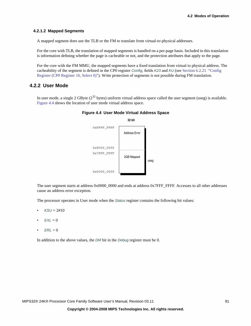
4.2 Modes of Operation
MIPS32® 24K® Processor Core Family Software User’s Manual, Revision 03.11 91
Copyright © 2004-2008 MIPS Technologies Inc. All rights reserved.
4.2.1.2 Mapped Segments
A mapped segment does use the TLB or the FM to translate from virtual-to-physical addresses.
For the core with TLB, the translation of mapped segments is handled on a per-page basis. Included in this translationis information defining whether the page is cacheable or not, and the protection attributes that apply to the page.
For the core with the FM MMU, the mapped segments have a fixed translation from virtual to physical address. Thecacheability of the segment is defined in the CP0 register Config, fields K23 and KU (see Section 6.2.21 “ConfigRegister (CP0 Register 16, Select 0)”). Write protection of segments is not possible during FM translation.
4.2.2 User Mode
In user mode, a single 2 GByte (231 bytes) uniform virtual address space called the user segment (useg) is available.Figure 4.4 shows the location of user mode virtual address space.
Figure 4.4 User Mode Virtual Address Space
The user segment starts at address 0x0000_0000 and ends at address 0x7FFF_FFFF. Accesses to all other addressescause an address error exception.
The processor operates in User mode when the Status register contains the following bit values:
• KSU = 2#10
• EXL = 0
• ERL = 0
In addition to the above values, the DM bit in the Debug register must be 0.
0x0000_0000
0x8000_0000
0x7FFF_FFFF
0xFFFF_FFFF
32 bit
Address Error
2GB Mappeduseg

Memory Management of the 24K® Core
92 MIPS32® 24K® Processor Core Family Software User’s Manual, Revision 03.11
Copyright © 2004-2008 MIPS Technologies Inc. All rights reserved.
Table 4.1 lists the characteristics of the User mode segment.
All valid user mode virtual addresses have their most significant bit cleared to 0, indicating that user mode can onlyaccess the lower half of the virtual memory map. Any attempt to reference an address with the most significant bit setwhile in user mode causes an address error exception.
The system maps all references to useg through the TLB or FM. For cores with a TLB, the virtual address is extendedwith the contents of the 8-bit ASID field to form a unique virtual address before translation. Also bit settings withinthe TLB entry for the page determine the cacheability of a reference. For FM MMU cores, the cacheability is set viathe KU field of the CP0 Config register.
4.2.3 Supervisor Mode
In supervisor mode, two virtual address spaces are available. A 2 GByte (231 bytes) uniform virtual address spacecalled the user segment (useg) as well as the 512MB (ksseg) are available. Figure 4.5 shows the location of supervisormode virtual address space.
Table 4.1 User Mode Segments
Address BitValue
Status Register
SegmentName Address Range Segment Size
Bit Value
EXL ERL KSU
32-bitA(31) = 0
0 0 2#10 useg 0x0000_0000 -->0x7FFF_FFFF
2 GByte
(231 bytes)

4.2 Modes of Operation
MIPS32® 24K® Processor Core Family Software User’s Manual, Revision 03.11 93
Copyright © 2004-2008 MIPS Technologies Inc. All rights reserved.
Figure 4.5 Supervisor Mode Virtual Address Space
The user segment starts at address 0x0000_0000 and ends at address 0x7FFF_FFFF. The supervisor segment beginsat 0xC000_0000 and ends at 0xDFFF_FFFF. Accesses to all other addresses cause an address error exception.
The processor operates in Supervisor mode when the Status register contains the following bit values:
• KSU = 2#01
• EXL = 0
• ERL = 0
In addition to the above values, the DM bit in the Debug register must be 0.
Address Error
Address Error
Supervisor virtual address spaceMapped, 512MB
Address Error
suseg
kseg0
kseg1
sseg
kseg3
Mapped, 2048MB
0x0000_0000
0x8000_0000
0xA000_0000
0xC000_0000
0xE000_0000
0x7FFF_FFFF
0x9FFF_FFFF
0xBFFF_FFFF
0xDFFF_FFFF
0xFFFF_FFFF

Memory Management of the 24K® Core
94 MIPS32® 24K® Processor Core Family Software User’s Manual, Revision 03.11
Copyright © 2004-2008 MIPS Technologies Inc. All rights reserved.
Table 4.1 lists the characteristics of the Supervisor mode segments.
The system maps all references to useg and ksseg through the TLB or FM. For cores with a TLB, the virtual addressis extended with the contents of the 8-bit ASID field to form a unique virtual address before translation. Also bit set-tings within the TLB entry for the page determine the cacheability of a reference. For FM MMU cores, the cacheabil-ity of useg and ksseg is set via the KU and K23 fields of the CP0 Config register respectively.
4.2.4 Kernel Mode
The processor operates in Kernel mode when the DM bit in the Debug register is 0 and the Status register contains oneor more of the following values:
• KSU = 2#00
• ERL = 1
• EXL = 1
When a non-debug exception is detected, EXL or ERL will be set and the processor will enter Kernel mode. At the endof the exception handler routine, an Exception Return (ERET) instruction is generally executed. The ERET instruc-tion jumps to the Exception PC, clears ERL, and clears EXL if ERL=0. This may return the processor to User mode.
Kernel mode virtual address space is divided into regions differentiated by the high-order bits of the virtual address,as shown in Figure 4.6. Also, Table 4.3 lists the characteristics of the Kernel mode segments.
Table 4.2 Supervisor Mode Segments
Address BitValue
Status Register
SegmentName Address Range Segment Size
Bit Value
EXL ERL KSU
32-bitA(31) = 0
0 0 2#01 suseg 0x0000_0000 -->0x7FFF_FFFF
2 GByte
(231 bytes)
32-bitA(31:29) = 1102
0 0 2#01 sseg 0xC000_0000 ->0xDFFF_FFFF
512MB
(229 bytes)
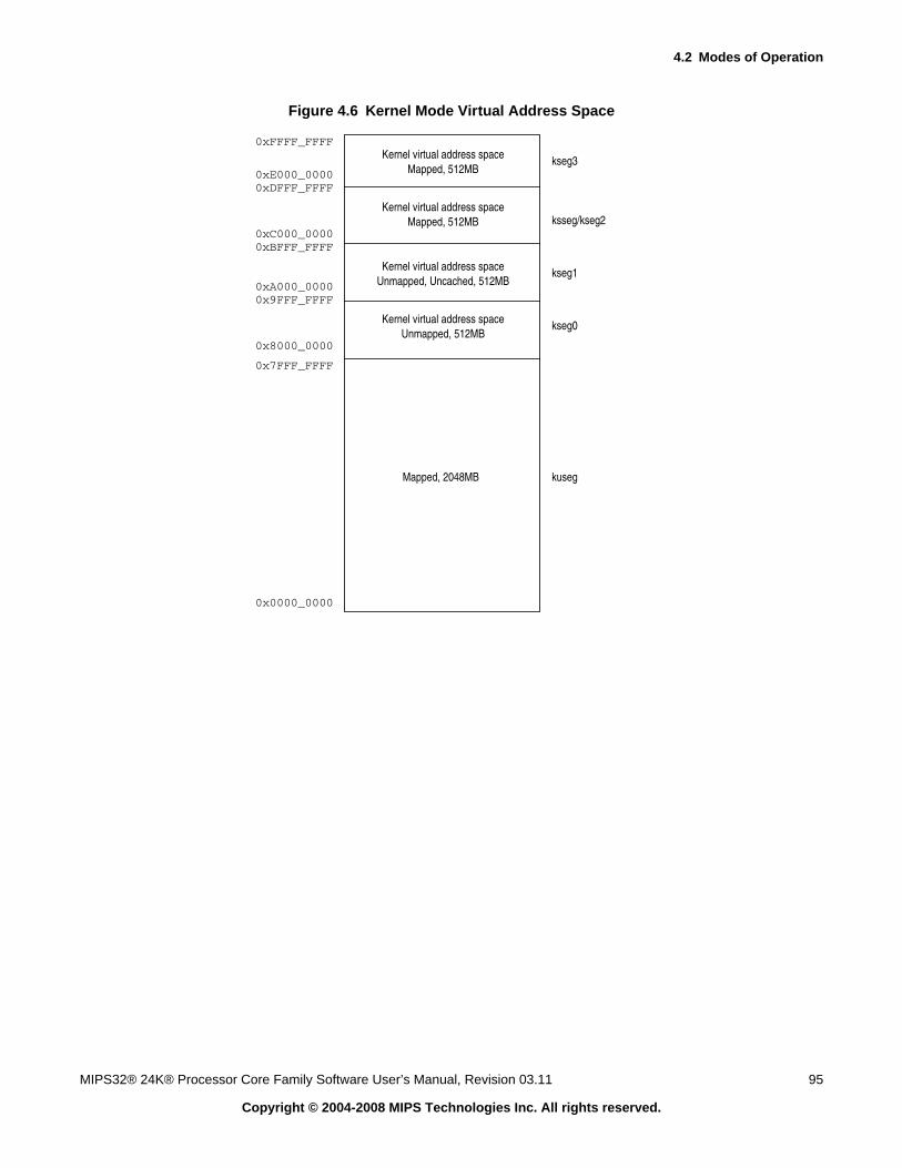
4.2 Modes of Operation
MIPS32® 24K® Processor Core Family Software User’s Manual, Revision 03.11 95
Copyright © 2004-2008 MIPS Technologies Inc. All rights reserved.
Figure 4.6 Kernel Mode Virtual Address Space
Kernel virtual address spaceUnmapped, 512MB
Kernel virtual address spaceUnmapped, Uncached, 512MB
Kernel virtual address spaceMapped, 512MB
Kernel virtual address spaceMapped, 512MB
kuseg
kseg0
kseg1
ksseg/kseg2
kseg3
Mapped, 2048MB
0x0000_0000
0x8000_0000
0xA000_0000
0xC000_0000
0xE000_0000
0x7FFF_FFFF
0x9FFF_FFFF
0xBFFF_FFFF
0xDFFF_FFFF
0xFFFF_FFFF

Memory Management of the 24K® Core
96 MIPS32® 24K® Processor Core Family Software User’s Manual, Revision 03.11
Copyright © 2004-2008 MIPS Technologies Inc. All rights reserved.
4.2.4.1 Kernel Mode, User Space (kuseg)
In Kernel mode, when the most-significant bit of the virtual address (A31) is cleared, the 32-bit kuseg virtual address
space is selected and covers the full 231 bytes (2 GBytes) of the current user address space mapped to addresses0x0000_0000 - 0x7FFF_FFFF. For cores with TLBs, the virtual address is extended with the contents of the 8-bitASID field to form a unique virtual address.
When ERL = 1 in the Status register, the user address region becomes a 231-byte unmapped and uncached addressspace. While in this setting, the kuseg virtual address maps directly to the same physical address, and does not includethe ASID field.
4.2.4.2 Kernel Mode, Kernel Space 0 (kseg0)
In Kernel mode, when the most-significant three bits of the virtual address are 1002, 32-bit kseg0 virtual address
space is selected; it is the 229-byte (512-MByte) kernel virtual space located at addresses 0x8000_0000 -0x9FFF_FFFF. References to kseg0 are unmapped; the physical address selected is defined by subtracting0x8000_0000 from the virtual address. The K0 field of the Config register controls cacheability.
4.2.4.3 Kernel Mode, Kernel Space 1 (kseg1)
In Kernel mode, when the most-significant three bits of the 32-bit virtual address are 1012, 32-bit kseg1 virtual
address space is selected. kseg1 is the 229-byte (512-MByte) kernel virtual space located at addresses 0xA000_0000 -0xBFFF_FFFF. References to kseg1 are unmapped; the physical address selected is defined by subtracting0xA000_0000 from the virtual address. Caches are disabled for accesses to these addresses, and physical memory (ormemory-mapped I/O device registers) are accessed directly.
Table 4.3 Kernel Mode Segments
Address BitValues
Status Register Is Oneof These Values
SegmentName Address Range Segment SizeKSU EXL ERL
A(31) = 0 (KSU = 002
orEXL = 1
orERL = 1)
andDM = 0
kuseg 0x0000_0000through
0x7FFF_FFFF
2 GBytes (231 bytes)
A(31:29) = 1002 kseg0 0x8000_0000through
0x9FFF_FFFF
512 MBytes (229
bytes)
A(31:29) = 1012 kseg1 0xA000_0000through
0xBFFF_FFFF
512 MBytes (229
bytes)
A(31:29) = 1102 ksseg/kseg2 0xC000_0000through
0xDFFF_FFFF
512 MBytes (229
bytes)
A(31:29) = 1112 kseg3 0xE000_0000through
0xFFFF_FFFF
512 MBytes (229
bytes)

4.2 Modes of Operation
MIPS32® 24K® Processor Core Family Software User’s Manual, Revision 03.11 97
Copyright © 2004-2008 MIPS Technologies Inc. All rights reserved.
4.2.4.4 Kernel Mode, Kernel/Supervisor Space 2 (ksseg/kseg2)
In Kernel mode, when KSU= 002, ERL = 1, or EXL = 1 in the Status register, and DM = 0 in the Debug register, andthe most-significant three bits of the 32-bit virtual address are 1102, 32-bit kseg2 virtual address space is selected.
With the FM MMU, this 229-byte (512-MByte) kernel virtual space is located at physical addresses 0xC000_0000 -0xDFFF_FFFF. Otherwise, this space is mapped through the TLB.
4.2.4.5 Kernel Mode, Kernel Space 3 (kseg3)
In Kernel mode, when the most-significant three bits of the 32-bit virtual address are 1112 , the kseg3 virtual address
space is selected. With the FM MMU, this 229-byte (512-MByte) kernel virtual space is located at physical addresses0xE000_0000 - 0xFFFF_FFFF. Otherwise, this space is mapped through the TLB.
4.2.5 Debug Mode
Debug mode address space is identical to Kernel mode address space with respect to mapped and unmapped areas,except for kseg3. In kseg3, a debug segment, dseg, co-exists in the virtual address range 0xFF20_0000 to0xFF3F_FFFF. The layout is shown in Figure 4.7.
Figure 4.7 Debug Mode Virtual Address Space
The dseg is subdivided into the dmseg segment at 0xFF20_0000 to 0xFF2F_FFFF, which is used when the probe ser-vices the memory segment, and the drseg segment at 0xFF30_0000 to 0xFF3F_FFFF which is used when mem-ory-mapped debug registers are accessed. The subdivision and attributes for the segments are shown in Table 4.4.
Accesses to memory that would normally cause an exception if tried from kernel mode cause the core to re-enterdebug mode via a debug mode exception. This includes accesses usually causing a TLB exception, with the result thatsuch accesses are not handled by the usual memory management routines.
0x0000_0000
0xFF20_0000
0xFF40_00000xFFFF_FFFF
dseg
kseg1
kseg0 Unmapped
Mapped if mapped in Kernel Mode
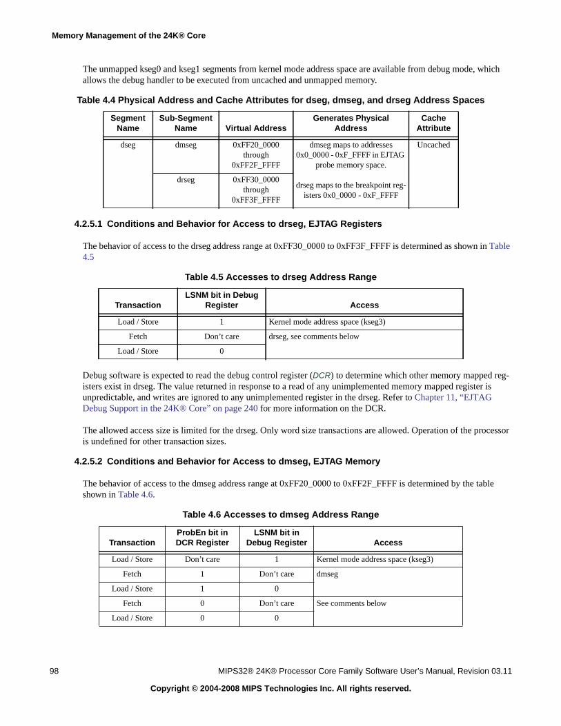
Memory Management of the 24K® Core
98 MIPS32® 24K® Processor Core Family Software User’s Manual, Revision 03.11
Copyright © 2004-2008 MIPS Technologies Inc. All rights reserved.
The unmapped kseg0 and kseg1 segments from kernel mode address space are available from debug mode, whichallows the debug handler to be executed from uncached and unmapped memory.
4.2.5.1 Conditions and Behavior for Access to drseg, EJTAG Registers
The behavior of access to the drseg address range at 0xFF30_0000 to 0xFF3F_FFFF is determined as shown in Table4.5
Debug software is expected to read the debug control register (DCR) to determine which other memory mapped reg-isters exist in drseg. The value returned in response to a read of any unimplemented memory mapped register isunpredictable, and writes are ignored to any unimplemented register in the drseg. Refer to Chapter 11, “EJTAGDebug Support in the 24K® Core” on page 240 for more information on the DCR.
The allowed access size is limited for the drseg. Only word size transactions are allowed. Operation of the processoris undefined for other transaction sizes.
4.2.5.2 Conditions and Behavior for Access to dmseg, EJTAG Memory
The behavior of access to the dmseg address range at 0xFF20_0000 to 0xFF2F_FFFF is determined by the tableshown in Table 4.6.
Table 4.4 Physical Address and Cache Attributes for dseg, dmseg, and drseg Address Spaces
SegmentName
Sub-SegmentName Virtual Address
Generates PhysicalAddress
CacheAttribute
dseg dmseg 0xFF20_0000through
0xFF2F_FFFF
dmseg maps to addresses0x0_0000 - 0xF_FFFF in EJTAG
probe memory space.
drseg maps to the breakpoint reg-isters 0x0_0000 - 0xF_FFFF
Uncached
drseg 0xFF30_0000through
0xFF3F_FFFF
Table 4.5 Accesses to drseg Address Range
TransactionLSNM bit in Debug
Register Access
Load / Store 1 Kernel mode address space (kseg3)
Fetch Don’t care drseg, see comments below
Load / Store 0
Table 4.6 Accesses to dmseg Address Range
TransactionProbEn bit inDCR Register
LSNM bit inDebug Register Access
Load / Store Don’t care 1 Kernel mode address space (kseg3)
Fetch 1 Don’t care dmseg
Load / Store 1 0
Fetch 0 Don’t care See comments below
Load / Store 0 0

4.3 Translation Lookaside Buffer
MIPS32® 24K® Processor Core Family Software User’s Manual, Revision 03.11 99
Copyright © 2004-2008 MIPS Technologies Inc. All rights reserved.
The case with access to the dmseg when the ProbEn bit in the DCR register is 0 is not expected to happen. Debugsoftware is expected to check the state of the ProbEn bit in DCR register before attempting to reference dmseg. Ifsuch a reference does happen, the reference hangs until it is satisfied by the probe. The probe can not assume thatthere will never be a reference to dmseg if the ProbEn bit in the DCR register is 0 because there is an inherent racebetween the debug software sampling the ProbEn bit as 1 and the probe clearing it to 0.
4.3 Translation Lookaside Buffer
The following subsections discuss the TLB memory management scheme used in the 24Kc processor core. The TLBconsists of the joint and micro address translation buffers:
• 16-64 dual-entry fully associative Joint TLB (JTLB)
• 4-entry fully associative Instruction micro TLB (ITLB)
• 8-entry fully associative Data micro TLB (DTLB)
4.3.1 Joint TLB
The 16-64 dual-entry, fully associative Joint TLB maps 32-128 virtual pages to their corresponding physicaladdresses. The purpose of the TLB is to translate virtual addresses and their corresponding ASID into a physicalmemory address. The translation is performed by comparing the upper bits of the virtual address (along with theASID bits) against each of the entries in the tag portion of the JTLB structure. Because this structure is used to trans-late both instruction and data virtual addresses, it is referred to as a “joint” TLB.
The JTLB is organized as 16-64 pairs of even and odd entries containing descriptions of pages that range in size from4-KBytes to 256MBytes into the 4-GByte physical address space.
The JTLB is organized in pairs of page entries to minimize its overall size. Each virtual tag entry corresponds to twophysical data entries, an even page entry and an odd page entry. The highest order virtual address bit not participatingin the tag comparison is used to determine which of the two data entries is used. Since page size can vary on apage-pair basis, the determination of which address bits participate in the comparison and which bit is used to makethe even-odd selection must be done dynamically during the TLB lookup.
Figure 4.8 shows the contents of one of the dual-entries in the JTLB. The bit range indication in the figure serves toclarify which address bits are (or may be) affected during the translation process.
Figure 4.8 JTLB Entry (Tag and Data)
PageMask[28:13]
D0
G ASID[7:0]
PFN0[31:12] C0[2:0]
D1PFN1[31:12] C1[2:0]
VPN2[31:13]
V0
V1
Tag Entry
Data Entries
19 1 8
20 3 1 1
G

Memory Management of the 24K® Core
100 MIPS32® 24K® Processor Core Family Software User’s Manual, Revision 03.11
Copyright © 2004-2008 MIPS Technologies Inc. All rights reserved.
Table 4.7 and Table 4.8 explain each of the fields in a JTLB entry.
Table 4.7 TLB Tag Entry Fields
Field Name Description
PageMask[28:13] Page Mask Value. The Page Mask defines the page size by masking the appropriateVPN2 bits from being involved in a comparison. It is also used to determine whichaddress bit is used to make the even-odd page (PFN0-PFN1) determination. See the tablebelow.
The PageMask column above shows all the legal values for PageMask. Because eachpair of bits can only have the same value, the physical entry in the JTLB will only save acompressed version of the PageMask using only 8 bits. This is however transparent tosoftware, which will always work with a 16 bit field
VPN2[31:13] Virtual Page Number divided by 2. This field contains the upper bits of the virtual pagenumber. Because it represents a pair of TLB pages, it is divided by 2. Bits 31:29 arealways included in the TLB lookup comparison. Bits 28:13 are included depending onthe page size, defined by PageMask
G Global Bit. When set, indicates that this entry is global to all processes and/or threadsand thus disables inclusion of the ASID in the comparison.
ASID[7:0] Address Space Identifier. Identifies which process or thread this TLB entry is associatedwith.
Table 4.8 TLB Data Entry Fields
Field Name Description
PFN0[31:12],PFN1[31:12]
Physical Frame Number. Defines the upper bits of the physical address.
PageMask Page Size Even/Odd Bank Select Bit
00_0000_0000_0000_00 4KB VAddr[12]
00_0000_0000_0000_11 16KB VAddr[14]
00_0000_0000_0011_11 64KB VAddr[16]
00_0000_0000_1111_11 256KB VAddr[18]
00_0000_0011_1111_11 1MB VAddr[20]
00_0000_1111_1111_11 4MB VAddr[22]
00_0011_1111_1111_11 16MB VAddr[24]
00_1111_1111_1111_11 64MB VAddr[26]
11_1111_1111_1111_11 256MB VAddr[28]
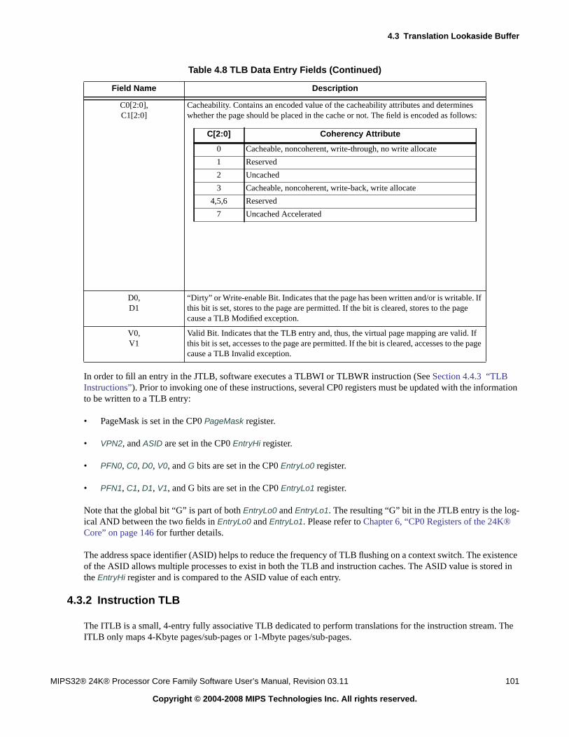
4.3 Translation Lookaside Buffer
MIPS32® 24K® Processor Core Family Software User’s Manual, Revision 03.11 101
Copyright © 2004-2008 MIPS Technologies Inc. All rights reserved.
In order to fill an entry in the JTLB, software executes a TLBWI or TLBWR instruction (See Section 4.4.3 “TLBInstructions”). Prior to invoking one of these instructions, several CP0 registers must be updated with the informationto be written to a TLB entry:
• PageMask is set in the CP0 PageMask register.
• VPN2, and ASID are set in the CP0 EntryHi register.
• PFN0, C0, D0, V0, and G bits are set in the CP0 EntryLo0 register.
• PFN1, C1, D1, V1, and G bits are set in the CP0 EntryLo1 register.
Note that the global bit “G” is part of both EntryLo0 and EntryLo1. The resulting “G” bit in the JTLB entry is the log-ical AND between the two fields in EntryLo0 and EntryLo1. Please refer to Chapter 6, “CP0 Registers of the 24K®Core” on page 146 for further details.
The address space identifier (ASID) helps to reduce the frequency of TLB flushing on a context switch. The existenceof the ASID allows multiple processes to exist in both the TLB and instruction caches. The ASID value is stored inthe EntryHi register and is compared to the ASID value of each entry.
4.3.2 Instruction TLB
The ITLB is a small, 4-entry fully associative TLB dedicated to perform translations for the instruction stream. TheITLB only maps 4-Kbyte pages/sub-pages or 1-Mbyte pages/sub-pages.
C0[2:0],C1[2:0]
Cacheability. Contains an encoded value of the cacheability attributes and determineswhether the page should be placed in the cache or not. The field is encoded as follows:
D0,D1
“Dirty” or Write-enable Bit. Indicates that the page has been written and/or is writable. Ifthis bit is set, stores to the page are permitted. If the bit is cleared, stores to the pagecause a TLB Modified exception.
V0,V1
Valid Bit. Indicates that the TLB entry and, thus, the virtual page mapping are valid. Ifthis bit is set, accesses to the page are permitted. If the bit is cleared, accesses to the pagecause a TLB Invalid exception.
Table 4.8 TLB Data Entry Fields (Continued)
Field Name Description
C[2:0] Coherency Attribute
0 Cacheable, noncoherent, write-through, no write allocate
1 Reserved
2 Uncached
3 Cacheable, noncoherent, write-back, write allocate
4,5,6 Reserved
7 Uncached Accelerated

Memory Management of the 24K® Core
102 MIPS32® 24K® Processor Core Family Software User’s Manual, Revision 03.11
Copyright © 2004-2008 MIPS Technologies Inc. All rights reserved.
The ITLB is managed by hardware and is transparent to software. If a fetch address cannot be translated by the ITLB,the JTLB is accessed trying to translate it in the following clock cycles. If successful, the translation information iscopied into the ITLB and bypassed to the tag comparators. This results in an ITLB miss penalty of at least 2 cycles.Depending on the JTLB implementation or if it is busy with other operations, it may take additional cycles.
4.3.3 Data TLB
The DTLB is a small 8-entry, fully associative TLB which provides a faster translation for Load/Store addresses thanis possible with the JTLB. The DTLB only maps 4-Kbyte pages/sub-pages or 1-Mbyte pages/sub-pages.
Like the ITLB, the DTLB is managed by hardware and is transparent to software. For simultaneous ITLB and DTLBmisses, the DTLB has priority and will access the JTLB first.
4.4 Virtual-to-Physical Address Translation
Converting a virtual address to a physical address begins by comparing the virtual address from the processor withthe virtual addresses in the TLB. There is a match when the VPN of the address is the same as the VPN field of theentry, and either:
• The Global (G) bit of both the even and odd pages of the TLB entry are set, or
• The ASID field of the virtual address is the same as the ASID field of the TLB entry
This match is referred to as a TLB hit. If there is no match, a TLB miss exception is taken by the processor and soft-ware is allowed to refill the TLB from a page table of virtual/physical addresses in memory.
Figure 4.9 shows the logical translation of a virtual address into a physical address.
In this figure the virtual address is extended with an 8-bit ASID, which reduces the frequency of TLB flushing duringa context switch. This 8-bit ASID contains the number assigned to that process and is stored in the CP0 EntryHi regis-ter.

4.4 Virtual-to-Physical Address Translation
MIPS32® 24K® Processor Core Family Software User’s Manual, Revision 03.11 103
Copyright © 2004-2008 MIPS Technologies Inc. All rights reserved.
Figure 4.9 Overview of a Virtual-to-Physical Address Translation
If there is a virtual address match in the TLB, the Physical Frame Number (PFN) is output from the TLB and concat-enated with the Offset, to form the physical address. The Offset represents an address within the page frame space. Asshown in Figure 4.9, the Offset does not pass through the TLB. Figure 4.10 shows a flow diagram of the address trans-lation process for two page sizes. The top portion of the figure shows a virtual address for a 4 KByte page size. Thewidth of the Offset is defined by the page size. The remaining 20 bits of the address represent the virtual page number(VPN). The bottom portion of Figure 4.10 shows the virtual address for a 16 MByte page size. The remaining 8 bitsof the address represent the VPN.
1.Virtual address (VA) represented by the virtual pagenumber (VPN) is compared with tag in TLB.
2. If there is a match, the page frame number(PFN0 or PFN1) representing the upper bits of thephysical address (PA) is output from the TLB theTLB.
3. The Offset, which does not pass through the TLB, isthen concatenated with the PFN.
OffsetVPNG ASID
Virtual Address
TLBEntry
OffsetPFN
TLB
G ASID VPN2
C0 D0 V0 PFN0
PFN1C1 D1 V1
Physical Address

Memory Management of the 24K® Core
104 MIPS32® 24K® Processor Core Family Software User’s Manual, Revision 03.11
Copyright © 2004-2008 MIPS Technologies Inc. All rights reserved.
Figure 4.10 32-bit Virtual Address Translation
4.4.1 Hits, Misses, and Multiple Matches
Each JTLB entry contains a tag and two data fields. If a match is found, the upper bits of the virtual address arereplaced with the page frame number (PFN) stored in the corresponding entry in the data array of the JTLB. Thegranularity of JTLB mappings is defined in terms of TLB pages. The JTLB supports pages of different sizes rangingfrom 4KB to 256 MB in powers of 4. If a match is found, but the entry is invalid (i.e., the V bit in the data field is 0),a TLB Invalid exception is taken.
If no match occurs (TLB miss), an exception is taken and software refills the TLB from the page table resident inmemory. Figure 4.11 shows the translation and exception flow of the TLB.
Software can write over a selected TLB entry or use a hardware mechanism to write into a random entry. TheRandom register selects which TLB entry to use on a TLBWR. This register decrements almost every cycle, wrap-ping to the maximum once its value is equal to the Wired register. Thus, TLB entries below the Wired value cannot bereplaced by a TLBWR allowing important mappings to be preserved. In order to reduce the possibility for a livelocksituation, the Random register includes a 10-bit LFSR that introduces a pseudo-random perturbation into the decre-ment.
The core implements a TLB write-compare mechanism to ensure that multiple TLB matches do not occur. On theTLB write operation, the VPN2 field to be written is compared with all other entries in the TLB. If a match occurs, theentry in the TLB is valid, and the entry being written is valid, the core takes a machine-check exception, sets the TSbit in the CP0 Status register, and aborts the write operation. For further details on exceptions, please refer to Chapter5, “Exceptions and Interrupts in the 24K® Core” on page 110. There is a hidden bit in each TLB entry that is clearedon a Reset. This bit is set once the TLB entry is written and is included in the match detection. Therefore, uninitial-ized TLB entries will not cause a TLB shutdown.
Compared with previous cores from MIPS Technologies, the 24K core uses a more relaxed check for multiplematches in order to avoid machine check exceptions while flushing or initializing the TLB. On a write, all matchingentries are disabled to prevent them from matching on future compares. A machine check is only signaled if the entry
11Virtual address with 1M (220) 4-KByte pages
Virtual Address with 256 (28)16-MByte pages
8 bits = 256 pages
20 bits = 1M pages
Virtual-to-physicaltranslation in TLB
Bit 31 of the virtual addressselects user and kernel addressspaces.
Offset passed unchanged tophysical memory.
Virtual-to-physicaltranslation in TLB
Offset passed unchanged tophysical memory.
32-bit Physical Address
ASID VPN Offset
PFN0/1 Offset
TLB
TLB
ASID VPN Offset0233132 2439
313239 012
031
8 8 24
8 20 12

4.4 Virtual-to-Physical Address Translation
MIPS32® 24K® Processor Core Family Software User’s Manual, Revision 03.11 105
Copyright © 2004-2008 MIPS Technologies Inc. All rights reserved.
being written has its valid bit set, the matching entry in the TLB has its valid bit set, and the matching entry is not theentry being written. The cases for the signalling of the machine check exception are enumerated in Table 4.9.
4.4.2 Memory Space
To assist in controlling both the amount of mapped space and the replacement characteristics of various memoryregions, the 24K core provides two mechanisms.
4.4.2.1 Page Sizes
First, the page size can be configured, on a per entry basis, to map different page sizes ranging from 4 KByte to 256MByte, in multiples of 4. The CP0 PageMask register is loaded with the desired page size, which is then entered intothe TLB when a new entry is written. Thus, operating systems can provide special-purpose maps. For example, a typ-ical frame buffer can be memory mapped with only one TLB entry.
The 24K core implements the following page sizes:
4K, 16K, 64K, 256K, 1M, 4M, 16M, 64M, 256M.
Software may determine which page sizes are supported by writing all ones to the CP0 PageMask register, then read-ing the value back. For additional information, see Section 6.2.5 “UserLocal Register (CP0 Register 4, Select 2)”.
4.4.2.2 Replacement Algorithm
The second mechanism controls the replacement algorithm when a TLB miss occurs. To select a TLB entry to bewritten with a new mapping, the 24K core provides a random replacement algorithm. However, the processor alsoprovides a mechanism whereby a programmable number of mappings can be locked into the TLB via the CP0 Wiredregister, thus avoiding random replacement. Please refer to Section 6.2.7 “Wired Register (CP0 Register 6, Select 0)”for further details.
Table 4.9 Machine Check Exception
ExistingMatch
Matching Entry equalsWritten Entry
Existing PageValid Bit
Written PageValid Bit
MachineCheck?
No X X X No
Yes Yes X X No
Yes No 0 0 No
Yes No 0 1 No
Yes No 1 0 No
Yes No 1 1 Yes

Memory Management of the 24K® Core
106 MIPS32® 24K® Processor Core Family Software User’s Manual, Revision 03.11
Copyright © 2004-2008 MIPS Technologies Inc. All rights reserved.
Figure 4.11 TLB Address Translation Flow in the 24K® Processor Core
4.4.3 TLB Instructions
Table 4.10 lists the TLB-related instructions. Refer to Chapter 12, “24K® Processor Core Instructions” on page 303for more information on these instructions.
Table 4.10 TLB Instructions
Op Code Description of Instruction
TLBP Translation Lookaside Buffer Probe
TLBR Translation Lookaside Buffer Read
For valid address space,see the section describingModes of operation in thischapter.
Virtual Address (Input)
VPN andASID
UserMode?
NoYes
No
Yes
No
Yes
No
No No
No
No
No
No
Yes
Yes Yes
Yes
Yes
Yes
Yes
Exception
Global
Valid
Dirty
Noncacheable
Physical Address (Output)
UserAddress?
AddressError
UnmappedAddress
kseg0/kseg1Address
VPNMatch?
G = 1?
C=010 orC=111?
ASIDMatch?
V = 1?
D = 1? Write?
TLBModified
TLBInvalid
TLB Refill
AccessCache
AccessMain
Memory

4.5 Fixed Mapping MMU
MIPS32® 24K® Processor Core Family Software User’s Manual, Revision 03.11 107
Copyright © 2004-2008 MIPS Technologies Inc. All rights reserved.
4.5 Fixed Mapping MMU
The 24K core optionally implements a simple Fixed Mapping (FM) memory management unit that is smaller than thea full translation lookaside buffer (TLB) and more easily synthesized. Like a TLB, the FM performs virtual-to-physi-cal address translation and provides attributes for the different memory segments. Those memory segments which areunmapped in a TLB implementation (kseg0 and kseg1) are translated identically by the FM MMU.
The FM also determines the cacheability of each segment. These attributes are controlled via bits in the Config regis-ter. Table 4.11 shows the encoding for the K23 (bits 30:28), KU (bits 27:25) and K0 (bits 2:0) of the Config register.
With the FM MMU, no translation exceptions can be taken, although address errors are still possible.
The FM performs a simple translation to map from virtual addresses to physical addresses. This mapping is shown inFigure 4.12. When ERL=1, useg and kuseg become unmapped and uncached just like they do if there is a TLB. TheERL mapping is shown in Figure 4.13.
TLBWI Translation Lookaside Buffer Write Index
TLBWR Translation Lookaside Buffer Write Random
Table 4.11 Cache Coherency Attributes
Config Register FieldsK23, KU, and K0 Cache Coherency Attribute
0 Cacheable, noncoherent, write-through, no write allocate
1 Reserved
2 Uncached
3 Cacheable, noncoherent, write-back, write allocate
4,5,6 Reserved
7 Uncached Accelerated
Table 4.12 Cacheability of Segments with Fixed Mapping Translation
SegmentVirtual Address
Range Cacheability
useg/kuseg 0x0000_0000-0x7FFF_FFFF
Controlled by the KU field (bits 27:25) of the Config register. Referto Table 4.11 for the encoding.
kseg0 0x8000_0000-0x9FFF_FFFF
Controlled by the K0 field (bits 2:0) of the Config register. SeeTable 4.11 for the encoding.
kseg1 0xA000_0000-0xBFFF_FFFF
Always uncacheable
kseg2 0xC000_0000-0xDFFF_FFFF
Controlled by the K23 field (bits 30:28) of the Config register.Refer to Table 4.11 for the encoding.
kseg3 0xE000_0000-0xFFFF_FFFF
Controlled by K23 field (bits 30:28) of the Config register. Refer toTable 4.11 for the encoding.
Table 4.10 TLB Instructions (Continued)
Op Code Description of Instruction

Memory Management of the 24K® Core
108 MIPS32® 24K® Processor Core Family Software User’s Manual, Revision 03.11
Copyright © 2004-2008 MIPS Technologies Inc. All rights reserved.
The ERL bit is usually never asserted by software. It is asserted by hardware after a Reset, NMI, or Cache Error. SeeSection 5.8 “Exceptions” for further information on exceptions.
Figure 4.12 FM Memory Map (ERL=0) in the 24K® Processor Core
useg/kuseg
useg/kuseg
Virtual Address Physical Address
kseg3
kseg2
kseg1
kseg0
kseg3
kseg2
reserved
kseg0/kseg1
0xE000_0000
0xC000_0000
0xA000_0000
0x8000_0000
0x0000_0000
0xE000_0000
0xC000_0000
0x0000_0000
0x2000_0000
0x4000_0000
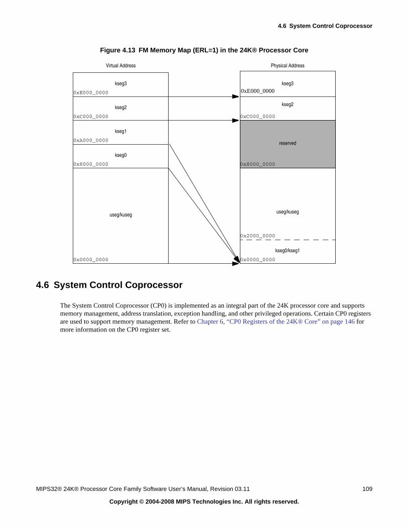
4.6 System Control Coprocessor
MIPS32® 24K® Processor Core Family Software User’s Manual, Revision 03.11 109
Copyright © 2004-2008 MIPS Technologies Inc. All rights reserved.
Figure 4.13 FM Memory Map (ERL=1) in the 24K® Processor Core
4.6 System Control Coprocessor
The System Control Coprocessor (CP0) is implemented as an integral part of the 24K processor core and supportsmemory management, address translation, exception handling, and other privileged operations. Certain CP0 registersare used to support memory management. Refer to Chapter 6, “CP0 Registers of the 24K® Core” on page 146 formore information on the CP0 register set.
0xE000_0000
Physical AddressVirtual Address
kseg3
0xE000_0000
kseg3
kseg2kseg2
0xC000_00000xC000_0000
0xA000_0000
kseg1
reserved
0x8000_00000x8000_0000
kseg0
useg/kuseguseg/kuseg
0x2000_0000
0x0000_00000x0000_0000
kseg0/kseg1
Chapter 5
MIPS32® 24K® Processor Core Family Software User’s Manual, Revision 03.11 110
Copyright © 2004-2008 MIPS Technologies Inc. All rights reserved.
Exceptions and Interrupts in the 24K® Core
Programs executing on the 24K processor core receive exceptions from a number of sources, including translationlookaside buffer (TLB) misses, arithmetic overflows, I/O interrupts, and system calls. When one of these exceptionsis detected, the normal sequence of instruction execution is suspended and the processor enters kernel mode.
In kernel mode interrupts are disabled and a software exception processor (also called a handler), located at a specificiaddress, is executed. The handler saves the context of the processor, including the contents of the program counter,the current operating mode, and the status of the interrupts (enabled or disabled). This context is saved so it can berestored when the exception has been serviced.
When an exception occurs, the Exception Program Counter (EPC) register is loaded with a location where executioncan restart after the exception has been serviced. Most exceptions are precise, which mean that EPC can be used toidentify the instruction that caused the exception. For precise exceptions the restart location in the EPC register is theaddress of the instruction that caused the exception or, if the instruction was executing in a branch delay slot, theaddress of the branch instruction immediately preceding the delay slot. To distinguish between the two, software mustread the BD bit in the CP0 Cause register. Bus error exceptions and CP2 exceptions may be imprecise. For impreciseexceptions the instruction that caused the exception can not be identified.
This chapter contains the following sections:
• Section 5.1 “Exception Conditions”
• Section 5.2 “Exception Priority”
• Section 5.3 “Interrupts”
• Section 5.4 “GPR Shadow Registers”
• Section 5.5 “Exception Vector Locations”
• Section 5.6 “General Exception Processing”
• Section 5.7 “Debug Exception Processing”
• Section 5.8 “Exceptions”
• Section 5.9 “Exception Handling and Servicing Flowcharts”
5.1 Exception Conditions
When an exception condition occurs, the relevant instruction and all those that follow it in the pipeline are cancelled.Accordingly, any stall conditions and any later exception conditions that may have referenced this instruction areinhibited; there is no benefit in servicing stalls for a cancelled instruction.

5.2 Exception Priority
MIPS32® 24K® Processor Core Family Software User’s Manual, Revision 03.11 111
Copyright © 2004-2008 MIPS Technologies Inc. All rights reserved.
When an exception condition is detected on an instruction fetch, the core aborts that instruction and all instructionsthat follow. When this instruction reaches the WB stage, the exception flag causes it to write various CP0 registerswith the exception state, change the current program counter (PC) to the appropriate exception vector address, andclear the exception bits of earlier pipeline stages.
For most exception types this implementation allows all preceding instructions to complete execution and prevents allsubsequent instructions from completing. Thus, the value in the EPC (ErrorEPC for errors, or DEPC for debug excep-tions) is sufficient to restart execution. It also ensures that exceptions are taken in the order of execution; an instruc-tion taking an exception may itself be killed by an instruction further down the pipeline that takes an exception in alater cycle.
A number of exceptions can be taken imprecisely - that is, they are taken after the instruction that caused them hascompleted and potentially after following instructions have completed.
5.2 Exception Priority
Table 5.1 lists all possible exceptions, and the relative priority of each, highest to lowest. Several of these exceptionscan happen simultaneously, in that event the exception with the highest priority is the one taken.
Table 5.1 Priority of Exceptions
Exception Description
Reset Assertion of SI_Reset signal.
DSS EJTAG Debug Single Step.
DINT EJTAG Debug Interrupt. Caused by the assertion of the external EJ_DINT input, or bysetting the EjtagBrk bit in the ECR register.
DDBLImpr/DDBSImpr Debug Data Break Load/Store Imprecise
NMI Asserting edge of SI_NMI signal.
Machine Check TLB write that conflicts with an existing entry.
Interrupt Assertion of unmasked hardware or software interrupt signal.
Deferred Watch Deferred Watch (unmasked by K|DM->!(K|DM) transition).
DIB EJTAG debug hardware instruction break matched.
WATCH A reference to an address in one of the watch registers (fetch).
AdEL Fetch address alignment error.Fetch reference to protected address.
TLBL Fetch TLB missFetch TLB hit to page with V=0
ICache Error Parity error on ICache access
IBE Instruction fetch bus error.
DBp EJTAG Breakpoint (execution of SDBBP instruction).
Sys Execution of SYSCALL instruction.
Bp Execution of BREAK instruction.
CpU Execution of a coprocessor instruction for a coprocessor that is not enabled.
CEU Execution of a CorExtend instruction modifying local state when CorExtend is notenabled.
RI Execution of a Reserved Instruction.

Exceptions and Interrupts in the 24K® Core
112 MIPS32® 24K® Processor Core Family Software User’s Manual, Revision 03.11
Copyright © 2004-2008 MIPS Technologies Inc. All rights reserved.
5.3 Interrupts
Older 32-bit cores available from MIPS that implemented Release 1 of the Architecture included support for two soft-ware interrupts, six hardware interrupts, and a special-purpose timer interrupt. The timer interrupt was providedexternal to the core and typically combined with hardware interrupt 5 in an system-dependent manner. Interruptswere handled either through the general exception vector (offset 16#180) or the special interrupt vector (16#200),based on the value of CauseIV. Software was required to prioritize interrupts as a function of the CauseIP bits in theinterrupt handler prologue.
Release 2 of the Architecture, implemented by the 24K core, adds an upward-compatible extension to the Release 1interrupt architecture that supports vectored interrupts. In addition, Release 2 adds a new interrupt mode that supportsthe use of an external interrupt controller by changing the interrupt architecture.
Additionally, internal performance counters were added to the 24K core. These counters can be set up to count vari-ous events within the core. When the MSB of the counter gets set, it can trigger a performance counter interrupt. Thisis handled like the timer interrupt - it is an output of the core and can be brought back into the core’s interrupt pins ina system dependent manner.
5.3.1 Interrupt Modes
The 24K core includes support for three interrupt modes, as defined by Release 2 of the Architecture:
• Interrupt compatibility mode, which acts identically to that in an implementation of Release 1 of the Architec-ture.
FPE Floating Point exception
C2E Coprocessor2 Exception
IS1 Implementation specific Coprocessor2 exception
Ov Execution of an arithmetic instruction that overflowed.
Tr Execution of a trap (when trap condition is true).
DDBL / DDBS EJTAG Data Address Break (address only)
WATCH A reference to an address in one of the watch registers (data).
AdEL Load address alignment error.Load reference to protected address.
AdES Store address alignment error.Store to protected address.
TLBL Load TLB miss.Load TLB hit to page with V=0
TLBS Store TLB miss.Store TLB hit to page with V=0
TLB Mod Store to TLB page with D=0.
DCache Error Cache parity error - imprecise
L2 Cache Error L2 Cache ECC error - imprecise
DBE Load or store bus error - imprecise
Table 5.1 Priority of Exceptions (Continued)
Exception Description

5.3 Interrupts
MIPS32® 24K® Processor Core Family Software User’s Manual, Revision 03.11 113
Copyright © 2004-2008 MIPS Technologies Inc. All rights reserved.
• Vectored Interrupt (VI) mode, which adds the ability to prioritize and vector interrupts to a handler dedicated tothat interrupt, and to assign a GPR shadow set for use during interrupt processing. The presence of this mode isdenoted by the VInt bit in the Config3 register. This mode is architecturally optional; but it is always present onthe 24K core, so the VInt bit will always read as a 1 for the 24K core.
• External Interrupt Controller (EIC) mode, which redefines the way in which interrupts are handled to provide fullsupport for an external interrupt controller handling prioritization and vectoring of interrupts. This presence ofthis mode denoted by the VEIC bit in the Config3 register. Again, this mode is architecturally optional. On the24K core, the VEIC bit is set externally by the static input, SI_EICPresent, to allow system logic to indicate thepresence of an external interrupt controller.
The reset state of the processor is to interrupt compatibility mode such that a processor supporting Release 2 of theArchitecture, like the 24K core, is fully compatible with implementations of Release 1 of the Architecture.
Table 5.2 shows the current interrupt mode of the processor as a function of the coprocessor 0 register fields that canaffect the mode.
5.3.1.1 Interrupt Compatibility Mode
This is the default interrupt mode for the processor and is entered when a Reset exception occurs. In this mode, inter-rupts are non-vectored and dispatched though exception vector offset 16#180 (if CauseIV = 0) or vector offset16#200 (if CauseIV = 1). This mode is in effect if any of the following conditions are true:
• CauseIV = 0
• StatusBEV = 1
• IntCtlVS = 0, which would be the case if vectored interrupts are not implemented, or have been disabled.
A typical software handler for interrupt compatibility mode might look as follows:
/* * Assumptions: * - CauseIV = 1 (if it were zero, the interrupt exception would have to
Table 5.2 Interrupt Modes
Sta
tus B
EV
Cau
seIV
IntC
tlV
S
Co
nfi
g3 V
INT
Co
nfi
g3 V
EIC
Interrupt Mode
1 x x x x Compatibility
x 0 x x x Compatibility
x x =0 x x Compatibility
0 1 ≠0 1 0 Vectored Interrupt
0 1 ≠0 x 1 External Interrupt Controller
0 1 ≠0 0 0 Can’t happen - IntCtlVS can not be non-zero if neither
Vectored Interrupt nor External Interrupt Controller modeis implemented.
“x” denotes don’t care
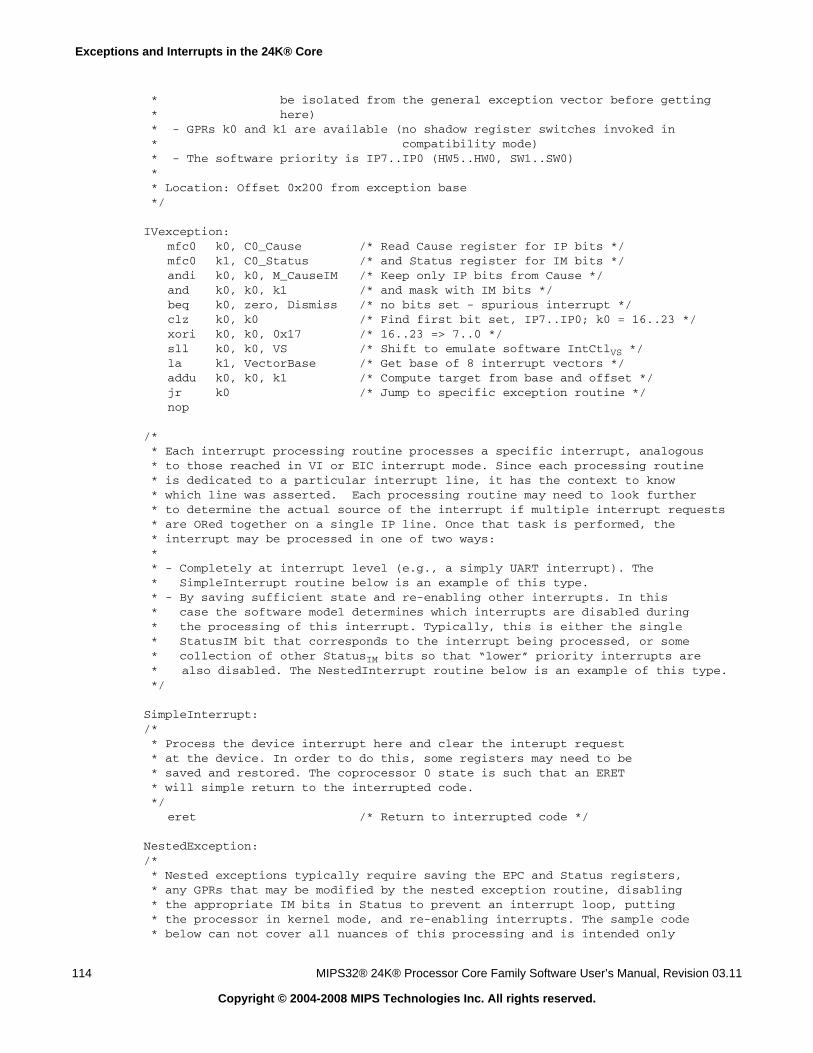
Exceptions and Interrupts in the 24K® Core
114 MIPS32® 24K® Processor Core Family Software User’s Manual, Revision 03.11
Copyright © 2004-2008 MIPS Technologies Inc. All rights reserved.
* be isolated from the general exception vector before getting * here) * - GPRs k0 and k1 are available (no shadow register switches invoked in * compatibility mode) * - The software priority is IP7..IP0 (HW5..HW0, SW1..SW0) * * Location: Offset 0x200 from exception base */
IVexception:mfc0 k0, C0_Cause /* Read Cause register for IP bits */mfc0 k1, C0_Status /* and Status register for IM bits */andi k0, k0, M_CauseIM /* Keep only IP bits from Cause */and k0, k0, k1 /* and mask with IM bits */beq k0, zero, Dismiss /* no bits set - spurious interrupt */clz k0, k0 /* Find first bit set, IP7..IP0; k0 = 16..23 */xori k0, k0, 0x17 /* 16..23 => 7..0 */sll k0, k0, VS /* Shift to emulate software IntCtlVS */la k1, VectorBase /* Get base of 8 interrupt vectors */addu k0, k0, k1 /* Compute target from base and offset */jr k0 /* Jump to specific exception routine */nop
/* * Each interrupt processing routine processes a specific interrupt, analogous * to those reached in VI or EIC interrupt mode. Since each processing routine * is dedicated to a particular interrupt line, it has the context to know * which line was asserted. Each processing routine may need to look further * to determine the actual source of the interrupt if multiple interrupt requests * are ORed together on a single IP line. Once that task is performed, the * interrupt may be processed in one of two ways: * * - Completely at interrupt level (e.g., a simply UART interrupt). The * SimpleInterrupt routine below is an example of this type. * - By saving sufficient state and re-enabling other interrupts. In this * case the software model determines which interrupts are disabled during * the processing of this interrupt. Typically, this is either the single * StatusIM bit that corresponds to the interrupt being processed, or some * collection of other StatusIM bits so that “lower” priority interrupts are * also disabled. The NestedInterrupt routine below is an example of this type. */
SimpleInterrupt:/* * Process the device interrupt here and clear the interupt request * at the device. In order to do this, some registers may need to be * saved and restored. The coprocessor 0 state is such that an ERET * will simple return to the interrupted code. */
eret /* Return to interrupted code */
NestedException:/* * Nested exceptions typically require saving the EPC and Status registers, * any GPRs that may be modified by the nested exception routine, disabling * the appropriate IM bits in Status to prevent an interrupt loop, putting * the processor in kernel mode, and re-enabling interrupts. The sample code * below can not cover all nuances of this processing and is intended only

5.3 Interrupts
MIPS32® 24K® Processor Core Family Software User’s Manual, Revision 03.11 115
Copyright © 2004-2008 MIPS Technologies Inc. All rights reserved.
* to demonstrate the concepts. */
/* Save GPRs here, and setup software context */mfc0 k0, C0_EPC /* Get restart address */sw k0, EPCSave /* Save in memory */mfc0 k0, C0_Status /* Get Status value */sw k0, StatusSave /* Save in memory */li k1, ~IMbitsToClear /* Get Im bits to clear for this interrupt */
/* this must include at least the IM bit *//* for the current interrupt, and may include *//* others */
and k0, k0, k1 /* Clear bits in copy of Status */ins k0, zero, S_StatusEXL, (W_StatusKSU+W_StatusERL+W_StatusEXL)
/* Clear KSU, ERL, EXL bits in k0 */mtc0 k0, C0_Status /* Modify mask, switch to kernel mode, */
/* re-enable interrupts */
/* * Process interrupt here, including clearing device interrupt. * In some environments this may be done with a thread running in * kernel or user mode. Such an environment is well beyond the scope of * this example. */
/* * To complete interrupt processing, the saved values must be restored * and the original interrupted code restarted. */
di /* Disable interrupts - may not be required */lw k0, StatusSave /* Get saved Status (including EXL set) */lw k1, EPCSave /* and EPC */mtc0 k0, C0_Status /* Restore the original value */mtc0 k1, C0_EPC /* and EPC *//* Restore GPRs and software state */eret /* Dismiss the interrupt */
5.3.1.2 Vectored Interrupt Mode
Vectored Interrupt mode builds on the interrupt compatibility mode by adding a priority encoder to prioritize pendinginterrupts and to generate a vector with which each interrupt can be directed to a dedicated handler routine. Thismode also allows each interrupt to be mapped to a GPR shadow set for use by the interrupt handler. Vectored Inter-rupt mode is in effect if all of the following conditions are true:
• Config3VInt = 1
• Config3VEIC = 0
• IntCtlVS ≠ 0
• CauseIV = 1
• StatusBEV = 0

Exceptions and Interrupts in the 24K® Core
116 MIPS32® 24K® Processor Core Family Software User’s Manual, Revision 03.11
Copyright © 2004-2008 MIPS Technologies Inc. All rights reserved.
In VI interrupt mode, the six hardware interrupts are interpreted as individual hardware interrupt requests. The timerand performance counter interrupts are combined in a system-dependent way (external to the core) with the hardwareinterrupts (the interrupt with which they are combined is indicated by the IntCtlIPTI/IPCI fields) to provide the appro-priate relative priority of the those interrupts with that of the hardware interrupts. The processor interrupt logic ANDseach of the CauseIP bits with the corresponding StatusIM bits. If any of these values is 1, and if interrupts are enabled(StatusIE = 1, StatusEXL = 0, and StatusERL = 0), an interrupt is signaled and a priority encoder scans the values inthe order shown in Table 5.3.
The priority order places a relative priority on each hardware interrupt and places the software interrupts at a prioritylower than all hardware interrupts. When the priority encoder finds the highest priority pending interrupt, it outputsan encoded vector number that is used in the calculation of the handler for that interrupt, as described below. This isshown pictorially in Figure 5.1.
Table 5.3 Relative Interrupt Priority for Vectored Interrupt Mode
RelativePriority
InterruptType
InterruptSource
InterruptRequest
Calculated From
Vector NumberGenerated by
Priority Encoder
Highest Priority Hardware HW5 IP7 and IM7 7
HW4 IP6 and IM6 6
HW3 IP5 and IM5 5
HW2 IP4 and IM4 4
HW1 IP3 and IM3 3
HW0 IP2 and IM2 2
Software SW1 IP1 and IM1 1
Lowest Priority SW0 IP0 and IM0 0

5.3 Interrupts
MIPS32® 24K® Processor Core Family Software User’s Manual, Revision 03.11 117
Copyright © 2004-2008 MIPS Technologies Inc. All rights reserved.
Figure 5.1 Interrupt Generation for Vectored Interrupt Mode
A typical software handler for vectored interrupt mode bypasses the entire sequence of code following the IVexcep-tion label shown for the compatibility mode handler above. Instead, the hardware performs the prioritization, dis-patching directly to the interrupt processing routine. Unlike the compatibility mode examples, a vectored interrupthandler may take advantage of a dedicated GPR shadow set to avoid saving any registers. As such, the SimpleInter-rupt code shown above need not save the GPRs.
A nested interrupt is similar to that shown for compatibility mode, but may also take advantage of running the nestedexception routine in the GPR shadow set dedicated to the interrupt or in another shadow set. Such a routine mightlook as follows:
NestedException:/* * Nested exceptions typically require saving the EPC, Status and SRSCtl registers, * setting up the appropriate GPR shadow set for the routine, disabling * the appropriate IM bits in Status to prevent an interrupt loop, putting * the processor in kernel mode, and re-enabling interrupts. The sample code * below can not cover all nuances of this processing and is intended only * to demonstrate the concepts. */
/* Use the current GPR shadow set, and setup software context */mfc0 k0, C0_EPC /* Get restart address */sw k0, EPCSave /* Save in memory */mfc0 k0, C0_Status /* Get Status value */sw k0, StatusSave /* Save in memory */mfc0 k0, C0_SRSCtl /* Save SRSCtl if changing shadow sets */sw k0, SRSCtlSaveli k1, ~IMbitsToClear /* Get Im bits to clear for this interrupt */
/* this must include at least the IM bit */
IP7
IP6
IP5
IP4
IP3
IP2
IP1
IP0
IM7
IM6
IM5
IM4
IM3
IM2
IM1
IM0
Prio
rity
Enco
de
HW5
HW4
HW3
HW2
HW1
HW0
Com
bine
CauseTI
StatusIE
InterruptRequest
VectorNumber
Latch Mask Encode
Any Request
Offs
et G
ener
ator
IntCtlVS
ExceptionVector Offset
Generate
SRSMap
Shadow SetNumber
IntCtlIPTI
CausePCI
IntCtlIPPCI

Exceptions and Interrupts in the 24K® Core
118 MIPS32® 24K® Processor Core Family Software User’s Manual, Revision 03.11
Copyright © 2004-2008 MIPS Technologies Inc. All rights reserved.
/* for the current interrupt, and may include *//* others */
and k0, k0, k1 /* Clear bits in copy of Status *//* If switching shadow sets, write new value to SRSCtlPSS here */ins k0, zero, S_StatusEXL, (W_StatusKSU+W_StatusERL+W_StatusEXL)
/* Clear KSU, ERL, EXL bits in k0 */mtc0 k0, C0_Status /* Modify mask, switch to kernel mode, */
/* re-enable interrupts *//* * If switching shadow sets, clear only KSU above, write target * address to EPC, and do execute an eret to clear EXL, switch * shadow sets, and jump to routine */
/* Process interrupt here, including clearing device interrupt */
/* * To complete interrupt processing, the saved values must be restored * and the original interrupted code restarted. */
di /* Disable interrupts - may not be required */lw k0, StatusSave /* Get saved Status (including EXL set) */lw k1, EPCSave /* and EPC */mtc0 k0, C0_Status /* Restore the original value */lw k0, SRSCtlSave /* Get saved SRSCtl */mtc0 k1, C0_EPC /* and EPC */mtc0 k0, C0_SRSCtl /* Restore shadow sets */ehb /* Clear hazard */eret /* Dismiss the interrupt */
5.3.1.3 External Interrupt Controller Mode
External Interrupt Controller Mode redefines the way that the processor interrupt logic is configured to provide sup-port for an external interrupt controller. The interrupt controller is responsible for prioritizing all interrupts, includinghardware, software, timer, and performance counter interrupts, and directly supplying to the processor the vectornumber of the highest priority interrupt. EIC interrupt mode is in effect if all of the following conditions are true:
• Config3VEIC = 1
• IntCtlVS ≠ 0
• CauseIV = 1
• StatusBEV = 0
In EIC interrupt mode, the processor sends the state of the software interrupt requests (CauseIP1..IP0) and the timerand performance counter interrupt requests (CauseTI/PCI) to the external interrupt controller, where it prioritizes theseinterrupts in a system-dependent way with other hardware interrupts. The interrupt controller can be a hard-wiredlogic block, or it can be configurable based on control and status registers. This allows the interrupt controller to bemore specific or more general as a function of the system environment and needs.
The external interrupt controller prioritizes its interrupt requests and produces the vector number of the highest prior-ity interrupt to be serviced. The vector number, called the Requested Interrupt Priority Level (RIPL), is a 6-bitencoded value in the range 0..63, inclusive. A value of 0 indicates that no interrupt requests are pending. The values
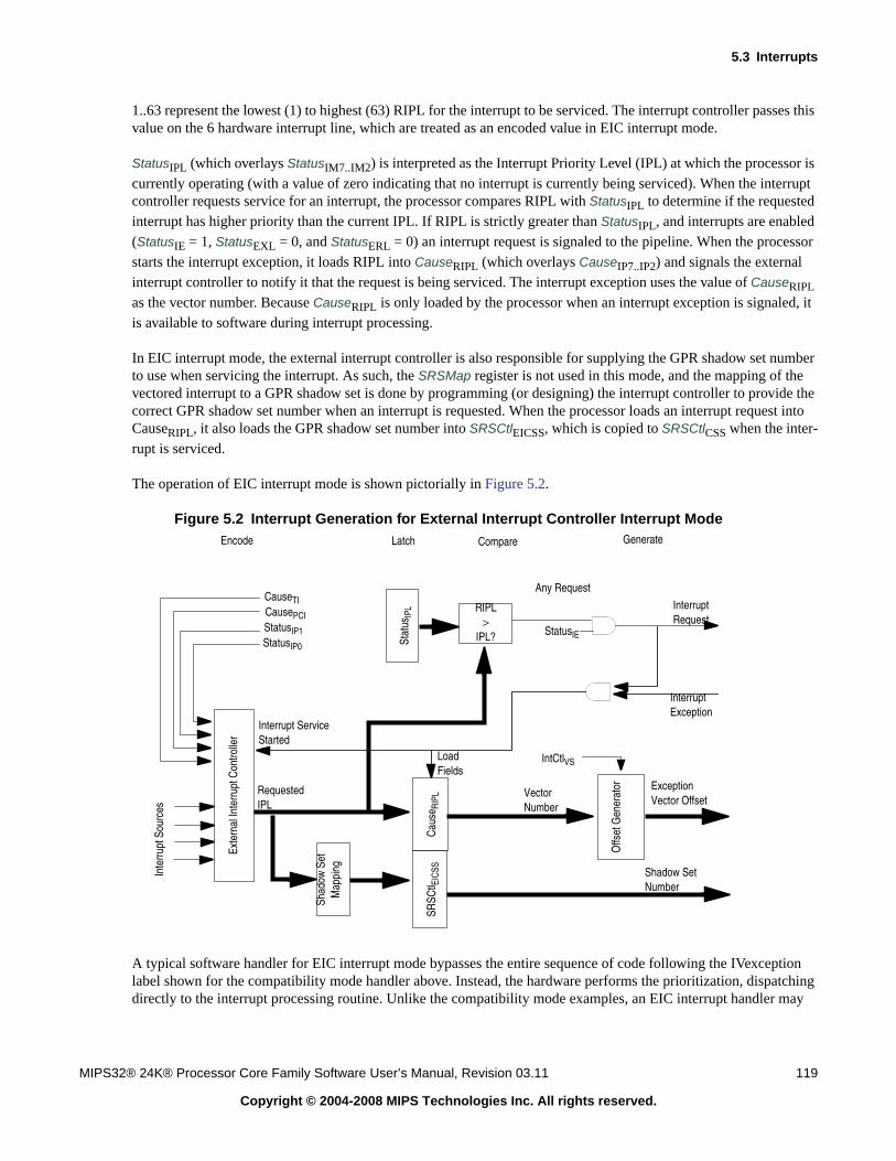
5.3 Interrupts
MIPS32® 24K® Processor Core Family Software User’s Manual, Revision 03.11 119
Copyright © 2004-2008 MIPS Technologies Inc. All rights reserved.
1..63 represent the lowest (1) to highest (63) RIPL for the interrupt to be serviced. The interrupt controller passes thisvalue on the 6 hardware interrupt line, which are treated as an encoded value in EIC interrupt mode.
StatusIPL (which overlays StatusIM7..IM2) is interpreted as the Interrupt Priority Level (IPL) at which the processor iscurrently operating (with a value of zero indicating that no interrupt is currently being serviced). When the interruptcontroller requests service for an interrupt, the processor compares RIPL with StatusIPL to determine if the requestedinterrupt has higher priority than the current IPL. If RIPL is strictly greater than StatusIPL, and interrupts are enabled(StatusIE = 1, StatusEXL = 0, and StatusERL = 0) an interrupt request is signaled to the pipeline. When the processorstarts the interrupt exception, it loads RIPL into CauseRIPL (which overlays CauseIP7..IP2) and signals the externalinterrupt controller to notify it that the request is being serviced. The interrupt exception uses the value of CauseRIPL
as the vector number. Because CauseRIPL is only loaded by the processor when an interrupt exception is signaled, itis available to software during interrupt processing.
In EIC interrupt mode, the external interrupt controller is also responsible for supplying the GPR shadow set numberto use when servicing the interrupt. As such, the SRSMap register is not used in this mode, and the mapping of thevectored interrupt to a GPR shadow set is done by programming (or designing) the interrupt controller to provide thecorrect GPR shadow set number when an interrupt is requested. When the processor loads an interrupt request intoCauseRIPL, it also loads the GPR shadow set number into SRSCtlEICSS, which is copied to SRSCtlCSS when the inter-rupt is serviced.
The operation of EIC interrupt mode is shown pictorially in Figure 5.2.
Figure 5.2 Interrupt Generation for External Interrupt Controller Interrupt Mode
A typical software handler for EIC interrupt mode bypasses the entire sequence of code following the IVexceptionlabel shown for the compatibility mode handler above. Instead, the hardware performs the prioritization, dispatchingdirectly to the interrupt processing routine. Unlike the compatibility mode examples, an EIC interrupt handler may
CauseTICausePCI
StatusIE
InterruptRequest
VectorNumber
Latch CompareEncode
Any Request
Offs
et G
ener
ator
IntCtlVS
ExceptionVector Offset
Generate
Shadow SetNumber
Exte
rnal
Inte
rrupt
Con
trolle
r
Inte
rrupt
Sou
rces
Shad
ow S
etM
appi
ng
StatusIP1StatusIP0
RequestedIPL
Cau
seR
IPL
Stat
usIP
L
SRSC
tl EIC
SS
RIPL>
IPL?
LoadFields
InterruptException
Interrupt ServiceStarted

Exceptions and Interrupts in the 24K® Core
120 MIPS32® 24K® Processor Core Family Software User’s Manual, Revision 03.11
Copyright © 2004-2008 MIPS Technologies Inc. All rights reserved.
take advantage of a dedicated GPR shadow set to avoid saving any registers. As such, the SimpleInterrupt code shownabove need not save the GPRs.
A nested interrupt is similar to that shown for compatibility mode, but may also take advantage of running the nestedexception routine in the GPR shadow set dedicated to the interrupt or in another shadow set. It also need only copyCauseRIPL to StatusIPL to prevent lower priority interrupts from interrupting the handler. Such a routine might lookas follows:
NestedException:/* * Nested exceptions typically require saving the EPC, Status,and SRSCtl registers, * setting up the appropriate GPR shadow set for the routine, disabling * the appropriate IM bits in Status to prevent an interrupt loop, putting * the processor in kernel mode, and re-enabling interrupts. The sample code * below can not cover all nuances of this processing and is intended only * to demonstrate the concepts. */
/* Use the current GPR shadow set, and setup software context */mfc0 k1, C0_Cause /* Read Cause to get RIPL value */mfc0 k0, C0_EPC /* Get restart address */srl k1, k1, S_CauseRIPL /* Right justify RIPL field */sw k0, EPCSave /* Save in memory */mfc0 k0, C0_Status /* Get Status value */sw k0, StatusSave /* Save in memory */ins k0, k1, S_StatusIPL, 6 /* Set IPL to RIPL in copy of Status */mfc0 k1, C0_SRSCtl /* Save SRSCtl if changing shadow sets */sw k1, SRSCtlSave/* If switching shadow sets, write new value to SRSCtlPSS here */ins k0, zero, S_StatusEXL, (W_StatusKSU+W_StatusERL+W_StatusEXL)
/* Clear KSU, ERL, EXL bits in k0 */mtc0 k0, C0_Status /* Modify IPL, switch to kernel mode, */
/* re-enable interrupts *//* * If switching shadow sets, clear only KSU above, write target * address to EPC, and do execute an eret to clear EXL, switch * shadow sets, and jump to routine */
/* Process interrupt here, including clearing device interrupt */
/* * The interrupt completion code is identical to that shown for VI mode above. */
5.3.2 Generation of Exception Vector Offsets for Vectored Interrupts
For vectored interrupts (in either VI or EIC interrupt mode), a vector number is produced by the interrupt controllogic. This number is combined with IntCtlVS to create the interrupt offset, which is added to 16#200 to create theexception vector offset. For VI interrupt mode, the vector number is in the range 0..7, inclusive. For EIC interruptmode, the vector number is in the range 1..63, inclusive (0 being the encoding for “no interrupt”). The IntCtlVS fieldspecifies the spacing between vector locations. If this value is zero (the default reset state), the vector spacing is zero

5.4 GPR Shadow Registers
MIPS32® 24K® Processor Core Family Software User’s Manual, Revision 03.11 121
Copyright © 2004-2008 MIPS Technologies Inc. All rights reserved.
and the processor reverts to Interrupt Compatibility Mode. A non-zero value enables vectored interrupts, and Table5.4 shows the exception vector offset for a representative subset of the vector numbers and values of the IntCtlVS field.
The general equation for the exception vector offset for a vectored interrupt is:
vectorOffset ← 16#200 + (vectorNumber × (IntCtlVS || 2#00000))
5.4 GPR Shadow Registers
Release 2 of the Architecture optionally removes the need to save and restore GPRs on entry to high priority inter-rupts or exceptions, and to provide specified processor modes with the same capability. This is done by introducingmultiple copies of the GPRs, called shadow sets, and allowing privileged software to associate a shadow set withentry to kernel mode via an interrupt vector or exception. The normal GPRs are logically considered shadow set zero.
The number of GPR shadow sets is a build-time option on the 24K core. Although Release 2 of the Architecturedefines a maximum of 16 shadow sets, the core allows one (the normal GPRs), two, or four shadow sets. The highestnumber actually implemented is indicated by the SRSCtlHSS field. If this field is zero, only the normal GPRs areimplemented.
Shadow sets are new copies of the GPRs that can be substituted for the normal GPRs on entry to kernel mode via aninterrupt or exception. Once a shadow set is bound to a kernel mode entry condition, reference to GPRs work exactlyas one would expect, but they are redirected to registers that are dedicated to that condition. Privileged software mayneed to reference all GPRs in the register file, even specific shadow registers that are not visible in the current mode.The RDPGPR and WRPGPR instructions are used for this purpose. The CSS field of the SRSCtl register provides thenumber of the current shadow register set, and the PSS field of the SRSCtl register provides the number of the previ-ous shadow register set (that which was current before the last exception or interrupt occurred).
If the processor is operating in VI interrupt mode, binding of a vectored interrupt to a shadow set is done by writing tothe SRSMap register. If the processor is operating in EIC interrupt mode, the binding of the interrupt to a specific
Table 5.4 Exception Vector Offsets for Vectored Interrupts
Vector Number
Value of IntCtlVS Field
2#00001 2#00010 2#00100 2#01000 2#10000
0 16#0200 16#0200 16#0200 16#0200 16#0200
1 16#0220 16#0240 16#0280 16#0300 16#0400
2 16#0240 16#0280 16#0300 16#0400 16#0600
3 16#0260 16#02C0 16#0380 16#0500 16#0800
4 16#0280 16#0300 16#0400 16#0600 16#0A00
5 16#02A0 16#0340 16#0480 16#0700 16#0C00
6 16#02C0 16#0380 16#0500 16#0800 16#0E00
7 16#02E0 16#03C0 16#0580 16#0900 16#1000
•••
61 16#09A0 16#1140 16#2080 16#3F00 16#7C00
62 16#09C0 16#1180 16#2100 16#4000 16#7E00
63 16#09E0 16#11C0 16#2180 16#4100 16#8000

Exceptions and Interrupts in the 24K® Core
122 MIPS32® 24K® Processor Core Family Software User’s Manual, Revision 03.11
Copyright © 2004-2008 MIPS Technologies Inc. All rights reserved.
shadow set is provided by the external interrupt controller, and is configured in an implementation-dependent way.Binding of an exception or non-vectored interrupt to a shadow set is done by writing to the ESS field of the SRSCtlregister. When an exception or interrupt occurs, the value of SRSCtlCSS is copied to SRSCtlPSS, and SRSCtlCSS is setto the value taken from the appropriate source. On an ERET, the value of SRSCtlPSS is copied back into SRSCtlCSS torestore the shadow set of the mode to which control returns. More precisely, the rules for updating the fields in theSRSCtl register on an interrupt or exception are as follows:
1. No field in the SRSCtl register is updated if any of the following conditions is true. In this case, steps 2 and 3 areskipped.
• The exception is one that sets StatusERL: Reset or NMI.
• The exception causes entry into EJTAG Debug Mode
• StatusBEV = 1
• StatusEXL = 1
2. SRSCtlCSS is copied to SRSCtlPSS
3. SRSCtlCSS is updated from one of the following sources:
• The appropriate field of the SRSMap register, based on IPL, if the exception is an interrupt, CauseIV = 1,Config3VEIC = 0, and Config3VInt = 1. These are the conditions for a vectored interrupt.
• The EICSS field of the SRSCtl register if the exception is an interrupt, CauseIV = 1, and Config3VEIC = 1.These are the conditions for a vectored EIC interrupt.
• The ESS field of the SRSCtl register in any other case. This is the condition for a non-interrupt exception, ora non-vectored interrupt.
Similarly, the rules for updating the fields in the SRSCtl register at the end of an exception or interrupt are as follows:
1. No field in the SRSCtl register is updated if any of the following conditions is true. In this case, step 2 is skipped.
• A DERET is executed
• An ERET is executed with StatusERL = 1
2. SRSCtlPSS is copied to SRSCtlCSS
These rules have the effect of preserving the SRSCtl register in any case of a nested exception or one which occursbefore the processor has been fully initialized (StatusBEV = 1).
Privileged software may switch the current shadow set by writing a new value into SRSCtlPSS, loading EPC with atarget address, and doing an ERET.

5.5 Exception Vector Locations
MIPS32® 24K® Processor Core Family Software User’s Manual, Revision 03.11 123
Copyright © 2004-2008 MIPS Technologies Inc. All rights reserved.
5.5 Exception Vector Locations
The Reset, Soft Reset, NMI and EJTAG Debug exceptions are vectored to a specific location as shown in Table 5.5and Table 5.6. Addresses for all other exceptions are a combination of a vector offset and a vector base address. InRelease 1 of the architecture, the vector base address was fixed. In Release 2 of the architecture, software is allowedto specify the vector base address via the EBase register for exceptions that occur when StatusBEV equals 0. Anotherdegree of flexibility in the selection of the vector base address, for use when StatusBEV equals 1, is provided via a setof input pins, SI_UseExceptionBase and SI_ExceptionBase[29:12]. Table 5.5 gives the vector base address whenSI_UseExceptionBase equals 0, as a function of the exception and whether the BEV bit is set in the Status register.Table 5.6 gives the vector base addresses when SI_UseExceptionBase equals 1. As can be seen in Table 5.6, whenSI_UseExceptionBase equals 1, the exception vectors for cases where StatusBEV equals 0 are not affected.
Table 5.7 gives the offsets from the vector base address as a function of the exception. Note that the IV bit in theCause register causes Interrupts to use a dedicated exception vector offset, rather than the general exception vector.Table 5.4 gives the offset from the base address in the case where StatusBEV = 0 and CauseIV = 1. Table 5.8 com-bines these two tables into one that contains all possible vector addresses as a function of the state that can affect thevector selection. To avoid complexity in the table, it is assumed that IntCtlVS is 0.
Table 5.6 Exception Vector Base Addresses when SI_UseExceptionBase equals 1
Table 5.5 Exception Vector Base Addresses when SI_UseExceptionBase equals 0
Exception
StatusBEV
0 1
Reset, NMI 16#BFC0.0000
EJTAG Debug (with ProbEn = 0 inthe EJTAG_Control_register)
16#BFC0.0480
EJTAG Debug (with ProbEn = 1 inthe EJTAG_Control_register)
16#FF20.0200
Cache Error EBase31..30 || 1 ||EBase28..12 || 16#000
Note that EBase31..30 have the fixed
value 2#10
16#BFC0.0300
Other EBase31..12 || 16#000Note that EBase31..30 have the fixed
value 2#10
16#BFC0.0200
‘||’ denotes bit string concatenation
Exception
StatusBEV
0 1
Reset, NMI 2#10 || SI_ExceptionBase[29:12] || 16#000
EJTAG Debug (with ProbEn =0in the EJTAG_Control_register)
2#10 ||SI_ExceptionBase[29:12] || 16#480

Exceptions and Interrupts in the 24K® Core
124 MIPS32® 24K® Processor Core Family Software User’s Manual, Revision 03.11
Copyright © 2004-2008 MIPS Technologies Inc. All rights reserved.
EJTAG Debug (with ProbEn =1in the EJTAG_Control_register)
16#FF20.0200
Cache Error EBase31..30 || 1 ||EBase28..12 || 16#000
Note that EBase31..30 have the fixed
value 2#10
2#101 || SI_ExceptionBase[28:12] || 16#300
Other EBase31..12 || 16#000Note that EBase31..30 have the fixed
value 2#10
2#10 || SI_ExceptionBase[29:12] || 16#200
‘||’ denotes bit string concatenation
Table 5.7 Exception Vector Offsets
Exception Vector Offset
TLB Refill, EXL = 0 16#000
General Exception 16#180
Interrupt, CauseIV = 1 16#200 (this is the base of the vectored inter-rupt table when StatusBEV = 0)
Reset, NMI None (Uses Reset Base Address)
Table 5.8 Exception Vectors
Exception SI_
Use
Exc
epti
on
Bas
e
Sta
tus B
EV
Sta
tus E
XL
Cau
seIV
EJT
AG
Pro
bE
n
Vector
Assumes that IntCtlVS = 0
Reset, NMI 0 x x x x 16#BFC0.0000
Reset, NMI 1 x x x x 2#10 || SI_ExceptionBase[29:12] || 16#000
EJTAGDebug
0 x x x 0 16#BFC0.0480
EJTAGDebug
1 x x x 0 2#10 || SI_ExceptionBase[29:12] || 16#480
EJTAGDebug
x x x x 1 16#FF20.0200
TLB Refill 0 0 1 x x 16#EBase[31:12] || 16#180
TLB Refill 0 1 0 x x 16#BFC0.0200
TLB Refill 1 1 0 x x 2#10 || SI_ExceptionBase[29:12] || 16#200
TLB Refill 0 1 1 x x 16#BFC0.0380
Exception
StatusBEV
0 1

5.6 General Exception Processing
MIPS32® 24K® Processor Core Family Software User’s Manual, Revision 03.11 125
Copyright © 2004-2008 MIPS Technologies Inc. All rights reserved.
5.6 General Exception Processing
With the exception of Reset, NMI, cache error, and EJTAG Debug exceptions, which have their own special process-ing as described below, exceptions have the same basic processing flow:
• If the EXL bit in the Status register is zero, the EPC register is loaded with the PC at which execution will berestarted and the BD bit is set appropriately in the Cause register (see Table 6.24). The value loaded into the EPCregister is dependent on whether the processor implements the MIPS16 ASE, and whether the instruction is inthe delay slot of a branch or jump which has delay slots. Table 5.9 shows the value stored in each of the CP0 PCregisters, including EPC. For implementations of Release 2 of the Architecture if StatusBEV = 0, the CSS field inthe SRSCtl register is copied to the PSS field, and the CSS value is loaded from the appropriate source.
If the EXL bit in the Status register is set, the EPC register is not loaded and the BD bit is not changed in theCause register. For implementations of Release 2 of the Architecture, the SRSCtl register is not changed.
TLB Refill 1 1 1 x x 2#10 || SI_ExceptionBase[29:12] || 16#380
Cache Error 0 0 x x x 16#EBase[31:30] || 2#1 || EBase[28:12] || 16#100
Cache Error 0 1 x x x 16#BFC0.0300
Cache Error 1 1 x x x 2#101 || SI_ExceptionBase[28:12] || 16#300
Interrupt x 0 0 0 x 16#EBase[31:12] || 16#180
Interrupt x 0 0 1 x 16#EBase[31:12] || 16#200
Interrupt 0 1 0 0 x 16#BFC0.0380
Interrupt 1 1 0 0 x 2#10 || SI_ExceptionBase[29:12] || 16#380
Interrupt 0 1 0 1 x 16#BFC0.0400
Interrupt 1 1 0 1 x 2#10 || SI_ExceptionBase[29:12] || 16#400
All others 0 0 x x x 16#EBase[31:12] || 16#180
All others 0 1 x x x 16#BFC0.0380
All others 1 1 x x x 2#10 || SI_ExceptionBase[29:12] || 16#380
‘x’ denotes don’t care, ‘||’ denotes bit string concatenation
Table 5.9 Value Stored in EPC, ErrorEPC, or DEPC on an Exception
MIPS16Implemented?
In Branch/JumpDelay Slot? Value stored in EPC/ErrorEPC/DEPC
No No Address of the instruction
No Yes Address of the branch or jump instruction (PC-4)
Table 5.8 Exception Vectors (Continued)
Exception SI_
Use
Exc
epti
on
Bas
e
Sta
tus B
EV
Sta
tus E
XL
Cau
seIV
EJT
AG
Pro
bE
n
Vector
Assumes that IntCtlVS = 0

Exceptions and Interrupts in the 24K® Core
126 MIPS32® 24K® Processor Core Family Software User’s Manual, Revision 03.11
Copyright © 2004-2008 MIPS Technologies Inc. All rights reserved.
• The CE, and ExcCode fields of the Cause registers are loaded with the values appropriate to the exception. TheCE field is loaded, but not defined, for any exception type other than a coprocessor unusable exception.
• The EXL bit is set in the Status register.
• The processor is started at the exception vector.
The value loaded into EPC represents the restart address for the exception and need not be modified by exceptionhandler software in the normal case. Software need not look at the BD bit in the Cause register unless it wishes toidentify the address of the instruction that actually caused the exception.
Note that individual exception types may load additional information into other registers. This is noted in the descrip-tion of each exception type below.
Operation:
/* If StatusEXL is 1, all exceptions go through the general exception vector *//* and neither EPC nor CauseBD nor SRSCtl are modified */if StatusEXL = 1 then
vectorOffset ← 16#180else
/* For implementations that include the MIPS16e ASE, calculate potential *//* PC adjustment for exceptions in the delay slot */if Config1CA = 0 then
restartPC ← PCbranchAdjust ← 4 /* Possible adjustment for delay slot */
elserestartPC ← PC31..1 || ISAModeif (ISAMode = 0) or ExtendedMIPS16Instruction
branchAdjust ← 4 /* Possible adjustment for 32-bit MIPS delay slot */else
branchAdjust ← 2 /* Possible adjustment for MIPS16 delay slot */endif
endifif InstructionInBranchDelaySlot then
EPC ← restartPC - branchAdjust/* PC of branch/jump */CauseBD ← 1
elseEPC ← restartPC /* PC of instruction */CauseBD ← 0
endif
/* Compute vector offsets as a function of the type of exception */NewShadowSet ← SRSCtlESS /* Assume exception, Release 2 only */if ExceptionType = TLBRefill then
vectorOffset ← 16#000
Yes No Upper 31 bits of the address of the instruction, combinedwith the ISA Mode bit
Yes Yes Upper 31 bits of the branch or jump instruction (PC-2 inthe MIPS16 ISA Mode and PC-4 in the 32-bit ISA Mode),combined with the ISA Mode bit
Table 5.9 Value Stored in EPC, ErrorEPC, or DEPC on an Exception
MIPS16Implemented?
In Branch/JumpDelay Slot? Value stored in EPC/ErrorEPC/DEPC

5.7 Debug Exception Processing
MIPS32® 24K® Processor Core Family Software User’s Manual, Revision 03.11 127
Copyright © 2004-2008 MIPS Technologies Inc. All rights reserved.
elseif (ExceptionType = Interrupt) thenif (CauseIV = 0) then
vectorOffset ← 16#180else
if (StatusBEV = 1) or (IntCtlVS = 0) thenvectorOffset ← 16#200
elseif Config3VEIC = 1 then
VecNum ← CauseRIPLNewShadowSet ← SRSCtlEICSS
elseVecNum ← VIntPriorityEncoder()NewShadowSet ← SRSMapIPL×4+3..IPL×4
endifvectorOffset ← 16#200 + (VecNum × (IntCtlVS || 2#00000))
endif /* if (StatusBEV = 1) or (IntCtlVS = 0) then */endif /* if (CauseIV = 0) then */
endif /* elseif (ExceptionType = Interrupt) then */
/* Update the shadow set information for an implementation of *//* Release 2 of the architecture */if ((ArchitectureRevision ≥ 2) and (SRSCtlHSS > 0) and (StatusBEV = 0) and
(StatusERL = 0)) thenSRSCtlPSS ← SRSCtlCSSSRSCtlCSS ← NewShadowSet
endifendif /* if StatusEXL = 1 then */
CauseCE ← FaultingCoprocessorNumberCauseExcCode ← ExceptionTypeStatusEXL ← 1
if Config1CA = 1 thenISAMode ← 0
endif
/* Calculate the vector base address */if StatusBEV = 1 then
vectorBase ← 16#BFC0.0200else
if ArchitectureRevision ≥ 2 then/* The fixed value of EBase31..30 forces the base to be in kseg0 or kseg1 */vectorBase ← EBase31..12 || 16#000
elsevectorBase ← 16#8000.0000
endifendif
/* Exception PC is the sum of vectorBase and vectorOffset */PC ← vectorBase31..30 || (vectorBase29..0 + vectorOffset29..0)
/* No carry between bits 29 and 30 */
5.7 Debug Exception Processing
All debug exceptions have the same basic processing flow:

Exceptions and Interrupts in the 24K® Core
128 MIPS32® 24K® Processor Core Family Software User’s Manual, Revision 03.11
Copyright © 2004-2008 MIPS Technologies Inc. All rights reserved.
• The DEPC register is loaded with the program counter (PC) value at which execution will be restarted and theDBD bit is set appropriately in the Debug register. The value loaded into the DEPC register is the current PC ifthe instruction is not in the delay slot of a branch, or the PC-4 of the branch if the instruction is in the delay slotof a branch.
• The DSS, DBp, DDBL, DDBS, DIB and DINT bits (D* bits at [5:0]) in the Debug register are updated appropri-ately depending on the debug exception type.
• Halt and Doze bits in the Debug register are updated appropriately.
• DM bit in the Debug register is set to 1.
• The processor is started at the debug exception vector.
The value loaded into DEPC represents the restart address for the debug exception and need not be modified by thedebug exception handler software in the usual case. Debug software need not look at the DBD bit in the Debug regis-ter unless it wishes to identify the address of the instruction that actually caused the debug exception.
A unique debug exception is indicated through the DSS, DBp, DDBL, DDBS, DIB and DINT bits (D* bits at [5:0])in the Debug register.
No other CP0 registers or fields are changed due to the debug exception, thus no additional state is saved.
Operation:
if InstructionInBranchDelaySlot thenDEPC ← PC-4DebugDBD ← 1
elseDEPC ← PCDebugDBD ← 0
endifDebugD* bits at at [5:0] ← DebugExceptionTypeDebugHalt ← HaltStatusAtDebugExceptionDebugDoze ← DozeStatusAtDebugExceptionDebugDM ← 1if EJTAGControlRegisterProbTrap = 1 then
PC ← 0xFF20_0200else
PC ← 0xBFC0_0480endif
The same debug exception vector location is used for all debug exceptions. The location is determined by the Prob-Trap bit in the EJTAG Control register (ECR), as shown in Table 5.10.
Table 5.10 Debug Exception Vector Addresses
ProbTrap bit inECR Register Debug Exception Vector Address
0 0xBFC0_0480
1 0xFF20_0200 in dmseg

5.8 Exceptions
MIPS32® 24K® Processor Core Family Software User’s Manual, Revision 03.11 129
Copyright © 2004-2008 MIPS Technologies Inc. All rights reserved.
5.8 Exceptions
The following subsections describe each of the exceptions listed in the same sequence as shown in Table 5.1.
5.8.1 Reset Exception
A reset exception occurs when the SI_Reset signal is asserted to the processor. This exception is not maskable. Whena Reset exception occurs, the processor performs a full reset initialization, including aborting state machines, estab-lishing critical state, and generally placing the processor in a state in which it can execute instructions from uncached,unmapped address space. On a Reset exception, the state of the processor is not defined, with the following excep-tions:
• The Random register is initialized to the number of TLB entries - 1.
• The Wired register is initialized to zero.
• The Config register is initialized with its boot state.
• The RP, BEV, TS, SR, NMI, and ERL fields of the Status register are initialized to a specified state.
• The I, R, and W fields of the WatchLo register are initialized to 0.
• The ErrorEPC register is loaded with PC-4 if the state of the processor indicates that it was executing an instruc-tion in the delay slot of a branch. Otherwise, the ErrorEPC register is loaded with PC. Note that this value may ormay not be predictable.
• PC is loaded with 0xBFC0_0000.
Cause Register ExcCode Value:
None
Additional State Saved:
None
Entry Vector Used:
Reset (0xBFC0_0000)
Operation:
Random ← TLBEntries - 1Wired ← 0Config ← ConfigurationStateStatusRP ← 0StatusBEV ← 1StatusTS ← 0StatusSR ← 0StatusNMI ← 0StatusERL ← 1WatchLoI ← 0WatchLoR ← 0WatchLoW ← 0if InstructionInBranchDelaySlot then
ErrorEPC ← PC - 4

Exceptions and Interrupts in the 24K® Core
130 MIPS32® 24K® Processor Core Family Software User’s Manual, Revision 03.11
Copyright © 2004-2008 MIPS Technologies Inc. All rights reserved.
elseErrorEPC ← PC
endifPC ← 0xBFC0_0000
5.8.2 Debug Single Step Exception
A debug single step exception occurs after the CPU has executed one/two instructions in non-debug mode, whenreturning to non-debug mode after debug mode. One instruction is allowed to execute when returning to an instruc-tion without a delay slot, otherwise two instructions are allowed to execute since the jump/branch and the instructionin the delay slot are executed as one step. Debug single step exceptions are enabled by the SSt bit in the Debug regis-ter, and are always disabled for the first one/two instructions after a DERET.
The DEPC register points to the instruction on which the debug single step exception occurred, which is also the nextinstruction to single step or execute when returning from debug mode. So the DEPC will not point to the instructionwhich has just been single stepped, but rather the following instruction. The DBD bit in the Debug register is neverset for a debug single step exception, since the jump/branch and the instruction in the delay slot is executed in onestep.
Exceptions occurring on the instruction(s) executed with debug single step exception enabled are taken even thoughdebug single step was enabled. For a normal exception (other than reset), a debug single step exception is then takenon the first instruction in the normal exception handler. Debug exceptions are unaffected by single step mode, e.g.returning to a SDBBP instruction with debug single step exceptions enabled causes a debug software breakpointexception, and the DEPC will point to the SDBBP instruction. However, returning to an instruction (not jump/branch)just before the SDBBP instruction, causes a debug single step exception with the DEPC pointing to the SDBBPinstruction.
To ensure proper functionality of single step, the debug single step exception has priority over all other exceptions,except reset and soft reset.
Debug Register Debug Status Bit Set
DSS
Additional State Saved
None
Entry Vector Used
Debug exception vector
5.8.3 Debug Interrupt Exception
A debug interrupt exception is either caused by the EjtagBrk bit in the EJTAG Control register (controlled through theTAP), or caused by the debug interrupt request signal to the CPU.
The debug interrupt exception is an asynchronous debug exception which is taken as soon as possible, but with nospecific relation to the executed instructions. The DEPC register is set to the instruction where execution should con-tinue after the debug handler is through. The DBD bit is set based on whether the interrupted instruction was execut-ing in the delay slot of a branch.
Debug Register Debug Status Bit Set
DINT

5.8 Exceptions
MIPS32® 24K® Processor Core Family Software User’s Manual, Revision 03.11 131
Copyright © 2004-2008 MIPS Technologies Inc. All rights reserved.
Additional State Saved
None
Entry Vector Used
Debug exception vector
5.8.4 Non-Maskable Interrupt (NMI) Exception
A non maskable interrupt exception occurs when the SI_NMI signal is asserted to the processor. SI_NMI is an edgesensitive signal - only one NMI exception will be taken each time it is asserted. An NMI exception occurs only atinstruction boundaries, so it does not cause any reset or other hardware initialization. The state of the cache, memory,and other processor states are consistent and all registers are preserved, with the following exceptions:
• The BEV, TS, SR, NMI, and ERL fields of the Status register are initialized to a specified state.
• The ErrorEPC register is loaded with PC-4 if the state of the processor indicates that it was executing an instruc-tion in the delay slot of a branch. Otherwise, the ErrorEPC register is loaded with PC.
• PC is loaded with 0xBFC0_0000.
Cause Register ExcCode Value:
None
Additional State Saved:
None
Entry Vector Used:
Reset (0xBFC0_0000)
Operation:
StatusBEV ← 1StatusTS ← 0StatusSR ← 0StatusNMI ← 1StatusERL ← 1if InstructionInBranchDelaySlot then
ErrorEPC ← PC - 4else
ErrorEPC ← PCendifPC ← 0xBFC0_0000
5.8.5 Machine Check Exception
A machine check exception occurs when the processor detects an internal inconsistency. The following conditioncauses a machine check exception:
• The detection of multiple matching entries in the TLB. The core detects this condition on a TLB write and pre-vents the write from being completed. The TS bit in the Status register is set to indicate this condition. This bit isonly a status flag and does not affect the operation of the device. Software clears this bit at the appropriate time.This condition is resolved by flushing the conflicting TLB entries. The TLB write can then be completed.

Exceptions and Interrupts in the 24K® Core
132 MIPS32® 24K® Processor Core Family Software User’s Manual, Revision 03.11
Copyright © 2004-2008 MIPS Technologies Inc. All rights reserved.
Cause Register ExcCode Value:
MCheck
Additional State Saved:
None
Entry Vector Used:
General exception vector (offset 0x180)
5.8.6 Interrupt Exception
The interrupt exception occurs when one or more of the six hardware, two software, or timer interrupt requests isenabled by the Status register and the interrupt input is asserted. See Section 5.3 “Interrupts” for more details aboutthe processing of interrupts.
Register ExcCode Value:
Int
Additional State Saved:
Entry Vector Used:
See Section 5.3.2 “Generation of Exception Vector Offsets for Vectored Interrupts” for the entry vector used,depending on the interrupt mode the processor is operating in.
5.8.7 Debug Instruction Break Exception
A debug instruction break exception occurs when an instruction hardware breakpoint matches an executed instruc-tion. The DEPC register and DBD bit in the Debug register indicate the instruction that caused the instruction hard-ware breakpoint to match. This exception can only occur if instruction hardware breakpoints are implemented.
Debug Register Debug Status Bit Set:
DIB
Additional State Saved:
None
Entry Vector Used:
Debug exception vector
5.8.8 Watch Exception — Instruction Fetch or Data Access
The Watch facility provides a software debugging vehicle by initiating a watch exception when an instruction or datareference matches the address information stored in the WatchHi and WatchLo registers. A Watch exception is takenimmediately if the EXL and ERL bits of the Status register are both zero and the DM bit of the Debug is also zero. If
Table 5.11 Register States an Interrupt Exception
Register State Value
CauseIP indicates the interrupts that are pending.

5.8 Exceptions
MIPS32® 24K® Processor Core Family Software User’s Manual, Revision 03.11 133
Copyright © 2004-2008 MIPS Technologies Inc. All rights reserved.
any of those bits is a one at the time that a watch exception would normally be taken, then the WP bit in the Causeregister is set, and the exception is deferred until all three bits are zero. Software may use the WP bit in the Cause reg-ister to determine if the EPC register points at the instruction that caused the watch exception, or if the exceptionactually occurred while in kernel mode.
The Watch exception can occur on either an instruction fetch or a data access. Watch exceptions that occur on aninstruction fetch have a higher priority than watch exceptions that occur on a data access.
Register ExcCode Value:
WATCH
Additional State Saved:
Entry Vector Used:
General exception vector (offset 0x180)
5.8.9 Address Error Exception — Instruction Fetch/Data Access
An address error exception occurs on an instruction or data access when an attempt is made to execute one of the fol-lowing:
• Fetch an instruction, load a word, or store a word that is not aligned on a word boundary
• Load or store a halfword that is not aligned on a halfword boundary
• Reference the kernel address space from user mode
Note that in the case of an instruction fetch that is not aligned on a word boundary, PC is updated before the conditionis detected. Therefore, both EPC and BadVAddr point to the unaligned instruction address. In the case of a data accessthe exception is taken if either an unaligned address or an address that was inaccessible in the current processor modewas referenced by a load or store instruction.
Cause Register ExcCode Value:
ADEL: Reference was a load or an instruction fetch
ADES: Reference was a store
Table 5.12 Register States on a Watch Exception
Register State Value
CauseWP Indicates that the watch exception was deferred until afterStatusEXL, StatusERL, and DebugDM were zero. This bit
directly causes a watch exception, so software must clearthis bit as part of the exception handler to prevent a watchexception loop at the end of the current handler execution.
WatchHiI,R,W Set for the watch channel that matched, and indicateswhich type of match there was.
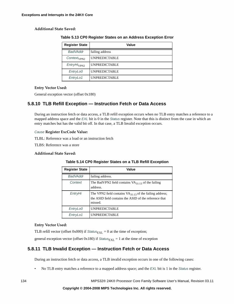
Exceptions and Interrupts in the 24K® Core
134 MIPS32® 24K® Processor Core Family Software User’s Manual, Revision 03.11
Copyright © 2004-2008 MIPS Technologies Inc. All rights reserved.
Additional State Saved:
Entry Vector Used:
General exception vector (offset 0x180)
5.8.10 TLB Refill Exception — Instruction Fetch or Data Access
During an instruction fetch or data access, a TLB refill exception occurs when no TLB entry matches a reference to amapped address space and the EXL bit is 0 in the Status register. Note that this is distinct from the case in which anentry matches but has the valid bit off. In that case, a TLB Invalid exception occurs.
Cause Register ExcCode Value:
TLBL: Reference was a load or an instruction fetch
TLBS: Reference was a store
Additional State Saved:
Entry Vector Used:
TLB refill vector (offset 0x000) if StatusEXL = 0 at the time of exception;
general exception vector (offset 0x180) if StatusEXL = 1 at the time of exception
5.8.11 TLB Invalid Exception — Instruction Fetch or Data Access
During an instruction fetch or data access, a TLB invalid exception occurs in one of the following cases:
• No TLB entry matches a reference to a mapped address space; and the EXL bit is 1 in the Status register.
Table 5.13 CP0 Register States on an Address Exception Error
Register State Value
BadVAddr failing address
ContextVPN2 UNPREDICTABLE
EntryHiVPN2 UNPREDICTABLE
EntryLo0 UNPREDICTABLE
EntryLo1 UNPREDICTABLE
Table 5.14 CP0 Register States on a TLB Refill Exception
Register State Value
BadVAddr failing address.
Context The BadVPN2 field contains VA31:13 of the failing
address.
EntryHi The VPN2 field contains VA31:13 of the failing address;
the ASID field contains the ASID of the reference thatmissed.
EntryLo0 UNPREDICTABLE
EntryLo1 UNPREDICTABLE

5.8 Exceptions
MIPS32® 24K® Processor Core Family Software User’s Manual, Revision 03.11 135
Copyright © 2004-2008 MIPS Technologies Inc. All rights reserved.
• A TLB entry matches a reference to a mapped address space, but the matched entry has the valid bit off.
Cause Register ExcCode Value:
TLBL: Reference was a load or an instruction fetch
TLBS: Reference was a store
Additional State Saved:
Entry Vector Used:
General exception vector (offset 0x180)
5.8.12 Cache Error Exception
A cache error exception occurs when an instruction or data reference detects a cache tag or data error. This exceptionis not maskable. To avoid disturbing the error in the cache array the exception vector is to an unmapped, uncachedaddress. This exception can be imprecise and the ErrorEPC may not point to the instruction that saw the errorL2cache errors are considered to be imprecise. An L2 cache error on a data load operation can potentially corrupt thetarget GPR.
Cause Register ExcCode Value
N/A
Additional State Saved
Entry Vector Used
Cache error vector (offset 16#100)
5.8.13 Bus Error Exception — Instruction Fetch or Data Access
A bus error exception occurs when an instruction or data access makes a bus request (due to a cache miss or anuncacheable reference) and that request terminates in an error. The bus error exception can occur on either an instruc-
Table 5.15 CP0 Register States on a TLB Invalid Exception
Register State Value
BadVAddr failing address
Context The BadVPN2 field contains VA31:13 of the failing
address.
EntryHi The VPN2 field contains VA31:13 of the failing address;
the ASID field contains the ASID of the reference thatmissed.
EntryLo0 UNPREDICTABLE
EntryLo1 UNPREDICTABLE
Table 5.16 CP0 Register States on a Cache Error Exception
Register State Value
CacheErr Error state
ErrorEPC Restart PC

Exceptions and Interrupts in the 24K® Core
136 MIPS32® 24K® Processor Core Family Software User’s Manual, Revision 03.11
Copyright © 2004-2008 MIPS Technologies Inc. All rights reserved.
tion fetch or a data read. Bus error exceptions cannot be generated on data writes. Bus error exceptions that occur onan instruction fetch have a higher priority than bus error exceptions that occur on a data access.
Bus Error exceptions on instruction fetch (IBE) are precise. Bus errors on data load operations (DBE) are consideredto be imprecise. These errors are taken when the ERR code is returned on the OC_SResp input. Bus errors on dataload operations can potentially corrupt the target GPR.
Cause Register ExcCode Value:
IBE: Error on an instruction reference
DBE: Error on a data reference
Additional State Saved:
None
Entry Vector Used:
General exception vector (offset 0x180)
5.8.14 Debug Software Breakpoint Exception
A debug software breakpoint exception occurs when an SDBBP instruction is executed. The DEPC register and DBDbit in the Debug register will indicate the SDBBP instruction that caused the debug exception.
Debug Register Debug Status Bit Set:
DBp
Additional State Saved:
None
Entry Vector Used:
Debug exception vector
5.8.15 Execution Exception — System Call
The system call exception is one of the execution exceptions. All of these exceptions have the same priority. A sys-tem call exception occurs when a SYSCALL instruction is executed.
Cause Register ExcCode Value:
Sys
Additional State Saved:
None
Entry Vector Used:
General exception vector (offset 0x180)
5.8.16 Execution Exception — Breakpoint
The breakpoint exception is one of the execution exceptions. All of these exceptions have the same priority. A break-point exception occurs when a BREAK instruction is executed.

5.8 Exceptions
MIPS32® 24K® Processor Core Family Software User’s Manual, Revision 03.11 137
Copyright © 2004-2008 MIPS Technologies Inc. All rights reserved.
Cause Register ExcCode Value:
Bp
Additional State Saved:
None
Entry Vector Used:
General exception vector (offset 0x180)
5.8.17 Execution Exception — Reserved Instruction
The reserved instruction exception is one of the execution exceptions. All of these exceptions have the same priority.A reserved instruction exception occurs when a reserved or undefined major opcode or function field is executed.This includes Coprocessor 2 instructions which are decoded reserved in the Coprocessor 2.
Cause Register ExcCode Value:
RI
Additional State Saved:
None
Entry Vector Used:
General exception vector (offset 0x180)
5.8.18 Execution Exception — Coprocessor Unusable
The coprocessor unusable exception is one of the execution exceptions. All of these exceptions have the same prior-ity. A coprocessor unusable exception occurs when an attempt is made to execute a coprocessor instruction for one ofthe following:
• a corresponding coprocessor unit that has not been marked usable by setting its CU bit in the Status register
• CP0 instructions, when the unit has not been marked usable, and the processor is executing in user mode
Cause Register ExcCode Value:
CpU
Additional State Saved:
Entry Vector Used:
General exception vector (offset 0x180)
Table 5.17 Register States on a Coprocessor Unusable Exception
Register State Value
CauseCE unit number of the coprocessor being referenced

Exceptions and Interrupts in the 24K® Core
138 MIPS32® 24K® Processor Core Family Software User’s Manual, Revision 03.11
Copyright © 2004-2008 MIPS Technologies Inc. All rights reserved.
5.8.19 Execution Exception — CorExtend block Unusable
The CorExtend block unusable exception is one of the execution exceptions. All of these exceptions have the samepriority. A CEU exception occurs when an attempt is made to execute a CorExtend instruction when the CEE bit inthe Status register is not set. It is dependent on the implementation of the CorExtend block, but this exception shouldbe taken on any CorExtend instruction that modifies local state within the CorExtend block and can optionally betaken on other CorExtend instructions.
Cause Register ExcCode Value:
CEU
Additional State Saved:
None
Entry Vector Used:
General exception vector (offset 0x180)
5.8.20 Execution Exception — Floating Point Exception
A floating point exception is initiated by the floating point coprocessor.
Cause Register ExcCode Value:
FPE
Additional State Saved:
Entry Vector Used:
General exception vector (offset 0x180)
5.8.21 Execution Exception — Integer Overflow
The integer overflow exception is one of the execution exceptions. All of these exceptions have the same priority. Aninteger overflow exception occurs when selected integer instructions result in a 2’s complement overflow.
Cause Register ExcCode Value:
Ov
Additional State Saved:
None
Entry Vector Used:
General exception vector (offset 0x180)
Table 5.18 Register States on a Floating Point Exception
Register State Value
FCSR Indicates the cause of the floating point exception

5.8 Exceptions
MIPS32® 24K® Processor Core Family Software User’s Manual, Revision 03.11 139
Copyright © 2004-2008 MIPS Technologies Inc. All rights reserved.
5.8.22 Execution Exception — Trap
The trap exception is one of the execution exceptions. All of these exceptions have the same priority. A trap excep-tion occurs when a trap instruction results in a TRUE value.
Cause Register ExcCode Value:
Tr
Additional State Saved:
None
Entry Vector Used:
General exception vector (offset 0x180)
5.8.23 Execution Exception — C2E
A C2E exception is signalled from the optional coprocessor2 block on a coprocessor instruction.
Cause Register ExcCode Value:
C2E
Additional State Saved:
None
Entry Vector Used:
General exception vector (offset 0x180)
5.8.24 Execution Exception — IS1
An IS1 exception is signalled from the optional coprocessor2 block on a coprocessor instruction.
Cause Register ExcCode Value:
IS1
Additional State Saved:
None
Entry Vector Used:
General exception vector (offset 0x180)
5.8.25 Debug Data Break Exception
A debug data break exception occurs when a data hardware breakpoint matches the load/store transaction of an exe-cuted load/store instruction. The DEPC register and DBD bit in the Debug register will indicate the load/store instruc-tion that caused the data hardware breakpoint to match. The load/store instruction that caused the debug exceptionhas not completed e.g. not updated the register file, and the instruction can be re-executed after returning from thedebug handler.

Exceptions and Interrupts in the 24K® Core
140 MIPS32® 24K® Processor Core Family Software User’s Manual, Revision 03.11
Copyright © 2004-2008 MIPS Technologies Inc. All rights reserved.
Debug Register Debug Status Bit Set:
DDBL for a load instruction or DDBS for a store instruction
Additional State Saved:
None
Entry Vector Used:
Debug exception vector
5.8.26 TLB Modified Exception — Data Access
During a data access, a TLB modified exception occurs on a store reference to a mapped address if the following con-dition is true:
• The matching TLB entry is valid, but not dirty.
Cause Register ExcCode Value:
Mod
Additional State Saved:
Entry Vector Used:
General exception vector (offset 0x180)
5.9 Exception Handling and Servicing Flowcharts
The remainder of this chapter contains flowcharts for the following exceptions and guidelines for their handlers:
• General exceptions and their exception handler
• TLB miss exception and their exception handler
• Reset and NMI exceptions, and a guideline to their handler.
• Debug exceptions
Table 5.19 Register States on a TLB Modified Exception
Register State Value
BadVAddr failing address
Context The BadVPN2 field contains VA31:13 of the failing
address.
EntryHi The VPN2 field contains VA31:13 of the failing address;
the ASID field contains the ASID of the reference thatmissed.
EntryLo0 UNPREDICTABLE
EntryLo1 UNPREDICTABLE

5.9 Exception Handling and Servicing Flowcharts
MIPS32® 24K® Processor Core Family Software User’s Manual, Revision 03.11 141
Copyright © 2004-2008 MIPS Technologies Inc. All rights reserved.
Generally speaking, the exceptions are handled by hardware; the exceptions are then serviced by software. Note thatunexpected debug exceptions to the debug exception vector at 0xBFC0_0200 may be viewed as a reserved instructionsince uncontrolled execution of an SDBBP instruction caused the exception. The DERET instruction must be used atreturn from the debug exception handler, in order to leave debug mode and return to non-debug mode. The DERETinstruction returns to the address in the DEPC register.
Figure 5.3 General Exception Handler (HW)
To General Exception Servicing Guidelines
=1 (bootstrap)=0 (normal)Status.BEV
Comments
PC ← 0x8000_0000 + 180(unmapped, cached)
PC ← 0xBFC0_0200 + 180(unmapped, uncached)
EXL ← 1
EPC ← (PC - 4)Cause.BD ← 1
EPC ← PCCause.BD ← 0
Instr. in Br.Dly.Slot?
Yes
Processor forced to Kernel Mode&interrupt disabled
=0
=1Check if exception within another
exception EXL
EnHi and Context are set only for TLB- Invalid,Modified, & Refill exceptions. BadVA is set onlyfor TLB- Invalid, Modified, Refill- and VCED/Iexceptions. Note: not set if it is a Bus Error
EntryHi ← VPN2, ASIDContext ← VPN2
Set Cause EXCCode,CEBadVA ← VA
Exceptions other than Reset, NMI, or first-level TLB missNote: Interrupts can be masked by IE orIMs and Watch is masked if EXL = 1
No

Exceptions and Interrupts in the 24K® Core
142 MIPS32® 24K® Processor Core Family Software User’s Manual, Revision 03.11
Copyright © 2004-2008 MIPS Technologies Inc. All rights reserved.
Figure 5.4 General Exception Servicing Guidelines (SW)
ERET
MTC0 -EPC,STATUS
EXL = 1
Service Code
* ERET is not allowed in the branch delay slot of another JumpInstruction* Processor does not execute the instruction which is in the ERET’sbranch delay slot* PC ← EPC; EXL ← 0* LLbit ← 0
Check Cause value & Jump to appropriateService Code
* After EXL=0, all exceptions allowed. (exceptinterrupt if masked by IE)
(Optional - only to enable Interrupts while keeping Kernel Mode)
MTC0 -Set Status bits:
UM ← 0, EXL ←0, IE←1
MFC0 -Context, EPC, Status, Cause
* Unmapped vector so TLBMod, TLBInv, or TLB Refill exceptionsnot possible* EXL=1 so Watch, Interrupt exceptions disabled* OS/System to avoid all other exceptions* Only Reset, Soft Reset, NMI exceptions possible.
Comments

5.9 Exception Handling and Servicing Flowcharts
MIPS32® 24K® Processor Core Family Software User’s Manual, Revision 03.11 143
Copyright © 2004-2008 MIPS Technologies Inc. All rights reserved.
Figure 5.5 TLB Miss Exception Handler (HW)
To TLB Exception Servicing Guidelines
Vec. Off. = 0x180
EPC ← (PC - 4)Cause.BD ← 1
EPC ← PCCause.BD ← 0
Vec. Off. = 0x000
EXL ← 1
Points to General Exception
Processor forced to Kernel Mode&interrupt disabled
=0
=1 (bootstrap)=0 (normal)
PC ← 0x8000_0000 + Vec.Off.(unmapped.cached)
PC ← 0xBFC0_0200 + Vec.Off.(unmapped.uncached)
Status.BEV
Check if exception within anotherexception=1=1
=0
EXL EXL
EntryHi ← VPN2, ASIDContext ← VPN2
Set Cause EXCCode,CEBadVA ← VA
Instr. in Br.Dly.Slot?
NoYes

Exceptions and Interrupts in the 24K® Core
144 MIPS32® 24K® Processor Core Family Software User’s Manual, Revision 03.11
Copyright © 2004-2008 MIPS Technologies Inc. All rights reserved.
Figure 5.6 TLB Exception Servicing Guidelines (SW)
Comments
ERET
Service Code
MFC0 -CONTEXT
* Unmapped vector so TLBMod, TLBInv, or TLB Refill exceptionsnot possible* EXL=1 so Watch, Interrupt exceptions disabled* OS/System to avoid all other exceptions* Only Reset, Soft Reset, NMI exceptions possible.
* Load the mapping of the virtual address in Context Reg. Moveit to EntryLo and write into the TLB* There could be a TLB miss again during the mapping of the dataor instruction address. The processor will jump to the generalexception vector since the EXL is 1. (Option to complete the firstlevel refill in the general exception handler or ERET to the originalinstruction and take the exception again)
* ERET is not allowed in the branch delay slot of another JumpInstruction* Processor does not execute the instruction which is in the ERET’sbranch delay slot* PC ← EPC; EXL ← 0* LLbit ← 0

5.9 Exception Handling and Servicing Flowcharts
MIPS32® 24K® Processor Core Family Software User’s Manual, Revision 03.11 145
Copyright © 2004-2008 MIPS Technologies Inc. All rights reserved.
Figure 5.7 Reset and NMI Exception Handling and Servicing Guidelines
Status:BEV ← 1TS ← 0SR ← 0NMI ← 1ERL ← 1
(Optional)
Reset Service Code
NMI Service Code
ERET
=0
=1
PC ← 0xBFC0_0000
ErrorEPC ← PC
Random ← TLBENTRIES - 1Wired ← 0Config ← Reset stateStatus:
RP ← 0BEV ← 1TS ← 0SR ← 0NMI ← 0ERL ← 1
WatchLo:I, R,W ← 0
Reset Exception
NMI ExceptionR
eset
, Sof
t Res
et &
NM
I Exc
eptio
n H
andl
ing
(HW
)R
eset
, Sof
t Res
et &
NM
I Ser
vici
ngG
uide
lines
(SW
)
Chapter 6
MIPS32® 24K® Processor Core Family Software User’s Manual, Revision 03.11 146
Copyright © 2004-2008 MIPS Technologies Inc. All rights reserved.
CP0 Registers of the 24K® Core
The System Control Coprocessor (CP0) provides the register interface to the 24K processor core and supports mem-ory management, address translation, exception handling, and other privileged operations. Each CP0 register has aunique number that identifies it; this number is referred to as the register number. For instance, the PageMask registeris register number 5. All registers also have a select number from 0-7, if none is specified, it is 0. After updating aCP0 register there is a hazard period of zero or more instructions from the update instruction (MTC0) and until theeffect of the update has taken place in the core.
This chapter contains the following sections:
• Section 6.1 “CP0 Register Summary”
• Section 6.2 “CP0 Register Descriptions”
6.1 CP0 Register Summary
Table 6.1 lists the CP0 registers in numerical order and gives a brief description. The individual registers aredescribed throughout this chapter.
Table 6.1 CP0 Registers
Register
Function
Per
Number Select Name VPE TC Proc
0 0 Index1 Index into the TLB array. This register is reserved if the TLB is notimplemented.
X
1 0 Random1 Randomly generated index into the TLB array. This register isreserved if the TLB is not implemented.
X
2 0 EntryLo01 Low-order portion of the TLB entry for even-numbered virtualpages. This register is reserved if the TLB is not implemented.
3 0 EntryLo11 Low-order portion of the TLB entry for odd-numbered virtual pages.This register is reserved if the TLB is not implemented.
X
4 0 Context2 Pointer to page table entry in memory. This register is reserved if theTLB is not implemented.
X
4 2 UserLocal User information that can be written by privileged software and readvia RDHWR register 29
X
5 0 PageMask PageMask controls the variable page sizes in TLB entries. This reg-ister is reserved if the TLB is not implemented.
X
6 0 Wired1 Controls the number of fixed (“wired”) TLB entries. This register isreserved if the TLB is not implemented.
X
7 0 HWREna Enables access via the RDHWR instruction to selected hardwareregisters in non-privileged mode.
X

6.1 CP0 Register Summary
MIPS32® 24K® Processor Core Family Software User’s Manual, Revision 03.11 147
Copyright © 2004-2008 MIPS Technologies Inc. All rights reserved.
8 0 BadVAddr2 Reports the address for the most recent address-related exception. X
9 0 Count2 Processor cycle count. X
10 0 EntryHi1 High-order portion of the TLB entry. This register is reserved if theTLB is not implemented.
X X3
11 0 Compare2 Timer interrupt control. X
12 0 Status2 Processor status and control. X X4
12 1 IntCtl2 Setup for interrupt vector and interrupt priority features. X
12 2 SRSCtl2 Shadow register set selectors X
12 3 SRSMap2 In vectored interrupt mode, determines which shadow set is used foreach interrupt source.
X
13 0 Cause2 Cause of last exception. X
14 0 EPC2 Program counter at last exception. X
15 0 PRId Processor identification and revision. X
15 1 EBase Exception base address. X
16 0 Config Configuration register. X
16 1-2 Config1-2 Configuration for MMU, caches etc. X
16 3 Config3 Interrupt and ASE capabilities X
16 7 Config7 24K family-specific configuration register. X
18 0-1 WatchLo0-12 Low-order watchpoint address associated with instruction watch-points.
X
18 2-3 WatchLo2-32 Low-order watchpoint address associated with data watchpoints. X
19 0-1 WatchHi0-12 High-order watchpoint address used for instruction watchpoints. X
19 2-3 WatchHi2-32 High-order watchpoint address used for data watchpoints. X
23 0 Debug5 EJTAG Debug register. X
24 0 DEPC5 Restart address from last EJTAG debug exception. X
25 0 PerfCtl0 Performance counter 0 control. X
25 1 PerfCnt0 Performance counter 0. X
25 2 PerfCtl1 Performance counter 1 control. X
25 3 PerfCnt1 Performance counter 1. X
26 0 ErrCtl Software test enable of way-select and Data RAM arrays for I-Cacheand D-Cache.
X
27 0 CacheErr Records information about cache parity errors X
28 0 ITagLo Cache tag read/write interface for I-cache. X
28 1 IDataLo Low-order data read/write interface for I-cache. X
28 2 DTagLo Cache tag read/write interface for D-cache. X
Table 6.1 CP0 Registers (Continued)
Register
Function
Per
Number Select Name VPE TC Proc
CP0 Registers of the 24K® Core
148 MIPS32® 24K® Processor Core Family Software User’s Manual, Revision 03.11
Copyright © 2004-2008 MIPS Technologies Inc. All rights reserved.
6.2 CP0 Register Descriptions
The CP0 registers provide the interface between the ISA and the architecture. Each register is discussed below, withthe registers presented in numerical order, first by register number, then by select field number.
For each register described below, field descriptions include the read/write properties of the field, and the reset stateof the field. For single bit fields, the name is truncated to a single character which is then shown outside brackets inthe Fields|Name column; for example, (TLB)S for the TLB Sharable bit in the MVPConf0 register. For the read/writeproperties of the field, the following notation is used:
28 3 DDataLo Low-order data read/write interface for D-cache. X
28 4 L23TagLo Cache tag read/write interface for L2-cache. X
28 5 L23DataLo Low-order data read/write interface for L2-cache. X
29 1 IDataHi High-order data read/write interface for I-cache. X
29 5 L23DataHi High-order data read/write interface for L2-cache. X
30 0 ErrorEPC2 Program counter at last error. X
31 0 DeSAVE5 Debug handler scratchpad register. X
1. Registers used in memory management.2. Registers used in exception processing.3. ASID per-TC. See Section 6.2.11 “EntryHi Register (CP0 Register 10, Select 0)”.4. KSU and CU0-3 per-TC. See Section 6.2.13 “Status Register (CP0 Register 12, Select 0)”.5. Registers used in debug.
Table 6.2 CP0 Register Field Types
Notation Hardware Interpretation Software Interpretation
R/W A field in which all bits are readable and writable by software and, potentially, by hardware.Hardware updates of this field are visible by software reads. Software updates of this field are visible by hardwarereads.If the reset state of this field is “Undefined,” either software or hardware must initialize the value before the firstread will return a predictable value. This should not be confused with the formal definition of UNDEFINEDbehavior.
R A field that is either static or is updated only by hard-ware.If the Reset State of this field is either “0” or “Preset”,hardware initializes this field to zero or to the appropri-ate state, respectively, on powerup.If the Reset State of this field is “Undefined”, hardwareupdates this field only under those conditions specifiedin the description of the field.
A field to which the value written by software isignored by hardware. Software may write any value tothis field without affecting hardware behavior. Softwarereads of this field return the last value updated by hard-ware.If the Reset State of this field is “Undefined,” softwarereads of this field result in an UNPREDICTABLEvalue except after a hardware update done under theconditions specified in the description of the field.
W A field that can be written by software but which can not be read by software.Software reads of this field will return an UNDEFINED value.
Table 6.1 CP0 Registers (Continued)
Register
Function
Per
Number Select Name VPE TC Proc

6.2 CP0 Register Descriptions
MIPS32® 24K® Processor Core Family Software User’s Manual, Revision 03.11 149
Copyright © 2004-2008 MIPS Technologies Inc. All rights reserved.
6.2.1 Index Register (CP0 Register 0, Select 0)
The Index register is a 32-bit read/write register that contains the index used to access the TLB for TLBP, TLBR, andTLBWI instructions. The width of the index field is implementation-dependent as a function of the number of TLBentries that are implemented. The minimum value for TLB-based MMUs is Ceiling(Log2(TLBEntries)).
The operation of the processor is UNDEFINED if a value greater than or equal to the number of TLB entries is writ-ten to the Index register.
This register is only valid with the TLB. It is reserved if the FM is implemented.
Figure 6.1 Index Register Format
6.2.2 Random Register (CP0 Register 1, Select 0)
The Random register is a read-only register whose value is used to index the TLB during a TLBWR instruction. Thewidth of the Random field is calculated in the same manner as that described for the Index register above.
The value of the register varies between an upper and lower bound as follow:
0 A field that hardware does not update, and for whichhardware can assume a zero value.
A field to which the value written by software must bezero. Software writes of non-zero values to this fieldmay result in UNDEFINED behavior of the hardware.Software reads of this field return zero as long as allprevious software writes are zero.If the Reset State of this field is “Undefined,” softwaremust write this field with zero before it is guaranteed toread as zero.
31 30 6 5 0
P 0 Index
Table 6.3 Index Register Field Descriptions
Fields
DescriptionRead /Write Reset StateName Bit(s)
P 31 Probe Failure. Set to 1by hardware when the previous TLBProbe(TLBP) instruction failed to find a match in the TLB.
R/W Undefined
0 30:6 Must be written as zeros; returns zeros on reads. 0 0
Index 5:0 Index to the TLB entry affected by the TLBRead and TLBWriteinstructions.For 16 or 32 entry TLBs, behavior is undefined if index points to anon-existent entry.
R/W Undefined
Table 6.2 CP0 Register Field Types (Continued)
Notation Hardware Interpretation Software Interpretation

CP0 Registers of the 24K® Core
150 MIPS32® 24K® Processor Core Family Software User’s Manual, Revision 03.11
Copyright © 2004-2008 MIPS Technologies Inc. All rights reserved.
• A lower bound is set by the number of TLB entries reserved for exclusive use by the operating system (the con-tents of the Wired register). The entry indexed by the Wired register is the first entry available to be written by aTLB Write Random operation.
• An upper bound is set by the total number of TLB entries minus 1.
The Random register is decremented by one almost every clock, wrapping after the value in the Wired register isreached. To enhance the level of randomness and reduce the possibility of a live lock condition, an LFSR register isused which prevents the decrement pseudo-randomly.
The processor initializes the Random register to the upper bound on a Reset exception and when the Wired register iswritten.
This register is only valid with the TLB. It is reserved if the FM is implemented.
Figure 6.2 Random Register Format
6.2.3 EntryLo0 and EntryLo1 Registers (CP0 Registers 2 and 3, Select 0)
The pair of EntryLo registers act as the interface between the TLB and the TLBR, TLBWI, and TLBWR instructions.For a TLB-based MMU, EntryLo0 holds the entries for even pages and EntryLo1 holds the entries for odd pages. Thecontents of the EntryLo0 and EntryLo1 registers are undefined after an address error, TLB invalid, TLB modified, orTLB refill exception. These registers are only valid when the TLB-based memory management unit is present. Theyare reserved if the FM-style MMU is present.
Figure 6.3 EntryLo0, EntryLo1 Register Format
31 6 5 0
0 Random
Table 6.4 Random Register Field Descriptions
Fields
DescriptionRead /Write Reset StateName Bit(s)
0 31:6 Must be written as zero; returns zero on reads. 0 0
Random 5:0 TLB Random Index R TLB Entries - 1
31 30 29 26 25 6 5 3 2 1 0
R 0 PFN C D V G
Table 6.5 EntryLo0, EntryLo1 Register Field Descriptions
Fields
DescriptionRead /Write Reset StateName Bit(s)
R 31:30 Reserved. Should be ignored on writes; returns zero on reads. R 0

6.2 CP0 Register Descriptions
MIPS32® 24K® Processor Core Family Software User’s Manual, Revision 03.11 151
Copyright © 2004-2008 MIPS Technologies Inc. All rights reserved.
Table 6.6 lists the encoding of the C field of the EntryLo0 and EntryLo1 registers and the K0 field of the Config regis-ter.
6.2.4 Context Register (CP0 Register 4, Select 0)
The Context register is a read/write register containing a pointer to an entry in the page table entry (PTE) array. Thisarray is an operating system data structure that stores virtual-to-physical translations. During a TLB miss, the operat-ing system loads the TLB with the missing translation from the PTE array. The Context register duplicates some ofthe information provided in the BadVAddr register but is organized in such a way that the operating system candirectly reference an 8-byte page table entry (PTE) in memory.
0 29:26 These 4 bits are normally part of the PFN, however, since the24k supports only 32 bits of physical address, the PFN is only20 bits wide; therefore, bits 29:26 of this register must be writ-ten with zeros.
R 0
PFN 25:6 Page Frame Number: Contributes to the definition of the high-order bits of the physical address. The PFN field corresponds tobits 31..12 of the physical address.
R/W Undefined
C 5:3 Coherency attribute of the page. See Table 6.6. R/W Undefined
D 2 “Dirty” or write-enable bit: Indicates that the page has beenwritten, and/or is writable. If this bit is a one, then stores to thepage are permitted. If this bit is a zero, then stores to the pagecause a TLB Modified exception.
R/W Undefined
V 1 Valid bit: Indicates that the TLB entry, and thus the virtualpage mapping are valid. If this bit is a one, then accesses to thepage are permitted. If this bit is a zero, then accesses to the pagecause a TLB Invalid exception
R/W Undefined
G 0 Global bit: On a TLB write, the logical AND of the G bits inboth the EntryLo0 and EntryLo1 registers become the G bit inthe TLB entry. If the TLB entry G bit is a one, then the ASIDcomparisons are ignored during TLB matches. On a read froma TLB entry, the G bits of both EntryLo0 and EntryLo1 reflectthe state of the TLB G bit.
R/W Undefined
Table 6.6 Cache Coherency Attributes
C[5:3] Value Cache Coherency Attribute
0 Cacheable, noncoherent, write-through, no write allocate
1 Reserved
2 Uncached
3 Cacheable, noncoherent, write-back, write allocate
4,5,6 Reserved
7 Uncached Accelerated
Table 6.5 EntryLo0, EntryLo1 Register Field Descriptions (Continued)
Fields
DescriptionRead /Write Reset StateName Bit(s)
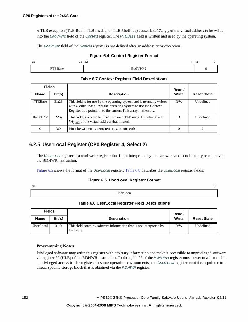
CP0 Registers of the 24K® Core
152 MIPS32® 24K® Processor Core Family Software User’s Manual, Revision 03.11
Copyright © 2004-2008 MIPS Technologies Inc. All rights reserved.
A TLB exception (TLB Refill, TLB Invalid, or TLB Modified) causes bits VA31:13 of the virtual address to be writteninto the BadVPN2 field of the Context register. The PTEBase field is written and used by the operating system.
The BadVPN2 field of the Context register is not defined after an address error exception.
Figure 6.4 Context Register Format
6.2.5 UserLocal Register (CP0 Register 4, Select 2)
The UserLocal register is a read-write register that is not interpreted by the hardware and conditionally readable viathe RDHWR instruction.
Figure 6.5 shows the format of the UserLocal register; Table 6.8 describes the UserLocal register fields.
Figure 6.5 UserLocal Register Format
Programming Notes
Privileged software may write this register with arbitrary information and make it accessible to unprivileged softwarevia register 29 (ULR) of the RDHWR instruction. To do so, bit 29 of the HWREna register must be set to a 1 to enableunprivileged access to the register. In some operating environments, the UserLocal register contains a pointer to athread-specific storage block that is obtained via the RDHWR register.
31 23 22 4 3 0
PTEBase BadVPN2 0
Table 6.7 Context Register Field Descriptions
Fields
DescriptionRead /Write Reset StateName Bit(s)
PTEBase 31:23 This field is for use by the operating system and is normally writtenwith a value that allows the operating system to use the ContextRegister as a pointer into the current PTE array in memory.
R/W Undefined
BadVPN2 22:4 This field is written by hardware on a TLB miss. It contains bitsVA31:13 of the virtual address that missed.
R Undefined
0 3:0 Must be written as zero; returns zero on reads. 0 0
31 0
UserLocal
Table 6.8 UserLocal Register Field Descriptions
Fields
DescriptionRead /Write Reset StateName Bit(s)
UserLocal 31:0 This field contains software information that is not interpreted byhardware.
R/W Undefined

6.2 CP0 Register Descriptions
MIPS32® 24K® Processor Core Family Software User’s Manual, Revision 03.11 153
Copyright © 2004-2008 MIPS Technologies Inc. All rights reserved.
6.2.6 PageMask Register (CP0 Register 5, Select 0)
The PageMask register is a read/write register used for reading from and writing to the TLB. It holds a comparisonmask that sets the variable page size for each TLB entry, as shown in Table 6.10.
This register is only valid with the TLB. It is reserved if the FM is implemented.
Figure 6.6 PageMask Register Format
Software may determine which page sizes are supported by writing all ones to the PageMask register, then readingthe value back. If a pair of bits reads back as ones, the processor implements that page size. The operation of the pro-cessor is UNDEFINED if software loads the Mask field with a value other than one of those listed in Table 6.10, evenif the hardware returns a different value on read. Hardware may depend on this requirement in implementing hard-ware structures.
31 29 28 13 12 0
0 Mask 0
Table 6.9 PageMask Register Field Descriptions
Fields
DescriptionRead /Write Reset StateName Bits
0 31:29,12:0
Ignored on write; returns zero on read. R 0
Mask 28:13 The Mask field is a bit mask in which a “1” bit indicates that the cor-responding bit of the virtual address should not participate in theTLB match.
R/W Undefined
Table 6.10 Values for the Mask Field of the PageMask Register
Page Size
Bit
28 27 26 25 24 23 22 21 20 19 18 17 16 15 14 13
4 KBytes 0 0 0 0 0 0 0 0 0 0 0 0 0 0 0 0
16 KBytes 0 0 0 0 0 0 0 0 0 0 0 0 0 0 1 1
64 KBytes 0 0 0 0 0 0 0 0 0 0 0 0 1 1 1 1
256 KBytes 0 0 0 0 0 0 0 0 0 0 1 1 1 1 1 1
1 MByte 0 0 0 0 0 0 0 0 1 1 1 1 1 1 1 1
4 MByte 0 0 0 0 0 0 1 1 1 1 1 1 1 1 1 1
16 MByte 0 0 0 0 1 1 1 1 1 1 1 1 1 1 1 1
64 MByte 0 0 1 1 1 1 1 1 1 1 1 1 1 1 1 1
256 MByte 1 1 1 1 1 1 1 1 1 1 1 1 1 1 1 1

CP0 Registers of the 24K® Core
154 MIPS32® 24K® Processor Core Family Software User’s Manual, Revision 03.11
Copyright © 2004-2008 MIPS Technologies Inc. All rights reserved.
6.2.7 Wired Register (CP0 Register 6, Select 0)
The Wired register is a read/write register that specifies the boundary between the wired and random entries in theTLB as shown in Figure 6.7. The width of the Wired field is calculated in the same manner as that described for theIndex register above. Wired entries are fixed, non-replaceable entries that are not overwritten by a TLBWR instruc-tion. Wired entries can be overwritten by a TLBWI instruction.
The Wired register is reset to zero by a Reset exception. Writing the Wired register causes the Random register toreset to its upper bound.
The operation of the processor is undefined if a value greater than or equal to the number of TLB entries is written tothe Wired register.
This register is only valid with a TLB. It is reserved when the FM is implemented.
Figure 6.7 Wired and Random Entries in the TLB
Figure 6.8 Wired Register Format
6.2.8 HWREna Register (CP0 Register 7, Select 0)
The HWREna register contains a bit mask that determines which hardware registers are accessible via the RDHWRinstruction when that instruction is executed in a mode in which coprocessor 0 is not enabled.
31 6 5 0
0 Wired
Table 6.11 Wired Register Field Descriptions
Fields
DescriptionRead /Write Reset StateName Bit(s)
0 31:6 Must be written as zero; returns zero on reads. 0 0
Wired 5:0 TLB wired boundary.For 16 and 32 entry TLBs, behavior is undefined if value is set to avalue larger than last TLB entry.
R/W 0
Ran
dom
Wire
d
Entry 0
Entry 10
Entry n-1
Wired Register 10

6.2 CP0 Register Descriptions
MIPS32® 24K® Processor Core Family Software User’s Manual, Revision 03.11 155
Copyright © 2004-2008 MIPS Technologies Inc. All rights reserved.
Figure 6.9 shows the format of the HWREna Register; Table 6.12 describes the HWREna register fields.
Figure 6.9 HWREna Register Format31 30 29 0
0 Mask
Table 6.12 HWREna Register Field Descriptions
Fields
DescriptionRead /Write Reset StateName Bits
0 31..30 Reserved 0 0
Mask 29..0 Each bit in this field enables access by the RDHWR instruction to aparticular hardware register (which may not be an actual register). Ifbit ‘n’ in this field is a 1, access is enabled to hardware register ‘n’.If bit ‘n’ of this field is a 0, access is disabled.Table 6.13 lists the RDHWR registers, and register number ‘n’ cor-responds to bit ‘n’ in this field.
R/W 0
Table 6.13 RDHWR Register Numbers
RegisterNumber Mnemonic Description
0 CPUNum This register provides read access to the coprocessor 0 EBaseCPUNum field.
1 SYNCI_Step Address step size to be used with the SYNCI instruction. See that instruction’sdescription for the use of this value. In the typical implementation, this value shouldbe zero if there are no caches in the system which must be synchronized (eitherbecause there are no caches, or because the instruction cache tracks writes to the datacache). In other cases, the return value should be the smallest line size of the cachesthat must be synchronized.For the 24K 24k, the SYNCI_Step value is 32 since the line size is 32 bytes.
2 CC High-resolution cycle counter. This register provides read access to the coprocessor 0Count Register.
3 CCRes Resolution of the CC register. This value denotes the number of cycles betweenupdate of the register. For example:
In the 24K 24k, the CCRes value is 2 to indicate that the CC register increments everysecond core cycle.
4-28These registers numbers are reserved for future architecture use. Access results in aReserved Instruction Exception.
CCRes Value Meaning
1 CC register increments every cycle
2 CC register increments every second cycle
3 CC register increments every third cycle
etc.

CP0 Registers of the 24K® Core
156 MIPS32® 24K® Processor Core Family Software User’s Manual, Revision 03.11
Copyright © 2004-2008 MIPS Technologies Inc. All rights reserved.
Using the HWREna register, privileged software may select which of the hardware registers are accessible via theRDHWR instruction. In doing so, a register may be virtualized at the cost of handling a Reserved Instruction Excep-tion, interpreting the instruction, and returning the virtualized value. For example, if it is not desirable to providedirect access to the Count register, access to that register may be individually disabled and the return value can be vir-tualized by the operating system.
Software may determine which registers are implemented by writing all ones to the HWREna register, then readingthe value back. If a bit reads back as a one, the processor implements that hardware register.
6.2.9 BadVAddr Register (CP0 Register 8, Select 0)
The BadVAddr register is a read-only register that captures the most recent virtual address that caused one of the fol-lowing exceptions:
• Address error (AdEL or AdES)
• TLB Refill
• TLB Invalid
• TLB Modified
The BadVAddr register does not capture address information for cache or bus errors, since they are not addressingerrors.
Figure 6.10 BadVAddr Register Format
29 ULR User Local Register. This register provides read access to the coprocessor 0UserLocal register. In some operating environments, the UserLocal register is apointer to a thread-specific storage block.
30-31These register numbers are reserved for future implementation-dependent use. Accessresults in a Reserved Instruction Exception.
31 0
BadVAddr
Table 6.14 BadVAddr Register Field Description
Fields
DescriptionRead /Write Reset StateName Bits
Bad-VAddr
31:0 Bad virtual address. R Undefined
Table 6.13 RDHWR Register Numbers
RegisterNumber Mnemonic Description

6.2 CP0 Register Descriptions
MIPS32® 24K® Processor Core Family Software User’s Manual, Revision 03.11 157
Copyright © 2004-2008 MIPS Technologies Inc. All rights reserved.
6.2.10 Count Register (CP0 Register 9, Select 0)
The Count register acts as a timer, incrementing at a constant rate, whether or not an instruction is executed, retired,or any forward progress is made through the pipeline. If enabled, the counter increments every other clock. Settingthe DC bit in the Cause register to 0 enables counting.
The Count register can be written for functional or diagnostic purposes, including at reset or to synchronize proces-sors.
By writing the CountDM bit in the Debug register, it is possible to control whether the Count register continues incre-menting while the processor is in debug mode.
Figure 6.11 Count Register Format
6.2.11 EntryHi Register (CP0 Register 10, Select 0)
The EntryHi register contains the virtual address match information used for TLB read, write, and access operations.
A TLB exception (TLB Refill, TLB Invalid, or TLB Modified) causes bits VA31..13 of the virtual address to be writteninto the VPN2 field of the EntryHi register. A TLBR instruction writes the EntryHi register with the correspondingfields from the selected TLB entry. The ASID field is written by software with the current address space identifiervalue and is used during the TLB comparison process to determine TLB match.
Because the ASID field is overwritten by a TLBR instruction, software must save and restore the value of ASIDaround use of the TLBR. This is especially important in TLB Invalid and TLB Modified exceptions, and in othermemory management software.
The VPN2 field of the EntryHi register is not defined after an address error exception and this field may be modifiedby hardware during the address error exception sequence. Software writes of the EntryHi register (via MTC0) do notcause the implicit write of address-related fields in the BadVAddr, Context registers.
This register is only valid with the TLB. It is reserved if the FM is implemented.
Figure 6.12 EntryHi Register Format
31 0
Count
Table 6.15 Count Register Field Description
Fields
DescriptionRead /Write Reset StateName Bits
Count 31:0 Interval counter. R/W Undefined
31 13 12 8 7 0
VPN2 0 ASID

CP0 Registers of the 24K® Core
158 MIPS32® 24K® Processor Core Family Software User’s Manual, Revision 03.11
Copyright © 2004-2008 MIPS Technologies Inc. All rights reserved.
6.2.12 Compare Register (CP0 Register 11, Select 0)
The Compare register acts in conjunction with the Count register to implement a timer and timer interrupt function.The timer interrupt is an output of the cores. The Compare register maintains a stable value and does not change on itsown.
When the value of the Count register equals the value of the Compare register, the SI_TimerInt pin is asserted. Thispin will remain asserted until the Compare register is written. The SI_TimerInt pin can be fed back into the core onone of the interrupt pins to generate an interrupt. Traditionally, this has been done by multiplexing it with hardwareinterrupt 5 to set interrupt bit IP(7) in the Cause register.
For diagnostic purposes, the Compare register is a read/write register. In normal use, however, the Compare registeris write-only. Writing a value to the Compare register, as a side effect, clears the timer interrupt.
Figure 6.13 Compare Register Format
6.2.13 Status Register (CP0 Register 12, Select 0)
The Status register is a read/write register that contains the operating mode, interrupt enabling, and the diagnosticstates of the processor. Fields of this register combine to create operating modes for the processor. Refer to Section4.2 “Modes of Operation” for a discussion of operating modes, and Section 5.3 “Interrupts” for a discussion of inter-rupt modes.
Interrupt Enable: Interrupts are enabled when all of the following conditions are true:
• IE = 1
Table 6.16 EntryHi Register Field Descriptions
Fields
DescriptionRead /Write Reset StateName Bits
VPN2 31..13 VA31..13 of the virtual address (virtual page number / 2). This field is
written by hardware on a TLB exception or on a TLB read, and iswritten by software before a TLB write.
R/W Undefined
0 12..8 Must be written as zero; returns zero on read. 0 0
ASID 7..0 Address space identifier. This field is written by hardware on a TLBread and by software to establish the current ASID value for TLBwrite and against which TLB references match each entry’s TLBASID field.
R/W Undefined
31 0
Compare
Table 6.17 Compare Register Field Description
Fields
DescriptionRead /Write Reset StateName Bit(s)
Compare 31:0 Interval count compare value. R/W Undefined

6.2 CP0 Register Descriptions
MIPS32® 24K® Processor Core Family Software User’s Manual, Revision 03.11 159
Copyright © 2004-2008 MIPS Technologies Inc. All rights reserved.
• EXL = 0
• ERL = 0
• DM = 0
If these conditions are met, then the settings of the IM and IE bits enable the interrupts.
6.2.13.1 Operating Modes
Debug Mode
The processor is operating in Debug Mode if the DM bit in the CP0 Debug register is a one. If the processor is runningin Debug Mode, it has full access to all resources that are available to Kernel Mode operation.
Kernel Mode
The processor is operating in Kernel Mode when the DM bit in the Debug register is a zero and any of the followingthree conditions is true:
• The KSU field in the CP0 Status register contains 2#00
• The EXL bit in the Status register is one
• The ERL bit in the Status register is one
The processor enters Kernel Mode at power-up, or as the result of an interrupt, exception, or error. The processorleaves Kernel Mode and enters User Mode or Supervisor Mode when all of the previous three conditions are false,usually as the result of an ERET instruction.
Supervisor Mode
The processor is operating in Supervisor Mode when all of the following conditions are true:
• The DM bit in the Debug register is a zero
• The KSU field in the Status register contains 2#01
• The EXL and ERL bits in the Status register are both zero
Supervisor mode is not supported with the Fixed Mapping MMU.
User Mode
The processor is operating in User Mode when all of the following conditions are true:
• The DM bit in the Debug register is a zero
• The KSU field in the Status register contains 2#10
• The EXL and ERL bits in the Status register are both zero

CP0 Registers of the 24K® Core
160 MIPS32® 24K® Processor Core Family Software User’s Manual, Revision 03.11
Copyright © 2004-2008 MIPS Technologies Inc. All rights reserved.
6.2.13.2 Coprocessor Accessibility
The Status register CU bits control coprocessor accessibility. If any coprocessor is unusable, then an instruction thataccesses it generates an exception.
Figure 6.14 Status Register Format31 28 27 26 25 24 23 22 21 20 19 18 17 16 15 10 9 8 7 6 5 4 3 2 1 0
CU3..CU0 RP FR RE MX R BEV TS SR NMI 0 CEE R IM7..IM2 IM1..IM0 R KSU ERL EXL IE
IPL
Table 6.18 Status Register Field Descriptions
Fields
DescriptionRead /Write Reset StateName Bits
CU3 31 Reserved. R 0
CU2 30 Controls access to Coprocessor 2
This bit can only be written when a coprocessor 2 unit is present.This bit cannot be written and will read as 0 if coprocessor 2 unit isnot presen.
R/W Undefined
CU1 29 Controls access to Coprocessor 1
This bit can only be written when the Floating Point Unit is present(24Kf core); in the 24Kc core, this bit cannot be written and willread as 0.
R/W Undefined
CU0 28 Controls access to coprocessor 0
Coprocessor 0 is always usable when the processor is running in ker-nel mode, independent of the state of the CU0 bit.
R/W Undefined
RP 27 Enables reduced power mode. The state of the RP bit is available onthe external 24k interface as the SI_RP signal.
R/W 0
Encoding Meaning
0 Access not allowed
1 Access allowed
Encoding Meaning
0 Access not allowed
1 Access allowed
Encoding Meaning
0 Access not allowed
1 Access allowed

6.2 CP0 Register Descriptions
MIPS32® 24K® Processor Core Family Software User’s Manual, Revision 03.11 161
Copyright © 2004-2008 MIPS Technologies Inc. All rights reserved.
FR 26 This bit is used to control the floating point register mode for 64-bitfloating point units:
This bit must be ignored on write and read as zero under the follow-ing conditions• No floating point unit is implemented• 64-bit floating point unit is not implemented
R/W 0
RE 25 Used to enable reverse-endian memory references while the proces-sor is running in user modeNot supported
R 0
MX 24 Enables access to DSP ASE resources. An attempt to execute anyDSP ASE instruction before this bit has been set to 1 will cause aDSP State Disabled exception.Since the DSP ASE is not present on the 24K core, this field isalways 0.
R 0
R 23 Reserved. This field is ignored on write and read as 0. R 0
BEV 22 Controls the location of exception vectors: R/W 1
TS 21 TLB shutdown. Indicates that a machine check exception was takendue to a TLBWI or TLBWR that would have created conflictingTLB entries. This bit is reserved if the TLB is not implemented.Software can only write a 0 to this bit to clear it and cannot force a0-1 transition.
R/W0 0
SR 20 Indicates that the entry through the reset exception vector was due toa Soft Reset. Soft Reset is not supported on this processor and thisbit is not writeable and will always read as 0
R 0
NMI 19 Indicates that the entry through the reset exception vector was due toan NMI:
Software can only write a 0 to this bit to clear it and cannot force a0-1 transition.
R/W0 1 for NMI; 0 oth-erwise
0 18 Must be written as zero; returns zero on read. 0 0
Table 6.18 Status Register Field Descriptions
Fields
DescriptionRead /Write Reset StateName Bits
Encoding Meaning
0 Floating point registers can contain any 32-bitdatatype. 64-bit datatypes are stored in even-oddpairs of registers
1 Floating point registers can contain any datatype
Encoding Meaning
0 Normal
1 Bootstrap
Encoding Meaning
0 Not NMI (Reset)
1 NMI

CP0 Registers of the 24K® Core
162 MIPS32® 24K® Processor Core Family Software User’s Manual, Revision 03.11
Copyright © 2004-2008 MIPS Technologies Inc. All rights reserved.
CEE 17 CorExtend Enable: This bit is sent to the CorExtend block to be usedto enable the CorExtend block. The usage of this signal by a CorEx-tend block is implementation dependent.This bit is reserved if CorExtend is not present.
R/W Undefined
R 16 Reserved. Ignored on write and read as zero. R 0
IM7..IM2 15..10 Interrupt Mask: Controls the enabling of each of the hardware inter-rupts. Refer to Section 5.3 “Interrupts” for a complete discussion ofenabled interrupts.An interrupt is taken if interrupts are enabled and the correspondingbits are set in both the Interrupt Mask field of the Status register andthe Interrupt Pending field of the Cause register and the IE bit is setin the Status register.
In implementations of Release 2 of the Architecture in which EICinterrupt mode is enabled (Config3VEIC = 1), these bits take on a
different meaning and are interpreted as the IPL field, describedbelow.
R/W Undefined
IPL 15..10 Interrupt Priority Level: In implementations of Release 2 of theArchitecture in which EIC interrupt mode is enabled (Config3VEIC= 1), this field is the encoded (0..63) value of the current IPL. Aninterrupt will be signaled only if the requested IPL is higher than thisvalue.If EIC interrupt mode is not enabled (Config3VEIC = 0), these bits
take on a different meaning and are interpreted as the IM7..IM2 bits,described above.
R/W Undefined
IM1..IM0 9..8 Interrupt Mask: Controls the enabling of each of the software inter-rupts. Refer to Section 5.3 “Interrupts” for a complete discussion ofenabled interrupts.
In implementations of Release 2 of the Architecture in which EICinterrupt mode is enabled (Config3VEIC = 1), these bits are writable,
but have no effect on the interrupt system.
R/W Undefined
R 7..5 Reserved. This field is ignored on write and read as 0. R 0
Table 6.18 Status Register Field Descriptions
Fields
DescriptionRead /Write Reset StateName Bits
Encoding Meaning
0 Interrupt request disabled
1 Interrupt request enabled
Encoding Meaning
0 Interrupt request disabled
1 Interrupt request enabled

6.2 CP0 Register Descriptions
MIPS32® 24K® Processor Core Family Software User’s Manual, Revision 03.11 163
Copyright © 2004-2008 MIPS Technologies Inc. All rights reserved.
KSU 4..3 This field denotes the base operating mode of the processor. SeeSection 4.2 “Modes of Operation” for a full discussion of operatingmodes. The encoding of this field is:
Note that the processor can also be in kernel mode if ERL or EXL isset, regardless of the state of the KSU field.
R/W Undefined
ERL 2 Error Level; Set by the processor when a Reset, Soft Reset, NMI orCache Error exception are taken.
When ERL is set:• The processor is running in kernel mode• Interrupts are disabled• The ERET instruction will use the return address held in
ErrorEPC instead of EPC
• The lower 229 bytes of kuseg are treated as an unmapped anduncached region. See Chapter 4, “Memory Management of the24K® Core” on page 87. This allows main memory to beaccessed in the presence of cache errors. The operation of the pro-cessor is UNDEFINED if the ERL bit is set while the processor isexecuting instructions from kuseg.
R/W 1
EXL 1 Exception Level; Set by the processor when any exception otherthan Reset, Soft Reset, or NMI exceptions is taken.
When EXL is set:• The processor is running in Kernel Mode• Interrupts are disabled.• TLB Refill exceptions use the general exception vector instead of
the TLB Refill vector.• EPC, CauseBD and SRSCtl (implementations of Release 2 of
the Architecture only) will not be updated if another exception istaken
R/W Undefined
Table 6.18 Status Register Field Descriptions
Fields
DescriptionRead /Write Reset StateName Bits
Encoding Meaning
00 Base mode is Kernel Mode
01 Base mode is Supervisor Mode
10 Base mode is User Mode
11 Reserved
Encoding Meaning
0 Normal level
1 Error level
Encoding Meaning
0 Normal level
1 Exception level

CP0 Registers of the 24K® Core
164 MIPS32® 24K® Processor Core Family Software User’s Manual, Revision 03.11
Copyright © 2004-2008 MIPS Technologies Inc. All rights reserved.
6.2.14 IntCtl Register (CP0 Register 12, Select 1)
The IntCtl register controls the expanded interrupt capability added in Release 2 of the Architecture, including vec-tored interrupts and support for an external interrupt controller. This register does not exist in implementations ofRelease 1 of the Architecture.
Figure 6.15 IntCtl Register Format
IE 0 Interrupt Enable: Acts as the master enable for software and hard-ware interrupts:
In Release 2 of the Architecture, this bit may be modified separatelyvia the DI and EI instructions.
R/W Undefined
31 29 28 26 25 10 9 5 4 0
IPTI IPPCI 0 VS 0
Table 6.19 IntCtl Register Field Descriptions
Fields
DescriptionRead /Write Reset StateName Bits
IPTI 31:29 For Interrupt Compatibility and Vectored Interrupt modes, this fieldspecifies the IP number to which the Timer Interrupt request ismerged, and allows software to determine whether to considerCauseTI for a potential interrupt.
The value of this bit is set by the static input, SI_IPTI[2:0]. Thisallows external logic to communicate the specific SI_Int hardwareinterrupt pin to which the SI_TimerInt signal is attached.The value of this field is not meaningful if External Interrupt Con-troller Mode is enabled. The external interrupt controller is expectedto provide this information for that interrupt mode.
R Externally Set
Table 6.18 Status Register Field Descriptions
Fields
DescriptionRead /Write Reset StateName Bits
Encoding Meaning
0 Interrupts are disabled
1 Interrupts are enabled
Encoding IP bit Hardware Interrupt Source
2 2 HW0
3 3 HW1
4 4 HW2
5 5 HW3
6 6 HW4
7 7 HW5

6.2 CP0 Register Descriptions
MIPS32® 24K® Processor Core Family Software User’s Manual, Revision 03.11 165
Copyright © 2004-2008 MIPS Technologies Inc. All rights reserved.
6.2.15 SRSCtl Register (CP0 Register 12, Select 2)
The SRSCtl register controls the operation of GPR shadow sets in the processor.
Figure 6.16 SRSCtl Register Format
IPPCI 28:26 For Interrupt Compatibility and Vectored Interrupt modes, this fieldspecifies the IP number to which the Performance Counter Interruptrequest is merged, and allows software to determine whether to con-sider CausePCI for a potential interrupt.
The value of this bit is set by the static input, SI_IPPCI[2:0]. Thisallows external logic to communicate the specific SI_Int hardwareinterrupt pin to which the SI_PCInt signal is attached.The value of this field is not meaningful if External Interrupt Con-troller Mode is enabled. The external interrupt controller is expectedto provide this information for that interrupt mode.
R Externally Set
VS 9:5 Vector Spacing. If vectored interrupts are implemented (as denotedby Config3VInt or Config3VEIC), this field specifies the spacing
between vectored interrupts.
All other values are reserved. The operation of the processor isUNDEFINED if a reserved value is written to this field.
R/W 0
0 25:10, 4:0 Must be written as zero; returns zero on read. 0 0
31 30 29 26 25 22 21 18 17 16 15 12 11 10 9 6 5 4 3 0
0 HSS 0 EICSS 0 ESS 0 PSS 0 CSS
Table 6.19 IntCtl Register Field Descriptions (Continued)
Fields
DescriptionRead /Write Reset StateName Bits
Encoding IP bit Hardware Interrupt Source
2 2 HW0
3 3 HW1
4 4 HW2
5 5 HW3
6 6 HW4
7 7 HW5
EncodingSpacing Between
Vectors (hex)Spacing BetweenVectors (decimal)
16#00 16#000 0
16#01 16#020 32
16#02 16#040 64
16#04 16#080 128
16#08 16#100 256
16#10 16#200 512

CP0 Registers of the 24K® Core
166 MIPS32® 24K® Processor Core Family Software User’s Manual, Revision 03.11
Copyright © 2004-2008 MIPS Technologies Inc. All rights reserved.
Table 6.20 SRSCtl Register Field Descriptions
Fields
DescriptionRead /Write Reset StateName Bits
HSS 29:26 Highest Shadow Set. This field contains the highest shadow setnumber that is implemented by this processor. A value of zero in thisfield indicates that only the normal GPRs are implemented.Possible values of this field for the 24K processor are:
The value in this field also represents the highest value that can bewritten to the ESS, EICSS, PSS, and CSS fields of this register, orto any of the fields of the SRSMap register. The operation of theprocessor is UNDEFINED if a value larger than the one in this fieldis written to any of these other fields.
R Preset
EICSS 21:18 EIC interrupt mode shadow set. If Config3VEIC is 1 (EIC interrupt
mode is enabled), this field is loaded from the external interrupt con-troller for each interrupt request and is used in place of the SRSMapregister to select the current shadow set for the interrupt.See Section 5.3.1.3 “External Interrupt Controller Mode” for a dis-cussion of EIC interrupt mode. If Config3VEIC is 0, this field returns
zero on read.
R Undefined
ESS 15:12 Exception Shadow Set. This field specifies the shadow set to use onentry to Kernel Mode caused by any exception other than a vectoredinterrupt.The operation of the processor is UNDEFINED if software writes avalue into this field that is greater than the value in the HSS field.
R/W 0
PSS 9:6 Previous Shadow Set. If GPR shadow registers are implemented,and with the exclusions noted in the next paragraph, this field is cop-ied from the CSS field when an exception or interrupt occurs. AnERET instruction copies this value back into the CSS field ifStatusBEV = 0.
This field is not updated on any exception which sets StatusERL to 1
(i.e., Reset, Soft Reset, NMI, cache error), an entry into EJTAGDebug mode, or any exception or interrupt that occurs withStatusEXL = 1, or StatusBEV = 1. This field is not updated on an
exception that occurs while StatusERL = 1.
The operation of the processor is UNDEFINED if software writes avalue into this field that is greater than the value in the HSS field.
R/W 0
Encoding Meaning
0 One shadow set (normal GPR set) is present.
1 Two shadow sets are present.
3 Four shadow sets are present.
2, 3-15 Reserved

6.2 CP0 Register Descriptions
MIPS32® 24K® Processor Core Family Software User’s Manual, Revision 03.11 167
Copyright © 2004-2008 MIPS Technologies Inc. All rights reserved.
6.2.16 SRSMap Register (CP0 Register 12, Select 3)
The SRSMap register contains 8 4-bit fields that provide the mapping from an vector number to the shadow set num-ber to use when servicing such an interrupt. The values from this register are not used for a non-interrupt exception,or a non-vectored interrupt (CauseIV = 0 or IntCtlVS = 0). In such cases, the shadow set number comes fromSRSCtlESS.
If SRSCtlHSS is zero, the results of a software read or write of this register are UNPREDICTABLE.
The operation of the processor is UNDEFINED if a value is written to any field in this register that is greater than thevalue of SRSCtlHSS.
CSS 3:0 Current Shadow Set. If GPR shadow registers are implemented, thisfield is the number of the current GPR set. With the exclusions notedin the next paragraph, this field is updated with a new value on anyinterrupt or exception, and restored from the PSS field on an ERET.Table 6.21 describes the various sources from which the CSS field isupdated on an exception or interrupt.This field is not updated on any exception which sets StatusERL to1 (i.e., Reset, Soft Reset, NMI, cache error), an entry into EJTAGDebug mode, or any exception or interrupt that occurs withStatusEXL = 1, or StatusBEV = 1. Neither is it updated on an ERET
with StatusERL = 1 or StatusBEV = 1. This field is not updated on
an exception that occurs while StatusERL = 1.
The value of CSS can be changed directly by software only by writ-ing the PSS field and executing an ERET instruction.
R 0
0 31:30,25:22,17:16,
11:10, 5:4
Must be written as zeros; returns zero on read. 0 0
Table 6.21 Sources for new SRSCtlCSS on an Exception or Interrupt
Exception Type Condition SRSCtlCSS Source Comment
Exception All SRSCtlESS
Non-Vectored Interrupt CauseIV = 0 SRSCtlESS Treat as exception
Vectored Interrupt CauseIV = 1 and
Config3VEIC = 0 and
Config3VInt = 1
SRSMapVECTNUM Source is internal map regis-ter.(for VECTNUM see Table 5.4)
Vectored EIC Interrupt CauseIV = 1 and
Config3VEIC = 1
SRSCtlEICSS Source is external interruptcontroller.
Table 6.20 SRSCtl Register Field Descriptions (Continued)
Fields
DescriptionRead /Write Reset StateName Bits

CP0 Registers of the 24K® Core
168 MIPS32® 24K® Processor Core Family Software User’s Manual, Revision 03.11
Copyright © 2004-2008 MIPS Technologies Inc. All rights reserved.
The SRSMap register contains the shadow register set numbers for vector numbers 7..0. The same shadow set num-ber can be established for multiple interrupt vectors, creating a many-to-one mapping from a vector to a singleshadow register set number.
Figure 6.17 SRSMap Register Format
6.2.17 Cause Register (CP0 Register 13, Select 0)
The Cause register primarily describes the cause of the most recent exception. In addition, fields also control soft-ware interrupt requests and the vector through which interrupts are dispatched. With the exception of the IP1..0, DC,IV, and WP fields, all fields in the Cause register are read-only. Release 2 of the Architecture added optional supportfor an External Interrupt Controller (EIC) interrupt mode, in which IP7..2 are interpreted as the Requested InterruptPriority Level (RIPL).
Figure 6.18 Cause Register Format
31 28 27 24 23 20 19 16 15 12 11 8 7 4 3 0
SSV7 SSV6 SSV5 SSV4 SSV3 SSV2 SSV1 SSV0
Table 6.22 SRSMap Register Field Descriptions
Fields
DescriptionRead /Write Reset StateName Bits
SSV7 31..28 Shadow register set number for Vector Number 7 R/W 0
SSV6 27..24 Shadow register set number for Vector Number 6 R/W 0
SSV5 23..20 Shadow register set number for Vector Number 5 R/W 0
SSV4 19..16 Shadow register set number for Vector Number 4 R/W 0
SSV3 15..12 Shadow register set number for Vector Number 3 R/W 0
SSV2 11..8 Shadow register set number for Vector Number 2 R/W 0
SSV1 7..4 Shadow register set number for Vector Number 1 R/W 0
SSV0 3..0 Shadow register set number for Vector Number 0 R/W 0
31 30 29 28 27 26 25 24 23 22 21 16 15 10 9 8 7 6 2 1 0
BD TI CE DC PCI 0 IV WP 0 IP7..IP2 IP1..IP0 0 Exc Code 0
RIPL

6.2 CP0 Register Descriptions
MIPS32® 24K® Processor Core Family Software User’s Manual, Revision 03.11 169
Copyright © 2004-2008 MIPS Technologies Inc. All rights reserved.
Table 6.23 Cause Register Field Descriptions
Fields
DescriptionRead /Write Reset StateName Bits
BD 31 Indicates whether the last exception taken occurred in a branch delayslot:
The processor updates BD only if StatusEXL was zero when the
exception occurred.
R Undefined
TI 30 Timer Interrupt. This bit denotes whether a timer interrupt is pend-ing (analogous to the IP bits for other interrupt types):
The state of the TI bit is available on the external core interface asthe SI_TimerInt signal.
R Undefined
CE 29:28 Coprocessor unit number referenced when a Coprocessor Unusableexception is taken. This field is loaded by hardware on every excep-tion, but is UNPREDICTABLE for all exceptions except forCoprocessor Unusable.
R Undefined
DC 27 Disable Count register. In some power-sensitive applications, theCount register is not used and is the source of meaningful powerdissipation. This bit allows the Count register to be stopped in suchsituations.
R/W 0
PCI 26 Performance Counter Interrupt: This bit denotes whether a perfor-mance counter interrupt is pending (analogous to the IP bits forother interrupt types):
The state of the PCI bit is available on the external core interface asthe SI_PCInt signal.
R Undefined
IV 23 Indicates whether an interrupt exception uses the general exceptionvector or a special interrupt vector:
If the CauseIV is 1 and StatusBEV is 0, the special interrupt vector
represents the base of the vectored interrupt table.
R/W Undefined
Encoding Meaning
0 Not in delay slot
1 In delay slot
Encoding Meaning
0 No timer interrupt is pending
1 Timer interrupt is pending
Encoding Meaning
0 Enable counting of Count register
1 Disable counting of Count register
Encoding Meaning
0 No performance counter interrupt is pending
1 Performance counter interrupt is pending
Encoding Meaning
0 Use the general exception vector (16#180)
1 Use the special interrupt vector (16#200)

CP0 Registers of the 24K® Core
170 MIPS32® 24K® Processor Core Family Software User’s Manual, Revision 03.11
Copyright © 2004-2008 MIPS Technologies Inc. All rights reserved.
WP 22 Indicates that a watch exception was deferred because StatusEXL or
StatusERL were a one at the time the watch exception was detected.
This bit both indicates that the watch exception was deferred, andcauses the exception to be initiated once StatusEXL and StatusERLare both zero. As such, software must clear this bit as part of thewatch exception handler to prevent a watch exception loop.Software should not write a 1 to this bit when its value is a 0, therebycausing a 0-to-1 transition. If such a transition is caused by software,it is UNPREDICTABLE whether hardware ignores the write,accepts the write with no side effects, or accepts the write and ini-tiates a watch exception once StatusEXL and StatusERL are both
zero.
R/W Undefined
IP7..IP2 15:10 Indicates an interrupt is pending:
If EIC interrupt mode is not enabled (Config3VEIC = 0), timer inter-
rupts are combined in a system-dependent way with any hardwareinterrupt. If EIC interrupt mode is enabled (Config3VEIC = 1), these
bits take on a different meaning and are interpreted as the RIPLfield, described below.See Section 5.3 “Interrupts” for a general description of interruptprocessing.
R Undefined
RIPL 15:10 Requested Interrupt Priority Level: If EIC interrupt mode is enabled(Config3VEIC = 1), this field is the encoded (0..63) value of the
requested interrupt. A value of zero indicates that no interrupt isrequested.If EIC interrupt mode is not enabled (Config3VEIC = 0), these bits
take on a different meaning and are interpreted as the IP7..IP2 bits,described above.
R Undefined
IP1..IP0 9:8 Controls the request for software interrupts:
These bits are exported to an external interrupt controller for prioriti-zation in EIC interrupt mode with other interrupt sources. The stateof these bits is available on the external core interface as theSI_SWInt[1:0] bus.
R/W Undefined
ExcCode 6:2 Exception code - see Table 6.24 R Undefined
Table 6.23 Cause Register Field Descriptions (Continued)
Fields
DescriptionRead /Write Reset StateName Bits
Bit Name Meaning
15 IP7 Hardware interrupt 5
14 IP6 Hardware interrupt 4
13 IP5 Hardware interrupt 3
12 IP4 Hardware interrupt 2
11 IP3 Hardware interrupt 1
10 IP2 Hardware interrupt 0
Bit Name Meaning
9 IP1 Request software interrupt 1
8 IP0 Request software interrupt 0

6.2 CP0 Register Descriptions
MIPS32® 24K® Processor Core Family Software User’s Manual, Revision 03.11 171
Copyright © 2004-2008 MIPS Technologies Inc. All rights reserved.
0 25:24,21:16, 7,
1:0
Must be written as zero; returns zero on read. 0 0
Table 6.24 Cause Register ExcCode Field
Exception Code Value
Mnemonic DescriptionDecimal Hexadecimal
0 16#00 Int Interrupt
1 16#01 Mod TLB modification exception
2 16#02 TLBL TLB exception (load or instruction fetch)
3 16#03 TLBS TLB exception (store)
4 16#04 AdEL Address error exception (load or instruction fetch)
5 16#05 AdES Address error exception (store)
6 16#06 IBE Bus error exception (instruction fetch)
7 16#07 DBE Bus error exception (data reference: load or store)
8 16#08 Sys Syscall exception
9 16#09 Bp Breakpoint exception. If an SDBBP instruction is executed while the pro-cessor is running in EJTAG Debug Mode, this value is written to theDebugDExcCode field to denote an SDBBP in Debug Mode.
10 16#0a RI Reserved instruction exception
11 16#0b CpU Coprocessor Unusable exception
12 16#0c Ov Arithmetic Overflow exception
13 16#0d Tr Trap exception
14 16#0e - Reserved
15 16#0f FPE Floating point exception
16 16#10 IS1 Coprocessor 2 implementation specific exception
17 16#11 CEU CorExtend Unusable
18 16#12 C2E Precise Coprocessor 2 exception
19-22 16#13-16#16 - Reserved
23 16#17 WATCH Reference to WatchHi/WatchLo address
24 16#18 MCheck Machine checkcore
25-29 16#19-16#1d - Reserved
30 16#1e CacheErr Cache error. In normal mode, a cache error exception has a dedicatedvector and the Cause register is not updated. If a cache error occurs whilein Debug Mode, this code is written to the DebugDExcCode field to indi-
cate that re-entry to Debug Mode was caused by a cache error.
Table 6.23 Cause Register Field Descriptions (Continued)
Fields
DescriptionRead /Write Reset StateName Bits

CP0 Registers of the 24K® Core
172 MIPS32® 24K® Processor Core Family Software User’s Manual, Revision 03.11
Copyright © 2004-2008 MIPS Technologies Inc. All rights reserved.
6.2.18 Exception Program Counter (CP0 Register 14, Select 0)
The Exception Program Counter (EPC) is a read/write register that contains the address at which processing resumesafter an exception has been serviced. All bits of the EPC register are significant and must be writable.
For synchronous (precise) exceptions, the EPC contains one of the following:
• The virtual address of the instruction that was the direct cause of the exception
• The virtual address of the immediately preceding branch or jump instruction, when the exception causinginstruction is in a branch delay slot and the Branch Delay bit in the Cause register is set.
On new exceptions, the processor does not write to the EPC register when the EXL bit in the Status register is set,however, the register can still be written via the MTC0 instruction.
In processors that implement the MIPS16 ASE, a read of the EPC register (via MFC0) returns the following value inthe destination GPR:
GPR[rt] ← ExceptionPC31..1 || ISAMode0
That is, the upper 31 bits of the exception PC are combined with the lower bit of the ISAMode field of DEPC7 andwritten to the GPR.
Similarly, a write to the EPC register (via MTC0) takes the value from the GPR and distributes that value to theexception PC and the ISAMode field, as follows
ExceptionPC ← GPR[rt]31..1 || 0ISAMode ← 2#0 || GPR[rt]0
That is, the upper 31 bits of the GPR are written to the upper 31 bits of the exception PC, and the lower bit of theexception PC is cleared. The upper bit of the ISAMode field is cleared and the lower bit is loaded from the lower bit ofthe GPR.
Figure 6.19 EPC Register Format
31 16#1f - Reserved
31 0
EPC
Table 6.25 EPC Register Field Description
Fields
DescriptionRead /Write Reset StateName Bit(s)
EPC 31:0 Exception Program Counter. R/W Undefined
Table 6.24 Cause Register ExcCode Field (Continued)
Exception Code Value
Mnemonic DescriptionDecimal Hexadecimal

6.2 CP0 Register Descriptions
MIPS32® 24K® Processor Core Family Software User’s Manual, Revision 03.11 173
Copyright © 2004-2008 MIPS Technologies Inc. All rights reserved.
6.2.19 Processor Identification (CP0 Register 15, Select 0)
The Processor Identification (PRId) register is a 32 bit read-only register that contains information identifying themanufacturer, manufacturer options, processor identification, and revision level of the processor.
Figure 6.20 PRId Register Format
6.2.20 EBase Register (CP0 Register 15, Select 1)
The EBase register is a read/write register containing the base address of the exception vectors used when StatusBEVequals 0, and a read-only CPU number value that may be used by software to distinguish different processors in amulti-processor system.
The EBase register provides the ability for software to identify the specific processor within a multi-processor sys-tem, and allows the exception vectors for each processor to be different, especially in systems composed of heteroge-neous processors. Bits 31:12 of the EBase register are concatenated with zeros to form the base of the exceptionvectors when StatusBEV is 0. The exception vector base address comes from the fixed defaults (see Section5.5 “Exception Vector Locations”) when StatusBEV is 1, or for any EJTAG Debug exception. The reset state of bits
31 24 23 16 15 8 7 0
CompanyOption Company ID Processor ID Revision
Table 6.26 PRId Register Field Descriptions
Fields
DescriptionRead /Write Reset StateName Bit(s)
CompanyOption
31:24 Implementation specific values R Preset
CompanyID
23:16 Identifies the company that designed or manufactured the processor.In the 24K this field contains a value of 1 to indicate MIPS Technol-ogies, Inc.
R 1
ProcessorID
15:8 Identifies the type of processor. This field allows software to distin-guish between the various types of MIPS Technologies processors.
R 0x93
Revision 7:0 Specifies the revision number of the processor. This field allowssoftware to distinguish between one revision and another of thesame processor type.This field is broken up into the following three subfields:
R Preset
Bit(s) Name Meaning
7:5 MajorRevision
This number is increased on major revisionsof the processor 24k
4:2 MinorRevision
This number is increased on each incremen-tal revision of the processor and reset oneach new major revision
1:0 PatchLevel
If a patch is made to modify an older revi-sion of the processor, this field will beincremented

CP0 Registers of the 24K® Core
174 MIPS32® 24K® Processor Core Family Software User’s Manual, Revision 03.11
Copyright © 2004-2008 MIPS Technologies Inc. All rights reserved.
31:12 of the EBase register initialize the exception base register to 16#8000.0000, providing backward compati-bility with Release 1 implementations.
Bits 31:30 of the EBase Register are fixed with the value 2#10 to force the exception base address to be in the kseg0or kseg1 unmapped virtual address segments. Bit 29 of exception base address will be forced to 1 on Cache Errorexceptions so the exception handler will be executed from the uncached kseg1 segment.
If the value of the exception base register is to be changed, this must be done with StatusBEV equal 1. The operationof the processor is UNDEFINED if the Exception Base field is written with a different value when StatusBEV is 0.
Combining bits 31:12 with the Exception Base field allows the base address of the exception vectors to be placed atany 4KBbyte page boundary.
Figure 6.21 EBase Register Format
6.2.21 Config Register (CP0 Register 16, Select 0)
The Config register specifies various configuration and capabilities information. Most of the fields in the Config reg-ister are initialized by hardware during the Reset exception process, or are constant. The K0, KU, and K23 fields mustbe initialized by software in the Reset exception handler, if the reset value is not desired.
Figure 6.22 Config Register Format — Select 0
31 30 29 12 11 10 9 0
1 0 Exception Base 0 CPUNum
Table 6.27 EBase Register Field Descriptions
Fields
DescriptionRead /Write Reset StateName Bits
1 31 This bit is ignored on write and returns one on read. R 1
ExceptionBase
29:12 In conjunction with bits 31..30, this field specifies the base addressof the exception vectors when StatusBEV is zero.
R/W 0
CPUNum 9:0 This field contains an identifier that will be unique among the CPUsin a multi-processor system. This can be used by software to distin-guish where it is running. The value in this field is set by theSI_CPUNum[9:0] static input pins to the core. .
R Externally Set
0 30, 11:10 Must be written as zero; returns zero on read. 0 0
31 30 28 27 25 24 23 22 21 20 19 18 17 16 15 14 13 12 10 9 7 6 3 2 0
M K23 KU ISP DSP UDI SB 0 MM 0 BM BE AT AR MT 0 K0
Table 6.28 Config Register Field Descriptions
Fields
DescriptionRead /Write Reset StateName Bit(s)
M 31 This bit is hardwired to ‘1’ to indicate the presence of the Config1register.
R 1

6.2 CP0 Register Descriptions
MIPS32® 24K® Processor Core Family Software User’s Manual, Revision 03.11 175
Copyright © 2004-2008 MIPS Technologies Inc. All rights reserved.
K23 30:28 This field controls the cacheability of the kseg2 and kseg3 addresssegments in FM implementations.Refer to Table 6.29 for the field encoding.
FM: R/WTLB: R
FM: 010TLB: 000
KU 27:25 This field controls the cacheability of the kuseg and useg addresssegments in FM implementations.Refer to Table 6.29 for the field encoding.
FM: R/WTLB: R
FM: 010TLB: 000
ISP 24 I-side ScratchPad RAM present R Preset
DSP 23 D-side ScratchPad RAM present R Preset
UDI 22 This bit indicates that CorExtend User Defined Instructions havebeen implemented.
R Preset
SB 21 Indicates whether SimpleBE bus mode is enabled. Set viaSI_SimpleBE input pin.
R Externally Set
MM 18 This bit indicates whether write-through merging is enabled in the32-byte collapsing write buffer.
R/W 1
BM 16 Burst order. Set via SI_SBlock input pin. R Externally Set
BE 15 Indicates the endian mode in which the processor is running. Set viaSI_Endian input pin.
R Externally Set
AT 14:13 Architecture type implemented by the processor. This field is always00 to indicate the MIPS32 architecture.
R 00
Table 6.28 Config Register Field Descriptions (Continued)
Fields
DescriptionRead /Write Reset StateName Bit(s)
Encoding Description
0 No User Defined Instructions are implemented
1 User Defined Instructions are implemented
Encoding Description
0 No reserved byte enables on OCP interface
1 Only simple byte enables allowed on OCP interface
Encoding Description
0 No Merging
1 Merging allowed
Encoding Description
0 Sequential
1 SubBlock
Encoding Description
0 Little endian
1 Big endian

CP0 Registers of the 24K® Core
176 MIPS32® 24K® Processor Core Family Software User’s Manual, Revision 03.11
Copyright © 2004-2008 MIPS Technologies Inc. All rights reserved.
6.2.22 Config1 Register (CP0 Register 16, Select 1)
The Config1 register is an adjunct to the Config register and encodes additional information about capabilities presenton the core. All fields in the Config1 register are read-only.
The instruction and data cache configuration parameters include encodings for the number of sets per way, the linesize, and the associativity. The total cache size for a cache is therefore:
Associativity * Line Size * Sets Per Way
AR 12:10 Architecture revision level. This field is always 001 to indicateMIPS32 Release 2.
R 001
MT 9:7 MMU Type: R Preset
K0 2:0 Kseg0 coherency algorithm. Refer to Table 6.29 for the field encod-ing.
R/W 010
0 20:19, 17,6:3
Must be written as zeros; returns zeros on reads. 0 0
Table 6.29 Cache Coherency Attributes
K0(2:0) Value Cache Coherency Attribute
0 Cacheable, noncoherent, write-through, no write allocate
1 Reserved
2 Uncached
3 Cacheable, noncoherent, write-back, write allocate
4,5,6 Reserved
7 Uncached Accelerated
Table 6.28 Config Register Field Descriptions (Continued)
Fields
DescriptionRead /Write Reset StateName Bit(s)
Encoding Description
0 Release 1
1 Release 2
2:7 Reserved
Encoding Description
1 Standard TLB
3 Fixed Mapping
0, 2, 4:7 Reserved

6.2 CP0 Register Descriptions
MIPS32® 24K® Processor Core Family Software User’s Manual, Revision 03.11 177
Copyright © 2004-2008 MIPS Technologies Inc. All rights reserved.
If the line size is zero, no cache is implemented.
Figure 6.23 Config1 Register Format31 30 25 24 22 21 19 18 16 15 13 12 10 9 7 6 5 4 3 2 1 0
M MMU Size IS IL IA DS DL DA C2 MD PC WR CA EP FP
Table 6.30 Config1 Register Field Descriptions
Fields
DescriptionRead /Write Reset StateName Bit(s)
M 31 This bit is hardwired to ‘1’ to indicate the presence of the Config2register.
R 1
MMUSize
30:25 This field contains the number of entries in the TLB minus one. Thefield is read as 0 decimal if the TLB is not implemented
R Preset
IS 24:22 This field contains the number of instruction cache sets per way. Thecorresponding total instruction cache size is shown in parentheses
R Preset
IL 21:19 This field contains the instruction cache line size The cache line sizeis fixed at 32 bytes when the I-Cache is present. A value of 0 indi-cates no ICache.
R Preset
IA 18:16 This field contains the level of instruction cache associativity Thisfield is fixed at 4-way set associative
R 0x3
DS 15:13 This field contains the number of data cache sets per way. The corre-sponding total data cache size is shown in parentheses
R Preset
Encoding Description
0x0 64 (8KB )
0x1 128 (16KB)
0x2 256 (32KB)
0x3 512 (64KB)
0x4:0x7 Reserved
Encoding Description
0x0 No ICache present
0x1:0x3 Reserved
0x4 32 bytes
0x5:0x7 Reserved
Encoding Description
0x0:0x2 Reserved
0x3 4-way
0x4:0x7 Reserved
Encoding Description
0x0 64 (8KB )
0x1 128 (16KB)
0x2 256 (32KB)
0x3 512 (64KB)
0x4:0x7 Reserved

CP0 Registers of the 24K® Core
178 MIPS32® 24K® Processor Core Family Software User’s Manual, Revision 03.11
Copyright © 2004-2008 MIPS Technologies Inc. All rights reserved.
6.2.23 Config2 Register (CP0 Register 16, Select 2)
The Config2 register is an adjunct to the Config register and is reserved to encode additional capabilities information.Config2 is allocated for showing the configuration of level 2/3 caches. L2 values reflect the configuration information
DL 12:10 This field contains the data cache line size. The cache line size isfixed at 32 bytes when a D-cache is present. This field reads 0 whena D-cache is not present.
R Preset
DA 9:7 This field contains the type of set associativity for the data cacheThe associativity is fixed at 4-way.
R 0x3
C2 6 Coprocessor 2 present. R Preset
MD 5 MDMX implemented. R 0
PC 4 Performance Counter registers implemented. R 1
WR 3 Watch registers implemented. R 1
CA 2 Code compression (MIPS16) implemented. R 1
EP 1 EJTAG present: This bit is always set to indicate that the core imple-ments EJTAG.
R 1
FP 0 FPU implemented. R Preset
Table 6.30 Config1 Register Field Descriptions (Continued)
Fields
DescriptionRead /Write Reset StateName Bit(s)
Encoding Description
0x0 No DCache present
0x1:0x3 Reserved
0x4 32 bytes
0x5:0x7 Reserved
Encoding Description
0x0:0x2 Reserved
0x3 4-way
0x4:0x7 Reserved
Encoding Description
0 Coprocessor2 not present
1 Coprocessor2 present
Encoding Description
0 No Watch registers are present
1 One or more Watch registers are present
Encoding Description
0 No MIPS16 present
1 MIPS16 is implemented

6.2 CP0 Register Descriptions
MIPS32® 24K® Processor Core Family Software User’s Manual, Revision 03.11 179
Copyright © 2004-2008 MIPS Technologies Inc. All rights reserved.
input from the L2 module. L3 fields are reset to 0 because L3 caches are not supported by the 24K core. All fields inthe Config2 register are read-only.
Figure 6.24 Config2 Register Format31 30 28 27 24 23 20 19 16 15 13 12 11 8 7 4 3 0
M TU TS TL TA SU L2B SS SL SA
Table 6.31 Config2 Register Field Descriptions
Fields
DescriptionRead /Write Reset StateName Bit(s)
M 31 This bit is hardwired to ‘1’ to indicate the presence of the Config3register.
R 1
TU 30:28 Implementation specific tertiary cache control. Tertiary cache notsupported
R 0
TS 27:24 Tertiary cache sets per way. Tertiary cache not supported R 0
TL 23:20 Tertiary cache line size. Tertiary cache not supported R 0
TA 19:16 Tertiary cache associativity. Tertiary cache not supported R 0
SU 15:13 Reserved R 0
L2B 12 L2 Bypass/L2_Bypassed. In systems which include an L2 cache,writing a 1 to this bit, will set the L2_Bypass output from the core.Setting the L2_Bypass output, directs the L2 cache to go intobypass mode. L2 responds by asserting its L2_Bypassed outputpin. The value of L2_Bypassed is returned when L2B is read.Since this involves a communication between CPU and L2, readingthis bit will reflect the new value with some implementation- andclock ratio- dependent delay.
R/W 0
SS 11:8 Secondary cache sets per way R Preset
Encoding Description
0 64
1 128
2 256
3 512
4 1024
5 2048
6 4096
7 8192
8-15 Reserved
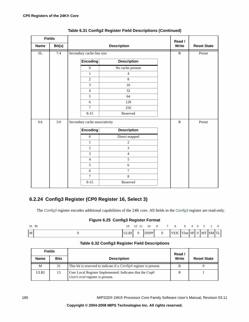
CP0 Registers of the 24K® Core
180 MIPS32® 24K® Processor Core Family Software User’s Manual, Revision 03.11
Copyright © 2004-2008 MIPS Technologies Inc. All rights reserved.
6.2.24 Config3 Register (CP0 Register 16, Select 3)
The Config3 register encodes additional capabilities of the 24K core. All fields in the Config3 register are read-only.
Figure 6.25 Config3 Register Format
SL 7:4 Secondary cache line size R Preset
SA 3:0 Secondary cache associativity R Preset
31 30 13 12 11 10 9 7 6 5 4 3 2 1 0
M 0 ULRI 0 DSPP 0 VEIC VInt SP 0 MT SM TL
Table 6.32 Config3 Register Field Descriptions
Fields
DescriptionRead /Write Reset StateName Bits
M 31 This bit is reserved to indicate if a Config4 register is present. R 0
ULRI 13 User Local Register Implemented: Indicates that the Cop0UserLocal register is present.
R 1
Table 6.31 Config2 Register Field Descriptions (Continued)
Fields
DescriptionRead /Write Reset StateName Bit(s)
Encoding Description
0 No cache present
1 4
2 8
3 16
4 32
5 64
6 128
7 256
8-15 Reserved
Encoding Description
0 Direct mapped
1 2
2 3
3 4
4 5
5 6
6 7
7 8
8-15 Reserved

6.2 CP0 Register Descriptions
MIPS32® 24K® Processor Core Family Software User’s Manual, Revision 03.11 181
Copyright © 2004-2008 MIPS Technologies Inc. All rights reserved.
DSPP 10 DSP Present. Indicates whether support for the DSP ASE is imple-mented.On the 24K core, this bit is always 0, because the DSP ASE is notimplemented.
R 0
VEIC 6 Support for an external interrupt controller is implemented.
The value of this bit is set by the static input, SI_EICPresent. Thisallows external logic to communicate whether an external interruptcontroller is attached to the processor or not.
R Externally Set
VInt 5 Vectored interrupts implemented. This bit indicates whether vec-tored interrupts are implemented.
On the 24K core, this bit is always a 1 since vectored interrupts areimplemented.
R 1
SP 4 Small (1KByte) page support is implemented, and the PageGrainregister exists. This bit will always be 0 since small pages are notsupported.
R 0
MT 2 This bit indicates if the MIPS MT (multi-threading) ASE imple-mented.
R 0
SM 1 This bit indicates whether the SmartMIPS™ ASE is implemented.Since SmartMIPS is not present on the 24K core, this bit will alwaysbe 0.
R 0
Table 6.32 Config3 Register Field Descriptions (Continued)
Fields
DescriptionRead /Write Reset StateName Bits
Encoding Description
0 Support for EIC interrupt mode is not implemented
1 Support for EIC interrupt mode is implemented
Encoding Description
0 Vector interrupts are not implemented
1 Vectored interrupts are implemented
Encoding Description
0 Small page support is not implemented
1 Small page support is implemented
Encoding Description
0 MIPS MT ASE is not implemented
1 MIPS MT ASE is implemented
Encoding Description
0 SmartMIPS ASE is not implemented
1 SmartMIPS ASE is implemented

CP0 Registers of the 24K® Core
182 MIPS32® 24K® Processor Core Family Software User’s Manual, Revision 03.11
Copyright © 2004-2008 MIPS Technologies Inc. All rights reserved.
6.2.25 Config7 Register (CP0 Register 16, Select 7)
The Config7 register contains implementation specific configuration information. A number of these bits are write-able to disable certain performance enhancing features within the core.
Figure 6.26 Config7 Register Format
TL 0 Trace Logic implemented. This bit indicates whether MIPS tracesupport is implemented.
R Preset
0 30:11, 9:7,3
Must be written as zeros; returns zeros on read 0 0
31 30 19 18 17 16 15 10 9 8 7 6 5 4 3 2 1 0
WII 0 0 HCI FPR AR 0 IAR IVA ES 0 CPOOO NBLSU ULB BP RPS BHT SL
Table 6.33 Config7 Register Field Descriptions
Fields
DescriptionRead /Write Reset StateName Bits
WII 31 Wait IE Ignore: Indicates that this processor will allow an interruptto unblock a WAIT instruction even if IE is preventing the interruptfrom being taken.This avoids problems using the WAIT instruction for ‘bottom half’interrupt servicing.
R 1
0 30:19,15:11, 7
These bits are unused and should be written as 0. R 0
HCI 18 Hardware Cache Initialization: Indicates that a cache does notrequire initialization by software. This bit will most likely only beset on simulation-only cache models and not on real hardware.
R Based on HWpresent
FPR 17 Floating Point Ratio: Indicates clock ratio between integer core andfloating point unit on 24Kf cores. Reads as 0 on 24Kc cores.
R Based on HWpresent
AR 16 Alias removed: This bit indicates that the data cache is organized toavoid virtual aliasing problems. This bit is only set if the data cacheconfig and MMU type would normally cause aliasing - i.e., only forthe 32KB and larger data cache and TLB-based MMU.
R Based on HWpresent
Table 6.32 Config3 Register Field Descriptions (Continued)
Fields
DescriptionRead /Write Reset StateName Bits
Encoding Description
0 Trace logic is not implemented
1 Trace logic is implemented
Encoding Description
0 FP clock frequency is the same as the integer clock
1 FP clock frequency is one-half the integer clock

6.2 CP0 Register Descriptions
MIPS32® 24K® Processor Core Family Software User’s Manual, Revision 03.11 183
Copyright © 2004-2008 MIPS Technologies Inc. All rights reserved.
External interventions are also checked against the LLAddr registers.
6.2.26 WatchLo Register (CP0 Register 18, Select 0-3)
The WatchLo and WatchHi registers together provide the interface to a watchpoint debug facility that initiates a watchexception if an instruction or data access matches the address specified in the registers. As such, they duplicate somefunctions of the EJTAG debug solution. Watch exceptions are taken only if the EXL and ERL bits are both zero in the
IAR 10 Instruction Alias Removed: Indicates that this processor has hard-ware support to remove instruction cache alias. This hardware isonly present when the core is configured with a TLB and cache sizes32KB and larger. The hardware is disabled via the IVA bit.
R Based on HWpresent
IVA 9 Instruction Virtual Aliasing fix disable: Setting this bit will disablethe HW alias removal on the I-Cache. If this bit is cleared, CACHEHit Invalidate and SYNCI instructions will look up all possiblealiased locations and invalidate the given cache line in all of them.This bit is Read-only if IAR=0
R/WorR
0
ES 8 Externalize Sync: If this bit is set, and if the downstream device iscapable of accepting SYNC’s (indicated via the pin SI_SyncTxEn),the SYNC instruction will cause a SYNC specific transaction to goout on the external bus. If this bit is cleared or if SI_SyncTxEn isdeasserted, no transaction will go out, but all SYNC handling inter-nal to the core will still be performed. When this bit is read, thevalue returned depends on the state of the SI_SyncTxEn pin. IfSI_SyncTxEn is 0, a value of 0 is returned. If SI_SyncTxEn is 1,the value returned is the last value that was written to this bit. Referto SYNC instruction description for more information.
R/W 0
CPOOO 6 Out-of-order data return on the Coprocessor interfaces: Writing 1 tothis bit disables the out-of-order data return for the FPU and COP2.
R/W 0
NBLSU 5 Non-Blocking LSU: Writing 1 to this field will lock the LSU andALU pipelines together. This forces LSU pipeline stalls to also stallthe ALU pipeline.
R/W 0
ULB 4 Uncached Loads Blocking: Writing 1 to this field will make alluncached loads blocking.
R/W 0
BP 3 Branch Prediction: Writing 1 to this field will disable all speculativebranch prediction. The fetch unit will wait for a branch to beresolved before fetching the target or fall-through path.
R/W 0
RPS 2 Return Prediction Stack: Writing 1 to this field will disable the useof the Return Prediction Stack. Returns (JR ra) will stall instructionfetch until the destination is calculated.
R/W 0
BHT 1 Branch History Table: Writing 1 to this field will disable thedynamic branch prediction. Branches will be statically predictedtaken.
R/W 0
SL 0 Scheduled Loads: Writing 1 to this field will make load missesblocking.
R/W 0
Table 6.33 Config7 Register Field Descriptions (Continued)
Fields
DescriptionRead /Write Reset StateName Bits

CP0 Registers of the 24K® Core
184 MIPS32® 24K® Processor Core Family Software User’s Manual, Revision 03.11
Copyright © 2004-2008 MIPS Technologies Inc. All rights reserved.
Status register. If either bit is a one, the WP bit is set in the Cause register, and the watch exception is deferred untilboth the EXL and ERL bits are zero.
There are 4 sets of Watch register pairs (WatchLo, WatchHi). Two of them (select 0, 1) are associated with instructionaddresses only. Thus, only the I bit is writeable, and the R and W bits are tied to 0. The other two (select 2, 3) are asso-ciated with data addresses and can only be used for R or W watchpoints.
The WatchLo register specifies the base virtual address and the type of reference (instruction fetch, load, store) tomatch.
Figure 6.27 WatchLo Register Format
6.2.27 WatchHi Register (CP0 Register 19, Select 0-3)
The WatchLo and WatchHi registers together provide the interface to a watchpoint debug facility that initiates a watchexception if an instruction or data access matches the address specified in the registers. As such, they duplicate somefunctions of the EJTAG debug solution. Watch exceptions are taken only if the EXL and ERL bits are zero in theStatus register. If either bit is a one, then the WP bit is set in the Cause register, and the watch exception is deferreduntil both the EXL and ERL bits are zero.
The WatchHi register contains information that qualifies the virtual address specified in the WatchLo register: anASID, a Global (G) bit, and an optional address mask. If the G bit is 1, then any virtual address reference that matchesthe specified address will cause a watch exception. If the G bit is a 0, only those virtual address references for whichthe ASID value in the WatchHi register matches the ASID value in the EntryHi register cause a watch exception. Theoptional mask field provides address masking to qualify the address specified in WatchLo.
There are 4 sets of Watch register pairs (WatchLo, WatchHi). Two of them (select 0, 1) are associated with instructionaddresses only. Thus, only the I bit is meaningful, and the R and W bits are tied to 0. The other two (select 2, 3) areassociated with data addresses and can only be used for R or W watchpoints.
Figure 6.28 WatchHi Register Format
31 3 2 1 0
VAddr I R W
Table 6.34 WatchLo Register Field Descriptions
Fields
DescriptionRead /Write Reset StateName Bits
VAddr 31:3 This field specifies the virtual address to match. Note that this is adoubleword address, since bits [2:0] are used to control the type ofmatch.
R/W Undefined
I 2 If this bit is set, watch exceptions are enabled for instruction fetchesthat match the address.
R/W 0
R 1 If this bit is set, watch exceptions are enabled for loads that matchthe address.
R/W 0
W 0 If this bit is set, watch exceptions are enabled for stores that matchthe address.
R/W 0
31 30 29 24 23 16 15 12 11 3 2 0
M G 0 ASID 0 Mask I R W

6.2 CP0 Register Descriptions
MIPS32® 24K® Processor Core Family Software User’s Manual, Revision 03.11 185
Copyright © 2004-2008 MIPS Technologies Inc. All rights reserved.
6.2.28 Debug Register (CP0 Register 23, Select 0)
The Debug register is used to control the debug exception and provide information about the cause of the debugexception and when re-entering at the debug exception vector due to a normal exception in debug mode. The readonly information bits are updated every time the debug exception is taken or when a normal exception is taken whenalready in debug mode.
Only the DM bit and the EJTAGver field are valid when read from non-debug mode; the values of all other bits andfields are UNPREDICTABLE. Operation of the processor is UNDEFINED if the Debug register is written fromnon-debug mode.
Some of the bits and fields are only updated on debug exceptions and/or exceptions in debug mode, as shown below:
• DSS, DBp, DDBL, DDBS, DIB, DINT are updated on both debug exceptions and on exceptions in debug modes
• DExcCode is updated on exceptions in debug mode, and is undefined after a debug exception
• Halt and Doze are updated on a debug exception, and are undefined after an exception in debug mode
• DBD is updated on both debug and on exceptions in debug modes
All bits and fields are undefined when read from normal mode, except those explicitly described to be defined, e.g.EJTAGver and DM.
Table 6.35 WatchHi Register Field Descriptions
Fields
DescriptionRead /Write Reset StateName Bit(s)
M 31 Indicates the presence of additional Watch registers. R Preset
G 30 If this bit is one, any address that matches that specified in theWatchLo register causes a watch exception. If this bit is zero, theASID field of the WatchHi register must match the ASID field of theEntryHi register to cause a watch exception.
R/W Undefined
ASID 23:16 ASID value which is required to match that in the EntryHi register ifthe G bit is zero in the WatchHi register.
R/W Undefined
Mask 11:3 Bit mask that qualifies the address in the WatchLo register. Any bitin this field that is a set inhibits the corresponding address bit fromparticipating in the address match.
R/W Undefined
I 2 This bit is set by hardware when an instruction fetch conditionmatches the values in this watch register pair. When set, the bitremains set until cleared by software, which is accomplished bywriting a 1 to the bit.
W1C Undefined
R 1 This bit is set by hardware when a load condition matches the valuesin this watch register pair. When set, the bit remains set until clearedby software, which is accomplished by writing a 1 to the bit.
W1C Undefined
W 0 This bit is set by hardware when a store condition matches the val-ues in this watch register pair. When set, the bit remains set untilcleared by software, which is accomplished by writing a 1 to the bit.
W1C Undefined
0 29:24,15:12
Must be written as zero; returns zero on read. 0 0

CP0 Registers of the 24K® Core
186 MIPS32® 24K® Processor Core Family Software User’s Manual, Revision 03.11
Copyright © 2004-2008 MIPS Technologies Inc. All rights reserved.
Figure 6.29 Debug Register Format31 30 29 28 27 26 25 24 23 22 21 20 19
DBD DM NoDCR LSNM Doze Halt CountDM IBusEP MCheckP CacheEP DBusEP IEXI DDBSImpr
18 17 15 14 10 9 8 7 6 5 4 3 2 1 0
DDBLImpr EJTAGver DExcCode NoSSt SSt R R DINT DIB DDBS DDBL DBp DSS
Table 6.36 Debug Register Field Descriptions
Fields
DescriptionRead /Write Reset StateName Bit(s)
DBD 31 Indicates whether the last debug exception or exception in debugmode, occurred in a branch delay slot:
R Undefined
DM 30 Indicates that the processor is operating in debug mode: R 0
NoDCR 29 Indicates whether the dseg memory segment is present: R 0
LSNM 28 Controls access of load/store between dseg and main memory: R/W 0
Doze 27 Indicates that the processor was in any kind of low power modewhen a debug exception occurred:
R Undefined
Halt 26 Indicates that the internal system bus clock was stopped when thedebug exception occurred:
R Undefined
Encoding Description
0 Not in delay slot
1 In delay slot
Encoding Description
0 Processor is operating in non-debug mode
1 Processor is operating in debug mode
Encoding Description
0 dseg is present
1 No dseg present
Encoding Description
0 Load/stores in dseg address range goes to dseg
1 Load/stores in dseg address range goes to mainmemory
Encoding Description
0 Processor not in low power mode when debugexception occurred
1 Processor in low power mode when debug excep-tion occurred
Encoding Description
0 Internal system bus clock running
1 Internal system bus clock stopped
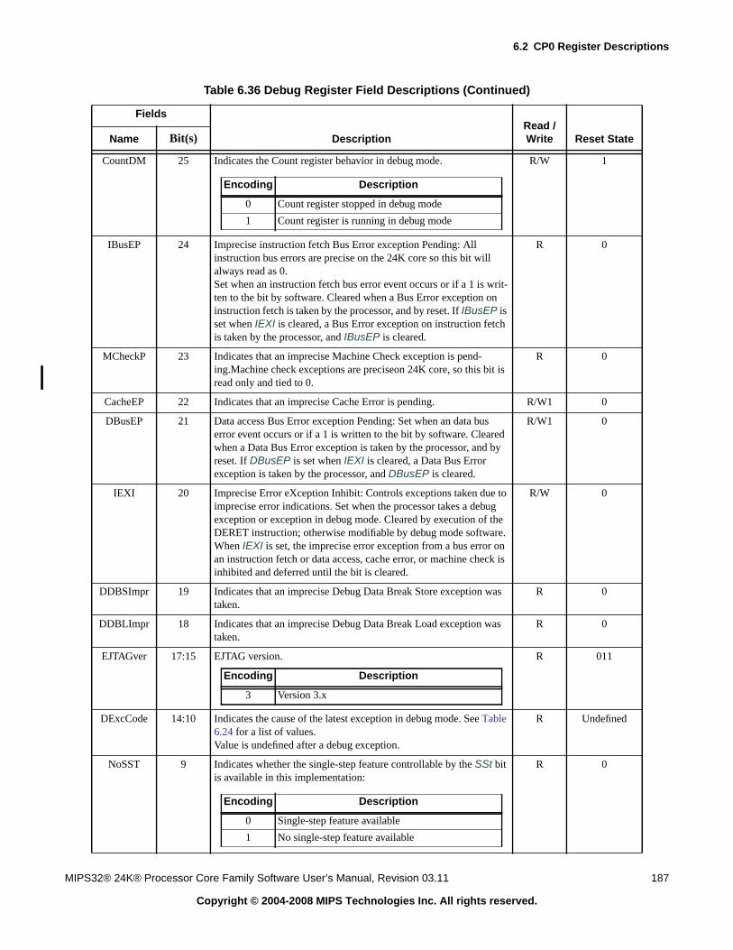
6.2 CP0 Register Descriptions
MIPS32® 24K® Processor Core Family Software User’s Manual, Revision 03.11 187
Copyright © 2004-2008 MIPS Technologies Inc. All rights reserved.
CountDM 25 Indicates the Count register behavior in debug mode. R/W 1
IBusEP 24 Imprecise instruction fetch Bus Error exception Pending: Allinstruction bus errors are precise on the 24K core so this bit willalways read as 0.Set when an instruction fetch bus error event occurs or if a 1 is writ-ten to the bit by software. Cleared when a Bus Error exception oninstruction fetch is taken by the processor, and by reset. If IBusEP isset when IEXI is cleared, a Bus Error exception on instruction fetchis taken by the processor, and IBusEP is cleared.
R 0
MCheckP 23 Indicates that an imprecise Machine Check exception is pend-ing.Machine check exceptions are preciseon 24K core, so this bit isread only and tied to 0.
R 0
CacheEP 22 Indicates that an imprecise Cache Error is pending. R/W1 0
DBusEP 21 Data access Bus Error exception Pending: Set when an data buserror event occurs or if a 1 is written to the bit by software. Clearedwhen a Data Bus Error exception is taken by the processor, and byreset. If DBusEP is set when IEXI is cleared, a Data Bus Errorexception is taken by the processor, and DBusEP is cleared.
R/W1 0
IEXI 20 Imprecise Error eXception Inhibit: Controls exceptions taken due toimprecise error indications. Set when the processor takes a debugexception or exception in debug mode. Cleared by execution of theDERET instruction; otherwise modifiable by debug mode software.When IEXI is set, the imprecise error exception from a bus error onan instruction fetch or data access, cache error, or machine check isinhibited and deferred until the bit is cleared.
R/W 0
DDBSImpr 19 Indicates that an imprecise Debug Data Break Store exception wastaken.
R 0
DDBLImpr 18 Indicates that an imprecise Debug Data Break Load exception wastaken.
R 0
EJTAGver 17:15 EJTAG version. R 011
DExcCode 14:10 Indicates the cause of the latest exception in debug mode. See Table6.24 for a list of values.Value is undefined after a debug exception.
R Undefined
NoSST 9 Indicates whether the single-step feature controllable by the SSt bitis available in this implementation:
R 0
Table 6.36 Debug Register Field Descriptions (Continued)
Fields
DescriptionRead /Write Reset StateName Bit(s)
Encoding Description
0 Count register stopped in debug mode
1 Count register is running in debug mode
Encoding Description
3 Version 3.x
Encoding Description
0 Single-step feature available
1 No single-step feature available

CP0 Registers of the 24K® Core
188 MIPS32® 24K® Processor Core Family Software User’s Manual, Revision 03.11
Copyright © 2004-2008 MIPS Technologies Inc. All rights reserved.
SSt 8 Controls if debug single step exception is enabled: R/W 0
R 7 Reserved. Must be written as zeros; returns zeros on reads. R 0
R 6 Reserved. Must be written as zeros; returns zeros on reads. R 0
DINT 5 Indicates that a debug interrupt exception occurred. Cleared onexception in debug mode.
R Undefined
DIB 4 Indicates that a debug instruction break exception occurred. Clearedon exception in debug mode.
R Undefined
DDBS 3 Indicates that a debug data break exception occurred on a store.Cleared on exception in debug mode.
R Undefined
DDBL 2 Indicates that a debug data break exception occurred on a load.Cleared on exception in debug mode.
R Undefined
DBp 1 Indicates that a debug software breakpoint exception occurred.Cleared on exception in debug mode.
R Undefined
Table 6.36 Debug Register Field Descriptions (Continued)
Fields
DescriptionRead /Write Reset StateName Bit(s)
Encoding Description
0 No debug single-step exception enabled
1 Debug single step exception enabled
Encoding Description
0 No debug interrupt exception
1 Debug interrupt exception
Encoding Description
0 No debug interrupt exception
1 Debug interrupt exception
Encoding Description
0 No debug data exception on a store
1 Debug instruction exception on a store
Encoding Description
0 No debug data exception on a load
1 Debug instruction exception on a load
Encoding Description
0 No debug software breakpoint exception
1 Debug software breakpoint exception

6.2 CP0 Register Descriptions
MIPS32® 24K® Processor Core Family Software User’s Manual, Revision 03.11 189
Copyright © 2004-2008 MIPS Technologies Inc. All rights reserved.
6.2.29 Trace Control Register (CP0 Register 23, Select 1)
The TraceControl register configuration is shown below.
Figure 6.30 TraceControl Register Format
DSS 0 Indicates that a debug single-step exception occurred. Cleared onexception in debug mode.
R Undefined
31 30 29 28 27 26 25 24 23 22 21 20 13 12 5 4 3 2 1 0
TS UT 0 TB IO D E K S U ASID_M ASID G TFCR TLSM TIM On
Table 6.37 TraceControl Register Field Descriptions
Fields
DescriptionRead /Write Reset StateName Bits
TS 31 The trace select bit is used to select between the hardware and thesoftware trace control bits. A value of zero selects the external hard-ware trace block signals, and a value of one selects the trace controlbits in the TraceControl register.
R/W 0
UT 30 This bit is used to indicate the type of user-triggered trace record. Avalue of zero implies a user type 1 and a value of one implies a usertype 2.The actual triggering of a user trace record happens on a write to theUserTraceData register. This is a 32-bit register for 32-bit proces-sors and a 64-bit register for 64-bit processors.
R/W Undefined
0 29:28 Reserved for future use; Must be written as zero; returns zero onread.
0 0
TB 27 Trace All Branch. When set to 1, this tells the processor to trace thePC value for all taken branches, not just the ones whose branch tar-get address is statically unpredictable.
R/W Undefined
IO 26 Inhibit Overflow. This signal is used to indicate to the core tracelogic that slow but complete tracing is desired. Hence, the core trac-ing logic must not allow a FIFO overflow and discard trace data.This is achieved by stalling the pipeline when the FIFO is nearlyfull, so that no trace records are ever lost.
R/W Undefined
Table 6.36 Debug Register Field Descriptions (Continued)
Fields
DescriptionRead /Write Reset StateName Bit(s)
Encoding Description
0 No debug single-step exception
1 Debug single-step exception

CP0 Registers of the 24K® Core
190 MIPS32® 24K® Processor Core Family Software User’s Manual, Revision 03.11
Copyright © 2004-2008 MIPS Technologies Inc. All rights reserved.
D 25 When set to one, this enables tracing in Debug Mode. For trace to beenabled in Debug mode, the On bit must be one, and either the G bitmust be one, or the current process ASID must match the ASID fieldin this register.When set to zero, trace is disabled in Debug Mode, irrespective ofother bits.
R/W Undefined
E 24 When set to one, this enables tracing in Exception Mode. For traceto be enabled in Exception mode, the On bit must be one, and eitherthe G bit must be one, or the current process ASID must match theASID field in this register.When set to zero, trace is disabled in Exception Mode, irrespectiveof other bits.
R/W Undefined
K 23 When set to one, this enables tracing in Kernel Mode. For trace to beenabled in Kernel mode, the On bit must be one, and either the G bitmust be one, or the current process ASID must match the ASID fieldin this register.When set to zero, trace is disabled in Kernel Mode, irrespective ofother bits.
R/W Undefined
S 22 When set to one, this enables tracing in Supervisor Mode.For traceto be enabled in Supervisor mode, the On bit must be one, and eitherthe G bit must be one, or the current process ASID must match theASID field in this register.When set to zero, trace is disabled in Supervisor Mode, irrespectiveof other bits.If the processor does not implement Supervisor Mode, this bit isignored on write and returns zero on read.
R/W Undefined
U 21 When set to one, this enables tracing in User Mode. For trace to beenabled in User mode, the On bit must be one, and either the G bitmust be one, or the current process ASID must match the ASID fieldin this register.When set to zero, trace is disabled in User Mode, irrespective ofother bits.
R/W Undefined
ASID_M 20:13 This is a mask value applied to the ASID comparison (done whenthe G bit is zero). A “1” in any bit in this field inhibits the corre-sponding ASID bit from participating in the match. As such, a valueof zero in this field compares all bits of ASID. Note that the abilityto mask the ASID value is not available in the hardware signal bit; itis only available via the software control register.If the processor does not implement the standard TLB-based MMU,this field is ignored on write and returns zero on read.
R/W Undefined
ASID 12:5 The ASID field to match when the G bit is zero. When the G bit isone, this field is ignored.If the processor does not implement the standard TLB-based MMU,this field is ignored on write and returns zero on read.
R/W Undefined
G 4 When set, this implies that tracing is to be enabled for all processes,provided that other enabling functions (like U, S, etc.,) are also true.If the processor does not implement the standard TLB-based MMU,this field is ignored on write and returns 1 on read. This causes allmatch equations to work correctly in the absence of an ASID.
R/W Undefined
Table 6.37 TraceControl Register Field Descriptions (Continued)
Fields
DescriptionRead /Write Reset StateName Bits

6.2 CP0 Register Descriptions
MIPS32® 24K® Processor Core Family Software User’s Manual, Revision 03.11 191
Copyright © 2004-2008 MIPS Technologies Inc. All rights reserved.
6.2.30 Trace Control2 Register (CP0 Register 23, Select 2)
The TraceControl2 register provides additional control and status information. Note that some fields in theTraceControl2 register are read-only, but have a reset state of “Undefined”. This is because these values are loadedfrom the Trace Control Block (TCB) (see Section 11.9 “Trace Control Block (TCB) Registers (Hardware Control)”).As such, these fields in the TraceControl2 register will not have valid values until the TCB asserts these values.
This register is only implemented if the MIPS Trace capability is present.
Figure 6.31 TraceControl2 Register Format
TFCR 3 When asserted, used to trace function call and return instructionswith full PC values.
R/W Undefined
TLSM 2 When asserted, used to trace data cache load and store misses withfull PC values, and potentially the data address and value as well.
R/W Undefined
TIM 1 When asserted, used to trace instruction miss with full PC values. R/W Undefined
On 0 This is the master trace enable switch in software control. Whenzero, tracing is always disabled. When set to one, tracing is enabledwhenever the other enabling functions are also true.
R/W 0
31 30 29 28 21 20 19 12 11 7 6 5 4 3 2
0 CPUIdV CPUId TCV TCNum Mode ValidModes TBI TBU SyP
Table 6.38 TraceControl2 Register Field Descriptions
Fields
DescriptionRead /Write Reset StateName Bits
0 31:30 Reserved for future use; Must be written as zero; returns zero onread.
0 0
CPUIdV,CPUId,TCV,
TCNum
29:12 Used on processors implementing the MT ASE R 0
Table 6.37 TraceControl Register Field Descriptions (Continued)
Fields
DescriptionRead /Write Reset StateName Bits

CP0 Registers of the 24K® Core
192 MIPS32® 24K® Processor Core Family Software User’s Manual, Revision 03.11
Copyright © 2004-2008 MIPS Technologies Inc. All rights reserved.
Mode 11:7 These 5 bits provide the same trace mode functions as thePDI_TraceMode[4:0] signal, and is described here again.When tracing is turned on, this signal specifies what information isto be traced by the core. It uses 5 bits, where each bit turns on trac-ing of a specific tracing mode when that bit value is a 1. If the corre-sponding bit is 0, then the Trace Value shown in column two is nottraced by the processor.On the 24K core, PC tracing is always enabled, regardless of thevalue on bit 7. The table shows what trace value is turned on:
R/W Undefined
Valid-Modes
6:5 This field specifies the subset of tracing that is supported by the pro-cessor.
R Preset
TBI 4 This bit indicates how many trace buffers are implemented by theTCB, as follows:
This bit is loaded from the PDI_TBImpl signal when thePDI_SyncOffEn signal is asserted.
R Undefined
TBU 3 This bit denotes to which trace buffer the trace is currently beingwritten and is used to select the appropriate interpretation of theTraceControl2SyP field.
This bit is loaded from the PDI_OffChipTB signal when thePDI_SyncOffEn signal is asserted.
R Undefined
Table 6.38 TraceControl2 Register Field Descriptions
Fields
DescriptionRead /Write Reset StateName Bits
Bit Trace the Following
7 PC
8 Load address
9 Store address
10 Load data
11 Store data
Encoding Meaning
00 PC tracing only
01 PC and load and store address tracing only
10 PC, load and store address, and load and store data
11 Reserved
Encoding Meaning
0 Only one trace buffer is implemented, and the TBUbit of this register indicates which trace buffer isimplemented
1 Both on-chip and off-chip trace buffers are imple-mented by the TCB and the TBU bit of this registerindicates to which trace buffer the traces is cur-rently written.
Encoding Meaning
0 Trace data is being sent to an on-chip trace buffer
1 Trace Data is being sent to an off-chip trace buffer

6.2 CP0 Register Descriptions
MIPS32® 24K® Processor Core Family Software User’s Manual, Revision 03.11 193
Copyright © 2004-2008 MIPS Technologies Inc. All rights reserved.
6.2.31 User Trace Data Register (CP0 Register 23, Select 3)
A software write to any bits in the UserTraceData register will trigger a trace record to be written indicating a type 1or type 2 user format. The type is based on the UT bit in the TraceControl register. This register cannot be written inconsecutive cycles. The trace output data is UNPREDICTABLE if this register is written in consecutive cycles.
This register is only implemented if the MIPS Trace capability is present.
Figure 6.32 User Trace Data Register Format
6.2.32 TraceIBPC Register (CP0 Register 23, Select 4)
The TraceIBPC register is used to control start and stop of tracing using an EJTAG Instruction Hardware breakpoint.The Instruction Hardware breakpoint would then be set as a trigger source and optionally also as a Debug exceptionbreakpoint.
SyP 2:0 The period (in cycles) to which the internal synchronization counteris reset when tracing is started, or when the synchronization counterhas overflowed.
This field is loaded from the PDI_SyncPeriod signal when thePDI_SyncOffEn signal is asserted.
R Undefined
31 0
Data
Table 6.39 UserTraceData Register Field Descriptions
Fields
DescriptionRead /Write Reset StateName Bits
Data 31:0 Software readable/writable data. When written, this triggers a userformat trace record out of the PDtrace interface that transmits theData field to trace memory.
R/W 0
Table 6.38 TraceControl2 Register Field Descriptions
Fields
DescriptionRead /Write Reset StateName Bits
SyP Sync Period
000 25
001 26
010 27
011 28
100 29
101 210
110 211
111 212

CP0 Registers of the 24K® Core
194 MIPS32® 24K® Processor Core Family Software User’s Manual, Revision 03.11
Copyright © 2004-2008 MIPS Technologies Inc. All rights reserved.
This register is only implemented if both Hardware breakpoints and the MIPS Trace capability are present.
Figure 6.33 TraceIBPC Register Format
6.2.33 TraceDBPC Register (CP0 Register 23, Select 5)
The TraceDBPC register is used to control start and stop of tracing using an EJTAG Data Hardware breakpoint. TheData Hardware breakpoint would then be set as a trigger source and optionally also as a Debug exception breakpoint.
This register is only implemented if both Hardware breakpoints and the MIPS Trace capability are present.
Figure 6.34 TraceDBPC Register Format
31 29 28 27 12 11 9 8 6 5 3 2 0
0 IE 0 IBPC3 IBPC2 IBPC1 IBPC0
Table 6.40 TraceIBPC Register Field Descriptions
Fields
DescriptionRead /Write Reset StateName Bits
0 31:29,27:12
Reserved for future implementation. R 0/1
IE 28 Used to specify whether the trigger signal from EJTAG instructionbreakpoint should trigger tracing functions or not:
R/W 0
IBPCn 3n+2:3n The three bits are decoded to enable different tracing modes. Table6.42 shows the possible interpretations. Each set of 3 bits representsthe encoding for the instruction breakpoint n in the EJTAG imple-mentation, if it exists. If the breakpoint does not exist, then the bitsare reserved, read as zero, and writes are ignored.
R/W 0
31 29 28 27 6 5 3 2 0
0 DE 0 DBPC1 DBPC0
Table 6.41 TraceDBPC Register Field Descriptions
Fields
DescriptionRead /Write Reset StateName Bits
0 31:29,27:6
Reserved for future implementation R 0/1
Encoding Meaning
0 Disables trigger signals from instruction break-points
1 Enables trigger signals from instruction break-points

6.2 CP0 Register Descriptions
MIPS32® 24K® Processor Core Family Software User’s Manual, Revision 03.11 195
Copyright © 2004-2008 MIPS Technologies Inc. All rights reserved.
6.2.34 Debug Exception Program Counter Register (CP0 Register 24, Select 0)
The Debug Exception Program Counter (DEPC) register is a read/write register that contains the address at whichprocessing resumes after a debug exception or debug mode exception has been serviced.
For synchronous (precise) debug and debug mode exceptions, the DEPC contains either:
• The virtual address of the instruction that was the direct cause of the debug exception, or
• The virtual address of the immediately preceding branch or jump instruction, when the debug exception causinginstruction is in a branch delay slot, and the Debug Branch Delay (DBD) bit in the Debug register is set.
For asynchronous debug exceptions (debug interrupt), the DEPC contains the virtual address of the instruction whereexecution should resume after the debug handler code is executed.
In processors that implement the MIPS16 ASE, a read of the DEPC register (via MFC0) returns the following valuein the destination GPR:
GPR[rt] ← DebugExceptionPC31..1 || ISAMode0
That is, the upper 31 bits of the debug exception PC are combined with the lower bit of the ISAMode field and writtento the GPR.
DE 28 Used to specify whether the trigger signal from EJTAG data break-point should trigger tracing functions or not:
R/W 0
DBPCn 3n+2:3n The three bits are decoded to enable different tracing modes. Table6.42 shows the possible interpretations. Each set of 3 bits representsthe encoding for the data breakpoint n in the EJTAG implementa-tion, if it exists. If the breakpoint does not exist then the bits arereserved, read as zero and writes are ignored.
R/W 0
Table 6.42 BreakPoint Control Modes: IBPC and DBPC
Value Trigger Action Description
000 Unconditional Trace Stop Unconditionally stop tracing if tracing was turned on. If tracing isalready off, then there is no effect.
001 Unconditional Trace Start Unconditionally start tracing if tracing was turned off. If tracing isalready turned on, then there is no effect.
010 to 111 Not used Reserved for future implementation
Table 6.41 TraceDBPC Register Field Descriptions
Fields
DescriptionRead /Write Reset StateName Bits
Encoding Meaning
0 Disables trigger signals from data breakpoints
1 Enables trigger signals from data breakpoints

CP0 Registers of the 24K® Core
196 MIPS32® 24K® Processor Core Family Software User’s Manual, Revision 03.11
Copyright © 2004-2008 MIPS Technologies Inc. All rights reserved.
Similarly, a write to the DEPC register (via MTC0) takes the value from the GPR and distributes that value to thedebug exception PC and the ISA Mode field, as follows
DebugExceptionPC ← GPR[rt]31..1 || 0ISAMode ← 2#0 || GPR[rt]0
That is, the upper 31 bits of the GPR are written to the upper 31 bits of the debug exception PC, and the lower bit ofthe debug exception PC is cleared. The upper bit of the ISAMode field is cleared and the lower bit is loaded from thelower bit of the GPR.
Figure 6.35 DEPC Register Format
6.2.35 Performance Counter Register (CP0 Register 25, select 0-3)
The 24K processor defines two performance counters and two associated control registers, which are mapped to CP0register 25. The select field of the MTC0/MFC0 instructions are used to select the specific register accessed by theinstruction, as shown in Table 6.44.
Each counter is a 32-bit read/write register and is incremented by one each time the countable event, specified in itsassociated control register, occurs. Each counter can independently count one type of event at a time.
Bit 31 of each of the counters are AND’ed with an interrupt enable bit, IE, of their respective control register to deter-mine if a performance counter interrupt should be signalled. The two values are then OR’ed together to create theSI_PCI output. This signal is combined with one of the SI_Int pins to signal an interrupt to the core. Counting is notaffected by the interrupt indication. This output is cleared when the counter wraps to zero, and may be cleared in soft-ware by writing a value with bit 31 = 0 to the Performance Counter Count registers.
31 0
DEPC
Table 6.43 DEPC Register Formats
Fields
DescriptionRead /Write ResetName Bit(s)
DEPC 31:0 The DEPC register is updated with the virtual address of the instruc-tion that caused the debug exception. If the instruction is in thebranch delay slot, then the virtual address of the immediately pre-ceding branch or jump instruction is placed in this register.Execution of the DERET instruction causes a jump to the address inthe DEPC.
R/W Undefined
Table 6.44 Performance Counter Register Selects
Select[2:0] Register
0 Register 0 Control
1 Register 0 Count
2 Register 1 Control
3 Register 1 Count

6.2 CP0 Register Descriptions
MIPS32® 24K® Processor Core Family Software User’s Manual, Revision 03.11 197
Copyright © 2004-2008 MIPS Technologies Inc. All rights reserved.
NOTE: the performance counter registers are connected to a clock that is stopped when the processor is in sleep mode(if the top level clock gater is present). Most events would not be active during that time, but others would be, notablythe cycle count. This behavior should be considered when analyzing measurements taken on a system. Further, notethat FPGA implementations of the core would generally not have the clock gater present and thus would have differ-ent behavior than a typical ASIC implementation.
For a more detailed description of performance counter events, refer to Programming the 24K Core Family [7].
Figure 6.36 Performance Counter Control Register
Table 6.46 describes the events countable with the two performance counters. The mode column indicates whetherthe event counting is influenced by the mode bits (U,S,K,EXL) The operation of a counter is UNPREDICTABLE forevents which are specified as Reserved. The performance counter resets to a low-power state, in which none of the
31 12 11 5 4 3 2 1 0
M 0 Event IE U S K EXL
Table 6.45 Performance Counter Control Register Field Descriptions
Fields
DescriptionRead/Write Reset StateName Bits
M 31 If this bit is one, another pair of Performance Control and Counterregisters is implemented at a MTC0 or MFC0 select field value of‘n+2’ and ‘n+3’.
R Preset
Event 11:5 Counter event enabled for this counter. Possible events are listed inTable 6.46.
R/W Undefined
IE 4 Counter Interrupt Enable. This bit masks bit 31 of the associatedcount register from the interrupt exception request output.
R/W 0
U 3 Count in User Mode. When this bit is set, the specified event iscounted in User Mode.
R/W Undefined
S 2 Count in Supervisor Mode. When this bit is set, the specified eventis counted in Supervisor Mode.
R/W Undefined
K 1 Count in Kernel Mode. When this bit is set, count the event in Ker-nel Mode when EXL and ERL both are 0.
R/W Undefined
EXL 0 Count when EXL. When this bit is set, count the event when EXL =1 and ERL = 0.
R/W Undefined
0 30, 15:12 Must be written as zeroes; returns zeroes when read. 0 0
Table 6.46 Performance Counter Count Register Field Descriptions
Event Num Counter 0 Mode Counter 1 Mode
0 Cycles No Cycles No
1 Instructions completed Yes Instructions completed Yes
2 branch instructions Yes Branch mispredictions Yes
3 JR r31 (return) instructions Yes JR r31 mispredictions Yes
4 JR (not r31) instructions Yes JR r31 not predicted Yes

CP0 Registers of the 24K® Core
198 MIPS32® 24K® Processor Core Family Software User’s Manual, Revision 03.11
Copyright © 2004-2008 MIPS Technologies Inc. All rights reserved.
5 ITLB accesses Yes ITLB misses Yes
6 DTLB accesses Yes DTLB misses Yes
7 JTLB instruction accesses Yes JTLB instruction misses Yes
8 JTLB data accesses Yes JTLB data misses Yes
9 Instruction Cache accesses Yes Instruction cache misses Yes
10 Data cache accesses Yes Data cache writebacks Yes
11 Data cache misses Yes Data cache misses Yes
12 Reserved Yes Reserved Yes
13 Store Misses Yes Load Misses Yes
14 integer instructions completed Yes FPU instructions completed Yes
15 loads completed Yes stores completed Yes
16 J/JAL completed Yes MIPS16 instructions completed Yes
17 no-ops completed Yes integer multiply/divide completed Yes
18 Stall cycles No replay traps (other than uTLB) Yes
19 SC instructions completed Yes SC instructions failed Yes
20 Prefetch instructions completed Yes Prefetch instructions completed with cachehit
Yes
21 L2 cache writebacks No L2 cache accesses No
22 L2 cache misses No L2 cache single bit errors corrected No
23 Exceptions taken Yes Reserved Yes
24 cache fixup Yes Reserved Yes
25 IFU stall cycles No ALU stall cycles No
26 Reserved Yes Reserved Yes
27 Reserved Yes Reserved Yes
28 Reserved Yes Impl. specific Cp2 event Yes
29 Impl. specific ISPRAM event Yes Impl. specific DSPRAM event Yes
30 Impl. specific CorExtend event Yes Reserved Yes
31 Reserved Yes Reserved Yes
32 Reserved Yes Reserved Yes
33 Uncached Loads Yes Uncached Stores Yes
34 Reserved Yes Reserved Yes
35 CP2 Arithmetic Instns Completed No CP2 To/From Instns completed Yes
Table 6.46 Performance Counter Count Register Field Descriptions
Event Num Counter 0 Mode Counter 1 Mode

6.2 CP0 Register Descriptions
MIPS32® 24K® Processor Core Family Software User’s Manual, Revision 03.11 199
Copyright © 2004-2008 MIPS Technologies Inc. All rights reserved.
36 Reserved
37 I$ Miss stall cycles Yes D$ miss stall cycles Yes
38 SYNC stalls Yes FSB Index Conflicts Yes
39 D$ miss cycles No L2 miss cycles No
40 Uncached stall cycles Yes Reserved Yes
41 MDU stall cycles Yes FPU stall cycles Yes
42 CP2 stall cycles Yes CorExtend stall cycles Yes
43 ISPRAM stall cycles Yes DSPRAM stall cycles Yes
44 CACHE Instn stall cycles No Reserved Yes
45 Load to Use stall cycles Yes ALU to AGEN stall cycles Yes
46 Other interlock stall cycles Yes Branch mispredict stall cycles No
47 Reserved Yes Reserved Yes
48 IFU FB full refetches Yes FB entry allocated No
49 EJTAG Instruction Triggerpoints Yes EJTAG Data Triggerpoints Yes
50 FSB < 1/4 full No FSB 1/4-1/2 full No
51 FSB > 1/2 full No FSB full pipeline stall cycles No
52 LDQ < 1/4 full No LDQ 1/4-1/2 full No
53 LDQ > 1/2 full No LDQ full pipeline stall cycles No
54 WBB < 1/4 full No WBB 1/4-1/2 full No
55 WBB > 1/2 full No WBB full pipeline stall cycles No
56-63 Reserved
64 SI_PCEvent[0] - System specific event 0 No SI_PCEvent[1] - System specific event 1 No
65 SI_PCEvent[2] - System specific event 2 No SI_PCEvent[3] - System specific event 3 No
66 SI_PCEvent[4] - System specific event 4 No SI_PCEvent[5] - System specific event 5 No
67 SI_PCEvent[6] - System specific event 6 No SI_PCEvent[7] - System specific event 7 No
68-127 Reserved
56-63 Reserved
Table 6.46 Performance Counter Count Register Field Descriptions
Event Num Counter 0 Mode Counter 1 Mode

CP0 Registers of the 24K® Core
200 MIPS32® 24K® Processor Core Family Software User’s Manual, Revision 03.11
Copyright © 2004-2008 MIPS Technologies Inc. All rights reserved.
Table 6.47 Event Descriptions
Event Name CounterEvent
Number Description
Cycles 0/1 0 Total number of cycles.The performance counters are clocked by the top-level gated clock. Ifthe core is built with that clock gater present, none of the counters willincrement while the clock is stopped - due to a WAIT instruction.
Instruction Completion: The following events indicate completion of various types of instructions
Instructions 0/1 1 Total number of instructions completed.
Branch instns 0 2 Counts all branch instructions that completed.
JR R31 (return) instns 0 3 Counts all JR R31 instructions that completed.
JR (not R31) 0 4 Counts all JR $xx (not $31) and JALR instructions (indirect jumps).
Integer instns 0 14 Non-floating point, non-Coprocessor 2 instructions.
FPU instns 1 14 Floating point instructions.
Loads 0 15 Includes both integer and coprocessor loads.
Stores 1 15 Includes both integer and coprocessor stores.
J/JAL 0 16 Direct Jump (And Link) instruction.
MIPS16e 1 16 All MIPS16e instruction.
no-ops 0 17 This includes all instructions that normally write to a GPR, but wherethe destination register was set to r0.
Integer Multiply/Divide 1 17 Counts all Integer Multiply/Divide instructions (MULxx, DIVx,MADDx, MSUBx).
SC 0 19 Counts conditional stores regardless of whether they succeeded.
PREF 0 20 Note that this only counts PREFs that are actually attempted. PREFsto uncached addresses or ones with translation errors are not counted
Uncached Loads 0 33 Include both Uncached and Uncached Accelerated CCAs.
Uncached Stores 1 33
Cp2 Arithmetic instns 0 35 Counts Coprocessor 2 register-to-register instructions.
Cp2 To/From instns 1 35 Includes move to/from, control to/from, and cop2 loads and stores.
Instruction execution events
Branch mispredicts 1 2 Counts all branch instructions which completed, but were mispre-dicted.
JR r31 mispredicts 1 3 Counts all JR $31 instructions which completed, used the RPS for aprediction, but were mispredicted.
JR r31 not-predicted 1 4 If RPS use is disabled, JR $31 will not be predicted.
ITLB accesses 0 5 Counts ITLB accesses that are due to fetches showing up in IF stage ofthe pipe and do not use fixed mapping or are not in unmapped space.If an address is fetched twice down the pipe (as in the case of a cachemiss), that instruction will count 2 ITLB accesses. Also, since eachfetch gets us 2 instructions, there is one access marked per doubleword.

6.2 CP0 Register Descriptions
MIPS32® 24K® Processor Core Family Software User’s Manual, Revision 03.11 201
Copyright © 2004-2008 MIPS Technologies Inc. All rights reserved.
ITLB misses 1 5 Counts all misses in ITLB except ones that are on the back of anothermiss. We cannot process back to back misses and thus those areignored for this purpose. Also ignored if there is some form of addresserror.
DTLB accesses 0 6 Counts DTLB access including those in unmapped address spaces.
DTLB misses 1 6 Counts DTLB misses. Back to back misses that result in only oneDTLB entry getting refilled are counted as a single miss.
JTLB instruction accesses 0 7 Instruction JTLB accesses are counted exactly the same as ITLBmisses.
JTLB instruction misses 1 7 Counts instruction JTLB accesses that result in no match or a matchon an invalid translation.
JTLB data accesses 0 8 Data JTLB accesses.
JTLB data misses 1 8 Counts data JTLB accesses that result in no match or a match on aninvalid translation.
I$ accesses 0 9 Counts every time the instruction cache is accessed. All replays,wasted fetches etc. are counted. For example, following a branch,even the prediction is taken, the fall through access is counted.
I$ misses 1 9 Counts all instruction cache misses that result in a bus request.
D$ accesses 0 10 Counts cached loads and stores.
D$ writebacks 1 10 Counts cache lines written back to memory due to replacement orcacheops.
D$ misses 0/1 11 Counts loads and stores that miss in the cache
Load Misses 0 13 Counts number of cacheable loads that miss in the cache.
Store Misses 1 13 Counts number of cacheable stores that miss in the cache.
SC instructons failed 1 19 SC instruction that did not update memoryNote: While this event and the SC instruction count event can be con-figured to count in specific operating modes, the timing of the eventsis much different and the observed operating mode could changebetween them, causing some inaccuracy in the measured ratio.
PREF completed with cache hit 1 20 Counts PREF instructions that hit in the cache
L2 Cache Writebacks 0 21 Counts cache lines written back to memory due to replacement orcacheops
L2 Cache Accesses 1 21 Number of accesses to L2 Cache
L2 Cache Misses 0 22 Number of accesses that missed in the L2 cache
L2 Cache Single Bit Errors Corrected 1 22 Single bit errors in L2 Cache that were detected and corrected
Exceptions Taken 0 23 Any type of exception taken
EJTAG instruction triggers 0 49 Number of times an EJTAG Instruction Trigger Point conditionmatched
EJTAG data triggers 1 49 Number of times an EJTAG Data Trigger Point condition matched
Pipeline Fun
Table 6.47 Event Descriptions (Continued)
Event Name CounterEvent
Number Description

CP0 Registers of the 24K® Core
202 MIPS32® 24K® Processor Core Family Software User’s Manual, Revision 03.11
Copyright © 2004-2008 MIPS Technologies Inc. All rights reserved.
Cache fixup 0 24 Counts cycles where the LSU is in fixup and cannot accept a newinstruction from the ALU. Fixups are replays within the LSU thatoccur when an instruction needs to re-access the cache or the DTLB
General Stalls
IFU stall cycles 0 25 Counts the number of cycles where the fetch unit is not providing avalid instruction to the ALU.
ALU stall cycles 1 25 Counts the number of cycles where the ALU pipeline cannot advance.
Stall cycles 0 18 Counts the total number of cycles where no instructions are issued byIFU to ALU (the RF stage does not advance). This includes both ofthe previous two events. This is different than the sum of them thoughbecause cycles when both stalls are active will only be counted once.
Specific stalls - these events will count the number of cycles lost due to this. This will include bubbles introduced by replays within thepipe. If multiple stall sources are active simultaneously, the counters for each of the active events will be incremented.
SYNC stall cycles 0 38 Cycles where the main pipeline is stalled waiting for a SYNC to com-plete
FSB index conflict stall cycles 1 38 Cycles where the main pipeline is stalled because of an index conflictin the Fill Store Buffer.
I$ miss stall cycles 0 37 Cycles when IFU stalls because an I$ miss caused the IFU not to haveany runnable instructions. Ignores the stalls due to ITLB misses aswell as the 4 cycles following a redirect.
D$ miss stall cycles 1 37 Counts all cycles where integer pipeline waits on Load return data dueto a D-cache miss. The LSU can signal a “long stall” on a D-cachemisses, in which case the waiting TC might be rescheduled so otherTCs can execute instructions till the data returns.
D$ miss cycle cycles 0 39 D$ miss is outstanding, but not necessarily stalling the pipeline. Thedifference between this and D$ miss stall cycles can show the gainfrom non-blocking cache misses.
L2 miss cycles 1 39 L2 miss is outstanding, but not necessarily stalling the pipeline.
Uncached stall cycles 0 40 Cycles where the processor is stalled on an uncached fetch, load, orstore.
MDU stall cycles 0 41 Counts all cycles where integer pipeline waits on MDU return data.
FPU stall cycles 1 41 Counts all cycles where integer pipeline waits on FPU return data.
Cp2 stall cycles 0 42 Counts all cycles where integer pipeline waits on CP2 return data.
CorExtend stall cycles 1 42 Counts all cycles where integer pipeline waits on CorExtend returndata.
ISPRAM stall cycles 0 43 Count all pipeline bubbles that are a result of multicycle ISPRAMaccess. Pipeline bubbles are defined as all cycles that IFU doesn’tpresent an instruction to ALU. The four cycles after a redirect are notcounted.
DSPRAM stall cycles 1 43 Counts stall cycles created by an instruction waiting for access toDSPRAM.
Table 6.47 Event Descriptions (Continued)
Event Name CounterEvent
Number Description

6.2 CP0 Register Descriptions
MIPS32® 24K® Processor Core Family Software User’s Manual, Revision 03.11 203
Copyright © 2004-2008 MIPS Technologies Inc. All rights reserved.
CACHE instn stall cycles 0 44 Counts all cycles where pipeline is stalled due to CACHE instructions.Includes cycles where CACHE instructions themselves are stalled inthe ALU, and cycles where CACHE instructions cause subsequentinstructions to be stalled.
Load to Use stall cycles 0 45 Counts all cycles where integer pipeline waits on Load return data.
ALU to AGEN stall cycles 1 45 Counts stall cycles due to skewed ALU where the bypass to theaddress generation takes an extra cycle.
Other interlocks stall cycles 0 46 Counts all cycles where integer pipeline waits on return data fromMFC0, RDHWR instructions.
Branch mispredict stalls cycles 1 46 This counts the number of cycles from a mispredicted branch until thenext non-delay slot instruction executes.
FSB full pipeline stall cycles 1 51 Cycles where the pipeline is stalled because the Fill-Store Buffer inLSU is full.
LDQ full pipeline stall cycles 1 53 Cycles where the pipeline is stalled because the Load Data Queue inthe LSU is full.
Write Back Buffer full stall cycles 1 55 Cycles where the pipeline is stalled because the WriteBack Buffer inthe BIU is full.
Latency Events - These events provide a statistical sampling of latencies within the system. One particular FSB entry is monitored. Thelatency event increments each cycle from the time a request is generated until response is seen. The count events are incremented once foreach request that we are counting the latency for.
Request Latency to Read Response 0 61 Measures latency from miss detection until critical dword of responseis returned, Only counts for cacheable reads.
Request Count for RR Latency 1 61 Counts number of cacheable read requests used for previous latencycounter.
Implementation specific events - Modules that can be replaced by the customer will have an event signal associated with them.
Cp2 1 28
ISPRAM 0 29
DSPRAM 1 29
CorExtend 0 30
SI_PCEvent[7:0] 0/1 64-67
Buffer usage events - These count the number of cycles that buffers within the core spend at various levels of fullness.
Fill Store Buffer < 1/4 full 0 50 Buffer Occupancy:The following table shows what values fall into each of the bins forthe different buffer sizes that can be chosen.Fill Store Buffer 1/4 to 1/2 full 1 50
Fill Store Buffer > 1/2 full 0 51
Load Data Queue < 1/4 full 0 52
Load Data Queue 1/4 to 1/2 full 1 52
Load Data Queue > 1/2 full 0 53
Write Back Buffer < 1/4 full 0 54
Write Back Buffer 1/4 to 1/2 full 1 54
Write Back Buffer > 1/2 full 0 55
Table 6.47 Event Descriptions (Continued)
Event Name CounterEvent
Number Description
State 4 Entry Buffer 8/9 Entry Buffer
< 1/4 0 0-1
1/4-1/2 1-2 2-4
> 1/2 3+ 5+

CP0 Registers of the 24K® Core
204 MIPS32® 24K® Processor Core Family Software User’s Manual, Revision 03.11
Copyright © 2004-2008 MIPS Technologies Inc. All rights reserved.
counters will start counting events until software has enabled event counting, using an MTC0 instruction to the Per-formance Counter Control Registers.
Figure 6.37 Performance Counter Count Register
6.2.36 ErrCtl Register (CP0 Register 26, Select 0)
The ErrCtl register controls parity protection of data and instruction caches and provides for software testing of theway-selection and scratchpad RAMs.
Parity protection can be enabled or disabled using the PE bit. When parity is enabled and the PO bit is deasserted, theCACHE Index Store Tag and Index Store Data operations will internally generate parity to be written into the RAMarrays. However, when the PO bit is asserted, tag array parity is written using the P bit of the TagLo register and dataarray parity is written using the PI/PD bits of ErrCtl.
ECC protection for the secondary cache is controlled by a combination of PE and the L2P bits.
A CACHE Index Load Tag operation to the instruction cache will update the PCI field with the instruction precodebits from the data array and the PI field with the parity bits from the data array if parity is supported. A CACHE IndexLoad Tag operation to the data cache will cause the PD bits to be updated with the byte parity for the selected word ofthe data array if parity is implemented. If parity is disabled or not implemented, the contents of the PI and PD fieldsafter a CACHE Index Load Tag operation will be 0.
The PCO field can be used for testing the precode bits of the instruction cache data array. When the PCO bit iscleared, the CACHE Index Store Data instruction will internally generate the precode bits to be written into theinstruction cache data array. However, when the PCO bit is set, the CACHE Index Store Data instruction will writethe value in the PCI field to the precode bits in the data array. Setting an illegal value in the precode bits will causeunpredictable behavior. This mechanism should only be used for software testing of the cache arrays. Furthermore,the cache should be flushed after testing.
The way- selection RAM test mode is enabled by setting the WST bit. This mode is intended for software testing ofthe way-selection RAM and data RAM. It modifies the functionality of the CACHE Index Load Tag and Index Store
IFU Fill buffer allocated 1 48 Number of cycles where at least one of the IFU fill buffers is allocated(miss pending)
Refetches due to all IFU Fill Buff-ers allocated
0 48 Counts the number of times an instruction cache miss was detected,but both fill buffers were already allocated.
31 0
Counter
Table 6.48 Performance Counter Count Register Field Descriptions
Fields
DescriptionRead /Write Reset StateName Bits
Counter 31:0 Counter R/W Undefined
Table 6.47 Event Descriptions (Continued)
Event Name CounterEvent
Number Description

6.2 CP0 Register Descriptions
MIPS32® 24K® Processor Core Family Software User’s Manual, Revision 03.11 205
Copyright © 2004-2008 MIPS Technologies Inc. All rights reserved.
Tag operations so that they modify the way-selection RAM instead of the TAG RAMs. In addition, when the WST bitis set, the CACHE Index Store Data can be used for testing the data RAM.
Setting the SPR bit enables scratchpad test mode. This mode allows reading and writing of the scratchpad pseudo-tags as well the scratchpad data array.
At most one of the WST and SPR bits should be set. Setting multiple bits will lead to unpredictable behavior. Refer to“CACHE” on page 329 for a description of CACHE instruction operation for the different values of these bits.
Figure 6.38 ErrCtl Register31 30 29 28 27 26 25 24 23 22 21 20 19 18 13 12 4 3 0
PE PO WST SPR PCO 0 LBE WABE L2P 0 SE FE PCI PI PD
Table 6.49 ErrCtl Register Field Descriptions
Fields
DescriptionRead /Write Reset StateName Bits
PE 31 Parity Enable. This bit enables or disables the cache parity protec-tion for both the instruction cache and the data cache.
This field is only write-able if the cache parity option was imple-mented when the core was built. If cache parity is not supported, thisfield is always read as 0. Software can test for cache parity supportby attempting to write a 1 to this field, then read back the value.
R or R/W 0
PO 30 Parity Overwrite. If set, the PI/PD fields of this register overwritescalculated parity for the data array. In addition, the P field of theTagLo register overwrites calculated parity for the tag array. Thisbit only has significance during CACHE Index Store Tag andCACHE Index Store Data operations.
R/W 0
WST 29 Way Selection Test. If set, way-selection RAM test mode is enabled.This affects only the CACHE instruction operation. CACHE instruc-tion behavior is undefined if this bit is set at the same time as SPR.
R/W 0
SPR 28 ScratchPadRAM test. If set, indexed CACHE instructions operateon the ScratchPad RAM. Undefined behavior if ScratchPad RAM isnot present or if this bit is set at the same time as WST.
R/W 0
Encoding Meaning
0 Parity disabled
1 Parity enabled
Encoding Meaning
0 Use calculated parity
1 Override calculated parity
Encoding Meaning
0 Test mode disabled
1 Test mode enabled

CP0 Registers of the 24K® Core
206 MIPS32® 24K® Processor Core Family Software User’s Manual, Revision 03.11
Copyright © 2004-2008 MIPS Technologies Inc. All rights reserved.
PCO 27 Precode override. If set, the contents of the PCI field overwrite thecalculated precode bits when data is written to the instruction cachefor CACHE IndexStoreData operations.
R/W 0
ITC 26 InterThread Communication. If set, Index Load Tag and Index StoreTag CACHE instructions operate on the ITC tag.CACHE instruction behavior is undefined if this bit is set at thesame time as WST or SPR.
R/W 0
LBE 25 Bit indicating that the most recent Data Bus Error was involved aload instruction. A Per-TC BE bit will indicate which TCs wereimpacted.
R Undefined
WABE 24 Bit indicating that the most recent Data Bus Error was due to a writeallocate and that store data was lost. There is no indication of whichTC(s) the store request came from.It is possible for both LBE and WABE to be set if the bus error wason a line being used for both loads and stores.
R Undefined
L2P 23 L2 ECC Enable. This bit can be set only if the L2 is ECC-capable.This bit in conjunction with the PE bit enables or disables the ECCprotection for the L2 cache:
R/W 0
0 26,22:21 Must be written as zeroes; returns zeroes when read. 0 0
SE 20 Indicates that a second cache error was detected before the first errorwas processed. This is an unrecoverable error. This bit is set when acache error is detected while the FE bit is set. This bit is cleared onreset or when a cache error is detected with FE cleared.
R 0
FE 19 Indicates that this is the first cache error and therefore potentiallyrecoverable. Error handling software should clear this bit when theerror has been processed. This bit is cleared on reset. Refer to SE bitdescription for implications of this bit.
R/W 0
PCI 18:13 Instruction precode bits read from or written to the instruction cachedata RAM.
R/W Undefined
PI 12:4 Parity bit read from or written to instruction cache data RAM. R/W Undefined
Table 6.49 ErrCtl Register Field Descriptions
Fields
DescriptionRead /Write Reset StateName Bits
Encoding Meaning
0 Use calculated precode
1 Override calculated precode
PE L2P L2 check
1 0 1
1 1 0
0 0 0
0 1 1
Bits Meaning
12 Even parity bit for the pre-code bits
11:4 Per-byte even parity bits for the 64b of data
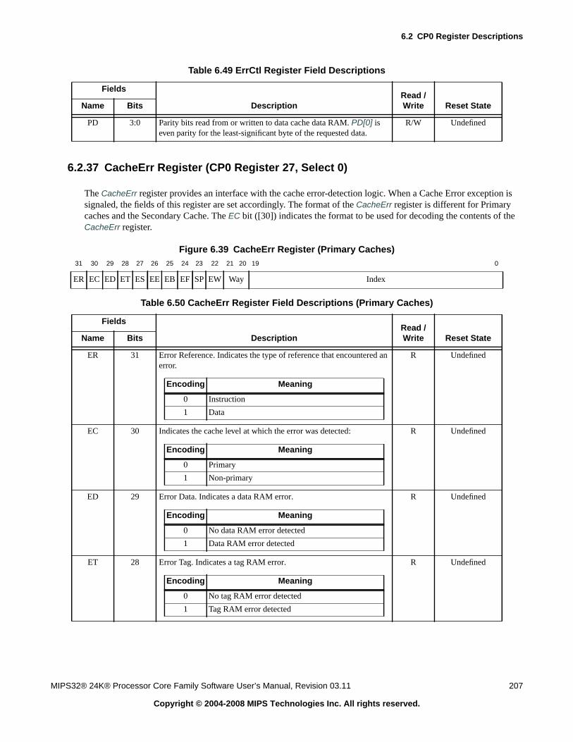
6.2 CP0 Register Descriptions
MIPS32® 24K® Processor Core Family Software User’s Manual, Revision 03.11 207
Copyright © 2004-2008 MIPS Technologies Inc. All rights reserved.
6.2.37 CacheErr Register (CP0 Register 27, Select 0)
The CacheErr register provides an interface with the cache error-detection logic. When a Cache Error exception issignaled, the fields of this register are set accordingly. The format of the CacheErr register is different for Primarycaches and the Secondary Cache. The EC bit ([30]) indicates the format to be used for decoding the contents of theCacheErr register.
Figure 6.39 CacheErr Register (Primary Caches)
PD 3:0 Parity bits read from or written to data cache data RAM. PD[0] iseven parity for the least-significant byte of the requested data.
R/W Undefined
31 30 29 28 27 26 25 24 23 22 21 20 19 0
ER EC ED ET ES EE EB EF SP EW Way Index
Table 6.50 CacheErr Register Field Descriptions (Primary Caches)
Fields
DescriptionRead /Write Reset StateName Bits
ER 31 Error Reference. Indicates the type of reference that encountered anerror.
R Undefined
EC 30 Indicates the cache level at which the error was detected: R Undefined
ED 29 Error Data. Indicates a data RAM error. R Undefined
ET 28 Error Tag. Indicates a tag RAM error. R Undefined
Table 6.49 ErrCtl Register Field Descriptions
Fields
DescriptionRead /Write Reset StateName Bits
Encoding Meaning
0 Instruction
1 Data
Encoding Meaning
0 Primary
1 Non-primary
Encoding Meaning
0 No data RAM error detected
1 Data RAM error detected
Encoding Meaning
0 No tag RAM error detected
1 Tag RAM error detected

CP0 Registers of the 24K® Core
208 MIPS32® 24K® Processor Core Family Software User’s Manual, Revision 03.11
Copyright © 2004-2008 MIPS Technologies Inc. All rights reserved.
ES 27 Error source. Indicates whether error was caused by internal proces-sor or external snoop request.
R Undefined
EE 26 Error external: Not supported. R 0
EB 25 Error Both. Indicates that a data cache error occurred in addition toan instruction cache error.
In the case of an additional data cache error, the remainder of thebits in this register are set according to the instruction cache error.
R Undefined
EF 24 Error Fatal. Indicates that a fatal cache error has occurred.There are a few situations where software will not be able to get allinformation about a cache error from the CacheErr register. Thesesituations are fatal because software cannot determine which mem-ory locations have been affected by the error. To enable software todetect these cases, the EF bit (bit 24) has been added to theCacheErr register.The following 6 cases are indicated as fatal cache errors by the EFbit:1 Dirty parity error in dirty victim (dirty bit cleared)2 Tag parity error in dirty victim3 Data parity error in dirty victim4 WB store miss and EW error at the requested index5 Dual/Triple errors from different transactions, e.g. scheduled
and non-scheduled load.6 Multiple data cache errors detected before the first instruction
of the cache error handler is issued.In addition to the above, simultaneous instruction and data cacheerrors as indicated by CacheErrEB will cause information about the
data cache error to be unavailable. However, that situation is notindicated by CacheErrEF.
R Undefined
SP 23 Scratchpad. Indicates Scratchpad RAM parity error. R 0
Table 6.50 CacheErr Register Field Descriptions (Primary Caches) (Continued)
Fields
DescriptionRead /Write Reset StateName Bits
Encoding Meaning
0 Error on internal request
1 Error on external request
Encoding Meaning
0 No additional data cache error
1 Additional data cache error
Encoding Meaning
0 No Scratchpad RAM error detected
1 Scratchpad RAM error detected

6.2 CP0 Register Descriptions
MIPS32® 24K® Processor Core Family Software User’s Manual, Revision 03.11 209
Copyright © 2004-2008 MIPS Technologies Inc. All rights reserved.
Figure 6.40 CacheErr Register (Secondary Cache)
EW 22 Error Way. Indicates a parity error on the dirty bits that are stored inthe way selection RAM array..
R Undefined
Way 21:20 Way. Specifies the cache way in which the error was detected. It isnot valid if a Tag RAM error is detected (ET=1) or Scratchpad RAMerror is detected (SP=1).
R Undefined
Index 19:0 Index. Specifies the cache or Scratchpad RAM index of the doubleword in which the error was detected. The way of the faulty cache iswritten by hardware in the Way field. Software must combine theWay and Index read in this register with cache configuration infor-mation in the Config1 register in order to obtain an index which canbe used in an indexed CACHE instruction to access the faulty cachedata or tag. Note that Index is aligned as a byte index, so it does notneed to be shifted by software before it is used in an indexedCACHE instruction. Index bits [4:3] are undefined upon tag RAMerrors, and Index bits above the MSB actually used for cache index-ing will also be undefined.Bits [19:16] are only used used for errors in the Scratchpad RAM.
R Undefined
31 30 29 28 27 26 25 24 23 22 21 19 18 0
EC ED ET EM EF EW Way Index
Table 6.51 CacheErr Register Field Descriptions (Secondary Cache)
Fields
DescriptionRead /Write Reset StateName Bits
Reserved 31 Reserved R Undefined
EC 30 Indicates the cache level at which the error was detected: R Undefined
ED 29 Error Data. Indicates a data RAM error. R Undefined
Table 6.50 CacheErr Register Field Descriptions (Primary Caches) (Continued)
Fields
DescriptionRead /Write Reset StateName Bits
Encoding Meaning
0 No way selection RAM error detected
1 Way selection RAM error detected
Encoding Meaning
0 Primary
1 Non-primary
Encoding Meaning
0 No data RAM error detected
1 Data RAM error detected

CP0 Registers of the 24K® Core
210 MIPS32® 24K® Processor Core Family Software User’s Manual, Revision 03.11
Copyright © 2004-2008 MIPS Technologies Inc. All rights reserved.
ET 28 Error Tag. Indicates a tag RAM error. R Undefined
Reserved 27 Reserved R Undefined
Reserved 26 Reserved R Undefined
EM 25 Error Multi. Indicates that a cache error occurred in multiple L2arrays.
In the case of multiple errors, the Tag ram error has the highest pri-ority, followed by the Data ram error, followed by the Way Selectram. Only the highest priority error information is recorded in theCacheErr register.
R Undefined
EF 24 Error Fatal. Indicates that a fatal cache error has occurred.There are a few situations where software will not be able to get allinformation about a cache error from the CacheErr register. Thesesituations are fatal because software cannot determine which mem-ory locations have been affected by the error. To enable software todetect these cases, the EF bit (bit 24) has been added to theCacheErr register.
This bit is set when a second L2 error occurs before taking theexception for the first L2 error.
R Undefined
Reserved 23 Reserved R Undefined
EW 22 Error Way. Indicates a way-selection RAM error. R Undefined
Way 21:19 Way. Specifies the cache way in which the error was detected. It isnot valid if a Tag RAM error is detected (ET=1) or Scratchpad RAMerror is detected (SP=1).
R Undefined
Table 6.51 CacheErr Register Field Descriptions (Secondary Cache) (Continued)
Fields
DescriptionRead /Write Reset StateName Bits
Encoding Meaning
0 No tag RAM error detected
1 Tag RAM error detected
Encoding Meaning
0 No multi error
1 Multi error
Encoding Meaning
0 No way-selection RAM error detected
1 Way-selection RAM error detected

6.2 CP0 Register Descriptions
MIPS32® 24K® Processor Core Family Software User’s Manual, Revision 03.11 211
Copyright © 2004-2008 MIPS Technologies Inc. All rights reserved.
6.2.38 ITagLo Register (CP0 Register 28, Select 0)
The ITagLo register acts as the interface to the instruction cache tag array. The Index Store Tag and Index Load Tagoperations of the CACHE instruction use the ITagLo register as the source of tag information. Note that the 24K coredoes not implement the ITagHi register.
When the WST bit of the ErrCtl register is asserted, this register becomes the interface to the way-selection RAM. Inthis mode, the fields are redefined to give appropriate access the contents of the WS array instead of the Tag array.Refer to Figure 8.2 for the layout of the way-selection RAM.
Figure 6.41 ITagLo Register Format (ErrCtlWST=0, ErrCtlSPR=0)
Figure 6.42 ITagLo Register Format (ErrCtlWST=1, ErrCtlSPR=0)
Figure 6.43 ITagLo Register Format (ErrCtlWST=0, ErrCtlSPR=1)
Index 18:0 Index. Specifies the cache index of the double word in which theerror was detected. The way of the faulty cache is written by hard-ware in the Way field. Software must combine the Way and Indexread in this register with cache configuration information in theConfig2 register in order to obtain an index which can be used in anindexed CACHE instruction to access the faulty cache data or tag.Note that Index is aligned as a byte index, so it does not need to beshifted by software before it is used in an indexed CACHE instruc-tion. Index bits [4:3] are undefined upon tag RAM errors and Indexbits above the MSB actually used for cache indexing will also beundefined.
R Undefined
31 11 10 9 8 7 6 5 4 1 0
PTagLo U R V R L R P
31 24 23 20 19 15 10 9 8 7 5 4 1 0
Unused WSLRU R Unused R U
tag 31 20 19 12 11 8 7 6 0
0 BasePA 0 E 0
1 0 Size 0
Table 6.52 ITagLo Register Field Descriptions
Fields
DescriptionRead /Write Reset StateName Bit(s)
Unused/U various Not used in certain modes of operation. R/W Undefined
Table 6.51 CacheErr Register Field Descriptions (Secondary Cache) (Continued)
Fields
DescriptionRead /Write Reset StateName Bits
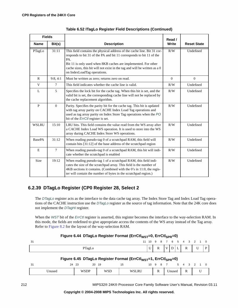
CP0 Registers of the 24K® Core
212 MIPS32® 24K® Processor Core Family Software User’s Manual, Revision 03.11
Copyright © 2004-2008 MIPS Technologies Inc. All rights reserved.
6.2.39 DTagLo Register (CP0 Register 28, Select 2
The DTagLo register acts as the interface to the data cache tag array. The Index Store Tag and Index Load Tag opera-tions of the CACHE instruction use the DTagLo register as the source of tag information. Note that the 24K core doesnot implement the DTagHi register.
When the WST bit of the ErrCtl register is asserted, this register becomes the interface to the way-selection RAM. Inthis mode, the fields are redefined to give appropriate access the contents of the WS array instead of the Tag array.Refer to Figure 8.2 for the layout of the way-selection RAM.
Figure 6.44 DTagLo Register Format (ErrCtlWST=0, ErrCtlSPR=0)
Figure 6.45 DTagLo Register Format (ErrCtlWST=1, ErrCtlSPR=0)
PTagLo 31:11 This field contains the physical address of the cache line. Bit 31 cor-responds to bit 31 of the PA and bit 11 corresponds to bit 11 of thePA.Bit 11 is only used when 8KB caches are implemented. For othercache sizes, this bit will not exist in the tag and will be written as a 0on IndexLoadTag operations.
R/W Undefined
R 9:8, 4:1 Must be written as zero; returns zero on read. 0 0
V 7 This field indicates whether the cache line is valid. R/W Undefined
L 5 Specifies the lock bit for the cache tag. When this bit is set, and thevalid bit is set, the corresponding cache line will not be replaced bythe cache replacement algorithm.
R/W Undefined
P 0 Parity. Specifies the parity bit for the cache tag. This bit is updatedwith tag array parity on CACHE Index Load Tag operations andused as tag array parity on Index Store Tag operations when the PObit of the ErrCtl register is set.
R/W Undefined
WSLRU 15:10 LRU bits. This field contains the value read from the WS array aftera CACHE Index Load WS operation. It is used to store into the WSarray during CACHE Index Store WS operations.
R/W Undefined
BasePA 31:12 When reading pseudo-tag 0 of a scratchpad RAM, this field willcontain bits [31:12] of the base address of the scratchpad region
R/W Undefined
E 7 When reading pseudo-tag 0 of a scratchpad RAM, this bit will indi-cate whether the scratchpad is enabled
R/W Undefined
Size 19:12 When reading pseudo-tag 1 of a scratchpad RAM, this field indi-cates the size of the scratchpad array. This field is the number of4KB sections it contains. (Combined with the 0’s in 11:0, the regis-ter will contain the number of bytes in the scratchpad region.)
R/W Undefined
31 11 10 9 8 7 6 5 4 3 2 1 0
PTagLo U R V D L R U P
31 24 23 20 19 15 10 9 8 7 5 4 3 2 1 0
Unused WSDP WSD WSLRU R Unused R U
Table 6.52 ITagLo Register Field Descriptions (Continued)
Fields
DescriptionRead /Write Reset StateName Bit(s)
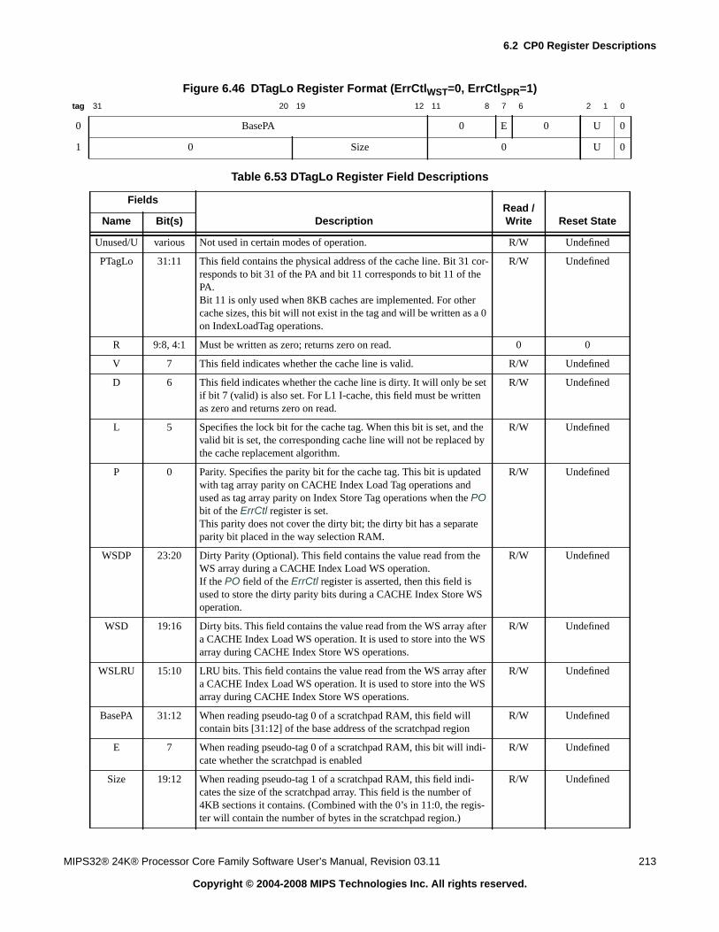
6.2 CP0 Register Descriptions
MIPS32® 24K® Processor Core Family Software User’s Manual, Revision 03.11 213
Copyright © 2004-2008 MIPS Technologies Inc. All rights reserved.
Figure 6.46 DTagLo Register Format (ErrCtlWST=0, ErrCtlSPR=1)tag 31 20 19 12 11 8 7 6 2 1 0
0 BasePA 0 E 0 U 0
1 0 Size 0 U 0
Table 6.53 DTagLo Register Field Descriptions
Fields
DescriptionRead /Write Reset StateName Bit(s)
Unused/U various Not used in certain modes of operation. R/W Undefined
PTagLo 31:11 This field contains the physical address of the cache line. Bit 31 cor-responds to bit 31 of the PA and bit 11 corresponds to bit 11 of thePA.Bit 11 is only used when 8KB caches are implemented. For othercache sizes, this bit will not exist in the tag and will be written as a 0on IndexLoadTag operations.
R/W Undefined
R 9:8, 4:1 Must be written as zero; returns zero on read. 0 0
V 7 This field indicates whether the cache line is valid. R/W Undefined
D 6 This field indicates whether the cache line is dirty. It will only be setif bit 7 (valid) is also set. For L1 I-cache, this field must be writtenas zero and returns zero on read.
R/W Undefined
L 5 Specifies the lock bit for the cache tag. When this bit is set, and thevalid bit is set, the corresponding cache line will not be replaced bythe cache replacement algorithm.
R/W Undefined
P 0 Parity. Specifies the parity bit for the cache tag. This bit is updatedwith tag array parity on CACHE Index Load Tag operations andused as tag array parity on Index Store Tag operations when the PObit of the ErrCtl register is set.This parity does not cover the dirty bit; the dirty bit has a separateparity bit placed in the way selection RAM.
R/W Undefined
WSDP 23:20 Dirty Parity (Optional). This field contains the value read from theWS array during a CACHE Index Load WS operation.If the PO field of the ErrCtl register is asserted, then this field isused to store the dirty parity bits during a CACHE Index Store WSoperation.
R/W Undefined
WSD 19:16 Dirty bits. This field contains the value read from the WS array aftera CACHE Index Load WS operation. It is used to store into the WSarray during CACHE Index Store WS operations.
R/W Undefined
WSLRU 15:10 LRU bits. This field contains the value read from the WS array aftera CACHE Index Load WS operation. It is used to store into the WSarray during CACHE Index Store WS operations.
R/W Undefined
BasePA 31:12 When reading pseudo-tag 0 of a scratchpad RAM, this field willcontain bits [31:12] of the base address of the scratchpad region
R/W Undefined
E 7 When reading pseudo-tag 0 of a scratchpad RAM, this bit will indi-cate whether the scratchpad is enabled
R/W Undefined
Size 19:12 When reading pseudo-tag 1 of a scratchpad RAM, this field indi-cates the size of the scratchpad array. This field is the number of4KB sections it contains. (Combined with the 0’s in 11:0, the regis-ter will contain the number of bytes in the scratchpad region.)
R/W Undefined

CP0 Registers of the 24K® Core
214 MIPS32® 24K® Processor Core Family Software User’s Manual, Revision 03.11
Copyright © 2004-2008 MIPS Technologies Inc. All rights reserved.
In addition to the three uses of the DTagLo register specified above, there is a fourth application where DTagLo isused to access the pseudo-tags (control registers) of the ITC block. This is done by executing the Index Store Tag orIndex Load Tag operation of the CACHE instruction with the ErrCtlITC set to 1 (and ErrCtlSPR/ErrCtlWST set to 0).
6.2.40 L23TagLo Register (CP0 Register 28, Select 4)
The L23TagLo register acts as the interface to the L2 or L3 cache tag array. The Index Store Tag and Index Load Tagoperations of the CACHE instruction use the L23TagLo register as the source of tag information. Note that the 24Kcore does not implement the L23TagHi register.
The definition of this register is dependent on the L2/L3 implementation. The core implements this as a general 32bR/W register.
6.2.41 IDataLo Register (CP0 Register 28, Select 1)
The IDataLo register is a register that acts as the interface to the instruction cache data array and is intended for diag-nostic operations only. The Index Load Tag operation of the CACHE instruction reads the corresponding data valuesinto the IDataLo register. If the WST bit in the ErrCtl register is set, then the contents of IDataLo can be written to thecache data array by doing an Index Store Data CACHE instruction. If the SPR bit in the ErrCtl register is set, then thecontents of IDataLo can be written to the scratchpad RAM data array by doing an Index Store Data CACHE instruc-tion.
Figure 6.47 IDataLo Register Format
6.2.42 DDataLo Register (CP0 Register 28, Select 3)
The DDataLo register is a register that acts as the interface to the data cache data array and is intended for diagnosticoperations only. The Index Load Tag operation of the CACHE instruction reads the corresponding data values intothe DDataLo register. If the WST bit in the ErrCtl register is set, then the contents of DDataLo can be written to thecache data array by doing an Index Store Data CACHE instruction. If the SPR bit in the ErrCtl register is set, then thecontents of DDataLo can be written to the scratchpad RAM data array by doing an Index Store Data CACHE instruc-tion.
Figure 6.48 DDataLo Register Format
31 0
DATA
Table 6.54 IDataLo Register Field Description
Fields
DescriptionRead /Write Reset StateName Bit(s)
DATA 31:0 Low-order data read from the cache data array. R/W Undefined
31 0
DATA

6.2 CP0 Register Descriptions
MIPS32® 24K® Processor Core Family Software User’s Manual, Revision 03.11 215
Copyright © 2004-2008 MIPS Technologies Inc. All rights reserved.
6.2.43 L23DataLo Register (CP0 Register 28, Select 5)
The L23DataLo register is a register that acts as the interface to the L2 or L3 cache data array and is intended for diag-nostic operations only. The Index Load Tag operation of the CACHE instruction reads the corresponding data valuesinto the L23DataLo register. If the WST bit in the ErrCtl register is set, then the contents of L23DataLo can be writtento the cache data array by doing an Index Store Data CACHE instruction. If the SPR bit in the ErrCtl register is set,then the contents of L23DataLo can be written to the scratchpad RAM data array by doing an Index Store DataCACHE instruction.
Figure 6.49 L23DataLo Register Format
6.2.44 IDataHi Register (CP0 Register 29, Select 1)
The IDataHi register is a register that acts as the interface to the cache data array and is intended for diagnostic opera-tions only. The Index Load Tag operation of the CACHE instruction reads the corresponding data values into theIDataHi register. If the WST bit in the ErrCtl register is set, then the contents of IDataHi can be written to the cachedata array by doing an Index Store Data CACHE instruction. If the SPR bit in the ErrCtl register is set, then the con-tents of IDataHi can be written to the scratchpad RAM data array by doing an Index Store Data CACHE instruction.
The interface to the I-cache only operates on pairs of instructions - the high instruction will be written into the IDataHiregister. Note that IDataHi and IDataLo reflect the memory ordering of the instructions. Depending on the endiannessof the system, Instruction0 belongs in either IDataHi (BigEndian) or IDataLo (LittleEndian) and vice versa forInstruction1.
Figure 6.50 IDataHi Register Format
Table 6.55 DDataLo Register Field Description
Fields
DescriptionRead /Write Reset StateName Bit(s)
DATA 31:0 Low-order data read from the cache data array. R/W Undefined
31 0
DATA
Table 6.56 L23DataLo Register Field Description
Fields
DescriptionRead /Write Reset StateName Bit(s)
DATA 31:0 Low-order data read from the cache data array. R/W Undefined
31 0
DATA
CP0 Registers of the 24K® Core
216 MIPS32® 24K® Processor Core Family Software User’s Manual, Revision 03.11
Copyright © 2004-2008 MIPS Technologies Inc. All rights reserved.
6.2.45 L23DataHi Register (CP0 Register 29, Select 5)
The L23DataHi register is a register that acts as the interface to the cache data array and is intended for diagnosticoperations only. The Index Load Tag operation of the CACHE instruction reads the corresponding data values intothe L23DataHi register. If the WST bit in the ErrCtl register is set, then the contents of L23DataHi can be written to thecache data array by doing an Index Store Data CACHE instruction.
Figure 6.51 L23DataHi Register Format
6.2.46 ErrorEPC (CP0 Register 30, Select 0)
The ErrorEPC register is a read/write register, similar to the EPC register, except that ErrorEPC is used on errorexceptions. All bits of the ErrorEPC register are significant and must be writable. It is also used to store the programcounter on Reset, Soft Reset, and nonmaskable interrupt (NMI) exceptions.
The ErrorEPC register contains the virtual address at which instruction processing can resume after servicing an error.This address can be:
• The virtual address of the instruction that caused the exception, or
• the virtual address of the immediately preceding branch or jump instruction when the error causing instruction isin a branch delay slot.
Unlike the EPC register, there is no corresponding branch delay slot indication for the ErrorEPC register.
In processors that implement the MIPS16 ASE, a read of the ErrorEPC register (via MFC0) returns the followingvalue in the destination GPR:
GPR[rt] ← ErrorExceptionPC31..1 || ISAMode0
That is, the upper 31 bits of the error exception PC are combined with the lower bit of the ISAMode field and writtento the GPR.
Table 6.57 IDataHi Register Field Description
Fields
DescriptionRead /Write Reset StateName Bit(s)
DATA 31:0 High-order data read from the cache data array. R/W Undefined
31 0
DATA
Table 6.58 L23DataHi Register Field Description
Fields
DescriptionRead /Write Reset StateName Bit(s)
DATA 31:0 High-order data read from the cache data array. R/W Undefined
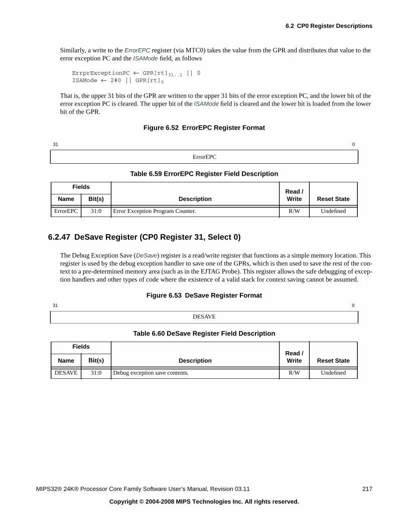
6.2 CP0 Register Descriptions
MIPS32® 24K® Processor Core Family Software User’s Manual, Revision 03.11 217
Copyright © 2004-2008 MIPS Technologies Inc. All rights reserved.
Similarly, a write to the ErrorEPC register (via MTC0) takes the value from the GPR and distributes that value to theerror exception PC and the ISAMode field, as follows
ErrprExceptionPC ← GPR[rt]31..1 || 0ISAMode ← 2#0 || GPR[rt]0
That is, the upper 31 bits of the GPR are written to the upper 31 bits of the error exception PC, and the lower bit of theerror exception PC is cleared. The upper bit of the ISAMode field is cleared and the lower bit is loaded from the lowerbit of the GPR.
Figure 6.52 ErrorEPC Register Format
6.2.47 DeSave Register (CP0 Register 31, Select 0)
The Debug Exception Save (DeSave) register is a read/write register that functions as a simple memory location. Thisregister is used by the debug exception handler to save one of the GPRs, which is then used to save the rest of the con-text to a pre-determined memory area (such as in the EJTAG Probe). This register allows the safe debugging of excep-tion handlers and other types of code where the existence of a valid stack for context saving cannot be assumed.
Figure 6.53 DeSave Register Format
31 0
ErrorEPC
Table 6.59 ErrorEPC Register Field Description
Fields
DescriptionRead /Write Reset StateName Bit(s)
ErrorEPC 31:0 Error Exception Program Counter. R/W Undefined
31 0
DESAVE
Table 6.60 DeSave Register Field Description
Fields
DescriptionRead /Write Reset StateName Bit(s)
DESAVE 31:0 Debug exception save contents. R/W Undefined

Chapter 7
MIPS32® 24K® Processor Core Family Software User’s Manual, Revision 03.11 218
Copyright © 2004-2008 MIPS Technologies Inc. All rights reserved.
Hardware and Software Initialization of the 24K® Core
A 24K processor core contains only a minimal amount of hardware initialization and relies on software to fully ini-tialize the device.
This chapter contains the following sections:
• Section 7.1 “Hardware-Initialized Processor State”
• Section 7.2 “Software Initialized Processor State”
7.1 Hardware-Initialized Processor State
A 24K processor core, like most other MIPS processors, is not fully initialized by hardware reset. Only a minimalsubset of the processor state is cleared. This is enough to bring the core up while running in unmapped and uncachedcode space. All other processor state can then be initialized by software. Unlike previous MIPS processors, there is nodistinction between cold and warm resets (or hard and soft resets). SI_Reset is used for both power-up reset and softreset.
7.1.1 Coprocessor 0 State
Much of the hardware initialization occurs in Coprocessor 0.
• Random - cleared to maximum value on Reset (TLB MMU only)
• Wired - cleared to 0 on Reset (TLB MMU only)
• StatusBEV - set to 1 on Reset
• StatusTS - cleared to 0 on Reset
• StatusNMI - cleared to 0 on Reset
• StatusERL - set to 1 on Reset
• StatusRP - cleared to 0 on Reset
• WatchLoI,R,W - cleared to 0 on Reset
• Config fields related to static inputs - set to input value by Reset
• ConfigK0 - set to 010 (uncached) on Reset
• ConfigKU - set to 010 (uncached) on Reset (FM MMU only)

7.2 Software Initialized Processor State
MIPS32® 24K® Processor Core Family Software User’s Manual, Revision 03.11 219
Copyright © 2004-2008 MIPS Technologies Inc. All rights reserved.
• ConfigK23 - set to 010 (uncached) on Reset (FM MMU only)
• DebugDM - cleared to 0 on Reset (unless EJTAGBOOT option is used to boot into DebugMode, see Chapter 11,“EJTAG Debug Support in the 24K® Core” on page 240 for details)
• DebugLSNM - cleared to 0 on Reset
• DebugIBusEP - cleared to 0 on Reset
• DebugDBusEP - cleared to 0 on Reset
• DebugIEXI - cleared to 0 on Reset
• DebugSSt - cleared to 0 on Reset
7.1.2 TLB Initialization
Each TLB entry has a “hidden” state bit, which is set by Reset and is cleared when the TLB entry is written. This bitdisables matches and prevents “TLB Shutdown” conditions from being generated by the power-up values in the TLBarray (when two or more TLB entries match on a single address). This bit is not visible to software.
7.1.3 Bus State Machines
When a Reset exception is taken, all pending bus transactions are aborted, and the state machines in the bus interfaceunit are reset.
7.1.4 Static Configuration Inputs
All static configuration inputs (for example, defining the bus mode and cache size) should only be changed duringReset.
7.1.5 Fetch Address
By default, the fetch is directed to VA 0xBFC00000 (PA 0x1FC00000) upon Reset. This address is in kseg1,which isunmapped and uncached, so that the TLB and caches do not require hardware initialization.
This initial fetch address can be overridden via core inputs. See Section 5.5 “Exception Vector Locations” for addi-tional details.
If EJTAGBOOT is active (see Section 11.3.3.8 “EJTAGBOOT Instruction” ), the processor will begin fetchinginstructions directly from the EJTAG probe rather than from memory.
7.2 Software Initialized Processor State
Software is required to initialize the following parts of the device.
Hardware and Software Initialization of the 24K® Core
220 MIPS32® 24K® Processor Core Family Software User’s Manual, Revision 03.11
Copyright © 2004-2008 MIPS Technologies Inc. All rights reserved.
7.2.1 Register File
The register file powers up in an unknown state with the exception of r0 which is always 0. Initializing the rest of theregister file is not required for proper operation. Good code will generally not read a register before writing to it, butthe boot code can initialize the register file for added safety.
7.2.2 TLB
Because of the hidden bit indicating initialization, the core does not initialize the TLB upon Reset. This is an imple-mentation specific feature of the 24K core and cannot be relied upon if writing generic code for MIPS32/64 proces-sors.
7.2.3 Caches
The cache tag and data arrays power up to an unknown state and are not affected by reset. Every tag in the cachearrays should be initialized to an invalid state using the CACHE instruction (typically the Index Invalidate function).This can be a long process, especially since the instruction cache initialization needs to be run in an uncached addressregion.
7.2.4 Coprocessor 0 State
Miscellaneous COP0 states need to be initialized prior to leaving the boot code. There are various exceptions whichare blocked by ERL=1 or EXL=1 and which are not cleared by Reset. These can be cleared to avoid taking spuriousexceptions when leaving the boot code.
• Cause: WP (Watch Pending), SW0/1 (Software Interrupts) should be cleared.
• Config: K0 (kseg0 Coherency Algorithm) should be set to the desired Cache Coherency Algorithm (CCA) priorto accessing kseg0.
• Config: (FM MMU only) KU and K23 should be set to the desired CCA for USeg/KUSeg and kseg2/3 respec-tively prior to accessing those regions.
• Count: Should be set to a known value if Timer Interrupts are used.
• Compare: Should be set to a known value if Timer Interrupts are used. The write to compare will also clear anypending Timer Interrupts (and thus, Count should be set before Compare, to avoid any unexpected interrupts).
• Status: Desired state of the device should be set.
• Other COP0 state: Other registers should be written before they are read. Some registers are not explicitly write-able, and are only updated as a by-product of instruction execution or a taken exception. Uninitialized bits shouldbe masked off after reading these registers.
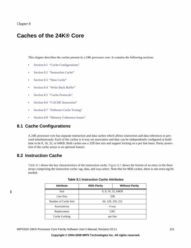
Chapter 8
MIPS32® 24K® Processor Core Family Software User’s Manual, Revision 03.11 221
Copyright © 2004-2008 MIPS Technologies Inc. All rights reserved.
Caches of the 24K® Core
This chapter describes the caches present in a 24K processor core. It contains the following sections:
• Section 8.1 “Cache Configurations”
• Section 8.2 “Instruction Cache”
• Section 8.3 “Data Cache”
• Section 8.4 “Write Back Buffer”
• Section 8.5 “Cache Protocols”
• Section 8.6 “CACHE Instruction”
• Section 8.7 “Software Cache Testing”
• Section 8.8 “Memory Coherence Issues”
8.1 Cache Configurations
A 24K processor core has separate instruction and data caches which allows instruction and data references to pro-ceed simultaneously. Each of the caches is 4-way set associative and they can be independently configured at buildtime to be 8, 16, 32, or 64KB. Both caches use a 32B line size and support locking on a per line basis. Parity protec-tion of the cache arrays is an optional feature.
8.2 Instruction Cache
Table 8.1 shows the key characteristics of the instruction cache. Figure 8.1 shows the format of an entry in the threearrays comprising the instruction cache: tag, data, and way-select. Note that for 8KB caches, there is one extra tag bitneeded.
Table 8.1 Instruction Cache Attributes
Attribute With Parity Without Parity
Size 0, 8, 16, 32, 64KB
Line Size 32B
Number of Cache Sets 64, 128, 256, 512
Associativity 4 way
Replacement LRU
Cache Locking per line

Caches of the 24K® Core
222 MIPS32® 24K® Processor Core Family Software User’s Manual, Revision 03.11
Copyright © 2004-2008 MIPS Technologies Inc. All rights reserved.
Figure 8.1 Instruction Cache Organization
8.2.1 Virtual Aliasing
The instruction cache on the 24K processor core is virtually indexed and physically tagged. The lower bits of the vir-tual address are used to access the cache arrays and the physical address is used in the tags. Because the way size canbe larger than the minimum TLB page size, there is a potential for virtual aliasing. This means that one physicaladdress can exist in multiple indices within the cache if it is accessed with different virtual addresses.
This reduces the cache efficiency somewhat, but is generally not a problem unless the instruction stream is beingwritten to. When instructions are written, software must ensure that the store data is written out to memory and theold data is invalidated in the instruction cache (via the CACHE or SYNCI instruction). For this to work correctly, theaddress must be invalidated from each of the possible alias locations. The 24K processor includes a feature to sim-plify this task and automatically invalidate the physical address from all of the alias locations. The presence of thisfeature and the enable for it are located in the Config7 register. Config7IAR =1 indicates that aliases are possible (cache> 16KB and TLB-based MMU) and this feature is present. This feature is enabled by default, but Config7IVA can beset to 1 to disable it. Looking up the other alias locations does slow down the invalidate slightly, so software can dis-able it when aliases are known not to be present, for example, when using an OS with 16KB TLB pages,
Data Array
Read Unit 79b x 4 70b x 4
Write Unit 79b 70b
Tag Array
Read Unit (8KB) 24b x 4 23b x 4
Read Unit (non-8KB) 23b x 4 22b x 4
Write Unit (8KB) 24b 23b
Write Unit (non-8KB) 23b 22b
Way-Select Array
Read Unit 6b
Write Unit 1-6b
Table 8.1 Instruction Cache Attributes
Attribute With Parity Without Parity
Tag (per way):
Data (per way)1:
Way-Select:
1 1 1 20/21
Parity Valid Lock PA[31:12/11]
9 6 64 9 6 64 9 6 64 9 6 64
Parity Precode dword3 Parity Precode dword2 Parity Precode dword1 Parity Precode dword0
6
LRU
1. Parity Bits in data array will be interleaved with precode and data bytes

8.3 Data Cache
MIPS32® 24K® Processor Core Family Software User’s Manual, Revision 03.11 223
Copyright © 2004-2008 MIPS Technologies Inc. All rights reserved.
8.2.2 Precode Bits
In order for the fetch unit to quickly detect branches and jumps when executing code, the instruction cache array con-tains some additional precode bits. These bits indicate the type and location of branch or jump instructions within a64b fetch bundle. These precode bits are not used when executing MIPS16e code.
8.2.3 Parity
Parity protection of the instruction cache arrays can optionally be included. The data array has a 9 parity bits - one forthe 6 precode bits and one for each byte of the 64b data. The tag array has a single parity bit for each tag. The LRUarray does not have any parity.
8.3 Data Cache
The data cache is similar to the instruction cache, with a few key differences:
• The data cache does not contain any precode information.
• To handle store bytes, the data array is byte accessible and the optional data parity is 1 bit per byte.
• The way-select array for the data cache also holds the dirty bits (and optional dirty parity bits) for each cacheline, in addition to the LRU information.
• Virtual aliases must be handled differently
Table 8.2 shows the key characteristics of the data cache. Figure 8.2 shows the format of an entry in the three arrayscomprising the data cache: tag, data, and way-select.
Table 8.2 Data Cache Attributes
Attribute With Parity Without Parity
Size 0, 8, 16, 32, 64KB
Line Size 32B
Number of Cache Sets 64, 128, 256, 512
Associativity 4 way
Replacement LRU
Cache Locking per line
Data Array
Read Unit 72b x 4 64b x 4
Write Unit 9b 8b
Tag Array
Read Unit (8KB) 24b x 4 23b x 4
Read Unit (non-8KB) 23b x 4 22b x 4
Write Unit (8KB) 24b 23b
Write Unit (non-8KB) 23b 22b
Way-Select Array

Caches of the 24K® Core
224 MIPS32® 24K® Processor Core Family Software User’s Manual, Revision 03.11
Copyright © 2004-2008 MIPS Technologies Inc. All rights reserved.
Figure 8.2 Data Cache Organization
8.3.1 Virtual Aliasing
Since the data cache is virtually indexed and physically tagged, a potential issue referred to as virtual aliasing mightexist. Virtual aliasing occurs if the virtual bits used to index a cache array are not consistent with the overlappingphysical bits, after the virtual address has been translated to a physical address. The possibility of virtual aliasing onlyoccurs in address regions which are mapped through a TLB-based memory management unit.
In TLB-mapped address regions, virtual aliasing may occur if the cache size per way is greater than the page size. Forexample, consider a 32KB cache organized as 4-way set associative. The size per way is then 8 KB, so virtual addressbits [12:0] are used to index the array. If the address is in a translated region with a page size of 4 KB, then addressbits [11:0] are untranslated but address bits [31:12] will be mapped and for these bits the virtual and physicaladdresses may be different. In this example, bit [12] could pose a potential problem due to virtual aliasing. Imaginetwo virtual addresses, VA0 and VA1, whose only difference is the value of bit [12], which map to the same physicaladdress. These two virtual addresses would be indexed to two different lines by the cache, even though they wereintended to represent the same physical address. Then if a program does a load using VA0 and a store using VA1, orvice-versa, the cache may not return the expected data.
Table 8.3 shows the overlapped virtual/physical address bits which could potentially be involved in virtual aliasing,given the possible minimum page sizes and cache way sizes supported by a 24K core. Virtual aliasing is generallyonly a problem for the D-cache, since stores don’t happen to the I-cache. A special hardware mechanism is availableto prevent the possibility of virtual aliasing in 32KB and 64KB data caches. In cores not configured with this mecha-nism, virtual aliasing must be handled by software. The software solution must ensure that the mapping of virtual
Read Unit 14b 10b
Write Unit 1-14b
Table 8.2 Data Cache Attributes (Continued)
Attribute With Parity Without Parity
Tag (per way):
Data (per way):
Way-Select:
1 1 1 20/21
Parity Valid Lock PA[31:12/11]
1 8 9x30 1 8
Parity Data31 ... Parity Data0
6 1 1 1 1 1 1 1 1
LRU Parity Dirty3 Parity Dirty2 Parity Dirty1 Parity Dirty0

8.4 Write Back Buffer
MIPS32® 24K® Processor Core Family Software User’s Manual, Revision 03.11 225
Copyright © 2004-2008 MIPS Technologies Inc. All rights reserved.
address bits which overlap with physical address bits be handled consistently. The simplest approach is to ensure thatthe overlapping bits are unity-mapped (VA equals PA).
A related issue can occur in virtually indexed, physically tagged caches if the number of physical bits stored in the tagarray does not fully overlap the physically translated bits for the smallest page size. For a 24K core, there are alwaysat least 20 address bits stored in the cache tag, representing bits [31:12] of the physical address. Since the minimumpage size is 4KB with bits [31:12] physically translated by the TLB, the cache tag size does overlap the translated bitsand this issue will not occur.
8.3.2 Parity
Parity protection of the data cache arrays can optionally be included. The data array requires a parity bit for each byte,to correspond to the minimum write quantum for a store. The tag array has a single parity bit for each tag. Theway-select array has separate parity bits to cover each dirty bit, but the LRU bits are not covered by parity.
8.4 Write Back Buffer
The BIU includes a Write Back Buffer (WBB) that holds writes going to memory. This includes evictions from thedata cache, as well as write-through stores, uncached stores, and uncached accelerated stores. The WBB consists of 4entries, each of which is capable of holding 32B of data. The WBB also holds L2 CACHE instructions that are to besent out on the bus.
The WBB will attempt to gather uncached accelerated (UCA)stores to allow full line burst writes. UCA behavior isdescribed in Section 8.4.1 “Uncached Accelerated Stores”. Write through stores can also be gathered in a WBB entryif ConfigMM= 1.
WBB entries are ‘flushed’ under a variety of conditions. When a buffer is flushed, the write command is queued inthe BIU and the WBB entry will not accept any more activity until the data has been written to the bus and the bufferis freed up. UCA flush conditions are described in the next section. Flush conditions for other types are shown here:
• Uncached (non-accelerated) stores flush immediately
• L2 CACHE instruction commands are also flushed immediately
• Entries for D$ evictions are flushed when all 4 dwords (32B) of data have been gathered
• Write-through entries are flushed under the following conditions:
• A full 32B line has been gathered
• A read request matches the address of the WT line. The write command will be ordered ahead of the readcommand. There is no direct bypass of the WBB data to the read—the read gets the data from memory.
Table 8.3 Potential Virtual Aliasing Bits
Minimum Page Size(KB) Cache Way Size (KB)
Overlapped addressbits with possible
aliasing
4 8 [12]
16 [13:12]
8 16 [13]

Caches of the 24K® Core
226 MIPS32® 24K® Processor Core Family Software User’s Manual, Revision 03.11
Copyright © 2004-2008 MIPS Technologies Inc. All rights reserved.
• A WT request to a different 32B line is seen. Only 1 WT merge can be active at any time.
8.4.1 Uncached Accelerated Stores
Uncached Accelerated gathering is supported for word and double word stores only.
Gathering of uncached accelerated stores will start on cache-line aligned addresses, i.e. 32 byte aligned addresses.Uncached accelerated word or double word stores that do not meet that condition will be treated like regularuncached stores.
An uncached accelerated store to the start of a new line will reserve a write-back buffer entry for gathering. Subse-quent uncached accelerated word or double word stores to the same cache line will write sequentially into this buffer,independent of the word address associated with these stores. The uncached accelerated buffer is tagged with theaddress of the first store.
An uncached accelerated buffer is written to memory (flushed) if:
1. The last word in the entry being gathered is written. (Implicit flush)
2. A PREF Nudge which match the address associated with the gather buffer (Explicit flush).
3. A SYNC instruction is executed. (Explicit flush)
4. Bits <31:5> of the address of a Load instruction match the address associated with the gather buffer. (Implicitflush)
5. Uncached Accelerated store to a different 32B line (Implicit flush)
6. An exception occurs. (Implicit flush)
When an uncached accelerated buffer is flushed, the address sent out on the system interface is the address associatedwith the gather buffer.
Caveats:
• Uncached Accelerated stores are not ordered with respect to uncached accesses. Any uncached stores and anyuncached loads to unrelated addresses that occur between uncached accelerated stores that are part of a gathersequence may occur out of order.
• The only constraint imposed on the gathering is that doubleword stores are only allowed to write to double wordaligned locations in the buffer. For example if uncached accelerated gathering starts with a Store Word (SW), itmay not immediately be followed by a Store Double (SDC1).
• Uncached accelerated stores of the following types are not intended to be used by software and may generateunpredictable results:
1. Sub-word (byte, halfword, tri-byte) Stores
2. Unaligned Stores
3. Store conditionals

8.5 Cache Protocols
MIPS32® 24K® Processor Core Family Software User’s Manual, Revision 03.11 227
Copyright © 2004-2008 MIPS Technologies Inc. All rights reserved.
• In order for software to be able to run functionally correct on implementations without uncached acceleratedstores, software should always generate accesses starting on a cache-line aligned address, proceed to generatecorrectly incremented sequential addresses and observe the restrictions for uncached accelerated stores.
8.5 Cache Protocols
This section describes cache organization, attributes, and cache-line replacement for the instruction and data caches.This section also discusses issues relating to virtual aliasing.
8.5.1 Cache Organization
The instruction and data caches each consist of three arrays: tag, data and way-select. The caches are virtuallyindexed, since a virtual address is used to select the appropriate line within each of the three arrays. The caches arephysically tagged, as the tag array contains a physical, not virtual, address.
The tag and data arrays hold 4 ways of information per set, corresponding to the 4-way set associativity of the cache.The way-select array holds information to choose the way to be filled, as well as dirty bits in the case of the datacache.
Figure 8.1 (instruction cache) and Figure 8.2 (data cache) show the format of each line in the tag, data and way-selectarrays.
A tag entry consists of the upper 20 or 21 bits of the physical address (bits [31:12/11]) (bit 11 is only used for 8KBcaches), one valid bit for the line, and a lock bit. A data entry contains the four 64-bit doublewords in the line, for atotal of 32 bytes. All four words in the line are present or not in the data array together, hence the single valid bitstored with the tag. Once a valid line is resident in the cache, byte, halfword, triple-byte or full word stores can updateall or a portion of the words in that line. The tag and data entries are repeated for each of the 4 lines in the set.
A way-select entry holds bits choosing the way to be replaced according to a Least Recently Used (LRU) algorithm.The LRU information applies to all the ways and there is one way-select entry for all the ways in the set. The arraywith way-select entries for the data cache also holds dirty bits for the lines. One dirty bit is required per line, as shownin Figure 8.2. The instruction cache only supports reads, hence only LRU entries are stored in the instructionway-select array.
8.5.2 Cacheability Attributes
A 24K core supports the following cacheability attributes:
• Uncached: Addresses in a memory area indicated as uncached are not read from the cache. Stores to suchaddresses are written directly to main memory, without changing cache contents.
• Write-back with write allocation: Loads and instruction fetches first search the cache, reading main memory onlyif the desired data does not reside in the cache. On data store operations, the cache is first searched to see if thetarget address is cache resident. If it is resident, the cache contents are updated, but main memory is not written.If the cache lookup misses on a store, main memory is read to bring the line into the cache and merge it with thenew store data. Hence, the allocation policy on a cache miss is read- or write-allocate. Data stores will update theappropriate dirty bit in the way-select array to indicate that the line contains modified data. When a line withdirty data is displaced from the cache, it is written back to memory.
• Write-through with no write allocation: Loads and instruction fetches first search the cache, reading main mem-ory only if the desired data does not reside in the cache. On data store operations, the cache is first searched to

Caches of the 24K® Core
228 MIPS32® 24K® Processor Core Family Software User’s Manual, Revision 03.11
Copyright © 2004-2008 MIPS Technologies Inc. All rights reserved.
see if the target address is cache resident. If it is resident, the cache contents are updated, and main memory isalso written. If the cache lookup misses on a store, only main memory is written. Hence, the allocation policy ona cache miss is read-allocate only.NOTE: The instruction cache always uses a writeback CCA for its bus requests even when the TLB page ismapped as write-through.
• Uncached Accelerated: Uncached stores are gathered together for more efficient bus utilization. See Section8.4.1 “Uncached Accelerated Stores” for more details
Some segments of memory employ a fixed caching policy; for example kseg1 is always uncacheable. Other segmentsof memory allow the caching policy to be selected by software. Generally, the cache policy for these programmableregions is defined by a cacheability attribute field associated with that region of memory. See Chapter 4, “MemoryManagement of the 24K® Core” on page 87 for further details.
8.5.3 Replacement Policy
The replacement policy refers to how a way is chosen to hold an incoming cache line on a miss which will result in acache fill. The replacement policy is least recently used (LRU), but excluding any locked ways. The LRU bit(s) in theway-select array encode the order in which ways on that line have been accessed.
On a cache miss, the lock and LRU bits for the tag and way-select entries of the selected line may be used to deter-mine the way which will be chosen.
The LRU field in the way select array is updated as follows:
• On a cache hit, the associated way is updated to be the most recently used. The order of the other ways relative toeach another is unchanged.
• On a cache refill, the filled way is updated to be the most recently used.
• On CACHE instructions, the update of the LRU bits depends on the type of operation to be performed:
• Index (Writeback) Invalidate: Least-recently used.
• Index Load Tag: No update.
• Index Store Tag, WST=0: Most-recently used if valid bit is set in TagLo CP0 register. Least-recently usedif valid bit is cleared in TagLo CP0 register.
• Index Store Tag, WST=1: Update the field with the contents of the TagLo CP0 register (refer to Table 8.4for the valid values of this field).
• Index Store Data: No update.
• Hit Invalidate: Least-recently used if a hit is generated, otherwise unchanged.
• Fill: Most-recently used.
• Hit (Writeback) Invalidate: Least-recently used if a hit is generated, otherwise unchanged.
• Hit Writeback: No update.
• Fetch and Lock: For instruction cache, no update. For data cache, most-recently used.

8.6 CACHE Instruction
MIPS32® 24K® Processor Core Family Software User’s Manual, Revision 03.11 229
Copyright © 2004-2008 MIPS Technologies Inc. All rights reserved.
If all ways are valid, then any locked ways will be excluded from consideration for replacement. For the unlockedways, the LRU bits are used to identify the way which has been used least recently, and that way is selected forreplacement.
If the way selected for replacement has its dirty bit asserted in the way-select array, then that 32-byte line will be writ-ten back to memory before the new fill can occur.
8.5.4 Line Locking
• The 24K core supports line locking in both caches. A line can be locked by either Fetch and Lock or Index StoreTag CACHE instructions.The core does not support the locking of all 4 ways of either cache at a particular index.If all 4 ways of the cache at a given index are locked, subsequent cache misses at that cache index will displaceone of the locked lines.
8.6 CACHE Instruction
Both caches support the CACHE instructions, which allow users to manipulate the contents of the Data and Tagarrays, including the locking of individual cache lines. These instructions are described in detail in Chapter 12,“24K® Processor Core Instructions” on page 303.
The CACHE Index Load Tag and Index Store Tag instructions can be used to read and write the WS- RAM by settingthe WST bit in the ErrCtl register. (The ErrCtl register is described in Section 6.2.36 “ErrCtl Register (CP0 Register26, Select 0)”.) Similarly, the SPR bit in the ErrCtl register will cause Index Load Tag and Index Store Tag instruc-tions to access the pseudo-tags associated with the scratchpad RAM array. Note that when the WST and SPR bits arezero, the CACHE index instructions access the cache Tag array.
Not all values of the WS field are valid for defining the order in which the ways are selected. This is only an issue,however, if the WS-RAM is written after the initialization (invalidation) of the Tag array. Valid WS field encodingsfor way selection order is shown in Table 8.4.
Table 8.4 Way Selection Encoding, 4 Ways
Selection Order1
1. The order is indicated by listing the least-recently used way to the left and themost-recently used way to the right, etc.
WS[5:0] Selection Order WS[5:0]
0123 000000 2013 100010
0132 000001 2031 110010
0213 000010 2103 100110
0231 010010 2130 101110
0312 010001 2301 111010
0321 010011 2310 111110
1023 000100 3012 011001
1032 000101 3021 011011
1203 100100 3102 011101
1230 101100 3120 111101
1302 001101 3201 111011
1320 101101 3210 111111

Caches of the 24K® Core
230 MIPS32® 24K® Processor Core Family Software User’s Manual, Revision 03.11
Copyright © 2004-2008 MIPS Technologies Inc. All rights reserved.
8.7 Software Cache Testing
Typically, the cache RAM arrays will be tested using BIST. It is, however, possible for software running on the pro-cessor to test all of the arrays. Of course, testing of the I-cache arrays should be done from an uncacheable space withinterrupts disabled in order to maintain the cache contents. There are multiple methods for testing these arrays in soft-ware, only one is presented here.
8.7.1 I-Cache and D-cache Tag Arrays
These arrays can be tested via the Index Load Tag and Index Store Tag varieties of the CACHE instruction. IndexStore Tag will write the contents of the TagLo register into the selected tag entry. Index Load Tag will read theselected tag entry into the TagLo.
If parity is implemented, the parity bits can be tested as a normal bit by setting the PO bit in the ErrCtl register. Thiswill override the parity calculation and write P bit in TagLo as the parity value.
8.7.2 I-Cache Data Array
This array can be tested using the Index Store Data and Index Load Tag varieties of the CACHE instruction. TheIndex Store Data variety is enabled by setting the WST bit in the ErrCtl register.
The precode bits in the array can be tested by setting the PCO bit in the ErrCtl register. This will write the PCI field inthe ErrCtl register instead of calculating the precode bits on a write.
The parity bits in the array can be tested by setting the PO bit in the ErrCtl register. This will use the PI field in ErrCtlinstead of calculating the parity on a write.
The rest of the data bits are read/written to/from the DataLo and DataHi registers.
8.7.3 I-Cache WS Array
The testing of this array is done with via Index Load Tag and Index Store Tag CACHE instructions. By setting theWST bit in the ErrCtl register, these operations will read and write the WS array instead of the tag array.
8.7.4 D-Cache Data Array
This array can be tested using the Index Store Tag CACHE, SW, and LW instructions. First, use Index Store Tag toset the initial state of the tags to valid with a known physical address (PA). Write the array using SW instructions tothe PAs that are resident in the cache. The value can then be read using LW instructions and compared to theexpected data.
The parity bits can be implicitly tested using this mechanism. The parity bits can be explicitly tested by setting the PObit in ErrCtl and using Index Store Data and Index Load Tag CACHE operations. The parity bits (one bit per byte) areread/written to/from the PD field in ErrCtl. Unlike the I-cache, the DataHi register is not used and only 32b of data isread/written per operation.
8.7.5 D-cache WS Array
The dirty bits in this array will be tested when the data tag is tested. The LRU bits can be tested using the same mech-anism as the I-cache WS array.

8.8 Memory Coherence Issues
MIPS32® 24K® Processor Core Family Software User’s Manual, Revision 03.11 231
Copyright © 2004-2008 MIPS Technologies Inc. All rights reserved.
8.8 Memory Coherence Issues
A cache presents coherency issues within the memory hierarchy which must be considered in the system design.Since a cache holds a copy of memory data, it is possible for another memory master to modify a memory location,thus making other copies of that location stale if those copies are still in use. A detailed discussion of memory coher-ence is beyond the scope of this document, but following are a few related comments.
A24K processor contains no direct hardware support for managing coherency with respect to its caches, so it must behandled via system design or software. The data cache supports either write-back or write-through protocols.
In write-through mode, all data writes will eventually be sent to memory. Due to write buffers, however, there couldbe a delay in how long it takes for the write to memory to actually occur. If another memory master updates cacheablememory which could also be in the cores caches, then those locations may need to be flushed from the cache. Theonly way to accomplish this invalidation is by use of the CACHE instruction.
In write-back mode, data writes only go to the cache and not to memory. So the processor cache may contain the onlycopy of data in the system until that data is written to main memory. Dirty lines are only written to memory when dis-placed from the cache as a new line is filled or if explicitly forced by certain flavors of the CACHE or PREF instruc-tions.
The SYNC instruction may also be useful to software enforcing memory coherence, as it flushes the core’s write buff-ers.

Chapter 9
MIPS32® 24K® Processor Core Family Software User’s Manual, Revision 03.11 232
Copyright © 2004-2008 MIPS Technologies Inc. All rights reserved.
Power Management in the 24K® Core
A 24K processor core offers a number of power management features, including low-power design, active powermanagement and power-down modes of operation. The core is a static design that supports changing the clock fre-quency or even stopping the clocks to manage power. The WAIT instruction suspends execution until an interrupt isdetected and can put the core into a low power mode.
The core provides two basic mechanisms for system level low-power support discussed in the following sections.
• Section 9.1 “Register-Controlled Power Management”
• Section 9.2 “Instruction-Controlled Power Management”
9.1 Register-Controlled Power Management
The RP bit in the CP0 Status register enables a standard software mechanism for placing the system into a low powerstate. The state of the RP bit is available externally via the SI_RP output signal. Three additional pins, SI_EXL,SI_ERL, and EJ_DebugM support the power management function by allowing the user to change the power state ifan exception or error occurs while the core is in a low power state.
Setting the RP bit of the CP0 Status register causes the core to assert the SI_RP signal. The external agent can thendecide whether to reduce the clock frequency and place the core into power down mode.
If an interrupt is taken while the device is in power down mode, that interrupt may need to be serviced depending onthe needs of the application. The interrupt causes an exception which in turn causes the EXL bit to be set. The settingof the EXL bit causes the assertion of the SI_EXL signal on the external bus, indicating to the external agent that aninterrupt has occurred. At this time the external agent can choose to either speed up the clocks and service the inter-rupt or let it be serviced at the lower clock speed.
The setting of the ERL bit causes the assertion of the SI_ERL signal on the external bus, indicating to the externalagent that an error has occurred. At this time the external agent can choose to either speed up the clocks and servicethe error or let it be serviced at the lower clock speed.
Similarly, the EJ_DebugM signal indicates that the processor is in debug mode. Debug mode is entered when the pro-cessor takes a debug exception. If fast handling of this is desired, the external agent can speed up the clocks.
The core provides four power down signals that are part of the system interface. Three of the pins change state as thecorresponding bits in the CP0 Status register are set or cleared. The fourth pin indicates that the processor is in debugmode:
• The SI_RP signal represents the state of the RP bit (27) in the CP0 Status register.
• The SI_EXL signal represents the state of the EXL bit (1) in the CP0 Status register.
• The SI_ERL signal represents the state of the ERL bit (2) in the CP0 Status register.

9.2 Instruction-Controlled Power Management
MIPS32® 24K® Processor Core Family Software User’s Manual, Revision 03.11 233
Copyright © 2004-2008 MIPS Technologies Inc. All rights reserved.
• The EJ_DebugM signal indicates that the processor has entered debug mode.
9.2 Instruction-Controlled Power Management
A second mechanism for invoking power down mode is through execution of the WAIT instruction. The WAITinstruction brings the processor into a low power state where the internal clocks are suspended and the pipeline is fro-zen. However, the internal timer and some of the input pins (SI_Int[5:0], SI_NMI, SI_Reset, and EJ_DINT) continue torun. The clocks are not shut down until all bus and coprocessor transactions have completed. Once the CPU is ininstruction controlled power management mode, any enabled interrupt, NMI, debug interrupt, or reset conditioncauses the CPU to exit this mode and resume normal operation. While the is in this low-power mode, the SI_SLEEPsignal is asserted to indicate to external agents what the state of the chip is.
9.2.1 Wait IE Ignore
A feature is included in the core that simplifies the task of using the WAIT instruction in the idle loop of an OS. TheWAIT instruction is typically in block of code where the OS first checks to see if there is any pending work and ifthere is not, it will execute the WAIT as shown below.
if (!pending){
wait();}
There is a tricky race condition present in this code. If an interrupt arrives between the pending check and the WAITinstruction, the service routine will return and execute the WAIT and go to sleep. However, the interrupt may havebeen enabling some pending work to be done in the ‘bottom-half’ processing. If the core goes back to sleep, thispending work will not be done until the next interrupt arrives.
The OS can check to see if the interrupt was signalled in this window and adjust the EPC value to before the pendingcheck, but this involves a fair amount of work. The Wait IE Ignore feature enables a simpler solution for the race con-dition. With this feature, a WAIT condition will be terminated by an active interrupt signal, even if that signal is pre-vented from causing an interrupt by StatusIE being clear or TCStatusIXMT being set. This allows interrupts to bedisabled in this section of code while still allowing the WAIT to complete.
An example of the assembly code for making use of this feature follows:
LEAF(r4k_wait).set push.set noreorderdi t4 # Clear Status.IE and preserve old value in t4LONG_L t0, ti_flags($28) # Get flag bitsandi t0, _TIF_NEED_RESCHED # Isolate reschedule flagbnez t0, 1f # branch around wait if pending worknopwait1: mtc0t4, C0_Status # restore status register.set popjr ranopEND(r4k_wait)

Power Management in the 24K® Core
234 MIPS32® 24K® Processor Core Family Software User’s Manual, Revision 03.11
Copyright © 2004-2008 MIPS Technologies Inc. All rights reserved.
Note that this sequence would not be safe to execute on a core without this feature. In that case, a normal interruptwill generally not wake up the core if StatusIE=0. The Config7WII bit indicates whether this feature is present on thecore.

Chapter 10
MIPS32® 24K® Processor Core Family Software User’s Manual, Revision 03.11 235
Copyright © 2004-2008 MIPS Technologies Inc. All rights reserved.
Instruction Set Overview
This chapter provides a general overview on the three CPU instruction set formats of the MIPS architecture: Immedi-ate, Jump, and Register. Refer to Chapter 12, “24K® Processor Core Instructions” on page 303 for a complete listingand description of instructions.
This chapter discusses the following topics
• Section 10.1 “CPU Instruction Formats”
• Section 10.2 “Load and Store Instructions”
• Section 10.3 “Computational Instructions”
• Section 10.4 “Jump and Branch Instructions”
• Section 10.5 “Control Instructions”
• Section 10.6 “Coprocessor Instructions”
10.1 CPU Instruction Formats
Each CPU instruction consists of a single 32-bit word, aligned on a word boundary. There are three instruction for-mats immediate (I-type), jump (J-type), and register (R-type)—as shown in Figure 10.1. The use of a small number ofinstruction formats simplifies instruction decoding, allowing the compiler to synthesize more complicated (and lessfrequently used) operations and addressing modes from these three formats as needed.

Instruction Set Overview
236 MIPS32® 24K® Processor Core Family Software User’s Manual, Revision 03.11
Copyright © 2004-2008 MIPS Technologies Inc. All rights reserved.
Figure 10.1 Instruction Formats
10.2 Load and Store Instructions
Load and store instructions are immediate (I-type) instructions that move data between memory and the general reg-isters. The only addressing mode that integer load and store instructions directly support is base register plus 16-bitsigned immediate offset. Floating point load and store instructions can use either that addressing mode or register plusregister indexed addressing.
10.2.1 Scheduling a Load Delay Slot
A load instruction that does not allow its result to be used by the instruction immediately following is called a delayedload instruction. The instruction slot immediately following this delayed load instruction is referred to as the loaddelay slot.
In a 24K core, the instruction immediately following a load instruction can use the contents of the loaded register;however in such cases hardware interlocks insert additional real cycles. Although not required, the scheduling of loaddelay slots can be desirable, both for performance and R-Series processor compatibility.
10.2.2 Defining Access Types
Access type indicates the size of a core data item to be loaded or stored, set by the load or store instruction opcode.
op 6-bit operation code
rs 5-bit source register specifier
rt 5-bit target (source/destination) register or branchcondition
immediate 16-bit immediate value, branch displacement oraddress displacement
target 26-bit jump target address
rd 5-bit destination register specifier
sa 5-bit shift amount
funct 6-bit function field
I-Type (Immediate)
R-Type (Register)
J-Type (Jump)
immediate
015
rt
1620
op
2631
rs
2125
target
015
op
2631
rt
1620
op
2631
rs
2125
sa
610
rd
1115
funct
05
target
025
op
2631

10.3 Computational Instructions
MIPS32® 24K® Processor Core Family Software User’s Manual, Revision 03.11 237
Copyright © 2004-2008 MIPS Technologies Inc. All rights reserved.
Regardless of access type or byte ordering (endianness), the address given specifies the low-order byte in theaddressed field. For a big-endian configuration, the low-order byte is the most-significant byte; for a little-endianconfiguration, the low-order byte is the least-significant byte.
The access type, together with the three low-order bits of the address, define the bytes accessed within the addressedword as shown in Table 10.1. Only the combinations shown in Table 10.1 are permissible; other combinations causeaddress error exceptions.
Instruction fetches are either halfword accesses (MIPS16e™ code) or word accesses (32b code). These referenceswill be impacted by endianness the same as load/store references of those sizes.
10.3 Computational Instructions
Computational instructions can be either in register (R-type) format, in which both operands are registers, or in imme-diate (I-type) format, in which one operand is a 16-bit immediate.
Computational instructions perform the following operations on register values:
• Arithmetic
Table 10.1 Byte Access Within a Doubleword
Access Type
Low-OrderAddress Bits
Bytes Accessed
Big Endian(63----------------31-------------------0)
Little Endian(63----------------31-------------------0)
2 1 0 Byte Byte
Doubleword 0 0 0 0 1 2 3 4 5 6 7 7 6 5 4 3 2 1 0
Word 0 0 0 0 1 2 3 3 2 1 0
1 0 0 4 5 6 7 7 6 5 4
Triplebyte 0 0 0 0 1 2 2 1 0
0 0 1 1 2 3 3 2 1
1 0 0 4 5 6 6 5 4
1 0 1 5 6 7 7 6 5
Halfword 0 0 0 0 1 1 0
0 1 0 2 3 3 2
1 0 0 4 5 5 4
1 1 0 6 7 7 6
Byte 0 0 0 0 0
0 0 1 1 1
0 1 0 2 2
0 1 1 3 3
1 0 0 4 4
1 0 1 5 5
1 1 0 6 6
1 1 1 7 7

Instruction Set Overview
238 MIPS32® 24K® Processor Core Family Software User’s Manual, Revision 03.11
Copyright © 2004-2008 MIPS Technologies Inc. All rights reserved.
• Logical
• Shift
• Count Leading Zeros/Ones
• Multiply
• Divide
These operations fit in the following four categories of computational instructions:
• ALU Immediate instructions
• Three-operand Register-type Instructions
• Shift Instructions
• Multiply And Divide Instructions
10.3.1 Cycle Timing for Multiply and Divide Instructions
Any multiply instruction in the integer pipeline is transferred to the multiplier as remaining instructions continuethrough the pipeline; the product of the multiply instruction is saved in the HI and LO registers. If the multiplyinstruction is followed by an MFHI or MFLO before the product is available, the pipeline interlocks until this productdoes become available. Refer to Chapter 2, “Pipeline of the 24K® Core” on page 31 for more information on instruc-tion latency and repeat rates.
10.4 Jump and Branch Instructions
Jump and branch instructions change the control flow of a program. All jump and branch instructions occur with adelay of one instruction: that is, the instruction immediately following the jump or branch (this is known as theinstruction in the delay slot) always executes while the target instruction is being fetched from storage.
10.4.1 Overview of Jump Instructions
Subroutine calls in high-level languages are usually implemented with Jump or Jump and Link instructions, both ofwhich are J-type instructions. In J-type format, the 26-bit target address shifts left 2 bits and combines with thehigh-order 4 bits of the current program counter to form an absolute address.
Returns, dispatches, and large cross-page jumps are usually implemented with the Jump Register or Jump and LinkRegister instructions. Both are R-type instructions that take the 32-bit byte address contained in one of the generalpurpose registers.
For more information about jump instructions, refer to the individual instructions in MIPS32® Architecture Refer-ence Manual, Volume II: The MIPS32® Instruction Set.
10.4.2 Overview of Branch Instructions
All branch instruction target addresses are computed by adding the address of the instruction in the delay slot to the16-bit offset (shifted left 2 bits and sign-extended to 32 bits). All branches occur with a delay of one instruction.

10.5 Control Instructions
MIPS32® 24K® Processor Core Family Software User’s Manual, Revision 03.11 239
Copyright © 2004-2008 MIPS Technologies Inc. All rights reserved.
If a conditional branch likely is not taken, the instruction in the delay slot is nullified.
Branches, jumps, ERET, and DERET instructions should not be placed in the delay slot of a branch or jump.
10.5 Control Instructions
Control instructions allow the software to initiate traps; they are always R-type.
10.6 Coprocessor Instructions
CP0 instructions perform operations on the System Control Coprocessor registers to manipulate the memory manage-ment and exception handling facilities of the processor. Refer to Chapter 12, “24K® Processor Core Instructions” onpage 303 for a listing of CP0 instructions.

Chapter 11
MIPS32® 24K® Processor Core Family Software User’s Manual, Revision 03.11 240
Copyright © 2004-2008 MIPS Technologies Inc. All rights reserved.
EJTAG Debug Support in the 24K® Core
The EJTAG debug logic in the 24K processor core is compliant with EJTAG Specification 3.20 and includes:
1. Standard core debug features
2. Optional hardware breakpoints
3. Standard Test Access Port (TAP) for a dedicated connection to a debug host
4. Optional MIPS Trace capability for program counter/data address/data value trace to On-chip memory or toTrace probe
This chapter contains the following sections:
• Section 11.1 “Debug Control Register”
• Section 11.2 “Hardware Breakpoints”
• Section 11.3 “Test Access Port (TAP)”
• Section 11.4 “EJTAG TAP Registers”
• Section 11.5 “TAP Processor Accesses”
• Section 11.6 “PC Sampling”
• Section 11.7 “MIPS® Trace”
• Section 11.8 “PDtrace™ Registers (Software Control)”
• Section 11.9 “Trace Control Block (TCB) Registers (Hardware Control)”
• Section 11.10 “Enabling MIPS Trace”
• Section 11.11 “TCB Trigger Logic”
• Section 11.12 “MIPS Trace Cycle-by-Cycle Behavior”
• Section 11.13 “TCB On-Chip Trace Memory”
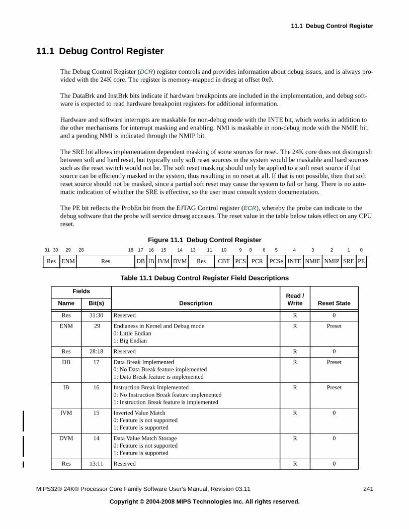
11.1 Debug Control Register
MIPS32® 24K® Processor Core Family Software User’s Manual, Revision 03.11 241
Copyright © 2004-2008 MIPS Technologies Inc. All rights reserved.
11.1 Debug Control Register
The Debug Control Register (DCR) register controls and provides information about debug issues, and is always pro-vided with the 24K core. The register is memory-mapped in drseg at offset 0x0.
The DataBrk and InstBrk bits indicate if hardware breakpoints are included in the implementation, and debug soft-ware is expected to read hardware breakpoint registers for additional information.
Hardware and software interrupts are maskable for non-debug mode with the INTE bit, which works in addition tothe other mechanisms for interrupt masking and enabling. NMI is maskable in non-debug mode with the NMIE bit,and a pending NMI is indicated through the NMIP bit.
The SRE bit allows implementation dependent masking of some sources for reset. The 24K core does not distinguishbetween soft and hard reset, but typically only soft reset sources in the system would be maskable and hard sourcessuch as the reset switch would not be. The soft reset masking should only be applied to a soft reset source if thatsource can be efficiently masked in the system, thus resulting in no reset at all. If that is not possible, then that softreset source should not be masked, since a partial soft reset may cause the system to fail or hang. There is no auto-matic indication of whether the SRE is effective, so the user must consult system documentation.
The PE bit reflects the ProbEn bit from the EJTAG Control register (ECR), whereby the probe can indicate to thedebug software that the probe will service dmseg accesses. The reset value in the table below takes effect on any CPUreset.
Figure 11.1 Debug Control Register31 30 29 28 18 17 16 15 14 13 11 10 9 8 6 5 4 3 2 1 0
Res ENM Res DB IB IVM DVM Res CBT PCS PCR PCSe INTE NMIE NMIP SRE PE
Table 11.1 Debug Control Register Field Descriptions
Fields
DescriptionRead /Write Reset StateName Bit(s)
Res 31:30 Reserved R 0
ENM 29 Endianess in Kernel and Debug mode0: Little Endian1: Big Endian
R Preset
Res 28:18 Reserved R 0
DB 17 Data Break Implemented0: No Data Break feature implemented1: Data Break feature is implemented
R Preset
IB 16 Instruction Break Implemented0: No Instruction Break feature implemented1: Instruction Break feature is implemented
R Preset
IVM 15 Inverted Value Match0: Feature is not supported1: Feature is supported
R 0
DVM 14 Data Value Match Storage0: Feature is not supported1: Feature is supported
R 0
Res 13:11 Reserved R 0
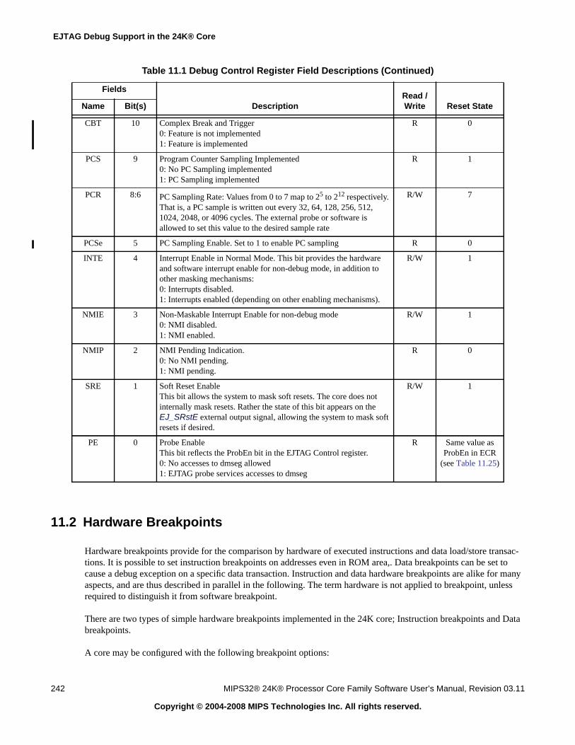
EJTAG Debug Support in the 24K® Core
242 MIPS32® 24K® Processor Core Family Software User’s Manual, Revision 03.11
Copyright © 2004-2008 MIPS Technologies Inc. All rights reserved.
11.2 Hardware Breakpoints
Hardware breakpoints provide for the comparison by hardware of executed instructions and data load/store transac-tions. It is possible to set instruction breakpoints on addresses even in ROM area,. Data breakpoints can be set tocause a debug exception on a specific data transaction. Instruction and data hardware breakpoints are alike for manyaspects, and are thus described in parallel in the following. The term hardware is not applied to breakpoint, unlessrequired to distinguish it from software breakpoint.
There are two types of simple hardware breakpoints implemented in the 24K core; Instruction breakpoints and Databreakpoints.
A core may be configured with the following breakpoint options:
CBT 10 Complex Break and Trigger0: Feature is not implemented1: Feature is implemented
R 0
PCS 9 Program Counter Sampling Implemented0: No PC Sampling implemented1: PC Sampling implemented
R 1
PCR 8:6 PC Sampling Rate: Values from 0 to 7 map to 25 to 212 respectively.That is, a PC sample is written out every 32, 64, 128, 256, 512,1024, 2048, or 4096 cycles. The external probe or software isallowed to set this value to the desired sample rate
R/W 7
PCSe 5 PC Sampling Enable. Set to 1 to enable PC sampling R 0
INTE 4 Interrupt Enable in Normal Mode. This bit provides the hardwareand software interrupt enable for non-debug mode, in addition toother masking mechanisms:0: Interrupts disabled.1: Interrupts enabled (depending on other enabling mechanisms).
R/W 1
NMIE 3 Non-Maskable Interrupt Enable for non-debug mode0: NMI disabled.1: NMI enabled.
R/W 1
NMIP 2 NMI Pending Indication.0: No NMI pending.1: NMI pending.
R 0
SRE 1 Soft Reset EnableThis bit allows the system to mask soft resets. The core does notinternally mask resets. Rather the state of this bit appears on theEJ_SRstE external output signal, allowing the system to mask softresets if desired.
R/W 1
PE 0 Probe EnableThis bit reflects the ProbEn bit in the EJTAG Control register.0: No accesses to dmseg allowed1: EJTAG probe services accesses to dmseg
R Same value asProbEn in ECR
(see Table 11.25)
Table 11.1 Debug Control Register Field Descriptions (Continued)
Fields
DescriptionRead /Write Reset StateName Bit(s)

11.2 Hardware Breakpoints
MIPS32® 24K® Processor Core Family Software User’s Manual, Revision 03.11 243
Copyright © 2004-2008 MIPS Technologies Inc. All rights reserved.
• Zero or four instruction breakpoints
• Zero or two data breakpoints
11.2.1 Features of Instruction Breakpoint
Instruction breaks occur on instruction fetch operations and the break is set on the virtual address used by the instruc-tion fetch unit. Instruction breaks can also be made on the ASID value used by the TLB-based MMU. Finally, a maskcan be applied to the virtual address to set breakpoints on a range of instructions.
Instruction breakpoints compare the virtual address of the executed instructions (PC) and the ASID with the registersfor each instruction breakpoint including masking of address and ASID. When an instruction breakpoint matches, adebug exception and/or a trigger is generated. An internal bit in the instruction breakpoint registers is set to indicatethat the match occurred.
11.2.2 Features of Data Breakpoint
Data breakpoints occur on load/store transactions. Breakpoints are set on virtual address and ASID values, similar tothe Instruction breakpoint. Data breakpoints can be set on a load, a store or both. Data breakpoints can also be setbased on the value of the load/store operation. Finally, masks can be applied to both the virtual address and theload/store value.
Data breakpoints compare the transaction type (TYPE), which may be load or store, the virtual address of the transac-tion (ADDR), the ASID, accessed bytes (BYTELANE) and data value (DATA), with the registers for each databreakpoint including masking or qualification on the transaction properties. When a data breakpoint matches, a debugexception and/or a trigger is generated, and an internal bit in the data breakpoint registers is set to indicate that thematch occurred. The match is precise in that the debug exception or trigger occurs on the instruction that caused thebreakpoint to match.
11.2.3 Instruction Breakpoint Registers Overview
The register with implementation indication and status for instruction breakpoints in general is shown in Table 11.2.
The four instruction breakpoints are numbered 0 to 3 for registers and breakpoints, and the number is indicated by n.The registers for each breakpoint are shown in Table 11.3.
Table 11.2 Overview of Status Register for Instruction Breakpoints
Register Mnemonic Register Name and Description
IBS Instruction Breakpoint Status
Table 11.3 Overview of Registers for Each Instruction Breakpoint
Register Mnemonic Register Name and Description
IBAn Instruction Breakpoint Address n
IBMn Instruction Breakpoint Address Mask n
IBASIDn Instruction Breakpoint ASID n
IBCn Instruction Breakpoint Control n

EJTAG Debug Support in the 24K® Core
244 MIPS32® 24K® Processor Core Family Software User’s Manual, Revision 03.11
Copyright © 2004-2008 MIPS Technologies Inc. All rights reserved.
11.2.4 Data Breakpoint Registers Overview
The register with implementation indication and status for data breakpoints in general is shown in Table 11.4.
The two data breakpoints are numbered 0 and 1 for registers and breakpoints, and the number is indicated by n. Theregisters for each breakpoint are shown in Table 11.5.
11.2.5 Conditions for Matching Breakpoints
A number of conditions must be fulfilled in order for a breakpoint to match on an executed instruction or a data trans-action, and the conditions for matching instruction and data breakpoints are described below. The breakpoints onlymatch for instructions executed in non-debug mode, thus never on instructions executed in debug mode.
The match of an enabled breakpoint can either generate a debug exception or a trigger indication. The BE and/or TEbits in the IBCn or DBCn registers are used to enable the breakpoints.
Debug software should not configure breakpoints to compare on an ASID value unless a TLB is present in the imple-mentation.
11.2.5.1 Conditions for Matching Instruction Breakpoints
When an instruction breakpoint is enabled, that breakpoint is evaluated for the address of every executed instructionin non-debug mode, including execution of instructions at an address causing an address error on an instruction fetch.The breakpoint is not evaluated on instructions from a speculative fetch or execution, nor for addresses which areunaligned with an executed instruction.
A breakpoint match depends on the virtual address of the executed instruction (PC) which can be masked at bit level,and match also can include an optional compare of ASID. The registers for each instruction breakpoint have the val-ues and mask used in the compare, and the equation that determines the match is shown below in C-like notation.
IB_match =( ! IBCnASIDuse || ( ASID == IBASIDnASID ) ) &&( <all 1’s> == ( IBMnIBM | ~ ( PC ^ IBAnIBA ) &&( (IBMnISAM | ~(ISAMode ^ IBAnISA))) )
The match indication for instruction breakpoints is always precise, i.e. indicated on the instruction causing theIB_match to be true.
Table 11.4 Overview of Status Register for Data Breakpoints
Register Mnemonic Register Name and Description
DBS Data Breakpoint Status
Table 11.5 Overview of Registers for Each Data Breakpoint
Register Mnemonic Register Name and Description
DBAn Data Breakpoint Address n
DBMn Data Breakpoint Address Mask n
DBASIDn Data Breakpoint ASID n
DBCn Data Breakpoint Control n
DBVn Data Breakpoint Value n

11.2 Hardware Breakpoints
MIPS32® 24K® Processor Core Family Software User’s Manual, Revision 03.11 245
Copyright © 2004-2008 MIPS Technologies Inc. All rights reserved.
11.2.5.2 Conditions for Matching Data Breakpoints
When a data breakpoint is enabled, that breakpoint is evaluated for every data transaction due to a load/store instruc-tion executed in non-debug mode, including load/store for coprocessor and transactions causing an address error ondata access. The breakpoint is not evaluated due to a PREF instruction or other transactions which are not part ofexplicit load/store transactions in the execution flow, nor for addresses which are not the explicit load/store source ordestination address.
A breakpoint match depends on the transaction type (TYPE) as load or store, the address, and optionally the datavalue of a transaction. The registers for each data breakpoint have the values and mask used in the compare, and theequation that determines the match is shown below in C-like notation.
The overall match equation is the DB_match.
DB_match =( ( ( TYPE == load ) && ! DBCnNoLB ) ||( ( TYPE == store ) && ! DBCnNoSB ) ) &&
DB_addr_match && ( DB_no_value_compare || DB_value_match )
The match on the address part, DB_addr_match, depends on the virtual address of the transaction (ADDR), the ASIDvalue, and the accessed bytes (BYTELANE) where BYTELANE[0] is 1 only if the byte at bits [7:0] on the bus isaccessed, and BYTELANE[1] is 1 only if the byte at bits [15:8] is accessed, etc. The DB_addr_match is shownbelow.
DB_addr_match =( ! DBCnASIDuse || ( ASID == DBASIDnASID ) ) &&( <all 1’s> == ( DBMnDBM | ~ ( ADDR ^ DBAnDBA ) ) ) &&( <all 0’s> != ( ~ BAI & BYTELANE ) )
The size of DBCnBAI and BYTELANE is 8 bits. They are 8 bits to allow for data value matching on doublewordfloating point loads and stores. For non-doubleword loads and stores, only the lower 4 bits will be used.
Data value compare is included in the match condition for the data breakpoint depending on the bytes (BYTELANEas described above) accessed by the transaction, and the contents of breakpoint registers. The DB_no_value_compareis shown below.
DB_no_value_compare =( <all 1’s> == ( DBCnBLM | DBCnBAI | ~ BYTELANE ) )
The size of DBCnBLM, DBCnBAI and BYTELANE is 8 bits.
In case a data value compare is required, DB_no_value_compare is false, then the data value from the data bus(DATA) is compared and masked with the registers for the data breakpoint. The endianess is not considered in thesematch equations for value, as the compare uses the data bus value directly, thus debug software is responsible forsetup of the breakpoint corresponding with endianess.
DB_value_match =( ( DATA[7:0] == DBVnDBV[7:0] ) || !BYTELANE[0] || DBCnBLM[0] || DBCnBAI[0] ) &&( ( DATA[15:8] == DBVnDBV[15:8] ) || !BYTELANE[1] || DBCnBLM[1] || DBCnBAI[1] ) &&( ( DATA[23:16] == DBVnDBV[23:16] ) || !BYTELANE[2] || DBCnBLM[2] || DBCnBAI[2] )&&( ( DATA[31:24] == DBVnDBV[31:24] ) || !BYTELANE[3] || DBCnBLM[3] || DBCnBAI[3] )&&( ( DATA[39:32] == DBVnDBV[39:32] ) || !BYTELANE[4] || DBCnBLM[4] || DBCnBAI[4] )&&( ( DATA[47:40] == DBVnDBV[47:40] ) || !BYTELANE[5] || DBCnBLM[5] || DBCnBAI[5] )&&( ( DATA[55:48] == DBVnDBV[55:48] ) || !BYTELANE[6] || DBCnBLM[6] || DBCnBAI[6] )&&( ( DATA[63:56] == DBVnDBV[63:56] ) || !BYTELANE[7] || DBCnBLM[7] || DBCnBAI[7] ))

EJTAG Debug Support in the 24K® Core
246 MIPS32® 24K® Processor Core Family Software User’s Manual, Revision 03.11
Copyright © 2004-2008 MIPS Technologies Inc. All rights reserved.
The match for a data breakpoint without value compare is always precise, since the match expression is fully evalu-ated at the time the load/store instruction is executed. A true DB_match can thereby be indicated on the very sameinstruction causing the DB_match to be true. The match for data breakpoints with value compare is always imprecise.
11.2.6 Debug Exceptions from Breakpoints
Instruction and data breakpoints may be set up to generate a debug exception when the match condition is true, asdescribed below.
11.2.6.1 Debug Exception by Instruction Breakpoint
If the breakpoint is enabled by BE bit in the IBCn register, then a debug instruction break exception occurs if theIB_match equation is true. The corresponding BS[n] bit in the IBS register is set when the breakpoint generates thedebug exception.
The debug instruction break exception is always precise, so the DEPC register and DBD bit in the Debug registerpoint to the instruction that caused the IB_match equation to be true.
The instruction receiving the debug exception does not update any registers due to the instruction, nor does any loador store by that instruction occur. Thus a debug exception from a data breakpoint can not occur for instructionsreceiving a debug instruction break exception.
The debug handler usually returns to the instruction causing the debug instruction break exception, whereby theinstruction is executed. Debug software is responsible for disabling the breakpoint when returning to the instruction,otherwise the debug instruction break exception reoccurs.
11.2.6.2 Debug Exception by Data Breakpoint
If the breakpoint is enabled by BE bit in the DBCn register, then a debug exception occurs when the DB_match con-dition is true. The corresponding BS[n] bit in the DBS register is set when the breakpoint generates the debug excep-tion. A matching data breakpoint generates either a precise or imprecise debug exception
Debug Data Break Load/Store Exception as a Precise Debug Exception
A precise debug data break exception occurs when a data breakpoint without value compare indicates a match. In thiscase the DEPC register and DBD bit in the Debug register points to the instruction that caused the DB_match equa-tion to be true.
The instruction causing the debug data break exception does not update any registers due to the instruction, and thefollowing applies to the load or store transaction causing the debug exception:
• A store transaction is not allowed to complete the store to the memory system.
• A load transaction with no data value compare, i.e. where the DB_no_value_compare is true for the match, is notallowed to complete the load.
The result of this is that the load or store instruction causing the debug data break exception appears as not executed.

11.2 Hardware Breakpoints
MIPS32® 24K® Processor Core Family Software User’s Manual, Revision 03.11 247
Copyright © 2004-2008 MIPS Technologies Inc. All rights reserved.
If both data breakpoints without and with data value compare would match the same transaction and generate a debugexception, then the rules shown in Table 11.6 apply with respect to updating the BS[n] bits.
Any BS[n] bit set prior to the match and debug exception are kept set, since BS[n] bits are only cleared by debug soft-ware.
The debug handler usually returns to the instruction causing the debug data break exception, whereby the instructionis re-executed. Debug software is responsible for disabling breakpoints when returning to the instruction, otherwisethe debug data break exception will reoccur.
Debug Data Break Load/Store Exception as a Imprecise Debug Exception
An Debug Data Break Load/Store Imprecise exception occurs when a data breakpoint indicates an imprecise match.Imprecise matches are generated when data value compare is used. In this case, the DEPC register and DBD bit in theDebug register point to an instruction later in the execution flow rather than at the load/store instruction that causedthe DB_match equation to be true.
The load/store instruction causing the Debug Data Break Load/Store Imprecise exception always updates the destina-tion register and completes the access to the external memory system. Therefore this load/store instruction is notre-executed on return from the debug handler, because the DEPC register and DBD bit do not point to that instruc-tion.
Several imprecise data breakpoints can be pending at a given time, if the bus system supports multiple outstandingdata accesses. The breakpoints are evaluated as the accesses finalize, and a Debug Data Break Load/Store Impreciseexception is generated only for the first one matching. Both the first and succeeding matches cause corresponding BSbits and DDBLImpr/DDBSImpr to be set, but no debug exception is generated for succeeding matches because theprocessor is already in Debug Mode. Similarly, if a debug exception had already occurred at the time of the firstmatch (for example, due to a precise debug exception), then all matches cause the corresponding BS bits andDDBLImpr/DDBSImpr to be set, but no debug exception is generated because the processor is already in DebugMode.
The SYNC instruction, followed by appropriate spacing must be executed before the BS bits and DDBLImpr/DDB-SImpr bits are accessed for read or write. This delay ensures that these bits are fully updated.
Table 11.6 Rules for Update of BS Bits on Data Breakpoint Exceptions
Instruction
Breakpoints that MatchUpdate of BS Bits for Matching Data
Breakpoints
Without ValueCompare With Value Compare
Without ValueCompare With Value Compare
Load/Store One or more None BS bits set for all (No matching break-points)
Load One or more One or more BS bits set for all Unchanged BS bits sinceload of data value does
not occur so match of thebreakpoint cannot be
determined
Load None One or more (No matching break-points)
BS bits set for all
Store One or more One or more BS bits set for all BS bits set for all
Store None One or more (No matching break-points)
BS bits set for all
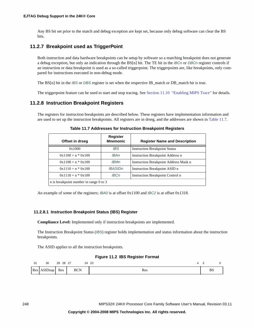
EJTAG Debug Support in the 24K® Core
248 MIPS32® 24K® Processor Core Family Software User’s Manual, Revision 03.11
Copyright © 2004-2008 MIPS Technologies Inc. All rights reserved.
Any BS bit set prior to the match and debug exception are kept set, because only debug software can clear the BSbits.
11.2.7 Breakpoint used as TriggerPoint
Both instruction and data hardware breakpoints can be setup by software so a matching breakpoint does not generatea debug exception, but only an indication through the BS[n] bit. The TE bit in the IBCn or DBCn register controls ifan instruction or data breakpoint is used as a so-called triggerpoint. The triggerpoints are, like breakpoints, only com-pared for instructions executed in non-debug mode.
The BS[n] bit in the IBS or DBS register is set when the respective IB_match or DB_match bit is true.
The triggerpoint feature can be used to start and stop tracing. See Section 11.10 “Enabling MIPS Trace” for details.
11.2.8 Instruction Breakpoint Registers
The registers for instruction breakpoints are described below. These registers have implementation information andare used to set up the instruction breakpoints. All registers are in drseg, and the addresses are shown in Table 11.7.
An example of some of the registers; IBA0 is at offset 0x1100 and IBC2 is at offset 0x1318.
11.2.8.1 Instruction Breakpoint Status (IBS) Register
Compliance Level: Implemented only if instruction breakpoints are implemented.
The Instruction Breakpoint Status (IBS) register holds implementation and status information about the instructionbreakpoints.
The ASID applies to all the instruction breakpoints.
Figure 11.2 IBS Register Format
Table 11.7 Addresses for Instruction Breakpoint Registers
Offset in drsegRegister
Mnemonic Register Name and Description
0x1000 IBS Instruction Breakpoint Status
0x1100 + n * 0x100 IBAn Instruction Breakpoint Address n
0x1108 + n * 0x100 IBMn Instruction Breakpoint Address Mask n
0x1110 + n * 0x100 IBASIDn Instruction Breakpoint ASID n
0x1118 + n * 0x100 IBCn Instruction Breakpoint Control n
n is breakpoint number in range 0 to 3
31 30 29 28 27 24 23 4 3 0
Res ASIDsup Res BCN Res BS

11.2 Hardware Breakpoints
MIPS32® 24K® Processor Core Family Software User’s Manual, Revision 03.11 249
Copyright © 2004-2008 MIPS Technologies Inc. All rights reserved.
11.2.8.2 Instruction Breakpoint Address n (IBAn) Register
Compliance Level: Implemented only for implemented instruction breakpoints.
The Instruction Breakpoint Address n (IBAn) register has the address used in the condition for instruction breakpointn.
Figure 11.3 IBAn Register Format
11.2.8.3 Instruction Breakpoint Address Mask n (IBMn) Register
Compliance Level: Implemented only for implemented instruction breakpoints.
The Instruction Breakpoint Address Mask n (IBMn) register has the mask for the address compare used in the condi-tion for instruction breakpoint n.
Table 11.8 IBS Register Field Descriptions
Fields
DescriptionRead /Write Reset StateName Bit(s)
Res 31 Must be written as zero; returns zero on read. R 0
ASIDsup 30 Indicates that ASID compare is supported in instruction breakpoints.0: No ASID compare.1: ASID compare (IBASIDn register implemented).
1: Supported0: Not supported
R Fixed MMU - 0TLB - 1
Res 29:28 Must be written as zero; returns zero on read. R 0
BCN 27:24 Number of instruction breakpoints implemented. R 4
Res 23:4 Must be written as zero; returns zero on read. R 0
BS 3:0 Break status for breakpoint n is at BS[n], with n from 0 to 3. The bitis set to 1 when the condition for the corresponding breakpoint hasmatched.
R/W Undefined
31 1 0
IBA ISA
Table 11.9 IBAn Register Field Descriptions
Fields
DescriptionRead /Write Reset StateName Bit(s)
IBA 31:1 Instruction breakpoint address for condition. R/W Undefined
ISA 0 Instruction breakpoint ISA mode for condition R/W Undefined

EJTAG Debug Support in the 24K® Core
250 MIPS32® 24K® Processor Core Family Software User’s Manual, Revision 03.11
Copyright © 2004-2008 MIPS Technologies Inc. All rights reserved.
Figure 11.4 IBMn Register Format
11.2.8.4 Instruction Breakpoint ASID n (IBASIDn) Register
Compliance Level: Implemented only for implemented instruction breakpoints.
For processors with a TLB based MMU, this register is used to define an ASID value to be used in the match expres-sion. For cores with a FM MMU, this register is reserved and reads as 0.
Figure 11.5 IBASIDn Register Format
11.2.8.5 Instruction Breakpoint Control n (IBCn) Register
Compliance Level: Implemented only for implemented instruction breakpoints.
The Instruction Breakpoint Control n (IBCn) register controls the setup of instruction breakpoint n.
Figure 11.6 IBCn Register Format
31 1 0
IBM ISAM
Table 11.10 IBMn Register Field Descriptions
Fields
DescriptionRead /Write Reset StateName Bit(s)
IBM 31:1 Instruction breakpoint address mask for condition:0: Corresponding address bit not masked.1: Corresponding address bit masked.
R/W Undefined
ISAM 0 Instruction breakpoint ISA mode mask for condition:0: ISA mode considered for match condition1: ISA mode masked
R/W Undefined
31 8 7 0
Res ASID
Table 11.11 IBASIDn Register Field Descriptions
Fields
DescriptionRead /Write Reset StateName Bit(s)
Res 31:8 Must be written as zero; returns zero on read. R 0
ASID 7:0 Instruction breakpoint ASID value for a compare. R/W Undefined
31 24 23 22 21 3 2 1 0
ResASIDuse
ResRes TE Res BE

11.2 Hardware Breakpoints
MIPS32® 24K® Processor Core Family Software User’s Manual, Revision 03.11 251
Copyright © 2004-2008 MIPS Technologies Inc. All rights reserved.
11.2.9 Data Breakpoint Registers
The registers for data breakpoints are described below. These registers have implementation information and are usedthe setup the data breakpoints. All registers are in drseg, and the addresses are shown in Table 11.13.
An example of some of the registers; DBM0 is at offset 0x2108 and DBV1 is at offset 0x2220.
11.2.9.1 Data Breakpoint Status (DBS) Register
Compliance Level: Implemented if data breakpoints are implemented.
Table 11.12 IBCn Register Field Descriptions
Fields
DescriptionRead /Write Reset StateName Bits
Res 31:24 Must be written as zero; returns zero on read. R 0
ASIDuse 23 Use ASID value in compare for instruction breakpoint n:0: Don’t use ASID value in compare1: Use ASID value in compare
R/W Undefined
Res 22 Must be written as zero; returns zero on read R 0
Res 21:3 Must be written as zero; returns zero on read. R 0
TE 2 Use instruction breakpoint n as triggerpoint:0: Don’t use it as triggerpoint1: Use it as triggerpoint
R/W 0
Res 1 Must be written as zero; returns zero on read. R 0
BE 0 Use instruction breakpoint n as breakpoint:0: Don’t use it as breakpoint1: Use it as breakpoint
R/W 0
Table 11.13 Addresses for Data Breakpoint Registers
Offset in drsegRegister
Mnemonic Register Name and Description
0x2000 DBS Data Breakpoint Status
0x2100 + 0x100 * n DBAn Data Breakpoint Address n
0x2108 + 0x100 * n DBMn Data Breakpoint Address Mask n
0x2110 + 0x100 * n DBASIDn Data Breakpoint ASID n
0x2118 + 0x100 * n DBCn Data Breakpoint Control n
0x2120 + 0x100 * n DBVn Data Breakpoint Value n
0x2124 + 0x100*n DBVHn Data Breakpoint Value High n
n is breakpoint number as 0 or 1

EJTAG Debug Support in the 24K® Core
252 MIPS32® 24K® Processor Core Family Software User’s Manual, Revision 03.11
Copyright © 2004-2008 MIPS Technologies Inc. All rights reserved.
The Data Breakpoint Status (DBS) register holds implementation and status information about the data breakpoints.
The ASIDsup field indicates whether ASID compares are supported.
Figure 11.7 DBS Register Format
11.2.9.2 Data Breakpoint Address n (DBAn) Register
Compliance Level: Implemented only for implemented data breakpoints.
The Data Breakpoint Address n (DBAn) register has the address used in the condition for data breakpoint n.
Figure 11.8 DBAn Register Format
11.2.9.3 Data Breakpoint Address Mask n (DBMn) Register
Compliance Level: Implemented only for implemented data breakpoints.
The Data Breakpoint Address Mask n (DBMn) register has the mask for the address compare used in the condition fordata breakpoint n.
31 30 29 28 27 24 23 2 1 0
Res ASIDsup Res BCN Res BS
Table 11.14 DBS Register Field Descriptions
Fields
DescriptionRead /Write Reset StateName Bit(s)
Res 31 Must be written as zero; returns zero on read. R 0
ASID 30 Indicates that ASID compares are supported in data breakpoints.0: Not supported1: Supported
R TLB MMU - 1FM MMU - 0
Res 29:28 Must be written as zero; returns zero on read. R 0
BCN 27:24 Number of data breakpoints implemented. R 2
Res 23:2 Must be written as zero; returns zero on read. R 0
BS 1:0 Break status for breakpoint n is at BS[n], with n from 0 to 1. The bitis set to 1 when the condition for the corresponding breakpoint hasmatched.
R/W0 Undefined
31 0
DBA
Table 11.15 DBAn Register Field Descriptions
Fields
DescriptionRead /Write Reset StateName Bit(s)
DBA 31:0 Data breakpoint address for condition. R/W Undefined

11.2 Hardware Breakpoints
MIPS32® 24K® Processor Core Family Software User’s Manual, Revision 03.11 253
Copyright © 2004-2008 MIPS Technologies Inc. All rights reserved.
Figure 11.9 DBMn Register Format
11.2.9.4 Data Breakpoint ASID n (DBASIDn) Register
Compliance Level: Implemented only for implemented data breakpoints.
For processors with a TLB based MMU, this register is used to define an ASID value to be used in the match expres-sion. For cores with the FM MMU, this register is reserved and reads as 0.
Figure 11.10 DBASIDn Register Format
11.2.9.5 Data Breakpoint Control n (DBCn) Register
Compliance Level: Implemented only for implemented data breakpoints.
The Data Breakpoint Control n (DBCn) register controls the setup of data breakpoint n.
Figure 11.11 DBCn Register Format
31 0
DBM
Table 11.16 DBMn Register Field Descriptions
Fields
DescriptionRead /Write Reset StateName Bit(s)
DBM 31:0 Data breakpoint address mask for condition:0: Corresponding address bit not masked1: Corresponding address bit masked
R/W Undefined
31 8 7 0
Res ASID
Table 11.17 DBASIDn Register Field Descriptions
Fields
DescriptionRead /Write Reset StateName Bit(s)
Res 31:8 Must be written as zero; returns zero on read. R 0
ASID 7:0 Data breakpoint ASID value for compares. R/W Undefined
31 24 23 22 21 14 13 12 11 4 3 2 1 0
ResASIDuse
ResBAI NoSB NoLB BLM Res TE Res BE

EJTAG Debug Support in the 24K® Core
254 MIPS32® 24K® Processor Core Family Software User’s Manual, Revision 03.11
Copyright © 2004-2008 MIPS Technologies Inc. All rights reserved.
11.2.9.6 Data Breakpoint Value n (DBVn) Register
Compliance Level: Implemented only for implemented data breakpoints.
The Data Breakpoint Value n (DBVn) register has the value used in the condition for data breakpoint n.
Figure 11.12 DBVn Register Format
Table 11.18 DBCn Register Field Descriptions
Fields
DescriptionRead /Write Reset StateName Bits
Res 31:24 Must be written as zero; returns zero on reads. R 0
ASIDuse 23 Use ASID value in compare for data breakpoint n:0: Don’t use ASID value in compare1: Use ASID value in compare
R/W Undefined
Res 22 Must be written as zero; returns zero on reads R 0
BAI 21:14 Byte access ignore controls ignore of access to a specific byte.BAI[0] ignores access to byte at bits [7:0] of the data bus, BAI[1]ignores access to byte at bits [15:8], etc.0: Condition depends on access to corresponding byte1: Access for corresponding byte is ignored
R/W Undefined
NoSB 13 Controls if condition for data breakpoint is not fulfilled on a storetransaction:0: Condition may be fulfilled on store transaction1: Condition is never fulfilled on store transaction
R/W Undefined
NoLB 12 Controls if condition for data breakpoint is not fulfilled on a loadtransaction:0: Condition may be fulfilled on load transaction1: Condition is never fulfilled on load transaction
R/W Undefined
BLM 11:4 Byte lane mask for value compare on data breakpoint. BLM[0]masks byte at bits [7:0] of the data bus, BLM[1] masks byte at bits[15:8], etc.:0: Compare corresponding byte lane1: Mask corresponding byte lane
R/W Undefined
Res 3 Must be written as zero; returns zero on reads. R 0
TE 2 Use data breakpoint n as triggerpoint:0: Don’t use it as triggerpoint1: Use it as triggerpoint
R/W 0
Res 1 Must be written as zero; returns zero on reads. R 0
BE 0 Use data breakpoint n as breakpoint:0: Don’t use it as breakpoint1: Use it as breakpoint
R/W 0
31 0
DBV

11.3 Test Access Port (TAP)
MIPS32® 24K® Processor Core Family Software User’s Manual, Revision 03.11 255
Copyright © 2004-2008 MIPS Technologies Inc. All rights reserved.
11.2.9.7 Data Breakpoint Value High n (DBVHn) Register
Compliance Level: Implemented only for implemented data breakpoints.
The Data Breakpoint Value High n (DBVHn) register has the value used in the condition for data breakpoint n.
Figure 11.13 DBVHn Register Format
11.3 Test Access Port (TAP)
The following main features are supported by the TAP module:
• 5-pin industry standard JTAG Test Access Port (TCK, TMS, TDI, TDO, TRST_N) interface which is compatiblewith IEEE Std. 1149.1.
• Target chip and EJTAG feature identification available through the Test Access Port (TAP) controller.
• The processor can access external memory on the EJTAG Probe serially through the EJTAG pins. This isachieved through Processor Access (PA), and is used to eliminate the use of the system memory for debug rou-tines.
• Support for both ROM based debugger and debugging both through TAP.
Table 11.19 DBVn Register Field Descriptions
Fields
DescriptionRead /Write Reset StateName Bit(s)
DBV 31:0 Data breakpoint value for condition. R/W Undefined
31 0
DBVH
Table 11.20 DBVHn Register Field Descriptions
Fields
DescriptionRead /Write Reset StateName Bit(s)
DBVH 31:0 Data breakpoint value high for condition. This register provides thehigh order bits [63:32] for data value on double-word floating pointloads and stores.
R/W Undefined

EJTAG Debug Support in the 24K® Core
256 MIPS32® 24K® Processor Core Family Software User’s Manual, Revision 03.11
Copyright © 2004-2008 MIPS Technologies Inc. All rights reserved.
11.3.1 EJTAG Internal and External Interfaces
The external interface of the EJTAG module consists of the 5 signals defined by the IEEE standard.
11.3.2 Test Access Port Operation
The TAP controller is controlled by the Test Clock (TCK) and Test Mode Select (TMS) inputs. These two inputsdetermine whether an the Instruction register scan or data register scan is performed. The TAP consists of a smallcontroller, driven by the TCK input, which responds to the TMS input as shown in the state diagram in Figure 11.14.The TAP uses both clock edges of TCK. TMS and TDI are sampled on the rising edge of TCK, while TDO changes onthe falling edge of TCK.
At power-up the TAP is forced into the Test-Logic-Reset by low value on TRST_N. The TAP instruction register isthereby reset to IDCODE. No other parts of the EJTAG hardware are reset through the Test-Logic-Reset state.
When test access is required, a protocol is applied via the TMS and TCK inputs, causing the TAP to exit theTest-Logic-Reset state and move through the appropriate states. From the Run-Test/Idle state, an Instruction registerscan or a data register scan can be issued to transition the TAP through the appropriate states shown in Figure 11.14.
The states of the data and instruction register scan blocks are mirror images of each other adding symmetry to the pro-tocol sequences. The first action that occurs when either block is entered is a capture operation. For the data registers,the Capture-DR state is used to capture (or parallel load) the data into the selected serial data path. In the Instructionregister, the Capture-IR state is used to capture status information into the Instruction register.
Table 11.21 EJTAG Interface Pins
Pin Type Description
TCK I Test Clock InputInput clock used to shift data into or out of the Instruction or data registers. The TCK clock isindependent of the processor clock, so the EJTAG probe can drive TCK independently of theprocessor clock frequency.The core signal for this is called EJ_TCK
TMS I Test Mode Select InputThe TMS input signal is decoded by the TAP controller to control test operation. TMS issampled on the rising edge of TCK.The core signal for this is called EJ_TMS
TDI I Test Data InputSerial input data (TDI) is shifted into the Instruction register or data registers on the risingedge of the TCK clock, depending on the TAP controller state.The core signal for this is called EJ_TDI
TDO O Test Data OutputSerial output data is shifted from the Instruction or data register to the TDO pin on the fallingedge of the TCK clock. When no data is shifted out, the TDO is 3-stated.The core signal for this is called EJ_TDO with output enable controlled by EJ_TDOzstate.
TRST_N I Test Reset Input (Optional pin)The TRST_N pin is an active-low signal for asynchronous reset of the TAP controller andinstruction in the TAP module, independent of the processor logic. The processor is not resetby the assertion of TRST_N.The core signal for this is called EJ_TRST_NThis signal is optional, but power-on reset must apply a low pulse on this signal at power-onand then leave it high, in case the signal is not available as a pin on the chip. If available onthe chip, then it must be low on the board when the EJTAG debug features are unused by theprobe.

11.3 Test Access Port (TAP)
MIPS32® 24K® Processor Core Family Software User’s Manual, Revision 03.11 257
Copyright © 2004-2008 MIPS Technologies Inc. All rights reserved.
From the Capture states, the TAP transitions to either the Shift or Exit1 states. Normally the Shift state follows theCapture state so that test data or status information can be shifted out for inspection and new data shifted in. Follow-ing the Shift state, the TAP either returns to the Run-Test/Idle state via the Exit1 and Update states or enters the Pausestate via Exit1. The reason for entering the Pause state is to temporarily suspend the shifting of data through either theData or Instruction Register while a required operation, such as refilling a host memory buffer, is performed. Fromthe Pause state shifting can resume by re-entering the Shift state via the Exit2 state or terminate by entering theRun-Test/Idle state via the Exit2 and Update states.
Upon entering the data or Instruction register scan blocks, shadow latches in the selected scan path are forced to holdtheir present state during the Capture and Shift operations. The data being shifted into the selected scan path is notoutput through the shadow latch until the TAP enters the Update-DR or Update-IR state. The Update state causes theshadow latches to update (or parallel load) with the new data that has been shifted into the selected scan path.
Figure 11.14 TAP Controller State Diagram
11.3.2.1 Test-Logic-Reset State
In the Test-Logic-Reset state the boundary scan test logic is disabled. The test logic enters the Test-Logic-Reset statewhen the TMS input is held HIGH for at least five rising edges of TCK. The BYPASS instruction is forced into theinstruction register output latches during this state. The controller remains in the Test-Logic-Reset state as long asTMS is HIGH.
11.3.2.2 Run-Test/Idle State
The controller enters the Run-Test/Idle state between scan operations. The controller remains in this state as long asTMS is held LOW. The instruction register and all test data registers retain their previous state. The instruction cannotchange when the TAP controller is in this state.
Shift_IR
Select_IR_Scan
Capture_IR
Exit1_IR
Pause_IR
Exit2_IR
Update_IR
1
0
0
0
0
0
0
1
1
1
1
1
1
1
0
Shift_DR
Select_DR_Scan
Capture_DR
Exit1_DR
Pause_DR
Exit2_DR
Update_DR
0
0
0
0
0
0
1
1
1
1
1
1
1
0
Test-Logic-Reset
Run-Test/Idle
0
1
0
EJTAG Debug Support in the 24K® Core
258 MIPS32® 24K® Processor Core Family Software User’s Manual, Revision 03.11
Copyright © 2004-2008 MIPS Technologies Inc. All rights reserved.
When TMS is sampled HIGH on the rising edge of TCK, the controller transitions to the Select_DR state.
11.3.2.3 Select_DR_Scan State
This is a temporary controller state in which all test data registers selected by the current instruction retain their previ-ous state. If TMS is sampled LOW at the rising edge of TCK, then the controller transitions to the Capture_DR state.A HIGH on TMS causes the controller to transition to the Select_IR state. The instruction cannot change while theTAP controller is in this state.
11.3.2.4 Select_IR_Scan State
This is a temporary controller state in which all test data registers selected by the current instruction retain their previ-ous state. If TMS is sampled LOW on the rising edge of TCK, the controller transitions to the Capture_IR state. AHIGH on TMS causes the controller to transition to the Test-Reset-Logic state. The instruction cannot change whilethe TAP controller is in this state.
11.3.2.5 Capture_DR State
In this state the boundary scan register captures the value of the register addressed by the Instruction register, and thevalue is then shifted out in the Shift_DR. If TMS is sampled LOW at the rising edge of TCK, the controller transitionsto the Shift_DR state. A HIGH on TMS causes the controller to transition to the Exit1_DR state. The instruction can-not change while the TAP controller is in this state.
11.3.2.6 Shift_DR State
In this state the test data register connected between TDI and TDO as a result of the current instruction shifts data onestage toward its serial output on the rising edge of TCK. If TMS is sampled LOW on the rising edge of TCK, the con-troller remains in the Shift_DR state. A HIGH on TMS causes the controller to transition to the Exit1_DR state. Theinstruction cannot change while the TAP controller is in this state.
11.3.2.7 Exit1_DR State
This is a temporary controller state in which all test data registers selected by the current instruction retain their previ-ous state. If TMS is sampled LOW at the rising edge of TCK, the controller transitions to the Pause_DR state. AHIGH on TMS causes the controller to transition to the Update_DR state which terminates the scanning process. Theinstruction cannot change while the TAP controller is in this state.
11.3.2.8 Pause_DR State
The Pause_DR state allows the controller to temporarily halt the shifting of data through the test data register in theserial path between TDI and TDO. All test data registers selected by the current instruction retain their previous state.If TMS is sampled LOW on the rising edge of TCK, the controller remains in the Pause_DR state. A HIGH on TMScauses the controller to transition to the Exit2_DR state. The instruction cannot change while the TAP controller is inthis state.
11.3.2.9 Exit2_DR State
This is a temporary controller state in which all test data registers selected by the current instruction retain their previ-ous state. If TMS is sampled LOW at the rising edge of TCK, the controller transitions to the Shift_DR state to allowanother serial shift of data. A HIGH on TMS causes the controller to transition to the Update_DR state which termi-nates the scanning process. The instruction cannot change while the TAP controller is in this state.

11.3 Test Access Port (TAP)
MIPS32® 24K® Processor Core Family Software User’s Manual, Revision 03.11 259
Copyright © 2004-2008 MIPS Technologies Inc. All rights reserved.
11.3.2.10 Update_DR State
When the TAP controller is in this state the value shifted in during the Shift_DR state takes effect on the rising edgeof the TCK for the register indicated by the Instruction register.
If TMS is sampled LOW at the rising edge of TCK, the controller transitions to the Run-Test/Idle state. A HIGH onTMS causes the controller to transition to the Select_DR_Scan state. The instruction cannot change while the TAPcontroller is in this state and all shift register stages in the test data registers selected by the current instruction retaintheir previous state.
11.3.2.11 Capture_IR State
In this state the shift register contained in the Instruction register loads a fixed pattern (000012) on the rising edge ofTCK. The data registers selected by the current instruction retain their previous state.
If TMS is sampled LOW at the rising edge of TCK, the controller transitions to the Shift_IR state. A HIGH on TMScauses the controller to transition to the Exit1_IR state. The instruction cannot change while the TAP controller is inthis state.
11.3.2.12 Shift_IR State
In this state the instruction register is connected between TDI and TDO and shifts data one stage toward its serial out-put on the rising edge of TCK. If TMS is sampled LOW at the rising edge of TCK, the controller remains in theShift_IR state. A HIGH on TMS causes the controller to transition to the Exit1_IR state.
11.3.2.13 Exit1_IR State
This is a temporary controller state in which all registers retain their previous state. If TMS is sampled LOW at the ris-ing edge of TCK, the controller transitions to the Pause_IR state. A HIGH on TMS causes the controller to transitionto the Update_IR state which terminates the scanning process. The instruction cannot change while the TAP control-ler is in this state and the instruction register retains its previous state.
11.3.2.14 Pause_IR State
The Pause_IR state allows the controller to temporarily halt the shifting of data through the instruction register in theserial path between TDI and TDO. If TMS is sampled LOW at the rising edge of TCK, the controller remains in thePause_IR state. A HIGH on TMS causes the controller to transition to the Exit2_IR state. The instruction cannotchange while the TAP controller is in this state.
11.3.2.15 Exit2_IR State
This is a temporary controller state in which the instruction register retains its previous state. If TMS is sampled LOWat the rising edge of TCK, then the controller transitions to the Shift_IR state to allow another serial shift of data. AHIGH on TMS causes the controller to transition to the Update_IR state which terminates the scanning process. Theinstruction cannot change while the TAP controller is in this state.
11.3.2.16 Update_IR State
The instruction shifted into the instruction register takes effect on the rising edge of TCK.
If TMS is sampled LOW at the rising edge of TCK, the controller transitions to the Run-Test/Idle state. A HIGH onTMS causes the controller to transition to the Select_DR_Scan state.

EJTAG Debug Support in the 24K® Core
260 MIPS32® 24K® Processor Core Family Software User’s Manual, Revision 03.11
Copyright © 2004-2008 MIPS Technologies Inc. All rights reserved.
11.3.3 Test Access Port (TAP) Instructions
The TAP Instruction register allows instructions to be serially input into the device when TAP controller is in theShift-IR state. Instructions are decoded and define the serial test data register path that is used to shift data betweenTDI and TDO during data register scanning.
The Instruction register is a 5-bit register. In the current EJTAG implementation only some instructions have beendecoded; the unused instructions default to the BYPASS instruction.
11.3.3.1 BYPASS Instruction
The required BYPASS instruction allows the processor to remain in a functional mode and selects the Bypass registerto be connected between TDI and TDO. The BYPASS instruction allows serial data to be transferred through the pro-cessor from TDI to TDO without affecting its operation. The bit code of this instruction is defined to be all ones by theIEEE 1149.1 standard. Any unused instruction is defaulted to the BYPASS instruction.
11.3.3.2 IDCODE Instruction
The IDCODE instruction allows the processor to remain in its functional mode and selects the Device Identification(ID) register to be connected between TDI and TDO. The Device ID register is a 32-bit shift register containing infor-mation regarding the IC manufacturer, device type, and version code. Accessing the Identification Register does notinterfere with the operation of the processor. Also, access to the Identification Register is immediately available, via aTAP data scan operation, after power-up when the TAP has been reset with on-chip power-on or through the optionalTRST_N pin.
11.3.3.3 IMPCODE Instruction
This instruction selects the Implementation register for output, which is always 32 bits.
Table 11.22 Implemented EJTAG Instructions
Value Instruction Function
0x01 IDCODE Select Chip Identification data register
0x03 IMPCODE Select Implementation register
0x08 ADDRESS Select Address register
0x09 DATA Select Data register
0x0A CONTROL Select EJTAG Control register
0x0B ALL Select the Address, Data and EJTAG Control registers
0x0C EJTAGBOOT Set EjtagBrk, ProbEn and ProbTrap to 1 as reset value
0x0D NORMALBOOT Set EjtagBrk, ProbEn and ProbTrap to 0 as reset value
0x0E FASTDATA Selects the Data and Fastdata registers
0x10 TCBCONTROLA Selects the TCBTCONTROLA register in the Trace Control Block
0x11 TCBCONTROLB Selects the TCBTCONTROLB register in the Trace Control Block
0x12 TCBDATA Selects the TCBDATA register in the Trace Control Block
0x13 TCBCONTROLC Selects the TCBTCONTROLC register in the Trace Control Block
0x14 PCSAMPLE Selects the PCSAMPLE register
0x1F BYPASS Bypass mode
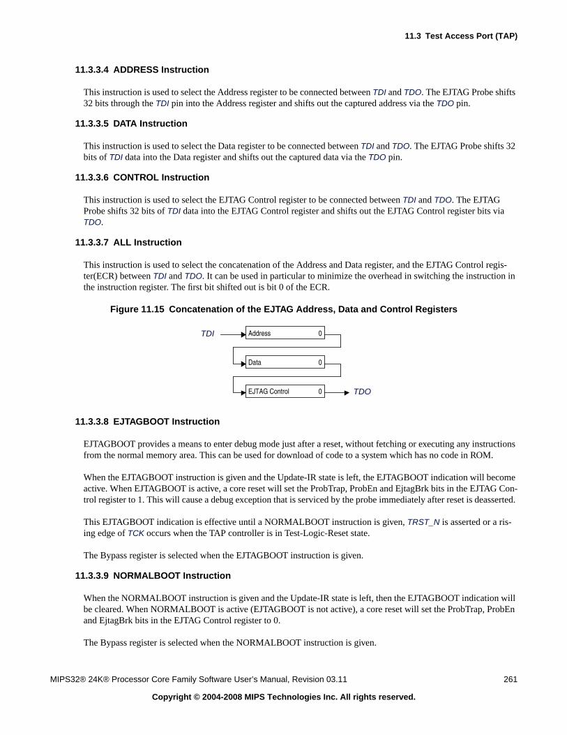
11.3 Test Access Port (TAP)
MIPS32® 24K® Processor Core Family Software User’s Manual, Revision 03.11 261
Copyright © 2004-2008 MIPS Technologies Inc. All rights reserved.
11.3.3.4 ADDRESS Instruction
This instruction is used to select the Address register to be connected between TDI and TDO. The EJTAG Probe shifts32 bits through the TDI pin into the Address register and shifts out the captured address via the TDO pin.
11.3.3.5 DATA Instruction
This instruction is used to select the Data register to be connected between TDI and TDO. The EJTAG Probe shifts 32bits of TDI data into the Data register and shifts out the captured data via the TDO pin.
11.3.3.6 CONTROL Instruction
This instruction is used to select the EJTAG Control register to be connected between TDI and TDO. The EJTAGProbe shifts 32 bits of TDI data into the EJTAG Control register and shifts out the EJTAG Control register bits viaTDO.
11.3.3.7 ALL Instruction
This instruction is used to select the concatenation of the Address and Data register, and the EJTAG Control regis-ter(ECR) between TDI and TDO. It can be used in particular to minimize the overhead in switching the instruction inthe instruction register. The first bit shifted out is bit 0 of the ECR.
Figure 11.15 Concatenation of the EJTAG Address, Data and Control Registers
11.3.3.8 EJTAGBOOT Instruction
EJTAGBOOT provides a means to enter debug mode just after a reset, without fetching or executing any instructionsfrom the normal memory area. This can be used for download of code to a system which has no code in ROM.
When the EJTAGBOOT instruction is given and the Update-IR state is left, the EJTAGBOOT indication will becomeactive. When EJTAGBOOT is active, a core reset will set the ProbTrap, ProbEn and EjtagBrk bits in the EJTAG Con-trol register to 1. This will cause a debug exception that is serviced by the probe immediately after reset is deasserted.
This EJTAGBOOT indication is effective until a NORMALBOOT instruction is given, TRST_N is asserted or a ris-ing edge of TCK occurs when the TAP controller is in Test-Logic-Reset state.
The Bypass register is selected when the EJTAGBOOT instruction is given.
11.3.3.9 NORMALBOOT Instruction
When the NORMALBOOT instruction is given and the Update-IR state is left, then the EJTAGBOOT indication willbe cleared. When NORMALBOOT is active (EJTAGBOOT is not active), a core reset will set the ProbTrap, ProbEnand EjtagBrk bits in the EJTAG Control register to 0.
The Bypass register is selected when the NORMALBOOT instruction is given.
Address 0
Data 0
EJTAG Control 0 TDO
TDI

EJTAG Debug Support in the 24K® Core
262 MIPS32® 24K® Processor Core Family Software User’s Manual, Revision 03.11
Copyright © 2004-2008 MIPS Technologies Inc. All rights reserved.
11.3.3.10 FASTDATA Instruction
This selects the Data and the Fastdata registers at once, as shown in Figure 11.16.
Figure 11.16 TDI to TDO Path When in Shift-DR State and FASTDATA Instruction is Selected
11.3.3.11 TCBCONTROLA Instruction
This instruction is used to select the TCBCONTROLA register to be connected between TDI and TDO. This registeris only implemented if the Trace Control Block is present. If no TCB is present, then this instruction will select theBypass register.
11.3.3.12 TCBCONTROLB Instruction
This instruction is used to select the TCBCONTROLB register to be connected between TDI and TDO. This register isonly implemented if the Trace Control Block is present. If no TCB is present, then this instruction will select theBypass register.
11.3.3.13 TCBCONTROLC Instruction
This instruction is used to select the TCBCONTROLC register to be connected between TDI and TDO. This register isonly implemented if the Trace Control Block is present. If no TCB is present, then this instruction will select theBypass register.
11.3.3.14 TCBDATA Instruction
This instruction is used to select the TCBDATA register to be connected between TDI and TDO. This register is onlyimplemented if the Trace Control Block is present. If no TCB is present, then this instruction will select the Bypassregister. It should be noted that the TCBDATA register is only an access register to other TCB registers. The width ofthe TCBDATA register is dependent on the specific TCB register.
11.3.3.15 PCSAMPLE Instruction
This instruction is used to select the PCSAMPLE register to be connected between TDI and TDO. This register isalways implemented.
11.4 EJTAG TAP Registers
The EJTAG TAP Module has one Instruction register and a number of data registers, all accessible through the TAP:
11.4.1 Instruction Register
The Instruction register is accessed when the TAP receives an Instruction register scan protocol. During an Instruc-tion register scan operation the TAP controller selects the output of the Instruction register to drive the TDO pin. Theshift register consists of a series of bits arranged to form a single scan path between TDI and TDO. During an Instruc-tion register scan operations, the TAP controls the register to capture status information and shift data from TDI toTDO. Both the capture and shift operations occur on the rising edge of TCK. However, the data shifted out from theTDO occurs on the falling edge of TCK. In the Test-Logic-Reset and Capture-IR state, the instruction shift register is
TDI Data TDOFastdata0

11.4 EJTAG TAP Registers
MIPS32® 24K® Processor Core Family Software User’s Manual, Revision 03.11 263
Copyright © 2004-2008 MIPS Technologies Inc. All rights reserved.
set to 000012, as for the IDCODE instruction. This forces the device into the functional mode and selects the DeviceID register. The Instruction register is 5 bits wide. The instruction shifted in takes effect for the following data regis-ter scan operation. A list of the implemented instructions are listed in Table 11.22.
11.4.2 Data Registers Overview
The EJTAG uses several data registers, which are arranged in parallel from the primary TDI input to the primary TDOoutput. The Instruction register supplies the address that allows one of the data registers to be accessed during a dataregister scan operation. During a data register scan operation, the addressed scan register receives TAP control sig-nals to capture the register and shift data from TDI to TDO. During a data register scan operation, the TAP selects theoutput of the data register to drive the TDO pin. The register is updated in the Update-DR state with respect to thewrite bits.
This description applies in general to the following data registers:
• Bypass Register
• Device Identification Register
• Implementation Register
• EJTAG Control Register (ECR)
• Processor Access Address Register
• Processor Access Data Register
• FastData Register
11.4.2.1 Bypass Register
The Bypass register consists of a single scan register bit. When selected, the Bypass register provides a single bit scanpath between TDI and TDO. The Bypass register allows abbreviating the scan path through devices that are notinvolved in the test. The Bypass register is selected when the Instruction register is loaded with a pattern of all ones tosatisfy the IEEE 1149.1 Bypass instruction requirement.
11.4.2.2 Device Identification (ID) Register
The Device Identification register is defined by IEEE 1149.1, to identify the device's manufacturer, part number, revi-sion, and other device-specific information. Table 11.23 shows the bit assignments defined for the read-only DeviceIdentification Register, and inputs to the core determine the value of these bits. These bits can be scanned out of the IDregister after being selected. The register is selected when the Instruction register is loaded with the IDCODE instruc-tion.
Figure 11.17 Device Identification Register Format31 28 27 12 11 1 0
Version PartNumber ManufID R

EJTAG Debug Support in the 24K® Core
264 MIPS32® 24K® Processor Core Family Software User’s Manual, Revision 03.11
Copyright © 2004-2008 MIPS Technologies Inc. All rights reserved.
11.4.2.3 Implementation Register
This 32-bit read-only register is used to identify the features of the EJTAG implementation. Some of the reset valuesare set by inputs to the core. The register is selected when the Instruction register is loaded with the IMPCODEinstruction.
Figure 11.18 Implementation Register Format
Table 11.23 Device Identification Register
Fields
DescriptionRead /Write Reset StateName Bit(s)
Version 31:28 Version (4 bits)This field identifies the version number of the processorderivative.
R EJ_Version[3:0]
PartNumber 27:12 Part Number (16 bits)This field identifies the part number of the processorderivative.
R EJ_PartNumber[15:0]
ManufID 11:1 Manufacturer Identity (11 bits)Accordingly to IEEE 1149.1-1990, the manufacturer iden-tity code shall be a compressed form of the JEDEC Publi-cations 106-A.
R EJ_ManufID[10:0]
R 0 reserved R 1
31 29 28 25 24 23 21 20 17 16 15 14 13 0
EJTAGver reserved DINTsup ASIDsize reserved MIPS16 0 NoDMA reserved
Table 11.24 Implementation Register Descriptions
Fields
DescriptionRead /Write Reset StateName Bit(s)
EJTAGver 31:29 EJTAG Version.3: Version 3.1
R 3
reserved 28:25 reserved R 0
DINTsup 24 DINT Signal Supported from ProbeThis bit indicates if the DINT signal from the probe is supported:0: DINT signal from the probe is not supported1: Probe can use DINT signal to make debug interrupt.
R EJ_DINTsup
ASIDsize 23:21 Size of ASID field in implementation:0: No ASID in implementation2: 8-bit ASID1,3: Reserved
R TLB MMU- 2FM MMU- 0
reserved 20:17 reserved R 0
MIPS16 16 Indicates whether MIPS16 is implemented0: No MIPS16 support1: MIPS16 implemented
R 1
reserved 15 reserved R 0
NoDMA 14 No EJTAG DMA Support R 1
reserved 13:0 reserved R 0

11.4 EJTAG TAP Registers
MIPS32® 24K® Processor Core Family Software User’s Manual, Revision 03.11 265
Copyright © 2004-2008 MIPS Technologies Inc. All rights reserved.
11.4.2.4 EJTAG Control Register
This 32-bit register controls the various operations of the TAP modules. This register is selected by shifting in theCONTROL instruction. Bits in the EJTAG Control register can be set/cleared by shifting in data; status is read byshifting out the contents of this register. This EJTAG Control register can only be accessed by the TAP interface.
The EJTAG Control register is not updated in the Update-DR state unless the Reset occurred (Rocc) bit 31, is either 0or written to 0. This is in order to ensure prober handling of processor accesses.
The value used for reset indicated in the table below takes effect on CPU resets, but not on TAP controller resets bye.g. TRST_N. TCK clock is not required when the CPU reset occurs, but the bits are still updated to the reset valuewhen the TCK applies. The first 5 TCK clocks after CPU resets may result in reset of the bits, due to synchronizationbetween clock domains.
Figure 11.19 EJTAG Control Register Format31 30 29 28 24 23 22 21 20 19 18 17 16 15 14 13 12 11 4 3 2 0
Rocc Psz Res Res Doze Halt PerRst PRnW PrAcc Res PrRst ProbEn ProbTrap Res EjtagBrk Res DM Res
Table 11.25 EJTAG Control Register Descriptions
Fields
DescriptionRead /Write Reset StateName Bit(s)
Rocc 31 Reset OccurredThe bit indicates if a CPU reset has occurred:0: No reset occurred since bit last cleared.1: Reset occurred since bit last cleared.The Rocc bit will keep the 1 value as long as reset is applied.This bit must be cleared by the probe, t Ô(knowledge that the inci-dent was detected.The EJTAG Control register is not updated in the Update-DR stateunless Rocc is 0, or written to 0. This is in order to ensure properhandling of processor access.
R/W 1

EJTAG Debug Support in the 24K® Core
266 MIPS32® 24K® Processor Core Family Software User’s Manual, Revision 03.11
Copyright © 2004-2008 MIPS Technologies Inc. All rights reserved.
Psz[1:0] 30:29 Processor Access Transfer SizeThese bits are used in combination with the lower two address bitsof the Address register to determine the size of a processor accesstransaction. The bits are only valid when processor access is pend-ing.
Note: LE=little endian, BE=big endian, the byte# refers to the bytenumber in a 32-bit register, where byte 3 = bits 31:24; byte 2 = bits23:16; byte 1 = bits 15:8; byte 0=bits 7:0, independently of the endi-aness.
R Undefined
Res 28:24 reserved R 0
Res 23 reserved R 0
Doze 22 Doze stateThe Doze bit indicates any kind of low power mode. The value issampled in the Capture-DR state of the TAP controller:0: CPU not in low power mode.1: CPU is in low power modeDoze includes the Reduced Power (RP) and WAIT power-reductionmodes.
R 0
Halt 21 Halt stateThe Halt bit indicates if the internal system bus clock is running orstopped. The value is sampled in the Capture-DR state of the TAPcontroller:0: Internal system clock is running1: Internal system clock is stopped
R 0
Table 11.25 EJTAG Control Register Descriptions (Continued)
Fields
DescriptionRead /Write Reset StateName Bit(s)
PAA[1:0] Psz[1:0] Transfer Size
00 00 Byte (LE, byte 0; BE, byte 3)
01 00 Byte (LE, byte 1; BE, byte 2)
10 00 Byte (LE, byte 2; BE, byte 1)
11 00 Byte (LE, byte 3; BE, byte 0)
00 01 Halfword (LE, bytes 1:0; BE, bytes 3:2)
10 01 Halfword (LE, bytes 3:2; BE, bytes 1:0)
00 10 Word (LE, BE; bytes 3, 2, 1, 0)
00 11 Triple (LE, bytes 2, 1, 0; BE, bytes 3,2,1)
01 11 Triple (LE, bytes 3, 2, 1; BE, bytes 2, 1,0)
All others Reserved

11.4 EJTAG TAP Registers
MIPS32® 24K® Processor Core Family Software User’s Manual, Revision 03.11 267
Copyright © 2004-2008 MIPS Technologies Inc. All rights reserved.
PerRst 20 Peripheral ResetWhen the bit is set to 1, it is only guaranteed that the peripheral resethas occurred in the system when the read value of this bit is also 1.This is to ensure that the setting from the TCK clock domain getseffect in the CPU clock domain, and in peripherals.When the bit is written to 0, then the bit must also be read as 0before it is guaranteed that the indication is cleared in the CPU clockdomain also.This bit controls the EJ_PerRst signal on the core.
R/W 0
PRnW 19 Processor Access Read and WriteThis bit indicates if the pending processor access is for a read orwrite transaction, and the bit is only valid while PrAcc is set:0: Read transaction1: Write transaction
R Undefined
PrAcc 18 Processor Access (PA)Read value of this bit indicates if a Processor Access (PA) to theEJTAG memory is pending:0: No pending processor access1: Pending processor accessThe probe’s software must clear this bit to 0 to indicate the end ofthe PA. Write of 1 is ignored.A pending Processor Access is cleared when Rocc is set, but anotherPA may occur just after the reset if a debug exception occurs.Finishing a Processor Access is not accepted while the Rocc bit isset. This is to avoid that a Processor Access occurring after the resetis finished due to indication of a Processor Access that occurredbefore the reset.The FASTDATA access can clear this bit.
R/W0 0
Res 17 reserved R 0
PrRst 16 Processor Reset (Implementation dependent behavior)When the bit is set to 1, then it is only guaranteed that this settinghas taken effect in the system when the read value of this bit is also1. This is to ensure that the setting from the TCK clock domain getseffect in the CPU clock domain, and in peripherals.When the bit is written to 0, then the bit must also be read as 0before it is guaranteed that the indication is cleared in the CPU clockdomain also.This bit controls the EJ_PrRst signal. If the signal is used in thesystem, then it must be ensured that both the processor and alldevices required for a reset are properly reset. Otherwise the systemmay fail or hang. The bit resets itself, since the EJTAG Control reg-ister is reset by a reset.
R/W 0
Table 11.25 EJTAG Control Register Descriptions (Continued)
Fields
DescriptionRead /Write Reset StateName Bit(s)

EJTAG Debug Support in the 24K® Core
268 MIPS32® 24K® Processor Core Family Software User’s Manual, Revision 03.11
Copyright © 2004-2008 MIPS Technologies Inc. All rights reserved.
ProbEn 15 Probe EnableThis bit indicates to the CPU if the EJTAG memory is handled bythe probe so processor accesses are answered:0: The probe does not handle EJTAG memory transactions1: The probe does handle EJTAG memory transactionsIt is an error by the software controlling the probe if it sets the Prob-Trap bit to 1, but resets the ProbEn to 0. The operation of the proces-sor is UNDEFINED in this case.The ProbEn bit is reflected as a read-only bit in the ProbEn bit, bit 0,in the Debug Control Register (DCR).The read value indicates the effective value in the DCR, due to syn-chronization issues between TCK and CPU clock domains; how-ever, it is ensured that change of the ProbEn prior to setting theEjtagBrk bit will have effect for the debug handler executed due tothe debug exception.The reset value of the bit depends on whether the EJTAGBOOTindication is given or not:No EJTAGBOOT indication given: 0EJTAGBOOT indication given: 1
R/W 0 or 1from
EJTAGBOOT
ProbTrap 14 Probe TrapThis bit controls the location of the debug exception vector:0: In normal memory 0xBFC0.04801: In EJTAG memory at 0xFF20.0200 in dmsegValid setting of the ProbTrap bit depends on the setting of theProbEn bit, see comment under ProbEn bit.The ProbTrap should not be set to 1, for debug exception vector inEJTAG memory, unless the ProbEn bit is also set to 1 to indicatethat the EJTAG memory may be accessed.The read value indicates the effective value to the CPU, due to syn-chronization issues between TCK and CPU clock domains; how-ever, it is ensured that change of the ProbTrap bit prior to setting theEjtagBrk bit will have effect for the EjtagBrk.The reset value of the bit depends on whether the EJTAGBOOTindication is given or not:No EJTAGBOOT indication given: 0EJTAGBOOT indication given: 1
R/W 0 or 1from
EJTAGBOOT
Res 13 reserved R 0
EjtagBrk 12 EJTAG BreakSetting this bit to 1 causes a debug exception to the processor, unlessthe CPU was in debug mode or another debug exception occurred.When the debug exception occurs, the processor core clock isrestarted if the CPU was in low power mode. This bit is cleared byhardware when the debug exception is taken.
The reset value of the bit depends on whether the EJTAGBOOTindication is given or not:No EJTAGBOOT indication given: 0EJTAGBOOT indication given: 1
R/W 0 or 1from
EJTAGBOOT
Res 11:4 reserved R 0
Table 11.25 EJTAG Control Register Descriptions (Continued)
Fields
DescriptionRead /Write Reset StateName Bit(s)
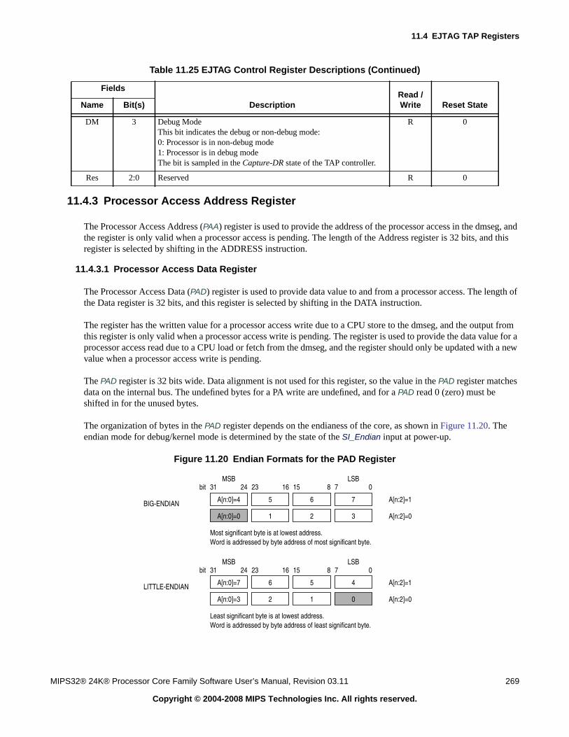
11.4 EJTAG TAP Registers
MIPS32® 24K® Processor Core Family Software User’s Manual, Revision 03.11 269
Copyright © 2004-2008 MIPS Technologies Inc. All rights reserved.
11.4.3 Processor Access Address Register
The Processor Access Address (PAA) register is used to provide the address of the processor access in the dmseg, andthe register is only valid when a processor access is pending. The length of the Address register is 32 bits, and thisregister is selected by shifting in the ADDRESS instruction.
11.4.3.1 Processor Access Data Register
The Processor Access Data (PAD) register is used to provide data value to and from a processor access. The length ofthe Data register is 32 bits, and this register is selected by shifting in the DATA instruction.
The register has the written value for a processor access write due to a CPU store to the dmseg, and the output fromthis register is only valid when a processor access write is pending. The register is used to provide the data value for aprocessor access read due to a CPU load or fetch from the dmseg, and the register should only be updated with a newvalue when a processor access write is pending.
The PAD register is 32 bits wide. Data alignment is not used for this register, so the value in the PAD register matchesdata on the internal bus. The undefined bytes for a PA write are undefined, and for a PAD read 0 (zero) must beshifted in for the unused bytes.
The organization of bytes in the PAD register depends on the endianess of the core, as shown in Figure 11.20. Theendian mode for debug/kernel mode is determined by the state of the SI_Endian input at power-up.
Figure 11.20 Endian Formats for the PAD Register
DM 3 Debug ModeThis bit indicates the debug or non-debug mode:0: Processor is in non-debug mode1: Processor is in debug modeThe bit is sampled in the Capture-DR state of the TAP controller.
R 0
Res 2:0 Reserved R 0
Table 11.25 EJTAG Control Register Descriptions (Continued)
Fields
DescriptionRead /Write Reset StateName Bit(s)
A[n:0]=7 6 5 4
012A[n:0]=3
A[n:0]=4 5 6 7
321A[n:0]=0
0781516232431
0781516232431
LSBbit
MSB
LSBbit
MSB
A[n:2]=1
A[n:2]=0
A[n:2]=1
A[n:2]=0
Most significant byte is at lowest address.Word is addressed by byte address of most significant byte.
BIG-ENDIAN
LITTLE-ENDIAN
Least significant byte is at lowest address.Word is addressed by byte address of least significant byte.

EJTAG Debug Support in the 24K® Core
270 MIPS32® 24K® Processor Core Family Software User’s Manual, Revision 03.11
Copyright © 2004-2008 MIPS Technologies Inc. All rights reserved.
The size of the transaction and thus the number of bytes available/required for the PAD register is determined by thePsz field in the ECR.
11.4.4 Fastdata Register (TAP Instruction FASTDATA)
The width of the Fastdata register is 1 bit. During a Fastdata access, the Fastdata register is written and read, i.e., a bitis shifted in and a bit is shifted out. During a Fastdata access, the Fastdata register value shifted in specifies whetherthe Fastdata access should be completed or not. The value shifted out is a flag that indicates whether the Fastdataaccess was successful or not (if completion was requested).
Figure 11.21 Fastdata Register Format
The FASTDATA access is used for efficient block transfers between dmseg (on the probe) and target memory (on theprocessor). An “upload” is defined as a sequence of processor loads from target memory and stores to dmseg. A“download” is a sequence of processor loads from dmseg and stores to target memory. The “Fastdata area” specifiesthe legal range of dmseg addresses (0xFF20.0000 - 0xFF20.000F) that can be used for uploads and downloads. TheData + Fastdata registers (selected with the FASTDATA instruction) allow efficient completion of pending Fastdataarea accesses.
During Fastdata uploads and downloads, the processor will stall on accesses to the Fastdata area. The PrAcc (proces-sor access pending bit) will be 1 indicating the probe is required to complete the access. Both upload and downloadaccesses are attempted by shifting in a zero SPrAcc value (to request access completion) and shifting out SPrAcc tosee if the attempt will be successful (i.e., there was an access pending and a legal Fastdata area address was used).Downloads will also shift in the data to be used to satisfy the load from dmseg’s Fastdata area, while uploads willshift out the data being stored to dmseg’s Fastdata area.
As noted above, two conditions must be true for the Fastdata access to succeed. These are:
• PrAcc must be 1, i.e., there must be a pending processor access.
• The Fastdata operation must use a valid Fastdata area address in dmseg (0xFF20.0000 to 0xFF20.000F).
0
SPrAcc
Table 11.26 Fastdata Register Field Description
Fields
DescriptionRead /Write
Power-upStateName Bits
SPrAcc 0 Shifting in a zero value requests completion of the Fastdata access.The PrAcc bit in the EJTAG Control register is overwritten withzero when the access succeeds. (The access succeeds if PrAcc isone and the operation address is in the legal dmseg Fastdata area.)When successful, a one is shifted out. Shifting out a zero indicatesa Fastdata access failure.Shifting in a one does not complete the Fastdata access and thePrAcc bit is unchanged. Shifting out a one indicates that the accesswould have been successful if allowed to complete and a zero indi-cates the access would not have successfully completed.
R/W Undefined
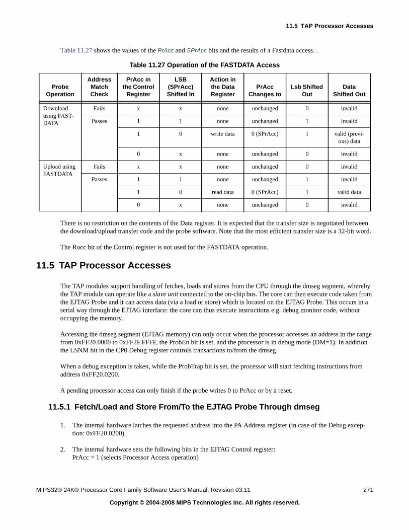
11.5 TAP Processor Accesses
MIPS32® 24K® Processor Core Family Software User’s Manual, Revision 03.11 271
Copyright © 2004-2008 MIPS Technologies Inc. All rights reserved.
Table 11.27 shows the values of the PrAcc and SPrAcc bits and the results of a Fastdata access. .
There is no restriction on the contents of the Data register. It is expected that the transfer size is negotiated betweenthe download/upload transfer code and the probe software. Note that the most efficient transfer size is a 32-bit word.
The Rocc bit of the Control register is not used for the FASTDATA operation.
11.5 TAP Processor Accesses
The TAP modules support handling of fetches, loads and stores from the CPU through the dmseg segment, wherebythe TAP module can operate like a slave unit connected to the on-chip bus. The core can then execute code taken fromthe EJTAG Probe and it can access data (via a load or store) which is located on the EJTAG Probe. This occurs in aserial way through the EJTAG interface: the core can thus execute instructions e.g. debug monitor code, withoutoccupying the memory.
Accessing the dmseg segment (EJTAG memory) can only occur when the processor accesses an address in the rangefrom 0xFF20.0000 to 0xFF2F.FFFF, the ProbEn bit is set, and the processor is in debug mode (DM=1). In additionthe LSNM bit in the CP0 Debug register controls transactions to/from the dmseg.
When a debug exception is taken, while the ProbTrap bit is set, the processor will start fetching instructions fromaddress 0xFF20.0200.
A pending processor access can only finish if the probe writes 0 to PrAcc or by a reset.
11.5.1 Fetch/Load and Store From/To the EJTAG Probe Through dmseg
1. The internal hardware latches the requested address into the PA Address register (in case of the Debug excep-tion: 0xFF20.0200).
2. The internal hardware sets the following bits in the EJTAG Control register:PrAcc = 1 (selects Processor Access operation)
Table 11.27 Operation of the FASTDATA Access
ProbeOperation
AddressMatchCheck
PrAcc inthe Control
Register
LSB(SPrAcc)Shifted In
Action inthe DataRegister
PrAccChanges to
Lsb ShiftedOut
DataShifted Out
Downloadusing FAST-DATA
Fails x x none unchanged 0 invalid
Passes 1 1 none unchanged 1 invalid
1 0 write data 0 (SPrAcc) 1 valid (previ-ous) data
0 x none unchanged 0 invalid
Upload usingFASTDATA
Fails x x none unchanged 0 invalid
Passes 1 1 none unchanged 1 invalid
1 0 read data 0 (SPrAcc) 1 valid data
0 x none unchanged 0 invalid

EJTAG Debug Support in the 24K® Core
272 MIPS32® 24K® Processor Core Family Software User’s Manual, Revision 03.11
Copyright © 2004-2008 MIPS Technologies Inc. All rights reserved.
PRnW = 0 (selects processor read operation)Psz[1:0] = value depending on the transfer size
3. The EJTAG Probe selects the EJTAG Control register, shifts out this control register’s data and tests the PrAccstatus bit (Processor Access): when the PrAcc bit is found 1, it means that the requested address is available andcan be shifted out.
4. The EJTAG Probe checks the PRnW bit to determine the required access.
5. The EJTAG Probe selects the PA Address register and shifts out the requested address.
6. The EJTAG Probe selects the PA Data register and shifts in the instruction corresponding to this address.
7. The EJTAG Probe selects the EJTAG Control register and shifts a PrAcc = 0 bit into this register to indicate tothe processor that the instruction is available.
8. The instruction becomes available in the instruction register and the processor starts executing.
9. The processor increments the program counter and outputs an instruction read request for the next instruction.This starts the whole sequence again.
Using the same protocol, the processor can also execute a load instruction to access the EJTAG Probe’s memory. Forthis to happen, the processor must execute a load instruction (e.g. a LW, LH, LB) with the target address in the appro-priate range.
Almost the same protocol is used to execute a store instruction to the EJTAG Probe’s memory through dmseg. Thestore address must be in the range: 0xFF20.0000 to 0xFF2F.FFFF, the ProbEn bit must be set and the processor has tobe in debug mode (DM=1). The sequence of actions is found below:
1. The internal hardware latches the requested address into the PA Address register
2. The internal hardware latches the data to be written into the PA Data register.
3. The internal hardware sets the following bits in the EJTAG Control register:PrAcc = 1 (selects Processor Access operation)PRnW = 1 (selects processor write operation)Psz[1:0] = value depending on the transfer size
4. The EJTAG Probe selects the EJTAG Control register, shifts out this control register’s data and tests the PrAccstatus bit (Processor Access): when the PrAcc bit is found 1, it means that the requested address is available andcan be shifted out.
5. The EJTAG Probe checks the PRnW bit to determine the required access.
6. The EJTAG Probe selects the PA Address register and shifts out the requested address.
7. The EJTAG Probe selects the PA Data register and shifts out the data to be written.
8. The EJTAG Probe selects the EJTAG Control register and shifts a PrAcc = 0 bit into this register to indicate tothe processor that the write access is finished.
9. The EJTAG Probe writes the data to the requested address in its memory.
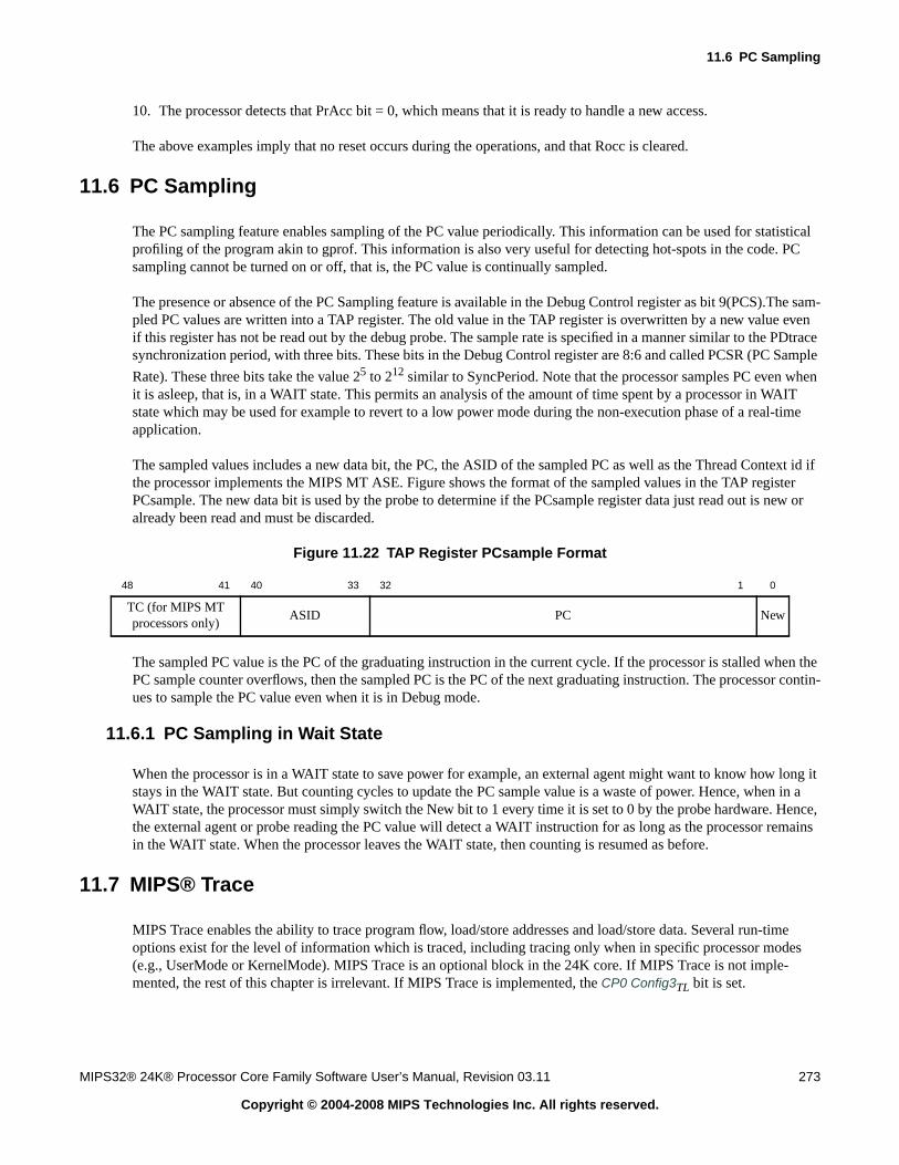
11.6 PC Sampling
MIPS32® 24K® Processor Core Family Software User’s Manual, Revision 03.11 273
Copyright © 2004-2008 MIPS Technologies Inc. All rights reserved.
10. The processor detects that PrAcc bit = 0, which means that it is ready to handle a new access.
The above examples imply that no reset occurs during the operations, and that Rocc is cleared.
11.6 PC Sampling
The PC sampling feature enables sampling of the PC value periodically. This information can be used for statisticalprofiling of the program akin to gprof. This information is also very useful for detecting hot-spots in the code. PCsampling cannot be turned on or off, that is, the PC value is continually sampled.
The presence or absence of the PC Sampling feature is available in the Debug Control register as bit 9(PCS).The sam-pled PC values are written into a TAP register. The old value in the TAP register is overwritten by a new value evenif this register has not be read out by the debug probe. The sample rate is specified in a manner similar to the PDtracesynchronization period, with three bits. These bits in the Debug Control register are 8:6 and called PCSR (PC Sample
Rate). These three bits take the value 25 to 212 similar to SyncPeriod. Note that the processor samples PC even whenit is asleep, that is, in a WAIT state. This permits an analysis of the amount of time spent by a processor in WAITstate which may be used for example to revert to a low power mode during the non-execution phase of a real-timeapplication.
The sampled values includes a new data bit, the PC, the ASID of the sampled PC as well as the Thread Context id ifthe processor implements the MIPS MT ASE. Figure shows the format of the sampled values in the TAP registerPCsample. The new data bit is used by the probe to determine if the PCsample register data just read out is new oralready been read and must be discarded.
Figure 11.22 TAP Register PCsample Format
The sampled PC value is the PC of the graduating instruction in the current cycle. If the processor is stalled when thePC sample counter overflows, then the sampled PC is the PC of the next graduating instruction. The processor contin-ues to sample the PC value even when it is in Debug mode.
11.6.1 PC Sampling in Wait State
When the processor is in a WAIT state to save power for example, an external agent might want to know how long itstays in the WAIT state. But counting cycles to update the PC sample value is a waste of power. Hence, when in aWAIT state, the processor must simply switch the New bit to 1 every time it is set to 0 by the probe hardware. Hence,the external agent or probe reading the PC value will detect a WAIT instruction for as long as the processor remainsin the WAIT state. When the processor leaves the WAIT state, then counting is resumed as before.
11.7 MIPS® Trace
MIPS Trace enables the ability to trace program flow, load/store addresses and load/store data. Several run-timeoptions exist for the level of information which is traced, including tracing only when in specific processor modes(e.g., UserMode or KernelMode). MIPS Trace is an optional block in the 24K core. If MIPS Trace is not imple-mented, the rest of this chapter is irrelevant. If MIPS Trace is implemented, the CP0 Config3TL bit is set.
48 41 40 33 32 1 0
TC (for MIPS MTprocessors only)
ASID PC New

EJTAG Debug Support in the 24K® Core
274 MIPS32® 24K® Processor Core Family Software User’s Manual, Revision 03.11
Copyright © 2004-2008 MIPS Technologies Inc. All rights reserved.
There are two primary blocks involved in the MIPS Trace solution. The pipeline specific part of MIPS Trace is calledthe PDtrace module. It extracts the trace information from the processor pipeline, and presents it to a pipeline-inde-pendent module called the Trace Control Block (TCB). The TCB and the interface between the two blocks (PDtraceinterface) are described in The PDtrace™ Interface and Trace Control Block Specification [9] While working closelytogether, the two parts of MIPS Trace are controlled separately by software. Figure 11.23 shows an overview of theMIPS Trace modules within the core.
Figure 11.23 MIPS® Trace Modules in the 24K® Core
To some extent, the two modules both provide similar trace control features, but the access to these features is quitedifferent. The PDtrace controls can only be reached through access to CP0 registers. The TCB controls can only bereached through EJTAG TAP access. The TCB can then control what is traced through the PDtrace™ Interface.
Before describing the MIPS Trace implemented in the 24K core, some common terminology and basic features areexplained. The remaining sections of this chapter will then provide a more thorough explanation.
11.7.1 Processor Modes
Tracing can be enabled or disabled based on various processor modes. This section precisely describes these modes.The terminology is then used elsewhere in the document.
DebugMode ← (DebugDM = 1)ExceptionMode ← (not DebugMode) and ((StatusEXL = 1) or (StatusERL = 1))KernelMode ← (not (DebugMode or ExceptionMode)) and (StatusKSU = 2#00)SupervisorMode ← (not (DebugMode or ExceptionMode)) and (StatusKSU = 2#01)UserMode ← (not (DebugMode or ExceptionMode)) and (StatusKSU = 2#10)
11.7.2 Software Versus Hardware Control
In some of the specifications and in this text, the terms “software control” and “hardware control” are used to refer tothe method for how trace is controlled. Software control is when the CP0 register TraceControl is used to select themodes to trace, etc. Hardware control is when the EJTAG register TCBCONTROLA in the TCB, via the PDtrace inter-face, is used to select the trace modes. The TraceControlTS bit determines whether software or hardware control isactive. Even in Software control mode, Trace logic will need TCK to toggle atleast once before it is turned on. It isassumed that EJTAG probe will be connected while using Trace and probe reset sequence would toggle TCK. Inorder to extract Trace data out of TCB, TCBCONTROLB.En should be set to 1 even in “software control” mode.
Pipeline specific PDtrace™module
Pipeline independantTrace Contol Block (TCB) modulePDtrace™ Interface
Control pathCP0 control bus EJTAG TAP access
Extracted Pipelineinformation
Back-stall topipeline
On-chip TraceMemory (optional)
TraceProbe
24K boundary(tpz_top)
Tracecompression and
alignmentTrace
extraction
TAPProbe

11.7 MIPS® Trace
MIPS32® 24K® Processor Core Family Software User’s Manual, Revision 03.11 275
Copyright © 2004-2008 MIPS Technologies Inc. All rights reserved.
11.7.3 Trace Information
The main object of trace is to show the exact program flow from a specific program execution or just a small windowof the execution. In MIPS Trace this is done by providing the minimal cycle-by-cycle information necessary on thePDtrace™ interface for trace regeneration software to reproduce the trace. The following is a summary of the type ofinformation traced:
• Only instructions which complete at the end of the pipeline are traced, and indicated with a completion-flag.The PC is implicitly pointing to the next instruction.
• Load instructions are indicated with a load-flag.
• Store instructions are indicated with a store-flag1.
• Taken branches are indicated with a branch-taken-flag on the target instruction.
• New PC information for a branch is only traced if the branch target is unpredictable from the static programimage.
• When branch targets are unpredictable, only the delta value from current PC is traced, if it is dynamicallydetermined to reduce the number of bits necessary to indicate the new PC. Otherwise the full PC value istraced.
• When a completing instruction is executed in a different processor mode from the previous one, the newprocessor mode is traced.
• The first instruction is always traced as a branch target, with processor mode and full PC.
• Periodic synchronization instructions are identified with a sync-flag, and traced with the processor mode andfull PC.
All the instruction flags above are combined into one 3-bit value, to minimize the bit information to trace. The possi-ble processor modes are explained in Section 11.7.1 “Processor Modes”.
The target address is statically predictable for all branch and all jump-immediate instructions. If the branch is taken,then the branch-taken-flag will indicate this. All jump-register instructions and ERET/DERET are instructions whichhave an unpredictable target address. These will have full/delta PC values included in the trace information. Alsotreated as unpredictable are PC changes which occur due to exceptions, such as an interrupt, reset, etc.
Trace regeneration software is required to know the static program image in memory, in order to reproduce thedynamic flow with the above information. But this is usually not a problem. Only the virtual value of the PC is used.Physical memory location will typically differ.
It is possible to turn on PC delta/full information for all branches, but this should not normally be necessary. As asafety check for trace regeneration software, a periodic synchronization with a full PC is sent. The period of this syn-chronization is cycle based and programmable.
1. A SC (Store Conditional) instruction is not flagged as a store instruction if the load-locked bit prevented the actual store.

EJTAG Debug Support in the 24K® Core
276 MIPS32® 24K® Processor Core Family Software User’s Manual, Revision 03.11
Copyright © 2004-2008 MIPS Technologies Inc. All rights reserved.
11.7.4 Load/Store Address and Data Trace Information
In addition to PC flow, it is possible to get information on the load/store addresses, as well as the data read/written.When enabled, the following information is optionally added to the trace.
• When load-address tracing is on, the full load address of the first load instruction is traced (indicated by theload-flag). For subsequent loads, a dynamically-determined delta to the previous load address is traced tocompress the information which must be sent.
• When store-address tracing is on, the full store address of the first store instruction is traced (indicated by thestore-flag). For subsequent stores, a dynamically-determined delta to the previous store address is traced.
• When load-data tracing is on, the full load data read by each load instruction is traced (indicated by theload-flag). Only actual read bytes are traced.
• When store-data tracing is on, the full store data written by each store instruction is traced (indicated by thestore-flag). Only written bytes are traced.
After each synchronization instruction, the first load address and the first store address following this are both tracedwith the full address if load/store address tracing is enabled.
11.7.5 Programmable Processor Trace Mode Options
To enable tracing, a global Trace On signal must be set. When trace is on, it is possible to enable tracing in any com-bination of the processor modes described in Section 11.7.1 “Processor Modes”. In addition to this, trace can beturned on globally for all process, or only for specific processes by tracing only specific masked values of the ASIDfound in EntryHiASID.
Additionally, an EJTAG Simple Break trigger point can override the processor mode and ASID selection and turnthem all on. Another trigger point can disable this override again.
11.7.6 Programmable Trace Information Options
The processor mode changes are always traced:
• On the first instruction.
• On any synchronization instruction.
• When the mode changes and either the previous or the current processor mode is selected for trace.
The amount of extra information traced is programmable to include:
• PC information only.
• PC and cross product of load/store address/data
If the full internal state of the processor is known prior to trace start, PC and load data are the only informationneeded to recreate all register values on an instruction by instruction basis.

11.7 MIPS® Trace
MIPS32® 24K® Processor Core Family Software User’s Manual, Revision 03.11 277
Copyright © 2004-2008 MIPS Technologies Inc. All rights reserved.
11.7.6.1 User Data Trace
In addition to the above, a special CP0 register, UserTraceData, can generate a data trace. When this register is writ-ten, and the global Trace On is set, then the 32-bit data written is put in the trace as special User Data information.
Remark: The User Data is sent even if the processor is operating in an un-traced processor mode.
11.7.7 Enable Trace to Probe On-chip Memory
When trace is On, based on the options listed in Section 11.7.5 “Programmable Processor Trace Mode Options”, thetrace information is continuously sent on the PDtrace™ interface to the TCB. The TCB must, however, be enabled totransmit the trace information to the Trace probe or to on-chip trace memory, by having the TCBCONTROLBEN bitset. It is possible to enable and disable the TCB in two ways:
• Set/clear the TCBCONTROLBEN bit via an EJTAG TAP operation.
• Initialize a TCB trigger to set/clear the TCBCONTROLBEN bit.
11.7.8 TCB Trigger
The TCB can optionally include 0 to 8 triggers. A TCB trigger can be programmed to fire from any combination of:
• Probe Trigger Input to the TCB.
• Chip-level Trigger Input to the TCB.
• Processor entry into DebugMode.
When a trigger fires it can be programmed to have any combination of actions:
• Create Probe Trigger Output from TCB.
• Create Chip-level Trigger Output from TCB.
• Set, clear, or start countdown to clear the TCBCONTROLBEN bit (start/end/about trigger).
• Put an information byte into the trace stream.
11.7.9 Cycle-by-Cycle Information
All of the trace information listed in Section 11.7.3 “Trace Information” and Section 11.7.4 “Load/Store Addressand Data Trace Information”, will be collected from the PDtrace™ interface by the TCB. The trace will then be com-pressed and aligned to fit in 64 bit trace words, with no loss of information. It is possible to exclude/include the exactcycle-by-cycle relationship between each instruction. If excluded, the number of bits required in the trace informationfrom the TCB is reduced, and each trace word will only contain information from completing instructions.
11.7.10 Instruction and Data Cache Miss Tracing
It is possible to embed information about Instruction and/or Data cache misses into the trace. There are limitations inthe core’s ability to track this and put useful information into the trace.

EJTAG Debug Support in the 24K® Core
278 MIPS32® 24K® Processor Core Family Software User’s Manual, Revision 03.11
Copyright © 2004-2008 MIPS Technologies Inc. All rights reserved.
For the instruction cache miss indicator
• The instruction cache miss indicator is based on whether the instruction is pulled from the cache or the fill buffer.On a cache miss, the fetch is restarted when the data comes back from the BIU and the instructions will comefrom the Fill Buffer. The miss flag is only set for the first fetch that hits out of the FB to avoid marking everyfetch from the line a miss. However, two instructions can be fetched per cycle and both will be marked as a miss.If branching to the middle of a dword though, only 1 miss will be seen.
• The IFU can prefetch down a speculative path which might not be immediately executed. These speculativefetches are filled into the cache. Subsequently, when the code accesses the same address, it is possible that theinstruction will hit in the cache even if that instruction was being executed for the very first time.
For the data cache miss indicator:
• The ALU and LSU pipelines can run out of sync with each other. PDtrace instruction capture is done at the endof the ALU pipe, but if the LSU pipe had been stalled, the cache miss info will not yet be known. Thus, this missindicator is instead sent with the data value.
• For loads, this allows an accurate miss indication as the miss state must be resolved before we have the data.
• This does not help for stores though as the store data value is captured with the instruction execution
11.7.11 Trace Message Format
The TCB collects trace information every cycle from the PDtrace™ interface. This information is collected into sixdifferent Trace Formats (TF1 to TF6). One important feature is that all Trace Formats have at least one non-zero bit.
11.7.12 Trace Word Format
After the PDtrace data has been converted into Trace Formats, the trace information must be streamed to eitheron-chip trace memory or to the trace probe. Each of the major Trace Formats are of different size. This complicateshow to store this information into an on-chip memory of fixed width without too much wasted space. It also compli-cates how to transmit data through a fixed-width trace probe interface to off-chip memory. To minimize memoryoverhead and or bandwidth-loss, the Trace Formats are collected into Trace Words of fixed width.
A Trace Word (TW) is defined to be 64 bits wide. An empty/invalid TW is built of all zeros. A TW which containsone or more valid TF’s is guaranteed to have a non-zero value on one of the four least significant bits [3:0]. Duringoperation of the TCB, each TW is built from the TF’s generated each clock cycle. When all 64 bits are used, the TWis full and can be sent to either on-chip trace memory or to the trace probe.
11.8 PDtrace™ Registers (Software Control)
The CP0 registers associated with PDtrace are listed in Table 11.28 and described in Chapter 6, “CP0 Registers of the24K® Core” on page 146
Table 11.28 A List of Coprocessor 0 Trace Registers
RegisterNumber Sel
RegisterName Reference
23 1 TraceControl Section 6.2.29 “Trace Control Register (CP0 Register 23, Select 1)”

11.9 Trace Control Block (TCB) Registers (Hardware Control)
MIPS32® 24K® Processor Core Family Software User’s Manual, Revision 03.11 279
Copyright © 2004-2008 MIPS Technologies Inc. All rights reserved.
11.9 Trace Control Block (TCB) Registers (Hardware Control)
The TCB registers used to control its operation are listed in Table 11.29 and Table 11.30. These registers are accessedvia the EJTAG TAP interface.
11.9.1 TCBCONTROLA Register
The TCB is responsible for asserting or de-asserting the trace input control signals on the PDtrace interface to thecore’s tracing logic. Most of the control is done using the TCBCONTROLA register.
23 2 TraceControl2 Section 6.2.30 “Trace Control2 Register (CP0 Register 23, Select 2)”
23 3 UserTraceData Section 6.2.31 “User Trace Data Register (CP0 Register 23, Select 3)”
23 4 TraceBPC Section 6.2.32 “TraceIBPC Register (CP0 Register 23, Select 4)”
Table 11.29 TCB EJTAG Registers
EJTAGRegister Name Description Implemented
0x10 TCBCONTROLA Control register in the TCB mainly used for controlling the trace inputsignals to the core on the PDtrace interface. See Section11.9.1 “TCBCONTROLA Register”.
Yes
0x11 TCBCONTROLB Control register in the TCB that is mainly used to specify what to do withthe trace information. The REG [25:21] field in this register specifies thenumber of the TCB internal register accessed by the TCBDATA register.A list of all the registers that can be accessed by the TCBDATA registeris shown in Table 11.30. See Section 11.9.2 “TCBCONTROLBRegister”.
Yes
0x12 TCBDATA This is used to access registers specified by the REG field in theTCBCONTROLB register. See Section 11.9.3 “TCBDATA Register”.
Yes
0x13 TCBCONTROLC Control Register in the TCB used to control and hold tracing information.See Section 11.9.4 “TCBCONTROLC Register”.
Yes
Table 11.30 Registers Selected by TCBCONTROLBREG
TCBCONTROLBREG field Name Reference Implemented
0 TCBCONFIG Section 11.9.5 “TCBCONFIG Register (Reg 0)” Yes
4 TCBTW Section 11.9.6 “TCBTW Register (Reg 4)” Yesif on-chip memory
exists.Otherwise No
5 TCBRDP Section 11.9.7 “TCBRDP Register (Reg 5)”
6 TCBWRP Section 11.9.8 “TCBWRP Register (Reg 6)”
7 TCBSTP Section 11.9.9 “TCBSTP Register (Reg 7)”
16-23 TCBTRIGx Section 11.9.10 “TCBTRIGx Register (Reg 16-23)” Only the numberindicated by
TCBCONFIGTRIG
are implemented.
Table 11.28 A List of Coprocessor 0 Trace Registers (Continued)
RegisterNumber Sel
RegisterName Reference

EJTAG Debug Support in the 24K® Core
280 MIPS32® 24K® Processor Core Family Software User’s Manual, Revision 03.11
Copyright © 2004-2008 MIPS Technologies Inc. All rights reserved.
The TCBCONTROLA register is written by an EJTAG TAP controller instruction, TCBCONTROLA (0x10).
The format of the TCBCONTROLA register is shown below, and the fields are described in Table 11.31.
Figure 11.24 TCBCONTROLA Register Format31 26 25 24 23 22 20 19 18 17 16 15 14 13 12 5 4 3 2 1 0
0 VModes ADW SyP TB IO D E S K U ASID G TFCR TLSM TIM On
Table 11.31 TCBCONTROLA Register Field Descriptions
Fields
DescriptionRead /Write Reset StateName Bits
0 31:26 Reserved. Must be written as zero; returns zero on read. R 0
VModes 25:24 This field specifies the type of tracing that is supported by the pro-cessor, as follows:
This field is preset to the value of PDO_ValidModes.
R 10
ADW 23 PDO_AD bus width.0: The PDO_AD bus is 16 bits wide.1: The PDO_AD bus is 32 bits wide.
R 1
SyP 22:20 Used to indicate the synchronization period.The period (in cycles) between which the periodic synchronizationinformation is to be sent is defined as shown in the table below.
This field defines the value on the PDI_SyncPeriod signal.
R/W 000
TB 19 Trace All Branches. When set to one, this field indicates that thecore must trace either full or incremental PC values for all branches.When set to zero, only the unpredictable branches are traced.This field defines the value on the PDI_TraceAllBranch signal.
R/W Undefined
Encoding Meaning
00 PC tracing only
01 PC and Load and store address tracing only
10 PC, load and store address, and load and store data.
11 Reserved
SyP Sync Period
000 25
001 26
010 27
011 28
100 29
101 210
110 211
111 212

11.9 Trace Control Block (TCB) Registers (Hardware Control)
MIPS32® 24K® Processor Core Family Software User’s Manual, Revision 03.11 281
Copyright © 2004-2008 MIPS Technologies Inc. All rights reserved.
IO 18 Inhibit Overflow. This bit is used to indicate to the core trace logicthat slow but complete tracing is desired. Hence, the core tracinglogic must not allow a FIFO overflow and discard trace data. This isachieved by stalling the pipeline when the FIFO is nearly full so thatno trace records are ever lost.This field defines the value on the PDI_InhibitOverflow signal.
R/W Undefined
D 17 When set to one, this enables tracing in Debug mode, i.e., when theDM bit is one in the Debug register. For trace to be enabled inDebug mode, the On bit must be one, and either the G bit must beone, or the current process must match the ASID field in this regis-ter.When set to zero, trace is disabled in Debug mode, irrespective ofother bits.This field defines the value on the PDI_DM signal.
R/W Undefined
E 16 This controls when tracing is enabled. When set, tracing is enabledwhen either of the EXL or ERL bits in the Status register is one,provided that the On bit (bit 0) is also set, and either the G bit is set,or the current process ASID matches the ASID field in this register.This field defines the value on the PDI_E signal.
R/W Undefined
S 15 When set, this enables tracing when the core is in Supervisor modeas defined in the MIPS32 or MIPS64 architecture specification. Thisis provided the On bit (bit 0) is also set, and either the G bit is set, orthe current process ASID matches the ASID field in this register.This field defines the value on the PDI_S signal.
R/W Undefined
K 14 When set, this enables tracing when the On bit is set and the core isin Kernel mode. Unlike the usual definition of Kernel Mode, this bitenables tracing only when the ERL and EXL bits in the Status reg-ister are zero. This is provided the On bit (bit 0) is also set, andeither the G bit is set, or the current process ASID matches the ASIDfield in this register.This field defines the value on the PDI_K signal.
R/W Undefined
U 13 When set, this enables tracing when the core is in User mode asdefined in the MIPS32 or MIPS64 architecture specification. This isprovided the On bit (bit 0) is also set, and either the G bit is set, orthe current process ASID matches the ASID field in this register.This field defines the value on the PDI_U signal.
R/W Undefined
ASID 12:5 The ASID field to match when the G bit is zero. When the G bit isone, this field is ignored.This field defines the value on the PDI_ASID signal.
R/W Undefined
G 4 When set, this implies that tracing is to be enabled for all processes,provided that other enabling functions (like U, S, etc.,) are also true.This field defines the value on the PDI_G signal.
R/W Undefined
TFCR 3 When set, this indicates to the PDtrace interface that complete infor-mation about instruction if it can be a function call or return shouldbe traced, that is signal PDI_TraceFuncCR is asserted as long asthis value is set to 1. It also indicates to the TCB that the optional Fcrbit must be traced in the appropriate trace formats
R/W Undefined
Table 11.31 TCBCONTROLA Register Field Descriptions (Continued)
Fields
DescriptionRead /Write Reset StateName Bits

EJTAG Debug Support in the 24K® Core
282 MIPS32® 24K® Processor Core Family Software User’s Manual, Revision 03.11
Copyright © 2004-2008 MIPS Technologies Inc. All rights reserved.
11.9.2 TCBCONTROLB Register
The TCB includes a second control register, TCBCONTROLB (0x11). This register generally controls what to do withthe trace information received.
The format of the TCBCONTROLB register is shown below, and the fields are described in Table 11.32.
Figure 11.25 TCBCONTROLB Register Format
TLSM 2 When set, this indicates to the PDtrace interface that complete infor-mation about Load and Store data cache miss should be traced, thatis signal PDI_TraceLSMiss is asserted as long as this value is set to1. It also indicates to the TCB that the optional LSm bit must betraced in the appropriate trace formats.
R/W Undefined
TIM 1 When set, this indicates to the PDtrace interface that complete infor-mation about instruction cache miss should be traced, that is signalPDI_TraceIMiss is asserted as long as this value is set to 1. It alsoindicates to the TCB that the optional Im bit must be traced in theappropriate trace formats.
R/W Undefined
On 0 This is the global trace enable switch to the core. When zero, tracingfrom the core is always disabled, unless enabled by core internalsoftware override of the PDI_* input pins.When set to one, tracing is enabled whenever the other enablingfunctions are also true.This field defines the value on the PDI_TraceOn signal.
R/W 0
31 30 28 27 26 25 21 20 19 17 16 15 14 13 12 11 10 8 7 6 3 2 1 0
WE 0 TWSrcWidth REG WR 0 RM TR BF TM TLSIF CR Cal TWSrcVal CA OfC EN
Table 11.32 TCBCONTROLB Register Field Descriptions
Fields
DescriptionRead /Write Reset StateName Bits
WE 31 Write Enable.Only when set to 1 will the other bits be written in TCBCONTROLB.This bit will always read 0.
R 0
0 30:28 Reserved. Must be written as zero; returns zero on read. R 0
TWSrc-Width
27:26 Used to indicate the number of bits used in the source field of the Trace Word,this is a configuration option of the core that cannot be modified by software.00 - zero source field width01 - two bit source field width10 - four bit source field width11 - reserved for future useThis field can either be 00 or 01 for the 24K core.
R Preset
REG 25:21 Register select: This field select the registers accessible through theTCBDATA register. Legal values are shown in Table 11.30.
R/W 0
Table 11.31 TCBCONTROLA Register Field Descriptions (Continued)
Fields
DescriptionRead /Write Reset StateName Bits

11.9 Trace Control Block (TCB) Registers (Hardware Control)
MIPS32® 24K® Processor Core Family Software User’s Manual, Revision 03.11 283
Copyright © 2004-2008 MIPS Technologies Inc. All rights reserved.
WR 20 Write Registers: When set, the register selected by REG field is read and writ-ten when TCBDATA is accessed. Otherwise the selected register is only read.
R/W 0
0 19:17 Reserved. Must be written as zero; returns zero on read. R 0
RM 16 Read on-chip trace memory.When written to 1, the read address-pointer of the on-chip memory is set topoint to the oldest memory location written since the last reset of pointers.Subsequent access to the TCBTW register (through the TCBDATA register),will automatically increment the read pointer (TCBRDP register) after eachread. [Note: The read pointer does not auto-increment if the WR field is one.]When the write pointer is reached, this bit is automatically reset to 0, and theTCBTW register will read all zeros.Once set to 1, writing 1 again will have no effect. The bit is reset by setting theTR bit or by reading the last Trace word in TCBTW.This bit is reserved if on-chip memory is not implemented.
R/W1 0
TR 15 Trace memory reset.When written to one, the address pointers for the on-chip trace memory arereset to zero. Also the RM bit is reset to 0.This bit is automatically de-asserted back to 0, when the reset is completed.This bit is reserved if on-chip memory is not implemented.
R/W1 0
BF 14 Buffer Full indicator that the TCB uses to communicate to external software inthe situation that the on-chip trace memory is being deployed in thetrace-from and trace-to mode. (See Section 11.13 “TCB On-Chip TraceMemory”)This bit is cleared when writing 1 to the TR bit.This bit is reserved if on-chip memory is not implemented.
R 0
TM 13:12 Trace Mode. This field determines how the trace memory is filled when usingthe simple-break control in the PDtrace interface to start or stop trace.
In Trace-To mode, the on-chip trace memory is filled, continuously wrappingaround and overwriting older Trace Words, as long as there is trace data com-ing from the core.In Trace-From mode, the on-chip trace memory is filled from the point thatPDO_IamTracing is asserted, and until the on-chip trace memory is full.In both cases, de-asserting the EN bit in this register will also stop fill to thetrace memory.If a TCBTRIGx trigger control register is used to start/stop tracing, then thisfield should be set to Trace-To mode.This bit is reserved if on-chip memory is not implemented.
R/W 0
TLSIF 11 When set, this indicates to the TCB that information about Load and Storedata cache miss, instruction cache miss, and function call are to be taken fromthe PDtrace interface and trace them out in the appropriate trace formats as thethree optional bits LSm, Im, and Fcr.
R/W 0
Table 11.32 TCBCONTROLB Register Field Descriptions (Continued)
Fields
DescriptionRead /Write Reset StateName Bits
TM Trace Mode
00 Trace-To
01 Trace-From
10 Reserved
11 Reserved

EJTAG Debug Support in the 24K® Core
284 MIPS32® 24K® Processor Core Family Software User’s Manual, Revision 03.11
Copyright © 2004-2008 MIPS Technologies Inc. All rights reserved.
CR 10:8 Off-chip Clock Ratio. Writing this field, sets the ratio of the core clock to theoff-chip trace memory interface clock. The clock-ratio encoding is shown inTable 11.33.Remark: As the Probe interface works in double data rate (DDR) mode, a 1:2ratio indicates one data packet sent per core clock rising edge.This bit is reserved if off-chip trace option is not implemented.
R/W 100
Cal 7 Calibrate off-chip trace interface.If set to one, the off-chip trace pins will produce the following pattern in con-secutive trace clock cycles. If more than 4 data pins exist, the pattern is repli-cated for each set of 4 pins. The pattern repeats from top to bottom until theCal bit is de-asserted.
Note: The clock source of the TCB and PIB must be running.This bit is reserved if off-chip trace option is not implemented.
R/W 0
TWSrcVal 6:3 These bits are used to indicate the value of the TW source field that will betraced if TWSrcWidth indicates a source bit field width of 2 or 4 bits. Notethat if the field is 2 bits, then only bits 4:3 of this field will be used in the TW.
R Preset
CA 2 Cycle accurate trace.When set to 1, the trace will include stall information.When set to 0, the trace will exclude stall information, and remove bit zerofrom all transmitted TF’s.The stall information included/excluded is:• TF6 formats with TCBcode 0001 and 0101.• All TF1 formats.
R/W 0
Table 11.32 TCBCONTROLB Register Field Descriptions (Continued)
Fields
DescriptionRead /Write Reset StateName Bits
Calibrations pattern
3 2 1 0
Thi
s pa
ttern
is r
eplic
ated
for
ever
y 4
bits
ofT
R_D
ATA
pin
s.
0 0 0 0
1 1 1 1
0 0 0 0
0 1 0 1
1 0 1 0
1 0 0 0
0 1 0 0
0 0 1 0
0 0 0 1
1 1 1 0
1 1 0 1
1 0 1 1
0 1 1 1

11.9 Trace Control Block (TCB) Registers (Hardware Control)
MIPS32® 24K® Processor Core Family Software User’s Manual, Revision 03.11 285
Copyright © 2004-2008 MIPS Technologies Inc. All rights reserved.
11.9.3 TCBDATA Register
The TCBDATA register (0x12) is used to access the registers defined by the TCBCONTROLBREG field; see Table11.30. Regardless of which register or data entry is accessed through TCBDATA, the register is only written if theTCBCONTROLBWR bit is set. For read-only registers, TCBCONTROLBWR is a don’t care.
The format of the TCBDATA register is shown below, and the field is described in Table 11.34. The width ofTCBDATA is 64 bits when on-chip trace words (TWs) are accessed (TCBTW access).
Figure 11.26 TCBDATA Register Format
OfC 1 If set to 1, trace is sent to off-chip memory using TR_DATA pins.If set to 0, trace info is sent to on-chip memory.This bit is read only if a single memory option exists (either off-chip oron-chip only).
R/W Preset
EN 0 Enable trace.This is the master enable for trace to be generated from the TCB. This bit canbe set or cleared, either by writing this register or from a start/stop/about trig-ger.When set to 1, trace information is sampled on the PDO_* pins. Trace Wordsare generated and sent to either on-chip memory or to the Trace Probe. Thetarget of the trace is selected by the OfC bit.When set to 0, trace information on the PDO_* pins is ignored. A potentialTF6-stop (from a stop trigger) is generated as the last information, the TCBpipe-line is flushed, and trace output is stopped.
R/W 0
Table 11.33 Clock Ratio encoding of the CR field
CR/CRMin/CRMax Clock Ratio
000 8:1 (Trace clock is eight times that of core clock)
001 4:1 (Trace clock is four times that of core clock)
010 2:1 (Trace clock is double that of core clock)
011 1:1 (Trace clock is same as core clock)
100 1:2 (Trace clock is one half of core clock)
101 1:4 (Trace clock is one fourth of core clock)
110 1:6 (Trace clock is one sixth of core clock)
111 1:8 (Trace clock is one eighth of core clock)
31(63) 0
Data
Table 11.32 TCBCONTROLB Register Field Descriptions (Continued)
Fields
DescriptionRead /Write Reset StateName Bits

EJTAG Debug Support in the 24K® Core
286 MIPS32® 24K® Processor Core Family Software User’s Manual, Revision 03.11
Copyright © 2004-2008 MIPS Technologies Inc. All rights reserved.
11.9.4 TCBCONTROLC Register
The trace output from the processor on the PDtrace interface can be controlled by the trace input signals to the proces-sor from the TCB. The TCB uses a control register, TCBCONTROLC, whose values are used to change the signal val-ues on the PDtrace input interface. External software (i.e., debugger) can therefore manipulate the trace output bywriting to this register.
The TCBCONTROLC register is written by the EJTAG TAP controller instruction, TCBCONTROLC (0x13).
The format of the TCBCONTROLC register is shown below, and the fields are described in Table 11.35.
Figure 11.27 TCBCONTROLC Register Format
Table 11.34 TCBDATA Register Field Descriptions
Fields
Description Read/Write Reset StateNames Bits
Data 31:063:0
Register fields or data as defined by theTCBCONTROLBREG field
Only writable ifTCBCONTROLBWR
is set
0
31 28 27 23 22 21 15 14 13 12 9 8 5 4 2 1 0
Res Mode Res Res Res Res Res Res Res Res Res
Table 11.35 TCBCONTROLC Register Field Descriptions
Fields
DescriptionRead /Write Reset StateName Bits
Res 31:28 Reserved for future use. Must be written as zero; returns zero onread.
0 0
Mode 27:23 When tracing is turned on, this signal specifies what information isto be traced by the core. It uses 5 bits, where each bit turns on a trac-ing of a specific tracing mode.
The table shows what trace value is turned on when that bit value isa 1. If the corresponding bit is 0, then the Trace Value shown in col-umn two is not traced by the processor.On the 24K core PC tracing is always enabled, regardless of thevalue on bit 23.This field defines the value on the PDI_TraceMode signal.
R/W 0
Res 22:0 Reserved for future use. Must be written as zero; returns zero onread.
0 0
Bit # Set Trace The Following
0 PC
1 Load address
2 Store address
3 Load data
4 Store data

11.9 Trace Control Block (TCB) Registers (Hardware Control)
MIPS32® 24K® Processor Core Family Software User’s Manual, Revision 03.11 287
Copyright © 2004-2008 MIPS Technologies Inc. All rights reserved.
11.9.5 TCBCONFIG Register (Reg 0)
The TCBCONFIG register holds information about the hardware configuration of the TCB. The format of theTCBCONFIG register is shown below, and the field is described in Table 11.36.
Figure 11.28 TCBCONFIG Register Format31 30 25 24 21 20 17 16 14 13 11 10 9 8 6 5 4 3 0
CF1 0 TRIG SZ CRMax CRMin PW PiN OnT OfT REV
Table 11.36 TCBCONFIG Register Field Descriptions
Fields
DescriptionRead /Write Reset StateName Bits
CF1 31 This bit is set if a TCBCONFIG1 register exists. In this revision,TCBCONFIG1 does not exist and this bit always reads zero.
R 0
0 30:25 Reserved. Must be written as zero; returns zero on read. R 0
TRIG 24:21 Number of triggers implemented. This also indicates the number ofTCBTRIGx registers that exist.
R PresetLegal values are 0
- 8
SZ 20:17 On-chip trace memory size. This field holds the encoded size of theon-chip trace memory.
The size in bytes is given by 2(SZ+8), implying that the minimumsize is 256 bytes and the largest is 8Mb.This bit is reserved if on-chip memory is not implemented.
R Preset
CRMax 16:14 Off-chip Maximum Clock Ratio.This field indicates the maximum ratio of the core clock to theoff-chip trace memory interface clock. The clock-ratio encoding isshown in Table 11.33.This bit is reserved if off-chip trace option is not implemented.
R Preset
CRMin 13:11 Off-chip Minimum Clock Ratio.This field indicates the minimum ratio of the core clock to theoff-chip trace memory interface clock.The clock-ratio encoding isshown in Table 11.33.This bit is reserved if off-chip trace option is not implemented.
R Preset
PW 10:9 Probe Width: Number of bits available on the off-chip trace inter-face TR_DATA pins. The number of TR_DATA pins is encoded, asshown in the table.
This field is preset based on input signals to the TCB and the actualcapability of the TCB.This bit is reserved if off-chip trace option is not implemented.
R Preset
PiN 8:6 Pipe number.Indicates the number of execution pipelines.
R 0
PW Number of bits used on TR_DATA
00 4 bits
01 8 bits
10 16 bits
11 reserved

EJTAG Debug Support in the 24K® Core
288 MIPS32® 24K® Processor Core Family Software User’s Manual, Revision 03.11
Copyright © 2004-2008 MIPS Technologies Inc. All rights reserved.
11.9.6 TCBTW Register (Reg 4)
The TCBTW register is used to read Trace Words from the on-chip trace memory. The TW read is the one pointed toby the TCBRDP register. A side effect of reading the TCBTW register is that the TCBRDP register increments to thenext TW in the on-chip trace memory. If TCBRDP is at the max size of the on-chip trace memory, the incrementwraps back to address zero.
This register is reserved if on-chip trace memory is not implemented.
The format of the TCBTW register is shown below, and the field is described in Table 11.37.
Figure 11.29 TCBTW Register Format
11.9.7 TCBRDP Register (Reg 5)
The TCBRDP register is the address pointer to on-chip trace memory. It points to the TW read when reading theTCBTW register. When writing the TCBCONTROLBRM bit to 1, this pointer is reset to the current value of TCBSTP.
This register is reserved if on-chip trace memory is not implemented.
The format of the TCBRDP register is shown below, and the field is described in Table 11.38. The value of n dependson the size of the on-chip trace memory. As the address points to a 64-bit TW, lower three bits are always zero.
OnT 5 When set, this bit indicates that on-chip trace memory is present.This bit is preset based on the selected option when the TCB isimplemented.
R Preset
OfT 4 When set, this bit indicates that off-chip trace interface is present.This bit is preset based on the selected option when the TCB isimplemented, and on the existence of a PIB module(TC_PibPresent asserted).
R Preset
REV 3:0 Revision of TCB. An implementation that conforms to PDtrace ver-sion 4.x must has a value of 1 for this field.
R 1
63 0
Data
Table 11.37 TCBTW Register Field Descriptions
Fields
DescriptionRead /Write Reset StateNames Bits
Data 63:0 Trace Word R/W 0
Table 11.36 TCBCONFIG Register Field Descriptions (Continued)
Fields
DescriptionRead /Write Reset StateName Bits

11.9 Trace Control Block (TCB) Registers (Hardware Control)
MIPS32® 24K® Processor Core Family Software User’s Manual, Revision 03.11 289
Copyright © 2004-2008 MIPS Technologies Inc. All rights reserved.
Figure 11.30 TCBRDP Register Format
11.9.8 TCBWRP Register (Reg 6)
The TCBWRP register is the address pointer to on-chip trace memory. It points to the location where the next newTW for on-chip trace will be written.
This register is reserved if on-chip trace memory is not implemented.
The format of the TCBWRP register is shown below, and the fields are described in Table 11.39. The value of ndepends on the size of the on-chip trace memory. As the address points to a 64-bit TW, the lower three bits are alwayszero.
Figure 11.31 TCBWRP Register Format
11.9.9 TCBSTP Register (Reg 7)
The TCBSTP register is the start pointer register. This register points to the on-chip trace memory address at whichthe oldest TW is located. This pointer is reset to zero when the TCBCONTROLBTR bit is written to 1. If a continuoustrace to on-chip memory wraps around the on-chip memory, TSBSTP will have the same value as TCBWRP.
This register is reserved if on-chip trace memory is not implemented.
The format of the TCBSTP register is shown below, and the fields are described in Table 11.40. The value of ndepends on the size of the on-chip trace memory. As the address points to a 64-bit TW, lower three bits are alwayszero.
31 n+1 n 0
Address
Table 11.38 TCBRDP Register Field Descriptions
Fields
DescriptionRead /Write Reset StateNames Bits
Data 31:(n+1) Reserved. Must be written zero, reads back zero. 0 0
Address n:0 Byte address of on-chip trace memory word. R/W 0
31 n+1 n 0
Address
Table 11.39 TCBWRP Register Field Descriptions
Fields
DescriptionRead /Write Reset StateNames Bits
Data 31:(n+1) Reserved. Must be written zero, reads back zero. 0 0
Address n:0 Byte address of on-chip trace memory word. R/W 0

EJTAG Debug Support in the 24K® Core
290 MIPS32® 24K® Processor Core Family Software User’s Manual, Revision 03.11
Copyright © 2004-2008 MIPS Technologies Inc. All rights reserved.
Figure 11.32 TCBSTP Register Format
11.9.10 TCBTRIGx Register (Reg 16-23)
Up to eight Trigger Control registers are possible. Each register is named TCBTRIGx, where x is a single digit numberfrom 0 to 7 (TCBTRIG0 is Reg 16). The actual number of trigger registers implemented is defined in theTCBCONFIGTRIG field. An unimplemented register will read all zeros and writes are ignored.
Each Trigger Control register controls when an associated trigger is fired, and the action to be taken when the triggeroccurs. Please also read Section 11.11 “TCB Trigger Logic”, for detailed description of trigger logic issues.
The format of the TCBTRIGx register is shown below, and the fields are described in Table 11.41.
Figure 11.33 TCBTRIGx Register Format
31 n+1 n 0
Address
Table 11.40 TCBSTP Register Field Descriptions
Fields
DescriptionRead /Write Reset StateNames Bits
Data 31:(n+1) Reserved. Must be written zero, reads back zero. 0 0
Address n:0 Byte address of on-chip trace memory word. R/W 0
31 24 23 22 16 15 14 13 7 6 5 4 3 2 1 0
TCBinfo Trace 0 CHTro PDTro 0 DM CHTri PDTri Type FO TR
Table 11.41 TCBTRIGx Register Field Descriptions
Fields
DescriptionRead /Write Reset StateNames Bits
TCBinfo 31:24 This field is to be used in a possible TF6 trace format when this trig-ger fires.
R/W 0
Trace 23 When set, generate TF6 trace information when this trigger fires.Use TCBinfo field for the TCBinfo of TF6 and use Type field forthe two MSB of the TCBtype of TF6. The two LSB of TCBtype are00.The write value of this bit always controls the behavior of this trig-ger.When this trigger fires, the read value will change to indicate if theTF6 format was ever suppressed by a simultaneous trigger. If so, theread value will be 0. If the write value was 0, the read value isalways 0. This special read value is valid until the TCBTRIGx regis-ter is written.
R/W 0
0 22:16 Reserved. Must be written as zero; returns zero on read. R 0
CHTro 15 When set, generate a single cycle strobe on TC_ChipTrigOut whenthis trigger fires.
R/W 0
PDTro 14 When set, generate a single cycle strobe on TC_ProbeTrigOutwhen this trigger fires.
R/W 0

11.9 Trace Control Block (TCB) Registers (Hardware Control)
MIPS32® 24K® Processor Core Family Software User’s Manual, Revision 03.11 291
Copyright © 2004-2008 MIPS Technologies Inc. All rights reserved.
0 13:7 Reserved. Must be written as zero; returns zero on read. R 0
DM 6 When set, this Trigger will fire when a rising edge on the Debugmode indication from the core is detected.The write value of this bit always controls the behavior of this trig-ger.When this trigger fires, the read value will change to indicate if thissource was ever the cause of a trigger action (even if the action wassuppressed). If so the read value will be 1. If the write value was 0the read value is always 0. This special read value is valid until theTCBTRIGx register is written.
R/W 0
CHTri 5 When set, this Trigger will fire when a rising edge onTC_ChipTrigIn is detected.The write value of this bit always controls the behavior of this trig-ger.When this trigger fires, the read value will change to indicate if thissource was ever the cause of a trigger action (even if the action wassuppressed). If so the read value will be 1. If the write value was 0the read value is always 0. This special read value is valid until theTCBTRIGx register is written.
R/W 0
PDTri 4 When set, this Trigger will fire when a rising edge onTC_ProbeTrigIn is detected.The write value of this bit always controls the behavior of this trig-ger.When this trigger fires, the read value will change to indicate if thissource was ever the cause of a trigger action (even if the action wassuppressed). If so the read value will be 1. If the write value was 0the read value is always 0. This special read value is valid until theTCBTRIGx register is written.
R/W 0
Table 11.41 TCBTRIGx Register Field Descriptions (Continued)
Fields
DescriptionRead /Write Reset StateNames Bits

EJTAG Debug Support in the 24K® Core
292 MIPS32® 24K® Processor Core Family Software User’s Manual, Revision 03.11
Copyright © 2004-2008 MIPS Technologies Inc. All rights reserved.
11.9.11 Register Reset State
Reset state for all register fields is entered when either of the following occur:
1. TAP controller enters/is in Test-Logic-Reset state.
Type 3:2 Trigger Type: The Type indicates the action to take when this triggerfires. The table below show the Type values and the Trigger action.
The actual action is to set or clear the TCBCONTROLBEN bit. A
Start trigger will set TCBCONTROLBEN, a End trigger will clear
TCBCONTROLBEN. The About trigger will clear
TCBCONTROLBEN half way through the trace memory, from the
trigger. The size determined by the TCBCONFIGSZ field for
on-chip memory. Or from the TCBCONTROLASyP field for
off-chip trace.If Trace is set, then a TF6 format is added to the trace words. ForStart and Info triggers this is done before any other TF’s in that samecycle. For End and About triggers, the TF6 format is added after anyother TF’s in that same cycle.If the TCBCONTROLBTM field is implemented it must be set to
Trace-To mode (00), for the Type field to control on-chip trace fill.The write value of this bit always controls the behavior of this trig-ger.When this trigger fires, the read value will change to indicate if thetrigger action was ever suppressed. If so the read value will be 11. Ifthe write value was 11 the read value is always 11. This special readvalue is valid until the TCBTRIGx register is written.
R/W 0
FO 1 Fire Once. When set, this trigger will not re-fire until the TR bit isde-asserted. When de-asserted this trigger will fire each time one ofthe trigger sources indicates trigger.
R/W 0
TR 0 Trigger happened. When set, this trigger fired since the TR bit waslast written 0.This bit is used to inspect whether the trigger fired since this bit waslast written zero.When set, all the trigger source bits (bit 4 to 13) will change theirread value to indicate if the particular bit was the source to fire thistrigger. Only enabled trigger sources can set the read value, but morethan one is possible.Also when set the Type field and the Trace field will have read val-ues which indicate if the trigger action was ever suppressed by ahigher priority trigger.
R/W0 0
Table 11.41 TCBTRIGx Register Field Descriptions (Continued)
Fields
DescriptionRead /Write Reset StateNames Bits
Type Trigger action
00 Trigger Start: Trigger start-point of trace.
01 Trigger End: Trigger end-point of trace.
10 Trigger About: Trigger center-point of trace.
11 Trigger Info: No action trigger, only for trace info.

11.10 Enabling MIPS Trace
MIPS32® 24K® Processor Core Family Software User’s Manual, Revision 03.11 293
Copyright © 2004-2008 MIPS Technologies Inc. All rights reserved.
2. EJ_TRST_N input is asserted low.
11.10 Enabling MIPS Trace
As there are several ways to enable tracing, it can be quite confusing to figure out how to turn tracing on and off. Thissection should help clarify the enabling of trace.
11.10.1 Trace Trigger from EJTAG Hardware Instruction/Data Breakpoints
If hardware instruction/data simple breakpoints are implemented in the 24K core, then these breakpoint can be usedas triggers to start/stop trace. When used for this, the breakpoints need not also generate a debug exception, but arecapable of only generating an internal trigger to the trace logic. This is done by only setting the TE bit and not the BEbit in the Breakpoint Control register. Please see Section 11.2.8.5 “Instruction Breakpoint Control n (IBCn)Register” and Section 11.2.9.5 “Data Breakpoint Control n (DBCn) Register”, for details on breakpoint control.
In connection with the breakpoints, the Trace BreakPoint Control (TraceBPC) register is used to define the traceaction when a trigger happens. When a breakpoint is enabled as a trigger (TE = 1), it can be selected to be either astart or a stop trigger to the trace logic. Please see Section 6.2.32 “TraceIBPC Register (CP0 Register 23, Select 4)”for detail in how to define a start/stop trigger.
11.10.2 Turning On PDtrace™ Trace
Trace enabling and disabling from software is similar to the hardware method, with the exception that the bits in thecontrol register are used instead of the input enable signals from the TCB. The TraceControlTS bit controls whetherhardware (via the TCB), or software (via the TraceControl register) controls tracing functionality.
Trace is turned on when the following expression evaluates true:
((
(TraceControlTS and TraceControlOn) or((not TraceControlTS) and TCBCONTROLAOn)
)and(MatchEnable or TriggerEnable)
)
where,
MatchEnable ←(
TraceControlTSand(
TraceControlG or(((TraceControlASID xor EntryHiASID) and (not TraceControlASID_M)) = 0)
)and(
(TraceControlU and UserMode) or(TraceControlS and SupervisorMode) or(TraceControlK and KernelMode) or(TraceControlE and ExceptionMode) or(TraceControlD and DebugMode)

EJTAG Debug Support in the 24K® Core
294 MIPS32® 24K® Processor Core Family Software User’s Manual, Revision 03.11
Copyright © 2004-2008 MIPS Technologies Inc. All rights reserved.
))or(
(not TraceControlTS)and(TCBCONTROLAG or (TCBCONTROLAASID = EntryHiASID))and(
(TCBCONTROLAU and UserMode) or(TCBCONTROLAS and SupervisorMode) or(TCBCONTROLAK and KernelMode) or(TCBCONTROLAE and ExceptionMode) or(TCBCONTROLADM and DebugMode)
))
and where,
TriggerEnable ←(
DBCiTE andDBSBS[i] andTraceBPCDE and(TraceBPCDBPOn[i] = 1)
)or(
IBCiTE andIBSBS[i] andTraceBPCIE and(TraceBPCIBPOn[i] = 1)
)
As seen in the expression above, trace can be turned on only if the master switch TraceControlOn orTCBCONTROLAOn is first asserted.
Once this is asserted, there are two ways to turn on tracing. The first way, the MatchEnable expression, uses the inputenable signals from the TCB or the bits in the TraceControl register. This tracing is done over general program areas.For example, all of the user-level code for a particular process (if ASID is specified), and so on.
The second way to turn on tracing, the TriggerEnable expression, is from the processor side using the EJTAG hard-ware breakpoint triggers. If EJTAG is implemented, and hardware breakpoints can be set, then using this methodenables finer grain tracing control. It is possible to send a trigger signal that turns on tracing at a particular instruction.For example, it would be possible to trace a single procedure in a program by triggering on trace at the first instruc-tion, and triggering off trace at the last instruction.
The easiest way to unconditionally turn on trace is to assert either hardware or software tracing and the correspondingtrace on signal with other enables. For example, with TraceControlTS=0, i.e., hardware controlled tracing, assertTCBCONTROLAOn, TCBCONTROLAG, and all the other signals in the second part of expression MatchEnable. Toonly trace when a particular process with a known ASID is executing, assert TCBCONTROLAOn, the correctTCBCONTROLAASID value, and all of TCBCONTROLAU, TCBCONTROLAK, TCBCONTROLAE, andTCBCONTROLADM. (If it is known that the particular process is a user-level process, then it would be sufficient toonly assert TCBCONTROLAU for example). When using the EJTAG hardware triggers to turn trace on and off, it isbest if TCBCONTROLAOn is asserted and all the other processor mode selection bits in TCBCONTROLA are turned

11.10 Enabling MIPS Trace
MIPS32® 24K® Processor Core Family Software User’s Manual, Revision 03.11 295
Copyright © 2004-2008 MIPS Technologies Inc. All rights reserved.
off. This would be the least confusing way to control tracing with the trigger signals. Tracing can be controlled viasoftware with the TraceControl register in a similar manner.
11.10.3 Turning Off PDtrace™ Trace
Trace is turned off when the following expression evaluates true:
((TraceControlTS and (not TraceControlOn))) or((not TraceControlTS) and (not TCBCONTROLAOn))
)or(
(not MatchEnable) and(not TriggerEnable) andTriggerDisable
)
where,
TriggerDisable ←(
DBCiTE andDBSBS[i] andTraceBPCDE and(TraceBPCDBPOn[i] = 0)
)or(
IBCiTE andIBSBS[i] andTraceBPCIE and(TraceBPCIBPOn[i] = 0)
)
Tracing can be unconditionally turned off by de-asserting the TraceControlOn bit or the TCBCONTROLAOn signal.When either of these are asserted, tracing can be turned off if all of the enables are de-asserted, irrespective of theTraceControlG bit (TCBCONTROLAG) and TraceControlASID (TCBCONTROLAASID) values. EJTAG hardwarebreakpoints can be used to trigger trace off as well. Note that if simultaneous triggers are generated, and even one ofthem turns on tracing, then even if all of the others attempt to trigger trace off, then tracing will still be turned on. Thiscondition is reflected in presence of the “(not TriggerEnable)” term in the expression above.
11.10.4 TCB Trace Enabling
The TCB must be enabled in order to produce a trace on the probe or to on-chip memory, when trace information issent on the PDtrace™ interface. The main switch for this is the TCBCONTROLBEN bit. When set, the TCB will sendtrace information to either on-chip trace memory or to the Trace Probe, controlled by the setting of theTCBCONTROLBOfC bit.
The TCB can optionally include trigger logic, which can control the TCBCONTROLBEN bit. Please see Section11.11 “TCB Trigger Logic” for details.
EJTAG Debug Support in the 24K® Core
296 MIPS32® 24K® Processor Core Family Software User’s Manual, Revision 03.11
Copyright © 2004-2008 MIPS Technologies Inc. All rights reserved.
11.10.5 Tracing a Reset Exception
Tracing a reset exception is possible. However, the TraceControlTS bit is reset to 0 at core reset, so all the trace controlmust be from the TCB (using TCBCONTROLA and TCBCONTROLB). The PDtrace fifo and the entire TCB are resetbased on an EJTAG reset. It is thus possible to set up the trace modes, etc., using the TAP controller, and then resetthe processor core.
11.11 TCB Trigger Logic
The TCB is optionally implemented with trigger unit. If this is the case, then the TCBCONFIGTRIG field is non-zero.This section will explain some of the issues around triggers in the TCB.
11.11.1 Trigger Units Overview
TCB trigger logic features three main parts:
1. A common Trigger Source detection unit.
2. 1 to 8 separate Trigger Control units.
3. A common Trigger Action unit.
Figure 11.34 show the functional overview of the trigger flow in the TCB.

11.11 TCB Trigger Logic
MIPS32® 24K® Processor Core Family Software User’s Manual, Revision 03.11 297
Copyright © 2004-2008 MIPS Technologies Inc. All rights reserved.
Figure 11.34 TCB Trigger Processing Overview
11.11.2 Trigger Source Unit
The TCB has three trigger sources:
1. Chip-level trigger input (TC_ChipTrigIn).
2. Probe trigger input (TR_TRIGIN).
3. Debug Mode (DM) entry indication from the processor core.
The input triggers are all rising-edge triggers, and the Trigger Source Units convert the edge into a single cycle strobeto the Trigger Control Units.
Trigger Control Logic 7
Trigger Control Logic 1
Trigger Control Logic 0
Trigger Control Unit 7
Trigger Control Unit 1
Trigger Control Unit 0
Trigger Action Unit
Trigger sources
Trigger strobes
Priority/OR-function
Priority/OR-function
Priority/OR-function
Trigger Source Unit
Trigger control Unit 1 to 7are optional, when triggerlogic is implemented.
Depending on the trigger action,the Action strobes must passthrough a priority function or anOR-gate

EJTAG Debug Support in the 24K® Core
298 MIPS32® 24K® Processor Core Family Software User’s Manual, Revision 03.11
Copyright © 2004-2008 MIPS Technologies Inc. All rights reserved.
11.11.3 Trigger Control Units
Up to eight Trigger Control Units are possible. Each of them has its own Trigger Control Register (TCBTRIGx,x={0..7}). Each of these registers controls the trigger fire mechanism for the unit. Each unit has all of the TriggerSources as possible trigger event and they can fire one or more of the Trigger Actions. This is all defined in the Trig-ger Control register TCBTRIGx (see Section 11.9.10 “TCBTRIGx Register (Reg 16-23)”).
11.11.4 Trigger Action Unit
The TCB has four possible trigger actions:
1. Chip-level trigger output (TC_ChipTrigOut).
2. Probe trigger output (TR_TRIGOUT).
3. Trace information. Put a programmable byte into the trace stream from the TCB.
4. Start, End or About (delayed end) control of the TCBCONTROLBEN bit.
The basic function of the trigger actions is explained in Section 11.9.10 “TCBTRIGx Register (Reg 16-23)”. Pleasealso read the next Section 11.11.5 “Simultaneous Triggers”.
11.11.5 Simultaneous Triggers
Two or more triggers can fire simultaneously. The resulting behavior depends on trigger action set for each of them,and whether they should produce a TF6 trace information output or not. There are two groups of trigger actions: Pri-oritized and OR’ed.
11.11.5.1 Prioritized Trigger Actions
For prioritized simultaneous trigger actions, the trigger control unit which has the lowest number takes precedenceover the higher numbered units. The x in TCBTRIGx registers defines the number. The oldest trigger takes precedenceover everything.
The following trigger actions are prioritized when two or more units fire simultaneously:
• Trigger Start, End and About type triggers (TCBTRIGxType field set to 00, 01 or 10), which will assert/de-assertthe TCBCONTROLBEN bit. The About trigger is delayed and will always change TCBCONTROLBEN because itis the oldest trigger when it de-asserts TCBCONTROLBEN. An About trigger will not start the countdown if aneven older About trigger is using the Trace Word counter.
• Triggers which produce TF6 trace information in the trace flow (Trace bit is set).
Regardless of priority, the TCBTRIGxTR bit is set when the trigger fires. This is so even if a trigger action is sup-pressed by a higher priority trigger action. If the trigger is set to only fire once (the TCBTRIGxFO bit is set), then thesuppressed trigger action will not happen until after TCBTRIGxTR is written 0.
If a Trigger action is suppressed by a higher priority trigger, then the read value, when the TCBTRIGxTR bit is set, forthe TCBTRIGxTrace field will be 0 for suppressed TF6 trace information actions. The read value in the TCBTRIGxType
field for suppressed Start/End/About triggers will be 11. This indication of a suppressed action is sticky. If any of the

11.12 MIPS Trace Cycle-by-Cycle Behavior
MIPS32® 24K® Processor Core Family Software User’s Manual, Revision 03.11 299
Copyright © 2004-2008 MIPS Technologies Inc. All rights reserved.
two actions (Trace and Type) are ever suppressed for a multi-fire trigger (the TCBTRIGxFO bit is zero), then the readvalues in Trace and/or Type are set to indicate any suppressed action.
About Trigger
The About triggers delayed de-assertion of the TCBCONTROLBEN bit is always executed, regardless of priority fromanother Start trigger at the time of the TCBCONTROLBEN change. This means that if a simultaneous About triggeraction on the TCBCONTROLBEN bit (n/2 Trace Words after the trigger) and a Start trigger hit the same cycle, then theAbout trigger wins, regardless of which trigger number it is. The oldest trigger takes precedence.
However, if an About trigger has started the count down from n/2, but not yet reached zero, then a new About trigger,will NOT be executed. Only one About trigger can have the cycle counter. This second About trigger will store 11 inthe TCBTRIGxType field. But, if the TCBTRIGxTrace bit is set, a TF6 trace information will still go in the trace.
11.11.5.2 OR’ed Trigger Actions
The simple trigger actions CHTro and PDTro from each trigger unit, are effectively OR’ed together to produce thefinal trigger. One or more expected trigger strobes on i.e. TC_ChipTrigOut can thus disappear. External logic shouldnot rely on counting of strobes, to predict a specific event, unless simultaneous triggers are known not to occur.
11.12 MIPS Trace Cycle-by-Cycle Behavior
A key reason for using trace, and not single stepping to debug a software problem, is often to get a picture of thereal-time behavior. However the trace logic itself can, when enabled, affect the exact cycle-by-cycle behavior,
11.12.1 FIFO Logic in PDtrace and TCB Modules
Both the PDtrace module and the TCB module contain a fifo. This might seem like extra overhead, but there are goodreasons for this. The vast majority of the information compression happens in the PDtrace module. Any data informa-tion, like PC and load/store address values (delta or full), load/store data and processor mode changes, are all sent onthe same 32-bit data bus to the TCB on the internal PDtrace™ interface. When an instruction requires more than 32bits of information to be traced properly, the PDtrace fifo will buffer the information, and send it on subsequent clockcycles.
In the TCB, the on-chip trace memory is defined as a 64-bit wide synchronous memory running at core-clock speed.In this case the fifo is not needed. For off-chip trace through the Trace Probe, the fifo comes into play, because only alimited number of pins (4, 8 or 16) exist. Also the speed of the Trace Probe interface can be different (either faster orslower) from that of the 24K core. So for off-chip tracing, a specific TCB TW fifo is needed.
11.12.2 Handling of FIFO Overflow in the PDtrace Module
Depending on the amount of trace information selected for trace, and the frequency with which the 32-bit data inter-face is needed, it is possible for the PDtrace fifo overflow from time to time. There are two ways to handle this case:
1. Allow the overflow to happen, and thereby lose some information from the trace data.
2. Prevent the overflow by back-stalling the core, until the fifo has enough empty slots to accept new trace data.
The PDtrace fifo option is controlled by either the TraceControlIO or the TCBCONTROLAIO bit, depending on the set-ting of TraceControlTS bit.

EJTAG Debug Support in the 24K® Core
300 MIPS32® 24K® Processor Core Family Software User’s Manual, Revision 03.11
Copyright © 2004-2008 MIPS Technologies Inc. All rights reserved.
The first option is free of any cycle-by-cycle change whether trace is turned on or not. This is achieved at the cost ofpotentially losing trace information. After an overflow, the fifo is completely emptied, and the next instruction istraced as if it was the start of the trace (processor mode and full PC are traced). This guarantees that only theun-traced fifo information is lost.
The second option guarantees that all the trace information is traced to the TCB. In some cases this is then achievedby back-stalling the core pipeline, giving the PDtrace fifo time to empty enough room in the fifo to accept new traceinformation from a new instruction. This option can obviously change the real-time behavior of the core when tracingis turned on.
If PC trace information is the only thing enabled (in TraceControl2MODE or TCBCONTROLCMODE, depending on thesetting of TraceControlTS), and Trace of all branches is turned off (via TraceControlTB or TCBCONTROLATB, depend-ing on the setting of TraceControlTS), then the fifo is unlikely to overflow very often, if at all. This is of course verydependent on the code executed, and the frequency of exception handler jumps, but with this setting there is very littleinformation overhead.
11.12.3 Handling of FIFO Overflow in the TCB
The TCB also holds a fifo, used to buffer the TW’s which are sent off-chip through the Trace Probe. The data widthof the probe can be either 4, 8 or 16 pins, and the speed of these data pins can be from 16 times the core-clock to 1/4of the core clock (the trace probe clock always runs at a double data rate multiple to the core-clock). See Section11.12.3.1 “Probe Width and Clock-ratio Settings” for a description of probe width and clock-ratio options. The com-bination between the probe width (4, 8 or 16) and the data speed, allows for data rates through the trace probe from256 bits per core-clock cycle down to only 1 bit per core-clock cycle. The high extreme is not likely to be supportedin any implementation, but the low one might be.
The data rate is an important figure when the likelihood of a TCB fifo overflow is considered. The TCB will at maxi-mum produce one full 64-bit TW per core-clock cycle. This is true for any selection of trace mode inTraceControl2MODE or TCBCONTROLCMODE. The PDtrace module will guarantee the limited amount of data. If theTCB data rate cannot be matched by the off-chip probe width and data speed, then the TCB fifo can possibly over-flow. Similar to the PDtrace module FIFO, this can be handled in two ways:
1. Allow the overflow to happen, and thereby lose some information from the trace data.
2. Prevent the overflow by asserting a stall-signal back to the core (PDI_StallSending). This will in turn stall thecore pipeline.
As a practical matter, the amount of data to the TCB can be minimized by only tracing PC information and excludingany cycle accurate information. This is explained in Section 11.12.2 “Handling of FIFO Overflow in the PDtraceModule” and below in Section 11.12.4 “Adding Cycle Accurate Information to the Trace”. With this setting, a datarate of 8-bits per core-clock cycle is usually sufficient. No guarantees can be given here, however, as heavy interruptactivity can increase the number of unpredictable jumps considerably.
11.12.3.1 Probe Width and Clock-ratio Settings
The actual number of data pins (4, 8 or 16) is defined by the TCBCONFIGPW field. Furthermore, the frequency of theTrace Probe can be different from the core-clock frequency. The trace clock (TR_CLK) is a double data rate clock.This means that the data pins (TR_DATA) change their value on both edges of the trace clock. When the trace clock isrunning at clock ratio of 1:2 (one half) of core clock, the data output registers are running a core-clock frequency. Theclock ratio is set in the TCBCONTROLBCR field. The legal range for the clock ratio is defined in TCBCONFIGCRMax
and TCBCONFIGCRMin (both values inclusive). If TCBCONTROLBCR is set to an unsupported value, the result isUNPREDICABLE. The maximum possible value for TCBCONFIGCRMax is 8:1 (TR_CLK is running 8 times faster

11.13 TCB On-Chip Trace Memory
MIPS32® 24K® Processor Core Family Software User’s Manual, Revision 03.11 301
Copyright © 2004-2008 MIPS Technologies Inc. All rights reserved.
than core-clock). The minimum possible value for TCBCONFIGCRMin is 1:8 (TR_CLK is running at one eighth of thecore-clock). See Table 11.33 for a description of the encoding of the clock ratio fields.
11.12.4 Adding Cycle Accurate Information to the Trace
Depending on the trace regeneration software, it is possible to obtain the exact cycle time relationship between eachinstruction in the trace. This information is added to the trace, when the TCBCONTROLBCA bit is set. The overheadon the trace information is a little more than one extra bit per core-clock cycle.
This setting only affects the TCB module and not the PDtrace module. The extra bit therefore only affects the likeli-hood of the TCB fifo overflowing.
11.13 TCB On-Chip Trace Memory
When on-chip trace memory is available (TCBCONFIGOnT is set) the memory is typically of smaller size than if itwere external in a trace probe. The assumption is that it is of some value to trace a smaller piece of the program.
With on-chip trace memory, the TCB can work in three possible modes:
1. Trace-From mode.
2. Trace-To mode.
3. Under Trigger unit control.
Software can select this mode using the TCBCONTROLBTM field. If one or more trigger control registers(TCBTRIGx) are implemented, and they are using Start, End or About triggers, then the trace mode inTCBCONTROLBTM should be set to Trace-To mode.
11.13.1 On-Chip Trace Memory Size
The supported On-chip trace memory size can range from 256 byte to 8Mbytes, in powers of 2. The actual size isshown in the TCBCONFIGSZ field.
11.13.2 Trace-From Mode
In the Trace-From mode, tracing begins when the processor enters into a processor mode/ASID value which isdefined to be traced or when an EJTAG hardware breakpoint trace trigger turns on tracing. Trace collection isstopped when the buffer is full. The TCB then signals buffer full using TCBCONTROLBBF. When external softwarepolling this register finds the TCBCONTROLBBF bit set, it can then read out the internal trace memory. Saving thetrace into the internal buffer will re-commence again only when the TCBCONTROLBBF bit is reset and if the core issending valid trace data (i.e., PDO_IamTracing not equal 0).
11.13.3 Trace-To Mode
In the Trace-To mode, the TCB keeps writing into the internal trace memory, wrapping over and overwriting the old-est information, until the processor is reaches an end of trace condition. End of trace is reached by leaving the proces-sor mode/ASID value which is traced, or when an EJTAG hardware breakpoint trace trigger turns tracing off. At this

EJTAG Debug Support in the 24K® Core
302 MIPS32® 24K® Processor Core Family Software User’s Manual, Revision 03.11
Copyright © 2004-2008 MIPS Technologies Inc. All rights reserved.
point, the on-chip trace buffer is then dumped out in a manner similar to that described above in Section11.13.2 “Trace-From Mode”.

Chapter 12
MIPS32® 24K® Processor Core Family Software User’s Manual, Revision 03.11 303
Copyright © 2004-2008 MIPS Technologies Inc. All rights reserved.
24K® Processor Core Instructions
This chapter supplements the MIPS32 Architecture Reference Manual by describing instruction behavior that is spe-cific to a 24K processor core. The chapter is divided into the following sections:
• Section 12.1 “Understanding the Instruction Descriptions”
• Section 12.2 “24K® Opcode Map”
• Section 12.3 “Floating Point Unit Instruction Format Encodings”
• Section 12.4 “MIPS32® Instruction Set for the 24K® Core”
The 24K processor core also supports the MIPS16e ASE to the MIPS32 architecture. The MIPS16e ASE instructionset is described in Chapter 13, “MIPS16e™ Application-Specific Extension to the MIPS32® Instruction Set” onpage 349.
12.1 Understanding the Instruction Descriptions
Refer to Volume II of the MIPS32 Architecture Reference Manual [2] for more information about the instructiondescriptions. There is a description of the instruction fields, definition of terms, and a description function notationavailable in that document.
12.2 24K® Opcode Map
Table 12.1 Symbols Used in the Instruction Encoding Tables
Symbol Meaning
∗ Operation or field codes marked with this symbol are reserved for future use, are valid encodingsfor a higher-order MIPS ISA level, or are part of an application specific extension not imple-mented on this core. Executing such an instruction will cause a Reserved Instruction Exception.
δ (Also italic field name.) Operation or field codes marked with this symbol denotes a field class.The instruction word must be further decoded by examining additional tables that show values foranother instruction field.
∇ Operation or field codes marked with this symbol represent instructions which are only legal if64-bit floating point operations are enabled. In other cases, executing such an instruction willcause a Reserved Instruction Exception (non-coprocessor encodings or coprocessor instructionencodings for a coprocessor to which access is allowed) or a Coprocessor Unusable Exception(coprocessor instruction encodings for a coprocessor to which access is not allowed).
φ Operation or field codes marked with this symbol are obsolete and will be removed from a futurerevision of the MIPS32 ISA. Software should avoid using these operation or field codes.

24K® Processor Core Instructions
304 MIPS32® 24K® Processor Core Family Software User’s Manual, Revision 03.11
Copyright © 2004-2008 MIPS Technologies Inc. All rights reserved.
Table 12.2 MIPS32 Encoding of the Opcode Field
opcode bits 28..26
0 1 2 3 4 5 6 7
bits 31..29 000 001 010 011 100 101 110 111
0 000 SPECIAL δ REGIMM δ J JAL BEQ BNE BLEZ BGTZ
1 001 ADDI ADDIU SLTI SLTIU ANDI ORI XORI LUI
2 010 COP0 δ COP1 δ COP2 δ COP1X BEQL φ BNEL φ BLEZL φ BGTZL φ3 011 ∗ ∗ ∗ ∗ SPECIAL2
δJALX ∗ SPECIAL3
δ4 100 LB LH LWL LW LBU LHU LWR ∗5 101 SB SH SWL SW ∗ ∗ SWR CACHE
6 110 LL LWC1 LWC2 PREF ∗ LDC1 LDC2 ∗7 111 SC SWC1 SWC2 * ∗ SDC1 SDC2 ∗
Table 12.3 MIPS32 SPECIAL Opcode Encoding of Function Field
function bits 2..0
0 1 2 3 4 5 6 7
bits 5..3 000 001 010 011 100 101 110 111
0 000 SLL1
1. Specific encodings of the rt, rd, and sa fields are used to distinguish among the SLL, NOP, SSNOP, and EHB func-tions.
MOVCI δ SRL δ SRA SLLV * SRLV δ SRAV
1 001 JR2
2. Specific encodings of the hint field are used to distinguish JR from JR.HB and JALR from JALR.HB
JALR2 MOVZ MOVN SYSCALL BREAK * SYNC
2 010 MFHI MTHI MFLO MTLO ∗ * ∗ ∗3 011 MULT MULTU DIV DIVU ∗ ∗ ∗ ∗4 100 ADD ADDU SUB SUBU AND OR XOR NOR
5 101 * * SLT SLTU ∗ ∗ ∗ ∗6 110 TGE TGEU TLT TLTU TEQ * TNE *
7 111 ∗ * ∗ ∗ ∗ * ∗ ∗
Table 12.4 MIPS32 REGIMM Encoding of rt Field
rt bits 18..16
0 1 2 3 4 5 6 7
bits 20..19 000 001 010 011 100 101 110 111
0 00 BLTZ BGEZ BLTZL φ BGEZL φ * * * *
1 01 TGEI TGEIU TLTI TLTIU TEQI * TNEI *
2 10 BLTZAL BGEZAL BLTZALL φ BGEZALL φ * * * *
3 11 * * * * * * * SYNCI

12.2 24K® Opcode Map
MIPS32® 24K® Processor Core Family Software User’s Manual, Revision 03.11 305
Copyright © 2004-2008 MIPS Technologies Inc. All rights reserved.
Table 12.5 MIPS32 SPECIAL2 Encoding of Function Field
function bits 2..0
0 1 2 3 4 5 6 7
bits 5..3 000 001 010 011 100 101 110 111
0 000 MADD MADDU MUL ∗ MSUB MSUBU * *
1 001 * * * * * * * *
2 010 CorExtend
3 011
4 100 CLZ CLO * * ∗ ∗ * *
5 101 * * * * * * * *
6 110 * * * * * * * *
7 111 * * * * * * * SDBBP
Table 12.6 MIPS32 Special3 Encoding of Function Field for Release 2 of the Architecture
function bits 2..0
0 1 2 3 4 5 6 7
bits 5..3 000 001 010 011 100 101 110 111
0 000 EXT ∗ ∗ ∗ INS ∗ ∗ ∗1 001 * * * * * * * *
2 010 * * * * * * * *
3 011 * * * * * * * *
4 100 BSHFL δ * * * ∗ * * *
5 101 * * * * * * * *
6 110 * * * * * * * *
7 111 * * * RDHWR * * * *
Table 12.7 MIPS32 MOVCI Encoding of tf Bit
tf bit 16
0 1
MOVF MOVT
Table 12.8 MIPS32 SRL Encoding of Shift/Rotate
tf bit 21
0 1
SRL ROTR
Table 12.9 MIPS32 SRLV Encoding of Shift/Rotate
tf bit 6
0 1
SRLV ROTRV
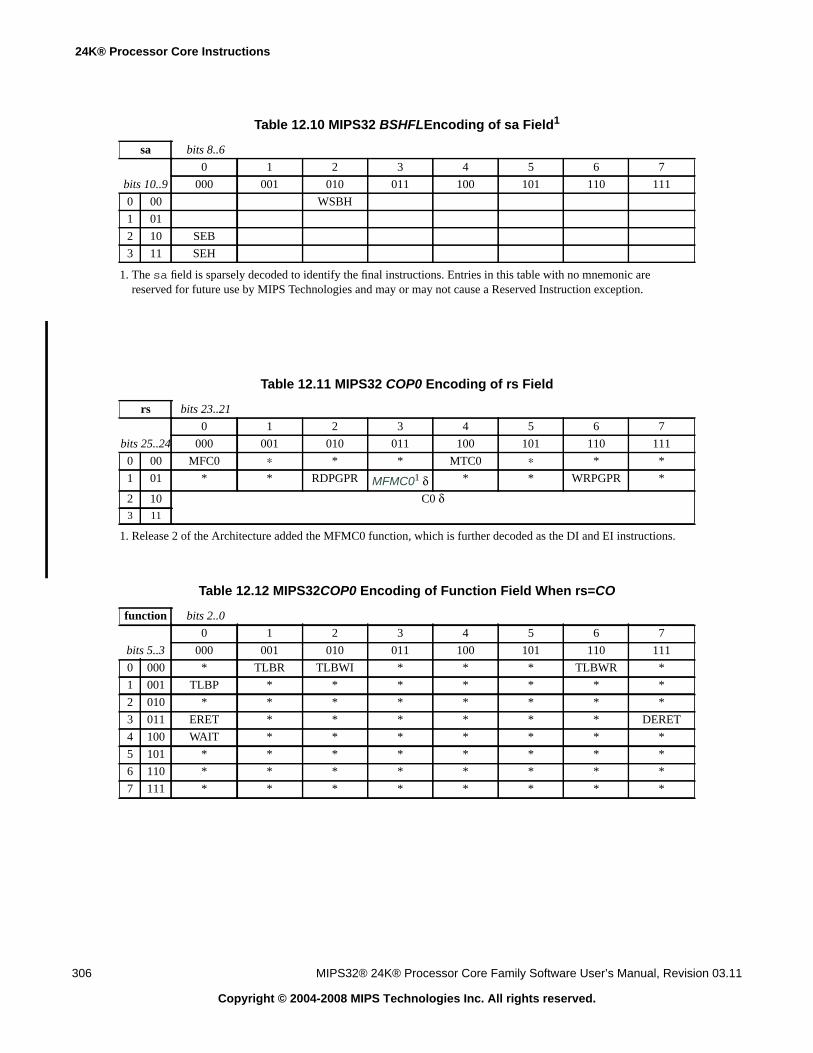
24K® Processor Core Instructions
306 MIPS32® 24K® Processor Core Family Software User’s Manual, Revision 03.11
Copyright © 2004-2008 MIPS Technologies Inc. All rights reserved.
Table 12.10 MIPS32 BSHFLEncoding of sa Field1
1. The sa field is sparsely decoded to identify the final instructions. Entries in this table with no mnemonic arereserved for future use by MIPS Technologies and may or may not cause a Reserved Instruction exception.
sa bits 8..6
0 1 2 3 4 5 6 7
bits 10..9 000 001 010 011 100 101 110 111
0 00 WSBH
1 01
2 10 SEB
3 11 SEH
Table 12.11 MIPS32 COP0 Encoding of rs Field
rs bits 23..21
0 1 2 3 4 5 6 7
bits 25..24 000 001 010 011 100 101 110 111
0 00 MFC0 ∗ * * MTC0 ∗ * *
1 01 * * RDPGPR MFMC01 δ
1. Release 2 of the Architecture added the MFMC0 function, which is further decoded as the DI and EI instructions.
* * WRPGPR *
2 10 C0 δ3 11
Table 12.12 MIPS32COP0 Encoding of Function Field When rs=CO
function bits 2..0
0 1 2 3 4 5 6 7
bits 5..3 000 001 010 011 100 101 110 111
0 000 * TLBR TLBWI * * * TLBWR *
1 001 TLBP * * * * * * *
2 010 * * * * * * * *
3 011 ERET * * * * * * DERET
4 100 WAIT * * * * * * *
5 101 * * * * * * * *
6 110 * * * * * * * *
7 111 * * * * * * * *
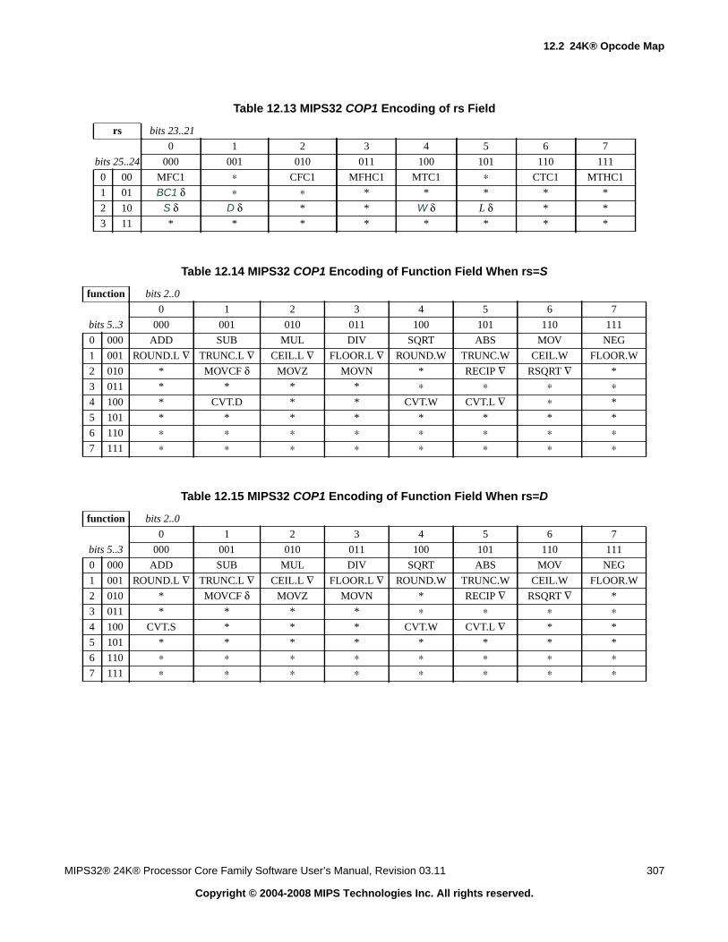
12.2 24K® Opcode Map
MIPS32® 24K® Processor Core Family Software User’s Manual, Revision 03.11 307
Copyright © 2004-2008 MIPS Technologies Inc. All rights reserved.
Table 12.13 MIPS32 COP1 Encoding of rs Field
rs bits 23..21
0 1 2 3 4 5 6 7
bits 25..24 000 001 010 011 100 101 110 111
0 00 MFC1 ∗ CFC1 MFHC1 MTC1 ∗ CTC1 MTHC1
1 01 BC1 δ ∗ ∗ * * * * *
2 10 S δ D δ * * W δ L δ * *
3 11 * * * * * * * *
Table 12.14 MIPS32 COP1 Encoding of Function Field When rs=S
function bits 2..0
0 1 2 3 4 5 6 7
bits 5..3 000 001 010 011 100 101 110 111
0 000 ADD SUB MUL DIV SQRT ABS MOV NEG
1 001 ROUND.L ∇ TRUNC.L ∇ CEIL.L ∇ FLOOR.L ∇ ROUND.W TRUNC.W CEIL.W FLOOR.W
2 010 * MOVCF δ MOVZ MOVN * RECIP ∇ RSQRT ∇ *
3 011 * * * * ∗ ∗ ∗ ∗4 100 * CVT.D * * CVT.W CVT.L ∇ ∗ *
5 101 * * * * * * * *
6 110 ∗ ∗ ∗ ∗ ∗ ∗ ∗ ∗7 111 ∗ ∗ ∗ ∗ ∗ ∗ ∗ ∗
Table 12.15 MIPS32 COP1 Encoding of Function Field When rs=D
function bits 2..0
0 1 2 3 4 5 6 7
bits 5..3 000 001 010 011 100 101 110 111
0 000 ADD SUB MUL DIV SQRT ABS MOV NEG
1 001 ROUND.L ∇ TRUNC.L ∇ CEIL.L ∇ FLOOR.L ∇ ROUND.W TRUNC.W CEIL.W FLOOR.W
2 010 * MOVCF δ MOVZ MOVN * RECIP ∇ RSQRT ∇ *
3 011 * * * * ∗ ∗ ∗ ∗4 100 CVT.S * * * CVT.W CVT.L ∇ * *
5 101 * * * * * * * *
6 110 ∗ ∗ ∗ ∗ ∗ ∗ ∗ ∗7 111 ∗ ∗ ∗ ∗ ∗ ∗ ∗ ∗
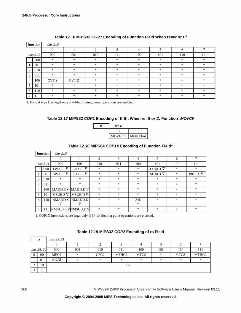
24K® Processor Core Instructions
308 MIPS32® 24K® Processor Core Family Software User’s Manual, Revision 03.11
Copyright © 2004-2008 MIPS Technologies Inc. All rights reserved.
Table 12.16 MIPS32 COP1 Encoding of Function Field When rs=W or L1
1. Format type L is legal only if 64-bit floating point operations are enabled.
function bits 2..0
0 1 2 3 4 5 6 7
bits 5..3 000 001 010 011 100 101 110 111
0 000 * * * * * * * *
1 001 * * * * * * * *
2 010 * * * * * * * *
3 011 * * * * * * * *
4 100 CVT.S CVT.D * * * * ∗ *
5 101 * * * * * * * *
6 110 * * * * * * * *
7 111 * * * * * * * *
Table 12.17 MIPS32 COP1 Encoding of tf Bit When rs=S or D, Function=MOVCF
tf bit 16
0 1
MOVF.fmt MOVT.fmt
Table 12.18 MIPS64 COP1X Encoding of Function Field1
1. COP1X instructions are legal only if 64-bit floating point operations are enabled.
function bits 2..0
0 1 2 3 4 5 6 7
bits 5..3 000 001 010 011 100 101 110 111
0 000 LWXC1 ∇ LDXC1 ∇ * * * LUXC1 ∇ * *
1 001 SWXC1 ∇ SDXC1 ∇ * * * SUXC1 ∇ * PREFX ∇2 010 * * * * * * * *
3 011 * * * * * * ∗ *
4 100 MADD.S ∇ MADD.D ∇ * * * * ∗ *
5 101 MSUB.S ∇ MSUB.D ∇ * * * * ∗ *
6 110 NMADD.S∇
NMADD.D∇
* * 24k*
* ∗ *
7 111 NMSUB.S ∇NMSUB.D ∇ * * * * ∗ *
Table 12.19 MIPS32 COP2 Encoding of rs Field
rs bits 23..21
0 1 2 3 4 5 6 7
bits 25..24 000 001 010 011 100 101 110 111
0 00 MFC2 ∗ CFC2 MFHC2 MTC2 ∗ CTC2 MTHC2
1 01 BC2δ ∗ ∗ * * * * *
2 10 C2
3 11

12.3 Floating Point Unit Instruction Format Encodings
MIPS32® 24K® Processor Core Family Software User’s Manual, Revision 03.11 309
Copyright © 2004-2008 MIPS Technologies Inc. All rights reserved.
12.3 Floating Point Unit Instruction Format Encodings
Instruction format encodings for the floating point unit are presented in this section. This information is a tabular pre-sentation of the encodings described in tables Table 12.13 and Table 12.18 above.
12.4 MIPS32® Instruction Set for the 24K® Core
This section describes the MIPS32 instructions for the 24K cores. Table 12.21 lists the instructions in alphabeticalorder. Instructions that have implementation dependent behavior are described afterwards. The descriptions for otherinstructions exist in the architecture reference manual and are not duplicated here.
Table 12.20 Floating Point Unit Instruction Format Encodings
fmt field(bits 25..21 of COP1
opcode)
fmt3 field(bits 2..0 of COP1X
opcode)
Mnemonic Name Bit Width Data TypeDecimal Hex Decimal Hex
0..15 00..0F — — Used to encode Coprocessor 1 interface instructions (MFC1,CTC1, etc.). Not used for format encoding.
16 10 0 0 S Single 32 Floating Point
17 11 1 1 D Double 64 Floating Point
18..19 12..13 2..3 2..3 Reserved for future use by the architecture.
20 14 4 4 W Word 32 Fixed Point
21 15 5 5 L Long 64 Fixed Point
22 16 6 6 PS Paired Single 2 × 32 Floating Point
23 17 7 7 Reserved for future use by the architecture.
24..31 18..1F — — Reserved for future use by the architecture. Not available forfmt3 encoding.
Table 12.21 24K™ Core Instruction Set
Instruction Description Function
ABS.fmt Floating Point Absolute Valuefmt = s,d
Fd = abs(Fs)
ADD Integer Add Rd = Rs + Rt
ADD.fmt Floating Point Addfmt = s,d
Fd = Fs + Ft
ADDI Integer Add Immediate Rt = Rs + Immed
ADDIU Unsigned Integer Add Immediate Rt = Rs +U Immed
ADDIUPC Unsigned Integer Add Immediate to PC (MIPS16 only) Rt = PC +u Immed
ADDU Unsigned Integer Add Rd = Rs +U Rt
AND Logical AND Rd = Rs & Rt
ANDI Logical AND Immediate Rt = Rs & (016 || Immed)

24K® Processor Core Instructions
310 MIPS32® 24K® Processor Core Family Software User’s Manual, Revision 03.11
Copyright © 2004-2008 MIPS Technologies Inc. All rights reserved.
B Unconditional Branch(Assembler idiom for: BEQ r0, r0, offset)
PC += (int)offset
BAL Branch and Link(Assembler idiom for: BGEZAL r0, offset)
GPR[31] = PC + 8PC += (int)offset
BC1F Branch On Floating Point False if (cc[i] == 0) then PC += (int)offset
BC1FL Branch On Floating Point False Likely if (cc[i] == 0)thenPC += (int)offset
elseIgnore Next Instruction
BC1T Branch On Floating Point True if(cc[i] == 1) thenPC += (int)offset
BC1TL Branch On Floating Point True Likely if (cc[i] == 1) thenPC += (int)offset
elseIgnore Next Instruction
BC2F Branch On CP2 False if (cc[i] == 0) then PC += (int)offset
BC2FL Branch On CP2 False Likely if (cc[i] == 0)thenPC += (int)offset
elseIgnore Next Instruction
BC2T Branch On CP2 True if(cc[i] == 1) thenPC += (int)offset
BC2TL Branch On CP2 True Likely if (cc[i] == 1) thenPC += (int)offset
elseIgnore Next Instruction
BEQ Branch On Equal if Rs == RtPC += (int)offset
BEQL Branch On Equal Likely if Rs == RtPC += (int)offset
elseIgnore Next Instruction
BGEZ Branch on Greater Than or Equal To Zero if !Rs[31]PC += (int)offset
BGEZAL Branch on Greater Than or Equal To Zero And Link GPR[31] = PC + 8if !Rs[31]
PC += (int)offset
BGEZALL Branch on Greater Than or Equal To Zero And LinkLikely
GPR[31] = PC + 8if !Rs[31]
PC += (int)offsetelse
Ignore Next Instruction
Table 12.21 24K™ Core Instruction Set (Continued)
Instruction Description Function
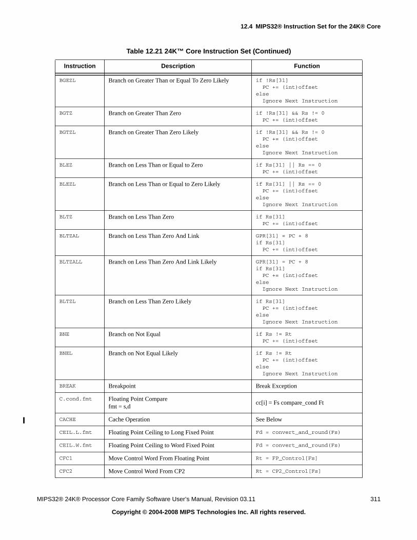
12.4 MIPS32® Instruction Set for the 24K® Core
MIPS32® 24K® Processor Core Family Software User’s Manual, Revision 03.11 311
Copyright © 2004-2008 MIPS Technologies Inc. All rights reserved.
BGEZL Branch on Greater Than or Equal To Zero Likely if !Rs[31]PC += (int)offset
elseIgnore Next Instruction
BGTZ Branch on Greater Than Zero if !Rs[31] && Rs != 0PC += (int)offset
BGTZL Branch on Greater Than Zero Likely if !Rs[31] && Rs != 0PC += (int)offset
elseIgnore Next Instruction
BLEZ Branch on Less Than or Equal to Zero if Rs[31] || Rs == 0PC += (int)offset
BLEZL Branch on Less Than or Equal to Zero Likely if Rs[31] || Rs == 0PC += (int)offset
elseIgnore Next Instruction
BLTZ Branch on Less Than Zero if Rs[31]PC += (int)offset
BLTZAL Branch on Less Than Zero And Link GPR[31] = PC + 8if Rs[31]
PC += (int)offset
BLTZALL Branch on Less Than Zero And Link Likely GPR[31] = PC + 8if Rs[31]
PC += (int)offsetelse
Ignore Next Instruction
BLTZL Branch on Less Than Zero Likely if Rs[31]PC += (int)offset
elseIgnore Next Instruction
BNE Branch on Not Equal if Rs != RtPC += (int)offset
BNEL Branch on Not Equal Likely if Rs != RtPC += (int)offset
elseIgnore Next Instruction
BREAK Breakpoint Break Exception
C.cond.fmt Floating Point Comparefmt = s,d
cc[i] = Fs compare_cond Ft
CACHE Cache Operation See Below
CEIL.L.fmt Floating Point Ceiling to Long Fixed Point Fd = convert_and_round(Fs)
CEIL.W.fmt Floating Point Ceiling to Word Fixed Point Fd = convert_and_round(Fs)
CFC1 Move Control Word From Floating Point Rt = FP_Control[Fs]
CFC2 Move Control Word From CP2 Rt = CP2_Control[Fs]
Table 12.21 24K™ Core Instruction Set (Continued)
Instruction Description Function

24K® Processor Core Instructions
312 MIPS32® 24K® Processor Core Family Software User’s Manual, Revision 03.11
Copyright © 2004-2008 MIPS Technologies Inc. All rights reserved.
CLO Count Leading Ones Rd = NumLeadingOnes(Rs)
CLZ Count Leading Zeroes Rd = NumLeadingZeroes(Rs)
COP2 Coprocessor 2 Operation Implementation dependent
CTC1 Move Control Word To Floating Point FP_Control[Fs] = Rt
CTC2 Move Control Word to CP2 CP2 Control[Fs] = Rt
CVT.D.fmt Floating Point Convert to Double Floating Pointfmt = S,W,L
Fd = convert_and_round(Fs)
CVT.D.fmt Floating Point Convert to Double Floating Pointfmt = S,W,L
Fd = convert_and_round(Fs)
CVT.L.fmt Floating Point Convert to Long Fixed Pointfmt = S,D
Fd = convert_and_round(Fs)
CVT.S.fmt Floating Point Convert to Single Floating Pointfmt = W,D,L
Fd = convert_and_round(Fs)
CVT.W.fmt Floating Point Convert to Word Fixed Pointfmt = S,D
Fd = convert_and_round(Fs)
DERET Return from Debug Exception PC = DEPCExit Debug Mode
DI Atomically Disable Interrupts Rt = Status; StatusIE = 0
DIV Divide LO = (int)Rs / (int)RtHI = (int)Rs % (int)Rt
DIV.fmt Floating Point Dividefmt = S,D
Fd = Fs/Ft
DIVU Unsigned Divide LO = (uns)Rs / (uns)RtHI = (uns)Rs % (uns)Rt
EHB Execution Hazard Barrier Stop instruction execution until executionhazards are cleared
EI Atomically Enable Interrupts Rt = Status; StatusIE = 1
ERET Return from Exception if SR[2]PC = ErrorEPC
elsePC = EPCSR[1] = 0
SR[2] = 0LL = 0
EXT Extract Bit Field Rt = ExtractField(Rs, pos, size)
FLOOR.L.fmt Floating Point Floor to Long Fixed Pointfmt = S,D
Fd = convert_and_round(Fs)
FLOOR.W.fmt Floating Point Floor to Word Fixed Pointfmt = S,D
Fd = convert_and_round(Fs)
Table 12.21 24K™ Core Instruction Set (Continued)
Instruction Description Function

12.4 MIPS32® Instruction Set for the 24K® Core
MIPS32® 24K® Processor Core Family Software User’s Manual, Revision 03.11 313
Copyright © 2004-2008 MIPS Technologies Inc. All rights reserved.
INS Insert Bit Field Rt = InsertField(Rs, Rt, pos,size)
J Unconditional Jump PC = PC[31:28] || offset<<2
JAL Jump and Link GPR[31] = PC + 8PC = PC[31:28] || offset<<2
JALR Jump and Link Register Rd = PC + 8PC = Rs
JALR.HB Jump and Link Register with Hazard Barrier Like JALR, but also clears execution andinstruction hazards
JALRC Jump and Link Register Compact - do not executeinstruction in jump delay slot(MIPS16 only)
Rd = PC + 2PC = Rs
JR Jump Register PC = Rs
JR.HB Jump Register with Hazard Barrier Like JR, but also clears execution andinstruction hazards
JRC Jump Register Compact - do not execute instruction injump delay slot (MIPS16 only)
PC = Rs
LB Load Byte Rt = (byte)Mem[base+offset]
LBU Unsigned Load Byte Rt = (ubyte)Mem[base+offset]
LDC1 Load Doubleword to Floating Point Ft = memory[base+offset]
LDC2 Load Doubleword to CP2 Ft = memory[base+offset]
LDXC1 Load Doubleword Indexed to Floating Point Fd = memory[base+index]
LH Load Halfword Rt = (half)Mem[base+offset]
LHU Unsigned Load Halfword Rt = (uhalf)Mem[base+offset]
LL Load Linked Word Rt = Mem[base+offset]LL = 1
LUI Load Upper Immediate Rt = immediate << 16
LUXC1 Load Doubleword Indexed Unaligned to Floating Point Fd =memory[(base+index)psize-1..3
LW Load Word Rt = Mem[Rs+offset]
LWC1 Load Word to Floating Point Ft = memory[base+offset]
LWC2 Load Word to CP2 Ft = memory[base+offset]
LWPC Load Word, PC relative Rt = Mem[PC+offset]
LWXC1 Load Word Indexed to Floating Point Fd = memory[base+index]
LWL Load Word Left See Architecture Reference Manual
LWR Load Word Right See Architecture Reference Manual
MADD Multiply-Add HI | LO += (int)Rs * (int)Rt
Table 12.21 24K™ Core Instruction Set (Continued)
Instruction Description Function

24K® Processor Core Instructions
314 MIPS32® 24K® Processor Core Family Software User’s Manual, Revision 03.11
Copyright © 2004-2008 MIPS Technologies Inc. All rights reserved.
MADD.fmt Floating Point Multiply Addfmt = S,D
Fd = Fs * Ft + Fr
MADDU Multiply-Add Unsigned HI | LO += (uns)Rs * (uns)Rt
MFC0 Move From Coprocessor 0 Rt = CPR[0, Rd, sel]
MFC1 Move From FPR Rt = Fs31..0
MFC2 Move From CP2 Register Rt = Fs31..0
MFHC1 Move From High Half of FPR Rt = Fs63..32
MFHC2 Move From High Half of CP2 Register Rt = Fs63..32
MFHI Move From HI Rd = HI
MFLO Move From LO Rd = LO
MOV.fmt Floating Point Move Fd = Fs
MOVF GPR Conditional Move on Floating Point False if (cc[i] == 0) then Rd = Rs
MOVF.fmt FPR Conditional Move on Floating Point False if (cc[i] == 0) then Fd = Fs
MOVN GPR Conditional Move on Not Zero if Rt ≠ 0 thenRd = Rs
MOVN.fmt FPR Conditional Move on Not Zero if Rt ≠ 0 thenFd = Fs
MOVT GPR Conditional Move on Floating Point True if (cc[i] == 1) then Rd = Rs
MOVT.fmt FPR Conditional Move on Floating Point True if (cc[i] == 1) then Fd = Fs
MOVZ GPR Conditional Move on Zero if Rt = 0 thenRd = Rs
MOVZ.fmt FPR Conditional Move on Zero if (Rt == 0) then Fd = Fs
MSUB Multiply-Subtract HI | LO -= (int)Rs * (int)Rt
MSUB.fmt Floating Point Multiply Subtractfmt = S,D
Fd = Fs * Ft - Fr
MSUBU Multiply-Subtract Unsigned HI | LO -= (uns)Rs * (uns)Rt
MTC0 Move To Coprocessor 0 CPR[0, n, Sel] = Rt
MTC1 Move To FPR Fs = Rt
MTC2 Move to CP2 register Fs = Rt
MTHC1 Move To High Half of FPR Fd = Rt || Fs31..0
MTHC2 Move to High Half of CP2 register Fd = Rt || Fs31..0
MTHI Move To HI HI = Rs
MTLO Move To LO LO = Rs
Table 12.21 24K™ Core Instruction Set (Continued)
Instruction Description Function
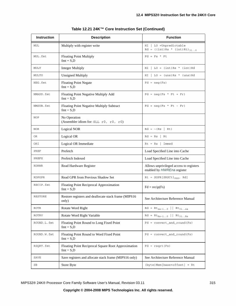
12.4 MIPS32® Instruction Set for the 24K® Core
MIPS32® 24K® Processor Core Family Software User’s Manual, Revision 03.11 315
Copyright © 2004-2008 MIPS Technologies Inc. All rights reserved.
MUL Multiply with register write HI | LO =UnpredictableRd = ((int)Rs * (int)Rt)31..0
MUL.fmt Floating Point Multiplyfmt = S,D
Fd = Fs * Ft
MULT Integer Multiply HI | LO = (int)Rs * (int)Rd
MULTU Unsigned Multiply HI | LO = (uns)Rs * (uns)Rd
NEG.fmt Floating Point Negatefmt = S,D
Fd = neg(Fs)
NMADD.fmt Floating Point Negative Multiply Addfmt = S,D
Fd = neg(Fs * Ft + Fr)
NMSUB.fmt Floating Point Negative Multiply Subtractfmt = S,D
Fd = neg(Fs * Ft - Fr)
NOP No Operation(Assembler idiom for: SLL r0, r0, r0)
NOR Logical NOR Rd = ~(Rs | Rt)
OR Logical OR Rd = Rs | Rt
ORI Logical OR Immediate Rt = Rs | Immed
PREF Prefetch Load Specified Line into Cache
PREFX Prefetch Indexed Load Specified Line into Cache
RDHWR Read Hardware Register Allows unprivileged access to registersenabled by HWREna register
RDPGPR Read GPR from Previous Shadow Set Rt = SGPR[SRSCtlPSS, Rd]
RECIP.fmt Floating Point Reciprocal Approximationfmt = S,D
Fd = recip(Fs)
RESTORE Restore registers and deallocate stack frame (MIPS16only)
See Architecture Reference Manual
ROTR Rotate Word Right Rd = Rtsa-1..0 || Rt31..sa
ROTRV Rotate Word Right Variable Rd = RtRs-1..0 || Rt31..Rs
ROUND.L.fmt Floating Point Round to Long Fixed Pointfmt = S,D
Fd = convert_and_round(Fs)
ROUND.W.fmt Floating Point Round to Word Fixed Pointfmt = S,D
Fd = convert_and_round(Fs)
RSQRT.fmt Floating Point Reciprocal Square Root Approximationfmt = S,D
Fd = rsqrt(Fs)
SAVE Save registers and allocate stack frame (MIPS16 only) See Architecture Reference Manual
SB Store Byte (byte)Mem[base+offset] = Rt
Table 12.21 24K™ Core Instruction Set (Continued)
Instruction Description Function

24K® Processor Core Instructions
316 MIPS32® 24K® Processor Core Family Software User’s Manual, Revision 03.11
Copyright © 2004-2008 MIPS Technologies Inc. All rights reserved.
SC Store Conditional Word if LL = 1 mem[base+offset] = RtRt = LL
SDBBP Software Debug Break Point Trap to SW Debug Handler
SDC1 Store Doubleword from Floating Point memory[base+offset] = Ft
SDC2 Store Doubleword from CP2 memory[base+offset] = Ft
SDXC1 Store Word Indexed from Floating Point memory[base+index] = Fs
SEB Sign Extend Byte Rd = (byte)Rs
SEH Sign Extend Half Rd = (half)Rs
SH Store Half (half)Mem[base+offset] = Rt
SLL Shift Left Logical Rd = Rt << sa
SLLV Shift Left Logical Variable Rd = Rt << Rs[4:0]
SLT Set on Less Than if (int)Rs < (int)RtRd = 1
elseRd = 0
SLTI Set on Less Than Immediate if (int)Rs < (int)ImmedRt = 1
elseRt = 0
SLTIU Set on Less Than Immediate Unsigned if (uns)Rs < (uns)ImmedRt = 1
elseRt = 0
SLTU Set on Less Than Unsigned if (uns)Rs < (uns)ImmedRd = 1
elseRd = 0
SQRT.fmt Floating Point Square Rootfmt = S,D
Fd = sqrt(Fs)
SRA Shift Right Arithmetic Rd = (int)Rt >> sa
SRAV Shift Right Arithmetic Variable Rd = (int)Rt >> Rs[4:0]
SRL Shift Right Logical Rd = (uns)Rt >> sa
SRLV Shift Right Logical Variable Rd = (uns)Rt >> Rs[4:0]
SSNOP Superscalar Inhibit No Operation NOP
SUB Integer Subtract Rt = (int)Rs - (int)Rd
SUB.fmt Floating Point Subtractfmt = S,D
Fd = Fs - Ft
SUBU Unsigned Subtract Rt = (uns)Rs - (uns)Rd
Table 12.21 24K™ Core Instruction Set (Continued)
Instruction Description Function

12.4 MIPS32® Instruction Set for the 24K® Core
MIPS32® 24K® Processor Core Family Software User’s Manual, Revision 03.11 317
Copyright © 2004-2008 MIPS Technologies Inc. All rights reserved.
SUXC1 Store Doubleword Indexed Unaligned from FloatingPoint
memory[(base+index)psize-1..3]= Fs
SW Store Word Mem[base+offset] = Rt
SWC1 Store Word From Floating Point Mem[base+offset] = Fs
SWC2 Store Word From CP2 Register Mem[base+offset] = Fs
SWL Store Word Left See Architecture Reference Manual
SWR Store Word Right See Architecture Reference Manual
SWXC1 Store Word Indexed to Floating Point memory[base+index] = Fs
SYNC Synchronize See Below
SYNCI Synchronize Caches to Make Instruction Writes Effec-tive
For D-cache writeback and I-cacheinvalidate on specified address
SYSCALL System Call SystemCallException
TEQ Trap if Equal if Rs == RtTrapException
TEQI Trap if Equal Immediate if Rs == (int)Immed TrapException
TGE Trap if Greater Than or Equal if (int)Rs >= (int)Rt TrapException
TGEI Trap if Greater Than or Equal Immediate if (int)Rs >= (int)Immed TrapException
TGEIU Trap if Greater Than or Equal Immediate Unsigned if (uns)Rs >= (uns)Immed TrapException
TGEU Trap if Greater Than or Equal Unsigned if (uns)Rs >= (uns)Rt TrapException
TLBWI Write Indexed TLB Entry See Below
TLBWR Write Random TLB Entry See Below
TLBP Probe TLB for Matching Entry See Architecture Reference Manual
TLBR Read Index for TLB Entry See Below
TLT Trap if Less Than if (int)Rs < (int)Rt TrapException
TLTI Trap if Less Than Immediate if (int)Rs < (int)Immed TrapException
TLTIU Trap if Less Than Immediate Unsigned if (uns)Rs < (uns)Immed TrapException
TLTU Trap if Less Than Unsigned if (uns)Rs < (uns)Rt TrapException
TNE Trap if Not Equal if Rs != Rt TrapException
Table 12.21 24K™ Core Instruction Set (Continued)
Instruction Description Function

24K® Processor Core Instructions
318 MIPS32® 24K® Processor Core Family Software User’s Manual, Revision 03.11
Copyright © 2004-2008 MIPS Technologies Inc. All rights reserved.
.
TNEI Trap if Not Equal Immediate if Rs != (int)Immed TrapException
TRUNC.L.fmt Floating Point Truncate to Long Fixed Point Fd = convert_and_round(Fs)
TRUNC.W.fmt Floating Point Truncate to Word Fixed Point Fd = convert_and_round(Fs)
WAIT Wait for Interrupts Stall until interrupt occurs
WRPGPR Write to GPR in Previous Shadow Set SGPR[SRSCtlPSS, Rd] = Rt
WSBH Word Swap Bytes Within HalfWords Rd = Rt23..16 || Rt31..24 || Rt7..0|| Rt15..8
XOR Exclusive OR Rd = Rs ^ Rt
XORI Exclusive OR Immediate Rt = Rs ^ (uns)Immed
ZEB Zero extend byte (MIPS16 only) Rt = (ubyte) Rs
ZEH Zero extend half (MIPS16 only) Rt = (uhalf) Rs
Table 12.22 List of instructions in the MIPS32® DSP ASE in the Arithmetic sub-class
InstructionMnemonics
InputDataType
OutputDataType
WritesGPR / ac /
DSPControl App Description
ADDQ.PH rd,rs,rtADDQ_S.PH rd,rs,rt
Pair Q15 Pair Q15 GPR VoIPSoftM
Element-wise addition of two vectors of Q15fractional values, with optional saturation.
ADDQ_S.W rd,rs,rt Q31 Q31 GPR Audio Add two Q31 fractional values with saturation.
ADDU.QB rd,rs,rtADDU_S.QB rd,rs,rt
QuadUnsignedByte
QuadUnsignedByte
GPR Video Element-wise addition of vectors of fourunsigned byte values. Results may be option-ally saturated to 255.
SUBQ.PH rd,rs,rtSUBQ_S.PH rd,rs,rt
Pair Q15 Pair Q15 GPR VoIP Element-wise subtraction of two vectors ofQ15 fractional values, with optional satura-tion.
SUBQ_S.W rd,rs,rt Q31 Q31 GPR Audio Subtraction with Q31 fractional values, withsaturation.
SUBU.QB rd,rs,rtSUBU_S.QB rd,rs,rt
QuadUnsignedByte
QuadUnsignedByte
GPR Video Element-wise subtraction of unsigned bytevalues, with optional unsigned saturation.
ADDSC rd,rs,rt SignedWord
SignedWord
GPR &DSPControl
Audio Add two signed words and set the carry bit inthe DSPControl register.
ADDWC rd,rs,rt SignedWord
SignedWord
GPR Audio Add two signed words with the carry bit fromthe DSPControl register.
Table 12.21 24K™ Core Instruction Set (Continued)
Instruction Description Function

12.4 MIPS32® Instruction Set for the 24K® Core
MIPS32® 24K® Processor Core Family Software User’s Manual, Revision 03.11 319
Copyright © 2004-2008 MIPS Technologies Inc. All rights reserved.
MODSUB rd,rs,rt SignedWord
SignedWord
GPR Misc Modulo addressing support: update a byteindex into a circular buffer by subtracting aspecified decrement (in bytes) from the index,resetting the index to a specified value if thesubtraction results in underflow.
RADDU.W.QB rd,rs QuadUnsignedByte
UnsignedWord
GPR Misc Reduce (add together) the 4 unsigned byte val-ues in rs, zero-extending the sum to 32 bitsbefore writing to the destination register. Forexample, if all 4 input values are 0x80 (deci-mal 128), then the result in rd is 0x200 (deci-mal 512).
ABSQ_S.PH rd,rt Pair Q15 Pair Q15 GPR Misc Find the absolute value of each of two Q15fractional halfword elements in the source reg-ister, saturating values of -1.0 to the maximumpositive Q15 fractional value.
ABSQ_S.W rd,rt Q31 Q31 GPR Misc Find the absolute value of the Q31 fractionalelement in the source register, saturating thevalue -1.0 to the maximum positive Q31 frac-tional value.
PRECRQ.QB.PH rd,rs,rt 2 Pair Q15 Quad Byte GPR Misc Reduce the precision of four Q15 fractionalinput values by truncation to create four Q7fractional output values. The two Q15 valuesfrom register rs are written to the twoleft-most byte results, allowing anendian-agnostic implementation.
PRECR_SRA.PH.Wrt,rs,saPRECR_SRA_R.PH.Wrt,rs,sa
Two Inte-ger Words
Pair IntegerHalfword
GPR Misc Reduce the precision of two integer word val-ues to create a pair of integer halfword values.Each word value is first shifted right arithmeti-cally by sa bit positions, and optionallyrounded up by adding 1 at the most-significantdiscard bit position. The 16 least-significantbits of each word are then written to the corre-sponding halfword elements of destinationregister rt.
PRECRQ.PH.W rd,rs,rtPRECRQ_RS.PH.Wrd,rs,rt
2 Q31 Pair half-word
GPR Misc Reduce the precision of two Q31 fractionalinput values by truncation to create two Q15fractional output values. The Q15 valueobtained from register rs creates the left-mostresult, allowing an endian-agnostic implemen-tation. Results may be optionally rounded upand saturated before being written to the desti-nation.
PRECRQU_S.QB.PHrd,rs,rt
2 Pair Q15 QuadUnsignedByte
GPR Misc Reduce the precision of four Q15 fractionalvalues by saturating and truncating to createfour unsigned byte values.
Table 12.22 List of instructions in the MIPS32® DSP ASE in the Arithmetic sub-class (Continued)
InstructionMnemonics
InputDataType
OutputDataType
WritesGPR / ac /
DSPControl App Description

24K® Processor Core Instructions
320 MIPS32® 24K® Processor Core Family Software User’s Manual, Revision 03.11
Copyright © 2004-2008 MIPS Technologies Inc. All rights reserved.
PRECEQ.W.PHL rd,rtPRECEQ.W.PHR rd,rt
Q15 Q31 GPR Misc Expand the precision of a Q15 fractional valueto create a Q31 fractional value by adding 16least-significant bits to the input value.
PRECEQU.PH.QBL rd,rtPRECEQU.PH.QBR rd,rtPRECEQU.PH.QBLArd,rtPRECEQU.PH.QBRArd,rt
UnsignedByte
Q15 GPR Video Expand the precision of two unsigned bytevalues by prepending a sign bit and addingseven least-significant bits to each to createtwo Q15 fractional values.
PRECEU.PH.QBL rd,rtPRECEU.PH.QBR rd,rtPRECEU.PH.QBLA rd,rtPRECEU.PH.QBRA rd,rt
UnsignedByte
Unsignedhalfword
GPR Video Expand the precision of two unsigned bytevalues by adding eight least-significant bits toeach to create two unsigned halfword values.
Table 12.23 List of instructions in the MIPS32® DSP ASE in the GPR-Based Shift sub-class
InstructionMnemonics
InputDataType
OutputDataType
WritesGPR / ac /
DSPControl App Description
SHLL.QB rd, rt, saSHLLV.QB rd, rt, rs
QuadUnsignedByte
QuadUnsignedByte
GPR Misc Element-wise left shift of eight signed bytes.Zeros are inserted into the bits emptied by theshift. The shift amount is specified by the threeleast-significant bits of sa or rs.
SHLL.PH rd, rt, saSHLLV.PH rd, rt, rsSHLL_S.PH rd, rt, saSHLLV_S.PH rd, rt, rs
Pair Signedhalfword
Pair Signedhalfword
GPR Misc Element-wise left shift of two signed half-words, with optional saturation on overflow.Zeros are inserted into the bits emptied by theshift. The shift amount is specified by the fourleast-significant bits of sa or rs.
SHLL_S.W rd, rt, saSHLLV_S.W rd, rt, rs
SignedWord
SignedWord
GPR Misc Left shift of a signed word, with saturation onoverflow. Zeros are inserted into the bits emp-tied by the shift. The shift amount is specifiedby the five least-significant bits of sa or rs.Use the MIPS32 instructions SLL or SLLV fornon-saturating shift operations.
SHRL.QB rd, rt, saSHRLV.QB rd, rt, rs
QuadUnsignedByte
QuadUnsignedByte
GPR Video Element-wise logical right shift of four bytevalues. Zeros are inserted into the bits emptiedby the shift. The shift amount is specified bythe three least-significant bits of sa or rs.
SHRA.PH rd, rt, saSHRAV.PH rd, rt, rsSHRA_R.PH rd, rt, saSHRAV_R.PH rd, rt, rs
Pair Signedhalfword
Pair Signedhalfword
GPR Misc Element-wise arithmetic (sign preserving)right shift of two halfword values. Optionally,rounding may be performed, adding 1 at themost-significant discard bit position. The shiftamount is specified by the four least-signifi-cant bits of rs or by the argument sa.
Table 12.22 List of instructions in the MIPS32® DSP ASE in the Arithmetic sub-class (Continued)
InstructionMnemonics
InputDataType
OutputDataType
WritesGPR / ac /
DSPControl App Description

12.4 MIPS32® Instruction Set for the 24K® Core
MIPS32® 24K® Processor Core Family Software User’s Manual, Revision 03.11 321
Copyright © 2004-2008 MIPS Technologies Inc. All rights reserved.
SHRA_R.W rd, rt, saSHRAV_R.W rd, rt, rs
SignedWord
SignedWord
GPR Video Arithmetic (sign preserving) right shift of aword value. Optionally, rounding may be per-formed, adding 1 at the most-significant dis-card bit position. The shift amount is specifiedby the five least-significant bits of rs or theargument sa.
Table 12.24 List of instructions in the MIPS32® DSP ASE in the Multiply sub-class
InstructionMnemonics
InputDataType
OutputDataType
WritesGPR / ac /
DSPControl App Description
MULEU_S.PH.QBLrd,rs,rtMULEU_S.PH.QBRrd,rs,rt
PairUnsignedByte, PairUnsignedHalfword,
PairUnsignedHalfword
GPR StillImage
Element-wise multiplication of two unsignedbyte values from register rs with two unsignedhalfword values from register rt. Each 24-bitproduct is truncated to 16 bits, with saturationif the product exceeds 0xFFFF, and written tothe corresponding element in the destinationregister.
MULQ_RS.PH rd,rs,rt Pair Q15 Pair Q15 GPR Misc Element-wise multiplication of two Q15 frac-tional values to create two Q15 fractionalresults, with rounding and saturation. Aftermultiplication, each 32-bit product is roundedup by adding 0x00008000, then truncated tocreate a Q15 fractional value that is written tothe destination register. If both multiplicandsare -1.0, the result is saturated to the maximumpositive Q15 fractional value.To stay compliant with the base architecture,this instruction leaves the base HI-LO pairUNPREDICTABLE after the operation. Theother DSP ASE accumulators ac1-ac3 areuntouched.
MULEQ_S.W.PHLrd,rs,rtMULEQ_S.W.PHRrd,rs,rt
Pair Q15 Q31 GPR VoIP Multiplication of two Q15 fractional values,shifting the product left by 1 bit to create aQ31 fractional result. If both multiplicands are-1.0 the result is saturated to the maximumpositive Q31 value.To stay compliant with the base architecture,this instruction leaves the base HI-LO pairUNPREDICTABLE after the operation. Theother DSP ASE accumulators ac1-ac3 mustbe untouched.
Table 12.23 List of instructions in the MIPS32® DSP ASE in the GPR-Based Shift sub-class (Continued)
InstructionMnemonics
InputDataType
OutputDataType
WritesGPR / ac /
DSPControl App Description

24K® Processor Core Instructions
322 MIPS32® 24K® Processor Core Family Software User’s Manual, Revision 03.11
Copyright © 2004-2008 MIPS Technologies Inc. All rights reserved.
DPAU.H.QBLDPAU.H.QBR
Pair Bytes Halfword Acc Image Dot-product accumulation. Two pairs of corre-sponding unsigned byte elements from sourceregisters rt and rs are separately multiplied,and the two 16-bit products are then summedtogether. The summed products are then addedto the accumulator.
DPSU.H.QBLDPSU.H.QBR
Pair Bytes Halfword Acc Image Dot-product subtraction. Two pairs of corre-sponding unsigned byte elements from sourceregisters rt and rs are separately multiplied,and the two 16-bit products are then summedtogether. The summed products are then sub-tracted from the accumulator.
DPAQ_S.W.PH ac,rs,rt Pair Q15 Q32.31 ac VoIP /SoftM
Dot-product accumulation. Two pairs of corre-sponding Q15 fractional values from sourceregisters rt and rs are separately multipliedand left-shifted 1 bit to create two Q31 frac-tional products. For each product, if both mul-tiplicands are equal to -1.0 the product isclamped to the maximum positive Q31 frac-tional value.The products are then summed, and the sum isthen sign extended to the width of the accumu-lator and accumulated into the specified accu-mulator.This instruction may be used to compute theimaginary component of a 16-bit complexmultiplication operation after first swappingthe operands to place them in the correct order.
DPSQ_S.W.PH ac,rs,rt Pair Q15 Q32.31 ac VoIP /SoftM
Dot-product subtraction. Two pairs of corre-sponding Q15 fractional values from sourceregisters rt and rs are separately multipliedand left-shifted 1 bit to create two Q31 frac-tional products. For each product, if both mul-tiplicands are equal to -1.0 the product isclamped to the maximum positive Q31 frac-tional value.The products are then summed, and the sum isthen sign extended to the width of the accumu-lator and subtracted from the specified accu-mulator.This instruction may be used to compute theimaginary component of a 16-bit complexmultiplication operation after first swappingthe operands to place them in the correct order.
Table 12.24 List of instructions in the MIPS32® DSP ASE in the Multiply sub-class (Continued)
InstructionMnemonics
InputDataType
OutputDataType
WritesGPR / ac /
DSPControl App Description
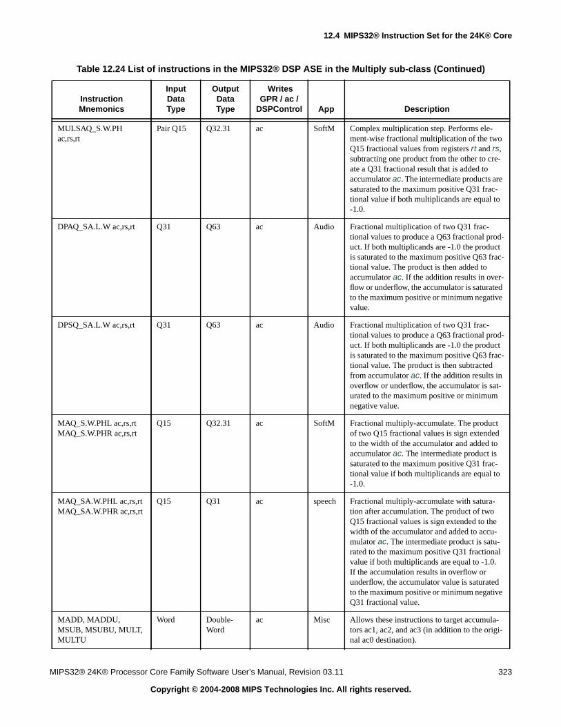
12.4 MIPS32® Instruction Set for the 24K® Core
MIPS32® 24K® Processor Core Family Software User’s Manual, Revision 03.11 323
Copyright © 2004-2008 MIPS Technologies Inc. All rights reserved.
MULSAQ_S.W.PHac,rs,rt
Pair Q15 Q32.31 ac SoftM Complex multiplication step. Performs ele-ment-wise fractional multiplication of the twoQ15 fractional values from registers rt and rs,subtracting one product from the other to cre-ate a Q31 fractional result that is added toaccumulator ac. The intermediate products aresaturated to the maximum positive Q31 frac-tional value if both multiplicands are equal to-1.0.
DPAQ_SA.L.W ac,rs,rt Q31 Q63 ac Audio Fractional multiplication of two Q31 frac-tional values to produce a Q63 fractional prod-uct. If both multiplicands are -1.0 the productis saturated to the maximum positive Q63 frac-tional value. The product is then added toaccumulator ac. If the addition results in over-flow or underflow, the accumulator is saturatedto the maximum positive or minimum negativevalue.
DPSQ_SA.L.W ac,rs,rt Q31 Q63 ac Audio Fractional multiplication of two Q31 frac-tional values to produce a Q63 fractional prod-uct. If both multiplicands are -1.0 the productis saturated to the maximum positive Q63 frac-tional value. The product is then subtractedfrom accumulator ac. If the addition results inoverflow or underflow, the accumulator is sat-urated to the maximum positive or minimumnegative value.
MAQ_S.W.PHL ac,rs,rtMAQ_S.W.PHR ac,rs,rt
Q15 Q32.31 ac SoftM Fractional multiply-accumulate. The productof two Q15 fractional values is sign extendedto the width of the accumulator and added toaccumulator ac. The intermediate product issaturated to the maximum positive Q31 frac-tional value if both multiplicands are equal to-1.0.
MAQ_SA.W.PHL ac,rs,rtMAQ_SA.W.PHR ac,rs,rt
Q15 Q31 ac speech Fractional multiply-accumulate with satura-tion after accumulation. The product of twoQ15 fractional values is sign extended to thewidth of the accumulator and added to accu-mulator ac. The intermediate product is satu-rated to the maximum positive Q31 fractionalvalue if both multiplicands are equal to -1.0.If the accumulation results in overflow orunderflow, the accumulator value is saturatedto the maximum positive or minimum negativeQ31 fractional value.
MADD, MADDU,MSUB, MSUBU, MULT,MULTU
Word Double-Word
ac Misc Allows these instructions to target accumula-tors ac1, ac2, and ac3 (in addition to the origi-nal ac0 destination).
Table 12.24 List of instructions in the MIPS32® DSP ASE in the Multiply sub-class (Continued)
InstructionMnemonics
InputDataType
OutputDataType
WritesGPR / ac /
DSPControl App Description

24K® Processor Core Instructions
324 MIPS32® 24K® Processor Core Family Software User’s Manual, Revision 03.11
Copyright © 2004-2008 MIPS Technologies Inc. All rights reserved.
Table 12.25 List of instructions in the MIPS32® DSP ASE in the Bit/ Manipulation sub-class
InstructionMnemonics
InputDataType
OutputDataType
WritesGPR / ac /
DSPControl App Description
BITREV rd,rt UnsignedWord
UnsignedWord
GPR Audio /FFT
Reverse the order of the 16 least-significantbits of register rt, writing the result to registerrd. The 16 most-significant bits are set to zero.
INSV rt,rs UnsignedWord
UnsignedWord
GPR Misc Like the Release 2 INS instruction, except thatthe 5 bits for pos and size values are obtainedfrom the DSPControl register. size =scount[14:10], and pos = pos[20:16].
REPL.QB rd,immREPLV.QB rd,rt
Byte Quad Byte GPR Video /Misc
Replicate a signed byte value into the four byteelements of register rd. The byte value is givenby the 8 least-significant bits of the specified10-bit immediate constant or by the 8least-significant bits of register rt.
REPL.PH rd,immREPLV.PH rd,rt
Signedhalfword
Pair Signedhalfword
GPR Misc Replicate a signed halfword value into the twohalfword elements of register rd. The halfwordvalue is given by the 16 least-significant bits ofregister rt, or by the value of the 10-bit imme-diate constant, sign-extended to 16 bits.
Table 12.26 List of instructions in the MIPS32® DSP ASE in the Compare-Pick sub-class
InstructionMnemonics
InputDataType
OutputDataType
WritesGPR / ac /
DSPControl App Description
CMPU.EQ.QB rs,rtCMPU.LT.QB rs,rtCMPU.LE.QB rs,rt
QuadUnsignedByte
QuadUnsignedByte
DSPControl Video Element-wise unsigned comparison of the fourunsigned byte elements of rs and rt, recordingthe boolean comparison results to the fourright-most bits in the ccond field of theDSPControl register.
CMPGU.EQ.QB rd,rs,rtCMPGU.LT.QB rd,rs,rtCMPGU.LE.QB rd,rs,rt
QuadUnsignedByte
QuadUnsignedByte
GPR Video Element-wise unsigned comparison of the fourright-most unsigned byte elements of rs and rt,recording the boolean comparison results tothe four least-significant bits of register rd.
CMP.EQ.PH rs,rtCMP.LT.PH rs,rtCMP.LE.PH rs,rt
Pair Signedhalfword
Pair Signedhalfword
DSPControl Misc Element-wise signed comparison of the twohalfword elements of rs and rt, recording theboolean comparison results to the tworight-most bits in the ccond field of theDSPControl register.

12.4 MIPS32® Instruction Set for the 24K® Core
MIPS32® 24K® Processor Core Family Software User’s Manual, Revision 03.11 325
Copyright © 2004-2008 MIPS Technologies Inc. All rights reserved.
PICK.QB rd,rs,rt QuadUnsignedByte
QuadUnsignedByte
GPR Video Element-wise selection of unsigned bytesfrom the four bytes of registers rs and rt intothe corresponding elements of register rd,based on the value of the four right-most bitsof the ccond field in the DSPControl register.If the corresponding ccond bit is 1, the bytevalue is copied from register rs, otherwise it iscopied from rt.
PICK.PH rd,rs,rt Pair Signedhalfword
Pair Signedhalfword
GPR Misc Element-wise selection of signed halfwordsfrom the two halfwords in registers rs and rtinto the corresponding elements of register rd,based on the value of the two right-most bits ofthe ccond field in the DSPControl register. Ifthe corresponding ccond bit is 1, the halfwordvalue is copied from register rs, otherwise it iscopied from rt.
PACKRL.PH rd,rs,rt Pair SignedHalfwords
Pair SignedHalfword
GPR Misc Pack two halfwords taken from registers rsand rt into destination register rd.
Table 12.27 List of instructions in the MIPS32® DSP ASE in the Accumulator and DSPControl Accesssub-class
InstructionMnemonics
InputDataType
OutputDataType
WritesGPR / ac /
DSPControl App Description
EXTR.W rt,ac,shiftEXTR_R.W rt,ac,shiftEXTR_RS.W rt,ac,shift
Q63 Q31 GPR Misc Extract a Q31 fractional value from the 32least-significant bits of 64-bit accumulator ac.The accumulator value may be shifted rightlogically by shift bits prior to the extraction,and the extracted value may be optionallyrounded or rounded and saturated before beingwritten to register rt.The shift argument value ranges from 0 to 31.The optional rounding step adds 1 at themost-significant bit position discarded by theshift. The optional saturation clamps theextracted value to the maximum positive Q31value if the rounding step results in overflow.
Table 12.26 List of instructions in the MIPS32® DSP ASE in the Compare-Pick sub-class (Continued)
InstructionMnemonics
InputDataType
OutputDataType
WritesGPR / ac /
DSPControl App Description

24K® Processor Core Instructions
326 MIPS32® 24K® Processor Core Family Software User’s Manual, Revision 03.11
Copyright © 2004-2008 MIPS Technologies Inc. All rights reserved.
EXTR_S.H rt,ac,shift Q63 Q15 GPR Misc Extract a Q15 fractional value from the 16least-significant bits of 64-bit accumulator ac.The accumulator value may be shifted rightlogically by shift bits prior to the extraction,and the extracted value is saturated beforebeing written to register rt.The shift argument value ranges from 0 to 31.The saturation clamps the extracted value tothe maximum positive or minimum negativeQ15 value if the shifted accumulator valuecannot be represented accurately as a Q15 for-mat value.
EXTRV_S.H rt,ac,rs Q63 Q15 GPR Misc Extract a Q15 fractional value from the 16least-significant bits of 64-bit accumulator ac.The accumulator value may be shifted rightlogically by shift bits prior to the extraction,and the extracted value is saturated beforebeing written to register rt.The shift argument ranges from 0 to 31 and isgiven by the five least-significant bits of regis-ter rs. The saturation clamps the extractedvalue to the maximum positive or minimumnegative Q15 value if the shifted accumulatorvalue cannot be represented accurately as aQ15 format value.
EXTRV.W rt,ac,rsEXTRV_R.W rt,ac,rsEXTRV_RS.W rt,ac,rs
Q63 Q31 GPR Misc Extract a Q31 fractional value from the 32least-significant bits of 64-bit accumulator ac.The accumulator value may be shifted rightlogically by shift bits prior to the extraction,and the extracted value may be optionallyrounded or rounded and saturated before beingwritten to register rt.The shift argument value is provided by thefive least-significant bits of rs and ranges from0 to 31. The optional rounding step adds 1 atthe most-significant bit position discarded bythe shift. The optional saturation clamps theextracted value to the maximum positive Q31value if the rounding step results in overflow.
Table 12.27 List of instructions in the MIPS32® DSP ASE in the Accumulator and DSPControl Accesssub-class (Continued)
InstructionMnemonics
InputDataType
OutputDataType
WritesGPR / ac /
DSPControl App Description

12.4 MIPS32® Instruction Set for the 24K® Core
MIPS32® 24K® Processor Core Family Software User’s Manual, Revision 03.11 327
Copyright © 2004-2008 MIPS Technologies Inc. All rights reserved.
EXTP rt,ac,sizeEXTPV rt,ac,rsEXTPDP rt,ac,sizeEXTPDPV rt,ac,rs
UnsignedDWord
UnsignedWord
GPR /DSPControl
Audio /Video
Extract a set of size+1 contiguous bits fromaccumulator ac, right-justifying andsign-extending the result to 32 bits beforewriting the result to register rt.The position of the left-most bit to extract isgiven by the value of the pos field in theDSPControl register (see Appendix C,“Endian-Agnostic Reference to RegisterElements” on page 427 for details). The num-ber of bits (less one) to extract is providedeither by the size immediate operand or by thefive least-significant bits of rs.The EXTPDP and EXTPDPV instructionsalso decrement the pos field by size+1 to facil-itate sequential bit field extraction operations.
SHILO ac,shiftSHILOV ac,rs
UnsignedDWord
UnsignedDWord
ac Misc Shift accumulator ac left or right by the speci-fied number of bits, writing the shifted valueback to the accumulator. The signed shift argu-ment is specified either by the immediate oper-and shift or by the six least-significant bits ofregister rs. A negative shift argument results ina right shift of up to 32 bits, and a positiveshift argument results in a left shift of up to 31bits.
MTHLIP rs, ac UnsignedWord
UnsignedWord
ac /DSPControl
Audio /Video
Copy the LO register of the specified accumu-lator to the HI register, copy rs to LO, andincrement the pos field in DSPcontrol by 32.
MFHI/MFLO/MTHI/MTLO
UnsignedWord
UnsignedWord
GPR/ac Misc Copy an unsigned word to or from the speci-fied accumulator HI or LO register to the spec-ified GPR.
WRDSP rt,mask UnsignedWord
UnsignedWord
DSPControl Misc Overwrite specific fields in the DSPControlregister using the corresponding bits from thespecified GPR. Bits in the mask argument cor-respond to specific fields in DSPControl; avalue of 1 causes the correspondingDSPControl field to be overwritten using thecorresponding bits in rt, otherwise the field isunchanged.
RDDSP rt,mask UnsignedWord
UnsignedWord
GPR Misc Copy the values of specific fields in theDSPControl register to the specified GPR.Bits in the mask argument correspond to spe-cific fields in DSPControl; a value of 1 causesthe corresponding DSPControl field to becopied to the corresponding bits in rt, other-wise the bits in rt are unchanged.
Table 12.27 List of instructions in the MIPS32® DSP ASE in the Accumulator and DSPControl Accesssub-class (Continued)
InstructionMnemonics
InputDataType
OutputDataType
WritesGPR / ac /
DSPControl App Description

24K® Processor Core Instructions
328 MIPS32® 24K® Processor Core Family Software User’s Manual, Revision 03.11
Copyright © 2004-2008 MIPS Technologies Inc. All rights reserved.
Table 12.28 List of instructions in the MIPS32™ DSP ASE in the Indexed-Load sub-class
InstructionMnemonics
InputDataType
OutputDataType
WritesGPR / ac /
DSPControl App Description
LBUX rd,index(base) - Unsignedbyte
GPR Misc Index byte load from address base+(index).Loads the byte in the low-order bits of the des-tination register and zero-extends the result.
LHX rd,index(base) - Signedhalfword
GPR Misc Index halfword load from addressbase+(index). Loads the halfword in thelow-order bits of the register and sign-extendsthe result.
LWX rd, index(base) - SignedWord
GPR Misc Indexed word load from address base+(index).
Table 12.29 List of instructions in the MIPS32® DSP ASE in the Branch sub-class
InstructionMnemonics
InputDataType
OutputDataType
WritesGPR / ac /
DSPControl App Description
BPOSGE32 offset - - - Audio /Video
Branch if the pos value is greater than or equalto integer 32.

Perform Cache Operation CACHE
MIPS32® 24K® Processor Core Family Software User’s Manual, Revision 03.11 329
Copyright © 2004-2008 MIPS Technologies Inc. All rights reserved.
Format: CACHE op, offset(base) MIPS32
Purpose: Perform Cache Operation
To perform the cache operation specified by op.
Description:
The 16-bit offset is sign-extended and added to the contents of the base register to form an effective address. Theeffective address is used in one of the following ways based on the operation to be performed and the type of cache asdescribed in the following table.
Figure 12.1 Usage of Address Fields to Select Index and Way
A TLB Refill and TLB Invalid (both with cause code equal TLBL) exception can occur on any operation. For indexoperations (where the address is used to index the cache but need not match the cache tag) software should useunmapped addresses to avoid TLB exceptions. This instruction never causes TLB Modified exceptions nor TLBRefill exceptions with a cause code of TLBS.
The effective address may be an arbitrarily-aligned by address. The CACHE instruction never causes an AddressError Exception due to an non-aligned address.
A Cache Error exception may occur as a by-product of some operations performed by this instruction. For example, ifa Writeback operation detects a cache or bus error during the processing of the operation, that error is reported via aCache Error exception. Similarly, a Bus Error Exception may occur if a bus operation invoked by this instruction isterminated in an error. However, cache error exceptions should not be triggered by an Index Load Tag or Index Store
31 26 25 21 20 16 15 0
CACHE101111
base op offset
6 5 5 16
Table 12.1 Usage of Effective Address
OperationRequires an
Type ofCache Usage of Effective Address
Address Physical The effective address is translated by the MMU to a physical address. The physicaladdress is then used to address the cache
Index N/A The effective address is used to index the cache.
Assuming that the total cache size in bytes is CS, the associativity is A, and thenumber of bytes per tag is BPT, the following calculations give the fields of theaddress which specify the way and the index:
OffsetBit ← Log2(BPT)IndexBit ← Log2(CS / A)WayBit ← IndexBit + Ceiling(Log2(A))Way ← AddrWayBit-1..IndexBitIndex ← AddrIndexBit-1..OffsetBit
Way
0
Index
OffsetBitIndexBitWayBit
Unused byte index
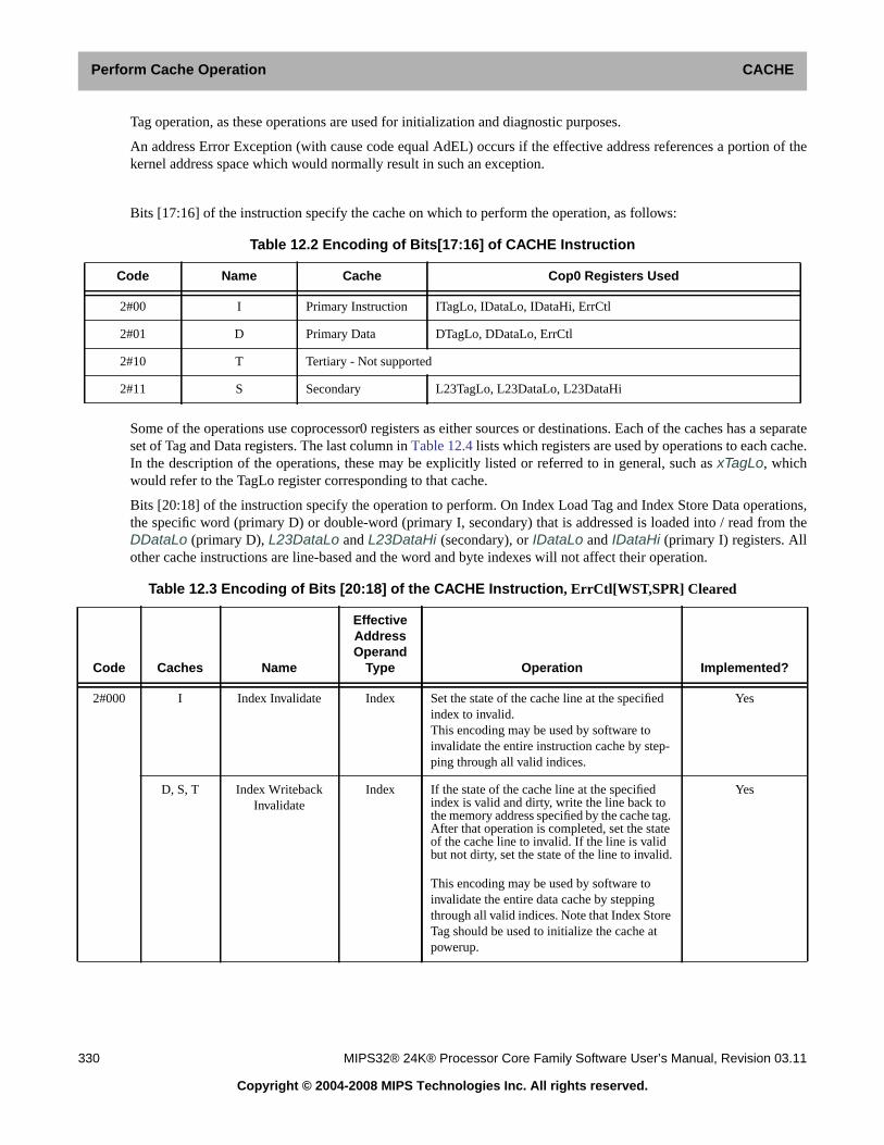
Perform Cache Operation CACHE
330 MIPS32® 24K® Processor Core Family Software User’s Manual, Revision 03.11
Copyright © 2004-2008 MIPS Technologies Inc. All rights reserved.
Tag operation, as these operations are used for initialization and diagnostic purposes.
An address Error Exception (with cause code equal AdEL) occurs if the effective address references a portion of thekernel address space which would normally result in such an exception.
Bits [17:16] of the instruction specify the cache on which to perform the operation, as follows:
Some of the operations use coprocessor0 registers as either sources or destinations. Each of the caches has a separateset of Tag and Data registers. The last column in Table 12.4 lists which registers are used by operations to each cache.In the description of the operations, these may be explicitly listed or referred to in general, such as xTagLo, whichwould refer to the TagLo register corresponding to that cache.
Bits [20:18] of the instruction specify the operation to perform. On Index Load Tag and Index Store Data operations,the specific word (primary D) or double-word (primary I, secondary) that is addressed is loaded into / read from theDDataLo (primary D), L23DataLo and L23DataHi (secondary), or IDataLo and IDataHi (primary I) registers. Allother cache instructions are line-based and the word and byte indexes will not affect their operation.
Table 12.2 Encoding of Bits[17:16] of CACHE Instruction
Code Name Cache Cop0 Registers Used
2#00 I Primary Instruction ITagLo, IDataLo, IDataHi, ErrCtl
2#01 D Primary Data DTagLo, DDataLo, ErrCtl
2#10 T Tertiary - Not supported
2#11 S Secondary L23TagLo, L23DataLo, L23DataHi
Table 12.3 Encoding of Bits [20:18] of the CACHE Instruction, ErrCtl[WST,SPR] Cleared
Code Caches Name
EffectiveAddressOperand
Type Operation Implemented?
2#000 I Index Invalidate Index Set the state of the cache line at the specifiedindex to invalid.This encoding may be used by software toinvalidate the entire instruction cache by step-ping through all valid indices.
Yes
D, S, T Index WritebackInvalidate
Index If the state of the cache line at the specifiedindex is valid and dirty, write the line back tothe memory address specified by the cache tag.After that operation is completed, set the stateof the cache line to invalid. If the line is validbut not dirty, set the state of the line to invalid.
This encoding may be used by software toinvalidate the entire data cache by steppingthrough all valid indices. Note that Index StoreTag should be used to initialize the cache atpowerup.
Yes
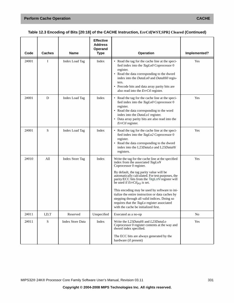
Perform Cache Operation CACHE
MIPS32® 24K® Processor Core Family Software User’s Manual, Revision 03.11 331
Copyright © 2004-2008 MIPS Technologies Inc. All rights reserved.
2#001 I Index Load Tag Index • Read the tag for the cache line at the speci-fied index into the TagLo0 Coprocessor 0register.
• Read the data corresponding to the dwordindex into the DataLo0 and DataHi0 regis-ters.
• Precode bits and data array parity bits arealso read into the ErrCtl register.
Yes
2#001 D Index Load Tag Index • Read the tag for the cache line at the speci-fied index into the TagLo0 Coprocessor 0register.
• Read the data corresponding to the wordindex into the DataLo1 register.
• Data array parity bits are also read into theErrCtl register.
Yes
2#001 S Index Load Tag Index • Read the tag for the cache line at the speci-fied index into the TagLo2 Coprocessor 0register.
• Read the data corresponding to the dwordindex into the L23DataLo and L23DataHiregisters.
Yes
2#010 All Index Store Tag Index Write the tag for the cache line at the specifiedindex from the associated TagLoNCoprocessor 0 register.
By default, the tag parity value will beautomatically calculated. For test purposes, theparity/ECC bits from the TagLoN register willbe used if ErrCtlPO is set.
This encoding may be used by software to ini-tialize the entire instruction or data caches bystepping through all valid indices. Doing sorequires that the TagLo register associatedwith the cache be initialized first.
Yes
2#011 I,D,T Reserved Unspecified Executed as a no-op No
2#011 S Index Store Data Index Write the L23DataHi and L23DataLoCoprocessor 0 register contents at the way anddword index specified.
The ECC bits are always generated by thehardware (if present)
Yes
Table 12.3 Encoding of Bits [20:18] of the CACHE Instruction, ErrCtl[WST,SPR] Cleared (Continued)
Code Caches Name
EffectiveAddressOperand
Type Operation Implemented?

Perform Cache Operation CACHE
332 MIPS32® 24K® Processor Core Family Software User’s Manual, Revision 03.11
Copyright © 2004-2008 MIPS Technologies Inc. All rights reserved.
2#100 All Hit Invalidate Address If the cache line contains the specified address,set the state of the cache line to invalid.This encoding may be used by software toinvalidate a range of addresses from theinstruction cache by stepping through theaddress range by the line size of the cache.
Yes
2#101 I Fill Address Fill the cache from the specified address.
The cache line is refetched even if it is alreadyin the cache.
Yes
D, S, T Hit WriteBackInvalidate
Address If the cache line contains the specified addressand it is valid and dirty, write the contents backto memory. After that operation is completed,set the state of the cache line to invalid. If theline is valid but not dirty, set the state of the lineto invalid.
This encoding may be used by software toinvalidate a range of addresses from the datacache by stepping through the address rangeby the line size of the cache.
Yes
2#110 D, S, T Hit WriteBack Address If the cache line contains the specified addressand it is valid and dirty, write the contents backto memory. After the operation is completed,leave the state of the line valid, but clear thedirty state.
Yes
2#111 All Fetch and Lock Address If the cache does not contain the specifiedaddress, fill it from memory, performing awriteback if required, and set the state to validand locked. If the cache already contains thespecified address, set the state to locked. Theway selected on fill from memory is the leastrecently used.
The lock state is cleared by executing an IndexInvalidate, Index Writeback Invalidate, HitInvalidate, or Hit Writeback Invalidateoperation to the locked line, or via an IndexStore Tag operation with the lock bit reset inthe xTagLo register.
It is illegal to lock all ways at a given cacheindex. If all ways are locked, subsequentreferences to that index will displace one of thelocked lines.
Yes
Table 12.3 Encoding of Bits [20:18] of the CACHE Instruction, ErrCtl[WST,SPR] Cleared (Continued)
Code Caches Name
EffectiveAddressOperand
Type Operation Implemented?
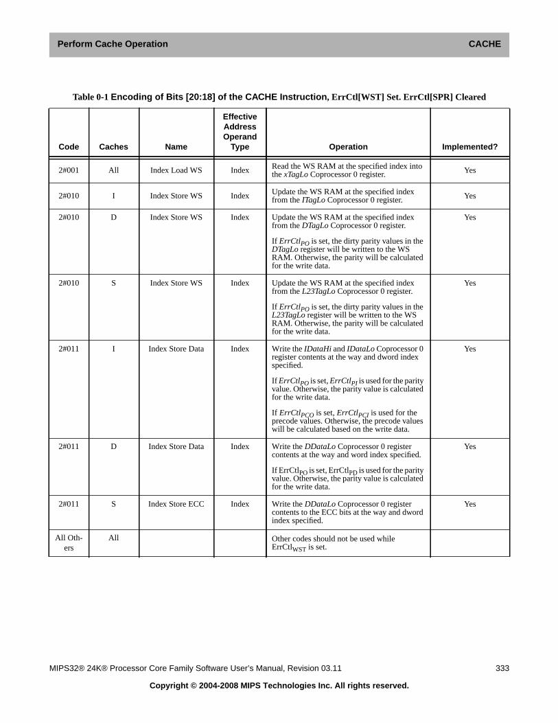
Perform Cache Operation CACHE
MIPS32® 24K® Processor Core Family Software User’s Manual, Revision 03.11 333
Copyright © 2004-2008 MIPS Technologies Inc. All rights reserved.
Table 0-1 Encoding of Bits [20:18] of the CACHE Instruction, ErrCtl[WST] Set. ErrCtl[SPR] Cleared
Code Caches Name
EffectiveAddressOperand
Type Operation Implemented?
2#001 All Index Load WS Index Read the WS RAM at the specified index intothe xTagLo Coprocessor 0 register. Yes
2#010 I Index Store WS Index Update the WS RAM at the specified indexfrom the ITagLo Coprocessor 0 register. Yes
2#010 D Index Store WS Index Update the WS RAM at the specified indexfrom the DTagLo Coprocessor 0 register.
If ErrCtlPO is set, the dirty parity values in theDTagLo register will be written to the WSRAM. Otherwise, the parity will be calculatedfor the write data.
Yes
2#010 S Index Store WS Index Update the WS RAM at the specified indexfrom the L23TagLo Coprocessor 0 register.
If ErrCtlPO is set, the dirty parity values in theL23TagLo register will be written to the WSRAM. Otherwise, the parity will be calculatedfor the write data.
Yes
2#011 I Index Store Data Index Write the IDataHi and IDataLo Coprocessor 0register contents at the way and dword indexspecified.
If ErrCtlPO is set, ErrCtlPI is used for the parityvalue. Otherwise, the parity value is calculatedfor the write data.
If ErrCtlPCO is set, ErrCtlPCI is used for theprecode values. Otherwise, the precode valueswill be calculated based on the write data.
Yes
2#011 D Index Store Data Index Write the DDataLo Coprocessor 0 registercontents at the way and word index specified.
If ErrCtlPO is set, ErrCtlPD is used for the parityvalue. Otherwise, the parity value is calculatedfor the write data.
Yes
2#011 S Index Store ECC Index Write the DDataLo Coprocessor 0 registercontents to the ECC bits at the way and dwordindex specified.
Yes
All Oth-ers
All Other codes should not be used whileErrCtlWST is set.

Perform Cache Operation CACHE
334 MIPS32® 24K® Processor Core Family Software User’s Manual, Revision 03.11
Copyright © 2004-2008 MIPS Technologies Inc. All rights reserved.
Restrictions:
The operation of this instruction is UNDEFINED for any operation/cache combination that is not implemented.
The operation of this instruction is UNDEFINED if the operation requires an address, and that address is uncache-able.
If access to Coprocessor 0 is not enabled, a Coprocessor Unusable Exception is signaled.
Operation:
vAddr ← GPR[base] + sign_extend(offset)(pAddr, uncached) ← AddressTranslation(vAddr, DataReadReference)CacheOp(op, vAddr, pAddr)
Exceptions:
TLB Refill Exception.
TLB Invalid Exception
Coprocessor Unusable Exception
Address Error Exception
Cache Error Exception
Bus Error Exception
Table 12.4 Encoding of Bits [20:18] of the CACHE Instruction, ErrCtl[SPR] Set, ErrCtl[WST] Cleared
Code Caches Name
EffectiveAddressOperand
Type Operation Implemented?
2#001 I Index Load Tag Index Read the SPRAM tag at the specified indexinto the ITagLo Coprocessor 0 register. Alsoread the instruction data and precodeinformation corresponding to the byte indexinto the IDataHi,IDataLo, and ErrCtl registers
Yes
2#001 D Index Load Tag Index Read the SPRAM tag at the specified indexinto the DTagLo Coprocessor 0 register.
Yes
2#010 I, D Index Store Tag Index Update the SPRAM tag at the specified indexfrom the xTagLo Coprocessor 0 register.
Yes
2#011 I Index Store Data Index Write the IDataLo and IDataHi Coprocessor 0register contents into the SPRAM at the dwordindex specified.
Yes
2#011 D Index Store Data Index Write the DDataLo Coprocessor 0 registercontents into the SPRAM at the word indexspecified.
Yes
All Oth-ers
I,D Other codes should not be used whileErrCtlSPR is set.
All S,T Secondary and Tertiary operations should notbe performed while ErrCtlSPR is set.

Load Linked Word ILL
MIPS32® 24K® Processor Core Family Software User’s Manual, Revision 03.11 335
Copyright © 2004-2008 MIPS Technologies Inc. All rights reserved.
Format: LL rt, offset(base) MIPS32
Purpose: Load Linked Word
To load a word from memory for an atomic read-modify-write
Description: GPR[rt] ← memory[GPR[base] + offset]
The LL and SC instructions provide the primitives to implement atomic read-modify-write (RMW) operations forsynchronizable memory locations.
The contents of the 32-bit word at the memory location specified by the aligned effective address are fetched andwritten into GPR rt. The 16-bit signed offset is added to the contents of GPR base to form an effective address.
This begins a RMW sequence on the current processor. There can be only one active RMW sequence per processor.When an LL is executed it starts an active RMW sequence replacing any other sequence that was active. The RMWsequence is completed by a subsequent SC instruction that either completes the RMW sequence atomically and suc-ceeds, or does not and fails.
Executing LL on one processor does not cause an action that, by itself, causes an SC for the same block to fail onanother processor.
An execution of LL does not have to be followed by execution of SC; a program is free to abandon the RMWsequence without attempting a write.
Restrictions:
The addressed location must be synchronizable by all processors and I/O devices sharing the location; if it is not, theresult in UNPREDICTABLE. Which storage is synchronizable is a function of both CPU and system implementa-tions. See the documentation of the SC instruction for the formal definition.
The effective address must be naturally-aligned. If either of the 2 least-significant bits of the effective address is non-zero, an Address Error exception occurs.
Operation:
vAddr ← sign_extend(offset) + GPR[base]if vAddr1..0 ≠ 02 then
SignalException(AddressError)endif(pAddr, CCA) ← AddressTranslation (vAddr, DATA, LOAD)memword ← LoadMemory (CCA, WORD, pAddr, vAddr, DATA)GPR[rt] ← memwordLLbit ← 1
Exceptions:
TLB Refill, TLB Invalid, Address Error, Reserved Instruction, Watch
Programming Notes:
There is no Load Linked Word Unsigned operation corresponding to Load Word Unsigned.
31 26 25 21 20 16 15 0
LL110000
base rt offset
6 5 5 16
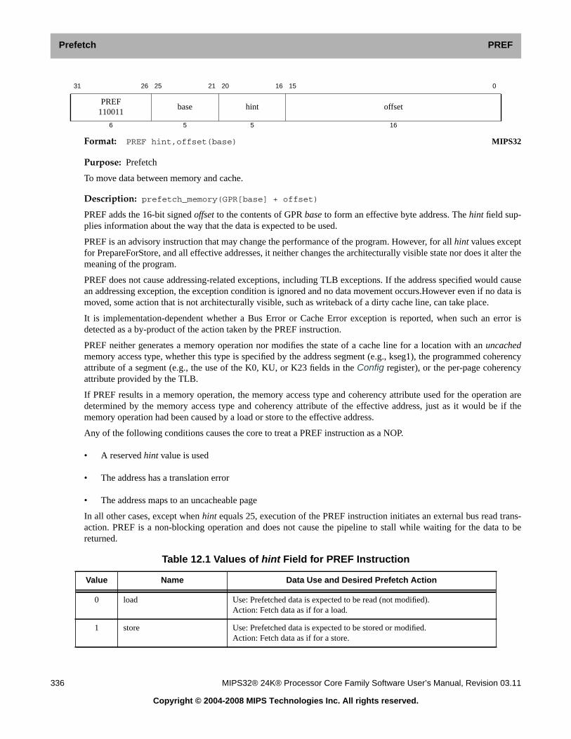
Prefetch PREF
336 MIPS32® 24K® Processor Core Family Software User’s Manual, Revision 03.11
Copyright © 2004-2008 MIPS Technologies Inc. All rights reserved.
Format: PREF hint,offset(base) MIPS32
Purpose: Prefetch
To move data between memory and cache.
Description: prefetch_memory(GPR[base] + offset)
PREF adds the 16-bit signed offset to the contents of GPR base to form an effective byte address. The hint field sup-plies information about the way that the data is expected to be used.
PREF is an advisory instruction that may change the performance of the program. However, for all hint values exceptfor PrepareForStore, and all effective addresses, it neither changes the architecturally visible state nor does it alter themeaning of the program.
PREF does not cause addressing-related exceptions, including TLB exceptions. If the address specified would causean addressing exception, the exception condition is ignored and no data movement occurs.However even if no data ismoved, some action that is not architecturally visible, such as writeback of a dirty cache line, can take place.
It is implementation-dependent whether a Bus Error or Cache Error exception is reported, when such an error isdetected as a by-product of the action taken by the PREF instruction.
PREF neither generates a memory operation nor modifies the state of a cache line for a location with an uncachedmemory access type, whether this type is specified by the address segment (e.g., kseg1), the programmed coherencyattribute of a segment (e.g., the use of the K0, KU, or K23 fields in the Config register), or the per-page coherencyattribute provided by the TLB.
If PREF results in a memory operation, the memory access type and coherency attribute used for the operation aredetermined by the memory access type and coherency attribute of the effective address, just as it would be if thememory operation had been caused by a load or store to the effective address.
Any of the following conditions causes the core to treat a PREF instruction as a NOP.
• A reserved hint value is used
• The address has a translation error
• The address maps to an uncacheable page
In all other cases, except when hint equals 25, execution of the PREF instruction initiates an external bus read trans-action. PREF is a non-blocking operation and does not cause the pipeline to stall while waiting for the data to bereturned.
31 26 25 21 20 16 15 0
PREF110011
base hint offset
6 5 5 16
Table 12.1 Values of hint Field for PREF Instruction
Value Name Data Use and Desired Prefetch Action
0 load Use: Prefetched data is expected to be read (not modified).Action: Fetch data as if for a load.
1 store Use: Prefetched data is expected to be stored or modified.Action: Fetch data as if for a store.

Prefetch IPREF
MIPS32® 24K® Processor Core Family Software User’s Manual, Revision 03.11 337
Copyright © 2004-2008 MIPS Technologies Inc. All rights reserved.
Restrictions:
None
Operation:
vAddr ← GPR[base] + sign_extend(offset)(pAddr, CCA) ← AddressTranslation(vAddr, DATA, LOAD)
2-3 Reserved Reserved - treated as a NOP.
4 load_streamed Use: Prefetched data is expected to be read (not modified) but not reusedextensively; it “streams” through cache.Action: Fetch data as if for a store. LRU replacement information is ignoredand data is placed in way 0 of the cache, so it will be displaced by otherstreamed prefetches and not displace retained prefetches. If way 0 is locked,the prefetch will be dropped.
5 store_streamed Use: Prefetched data is expected to be stored or modified but not reusedextensively; it “streams” through cache.Action: Fetch data as if for a store. LRU replacement information is ignoredand data is placed in way 0 of the cache, so it will be displaced by otherstreamed prefetches and not displace retained prefetches. If way 0 is locked,the prefetch will be dropped.
6 load_retained Use: Prefetched data is expected to be read (not modified) and reused exten-sively; it should be “retained” in the cache.Action: Fetch data as if for a load. LRU replacement information is used, butway 0 of the cache is specifically excluded. This prevents streamedprefetches from displacing the line.
7 store_retained Use: Prefetched data is expected to be stored or modified and reused exten-sively; it should be “retained” in the cache.Action: Fetch data as if for a store. LRU replacement information is used, butway 0 of the cache is specifically excluded. This prevents streamedprefetches from displacing the line.
8-24 Reserved Reserved - treated as a NOP.
25 writeback_invalidate (alsoknown as “nudge”)
Use: Data is no longer expected to be used.Action: Schedule a writeback of any dirty data. The cache line is marked asinvalid upon completion of the writeback. If cache line is clean or locked, noaction is taken.
26-29 Reserved Reserved - treated as a NOP.
30 PrepareForStore Use: Prepare the cache for writing an entire line, without the overheadinvolved in filling the line from memory.Action: If the reference hits in the cache, no action is taken. If the referencemisses in the cache, a line is selected for replacement, any valid and dirtyvictim is written back to memory, the entire line is filled with zero data, andthe state of the line is marked as valid and dirty.Programming Note: Because the cache line is filled with zero data only on acache miss, software must not assume that this action, in and of itself, can beused as a fast bzero-type function.
31 Reserved Reserved - treated as a NOP.
Table 12.1 Values of hint Field for PREF Instruction
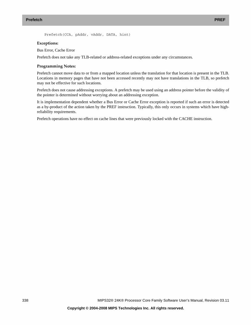
Prefetch PREF
338 MIPS32® 24K® Processor Core Family Software User’s Manual, Revision 03.11
Copyright © 2004-2008 MIPS Technologies Inc. All rights reserved.
Prefetch(CCA, pAddr, vAddr, DATA, hint)
Exceptions:
Bus Error, Cache Error
Prefetch does not take any TLB-related or address-related exceptions under any circumstances.
Programming Notes:
Prefetch cannot move data to or from a mapped location unless the translation for that location is present in the TLB.Locations in memory pages that have not been accessed recently may not have translations in the TLB, so prefetchmay not be effective for such locations.
Prefetch does not cause addressing exceptions. A prefetch may be used using an address pointer before the validity ofthe pointer is determined without worrying about an addressing exception.
It is implementation dependent whether a Bus Error or Cache Error exception is reported if such an error is detectedas a by-product of the action taken by the PREF instruction. Typically, this only occurs in systems which have high-reliability requirements.
Prefetch operations have no effect on cache lines that were previously locked with the CACHE instruction.

Store Conditional Word ISC
MIPS32® 24K® Processor Core Family Software User’s Manual, Revision 03.11 339
Copyright © 2004-2008 MIPS Technologies Inc. All rights reserved.
Format: SC rt, offset(base) MIPS32
Purpose: Store Conditional Word
To store a word to memory to complete an atomic read-modify-write
Description: if atomic_update then memory[GPR[base] + offset] ← GPR[rt], GPR[rt] ← 1else GPR[rt] ← 0
The LL and SC instructions provide primitives to implement atomic read-modify-write (RMW) operations for syn-chronizable memory locations.
The 32-bit word in GPR rt is conditionally stored in memory at the location specified by the aligned effective address.The 16-bit signed offset is added to the contents of GPR base to form an effective address.
The SC completes the RMW sequence begun by the preceding LL instruction executed on the processor. To completethe RMW sequence atomically, the following occur:
• The 32-bit word of GPR rt is stored into memory at the location specified by the aligned effective address.
• A 1, indicating success, is written into GPR rt.
Otherwise, memory is not modified and a 0, indicating failure, is written into GPR rt.
If any of the following events occurs between the execution of LL and SC, the SC fails:
• An ERET instruction is executed.
If either of the following events occurs between the execution of LL and SC, the SC may succeed or it may fail; thesuccess or failure is not predictable. Portable programs should not cause one of these events.
• A memory access instruction (load, store, or prefetch) is executed on the processor executing the LL/SC.
• The instructions executed starting with the LL and ending with the SC do not lie in a 2048-byte contiguousregion of virtual memory. (The region does not have to be aligned, other than the alignment required for instruc-tion words.)
The following conditions must be true or the result of the SC is UNPREDICTABLE:
• Execution of SC must have been preceded by execution of an LL instruction.
• An RMW sequence executed without intervening events that would cause the SC to fail must use the sameaddress in the LL and SC. The address is the same if the virtual address, physical address, and cache-coherencealgorithm are identical.
Restrictions:
The effective address must be naturally-aligned. If either of the 2 least-significant bits of the address is non-zero, anAddress Error exception occurs.
Operation:
vAddr ← sign_extend(offset) + GPR[base]
31 26 25 21 20 16 15 0
SC111000
base rt offset
6 5 5 16

Store Conditional Word SC
340 MIPS32® 24K® Processor Core Family Software User’s Manual, Revision 03.11
Copyright © 2004-2008 MIPS Technologies Inc. All rights reserved.
if vAddr1..0 ≠ 02 thenSignalException(AddressError)
endif(pAddr, CCA) ← AddressTranslation (vAddr, DATA, STORE)dataword ← GPR[rt]if LLbit then
StoreMemory (CCA, WORD, dataword, pAddr, vAddr, DATA)endifGPR[rt] ← 031 || LLbit
Exceptions:
TLB Refill, TLB Invalid, TLB Modified, Address Error, Watch
Programming Notes:
LL and SC are used to atomically update memory locations, as shown below.
L1:LL T1, (T0) # load counterADDI T2, T1, 1 # incrementSC T2, (T0) # try to store, checking for atomicityBEQ T2, 0, L1 # if not atomic (0), try againNOP # branch-delay slot
Exceptions between the LL and SC cause SC to fail, so persistent exceptions must be avoided. Some examples ofthese are arithmetic operations that trap, system calls, and floating point operations that trap or require software emu-lation assistance.
LL and SC function on a single processor for cached noncoherent memory so that parallel programs can be run onuniprocessor systems that do not support cached coherent memory access types.

ISYNC
MIPS32® 24K® Processor Core Family Software User’s Manual, Revision 03.11 341
Copyright © 2004-2008 MIPS Technologies Inc. All rights reserved.
Format: SYNC (stype = 0 implied) MIPS32
Purpose: To order loads and stores for shared memory.
Description:
These types of ordering guarantees are available through the SYNC instruction:
• Completion Barriers
• Ordering Barriers
Simple Description for Completion Barrier:
• The specified memory instructions (loads or stores or both) that occur before the SYNC instruction must becompleted before the specified memory instructions after the SYNC are allowed to start.
• Loads are completed when the destination register is written. Stores are completed when the stored value isvisible to every other processor in the system.
Detailed Description for Completion Barrier:
• Every synchronizable specified memory instruction (loads or stores or both) that occurs in the instructionstream before the SYNC instruction must be already globally performed before any synchronizable specifiedmemory instruction that occurs after the SYNC are allowed to be performed, with respect to any other pro-cessor or coherent I/O module.
• The barrier does not guarantee the order in which instruction fetches are performed.
• A stype value of zero will always be defined such that it performs the most complete set of synchronizationoperations that are defined. This means stype zero always does a completion barrier that affects both loadsand stores preceding the SYNC instruction and both loads and stores that are subsequent to the SYNCinstruction. Non-zero values of stype may be defined by the architecture or specific implementations to per-form synchronization behaviors that are less complete than that of stype zero. If an implementation does notuse one of these non-zero values to define a different synchronization behavior , then that non-zero value ofstype must act the same as stype zero completion barrier. This allows software written for an implementationwith a lighter-weight barrier to work on another implementation which only implements the stype zero com-pletion barrier.
• A completion barrier is required, potentially in conjunction with SSNOP (in Release 1 of the Architecture)or EHB (in Release 2 of the Architecture), to guarantee that memory reference results are visible acrossoperating mode changes. For example, a completion barrier is required on entry to and exit from DebugMode to guarantee that memory affects are handled correctly.
Completion Barrier Types:
All completion barrier types will flush any pending writes and potentially generate an external SYNC request. An
31 26 25 21 20 16 15 11 10 6 5 0
SPECIAL000000
000 0000 0000 0000 0
stypeSYNC001111
6 15 5 6

SYNC
342 MIPS32® 24K® Processor Core Family Software User’s Manual, Revision 03.11
Copyright © 2004-2008 MIPS Technologies Inc. All rights reserved.
external SYNC request will be sent if Config7ES = 1 and SI_SyncTxEn = 1. The first term is a software enable forexternalizing SYNCs and the second term is a hardware enable, indicating that the next level device (L2 or system)supports SYNC transactions. The core will wait for all pending reads to complete as well as the SYNC response if itwas externalized.
• 0x2 - Implementation specific stype. Intervention SYNC. When coherence is enabled, this SYNC will gen-erate a CoherentSync request. The CoherenceManager will respond to the SYNC when the interventions forall older coherent requests have been completed. If coherence is not enabled, will default to stype 0x0.
• 0x3 - Implementation specific style. Memory SYNC. When coherence is enabled, this SYNC will also gen-erate a CoherentSync request. When interventions for all older coherent requests have completed, the syncwill be sent to memory interface unit. All pending transactions will be sent out. If the next level device (L2or system) supports legacy SYNC transactions, as indicated by SyncTxEn = 1, an external SYNC requestwill also be generated. The CM will send a response to the core when all prior requests have completed anda SYNC response is received (if it was externalized).
• 0x0 - If coherence is enabled, this will be mapped to either a type 0x2 or 0x3 based on the value of the SYN-CCTL bit in the CM Control GCR. If coherence is not enabled, a legacy SYNC request will be generated.This will bypass the intervention pipeline in the CM and go directly to the memory unit. If SyncTxEn = 1,an external SYNC request will be generated.
Simple Description for Ordering Barrier:
• The specified memory instructions (loads or stores or both) that occur before the SYNC instruction mustalways be ordered before the specified memory instructions after the SYNC.
• Memory instructions which are ordered before other memory instructions are processed by the load/storedatapath first before the other memory instructions.
Detailed Description for Ordering Barrier:
• Every synchronizable specified memory instruction (loads or stores or both) that occurs in the instructionstream before the SYNC instruction must reach a stage in the load/store datapath after which no instructionre-ordering is possible before any synchronizable specified memory instruction which occurs after theSYNC instruction in the instruction stream reaches the same stage in the load/store datapath.
• If any memory instruction before the SYNC instruction in program order, generates a memory request to theexternal memory and any memory instruction after the SYNC instruction in program order also generates amemory request to external memory, the memory request belonging to the older instruction must be globallyperformed before the time the memory request belonging to the younger instruction is globally performed.
• The barrier does not guarantee the order in which instruction fetches are performed.
As compared to the completion barrier, the ordering barrier is a lighter-weight operation as it does not require thespecified instructions before the SYNC to be already completed. Instead it only requires that those specified instruc-tions which are subsequent to the SYNC in the instruction stream are never re-ordered for processing ahead of thespecified instructions which are before the SYNC in the instruction stream. This potentially reduces how many cyclesthe barrier instruction must stall before it completes.
The Acquire and Release barrier types are used to minimize the memory orderings that must be maintained and stillhave software synchronization work.

ISYNC
MIPS32® 24K® Processor Core Family Software User’s Manual, Revision 03.11 343
Copyright © 2004-2008 MIPS Technologies Inc. All rights reserved.
Because the core processes loads and stores in order, ordering barriers are much lighter weight. The core handles allordering barriers identically. The LSU will complete any pending evictions and the BIU will stop merging on allWBB entries. No external request will be generated and the core will not wait for pending transactions to complete.
For the purposes of this description, the CACHE, PREF and PREFX instructions are treated as loads and stores. Thatis, these instructions and the memory transactions sourced by these instructions obey the ordering and completionrules of the SYNC instruction.
Table 12.1 lists the available completion barrier and ordering barriers behaviors that can be specified using the stypefield..
Table 12.1 Encodings of the Bits[10:6] of the SYNC instruction; the SType Field
Code Name
Older instructionswhich must reach
the load/storeordering point
before the SYNCinstructioncompletes.
Youngerinstructions
which must reachthe load/storeordering pointonly after the
SYNC instructioncompletes.
Older instructionswhich must be
globallyperformed when
the SYNCinstructioncompletes
0x0 SYNCor
SYNC(0)
Loads, Stores Loads, Stores Loads, Stores
0x2 SYNC(2)Intervention Sync
Load,Stores Loads, Stores Loads, Stores
0x3 SYNC(3)Memory Sync
Load,Stores Loads, Stores Loads, Stores
0x4 SYNC_WMBor
SYNC(4)
Stores Stores
0x10 SYNC_MBor
SYNC(16)
Loads, Stores Loads, Stores
0x11 SYNC_ACQUIREor
SYNC(17)
Loads Loads, Stores
0x12 SYNC_RELEASEor
SYNC(18)
Loads, Stores Stores
0x13 SYNC_RMBor
SYNC(19)
Loads Loads
0x1,0x5-0xF,0x14 -0x1F
RESERVED
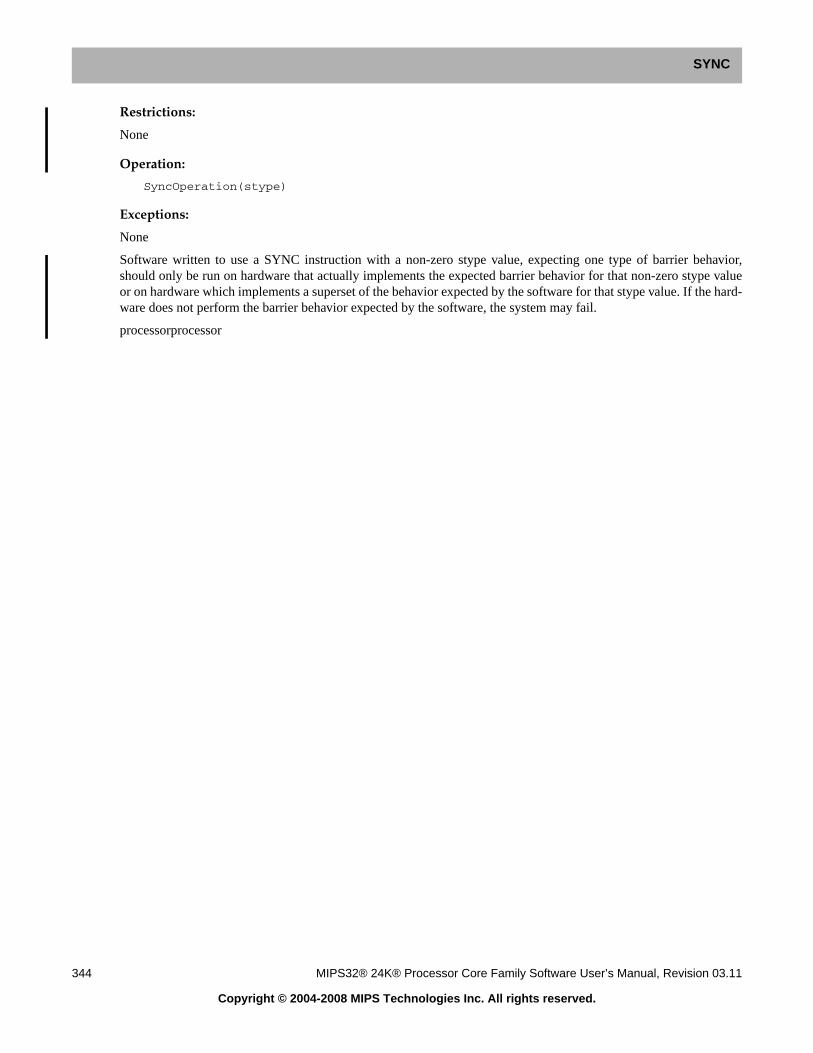
SYNC
344 MIPS32® 24K® Processor Core Family Software User’s Manual, Revision 03.11
Copyright © 2004-2008 MIPS Technologies Inc. All rights reserved.
Restrictions:
None
Operation:
SyncOperation(stype)
Exceptions:
None
Software written to use a SYNC instruction with a non-zero stype value, expecting one type of barrier behavior,should only be run on hardware that actually implements the expected barrier behavior for that non-zero stype valueor on hardware which implements a superset of the behavior expected by the software for that stype value. If the hard-ware does not perform the barrier behavior expected by the software, the system may fail.
processorprocessor

Read Indexed TLB Entry ITLBR
MIPS32® 24K® Processor Core Family Software User’s Manual, Revision 03.11 345
Copyright © 2004-2008 MIPS Technologies Inc. All rights reserved.
Format: TLBR MIPS32
Purpose: Read Indexed TLB Entry
To read an entry from the TLB.
Description:
The EntryHi, EntryLo0, EntryLo1, and PageMask registers are loaded with the contents of the TLB entry pointedto by the Index register. In Release 1 of the Architecture, it is implementation dependent whether multiple TLBmatches are detected on a TLBR. However, implementations are strongly encouraged to report multiple TLB matchesonly on a TLB write. In Release 2 of the Architecture, multiple TLB matches may only be reported on a TLB write.Note that the value written to the EntryHi, EntryLo0, and EntryLo1 registers may be different from that originallywritten to the TLB via these registers in that:
• The value returned in the G bit in both the EntryLo0 and EntryLo1 registers comes from the single G bit in theTLB entry. Recall that this bit was set from the logical AND of the two G bits in EntryLo0 and EntryLo1 whenthe TLB was written.
Restrictions:
The operation is UNDEFINED if the contents of the Index register are greater than or equal to the number of TLBentries in the processor.
If access to Coprocessor 0 is not enabled, a Coprocessor Unusable Exception is signaled.
Operation:
i ← Indexif i > (TLBEntries - 1) then
UNDEFINEDendifPageMaskMask ← TLB[i]MaskEntryHi ←
TLB[i]VPN2 ||05 || TLB[i]ASID
EntryLo1 ← 02 ||TLB[i]PFN1 ||TLB[i]C1 || TLB[i]D1 || TLB[i]V1 || TLB[i]G
EntryLo0 ← 02 ||TLB[i]PFN0 ||TLB[i]C0 || TLB[i]D0 || TLB[i]V0 || TLB[i]G
Exceptions:
Coprocessor Unusable
31 26 25 24 6 5 0
COP0010000
CO1
0000 0000 0000 0000 0000
TLBR000001
6 1 19 6

Write Indexed TLB Entry TLBWI
346 MIPS32® 24K® Processor Core Family Software User’s Manual, Revision 03.11
Copyright © 2004-2008 MIPS Technologies Inc. All rights reserved.
Format: TLBWI MIPS32
Purpose: Write Indexed TLB Entry
To write a TLB entry indexed by the Index register.
Description:
The TLB entry pointed to by the Index register is written from the contents of the EntryHi, EntryLo0, EntryLo1, andPageMask registers. It is implementation dependent whether multiple TLB matches are detected on a TLBWI. Insuch an instance, a Machine Check Exception is signaled. See Section 4.4.1 “Hits, Misses, and Multiple Matches”for the cases in which a 24K core will signal a Machine Check. The information written to the TLB entry may be dif-ferent from that in the EntryHi, EntryLo0, and EntryLo1 registers, in that:
• The single G bit in the TLB entry is set from the logical AND of the G bits in the EntryLo0 and EntryLo1 regis-ters.
Restrictions:
The operation is UNDEFINED if the contents of the Index register are greater than or equal to the number of TLBentries in the processor.
If access to Coprocessor 0 is not enabled, a Coprocessor Unusable Exception is signaled.
Operation:
i ← IndexTLB[i]Mask ← PageMaskMaskTLB[i]VPN2 ← EntryHiVPN2TLB[i]ASID ← EntryHiASIDTLB[i]G ← EntryLo1G and EntryLo0GTLB[i]PFN1 ← EntryLo1PFNTLB[i]C1 ← EntryLo1CTLB[i]D1 ← EntryLo1DTLB[i]V1 ← EntryLo1VTLB[i]PFN0 ← EntryLo0PFNTLB[i]C0 ← EntryLo0CTLB[i]D0 ← EntryLo0DTLB[i]V0 ← EntryLo0V
Exceptions:
Coprocessor Unusable
Machine Check
31 26 25 24 6 5 0
COP0010000
CO1
0000 0000 0000 0000 0000
TLBWI000010
6 1 19 6
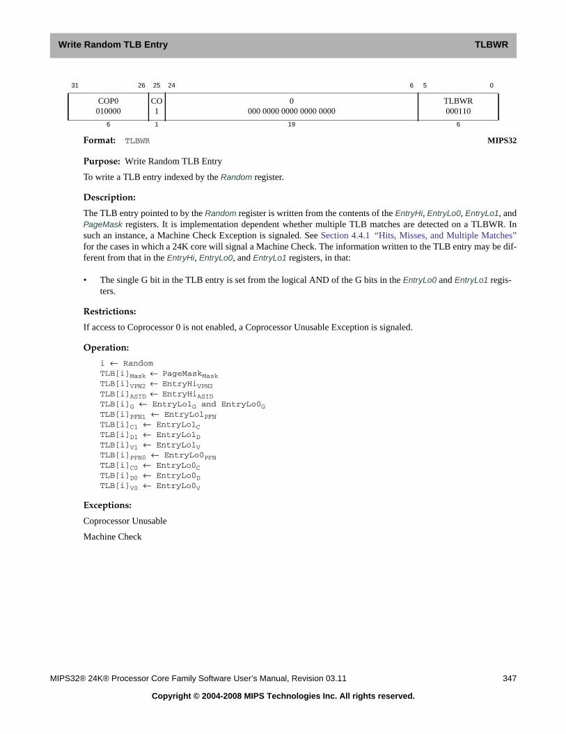
Write Random TLB Entry ITLBWR
MIPS32® 24K® Processor Core Family Software User’s Manual, Revision 03.11 347
Copyright © 2004-2008 MIPS Technologies Inc. All rights reserved.
Format: TLBWR MIPS32
Purpose: Write Random TLB Entry
To write a TLB entry indexed by the Random register.
Description:
The TLB entry pointed to by the Random register is written from the contents of the EntryHi, EntryLo0, EntryLo1, andPageMask registers. It is implementation dependent whether multiple TLB matches are detected on a TLBWR. Insuch an instance, a Machine Check Exception is signaled. See Section 4.4.1 “Hits, Misses, and Multiple Matches”for the cases in which a 24K core will signal a Machine Check. The information written to the TLB entry may be dif-ferent from that in the EntryHi, EntryLo0, and EntryLo1 registers, in that:
• The single G bit in the TLB entry is set from the logical AND of the G bits in the EntryLo0 and EntryLo1 regis-ters.
Restrictions:
If access to Coprocessor 0 is not enabled, a Coprocessor Unusable Exception is signaled.
Operation:
i ← RandomTLB[i]Mask ← PageMaskMaskTLB[i]VPN2 ← EntryHiVPN2TLB[i]ASID ← EntryHiASIDTLB[i]G ← EntryLo1G and EntryLo0GTLB[i]PFN1 ← EntryLo1PFNTLB[i]C1 ← EntryLo1CTLB[i]D1 ← EntryLo1DTLB[i]V1 ← EntryLo1VTLB[i]PFN0 ← EntryLo0PFNTLB[i]C0 ← EntryLo0CTLB[i]D0 ← EntryLo0DTLB[i]V0 ← EntryLo0V
Exceptions:
Coprocessor Unusable
Machine Check
31 26 25 24 6 5 0
COP0010000
CO1
0000 0000 0000 0000 0000
TLBWR000110
6 1 19 6
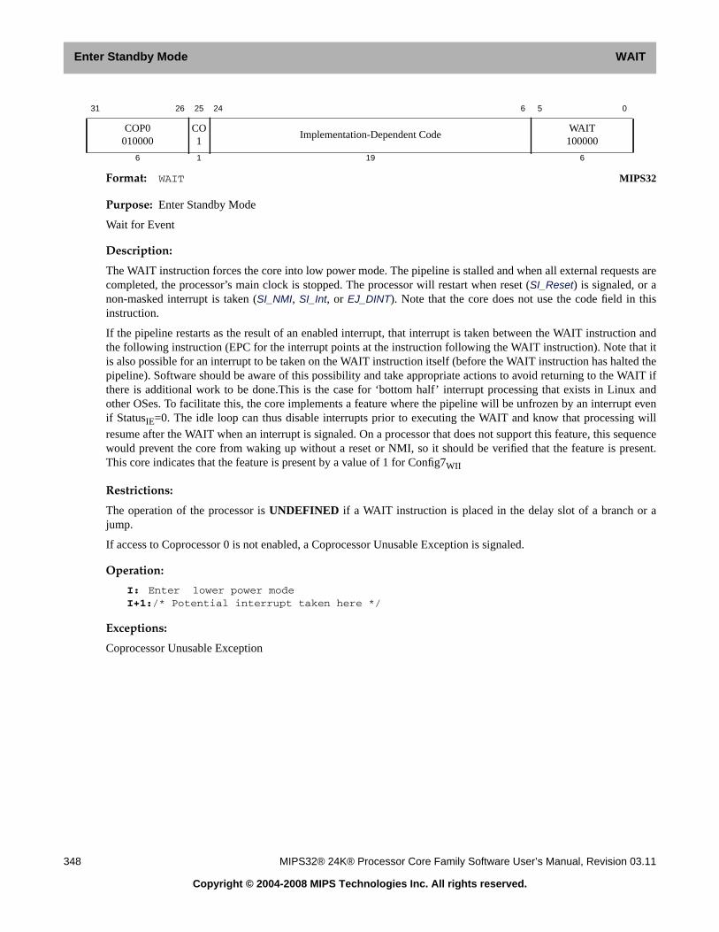
Enter Standby Mode WAIT
348 MIPS32® 24K® Processor Core Family Software User’s Manual, Revision 03.11
Copyright © 2004-2008 MIPS Technologies Inc. All rights reserved.
Format: WAIT MIPS32
Purpose: Enter Standby Mode
Wait for Event
Description:
The WAIT instruction forces the core into low power mode. The pipeline is stalled and when all external requests arecompleted, the processor’s main clock is stopped. The processor will restart when reset (SI_Reset) is signaled, or anon-masked interrupt is taken (SI_NMI, SI_Int, or EJ_DINT). Note that the core does not use the code field in thisinstruction.
If the pipeline restarts as the result of an enabled interrupt, that interrupt is taken between the WAIT instruction andthe following instruction (EPC for the interrupt points at the instruction following the WAIT instruction). Note that itis also possible for an interrupt to be taken on the WAIT instruction itself (before the WAIT instruction has halted thepipeline). Software should be aware of this possibility and take appropriate actions to avoid returning to the WAIT ifthere is additional work to be done.This is the case for ‘bottom half’ interrupt processing that exists in Linux andother OSes. To facilitate this, the core implements a feature where the pipeline will be unfrozen by an interrupt evenif StatusIE=0. The idle loop can thus disable interrupts prior to executing the WAIT and know that processing willresume after the WAIT when an interrupt is signaled. On a processor that does not support this feature, this sequencewould prevent the core from waking up without a reset or NMI, so it should be verified that the feature is present.This core indicates that the feature is present by a value of 1 for Config7WII
Restrictions:
The operation of the processor is UNDEFINED if a WAIT instruction is placed in the delay slot of a branch or ajump.
If access to Coprocessor 0 is not enabled, a Coprocessor Unusable Exception is signaled.
Operation:
I: Enter lower power modeI+1:/* Potential interrupt taken here */
Exceptions:
Coprocessor Unusable Exception
31 26 25 24 6 5 0
COP0010000
CO1
Implementation-Dependent CodeWAIT
100000
6 1 19 6

Chapter 13
MIPS32® 24K® Processor Core Family Software User’s Manual, Revision 03.11 349
Copyright © 2004-2008 MIPS Technologies Inc. All rights reserved.
MIPS16e™ Application-Specific Extension to the MIPS32®Instruction Set
This chapter describes the MIPS16e ASE as implemented in the 24K core. Refer to Volume IV-a of the MIPS32®Architecture Reference Manual [3] for a general description of the MIPS16e ASE and descriptions of the instructions.
This chapter covers the following topics:
• Section 13.1 “Instruction Bit Encoding”
• Section 13.2 “Instruction Listing”
13.1 Instruction Bit Encoding
Table 13.2 through Table 13.9 describe the encoding used for the MIPS16e ASE. Table 13.1 describes the meaningof the symbols used in the tables.
Table 13.1 Symbols Used in the Instruction Encoding Tables
Symbol Meaning
∗ Operation or field codes marked with this symbol are reserved for future use. Executing such aninstruction cause a Reserved Instruction Exception.
δ (Also italic field name.) Operation or field codes marked with this symbol denotes a field class.The instruction word must be further decoded by examining additional tables that show values foranother instruction field.
β Operation or field codes marked with this symbol represent a valid encoding for a higher-orderMIPS ISA level. Executing such an instruction cause a Reserved Instruction Exception.
θ Operation or field codes marked with this symbol are available to licensed MIPS partners. Toavoid multiple conflicting instruction definitions, the partner must notify MIPS Technologies, Inc.when one of these encodings is used. If no instruction is encoded with this value, executing such aninstruction must cause a Reserved Instruction Exception (SPECIAL2 encodings or coprocessorinstruction encodings for a coprocessor to which access is allowed) or a Coprocessor UnusableException (coprocessor instruction encodings for a coprocessor to which access is not allowed).
σ Field codes marked with this symbol represent an EJTAG support instruction and implementationof this encoding is optional for each implementation. If the encoding is not implemented, execut-ing such an instruction must cause a Reserved Instruction Exception. If the encoding is imple-mented, it must match the instruction encoding as shown in the table.
ε Operation or field codes marked with this symbol are reserved for MIPS Application SpecificExtensions. If the ASE is not implemented, executing such an instruction must cause a ReservedInstruction Exception.
φ Operation or field codes marked with this symbol are obsolete and will be removed from a futurerevision of the MIPS64 ISA. Software should avoid using these operation or field codes.
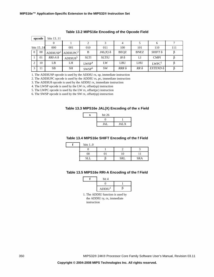
MIPS16e™ Application-Specific Extension to the MIPS32® Instruction Set
350 MIPS32® 24K® Processor Core Family Software User’s Manual, Revision 03.11
Copyright © 2004-2008 MIPS Technologies Inc. All rights reserved.
Table 13.2 MIPS16e Encoding of the Opcode Field
opcode bits 13..11
0 1 2 3 4 5 6 7
bits 15..14 000 001 010 011 100 101 110 111
0 00 ADDIUSP1
1. The ADDIUSP opcode is used by the ADDIU rx, sp, immediate instruction
ADDIUPC2
2. The ADDIUPC opcode is used by the ADDIU rx, pc, immediate instruction
B JAL(X) δ BEQZ BNEZ SHIFT δ β
1 01 RRI-A δ ADDIU83
3. The ADDIU8 opcode is used by the ADDIU rx, immediate instruction
SLTI SLTIU I8 δ LI CMPI β
2 10 LB LH LWSP4
4. The LWSP opcode is used by the LW rx, offset(sp) instruction
LW LBU LHU LWPC5
5. The LWPC opcode is used by the LW rx, offset(pc) instruction
β
3 11 SB SH SWSP6
6. The SWSP opcode is used by the SW rx, offset(sp) instruction
SW RRR δ RR δ EXTEND δ β
Table 13.3 MIPS16e JAL(X) Encoding of the x Field
x bit 26
0 1
JAL JALX
Table 13.4 MIPS16e SHIFT Encoding of the f Field
f bits 1..0
0 1 2 3
00 01 10 11
SLL β SRL SRA
Table 13.5 MIPS16e RRI-A Encoding of the f Field
f bit 4
0 1
ADDIU1
1. The ADDIU function is used bythe ADDIU ry, rx, immediateinstruction
β

13.1 Instruction Bit Encoding
MIPS32® 24K® Processor Core Family Software User’s Manual, Revision 03.11 351
Copyright © 2004-2008 MIPS Technologies Inc. All rights reserved.
Table 13.6 MIPS16e I8 Encoding of the funct Field
funct bits 10..8
0 1 2 3 4 5 6 7
000 001 010 011 100 101 110 111
BTEQZ BTNEZ SWRASP1
1. The SWRASP function is used by the SW ra, offset(sp) instruction
ADJSP2
2. The ADJSP function is used by the ADDIU sp, immediate instruction
SVRS δ MOV32R3
3. The MOV32R function is used by the MOVE r32, rz instruction
* MOVR324
4. The MOVR32 function is used by the MOVE ry, r32 instruction
Table 13.7 MIPS16e RRR Encoding of the f Field
f bits 1..0
0 1 2 3
00 01 10 11
β ADDU β SUBU
Table 13.8 MIPS16e RR Encoding of the Funct Field
funct bits 2..0
0 1 2 3 4 5 6 7
bits 4..3 000 001 010 011 100 101 110 111
0 00 J(AL)R(C) δ SDBBP SLT SLTU SLLV BREAK SRLV SRAV
1 01 β * CMP NEG AND OR XOR NOT
2 10 MFHI CNVT δ MFLO β β * β β3 11 MULT MULTU DIV DIVU β β β β
Table 13.9 MIPS16e I8 Encoding of the s Field when funct=SVRS
s bit 7
0 1
RESTORE SAVE
Table 13.10 MIPS16e RR Encoding of the ry Field when funct=J(AL)R(C)
ry bits 7..5
0 1 2 3 4 5 6 7
000 001 010 011 100 101 110 111
JR rx JR ra JALR * JRC rx JRC ra JALRC *
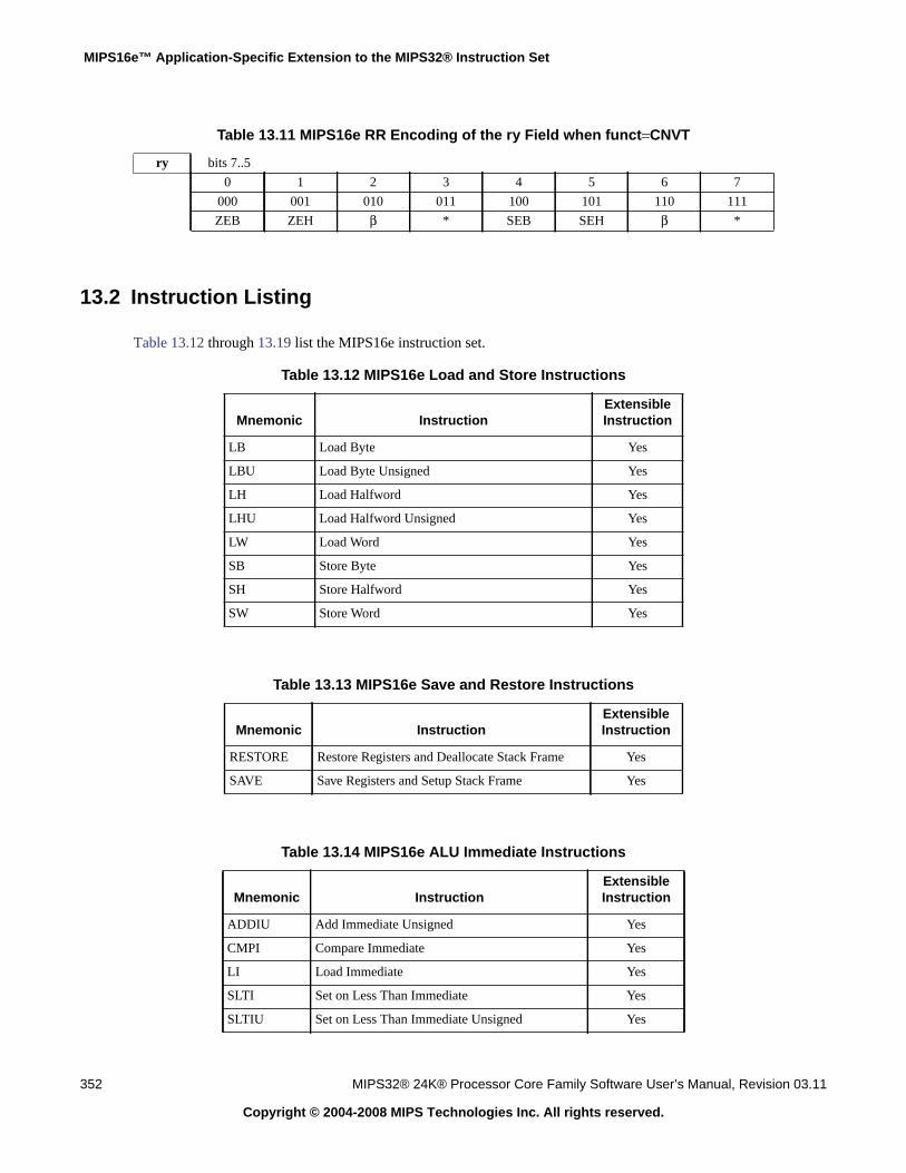
MIPS16e™ Application-Specific Extension to the MIPS32® Instruction Set
352 MIPS32® 24K® Processor Core Family Software User’s Manual, Revision 03.11
Copyright © 2004-2008 MIPS Technologies Inc. All rights reserved.
13.2 Instruction Listing
Table 13.12 through 13.19 list the MIPS16e instruction set.
Table 13.11 MIPS16e RR Encoding of the ry Field when funct=CNVT
ry bits 7..5
0 1 2 3 4 5 6 7
000 001 010 011 100 101 110 111
ZEB ZEH β * SEB SEH β *
Table 13.12 MIPS16e Load and Store Instructions
Mnemonic InstructionExtensibleInstruction
LB Load Byte Yes
LBU Load Byte Unsigned Yes
LH Load Halfword Yes
LHU Load Halfword Unsigned Yes
LW Load Word Yes
SB Store Byte Yes
SH Store Halfword Yes
SW Store Word Yes
Table 13.13 MIPS16e Save and Restore Instructions
Mnemonic InstructionExtensibleInstruction
RESTORE Restore Registers and Deallocate Stack Frame Yes
SAVE Save Registers and Setup Stack Frame Yes
Table 13.14 MIPS16e ALU Immediate Instructions
Mnemonic InstructionExtensibleInstruction
ADDIU Add Immediate Unsigned Yes
CMPI Compare Immediate Yes
LI Load Immediate Yes
SLTI Set on Less Than Immediate Yes
SLTIU Set on Less Than Immediate Unsigned Yes

13.2 Instruction Listing
MIPS32® 24K® Processor Core Family Software User’s Manual, Revision 03.11 353
Copyright © 2004-2008 MIPS Technologies Inc. All rights reserved.
Table 13.15 MIPS16e Arithmetic Two or Three Operand Register Instructions
Mnemonic InstructionExtensibleInstruction
ADDU Add Unsigned No
AND AND No
CMP Compare No
MOVE Move No
NEG Negate No
NOT Not No
OR OR No
SEB Sign-Extend Byte No
SEH Sign-Extend Halfword No
SLT Set on Less Than No
SLTU Set on Less Than Unsigned No
SUBU Subtract Unsigned No
XOR Exclusive OR No
ZEB Zero-Extend Byte No
ZEH Zero-Extend Halfword No
Table 13.16 MIPS16e Special Instructions
Mnemonic InstructionExtensibleInstruction
BREAK Breakpoint No
SDBBP Software Debug Breakpoint No
EXTEND Extend No
Table 13.17 MIPS16e Multiply and Divide Instructions
Mnemonic InstructionExtensibleInstruction
DIV Divide No
DIVU Divide Unsigned No
MFHI Move From HI No
MFLO Move From LO No
MULT Multiply No
MULTU Multiply Unsigned No

MIPS16e™ Application-Specific Extension to the MIPS32® Instruction Set
354 MIPS32® 24K® Processor Core Family Software User’s Manual, Revision 03.11
Copyright © 2004-2008 MIPS Technologies Inc. All rights reserved.
Table 13.18 MIPS16e Jump and Branch Instructions
Mnemonic InstructionExtensibleInstruction
B Branch Unconditional Yes
BEQZ Branch on Equal to Zero Yes
BNEZ Branch on Not Equal to Zero Yes
BTEQZ Branch on T Equal to Zero Yes
BTNEZ Branch on T Not Equal to Zero Yes
JAL Jump and Link No
JALR Jump and Link Register No
JALRC Jump and Link Register Compact No
JALX Jump and Link Exchange No
JR Jump Register No
JRC Jump Register Compact No
Table 13.19 MIPS16e Shift Instructions
Mnemonic InstructionExtensibleInstruction
SRA Shift Right Arithmetic Yes
SRAV Shift Right Arithmetic Variable No
SLL Shift Left Logical Yes
SLLV Shift Left Logical Variable No
SRL Shift Right Logical Yes
SRLV Shift Right Logical Variable No

Appendix A
MIPS32® 24K® Processor Core Family Software User’s Manual, Revision 03.11 355
Copyright © 2004-2008 MIPS Technologies Inc. All rights reserved.
References
This appendix lists other documents available from MIPS Technologies, Inc. that are referenced elsewhere in thisdocument. These documents may be included in the $MIPS_HOME/$MIPS_CORE/doc area of a typical 24K softor hard core release, or in some cases may be available on the MIPS web site, http://www.mips.com.
1. MIPS32® Architecture For Programmers, Volume I: Introduction to the MIPS32® ArchitectureMIPS document: MD0082
2. MIPS32® Architecture For Programmers, Volume II: The MIPS32® Instruction SetMIPS document: MD0082
3. MIPS32® Architecture For Programmers, Volume IV-a: The MIPS16e™ Application-Specific Extension to theMIPS32® ArchitectureMIPS document: MD00074
4. MIPS32® Architecture For Programmers, Volume IV-e: The MIPS® DSP Application-Specific Extension to theMIPS32® ArchitectureMIPS document: MD00374
5. MIPS32® 24K® and 24KE™ Processor Core Family Integrator’s GuideMIPS document: MD00344
6. MIPS32® 24K® and 24KE™ Processor Core Family Implementor’s GuideMIPS document: MD00347
7. Programming the MIPS32® 24K® Processor Core FamilyMIPS document: MD00355
8. CoreExtend® Instruction Integrator's Guide for MIPS32® CoresMIPS document: MD00348
9. PDtrace™ Interface and Trace Control Block SpecificationMIPS document: MD00439
10. Open Core Protocol SpecificationAvailable from the OCP International Partnership at http://www.ocpip.org
11. EJTAG SpecificationMIPS document: MD00047
Appendix B
MIPS32® 24K® Processor Core Family Software User’s Manual, Revision 03.11 356
Copyright © 2004-2008 MIPS Technologies Inc. All rights reserved.
Revision History
Change bars (vertical lines) in the margins of this document indicate significant changes in the document since its lastrelease. Change bars are removed for changes that are more than one revision old.
This document may refer to Architecture specifications (for example, instruction set descriptions and EJTAG registerdefinitions), and change bars in these sections indicate changes since the previous version of the relevant Architecturedocument.
Revision Date Description
0.90 July 17, 2003 • Initial version.
0.91 July 31, 2003 • Updates based on early feedback
0.92 August 8, 2003 • Preliminary external release
0.93 August 22, 2003 • Added note on Cache Error handling to EBase description
• Added StatusCEE bit.
• Define writeability/reset state of ErrCtlPCO bit
• Added MTHI/LO to MDU op latency, fixed MDU repeat ratetable
• Removed DMTC1 and DMFC1 references from FPU chapter• Updated PREF description to include special handling of
streamed and retained types
0.94 September 15, 2003 • formatting changes to appendix, table of contents, list of figures,and list of tables
• minor clarification to ConfigMM description.
• Changed DebugMCheckP and DebugIBusEP to reflect imprecise
exceptions that the core can take.
0.95 September 30, 2003 • Added Config7AR and Config7ES fields
0.96 November 4, 2003 • Misc. cleanup
0.97 December 3, 2003 • Fix text to reflect 4I/2D as only EJTAG breakpoint option• changed description of Config7 fields• Added WS=1 table to CACHE description• update trademarks
01.00 December 10, 2003 • Updated EJTAG chapter - describe imprecise breakpoint han-dling, add 64b data compare for FP load/store
01.01 December 19, 2003 • Updated COP0 registers chapter - improved description for Errctland TagLo. ALso, made minor updates to the CACHE instruc-tion description accordingly.
1.02 December 23, 2003 • Updated Table 2.7 Execution Hazards to reflect the actualinstruction spacing
1.03 January 27, 2004 • Fixed config2 description - L2 cache is supported• Add Config7.FPR bit indicating FPU clock ratio• Changed EB_SBlock to SI_SBlock in Config.BM description
MIPS32® 24K® Processor Core Family Software User’s Manual, Revision 03.11 357
Copyright © 2004-2008 MIPS Technologies Inc. All rights reserved.
02.00 March 5, 2004 • Clarified possible of number of hardware breakpoints.• Added CEU exception type to table of CauseExcCode values.
• Clarify special exception type values for EJTAG.• Removed TBD of fatal conditions in CacheErr• Redefined ErrCtl to reflect additional I$ parity bits• Removed SI_ColdReset reference in WAIT description• Updated MDU latencies• Removed DataLo register for L2 cache• Update description of 64b data value register for EJTAG data
value breaks• Change reset state of Config7ES
• Change priority of imprecise DDBL/DDBS breakpoints
02.01 May 28, 2004 • Add Cache Error description to exception chapter• Fix Bus Error description in exception chapter• Clarified description of ErrCtlPE field based on cache parity sup-
port• Add Machine Check Exception table to MMU Chapter
02.02 September 10, 2004 • Review draft for MR1 release• Add details on coprocessor2 and scratchpad RAM interfaces
03.00 September 24, 2004 • MR1 release
03.01 November 10, 2004 • MIP16e pipe stages clarified
3.02 March 15,2005 • MIPS Trace capability described• Update hazard from TLBP
3.03 March 24,2005 • Updated the CacheErr register description
3.04 April 29, 2005 • Added details on Instruction ScratchPad RAM
3.05 June 30, 2005 • Added new performance counter events• Clarified handling of CACHE instruction to Data ScratchPad
RAM• Added EJTAG PC Sampling capability and compliance to
EJTAG specification version 3.1.• Updates to comply with PDtrace and TCB Specification version
4.1; added TCBCONTROLC register.
3.06 December 21, 2005 • Removed use of undefined ‘cache block’ term from CACHEinstruction description
• Clarified which coprocessor0 registers were used by CACHEinstructions
• Remove description of non-way select or spram CACHE instruc-tions when ErrCtlWST/SPR bits are set
• Update Config1 and TagLo descriptions to reflect 8KB cacheoption
• Update description of debug control register to reflect PC Sam-pling
• Added Config7.NBLSU
3.07 June 23, 2006 • Removed duplicate write buffer full stall perfcount event• Enabled support for TCBCONTROLBTWSrcWidth
• Added exception vector address for Cache Error in Section 5.5,"Exception Vector Base Addresses when SI_UseExceptionBaseequals 0"
• Update description of StatusRE field.
• Added descriptions for new registers SDataHi and SDataLo.• Added descriptions for CacheErr register for L2 cache errors.
Revision Date Description
Revision History
358 MIPS32® 24K® Processor Core Family Software User’s Manual, Revision 03.11
Copyright © 2004-2008 MIPS Technologies Inc. All rights reserved.
3.08 December 19, 2006 • Added ability to modify exception base when StatusBEV is 1
• Added descriptions of perfcounter events• Updated implementation-dependent instruction descriptions• Updated description for L2 bypass bit in Config2• Enhanced description for External SYNC indication in Config7
3.10 November 1, 2007 • Removed MT exception descriptions• Fix StatusRE description
• Update document template to nB1.03• Added FE and SE bits to CP0 ErrCtl register• Added CP0 UserLocal register with conditional access via
RDHWR instruction. Config3.ULRI indicates presence of User-Local.
• Added hardware support to avoid virtual aliases in the Instruc-tion Cache.
• Allow interrupt to unblock WAIT instruction even if Status.IEis disabled.
3.11 December 19, 2008 • Fixed position of HWREnaCCRes bit
• Remove ErrCtlITC since it is not present on this core
• Made performance counter event names more consistent• Added Mode column to performance counter event table• Added system specific performance counter events• Clarified IntCtl.IPPCI description• Removed self-referential notes for some instructions in the Core
Instruction Set table.• Added missing DebugControlRegisterPCSe bit as well as
other DCR bits for unsupported debug features
Revision Date Description