mips® pdtrace™ specification - lagout trace trigger from ejtag hardware instruction/data...
TRANSCRIPT

Document Number: MD00439Revision 6.16
November 23, 2010
MIPS Technologies, Inc.955 East Arques Avenue
Sunnyvale, CA 94085-4521
Copyright © 2001-2010 MIPS Technologies Inc. All rights reserved.
MIPS® PDtrace™ Specification

MIPS® PDtrace™ Specification, Revision 6.16
Copyright © 2001-2010 MIPS Technologies Inc. All rights reserved.
Template: nB1.03, Built with tags: 2B MIPS32
Copyright © 2001-2010 MIPS Technologies, Inc. All rights reserved.
Unpublished rights (if any) reserved under the copyright laws of the United States of America and other countries.
This document contains information that is proprietary to MIPS Technologies, Inc. ("MIPS Technologies"). Any copying, reproducing, modifying or use of thisinformation (in whole or in part) that is not expressly permitted in writing by MIPS Technologies or an authorized third party is strictly prohibited. At aminimum, this information is protected under unfair competition and copyright laws. Violations thereof may result in criminal penalties and fines.
Any document provided in source format (i.e., in a modifiable form such as in FrameMaker or Microsoft Word format) is subject to use and distributionrestrictions that are independent of and supplemental to any and all confidentiality restrictions. UNDER NO CIRCUMSTANCES MAY A DOCUMENTPROVIDED IN SOURCE FORMAT BE DISTRIBUTED TO A THIRD PARTY IN SOURCE FORMAT WITHOUT THE EXPRESS WRITTENPERMISSION OF MIPS TECHNOLOGIES, INC.
MIPS Technologies reserves the right to change the information contained in this document to improve function, design or otherwise. MIPS Technologies doesnot assume any liability arising out of the application or use of this information, or of any error or omission in such information. Any warranties, whetherexpress, statutory, implied or otherwise, including but not limited to the implied warranties of merchantability or fitness for a particular purpose, are excluded.Except as expressly provided in any written license agreement from MIPS Technologies or an authorized third party, the furnishing of this document does notgive recipient any license to any intellectual property rights, including any patent rights, that cover the information in this document.
The information contained in this document shall not be exported, reexported, transferred, or released, directly or indirectly, in violation of the law of anycountry or international law, regulation, treaty, Executive Order, statute, amendments or supplements thereto. Should a conflict arise regarding the export,reexport, transfer, or release of the information contained in this document, the laws of the United States of America shall be the governing law.
The information contained in this document constitutes one or more of the following: commercial computer software, commercial computer softwaredocumentation or other commercial items. If the user of this information, or any related documentation of any kind, including related technical data or manuals,is an agency, department, or other entity of the United States government ("Government"), the use, duplication, reproduction, release, modification, disclosure,or transfer of this information, or any related documentation of any kind, is restricted in accordance with Federal Acquisition Regulation 12.212 for civilianagencies and Defense Federal Acquisition Regulation Supplement 227.7202 for military agencies. The use of this information by the Government is furtherrestricted in accordance with the terms of the license agreement(s) and/or applicable contract terms and conditions covering this information from MIPSTechnologies or an authorized third party.
MIPS, MIPS I, MIPS II, MIPS III, MIPS IV, MIPS V, MIPSr3, MIPS32, MIPS64, microMIPS32, microMIPS64, MIPS-3D, MIPS16, MIPS16e, MIPS-Based,MIPSsim, MIPSpro, MIPS Technologies logo, MIPS-VERIFIED, MIPS-VERIFIED logo, 4K, 4Kc, 4Km, 4Kp, 4KE, 4KEc, 4KEm, 4KEp, 4KS, 4KSc, 4KSd,M4K, M14K, 5K, 5Kc, 5Kf, 24K, 24Kc, 24Kf, 24KE, 24KEc, 24KEf, 34K, 34Kc, 34Kf, 74K, 74Kc, 74Kf, 1004K, 1004Kc, 1004Kf, 1074K, 1074Kc, 1074Kf,R3000, R4000, R5000, ASMACRO, Atlas, "At the core of the user experience.", BusBridge, Bus Navigator, CLAM, CorExtend, CoreFPGA, CoreLV, EC,FPGA View, FS2, FS2 FIRST SILICON SOLUTIONS logo, FS2 NAVIGATOR, HyperDebug, HyperJTAG, JALGO, Logic Navigator, Malta, MDMX, MED,MGB, microMIPS, OCI, PDtrace, the Pipeline, Pro Series, SEAD, SEAD-2, SmartMIPS, SOC-it, System Navigator, and YAMON are trademarks or registeredtrademarks of MIPS Technologies, Inc. in the United States and other countries.
All other trademarks referred to herein are the property of their respective owners.

Table of Contents
Chapter 1: About This Book ................................................................................................................ 111.1: Typographical Conventions ....................................................................................................................... 11
1.1.1: Italic Text.......................................................................................................................................... 111.1.2: Bold Text .......................................................................................................................................... 111.1.3: Courier Text ..................................................................................................................................... 11
1.2: UNPREDICTABLE and UNDEFINED ....................................................................................................... 111.2.1: UNPREDICTABLE........................................................................................................................... 121.2.2: UNDEFINED .................................................................................................................................... 12
1.3: Special Symbols in Pseudocode Notation................................................................................................. 121.4: For More Information ................................................................................................................................. 14
Chapter 2: Overview of the MIPS® PDtrace™ Architecture ............................................................. 152.1: Introduction................................................................................................................................................ 152.2: Processor Modes....................................................................................................................................... 162.3: Subsetting.................................................................................................................................................. 172.4: Overview of the Trace Control Block ......................................................................................................... 17
Chapter 3: PDtrace™ Description ....................................................................................................... 203.1: Instruction Completion Indicator (InsComp) .............................................................................................. 203.2: Trace Type and an Example Code Fragment ........................................................................................... 233.3: Trace Mode ............................................................................................................................................... 283.4: Start of Tracing .......................................................................................................................................... 283.5: Trace Synchronization............................................................................................................................... 283.6: Trace Overflow and Restart....................................................................................................................... 293.7: Data Order Signal...................................................................................................................................... 293.8: Tracing During Processor Mode Changes ................................................................................................ 323.9: Tracing Store Conditionals ........................................................................................................................ 333.10: Tracing MIPS16e™ Macro Instructions................................................................................................... 333.11: Tracing MIPS16e™ Extend Instructions.................................................................................................. 333.12: Tracing Instruction Cache and Data Cache Misses ................................................................................ 333.13: Tracing Potential Function Call/Return Instructions ................................................................................ 343.14: Tracing with MIPS® MT ASE .................................................................................................................. 343.15: Tracing in WAIT State ............................................................................................................................. 353.16: Trace Trigger from EJTAG Hardware Instruction/Data Breakpoints ....................................................... 353.17: Tracing Performance Counter Values ..................................................................................................... 353.18: Filtered Data Trace Mode........................................................................................................................ 363.19: Trace Enabling/Disabling Condition ........................................................................................................ 37
Chapter 4: PDtrace™ Output Trace Formats ..................................................................................... 394.1: Single-Pipe Tracing Formats ..................................................................................................................... 39
4.1.1: Trace Format 1 (TF1)....................................................................................................................... 394.1.2: Trace Format 2 (TF2)....................................................................................................................... 404.1.3: Trace Format 3 (TF3)....................................................................................................................... 404.1.4: Trace Format 4 (TF4)....................................................................................................................... 414.1.5: Trace Format 5 (TF5)....................................................................................................................... 424.1.6: Trace Format 6 (TF6)....................................................................................................................... 42
MIPS® PDtrace™ Specification, Revision 6.16 3
Copyright © 2001-2010 MIPS Technologies Inc. All rights reserved.

4.2: Format Enhancements for the MT ASE..................................................................................................... 444.2.1: Trace Format 7 (TF7)....................................................................................................................... 444.2.2: TF2--TF4 Augmented for MT ASE................................................................................................... 45
4.3: Multi-Pipe Tracing Formats ....................................................................................................................... 454.3.1: Multi-Pipe Trace Format 2-4 (TF2, TF3, TF4).................................................................................. 454.3.2: Trace Format Extensions for Coherent Systems ............................................................................. 46
Chapter 5: TCB Trace Word................................................................................................................. 475.1: Trace Word................................................................................................................................................ 47
5.1.1: Cycle Inaccurate Trace .................................................................................................................... 505.2: End of Trace Indication.............................................................................................................................. 515.3: On-chip Trace Memory Format ................................................................................................................. 515.4: Probe Trace Word Transmission............................................................................................................... 52
Chapter 6: Trace Compression ........................................................................................................... 536.1: PC Tracing................................................................................................................................................. 536.2: Load or Store Address Tracing.................................................................................................................. 536.3: Load and Store Data Tracing .................................................................................................................... 546.4: Using Early TEnd Assertion....................................................................................................................... 54
Chapter 7: PDtrace™ Control Using CP0 Registers.......................................................................... 567.1: Trace Controls Overview ........................................................................................................................... 567.2: Software Trace Control.............................................................................................................................. 56
7.2.1: Coprocessor 0 Trace Registers ....................................................................................................... 57
Chapter 8: Trace Control Block (TCB) Registers............................................................................... 678.1: TCBCONTROLA Register ......................................................................................................................... 688.2: TCBCONTROLB Register ......................................................................................................................... 718.3: TCBCONTROLC Register......................................................................................................................... 768.4: TCBControlD Register............................................................................................................................... 798.5: TCBCONTROLE Register ......................................................................................................................... 818.6: TCBDATA Register ................................................................................................................................... 828.7: TCBCONFIG Register (Reg 0) .................................................................................................................. 828.8: TCBTW Register (Reg 4) .......................................................................................................................... 848.9: TCBRDP Register (Reg 5) ........................................................................................................................ 858.10: TCBWRP Register (Reg 6)...................................................................................................................... 858.11: TCBSTP Register (Reg 7) ....................................................................................................................... 868.12: TCBTRIGx Register (Reg 16-23) ............................................................................................................ 878.13: Reset State.............................................................................................................................................. 918.14: TCB Registers in Processors Implementing the MT ASE ....................................................................... 918.15: Memory-Mapped Access to PDtrace™ Control and On-Chip Trace RAM .............................................. 918.16: On-Chip Trace Buffer Usage ................................................................................................................... 93
Chapter 9: EJTAG Trace Registers ..................................................................................................... 949.1: TraceIBPC and TraceDBPC Registers...................................................................................................... 94
Chapter 10: TCB Trigger Logic.......................................................................................................... 10110.1: Trigger Logic Overview.......................................................................................................................... 101
10.1.1: Trigger Source Logic.................................................................................................................... 10210.1.2: Trigger Control Logic.................................................................................................................... 10210.1.3: Trigger Action logic ...................................................................................................................... 103
10.2: Simultaneous Triggers........................................................................................................................... 103
4 MIPS® PDtrace™ Specification, Revision 6.16
Copyright © 2001-2010 MIPS Technologies Inc. All rights reserved.

10.2.1: Prioritized Trigger Actions ............................................................................................................ 10310.2.2: OR’ed Trigger Actions.................................................................................................................. 103
10.3: TCB Trigger Input/Output Signals ......................................................................................................... 104
Appendix A: Implementation-Specific PDtrace™ Enhancements for MIPS32® 74K™ Cores..... 106A.1: Tracing the 74K to Show Pipeline Details and Execution Inefficiencies ................................................. 106
A.1.1: Updated Trace Format 2 (TF2) for 74K-specific Information ......................................................... 107A.1.2: Trace Format 3 (TF3) .................................................................................................................... 107
A.2: Updated TF4 to Handle 74K™ Core-Specific DataOrder and Inefficiency Information .......................... 108A.3: Tracing 74K™ Core in Cycle Accurate Mode ......................................................................................... 110A.4: Compressing Addresses in TF3 and TF4 ............................................................................................... 110A.5: Enhancements for Coherent Cores......................................................................................................... 110
A.5.1: Extending Trace Formats .............................................................................................................. 110A.5.2: T8 - New Trace Format.................................................................................................................. 111
Appendix B: PDtrace™ Enhancements for Chip-Multiprocessing Systems................................. 112B.1: Tracing a Coherent Subsystem............................................................................................................... 112
B.1.1: Trace Requirements ...................................................................................................................... 112B.2: CM Trace Formats .................................................................................................................................. 114
B.2.1: CM Trace Format 1........................................................................................................................ 114B.2.2: CM Trace Format 2........................................................................................................................ 115B.2.3: CM Trace Format 3 (CM_TF3) ...................................................................................................... 115B.2.4: CM Trace Format 4 (CM_TF4) ...................................................................................................... 116
B.3: Consolidating Trace Information ............................................................................................................. 116B.4: On-Chip Trace Memory........................................................................................................................... 116
B.4.1: CM PDTrace TCB ControlB Register ............................................................................................ 117B.4.2: CM PDTrace TCB ControlE Register ............................................................................................ 121
B.5: Software Control of Coherence Manager Trace ..................................................................................... 121B.6: Trace-Master TAP Instruction Register................................................................................................... 123
Appendix C: Implementation-Specific PDtrace™ Enhancements for MIPS32® 1004K™ Revision1.2.0 and Older Cores......................................................................................................................... 124
C.1: On-Chip Trace Memory .......................................................................................................................... 124C.1.1: CM PDTrace TCB ControlB Register ............................................................................................ 125C.1.2: CM PDTrace TCB ControlE Register ............................................................................................ 128
C.2: Software Control of Coherence Manager Trace ..................................................................................... 128
Appendix D: Implementation-Specific PDtrace™ Enhancements for the MIPS32® 1074K™ Cores130
Appendix E: Tracing Multi-Issue and High Performance Processors ........................................... 132E.1: Background on High Performance Processors ....................................................................................... 132E.2: Basic Tracing Methodology..................................................................................................................... 132E.3: Coordinating Instruction Completion Trace with Address/Data Trace .................................................... 134E.4: Out-of-Order Loads and Stores in the Multi-Pipe Core ........................................................................... 135E.5: Tagging Instructions that Issue Together................................................................................................ 135E.6: Miscellaneous ......................................................................................................................................... 135
Appendix F: PDtrace™ Interface Signals (The Interface is now Deprecated as Architecture andthis Chapter is here Solely for Historical Reasons) ........................................................................ 137
F.1: PDtrace™ Core Interface Signal List ..................................................................................................... 138
MIPS® PDtrace™ Specification, Revision 6.16 5
Copyright © 2001-2010 MIPS Technologies Inc. All rights reserved.

Appendix G: Revision History ........................................................................................................... 149
6 MIPS® PDtrace™ Specification, Revision 6.16
Copyright © 2001-2010 MIPS Technologies Inc. All rights reserved.

List of Figures
Figure 2.1: Illustration of a PC and Data Trace Flow ............................................................................................. 16Figure 2.2: Config3 Register Format....................................................................................................................... 16Figure 2.3: TCB and Optional PIB Overview........................................................................................................... 18Figure 2.4: Illustration of the Core and TCB with External Trace Memory.............................................................. 18Figure 2.5: Illustration of the Core and TCB with Internal Trace Memory ............................................................... 19Figure 3.1: A Sample Pipeline And InsComp Trace Point ..................................................................................... 21Figure 3.2: Illustration of a Pipeline and Trace Tap Points .................................................................................... 23Figure 3.3: A TMOAS Trace Record....................................................................................................................... 26Figure 3.4: An Example of Load Data Bypassing an Earlier Store ....................................................................... 31Figure 4.1: TF1 (Trace Format 1) ........................................................................................................................... 39Figure 4.2: TF2 (Trace Format 2 Single-Pipe) ....................................................................................................... 40Figure 4.3: TF2 with Optional Bits (Trace Format 2 Single-Pipe) .......................................................................... 40Figure 4.4: TF3 (Trace Format 3 Single-Pipe) ....................................................................................................... 41Figure 4.5: TF3 with Optional Bits (Trace Format 3 Single-Pipe) .......................................................................... 41Figure 4.6: TF3 with Optional Performance Counter and other bits (Trace Format 3 Single-Pipe) ....................... 41Figure 4.7: TF4 (Trace Format 4 Single-Pipe) ....................................................................................................... 42Figure 4.8: TF4 with Optional Bits (Trace Format 4 Single-Pipe) .......................................................................... 42Figure 4.9: TF5 (Trace Format 5) ........................................................................................................................... 42Figure 4.10: TF6 (Trace Format 6) ......................................................................................................................... 43Figure 4.11: TF7 (Trace Format 7) ......................................................................................................................... 44Figure 4.12: TF2 with Optional Bits and TCid Bits (Trace Format 2 Single-Pipe) .................................................. 45Figure 4.13: TF2 (Trace Format 2 Multi-Pipe) ........................................................................................................ 45Figure 4.14: TF3 (Trace Format 3 Multi-Pipe) ........................................................................................................ 46Figure 4.15: TF4 (Trace Format 4 Multi-Pipe) ........................................................................................................ 46Figure 5.1: Trace Word with Zero Source Bits ....................................................................................................... 47Figure 5.2: Trace Word with Two Source Bits ........................................................................................................ 47Figure 5.3: Trace Word with Four Source Bits ....................................................................................................... 48Figure 5.4: Trace Word from Example Trace in Table 5.2 ..................................................................................... 49Figure 5.5: Trace Word from Example Trace in Table 5.2 (No TF1 trace) ............................................................. 50Figure 5.6: Cycle-by-cycle Trace Word from Example Trace in Table 5.2 ............................................................. 50Figure 5.7: Cycle-by-Cycle TR_DATA (8-bit) of Example Trace in Table 5.2 ........................................................ 52Figure 7.1: TraceControl Register Format .............................................................................................................. 57Figure 7.2: TraceControl2 Register Format ............................................................................................................ 60Figure 7.3: TraceControl3 Register Format ............................................................................................................ 63Figure 7.4: UserTraceData1 and UserTraceData2 Register Format ...................................................................... 65Figure 8.1: TCBCONTROLA Register Format ....................................................................................................... 68Figure 8.2: TCBCONTROLB Register Format ....................................................................................................... 72Figure 8.3: TCBCONTROLC Register Format ....................................................................................................... 77Figure 8.4: TCBCONTROLD Register Format ....................................................................................................... 79Figure 8.5: PDtrace Control Configuration Register Format ................................................................................... 80Figure 8.6: TCBCONTROLE Register Format ....................................................................................................... 81Figure 8.7: TCBDATA Register Format ................................................................................................................ 82Figure 8.8: TCBCONFIG Register Format ............................................................................................................ 83Figure 8.9: TCBTW Register Format .................................................................................................................... 85Figure 8.10: TCBRDP Register Format ................................................................................................................ 85Figure 8.11: TCBWRP Register Format ................................................................................................................ 86Figure 8.12: TCBSTP Register Format ................................................................................................................. 86
MIPS® PDtrace™ Specification, Revision 6.16 7
Copyright © 2001-2010 MIPS Technologies Inc. All rights reserved.

Figure 8.13: TCBTRIGx Register Format .............................................................................................................. 87Figure 9.1: TraceIBPC Register Format.................................................................................................................. 95Figure 9.2: TraceDBPC Register Format ................................................................................................................ 96Figure 9.3: TraceIBPC2 Register Format................................................................................................................ 97Figure 9.4: TraceDBPC2 Register Format .............................................................................................................. 98Figure 10.1: TCB Trigger Processing Overview ................................................................................................... 102Figure A.1: Expanded TF2 (Trace Format 2 Single-Pipe) .................................................................................... 107Figure A.2: Expanded TF2 with Optional Bits (Trace Format 2 Single-Pipe) ....................................................... 107Figure A.3: TF3 (Trace Format 3 Single-Pipe) ..................................................................................................... 108Figure A.4: TF3 with Optional Bits (Trace Format 3 Single-Pipe) ........................................................................ 108Figure A.5: Expanded TF3 with Optional Performance Counter and other bits (Trace Format 3 Single-Pipe) .... 108Figure A.6: TF4 (Trace Format 4 Single-Pipe) ..................................................................................................... 109Figure A.7: Expanded TF4 (Trace Format 4 Single-Pipe) .................................................................................... 109Figure A.8: TF4 with Optional Bits (Trace Format 4 Single-Pipe) ........................................................................ 109Figure A.9: Expanded TF4 with Optional Bits (Trace Format 4 Single-Pipe) ....................................................... 110Figure A.10: TF8 (Trace Format 8) ...................................................................................................................... 111Figure B-1: COSId - Creation, Correlation, and Updates...................................................................................... 114Figure B-2: CM Trace Format 1 (CM_TF1) - Trace Level 0 ................................................................................. 114Figure B-3: CM Trace Format 1 (CM_TF1) - Trace Level 1.................................................................................. 115Figure B-4: CM Trace Format 2 (CM_TF2) - Trace Level 0.................................................................................. 115Figure B-5: CM Trace Format 2 (CM_TF2) - Trace Level 1.................................................................................. 115Figure B-6: CM Trace Format 3 (CM_TF3) with Trace Level 0............................................................................. 115Figure B-7: CM Trace Format 3 (CM_TF3) with Trace Level 1............................................................................. 115Figure B-8: CM TF_4 - Overflow Format............................................................................................................... 116Figure B.9: TCBControlD Register Format .......................................................................................................... 121Figure C-1: CMTraceControl Register Format ..................................................................................................... 128Figure E.1: An Example Showing the Coordination of Instructions and Their Data ........................................... 134
8 MIPS® PDtrace™ Specification, Revision 6.16
Copyright © 2001-2010 MIPS Technologies Inc. All rights reserved.

List of Tables
Table 1.1: Symbols Used in Instruction Operation Statements............................................................................... 12Table 2.1: Config3 Register Field Descriptions....................................................................................................... 16Table 3.1: Instruction Type Completion Indicator (InsComp).................................................................................. 20Table 3.2: Trace Data Type Indicator (TType) ........................................................................................................ 23Table 3.3: Example Code Fragment With Some PDtrace™ Trace Values ............................................................. 24Table 3.4: A TMOAS Trace Record Field Descriptions........................................................................................... 26Table 3.5: Trace Mode Bits ..................................................................................................................................... 28Table 3.6: Load Order Example.............................................................................................................................. 29Table 3.7: Data Order with Four Bits....................................................................................................................... 30Table 3.8: Data (Load/Store) Order Example ......................................................................................................... 31Table 3.9: Possible Instructions for Function Call/Returns ..................................................................................... 34Table 4.1: TCBcode and TCBinfo fields of Trace Format 6 (TF6) .......................................................................... 43Table 5.1: Trace Word Type Field Descriptions...................................................................................................... 48Table 5.2: Example Trace Sequence...................................................................................................................... 49Table 7.1: A List of Coprocessor 0 Trace Registers ............................................................................................... 57Table 7.2: TraceControl Register Field Descriptions .............................................................................................. 58Table 7.3: TraceControl2 Register Field Descriptions ............................................................................................ 61Table 7.4: TraceControl3 Register Field Descriptions ............................................................................................ 64Table 7.5: UserTraceData1 Register Field Descriptions......................................................................................... 65Table 7.6: UserTraceData2 Register Field Descriptions......................................................................................... 65Table 8.1: Trace Control Block Registers ............................................................................................................... 67Table 8.2: Registers Selected by TCBCONTROLBREG (accessed through TCBDATA) ........................................ 67Table 8.3: TCBCONTROLA Register Field Descriptions ........................................................................................ 69Table 8.4: TCBCONTROLB Register Field Descriptions ........................................................................................ 72Table 8.5: Clock Ratio encoding of the CR field ..................................................................................................... 76Table 8.6: TCBCONTROLC Register Field Descriptions........................................................................................ 77Table 8.7: TCBCONTROLD Register Field Descriptions........................................................................................ 79Table 8.8: PDtrace Control Configuration Register................................................................................................. 80Table 8.9: TCBCONTROLE Register Field Descriptions ........................................................................................ 81Table 8.10: TCBDATA Register Field Descriptions ................................................................................................ 82Table 8.11: TCBCONFIG Register Field Descriptions ............................................................................................ 83Table 8.12: TCBTW Register Field Descriptions .................................................................................................... 85Table 8.13: TCBRDP Register Field Descriptions .................................................................................................. 85Table 8.14: TCBWRP Register Field Descriptions.................................................................................................. 86Table 8.15: TCBSTP Register Field Descriptions ................................................................................................... 86Table 8.16: TCBTRIGx Register Field Descriptions................................................................................................ 87Table 8.17: Mapping TCB Registers in drseg ........................................................................................................ 91Table 9.1: Mapping Trace Breakpoint Registers in CP0 Space or in drseg........................................................... 94Table 9.2: TraceIBPC Register Field Descriptions.................................................................................................. 95Table 9.3: TraceDBPC Register Field Descriptions ................................................................................................ 96Table 9.4: TraceIBPC2 Register Field Descriptions................................................................................................ 97Table 9.5: TraceDBPC2 Register Field Descriptions .............................................................................................. 98Table 9.6: BreakPoint Control Modes: IBPC and DBPC......................................................................................... 98Table 10.1: TCB Trigger input and output............................................................................................................. 104Table A.1: Expanded Instruction Type Completion Indicator (InsComp) .............................................................. 106Table B.1: Coherent Trace Subset Options .......................................................................................................... 113Table B.2: PDTrace TCBCONTROLB Register (GCR_DB_TCBControlB Offset 0x0008) ................................... 117
MIPS® PDtrace™ Specification, Revision 6.16 9
Copyright © 2001-2010 MIPS Technologies Inc. All rights reserved.

Table B.3: TCBCONTROLE Register (GCR_DB_PD_TCBCONTROLE Offset 0x0020) ..................................... 121Table B.4: TraceControlD Register Field Descriptions ......................................................................................... 121Table B.5: TraceMaster TAP Instruction Overview............................................................................................... 123Table C.1: CM PDTrace Master Select Register .................................................................................................. 124Table C.2: PDTrace TCBCONTROLB Register (GCR_DB_TCBControlB Offset 0x0008)................................... 125Table C.3: TCBCONTROLE Register (GCR_DB_PD_TCBCONTROLE Offset 0x0020) ..................................... 128Table C.4: CMTraceControl Register Field Descriptions ...................................................................................... 128Table E.1: Example Code Fragment Showing the Graduation Cycle and Trace Bus Number ............................. 133Table F.1: PDtrace™ Core Interface Signals........................................................................................................ 138Table F.2: PDtrace Coherence Manager Interface Signals .................................................................................. 147Table F.3: MCmd - OCP Commands.................................................................................................................... 147Table F.4: Cmd_AddrTarg .................................................................................................................................... 148Table F.5: Global Intervention State ..................................................................................................................... 148Table F.6: PIQ Stall Causes ................................................................................................................................. 148
10 MIPS® PDtrace™ Specification, Revision 6.16
Copyright © 2001-2010 MIPS Technologies Inc. All rights reserved.

Chapter 1
About This Book
1.1 Typographical Conventions
This section describes the use of italic, bold and courier fonts in this book.
1.1.1 Italic Text
• is used for emphasis
• is used for bits, fields, registers, that are important from a software perspective (for instance, address bits used bysoftware, and programmable fields and registers), and various floating point instruction formats, such as S, D,and PS
• is used for the memory access types, such as cached and uncached
1.1.2 Bold Text
• represents a term that is being defined
• is used for bits and fields that are important from a hardware perspective (for instance, register bits, which arenot programmable but accessible only to hardware)
• is used for ranges of numbers; the range is indicated by an ellipsis. For instance, 5..1 indicates numbers 5 through1
• is used to emphasize UNPREDICTABLE and UNDEFINED behavior, as defined below.
1.1.3 Courier Text
Courier fixed-width font is used for text that is displayed on the screen, and for examples of code and instructionpseudocode.
1.2 UNPREDICTABLE and UNDEFINED
The terms UNPREDICTABLE and UNDEFINED are used throughout this book to describe the behavior of the pro-cessor in certain cases. UNDEFINED behavior or operations can occur only as the result of executing instructions ina privileged mode (i.e., in Kernel Mode or Debug Mode, or with the CP0 usable bit set in the Status register). Unpriv-ileged software can never cause UNDEFINED behavior or operations. Conversely, both privileged and unprivilegedsoftware can cause UNPREDICTABLE results or operations.
MIPS® PDtrace™ Specification, Revision 6.16 11
Copyright © 2001-2010 MIPS Technologies Inc. All rights reserved.

About This Book
1.2.1 UNPREDICTABLE
UNPREDICTABLE results may vary from processor implementation to implementation, instruction to instruction,or as a function of time on the same implementation or instruction. Software can never depend on results that areUNPREDICTABLE. UNPREDICTABLE operations may cause a result to be generated or not. If a result is gener-ated, it is UNPREDICTABLE. UNPREDICTABLE operations may cause arbitrary exceptions.
UNPREDICTABLE results or operations have several implementation restrictions:
• Implementations of operations generating UNPREDICTABLE results must not depend on any data source(memory or internal state) which is inaccessible in the current processor mode
• UNPREDICTABLE operations must not read, write, or modify the contents of memory or internal state whichis inaccessible in the current processor mode. For example, UNPREDICTABLE operations executed in usermode must not access memory or internal state that is only accessible in Kernel Mode or Debug Mode or inanother process
• UNPREDICTABLE operations must not halt or hang the processor
1.2.2 UNDEFINED
UNDEFINED operations or behavior may vary from processor implementation to implementation, instruction toinstruction, or as a function of time on the same implementation or instruction. UNDEFINED operations or behaviormay vary from nothing to creating an environment in which execution can no longer continue. UNDEFINED opera-tions or behavior may cause data loss.
UNDEFINED operations or behavior has one implementation restriction:
• UNDEFINED operations or behavior must not cause the processor to hang (that is, enter a state from whichthere is no exit other than powering down the processor). The assertion of any of the reset signals must restore theprocessor to an operational state
1.3 Special Symbols in Pseudocode Notation
In this book, algorithmic descriptions of an operation are described as pseudocode in a high-level language notationresembling Pascal. Special symbols used in the pseudocode notation are listed in Table 1.1.
Table 1.1 Symbols Used in Instruction Operation Statements
Symbol Meaning
← Assignment
=, ≠ Tests for equality and inequality
|| Bit string concatenation
xy A y-bit string formed by y copies of the single-bit value x
b#n A constant value n in base b. For instance 10#100 represents the decimal value 100, 2#100 represents the binaryvalue 100 (decimal 4), and 16#100 represents the hexadecimal value 100 (decimal 256). If the "b#" prefix isomitted, the default base is 10.
xy..z Selection of bits y through z of bit string x. Little-endian bit notation (rightmost bit is 0) is used. If y is less than z,this expression is an empty (zero length) bit string.
12 MIPS® PDtrace™ Specification, Revision 6.16
Copyright © 2001-2010 MIPS Technologies Inc. All rights reserved.

1.3 Special Symbols in Pseudocode Notation
+, − 2’s complement or floating point arithmetic: addition, subtraction
∗, × 2’s complement or floating point multiplication (both used for either)
div 2’s complement integer division
mod 2’s complement modulo
/ Floating point division
< 2’s complement less-than comparison
> 2’s complement greater-than comparison
≤ 2’s complement less-than or equal comparison
≥ 2’s complement greater-than or equal comparison
nor Bitwise logical NOR
xor Bitwise logical XOR
and Bitwise logical AND
or Bitwise logical OR
GPRLEN The length in bits (32 or 64) of the CPU general-purpose registers
GPR[x] CPU general-purpose register x. The content of GPR[0] is always zero.
FPR[x] Floating Point operand register x
FCC[CC] Floating Point condition code CC. FCC[0] has the same value as COC[1].
FPR[x] Floating Point (Coprocessor unit 1), general register x
CPR[z,x,s] Coprocessor unit z, general register x, select s
CCR[z,x] Coprocessor unit z, control register x
COC[z] Coprocessor unit z condition signal
Xlat[x] Translation of the MIPS16 GPR number x into the corresponding 32-bit GPR number
BigEndianMem Endian mode as configured at chip reset (0 →Little-Endian, 1 → Big-Endian). Specifies the endianness of thememory interface (see LoadMemory and StoreMemory pseudocode function descriptions), and the endianness ofKernel and Supervisor mode execution.
BigEndianCPU The endianness for load and store instructions (0 → Little-Endian, 1 → Big-Endian). In User mode, this endian-ness may be switched by setting the RE bit in the Status register. Thus, BigEndianCPU may be computed as(BigEndianMem XOR ReverseEndian).
ReverseEndian Signal to reverse the endianness of load and store instructions. This feature is available in User mode only, and isimplemented by setting the RE bit of the Status register. Thus, ReverseEndian may be computed as (SRRE and
User mode).
LLbit Bit of virtual state used to specify operation for instructions that provide atomic read-modify-write. LLbit is setwhen a linked load occurs; it is tested and cleared by the conditional store. It is cleared, during other CPU opera-tion, when a store to the location would no longer be atomic. In particular, it is cleared by exception returninstructions.
Table 1.1 Symbols Used in Instruction Operation Statements (Continued)
Symbol Meaning
MIPS® PDtrace™ Specification, Revision 6.16 13
Copyright © 2001-2010 MIPS Technologies Inc. All rights reserved.

About This Book
1.4 For More Information
Various MIPS RISC processor manuals and additional information about MIPS products can be found at the MIPSURL: http://www.mips.com
For comments or questions on the MIPS32® Architecture or this document, send Email to [email protected].
I:,I+n:,I-n:
This occurs as a prefix to Operation description lines and functions as a label. It indicates the instruction timeduring which the pseudocode appears to “execute.” Unless otherwise indicated, all effects of the current instruc-tion appear to occur during the instruction time of the current instruction. No label is equivalent to a time label ofI. Sometimes effects of an instruction appear to occur either earlier or later — that is, during the instruction timeof another instruction. When this happens, the instruction operation is written in sections labeled with theinstruction time, relative to the current instruction I, in which the effect of that pseudocode appears to occur. Forexample, an instruction may have a result that is not available until after the next instruction. Such an instructionhas the portion of the instruction operation description that writes the result register in a section labeled I+1.The effect of pseudocode statements for the current instruction labelled I+1 appears to occur “at the same time”as the effect of pseudocode statements labeled I for the following instruction. Within one pseudocode sequence,the effects of the statements take place in order. However, between sequences of statements for different instruc-tions that occur “at the same time,” there is no defined order. Programs must not depend on a particular order ofevaluation between such sections.
PC The Program Counter value. During the instruction time of an instruction, this is the address of the instructionword. The address of the instruction that occurs during the next instruction time is determined by assigning avalue to PC during an instruction time. If no value is assigned to PC during an instruction time by anypseudocode statement, it is automatically incremented by either 2 (in the case of a 16-bit MIPS16 instruction) or4 before the next instruction time. A taken branch assigns the target address to the PC during the instruction timeof the instruction in the branch delay slot.
PABITS The number of physical address bits implemented is represented by the symbol PABITS. As such, if 36 physical
address bits were implemented, the size of the physical address space would be 2PABITS = 236 bytes.
FP32RegistersMode Indicates whether the FPU has 32-bit or 64-bit floating point registers (FPRs). In MIPS32, the FPU has 32 32-bitFPRs in which 64-bit data types are stored in even-odd pairs of FPRs. In MIPS64, the FPU has 32 64-bit FPRs inwhich 64-bit data types are stored in any FPR.
In MIPS32 implementations, FP32RegistersMode is always a 0. MIPS64 implementations have a compatibilitymode in which the processor references the FPRs as if it were a MIPS32 implementation. In such a caseFP32RegisterMode is computed from the FR bit in the Status register. If this bit is a 0, the processor operates asif it had 32 32-bit FPRs. If this bit is a 1, the processor operates with 32 64-bit FPRs.The value of FP32RegistersMode is computed from the FR bit in the Status register.
InstructionInBranchDe-laySlot
Indicates whether the instruction at the Program Counter address was executed in the delay slot of a branch orjump. This condition reflects the dynamic state of the instruction, not the static state. That is, the value is false ifa branch or jump occurs to an instruction whose PC immediately follows a branch or jump, but which is not exe-cuted in the delay slot of a branch or jump.
SignalExcep-tion(exception, argu-
ment)
Causes an exception to be signaled, using the exception parameter as the type of exception and the argumentparameter as an exception-specific argument). Control does not return from this pseudocode function - the excep-tion is signaled at the point of the call.
Table 1.1 Symbols Used in Instruction Operation Statements (Continued)
Symbol Meaning
14 MIPS® PDtrace™ Specification, Revision 6.16
Copyright © 2001-2010 MIPS Technologies Inc. All rights reserved.

Chapter 2
Overview of the MIPS® PDtrace™ Architecture
This document contains the MIPS® PDtrace™ specification, which defines the controls and formats for tracing pro-gram execution on a MIPS® processor core or on a System on a Chip (SoC) that includes multiple MIPS processorcores. The specification also defines tracing of additional SoC system elements, including system buses and other IP(Intellectual Property) customer-defined blocks.
This document serves three functions. It provides a specification of the trace interface for the core designer, it pro-vides sufficient detail for an architecture licensee to build a trace control block that works with existing probes fromthird parties, and it provides sufficient details to design and code a post-processing software module for trace recon-struction.
2.1 Introduction
The PDtrace specification provides trace control and formats for both the processor-specific information capturedfrom each pipeline within the processor and for the non-processor specific blocks, such as the CM (Coherence Man-ager) block in the CMP system, including the details of how the trace from multiple on-chip blocks are combined toprovide a single trace stream on the chip interface pins. Note that processor-specific trace information and formats areincluded in the Appendices of this document, because these can be modified per implementation and do not necessar-ily constitute architecture.
The type of information that is captured in the trace stream and put into memory is controlled by CP0 control regis-ters defined in the MIPS32® architecture and by TCB (Trace Control Block) control registers defined in the PDtracearchitecture. CP0 control registers can be programmed by user applications so long as the needed hardware compo-nents and trace memory are present. The TCB control registers can be programmed by an external probe using theEJTAG TAP controller hardware or via software through the debug memory segment (this feature is only available incores that implement PDtrace revision 6.00 and higher). The TCB registers allow users to control tracing at the exe-cution time of applications, using an external agent like the debugger that communicates with these control registersusing a debugger probe.
In most implementations, the trace information from the pipeline-tracing logic in the core is captured by a blockcalled the Trace Control Block (TCB). This block contains registers used to control the trace information capturedfrom the core, and is also used to format the trace information into the architecturally-specified trace formats, ready-ing the information for writing into trace memory. The trace memory may be either on-chip or off-chip, based on userrequirements. The trace information written to memory is compressed and assumes that post-processing software hasaccess to the static program image to reconstruct the dynamic program flow. Compression reduces the number of sig-nals (hence pins) required to gather this information and also reduces the trace size.
Figure 2.1 illustrates one possible configuration for trace capture and post-analysis using software. The figure showsa core with trace generation logic and a TAP controller. This core is connected to a trace control block (TCB) via theTAP controller (the TCB implements and uses TAP registers). The trace memory associated with the trace controlblock can be located on-chip or off-chip. An on-chip trace buffer will be smaller and will be writable by the TCB athigher speeds, while an off-chip trace memory can be much larger and is written via the potentially slower pin inter-face out of the core. Probe hardware and software connects to the TCB and the TAP controller via the chip’s pininterface and allows debugger software to start, stop, and examine program execution traces.
MIPS® PDtrace™ Specification, Revision 6.16 15
Copyright © 2001-2010 MIPS Technologies Inc. All rights reserved.

Overview of the MIPS® PDtrace™ Architecture
Figure 2.1 Illustration of a PC and Data Trace Flow
Implementation of PDtrace is optional for a given MIPS-compatible processor. Whether a core or processor imple-ments PDtrace is indicated by a bit in the Coprocessor 0 Config3 register as shown in Figure 2.2 and Table 2.1.
Note that if a core or processor does not implement EJTAG, PDtrace tracing logic can still be implemented.
2.2 Processor Modes
The PDtrace specification allows tracing to be enabled or disabled based on various processor modes. This sectionprecisely describes these modes, and the terminology is then used later in the document.
DebugMode ← (DebugDM = 1)
Figure 2.2 Config3 Register Format
31 1 0
TL
Table 2.1 Config3 Register Field Descriptions
Fields
DescriptionRead /Write
ResetState ComplianceName Bits
31:1 As per the MIPS32 and MIPS64 Architecture specifica-tions
TL 0 This bit is used to indicate the presence of tracing logicin the processor.0 : No tracing logic implemented1 : Tracing logic implemented
R Preset Required
Core
TraceGener-ationLogic
TraceControlBlock
TraceRe-generationSoftware
On-core Software
Trace Memory
TAPController
Debugger
Probe
Off-chip
Format
On-chip
MemoryTrace
Off-chip
MemoryTrace
On-chip
Probe
BlockI/F
Mictor Conn.
16 MIPS® PDtrace™ Specification, Revision 6.16
Copyright © 2001-2010 MIPS Technologies Inc. All rights reserved.

2.3 Subsetting
ExceptionMode ← (not DebugMode) and ((StatusEXL = 1) or (StatusERL = 1))KernelMode ← (not (DebugMode or ExceptionMode)) and (StatusKSU = 2#00)SupervisorMode ← (not (DebugMode or ExceptionMode)) and (StatusKSU = 2#01)UserMode ← (not (DebugMode or ExceptionMode)) and (StatusKSU = 2#10)
2.3 Subsetting
The PDtrace specification allows four levels of subsetting. Within each level, all features required to support the levelmust be implemented. The allowable subsets are:
1. No PDtrace implemented
2. PDtrace with PC tracing only
3. PDtrace with PC and load and store address tracing only
4. PDtrace with PC, load and store address, and load and store data tracing
The specific subset implemented by a processor or core can be determined by reading the TL bit (0) of the Config3register (see Table 2.1) and the ImpSubset bits (6:5) in the TraceControl2 register (see Table 7.3 on page 61).
In addition, Trace Trigger from EJTAG Hardware breakpoints (Section 3.16 “Trace Trigger from EJTAG HardwareInstruction/Data Breakpoints”) is optional. This feature depends on the EJTAG optional feature for hardware instruc-tion and data breakpoints. The exact nature of this subsetting is described in later chapters.
2.4 Overview of the Trace Control Block
The tracing logic within the processor core (shown in Figure 2.1) outputs all trace information to the on-core tracecontrol block (TCB) unit. The TCB is responsible for collecting the trace data and storing this trace data in an on-chiptrace memory or to an off-chip trace memory using the Probe Interface Block (PIB). The TCB’s control registersaccept user requests for program tracing and determine what is traced and what is output.
The description of the TCB in this document includes:
• Details on the TCB’s internal architecture, i.e., registers, and how these registers are used to control tracing
• Trace formats used by the TCB to write trace information to memory
• Interface between the TCB and the TAP controller
This document does not include:
• TCtrace Interface that connects the TCB to the Probe Interface Block, which is off-core but on-chip
• The PIB
• External Probe interface including its electrical characteristics
This information is available in core-specific documents.
Figure 2.3 shows the TCB, the PIB, and the trace data path from the TCB to the Probe IF. It is optional whether theTCB implements on-chip trace memory and/or the TCtrace IF with a PIB and off-chip trace memory.
MIPS® PDtrace™ Specification, Revision 6.16 17
Copyright © 2001-2010 MIPS Technologies Inc. All rights reserved.

Overview of the MIPS® PDtrace™ Architecture
Figure 2.3 TCB and Optional PIB Overview
Figure 2.4 Illustration of the Core and TCB with External Trace Memory
Figure 2.4 shows the full system configuration when the TCB is streaming data to off-chip trace memory through thePIB. The number of pins needed for trace data on the Probe IF is configurable to 4, 8, or 16. Note that the TCtraceIFis at the core interface boundary. The PIB is outside the core. Although cores from MIPS Technologies may include asample PIB implementation, its design can be modified to suit the SOC vendor and the probe vendor. For example,whether or not a DDR memory interface is used on the ProbeIF is a decision made by the SOC vendor.
Figure 2.5 shows the configuration in which the TCB is streaming data to an on-chip trace memory. The size of theon-chip trace memory is configurable. After trace capture has stopped, the trace data in the on-chip memory isaccessed through the EJTAG probe by the Trace Regeneration Software.
core trace data/control PIB(Probe
InterfaceBlock)
TC_ChipTrigOut
TR_TRIGIN
TR_TRIGOUT
TR_DATA
TR_CLK
Core Clock
TCtrace IF
Probe IF
TCB(Trace Control Block)
TR_PROBE_N
On-chipTrace MemoryTCB Tap
Interface
TCB Tap IF TR_CLK
TC_ChipTrigIn
trace data/control
Core
Tracegenera-tion logic
TAP Con-troller
Debugger
Trace RegenerationSoftware
TraceControlTraceMask
Trace Memory
TCB TAPinterface
TCB
EJTAGProbe
Probe IF
9
5
2
clkPIB
TCtrace IF
On-Chip
Software/Debug host
Off-Chip
18 MIPS® PDtrace™ Specification, Revision 6.16
Copyright © 2001-2010 MIPS Technologies Inc. All rights reserved.

2.4 Overview of the Trace Control Block
Figure 2.5 Illustration of the Core and TCB with Internal Trace Memory
The TCB includes two primary interfaces:
• The TCB TAP interface, which connects the EJTAG TAP controller resident within the processor core to theTAP functionality present within the TCB.
• An optional TCtrace interface to the PIB. This interface is described along with the Probe IF in the core-specificdocument. If the TCB is configured with only on-chip trace memory, the TCtrace IF and the PIB are not needed.
trace data/control
Core
Tracegenera-tion logic
TAP Con-troller
Debugger
Trace RegenerationSoftware
TraceControlTraceMaskTraceData
TCB TAPinterface
EJTAGProbe
9
5
2
On-Chip
Software/Debug host
Off-Chip
TCB
TraceMemory
MIPS® PDtrace™ Specification, Revision 6.16 19
Copyright © 2001-2010 MIPS Technologies Inc. All rights reserved.

Chapter 3
PDtrace™ Description
A program executes sequentially through instructions within a basic block, then jumps (or branches) to the head (firstinstruction) of the next basic block. To reconstruct the dynamic execution path of the program, it is sufficient to pro-vide the post-analyzer with the PC address of the head of each basic block. Even this is not always necessary, becauseit may be possible in some instances to statically predict the value of the branch target, provided there is a separateindication for the taken branch. Thus, PC addresses need be traced only when it is not possible to statically predict thePC of the branch target. For the MIPS32 and MIPS64 instruction sets, the statically unpredictable instructions are JRand JALR (for branch target address), and BEQ, BNE, BGEZ, etc. (for branch on condition). Other statically unpre-dictable PC changes occur with taken exceptions and return from exceptions (ERET and DERET). To enable thepost-analyzer to re-synchronize itself with program execution, the PC value is also output at predictable intervals andsynchronization periods.
The next sections of this chapter describe the various bits used in the output trace formats generated by the TCB. Thisinformation indicates how tracing information is output and therefore is needed by the trace reconstruction softwareto rebuild the program execution.
3.1 Instruction Completion Indicator (InsComp)
Three bits are used as an indicator of completed instructions and their type in the processor’s pipeline. Once tracing is
initiated, a valid InsComp value is required in every cycle1, except when the TCB has requested that the trace bestalled.
1 Implementations are allowed to disable PC tracing. If PC tracing is disabled, it is allowed that InsComp values are not generatedfor instruction completion.
Table 3.1 Instruction Type Completion Indicator (InsComp)
Value Mnemonic Description
000 NI No instruction completed this cycle. A "No Instruction"can happen due to a pipeline stall or when the instructionwas killed (due to an exception).
001 I Instruction completed this cycle
010 IL Instruction completed this cycle was a load
011 IS Instruction completed this cycle was a store
100 IPC Instruction completed this cycle was a PC sync. The IPCvalue is used for the periodic output of the full PC valuefor synchronization. The tracing hardware should ensurethat this is not done on an unpredictable branch, load, orstore instruction.
MIPS® PDtrace™ Specification, Revision 6.16 20
Copyright © 2001-2010 MIPS Technologies Inc. All rights reserved.

3.1 Instruction Completion Indicator (InsComp)
NI (No Instruction complete) is used when the internal pipe is stalled for some reason, and no instruction completesin that cycle. It is also used when tracing has been turned off, but the internal FIFO is still emptying trace data out tothe TCB that is data-related and not instruction-related, for example, data address or data values.
Instructions within a basic block are indicated with an I, IL, or IS value. The I is used to indicate a simple instructionthat is neither a load nor a store. The IL is used to indicate a load instruction and the IS is used to indicate a storeinstruction.
Unpredictable (and predictable) changes in the PC value are indicated as a branch-type instruction, i.e., IB, ILB, orISB. Note that the first instruction in the basic block is always indicated as a branch instruction. When this firstinstruction is a load or a store, then InsComp[2:0] takes values ILB or ISB respectively, to indicate the combined con-dition of the branch and load or store.
Implementation Notes: Figure 3.1 shows an example of when the InsComp value might be output by the processortracing logic, with respect to the processor pipeline implementation. This example pipeline has six stages. They are:“fetch”, “decode”, “execute”, “memory”, “align”, and “write back”. In this example, the InsComp value is finalizedafter the memory stage. That is, the instruction goes through the pipeline and is captured after the last stage when theinstruction must complete and can no longer be killed. In the example shown, this is after stage 4. This will differ, ofcourse, with each pipeline implementation.
Figure 3.1 A Sample Pipeline And InsComp Trace Point
Some instructions might have to provide more information for a complete picture of program execution. For instance,a branch indicator might have to transmit the PC value if the unpredictability lies in the branch target address. If theunpredictability was in the branch condition (i.e., determining if the branch is taken or not), then the branch target PCvalue need not be transmitted; it suffices to indicate that it was a “taken” branch using the appropriate InsComp value.
The list below summarizes the three possible branching options, and the corresponding InsComp and PC tracingaction:
• When the branch is unconditional and the branch target is predictable, IB, ILB, or ISB is used for the InsCompvalue, and the PC is not traced out.
101 IB Instruction branched this cycle. The three encodings (101,110, 111) for branched instructions indicate a discontinu-ity in the PC value for the associated instruction. Note thatit is only when the new PC cannot be predicted from thestatic program flow that it is traced.
110 ILB Instruction branched this cycle was a load
111 ISB Instruction branched this cycle was a store
Table 3.1 Instruction Type Completion Indicator (InsComp) (Continued)
Value Mnemonic Description
fetch decode execute memory align writeback
1 2 3 4 5 6
InsComp
MIPS® PDtrace™ Specification, Revision 6.16 21
Copyright © 2001-2010 MIPS Technologies Inc. All rights reserved.

PDtrace™ Description
• When the branch is conditional, and the branch target is predictable, IB, ILB, or ISB is used only when thebranch is taken. The PC is not traced out.
• When the branch is conditional or unconditional, and the branch target is unpredictable, IB, ILB, or ISB is usedand the PC is traced (using TPC for TType, to be discussed in section Section 3.2 “Trace Type and an ExampleCode Fragment”).
There are four possible circumstances that cause the value of the PC to be traced:
1. After a JR or JALR instruction
2. After a control transfer to an exception handler
3. After a return from exception (ERET or DERET instruction)
4. The PC is traced out periodically for software synchronization of trace with the static program image
When the InsComp value indicates a store in the completing instruction with an IS, then the store address and datamight have to be transmitted if the user requires them to be traced. With an ISB, the PC value might also need to betraced out. In this situation, the PC value is sent first, followed by the store address, and finally the store data if it isimmediately available.
An ILB is similar, and might require the tracing of the PC value as well as the load address and the load data. The PCvalue is sent first. If the load hits in the cache, then the PC value is sent first, followed by the load address, and finallythe load data if it is immediately available.
The load or store data may not be immediately available. This can happen when the load misses in the cache and mustbe fetched from memory, or when the store data is pending the completion of a previous instruction with a longlatency that is computing the data value. In this situation, the load or store instruction is still indicated with theappropriate InsComp value of either IL, ILB, IS, or ISB. If the PC value needs to be traced, then it is traced first, fol-lowed by the load or store address, but the tracing of the corresponding data is deferred until it is available. While theprocessor is waiting for this data, other instructions may complete in the pipeline and are indicated by the appropriateInsComp values. When the data is available, it is traced out as soon as possible by the processor using the appropriateDataOrder value to indicate that the data is out-of-order (see 3.7 “Data Order Signal” on page 29).
Implementation Notes: Figure 3.2 shows, for the hypothetical pipeline, the points at which the different pieces ofinformation could be tapped out to be traced. The PC value and the store address and load address are tapped out afterstage 4. If the load hits in the primary cache, or the store data is available, then this information may be completelytraced out at that point. If not, only the data’s address is sent, and the data value is traced out when it becomes avail-able.
22 MIPS® PDtrace™ Specification, Revision 6.16
Copyright © 2001-2010 MIPS Technologies Inc. All rights reserved.

3.2 Trace Type and an Example Code Fragment
Figure 3.2 Illustration of a Pipeline and Trace Tap Points
3.2 Trace Type and an Example Code Fragment
The TType[2:0] bits are used to indicate the type of information being traced.
Table 3.2 Trace Data Type Indicator (TType)
Value Mnemonic Description
000 NT No data traced
001 TPC Tracing the PC
010 TLA Tracing the load address
011 TSA Tracing the store address
100 TD Tracing the load/store data value
101 TMOAS Tracing the processor mode, the 8-bit ASID, and theSYNC bit. This is triggered by either a change in the pro-cessor mode, by a software write to the EntryHi register, ora trace synchronization operation. If the processor doesnot implement the standard TLB-based MMU, it isUNPREDICTABLE whether a write to the EntryHi regis-ter triggers a TMOAS operation. (See Figure 3.3).
110 TU1 Tracing the user-defined trace record - type 1
111 TU2 Tracing the user-defined trace record - type 2
fetch decode execute memory align writeback
1 2 3 4 5 6
FIFO
data orderdetermination
compressed
compressed load/store data
PC, store, and
PC
Address / Data Values
load datacached load datastore and
load addressfrom memory
load address
store datafrom previousinstruction
available store data
MIPS® PDtrace™ Specification, Revision 6.16 23
Copyright © 2001-2010 MIPS Technologies Inc. All rights reserved.

PDtrace™ Description
An InsComp[2:0] value of IB, ILB, or ISB is traced when a branch instruction is taken, and the PC is traced in thesame cycle or later using a TType[2:0] value of TPC.
Implementation Notes: We will use Table 3.3 to illustrate these operation sequences. This table shows an exampleof a MIPS assembly fragment and the values of InsComp, TType, and TEnd that will be traced upon completion ofeach instruction of the code fragment in the pipeline. Assume that tracing was begun earlier, and thus the start of trac-ing is not shown in this code fragment. The example also assumes a 32-bit processor and a 16-bit address/data tracewidth. This may imply that more than one type of a certain trace format is required to trace all the address or datavalue bits if more than 16 bits are being traced. Hence, the TEnd bit is used to indicate the last format of a certain typeneeded to convey the same type of data. The trace formats, discussed later, allow two widths of size 16 and 32 bits tobe traced with a certain format type.
As described earlier, a taken branch is always indicated with an IB value. However, when the branch target addresscan be deduced from the static program image, there is no accompanying TPC trace, that is, the value of the currentPC is not traced. An example of this can be seen in cycle 7, where the tracing of IB indicates the taken branch fromthe JAL instruction in cycle 5.
An example of an IB value traced for the InsComp value and accompanied by a corresponding TPC (to trace the stat-ically unpredictable PC value) can be seen in cycle 10. This is triggered by the JR instruction in cycle 8. Cycle 10 isthe branch target and also the first instruction of the new basic block. (Cycle 9 is the execution of the instruction in thebranch delay slot). Note that the TPC trace could be directly started in cycle 10 since the implemented FIFO wasempty.
The TEnd bit is used to indicate the end of any trace format previously started. If the PC change value can be traced ina single cycle, then the TEnd bit may be traced in the same cycle as the TType value TPC. An example of this is seenin cycle 10. Otherwise, it may follow the required number of cycles later, for example in cycle 4, where it used 2cycles to trace the store address value.
Note that at the processor’s discretion, the TEnd bit may be used to cut off redundant sign bits from an address or datatransmission; that is, the tracing is curtailed, and not all the upper bits of an address or data need to be stored in tracememory. The reconstruction software must recognize this situation and sign-extend the address or data appropriatelybefore use.
When a load instruction is executed, the InsComp value that indicates this is IL and ILB, and a store is indicated usingIS and ISB. The user might have requested that load and store addresses (and data) be traced. In this situation, theload address and store address are traced using TLA or TSA respectively for the TType value.
Table 3.3 Example Code Fragment With Some PDtrace™ Trace Values
CycleNo. PC Instruction InsComp[2:0] TType[2:0] TEnd
1 0x00400188 SW $6, 0xe170($1) IS TSA 1
2 0x0040018c SW $4, 0xb134($28) IS TSA 1
3 0x00400190 SW $5, 0xb130($28) IS TSA 1
4 0x00400194 SW $0, 0x1c($29) IS TSA 0
5 0x00400198 JAL 0x418d9c I TSA 1
6 0x0040019c OR $30, $0, $0 I NT x
7 0x00418d9c NOP IB NT x
8 0x00418da0 JR $31 I NT x
9 0x00418da4 NOP I NT x
24 MIPS® PDtrace™ Specification, Revision 6.16
Copyright © 2001-2010 MIPS Technologies Inc. All rights reserved.

3.2 Trace Type and an Example Code Fragment
An example of store address tracing is seen in Table 3.3 at cycles 1, 2, 3, and 4. The store instruction in cycles 1, 2,and 3 uses only 1 cycle to trace the store address, while the store address associated with the store in cycle 4 uses 2cycles (perhaps it was not possible to compress the store address to less than 16 bits in this case). Note that in thiscase only the store address, not the data, is sent as per the user request. If store data is also being traced, then the storedata is sent immediately following the store address using a TD value for the TType bits. If the store data is not imme-diately available, it is sent later with the appropriate DataOrder value.
Assume that sometime between cycle 4 and cycle 14, the user changes the requested trace output and wants load andstore data to also be traced. In this case, the load instruction LW in cycle 14 will transmit not only the address, butalso the associated data. Note that sometimes the load data is not immediately available, since the load might miss inthe first-level cache. In this situation, the load address is traced immediately, and the load data is traced when itbecomes available. The association of the load data with the corresponding load address is done using the DataOrdersignal (not shown in the table).
The ILB in cycle 14 needs two cycles to trace the PC value, and then traces the load address using TLA in cycle 16.The load data is then traced using TD during cycles 17 and 18. In this example, the load must have hit in the cache;otherwise, the associated load could have been separated from the instruction by an arbitrary number of cycles(required to satisfy the load miss from secondary memory).
An example of the periodic PC trace IPC for synchronization is shown in cycle 18. The required tracing for a syn-chronization includes sending a record of the process ASID and processor mode. This uses the TType[2:0] value ofTMOAS, as seen in cycle 19 (traced as soon as the previous TD completes). This is followed by a tracing of the fullPC value, which takes 2 cycles (cycles 20 and 21). Because load/store address tracing is turned on (as described in3.5 “Trace Synchronization” on page 28), the synchronization operation is not completed until a load and store fulladdress trace is also sent (not shown in Table 3.3). A load or store address trace is always tied to a load or storeinstruction respectively. The full load or store address is thus not sent until the next occurrence of a load or storeinstruction after the IPC trace.
The TMOAS trace is used to track any modifications to the ASID or the processor mode. This tracking is enabledwhenever tracing is on before the mode change takes place. If tracing is off when an ASID or mode change occurs, nomode transaction occurs. Figure 3.3 illustrates the bits that are traced in the right-most position for a TMOAS record.
10 0x004001a0 JAL 0x411c40 IB TPC 1
11 0x004001a4 NOP I NT x
12 0x00411c40 JR $31 IB NT x
13 0x00411c44 NOP I NT x
14 0x00414adc LW $4, 0xb134($28) ILB TPC 0
15 0x00414ae0 BEQ $14, $0, 0x414af8 I TPC 1
16 0x00414ae4 ADDIU $29, $29, 0xffe0 I TLA 1
17 0x00414af8 OR $7, $0, $0 IB TD 0
18 0x00414afc NOP IPC TD 1
19 0x00414b00 ADDU $6, $6, $2 I TMOAS 1
20 0x00414b04 OR $7, $2, $0 I TPC 0
21 0x00414b08 SLTU $1, $2, $1 I TPC 1
Table 3.3 Example Code Fragment With Some PDtrace™ Trace Values (Continued)
CycleNo. PC Instruction InsComp[2:0] TType[2:0] TEnd
MIPS® PDtrace™ Specification, Revision 6.16 25
Copyright © 2001-2010 MIPS Technologies Inc. All rights reserved.

PDtrace™ Description
Like other TType records, a TMOAS record can be split into two transactions in the trace formats, with the upper 16bits sent in the second transaction. The first and the second (final) transaction can be defined using the TEND bit,which is set to 0 in the first and to 1 in the second (refer to the section on TCB trace formats for a description ofTEND). Note that only the lower 16 bits of the TMOAS record are needed if the processor does not support multipleoutstanding load instructions, and thus an optimization on such processors would only send one TMOAS trace recordwith TEND set to 1.
Figure 3.3 A TMOAS Trace Record31 30 23 22 21 20 19 16 15 14 13 12 11 10 8 7 0
0 TCidDKill
VPIKill
PendLSYNC
EPL 0 ISAM POM ASID
Table 3.4 A TMOAS Trace Record Field Descriptions
Fields
DescriptionName Bits
TCid 30..23 TC IDOnly required if the processor implements MT; otherwise reserved. ID of theTC that corresponds to the DKill signal assertion (see below).
DKill 22 Data Instruction KillOnly required if the processor implements MT; otherwise reserved. When aITC data instruction is killed for a given TC, this is indicated by asserting aTMOAS record with this bit set and a TCid value. When this bit is not set toone, this indicates that no Data kill information is valid in this TMOASrecord.Implementation Notes: Since a TC whose ITC data instructions were killedmay not execute an instruction for awhile, and data completion for other TCsmay occur in the meantime, this TMOAS indication record is sent on aninstruction that belongs to a different TC right after the late exception thatkilled the ITC instruction.
V 21 ValidOnly required if the processor implements MT; otherwise ignored. This bitdetermines whether or not only the DKill bits are valid in this TMOASrecord or the entire TMOAS record is valid. That is, if V is 0, then all definedTMOAS bits are valid, and if V is 1, then only bits 30..22 are valid.
PIKill 20 Processor Instruction KillOnly required if the processor implements MT; otherwise ignored. This bitindicates that the instruction just previously traced was actually killed after itwas traced. This scenario is possible in some situations where, for example,an exception is taken after the ER stage of the ALU pipe. There are at leasttwo cases to consider:• If an exception occurs after ER when tracing a LW/SW accessing ITC
memory in a core implementing MT.• If in an MT core, a TC is halted while executing Wait, Yield, or an instruc-
tion accessing ITC memory.
26 MIPS® PDtrace™ Specification, Revision 6.16
Copyright © 2001-2010 MIPS Technologies Inc. All rights reserved.

3.2 Trace Type and an Example Code Fragment
PendL 19:16 Pending LoadThis field is valid only when SYNC is 1, see below. When SYNC is 1, thisfield indicates the number of outstanding loads at the IPC cycle. If the num-ber of loads is zero, then all data transmission TDs after that are ignored untilthe next load instruction, at which point counting is restarted. Such TD trans-missions are from store instructions which could not complete before theIPC signal was sent.Note that a sync happens with an InsComp value of IPC. Depending onwhether or not there is data buffered up internally waiting to be sent out, theaccompanying TMOAS may not be sent until several cycles later. In themeantime, any data sent in between the IPC and the TMOAS record may beignored (at trace start or after an overflow) since this belongs to load andstore instructions that happened before the sync. Now, if there are any load orstore instructions between the IPC and the TMOAS, then the data for thiswill only be seen after the TMOAS is transmitted, since they would be buff-ered behind the TMOAS.
SYNC 15 SynchronizationWhen 0, this record was sent when the ASID, POM, or ISAM changed.When 1, this record was sent for a synchronization event.
EPL 14 When 1, the PendL field is to be interpreted as (PendL + 16). When 0, thePendL field is interpreted by itself. This is introduced in PDtrace rev. 6.00.
ISAM 12:11 Instruction Set Architecture Mode
POM 10:8 Program Operating Mode
ASID 7:0 The ASID of the current process. If the processor does not implement thestandard TLB-based MMU, this field is always traced as a zero because theEntryHi register, and hence the ASID, is not defined.
0 31,13 Reserved for future use
Table 3.4 A TMOAS Trace Record Field Descriptions
Fields
DescriptionName Bits
Value In Architecture Mode
00 MIPS32
01 MIPS64
10 MIPS16e from MIPS32 mode
01 MIPS16e from MIPS64 mode
Value Description
000 Kernel Mode (EXL = 0, ERL = 0)
001 Exception Mode (EXL = 1, ERL = 0)
010 Exception Mode (EXL = don’t care, ERL = 1)
011 Debug Mode
100 Supervisor Mode
101 User Mode
110 Reserved
111 Reserved
MIPS® PDtrace™ Specification, Revision 6.16 27
Copyright © 2001-2010 MIPS Technologies Inc. All rights reserved.
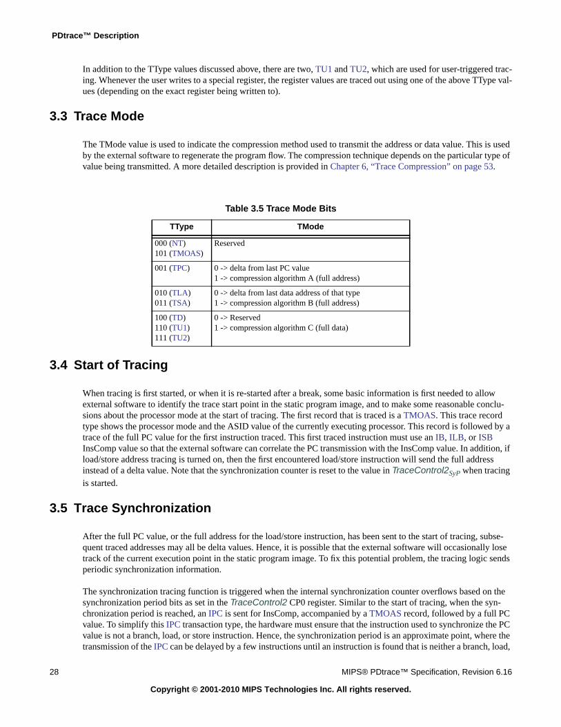
PDtrace™ Description
In addition to the TType values discussed above, there are two, TU1 and TU2, which are used for user-triggered trac-ing. Whenever the user writes to a special register, the register values are traced out using one of the above TType val-ues (depending on the exact register being written to).
3.3 Trace Mode
The TMode value is used to indicate the compression method used to transmit the address or data value. This is usedby the external software to regenerate the program flow. The compression technique depends on the particular type ofvalue being transmitted. A more detailed description is provided in Chapter 6, “Trace Compression” on page 53.
3.4 Start of Tracing
When tracing is first started, or when it is re-started after a break, some basic information is first needed to allowexternal software to identify the trace start point in the static program image, and to make some reasonable conclu-sions about the processor mode at the start of tracing. The first record that is traced is a TMOAS. This trace recordtype shows the processor mode and the ASID value of the currently executing processor. This record is followed by atrace of the full PC value for the first instruction traced. This first traced instruction must use an IB, ILB, or ISBInsComp value so that the external software can correlate the PC transmission with the InsComp value. In addition, ifload/store address tracing is turned on, then the first encountered load/store instruction will send the full addressinstead of a delta value. Note that the synchronization counter is reset to the value in TraceControl2SyP when tracingis started.
3.5 Trace Synchronization
After the full PC value, or the full address for the load/store instruction, has been sent to the start of tracing, subse-quent traced addresses may all be delta values. Hence, it is possible that the external software will occasionally losetrack of the current execution point in the static program image. To fix this potential problem, the tracing logic sendsperiodic synchronization information.
The synchronization tracing function is triggered when the internal synchronization counter overflows based on thesynchronization period bits as set in the TraceControl2 CP0 register. Similar to the start of tracing, when the syn-chronization period is reached, an IPC is sent for InsComp, accompanied by a TMOAS record, followed by a full PCvalue. To simplify this IPC transaction type, the hardware must ensure that the instruction used to synchronize the PCvalue is not a branch, load, or store instruction. Hence, the synchronization period is an approximate point, where thetransmission of the IPC can be delayed by a few instructions until an instruction is found that is neither a branch, load,
Table 3.5 Trace Mode Bits
TType TMode
000 (NT)101 (TMOAS)
Reserved
001 (TPC) 0 -> delta from last PC value1 -> compression algorithm A (full address)
010 (TLA)011 (TSA)
0 -> delta from last data address of that type1 -> compression algorithm B (full address)
100 (TD)110 (TU1)111 (TU2)
0 -> Reserved1 -> compression algorithm C (full data)
28 MIPS® PDtrace™ Specification, Revision 6.16
Copyright © 2001-2010 MIPS Technologies Inc. All rights reserved.

3.6 Trace Overflow and Restart
or a store instruction. Note that the TMOAS associated with synchronization is sent only when the IPC instructionhas been identified, to prevent other TType records between the TMOAS and the full PC trace for the synchroniza-tion. At this juncture, if load/store addresses are not being traced, then this completes all the transmissions needed forsynchronization. If load/store addresses are being traced, then the first load and store instructions encountered afterthe IPC transmission trace a full address value, rather than a delta. This completes the synchronization process. Notethat the synchronization counter is reset to the value in TraceControl2SyP after the IPC has been sent.
Note that the TMOAS record that is traced for synchronization uses a value of 1 for the SYNC bit field (see Figure3.3). This is an aid used by external software to synchronize the InsComp stream and the data stream. To use this bitto synchronize, external software will look in the trace buffer for the first IPC entry; when it finds one, it starts look-ing in the trace buffer from the current cycle onwards for the first TMOAS record with the SYNC bit set to one. Thefirst PC value following this TMOAS record will be a full PC transmission that corresponds to the IPC entry.
The TMOAS record also traces the number of outstanding loads and stores if data value tracing is underway. Thisensures that in an out-of-order data return processor, the software using the record as a synchronization will knowhow many data values are still anticipated and count them correctly. See Figure 3.3.
3.6 Trace Overflow and Restart
In a real implementation, an internal FIFO or buffers may be used to hold address and data values waiting to be com-pressed, formatted, and traced out of the processor. It is possible to have a program sequence that overflows one ormore of these FIFOs. When the FIFO overflows, the core is essentially losing trace data, and hence the outputbecomes illogical and is no longer a true representation of the program execution sequence. In this situation, the mostnatural thing for the core logic to do is abandon tracing in the current cycle, discard all entries in the FIFO, and restarttracing from the next completed instruction in the following cycle. Note that in this situation, the first new instructionto be traced after the overflow must have its full PC value, so this should be treated as an IB, ILB, or ISB. Similar to atrace start or re-start situation, a TMOAS record is first sent after the overflow, and before the full PC value is trans-mitted.
It should be possible for the entire program trace to be captured under all circumstances, and no trace records lost.This is done using the InhibitOverflow control bit from the program or the user’s debugger. When asserted, this bitimplies that the processor core must back-pressure the pipeline and stall it without overflowing the FIFO. (Hence, ifInhibitOverflow is asserted, the core must ensure that Overflow is never asserted.) The pipeline is restarted as soon asthe FIFO starts emptying again.
3.7 Data Order Signal
The data order bits DataOrder are used to indicate the out-of-orderness of load and store data that is traced out. Themain purpose of this is to allow load and store data to be traced out as and when it becomes available, and not main-tain local storage that sequences it. This works by indicating the position of the traced load/store data in the list ofcurrent outstanding loads/stores starting at the oldest. For example, assume that the program issues 5 loads A, B, C,D, E, respectively.
Table 3.6 Load Order Example
Load Cycle # Cache OpLoad DataAvailable
Data TracedOut DataOrder
A 1 Miss - - -
B 2 Hit B B 1 (second oldest)
C 3 Hit C C 1 (second oldest)
MIPS® PDtrace™ Specification, Revision 6.16 29
Copyright © 2001-2010 MIPS Technologies Inc. All rights reserved.

PDtrace™ Description
Table 3.6 shows an example of how these five loads may be traced. Load data that hits in the first-level cache is usu-ally available at some fixed delay from instruction issue. So without loss of generality, we assume in the table thatload data is available in the same cycle as the issued instruction. The number of bits used to specify the DataOrder isprocessor implementation-specific and depends on the number of possible outstanding loads and stores in that imple-mentation. It is assumed that the default number for an implementation of a moderately complex processor is 4 bits,and thus all the examples below use this value.
If the number of outstanding data supported by four bits is exceeded, the processor simply issues the overflow signal,clears its internal buffers, and restarts tracing. If the InhibitOverflow signal is asserted, before continuing the proces-sor must stall until at least some of the outstanding loads/stores are satisfied. Note that if data values are being traced,limits are being reached on other resources like the internal FIFO, and thus it is unlikely that the number-of-outstand-ing-data limit will be so easily reached.
Some processors will graduate a store instruction while still waiting for the store data to become available. Thus aload can bypass a store, and thus load data will be available before a preceding store’s store data is available. Anexample is illustrated in Figure 3.4.
D 4 Miss - - -
E 5 Hit E E 2 (third oldest)
- k - A A 0 (oldest)
- k+p - D D 0 (oldest)
Table 3.7 Data Order with Four Bits
Value Description
0000 data from oldest load/store instruction (is in-order)
0001 data from second-oldest load/store instruction
0010 data from third-oldest load/store instruction
0011 data from fourth-oldest load/store instruction
0100 data from fifth-oldest load/store instruction
0101 data from sixth-oldest load/store instruction
0110 data from seventh-oldest load/store instruction
0111 data from eighth-oldest load/store instruction
1000 data from ninth-oldest load/store instruction
1001 data from tenth-oldest load/store instruction
1010 data from eleventh-oldest load/store instruction
1011 data from twelfth-oldest load/store instruction
1100 data from thirteenth-oldest load/store instruction
1101 data from fourteenth-oldest load/store instruction
1110 data from fifteenth-oldest load/store instruction
1111 data from sixteenth-oldest load/store instruction
Table 3.6 Load Order Example (Continued)
Load Cycle # Cache OpLoad DataAvailable
Data TracedOut DataOrder
30 MIPS® PDtrace™ Specification, Revision 6.16
Copyright © 2001-2010 MIPS Technologies Inc. All rights reserved.

3.7 Data Order Signal
Figure 3.4 An Example of Load Data Bypassing an Earlier Store
Block (1) in Figure 3.4 shows a small program fragment and the sequence of InsComp and TType traces. This proces-sor will graduate and trace all instructions including the first store ISa. This store then waits for the data in r1 before itactually completes its execution. Some processors will order store data. Hence the second store ISb will wait for ISabefore it can complete. But the following loads, ILc and ILd would complete without any delay. In this situation, theTType column of block (1) shows the sequence of data availability. But if the processor must trace data sequentially,then it is required to trace out data in-order as shown in the left column of block (2). This sequential requirement canbe avoided by using the DataOrder bits used to order both the loads and stores. The DataOrder values for the data isshown in the right column of block (2).
Another example that illustrates the combined load/store ordering is shown in Figure 3.8. This table shows in columnone a sequence of only the loads and stores from a program fragment. The second column shows the sequence inwhich the data associated with the loads and stores become available, and the third column shows the DataOrder sig-nal that is needed to trace out the sequence as available.
(1)
Cycle Program InsComp TType Comments
m+0 DIV r3, r2 I NT multi-cycle instr
m+1 MFHI r1 I NT
m+2 SW r1, 0(r3) ISa TSAa data not available
m+3 SW r4, 0(r7) ISb TSAb data not available
m+4 LW r4, 0(r6) ILc TDb store data
m+5 LW r5, 4(r6) ILd TLAc cache hit
m+6 TDc load data
m+7 TLAd cache hit
m+8 TDd load data
m+9+k TDa store data
(2)
Required Data Order DataOrder
TDa 1
TDb 1
TDc 1
TDd 0
Table 3.8 Data (Load/Store) Order Example
Load/Store Data Trace Order DataOrder
Load-A - -
Load-B - -
Store-C - -
Load-D - -
Store-E - -
MIPS® PDtrace™ Specification, Revision 6.16 31
Copyright © 2001-2010 MIPS Technologies Inc. All rights reserved.

PDtrace™ Description
3.8 Tracing During Processor Mode Changes
Note that during normal execution, the processor will change its operation mode frequently. For example, when exe-cuting user-level code, an interrupt may cause the processor to jump to kernel mode to service the interrupt. When theinterrupt has been serviced, the processor will switch back to user mode. A mode change is indicated in the tracinglogic by tracing out a TMOAS for TType.
In the situation that the mode change affects tracing, for example, the tracing system has been set up to trace only inuser mode and not in kernel mode, then the interrupt service routine should not be traced. Upon jumping to kernelmode, the core tracing logic will add a TMOAS as the last record. In the meantime, all the accompanying InsCompvalues are traced as NI (No Instruction) until the TMOAS entry is traced. Once the TMOAS record has been output,nothing new is traced until execution jumps back into user mode. Note that pending information about outstandingloads and stores that were executed before the mode switch could still be traced. By knowing the static instructionstream in the user program, and using the TMOAS record, the external trace reconstruction software can figure outthat tracing was suspended when the processor jumped to kernel mode.
When jumping from a non-tracing mode to a tracing mode, the first record output is TMOAS to indicate the modechange. This is followed by a full PC value of the first instruction in the tracing mode. This will enable the externaltrace reconstruction software to resynchronize itself and track program execution in the desired mode.
When tracing is turned on and the processor enters Debug Mode where tracing is turned off, in the cycle-accuratetracing situation where every cycle is recorded including the ones where no instruction is executed, it is recommendedthat the processor turn off tracing as soon as it is detected that the DM bit is set. Otherwise, since it might take hun-dreds of cycles to fetch the first debug mode instruction through the TAP/probe and execute it, the trace buffer will fillwith records of idle cycles before the execution of the first debug instruction can be used to detect that tracing must beturned off. Thus, recording the entry into Debug mode as a processor mode change and then immediately stopping alltracing will prevent useful trace information in the trace buffer from being overwritten. In this situation, in the pres-ence of MIPS MT, it is recommended that all DM bits (in each VPE) be checked, and when any one of them is set,tracing be immediately stopped when in cycle accurate mode).
Store-F - -
Store-G - -
Store-H - -
Load-I I 8 (ninth oldest)
- A 0 (oldest)
- C 1 (second oldest)
- E 2 (third oldest)
- F 2 (third oldest)
- G 2 (third oldest)
- H 2 (third oldest)
- B 0 (oldest)
- D 0 (oldest)
Table 3.8 Data (Load/Store) Order Example (Continued)
Load/Store Data Trace Order DataOrder
32 MIPS® PDtrace™ Specification, Revision 6.16
Copyright © 2001-2010 MIPS Technologies Inc. All rights reserved.

3.9 Tracing Store Conditionals
3.9 Tracing Store Conditionals
A store conditional instruction that is part of an LL/SC operation may or may not perform the actual store operation.A store conditional is always traced out as an IS or ISB for the InsComp value. If a store address or data is beingtraced, then this associated information is traced as well. It is the responsibility of software to determine from the con-text of the tracing and the program source whether the store conditional was successful or not. For typical uses of LL/SC pairs where the code executes in a loop until the SC succeeds, it should be easy to determine if the SC succeeded.
3.10 Tracing MIPS16e™ Macro Instructions
In the MIPS16e™ ASE, several single MIPS16e instructions expand to a fixed sequence of multiple 32-bit instruc-tions. These include the SAVE, RESTORE, and ASMACRO instructions. (See the MIPS32® Architecture for Pro-grammers Volume IV-a: The MIPS16e™ Application-Specific Extension to the MIPS32® Architecture, documentnumber MD00076).
When executing a Macro instruction, note that the PC address does not change for the instructions that comprise themacro instruction, and thus the core does not output a PC value until it executes the first instruction outside theMacro. In fact, the core indicates the completion of the Macro instruction by outputting a full PC value for the firstinstruction executed after the macro instruction. This instruction could either have been reached sequentially by fall-ing out of the macro sequence, or by executing a branch instruction from within the macro sequence. This full PCvalue is output using a branch indication, e.g., IB for the InsComp value, even though this instruction is most likelynot a branch target. The external reconstruction software will note the preceding Macro instruction, and hence be ableto handle this situation correctly.
Within the macro sequence, normal tracing is carried out. Note that the macro sequence can include, in addition toarithmetic and logical instructions, load and store instructions, which will be traced in a manner similar to loads/stores that are not in a macro instruction sequence. (Note that any branch instruction inside the Macro sequence canonly branch out of the Macro sequence and not to any location within the sequence, since all instructions within thesequence have the same PC value).
3.11 Tracing MIPS16e™ Extend Instructions
A MIPS16e extend instruction is considered a single instruction, and therefore the PC of the extend part is traced.Note that a branch to a MIPS16e extend instruction is to the extend part of the instruction. (For details, refer to theMIPS32® Architecture for Programmers Volume IV-a: The MIPS16e™ Application-Specific Extension to theMIPS32® Architecture, document number MD00076).
3.12 Tracing Instruction Cache and Data Cache Misses
With revision 4.0 of the specification, the PDtrace interface adds the feature in which misses in the instruction cacheand data cache are traced out by the Trace Control Block. This information is associated with the InsComp signal forinstruction caches misses. The instruction cache miss and the data cache miss indicate a miss in the first level of thecache hierarchy. If instruction cache miss tracing is enabled, and PC tracing is disabled, the full PC of the instructionthat missed in the cache must be traced.
Implementation Notes: In a processor that implements an instruction fetch buffer and does speculative executionand instruction prefetching, the instruction cache miss information may be duplicated for all instructions in a cacheline, or the instruction cache miss could have been hidden from the back-end of the execution pipeline due toprefetching. And since tracing is done when an instruction graduates, at the back-end of the pipeline, the instructioncache miss statistics are not guaranteed to be 100% accurate. This problem is made worse in the presence of MIPS
MIPS® PDtrace™ Specification, Revision 6.16 33
Copyright © 2001-2010 MIPS Technologies Inc. All rights reserved.

PDtrace™ Description
MT, where due to frequently switching execution between thread contexts, cache miss information for a specificinstruction of a specific thread context can be lost by the time that instruction is traced out.
Similarly, in an implementation it is possible that not all load/store misses are traced due to certain constraints in howthe pipeline timeline is implemented, or not all operations shown as misses might actually have been a miss. Forexample, in the MIPS32 24KE pipeline, a store operation that misses in the microTLB will show up as a hit in theoutput trace, whether or not this store actually missed in the cache. This is due to the fact that the store operationpasses beyond the trace point in the pipeline before the cache miss or hit logic is done.
3.13 Tracing Potential Function Call/Return Instructions
To debug a program and understand its behavior, it is often sufficient to understand the execution call graph. Whentrace memory is limited, this can be an effective means for program debug for error or performance. To facilitate thisfeature, revision 4.0 of the PDtrace specification adds the ability for the processor to trace a potential function callinstruction or a function return instruction.
Note that the conditional procedure call instructions BGEZAL, BGEZALL, BLTZAL, and BLTZALL are intention-ally omitted from this list. Since executing these instructions does not automatically imply a procedure call, onewould have to examine the PC trace to be certain whether or not a procedure call was invoked. When the TFCR bit isset and PC Tracing is enabled, the FCR bit should be set in the trace format used for the function call/return instruc-tion. When PC Tracing is disabled, in addition to the FCR bit being set for the function call/return instruction, the fullPC of the function call/return instruction must be traced.
3.14 Tracing with MIPS® MT ASE
When the MT ASE is present on the processor, for effective program debug and analysis, trace data needs to be qual-ified with the VPE and the TC number of the instruction being traced. The user via the debugger can request that onlyinstructions from a particular VPE or TC be traced. The analogous function in the CP0 trace control register is pro-vided via the TCNum and CPUId bits.
On the trace output, if MT is present on the processor, then every instruction traced is qualified with the TC identifi-cation. Software can tell from the TCid which VPE it belongs to by reading the appropriate MT CP0 registers. EachPC, address, and data delta computation is done on a per-TC basis. The processor is therefore expected to maintainper-TC delta values. The first time that a PC is traced for a thread, the full address is traced. This initiates the processwhereby future instructions from that thread are done using delta PC values.
To clarify further, each thread of instruction trace is independent and thus must carry its own output of the TMOASrecord, i.e., whenever trace is initiated for a new thread, a TMOAS is required for that thread. This is because eachthread can have its own processor mode such as MIPS32 or MIPS16e, and this needs to be indicated correctly for thatthread. In other words, every time trace is re-started for a thread, perhaps because of a FIFO overflow, a separateTMOAS is required on a per thread basis. A sync operation also requires a TMOAS on a per TC basis. If tracing isinitiated for only a single TC, then only a single TMOAS is required. But if tracing is initiated for multiple TCs or per
Table 3.9 Possible Instructions for Function Call/Returns
ISA Function Call Instructions Function Return Instructions
MIPS32 JAL, JALR, JALR.HB, JALX JR, JR.HB, ERET, DERET
MIPS64 JAL, JALR, JALR.HB JR, JR.HB, ERET, DERET
MIPS16e JAL, JALR, JALRC, JALX JR, JRC
34 MIPS® PDtrace™ Specification, Revision 6.16
Copyright © 2001-2010 MIPS Technologies Inc. All rights reserved.

3.15 Tracing in WAIT State
VPE, then separate TMOAS records are required per TC as described above. Also note that when multiple TCs arebeing traced, and a TMOAS is sent for the first TC after a sync, the sync counter is restarted, even though all TMOASfor other TCs have not yet been sent. Note that TMOAS is also sent on a TC restart, that is, a write to the TC restartregister.
3.15 Tracing in WAIT State
A processor enters a WAIT or sleep state when transitioning to a low-power mode. In this situation, since the proces-sor is not executing any instructions or doing any useful work, it is not necessary to continue tracing, which can be anunnecessary drain on power.
3.16 Trace Trigger from EJTAG Hardware Instruction/Data Breakpoints
The MIPS EJTAG Specification describes the hardware data and instruction breakpoint feature. In brief, a core orprocessor can optionally implement up to 15 instruction and up to 15 data EJTAG hardware breakpoints. These break-points, when encountered during program execution, cause the processor to take a debug exception. Important to thisdiscussion is that a bit (TE bit 2) in the breakpoint control register, when set, allows a trigger signal to be generated(instead of, or in addition to, causing a debug exception). The PC/Data tracing interface uses this trigger signal to trig-ger trace on/off and to enable other tracing modes. When a trigger is generated, this information is traced into thetrace memory so the trace software can have knowledge of when trace triggers were generated.
Please refer to Chapter 9, “EJTAG Trace Registers” on page 94 for the description of the registers which control tracetriggering through EJTAG breakpoints.
3.17 Tracing Performance Counter Values
Dumping performance counter values through the trace stream provides the ability to correlate performance counterevents to the specific instruction execution path. In fact, this provides is a non-intrusive read out of the performancecounter values that does not alter execution behavior. In addition, with the right mechanisms in place, it can allow theability to dynamically change the granularity of reading out the counter values without requiring recompilation ofuser code. For example, if a particular type of stall is suspected to be high in a particular function, that function can betraced individually, and the performance counter set to detect those stalls and dumped out periodically, thereby allow-ing a better correlation of that stall type to particular code blocks within that function to narrow down the perfor-mance bottleneck.
The performance counter trace feature has been defined in specification revision 06.00 and higher. The PeC bit (bit 8in TraceControl3 and bit 0 in TCBControlE) defines whether or not this optional feature is implemented. Anotherbit, PeCE (bit 9 in TraceControl3 and bit 1 in TCBControlE), indicates during program execution whether or notthe feature is enabled. As before, the bit in the TCB register is used by external probe-based debugging and trace con-trol, and the bit in TraceControl3 is used when software-controlled tracing is in effect. Four other bits (bits 9, 10, 11,and 12 in the TraceControl3 register and bits 2, 3, 4, and 5 in TCBControlE register) are used to enable the specificevents that can trigger a dump of the performance counter values. These four events are:
1. Synchronization counter expiration trigger (PeCSync)
2. Hardware trace breakpoint trigger (PeCBP)
3. Function call, function return, or exception occurrence trigger (PeCFCR)
4. When any active performance counter in the processor overflows (PeCOvf)
MIPS® PDtrace™ Specification, Revision 6.16 35
Copyright © 2001-2010 MIPS Technologies Inc. All rights reserved.

PDtrace™ Description
Bit 15 PCTD (Performance Counter Trace Disable) in the Performance Counter Control register is used to providemore detailed control over whether or not a particular performance counter value should be dumped with all the oth-ers. This bit is used to disable the specified performance counter from being traced when performance counter trace isenabled and a performance counter trace event is triggered. Note that the reset and default value for this bit is 0, whichenables tracing of this performance counter. Software must explicitly set this bit to 1 to disable tracing this countervalue.
The number of performance counters is implementation-specific. Implementations may choose to include an addi-tional cycle counter to help calculate event frequencies. This optional cycle counter has these properties:
1. It is not visible in the normal Coprocessor 0 register space, instead its output is only visible in PerformanceCounter trace information.
2. Is 32-bits in width, up-counting from 0x0000000 to 0xFFFFFFFF.
3. Increments at an implementation-specific rate, though the preferred rate is the CPU pipeline clock fre-quency.
4. Roll-overs the count from 0xFFFFFFFF to 0x00000000 without any type of overflow indication.
5. The counter increments only after the PeCE bit is set and at least one of the Performance Counter is traced.The counter does not increment when either the Performance Counter feature is disabled (PeCE bit is clear)or none of the Performance Counters are being traced (all of the PCTD bits are set).
6. Anytime a trigger event causes a Performance Counter value to be deposited into the trace and at least one ofthe Performance Counters is traced (at least one of the PCTD bits is clear), the value of the cycle counter isalso deposited into the trace. The value of the cycle counter is deposited into the trace immediately after thePerformance Counter values.
7. If none of the Performance Counters are traced (all of the PCTD bits are set), the cycle counter value is notdeposited into the trace.
It is not required to have a reset value for this counter, though if the counter is initialized by reset, a reset value of0x00000000 is preferred. It is also implementation specific if the counter is reset upon the clearing of the PeCE bit.
3.18 Filtered Data Trace Mode
This mode is added in PDtrace Specification revision 06.00 and higher. Bit 0 in TraceControl3 (FDT bit) is used toeither disable (value 0) or enable (value 1) this mode. When this mode is enabled, data load and store addresses arecompared to the hardware data breakpoint address, if the addresses match, the data value associated with that matchalong with the address are traced out.
This mode works even when data address and/or value tracing is turned on. However, the general usage model iswhen both PC and Data trace are turned off since it may not always be possible to identify data that was traced due toa match vs. the regular data stream. This mode is used to shadow one or more static (fixed-address) variables. Whenthere is a store to the variable, the store value is captured into the trace. Since there are generally two or more datatriggers/watchpoints, the trace will need to uniquely identify the shadowed variable by also tracing out the associatedaddress.
A main use of this filtered data trace is to support tracing of events in an application code on a Linux system. Thistype of instrumented code tracing is primarily used for performance analysis although it can also be used for event
36 MIPS® PDtrace™ Specification, Revision 6.16
Copyright © 2001-2010 MIPS Technologies Inc. All rights reserved.

3.19 Trace Enabling/Disabling Condition
logging and debug. (This mode has been introduced to provide a mechanism to do low-overhead event tracing fromuser application code, since the User Trace Data registers require a kernel call from user mode.)
Another potential use of this mechanism is to set a watchpoint and track values written to an I/O or peripheral register.Off-chip trace probes can timestamp these values, thus providing valuable performance information on the deltabetween writes, assuming this was the intended use.
3.19 Trace Enabling/Disabling Condition
The input control values to the core that enable tracing can be from the TCB registers or from the CP0 control regis-ters. In addition, trace can also be triggered on and off by the EJTAG hardware instruction and data breakpoint set-tings, as described in 3.16 “Trace Trigger from EJTAG Hardware Instruction/Data Breakpoints” on page 35. Theequations specified here clarify the conditions under which different input factors will enable or disable tracing.
Trace enabling and disabling from software is similar to the hardware method, with the exception that the bits in thecontrol register are used instead of the input enables from registers in the TCB. The TraceControl TS bit controlswhether hardware (via the TCB), or software (via theTraceControl register) controls tracing functionality.
In any given cycle n, an instruction is traced if the following equation evaluates true:
TraceOn & (TriggerOn(n) | MatchEnable | TriggerEnable | DQEnable | FilterDataTraceActive) (EQ 1)
In every cycle, the following state variable is set and then used in the next cycle:
TriggerOn(n+1) <- TraceOn & (TriggerEnable | (TriggerOn(n) & (~TriggerDisable)) (EQ 2)
The various expressions used in (EQ 1) and (EQ 2) are defined here.
TraceOn ← ((TraceControlTS & TraceControlOn) | ((~TraceControlTS) & TCBCONTROLAOn))
MatchEnable ←(TraceControlTS & MTEnableR & (TraceControlG | (( (TraceControlASID ^ EntryHiASID) & (~TraceControlASID_M)) =0 )) & ((TraceControlU & UserMode) | (TraceControlK & KernelMode) | (TraceControlS & SupervisorMode) | (TraceControlE & ExceptionMode) | (TraceControlD & DebugMode))) |((not TraceControlTS) & MTEnable & (TCBCONTROLAG or (TCBCONTROLAASID = EntryHiASID)) & ((TCBCONTROLAU & UserMode) | (TCBCONTROLAK & KernelMode) | (TCBCONTROLAS & SupervisorMode) | (TCBCONTROLAE & ExceptionMode) | (TCBCONTROLAD & DebugMode)))
MTEnableR ← (MT ASE not present) | ((MT ASE present) & ((!TCV) |
(TCV & TCNum=current_TC_context) | (!VPEV) |
(VPEV & VPENum=current_VPE)))
MIPS® PDtrace™ Specification, Revision 6.16 37
Copyright © 2001-2010 MIPS Technologies Inc. All rights reserved.

PDtrace™ Description
MTEnable ← (MT ASE not present) | ((MT ASE present) & ((!TCBCONTROLCTCValid) |
(TCBCONTROLCTCnum & TCNum=current_TC_context) | (!TCBCONTROLCCPUValid) |
(TCBCONTROLCCPUValid & VPENum=current_VPE)))
TriggerEnable ← Lowest Numbered Trigger turns on tracing either because the DBPC orIBPC value was 001, 011, 101, or 111
TriggerDisable ← Lowest Numbered Trigger turns off tracing because the DBPC or IBPCvalue was 000 or 100
FilterDataTraceActive ← TraceControl3FDT &(Load_Address_Matches_Hardware_Breakpoint_Address |
Store_AddresS_Matches_Hardware_Breakpoint_Address)
As seen in the (EQ 1), trace can be turned on only if the master switch On or PDI_TraceOn is first asserted (TraceOn).Once asserted, there are three ways in which instruction tracing can occur:
1. A trigger had occurred in the past that turned on tracing, but no trace disabling trigger had occurred since then(TriggerOn(n)).
2. The input enable signals from the TCB or the trace control register indicate a tracing condition (MatchEnable).This type of tracing is done over general program areas. For example, all of user-level code for a particular pro-cess (ASID specified), or some such conditions.
3. The third method to turn on tracing is from the processor side using the EJTAG hardware breakpoint triggers(TriggerEnable). If EJTAG is implemented, and hardware breakpoints can be set, then using this method, finegrain tracing control is possible. It is possible to send a trigger signal that turns on tracing at a particular instruc-tion. For example, it would be possible to trace a single procedure in a program by triggering on trace at the firstinstruction, and triggering off trace at the last instruction.
Trace is turned off when (EQ 1) evaluates false. Note that tracing can be unilaterally turned off by de-asserting the Onbit or the PDI_TraceOn signal.
38 MIPS® PDtrace™ Specification, Revision 6.16
Copyright © 2001-2010 MIPS Technologies Inc. All rights reserved.

Chapter 4
PDtrace™ Output Trace Formats
One of the two main functions of the TCB is to capture trace information and send it to an on-chip or off-chip tracememory. This trace information is then analyzed by the trace reconstruction software in the debugger. Since tracingthe entire run of a program can require a lot of storage, compression of trace information is a desirable goal. While thetrace information undergoes one level of compression in the core, further compression is possible before the traceinformation is stored to trace memory by the TCB. The TCB achieves this compression using a number of trace for-mats, which eliminate the storage of unnecessary trace bits in each cycle. This chapter describes these formats.
In PDtrace revision 05.00 and higher, a mechanism is added to decouple load/store cache miss indications from datatracing. This is done by augmenting existing trace formats with load/store hit/miss information (see Section 4.3.2.1).The load/store miss indication information is always sent at a fixed offset from the INSCOMP message for that par-ticular instruction. The offset is implementation-dependent (2 for the MIPS 34K core family). Since the offset isalways fixed, we do not need a mechanism at startup to identify the offset.
In PDtrace revision 06.00 and higher, a new feature is added for complex cores like the MIPS 74K core family to pro-vide the user with information about why no instructions completed in a particular cycle. Existing trace formats areexpanded to include this information. The extensions to the trace formats are described in Appendix A,“Implementation-Specific PDtrace™ Enhancements for MIPS32® 74K™ Cores”.
4.1 Single-Pipe Tracing Formats
The formats discussed in this section are relevant only when the core or processor being traced is a single-issue, i.e.,single pipeline implementation. The multi-pipeline case is discussed in 4.3 “Multi-Pipe Tracing Formats”.
4.1.1 Trace Format 1 (TF1)
A processor stall is identified when InsComp[2:0] is 000, TType[2:0] is 000, and no overflow occurs. When the pro-cessor is stalled, no execution trace information needs to be recorded except that this was a stall cycle. This can bedone efficiently using a single bit “1” for this format. This is Trace Format 1 (TF1) as show in Figure 4.1. Note thatthis stall information is needed only when tracing is used to account for all execution cycles, i.e., cycle-accurate trac-ing (TCBCONTROLBCA = 1, see 8.2 “TCBCONTROLB Register”). However, TF1 generation is suppressed if theprocessor executes a WAIT instruction. Once the processor exits the WAIT state, TF1 messages resume.
Note that when parsing a trace format sequence, if the first bit of the trace format is a one, then this is TF1 and thenext bit is the first bit of the next trace format.
Figure 4.1 TF1 (Trace Format 1)
0
1
MIPS® PDtrace™ Specification, Revision 6.16 39
Copyright © 2001-2010 MIPS Technologies Inc. All rights reserved.

PDtrace™ Output Trace Formats
4.1.2 Trace Format 2 (TF2)
A study of program traces shows that with only PC tracing enabled, nothing of significance needs to be captured alarge percentage of the time. For instance, when TType[2:0] is NT (000), i.e., No data Trace, there is nothing to betraced. So, when TType[2:0] is NT and InhibitOverflow is 0, the only significant trace output is InsComp[2:0].Having used a single bit value of “1” for TF1, we indicate the combination of non-zero InsComp[2:0], zeroTType[2:0], and zero overflow in two bits (102). The next three bits of the format are the value of InsComp[2:0].This trace format with five bits is called Trace Format 2 (TF2), as shown in Figure 4.2.
Figure 4.2 TF2 (Trace Format 2 Single-Pipe)
Revision 4.00 (and higher) of the PDtrace specification introduces the ability to trace instruction fetch misses and totag an instruction that might be a function call or return. These are fundamental properties that could impact mostinstructions in the stream that are represented by a non-zero InsComp value. Therefore, TF2 can optionally be aug-mented by two bits to trace out this information. These bits are optional and only traced when specifically requestedby the user via bit TLSIF (bit 11) in TCBCONTROLB register. Hence, for correct interpretation of the trace formats,the trace reconstruction software must be told whether or not these 2 bits are present in each relevant trace format.This impacts other formats well, and will be discussed in each sub-section separately. The two optional bits of theTF2 format are shown in Figure 4.3.
• The Im bit indicates the Instruction miss for this instruction in the instruction cache.
• The optional Fcr bit indicates that this instruction is potentially a function call or return instruction.
Figure 4.3 TF2 with Optional Bits (Trace Format 2 Single-Pipe)
4.1.3 Trace Format 3 (TF3)
When TType[2:0] is not NT (000) and there is no overflow, all trace information needs to be captured. This is theTF3 format shown in Figure 4.4. The DataOrder[2:0] value is an exception in that it only needs to be captured on thelast cycle of a Data Trace (DT for the TType[2:0] value). Hence, a slight distinction is made between this format TF3(which excludes the LoadOrder[2:0] value, see Figure 4.4), and the format TF4 (which includes the DataOrder[2:0]value, see Figure 4.7). This shows a data order value of 4 bits, but this is implementation-dependent and the numberof bits in the DataOrder field is preset by the implementation in the TCBCONTROLCNumDO bits. The total length ofthe format increases by the corresponding number of bits.
TF3 is distinguished from TF2 by having 0002 on the first three bits. TF3 may be either 27 or 43 bits wide, dependingon whether 16 or 32 bits is specified by the TCBCONTROLAADW field. (See 8.1 “TCBCONTROLA Register”).
When cycle-by-cycle accuracy is not needed, the least-significant bit of TF3 may be removed by the TCB hardware.Please refer to Section 5.1.1 on page 50.
4 2 1 0
InsComp 1 0
6 5 4 2 1 0
ImFcr
InsComp 1 0
40 MIPS® PDtrace™ Specification, Revision 6.16
Copyright © 2001-2010 MIPS Technologies Inc. All rights reserved.

4.1 Single-Pipe Tracing Formats
Figure 4.4 TF3 (Trace Format 3 Single-Pipe)
Revision 4.00 (and higher) of the PDtrace specification introduces the ability to trace instruction fetch misses and totag an instruction that might be a function call or return. These are fundamental properties that could impact mostinstructions in the stream that are represented by a non-zero InsComp value. Therefore, TF3 can optionally be aug-mented by two bits to trace out this information. These bits are optional and only traced when specifically requestedby the user. Hence, the trace reconstruction software must be told whether these bits are present. This impacts otherformats well, and will be discussed in each sub-section separately. The two optional bits of the TF3 format are shownin Figure 4.5.
Figure 4.5 TF3 with Optional Bits (Trace Format 3 Single-Pipe)
Revision 6.00 (and higher) of the PDtrace specification introduces the ability to trace performance counter values. Ifthis feature is enabled by the user, this information is traced through TF3, which can be optionally augmented by onebit. This expanded version of the TF3 format is show in Figure 4.6. If the PCV bit is set to zero, reconstruction soft-ware must interpret the trace format as before. If the PCV bit is set to one, reconstruction software must interpret theAD bits of the format as the value of the performance counter. In addition, the TType must be set to DT, and TEndmust be set to zero.
Figure 4.6 TF3 with Optional Performance Counter and other bits (Trace Format 3 Single-Pipe)
4.1.4 Trace Format 4 (TF4)
The TF4 format is shown in Figure 4.7. TF4 covers the case when TType[2:0] is set to DT and TEnd is set to 1, thatis, the last cycle of the current data trace. This is shown in Figure 4.7, where the pattern on bits [9:6] distinguishesTF4 from TF3. Bits [8:6] are equal to 0012 for a Type[2:0] value of DT and bit 9 has a value of 1 for TEnd.
Note that the TF4 format will be used for the last cycle of both Load and Store Data transmission, a small ineffi-ciency.
26(42) 11 10 9 8 6 5 3 2 1 0
AD TMode TEnd TType InsComp 0 0 0
(44)
28 27 26 11 10 9 8 6 5 3 2 1 0
Im Fcr AD TMode TEnd TType InsComp 0 0 0
(45)
29 28 27 26 11 10 9 8 6 5 3 2 1 0
PCV Im Fcr AD TMode TEnd TType InsComp 0 0 0
MIPS® PDtrace™ Specification, Revision 6.16 41
Copyright © 2001-2010 MIPS Technologies Inc. All rights reserved.

PDtrace™ Output Trace Formats
Figure 4.7 TF4 (Trace Format 4 Single-Pipe)
Revision 4.00 (and higher) of the PDtrace specification introduces the ability to trace instruction fetch misses, load/store data misses, and to tag an instruction that might be a function call or return. Therefore, TF4 can optionally beaugmented by three bits to trace out this information. These bits are optional and only traced when specificallyrequested by the user. Hence, the trace reconstruction software must be told if these 3 bits are present. The optionalbits of the TF4 format are shown in Figure 4.8. For non-coherent MIPS cores, only this format includes the LSm bit,that is, the bit that indicates a possible load/store data cache miss. This is because a data miss is associated with thetransmitted data rather than the instruction that caused the miss.
Figure 4.8 TF4 with Optional Bits (Trace Format 4 Single-Pipe)
4.1.5 Trace Format 5 (TF5)
When an overflow happens all other trace values are undefined and hence all current cycle trace values can be dis-carded. (When an overflow does occur, the trace always sends a full PC value in the next cycle. This is used forresynchronizing to the execution path.) The Trace Format 5 (TF5) shown in Figure 4.9 indicates an overflow.
Revision 4.00 of the PDtrace specification added one bit to this format for a total of 5 bits in preparation for futureadditional features. Those expected features proved to be unnecessary and for that reason Revision 6.13 (and higher)reverts the length of this format back to 4 bits.
Figure 4.9 TF5 (Trace Format 5)
4.1.6 Trace Format 6 (TF6)
Trace Format 6 (TF6) shown in Table 4.10 is provided to the TCB to transmit information that does not directly orig-inate from the cycle by cycle trace data. That is TF6 can be used by the TCB to store any information it wants in thetrace memory, within the constraints of the specified format. This information can then be used by software for anypurpose. For example, TF6 can be used to indicate a special condition, trigger, semaphore, breakpoint, or break intracing that is encountered by the TCB.
30(46) 15 14 11 10 9 8 7 6 5 3 2 1 0
AD DataOrder TMode 1 1 0 0 InsComp 0 0 0
(49)
33 32 31 30 15 14 11 10 9 8 7 6 5 3 2 1 0
LSm
ImFcr
AD DataOrder TMode 1 1 0 0 InsComp 0 0 0
4 3 2 1 0
1 1 0 0
42 MIPS® PDtrace™ Specification, Revision 6.16
Copyright © 2001-2010 MIPS Technologies Inc. All rights reserved.

4.1 Single-Pipe Tracing Formats
Figure 4.10 TF6 (Trace Format 6)
The definition of TCBcode and TCBinfo is shown in Table 4.1.
Revision 4.00 (and higher) of the PDtrace specification uses two of the TCBcode fields to indicate that Instruction orData Hardware Breakpoints were caused by the instruction in the trace format immediately preceding this TF6 for-mat. Whether the trigger caused by the breakpoint turned trace off or on is indicated by the appropriate TCBinfo fieldvalue. Note that if the processor is tracing and trace is turned off, this would be passed on to the external trace mem-ory appropriately. If the processor is not tracing, and trace is turned on by a hardware breakpoint, then this recordwould show up in trace memory as the first instruction to be traced (it is also the one that triggered trace on). If tracingis on-going and other triggers continue to keep turning on trace, then this would show up as a TF6 in trace memory.Revision 5.00 (and higher) of the PDtrace specification define an additional bit in TCBInfo, when TCBcode ‘1001’ isused (see Table 4.1).
Table 4.1 TCBcode and TCBinfo fields of Trace Format 6 (TF6)
TCBcode Description TCBinfo
0000 Trigger Start: Identifies start-point of trace. TCBinfo identifies what caused the trigger. Cause of trigger.Taken from the Triggercontrol register gener-ating this trigger.
0100 Trigger End: Identifies end-point of trace. TCBinfo identifies what caused the trigger.
1000 Reserved. This value used to indicate a trigger center. Starting from PDtrace rev 6.00, thisvalue is reserved for future use.
1100 Trigger Info: Information-point in trace. TCBinfo identifies what caused the trigger.
00011 No trace cycles: Number of cycles where the processor is not sending trace data, but a stall isnot requested by the TCB. This can happen when the processor, during its execution, switchesmodes internally that take it from a trace output required region to one where trace output wasnot requested.For example, if it was required to trace in User-mode but not in Kernel-mode, then when theprocessor jumps to Kernel-mode from User-mode, and an internal FIFO is emptied, then theprocessor stops sending trace information. In order to maintain an accurate account of totalexecution cycles, the number of such no-trace cycles have to be tracked and counted. ThisTCBcode does this tracking.
Number of cycles (Allzeros is equal to 256).If more than 256 isneeded, the TF6 formatis repeated.
01011 Back stall cycles: Number of cycles when no trace information was sent, for whatever rea-son.
1001 Instruction or Data Hardware Breakpoint Trigger: Indicates that one or more of the instruc-tion or data breakpoints were signalled and caused a trace trigger. Bit 8 of the TCBinfo fieldindicates whether it was an instruction (0) or data (1) breakpoint that caused the trigger. Bit 9indicates whether or not trace was turned off (0) or on (1) by this trigger. Bits 13:10 encodesthe hardware breakpoint number. Bit 14 indicates if tracing from the coherence manager wasaffected (1) or not (0).When tracing is turned off, a TF6 will be the last format that appears in the trace memory forthat tracing sequence. The next trace record should be another TF6 that indicated a trigger onsignal.It is important to note that a trigger that turns on tracing when tracing is already on will notnecessarily get traced out, and is optional depending on whether or not there is a free slotavailable during tracing. Similarly, when tracing is turned off, then a trigger that turns offtracing will not necessarily appear in trace memory. Finally, if multiple breakpoints causetrigger actions, only one of the matching breakpoints is encoded in bits 13:10, and the triggeraction is reported in bit 9.
Values are asdescribed.
15 8 7 4 3 2 1 0
TCBinfo TCBcode 0 1 0 0
MIPS® PDtrace™ Specification, Revision 6.16 43
Copyright © 2001-2010 MIPS Technologies Inc. All rights reserved.

PDtrace™ Output Trace Formats
4.2 Format Enhancements for the MT ASE
In the presence of hardware-based multi-threading such as that provided by the MT ASE, there needs to be a methodto indicate the thread ID (or TC, thread context) for every traced instruction. This is possible in one of two ways:
1. The first method would typically be used when the multithreading method is coarse-grained or block-based, thatis, instructions from a single thread are executed for a while before switching to another thread. In this type ofscheme, it would suffice to trace out the thread ID every time it changes and continue tracing instructions untilthere is a context switch. At which point, the new thread ID is traced, and so on. The thread ID thus traced is doneusing trace format 7 (TF7) illustrated in this section.
2. The second method is used when instructions from multiple threads are interleaved with a finer granularity. Inthis situation, the thread ID might change every cycle, or in the case of a scheme like SMT (SImultaneous multi-threading), different instructions issued every cycle might belong to different thread contexts. In this situation,the thread ID must be traced with every traced instruction. This might add significantly to the amount of tracedata, but there is no avoiding this extra burden. In this situation, every trace format discussed thus far, with theexception of TF1, TF5, and TF7, will be prefixed with a number of bits needed for the thread context value.
Bits in the TCB control register MTtrace determine which method is chosen, as well as the option to not trace thethread ID in a processor implementing the MT ASE.
4.2.1 Trace Format 7 (TF7)
Trace Format 7 (TF7) shown in Table 4.11 is provided to the TCB to transmit information about the current ThreadID and is only used by a processor that implements the MT ASE. This format is used to indicate that the formatsbeing sent following this one all belong to the indicated Thread ID. Note that this is a sub-format of TF6. with a TCB-code value of 1110 and with the TCid value in the TCBinfo field.
Figure 4.11 TF7 (Trace Format 7)
1101 Reserved for future use Undefined
0010, 01101010
1110 Used for processors implementing MIPS MT ASE, see format TF7 TC value
xx11 TCB implementation dependent Implementation depen-dent
1. TF6 formats with this TCBcode is not transmitted when TCBCONTROLBCA is 0
Table 4.1 TCBcode and TCBinfo fields of Trace Format 6 (TF6) (Continued)
TCBcode Description TCBinfo
15 8 7 4 3 2 1 0
TCTCBcode
11100 1 0 0
44 MIPS® PDtrace™ Specification, Revision 6.16
Copyright © 2001-2010 MIPS Technologies Inc. All rights reserved.

4.3 Multi-Pipe Tracing Formats
4.2.2 TF2--TF4 Augmented for MT ASE
Up to 8 bits for the TC value is prepended to formats TF2, TF3, and TF4. The figure below illustrates the example ofpre-pending 4 bits to format TF2 to support a hypothetical 34K core. Three bits in the TCB control register TCbitsindicate how many TCid bits are needed for a particular core. In this example, the TCbit value would be set to four.
Figure 4.12 TF2 with Optional Bits and TCid Bits (Trace Format 2 Single-Pipe)
4.3 Multi-Pipe Tracing Formats
A processor with multiple pipelines requires additional support for sending trace information to trace memory. TheTCB can perform some combining and the kind of format crunching as shown in the single-pipe case to reduce thenumber of bits that are sent out each cycle. If there are k pipelines within the core, 1, 2,... k, then for each cycle, theTCB generates a trace format from each pipeline, in that respective order. The external software programmer mustrefer to the User’s Guide for that core to determine the order of the pipelines as hooked up to the PDtrace™ interface.
The trace format TF1 is usable by the TCB without change for multi-pipe tracing. The TF1 format indicates that thespecific pipe did not complete an instruction and had no data to send.
TF5 is a common format. That is, all the pipes have to flush the trace buffer when just one of them has overflowed.Hence, a single instance of TF5 will suffice to cover all the 1..k pipeline stages. The trace reconstruction softwaremust take this into account as it parses the trace formats in trace memory.
The TF6 format is also usable by the TCB without change, and as a common format. A TF6 format can be used afterall the formats for the respective pipelines have been sent. Note that if needed, pipeline-specific information can beencoded within the TF6 format bits.
4.3.1 Multi-Pipe Trace Format 2-4 (TF2, TF3, TF4)
The TF2, TF3, and TF4 formats need the additional PgmOrder[2:0] value for multi-pipeline tracing. The PgmOrderfield is added to all of them, right after the InsComp field, as shown in Figure 4.13, Figure 4.14, and Figure 4.15. ThePgmOrder field is 3 bits wide to allow up to 8 pipelines. The number of processor pipelines is specified in theTCBCONFIGPiN field. See 8.7 “TCBCONFIG Register (Reg 0)” on page 82.
Figure 4.13 TF2 (Trace Format 2 Multi-Pipe)
10 7 6 5 4 2 1 0
TCid ImFcr
InsComp 1 0
7 5 4 2 1 0
PgmOrder InsComp 1 0
MIPS® PDtrace™ Specification, Revision 6.16 45
Copyright © 2001-2010 MIPS Technologies Inc. All rights reserved.

PDtrace™ Output Trace Formats
Figure 4.14 TF3 (Trace Format 3 Multi-Pipe)
TF4 for multi-pipe trace is defined as was the case for single-pipe trace. In the example in Figure 4.15, the TEnd bit(bit 12) is set, and the TType field (bits 8:6) is set to DT (1002).
Figure 4.15 TF4 (Trace Format 4 Multi-Pipe)
4.3.2 Trace Format Extensions for Coherent Systems
The PDtrace architecture requires the coherent synchronization Id to be traced out from each core in a coherent sys-tem to allow correlation between requests from a core with transactions at the CM. The exact implementation of howthis information is made available is highly dependent on the particular core on which it is implemented. We describeone mechanism that is implemented in the 34K core for CMP and extends every existing trace format by between 1and 4 bits in Section 4.3.2.1.
4.3.2.1 Expanding Existing Trace Formats
The first mechanism expands trace formats TF2,TF3,and TF4. Each of these formats is expanded by one to four bits.Each instruction that is capable of generating a bus request (“LSU” instruction) adds at least two bits. All non-LSUinstructions add a single bit (0) to the end of the trace formats. An LSU instruction that hits in the cache adds two bitsa “10”. If the instruction misses in the cache, it adds four bits - 11XY, where XY represent the COSId. The hit/miss/COSId information for an LSU instruction is always sent after the instruction completion message for that instructionhas been sent. Specifically, it is always attached to the second LSU instruction after the original instruction. For the34K, this guarantees that the hit/miss information is available at the time it needs to be sent out. Note: An implemen-tation may choose to treat the LSm bit in a TF4 packet as a ‘don’t care’. Reconstruction software must not rely on theaccuracy of this value to get a data cache hit/miss indication.
29(45) 14 13 12 11 9 8 6 5 3 2 1 0
ADTMod
eTEnd PgmOrder TType InsComp 0 0 0
32(48) 17 16 14 13 12 11 9 8 7 6 5 3 2 1 0
AD LoadOrderTMod
e1 PgmOrder 1 0 0 InsComp 0 0 0
46 MIPS® PDtrace™ Specification, Revision 6.16
Copyright © 2001-2010 MIPS Technologies Inc. All rights reserved.

Chapter 5
TCB Trace Word
Following the compression of data into the Trace Formats described in Chapter 4, “PDtrace™ Output Trace Formats”on page 39, the trace information must be streamed to either on-chip or off-chip dedicated trace memory. As previ-ously explained, each of the major Trace Formats is a different size. In order to ensure the efficient storage of thisinformation in a fixed-width on-chip memory and the transmission of this data through a fixed-width interface to off-chip memory, the Trace Formats are first gathered into Trace Words of regular width. This section describes the for-mat of these Trace Words.
5.1 Trace Word
A Trace Word (TW) is defined to be 64 bits wide. A TW has a 4-bit type indicator on bits [3:0], an optional 2 or 4 bitsto indicate the origin or source of this trace word, and regular TFs stacked up in the remaining 58 or 56 respective bitsof the word. Figure 5.1, Figure 5.2, and Figure 5.3 show the 64-bit wide TW. The source bits are valuable and used inan environment where trace data from multiple cores or different sources needs to be combined and written into a sin-gle trace memory. The trace regeneration software can then use these bits to sort out which trace words belong towhich core or other traced logic in the chip or SOC.
It is recommended to allow the number of source bits be a configuration option for a core. The value thus chosen iswritten to the two-bit TWSrcWidth field in the TCB Control register (Figure 8.2 on page 72). For non-zero sourceoptions, the value of source to be used is preset to 0 during configuration in the TWSrcVal field in the TCB Controlregister. This value can be overwritten by software if needed and changed from the default value of zero.
Note that in all Trace Word examples illustrated later in this chapter, it is assumed that the source field is zero. Butthose examples could have been constructed in a similar manner for source field widths of 2 and 4 bits without anyloss of generality.
Figure 5.1 Trace Word with Zero Source Bits
Figure 5.2 Trace Word with Two Source Bits
63 4 3 0
Trace Type
63 6 5 4 3 0
Trace Source Type
MIPS® PDtrace™ Specification, Revision 6.16 47
Copyright © 2001-2010 MIPS Technologies Inc. All rights reserved.

TCB Trace Word
Figure 5.3 Trace Word with Four Source Bits
The Trace portion of a TW consists of one or more Trace Formats, TF1 through TF6. Note that trace formats TF1,TF2, TF5, and TF6 have a fixed size, while TF3 and TF4 can vary in size. The sizes of formats TF3 and TF4 arebased on the value of the ADW bits. A further optimization is possible with an address value; that is, the redundantsign bits (in the upper address bits) can be optionally chopped from the formats, especially if the format straddles twoTWs. This happens when TType is set to TPC, TLA, or TSA, TEnd is set to 1, and TMode is set to 0.
When Type is set to the TMOAS processor mode, this is traced as a TF3 with the TMOAS information in the ADfield of that trace format type.
A TW is built by adding the TFs back to back until all 60 bits of the Trace field are used. If the last TF does not fit inTrace, it spills to the first bits of the Trace field in the next TW. The Type indicator is used to indicate where the firstnew TF starts in the new Trace field, which indirectly indicates the number of bits used to complete the TF from theprevious TW.
When a TF cannot be completed in the remaining bits of a TWn, it is sometimes more efficient to discard those bits ofthe TWn and simply repeat all of them in the following TWn+1. This is indicated in TWn+1 by setting Type to 1.When Type is 1, the first new TF of a TW starts at bit 0 in the Trace field. Since the previous TWn ended with anuncompleted TF, a Type of 1 in TWn+1 instructs the decode software to discard the uncompleted TF in TWn. Table5.1 describes the word types for the TW.
Table 5.1 Trace Word Type Field Descriptions
Decimalvalue of theType field
The first newTF starts at
this bit in theTrace field Description
0 N/A This TW does not carry any trace information. The Trace field is set to all zeroes.In the off-chip interface, the Trace field can be truncated to make the TW fit the bit-width of theoff-chip interface.For on-chip trace, this TW is not stored in memory.
1 0 This indicates a situation where a new TF is started at the beginning of this TW. This can happenwhen: (1) a new trace is begun, (2) the TF in the previous TW was completed, and (3) an incom-plete TF at the end of the previous TW is discarded.If the last trace format of the previous TW was a TF3 with TType set to TPC, TLA or TSA, TEndset to 1, TMode set to 0, and with at least one AD bit, that is considered to be a completed TF for-mat, and no bits are discarded from the previous TW.
2 - 14 (Type - 1) * 4 The partial TF from the previous TW is completed in this TW in the bits available before the firstnew TF, i.e., bits 0..((Type -1)*4)-1) in the Trace field.If extra bits are available after completing the straddling TF, the rest of the bits until the first newTF start are undefined.TF3 formats sending the last part of a relative address are allowed to remove the AD bits to onlyshow the needed sign bits. This enables compression of sign-extended address or data bits whenthe TF3 straddles a TW.
63 8 7 4 3 0
Trace Source Type
48 MIPS® PDtrace™ Specification, Revision 6.16
Copyright © 2001-2010 MIPS Technologies Inc. All rights reserved.

5.1 Trace Word
As an example of how a TW is built, consider the trace sequence shown in Table 5.2. In this example, the ADW valueis assumed to be 16 bits wide (a zero value for TCBCONTROLAADW).
The TF sequence in Table 5.2 will create the set of TWs shown in Figure 5.4. The shaded boxes containing a “u” areunused bits. Shaded boxes with an “s” indicate redundant sign-bits from a TF3 format; these sign-bits could not beremoved by compression, and must be included as part of the AD field. A “1” indicates the single bit of 1 in a TF1format.
Figure 5.4 Trace Word from Example Trace in Table 5.2
15 56 If an implementation does not support any TFs longer than 56 bits and does not utilize a 4-bitsource field, type 15 can be used to indicate that the first new TF begins at bit 56. In such an imple-mentation, a TF can always be completed within 2 TWs, and the continuation field below is notneeded.
No new TF The TF started in the previous TW could not be completed within 52 bits1. It might complete inthis TW, but if it does not complete, then the next TW will have a Type value higher than one.
1. 52 bits is the maximum allowable bits used to complete a TF from a previous TWn-1, if a new one is to start in TWn. This is so
because a Type value of 14 indicates the maximum bit position (bit 52) in the Trace field, where a new TF will start.
Table 5.2 Example Trace Sequence
Cycle # Trace Format Cycle # Trace Format
1 TF3 (16 significant AD bits) 2 TF3 (16 significant AD bits)
3 TF2 4 TF1
5 TF1 6 TF1
7 TF1 8 TF2
9 TF2 10 TF1
12 TF2 11 TF2
13 TF2 14 TF1
15 TF3 (5 significant AD bits) 16 TF1
17 TF2 18 TF2
19 TF2 20 TF2
21 TF3 (11 significant AD bits) 22 TF1
23 TF3 (6 significant AD bits) 24 TF6 (Stop indicator)
Trace Type
5 5 5 4 4 4 3 3 2 2 2 1 1
TW 9 6 2 8 4 0 6 2 8 4 0 6 2 8 4 0 3 0
1 1 TF2 TF3 TF3 12 TF2 1 s s s s s s s s s s s TF3 1 TF2 TF2 TF2 1 TF2 TF2 1 1 1 13 TF3 1 s s s s s TF3 TF2 TF2 TF2 u TF2 24 u u u u u u u u u u u u u u u u u u u u u u u u u u u u u u u u u u u u u u u TF6 (stop) TF3 2
Table 5.1 Trace Word Type Field Descriptions (Continued)
Decimalvalue of theType field
The first newTF starts at
this bit in theTrace field Description
MIPS® PDtrace™ Specification, Revision 6.16 49
Copyright © 2001-2010 MIPS Technologies Inc. All rights reserved.

TCB Trace Word
In the example in Figure 5.4, the TF3 straddling TW3/TW4 have had insignificant sign bits cut from the full TF3 for-mat. It is optional for TCB hardware to do this extra compression of TF3 formats, but TW decode software mustalways be designed to handle this extra compression.
5.1.1 Cycle Inaccurate Trace
The TF1 format is needed only when a sequence of the trace must show cycle-by-cycle behavior of the processorwithout missing any cycles. When the trace regeneration software only needs to show the sequence of instructionsexecuted, the TF1 format which shows processor stall cycles can be omitted. In this latter situation, an additionaloptimization removes bit zero on the other TFs before storing to trace memory. The example trace sequence in Table5.2 will then produce the TWs shown in Figure 5.5. Note that to reconstruct the trace accurately, external softwaremust know what type of tracing was enabled at the TCB.
Figure 5.5 Trace Word from Example Trace in Table 5.2 (No TF1 trace)
In the example shown in Figure 5.5, the TF3 straddling TW2/TW3 has had insignificant sign bits removed from thefull TF3 format. It is optional for TCB hardware to make this extra compression of TF3 format, but TW decode soft-ware must be able to handle this.
Additionally when not tracing for cycle accurate information, the TF6 formats TCBcode 0001 and 0101 are omittedfrom the Trace Words (not shown in Figure 5.4 and Figure 5.5). Cycle accurate versus cycle inaccurate tracing in con-trolled by the TCBCONTROLBCA bit.
5.1.1.1 Trace Word collection.
Figure 5.6 shows how the TCB builds Trace Words using the Trace Formats cycle-by-cycle, using the trace informa-tion. Trace Words from Figure 5.4 are used.
Figure 5.6 Cycle-by-cycle Trace Word from Example Trace in Table 5.2
Trace Type
5 5 5 4 4 4 3 3 2 2 2 1 1
TW 9 6 2 8 4 0 6 2 8 4 0 6 2 8 4 0 3 0
1 TF2 TF2 TF3 TF3 12 TF3 TF2 TF2 TF2 TF2 s s s s s s s s s s s TF3 TF2 TF2 TF2 TF2 13 TF6 (stop) s s s s s s s s s s TF3 s TF3 64 u u u u u u u u u u u u u u u u u u u u u u u u u u u u u u u u u u u u u u u u u u u u u u u u u u u u u u u u u u TF6 2
Trace Type
5 5 5 4 4 4 3 3 2 2 2 1 1
Cycle TW 9 6 2 8 4 0 6 2 8 4 0 6 2 8 4 0 3 0
1
1
free TF3 12 free TF3 TF3 13 f TF2 TF3 TF3 14 1 TF2 TF3 TF3 1
50 MIPS® PDtrace™ Specification, Revision 6.16
Copyright © 2001-2010 MIPS Technologies Inc. All rights reserved.

5.2 End of Trace Indication
5.2 End of Trace Indication
In the examples in the previous section, the Trigger TF6 (stop: TCBcode == 0100) was used to indicate an End Trig-ger, and this also implied an end to the tracing. This stop trigger deasserts TCBCONTROLBEN, and the TCB flushesout the current TW. However, the TCBCONTROLBEN bit can be deasserted for other reasons, and this trace end mustbe indicated externally using a different mechanism to distinguish it from the end-trigger case. The recommendedmethod to accomplish this is to allow the TCB to fill the unused bits in the last TW with zeroes. Note that nine bits ofconsecutive zeroes in the Trace field will be identified as a TF3 with no information; that is, InsComp and TType areboth zero. Ordinarily this will never be generated by the Trace Format generator, and can therefore be used as a end-of-trace indicator.
If less than nine bits remain in the last TW, an incomplete TF is detected by trace software. After that, no additionalTWs are generated by the TCB. This should not be a problem for trace-regenerating software, as this is just like anyother arbitrary cut in the trace stream.
5.3 On-chip Trace Memory Format
The on-chip trace memory is defined to be a 64-bit wide memory. The TWs defined in 5.1 “Trace Word”, are storedin consecutive address locations. The trace memory is only written when a full TW is available, and thus a new TWmight not be written each cycle, since a new TW might not be created each cycle.
The memory image will exactly match the TW sequence shown in Figure 5.4 or Figure 5.5, depending on whetherTF1 formats are included.
5
2
free 1 16 free 1 1 17 free 1 1 1 18 free TF2 1 1 1 19 free TF2 TF2 1 1 1 110 free 1 TF2 TF2 1 1 1 111 free TF2 1 TF2 TF2 1 1 1 112 free TF2 TF2 1 TF2 TF2 1 1 1 113 free TF2 TF2 TF2 1 TF2 TF2 1 1 1 114 free 1 TF2 TF2 TF2 1 TF2 TF2 1 1 1 115 free s s s s s s s s s s s TF3 1 TF2 TF2 TF2 1 TF2 TF2 1 1 1 116 free 1 s s s s s s s s s s s TF3 1 TF2 TF2 TF2 1 TF2 TF2 1 1 1 1
17
TF2 1 s s s s s s s s s s s TF3 1 TF2 TF2 TF2 1 TF2 TF2 1 1 1 1
3
free u TF2 218 free TF2 u TF2 219 free TF2 TF2 u TF2 220 free TF2 TF2 TF2 u TF2 221 free s s s s s TF3 TF2 TF2 TF2 u TF2 222 free 1 s s s s s TF3 TF2 TF2 TF2 u TF2 2
23
TF3 1 s s s s s TF3 TF2 TF2 TF2 u TF2 2
4
free TF3 224 u u u u u u u u u u u u u u u u u u u u u u u u u u u u u u u u u u u u u u u TF6 (stop) TF3 2
Trace Type
5 5 5 4 4 4 3 3 2 2 2 1 1
Cycle TW 9 6 2 8 4 0 6 2 8 4 0 6 2 8 4 0 3 0
MIPS® PDtrace™ Specification, Revision 6.16 51
Copyright © 2001-2010 MIPS Technologies Inc. All rights reserved.

TCB Trace Word
5.4 Probe Trace Word Transmission
The Probe interface can support a TR_DATA bus width of 4, 8, or 16 bits. When a TW is ready to be sent, it is put onthe TC_Data pins to the PIB. The PIB will feed the TW through on the available TR_DATA pins, starting withTC_Data[n:0] on the TR_DATA[n:0] utilized pins. Depending on the value of n, this will take 16, 8, or 4 transmissions.If a clock multiplier is used in the PIB, then 2, 4, 8, or 16 transmissions can be completed in one core clock cycle.
As long as no new TW is available for transmission, the TC_Data bus will show all zeros, allowing the PIB to keeptransmitting this on the TR_DATA bits to also show all zeros.
On an 8-pin TR_DATA trace interface, running at core-clock frequency, the trace from the TW’s in Figure 5.6 will lookas shown in Figure 5.7 on the Probe IF. This assumes sufficient buffering to hold the TWs in the TCB when theybecome available for transmission, and a latency of one clock before the first part of an available TW on the TC_databus appears on the TR_DATA pins.
Figure 5.7 Cycle-by-Cycle TR_DATA (8-bit) of Example Trace in Table 5.2
The probe sampling the TR_DATA pins should look for a non-zero transmission. When that occurs, the following bitsup to a collective count of 64-bits (i.e., including the first non-zero 4/8/16-bit value) will form a TW. After 64 bits, theprobe should begin looking for a new non-zero transmission. A non-zero transmission can start at any time after a fullTW is received.
Cycle TR_DATA[7:0] Cycle TR_DATA[7:0] Cycle TR_DATA[7:0] Cycle TR_DATA[7:0]
1 zero 11 TW1[55:48] 21 TW2[31:24] 31 TW3[47:40]
2 zero 12 TW1[63:56] 22 TW2[39:32] 32 TW3[55:48]
3 zero 13 zero 23 TW2[47:40] 33 TW3[63:56]
4 zero 14 zero 24 TW2[55:48] 34 TW4[7:0]
5 TW1[7:0] 15 zero 25 TW2[63:56] 35 TW4[15:8]
6 TW1[15:8] 16 zero 26 TW3[7:0] 36 TW4[23:16]
7 TW1[23:16] 17 zero 27 TW3[15:8] 37 zero
8 TW1[31:24] 18 TW2[7:0] 28 TW3[23:16] 38 zero
9 TW1[39:32] 19 TW2[15:8] 29 TW3[31:24] 39 zero
10 TW1[47:40] 20 TW2[23:16] 30 TW3[39:32] 40 zero
52 MIPS® PDtrace™ Specification, Revision 6.16
Copyright © 2001-2010 MIPS Technologies Inc. All rights reserved.

Chapter 6
Trace Compression
This chapter describes compression techniques that can be used when tracing different values. The methods used arequite different for each “type" of value. For example, the PC may be sent as a delta from the previous PC address. Atother times, the full PC value needs to be sent when the trace process starts at the beginning of tracing, or after abuffer overflow, or for synchronization; in this case, the PC can be sent un-compressed, or some method such as bit-block compression can be used. The sections below discuss these various techniques as they correspond to the TModebit value in the Trace Word. Note that the single-bit TMode bit allows two ways in which to send the informationbeing currently traced.
6.1 PC Tracing
When TMode is zero, it implies that the delta of the PC value is transmitted. This delta is computed from the PC valueof the instruction executed just before the branch target instruction (e.g., the instruction executed in the branch delayslot after a branch instruction). The computed delta is then right-shifted by one bit, since this bit is never used. Notethat the value can be negative or positive, thus is a signed 16-bit value, and the upper bits need to be sign-extendedbefore transmission.
PC_delta = (new_PC - last_PC) >> 1 (EQ 1)
If the width of the computed delta value is bigger than the width of the data field (ADW), the lower bits are sent first,followed by the upper bits.
When the TMode value is one, it implies that the full PC value is transmitted. Depending on the width of the bus, thismay take multiple cycles. Again, the first cycle transmits the least significant bits, and so on.
6.2 Load or Store Address Tracing
With a TMode value pf zero, the load address transmitted is a delta from the last transmitted load address. Stores aresimilar, where the computed delta is from the last transmitted store address. Note that the last load instruction can bea load instruction of any type, i.e., LB, LW, etc., and the same is true for stores.
load_address_delta = current_load_address - last_load_address (EQ 2)
store_address_delta = current_store_address - last_store_address (EQ 3)
Note that the delta transmission is quite effective when the load or store addresses are increasing or decreasingsequentially.
With a TMode value of one, the value transmitted is the full address of either the load or the store. Depending on thewidth of the trace bus and the processor data width, this could require multiple cycles to transmit.
MIPS® PDtrace™ Specification, Revision 6.16 53
Copyright © 2001-2010 MIPS Technologies Inc. All rights reserved.

Trace Compression
6.3 Load and Store Data Tracing
Though data values are less prone to good compression techniques, delta values and bit-block compression tech-niques might be useful in achieving some compression ratio. This revision of the PDtrace specification does not dic-tate any compression for data values. The TMode value of zero is reserved for a future compression scheme, and theTMode value of one is used to transmit the full data value.
6.4 Using Early TEnd Assertion
This technique was discussed in Table F.1. When tracing data address or value, the tracing logic can optionally makea decision to cut off the trailing sign bits of the data and assert TEnd early, before all the bits of the address or datahave been traced. For example, redundant sign bits need not be transmitted for accurate reconstruction of the data.Note that this data compression technique can be applied to any value traced in the AD field in the trace formats, be itPC address, load/store address, or load/store data. Also note that this technique is optional, but the software must becapable of handling this situation for implementations with PDtrace Specification 03.00 and higher.
54 MIPS® PDtrace™ Specification, Revision 6.16
Copyright © 2001-2010 MIPS Technologies Inc. All rights reserved.

6.4 Using Early TEnd Assertion
MIPS® PDtrace™ Specification, Revision 6.16 55
Copyright © 2001-2010 MIPS Technologies Inc. All rights reserved.

Chapter 7
PDtrace™ Control Using CP0 Registers
PDtrace permits users to control both the type and amount of trace data produced, within predetermined constraints,in order to minimize the trace bandwidth to the useful set. Trace data output can be controlled by software, using CPOregisters, or by the debug probe, using registers in the Trace Control Block (TCB). This chapter describes softwarecontrol; debug probe control is described in Chapter 8, “Trace Control Block (TCB) Registers” on page 67.
7.1 Trace Controls Overview
The majority of trace control bits are used to specify the conditions under which tracing is enabled. The list belowbriefly explains the various types of trace controls.
• An overall trace control bit TraceControlOn, controls whether tracing is turned on or off. When this bit is asserted,the control bits that control the per-instruction decision of whether the core should trace or not include bits inTraceControl such as G, ASID, U, S, K, E, and D. These bits are expected to be modified only when the processoris not tracing. That is, if tracing is currently on, then tracing must be turned off, a change made to one of thesebits, and then tracing turned back on. If not done in this way, the ability of the reconstruction software to parsethe trace output obtained from the TCB is not guaranteed.
For processors that implement MIPS MT ASE or in a multi-processor configuration, there are other control bitssuch as TCNum and CPUid that control which thread context, VPE (virtual processing element), or CPU in theconfiguration is currently tracing. The same rule about changing the control bits only when tracing is turned offapplies here with.
• When tracing is turned on, one needs to specify what kind of information is to be traced, i.e., only the PC, or alsothe load/store addresses and data. This is done using the Mode bits in TraceControl2. In addition to this, anotherbit, TraceControlTB specifies that the PC of all taken branches be traced, not only the ones that are staticallyunpredictable. When asserted, this will generate a lot of trace data, since in a RISC architecture such as MIPS,typically every third or fourth instruction is a branch instruction. The main purpose of this all-branches tracing isto enable the TCB to track the execution addresses in the core without referring to the static program image,when needed. This knowledge can be used by the TCB to provide additional filtering of the trace data.
• TraceControlIO (InhibitOverflow) is used to ensure that trace data is never lost because of implementation-spe-cific internal FIFO or buffer overflow. This loss of trace data could result when a large number of bits are tracedeach cycle while the bandwidth out of the core or TCB is far less. If this bit is asserted and an internal FIFO is inimminent danger of overflowing, the core must stall its pipe while the FIFO is emptied.
7.2 Software Trace Control
Just as the TCB hardware can control tracing functionality using the input PDI_ signals, the PDtrace architectureallows software to control tracing with similar enables and with the same flexibility. This is done by setting bits in theCoprocessor 0 TraceControl register to appropriate values. To ensure that only hardware or software can control trac-ing at any given point in time, a trace select bit is used in TraceControl. A processor reset sets the trace select bit to thedefault trace input select from the TCB hardware.
MIPS® PDtrace™ Specification, Revision 6.16 56
Copyright © 2001-2010 MIPS Technologies Inc. All rights reserved.
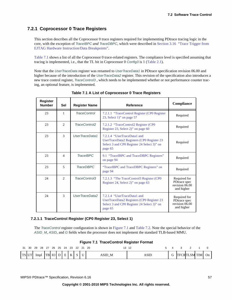
7.2 Software Trace Control
7.2.1 Coprocessor 0 Trace Registers
This section describes all the Coprocessor 0 trace registers required for implementing PDtrace tracing logic in thecore, with the exception of TraceIBPC and TraceDBPC, which were described in Section 3.16 “Trace Trigger fromEJTAG Hardware Instruction/Data Breakpoints”.
Table 7.1 shows a list of all the Coprocessor 0 trace-related registers. The compliance level is specified assuming thattracing is implemented, i.e., that the TL bit in Coprocessor 0 Config3 is 1 (Table 2.1).
Note that the UserTraceData register was renamed to UserTraceData1 in PDtrace specification revision 06.00 andhigher because of the introduction of the UserTraceData2 register. This revision of the specification also introduces anew trace control register, TraceControl3 , which needs to be implemented whether or not performance counter trac-ing, an optional feature, is implemented.
7.2.1.1 TraceControl Register (CP0 Register 23, Select 1)
The TraceControl register configuration is shown in Figure 7.1 and Table 7.2. Note the special behavior of theASID_M, ASID, and G fields when the processor does not implement the standard TLB-based MMU.
Table 7.1 A List of Coprocessor 0 Trace Registers
RegisterNumber Sel Register Name Reference Compliance
23 1 TraceControl 7.2.1.1 “TraceControl Register (CP0 Register23, Select 1)” on page 57
Required
23 2 TraceControl2 7.2.1.2 “TraceControl2 Register (CP0Register 23, Select 2)” on page 60
Required
23 3 UserTraceData1 7.2.1.4 “UserTraceData1 andUserTraceData2 Registers (CP0 Register 23Select 3 and CP0 Register 24 Select 3)” onpage 65
Required
23 4 TraceIBPC 9.1 “TraceIBPC and TraceDBPC Registers”on page 94
Required
23 5 TraceDBPC “TraceIBPC and TraceDBPC Registers” onpage 94
Required
24 2 TraceControl3 7.2.1.3 “The TraceControl3 Register (CP0Register 24, Select 2)” on page 63
Required forPDtrace specrevision 06.00
and higher
24 3 UserTraceData2 7.2.1.4 “UserTraceData1 andUserTraceData2 Registers (CP0 Register 23Select 3 and CP0 Register 24 Select 3)” onpage 65
Required forPDtrace specrevision 06.00
and higher
Figure 7.1 TraceControl Register Format31 30 29 28 27 26 25 24 23 22 21 20 13 12 5 4 3 2 1 0
TS UT Impl TB IO D E K S U ASID_M ASID G TFCRTLSM TIM On
MIPS® PDtrace™ Specification, Revision 6.16 57
Copyright © 2001-2010 MIPS Technologies Inc. All rights reserved.

PDtrace™ Control Using CP0 Registers
Table 7.2 TraceControl Register Field Descriptions
Fields
DescriptionRead/Write
ResetState ComplianceName Bits
TS 31 The trace select bit is used to select between the tracecontrol block and the software trace control bits. A valueof zero selects the trace control block registers, and avalue of one selects the trace control bits in theTraceControl register.
R/W 0 Required
0 30 The previously defined use of this bit to specify usertrace formats (as type 1 or type 2), is deprecated inPDtrace specification revisions 05.00 and higher. Thisfunctionality is now provided by the UserTraceData1 andUserTraceData2 registers.
0 0 Reserved
Impl 29:28 Reserved for implementation-specific use. Refer to thecore-specific implementation document for usagedetails.
Impl-specific
Impl-spe-cific
Reserved firimplementation
TB 27 Trace All Branch. When set to 1, this tells the processorto trace the PC value for all taken branches, instead ofonly those whose branch target address is staticallyunpredictable.
R/W Undefined Required
IO 26 Inhibit Overflow. This bit is used to indicate to the core’strace logic that slow but complete tracing is desired.Hence, the core tracing logic must not allow a FIFOoverflow, which results in discarded trace data. This isachieved by stalling the pipeline when the FIFO is nearlyfull, so that no trace records are lost.
R/W Undefined Required
D 25 When set to one, this enables tracing in Debug Mode(see 2.2 “Processor Modes” on page 16). For trace to beenabled in Debug mode, the On bit must be one, andeither the G bit must be one, or the current processASID must match the ASID field in this register.When set to zero, trace is disabled in Debug Mode,regardless of other bits.
R/W Undefined Required
E 24 When set to one, tracing in Exception Mode (see2.2 “Processor Modes” on page 16) is enabled. For traceto be enabled in Exception mode, the On bit must be one,and either the G bit must be one, or the current processASID must match the ASID field in this register.When set to zero, trace is disabled in Exception Mode,regardless of other bits.
R/W Undefined Required
K 23 When set to one, tracing in Kernel Mode (see2.2 “Processor Modes” on page 16) is enabled. For traceto be enabled in Kernel mode, the On bit must be one,and either the G bit must be one, or the current processASID must match the ASID field in this register.When set to zero, trace is disabled in Kernel Mode,regardless of other bits.
R/W Undefined Required
58 MIPS® PDtrace™ Specification, Revision 6.16
Copyright © 2001-2010 MIPS Technologies Inc. All rights reserved.

7.2 Software Trace Control
S 22 When set to one, tracing in Supervisor Mode (see2.2 “Processor Modes” on page 16) is enabled. For traceto be enabled in Supervisor mode, the On bit must beone, and either the G bit must be one, or the current pro-cess ASID must match the ASID field in this register.When set to zero, trace is disabled in Supervisor Mode,regardless of other bits.If the processor does not implement Supervisor Mode,this bit is ignored on write and returns zero on read.
R/W Undefined Required (ifSupervisor
Mode is imple-mented, is
Reserved other-wise)
U 21 When set to one, tracing in User Mode (see2.2 “Processor Modes” on page 16) is enabled. For traceto be enabled in User mode, the On bit must be one, andeither the G bit must be one, or the current process ASIDmust match the ASID field in this register.When set to zero, trace is disabled in User Mode, regard-less of other bits.
R/W Undefined Required
ASID_M 20:13 Mask value applied to the ASID comparison (when theG bit is zero). A “1” in any bit in this field inhibits thecorresponding ASID bit from participating in the match.As such, a value of zero in this field compares all bits ofASID. Note that the ability to mask the ASID value is notavailable in the hardware register bit; it is only availablevia the software control register.If the processor does not implement the standard TLB-based MMU, this field is ignored on writes and returnszero on reads.
R/W Undefined Required
ASID 12:5 The ASID field to match when the G bit is zero. Whenthe G bit is one, this field is ignored.If the processor does not implement the standard TLB-based MMU, this field is ignored on writes and returnszero on reads.
R/W Undefined Required
G 4 When set, tracing is enabled for all processes, providedthat other enabling bits (U, S, etc.,) are also true.If the processor does not implement the standard TLB-based MMU, this field is ignored on writes and returns 1on reads. This causes all match equations to work cor-rectly in the absence of an ASID.
R/W Undefined Required
TFCR 3 When set, this indicates to the PDtrace interface that theoptional Fcr bit must be traced in the appropriate traceformats. If PC tracing is disabled, the full PC of the func-tion call (or return) instruction must also be traced. Notethat function call/return information is only traced iftracing is actually enabled for the current mode.
R/W Undefined Required
Table 7.2 TraceControl Register Field Descriptions (Continued)
Fields
DescriptionRead/Write
ResetState ComplianceName Bits
MIPS® PDtrace™ Specification, Revision 6.16 59
Copyright © 2001-2010 MIPS Technologies Inc. All rights reserved.

PDtrace™ Control Using CP0 Registers
7.2.1.2 TraceControl2 Register (CP0 Register 23, Select 2)
The TraceControl2 register, described in Figure 7.2 and Table 7.3, provides additional trace control and status infor-mation. Note that some fields in the TraceControl2 register are read-only, but have a reset state of “Undefined”. This isbecause these values are loaded from TCB register bits.
TLSM 2 When set, this indicates to the PDtrace interface thatinformation about data cache misses should be traced. IfPC, load/store address and data tracing are disabled (seethe TraceControl2Mode field), the full PC and load/store
address are traced for data cache misses. If load/storedata tracing is enabled, the LSm bit must be traced in theappropriate trace format. Note that data cache missinformation is only traced if tracing is actually enabledfor the current mode.
R/W Undefined Required
TIM 1 When set, this indicates to the PDtrace interface that theoptional Im bit must be traced in the appropriate traceformats. If PC tracing is disabled, the full PC of theinstruction that missed in the I-cache must be traced.Note that instruction cache miss information is onlytraced if tracing is actually enabled in the current mode.
R/W Undefined Required
On 0 This is the master trace enable switch in software con-trol. When zero, tracing is always disabled. When set toone, tracing is enabled whenever the other enabling bitsare also true.
R/W 0 Required
Figure 7.2 TraceControl2 Register Format31 30 29 28 21 20 19 12 11 7 6 5 4 3 2 0
SyPExtCPUIdV CPUId TCV TCNum Mode
Valid-Modes
TBI TBU SyP
Table 7.2 TraceControl Register Field Descriptions (Continued)
Fields
DescriptionRead/Write
ResetState ComplianceName Bits
60 MIPS® PDtrace™ Specification, Revision 6.16
Copyright © 2001-2010 MIPS Technologies Inc. All rights reserved.

7.2 Software Trace Control
Table 7.3 TraceControl2 Register Field Descriptions
Fields
DescriptionRead /Write
ResetState ComplianceName Bits
SyPExt 31:30 This field is optional for PDtrace revisions 06.00 andhigher and preset to 0 for earlier revisions. This is usedto optionally extend the length of the synchronizationperiod field SyP (bits 2:0) in this register. The value ofSyP is extended by assuming that these two bits are jux-taposed to the left of the three bits of SyP (SyPExt.SyP).When only SyP was used to specify the synchronization
period, the value was 2x, where x was computed fromSyP by adding 5 to the actual value represented by thebits. A similar formula applied to the 5 bits just obtainedby the juxtaposition of SyPExt and SyP. Sync period val-
ues greater than 231 are UNPREDICTABLE. Since thevalue of 11010 represents the value of 31 (with +5), allvalues greater than 11010 are UNPREDICTABLE.
Note that with these new bits, a sync period range of 25
to 231 cycles can now be obtained.
0 or R/W (for
PDtracerevi-sions06.00and
higher)
0 Required forPDtrace rev06.00 and
higher.
CPUIdV 29 Only implemented on a processor with MT or multi-coreSOC. Otherwise, this field must be written as zero andreturns zero on reads. When set, the CPUId field speci-fies the number of the VPE or CPU that must be traced.Otherwise, instructions from all VPEs are traced whenother conditions for tracing are valid. On an MT system,this bit is ignored if TCV is set.
R/W Undefinedfor a multi-VPE MT ormulti-coreprocessor,
0 otherwise
Required if MTASE is imple-mented, other-wise reserved
CPUId 28:21 Only implemented on a processor with MT or multi-coreSOC. Otherwise, this field must be written as zero;returns zero on reads. On an MT core, specifies the num-ber of the VPE to trace when CPUIdV is set. On a multi-core system, this is the Ebase.CPUId value. On an MTsystem, this bit is ignored if TCV is set.
R/W Undefinedfor a multi-VPE MT ormulti-coreprocessor,
0 otherwise
Required if MTASE is imple-mented, other-wise reserved
TCV 20 Only implemented on a processor with MT. Otherwise,this field must be written as zero and returns zero onreads. When set, the TCNum field specifies the numberof the TC that must be traced. Otherwise, instructionsfrom all TCs are traced when other conditions for tracingare valid.
R/W Undefinedfor a MTprocessor,
0 otherwise
Required if MTASE is imple-mented, other-wise reserved
TCNum 19:12 Only implemented on a processor with MT. Otherwise,this field must be written as zero; returns zero on read.Specifies the number of the TC to trace when TCV is set.For any given MT implementation, only the appropriatenumber of bits encoding the TC number are used in theright-most position of this field; the upper bits areignored.
R/W Undefinedfor a MTprocessor,
0 otherwise
Required if MTASE is imple-mented, other-wise reserved
MIPS® PDtrace™ Specification, Revision 6.16 61
Copyright © 2001-2010 MIPS Technologies Inc. All rights reserved.

PDtrace™ Control Using CP0 Registers
Mode 11:7 These 5 bits provide the trace mode values.It is optional for an implementation to allow PC tracingto be turned off. This must be clearly documented by thecore implementation-specific document. When it isoptional, bit 11 is tied to a value of 1 and setting bit 11 to0 is simply ignored by the processor. Reading this bitalways returns a value of one.
R/W Undefined Required
Valid-Modes
6:5 This field specifies the subset of tracing that is supportedby the processor (see 2.3 “Subsetting” on page 17).
R Preset Required
TBI 4 This bit indicates how many trace buffers are imple-mented by the TCB, as follows:
This bit is loaded when the TCBCONTROLBOfC bit is
set.
R Undefined Required
Table 7.3 TraceControl2 Register Field Descriptions (Continued)
Fields
DescriptionRead /Write
ResetState ComplianceName Bits
Bit Trace The Following
0 PC
1 Load address
2 Store address
3 Load data
4 Store data
Encoding Meaning
00 PC tracing only
01 PC and load and store address tracingonly
10 PC, load and store address, and loadand store data
11 Reserved
Encoding Meaning
0 Only one trace buffer is implemented,and the TBU bit of this register indi-cates which trace buffer is imple-mented
1 Both on-chip and off-chip trace buffersare implemented by the TCB, and theTBU bit of this register indicates towhich trace buffer the traces is cur-rently written.
62 MIPS® PDtrace™ Specification, Revision 6.16
Copyright © 2001-2010 MIPS Technologies Inc. All rights reserved.

7.2 Software Trace Control
7.2.1.3 The TraceControl3 Register (CP0 Register 24, Select 2)
The TraceControl3 register, described in Figure 7.3 and Table 7.3, provides additional trace control and status infor-mation. Note that some fields in the TraceControl3 register are read-only, but have a reset state of “Undefined”. This isbecause these values are loaded from TCB register bits.
TBU 3 This bit denotes to which trace buffer the trace is cur-rently being written and is used to select the appropriateinterpretation of the TraceControl2SyP field.
This bit is loaded from the TCBCONTROLBOfC
R Undefined Required
SyP 2:0 The period (in cycles) to which the internal synchroniza-tion counter is reset when tracing is started or when thesynchronization counter has overflowed.
This field is loaded from the TCBCONTROLBSyP bits.
R Undefined Required
Figure 7.3 TraceControl3 Register Format31 16 15 14 13 12 11 10 9 8 7 3 2 1 0
0 0PeCOvf
PeCFCR
PeCBP
PeCSyn
c
PeCE
PeC 0TrI-DLE
TRPAD
FDT
Table 7.3 TraceControl2 Register Field Descriptions (Continued)
Fields
DescriptionRead /Write
ResetState ComplianceName Bits
Encoding Meaning
0 Trace data is being sent to an on-chiptrace buffer
1 Trace Data is being sent to an off-chiptrace buffer
SyP Sync Period
000 25
001 26
010 27
011 28
100 29
101 210
110 211
111 212
MIPS® PDtrace™ Specification, Revision 6.16 63
Copyright © 2001-2010 MIPS Technologies Inc. All rights reserved.

PDtrace™ Control Using CP0 Registers
Table 7.4 TraceControl3 Register Field Descriptions
Fields
DescriptionRead /Write
ResetState ComplianceName Bits
0 31:16 Reserved for future use; Must be written as zero; returnszero on reads.
0 0 Reserved
0 15:14 Reserved for future use; Must be written as zero; returnszero on reads. (Hint to architect: reserved for futureexpansion of performance counter trace events).
0 0 Reserved
PeCOvf 13 Trace performance counters when one of the perfor-mance counters overflows its count value. Enabled whenset to 1.
R/W 0 Required afterrevision 06.00
and higher
PeCFCR 12 Trace performance counters on function call/return or onan entry to an exception handler. Enabled when set to 1.
R/W 0 Required afterrevision 06.00
and higher
PeCBP 11 Trace performance counters on hardware breakpointmatch trigger. Enabled when set to 1.
R/W 0 Required afterrevision 06.00
and higher
PeCSync 10 Trace performance counters on synchronization counterexpiration. Enabled when set to 1.
R/W 0 Required afterrevision 06.00
and higher
PeCE 9 Performance counter tracing enable. When set to 0, trac-ing of performance counter values as specified is dis-abled. To enable, this bit must be set to 1. This bit is usedunder software control. When trace is controlled by anexternal probe, this enabling is done via the TCB controlregister.
R/W 0 Required afterrevision 06.00
and higher
PeC 8 Specifies whether or not Performance Control Tracing isimplemented. This is an optional feature that may beomitted by implementation choice. See 3.17 “TracingPerformance Counter Values” on page 35 for details.
R Preset Required afterrevision 06.00
and higher
0 7:3 Reserved for future use. Must be written as zero; returnszero on reads.
0 0 Required afterrevision 06.00
and higher
TrIDLE 2 Trace Unit Idle. This bit indicates if the trace hardware iscurrently idle (not processing any data). This can be use-ful when switching control of trace from hardware tosoftware and vice versa. The bit is read-only and updatedby hardware.
R 1 Required afterrevision 06.00
and higher
TRPAD 1 Trace RAM access disable bit, disables program soft-ware access to the on-chip trace RAM using load/storeinstructions. This bit is a copy of the TRPAD bit (bit 18)in TCBCONTROLB.
The affected registers are TCBTW*, TCBRDP, TCBWP,TCBSTP. None of these registers are writeable whenTRPAD is set. Reads of TCBTW* return zero with noside-effects when TRPAD is set.
R 0 Required afterrevision 06.00
and higher
64 MIPS® PDtrace™ Specification, Revision 6.16
Copyright © 2001-2010 MIPS Technologies Inc. All rights reserved.

7.2 Software Trace Control
7.2.1.4 UserTraceData1 and UserTraceData2 Registers (CP0 Register 23 Select 3 and CP0 Register 24Select 3)
A software write to any bits in the UserTraceData1 register will trigger a trace record to be written indicating a type 1user format. Similarly, a write by software to any bits in the UserTraceData2 register will trigger a trace record to bewritten indicating a type 2 user format. The UT bit in the TraceControl register was used to dictate the type of tracerecord, but the use of this bit has been deprecated in the PDtrace architecture revisions 06.00 and higher. It is imple-mentation dependent whether or not writes to this register cause dependency stalling, or the latency between writes tothe register and the subsequent generation of the trace record. Please read the core-specific implementation specifica-tion for this information. Please note that since these two registers are in CP0 register space, the access to these regis-ters is ruled by CP0 access restrictions imposed by the system. For example, when a processor is under the control ofan operating system such as Linux, these registers cannot be written by code executing in user-level privilege mode.
FDT 0 Filtered Data Trace Mode enable bit. When the bit is 0,this mode is disabled. When set to 1, this mode isenabled. Reset value is 0. This mode is described inSection 3.18 on page 36
R/W 0 Required afterrevision 06.00
and higher
Figure 7.4 UserTraceData1 and UserTraceData2 Register Format31 32-bit Register 0
63 64-bit Register 0
Table 7.5 UserTraceData1 Register Field Descriptions
Fields
DescriptionRead/Write
ResetState ComplianceName Bits
Data 31:0 or63:0
Software readable/writable data. When written, this trig-gers a user format trace record type1 into the tracestream to be written to the trace memory.
R/W 0 Required
Table 7.6 UserTraceData2 Register Field Descriptions
Fields
DescriptionRead/Write
ResetState ComplianceName Bits
Data 31:0 or63:0
Software readable/writable data. When written, this trig-gers a user format trace record type 2 into the tracestream to be written to trace memory.
R/W 0 Required forPDtrace spec
06.00 andhigher
Table 7.4 TraceControl3 Register Field Descriptions (Continued)
Fields
DescriptionRead /Write
ResetState ComplianceName Bits
MIPS® PDtrace™ Specification, Revision 6.16 65
Copyright © 2001-2010 MIPS Technologies Inc. All rights reserved.
PDtrace™ Control Using CP0 Registers
66 MIPS® PDtrace™ Specification, Revision 6.16
Copyright © 2001-2010 MIPS Technologies Inc. All rights reserved.

Chapter 8
Trace Control Block (TCB) Registers
The TCB uses several registers to control its operation. These registers are accessed via the EJTAG TAP interface.This chapter describes these registers in detail. They are listed in Table 8.1 and Table 8.2.
Table 8.1 Trace Control Block Registers
Register NameEJTAG TAP Controller
Instruction Value Description
TCBCONTROLA 0x10 Control register in the TCB mainly used for controlling the trace input signalsto the core on the PDtrace interface.
TCBCONTROLB 0x11 Control register in the TCB mainly used to specify what to do with the traceinformation. The REG [25:21] field in this register specifies the TCB internalregister to be accessed by the TCBDATA register. A list of all the registers thatcan be accessed by the TCBDATA register is shown in Table 8.2.
TCBDATA 0x12 This register is used to access registers specified by the REG field in theTCBCONTROLB register.
TCBCONTROLC 0x13 Control Register in the TCB used to control and hold tracing information.
TCBCONTROLD 0x15 Added to support tracing on coherent cores such as the MIPS 1004K inPDtrace revision 05.00 and higher.
TCBCONTROLE 0x16 Added for support of new features in PDtrace revision 06.00 and higher. Newfeatures include, for example, performance counter tracing, etc.
Table 8.2 Registers Selected by TCBCONTROLBREG (accessed through TCBDATA)
REG[4:0]RegisterSelected Register Description Compliance
0 TCBCONFIG TCB Configuration register that contains information about the TCB hardware configu-ration.
Required
1-3 Reserved Reserved for future use. Reserved
4 TCBTW Trace Word Read. This register holds the Trace Word just read from on-line trace mem-ory.
Required if on-chip memory
exists.5 TCBRDP Trace Word Read Pointer. Points to the location in the on-line trace memory where thenext Trace Word will be read. A TW read has the side-effect of post-incrementing thisregister value to point to the next TW location. (A maximum value wraps the addressaround to the beginning of the trace memory.)
6 TCBWRP Trace Word Write Pointer. Points to the location in the on-line trace memory where thenext new Trace Word will be written.
7 TCBSTP Trace Word Start Pointer. Pointer into Trace Buffer that is used to determine when allentries in the trace buffer have been filled.
8-15 Reserved Reserved for future use. Reserved
MIPS® PDtrace™ Specification, Revision 6.16 67
Copyright © 2001-2010 MIPS Technologies Inc. All rights reserved.

Trace Control Block (TCB) Registers
8.1 TCBCONTROLA Register
The trace output from the processor on the PDtrace interface can be controlled by the trace input signals to the proces-sor from the TCB. The TCB uses a control register, TCBCONTROLA, whose values are used to change the signal val-ues on the PDtrace input interface. External software (i.e., debugger), can therefore manipulate the trace output bywriting to the TCBCONTROLA register.
The TCBCONTROLA register is written by the EJTAG TAP controller instruction TCBCONTROLA (0x10). See theMIPS EJTAG Specification (MD00047) for more details regarding new TAP instructions. Starting with PDtrace rev6.00, this register is also mapped to offset 0x3000 in drseg. See Section 8.15 “Memory-Mapped Access to PDtrace™Control and On-Chip Trace RAM” on page 91 for information on how this register can be accessed via drseg.
Compliance: This register is required.
The format of the TCBCONTROLA register is shown below, and the fields are described in Table 8.3.
Figure 8.1 TCBCONTROLA Register Format
16-23 TCBTRIGx Trigger Control registers 0-7 are used to specify some conditions that cause the firingof triggers, and to control the resulting action.
Optional
24-31 Reserved Reserved for future use. Reserved
31 30 29 27 26 25 24 23 22 20 19 18 17 16 15 14 13 12 5 4 3 2 1 0
SyPExt Impl 0 VModes ADW SyP TB IO D E S K U ASID GTFCR
TLSM
TIM
On
Table 8.2 Registers Selected by TCBCONTROLBREG (accessed through TCBDATA) (Continued)
REG[4:0]RegisterSelected Register Description Compliance
68 MIPS® PDtrace™ Specification, Revision 6.16
Copyright © 2001-2010 MIPS Technologies Inc. All rights reserved.

8.1 TCBCONTROLA Register
Table 8.3 TCBCONTROLA Register Field Descriptions
Fields
DescriptionRead /Write
ResetState ComplianceName Bits
SyPExt 31:30 These two bits used to be implementation-specific untilPDtrace spec revision 06.00, when it reverts to architectur-ally defined bits to extend the SyP (sync period) field forimplementations that need a higher numbers of cyclesbetween synchronization events.The value of SyP is extended by assuming that these twobits are juxtaposed to the left of the three bits of SyP(SyPExt.SyP). When only SyP was used to specify the
synchronization period, the value was 2x, where x wascomputed from SyP by adding 5 to the actual value repre-sented by the bits. A similar formula is applied to the 5bits just obtained by the juxtaposition of SyPExt and SyP.
Sync period values greater than 231 are UNPREDICT-ABLE. Since the value of 11010 represents the value of 31(with +5), all values greater than 11010 are UNPREDICT-ABLE.
Note that with these new bits, a sync period range of 25 to
231 cycles can now be obtained.
0 or R/W(for specrevisions06.00 and
higher)
0 Required afterPDtrace revi-
sion 06.00 andhigher
Impl 29:27 This field is reserved for implementation-specific use.Refer to the processor specification for the format and def-inition of this field.
Undefined Optional
0 26 Reserved for future use. Must be written as zero; returnszero on read.
0 0 Required
VModes 25:24 This field specifies the type of tracing that is supported bythe processor, as follows:
This field is preset to the TCB register value ValidModes
R Preset Required
ADW 23 The address and data value width used in the trace for-mats.0: The width is 16 bits.1: The width is 32 bits.
R Preset Required
Encoding Meaning
00 PC tracing only
01 PC and load and store address tracingonly
10 PC, load, and store address, and loadand store data.
11 Reserved
MIPS® PDtrace™ Specification, Revision 6.16 69
Copyright © 2001-2010 MIPS Technologies Inc. All rights reserved.

Trace Control Block (TCB) Registers
SyP 22:20 Used to indicate the synchronization period.The period (in cycles) between which the periodic syn-chronization information is to be sent is defined as shownin the table below, when the trace buffer is either on-chipor off-chip (as determined by the TCBCONTROLBOfC bit).
R/W 000 Required
TB 19 Trace All Branches. This signal is used to indicate that thecore must trace either full or incremental PC values for allbranches instead of only the unpredictable ones.
R/W Undefined Required
IO 18 Inhibit Overflow. This signal is used to indicate to the coretrace logic that slow but complete tracing is desired.Hence, the core tracing logic must not allow a FIFO over-flow, which results in discarded trace data. This isachieved by stalling the pipeline when the FIFO is nearlyfull, so that no trace records are lost.
R/W Undefined Required
D 17 When set to one, tracing is enabled in Debug mode, i.e.,when the DM bit is one in the Debug register. For trace tobe enabled in Debug mode, the On bit must be one andeither the G bit must be one, or the current process mustmatch the ASID field in this register.When set to zero, trace is disabled in Debug mode, regard-less of other bits.
R/W Undefined Required
E 16 This controls when tracing is enabled. When set, tracing isenabled when either the EXL or ERL bits in the Status reg-ister is one, provided that the On bit (bit 0) is also set, andeither the G bit is set or the current process ASID matchesthe ASID field in this register.
R/W Undefined Required
S 15 When set, tracing is enabled when the core is in Supervi-sor mode as defined in the MIPS32 or MIPS64 architec-ture specification, the On bit (bit 0) is set, and either the Gbit is set or the current process ASID matches the ASIDfield in this register.
R/W Undefined Required
Table 8.3 TCBCONTROLA Register Field Descriptions (Continued)
Fields
DescriptionRead /Write
ResetState ComplianceName Bits
SyP Sync Period
000 25
001 26
010 27
011 28
100 29
101 210
110 211
111 212
70 MIPS® PDtrace™ Specification, Revision 6.16
Copyright © 2001-2010 MIPS Technologies Inc. All rights reserved.

8.2 TCBCONTROLB Register
8.2 TCBCONTROLB Register
The TCB includes a second control register, TCBCONTROLB (0x11). This register controls what happens to the traceinformation once it arrives at the TCB. Starting with PDtrace rev 6.00, this register is also mapped to offset 0x3008 in
K 14 When set, this enables tracing when the On bit is set andthe core is in Kernel mode. Unlike the usual definition ofKernel Mode, this bit enables tracing only when the ERLand EXL bits in the Status register are zero, the On bit (bit0) is set, and either the G bit is set or the current processASID matches the ASID field in this register.
R/W Undefined Required
U 13 When set, this enables tracing when the core is in Usermode as defined in the MIPS32 or MIPS64 architecturespecification, the On bit (bit 0) is set, and either the G bit isset or the current process ASID matches the ASID field inthis register.
R/W Undefined Required
ASID 12:5 The ASID field to match when the G bit is zero. When theG bit is one, this field is ignored.
R/W Undefined Required
G 4 When set, tracing is enabled for all processes, providedthat other enabling functions (U, S, etc.,) are also true.
R/W Undefined Required
TFCR 3 When set, this indicates to the PDtrace interface that theoptional Fcr bit must be traced in the appropriate trace for-mats. If PC tracing is disabled, the full PC of the functioncall (or return) instruction must also be traced. Note thatfunction call/return information is only traced if tracing isactually enabled for the current mode.
R/W Undefined Required forPDtrace revi-sions 4.00 and
higher
TLSM 2 When set, this indicates to the PDtrace interface that infor-mation about data cache misses should be traced. If PC,load/store address and data tracing are disabled (see theTraceControl2Mode field), the full PC and load/store
address are traced for data cache misses. If load/store datatracing is enabled, the LSm bit must be traced in the appro-priate trace format. Note that data cache miss informationis only traced if tracing is actually enabled for the currentmode.
R/W Undefined Required forPDtrace revi-sions 4.00 and
higher
TIM 1 When set, this indicates to the PDtrace interface that theoptional Im bit must be traced in the appropriate trace for-mats. If PC tracing is disabled, the full PC of the instruc-tion that missed in the I-cache must be traced. Note thatinstruction cache miss information is only traced if tracingis actually enabled in the current mode.
R/W Undefined Required forPDtrace revi-sions 4.00 and
higher
On 0 This is the global trace enable switch to the core. Whenzero, tracing from the core is always disabled, unlessenabled by core internal software override.When set to one, tracing is enabled whenever the otherenabling bits are also true.
R/W 0 Required
Table 8.3 TCBCONTROLA Register Field Descriptions (Continued)
Fields
DescriptionRead /Write
ResetState ComplianceName Bits
MIPS® PDtrace™ Specification, Revision 6.16 71
Copyright © 2001-2010 MIPS Technologies Inc. All rights reserved.

Trace Control Block (TCB) Registers
drseg. See Section 8.15 “Memory-Mapped Access to PDtrace™ Control and On-Chip Trace RAM” on page 91 forinformation on how this register can be accessed via drseg.
Compliance: This register is required.
The format of the TCBCONTROLB register is shown below, and the fields are described in Table 8.4.
Figure 8.2 TCBCONTROLB Register Format
3130
28 27 26
25
21 20 19 18 17 16 15 14 13 12 11 10 8 7 6 3 2 1 0
WE ImplTWSrc-Width
REG WR 0 TRPAD FDT RM TR BF TMTLSIF
CR Cal TWSrcValCA
OfC
EN
Table 8.4 TCBCONTROLB Register Field Descriptions
Fields
DescriptionRead /Write
ResetState ComplianceName Bits
WE 31 Write Enable.Only when set to 1 will the other bits be written inTCBCONTROLB.This bit always reads 0.
R 0 Required
Impl 30:28 This field is reserved for implementations. Refer to theprocessor specification for the format and definition ofthis field.
Undefined Optional
TWSrc-Width
27:26 Used to indicate the number of bits used in the source fieldof the Trace Word. This is a configuration option of thecore that cannot be modified by software.
R Preset Required forPDtrace revi-sions 4.00 and
higher
REG 25:21 Register select. This field specifies the register (oneamong the set of registers in Table 8.2) that can beaccessed through the TCBDATA register.
R/W 0 Required
WR 20 The write register field, when set, allows the registerselected by the REG field to be written as well as readwhen TCBDATA is accessed. Otherwise, the selected regis-ter is read only.Note that a JTAG register cannot be only written—it isalways read and written. Therefore, a register that has aside-effect on read (see 8.9 “TCBRDP Register (Reg 5)”)will have the same side-effect when written, since a readalso happens on a write. Hence, it is specified that whenthis field is set, it is implementation-dependent whether aside-effect of a read will occur when writing.
R/W 0 Required
0 19 Reserved for future use. Must be written as zero; returnszero on read.
0 0 Reserved
Encoding Meaning
00 Zero source field width
01 2-bit source field width
10 4-bit source field width
11 Reserved
72 MIPS® PDtrace™ Specification, Revision 6.16
Copyright © 2001-2010 MIPS Technologies Inc. All rights reserved.

8.2 TCBCONTROLB Register
TRPAD 18 Trace RAM access disable bit. Disables program softwareaccess to the on-chip trace RAM using load/store instruc-tions. If probe access is not provided in the implementa-tion, this register bit must be tied to zero to allow softwareto control access.
The affected registers are TCBTW*, TCBRDP, TCBWP,TCBSTP. None of these registers are writeable whenTRPAD is set. Reads to TCBTW* returns zero with no side-effects when TRPAD is set.
R/W 0 Required afterrevision 06.00
and higher
FDT 17 Filtered Data Trace Mode enable bit. When the bit is 0,this mode is disabled. When set to 1, this mode is enabled.Reset value is 0. This mode is described in Section 3.18 onpage 36.
R/W 0 Required afterrevision 06.00
and higher
RM 16 Read on-chip trace memory.When written to 1, the read address pointer of the on-chipmemory in register TCBRDP is set to the value inTCBSTP.Subsequent access to the TCBTW register (through theTCBDATA register) will automatically increment the readpointer in register TCBRDP after each read.When the write pointer is reached, this bit is automaticallyreset to 0, and the TCBTW register will read all zeros.When set to 1, writing 1 again has no effect. The bit isreset by setting the TR bit or by reading the last Traceword in TCBTW.
R/W 0 Requiredif on-chip
memory exists.Otherwisereserved.
TR 15 Trace memory reset.When written to one, the address pointers for the on-chiptrace memory TCBSTP, TCBRDP and TCBWRP are resetto zero. Also the RM and BF bits are reset to 0.This bit is automatically reset to 0 when the reset specifiedabove is completed.
R/W1 0 Requiredif on-chip
memory exists.Otherwisereserved.
BF 14 Buffer Full indicator that the TCB uses to communicate toexternal software that the on-chip trace memory is full.Note that this applies only when the on-chip trace memoryis being used in the Trace-From and Trace-To modes. (SeeC.1 “On-Chip Trace Memory” on page 124.)This bit is cleared when writing a 1 to the TR bit
R 0 Requiredif on-chip
memory exists.Otherwisereserved.
Table 8.4 TCBCONTROLB Register Field Descriptions (Continued)
Fields
DescriptionRead /Write
ResetState ComplianceName Bits
MIPS® PDtrace™ Specification, Revision 6.16 73
Copyright © 2001-2010 MIPS Technologies Inc. All rights reserved.

Trace Control Block (TCB) Registers
TM 13:12 Trace Mode. This field determines how the trace memoryis filled when using the simple-break control in thePDtrace IF to start or stop trace.
In Trace-To mode, the on-chip trace memory is filled, con-tinuously wrapping around, overwriting older TraceWords, as long as there is trace data coming from the core.In Trace-From mode, the on-chip trace memory is filledfrom the point that the core starts tracing until the on-chiptrace memory is full (when the write pointer address is thesame as the start pointer address).In both cases, de-asserting the EN bit in this register willalso stop the fill to the trace memory.If a TCBTRIGx trigger control register is used to start/stoptracing, then this field should be set to Trace-To mode.
R/W 0 Requiredif on-chip
memory exists.Otherwisereserved.
TLSIF 11 When set, this indicates to the TCB that information aboutLoad and Store data cache misses, instruction cachemisses, and function calls are to be taken from the PDtraceinterface and traced out in the appropriate trace formats asthe three optional bits LSm, Im, and Fcr.
R/W 0 Required forPDtrace revi-sions 4.00 and
higher
CR 10:8 Off-chip Clock Ratio. Writing this field sets the ratio ofthe core clock to the off-chip trace memory interfaceclock. The clock-ratio encoding is shown in Table 8.5.Remark: For example, a clock ratio of 1:2 implies a twotimes slow down of the Probe interface clock to the coreclock. However, one data packet is sent per core clock ris-ing edge, while a data packet is sent on every edge of theProbe interface clock, since the Probe interface works indouble data rate (DDR) mode.
R/W 100 Requiredif off-chip traceinterface exists.
Otherwisereserved.
Table 8.4 TCBCONTROLB Register Field Descriptions (Continued)
Fields
DescriptionRead /Write
ResetState ComplianceName Bits
TM Trace Mode
00 Trace-To
01 Trace-From
10 Reserved
11 Reserved
74 MIPS® PDtrace™ Specification, Revision 6.16
Copyright © 2001-2010 MIPS Technologies Inc. All rights reserved.

8.2 TCBCONTROLB Register
Cal 7 Calibrate off-chip trace interface.If set, the off-chip trace pins will produce the trace patternshown below in consecutive trace clock cycles. If morethan 4 data pins exist, the pattern is replicated for each setof 4 pins. The pattern repeats from top to bottom until theCal bit is deasserted.
Note: The clock source of the TCB and PIB must be run-ning.
R/W 0 Requiredif off-chip traceinterface exists.
Otherwisereserved.
TWSrcVal 6:3 These bits are used to indicate the value of the TW sourcefield that will be traced if TWSrcBits indicates a source bitfield width of 2 or 4 bits. Note that if the field is 2 bits,then only bits 4:3 of this field will be used in the TW.
R/W 0 Required forPDtrace revi-sions 4.00 and
higher.
CA 2 Cycle accurate trace.When set to 1 the trace will include stall information.When set to 0 the trace will exclude stall information, andremove bit zero from all transmitted TF’s.The stall information included/excluded is:• TF6 formats with TCBcode 0001 and 0101.• All TF1 formats except within the context of multi-pipe
processor tracing (when it is used for individual pipeswithin the sequence of pipe outputs).
R/W 0 Required
OfC 1 If set to 1, trace is sent to off-chip memory using TR_DATApins.If not set, trace info is sent to on-chip memory.This bit is read only if either off-chip or on-chip optionexists.
R/W Preset Required
Table 8.4 TCBCONTROLB Register Field Descriptions (Continued)
Fields
DescriptionRead /Write
ResetState ComplianceName Bits
Calibrations pattern
3 2 1 0
Thi
s pa
ttern
is r
eplic
ated
for
eve
ry 4
bits
ofT
R_D
ATA
pin
s.
0 0 0 0
1 1 1 1
0 0 0 0
0 1 0 1
1 0 1 0
1 0 0 0
0 1 0 0
0 0 1 0
0 0 0 1
1 1 1 0
1 1 0 1
1 0 1 1
0 1 1 1
MIPS® PDtrace™ Specification, Revision 6.16 75
Copyright © 2001-2010 MIPS Technologies Inc. All rights reserved.

Trace Control Block (TCB) Registers
8.3 TCBCONTROLC Register
The trace output from the processor on the PDtrace interface can be controlled by the trace input signals to the proces-sor from the TCB. The TCB uses a control register, TCBCONTROLC, whose values are used to change the signal val-ues on the PDtrace input interface. External software (i.e., debugger), can therefore manipulate the trace output bywriting the TCBCONTROLC register.
The TCBCONTROLC register is written by an EJTAG TAP controller instruction, TCBCONTROLC (0x13). See theMIPS EJTAG Specification (MD00047) for more details regarding new TAP instructions. Starting with PDtrace rev6.00, this register is also mapped to offset 0x3010 in drseg. See Section 8.15 “Memory-Mapped Access to PDtrace™Control and On-Chip Trace RAM” on page 91 on how this register can be accessed via drseg.
Compliance: This register is required for PDtrace revisions 4.00 and higher.
EN 0 Enable trace.This is the master enable for trace to be generated from theTCB. This bit can be set or cleared, either by writing thisregister or from a start/stop trigger.When set to 1, trace information is sampled on the outputpins or written into the on-chip trace memory. TraceWords are generated and sent to either on-chip memory orto the Trace Probe. The target of the trace is selected bythe OfC bit.When set to 0, trace information on the output trace pins isignored. A potential TF6-stop (from a stop trigger) is gen-erated as the last information, the TCB pipe-line isflushed, and trace output is stopped.
R/W 0 Required
Table 8.5 Clock Ratio encoding of the CR field
CR/CRMin/CRMax Clock Ratio
000 8:1 (Trace clock is eight times that of core clock)
001 4:1 (Trace clock is four times that of core clock)
010 2:1 (Trace clock is double that of core clock)
011 1:1 (Trace clock is same as core clock)
100 1:2 (Trace clock is one half of core clock)
101 1:4 (Trace clock is one fourth of core clock)
110 1:6 (Trace clock is one sixth of core clock)
111 1:8 (Trace clock is one eighth of core clock)
Table 8.4 TCBCONTROLB Register Field Descriptions (Continued)
Fields
DescriptionRead /Write
ResetState ComplianceName Bits
76 MIPS® PDtrace™ Specification, Revision 6.16
Copyright © 2001-2010 MIPS Technologies Inc. All rights reserved.

8.3 TCBCONTROLC Register
The format of the TCBCONTROLC register is shown below, and the fields are described in Table 8.3.
Figure 8.3 TCBCONTROLC Register Format31 30 29 28 27 23 22 21 14 13 12 5 4 2 1 0
0NumDO
ModeCPUvalid
CPUidTCvalid
TCnum TCbits
MTtraceType
MTtraceTC
Table 8.6 TCBCONTROLC Register Field Descriptions
Fields
DescriptionRead /Write
ResetState ComplianceName Bits
0 31:30 Reserved for future use. Must be written as zero; returnszero on read.
0 0 Reserved
NumDO 29:28 Specifies the number of bits needed by this implementa-tion to specify the DataOrder:00 - Four bits01 - Five bits10 - Six bits11 - Eight bits
R Preset Required forPDtrace revi-sion 5.0 and
higher
Mode 27:23 When tracing is turned on, this bit specifies what informa-tion is to be traced by the core. It uses 5 bits, where eachbit turns on tracing of a specific tracing mode. The table
shows what trace value is turned on when that bit value isa 1. If the corresponding bit is 0, the Trace Value shown incolumn two is not traced by the processor. This implemen-tation is required for all processors using PDtrace specifi-cation 4.00 and higher.Obviously, the processor has to support the tracing modethat is being requested for this bit to have any effect. Forexample, if the processor only supports PC tracing, thenonly bit 0 is read by the processor, and other bits areignored, and so on. Which bits are ignored and which areread can be obtained by reading the ValidModes bits.It is optional for an implementation to allow PC tracing tobe turned off. This must be clearly documented by the coreimplementation-specific document. When it is optional,bit 23 is tied to a value of 1, and setting bit 23 to 0 is sim-ply ignored by the processor. Reading this bit alwaysreturns a value of one.
R/W 0 Required forPDtrace revi-sions 4.00 and
higherBit # Set Trace The Following
0 PC
1 Load address
2 Store address
3 Load data
4 Store data
MIPS® PDtrace™ Specification, Revision 6.16 77
Copyright © 2001-2010 MIPS Technologies Inc. All rights reserved.

Trace Control Block (TCB) Registers
CPUvalid 22 This bit indicates whether or not to use the value in theCPUid field as the CPU to be traced. Only implemented ona processor with MT or multi-core SOC. Otherwise, thisfield must be written as zero and returns zero on read.When set, the CPUId field specifies the number of the VPEor CPU that must be traced. Otherwise, instructions fromall VPEs are traced when other conditions for tracing arevalid. On an MT system, this bit is ignored if TCV isasserted.
R/W 0 Required forPDtrace revi-sions 4.00 andhigher if MT is
present ormulti-core
CPUId 21:14 This bit indicates the value of the CPU ID to be traced ifCPUvalid is set.
R/W Undefined Required forPDtrace revi-sions 4.00 andhigher if MT is
present ormulti-core
TCvalid 13 This bit indicates whether or not to use the value in theTCnum field as the TC to be trace.
R/W 0 Required forPDtrace revi-sions 4.00 andhigher if MT is
present
TCnum 12:5 This bit indicates the value of the TC to be traced ifTCvalid is set.
R/W Undefined Required forPDtrace revi-sions 4.00 andhigher if MT is
present
TCbits 4:2 This value is used by the TCB to determine the number ofbits needed to represent the TC value for this MT ASEcore configuration. This value can range from 1 to 8 bitswhen the value is 0 to 7. This determines the number ofbits that will be used in the trace formats generated by thiscore.
R Preset Required forPDtrace revi-sions 4.00 andhigher if MT is
present
MTtrace-Type
1 This bit indicates the type of implemented multi-thread-ing: fine-grained, i.e., switch threads every cycle (bit value0), or coarse-grained, which is also referred to as blockmultithreading (bit value 1).
R Preset Required forPDtrace revi-sions 4.00 andhigher if MT is
present
MTtraceTC 0 This bit is used by the TCB to either disable or enable TCtracing. A value of 0 implies that a TC value is not traced,and a value of 1 implies that a TC value is traced. Whetheror not the TC value is traced usingTF7 format or aug-mented TF formats is determined by the type of multi-threading, that is, the MTtraceType field. If the type bit is0, that is, fine-grained multi-threading, then each TF for-mat is augmented by the TC information. If the type bit is1, then a TF7 format is used, and each TF format is notaugmented.
R/W Undefined Required forPDtrace revi-sions 4.00 andhigher if MT is
present
Table 8.6 TCBCONTROLC Register Field Descriptions (Continued)
Fields
DescriptionRead /Write
ResetState ComplianceName Bits
78 MIPS® PDtrace™ Specification, Revision 6.16
Copyright © 2001-2010 MIPS Technologies Inc. All rights reserved.

8.4 TCBControlD Register
8.4 TCBControlD Register
The trace control block adds a new register, TCBControlD, to control trace output from the Coherence Manager in theMIPS 1004K core. Note: The value of the TCBControlB field TWSrcWidth must be set to ‘10’ on a 1004K core toindicate that the source ID field is 4 bits wide. The TCBCONTROLD register is written by the EJTAG TAP controllerinstruction TCBCONTROLD (0x15). See the MIPS EJTAG Specification (MD00047) for more details regarding newTAP instructions. Starting with PDtrace rev 6.00, this register is also mapped to offset 0x3018 in drseg. See Section8.15 “Memory-Mapped Access to PDtrace™ Control and On-Chip Trace RAM” on page 91 for information on howthis register can be accessed via drseg.
Compliance: This register is required for PDtrace revisions 05.00 and higher. In a non-coherent core that implementsPDtrace rev 5.00 or higher, all bit-fields are read-only.
The format of the TCBCONTROLD register is shown below, and the fields are described in Table 8.7.
Figure 8.4 TCBCONTROLD Register Format31 26 25 24 23 22 21 20 19 18 17 16 15 12 11 8 7 6 5 4 3 2 1 0
Impl ReservedTWSrcVal
WB 0 IO TLev AECore_CM
_EnCM_En
Table 8.7 TCBCONTROLD Register Field Descriptions
Fields
DescriptionRead /Write
ResetState ComplianceName Bits
Impl 31:16 Reserved for implementations. Check core documentation Undefined Optional
Reserved 15:12 Reserved for future use. Must be written as 0 and reads as 0 0 0 Required forPDtrace revi-sion 05.00 or
higher
TWSrcVal 11:8 The source ID of the CM. 0 0 Required forPDtrace revi-sion 05.00 or
higher
WB 7 When this bit is set, Coherent Writeback requests aretraced. If this bit is not set, all Coherent Writeback requestsare suppressed from the CM trace stream
R/W 0 Required forPDtrace revi-sion 05.00 or
higher
Reserved 6 Reserved for future use. Must be written as 0, and read as 0 0 0 Required forPDtrace revi-sion 05.00 or
higher
IO 5 Inhibit Overflow on CM FIFO full condition. Will stall theCM until forward progress can be made
R/W Undefined Required forPDtrace revi-sion 05.00 or
higher
MIPS® PDtrace™ Specification, Revision 6.16 79
Copyright © 2001-2010 MIPS Technologies Inc. All rights reserved.

Trace Control Block (TCB) Registers
Since each core in the system has its own set of TCBControl registers, one core must be made the ‘master’ core thatcontrols trace functionality for the CM. This can be done using a CMP GCR control register to designate a core as themaster trace control for the CM. This control register is located in the global debug block within the GCR addressspace of the CM, at offset 0x0000. The format of the register is given below.
Figure 8.5 PDtrace Control Configuration Register Format
TLev 4:3 This defines the current trace level being used by CM trac-ing
R/W Undefined Required forPDtrace revi-sion 05.00 or
higher
AE 2 When set to 1, address tracing is always enabled for theCM. This affects trace output from the serialization unit ofthe CM.
R/W 0 Required forPDtrace revi-sion 05.00 or
higher
Core_CM_En 1 Each core can enable or disable CM tracing using this bit.This bit is not routed through the master core, but is indi-vidually controlled by each core. Setting this bit can enabletracing from the CM even if tracing is being controlledthrough software, if all other enabling functions are true.
R/W 0 Required forPDtrace revi-sion 05.00 or
higher
CM_EN 0 This is the master trace enable for the CM. When zero, trac-ing from the CM is always disabled. When set to one, trac-ing is enabled if other enabling functions are true.
R/W 0 Required forPDtrace revi-sion 05.00 or
higher
Table 8.8 PDtrace Control Configuration Register
Name Bits Description Read / Write Reset State Compliance
0 31-5 Reserved for future use. Must be written as zero; returns zero on read. R 0 Required
TS 4 The trace select bit is used to select between the hardware and the softwaretrace control bits. A value of zero selects the external hardware trace blocksignals, and a value of one selects the trace control bits in the CMTrace-Control register.
R/W 0 Required
CoreID 3:0 ID of core that controls PDtrace configuration for the coherent subsystem. R/W 0 Required
Table 8.7 TCBCONTROLD Register Field Descriptions (Continued)
Fields
DescriptionRead /Write
ResetState ComplianceName Bits
Encoding Meaning
00 No Timing Information
01 Include Stall Times, Causes
10 Reserved
11 Reserved
31 4 3 2 1 0
0 TS Core ID
80 MIPS® PDtrace™ Specification, Revision 6.16
Copyright © 2001-2010 MIPS Technologies Inc. All rights reserved.

8.5 TCBCONTROLE Register
Each core in the coherent multiprocessor system has independent control over the Core_CM_EN bit. (i.e., this field isnot muxed using the GCR control register. Each core can turn on or turn off trace by setting this bit. The signal will bea wire-or of the N core signals and the SW_Trace_ON signal).
8.5 TCBCONTROLE Register
The trace output from the processor on the PDtrace interface can be controlled by the trace input signals to the proces-sor from the TCB. The TCB uses a control register, TCBCONTROLE, whose values are used to change the signal val-ues on the PDtrace input interface. External software (i.e., debugger), can therefore manipulate the trace output bywriting the TCBCONTROLE register. This register was added for PDtrace specification revision 06.00 and higher.
The TCBCONTROLE register is written by the EJTAG TAP controller instruction TCBCONTROLE (0x16). See theMIPS EJTAG Specification (MD00047) for more details regarding new TAP instructions. Starting with PDtrace rev6.00, this register is also mapped to offset 0x3020 in drseg. See Section 8.15 “Memory-Mapped Access to PDtrace™Control and On-Chip Trace RAM” on page 91 on how this register can be accessed via drseg.
Compliance: This register is required for PDtrace revisions 06.00 and higher.
The format of the TCBCONTROLE register is shown below, and the fields are described in Table 8.9.
Figure 8.6 TCBCONTROLE Register Format31 23 22 21 14 13 12 8 7 6 5 4 3 2 1 0
0 TdIDLE 0PecO
vfPeCFCR
PeCBP
PeCSync
PeCE
PeC
Table 8.9 TCBCONTROLE Register Field Descriptions
Fields
DescriptionRead /Write
ResetState ComplianceName Bits
0 31:9 Reserved for future use. Must be written as zero; returnszero on read.
0 0 Reserved
TrIDLE 8 Trace Unit Idle. This bit indicates if the trace hardware iscurrently idle (not processing any data). This can be usefulwhen switching control of trace from hardware to softwareand vice versa. The bit is read-only and updated by thetrace hardware.
R 1 Required afterrevision 06.00
and higher
0 7:6 Reserved for future use; Must be written as zero; returnszero on read. (Hint to architect: reserved for future expan-sion of performance counter trace events).
0 0 Reserved
PeCOvf 5 Trace performance counters when one of the performancecounters overflows its count value. Enabled when set to 1.
R/W 0 Required afterrevision 06.00
and higher
PeCFCR 4 Trace performance counters on function call/return or onan exception handler entry. Enabled when set to 1.
R/W 0 Required afterrevision 06.00
and higher
PeCBP 3 Trace performance counters on hardware breakpointmatch trigger. Enabled when set to 1.
R/W 0 Required afterrevision 06.00
and higher
MIPS® PDtrace™ Specification, Revision 6.16 81
Copyright © 2001-2010 MIPS Technologies Inc. All rights reserved.

Trace Control Block (TCB) Registers
8.6 TCBDATA Register
The TCBDATA register (0x12) is used to access the registers defined by the TCBCONTROLBREG field, see Table 8.2.Regardless of which register or data entry is accessed through TCBDATA, the register is only written if theTCBCONTROLBWR bit is set. For read only registers the TCBCONTROLBWR is a don’t-care.
Compliance: This register is required.
The format of the TCBDATA register is shown below, and the field is described in Table 8.10. The width of TCBDATAis 64 bits when on-chip trace words (TWs) are accessed (TCBTW access).
Figure 8.7 TCBDATA Register Format
8.7 TCBCONFIG Register (Reg 0)
The TCBCONFIG register holds hardware configuration information in the TCB. This register is also mapped to off-set 0x3028 in drseg. See Section 8.15 “Memory-Mapped Access to PDtrace™ Control and On-Chip Trace RAM” onpage 91 for information on how this register can be accessed via drseg..
PeCSync 2 Trace performance counters on synchronization counterexpiration. Enabled when set to 1.
R/W 0 Required afterrevision 06.00
and higher
PeCE 1 Performance counter tracing enable. When set to 0, thetracing out of performance counter values as specified isdisabled. To enable, this bit must be set to 1. This bit isused under software control. When trace is controlled byan external probe, this enabling is done via the TCB con-trol register.
R/W 0 Required afterrevision 06.00
and higher
PeC 0 Specifies whether or not Performance Control Tracing isimplemented. This is an optional feature that may be omit-ted by implementation choice. See 3.17 “TracingPerformance Counter Values” on page 35 for details.
R Preset Required afterrevision 06.00
and higher
31(63) 0
Data
Table 8.10 TCBDATA Register Field Descriptions
Fields
Description Read/WriteResetState ComplianceNames Bits
Data 31:063:0
Register fields or data as defined bythe TCBCONTROLBREG field
Only writable ifTCBCONTROLBWR is
set
0 Required
Table 8.9 TCBCONTROLE Register Field Descriptions (Continued)
Fields
DescriptionRead /Write
ResetState ComplianceName Bits
82 MIPS® PDtrace™ Specification, Revision 6.16
Copyright © 2001-2010 MIPS Technologies Inc. All rights reserved.

8.7 TCBCONFIG Register (Reg 0)
Compliance: This register is required.
Figure 8.8 TCBCONFIG Register Format31 30 25 24 21 20 17 16 14 13 11 10 9 8 6 5 4 3 0
CF1
Impl TRIG SZ CRMax CRMin PW PiNOnT
OfT
REV
Table 8.11 TCBCONFIG Register Field Descriptions
Fields
DescriptionRead /Write
ResetState ComplianceName Bits
CF1 31 This bit is set if a TCBCONFIG1 register exists. In thisrevision, TCBCONFIG1 does not exist, and this bit readszero.
R 0 Required
Impl 30:25 This field is reserved for implementations. Refer to theprocessor specification for the format and definition ofthis field.
0 Undefined Optional
TRIG 24:21 Number of triggers implemented. This also indicates thenumber of TCBTRIGx registers that exist.
R Legal valuesare 0 - 8
Required
SZ 20:17 On-chip trace memory size. This field holds the encodedsize of the on-chip trace memory.
The size in bytes is given by 2(SZ+8). I.e., the lowest valueis 256 bytes, and the highest is 8Mb.
R Preset Requiredif on-chip
memory exists.Otherwisereserved.
CRMax 16:14 Off-chip Maximum Clock Ratio.This field indicates the maximum ratio of the core clock tothe off-chip trace memory interface clock. The clock-ratioencoding is shown in Table 8.5.
R Preset Requiredif off-chip traceinterface exists.
Otherwisereserved.
CRMin 13:11 Off-chip Minimum Clock Ratio.This field indicates the minimum ratio of the core clock tothe off-chip trace memory interface clock. The clock-ratioencoding is shown in Table 8.5.
R Preset Requiredif off-chip traceinterface exists.
Otherwisereserved.
PW 10:9 Probe Width: Number of bits available on the off-chiptrace interface TR_DATA pins. The number of TR_DATApins is encoded, as shown in the table.
This field is preset based on input signals to the TCB andthe actual capability of the TCB.
R Preset Requiredif off-chip traceinterface exists.
Otherwisereserved.PW Number of bits used on TR_DATA
00 4 bits
01 8 bits
10 16 bits
11 reserved
MIPS® PDtrace™ Specification, Revision 6.16 83
Copyright © 2001-2010 MIPS Technologies Inc. All rights reserved.

Trace Control Block (TCB) Registers
8.8 TCBTW Register (Reg 4)
The TCBTW register is used to read Trace Words from the on-chip trace memory. The TW read is the TW pointed toby the TCBRDP register. A side effect of reading the TCBTW register is that the TCBRDP register increments to thenext TW in the on-chip trace memory. If TCBRDP is at the max size of the on-chip trace memory, the incrementwraps back to address zero. Starting with PDtrace rev 6.00, the TCBTW register is mapped to offset 0x3100 in drseg.To read a 64-bit trace word from memory on a 32-bit processor, the user is required to execute two load word instruc-tions. The first instruction targets offset 0x3104 in drseg, and the second one accesses offset 0x3100. An access to off-set 0x3100 automatically causes the read pointer to be incremented. The use of load halfword or load byteinstructions can lead to unpredictable results, and is not recommended. See Section 8.15 “Memory-Mapped Access
PiN 8:6 Pipe number.For single-pipeline processors this field must read 0.For multi-pipeline processor, this field indicates the num-ber of pipes which are traced. If non-zero, this also indi-cates that the 3-bit PgmOrder field is included in the TF2,TF3 and TF4 Trace Formats, as shown in Figure 4.2through Figure 4.8.The table below indicates the number of bits in PgmOrderfor the possible values of PiN.
R Preset Required
OnT 5 When set, this bit indicates that on-chip trace memory ispresent. This bit is preset based on the selected optionwhen the TCB is implemented.
R Preset Required
OfT 4 When set, this bit indicates that off-chip trace interface ispresent. This bit is preset based on the selected optionwhen the TCB is implemented, and on the existence of aPIB module (TC_PibPresent asserted).
R Preset Required
REV 3:0 Revision of TCB. An implementation that conforms to thedescribed architecture in this document (PDtrace revision4.xx) must have revision 1. An implementation that con-forms to PDtrace specification revision 05.00 must havethis field set to integer value 2. An implementation thatconforms to PDtrace specification 06.00 must have thisfield set to integer value 3.
R 0 Required
Table 8.11 TCBCONFIG Register Field Descriptions (Continued)
Fields
DescriptionRead /Write
ResetState ComplianceName Bits
PiN
Numberof Pipestraced
PgmOrder field includedin the TF2, TF3 and TF4
Trace Formats
000 1 No
001 2 Yes
010 3
011 4
100 5
101 6
110 7
111 8
84 MIPS® PDtrace™ Specification, Revision 6.16
Copyright © 2001-2010 MIPS Technologies Inc. All rights reserved.

8.9 TCBRDP Register (Reg 5)
to PDtrace™ Control and On-Chip Trace RAM” on page 91 for information on how this register can be accessed viadrseg..
Compliance: Required if on-chip trace memory is implemented.
The format of the TCBTW register is shown below, and the field is described in Table 8.12.
Figure 8.9 TCBTW Register Format
8.9 TCBRDP Register (Reg 5)
The TCBRDP register is the address pointer to on-chip trace memory. It points to the TW read when reading theTCBTW register. When writing the TCBCONTROLBRM bit to 1, this pointer is reset to the current value of TCBSTP.Starting with PDtrace rev 6.00, this register is also mapped to offset 0x3108 in drseg. See Section 8.15 “Memory-Mapped Access to PDtrace™ Control and On-Chip Trace RAM” on page 91 on how this register can be accessed viadrseg..
Compliance: Required if on-chip trace memory is implemented.
The format of the TCBRDP register is shown below, and the field is described in Table 8.12. The value of n dependson the size of the on-chip trace memory. Because the address points to a 64-bit TW, the lower three bits are alwayszero.
Figure 8.10 TCBRDP Register Format
8.10 TCBWRP Register (Reg 6)
The TCBWRP register is the address pointer to on-chip trace memory. It points to the location where the next new TWfor on-chip trace will be written. Starting with PDtrace rev 6.00, this register is also mapped to offset 0x3110 in drseg.
63 0
Data
Table 8.12 TCBTW Register Field Descriptions
Fields
DescriptionRead /Write
ResetState ComplianceNames Bits
Data 63:0 Trace Word R/W 0 Required
31 n+1 n 0
Address
Table 8.13 TCBRDP Register Field Descriptions
Fields
DescriptionRead /Write
ResetState ComplianceNames Bits
Data 31:(n+1) Reserved. Must be written zero and reads back zero. 0 0 Required
Address n:0 Byte address of on-chip trace memory word. R/W 0 Required
MIPS® PDtrace™ Specification, Revision 6.16 85
Copyright © 2001-2010 MIPS Technologies Inc. All rights reserved.

Trace Control Block (TCB) Registers
See Section 8.15 “Memory-Mapped Access to PDtrace™ Control and On-Chip Trace RAM” on page 91 on how thisregister can be accessed via drseg.
Compliance: Required if on-chip trace memory is implemented.
The format of the TCBWRP register is shown below, and the field is described in Table 8.12. The value of n dependson the size of the on-chip trace memory. Because the address points to a 64-bit TW, the lower three bits are alwayszero.
Figure 8.11 TCBWRP Register Format
8.11 TCBSTP Register (Reg 7)
The TCBSTP register is the start pointer register. This pointer is used to determine when all entries in the trace bufferhave been filled (when TCBWRP has the same value as TCBSTP ). This pointer is reset to zero when theTCBCONTROLBTR bit is written to 1. If a continuous trace to on-chip memory wraps around the on-chip memory,TSBSTP will have the same value as TCBWRP. Starting with PDtrace rev 6.00, this register is also mapped to offset0x3118 in drseg. See Section 8.15 “Memory-Mapped Access to PDtrace™ Control and On-Chip Trace RAM” onpage 91 on how this register can be accessed via drseg..
Compliance: Required if on-chip trace memory is implemented.
The format of the TCBSTP register is shown below, and the field is described in Table 8.12. The value of n dependson the size of the on-chip trace memory. As the address points to a 64-bit TW, lower three bits are always zero.
Figure 8.12 TCBSTP Register Format
31 n+1 n 0
Address
Table 8.14 TCBWRP Register Field Descriptions
Fields
DescriptionRead /Write
ResetState ComplianceNames Bits
Data 31:(n+1) Reserved. Must be written zero and reads back zero. 0 0 Required
Address n:0 Byte address of on-chip trace memory word. R/W 0 Required
31 n+1 n 0
Address
Table 8.15 TCBSTP Register Field Descriptions
Fields
DescriptionRead /Write
ResetState ComplianceNames Bits
Data 31:(n+1) Reserved. Must be written zero and reads back zero. 0 0 Required
Address n:0 Byte address of on-chip trace memory word. R/W 0 Required
86 MIPS® PDtrace™ Specification, Revision 6.16
Copyright © 2001-2010 MIPS Technologies Inc. All rights reserved.

8.12 TCBTRIGx Register (Reg 16-23)
8.12 TCBTRIGx Register (Reg 16-23)
Eight Trigger Control registers are defined. Each register is named TCBTRIGx, where x is a single digit number from0 to 7 (TCBTRIG0 is Reg 16). The actual number of trigger registers implemented is defined in the TCBCONFIGTRIG
field. An unimplemented register will read all zeros and writes are ignored. Starting with PDtrace rev 6.00, these reg-isters are also mapped from offset 0x3200 to 0x3238 in drseg. See Section 8.15 “Memory-Mapped Access toPDtrace™ Control and On-Chip Trace RAM” on page 91 on how this register can be accessed via drseg.
Each Trigger Control register controls when an associated trigger is fired and the resulting action. Refer to Chapter10, “TCB Trigger Logic” on page 101 for a detailed description of trigger logic issues.
Compliance: The number of implemented trigger registers must be equal to the number in TCBCONFIGTRIG.
Figure 8.13 TCBTRIGx Register Format31 24 23 22 20 19 16 15 14 13 11 10 7 6 5 4 3 2 1 0
TCBinfoTrace
Impl 0
CHTro
PDTro
Impl 0 DM
CHTri
PDTri
TypeFO
TR
Table 8.16 TCBTRIGx Register Field Descriptions
Fields
DescriptionRead /Write
ResetState ComplianceNames Bits
TCBinfo 31:24 TCBinfo to be used in a TF6 trace format when this triggerfires.
R/W 0 Required
Trace 23 When set, generate a TF6 trace information when this trig-ger fires. Use TCBinfo field for the TCBinfo of TF6 anduse Type field for the two MSB of the TCBtype of TF6.The two LSBs of TCBtype are 00.The write value of this bit always controls the action fromthe firing of this trigger.When this trigger fires, if another higher priority triggerfires simultaneously, then the action of this trigger can besuppressed. That is, the issue of the TF6 format would besuppressed. If this ever happens, this can be detected byreading the value of this field. If the Trace field was set to1, and this trigger action was suppressed, then the read ofthis Trace field will return a 0. (Note that the read value isalways 0 if the write value was 0). The read value of 0indicating a suppressed trigger action is valid until theTCBTRIGx register is again written. That is, the read valueis 0 if the trigger fires but the trigger action was ever sup-pressed, since the last write.
R/W 0 Required
Impl 22:20 These bits are reserved for implementation specific triggeractions (internal to the TCB). Refer to the processor speci-fication for the format and definition of this field.
0 Optional
0 19:16 Reserved. Must be written zero, reads back zero 0 0 Reserved
CHTro 15 When set, when this trigger fires, generate a single cyclestrobe on TC_ChipTrigOut.
R/W 0 Required
MIPS® PDtrace™ Specification, Revision 6.16 87
Copyright © 2001-2010 MIPS Technologies Inc. All rights reserved.

Trace Control Block (TCB) Registers
PDTro 14 When set, when this trigger fires, generate a single cyclestrobe on TC_ProbeTrigOut.
R/W 0 Required
Impl 13:11 These bits are reserved for implementation specific triggersources (internal or external to the TCB). Refer to the pro-cessor specification for the format and definition of thisfield.
0 Optional
0 10:7 Reserved. Must be written zero, reads back zero 0 0 Reserved
DM 6 When set, this Trigger will fire when a rising edge on theDebug mode indication from the core is detected.The write value of this bit always controls when this trig-ger will fire.If this trigger fires because this DM field is set, i.e., this isthe cause of the trigger firing, then this can be determinedby reading this DM field. If the DM field was written 1,then a read value of 1 indicates that this trigger has firedsince the last write. Note that the action from a firing trig-ger could have been suppressed, and therefore, readingthis field would be the only definite way to tell if the trig-ger fired and whether this was the cause. This special readvalue is valid until the TCBTRIGx register is written.Note that if the write value was 0 the read value is always0.
R/W 0 Optional
CHTri 5 When set, this Trigger will fire when a rising edge onTC_ChipTrigIn is detected.The write value of this bit always controls when this trig-ger will fire.If this trigger fires because this CHTri field is set, i.e., thisis the cause of the trigger firing, then this can be deter-mined by reading this CHTri field. If the CHTri field waswritten 1, then a read value of 1 indicates that this triggerhas fired since the last write. Note that the action from afiring trigger could have been suppressed, and therefore,reading this field would be the only definite way to tell ifthe trigger fired and whether this was the cause. This spe-cial read value is valid until the TCBTRIGx register is writ-ten.Note that if the write value was 0 the read value is always0.
R/W 0 Required
Table 8.16 TCBTRIGx Register Field Descriptions (Continued)
Fields
DescriptionRead /Write
ResetState ComplianceNames Bits
88 MIPS® PDtrace™ Specification, Revision 6.16
Copyright © 2001-2010 MIPS Technologies Inc. All rights reserved.

8.12 TCBTRIGx Register (Reg 16-23)
PDTri 4 When set, this Trigger will fire when a rising edge onTC_ProbeTrigIn is detected.The write value of this bit always controls when this trig-ger will fire.If this trigger fires because this PDTri field is set, i.e., thisis the cause of the trigger firing, then this can be deter-mined by reading this PDTri field. If the PDTri field waswritten 1, then a read value of 1 indicates that this triggerhas fired since the last write. Note that the action from afiring trigger could have been suppressed, and therefore,reading this field would be the only definite way to tell ifthe trigger fired and whether this was the cause. This spe-cial read value is valid until the TCBTRIGx register is writ-ten.Note that if the write value was 0 the read value is always0.
R/W 0 Required
Table 8.16 TCBTRIGx Register Field Descriptions (Continued)
Fields
DescriptionRead /Write
ResetState ComplianceNames Bits
MIPS® PDtrace™ Specification, Revision 6.16 89
Copyright © 2001-2010 MIPS Technologies Inc. All rights reserved.

Trace Control Block (TCB) Registers
Type 3:2 Trigger Type: The Type indicates the action to take whenthis trigger fires. The table below show the Type valuesand the corresponding Trigger action.
The action is to set or clear the TCBCONTROLBEN bit. A
Start trigger will set TCBCONTROLBEN, an End trigger
will clear TCBCONTROLBEN. Prior to revision 6.00 of the
PDtrace architecture, the value of ‘10’ indicated a Centertrigger. This has been deprecated as of revision 6.00 and isreserved for future use.If Trace is set, then a TF6 format is added to the tracewords. For Start and Info triggers this is done before anyother TFs in that same cycle. For End triggers, the TF6format is added after any other TFs in that same cycle.If the TCBCONTROLBTM field is implemented it must be
set to Trace-To mode (00), for the Type field to control on-chip trace fill.The write value of this bit always controls the behavior ofthis trigger.When this trigger fires, the read value will change to indi-cate if the trigger action was ever suppressed. If so theread value will be 11. If the write value was 11 the readvalue is always 11. This special read value is valid untilthe TCBTRIGx register is written.If the condition is not true, i.e., either the trigger did notfire or it fired and the action was not suppressed, then it isvalid for the read value to read anything but 11.
R/W 0 Required
FO 1 Fire Once. When set, this trigger will not re-fire until theTR bit is deasserted. When deasserted, this trigger will fireeach time one of the trigger sources indicates trigger.
R/W 0 Required
TR 0 Trigger happened. When set, this trigger fired since the TRbit was last written 0.This bit is used to inspect if the trigger fired since this bitwas last written zero.When set, all the trigger source bits (bit 4 to 13) willchange their read value to indicate if the particular bit wasthe source to fire this trigger. Only enabled trigger sourcescan set the read value, but more than one is possible.Also, when set, the Type field and the Trace field will haveread values which indicate if the trigger action was eversuppressed by a higher priority trigger.
R/W0 0 Required
Table 8.16 TCBTRIGx Register Field Descriptions (Continued)
Fields
DescriptionRead /Write
ResetState ComplianceNames Bits
Type Trigger action
00 Trigger Start: Trigger start-point oftrace.
01 Trigger End: Trigger end-point of trace.
10 Reserved. Has no effect
11 Trigger Info: No action trigger, only fortrace info.
90 MIPS® PDtrace™ Specification, Revision 6.16
Copyright © 2001-2010 MIPS Technologies Inc. All rights reserved.

8.13 Reset State
8.13 Reset State
Reset state for all register fields is entered when one or both of the following two things happen:
1. ETT_SoftReset input is set high.
2. ETT_TRST_N input is set low.
Most fields can be reset synchronously on the next rising edge of ETT_TCK.
The fields TCBCONTROLAOn and TCBCONTROLBEN should be reset asynchronously on any of the above twoevents. Internal registers in the core-clock domain that need to reset must treat ETT_SoftReset and ETT_TRST_N asasynchronous reset inputs. It is not guaranteed that the core-clock is running when either of the two resets areasserted. For synchronous register reset, the reset event must be remembered until the core-clock starts running.
8.14 TCB Registers in Processors Implementing the MT ASE
In the presence of MT (Multi-Threading), there are potentially multiple TAP controllers in the processor, one perVPE (Virtual Processing Element). But such a processor only has a single pipeline, hence only implements a singlePDtrace interface and a single TCB (Trace Control Block). Thus there is only a single copy of the TCB registers aswell on the core. In this situation, the TCB registers may be written from any one of the TAP controllers on the core.In the situation that more than one TAP controller is instructed to write a TCB register in the same instructionsequence from a probe, the write from TAP0 will succeed.
8.15 Memory-Mapped Access to PDtrace™ Control and On-Chip Trace RAM
PDtrace specification revision 06.00 and higher provides mechanisms by which PDtrace can be controlled entirelythrough software and the on-chip trace memory can be accessed directly by software using load and store instruc-tions. Access is provided by mapping most TCB registers to drseg space, which then allows software to access theseregisters in debug mode. Since all TCB registers are mapped directly to drseg, the TCBData register does not need tobe mapped.
The mapped drseg registers are shown in Table 8.17.
Table 8.17 Mapping TCB Registers in drseg
Offset in drseg Register Name Description
0x3000 TCBControlA The TCBControlA register. See Section 8.1 “TCBCONTROLA Register” for more detailsabout register contents.
0x3008 TCBControlB The TCBControlB register. See Section 8.2 “TCBCONTROLB Register” for more detailsabout register contents.
0x3010 TCBControlC The TCBControlC register. See Section 8.3 “TCBCONTROLC Register” for more detailsabout register contents.
0x3018 TCBControlD The TCBControlD register. See Section 8.4 “TCBControlD Register” for more details aboutregister contents.
0x3020 TCBControlE The TCBControlE register. See Section 8.5 “TCBCONTROLE Register” for more detailsabout register contents.
MIPS® PDtrace™ Specification, Revision 6.16 91
Copyright © 2001-2010 MIPS Technologies Inc. All rights reserved.

Trace Control Block (TCB) Registers
These mappings are “active” only when an external probe is either not present, or not enabled (i.e., the ProbEN bit inthe EJTAG Control Register or ECR is set to zero). If the mappings are active, writes to the TCB registers via drseg areenabled (so long as these writes are otherwise permitted). If the mappings are inactive, writes to the TCB registers viadrseg are ignored. Note that a hardware probe could set the ProbEN bit to zero and still access the TCBControl regis-ters. Writing the TCB registers via the probe and drseg simultaneously will result in unpredictable behavior. Softwareshould not rely on reads from the TCB registers via drseg to return reliable data when the mappings are inactive. If themappings are active on reset (i.e., ProbEN=0), software is responsible for initializing all control register fields, exceptOn (bit 0 in TCBControlA) and EN (bit 0 in TCBControlB). Those control bits must be set to zero on a core reset if thedrseg mappings are active.
On-chip trace memory can be read by doing a load instruction to TCBTW. On a 32-bit core, two load instructions mustbe executed to load a 64-bit trace word. These load instructions must target two different addresses. The first must tar-get an offset of (+4) from the TCBTW register, and the second load instruction must target the TCBTW register.Accessing the TCBTW has the side effect of automatically incrementing the value of TCBRDP to the next trace word.The trace memory cannot be written to via this mechanism. Software can also do direct loads and stores to TCBRDP
0x3028 TCBConfig The TCBConfig register. See Section 8.7 “TCBCONFIG Register (Reg 0)” for more detailsabout register contents.
0x3100 TCBTW Trace Word read register. This register holds the Trace Word just read from on-line trace mem-ory. See Section 8.8 “TCBTW Register (Reg 4)” for more details about register contents.
0x3108 TCBRDP Trace Word Read pointer. It points to the location in the on-line trace memory where the nextTrace Word will be read. A TW read has the side-effect of post-incrementing this register valueto point to the next TW location. (A maximum value wraps the address around to the begin-ning of the trace memory). See Section 8.9 “TCBRDP Register (Reg 5)” for more detailsabout register contents.
0x3110 TCBWRP Trace Word Write pointer. It points to the location in the on-line trace memory where the nextnew Trace Word will be written. See Section 8.10 “TCBWRP Register (Reg 6)” for moredetails about register contents.
0x3118 TCBSTP Trace Word Start Pointer. Pointer into Trace Buffer that is used to determine when all entries inthe trace buffer have been filled. See Section 8.11 “TCBSTP Register (Reg 7)” for moredetails about register contents.
0x3120 BKUPRDP This is not a TCB register, but is needed on a reset to save the TCBRDP value before that regis-ter is reset to 0. This allows the software that comes up after a (hard or soft) reset to know thelast-known good value of TCBRDP before system crash, and potentially read the trace memoryfrom or to the appropriate trace memory location.
0x3128 BKUPWRP This is not a TCB register, but needed on a reset to save the TCBWRP value before that registeris reset to 0. This allows the software that comes up after a (hard or soft) reset to know the last-known good value of TCBWRP before system crash, and potentially read the trace memoryfrom or to the appropriate trace memory location.
0x3130 BKUPSTP This is not a TCB register, but needed on a reset to save the TCBSTP value before that registeris reset to 0. This allows the software that comes up after a (hard or soft) reset to know the last-known good value of TCBSTP before system crash, and potentially read the trace memoryfrom or to the appropriate trace memory location.
0x3200-0x3238 TCBTrigX The TCBTrigX set of registers. The number of implemented registers is determined by the valuein TCBCONFIGTRIG. See Section 8.12 “TCBTRIGx Register (Reg 16-23)” for more details
about register contents.
Table 8.17 Mapping TCB Registers in drseg
Offset in drseg Register Name Description
92 MIPS® PDtrace™ Specification, Revision 6.16
Copyright © 2001-2010 MIPS Technologies Inc. All rights reserved.

8.16 On-Chip Trace Buffer Usage
and TCBWRP at the beginning of the trace memory dump function. Note that writing to these registers in the middleof the trace logic writing into this memory can result in UNPREDICTABLE results and junked values in the tracememory.
Whether or not software has access to on-chip trace memory is controlled via one bit in TCBCONTROLB (TRPAD, bit18). This is a control DISABLE bit. The bit in TCBCONTROLB is mirrored in TraceControl3.
Tracing is stopped when the system crashes and an exception handler is invoked on the crash. The last known goodvalues of TCBRDP, TCBWRP, and TCBSTP are saved in the backup registers shown in the table. Software should notrely on TCBRDP, TCBWRP, and TCBSTP holding their last known good values across a reset, and should use thebackup registers for this purpose.
8.16 On-Chip Trace Buffer Usage
To initialize the on-chip trace buffer, the TR bit of the TCBControlB register is set by software. This will initializeTCBRDP, TCBWRP and TCBSTP pointers to zero. These pointers do not have to explicitly written by software forinitialization, the reset function that is caused by setting the TR bit is sufficient.
When it is desired to read out the Trace Words from the on-chip buffer, software first sets the RM bit in TCBControlB.This will load the TCBRDP register with the value held in the TCBSTP register. The TraceWord pointed to byTCBRDP can be then read out through the TCBTW register. The read will automatically update the TCBRDP value topoint to the next newer entry. A subsequent read from TCBTW register will thus read out the next newer TraceWord.Software does not have to explicitly update the TCBRDP register.
If the TM field of TCBControlB register is set to Trace-From mode, the trace-buffer contents stop being updated whenthe trace-buffer is full (when TCBWRP points to the same entry as TCBSTP). This event is denoted by the BF bit ofTCBControlB register. The BF bit can be polled by software to decide when to read out the trace buffer contents.
For production testing, such as stuck-at testing of memory cells within the trace buffer, the TCBRDP and TCBWRPregisters can be explicitly written by software to write and read specific entries within the trace buffer. As previouslystated, for normal usage these pointer registers do not have to be explicitly written by software.
MIPS® PDtrace™ Specification, Revision 6.16 93
Copyright © 2001-2010 MIPS Technologies Inc. All rights reserved.

Chapter 9
EJTAG Trace Registers
9.1 TraceIBPC and TraceDBPC Registers
Any actions in the tracing logic triggered by a particular EJTAG hardware breakpoint is determined by bits in theTraceIBPC (Trace Instruction Break Point Control) and TraceDBPC (Trace Data Break Point Control) registers. Eachregister uses 3 bits per breakpoint. A few bits are added for other information, so that each register holds informationfor 9 hardware breakpoints. If more than 9 breakpoints are implemented for either instructions or data, then an addi-tional register is required, namely, TraceIBPC2 (instruction) or TraceDBPC2 (data). which are available as memory-mapped registers in the EJTAG memory drseg space as shown in Table 9.1. PDtrace revision 05.00 and higher add the
ability to simultaneously trigger tracing from other components in a coherent system, such as the coherence managerin the MIPS 1004K core ( refer to Table 9.6 which defines how tracing can be triggered in system components). If atrigger that is set to enable CM tracing fires, the corresponding Core_CM_EN bit in TCBControlD is set to one. Simi-larly, if a trigger that is set to disable tracing fires on a core, the Core_CM_EN bit is set to zero.
The EJTAG control logic, upon encountering a hardware breakpoint, signals the triggered breakpoint to the tracelogic. If more than one breakpoint triggers every cycle, in the previous revision of the specification, even if one of thetriggers turned on trace, then the trace turned on, and all triggers have to turn trace off to turn off tracing. Now, thepossible trace modes generated by the triggers are more complex, hence if more than one trigger is generated in anygiven cycle, and there is at least one trigger from the instruction side and one trigger from the data side, then the datatrigger is ignored. If there are multiple triggers, and all are either instruction triggers or all are data triggers, then allexcept the lowest numbered one are ignored.
The type of tracing that is triggered is determined by the tracing mode Mode bits [27:23] in the TCBCONTROLC reg-ister, or if in software control, by the Mode bits [11:7] in the TraceControl2 register (described in “TraceControl2Register (CP0 Register 23, Select 2)” on page 60 of this document).
Note that the disable bit in the TraceIBPC or the TraceDBPC register can be used to globally disable the triggering ofhardware breakpoints. One bit is used to disable instruction breakpoints, and the other is used to disable data break-points (see Table 9.1 and Table 9.2).
Table 9.1 Mapping Trace Breakpoint Registers in CP0 Space or in drseg
CP0 registernumber/select orOffset in drseg Register Mnemonic
Description
Register 23, Select 4 TraceIBPC Holds information about the first 9 instruction breakpoints.
Register 23, Select 5 TraceDBPC Holds information about the first 9 data breakpoints.
0x1FF8 TraceIBPC2 Holds information about the last 6 instruction breakpoints.
0x2FF8 TraceDBPC2 Holds information about the last 6 data breakpoints.
MIPS® PDtrace™ Specification, Revision 6.16 94
Copyright © 2001-2010 MIPS Technologies Inc. All rights reserved.

9.1 TraceIBPC and TraceDBPC Registers
PDtrace tracing logic can be implemented with no EJTAG implementation. Therefore software (external or internal)must read the Coprocessor 0 Config1 register to determine if EJTAG is implemented before assuming the presence ofthe TraceDBPC or TraceIBPC registers. Moreover, for a core implementing EJTAG, the EJTAG hardware breakpointsare optional. The Debug Control register (at offset 0x0000 in drseg) has bits DataBrk and InstBrk that specify whetherany EJTAG data or instruction hardware breakpoints are implemented. If both these bits are set to 0, then no hardwarebreakpoints are implemented in EJTAG on that core, and the trace register specified in this section is also not imple-mented (i.e., the tracing logic does not implement the feature of trace triggering from EJTAG). So one must firstensure that EJTAG is implemented, then examine the values of DataBrk and InstBrk in the Debug Control register tomake sure that at least one of them is not zero.
In a processor implementing the MIPS MT ASE, EJTAG breakpoints can either be shared or not between any of theVPEs (Virtual Processor Elements) in an MT environment. This sharing property for instruction breakpoints, if theyexist, is determined by bit IBPshare of the IBS (Instruction Breakpoint Status) register in EJTAG drseg memory, andfor data breakpoints, if they exist, by bit DBPshare bit in the DBS (Data Breakpoint Status) register in EJTAG drsegmemory. If the breakpoints are not shared, then the TraceIBPC or the TraceDBPC registers are duplicated per VPE;otherwise, they are shared. When they are shared, the IE or the DE bit is also shared (see Table 9.2 and Table 9.3), sobreakpoints are enabled for PDtrace for all VPEs or for none of them.
Figure 9.1 TraceIBPC Register Format31 30 29 28 27 26 24 23 21 20 18 17 15 14 12 11 9 8 6 5 3 2 0
MB 0 PCT IE 0 IBPC8 IBPC7 IBPC6 IBPC5 IBPC4 IBPC3 IBPC2 IBPC1 IBPC0
Table 9.2 TraceIBPC Register Field Descriptions
Fields
DescriptionRead /Write
ResetState ComplianceName Bits
MB 31 Indicates that additional instruction hardware break-points are present and that register TraceIBPC2 should beused.
R 0/1 Required
0 30 Reserved. Reads as zero and non-writable. R 0 Required
PCT 29 Specifies whether or not a performance counter trigger(PCT) signal is generated when an EJTAG hardwareinstruction breakpoint match occurs. This feature isenabled only if the IE bit is also set to 1.
R/W 0 Required afterPDtrace revision
06.00 andhigher if instruc-tion breakpointsare implemented
in EJTAG.Reserved other-
wise.
MIPS® PDtrace™ Specification, Revision 6.16 95
Copyright © 2001-2010 MIPS Technologies Inc. All rights reserved.

EJTAG Trace Registers
IE 28 Used to specify whether the trigger signal from anEJTAG instruction breakpoint should trigger tracingfunctions or not:
Writes to this bit are ignored if instruction breakpointsare not implemented in EJTAG.
R/W 0 Required
0 27 The previously defined use of this bit is deprecated sincevalues 2 through 7 of the trigger control bits have beentaken over to support CMP tracing and performancecounter tracing. It now reverts back to being reserved.Reads as zero, and non-writable.
R 0 Required
IBPCn 3n-1:3n-3 These three bits are decoded to enable different tracingmodes. Table 9.6 shows the possible interpretations.Each set of 3 bits represents the encoding for the instruc-tion breakpoint n in the EJTAG implementation, if itexists. If the breakpoint does not exist, the bits arereserved, read as zero, and writes are ignored.
R/W 0 LSB required,Upper two bitsare Optional.Required forbreakpoints
implemented inEJTAG
Figure 9.2 TraceDBPC Register Format31 30 29 28 27 26 24 23 21 20 18 17 15 14 12 11 9 8 6 5 3 2 0
MB 0 PCT DE 0 DBPC8 DBPC7 DBPC6 DBPC5 DBPC4 DBPC3 DBPC2 DBPC1 DBPC0
Table 9.3 TraceDBPC Register Field Descriptions
Fields
DescriptionRead /Write
ResetState ComplianceName Bits
MB 31 Indicates that more instruction hardware breakpoints arepresent and that register TraceDBPC2 should be used.
R 0/1 Required
0 30 Reserved. Reads as zero, and non-writable. R 0 Required
Table 9.2 TraceIBPC Register Field Descriptions
Fields
DescriptionRead /Write
ResetState ComplianceName Bits
Encoding Meaning
0 Disables trigger signals from instructionbreakpoints
1 Enables trigger signals from instructionbreakpoints
96 MIPS® PDtrace™ Specification, Revision 6.16
Copyright © 2001-2010 MIPS Technologies Inc. All rights reserved.

9.1 TraceIBPC and TraceDBPC Registers
PCT 29 Specifies whether or not a performance counter trigger(PCT) signal is generated when an EJTAG hardwaredata breakpoint match occurs. This feature is enabledonly if the DE bit is also set to 1.
R/W 0 Required afterPDtrace revision
06.00 andhigher if instruc-tion breakpointsare implemented
in EJTAG.Reserved other-
wise
DE 28 Used to specify whether the trigger signal from theEJTAG data breakpoint should trigger tracing functionsor not:0 : disables trigger signals from data breakpoints1 : enables trigger signals from data breakpointsWrites to this bit are ignored if data breakpoints are notimplemented in EJTAG.
R/W 0 Required
0 27 The previously defined use of this bit is deprecated sincevalues 2 through 7 of the trigger control bits have beentaken over to support CMP tracing and performancecounter tracing. It now reverts back to being reserved.Reads as zero and is non-writable.
R 0 Required
DBPCn 3n-1:3n-3 The three bits are decoded to enable different tracingmodes. Table 9.6 shows the possible interpretations.Each set of 3 bits represents the encoding for the databreakpoint n in the EJTAG implementation, if it exists.If the breakpoint does not exist then the bits are reserved,read as zero and writes are ignored.
R/W 0 LSB required,Upper two bitsare Optional.Required forbreakpoints
implemented inEJTAG
Figure 9.3 TraceIBPC2 Register Format31 18 17 15 14 12 11 9 8 6 5 3 2 0
0 IBPC14 IBPC13 IBPC12 IBPC11 IBPC10 IBPC9
Table 9.4 TraceIBPC2 Register Field Descriptions
Fields
DescriptionRead /Write
ResetState ComplianceName Bits
IBPCn 3n-31:3n-33
The three bits are decoded to enable different tracingmodes. Table 9.6 shows the possible interpretations.Each set of 3 bits represents the encoding for the instruc-tion breakpoint n in the EJTAG implementation, if itexists.
R/W 0 Required
Table 9.3 TraceDBPC Register Field Descriptions
Fields
DescriptionRead /Write
ResetState ComplianceName Bits
MIPS® PDtrace™ Specification, Revision 6.16 97
Copyright © 2001-2010 MIPS Technologies Inc. All rights reserved.

EJTAG Trace Registers
Figure 9.4 TraceDBPC2 Register Format31 18 17 15 14 12 11 9 8 6 5 3 2 0
0 DBPC14 DBPC13 DBPC12 DBPC11 DBPC10 DBPC9
Table 9.5 TraceDBPC2 Register Field Descriptions
Fields
DescriptionRead /Write
ResetState ComplianceName Bits
DBPCn 3n-31:3n-33
These three bits are decoded to enable different tracingmodes. Table 9.6 shows the possible interpretations.Each set of 3 bits represents the encoding for the databreakpoint n in the EJTAG implementation, if it exists.
R/W 0 Required
Table 9.6 BreakPoint Control Modes: IBPC and DBPC
Value Trigger Action Description
000 Unconditional Trace Stop forboth the processor and the com-ponents of the coherence sys-tem
Unconditionally stop tracing (from the processor as wellas the coherence components that support tracing) iftracing was turned on. If tracing is already off, then thereis no effect.
001 Unconditional Trace Start inthe processor
Unconditionally start tracing of the processor if tracingwas turned off. If tracing is already turned on, there is noeffect.
010 Unconditional Trace Stop forthe processor
Unconditionally stop tracing of the processor if tracingwas turned on. If tracing is already turned off then thereis no effect.
011 Unconditional Trace Start forboth the processor and the com-ponents of the coherence sys-tem
Unconditionally start tracing if tracing was turned off. Iftracing is already turned on, there is no effect. Do this forboth the processor as well as the coherence componentsthat support tracing.
100 Identical to trigger condition000, and in addition, also dumpthe full performance countervalues into the trace stream
As before, but also dump the full values of all the imple-mented performance counters into the trace stream. Notethat this does not provide the ability to dump individualand/or specific performance counters for two reasons:One, there aren’t sufficient bits available for this type offine-grain control, and second, performance counterdumping on a breakpoint trigger should be uncommonenough to not overwhelm the trace stream with bits.
101 Identical to trigger condition001, and in addition, also dumpthe full performance countervalues into the trace stream
As before, but also dump the full values of all the imple-mented performance counters into the trace stream.
110 None Reserved for future use
98 MIPS® PDtrace™ Specification, Revision 6.16
Copyright © 2001-2010 MIPS Technologies Inc. All rights reserved.

9.1 TraceIBPC and TraceDBPC Registers
111 Identical to trigger condition011, and in addition, also dumpthe full performance countervalues into the trace stream
As before, but also dump the full values of all the imple-mented performance counters into the trace stream.
Table 9.6 BreakPoint Control Modes: IBPC and DBPC
Value Trigger Action Description
MIPS® PDtrace™ Specification, Revision 6.16 99
Copyright © 2001-2010 MIPS Technologies Inc. All rights reserved.

EJTAG Trace Registers
100 MIPS® PDtrace™ Specification, Revision 6.16
Copyright © 2001-2010 MIPS Technologies Inc. All rights reserved.

Chapter 10
TCB Trigger Logic
The TCB is defined to optionally feature a trigger unit. Most of the actual implementation and functionality is imple-mentation-dependent, but if implemented, the baseline structure must be as defined in this section.
10.1 Trigger Logic Overview
The trigger logic is functionally split in three parts.
• Trigger Source logic.
• Trigger Control logic
• Trigger Action logic.
Figure 10.1 shows the functional overview of the trigger flow in the TCB.
MIPS® PDtrace™ Specification, Revision 6.16 101
Copyright © 2001-2010 MIPS Technologies Inc. All rights reserved.

TCB Trigger Logic
Figure 10.1 TCB Trigger Processing Overview
10.1.1 Trigger Source Logic
A number of source events can be defined that cause a trigger to fire when the corresponding source condition is sat-isfied.
In this version of the TCB, three sources have been defined. These are the two trigger inputs TC_ChipTrigIn andTC_ProbeTrigIn (see 10.3 “TCB Trigger Input/Output Signals”), and the Debug Mode (DM) indication from the pro-cessor core. The input triggers are all rising-edge triggers, and the Trigger Source logic must convert the edge into asingle cycle strobe to the Trigger Control logic.
10.1.2 Trigger Control Logic
Eight possible Trigger Control registers (TCBTRIGx, x={0..7}) are defined. Each of these registers controls a triggerfire mechanism. They can have each of the Trigger Sources as the trigger event and they can fire one or more of theTrigger Actions. This is defined in the Trigger Control register TCBTRIGx (see Section 8.12 “TCBTRIGx Register(Reg 16-23)”).
Trigger Control Logic 7
Trigger Control Logic 1
Trigger Control Logic 0
Trigger Control Logic 7
Trigger Control Logic 1
Trigger Control Logic 0
Trigger Action Logic
Trigger sources
Trigger strobes
Priority/OR-function
Priority/OR-function
Priority/OR-function
Trigger Source Logic
Trigger control 1 to 7 isoptional in this trigger logic.
Depending on the trigger action,the Action strobes must passthrough a priority function or anOR gate
102 MIPS® PDtrace™ Specification, Revision 6.16
Copyright © 2001-2010 MIPS Technologies Inc. All rights reserved.

10.2 Simultaneous Triggers
10.1.3 Trigger Action logic
A number of possible trigger actions in this version of the TCB are:
• Two output trigger strobes, TC_ChipTrigOut and TC_ProbeTrigOut. These are explained in 10.3 “TCB TriggerInput/Output Signals”.
• The TF6 trace format as information output into trace memory. This is explained in Section 8.12 “TCBTRIGxRegister (Reg 16-23)”. Also see Section 10.2 “Simultaneous Triggers” below.
• The Start and End trigger actions. These are also explained in the sections pointed to above. Earlier revisions ofthe PDtrace architecture (prior to revision 6.00) defined a center trigger action. This trigger action is no longerdefined.
10.2 Simultaneous Triggers
Two or more triggers can fire simultaneously. The resulting behavior depends on trigger action set for each of them,and whether they should produce a TF6 trace information output or not. There are two groups of trigger actions: Pri-oritized and OR’ed.
10.2.1 Prioritized Trigger Actions
For prioritized simultaneous trigger actions, the trigger control register which has the lowest number takes prece-dence over the higher numbered TCBTRIGx registers. The oldest trigger takes precedence over everything.
The following trigger actions are prioritized when two or more TCBTRIGx registers fire simultaneously:
• Trigger Start and End type triggers (TCBTRIGxType field set to 00 or 01), which will assert/deassert theTCBCONTROLBEN bit.
• Triggers which produce TF6 trace information in the trace flow (TCBTRIGxTrace bit is set).
Regardless of priority, the TCBTRIGxTR bit is set when the trigger fires, even if the trigger action was suppressed. Ifthe trigger is set to only fire once (the TCBTRIGxFO bit is set), then the suppressed trigger action will not be possibleuntil after TCBTRIGxTR is written 0.
If a Trigger action is suppressed by a higher priority trigger, then the read value, when the TCBTRIGxTR bit is set, forthe TCBTRIGxTrace field will be 0 for suppressed TF6 trace information actions. The read value in the TCBTRIGxType
field for suppressed Start/End/ triggers will be 11. This indication of a suppressed action is sticky. If any of the twoactions (Trace and Type) are ever suppressed for a multi-fire trigger (the TCBTRIGxFO bit is zero), then the read val-ues in TCBTRIGxTrace and/or TCBTRIGxType, are set to indicate a suppressed action.
10.2.2 OR’ed Trigger Actions
The simple trigger actions CHTro, PDTro and CTATrg from each TCBTRIGx register’s action logic, are effectivelyOR’ed together to produce the final trigger. For example, one or more expected trigger strobes on TC_ChipTrigOutcan disappear. External logic should therefore not rely on counting of strobes to predict a specific event unless simul-taneous triggers are known not to occur.
MIPS® PDtrace™ Specification, Revision 6.16 103
Copyright © 2001-2010 MIPS Technologies Inc. All rights reserved.

TCB Trigger Logic
10.3 TCB Trigger Input/Output Signals
Two sets of trigger input/outputs are defined on the TCB. One set is defined to be chip internal, and the other set isdefined to be part of the probe interface. Table 10.1 shows the TCB signal names, and the related probe pin name forthe probe trigger signals.
Table 10.1 TCB Trigger input and output
TCB pin name Probe pin name Description
TC_ChipTrigIn N/A Rising edge trigger input. The source should be on-chip. The inputis considered async. I.e. double registered in the TCB.
TC_ChipTrigOut N/A Single cycle (relative to core clock) high strobe, trigger output. Thetarget is supposed to be an on-chip unit.
TC_ProbeTrigIn TR_TRIGIN Rising edge trigger input. The source should be the Probe Triggerinput. The input is considered async. I.e. double registered in theTCB.
TC_ProbeTrigOut TR_TRIGOUT Single cycle (relative to probe clock TC_ProbeClk) high strobe,trigger output. The target is supposed to be the Probes Trigger out-put.
104 MIPS® PDtrace™ Specification, Revision 6.16
Copyright © 2001-2010 MIPS Technologies Inc. All rights reserved.

10.3 TCB Trigger Input/Output Signals
MIPS® PDtrace™ Specification, Revision 6.16 105
Copyright © 2001-2010 MIPS Technologies Inc. All rights reserved.

Appendix A
Implementation-Specific PDtrace™ Enhancements forMIPS32® 74K™ Cores
A.1 Tracing the 74K to Show Pipeline Details and Execution Inefficiencies
The 74K core implements PDtrace revision 06.00 and higher. A bit in the trace control register specifies that 74K-spe-cific trace information will be included in the trace stream. This is bit 28 in TraceControl and bit 28 inTCBCONTROLA. Setting this bit to a value of 1 implies that the 74K-specific tracing, that is described in this section,will be output into the trace stream.
The following 74K-specific inefficiencies are traced to determine the cause of lost performance. This information isencoded into an expanded version of the INSCOMP field of TF2, TF3, and TF4. The field is expanded by one bit, andthe expanded encodings identify potential performance bottlenecks. This increases the length of TF2, TF3 and TF4by one bit.
• "Load/store cache miss information (INSCOMP=1000)
• "Branch/return mispredict information (INSCOMP=1001)
• "Replay (load consumer or branch likely or cacheop) (INSCOMP=1010)
• "Graduation stall due to backpressure (stall due to LSGB full and other) (INSCOMP=1011)
The re-encoded INSCOMP field is illustrated in Table A.1. The updated versions of the three trace formats aredescribed next.
Table A.1 Expanded Instruction Type Completion Indicator (InsComp)
Value Mnemonic Description
0000 NI No instruction completed this cycle. A "No Instruction" can happen due to a pipeline stall or whenthe instruction was killed (due to an exception).
00001 I Instruction completed this cycle
0010 IL Instruction completed this cycle was a load
0011 IS Instruction completed this cycle was a store
0100 IPC Instruction completed this cycle was a PC sync. The IPC value is used for the periodic output ofthe full PC value for synchronization. The tracing hardware should ensure that this is not done onan unpredictable branch, load, or store instruction.
0101 IB Instruction branched this cycle. The three encoding (101, 110, 111) for branched instruction indi-cates a discontinuity in the PC value for the associated instruction. Note that it is only when thenew PC can not be predicted from the static program flow that it is traced.
0110 ILB Instruction branched this cycle was a load
0111 ISB Instruction branched this cycle was a store
MIPS® PDtrace™ Specification, Revision 6.16 106
Copyright © 2001-2010 MIPS Technologies Inc. All rights reserved.

A.1 Tracing the 74K to Show Pipeline Details and Execution Inefficiencies
A.1.1 Updated Trace Format 2 (TF2) for 74K-specific Information
If bit 28 in TraceControl (if trace is being controlled by software), or bit 28 in TCBControlA (if trace is being con-trolled through a probe) is set on a 74K core, TF2 is expanded by 1 bit. The two variants of TF2 in their expandedform are shown below. The difference between the regular TF2 and the expanded TF2 is the extra bit in the InsCompfield.
Figure A.1 Expanded TF2 (Trace Format 2 Single-Pipe)
Revision 4.00 (and higher) of the PDtrace specification introduces the ability to trace instruction fetch misses and totag an instruction that might be a function call or return. These are fundamental properties that could impact mostinstructions in the stream that are represented by a non-zero InsComp value. Therefore, TF2 can optionally be aug-mented by two bits to trace out this information. These bits are optional and only traced when specifically requestedby the user. Hence, the trace reconstruction software must be told whether these bits are present. This impacts otherformats well, and will be discussed in each sub-section separately. The two optional bits of the TF2 format are shownin Figure A.2.
Figure A.2 Expanded TF2 with Optional Bits (Trace Format 2 Single-Pipe)
A.1.2 Trace Format 3 (TF3)
If bit 28 in TraceControl (if trace is being controlled by software), or bit 28 in TCBControlA (if trace is being con-trolled through a probe) is set on a 74K core, TF2 is expanded by 1 bit. The two variants of TF3 in their expandedform are shown below. The difference between the regular TF3 and the expanded TF2 is the extra bit in the InsCompfield. The expanded TF3 may be either 28 or 44 bits wide, depending on whether 16 or 32 bits is specified by theTCBCONTROLAADW field. (See 8.1 “TCBCONTROLA Register”).
1000 NI74_LSM No instruction completed this cycle - 74K - Load/Store Miss
1001 NI74_BMP No instruction completed this cycle - 74K - Branch/return Mispredict
1010 NI74_RPL No instruction completed this cycle - 74K - Instruction Replay
1011 NI74_GST No instruction completed this cycle - 74K - Backpressure stall
1100-1111 - Reserved for future use
Table A.1 Expanded Instruction Type Completion Indicator (InsComp) (Continued)
Value Mnemonic Description
5 2 1 0
InsComp 1 0
7 6 5 2 1 0
ImFcr
InsComp 1 0
MIPS® PDtrace™ Specification, Revision 6.16 107
Copyright © 2001-2010 MIPS Technologies Inc. All rights reserved.

Implementation-Specific PDtrace™ Enhancements for MIPS32® 74K™ Cores
Figure A.3 TF3 (Trace Format 3 Single-Pipe)
Revision 4.00 (and higher) of the PDtrace specification introduces the ability to trace instruction fetch misses and totag an instruction that might be a function call or return. These are fundamental properties that could impact mostinstructions in the stream that are represented by a non-zero InsComp value. Therefore, TF3 can optionally be aug-mented by two bits to trace out this information. These bits are optional and only traced when specifically requestedby the user. Hence, the trace reconstruction software must be told whether these bits are present. This impacts otherformats well, and will be discussed in each subsection separately. The two optional bits of the TF3 format are shownin Figure A.4.
Figure A.4 TF3 with Optional Bits (Trace Format 3 Single-Pipe)
Revision 6.00 (and higher) of the PDtrace specification introduces the ability to trace performance counter values. Ifthis feature is enabled by the user, this information is traced through TF3, which can be optionally augmented by onebit. This version of the TF3 format is shown in Figure A.5. If the PCV bit is set to one, reconstruction software mustinterpret the AD bits of the format as the value of the performance counter. In addition, the TType must be set to DT,and TEnd must be set to zero.
Figure A.5 Expanded TF3 with Optional Performance Counter and other bits (Trace Format 3 Single-Pipe)
A.2 Updated TF4 to Handle 74K™ Core-Specific DataOrder and InefficiencyInformation
The 74K core can have up to 21 outstanding loads and many other store operations in the system at any given time,hence the 4 bits currently being used in trace format TF4 is inadequate. Hence TF4 will be redone to use an additionalfifth bit for the DataOrder field.
If bit 28 in TraceControl (if trace is being controlled by software), or bit 28 in TCBControlA (if trace is being con-trolled through a probe) is set on a 74K core, TF2 is expanded by 1 bit. The two variants of TF3 in their expandedform are shown below. The difference between the regular TF3 and the expanded TF2 is the extra bit in the InsCompfield.
27(43) 12 11 10 9 7 6 3 2 1 0
AD TModeTEn
dTType InsComp 0 0 0
(45)
29 28 27 12 11 10 9 7 6 3 2 1 0
ImFcr
AD TModeTEn
dTType InsComp 0 0 0
(46)
30 29 28 27 12 11 10 9 7 6 3 2 1 0
PCV Im Fcr AD TMode TEnd TType InsComp 0 0 0
108 MIPS® PDtrace™ Specification, Revision 6.16
Copyright © 2001-2010 MIPS Technologies Inc. All rights reserved.

A.2 Updated TF4 to Handle 74K™ Core-Specific DataOrder and Inefficiency Information
The TF4 format is shown in Figure A.6. TF4 covers the case when TType[2:0] is set to DT and TEnd is set to 1, that is,the last cycle of the current data trace. This is shown in Figure A.6, where the pattern on bits [9:6] distinguishes TF4from TF3. Bits [8:6] are equal to 0012 for a Type[2:0] value of DT and bit 9 has a value of 1 for TEnd.
Note that the TF4 format will be used for the last cycle of both Load and Store Data transmission, a small ineffi-ciency.
PDtrace revision 06.00 and higher introduces an alteration to the number of bits needed for the DataOrder field. Sincethe 74K core can have up to 21 outstanding memory transactions, the original TF4 format with 4 bits for DataOrderwould not suffice. Hence, if the core type is identified to be a 74K implementation, the TF4 format is recognized asshown in the figures in this section.
Figure A.6 TF4 (Trace Format 4 Single-Pipe)
Figure A.7 Expanded TF4 (Trace Format 4 Single-Pipe)
Revision 4.00 (and higher) of the PDtrace specification introduces the ability to trace instruction fetch misses, load/store data misses, and to tag an instruction that might be a function call or return. Therefore, TF4 can optionally beaugmented by three bits to trace out this information. These bits are optional and only traced when specificallyrequested by the user. Hence, the trace reconstruction software must be told if these 3 bits are present. The optionalbits of TF4 are shown in Figure A.8. For non-coherent MIPS cores, only this format includes the LSm bit, that is thebit that indicates a possible load/store data cache miss. This is because a data miss is associated with the transmitteddata rather than the instruction that caused the miss.
Figure A.8 TF4 with Optional Bits (Trace Format 4 Single-Pipe)
31(47) 16 15 11 10 9 8 7 6 5 3 2 1 0
AD DataOrder TMode 1 1 0 0 InsComp 0 0 0
32(48) 17 16 12 11 10 9 8 7 6 3 2 1 0
AD DataOrder TMode 1 1 0 0 InsComp 0 0 0
(50)
34 33 32 31(47) 16 15 11 10 9 8 7 6 5 3 2 1 0
LSm Im Fcr AD DataOrder TMode 1 1 0 0 InsComp 0 0 0
MIPS® PDtrace™ Specification, Revision 6.16 109
Copyright © 2001-2010 MIPS Technologies Inc. All rights reserved.

Implementation-Specific PDtrace™ Enhancements for MIPS32® 74K™ Cores
Figure A.9 Expanded TF4 with Optional Bits (Trace Format 4 Single-Pipe)
A.3 Tracing 74K™ Core in Cycle Accurate Mode
The 74K core can graduate zero, one, or two instructions in any given cycle. When tracing normally, that is, not incycle-accurate mode, the stream of graduated instructions that are traced cannot be tracked back to whether or not anypair graduated together, or how many cycles apart they graduated. This is the typical behavior for other cores as well,with the exception that most other cores do not graduate two instructions in any given cycle. Hence, it is not necessaryto do anything differently for the 74K core in this regard.
If cycle-accurate tracing is used, it is assumed that all graduation slots, whether empty or not, are traced with NI orsome other InsComp value. In this case, the assumption made is that graduation slot0 and slot1 are traced in thatorder.
A.4 Compressing Addresses in TF3 and TF4
The 74K implementation of the PDtrace architecture includes an additional optimization that allows the use of 16-bitaddresses, even when the ADW bit (bit 23 in TCBControlA) is set to 1, indicating a 32-bit address/data value width. Ifan address can be represented in 16 bits, the TF3 and TF4 formats are shortened to their 16-bit data variants. This isindicated by using a TMode value of 0 to indicate a delta value for the address. If the address cannot be represented in16 bits (i.e., it requires 32 bits), TMode is set to 1 in the TF3 and TF4 formats.
A.5 Enhancements for Coherent Cores
To support correlation of transactions in coherent systems, the 74K implementation of the PDtrace architectureincludes a mechanism to trace a coherent synchronization ID (COSId) for every instruction that causes a data bustransaction (see Section B.1.1.2 “Synchronizing CPU and Coherent Interconnect Trace Messages”). Instructions thatcan cause data bus transactions (loads, stores, cache operations, prefetches, and syncs) are referred to as ‘LSUinstructions’. Due to the nature of the 74K pipeline, load instructions are handled in a special manner and require asingle bit extension to all trace formats. All other instructions (and some loads) use a new trace format (TF8) to tracethe coherent synchronization ID. The rest of this section describes this mechanism in more detail.
A.5.1 Extending Trace Formats
Every existing trace format that includes an INSCOMP field (TF2, TF3, TF4) is expanded by one bit. This bit is onlyvalid if the INSCOMP type is IL or ILB and is used to indicate if the load was a cache miss—a zero implies that theinstruction was a cache hit, and a one implies that the instruction was a cache miss. For all other INSCOMP types, theextra bit is present but holds no valid information. If a load instruction generates an extra bit value of one, a TF8 mes-sage may be generated; if the extra bit value is zero, a TF8 will not be generated.
(51)
35 34 33 32(48) 17 16 12 11 10 9 8 7 6 3 2 1 0
LSm Im Fcr AD DataOrder TMode 1 1 0 0 InsComp 0 0 0
110 MIPS® PDtrace™ Specification, Revision 6.16
Copyright © 2001-2010 MIPS Technologies Inc. All rights reserved.

A.5 Enhancements for Coherent Cores
A.5.2 T8 - New Trace Format
For load instructions that are treated as potential cache misses (extra bit value of 1 with corresponding INSCOMP),and for all other LSU operations, a TF8 message can potentially be generated. Any instruction that generates a databus transaction is required to generate a TF8. To minimize bandwidth usage, instructions that do not generate a bustransaction (typically cache hits) do not generate any additional trace information. However, to allow reconstructionsoftware to correlate cache miss indicators in the trace stream with the instruction completion indicators in the tracestream, these instructions must be explicitly accounted for. To simplify this process, LSU operations are divided intothree categories: loads, stores, and “other” operations. Each category has an associated 8-bit counter, which countsthe number of cache hits for that category since the last cache miss. This counter is reset to 0 when a miss occurs or ifthe counter saturates.
Details of Trace Format 8 (TF8) are shown in Figure A.10. COSId represents the coherent synchronization ID. TheBT field indicates whether or not a bus transaction has occurred. If BT is zero, no bus transaction has occurred, andthe TF8 is being used to indicate a counter overflow (the COSId value is undefined in this case). If BT is one, a bustransaction was generated for a cache miss, and the corresponding counter must be reset. The L field is used to indi-cate load instructions. If L is 0, the instruction is not a load, if L is 1, the TF8 corresponds to a load instruction. The Sfield is used to indicate store instructions. If S is 0, the instruction is not a store; if S is 1, the TF8 corresponds to astore instruction. If L and S are zero, the instruction is a non-load/store LSU operation. L and S can never be 1 in thesame TF8. For TF8, TType is 4, TMode is 0 and TEnd is 1. To reduce bandwidth consumption, it is recommendedthat no TF8 be generated by a core when the coherent interconnect is not tracing transactions (i.e., if the coherentinterconnect tracing is turned off globally, or only for that particular core). In addition, a TF8 should only be gener-ated for an instruction that has an instruction completion message traced.
Figure A.10 TF8 (Trace Format 8)
Each TF8 message corresponds to one of the three LSU instruction categories. The category is explicitly identified bythe values of the L and S fields. If a counter reaches its maximum count value, the maximum value is sent out in aTF8, along with appropriate values for the L and S fields to identify which counter has saturated. It is possible for acounter to saturate at the same time as a miss. This can be determined by examining the BT bit—in case of a miss, theBT bit must be 1.
26 25 24 17 16 15 14 13 12 11 10 9 8 6 5 3 2 1 0
CosID Counter[7:0] BT S L 0 0 0 TMode TEnd TType InsComp 0 0 0
MIPS® PDtrace™ Specification, Revision 6.16 111
Copyright © 2001-2010 MIPS Technologies Inc. All rights reserved.

Appendix B
PDtrace™ Enhancements for Chip-MultiprocessingSystems
B.1 Tracing a Coherent Subsystem
Memory operations in a coherent multiprocessor system can involve more than a single processor core and memory,since cache subsystems of other processors in the coherence domain must participate in coherent read and write trans-actions. In addition, each valid block of memory in a local processor cache can now be in one of multiple states(Modified, Exclusive, Shared, or in case of a MOESI protocol, Owned). Since each coherent transaction can involveone of two paths (get data from memory, or get data from another processor), the latency of the operation is not fixed.Finally, the coherence system as implemented by MIPS Technologies, and defined in OCP v3.0 introduces a newport, known as an ‘intervention port’ that deals with coherence requests from other processors that can affect the stateof local cache lines. The coherence system introduces a new hardware block called the ‘Coherence Manager’ (CM)which is a system block responsible for queueing, ordering, processing and responding to all memory requests.
B.1.1 Trace Requirements
Trace data is gathered at each core and at the coherence manager. This data must then be combined together to recre-ate an execution trace. There are two primary operations at the core that are affected by coherence - load/store instruc-tion execution, and memory port transactions. It is useful to trace main memory port transactions, since this providesa method of establishing a global order of memory instructions (by correlating a memory instruction with its mainport transaction in case of a miss, and finally the request being serialized at the CM). To allow post-processing soft-ware to correlate CPU transactions with their corresponding CM transactions, we use a small identifier called thecoherent synchronization ID (COSId) to synchronize transactions that is periodically updated to allow software toalign transactions. The first CPU and CM transactions to use the new COSID are used to align transactions. There issufficient detail in a trace to enable the reconstruction of program execution across multiple coherent cores. For per-formance debugging, timing information is collected to help determine potential bottlenecks in the system. It is possi-ble to trace a coherent (or other) request as it is processed by the system, gathering information about the transactiontype, cache hit/miss status, etc. Tracing support allows a user to gather different levels of detail from the CM. The CMis connected to a set of CPUs and IO devices and the user can selectively trace transactions that belong to only someof those cores or IO devices (applicable for external interface tracing).
B.1.1.1 Gathering Subsets of Trace Data
To reduce the information that a user must examine to find potentially interesting behavior, it is possible to trace only
a subset of trace data from various sources1. The table below describes trace data subsets at various sources.
1 This can also be used to reduce off-chip bandwidth requirements, but that is not the primary intent.
MIPS® PDtrace™ Specification, Revision 6.16 112
Copyright © 2001-2010 MIPS Technologies Inc. All rights reserved.

B.1 Tracing a Coherent Subsystem
B.1.1.2 Synchronizing CPU and Coherent Interconnect Trace Messages
To synchronize CPU trace messages with those gathered from the coherent interconnect, the new identifier (COSId)is added in the core trace block. The COSId is included in trace messages from the core and is sent to the coherentinterconnect for inclusion in trace messages. Each core maintains an independent COSId, and trace messages fromthe coherent interconnect always hold the COSId of the originating core. The COSId is updated periodically when aload or store miss occurs at the processor. The first CPU trace message using the new COSId corresponds to the firstCM message that will use the new COSId, thus providing reconstruction software an exact point at which the twotraces match. Using this match point, other trace messages from the CPU and CM can be correlated. PDtrace supportsperiodic synchronization messages in the form of PC syncs or TMOAS records (A PC sync is a TMOAS record witha SYNC value of 1). The new COSIds will be updated at most as frequently as the CPU sends out a PC sync/TMOASrecord, with the added restriction that the COSId cannot be updated unless a miss occurs. Thus, the CPU can send outmultiple PC syncs without updating the COSId, if no load/store misses occur during that time.
If PC tracing is disabled, then the COSId will be incremented when the synchronization counters within the coreexpires.
In case of overflow at the core, a new PC sync message must be sent. At the same time, the COSId must be updated(so long as there is a corresponding cache miss). In case of overflow at the CM, a signal must be sent back to all CPUsin the system requesting new COSIds. Figure B-1 illustrates the use of the COSId.
Table B.1 Coherent Trace Subset Options
Source Trace Subset Options Source Trace Subset Options
Core Trace All Instructions CM - RQU Trace Request
Trace All Memory Instructions Trace Request + Address
Trace Instructions that Miss in the I-Cache Trace Request + Stall Information
Trace Instructions that Miss in the D-Cache Trace Request + Address + Stall Information
Memory Instruc-tions
Trace Address + Data CM - IVU Trace Request
Trace Address Only Trace Request + Stall Information
MIPS® PDtrace™ Specification, Revision 6.16 113
Copyright © 2001-2010 MIPS Technologies Inc. All rights reserved.

PDtrace™ Enhancements for Chip-Multiprocessing Systems
B.2 CM Trace Formats
Trace data can have two sources within the CM: the serialization response handler (SRH) or the Intervention Unit(IVU). The SRH uses two trace formats (CM_TF1, CM_TF2), and the IVU uses one format (CM_TF3). One traceformat (CM_TF4) is used to indicate that overflow has occurred. The first one to four bits of a trace packet can beused to determine the packet type.
B.2.1 CM Trace Format 1
When request addresses are not being traced, the CM_TF1 trace format, shown in Figure B-2 and Figure B-3, is used.If the TLev field in TCBControlD (or CMTraceControl) is set to 1, each packet also includes the SRH_WaitTimefield. The packet width varies from 14 bits (trace level 0) to 22 bits (trace level 1). Trace reconstruction software mustdetermine the total packet length by examining the appropriate control bits in the TCBControlD or CMTraceControlregister.
Figure B-2 CM Trace Format 1 (CM_TF1) - Trace Level 0
Core
CM
Request+ COSId
COSId
COSId
CM Trace Message
CPU Trace Message
00
00
00
00
01
01
01
00
00
01
01
01
01
01
CPU Trace Messages CM Trace Messages
Correlating CPU/CM messages using COSIdCOSId exchange and use in trace messages
Time
COSId 00
CacheMiss
PCSync PCSync PCSync PCSync PCSync PCSync PCSync
01 10 11 00 01
CM Overflow
10
COSId updates: (a) PCSync followed by cache miss (first five changes), (b) CM overflow followed by cache miss
Figure B-1 COSId - Creation, Correlation, and Updates
13 11 10 6 5 4 3 1 0
AddrTarg MCmd COSId SrcPort 1
114 MIPS® PDtrace™ Specification, Revision 6.16
Copyright © 2001-2010 MIPS Technologies Inc. All rights reserved.

B.2 CM Trace Formats
Figure B-3 CM Trace Format 1 (CM_TF1) - Trace Level 1
B.2.2 CM Trace Format 2
When request addresses are being traced, the CM_TF2 trace format, shown in Figure B-4 and Figure B-5, are used.Since each core sets the lowest three address bits to zero, only address bits [31:3] are traced. If the TLev field inTCBControlD (or CMTraceControl) is set to 1, each packet also includes the SRH_WaitTime field. The packetwidth varies from 45 bits (trace level 0) to 53 bits (trace level 1). Trace reconstruction software must determine thetotal packet length by examining the appropriate control bits in TCBControlD or the CMTraceControl register.
Figure B-4 CM Trace Format 2 (CM_TF2) - Trace Level 0
Figure B-5 CM Trace Format 2 (CM_TF2) - Trace Level 1
B.2.3 CM Trace Format 3 (CM_TF3)
Trace data from the IVU uses the CM_TF3 trace format, shown in Figure B-6 and Figure B-7. If the trace level (TLevin TCBControlD or CMTraceControl) is set to 1, each packet also includes two additional fields (WaitTime and Stall-Cause). Each packet is 18 bits (trace level 0), or 29 bits (trace level 1). The SCF field indicates if a Store ConditionalFailed, and the SCC field indicates if a Store Conditional was cancelled. Trace reconstruction software must deter-mine the trace level being used by examining the TCBControlD or CMTraceControl register.
Figure B-6 CM Trace Format 3 (CM_TF3) with Trace Level 0
Figure B-7 CM Trace Format 3 (CM_TF3) with Trace Level 1
21 14 13 11 10 6 5 4 3 1 0
WaitTime AddrTarg MCmd COSId SrcPort 1
44 16 15 13 12 8 7 6 5 3 2 1 0
Address[31:3] AddrTarg MCmd COSId SrcPort 1 0 0
52 45 44 16 15 13 12 8 7 6 5 3 2 1 0
WaitTime Address[31:3] AddrTarg MCmd COSId SrcPort 1 0 0
17 16 15 13 12 7 6 5 4 2 1 0
SCC SCF IntvResult RespBV COSId SrcPort 1 0
28 26 25 18 17 16 15 13 12 7 6 5 4 2 1 0
StallCause WaitTime SCC SCF IntvResult RespBV COSId SrcPort 1 0
MIPS® PDtrace™ Specification, Revision 6.16 115
Copyright © 2001-2010 MIPS Technologies Inc. All rights reserved.

PDtrace™ Enhancements for Chip-Multiprocessing Systems
B.2.4 CM Trace Format 4 (CM_TF4)
If the CM_IO (Inhibit Overflow) bit is not set, it is possible for trace packets to be lost if internal trace buffers arefilled. The CM indicates trace buffer overflow by outputting a CM_TF4 packet. Regular packets resume after theCM_TF4 packet. The coherence manager must also resynchronize with all cores by requesting a new COSId.
Figure B-8 CM TF_4 - Overflow Format
B.3 Consolidating Trace Information
The coherence manager and each core in the system can generate trace data. This data must be passed through somehardware block (the ‘Funnel’) that merges it into a single output stream and sends it to the user. A block diagram isgiven below:
The Funnel must allow the user control over which sources contribute to the final trace data being sent to the on-chiptrace buffer or an external probe. For example, it should be possible to disable tracing data from the CM while gather-ing data from Core0 and Core1. Since each load/store miss can be traced at the core and the CM, this provides onepossible method to determine execution order. Each message from the CM can act as a synchronization point forinstruction execution at CPUs. Some external software that is aware of the potentially different clock domains underwhich the CPUs and the CM operate must be used to establish execution order.
B.4 On-Chip Trace Memory
On-chip trace memory is supported in coherent cores that implement revision 6.10 and higher of the PDtrace archi-tecture. This memory is shared by all processor cores and the coherence manager and is accessed as previouslydefined in the PDtrace architecture specification via the TCBTW register.
The on-chip trace memory is controlled by TCBControl registers TCBControlB and TCBControlE. These registers arewithin a JTAG TAP controller known as the TraceMaster. The TraceMaster is implemented outside of the processorcores. The TraceMaster is hosted within the Coherence Manager.
These on-chip trace memory control registers are also accessible through the CM GCR space. These GCR registersgive software a view of the TraceMaster TAP registers. These GCR registers include:
3 2 1 0
1 0 0 0
Core 0
Core 1
CM
Trace Data From Core 1
Trace Data
Trace Data From Core 0
from CMFunnel
116 MIPS® PDtrace™ Specification, Revision 6.16
Copyright © 2001-2010 MIPS Technologies Inc. All rights reserved.

B.4 On-Chip Trace Memory
• TCBControlB - described in this Appendix.
• TCBControlD - describe in this Appendix.
• TCBControlE - described in this Appendix.
• TCBConfig - described in Section 8.7 on page 82.
• TCBRDP - described in Section 8.9 on page 85.
• TCBWRP - described in Section 8.10 on page 85.
• TCBSTP - described in Section 8.11 on page 86.
• TCBTW - described in Section 8.8 on page 84.
B.4.1 CM PDTrace TCB ControlB Register
TCBControlB is changed from the single-CPU version by only implementing the necessary bits which control theon-chip trace buffer.
Table B.2 PDTrace TCBCONTROLB Register (GCR_DB_TCBControlB Offset 0x0008)
Fields
DescriptionRead /Write
ResetState ComplianceName Bits
WE 31 Write Enable.Only when set to 1 will the other bits be written inTCBCONTROLB.This bit will always read 0.
R 0 Required
Impl 30:28 This field is reserved for implementations. Refer to the proces-sor specification for the format and definition of this field.
Undefined Optional
TWSrc-Width
27:26 Used to indicate the number of bits used in the source field ofthe Trace Word, this is a configuration option of the core thatcannot be modified by software.00 - zero source field width01 - two bit source field width10 - four bit source field width11 - reserved for future use
R Preset Required forPDtrace revi-sions 4.00 and
higher
REG 25:21 Register select: This field specifies the register, (one among theset of registers in Table 8.2) that can be accessed through theTCBDATA register.
R/W 0 Required
WR 20 The write register field, when set, allows the register selected bythe REG field to be written as well as read when TCBDATA isaccessed. Otherwise, the selected register is only read.Note that a JTAG register cannot be only written, it is alwaysread and written. Therefore, a register that has a side-effect onread (see Table 8.13 “TCBRDP Register Field Descriptions”)will have the same side-effect when written, since a read alsohappens on a write. Hence, it is specified that when this field isset, it is implementation- dependent whether a side-effect of aread will occur when writing.
R/W 0 Required
MIPS® PDtrace™ Specification, Revision 6.16 117
Copyright © 2001-2010 MIPS Technologies Inc. All rights reserved.

PDtrace™ Enhancements for Chip-Multiprocessing Systems
0 19,17 Read as Zero. Writes ignored. Must be written with a value of0x0.
R 0 Reserved
TRPAD 18 Trace RAM access disable bit, disables program softwareaccess to the on-chip trace RAM using load/store instructions.If probe access is not provided in the implementation, then thisregister bit must be tied to zero value to allow software to con-trol access.
The affected registers are TCBTW*, TCBRDP, TCBWP, TCBSTP.None of these registers are writeable when TRPAD is set. Readsto TCBTW* return zero with no side-effects when TRPAD is set.
R 0 Required afterrevision 06.00
and higher
RM 16 Read on-chip trace memory.When written to 1, the read address-pointer of the on-chipmemory in register TCBRDP is set to the value held in TCBSTP.Subsequent access to the TCBTW register (through theTCBDATA register), will automatically increment the readpointer in register TCBRDP after each read.When the write pointer is reached, this bit is automatically resetto 0, and the TCBTW register will read all zeros.Once set to 1, writing 1 again will have no effect. The bit isreset by setting the TR bit or by reading the last Trace word inTCBTW.
R/W 0 Requiredif on-chip
memory exists.Otherwisereserved.
TR 15 Trace memory reset.When written to one, the address pointers for the on-chip tracememory TCBSTP, TCBRDP and TCBWRP are reset to zero.Also the RM and BF bits are reset to 0.This bit is automatically reset back to 0, when the reset speci-fied above is completed.
R/W1 0 Requiredif on-chip
memory exists.Otherwisereserved.
BF 14 Buffer Full indicator that the TCB uses to communicate toexternal software that the on-chip trace memory is full. Notethat this applies only in the situation that the on-chip tracememory is being deployed in the trace-from and trace-tomode.This bit is cleared when writing a 1 to the TR bit
R 0 Requiredif on-chip
memory exists.Otherwisereserved.
Table B.2 PDTrace TCBCONTROLB Register (GCR_DB_TCBControlB Offset 0x0008) (Continued)
Fields
DescriptionRead /Write
ResetState ComplianceName Bits
118 MIPS® PDtrace™ Specification, Revision 6.16
Copyright © 2001-2010 MIPS Technologies Inc. All rights reserved.

B.4 On-Chip Trace Memory
TM 13:12 Trace Mode. This field determines how the trace memory isfilled when using the simple-break control in the PDtrace™ IFto start or stop trace.
In Trace-To mode, the on-chip trace memory is filled, continu-ously wrapping around, overwriting older Trace Words, as longas there is trace data coming from the core.In Trace-From mode, the on-chip trace memory is filled fromthe point that the core starts tracing until the on-chip trace mem-ory is full (when the write pointer address is the same as thestart pointer address).In both cases, de-asserting the EN bit in this register will alsostop fill to the trace memory.If a TCBTRIGx trigger control register is used to start/stop trac-ing, then this field should be set to Trace-To mode.
R/W 0 Requiredif on-chip
memory exists.Otherwisereserved.
0 11 Read as Zero. Writes ignored. Must be written with a value of0x0.
R 0 Reserved
CR 10:8 Off-chip Clock Ratio. Writing this field, sets the ratio of thecore clock to the off-chip trace memory interface clock. Theclock-ratio encoding is shown in Table 8.5 on page 76.Remark: For example, a clock ratio of 1:2 implies a two timesslow down of the Probe interface clock to the core clock. But,one data packet is sent per core clock rising edge, while a datapacket is sent on every edge of the Probe interface clock, sincethe Probe interface works in double data rate (DDR) mode.
R/W 100 Requiredif off-chip traceinterface exists.
Otherwisereserved.
Table B.2 PDTrace TCBCONTROLB Register (GCR_DB_TCBControlB Offset 0x0008) (Continued)
Fields
DescriptionRead /Write
ResetState ComplianceName Bits
TM Trace Mode
00 Trace-To
01 Trace-From
10 Reserved
11 Reserved
MIPS® PDtrace™ Specification, Revision 6.16 119
Copyright © 2001-2010 MIPS Technologies Inc. All rights reserved.

PDtrace™ Enhancements for Chip-Multiprocessing Systems
Cal 7 Calibrate off-chip trace interface.If set, the off-chip trace pins will produce the following patternin consecutive trace clock cycles. If more than 4 data pins exist,the pattern is replicated for each set of 4 pins. The patternrepeats from top to bottom until the Cal bit is de-asserted.
Note: The clock source of the TCB and PIB must be running.
R/W 0 Requiredif off-chip traceinterface exists.
Otherwisereserved.
0 6:2 Read as Zero. Writes ignored. Must be written with a value of0x0.
R 0 Reserved.
OfC 1 If set to 1, trace is sent to off-chip memory using TR_DATA pins.If not set, trace info is sent to on-chip memory.This bit is read only if either off-chip or on-chip option exists.
R/W Preset Required
EN 0 Enable Trace Memory Writes.
When set to “1”, trace information is sampled on the output pinsor written into the on-chip trace memory. Trace Words are gen-erated and sent to either on-chip memory or to the Trace Probe.The target of the trace is selected by the OfC bit.When set to “0”, trace information on the output trace pins areignored. A potential TF6-stop (from a stop trigger) is generatedas the last information, and the TCB pipe-line is flushed, andtrace output is stopped.
R/W 0 Required
Table B.2 PDTrace TCBCONTROLB Register (GCR_DB_TCBControlB Offset 0x0008) (Continued)
Fields
DescriptionRead /Write
ResetState ComplianceName Bits
Calibrations pattern
3 2 1 0
Thi
s pa
ttern
is r
eplic
ated
for
eve
ry 4
bits
ofT
R_D
ATA
pin
s.
0 0 0 0
1 1 1 1
0 0 0 0
0 1 0 1
1 0 1 0
1 0 0 0
0 1 0 0
0 0 1 0
0 0 0 1
1 1 1 0
1 1 0 1
1 0 1 1
0 1 1 1
120 MIPS® PDtrace™ Specification, Revision 6.16
Copyright © 2001-2010 MIPS Technologies Inc. All rights reserved.

B.5 Software Control of Coherence Manager Trace
B.4.2 CM PDTrace TCB ControlE Register
Similarly, TCBControlE is also modified from the single-core version to only have the status bits related to the on-chip trace buffer.
B.4.2.1 TCBCONTROLE Register
B.5 Software Control of Coherence Manager Trace
As previously described, the Coherence Manager itself can generate trace information. Software control of this traceinformation is enabled through the TCBControlD register in the GCR register space (Debug Control Block, offset0x0010). A coherent core that implements revision 6.00 and above of the PDtrace architecture also provides softwareaccess to the TCBControlD register via drseg.
Figure B.9 TCBControlD Register Format
Table B.3 TCBCONTROLE Register (GCR_DB_PD_TCBCONTROLE Offset 0x0020)
Fields
DescriptionRead /Write
ResetState ComplianceName Bits
0 31:9 Reserved for future use. Must be written as zero; returnszero on read.
0 0 Reserved
TrIDLE 8 Trace Unit Idle. This bit indicates if the trace hardware iscurrently idle (not processing any data). This can be usefulwhen switching control of trace from hardware to softwareand vice versa. The bit is read-only and updated by thetrace hardware.
R 1 Required afterrevision 06.00
and higher
0 7:0 Reserved for future use. Must be written as zero; returnszero on read. (Hint to architect: reserved for future expan-sion of performance counter trace events).
0 0 Reserved
31 26 25 24 23 22 21 20 19 18 17 16 15 12 11 8 7 6 5 4 3 2 1 0
Impl ReservedTW
SrcValWB 0 IO TLev AE
Global_CM_
En
CM_En
Table B.4 TraceControlD Register Field Descriptions
Fields
DescriptionRead /Write
ResetState ComplianceName Bits
Impl 31:16 Reserved for implementations. Check core documentation. Undefined Optional
Reserved 15:13 Reserved for future use. Must be written as 0, and read as 0. 0 0 Required
TWSrcVal 11:8 The source ID of the CM. 0 0 Required
WB 7 When this bit is set, Coherent Writeback requests are traced.If this bit is not set, all Coherent Writeback requests are sup-pressed from the CM trace stream.
R/W 0 Required
Reserved 6 Reserved for future use. Must be written as 0, and read as 0. 0 0 Required
MIPS® PDtrace™ Specification, Revision 6.16 121
Copyright © 2001-2010 MIPS Technologies Inc. All rights reserved.

PDtrace™ Enhancements for Chip-Multiprocessing Systems
IO 5 Inhibit Overflow on CM FIFO full condition. Will stall theCM until forward progress can be made
R/W Undefined Required
TLev 4:3 This defines the current trace level being used by CM trac-ing.
R/W Undefined Required
AE 2 When set to 1, address tracing is always enabled for the CM.This affects trace output from the serialization unit of theCM.
R/W 0 Required
Global_CM_En
1 Setting this bit to 1 enables tracing from the CM as long asthe CM_EN bit is also enabled.
R/W 0 Required
CM_EN 0 This is the master trace enable switch to the CM. Whenzero, tracing from the CM is always disabled. When set toone, tracing is enabled whenever the other enabling func-tions are also true.
R/W 0 Required
Table B.4 TraceControlD Register Field Descriptions (Continued)
Fields
DescriptionRead /Write
ResetState ComplianceName Bits
Encoding Meaning
00 No Timing Information
01 Include Stall Times, Causes
10 Reserved
11 Reserved
122 MIPS® PDtrace™ Specification, Revision 6.16
Copyright © 2001-2010 MIPS Technologies Inc. All rights reserved.

B.6 Trace-Master TAP Instruction Register
B.6 Trace-Master TAP Instruction Register
Table B.5 shows the allocation of the TAP instructions for the TraceMaster. The TraceMaster is the entity which con-trols the PDTrace Trace-Buffer memory. The TraceMaster is hosted by the Coherence Manager.
Within the table above, the text in bold represents differences between the TraceMaster instruction register with theinstruction registers of the TAP controllers associated with the processor cores.
Please refer to MD00047 - MIPS® EJTAG Specification for the full description of these EJTAG commands andregisters.
Table B.5 TraceMaster TAP Instruction Overview
Code Instruction Function
All 0’s (Free for other use) Free for other use, such as JTAG boundary scan.
0x01 IDCODE Selects Device Identification (ID) register.
0x02 (Free for other use) Free for other use, such as JTAG boundary scan.
0x03 IMPCODE Selects Implementation register - only EJTAGVer field implemented.
0x04 - 0x07 (Free for other use) Free for other use, such as JTAG boundary scan.
0x08 Not Used Instructions using this code are ignored.
0x09 Not Used Instructions using this code are ignored.
0x0A CONTROL Selects EJTAG Control register - only Rocc, Doze & Halt fields imple-mented - these reflect the status of the Coherence Manager.
0x0B ALL Selects EJTAG Control registers.
0x0C Not Used Instructions using this code are ignored.
0x0D Not Used Instructions using this code are ignored.
0x0E Not Used Instructions using this code are ignored.
0x0F (EJTAG reserved) Reserved for future EJTAG use.
0x10 Not Used
0x11 TCBCONTROLB Controls what to do with trace outputs from CPU cores.
0x12 TCBDATA Used to access the registers specified by the TCBCONTROLBREG field and
transfers data between the TAP and the TCB control register.
0x13 Not Used Instructions using this code are ignored.
0x14 Not Used Instructions using this code are ignored.
0x15 TCBCONTROLD Controls what trace outputs come from the Coherence Manager.
0x16 TCBCONTROLE Gives status of the trace buffer.Performance Counter related fields are implemented only if the Coher-ence Manager has its own Performance Counters which can be traced.
0x17 Not Used Instructions using this code are ignored.
0x18 - 0x1B (EJTAG reserved) Reserved for future EJTAG use.
0x1C - All 1’s (Free for other use) Free for other use, such as JTAG boundary scan.
All 1’s BYPASS Select Bypass register.
MIPS® PDtrace™ Specification, Revision 6.16 123
Copyright © 2001-2010 MIPS Technologies Inc. All rights reserved.

Appendix C
Implementation-Specific PDtrace™ Enhancements forMIPS32® 1004K™ Revision 1.2.0 and Older Cores
C.1 On-Chip Trace Memory
NOTE: This section only applies to 1004K Releases 1.2.0 (PRID Revision Field = 0x28) and older. For 1004KRelease 1.3.0 (PRID Revision Field = 0x2c) and newer, please refer to Appendix B, “PDtrace™ Enhancementsfor Chip-Multiprocessing Systems” on page 112.
On-chip trace memory is supported in coherent cores that implement revision 6.10 and higher of the PDtrace archi-tecture. This memory is shared by all processor cores and the Coherence Manager and is accessed as previouslydefined in the PDtrace architecture specification via the TCBTW register.
To ensure consistent read/write behavior, the Trace_Master_CoreID field in the PDtrace_Master_Select_Registerwithin the shared GCR address space is used to grant on-chip memory access to a single core. Read/Write requestsfrom other cores (via drseg or via the TAP controller) are ignored.
Also within the GCR space are the registers necessary to control the shared on-chip trace memory and report its sta-tus. These registers include:
Table C.1 CM PDTrace Master Select Register
Register Fields
DescriptionRead/Write
ResetState ComplianceName Bits
0 [31:5] Read as Zero. Writes ignored. R 0x0 Reserved
Trace_Select_GCR [4] Used to select between the EJTAG and GCR trace controlregisters.A value of zero indicates that the CM PDTrace is controlledby the EJTAG TBCCONTROLD register associated with thecore selected by the Trace_Master_CoreID field.A value of one indicates that the CM PDTrace is controlledby the CM Trace Control register.
R/W 0x0 Required
Trace_Master_CoreID [3:0] CM Port ID that controls PDTrace Configuration whenTrace_Select_GCR field is zero.
Also selects which CM Port ID is allowed to read or writethe following registers:GCR_DB_TCBTWGCR_DB_TCBRDPGCR_DB_TCBWRPGCR_DB_STPGCR_DB_TCBCONTROLB GCR_DB_TCBCONTROLEGCR_DB_PDT_CONTROLGCR_DB_TCBConfig
R/W 0x0 Required
MIPS® PDtrace™ Specification, Revision 6.16 124
Copyright © 2001-2010 MIPS Technologies Inc. All rights reserved.

C.1 On-Chip Trace Memory
• TCBControlB
• TCBControlE
• TCBConfig
• TCBRDP
• TCBWRP
• TCBSTP
• TCBTW
Access to these registers is controlled by PDtrace_Master_Select_RegisterTrace_Master_CoreID as previously described.
C.1.1 CM PDTrace TCB ControlB Register
NOTE: This section only applies to 1004K Releases 1.2.0 (PRID Revision Field = 0x28) and older. For 1004KRelease 1.3.0 (PRID Revision Field = 0x2c) and newer, please refer to Appendix B, “PDtrace™ Enhancementsfor Chip-Multiprocessing Systems” on page 112.
TCBControlB is changed from the single-CPU version by only implementing the necessary bits which control the on-chip trace buffer.
Table C.2 PDTrace TCBCONTROLB Register (GCR_DB_TCBControlB Offset 0x0008)
Fields
DescriptionRead /Write
ResetState ComplianceName Bits
WE 31 Write Enable.Only when set to 1 will the other bits be written inTCBCONTROLB.This bit will always read 0.
R 0 Required
Impl 30:28 This field is reserved for implementations. Refer to theprocessor specification for the format and definition ofthis field.
Undefined Optional
0 27:17 Read as Zero. Writes ignored. Must be written with avalue of 0x0.
R 0 Reserved
RM 16 Read on-chip trace memory.When written to 1, the read address-pointer of the on-chipmemory in register TCBRDP is set to the value held inTCBSTP.Subsequent access to the TCBTW register (through theTCBDATA register), will automatically increment the readpointer in register TCBRDP after each read.When the write pointer is reached, this bit is automaticallyreset to 0, and the TCBTW register will read all zeros.Once set to 1, writing 1 again will have no effect. The bitis reset by setting the TR bit or by reading the last Traceword in TCBTW.
R/W 0 Requiredif on-chip
memory exists.Otherwisereserved.
MIPS® PDtrace™ Specification, Revision 6.16 125
Copyright © 2001-2010 MIPS Technologies Inc. All rights reserved.
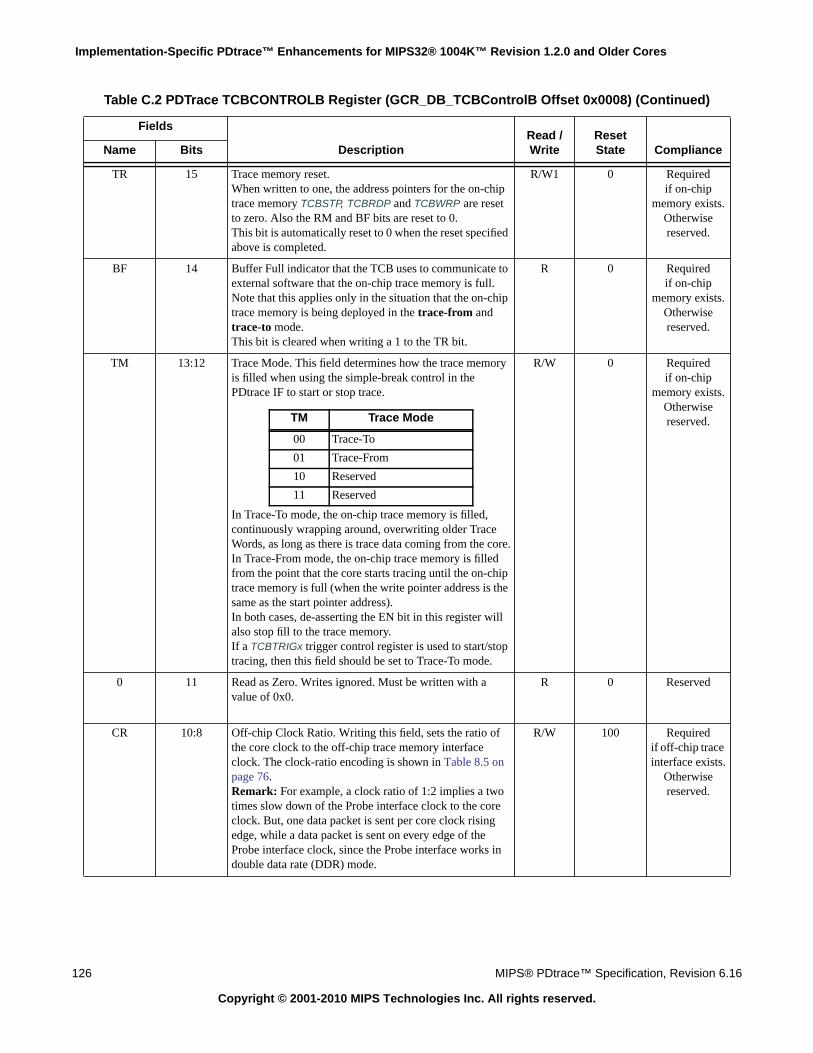
Implementation-Specific PDtrace™ Enhancements for MIPS32® 1004K™ Revision 1.2.0 and Older Cores
TR 15 Trace memory reset.When written to one, the address pointers for the on-chiptrace memory TCBSTP, TCBRDP and TCBWRP are resetto zero. Also the RM and BF bits are reset to 0.This bit is automatically reset to 0 when the reset specifiedabove is completed.
R/W1 0 Requiredif on-chip
memory exists.Otherwisereserved.
BF 14 Buffer Full indicator that the TCB uses to communicate toexternal software that the on-chip trace memory is full.Note that this applies only in the situation that the on-chiptrace memory is being deployed in the trace-from andtrace-to mode.This bit is cleared when writing a 1 to the TR bit.
R 0 Requiredif on-chip
memory exists.Otherwisereserved.
TM 13:12 Trace Mode. This field determines how the trace memoryis filled when using the simple-break control in thePDtrace IF to start or stop trace.
In Trace-To mode, the on-chip trace memory is filled,continuously wrapping around, overwriting older TraceWords, as long as there is trace data coming from the core.In Trace-From mode, the on-chip trace memory is filledfrom the point that the core starts tracing until the on-chiptrace memory is full (when the write pointer address is thesame as the start pointer address).In both cases, de-asserting the EN bit in this register willalso stop fill to the trace memory.If a TCBTRIGx trigger control register is used to start/stoptracing, then this field should be set to Trace-To mode.
R/W 0 Requiredif on-chip
memory exists.Otherwisereserved.
0 11 Read as Zero. Writes ignored. Must be written with avalue of 0x0.
R 0 Reserved
CR 10:8 Off-chip Clock Ratio. Writing this field, sets the ratio ofthe core clock to the off-chip trace memory interfaceclock. The clock-ratio encoding is shown in Table 8.5 onpage 76.Remark: For example, a clock ratio of 1:2 implies a twotimes slow down of the Probe interface clock to the coreclock. But, one data packet is sent per core clock risingedge, while a data packet is sent on every edge of theProbe interface clock, since the Probe interface works indouble data rate (DDR) mode.
R/W 100 Requiredif off-chip traceinterface exists.
Otherwisereserved.
Table C.2 PDTrace TCBCONTROLB Register (GCR_DB_TCBControlB Offset 0x0008) (Continued)
Fields
DescriptionRead /Write
ResetState ComplianceName Bits
TM Trace Mode
00 Trace-To
01 Trace-From
10 Reserved
11 Reserved
126 MIPS® PDtrace™ Specification, Revision 6.16
Copyright © 2001-2010 MIPS Technologies Inc. All rights reserved.

C.1 On-Chip Trace Memory
Cal 7 Calibrate off-chip trace interface.If set, the off-chip trace pins will produce the followingpattern in consecutive trace clock cycles. If more than 4data pins exist, the pattern is replicated for each set of 4pins. The pattern repeats from top to bottom until the Calbit is de-asserted.
Note: The clock source of the TCB and PIB must be run-ning.
R/W 0 Requiredif off-chip traceinterface exists.
Otherwisereserved.
0 6:2 Read as Zero. Writes ignored. Must be written with avalue of 0x0.
R 0 Reserved
OfC 1 If set to 1, trace is sent to off-chip memory using TR_DATApins.If not set, trace info is sent to on-chip memory.This bit is read only if either off-chip or on-chip optionexists.
R/W Preset Required
0 0 Read as Zero. Writes ignored. Must be written with avalue of 0x0.
R 0 Reserved
Table C.2 PDTrace TCBCONTROLB Register (GCR_DB_TCBControlB Offset 0x0008) (Continued)
Fields
DescriptionRead /Write
ResetState ComplianceName Bits
Calibrations pattern
3 2 1 0
Thi
s pa
ttern
is r
eplic
ated
for
eve
ry 4
bits
ofT
R_D
ATA
pin
s.
0 0 0 0
1 1 1 1
0 0 0 0
0 1 0 1
1 0 1 0
1 0 0 0
0 1 0 0
0 0 1 0
0 0 0 1
1 1 1 0
1 1 0 1
1 0 1 1
0 1 1 1
MIPS® PDtrace™ Specification, Revision 6.16 127
Copyright © 2001-2010 MIPS Technologies Inc. All rights reserved.

Implementation-Specific PDtrace™ Enhancements for MIPS32® 1004K™ Revision 1.2.0 and Older Cores
C.1.2 CM PDTrace TCB ControlE Register
NOTE: This section only applies to 1004K Releases 1.2.0 (PRID Revision Field = 0x28) and older. For 1004KRelease 1.3.0 (PRID Revision Field = 0x2c) and newer, please refer to Appendix B, “PDtrace™ Enhancementsfor Chip-Multiprocessing Systems” on page 112.
Similarly, TCBControlE is also modified from the single-core version to only have the status bits related to the on-chip trace buffer.
C.2 Software Control of Coherence Manager Trace
NOTE: This section only applies to 1004K Releases 1.2.0 (PRID Revision Field = 0x28) and older. For 1004KRelease 1.3.0 (PRID Revision Field = 0x2c) and newer, please refer to Appendix B, “PDtrace™ Enhancementsfor Chip-Multiprocessing Systems” on page 112.
As previously mentioned, the Coherence Manager itself can generate trace information. Software control of this traceinformation is enabled through the CMTraceControl register in the GCR register space (Debug Control Block, offset0x0010). This register is very similar to the TCBControlD register and is described below. A coherent core that imple-ments revision 6.00 and above of the PDtrace architecture also provides software access to the TCBControlD registervia drseg.
Figure C-1 CMTraceControl Register Format
Table C.3 TCBCONTROLE Register (GCR_DB_PD_TCBCONTROLE Offset 0x0020)
Fields
DescriptionRead /Write
ResetState ComplianceName Bits
0 31:9 Reserved for future use. Must be written as zero; returnszero on read.
0 0 Reserved
TrIDLE 8 Trace Unit Idle. This bit indicates if the trace hardware iscurrently idle (not processing any data). This can be usefulwhen switching control of trace from hardware to softwareand vice versa. The bit is read-only and updated by thetrace hardware.
R 1 Required afterrevision 06.00
and higher
0 7:0 Reserved for future use; Must be written as zero; returnszero on read. (Hint to architect: Reserved for future expan-sion of performance counter trace events).
0 0 Reserved
31 26 25 24 23 22 21 20 19 18 17 16 15 12 11 8 7 6 5 4 3 2 1 0
Impl ReservedTW
SrcValWB 0 IO TLev AE
SW_Trace_ON
CM_En
Table C.4 CMTraceControl Register Field Descriptions
Fields
DescriptionRead /Write
ResetState ComplianceName Bits
Impl 31:16 Reserved for implementations. Check core documentation Undefined Optional
128 MIPS® PDtrace™ Specification, Revision 6.16
Copyright © 2001-2010 MIPS Technologies Inc. All rights reserved.

C.2 Software Control of Coherence Manager Trace
Reserved 15:13 Reserved for future use. Must be written as 0, and read as 0 0 0 Required
TWSrcVal 11:8 The source ID of the CM. 0 0 Required
WB 7 When this bit is set, Coherent Writeback requests are traced.If this bit is not set, all Coherent Writeback requests are sup-pressed from the CM trace stream
R/W 0 Required
Reserved 6 Reserved for future use. Must be written as 0, and read as 0 0 0 Required
IO 5 Inhibit Overflow on CM FIFO full condition. Will stall theCM until forward progress can be made
R/W Undefined Required
TLev 4:3 This defines the current trace level being used by CM trac-ing.
R/W Undefined Required
AE 2 When set to 1, address tracing is always enabled for the CM.This affects trace output from the serialization unit of theCM.
R/W 0 Required
SW_Trace_ON
1 Setting this bit to 1 enables tracing from the CM as long asthe CM_EN bit is also enabled.
R/W 0 Required
CM_EN 0 This is the master trace enable switch to the CM. Whenzero, tracing from the CM is always disabled. When set toone, tracing is enabled whenever the other enabling func-tions are also true.
R/W 0 Required
Table C.4 CMTraceControl Register Field Descriptions (Continued)
Fields
DescriptionRead /Write
ResetState ComplianceName Bits
Encoding Meaning
00 No Timing Information
01 Include Stall Times, Causes
10 Reserved
11 Reserved
MIPS® PDtrace™ Specification, Revision 6.16 129
Copyright © 2001-2010 MIPS Technologies Inc. All rights reserved.

Appendix D
Implementation-Specific PDtrace™ Enhancements for theMIPS32® 1074K™ Cores
The Content of this Appendix has been moved to Appendix B, “PDtrace™ Enhancements for Chip-MultiprocessingSystems” on page 112. The reason for this is that both the 1004K and 1074K products lines now share the sameaccess method (the Trace-Master JTAG TAP controller) for the PDtrace control registers.
MIPS® PDtrace™ Specification, Revision 6.16 130
Copyright © 2001-2010 MIPS Technologies Inc. All rights reserved.

MIPS® PDtrace™ Specification, Revision 6.16 131
Copyright © 2001-2010 MIPS Technologies Inc. All rights reserved.

Appendix E
Tracing Multi-Issue and High Performance Processors
This section of the PDtrace specification is now designated as an Appendix, because it is no longer clear if thismethod for tracing multi-issue pipelines is useful and will ever be implemented. This method may be deprecated fromthe specification in a future release.
E.1 Background on High Performance Processors
This section addresses the tracing needs of multi-issue pipeline processors and describes a mechanism that allows aworkable and efficient tracing of program execution on such processors. The features of high performance processorsare not, in general, very suitable for effectively tracing the sequential execution of a program. Such processor featuresinclude, but are not limited to:
• Superscalar or multi-issue
• Aggressive, out-of-order dynamic scheduling with large fetch and issue windows
• Deep pipelines
• Multi-latency pipelines
• Multiple outstanding load misses
A processor that is designed to issue multiple instructions, and, moreover, out of order from the original programsequence, will also implement what is typically known as the re-order buffer. This re-order buffer and its control logicis responsible for putting the issued instructions back in-order (of the original program sequence). There is a stage inthe pipeline when instructions are graduated from the re-order buffer, i.e., the point where it is certain that the instruc-tion will not stop due to an exception (or any other reason), and can proceed to completion. This graduation ofinstructions from the re-order buffer is done in program sequence.
There are several things to note here. First, the graduated instructions have not completed their execution and willproceed to do so further in the pipeline; for example, the register write-back of the computed result of an arithmeticinstruction will happen later in the pipeline. The second thing to note is that, typically, the number of graduatinginstructions will not exceed the number of issue slots of the processor. But the number can vary from a minimum ofzero up to the number of issue slots at the front of the pipe, plus the number of load miss completions from the busand cache units, etc.
E.2 Basic Tracing Methodology
The trace methodology described in this document proposes that instructions be traced at the point of graduation. It isrecommended that a number of instructions be simultaneously traced, and that the recommended number is the num-ber of issue slots of the processor—let us call this the “number of instruction trace slots”. It is possible that in somecycles the number of graduating instructions is greater than the number of instruction trace slots. In these cases, theprocessor’s trace control logic must buffer the instruction(s) that could not be traced earlier, and trace them at the
MIPS® PDtrace™ Specification, Revision 6.16 132
Copyright © 2001-2010 MIPS Technologies Inc. All rights reserved.

E.2 Basic Tracing Methodology
beginning of the next cycle, still maintaining the program sequence order. Note that the size of such a buffer need notbe very large, because over time the number of issued instructions will equal the number of graduated instructions.The size of this buffer can be calculated based on the maximum number of instructions that can graduate from the re-order buffer on any given cycle, and this number is based on the processor’s pipeline depth and other pipeline-relatedfactors.
All the signals marked “Out” are signals output from the processor core and represent the activity of a single instruc-tion within the core. Most of these signals need to be duplicated as many times as the number of instruction trace slotswithin the core. Signals that must be duplicated are shown in Table F.1 also with signal names appended with a “_n”,where n is used to designate the instruction trace slot number. For example, a two-issue core can trace two instruc-tions and use InsComp_0 and InsComp_1 to represent the completion status values of two simultaneously graduatinginstructions. If only one instruction graduates on any given cycle, then InsComp_1 has a value of 000. When noinstruction graduates on a given cycle, then both InsComp_0 and InsComp_1 have 000 values.
The same example code fragment from before is shown in Table E.1 and this table shows the graduation cycle of eachinstruction and the number of the instruction trace slot that actually traces that instruction. This example assumes asimple two-issue processor that allows up to one load/store instruction per issue and one branch instruction per cycle.
Table E.1 Example Code Fragment Showing the Graduation Cycle and Trace Bus Number
InstrNo. PC Instruction
GraduationCycle Slot Number
1 0x00400188 SW $6, 0xe170($1) n+0 0
2 0x0040018c SW $4, 0xb134($28) n+1 0
3 0x00400190 SW $5, 0xb130($28) n+2 0
4 0x00400194 SW $0, 0x1c($29) n+3 0
5 0x00400198 JAL 0x418d9c n+4 0
6 0x0040019c OR $30, $0, $0 n+4 1
7 0x00418d9c NOP n+5 0
8 0x00418da0 JR $31 n+5 1
9 0x00418da4 NOP n+6 0
10 0x004001a0 JAL 0x411c40 n+7 0
11 0x004001a4 NOP n+7 1
12 0x00411c40 JR $31 n+8 0
13 0x00411c44 NOP n+8 1
14 0x00414adc LW $4, 0xb134($28) n+9 0
15 0x00414ae0 BEQ $14, $0, 0x414af8 n+9 1
16 0x00414ae4 ADDIU $29, $29, 0xffe0 n+10 0
17 0x00414af8 OR $7, $0, $0 n+10 1
18 0x00414afc NOP n+11 0
19 0x00414b00 ADDU $6, $6, $2 n+11 1
20 0x00414b04 OR $7, $2, $0 n+12 0
21 0x00414b08 SLTU $1, $2, $1 n+12 1
MIPS® PDtrace™ Specification, Revision 6.16 133
Copyright © 2001-2010 MIPS Technologies Inc. All rights reserved.

Tracing Multi-Issue and High Performance Processors
E.3 Coordinating Instruction Completion Trace with Address/Data Trace
When an instruction is traced on a particular instruction trace slot, say using InsComp_k, then all other information
for that instruction is sent on the signals of the “k”th instruction trace slot. For example, the address and data, if any,associated with that instruction is sent on the same slot. Thus, once an instruction begins its trace life on a particularinstruction trace slot, it must complete its life on the same slot. The exception to this occurs when the data is notimmediately available. In this situation, the data can be sent on any of the slots that is temporarily free and hence cho-sen by the processor to send that data. See E.4 “Out-of-Order Loads and Stores in the Multi-Pipe Core”.
The process of identifying the data associated with particular instructions has been simplified by making it a require-ment that all the data associated with instructions traced on the same cycle be in lock-step. Specifically, all the dataassociated with instructions that are traced together on the different InsComp_n are such that their end points (i.e., thelast data cycle) are synchronized to be traced together. This requirement makes it easier for an external block tosequence all the data operations into the program sequence. An example that illustrates this behavior is shown inFigure E.1.
Figure E.1 An Example Showing the Coordination of Instructions and Their Data
(1) (2)
Program Sequence InsComp_0 InsComp_1 cycle
ILBa ILBa ILb n
ILb ISc ILd n+1
ISc
ILd
(3)
Cycle TType_0 TType_1 TEnd_0 TEnd_1 Comments
m+0 TPCa1 NT 0 x
m+1 TPCa2 NT 1 x
m+2 TLAa1 NT 0 x
m+3 TLAa2 TLAb1 1 1
m+4 TDa1 TDb1 0 0
m+5 TDa2 TDb2 1 1completion of all TTypetransfers for instructions
traced in cycle n
m+6 TSAc1 NT 0 x
m+7 TSAc2 TLAd1 1 1
m+8 TDc1 TDd1 0 0
m+9 TDc2 TDd2 1 1completion of all TTypetransfers for instructions
traced in cycle n+1
(4)
Data in Program Sequence
134 MIPS® PDtrace™ Specification, Revision 6.16
Copyright © 2001-2010 MIPS Technologies Inc. All rights reserved.

E.4 Out-of-Order Loads and Stores in the Multi-Pipe Core
Figure E.1 shows four blocks of information. The first one (1) shows the instruction complete (InsComp) values inthe program sequence. The second block (2) shows these values as they would be transmitted on the two instructiontrace slots, i.e., InsComp_0 and InsComp_1. The third block (3) shows the TType and TEnd values for the two traceslots. Note that the data trace information for the instructions that were simultaneously traced on InsComp_0 andInsComp_1 are traced such that their TEnd is coordinated. For the InsComp values traced in cycle n (in block (2)), thedata transmission ends in cycle m+5 (in block (3)). And for the InsComp values traced in cycle n+1 (in block (2)), thedata transmission ends in cycle m+9 (in block (3)).
The external block reading the signals on the interface can then take the data values, and knowing the programsequence order (in block (1)), can put the data trace in order, as shown in block (4).
E.4 Out-of-Order Loads and Stores in the Multi-Pipe Core
When a multi-pipe core needs to send out-of-order data, it uses the DataOrder signal just like the single-pipe core.When an out-of-order data is returned, it can be traced on any free slot, not necessarily the one that traced the corre-sponding instruction. This is because instruction tracing is sequentialized by the InsComp_n order, and therefore thedata can be associated with the correct instruction once the DataOrder value is known. Note that since the slots areimplicitly ordered, for data transmissions that end on the same cycle, the data on TType_k is before the data onTType_k+1.
E.5 Tagging Instructions that Issue Together
With the method of tracing graduating instructions in sequence, it is not possible to know which instructions issuetogether without additional information. This information might be invaluable to tune a code optimizer for high per-formance processors. In order to trace this information, the processor tags all the instructions that issue together,using the signal IssueTag_n. This tag value is also traced out with each InsComp_n value. A tag value of 6 bits isbeing initially proposed, assuming an issue window of about 64 instructions. Note that this tag information can betraced out of the TCB only if the user requires it, hence it will not incur bandwidth on the external pins unless there isa real need for this information. Thus, it is recommended that the TCB allow the external tracing of this informationunder user discretion.
E.6 Miscellaneous
Tracing from each one of the multiple pipelines is controlled by the same set of bits, either in CP0 or in the TCB, aswell be described in other chapters.
TPCa1, TPCa2,
TLAa1, TLAa2,
TLAb1,
TDa1, TDa2
TDb1, TDb2
TSAc1, TSAc2
TLAd1
TDc1, TDc2
TDd1, TDd2
MIPS® PDtrace™ Specification, Revision 6.16 135
Copyright © 2001-2010 MIPS Technologies Inc. All rights reserved.

Tracing Multi-Issue and High Performance Processors
When tracing is first started (or re-started after a break), InsComp_0 is the first traced instruction in the static programimage and this will output the TMOAS record and the full PC.
When there is a need for synchronization, the core can choose any InsComp_n to send the TMOAS record and thefull PC value, as long as these two are both done on the same instruction in the trace slot. Note that if load/storeaddresses are also being traced, then a full load/store address value is part of the synchronization tracing. This maynot always be possible on the instruction chosen by the core. But these should be sent on the next sequential load/store instruction. This is a situation that the external software has to take into account when recognizing synchroniza-tion transmissions in the multi-pipeline core or processor.
136 MIPS® PDtrace™ Specification, Revision 6.16
Copyright © 2001-2010 MIPS Technologies Inc. All rights reserved.

Appendix F
PDtrace™ Interface Signals (The Interface is nowDeprecated as Architecture and this Chapter is here Solelyfor Historical Reasons)
All signals are assumed to be asserted high unless otherwise noted. The signal direction “Out” refers to a signal that isoutput from the processor core or coherence manager, and “In” signals are those that are input to the processor core orcoherence manager. The “PDO_” prefix to the signal names is used to uniquely identify the signals as belonging tothe PDtrace Output interface. And the “PDI_” prefix is used to identify the PDtrace Input signals. Signals that havebeen repeated in the “Signal Name” column with a “_n” prefix are PDO_ signals that are to be duplicated for multi-issue processors.
MIPS® PDtrace™ Specification, Revision 6.16 137
Copyright © 2001-2010 MIPS Technologies Inc. All rights reserved.
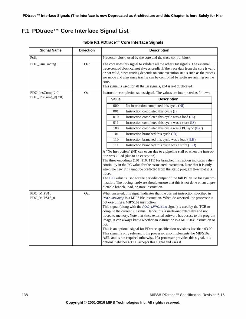
PDtrace™ Interface Signals (The Interface is now Deprecated as Architecture and this Chapter is here Solely for His-
F.1 PDtrace™ Core Interface Signal List
Table F.1 PDtrace™ Core Interface Signals
Signal Name Direction Description
Pclk Processor clock, used by the core and the trace control block.
PDO_IamTracing Out The core uses this signal to validate all the other Out signals. The externaltrace control block cannot always predict if the trace data from the core is validor not valid, since tracing depends on core execution status such as the proces-sor mode and also since tracing can be controlled by software running on thecore.This signal is used for all the _n signals, and is not duplicated.
PDO_InsComp[2:0]PDO_InsComp_n[2:0]
Out Instruction completion status signal. The values are interpreted as follows:
A "No Instruction" (NI) can occur due to a pipeline stall or when the instruc-tion was killed (due to an exception).The three encodings (101, 110, 111) for branched instruction indicates a dis-continuity in the PC value for the associated instruction. Note that it is onlywhen the new PC cannot be predicted from the static program flow that it istraced.The IPC value is used for the periodic output of the full PC value for synchro-nization. The tracing hardware should ensure that this is not done on an unpre-dictable branch, load, or store instruction.
PDO_MIPS16PDO_MIPS16_n
Out When asserted, this signal indicates that the current instruction specified inPDO_InsComp is a MIPS16e instruction. When de-asserted, the processor isnot executing a MIPS16e instruction.This signal (along with the PDO_MIPS16Ins signal) is used by the TCB tocompute the current PC value. Hence this is irrelevant externally and nottraced to memory. Note that since external software has access to the programimage, it can always know whether an instruction is a MIPS16e instruction ornot.This is an optional signal for PDtrace specification revisions less than 03.00.This signal is only relevant if the processor also implements the MIPS16eASE, and is not required otherwise. If a processor provides this signal, it isoptional whether a TCB accepts this signal and uses it.
Value Description
000 No instruction completed this cycle (NI)
001 Instruction completed this cycle (I)
010 Instruction completed this cycle was a load (IL)
011 Instruction completed this cycle was a store (IS)
100 Instruction completed this cycle was a PC sync (IPC)
101 Instruction branched this cycle (IB)
110 Instruction branched this cycle was a load (ILB)
111 Instruction branched this cycle was a store (ISB)
138 MIPS® PDtrace™ Specification, Revision 6.16
Copyright © 2001-2010 MIPS Technologies Inc. All rights reserved.

F.1 PDtrace™ Core Interface Signal List
PDO_MIPS16Ins[1:0]PDO_MIPS16Ins_n[1:0]
Out This signal accompanies the PDO_MIPS16 signal and is used to indicate thetype of MIPS16e instruction. Like PDO_MIPS16 this is optional, but must beimplemented if PDO_MIPS16 is implemented.
PDO_AD[15:0] orPDO_AD[31:0]PDO_AD_n[15:0] orPDO_AD_n[31:0]
Out The address or data value is transmitted on this bus. The actual values must becorrelated using the PDO_TType signal described below. It is recommendedthat a 64-bit processor core implement at least 32 bits for improved tracingcapability.A multi-cycle transaction sends the least-significant bits first, followed by themore-significant bits.When the transmitted data width is less than the width of the bus, the data istransmitted on the least-significant bits of the bus. There is no necessity toindicate the validity since the post-analyzing software knows the width of thedata. (For example, a LB implies one byte of data). The upper bits of the busmust be sign extended to allow the TCB to truncate the upper bits and henceavoid tracing unneeded bits to memory.
PDO_TType[2:0]PDO_TType_n[2:0]
Out Specifies the transmission type for the transaction on the PDO_AD lines. Thevalid types are:
Table F.1 PDtrace™ Core Interface Signals (Continued)
Signal Name Direction Description
Value Description
00 Is executing a MIPS16e instruction that is not a MACROinstruction and is not extended.
01 Is executing a MIPS16e instruction that is not a MACROinstruction and is extended.
10 Is executing a MIPS16e MACRO instruction.
11 Reserved
Value Description
000 No transmission this cycle (NT)
001 Transmitting the PC (TPC)
010 Transmitting the load address (TLA)
011 Transmitting the store address (TSA)
100 Transmitting the load/store data value (TD)
101 Transmitting the processor mode, the 8-bit ASID, and theSYNC bit. This is triggered by either a change in the proces-sor mode, by a software write to the EntryHi register, or atrace synchronization operation. (TMOAS). If the processordoes not implement the standard TLB-based MMU, it isUNPREDICTABLE whether a write to the EntryHi registertriggers a TMOAS operation. (See Figure 3.3).
110 Transmitting user-defined trace record - type 1 (TU1)
111 Transmitting user-defined trace record - type 2 (TU2)
MIPS® PDtrace™ Specification, Revision 6.16 139
Copyright © 2001-2010 MIPS Technologies Inc. All rights reserved.

PDtrace™ Interface Signals (The Interface is now Deprecated as Architecture and this Chapter is here Solely for His-
PDO_TEndPDO_TEnd_n
Out Indicates the last cycle of the current transaction on the PDO_AD bus. This sig-nal can be asserted in the same cycle that a transaction is started, implying thatthe particular transaction only took one cycle to complete.In a multi-issue core, the PDO_TEnd signals are synchronized for all thePDO_AD_n transmissions associated with instructions that graduate together.See Section E.3 “Coordinating Instruction Completion Trace with Address/Data Trace” on page 134 for details.In PDtrace revision 3.00 and higher, the processor is allowed to assert this sig-nal early if the tracing logic determines that the upper bits of the address ordata being sent on the PDO_AD bus are redundant. For example, redundantupper sign bits may be omitted and software could easily reconstruct thesebits. Note that the TCB must therefore be capable of accepting an earlyPDO_TEnd signal for any transmission type. This early assertion ofPDO_TEnd is allowed for all the values of PDO_TMode.
PDO_TModePDO_TMode_n
Out Indicates the transmission mode for the bits transmitted on PDO_AD. Themode depends on the transmission type.
Table F.1 PDtrace™ Core Interface Signals (Continued)
Signal Name Direction Description
PDO_TType PDO_TMode
000 (NT)101 (TMOAS)
Reserved
001 (TPC) 0 -> delta from last PC value1 -> compression algorithm A (full address)
010 (TLA)011 (TSA)
0 -> delta from last data address of that type1 -> compression algorithm B (full address)
100 (TD)110 (TU1)111 (TU2)
0 -> Reserved1 -> compression algorithm C (full data)
140 MIPS® PDtrace™ Specification, Revision 6.16
Copyright © 2001-2010 MIPS Technologies Inc. All rights reserved.

F.1 PDtrace™ Core Interface Signal List
PDO_DataOrder[3:0]PDO_DataOrder_n[3:0]
Out This signal is used to indicate the degree of out-of-order-ness of load and storedata. Using this order value allows load and store data to be traced out as itbecomes available, thus avoiding the need to internally buffer data. Note thatonly sixteen outstanding data values are allowed because of the limitationimposed by the signal width of 4 bits. This signal takes on the following val-ues:
PDO_TrigI[N:0] Out This vector indicates which of the N+1 implemented EJTAG hardware instruc-tion breakpoints caused a trigger. The instruction causing the trigger is indi-cated on the corresponding PDO_InsComp bus, if tracing has been turned on.Note that EJTAG restricts the maximum number of implementable hardwareinstruction breakpoints to 15.
PDO_TrigD[N:0] Out This vector indicates which of the N+1 implemented EJTAG hardware databreakpoints caused a trigger. The instruction causing the trigger is not neces-sarily the one on the PDO_InsComp bus since data triggers may be imprecise.Note that EJTAG restricts the maximum number of implementable hardwaredata breakpoints to 15.
PDO_TrigOn Out This bit is asserted if at least one trigger in PDO_TrigI[N:0] or PDO_TrigD[N:0]turns trace on. (See 3.16 “Trace Trigger from EJTAG Hardware Instruction/Data Breakpoints” on page 35).
PDO_TrigOff Out This is asserted if no trigger turns trace on (i.e., PDO_TrigOn is not asserted),and at least one of the indicated triggers in PDO_TrigI[N:0] or PDO_TrigD[N:0]turns trace off. (See 3.16 “Trace Trigger from EJTAG Hardware Instruction/Data Breakpoints” on page 35).
Table F.1 PDtrace™ Core Interface Signals (Continued)
Signal Name Direction Description
Value Description
0000 data from oldest load/store instruction (is in-order)
0001 data from second-oldest load/store instruction
0010 data from third-oldest load/store instruction
0011 data from fourth-oldest load/store instruction
0100 data from fifth-oldest load/store instruction
0101 data from sixth-oldest load/store instruction
0110 data from seventh-oldest load/store instruction
0111 data from eighth-oldest load/store instruction
1000 data from ninth-oldest load/store instruction
1001 data from tenth-oldest load/store instruction
1010 data from eleventh-oldest load/store instruction
1011 data from twelfth-oldest load/store instruction
1100 data from thirteenth-oldest load/store instruction
1101 data from fourteenth-oldest load/store instruction
1110 data from fifteenth-oldest load/store instruction
1111 data from sixteenth-oldest load/store instruction
MIPS® PDtrace™ Specification, Revision 6.16 141
Copyright © 2001-2010 MIPS Technologies Inc. All rights reserved.

PDtrace™ Interface Signals (The Interface is now Deprecated as Architecture and this Chapter is here Solely for His-
PDO_Overflow Out This signals an internal FIFO overflow error in the core and implies the fol-lowing:• the current transmission is to be abandoned in the current cycle• the FIFO is emptied so that previously collected trace information in the
FIFO is lost• a new transmission begins in the next cycle with a TMOAS and a full PC
address
PDO_ValidModes[1:0] Out This signal specifies the subset of tracing that is supported by the processor(see 2.3 “Subsetting” on page 17).
PDO_IssueTag_n[5:0] Out This signal is used in multi-issue processors and it is signaled withPDO_InsComp_n. In multi-issue processors, instructions that issue togetherare assigned a matching tag value, specified by this signal value.A six bit internal counter increments each cycle, and the instructions that issuein that cycle are assigned the counter value. When the maximum counter valueis reached, it simply restarts at zero.This feature facilitates the performance debugging of code schedulers forhigh-end processors. These tag values are available every cycle, but it is antici-pated that the TCB will trace this to memory only when specially requested bythe user.
PDO_IMissPDO_IMiss_n
Out When asserted, this signals whether the load or store instruction specified byPDO_InsComp in this cycle missed in the instruction cache during the fetchoperation. This signal is ignored if PDO_InsComp indicated that no instructioncompletes this cycle (i.e., when it is 000).
PDO_LSMissPDO_LSMiss_n
Out When asserted, this signals whether the load or store data specified byPDO_TType of TD in this cycle missed in the data cache during the data loador store operation. The data cache miss is indicated with the transmitted datarather than the instruction that caused the miss because in the pipeline a datacache miss cannot often be detected at the time that the instruction is transmit-ted with the appropriate PDO_InsComp value. It is the reconstruction softwarewhich needs to associate the data with the corresponding PC and data address.
PDO_FuncCRPDO_FuncCR_n
Out When asserted, this signal indicates that this instruction can potentially beeither a function call instruction or a function return instruction. See ChapterF, “PDtrace™ Interface Signals (The Interface is now Deprecated asArchitecture and this Chapter is here Solely for Historical Reasons)” onpage 137 for details.Note that it is possible for a single instruction to assert both PDO_IMiss as wellas this signal.
PDO_TC[7:0]PDO_TC_n[7:0]
Out For a processor that implements multithreading (MIPS MT ASE), and for avalid PDO_InsComp value (when not NI), this signal indicates the thread con-text number of the traced instruction. A given implementation only needs touse as many encoded bits for this signal as the total TCs implemented. Forexample, the 34Kc core with maximum 9 possible TCs will only require 4 bits.The PC delta value that is transmitted by the core is now maintained on a per-TC basis.
Table F.1 PDtrace™ Core Interface Signals (Continued)
Signal Name Direction Description
Encoding Meaning
00 PC tracing only
01 PC and load and store address tracing only
10 PC, load and store address, and load and store data
11 Reserved
142 MIPS® PDtrace™ Specification, Revision 6.16
Copyright © 2001-2010 MIPS Technologies Inc. All rights reserved.

F.1 PDtrace™ Core Interface Signal List
PDO_CPUid[7:0]PDO_CPUid_n[7:0]
Out Optional output for a processor indicating the processor number(Ebase.CPUNum) of the traced instruction. It would be used in a multi-coredesign, where the Ebase.CPUNum field for the core is used to tag the tracefrom different cores in the multi-core environment. If the core were not imple-mented in a multi-core design, then the TCB would simply ignore the value onthis signal.
PDO_COSId[1:0] Out Coherent Synchronization ID. This is a 2-bit value used to synchronize coretrace messages with trace messages received from the coherent interconnect.Required for all processors using PDtrace specification 5.00 and higher.
PDI_TCBPresent In When asserted this indicates that the TCB hardware is present and connectedto the core’s tracing logic. Hence the core can consider the other PDI_ signalsto be valid.
PDI_TraceOn In This is the signal asserted by the external trace block into the core that stateswhether tracing is globally turned on or off. It is expected that this signal becontinuously asserted to turn on tracing.0 : Tracing off1 : Tracing is turned on
PDI_TraceMode[4:0] In When tracing is turned on, this signal specifies what information is to be tracedby the core. It uses 5 bits, where each bit turns on tracing for a specific tracingmode. The table shows what trace value is turned on when that bit value is a 1.
If the corresponding bit is 0, then the Trace Value shown in column two is nottraced by the processor. This implementation is required for all processorsusing PDtrace specification 4.00 and higher.Obviously, the processor has to support the tracing mode that is beingrequested for this input signal to have any effect. For example, if the processoronly supports PC tracing, then only bit 0 is read by the processor, and otherother bits are ignored, and so on. Which bits are ignored and which are readcan be obtained by reading the PDO_ValidModes output signal.It is optional for an implementation to allow PC tracing to be turned off. Thismust be clearly documented by the core implementation-specific document.When it is optional, bit 0 is tied to a value of 1 and setting bit 0 to 0 is simplyignored by the processor.
PDI_G In The global bit, which if asserted to 1, implies that all processes are to betraced. If 0, then trace data is sent only for a process that matchesPDI_ASID[7:0]. If the processor does not implement the standard TLB-basedMMU, this signal is ignored by the processor and is treated as if it wereasserted.
PDI_ASID[7:0] In When the global bit is 0, only the process whose ASID matches this ASIDvalue will be traced. If the processor does not implement the standard TLB-based MMU, this signal is ignored by the processor.
Table F.1 PDtrace™ Core Interface Signals (Continued)
Signal Name Direction Description
Bit # Set Trace The Following
0 PC
1 Load address
2 Store address
3 Load data
4 Store data
MIPS® PDtrace™ Specification, Revision 6.16 143
Copyright © 2001-2010 MIPS Technologies Inc. All rights reserved.

PDtrace™ Interface Signals (The Interface is now Deprecated as Architecture and this Chapter is here Solely for His-
PDI_U In Enables tracing in User Mode (see 2.2 “Processor Modes” on page 16). Thisenables tracing only if the PDI_TraceOn is also asserted or the hardware break-point trace triggers on, and either the PDI_G bit is set or the PDI_ASID matchesthe current process ASID.
PDI_S In Enables tracing in Supervisor Mode (for those processors that implementSupervisor Mode), otherwise, this signal is not required (see 2.2 “ProcessorModes” on page 16). This enables tracing only if the PDI_TraceOn is alsoasserted or the hardware breakpoint trace triggers on, and either the PDI_G bitis set or the PDI_ASID matches the current process ASID.
PDI_K In Enables tracing in Kernel Mode (see 2.2 “Processor Modes” on page 16).This enables tracing only if the PDI_TraceOn is also asserted or the hardwarebreakpoint trace triggers on, and either the PDI_G bit is set or the PDI_ASIDmatches the current process ASID.
PDI_E In Enables tracing when in Exception Mode (see 2.2 “Processor Modes” onpage 16). This enables tracing only if the PDI_TraceOn is also asserted or thehardware breakpoint trace triggers on, and either the PDI_G bit is set or thePDI_ASID matches the current process ASID.
PDI_DM In Enables tracing in Debug Mode (see 2.2 “Processor Modes” on page 16). Thisfeature is useful to debug the debug handler code via the EJTAG and TAP con-troller port.
PDI_InhibitOverflow In This signal is used by the external trace block to indicate to the core that thecore pipeline should be back-pressured (and stalled) instead of allowing thetrace FIFO to overflow and hence lose trace information.
PDI_StallSending In When asserted, this signal is used by the external trace block to indicate to thecore that it must stop transmitting trace information in the next cycle. Thisrequest may be essential when the trace control block is in imminent danger ofover-running its internal trace buffer.In the cycle when the signal is asserted, the value on all the PDO_ signals arevalid and must be captured by the TCB.In the cycle after the one where the core sees an assertion of this signal thecore must not transmit any valid trace information on any of the PDO_ outputsignal bits (including PDO_InsComp).In the cycle after the TCB de-asserts this signal again, PDtrace PDO_ signalsare valid and must be captured by the TCB. (Note that some processors cannotarbitrarily stall their pipeline on any given cycle. In this situation, the imple-mentation on the processor side must provide sufficient buffering to hold traceinformation until the pipeline can be stalled).
PDI_SyncOffEn In This signal is an enable signal for the PDI_SyncPeriod, PDI_TBImpl, andPDI_OffChipTB signals. When asserted, the core latches these values. This sig-nal, and the signals which it controls must be asserted before tracing can begin.
Table F.1 PDtrace™ Core Interface Signals (Continued)
Signal Name Direction Description
144 MIPS® PDtrace™ Specification, Revision 6.16
Copyright © 2001-2010 MIPS Technologies Inc. All rights reserved.

F.1 PDtrace™ Core Interface Signal List
PDI_SyncPeriod[2:0] In This signal is used to set the synchronization period bits in the TraceControl2register. The value specifies the period (in cycles) for sending synchronizationinformation.
PDI_TBImpl In When this signal is a 1, the TCB has implemented both an on-chip and an off-chip trace buffer, and the PDI_OffChipTB signal indicates to which the trace iscurrently being written. When this signal is a 0, the PDI_OffChipTB signal indi-cates which buffer is implemented. This value is written into the TraceControl2CP0 register (as the TBI bit). It is optional for the TCB to provide this signal tothe core logic for all TCB implementations compatible to PDtrace specifica-tions less than 03.00.
PDI_OffChipTB In When one, this signal indicates that the trace data is being sent off-chip to anexternal trace memory. When zero, this indicates an on-chip trace buffer. Thevalue of this signal to the core changes how the core interprets the trace syn-chronization period bits. This signal value is written into the TraceControl2CP0 register (as the TBU bit).
PDI_TraceAllBranch In When asserted, the core’s tracing logic will emit PC values for all takenbranches encountered in the execution stream, including all conditional andunconditional, predictable and unpredictable branches. When de-asserted, thecore reverts to normal tracing mode.
PDI_TraceIMiss In When asserted, PDO_IMiss is set when the processor detects an instructioncache miss for the current instruction being traced. Like all other trace signals,this input signal causes active tracing only when tracing is currently turned on.If PDI_TraceMode[0], i.e., bit 0 is turned off, that is, no PC tracing has beenrequested, then a PDO_IMiss assertion is accompanied by a full PC value. Oth-erwise there is no special action taken for this instruction other than assertingthe PDO_IMiss bit.
PDI_TraceLSMiss In When asserted, when PDO_LSMiss is set when the processor detects a datacache miss on a load or a store. Like all other trace signals, this input signalcauses active tracing only when tracing is currently turned on.If PDI_TraceMode[0] is turned off, that is PC tracing is disabled, then the PC ofthe missed instruction will not be available to the reconstruction software. IfPDI_TraceMode[1] or PDI_TraceMode[2] is turned off, that is no data addresstracing is enabled, then no data address is traced for the address that missed inthe cache. Even if PDI_TraceMode[3] or PDI_TraceMode[4] is turned off, thefull data value for the missed instruction is traced out.
Table F.1 PDtrace™ Core Interface Signals (Continued)
Signal Name Direction Description
SyncPeriodPeriod (in cycles) for sending
sync records
000 25
001 26
010 27
011 28
100 29
101 210
110 211
111 212
MIPS® PDtrace™ Specification, Revision 6.16 145
Copyright © 2001-2010 MIPS Technologies Inc. All rights reserved.

PDtrace™ Interface Signals (The Interface is now Deprecated as Architecture and this Chapter is here Solely for His-
PDI_TraceFuncCR In When asserted, PDO_FuncCR is set when the current instruction could be afunction call or return instruction. Like all other trace signals, this input signalcauses active output tracing only when tracing is turned on.If PDI_TraceMode[0], i.e., bit 0 is turned off, that is, no PC tracing has beenrequested, then a PDO_IMiss assertion is accompanied by a full PC value. Oth-erwise there is no special action taken for this instruction other than assertingthe PDO_IMiss bit.
PDI_TCNum[7:0] In Only implemented in a processor with MT. When PDI_TCNumValid isasserted, this signal gives the number of the Thread Context that is to betraced. Only the number of bits required to encode the total TC number isimplemented. As long as PDI_TraceTCValid is asserted, no instruction fromany other thread is traced. If the required TC does not execute any instructions,then no instructions are traced, the PDO_InsComp value will remain NI. Wheninstructions from other TCs are executed, these are marked as NI on thePDtrace interface.
PDI_TCNumValid In Only implemented in a processor with MT. When asserted, the PDI_TCNumsignal is taken by the processor and used as the number of the TC whoseinstructions are to be traced. This signal must remain asserted as long as trac-ing is required from a specific TC. If not asserted, then tracing reverts to otherconditions being fulfilled.
PDI_CPUId[7:0] In Implemented in a processor with MT, where this signal gives the number ofthe VPE that is to be traced, if PDI_CPUIdValid is asserted. As long asPDI_VPENumValid is asserted, no instruction from any other VPE is traced. Ifthe required VPE does not execute any instructions, then no instructions aretraced, the PDO_InsComp value will remain NI. When instructions from otherVPEs are executed, these are marked as NI on the PDtrace interface. This bit isignored if TCNumValid is asserted.In a multi-core processor SOC environment, this specifies the id of the proces-sor that is to be traced if PDI_CPUIdValid is asserted.
PDI_CPUIdValid In Only implemented in a processor with MT or in a multi-core SOC implemen-tation. When asserted, the PDI_CPUId signal is taken by the processor andused as the number of the VPE (or core) whose instructions are to be traced.This bit is ignored if TCNumValid is asserted.
Table F.1 PDtrace™ Core Interface Signals (Continued)
Signal Name Direction Description
146 MIPS® PDtrace™ Specification, Revision 6.16
Copyright © 2001-2010 MIPS Technologies Inc. All rights reserved.

F.1 PDtrace™ Core Interface Signal List
F.1.0.1 PDtrace Coherence Manager Interface Signals
Table F.2 PDtrace Coherence Manager Interface Signals
Signal Name Direction Width Description
COSId_n Input 2 COSId input received from processor core. One copy of signal per core
SRH_SrcPort Output 3 Source of the request that was serialized
SRH_COSId Output 2 Coherent Sync ID of transaction. Used to correlate CPU and CM transactions
SRH_MCmd Output 5 Command in the request that was serialized (See Table F.3)
SRH_WaitTime Output 8 This is active only in timing mode. Tracks how many cycles the transaction spent stalledin the SRH. Saturates at 255 cycles.
SRH_Address Output 29 This is active when we are tracing addresses from the SRH - provides the address corre-sponding to the request being traced.
SRH_AddrTarg Output 3 Target of the current request (see Table F.4) (Indicates speculative reads as well)
IVU_COSId Output 2 Coherent Sync ID at the Intervention Unit
IVU_SrcPort Output 3 The core that made the original request that resulted in this intervention
IVU_RespBV Output 6 Bit vector of intervention port responses. Bit corresponding to a core is set to ‘1’ if theintervention hit, and set to ‘0’ if the intervention missed.
IVU_IntvResult Output 3 Global Intervention State for this cache line (see Table F.5)
IVU_SC_Cancel Output 1 This transaction was cancelled due to a previous SC Fail
IVU_SC_Failed Output 1 This intervention will cause a future SC to fail
IVU_PIQ_WaitTime Output 8 Cycle count that each transaction spends at the top of the PIQ. Saturates at 255
IVU_PIQ_StallCause Output 3 What was the last reason this transaction was stalled on top of the PIQ. (see Table F.6)
Table F.3 MCmd - OCP Commands
Value Command Description Value Command Description
0x00 IDLE 0x0C COH_UPGRADE Coherent Upgrade (SC bit == 0)
0x01 LEGACY_WR_UC Uncached legacy write, CCA=UC,UCA, WT
0x0D COH_WB Coherent Writeback
0x02 LEGACY_RD_UC Uncached legacy read, CCA = UC 0x10 COH_COPYBACK Coherent Copyback
0x03 LEGACY_WR_WB Cached legacy write, CCA = WB 0x11 COH_COPYBACKINV Coherent Copyback Invalidate
0x04 LEGACY_RD_WB Cached legacy read, CCA = WB, WT 0x12 COH_INV Coherent Invalidate
0x05 LEGACY_SYNC Uncached legacy read with MRe-qInfo[3] == 1
0x13 COH_WR_INV Coherent Write Invalidate
0x06 L2_L3_CACHEOP_WR
Uncached legacy write with MAd-drSpace != 0
0x14 COH_CMPL_SYNC Coherent Completion Sync withMReqInfo[3] == 0
0x07 L2_L3_CACHEOP_RD
Uncached legacy read with MAd-drSpace != 0
0x15 COH_CMPL_SYNC_MEM
Coherent Completion Sync withMReqInfo[3] == 1
0x08 COH_RD_OWN Coherent Read Own 0x17 COH_WR_INV_FULL Coherent Invalidate due to a full line
0x09 COH_RD_SHR Coherent Read Shared 0x18 COH_RD_OWN_SC Coherent Read own with SC bit == 1
0x0A COH_RD_DISCARD Coherent Read Discard 0x1C COH_UPGRADE_SC Coherent Upgrade with SC bit == 1
0x0B COH_RD_SHR_ALWAYS
Coherent Read Share Always
MIPS® PDtrace™ Specification, Revision 6.16 147
Copyright © 2001-2010 MIPS Technologies Inc. All rights reserved.
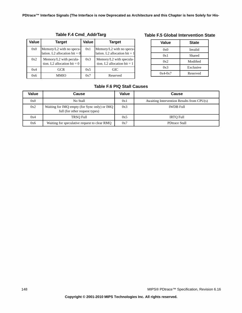
PDtrace™ Interface Signals (The Interface is now Deprecated as Architecture and this Chapter is here Solely for His-
Table F.4 Cmd_AddrTarg
Value Target Value Target
0x0 Memory/L2 with no specu-lation. L2 allocation bit = 0
0x1 Memory/L2 with no specu-lation. L2 allocation bit = 1
0x2 Memory/L2 with pecula-tion. L2 allocation bit = 0
0x3 Memory/L2 with specula-tion. L2 allocation bit = 1
0x4 GCR 0x5 GIC
0x6 MMIO 0x7 Reserved
Table F.5 Global Intervention State
Value State
0x0 Invalid
0x1 Shared
0x2 Modified
0x3 Exclusive
0x4-0x7 Reserved
Table F.6 PIQ Stall Causes
Value Cause Value Cause
0x0 No Stall 0x1 Awaiting Intervention Results from CPU(s)
0x2 Waiting for IMQ empty (for Sync only) or IMQfull (for other request types)
0x3 IWDB Full
0x4 TRSQ Full 0x5 IRTQ Full
0x6 Waiting for speculative request to clear RMQ 0x7 PDtrace Stall
148
Copyright © 2001-2010 MIPS Technologies
MIPS® PDtrace™ Specification, Revision 6.16
Inc. All rights reserved.

Appendix G
Revision History
Revision Date Description
1.6 August 29, 2000 Changes in this revision:Add the requirement that the data address be also periodically gathered forsynchronization purposes, per FS2.Modify Figure 3 to show that the load data is picked up after alignment,per lhh.typo fixes
1.7 September12, 2000 Changes in this revision:Add a separate input signal that says whether to trace in Debug mode ornot (i.e., DM = 1 in the Debug register), per Scott who wants to be able todebug the debug handler code.Put back Figure 3 to tap load/store data pre-alignment, per Franz.Add a section (3.17) to show when tracing is enabled.Allow the ASID to be masked under software control, per Scott.Amend Figure 1 to show the EJTAG/TAP controller and its connection tothe debugger.Add to Table 2, to show the use of the PDO_InsComp signal value IPC(100).Add a chapter (6) on the trace capture block and its interaction with theexternal debugger software.Add TOCFix typos, grammar, sentence construction.
1.8 October 27, 2000 Changes in this revision:Change the way loads are tracked and traced out.Add the tracing out of ASID and processor mode as part of the periodicsynchronization.Add details to the multi-issue tracing section.The above changes require a modification to the output format section.Add a chapter to discuss the trace capture block (TCB), that includes: adefinition of the control registers within the TCB, and the mechanism towrite these registers from the external probe (or debugger).Define tracing with an on-chip trace buffer versus off-chip trace buffer.Add another Out signal from the core, PDO_IamTracing, that the core usesto signal to the TCB that it is actually sending valid trace data.
1.9 November 20, 2000 Changes in this revision:Add tracing of processor ISA mode, and whether processor is in Debugmode or not.Get rid of the TCBTraceMask register, is not really needed.Allocate some bits in the TraceControl register as implementation depen-dent.Specify that full addresses are used for on-chip trace memory.Change the encoding of bits from the EJTAG logic to the tracing logic,send all 30 bits of breakpoint trigger.Fix the logical expression in 3.1.8.
MIPS® PDtrace™ Specification, Revision 6.16 149
Copyright © 2001-2010 MIPS Technologies Inc. All rights reserved.

Revision History
2.0 December 19, 2000 Changes in this revision:Add a signal from the TCB to the core tracing logic, PDI_StallSending,that inhibits the core from sending trace data. Note that the core does notstop tracing, only stops sending trace information to the TCB. Used by theTCB when its internal buffer is in imminent danger of overflowing. (Thecore will stall if its internal FIFO will overflow).Make the synchronization period programmable, by using some bits in aregister to hold this value. These bits can be updated by either software orby the TCB (based on the trace buffer size).Add a signal from the TCB to the core tracing logic that signals whetherthe TCB is using an on-chip or off-chip trace buffer. This changes the wayin which the core interprets the synchronization period bits in the register.The chapter on trace control block (TCB) has been cut off into anotherdocument, since it is not directly relevant to the PDtrace architecture.
2.01 January 25, 2001 Changes in this revision:Add a signal PDI_TCBPresent to indicate that the TCB hardware ispresent.Clearer explanation of how the PDI_StallSending signal works.Change in how the PDI_EXL and the corresponding X bit in the Trace-Control register works.Coding change in the PDI_TraceMode[2:0] signal.
2.02 February 12, 2001 Changes in this revision:Change in how the PDI_EXL and the corresponding X bit in the Trace-Control register works. Tracing triggers on when either EXL or the ERLbit is a 1, this enables tracing after a cold reset.
2.03 March 22, 2001 Changes in this revision:• Add a register description table for UserTraceData.• Add a PDI_TraceAllBranch signal to indicate that all branches (condi-
tional, unconditional, predictable, and unpredictable) are to be traced.• Change the PDO_InsComp definition for unconditional predictable
branches (jumps), so that these trace out as IB, ILB, and ISB (rather thanI, IL, and IS).
• Document how tracing is handled within MACRO instructions and theSAVE/RESTORE instruction.
• Document what happens when a mode change happens within the pro-cessor and this changes the tracing mode, i.e., either turns it off or on.
• Fix typos.
Revision Date Description
150 MIPS® PDtrace™ Specification, Revision 6.16
Copyright © 2001-2010 MIPS Technologies Inc. All rights reserved.
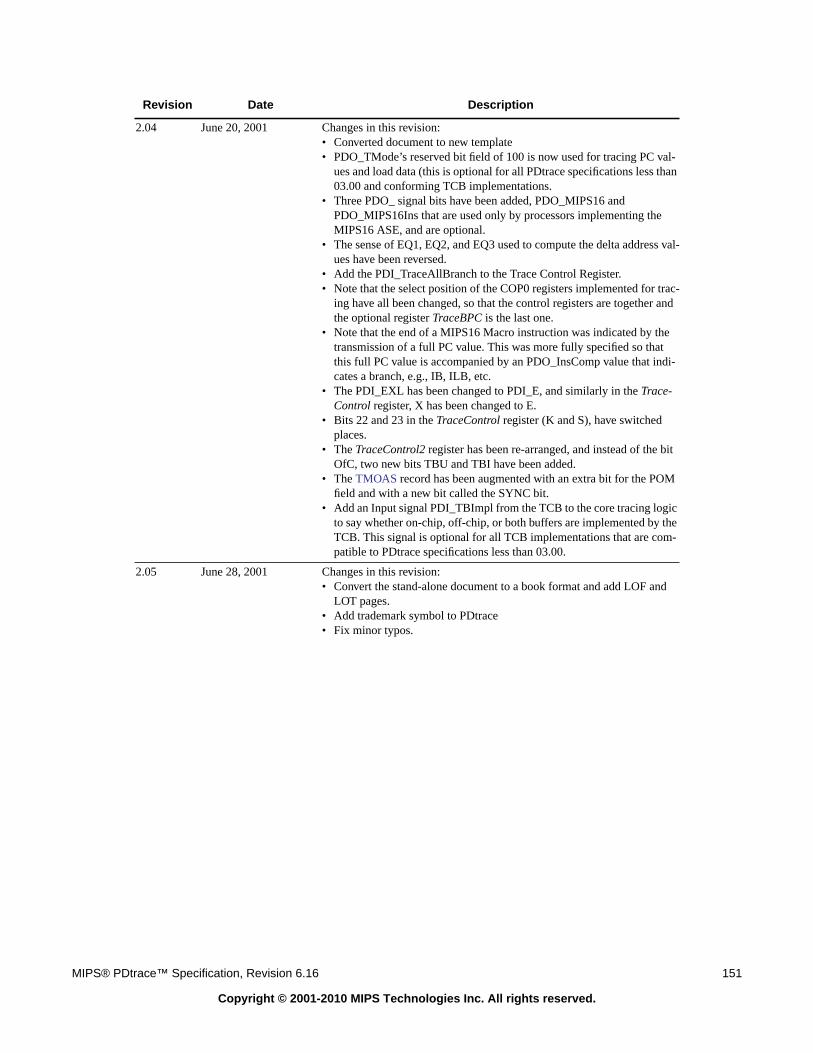
2.04 June 20, 2001 Changes in this revision:• Converted document to new template• PDO_TMode’s reserved bit field of 100 is now used for tracing PC val-
ues and load data (this is optional for all PDtrace specifications less than03.00 and conforming TCB implementations.
• Three PDO_ signal bits have been added, PDO_MIPS16 andPDO_MIPS16Ins that are used only by processors implementing theMIPS16 ASE, and are optional.
• The sense of EQ1, EQ2, and EQ3 used to compute the delta address val-ues have been reversed.
• Add the PDI_TraceAllBranch to the Trace Control Register.• Note that the select position of the COP0 registers implemented for trac-
ing have all been changed, so that the control registers are together andthe optional register TraceBPC is the last one.
• Note that the end of a MIPS16 Macro instruction was indicated by thetransmission of a full PC value. This was more fully specified so thatthis full PC value is accompanied by an PDO_InsComp value that indi-cates a branch, e.g., IB, ILB, etc.
• The PDI_EXL has been changed to PDI_E, and similarly in the Trace-Control register, X has been changed to E.
• Bits 22 and 23 in the TraceControl register (K and S), have switchedplaces.
• The TraceControl2 register has been re-arranged, and instead of the bitOfC, two new bits TBU and TBI have been added.
• The TMOAS record has been augmented with an extra bit for the POMfield and with a new bit called the SYNC bit.
• Add an Input signal PDI_TBImpl from the TCB to the core tracing logicto say whether on-chip, off-chip, or both buffers are implemented by theTCB. This signal is optional for all TCB implementations that are com-patible to PDtrace specifications less than 03.00.
2.05 June 28, 2001 Changes in this revision:• Convert the stand-alone document to a book format and add LOF and
LOT pages.• Add trademark symbol to PDtrace• Fix minor typos.
Revision Date Description
MIPS® PDtrace™ Specification, Revision 6.16 151
Copyright © 2001-2010 MIPS Technologies Inc. All rights reserved.

Revision History
2.06 August 8, 2001 Changes in this revision:• Define the behavior if the processor implements a fixed mapping MMU,
rather than the standard TLB-based MMU.• Define the polarity of the TraceControlASID_M field.
• Precisely define the processor modes which for which tracing may beenabled. See Section 2.2, "Processor Modes" on page 16 for these defi-nitions.
• Make the equations for turning on and off trace more precise and convertto standard notation.
• Add the standard “About This Book” chapter to define syntax and con-ventions.
• Eliminate the R/W fields in TraceControl2.• More fully describe the synchronization counter, including when it must
be restarted.• Make it explicit that ASID and processor mode changes are not traced if
tracing is off when the change occurs. That is, ASID and processormode changes are not traced if tracing is currently off.
• Add subsetting rules for PDtrace (see Section 2.3, "Subsetting" on page17)
• Add the PDO_ValidModes signal and the ValidModes field in theTraceControl2 register to specify which tracing modes the processorsupports.
2.07 March 21, 2002 Changes in this revision: (RT)• Change the name of the TraceControl2 register field ValidModes to
ImpSubset since this field indicated the implemented subset of tracing.• Get ready for commercial release, breakup the single file into individual
chapter files, fix typos, cross-references, etc.
3.00 November 26, 2002 Changes in this revision: (RT)• Change the way multi-issue tracing is done (see Section E.1,
"Background on High Performance Processors" on page 132).• Change the use of PDO_LoadOrder signal to PDO_DataOrder (see
Section E.4, "Out-of-Order Loads and Stores in the Multi-Pipe Core" onpage 135).
• Increase the width of PDO_DataOrder signal to 4 bits.• Add a new signal called PDO_DataPerIns[7:0].• Allow PDO_TEnd to be asserted early to cut off redundant upper bits of
an address or data.• Add a section to clarify how tracing is handled for store conditional
instructions (see Section 3.9, "Tracing Store Conditionals" on page 33).• Make the PDO_TMode bit 0 value for PDO_TType values of TD, TU1,
and TU2 to be Reserved.• Add PDO_Trig signals on the PDtrace interface that transmit trace trig-
ger information to the TCB. See Section 3.16, "Trace Trigger fromEJTAG Hardware Instruction/Data Breakpoints" on page 35.
• Add MIPS16 in MIPS64 option to ISAM in TMOAS. See Table 3.4 onpage 26.
• Rewrite the trace enable equation to fix errors in the first version. SeeSection 3.19, "Trace Enabling/Disabling Condition" on page 37.
• Fix grammatical errors and typos.
3.01 May 14, 2003 Removed the trace slot-specific signals PDO_TrigI_n, PDO_TrigD_n,PDO_TrigOn, and PDI_TrigOff, since these are superfluous. Fix minortypos.
Revision Date Description
152 MIPS® PDtrace™ Specification, Revision 6.16
Copyright © 2001-2010 MIPS Technologies Inc. All rights reserved.

4.10 July 4, 2005 Changes in this revision:• Merged the PDtrace and most of the TCB document• Modified how PDI_TraceMode works. This necessitated moving the
Mode bits from TraceControl to the TraceControl2 register.
• Simplified the SyncPeriod values to range from 25 to 212 for both typesof trace memory, on-chip or off-chip.
• Revamped how the EJTAG hardware breakpoint trigger impacts tracing.This has an impact on what used to be the TraceBPC control register.See spec for change details. Added the ability to trace based on a ARM-trace-DISARM feature, as well as to allow data qualified tracing.
• Added the ability to trace instruction and data cache misses• Added the ability to trace instructions that are potential function calls or
function returns.• Added support to trace multi-threaded processors that implement the
MIPS MT ASE.• Added a PendL, pending load field to the TMOAS record• Added a TCBControlC TCB register to deal with the added features
4.20 September 14, 2005 Changes include clarification of behavior under MT and removal of theMC bit in TCBControlB register.
4.30 January 30, 2006 Update the TMOAS record to add the V, DKill, and TCid fields for a MT-specific processor and remove a bad reference in chapter 7.
4.40 July 17, 2006 Change the drseg addresses of the TraceIBPC2 (0x1F28 to 0x1FF8) andTraceDBPC2 (0x2F28 to 0x2FF8) registers.
5.00 November 15, 2007 Significant change in the PDtrace architecture, the PDtrace interface is nolonger architecture and the only externally software-visible parts are thecontrol registers in CP0, in the TCB, and the TCB trace bits using thedefined TCB formats. Adds CMP support.
6.00 June 23, 2008 Add Performance counter support, Filtered data trace mode, and softwareaccess to on-chip trace memory. Expanded PEndL in TMOAS record.
6.10 November 06, 2008 Added 74K specific updates, on-chip trace memory updates for the 1004K
6.11 November 11, 2008 Added ability to start a TF at bit 56 if the Type15 continuation value is nototherwise needed
6.12 June 26, 2009 MIPS Technologies-only release for internal review:• LSB of TF3 may be optimized away for non-cycle-accurate mode• TCBTW register is writeable with predictable results
6.13 July 20, 2009 • Moved EJTAG trigger registers to their own chapter.• Moved Section on Memory map access of TCBRegisters from Chapter 2
to the TCB Register chapter.• Performance Counter Tracing now includes an optional additional cycle
counter.• Added section on how the On-Chip Trace Buffer is used.• For 1004K chapter, put in more description of the necessary control reg-
isters for on-chip trace buffer, e.g., TCBControlB.• More accurate description of how TCBSTP is affected by the TCBCon-
trolB.RM and TCBControlB.TR bits.• TF5 indicator is 4-bits again (previously widened to 5-bits in 4.00)
6.14 August 25, 2010 • Corrected definition of TF8.• Added Chapter for 1074K with description of TraceMaster TAP control-
ler.• Clarifications for when PC Tracing is disabled.
Revision Date Description
MIPS® PDtrace™ Specification, Revision 6.16 153
Copyright © 2001-2010 MIPS Technologies Inc. All rights reserved.

Revision History
6.15 September 07 2010 • Explicitly list which registers are affected by TRPAD bit.• TRPAD bit in TraceControl3 is read-only. TCBControlB descriptions
were incorrect.• Rearrange chapters to put more basic topics at the beginning of docu-
ment.• Pulled in tech writers’ english grammer/syntax edits.
6.16 November 23, 2010 • Move 1074K Appendix content to CMP Appendix - Trace-Masteraccess method now shared with 1004K product line.
Revision Date Description
154 MIPS® PDtrace™ Specification, Revision 6.16
Copyright © 2001-2010 MIPS Technologies Inc. All rights reserved.