mil-std-883h - massachusetts institute of technology · mil-std-883h method 5010.4 18 june 2004 1...
TRANSCRIPT
MIL-STD-883H
METHOD 5010.4 18 June 2004
1
METHOD 5010.4
TEST PROCEDURES FOR COMPLEX MONOLITHIC MICROCIRCUITS
1. PURPOSE. This method establishes screening, qualification, and quality conformance requirements for the testing of complex monolithic microcircuits to assist in achieving the following levels of quality (class level B and S) and reliability commensurate with the intended application. Complex monolithic microcircuits are defined as monolithic devices that contain a minimum of 4,500 transistors. It shall be used in conjunction with other documentation such as appendix A of MIL-PRF-38535 and an applicable device specification or drawing to establish the design, material, performance, control, and documentation requirements which are needed to achieve prescribed levels of device quality and reliability.
2. APPARATUS. Suitable measurement equipments necessary to determine compliance with applicable acquisition documents and other apparatus as required in the referenced test methods. 3. PROCEDURE. The procedures defined herein, including appendix I and II, outline the requirements and testing necessary to certify and qualify a complex microcircuit design, fabrication, assembly and testing facility. It illustrates the concept of generic qualification through the use of standard evaluation circuits and process monitors.
3.1 Test procedures for complex monolithic microcircuits. Complex monolithic microcircuits shall be tested as described herein, and in the device specification or drawing.
3.1.1 Precedence. Unless otherwise specified in the device specification or drawing, the test requirements and conditions shall be given herein.
3.1.2 Electrostatic discharge sensitivity. Electrostatic discharge sensitivity testing, marking, and handling shall be in accordance with appendix A of MIL-PRF-38535.
3.1.3 Failure analysis. When required by the applicable device specification failure analysis of devices rejected during any test in the screening sequence shall be accomplished in accordance with method 5003, test condition A.
3.1.4 Failure analysis class level S. Class level S devices shall be analyzed in accordance with method 5003, test condition B to identify the cause for failed lots and burn-in failures in accordance with appendix A of MIL-PRF-38535, A.4.3.3.1, and A.4.6.1.2.1. The documented results shall only be reported to the qualifying or acquiring activity when specifically requested.
3.1.5 Class requirements. Within tables having a class column, only those test and inspections or subgroups identified with "B" are applicable to class level B. All apply to class level S.
3.1.6 Radiation. When required by the applicable device specification or drawing, qualification, and quality conformance inspection requirements for radiation hardness assured devices are in addition to the normal class level S and B requirements. These requirements for each specified radiation levels (M, D, P, L, R, F, G and H) are detailed in table VIII herein.
3.2 Element evaluation.
3.2.1 General.
3.2.1.1 Element. Herein "element" refers to materials for device assembly. Before device assembly, element characteristics shall be evaluated and verified to assure their compatibility with element specifications, device requirements, and manufacturing procedures (see table I). Also, characteristics which cannot be verified after manufacturing but could cause function failure shall be evaluated and verified before assembly.

MIL-STD-883H
METHOD 5010.4 18 June 2004
2
TABLE I. Element evaluation summary.
Element Paragraph Requirement
Microcircuit wafer 3.2.2 Appendix II (herein)
Package 3.2.3 Table II (herein)
3.2.1.2 Element evaluation requirements. Element evaluation may be performed at either the element supplier or device manufacturing facility up to the point where the element must undergo processing or assembly prior to testing. If element evaluation is performed by the supplier, then the device manufacturer must obtain a summary of the results for verification, and record retention.
3.2.2 Microcircuit wafer evaluation.
3.2.2.1 Definition. Diffused wafers used and evaluated shall, as a minimum, be complete with interconnect layers and glassivation from material that was homogeneously processed through wafer fabrication.
3.2.2.2 General. For the purpose of microcircuit wafer evaluation and wafer lot acceptance, measurement of the process monitor (PM), verifying that the identified parameters are within process limits, will be required from each wafer lot in accordance with appendix II wafer lot acceptance herein. Each die from each diffused wafer lot shall be electrically tested prior to assembly in accordance with the manufacturer's in-house documentation.
3.2.3 Package evaluation. Each package type shall be evaluated and characterized in accordance with table II herein prior to use. Finite element analyses techniques may be used. Packages used for complex monolithic microcircuits and fabricated to this test method shall be tested as follows:
3.2.3.1 Definition. Package used and evaluated shall consist of the same element specifications, materials, and finish; and homogeneously processed through device assembly.
3.2.3.2 Incoming inspection.
a. From the initial package inspection lot, a randomly selected sample shall be subjected to package evaluation (see table II). Additionally, subgroup 3 testing shall be accomplished using sealed packages. A die may be attached. Subgroups 2, 3, and 4 apply to cases only.
b. Additionally, subgroups 1, 2, and 3 of table II shall be accomplished for each subsequent acquisition.
c. For solderability (subgroup 2), lead integrity (subgroup 3), and metal package isolation (subgroup 4) defined within
table II, a quantity (accept number) of 15 (0) shall apply to the number of terminals or leads tested. The leads shall be randomly selected from the three packages.

MIL-STD-883H
METHOD 5010.4 18 June 2004
3
TABLE II. Package evaluation requirements.
Subgroup Class levels Test MIL-STD-883 Quantity (accept number)
Reference paragraph
S B Method Condition
1 X X Physical dimensions 2016 15 (0) 3.2.3.3
2 X X Solderability 2003 Solderability temperature 245 5°C
3 (0) 1/
3 X X Thermal shock or Temperature cycle
1011 1010
C C (20 cycles)
3 (0)
X X High temperature bake 1008 2 hours at 150°C
3 (0)
X X Lead integrity 2004 2028
B2 (lead fatigue) D (leadless chip carriers) B1 (leaded chip carrier packages) (Pin grid array leads and rigid leads)
3 (0) 1/
X X Seal 1014 D Sealed cases
3 (0)
4 X X Metal package isolation
1003 600 V dc, 100 nA maximum
3 (0) 1/
3.2.3.4
5 X X Insulation 1003 2/ 3 (0)
6 X X Conductor MIL-STD- 202 method 307
2/ 3 (0)
7 X X Thermal characterization
1012 3/
1/ A quantity (accept number) of 15 (0) shall apply to the number of terminals or leads to be tested. The leads
shall be randomly selected from three packages minimum. 2/ Selected from three packages minimum. Conditions as specified by acquisition document and Appendix A of
MIL-PRF-38535. 3/ Required on all package types prior to initial use.
MIL-STD-883H
METHOD 5010.4 18 June 2004
4
3.2.3.3 Subgroup 1. Separately verify case and cover dimensional compliance with the device specification or drawing.
3.2.3.4 Subgroup 4. For metal cases with leads separated by an insulator, measure insulation resistance between the
metal body of the case and the leads that are isolated from the case. This test does not apply to nonmetallic cases. 3.3 Manufacturing control.
3.3.1 Process control requirements. Line control as detailed below is required. 3.3.1.1 Wafer fabrication controls. Wafer fabrication shall be controlled in accordance with the manufacturer's fabrication baseline and documented procedures of the fabrication process.
3.3.1.2 Assembly controls. Assembly controls shall be in accordance with the manufacturer's assembly baseline and documented assembly procedures and additions herein
3.3.2 Design/layout system control. Design/layout controls shall be implemented using appendix I as a guide.
3.3.3 Testing controls. Documentation of testing controls shall meet the requirements of MIL-PRF-38535, appendix A.
3.3.3.1 Test vectors. The manufacturing-level logic test vectors shall be graded for fault coverage using a fault simulator. The resulting fault coverage shall be reported in the device specification or drawing. Fault coverage shall be based on the detectable equivalence classes of single, permanent, stuck at zero, and stuck at one faults on all logic lines of a structural logic model. The logic model shall be expressed in terms of gate-level primitives or simple atomic functions (such as flip-flops). Large, regular structures such as RAMs and ROMs shall not be modeled at the gate level; rather, documentation shall be provided to show that these structures are tested using appropriate procedures (such as, galloping patterns for a RAM).
3.3.3.2 Built-in-test/build-in-redundancy. When specified in the device specification or drawing, the following shall apply.
3.3.3.2.1 Probe/bond sites. The device shall contain probe/bond sites to allow testing using the full set of test vectors specified in the device specification or drawing.
3.3.3.2.2 Built-in redundancy for yield enhancement. Where built-in redundancy is used to provide yield enhancement, testing shall be included to provide a statistic which represents the amount of alternate element selection utilized.
3.3.3.2.3 Built-in redundancy using self test and fix. Where built-in redundancy is provided in the form of self test and fix, the circuitry will be capable of interrogation to determine the level of redundancy remaining on the device.
3.3.4 Quality controls. The product assurance program plan shall be in accordance with MIL-PRF-38535, appendix A.
3.3.4.1 Process monitor. Process control and stability of dc parameters must be demonstrated through the use of the manufacturer's process monitor (PM). The PM is to be designed so that the dc process parameters may be measured in wafer form. The PM may also be packaged so as to permit biasing of those circuits for measurement. The PM design must be submitted to the qualifying activity for approval prior to qualification and must contain as a minimum the structures outlined in table I of appendix II herein.

MIL-STD-883H
METHOD 5010.4 18 June 2004
5
3.3.4.1.1 Process monitors for other technology devices. An adequate set of PM's applicable for other technology
devices shall be generated to assure that applicable failure mechanisms are detected and submitted for approval by the qualifying activity.
3.3.4.2 Qualification device. A qualification device shall be used to demonstrate process stability and reliability. The qualification device, either a standard evaluation circuit (SEC) or an actual device (worst case design) shall be submitted to the qualifying activity for approval and as such contain the basic information as detailed herein. The qualification device shall be fabricated with the same process and designed to the same design rules that will produce any device in the technology to be qualified. The qualification device design shall be configured in such a manner so as to evaluate the reliability of the underlayer designs (e.g., diffusion) and evaluate the worst case design rule conditions on the personalization layers. The design should utilize cell libraries as well as test structures which will detect metal to metal shorting or opening, high via resistance and dielectric pinholes during reliability life testing, where applicable. The following structures are suggested:
Parameter Structure
Functionality and performance Large functional block (ALU), ring oscillator
Contact resistance/electromigration Contact strings Hot electrons/holes Short channel devices Oxide breakdown voltage Capacitors Resistance (electromigration test) Metal stripes
3.4 Screening procedures for microcircuits. Screening of microcircuits shall be conducted as described in 3.4 through
3.4.13 and table III herein. This provision does not preclude the performance of additional tests or inspection which may be required for specific devices or which may be desirable to optimize results of screening; however, any such special test inspection shall be subjected to the requirements of appendix A of MIL-PRF-38535, A.4.3.4 and A.4.3.7. Sampling inspections shall not be an acceptable substitute for any specified screening test. Any burn-in, in addition to that specified, is only permitted when documented in the lot records, and any failures shall be counted in applicable PDA calculations. Where end point or post test measurements are required as part of any given test method used in the screening procedure and where such post-test measurements are duplicated in the interim (post burn-in) or final electrical tests that follow, such measurements need not be duplicated and need to be performed only as part of the interim (post burn-in) or final electrical tests. Devices which pass screening requirements of a higher reliability level shall be considered to meet the screening requirements of all lower levels. In no case shall screening to a lower level than that specified be permitted.
3.4.1 General.
a. Devices that fail any test or inspection criteria in the screening sequence shall be removed from the lot at the time of observation or immediately at the conclusion of the test in which the failure was observed. Once rejected and verified as a device failure, no device may be retested for acceptance. Unless otherwise specified in the device specification or drawings, electrical rejects may be used to satisfy sample selection requirements for qualification and quality conformance inspection in accordance with 3.5.
b. Device screening shall be performed in the sequence shown in table III except where variations in sequence are
specifically allowed herein.

MIL-STD-883H
METHOD 5010.4 18 June 2004
6
TABLE III. Device screening.
Screen Class level S Class level B Reference paragraph
Method Reqmt Method Reqmt
Wafer lot acceptance 5010 appendix II and 5007
All lots
5010 appendix II All lots
Nondestructive bond pull 2023 100%
Internal visual 2010, test condition A
100% 2010, test condition B
100% 3.4.2
Stabilization bake. No end point measurements required
3.4.3
Temperature cycling or thermal shock
1010, test condition C
100% 1010, test condition C 1011, test condition A
100% 100%
3.4.5
Constant acceleration 2001, test condition E (min) Y1 orientation only
100% 2001, test condition E (min) Y1 orientation only
100% 3.4.6
Visual inspection 100% 100%
Particle impact noise detection (PIND)
2020, test condition A
100% 3.4.7
Serialization 100%
Interim (pre-burn-in) electrical parameters
In accordance with applicable device specification
100% In accordance with applicable device specification
100% 3.4.9.1
Burn-in test 1015 240 hours at 125°C minimum
100% 1015 160 hours at 125°C minimum
100% 3.4.10
Interim (post-burn-in) electrical parameters
In accordance with applicable device specification
100% Optional 3.4.9.1
Reverse bias burn-in 1015; test condition A or C, 72 hours at 150° minimum.
100%

MIL-STD-883H
METHOD 5010.4 18 June 2004
7
TABLE III. Device screening -Continued.
Screen Class level S Class level B Reference paragraph
Method Reqmt. Method Reqmt.
Interim (post-burn-in) electrical parameters
In accordance with applicable device specification
100% In accordance with applicable device specification
100% 3.4.9.1
Percent defective allowable (PDA) calculation
5 percent (subgroup 1, table IV) 3 percent functional parameters at 25°C (subgroup 7 table IV)
All lots
5 percent (subgroup 1, table IV)
All lots
3.4.9.1
Final electrical test a. Static tests (1) 25°C (subgroup 1, table IV) (2) Maximum and minimum rated operating temp. (subgroup 2, 3, (table IV) b. Dynamic or functional tests (1) 25°C (subgroup 4, or 7, table IV) (2) Minimum and maximum rated operating temp. (subgroup 5 and 6, or 8, table IV) c. Switching tests at 25°C (subgroup 9,) table IV)
In accordance with applicable device specification
100% 100% 100% 100% 100%
In accordance with applicable device specification
100% 100% 100% 100% 100%
3.4.11

MIL-STD-883H
METHOD 5010.4 18 June 2004
8
TABLE III. Device screening - Continued.
Screen Class level S Class level B Reference paragraph
Method Reqmt. Method Reqmt.
Seal Fine Gross
1014 100% 1014 100% 3.4.8
Radiographic 2012 two views 100% 3.4.12
Qualification or quality conformance inspection test sample selection
See 3.5 See 3.5
External visual 2009 100% 2009 100% 3.4.13
3.4.2 Internal visual inspection. Internal visual inspection shall be performed to the requirements of method 2010,
condition A for class level S devices and condition B for class level B devices. Devices awaiting preseal inspection, or other accepted, unsealed devices awaiting further processing shall be stored in a dry, inert, controlled environment until sealed. Unless otherwise specified, at the manufacturer's option, test samples for group B, bond strength may be randomly selected prior to or following internal visual, prior to sealing provided all other specification requirements are satisfied (e.g., bond strength requirements shall apply to each inspection lot, bond failures shall be counted even if the bond would have failed internal visual exam). The alternate procedure of 3.4.2.1 shall be used when any of the following criteria are met:
a. Minimum horizontal geometry is less than three microns.
b. Metallization consists of two or more levels.
c. Opaque materials mask design features.
3.4.2.1 Alternate procedures for class level B microcircuits. Alternate procedures may be used on an optional basis on any microcircuit, provided that the conditions and limits of the alternate procedures are submitted to, and approved by the preparing activity, or the acquiring activity.
3.4.2.1.1 Alternate procedures. The deletions and the changes stated herein are allowable only if the requirements of alternate 1 or alternate 2 are met.
Alternate 1: The deletions and the changes stated in 3.4.2.1.1a. are allowable for complex monolithic microcircuits for class level B product only if the requirements of 3.4.2.1.1.b and 3.4.2.1.1.c are imposed and any of the following conditions exists.
1. Minimum horizontal geometry is less than 3 micrometers (m). 2. Interconnects consisting of two or more levels. 3. Opaque materials mask design features.
a. For inspection of each microcircuit die, delete the inspection criteria of 3.1.1, 3.1.2, 3.1.3, 3.1.4, 3.1.5, 3.1.6, 3.1.7, and 3.2.5 of condition B of method 2010 and for use in conjunction with alternate procedures, add 3.1.1.1, 3.1.1.2, 3.1.1.6, 3.1.3, 3.1.4, and 3.2.5 to the low magnification inspection of method 2010.
b. Temperature cycling (3.4.5). The minimum total number of temperature cycles shall be 50. The manufacturer
may reduce the number of temperature cycles from 50 to the 10 required as part of normal screening based upon data justifying the reduction in temperature cycles approved by the preparing activity and an approved plan which shall include the following criteria:

MIL-STD-883H
METHOD 5010.4 18 June 2004
9
(1) Reduction of test must be considered separately for each wafer fabrication line and each die family. (2) The manufacturer shall demonstrate that the wafer fabrication line that produces product which will involve
reduction of temperature cycles is capable and in process control. (3) The manufacturer shall perform a high magnification visual inspection on a small sample of devices (e.g.,
5(0)) to monitor the process. This inspection may be performed at wafer level.
c. Special electrical screening tests shall be applied to each microcircuit die at the wafer, individual die (chip) and packaged, or both, microcircuit level in accordance with the requirements of MIL-STD-883, method 5004, 3.3.2. The conditions and limits of the electrical tests (in table III format) shall be submitted to the preparing activity for approval and subsequently maintained on file with the qualifying activity. These special screens are in addition to the required electrical parametric tests which the device must pass and shall be designed to screen out devices with defects that were not inspected to the full criteria of 3.4.3 (internal visual). Due to the nature of these tests, they are not to be repeated as part of the qualification and quality conformance procedures.
Alternate 2: The requirements and conditions for use of this alternate are contained in appendix A of method
5004. This option applies to both class level B and class level S microcircuits.
3.4.3 Stabilization bake. Stabilization bake is not required for class level S or class level B product unless specified in the device specification or drawing.
3.4.4 Visual inspection for damage. The manufacturer may inspect for damage after each screening step. Damaged devices shall be removed from the lot.
3.4.5 Temperature cycling or thermal shock. All devices shall be subjected to the requirements of temperature cycling or thermal shock. The device specifications or drawing shall specify which screen shall be employed. Temperature cycling shall be in accordance with MIL-STD-883, method 1010, condition C minimum. For class level B, this test may be replaced with thermal shock in accordance with MIL-STD- 883, method 1011, condition A minimum.
3.4.6 Constant acceleration. All devices shall be subjected to constant acceleration, in the Y1 axis only, in accordance with MIL-STD-883, method 2001, condition E (minimum). Microcircuits which are contained in packages which have an inner seal or cavity perimeter of two inches or more in total length or have a package mass of five grams or more may be treated in accordance with provisions below as an alternate to this procedure. Delete test condition E and replace with test condition D. Unless otherwise specified, the stress level for large, monolithic microcircuit packages shall not be reduced below condition D. If the stress level specified is below condition D, the manufacture shall have data to justify this reduction and this data must be maintained and available for review by the preparing or acquiring activity. The minimum stress level allowed is condition A.
3.4.7 Particle impact noise detection test (PIND). Testing to be performed in accordance with appendix A of MIL-PRF-38535, A.4.6.3. The PIND test may be performed in any sequence after temperature cycling and prior to final electrical test.
3.4.8 Seal (fine and gross leak) testing. For class level S devices seal testing may be performed in any sequence between the final electrical test and external visual, but it shall be performed after all shearing and forming operations on the terminals. For class level B devices, fine and gross seal test shall be performed separate or together in any sequence and order between 3.4.7 and 3.4.13 and they shall be performed after all shearing and forming operations on the terminals. When the 100 percent seal screen cannot be performed following all shearing or forming operations (i.e., flat packs, brazed lead packages, and chip carriers) the seal screen shall be done 100 percent prior to those shearing and forming operations and a sample test using sample size number of 45 (C = 0) shall be performed on each inspection lot following these operations to verify integrity. For devices with leads that are not glass-sealed and that have a lead pitch less than or equal to 1.27 mm (0.050 inch), the sample seal test shall be performed using an acceptance criteria of a quantity (accept number) of 15 (0). If sample fails the sample acceptance criteria, all devices in the inspection lot represented by the sample tested shall be subjected to and pass 100 percent fine and gross leak seal screens.

MIL-STD-883H
METHOD 5010.4 18 June 2004
10
3.4.9 Electrical measurements.
3.4.9.1 Interim (pre- and post-burn-in) electrical parameters. Interim (pre- and post-burn-in) electrical testing shall be
performed when specified, to remove defective devices prior to further testing or to provide a basis for application of percent defective allowable (PDA) criteria when a PDA is specified. The PDA shall be 5 percent or one device, whichever is greater. This PDA shall be based, as a minimum, on failures from group A, subgroup 1 plus deltas (in cases where delta parameters are specified) with the parameters, deltas, and any additional subgroups (or subgroups tested in lieu of A-1) subject to the PDA as specified in the applicable device specification or drawing. If no device specification or drawing exists, subgroups tested shall at least meet those of the most similar device specification or Standard Microcircuit Drawing. In addition, for class level S the PDA shall be 3 percent (or one device, whichever is greater) based on failures from functional parameters measured at room temperature. For class level S screening, where an additional reverse bias burn-in is required, the PDA shall be based on the results of both burn-in tests combined. The verified failures after burn-in divided by the total number of devices submitted in the lot or sublot for burn-in shall be used to determine the percent defective for that lot, or sublot and the lot or sublot shall be accepted or rejected based on the PDA for the applicable device class. Lots and sublots may be resubmitted for burn-in one time only and may be resubmitted only when the percent defective does not exceed twice the specified PDA, or 20 percent, whichever is greater.
3.4.9.2 Pattern failures. Pattern failure criteria may be used as an option for class level B, provided that:
a. Inspection lot size is less than 500 devices. b. Pre burn-in electrical testing is done.
3.4.9.2.1 Pattern failures criteria. A maximum number of pattern failures (failures of the same part type when the failures
are caused by the same basic failure mechanism) shall apply as specified in the acquisition document. If not otherwise specified, the maximum allowable pattern failures shall be five. Accountability shall include burn-in through final electrical test.
3.4.9.2.2 Pattern failure resubmission. When the number of pattern failures exceeds the specified limits, the inspection lot shall be rejected. At the manufacturer's option, the rejected lot may be resubmitted to burn-in one time provided:
a. The cause of the failure has been evaluated and determined.
b. Appropriate and effective corrective action has been completed to reject all devices affected by the failure cause.
c. Appropriate preventive action has been initiated.
3.4.10 Burn-in. Device burn-in shall be performed in accordance with the requirements of method 1015 conditions A, B, C, D, or E. Regardless of power level, devices shall be able to be burned-in at their maximum rated operating temperature. For devices whose maximum operating temperature is stated in terms of ambient temperature, TA, table I of method 1015 applies. For devices whose maximum operating temperature is stated in terms of case temperature, TC, and where the ambient temperature would cause TJ to exceed 200C for class level B or 175°C for class level S, the ambient operating temperature may be reduced during burn-in from 125°C to a value that will demonstrate a TJ between 175°C and 200°C (for both class levels S and B) and TC equal to or greater than 125°C without changing the test duration. Data supporting this reduction shall be available to the acquiring and qualifying activities upon request.
3.4.11 Final electrical measurements. Final electrical testing of microcircuits shall assure that the microcircuits tested meet the electrical requirements of the applicable device specification or drawing and shall include, as a minimum, the tests of group A, subgroups 1, 2, 3, 4 or 7, 5 and 6, or 8, and 9.
3.4.12 Radiographic. The radiographic screen may be performed in any sequence after PIND test and before external visual inspection. Only one view is required for flat packages and leadless chip carriers having lead (terminal) metal on four sides. 3.4.13 External visual inspection. All devices shall be inspected in accordance with MIL-STD-883, method 2009, prior to acceptance for shipment

MIL-STD-883H
METHOD 5010.4 18 June 2004
11
3.5 Qualification and quality conformance procedures. Qualification and quality conformance shall be performed in accordance with A.4.4 qualification procedures and A.4.5 quality conformance inspection of appendix A of MIL-PRF-38535 except as modified herein. The qualification device shall be used for QCI testing in accordance with 3.5.3 herein, as well as for qualifying the process line. Life testing requirements shall follow the same criteria as burn-in (3.4.10 herein) for reduced temperature.
3.5.1 Qualification testing. Initial product process qualification shall be in accordance with MIL-STD-883 method 5005. Change to qualified product shall be addressed in accordance with MIL-STD-883, method 5005 and appendix A of MIL-PRF-38535, A.3.4.2. The SEC shall be used for group D inspection whenever practical; where the SEC cannot be used, another die may be used (for gate arrays, 60 percent or greater utilization required). Utilizing the qualification device the process monitor, the manufacturer shall demonstrate:
a. Process control and stability.
b. Process/device reliability.
c. Design and simulation control.
3.5.1.1 Detailed qualification test plan. The manufacturer shall submit to the qualifying activity for approval a detailed qualification test plan to assure conformance to 3.5.1 herein. The test plan shall, as a minimum, define test groups, subgroups, conditions, and sampling plans in accordance with method 5005, as well as the tests to carry out 3.5.1.2, 3.5.1.3, and 3.5.1.4.
3.5.1.2 Database test. For qualification, at least five PM's per wafer (located in accordance with appendix II) shall be measured to ensure the establishment of a statistically valid database on which a decision can be made as to whether the manufacturer's process is stable and under control.
3.5.1.3 Qualification device design and test plan. Qualification device design and test plan to be used to qualify the manufacturing line shall be submitted to the qualifying activity for approval. The design must meet the minimum requirements of 3.3.4.2 herein. The test plan must include life test requirements. If a SEC is used as the qualification device, data demonstrating process reliability from lots processed within 12 months of qualification and that an on-going SEC program is in effect shall be submitted for qualifying activity review.
3.5.1.4 Design and simulation verification. Design and simulation verification shall be accomplished as follows:
a. Design rule check (DRC) verification. DRC software shall be run on a design which contains known design rule violations.
b. Electrical rule check (ERC) verification. ERC software shall be run on a design which contains known electrical
rule violations (e.g., fan-out violations).
c. Layout versus schematic (LVS) check.
d. Correct by construction. If the manufacturers' design methodology is based on a "correct by construction" approach, distinct DRC, ERC, and LVS software is unnecessary and a, b, and c above do not apply. However, the manufacturer shall provide suitable data to demonstrate the correct performance of "correct by construction" software.
e. Computer aided design (CAD) system control shall be in accordance with appendix I herein.
3.5.2 Quality conformance inspection. This procedure, as applicable to the microcircuit type and class, shall apply for all
quality conformance inspection requirements. Subgroups within a group of tests may be performed in any sequence but individual tests within a subgroup (except group B, subgroup 2) shall be performed in the sequence indicated for groups B, C, D, and E tests herein. Where end-point electrical measurements are required for subgroups in groups B, C, D, and E testing herein, they shall be as specified in the applicable device specification or drawing. Where end-point measurements are required but no parameters have been identified in the acquisition document for this purpose, the final electrical parameters specified for 100 percent screening shall be used as end-point measurements. Electrical reject devices from the same inspection lot may be used for all subgroups when end-point measurements are not required.
3.5.2.1 Radiation hardness. Quality conformance inspection requirements for radiation hardness assured devices are in addition to the normal class level S and B requirements. Those requirements are detailed in table VIII (group E) herein. The radiation levels (M, D, P, L, R, F, G and H) are defined in appendix A of MIL-PRF-38535.

MIL-STD-883H
METHOD 5010.4 18 June 2004
12
3.5.2.2 Quality conformance inspection. For class level B quality conformance inspection, each inspection lot (sublot) shall pass groups A, B, and E (when applicable) tests or be accepted in accordance with 3.5.3 herein and the periodic group C and D tests shall be in accordance with appendix A of MIL-PRF-38535. End point electrical parameters shall be as specified in 3.5.2.3 herein. For class level S, each QCI inspection lot shall be assembled in accordance with the class level S requirements of appendix A of MIL-PRF-38535. Quality conformance testing for class level S shall be in accordance with tables IV, V, VI, and VII herein.
3.5.2.3 End point electrical parameters. Where intermediate and end point electrical measurements are required for subgroups B, C, D, and E testing, they shall be as specified in the applicable device specification or drawing where required and when end point parameters have not been identified, group A, subgroup 1, 2, 3, 4 or 7, and 9 shall be used for end point measurements. 3.5.2.4 Constant acceleration. Constant acceleration shall be performed in accordance with method 2001, test condition E for all applicable subgroups except as allowed in accordance with 3.4.6, herein. 3.5.3 Quality conformance testing. Conformance testing shall be performed through the use of the identified quality conformance vehicles. Quality conformance test Quality conformance vehicle Frequency Table IV Group A Actual device Each inspection lot Table V Group B Actual device Each inspection lot Table VI Group C SEC or actual device 3 months Table VII Group D SEC or actual device 6 months
Table VIII Group E Actual device See MIL-PRF-38535. appendix A 3.5.3.1 Alternate group A method. The alternate group A method below may be used provided that:
a. Inspection lot size is less than 500 devices.
b. Final electrical test shall assure that the electrical requirements of the device specification or drawing are met and shall include the tests of group A, subgroups 1, 2, 3, 4 or 7, 5 and 6 or 8, 9, as a minimum.
c. All test software and procedures are under document control.
3.5.3.1.1 In-line verification testing.
a. For each test set up (and operator for manual testing), production runs correlation unit to assure that the accuracy requirements of MIL-STD-883 4.5.2 are being met.
b. Testing is performed using the verified set up. c. At the completion of testing utilizing the verified set up (not to exceed 8 hours and at the change of operators) a
separate party (QA or QA designate) then verifies the production testing by:
(1) Checking visually to verify that the correct fixture, equipment, software, and procedure(s) were used. (2) Actual testing of controlled known good device utilizing the fixtures, set ups, software and procedures that
were used by production. Variables data for all required group A tests shall be read and recorded for the controlled unit. This data shall be maintained with the lot.
MIL-STD-883H
METHOD 5010.4 18 June 2004
13
TABLE IV. Group A electrical test. 1/
Subgroup Parameters 2/ 3/ 4/ 5/ Quantity/ acceptance number
1 Static test at +25C 116/0
2 Static tests at maximum rated operating temperature 116/0
3 Static tests at minimum rated operating temperature 116/0
4 Dynamic test at +25C 116/0
5 Dynamic tests at maximum rated operating temperature 116/0
6 Dynamic tests at minimum rated operating temperature 116/0
7 Functional test at +25C 116/0
8 Functional tests at maximum and minimum rated 116/0 operating temperatures
9 Switching tests at +25C 116/0
10 Switching tests at maximum rated operating temperature 116/0
11 Switching tests at minimum rated operating temperature 116/0
1/ The specific parameters to be included for tests in each subgroup shall be as specified in the applicable acquisition
document. Where no parameters have been identified in a particular subgroup or test within a subgroup, no group A testing is required for that subgroup or test to satisfy group A requirements.
2/ At the manufacturer's option, the applicable tests required for group A testing (see 1/) may be conducted individually or combined into sets of tests, subgroups (as defined in table I), or sets of subgroups. However, the manufacturer shall predesignate these groupings prior to group A testing. Unless otherwise specified, the individual tests, subgroups, or sets of tests/subgroups may be performed in any sequence.
3/ The sample plan (quantity and accept number) for each test, subgroup, or set of tests/subgroups as predesignated in 2/ above, shall be 116/0.
4/ A greater sample size may be used at the manufacturer's option; however, the accept number shall remain at zero. When the (sub)lot size is less than the required sample size, each and every device in the (sub)lot shall be inspected and all failed devices removed from the (sub)lot for final acceptance of that test, subgroup, or set of tests/subgroups, as applicable.
5/ If any device in the sample fails any parameter in the test, subgroup, or set of tests/subgroups being sampled, each and every additional device in the (sub)lot represented by the sample shall be tested on the same test set-up for all parameters in that test, subgroup, or set of tests/subgroups for which the sample was selected, and all failed devices shall be removed from the (sub)lot for final acceptance of that test, subgroup, or set of tests/subgroups, as applicable. For class level S only, if this testing results in a percent defective greater than 5 percent, the (sub)lot shall be rejected, except that for (sub)lots previously unscreened to the tests that caused failure of this percent defective, the (sub)lot may be accepted by resubmission and passing the failed individual tests, subgroups, or set of tests/subgroups, as applicable, using a 116/0 sample.

MIL-STD-883H
METHOD 5010.4 18 June 2004
14
TABLE V. Group B testing.
Subgroup Class level
Test
MIL-STD-883 quantity/(accept
number) or sample
size number, accept number
Referenced paragraph
S B Method Condition
1
X X Physical dimensions 2016 2 (0)
2 X Particle impact noise detection test
2020 A or B 15 (0) 3.4.7
3 X X Resistance to solvents 2015 3 (0)
4 X X Internal visual and mechanical
2014 1 (0) 3.4.2
5 X X Bond strength a. Thermocompression b. Ultrasonic or wedge c. Flip-chip d. Beam lead
2011 C or D C or D F H
2 (0)
6 X X Die shear strength or substrate attach strength
2019 or 2027
2 (0)
7 X X Solderability 2003 Solder temperature 245C 5C
1 (0)
8 X X Seal a. Fine b. Gross
1014 Sample size number = 15 C = 0
3.4.8

MIL-STD-883H
METHOD 5010.4 18 June 2004
15
TABLE VI. Group C testing.
Subgroup Class levels
Test MIL-STD-883 Sample size number,
accept number
Referenced paragraph
S B Method Condition
1 X X X X X X X
X X X X X X
External Temperature cycling Mechanical shock or constant acceleration Seal (fine and gross) Radiographic Visual examination End point electrical
2009 1010 2002 2001 1014 2012
C 100 cycles minimum B, Y1 axis E, Y1 axis Y axis In accordance with visual criteria of method 1010. As specified in accordance with device specification
Sample size number = 15 C = 0
3.4.13 3.4.5 3.4.6 3.4.8 3.4.12 3.5.2.3
2 X X Steady-state life test End point electrical
1005 1,000 hours at +125°C minimum As specified in accordance with device specification
Sample size number = 22 C = 0
3.5.2.3
TABLE VII. Group D testing.
Subgroup Class Test
MIL-STD-883 Quantity/
accept number
Referenced paragraph
S B Method Condition
1 X X Internal water vapor content 5000 PPM maximum water content at +100°C
1018 3 devices (0 failures) or 5 devices (1 failure)
2 X X Moisture resistance 1004 5 (0)
3 X X Salt atmosphere 1009 5 (0)

MIL-STD-883H
METHOD 5010.4 18 June 2004
16
TABLE VIII. Group E (radiation hardness assurance tests). 1/
Test MIL-STD-883 Class level S Class level B
Method Condition Quantity/ accept number
Notes
Quantity/ accept
number
Notes
Subgroup 1 2/ Neutron irradiation a. Qualification b. QCI Endpoint electrical parameters
1017
+25°C As specified in accordance with device specification
a. 11 (0) b. 11 (0)
3/ 3/
a. 11 (0) b. 11 (0)
4/ 4/
Subgroup 2 5/ Steady-state total dose irradiation a. Qualification b. QCI Endpoint electrical parameters
1019
+25°C Maximum supply voltage As specified in accordance with device specification
a. 4 (0) 2 (0) b. 4 (0) 2 (0)
a. 6/ 8/ b. 6/ 8/
a. 22 (0) b. 22 (0)
7/ 7/
1/ Parts used for one subgroup test may not be used for other subgroups but may be used for higher levels in the same
subgroup. Total exposure shall not be considered cumulative unless testing is performed within the time limits of the test method.
2/ Waive neutron test for MOS IC devices except where neutron susceptibility is less than 1013 neutrons/cm2 (e.g., charge coupled devices, BICMOS, ect.). Where testing is required, the limit for neutron fluence shall be 2x10¹² neutrons/cm2.
3/ Per wafer lot. If one part fails, seven additional parts may be added to the test sample with no additional failures allowed, 18(1).
4/ Per inspection lot. If one part fails, seven additional parts may be added to the test sample with no additional failures allowed, 18(1).
5/ Class level B devices shall be inspected using either the class level B quantity/accept number criteria as specified, or by using the class level S criteria on each wafer.
6/ Per wafer for device types with less than or equal to 4,000 equivalent transistors/chip selected from the wafer at a radius approximately equal to two-thirds of the wafer radius, and spaced uniformly around this radius.
7/ Per inspection lot. If one part fails, 16 additional parts may be added to the test sample with no additional failures allowed, 38(1).
8/ Per wafer for device types with greater than 4,000 equivalent transistor/chip selected from the wafer at a radius approximately equal to two-thirds of the wafer radius and spaced uniformly around this radius.

MIL-STD-883H
METHOD 5010.4 18 June 2004
17
(3) The verifying party shall stamp or sign the lot traveler to attest that the above data meets the test
requirements and that all of the above items were performed and were found to be acceptable.
(4) Failure of the verification test shall require, as a minimum, engineering to perform a detailed review of hardware/software/set up and parts. If engineering locates the problem, a one time only 100 percent retest to all group A requirements for all devices that were under consideration for acceptance shall be required. If the engineering review does not locate the problem, the verification unit shall undergo failure analysis before retesting the lot.
(a) If failure analysis locates the problem, the entire group of devices being considered for acceptance at
the time of the failure may be retested for appropriate subgroup(s) acceptance one time only by repeating this group A method.
(b) If the failure analysis does not specifically locate the problem, the lot may be considered for
acceptance one time only by 100 percent retesting of all the devices of the group A requirements and by repeating this group A method.
3.6 Disposition of samples. Disposition of sample devices in groups A, B, C, D, and E testing shall be in accordance with
the applicable device specification.
3.7 Substitution of test methods and sequence.
3.7.1 Accelerated qualification or quality conformance testing for class level B. When the accelerated temperature/time test conditions of condition F of method 1005 are used for any operating life or steady-state reverse bias subgroups on a given sample for purposes of qualification or quality conformance inspection, the accelerated temperature/time test conditions shall be used for all those named subgroups. When these accelerated test conditions are used for burn-in screening test (test condition F of method 1015) or stabilization bake for devices with aluminum/gold metallurgical systems (any test temperature above the specified maximum rated junction temperature) for any inspection lot, it shall be mandatory that they also be used for the operating life, and steady-state reverse bias tests of method 5005, or herein as applicable, or qualification or quality conformance inspection. Qualification and quality conformance inspection may be performed using accelerated conditions on inspection lots that have been screened using normal test conditions.
3.8 Test results. Unless otherwise specified, test results that are required by the applicable acquisition document shall be reported in accordance with the general requirements of appendix A of MIL-PRF-38535 (see A.4.7).
4. SUMMARY. The following details shall be specified in the applicable device specification:
a. Procedure paragraph if other than 3.1, and device class. b. Sequence of test, sample size, test method, and test condition where not specified, or if other than specified. c. Test condition, limit, cycles, temperatures, axis, etc., where not specified, or if other than specified (see 3).
d. Acceptance procedure or sample size and acceptance number, if other than specified. e. Initial and interim (pre and post burn-in) electrical parameters for group A. f. Electrical parameters for groups B, C, D, and E end point measurements, where applicable. g. Burn-in test conditions (see table III) and burn-in test circuit. h. Delta parameter measurements or provisions for PDA including procedures for traceability or provisions for
pattern failure limits including accountable parameters, test conditions, and procedures for traceability, where applicable.
i. Final electrical measurements. j. Constant acceleration level. k. Requirements for failure analysis.

MIL-STD-883H
METHOD 5010.4 18 June 2004
18
l. Requirements for data recording and reporting if other than specified in 3.8. m. Restriction or resubmission of failed lots where applicable. n. Steady-state life test circuits, where not specified or if other than specified. o. Parameters on which delta measurements are required. p. Wafer travelers shall be used to record completion of each requirement of 3.4.2.1.1.

MIL-STD-883H
METHOD 5010.4 18 June 2004
19
APPENDIX I
COMPUTER AIDED DESIGN (CAD) CERTIFICATION REQUIREMENTS
10. SCOPE.
10.1 Scope. Additional line certification requirements. This appendix defines additional line certification requirements. The answers to the questions in this appendix shall be provided to the qualifying activity for approval. The manufacturer shall have the following additional information on file and available for review.
a. Design/layout rules as a manufacturer's controlled document. b. A list of the cells in the manufacturer's cell library, cell performance data, and simulation verification data, if
applicable. c. Process monitor design used by the manufacturer. d. Standard evaluation circuit implementation used by the manufacturer for qualification and qualification
conformance inspection (QCI). e. JEDEC benchmark macro set (see JEDEC standards 12, 12-1, 12-2, and 12-3), delay simulation data, if
applicable. f. A list of the software packages (including names and current version) used by the manufacturer in the circuit
design process. g. Design rule check (DRC) verification. DRC software shall be run on a design which contains known design rule
violations. h. Electrical rule check (ERC) verification. ERC software shall be run on a design which contains known electrical
rule violations. i. Layout versus schematic (LVS) checker. j. If the manufacturer's design methodology is based on the "correct by construction" approach, distinct DRC, ERC,
and LVS software is unnecessary and may not exist. In this case, the provisions of g., h., and i. do not apply. Instead, the manufacturer will provide suitable example data to demonstrate the correct performance of "correct by construction" software.
10.2 Functional delay simulation. To be retained by manufacturer; simulation to be derived from each final application
specific electrical design and layout (i.e., post-routed design). Simulation will be done using actual delays and parasitics computed from the placement and layout of the device as it will be fabricated. Actual delays shall include the contribution associated with the delay through the gate, as well as the contribution due to actual metal capacitance and device loading on the output(s). Using these actual delays, the application specific integrated circuit (ASIC) designer shall insure that there are no timing violations remaining in the circuit. Such timing violations shall include, but not be limited to, setup, hold, critical delay path, and circuit race conditions due to variations in process, temperature and supply voltage. Simulation at the two worst case extremes (temperature, process, radiation (if applicable) and supply voltage) shall be identical with respect to circuit operation (final state of each signal in each clock cycle must be identical).

MIL-STD-883H
METHOD 5010.4 18 June 2004
20
APPENDIX I 10.3 Layout verification. The manufacturer shall retain the results of full mask level design rule checks, electrical rule checks, and connectivity checks (see 10.1) for each application specific design. Rule checking will encompass the rules set provided under 10.1 herein. The manufacturer will explain any rules not checked and all error reports produced by the checker. The LVS checker will ensure that the layout matches exactly the schematic simulated by the ASIC designer. Final layout verification results will not be required if the manufacturer's design methodology is "correct by construction." In this case, the manufacturer will explain the methodology and rules used, as well as any rules not checked and all error reports which were not corrected during construction of design. 10.4 Power routing simulation. To be retained by manufacturer; derived from each final application specific electrical design and layout. The worst case simulation of power buses shall show that at no time shall the localized bus current density exceed specification for allowable current density of the power bus material. In addition, at no point in the power bus shall voltage levels exceed design goals for IR drop values from the respective supply. Power routing simulation must be based upon actual placement of cells within the array. Such a simulation may be driven by Monte Carlo methods, or in conjunction with a digital simulator using the selected set of test vectors. 10.5 Cell design and simulation qualification. Cell design and simulation qualification shall be accomplished in a two step procedure consisting of:
a. Parameter verification/simulation verification, and b. Functional verification.
A chip or set of chips, called the cell test chip set, shall be designed to provide access to a set of cells to test performance characteristics. The cell test chip set design must be submitted to the qualifying activity for approval prior to use. The cell test chip shall include as a minimum: Description Inverter 4-input NAND 2-input AND into 3-input NOR D latch with active low reset JK flip-flop with active low reset TTL input buffer CMOS input buffer Output buffer Three-state I/O buffer with pull-up
MIL-STD-883H
METHOD 5010.4 18 June 2004
21
APPENDIX I
The intent is to get a representative cross section of cell types (i.e., combinational, sequential, input, output). Chains shall be formed (when necessary to avoid rise and fall time measurement problems) and actual performance data over the full operating range shall be taken (a provision to extract for multiplexing and I/O buffer delay shall be included). Delay versus metal wire length and fanout for the above cells shall be determined. The actual performance data shall be submitted to the qualifying activity along with computer program simulation results. The actual performance data must be within the limits predicted by the simulation. If multipliers are used to extrapolate performance at the temperature extremes, such multipliers shall be verified as well. In addition, for the above cells, a set of pins shall be provided on the test chip for observability. This will enable verification of functionality of the cells. (Note: Inputs and outputs may be multiplexed). 10.6 CAD routing and post routing simulation. A chip or set of chips shall be submitted for approval and used to qualify the manufacturer's ability to perform routing and to accurately predict post routing performance. The manufacturer must submit to the qualifying activity:
a. The actual measured performance data for each function over temperature and voltage. b. The computer simulation performance prediction.
The two results will remain on file and the actual measured performances must fall between the simulation extremes. 20. APPLICABLE DOCUMENTS (This section is not applicable to this document.) 30. CERTIFICATION QUESTIONS 30.1 Cell libraries. a. Who is the source for your cell libraries? Own organization? Work station vendors? Outside commercial vendors? Universities? b. What verification or certification is done for cell libraries, including those obtained from outside organizations? Are
macrocells implemented in silicon and verified for functionality and performance limits via actual hardware test? Is only software simulation performed?
c. How are cell libraries controlled (e.g., level of documentation, maintenance and revisions, specifications,
additions)? d. Provide company-approved cell library. e. Identify those implemented and tested in silicon. f. Is a designer allowed to tailor a macrocell or "roll his own" for a certain application? If so, how is the resulting
macro tested to insure there are no problems?

MIL-STD-883H
METHOD 5010.4 18 June 2004
22
APPENDIX I
30.2 Design process. a. Who does and who approves the various levels of design? Requirements definition? Detail function definition? Detail design (e.g., gate level design)? Layout and mask
generation? b. What automatic aids are used for refinement from each design level to the next? c. What automatic aids are used for verifying the refinement at each level (e.g., automatic checking of layout versus
schematic)? d. How is automatic placement and routing software verified and certified for use? 30.3 Simulation. a. What simulators are used for: Process simulation (e.g., SUPREME-II)? Circuit simulation (e.g., SPICE, SCEPTRE)? Gate level simulation (e.g., LASAR HITS)? Switch level simulation? Behavior/function simulation? Dynamic timing analysis (to include actual delays due to placement and routing? b. How are the above simulators verified? Are benchmarks used, and if so, what are these benchmarks? c. Are the simulation results periodically checked against actual silicon test data (to complete the loop)? 30.4. Test. a. What test tools are used for: Automatic test vector generation? Fault simulation? Insertion of design-for-testability/built-in-test features? (And are they integrated with the design process?) b. Who is responsible for test generation: Foundry? Customer? Designer?
c. If test vectors are not generated by the foundry, are the submitted vectors evaluated by the foundry to determine the percentage of faults detected?

MIL-STD-883H
METHOD 5010.4 18 June 2004
23
APPENDIX I
30.5. Design rule checking. a. Are design constraints enforced by the customers or management, such as: Synchronous designs only? Use of an approved set of cells/macrocells only? Conservative use of electrical and switching limits? Is the designer able to obtain waivers? b. What design rule checkers (DRCs) are used for: Physical rule checks (e.g., minimum spacing)? Electrical rule checks (e.g., max current density, fanout restrictions)? Timing rule checks (e.g., worst-case timing
paths)? Logical rule checks (e.g., unclocked feedback paths)? c. Is each design subjected to the above DRCs? d. How can the DRC software be shown to "work as advertised?" e. If "correct by construction" techniques are used, what procedure is used, how is "correctness" assured? 30.6. Software control. a. What are the sources of design and test software? Own organization? Workstation vendors? Outside commercial vendors? Universities? b. How is design and test software approved and controlled: Frequency of major/minor revision? Trouble reports? Regression testing? c. What commercial CAD/CAE work stations or packages are used (e.g., MENTOR, Daisy, Silvar-Lisco)? Are
modifications to any of the software packages permitted?

MIL-STD-883H
METHOD 5010.4 18 June 2004
24
APPENDIX I 30.7. How is interface with foundries and customers, or both done? Data formats? Media (e.g., magtapes, modems, DDN/Arpanet)? Qualification of foundry via test chips? Are evaluation chips available for customers to assess performance? 30.8. Who tests the chips? At wafer level? After packaging? Burn-in? Life testing? What automatic test equipment types are used? 30.9. Masks. a. What are the procedures for mask making, inspection, verification, and repair? b. Is the design transferred to the fab house via an actual mask set or via software? c. If design transfer is via software, what are the procedures used to verify the mask design? 30.10. Wafer acceptance. a. What wafer inspection/accept-reject criteria are currently used (i.e., how is process control/stability
demonstrated)? b. Which of the following process control indicators are used? Kerf test structure measurements? (What structures are in the kerf; how many kerf sites are measured; what data
are taken; tolerances allowed?) Drop-ins: (What does the drop-in design consist of? How many drop-ins per wafer? Allowed parameter
tolerances?) Visual test structures? c. How is high magnification inspection being accomplished? Are voltage stress tests used in lieu of some of the
high mag inspections?
MIL-STD-883H
METHOD 5010.4 18 June 2004
25
APPENDIX I
30.11. Reliability evaluation. a. How is the reliability of the process proven? It is done via: Standard evaluation chips (SECs) or reliability evaluation chips? Test dice with specialized/optimized test structures? b. If such vehicles do not exist, how is the processing shown to be free of reliability hazards? c. How can the power buses be guaranteed to be within current density specifications at all times and under all
conditions? d. For CMOS technology, how is a latch-up free process assured? e. For bipolar technology, is any radiation hardness characterization done? 30.12. Documentation. a. What are the procedures for certifying and controlling the configuration of software? b. What are the procedures outlining in detail the process flows for computer-aided
design/manufacture/engineering/test (CAD/M/E/T)? c. If neither of above is available, when will they be available?

MIL-STD-883H
METHOD 5010.4 18 June 2004
26
APPENDIX II
WAFER LOT ACCEPTANCE 10. SCOPE
10.1 Scope. This appendix establishes the requirement for wafer lot acceptance of microcircuit wafers intended for class level B and level S use. The performance of each wafer shall be evaluated individually and independently of the performance of other wafers in the lot. This wafer lot acceptance procedure is based on fabrication specification adherence (in accordance with appendix A of MIL-PRF-38535 and the manufacturer's documented fabrication procedures), physical testing, and electrical testing of suitable process monitors (PM's). This method can be used only on a fabrication line that has Appendix A of MIL-PRF-38535 certification or control and has successfully instituted the required checks. Wafers failing any process specification (with the exception of acceptable rework instances) shall be removed from further processing. This method is restricted to a well characterized and baselined process. By characterized, it is meant that a fabrication line has been adequately described in relation to the capabilities of the process. Baselined refers to the existence of a well defined process parameter target value with associated variances (based on characterization data) against which the actual wafer to wafer process data is measured to determine acceptability. A collection of test structures which can provide the parametric data as well as additional yield indicators is referred to as a "process monitor" (PM). A statistically valid number of PM's shall be provided on each wafer. The PM may be either stepped onto every wafer in dedicated drop-in die locations, incorporated into kerf locations, or located on each die, such that they can be probed at the conclusion of processing up to and including final metallization and passivation (glassivation). Table I presents a minimum listing of structures which make up a PM. The manufacturer shall see PM parametric limits as called for by design rules and process rules, or both. Probe pads shall be designed to conform to the 2 x N (NIST) dimensions. 20. APPLICABLE DOCUMENTS. (This section is not applicable to this document.) 30. APPARATUS. Suitable electrical measurement equipment necessary to determine compliance with applicable acquisition documents and other apparatus as required in the referenced test methods. 40. PROCEDURE. There are three phases to wafer acceptance:
a. Processing to the manufacturer's fabrication baseline and documented fabrication procedures. b. Visual/SEM inspection. c. PM evaluation.
Wafers failing any test (with the exception of acceptable rework instances in accordance with appendix A of
MIL-PRF-38535) shall be removed from the lot.

MIL-STD-883H
METHOD 5010.4 18 June 2004
27
APPENDIX II
TABLE I. Minimum suggested set of structures used in a PM. 1/
N-channel transistors for measuring threshold voltages (minimum and maximum geometries) P-channel transistors for measuring threshold voltages (minimum and maximum geometries) Field threshold device(s)
Leakage current structures
Sheet resistance measurement structures
N-channel gain structures (KN)
P-channel gain structures (Kp)
Oxide breakdown structures (gates, intermetal, and field)
Contact chains (to be sufficient length to allow accurate measurement of the contact resistance typically found on a device, with diagnostic procedures to isolate failures) Metal to poly
Metal 1 to metal 2 via resistance (where applicable)
Metal to diffusion
SEM step coverage checking structures for metal step coverage analysis
Alignment verniers
Functional circuits (e.g., ring oscillator, delay chains, etc.
1/ Appropriate structures for other technologies shall be developed.

MIL-STD-883H
METHOD 5010.4 18 June 2004
28
APPENDIX II
40.1 Processing. Table II presents a minimum checkpoint list for wafer processing. If certain parameter values are proprietary, they may be presented in normalized or other specialized form.
TABLE II. In-process check points.
Process step Inspection
Incoming material inspection Water, wafers, chemicals, gasses
Photolithography Spin speed, thickness, critical dimension measurements, alignment, post development visual inspection (100X)
Oxidation Index of refraction, flatband, and threshold voltage shifts, thicknesses
Diffusion Resistivity
Ion implant Resistivity, range, species
Deposition Thickness, resistivity, index of refraction
Etching Critical dimension measurements, etch rates, end point detection
SEM Step coverage (all metallization layers)
40.2 Visual/SEM inspection. Visual inspection of photo resist (PR) patterns, alignment verniers, and critical dimension measurements shall be made after each PR develop/bake operation. Following every etch and every ion implant, PR mask stripped wafers shall be inspected for proper PR removal, damage, or other defects, and defective wafers removed from the lot for scrap or for rework. In-line nondestructive SEM inspection in accordance with MIL-STD-883, method 2018, shall be performed on each wafer lot. One wafer from each metallization level shall be randomly selected for inspection. SEM inspection for each level may be reduced to a weekly basis for each fabrication process when five consecutive lots pass inspection for the given level. If a metallization level fails the weekly inspection, then lot by lot inspection shall be required until five consecutive lots again pass. Wafers failing to meet the requirements of the test method shall be removed from processing. Wafer lot acceptance shall be in accordance with table IV herein.

MIL-STD-883H
METHOD 5010.4 18 June 2004
29
APPENDIX II
40.3 PM evaluation. PM structures shall be submitted for approval. Wafer acceptance will be made on a wafer by wafer basis depending upon the information derived from PM room temperature testing in accordance with table III. If drop-in PM's are utilized, each wafer shall have at least 5 PM's; one shall be stepped in the center and the others in each of the quadrants. For kerf PM's and PM's on individual die, the five probed PM's shall be located in the center and in each of the quadrants. Quadrant PM's shall lie at least two-thirds of a radius away from the wafer center. Wafer acceptance will be governed by table III.
TABLE III. PM evaluation.
PM type
Number within PM specification limits
Less than 3 out of 5
Drop-in
Reject
Kerf
Reject
Each die Reject
40.4 Lot acceptance. Acceptance requirements are as defined in table IV.
TABLE IV. Wafer lot acceptance requirements.
Requirement Condition Acceptance
Line certified MIL-PRF-38535 Appendix A
Control to specification
Lot traveler check points MIL-PRF-38535 Appendix A
100 percent in specifi- cation for lot acceptance
PM test data Every wafer 75 percent of wafers in lot pass PM evaluation, otherwise reject.
Visual inspection Every wafer Wafer by wafer
SEM inspection MIL-STD-883 Method 2018
Method 2018 criteria

MIL-STD-883H
METHOD 5010.4 18 June 2004
30
APPENDIX II
40.5 Test results. When required by the applicable document, the following test results shall be made available for each
lot submitted for qualification or quality conformance. a. Results of each test conducted; initial and any resubmission. b. Number of wafers rejected. c. Failure analysis data and failure mode of each rejected SEC and the associated mechanism for catastrophic
failures for each rejected device. d. Number of reworked wafers and reason for rework. e. Read and record data of PM electric parameter measurements.
40.6 Defective devices. All wafers that fail any test criteria shall be removed at the time of observation or immediately at the conclusion of the test in which the failure was observed. Once rejected and verified as a failure, no wafer may be retested for acceptance.

MIL-STD-883H
METHOD 5011.5 26 February 2010
1
METHOD 5011.5
EVALUATION AND ACCEPTANCE PROCEDURES FOR POLYMERIC MATERIALS
1. Purpose. This method establishes the minimum inspection procedures and acceptance criteria for polymeric materials used in microcircuit applications. These materials shall be classified in two types as follows:
a. Type I being electrically conductive. b. Type II being electrically insulative.
1.1 The user may elect to supplement Quality Conformance Inspection (QCI) test data or Qualification Testing data as a
substitute where applicable for user Certification Testing.
2. Apparatus. Suitable measurement equipment necessary to determine compliance with the requirements of the applicable acquisition document and other apparatus as required in the referenced test methods.
3. Procedures.
3.1 Material acquisition specification. The microcircuit manufacturer shall prepare an acquisition specification describing the detailed electrical, mechanical, chemical, and thermal requirements for the polymeric material to be acquired. The requirements shall not be less than those imposed by this method, but may be increased to reflect the specific parameters of a particular material or the requirements of a particular application. 3.2 Certificate of compliance. The material supplier shall provide upon the users request a certificate of compliance for each polymeric material order. This certificate shall contain the actual test data for the supplier's testing as prescribed in this document.
3.3 Evaluation procedures. Evaluation procedures for polymeric materials shall be performed as specified in 3.4.1 through 3.5.13 for the type of material being tested.
3.4 Properties of uncured materials.
3.4.1 Materials. The components of a polymeric material and/or system shall be examined in accordance with table I and 3.8.1 and shall be uniform in consistency and free of lumps or foreign matter when examined in film, liquid or other acceptable form. Any filler shall remain uniformly dispersed and suspended during the required pot life (see 3.8.3). The electrically conductive fillers used in type I materials shall be gold, silver, alloys of gold or silver, or other precious metals. 3.4.1.1 Encapsulating compounds Encapsulating compounds are liquidous material and are to be tested in accordance with the requirements in Table I. 3.4.1.2 Molding compounds. Molding compounds as used in microelectronic devices are normally solidous material and are to be tested in accordance with MIL-PRF-38535, Appendix H Tables H-IB and H-IIB.
3.4.2 Viscosity. The viscosity of paste materials shall be determined in accordance with 3.8.2. The viscosity, including an acceptable range, shall be specified in the material acquisition document.
3.4.3 Pot life. The pot life when required shall be determined in accordance with 3.8.3 and shall be a minimum of 1 hour. The polymeric material shall be used within the pot life period after removal from the container, after mixing, or after thawing to room temperature in the case of premixed frozen polymers.
3.4.4 Shelf life. The shelf life, defined as the time that the polymeric material continues to meet the requirements of this specification shall be determined in accordance with 3.8.4. This shelf life shall be a minimum of 12 months at -40C or below for one component system and a minimum of 12 months at room temperature (32C maximum) for two component systems unless the supplier certifies for some other period of time. For class K devices, no polymeric material shall be used after the expiration date. Materials in class H devices may be requalified once, with acquiring activity and qualifying activity approval. Encapsulants shall have a minimum shelf life of 6 months.
*
MIL-STD-883H
METHOD 5011.5 26 February 2010
2
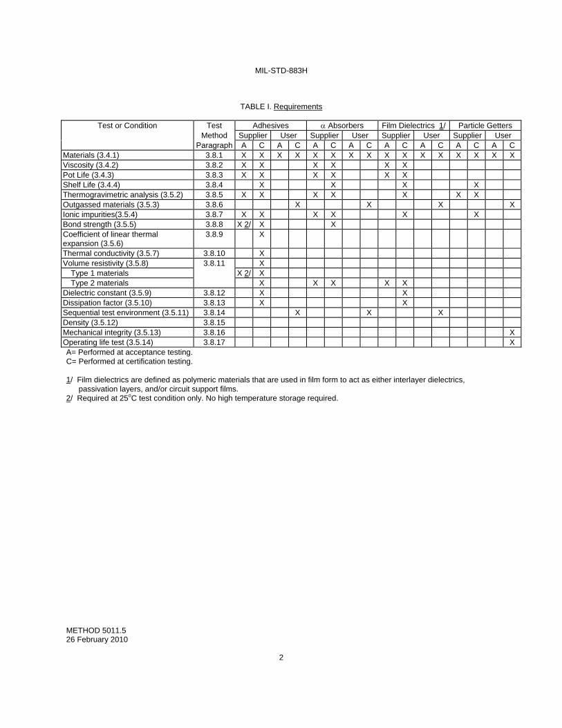
TABLE I. Requirements
Test or Condition Test Adhesives Absorbers Film Dielectrics 1/ Particle Getters
Method Supplier User Supplier User Supplier User Supplier User Paragraph A C A C A C A C A C A C A C A C
Materials (3.4.1) 3.8.1 X X X X X X X X X X X X X X X X Viscosity (3.4.2) 3.8.2 X X X X X X Pot Life (3.4.3) 3.8.3 X X X X X X Shelf Life (3.4.4) 3.8.4 X X X X Thermogravimetric analysis (3.5.2) 3.8.5 X X X X X X X Outgassed materials (3.5.3) 3.8.6 X X X X Ionic impurities(3.5.4) 3.8.7 X X X X X X Bond strength (3.5.5) 3.8.8 X 2/ X X Coefficient of linear thermal expansion (3.5.6)
3.8.9 X
Thermal conductivity (3.5.7) 3.8.10 X Volume resistivity (3.5.8) 3.8.11 X Type 1 materials X 2/ X Type 2 materials X X X X X Dielectric constant (3.5.9) 3.8.12 X X Dissipation factor (3.5.10) 3.8.13 X X Sequential test environment (3.5.11) 3.8.14 X X X Density (3.5.12) 3.8.15 Mechanical integrity (3.5.13) 3.8.16 X Operating life test (3.5.14) 3.8.17 X A= Performed at acceptance testing. C= Performed at certification testing. 1/ Film dielectrics are defined as polymeric materials that are used in film form to act as either interlayer dielectrics,
passivation layers, and/or circuit support films. 2/ Required at 25oC test condition only. No high temperature storage required.

MIL-STD-883H
METHOD 5011.5 26 February 2010
3
TABLE I. Requirements (Continued)
Test or Condition Test Method
Dessicants Junction Coatings T-Wave Absorbers Encapsulating Compounds
Paragraph Supplier User Supplier User Supplier User Supplier User A C A C A C A C A C A C A C A C Materials (3.4.1) 3.8.1 X X X X X X X X X X X X X X X X Viscosity (3.4.2) 3.8.2 X Pot Life (3.4.3) 3.8.3 Shelf Life (3.4.4) 3.8.4 X X X Thermogravimetric analysis (3.5.2) 3.8.5 X X X X X Outgassed materials (3.5.3) 3.8.6 X X X Ionic impurities(3.5.4) 3.8.7 X X X X X Bond strength (3.5.5) 3.8.8 X X Coefficient of linear thermal expansion (3.5.6)
3.8.9 X
Thermal conductivity (3.5.7) 3.8.10 X Volume resistivity (3.5.8) 3.8.11 X Type 1 materials Type 2 materials X X X Dielectric constant (3.5.9) 3.8.12 X Dissipation factor (3.5.10) 3.8.13 X Sequential test environment (3.5.11) 3.8.14 X X Density (3.5.12) 3.8.15 X X X X Mechanical integrity (3.5.13) 3.8.16 Operating life test (3.5.14) 3.8.17 X X A= Performed at acceptance testing. C= Performed at certification testing. 3.5 Properties of cured polymer materials. 3.5.1 Curing of polymer materials. The material must be capable of meeting the requirements of this document when cured according to the supplier's instructions. The cure schedule for supplier tests shall be identical for all tests and shall be reported. The cure schedule for the user tests shall be the minimum cure schedule plus, as a minimum, the pre-seal bake specified in the user's assembly document and shall be reported. Deviation from the suppliers recommended cure schedule will require verification by the user of the materials performance. 3.5.2 Thermogravimetric analysis (TGA). 3.5.2.1 Thermal stability. The thermal stability of the cured material shall be determined in accordance with 3.8.5. Unless otherwise noted, the weight loss at 200C shall be less than or equal to 1.0 percent of the cured material weight. Equivalent standard, i.e., "classical analytical techniques" are acceptable.
3.5.2.2 Filler content. Polymeric materials using a filler to promote properties such as electrical and thermal conductivity shall be tested in accordance with 3.8.5 to determine the inorganic filler content. For acceptance testing, the percent filler content shall not differ from the filler content in the certified materials by more than ±2 percent. 3.5.3 Outgassed materials. Outgassing of the cured material shall be determined in accordance with 3.8.6. Outgassed moisture, as determined in 3.8.6.1, shall be less than or equal to 5,000 ppmv (0.5 percent V/V) for 3 packages (0 failures) or 5 packages (1 failure). Other gaseous species present in quantities greater than or equal to 100 ppmv (0.01 percent V/V) shall be reported in ppmv or percent V/V. The data obtained in 3.8.6.2 shall also be reported in the same manner but for information only. The outgassing of the cured getter shall be determined in accordance with 3.8.6. The vapor content of the package with getter shall not exceed 2000 ppmv after 24 hours at 150C and 3000 ppmv after 1000 hours at 150C.

MIL-STD-883H
METHOD 5011.5 26 February 2010
4
3.5.4 Ionic impurities. The ionic impurity content shall be determined in accordance with 3.8.7 and shall meet the requirements specified in table II. Ionic content analysis shall be in triplicate for certification and single analysis for acceptance testing. Failure at acceptance shall require the passing of two additional samples.
TABLE II. Ionic impurity requirements.
Total ionic content specific electrical conductance) Hydrogen (pH) Chloride Sodium Potassium Flouride
< 4.50 millisiemens/meter 4.0 < pH < 9.0 < 200 ppm < 50 ppm < 50 ppm < 50 ppm
Other ions present in quantities > 5 ppm shall be reported in ppm. 3.5.5 Bond strength. The bond strength of a polymeric material shall be determined in accordance with 3.8.8 at 25C, and 25°C after 1,000 hours at 150°C. The bond strength shall meet as a minimum the 1.0X requirement specified in figure 2019-4 of method 2019 of MIL-STD-883 at each test condition. The manufacturer should test to shear or until twice the minimum 1.0X shear force is reached.

MIL-STD-883H
METHOD 5011.5 26 February 2010
5
3.5.6 Coefficient of linear thermal expansion. The coefficient of linear thermal expansion shall be determined from -65°C to 150°C in accordance with 3.8.9. The coefficient of linear thermal expansion shall be ±10% of the value required in the users material specification or purchase order. This requirement shall apply to the material as it is configured for actual use. This requirement shall not apply to glass supported polymeric films.
3.5.7 Thermal conductivity. The thermal conductivity shall be determined at 121°C ±5°C in accordance with 3.8.10. The thermal conductivity shall be greater than or equal to 1.5 watt/meter-K for type I polymers and greater than or equal to .15 watt/meter-K for type II polymers.
3.5.8 Volume resistivity. The volume resistivity shall be determined in accordance with 3.8.11. The volume resistivity of conductive materials at 25°C, at 60°C, at 150°C, and at 25°C after 1,000 hours at 150°C shall be less than or equal to 5.0 microhm-meter for silver-filled polymers and less than or equal to 15.0 microhm-meter for gold-filled polymers. The volume resistivity of insulative materials shall be greater than or equal to 0.1 teraohm-meter at 25°C and greater than or equal to 1.0 megohm-meter at 125°C. 3.5.9 Dielectric constant. The dielectric constant of insulative polymeric materials shall be determined in accordance with 3.8.12 and shall be less than or equal to 6.0 at both 1 kHz and 1 MHz for this type of polymer but shall be less than or equal to 3.5 at 1 kHz and 1 MHz for materials used for dielectric layers.
3.5.10 Dissipation factor. The dissipation factor of insulative polymers shall be determined in accordance with 3.8.13 and shall be less than or equal to 0.03 at 1 kHz and less than or equal to 0.05 at 1 MHz.
3.5.11 Sequential test environment. The polymeric material shall withstand exposure to the test conditions specified in 3.8.14. After exposure to the complete sequence of environmental conditions, the test specimens shall show no evidence of mechanical degradation. For adhesives the measured bond strength of components shall meet as a minimum the 1.0X requirement specified on figure 2019-4 of method 2019 of MIL-STD-883.
3.5.12 Density. The density of microwave or RF absorbing materials shall be tested in accordance with 3.8.15. The acceptable value shall be that which is within ±10% of the value required on the user's material specification or purchase order.
3.5.13 Mechanical integrity. Particle getter integrity shall be verified after different levels of environmental stress.
3.5.13.1 Getter integrity (short term). When tested in accordance with 3.8.16.1 all samples shall pass the criteria for PIND as defined in MIL-STD-883 method 2020.
3.5.13.2 Getter integrity (long term). When tested in accordance with 3.8.16.2 all samples shall pass the criteria for PIND as defined in MIL-STD-883, method 2020, both initially and after storage at 150°C for 1,000 hours. The salted particles shall remain attached to the getter material in the original position with no attachment and reattachment when viewed at 30X to 60X magnification.
3.5.13.3 Getter integrity (vibration). When tested in accordance with 3.8.16.3 the sample shall pass PIND as defined in MIL-STD-883, method 2020, the salted particles shall remain attached to the getter material in the original position, with no detachment and re-attachment when viewed at 30X to 60X.
3.5.14 Operating life. When tested in accordance with 3.8.17, the comparison between initial and post test electrical data shall not indicate parametric shifts, which are unique to the test group containing getter material.

MIL-STD-883H
METHOD 5011.5 26 February 2010
6
3.6 Responsibility for testing. The manufacturer and user are responsible for the performance of all tests as specified in
table I herein.
NOTE: The Government reserves the right to perform any of the inspections set forth in the specification where such inspections are deemed necessary to assure that supplies and services conform to prescribed requirements.
3.6.1 Test equipment and testing facilities. Test and measuring equipment and testing facilities of sufficient accuracy, quality and quantity to permit performance of the required testing shall be established and maintained by the manufacturer and user. The establishment and maintenance of a calibration system to control the accuracy of the measuring and test equipment shall be in accordance with ANSI/NCSL Z540.3 or equivalent. The supplier and user may utilize a commercial laboratory acceptable to the qualifying activity for performing the required certification and acceptance testing.
3.6.2 Testing conditions. Unless otherwise specified herein, all testing shall be performed in accordance with the test conditions specified in the "general requirements" of the MIL-STD-883.
3.7 Classification of testing. The test requirements specified herein are classified as certification testing and acceptance testing. 3.7.1 Certification testing. Certification testing shall be performed on the initial lot of material and for any major changes to the material thereafter and consist of all tests to determine conformance with all requirements specified herein. To insure that both the polymeric material and the processes employing the material are controlled, both the supplier and the user of the material shall be responsible for performance of the tests as designated in table I.
3.7.1.1 Sample size. The number of samples to be subjected to each testing procedure shall be as specified in the individual test methods.
3.7.1.2 Failures. Failure of any polymeric material to meet the testing requirements shall be cause for refusal to grant certification approval. 3.7.1.3 Retention of data. The data generated for certification shall be retained for a period of 5 years or until a recertification is performed, whichever is greater.
3.7.2 Acceptance testing. Acceptance tests shall be performed on each lot and shall consist of tests as specified in table I.
3.7.2.1 Test lot. A test lot shall consist of all polymeric material manufactured under the same batch number, i.e., a batch number identifies those materials whose constituents can be traced to a single lot of raw materials.
3.7.2.2 Sample size. The number of samples to be subjected to each testing procedure shall be as specified in the individual test methods.
3.7.2.3 Failures. Failure of the samples to meet the testing requirements of a specific test shall be cause for rejection of the lot.
3.7.2.4 Retention of data. The data generated for acceptance testing shall be retained for a period of 5 years. 3.8 Methods of examination and test. The following test criteria and analytical protocols shall be documented and approved by the qualifying activity prior to material certification.
3.8.1 Materials. The polymeric components or system or both shall be examined visually at a minimum magnification of 30X to ensure conformance with the requirements of 3.4.1.
*
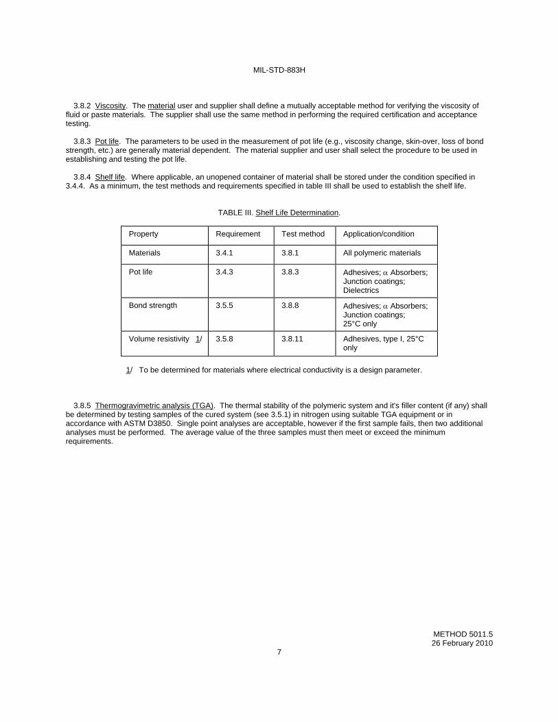
MIL-STD-883H
METHOD 5011.5 26 February 2010
7
3.8.2 Viscosity. The material user and supplier shall define a mutually acceptable method for verifying the viscosity of fluid or paste materials. The supplier shall use the same method in performing the required certification and acceptance testing.
3.8.3 Pot life. The parameters to be used in the measurement of pot life (e.g., viscosity change, skin-over, loss of bond strength, etc.) are generally material dependent. The material supplier and user shall select the procedure to be used in establishing and testing the pot life.
3.8.4 Shelf life. Where applicable, an unopened container of material shall be stored under the condition specified in 3.4.4. As a minimum, the test methods and requirements specified in table III shall be used to establish the shelf life.
TABLE III. Shelf Life Determination.
Property Requirement Test method Application/condition
Materials 3.4.1 3.8.1 All polymeric materials
Pot life 3.4.3 3.8.3 Adhesives; Absorbers; Junction coatings; Dielectrics
Bond strength 3.5.5 3.8.8 Adhesives; Absorbers; Junction coatings; 25°C only
Volume resistivity 1/ 3.5.8
3.8.11
Adhesives, type I, 25°C only
1/ To be determined for materials where electrical conductivity is a design parameter. 3.8.5 Thermogravimetric analysis (TGA). The thermal stability of the polymeric system and it's filler content (if any) shall be determined by testing samples of the cured system (see 3.5.1) in nitrogen using suitable TGA equipment or in accordance with ASTM D3850. Single point analyses are acceptable, however if the first sample fails, then two additional analyses must be performed. The average value of the three samples must then meet or exceed the minimum requirements.

MIL-STD-883H
METHOD 5011.5 26 February 2010
8
3.8.5.1 Thermal stability. The thermal stability of the polymeric material shall be determined by heating the specimens
from room temperature to not less than 210°C, at a heating rate between 10C/minute and 20°C/minute, in a nitrogen atmosphere with 20-30 milliliter/minute nitrogen flow. The weight loss at 200°C shall be determined. 3.8.5.2 Filler content. The filler content of polymeric materials using a filler to promote properties such as electrical or thermal conductivity shall be determined by heating the specimen from room temperature to 600°C, at a heating rate between 10°C/minute and 20°C/minute, in an air atmosphere with 20-30 milliliter/minute air flow. The temperature shall be maintained at 600°C until constant weight is obtained. It is permitted to perform 3.8.5.1, followed by heating from 210°C to 600°C as detailed above. The filler content shall be reported as weight percent of the cured specimen. 3.8.6 Outgassed materials. Ten test specimens shall be prepared using gold- or nickel-plated Kovar or ceramic packages, (dielectric materials may be prepared using aluminum coated silicon as the substrate). (The use of "leadless" packages is permitted to reduce moisture contributions due to package construction). The material shall be cured using the minimum cure schedule and shall receive the minimum pre-seal bake specified in the assembly document(s) (see 3.5.1). After a pre-seal bake, the packages shall be hermetically sealed. Only those packages that meet the fine and gross leak test requirements of test method 1014 shall be submitted for moisture content analysis. If less than 10 test specimens remain after hermetically testing, the failed packages shall be replaced by additional hermetical packages processed and tested in the same manner as the original group. 3.8.6.1 Testing for short term outgassing of moisture and other gaseous species. Five packages containing polymer prepared in accordance with 3.8.6 shall be heated in accordance with MIL-STD-883, method 1008, 24 hours at 150°C. The packages shall then be immediately (less than or equal to 5 minutes) inserted into the ambient gas analysis apparatus. The packages shall be subjected to ambient gas analysis in accordance with MIL-STD-883, method 1018, procedure 1. In addition to moisture, other gaseous species present in quantities greater than or equal to 100 ppmv (0.01 percent V/V) shall be reported in ppmv or percent V/V. This test shall meet the requirements of 3.5.3.
NOTE: From the 5 packages prepared in accordance with MIL-STD-883, method 1008, only 3 packages are required to be subjected to the ambient gas analysis testing and the pass criteria of 3 packages (0 failures) shall apply (see 3.5.3). However, in the event of a failure, the testing of the remaining 2 packages shall be required in order to pass with the criteria of 5 packages (1 failure).
All polymeric materials tested shall have quantities of material equivalent in mass and exposed surface area to that of the intended application. Gold plated Kovar tabs and alumina blanks may be used as facsimile device elements. Several polymeric materials of different application may be tested in combination with each other in this test, however their combined moisture content shall not exceed 5,000 ppmv.
3.8.6.2 Testing for long term outgassing of moisture and other gaseous species. Provided that the moisture requirement of 3.5.3 has been met by packages tested in 3.8.6.1, the remaining five devices containing polymer from the group prepared in accordance with 3.8.6 shall be heated in accordance with MIL-STD-883, method 1008 for 1,000 hours at 150°C. The packages shall then be immediately (less than or equal to 5 minutes) inserted into the ambient gas analysis apparatus. The packages shall be subjected to ambient gas analysis in accordance with MIL-STD-883, method 1018, procedure 1. In addition to moisture, other gaseous species present in quantities greater than or equal to 100 ppmv (0.01 percent V/V) shall be reported in ppmv or percent V/V.
3.8.7 Ionic impurities. A water-extract analysis shall be performed to determine the level of ionic contamination in the cured polymeric material. The total ion content (specific electrical conductance) and the specific ionic content for the hydrogen (pH), chloride, sodium, fluoride and potassium ions shall be measured. Other ions present in quantities > 5 ppm shall also be reported in ppm. The methods of analysis submitted in the following paragraphs are suggested techniques. Alternate methods of analysis may be selected where it can be shown that the techniques are equivalent and the method of analysis is approved by the qualifying activity. 3.8.7.1 Sample preparation. Adequate material shall be cured to obtain 3 gram samples of polymer following grinding, for final preparation. The material shall be cured on teflon or other inert surface in a forced draft oven. When possible the cured specimen shall be removed from the curing substrate and ground to 60-100 mesh particles; polymeric film samples less than or equal to 0.025 cm thick shall be cured and cut into less than or equal to 0.25 cm2 samples; gels or low modulus materials may be cast directly into the flat bottom of the sample flask for the extraction. Smaller sample sizes may be selected where it can be shown that the accuracy of the test method has not changed.

MIL-STD-883H
METHOD 5011.5 26 February 2010
9
3.8.7.2 Extraction procedure. 3 grams (equivalent resin) of the ground or cut equivalent polymer shall be added to a cleaned; tarred, 250-ml flasks made of pyrex, or equivalent. The weight of the cured material in each flask shall be recorded to the nearest milligram. 150.0 grams of deionized water with a measured specific conductance less than or equal to 0.1 millisiemens/meter (specific resistivity greater than or equal to 1.0 megohm-centimeter) shall be added to the flask. A blank shall be prepared by adding 150.0 grams of the deionized water and a boiling chip to a second 250-ml flask. The flasks shall be refluxed for 20 hours.
NOTE: 1.0 mho = 1.0 siemens; 1.0 mho/cm = 100.0 siemens/meter.
3.8.7.3 Measurement of ionic content. 3.8.7.3.1 Total ionic content. The total extractable ionic content shall be determined by measuring the specific electrical conductance of the water-extract samples and the blank using a conductivity meter with an immersion conductivity cell having a cell constant of 0.01/centimeter (alternatively 0.1 cm-1 to adjust for proper analysis of the solution). The total ionic content, in millisiemens/meter, shall be obtained by subtracting the specific conductance of the blank from the specific conductance of the samples.
3.8.7.3.2 Hydrogen ion content (pH). The pH of the water extract shall be determined using a pH meter with a standard combination electrode. 3.8.7.3.3 Specific ion analysis. Specific ion analysis of the water extract shall be conducted using ion chromatography or a demonstrated equivalent. The ion concentrations in the extract shall be converted to the sample extractable concentrations by multiplying the ratio of the deionized water weight (W) to polymer sample weight (S); that is, by (W/S). The chloride, sodium, fluoride and potassium ion levels and all other ions detected in quantities > 5 ppm shall be reported in ppm. 3.8.8 Bond strength. The bond strength of the polymeric material shall be determined in accordance with 3.8.8.1, 3.8.8.2 or 3.8.8.3 below. As a minimum, five elements shall be tested to failure at the following conditions:
a. At 25°C. b. At 25°C after 1,000 hours at 150°C in an air or nitrogen ambient.
The average bond strength at each test condition shall be determined in kilograms (force). 3.8.8.1 Bond strength. The bond strength shall be determined in accordance with method 2019 of MIL-STD-883. A gold-metallized substrate or a gold- or nickel-plated package shall be used as the bonding surface for bond strength testing. 3.8.8.1.1 Type I materials. Suppliers shall use 0.08 inch-square (0.2 centimeter-square) gold-plated Kovar tabs. 3.8.8.1.2 Type II materials. Suppliers shall use 0.08 inch-square (0.2 centimeter-square) alumina chips. 3.8.8.2 Bond strength. The bond strength may be determined in accordance with ASTM D1002 as an alternative to test method 2019. If ASTM D1002 is used, the results must be correlated to assure that the bond strength of the adhesive is shown to be equivalent to the Method 2019 failure criteria. 3.8.8.3 Molding compounds or encapsulants. Molding compounds or encapsulants shall be tested in accordance with MIL-STD-883, test method 1034.

MIL-STD-883H
METHOD 5011.5 26 February 2010
10
3.8.9 Coefficient of linear thermal expansion. The coefficient of linear thermal expansion shall be determined in accordance with ASTM E831 over the temperature range of -65°C to 150°C. The glass transition temperature, coefficients, and temperature ranges corresponding to different slopes of the curve shall be noted.
3.8.10 Thermal conductivity. The thermal conductivity, in watt/meter-K, shall be determined at 121°C ±5°C in accordance with ASTM C177 or ASTM C518.
NOTE: 1 cal/cm-s-k = 418.4 W/m-K.
3.8.11 Volume resistivity.
3.8.11.1 Type I polymers.
3.8.11.1.1 Paste materials. Test specimens shall be prepared using a standard 1 inch x 3 inch glass slide. A jig capable of holding this slide, with two scribed lines 100 mil apart and parallel to the length, shall be the guide for applying two strips of transparent tape. There shall be no wrinkles or bubbles in the tape. The slide shall be cleaned with alcohol and air dried. A drop of the type I material shall be placed between the two strips of tape. Using a single edge razor blade maintaining a 30 angle between the slide surface and the razor blade, the material shall be squeezed between the tape strips. The length of the applied strip shall be at least 2.5 inches. The tape shall be removed, and the material shall be cured according to 3.5.1. After cure, the test specimens shall be allowed to cool to room temperature.
3.8.11.1.2 Film materials. Test specimens shall be prepared using a standard 1 inch x 3 inch glass slide. The slide shall be cleaned with alcohol and air dried. A thin strip of the uncured film approximately 100 mil wide and at least 2.5 inches long shall be placed on the glass slide. The film shall be covered with a strip of copper foil or Teflon film and a second 1 inch x 3 inch glass slide shall be placed over the foil or Teflon film. Sufficient force (weight, clip, etc.), shall be applied to the assembly to compress the material during cure. The material shall be cured according to 3.5.1. After cure, the test specimen shall be allowed to cool to room temperature, and the top slide and foil or Teflon shall be removed. The exact width and thickness of each polymer strip shall be measured with a precision caliper and micrometer respectively. These measurements, after conversion to the appropriate units, shall be used to calculate the volume resistivity using the formula given in 3.8.11.1.3.
3.8.11.1.3 Resistance measurements. Resistance measurements shall be made using a milliohm meter in conjunction with a special four-point probe test fixture. (This fixture can be made of an acrylic material with four spring-loaded contacts. The contacts must be set into the acrylic so that the current contacts are 2 inches apart, the voltage contacts are between the two current contacts, and the voltage contacts are separated from each current contact by 0.5 inch.) The four-point probe fixture shall be placed on the strip of conductive polymer and contact between each probe and the material shall be ensured. The measured resistance shall be recorded in ohms, and the resistivity shall be determined from the following formula:
P = R (w x t)
l
Where:
P = resistivity, ohm-m
R = measured resistance, ohms
w = width, (100 mil = 2.54 mm)
t = thickness, (micrometer reading of the material plus glass side) minus (micrometer reading of the glass slide)
l = length between inner pair of probes, (1 inch = 25.4 mm)
A minimum of three specimens shall be tested at 25°C, at 60°C, at 150°C, and at 25°C after 1,000 hours at 150°C in an air or nitrogen ambient. The same specimens may be used for each test.
*
MIL-STD-883H
METHOD 5011.5 26 February 2010
11
3.8.11.2 Type II polymer materials. Type II materials shall be tested in accordance with ASTM D257 at temperatures of 25°C and 125°C.
3.8.12 Dielectric constant. The dielectric constant of type II materials shall be determined as required in the user's material specification in accordance with ASTM D150 at frequencies of 1 kHz and 1 MHz at room temperature.
3.8.13 Dissipation factor. The dissipation factor of type II materials shall be determined as required in the user's material specification in accordance with ASTM D150 at frequencies of 1 kHz and 1 MHz at room temperature.
3.8.14 Sequential test environment. Testing shall be performed using either 3.8.14.1 or 3.8.14.2. 3.8.14.1 Sequential test environment. A minimum of five test specimens shall be subjected to the environmental conditions specified below. Specimens shall be prepared using the largest component/substrate/package combinations representative of end-use applications in backing material, attach surface, and size. Component types include resistor, capacitor, integrated circuit, and discrete semiconductor elements. Two components of each type shall be attached to the substrate with the adhesive (type I or II) proposed for use with that component type. The test specimens shall be subjected to the following environmental conditions in the sequence given:
a. Thermal shock (MIL-STD-883, method 1011, condition C, 15 cycles).
b. Temperature cycling (MIL-STD-883, method 1010, condition C, 100 cycles).
c. Mechanical shock (MIL-STD-883, method 2002, condition B, Y1 only).
d. Variable frequency vibration (MIL-STD-883, method 2007, condition A, Y1 only).
e. Constant acceleration (MIL-STD-883, method 2001, condition B, Y1 only). 3.8.14.2 Alternate sequential testing. Alternatively, testing in accordance with Qualification Testing (QML sequences in accordance with MIL-PRF-38534, using maximum baseline limits may be performed. The user is still required to satisfy the requirements of 3.8.14.1 by completing the necessary supplemental testing, i.e., thermal shock and vibration.
Following the environmental exposures of 3.8.14.1 or 3.8.14.2, the test specimens shall be examined for possible degradation in accordance with MIL-STD-883, method 2017. For adhesives, one of each type of component from each sample shall be evaluated for die shear strength in accordance with MIL-STD-883, method 2019 and shall meet the strength requirements of figure 2019-4.
3.8.15 Density. The density of materials used as RF or microwave absorbers shall be determine in accordance with
principles outlined in ASTM D1564, paragraphs 69-74. Those RF absorbers that are foamed in-place are to be foamed, cured, and cut to form the free standing material for this analysis.

MIL-STD-883H
METHOD 5011.5 26 February 2010
12
3.8.16 Mechanical integrity.
3.8.16.1 Getter integrity - short term. Samples shall be prepared using hermetically sealed packages representative of the maximum size and type which will incorporate the use of getter material. These samples will contain only "salted" particles and getter material. The getter material shall be applied to the package in the location and approximate volume as specified for a normal production part. The getter material coverage area shall be measured and recorded. The particles to be salted shall consist of the following unless otherwise agreed upon by the user and the qualifying activity.
(1) Solder balls: 3-6 mils in diameter - 2 pieces required.
(2) Aluminum ribbon: Approximate dimensions of 2 mil thick by 5 mil wide by 10 mils long - 1 required. A piece of aluminum wire 2-6 mils in diameter may be substituted for the ribbon.
(3) Gold wire: 1 mil diameter by 15-20 mils in length - 1 piece required. Getter material
application and cure shall take place in the sequence normally followed for production parts. The samples shall be processed through the same environmental conditioning steps as a qualified production part. The samples shall be subjected to PIND test in accordance with MIL-STD-883, method 2020, condition A or B, which shall be repeated three time for a total of four cycles to verify the integrity of the getter material. During all PIND testing the samples shall be mounted on the tester such that the shock pulses integral with the test shall be in the direction most likely to dislodge the particles from the getter material. A minimum of three samples shall be evaluated and all shall pass the defined PIND criteria.
3.8.16.2 Getter integrity - long term. All of the conditions and requirements of 3.8.16.1 apply, except that the samples either newly prepared or as received from the short term test, shall be stored at 150°C for 1,000 hours.
The samples shall then be subjected to mechanical shock in accordance with MIL-STD-883, method 2002, condition B, in the Y2 direction. Following mechanical shock the samples shall be PIND tested as specified above.
Following PIND, the samples shall be delidded and a visual inspection shall be performed to verify the following:
a. Determine if particles have separated from the getter material or have fallen into the package. b. Determine if getter coverage has spread or bled out. c. Check for any evidence of peeling from inside and/or getter becoming separated from package.
3.8.16.3 Vibration. Samples shall be prepared as in 3.8.16.1 except that the lid shall be attached in such a manner that it may be removed for visual inspection. After particle salting and immobilization as in 3.8.16.1, visual inspection shall be done to verify entrapment of the salted particles. Location of the particles in the getter material shall be recorded for future reference. The lid shall then be reattached to the package securely enough to withstand the testing that follows. After PIND testing in accordance with MIL-STD-883, method 2020, the samples shall be subjected to vibration in accordance with MIL-STD-883, method 2007, condition A or B. At the end of this test, the lids shall be removed from the package by whatever method is required. Location of the "salted" particles in the getter material shall be noted and compared with the location prior to vibration. Particles other than the original "salted" particles shall be ignored. A minimum of three samples shall be submitted for evaluation and all shall pass the defined PIND criteria initially and after vibration.

MIL-STD-883H
METHOD 5011.5 26 February 2010
13
3.8.17 Operating life test. Ten electrically functioning samples shall be fabricated using hermetically sealed devices which have been processed through the same steps as a normally qualified production part as specified by the user's assembly drawing. If agreed upon by the user and the qualifying activity, standard evaluation circuits may be substituted. All the samples shall meet the PIND test requirements in accordance with MIL-STD-883, method 2020, condition A or B. The samples shall be subjected to the life test in accordance with MIL-STD-883, method 1005, condition A, for 1,000 hours at 125°C. Electrical parameters shall be measured and recorded for the units initially and at the completion of the life test. Data taken from the samples shall be reviewed for evidence of device degradation due to the presence of getter material. NOTE: Qualification test data may be used to satisfy this requirement with qualifying activity approval.
3.9 Test deviation. Additional, reduced or alternate testing, as may be dictated by the uniqueness of particular material and manufacturing construction techniques can be required or authorized by the qualifying activity provided the manufacturer submits data to support test deviation.
4. SUMMARY. As a minimum, acquisition documents shall specify the following information:
a. Title, number, and revision letter of acquisition specification. b. Size and number of containers required. c. Manufacturer's product designation. d. Request for test data.

MIL-STD-883H
METHOD 5011.5 26 February 2010
14
This page intentionally left blank

MIL-STD-883H
METHOD 5012.1 27 July 1990
1
METHOD 5012.1
FAULT COVERAGE MEASUREMENT FOR DIGITAL MICROCIRCUITS 1. PURPOSE. This test procedure specifies the methods by which fault coverage is reported for a test program applied to a microcircuit herein referred to as the device under test (DUT). This procedure describes requirements governing the development of the logic model of the DUT, the assumed fault model and fault universe, fault classing, fault simulation, and fault coverage reporting. This procedure provides a consistent means of reporting fault coverage regardless of the specific logic and fault simulator used. Three procedures for fault simulation are described in this procedure: Full fault simulation and two fault sampling procedures. The applicable acquisition document shall specify a minimum required level of fault coverage and, optionally, specify the procedure to be used to determine the fault coverage. A fault simulation report shall be provided that states the fault coverage obtained, as well as documenting assumptions, approximations, and procedures used. Where any technique detailed in this procedure is inapplicable to some aspect of the logic model, or inconsistent with the functionality of the available fault simulator and simulation postprocessing tools, it is sufficient that the user of this procedure employ an equivalent or comparable technique and note the discrepancy in the fault simulation report. Microcircuits may be tested by nontraditional methods of control or observation, such as power supply current monitoring or the addition of test points that are available by means of special test modes. Fault coverage based on such techniques shall be considered valid if substantiating analysis or references are provided in the fault simulation report. 1.1 Terms. Terms and abbreviations not defined elsewhere in the text of this test procedure are defined in this section. a. Automatic test equipment (ATE). The apparatus with which the actual DUT will be tested. ATE includes the
ability to apply a test vector sequence (see 1.1l). b. Broadside application. A method of applying a test vector sequence where input stimuli change only at the
beginning of a simulation cycle or ATE cycle and all changes on primary inputs of the DUT are assumed to be simultaneous. Nonbroadside application occurs when test vectors are conditioned by additional timing information such as delay (with respect to other primary inputs), return-to-zero, return-to-one, and surround-by- complement.
c. Detection. An error at an observable primary output of a logic model caused by the existence of a logic fault. A
hard detection is where an observable output value in the fault-free logic model is distinctly different from the corresponding output value in the faulty logic model. An example of a hard detection is where the fault-free logic model's output value is 0 and the faulty logic model's output value is 1, or where the fault-free logic model's output value is 1 and the faulty logic model's output value is 0. If the high-impedance state (Z) can be sensed by the ATE, then a hard detection can involve the Z state as well. A potential detection is an error where the fault-free output is 0 or 1 and the faulty output value is unknown (X), or Z if Z cannot be sensed by the ATE.
d. Established test algorithm. An algorithm, procedure, or test vector sequence, that when applied to a logic
component or logic partition has a known fault coverage or test effectiveness. This fault coverage or test effectiveness is denoted herein as the established fault coverage or established test effectiveness for the established test algorithm. For example, an established test algorithm for a RAM may be a published memory test algorithm, such as GALPAT, that has been shown by experience to detect essentially all RAM failures and therefore is assessed an established test effectiveness of 100 percent. An ALU may be tested by means of a precomputed test vector sequence for which fault coverage has been previously determined. More than one established test algorithm may exist for a logic component or logic partition, each with a different established fault coverage or test effectiveness.

MIL-STD-883H
METHOD 5012.1 27 July 1990
2
e. Failure hierarchy: Failure mechanism, physical failure, logical fault, error. The failure hierarchy relates physical
defects and their causes to fault simulators and observable effects. A failure mechanism is the actual cause of physical failure; an example is electromigration of aluminum in a microcircuit. A physical failure (or simply failure) is the actual physical defect caused by a failure mechanism; an example is an open metal line. A logical fault (or simply fault) is a logical abstraction of the immediate effect of a failure; an example is "stuck- at-one" behavior of a logic gate input in the presence of an open metal line. An error is a difference between the behavior of a fault-free and faulty DUT at one or more observable primary outputs of the DUT.
f. Fault coverage. For a logic model of a DUT, a fault universe for the logic model of the DUT, and a given test
vector sequence, fault coverage is the fraction obtained by dividing the number of faults contained in the fault universe that are detected by the test vector sequence by the total number of faults contained in the fault universe. Fault coverage is also stated as a percentage. In this test procedure, fault coverage is understood to be based on the detectable fault equivalence classes (see 3.3). Rounding of fault coverage fractions or percentages shall be "toward zero," not "to nearest." For example, if 9,499 faults are detected out of 10,000 faults simulated, the fault coverage is 94.99 percent; if this value is to be rounded to two significant digits, the result shall be reported as 94 percent, not 95 percent.
g. Logic line, node. Logic lines are the connections between components in a logic model, through which logic
signals flow. Logic lines are the idealized "wires" in a logic model. A set of connected logic lines is a node. h. Logic: Combinational and sequential. Combinational digital logic contains only components that do not possess
memory, and in which there are no feedback paths. Sequential digital logic contains at least one component that contains memory, or at least one feedback path, or both. For example, a flip-flop is a component that contains memory, and cross-coupled logic gates introduce feedback paths.
i. Macro. A logic modeling convention representing a model contained within another model. A macro boundary
does not necessarily imply the existence of a physical boundary in the logic model. A main model is a logic model that is not contained within a larger model. Macros may be nested (that is, a macro may contain submacros).
j. Primary inputs, primary outputs. Primary inputs to a logic model represent the logic lines of a DUT that are driven
by the ATE's drivers and thus are directly controllable test points. Primary outputs from a logic model represent the logic lines of the DUT that are sensed by the ATE's comparators and thus are directly observable test points. The inputs to the "main model" of the logic model of the DUT are the primary inputs, and the outputs from the main model are the primary outputs. Internal nodes that can be driven or sensed by means of special test modes shall be considered to be control or observation test points.
k. Test effectiveness. A measure similar to fault coverage, but used in lieu of fault coverage in cases where physical
failures cannot be modeled accurately as logical faults. For example, many RAM and PLA failures cannot be idealized conveniently in the same way as gate-level failures. However, established test algorithms may be used to detect essentially all likely physical failures in such structures.
l. Test vector sequence. The (ordered) sequence of stimuli (applied to a logic model of a DUT) or
stimulus/response values (applied to, and compared for, the actual DUT by the ATE). m. Undetectable and detectable faults. An undetectable fault is defined herein as a logical fault for which no test
vector sequence exists that can cause at least one hard detection or potential detection (see 1.1c). Otherwise (that is, some test vector sequence exists that causes at least one hard detection, or potential detection, or both), the fault is defined herein to be a detectable fault (see 3.3.3).

MIL-STD-883H
METHOD 5012.1 27 July 1990
3
2. APPARATUS. 2.1 Logic simulator. Implementation of this test procedure requires the use of a facility capable of simulating the behavior of fault-free digital logic in response to a test vector sequence; this capability is herein referred to as logic simulation. In order to simulate sequential digital logic, the simulator must support simulation of a minimum of four logic states: zero (0), one (1), high-impedance (Z), and unknown (X). In order to simulate combinational digital logic only, the simulator must support simulation of a minimum of two logic states: 0 and 1. At the start of logic simulation of a logic model of a DUT containing sequential logic, the state of every logic line and component containing memory shall be X; any other initial condition, including explicit initialization of any line or memory element to 0 or 1, shall be documented and justified in the fault simulation report. In order to simulate wired connections or bus structures, the simulator must be capable of resolving signal conflicts introduced by such structures. Otherwise, modeling workarounds shall be permitted to eliminate such structures from the logic model (see 3.1.2). In order to simulate sequential digital logic, the simulator must support event- directed simulation. As a minimum, unit-delay logic components must be supported. Simulation of combinational-only logic, or simulation of sequential logic in special cases (such as combinational logic extracted from a scannable sequential logic model) can be based on nonevent-directed simulation, such as levelized, zero-delay, or compiled-code methods. The fault simulation report shall describe why the selected method is equivalent to the more general event-directed method. 2.2 Fault simulator. In addition to the capability to simulate the fault-free digital logic, the capability is also required to simulate the effect of single, permanent, stuck-at-zero and stuck-at-one faults on the behavior of the logic; this capability is herein referred to as fault simulation. Fault simulation shall reflect the limitations of the target ATE (see 3.4.1). It is not necessary that the fault simulator directly support the requirements of this test procedure in the areas of hard versus potential detections, fault universe selection, and fault classing. However, the capability must exist, at least indirectly, to report fault coverage in accordance with this procedure. Where approximations arise (for example, where fault classing compensates for a different method of fault universe selection) such differences shall be documented in the fault simulation report, and it shall be shown that the approximations do not increase the fault coverage obtained. 3. PROCEDURE. 3.1 Logic model. 3.1.1 Level of modeling. The DUT shall be described in terms of a logic model composed of components and connections between components. Primary inputs to the logic model are assumed to be outputs of an imaginary component (representing the ATE's drivers), and primary outputs of the logic model are assumed to be inputs to an imaginary component (representing the ATE's comparators). Some logic simulators require that the ATE drivers and comparators be modeled explicitly; however, these components shall not be considered to be part of the logic model of the DUT. 3.1.2 Logic lines and nodes (see 1.1g). All fan-out from a node in a logic model is ideal, that is, fan-out branches associated with a node emanate from a single point driven by a fan-out origin. All fan-in to a node in a logic model is ideal; that is, multiple fan-in branches in a node drive a single line. Figure 1 shows a node that includes fan-in branches, a fan-out origin, and fan-out branches. Because fan-in and fan-out generally are not ideal in actual circuit layout, the actual topology of the circuit should be modeled, if it is known, by appropriately adding single-input noninverting buffers to the logic model. Modeling workarounds may be used to eliminate fan-in to a node. This may be required if the simulator does not directly model wired connections or bus structures. Some simulators may permit internal fan-in, but require that bidirectional pins to a DUT be modeled as separate input and output functions.

MIL-STD-883H
METHOD 5012.1 27 July 1990
4
3.1.3 G-logic and B-logic partitions. Simple components of the logic model (logic primitives such as AND, OR, NAND, NOR, XOR, buffers, or flip-flops; generally the indivisible primitives understood by a simulator) are herein referred to as gate logic (G-logic). Complex components of the logic model (such as RAM, ROM, or PLA primitive components, and behavioral models - relatively complex functions that are treated as "black boxes" for the purpose of fault simulation) are referred to herein as block logic (B-logic). For the purpose of fault simulation, the logic model shall be divided into nonoverlapping logic partitions; however, the entire logic model may consist of a single logic partition. The logic partitions contain components and their associated lines; although lines may span partitions, no component is contained in more than one partition. A G-logic partition contains only G-logic; any other logic partition is a B-logic partition. A logic partition consisting of G-logic, or B-logic, or G-logic and B-logic that, as a unit, is testable using an established testing algorithm, with known fault coverage or test effectiveness, may be treated as a single B-logic partition. 3.1.4 Model hierarchy. The logic model may be hierarchical (that is, consisting of macro building blocks), or flat (that is, a single level of hierarchy with no macro building blocks). Hierarchy does not impose structures on lines; for example, there is no implied fan-out origin at a macro input or output. Macros that correspond to physical partitions in a model shall use additional buffers (or an equivalent method) to enforce adherence to the actual DUT's fan-out. 3.1.5 Fractions of transistors. The fraction of transistors comprising each G-logic and B-logic partition, with respect to the total count of transistors in the DUT, shall be determined or closely estimated; the total sum of the transistor fractions shall equal 1. Where the actual transistor counts are not available, estimates may be made on the basis of gate counts or microcircuit area; the assumptions and calculations supporting such estimates shall be documented in the fault simulation report. The transistor fractions shall be used in order to weight the fault coverage measured for each individual logic partition (see 3.5). 3.2 Fault model. 3.2.1 G-logic. The fault model for G-logic shall be permanent stuck-at-zero and stuck-at-one faults on logic lines. Only single stuck-at faults are considered in calculating fault coverage. 3.2.2 B-logic. No explicit fault model is assumed for B-logic components. However, an established test algorithm shall be applied to each B-logic component or logic partition. If a B-logic partition contains logic lines or G-logic components, or both, justification shall be provided in the fault simulation report as to how the established test algorithm that is applied to the B-logic partition detects faults associated with the logic lines and G-logic components. 3.2.2.1 Built-in self-test. A special case of B-logic is a partition that includes a linear-feedback shift register (LFSR) that performs signature analysis for compression of output error data. Table I lists penalty values for different LFSR degrees. If the LFSR implements a primitive GF(2) polynomial of degree "k", where there is at least one flip-flop stage between inputs to a multiple-input LFSR, then the following procedure shall be used in order to determine a lower bound on the established fault coverage of the logic partition: Step 1: Excluding the LFSR, but including any stimulus generation logic considered to be part of the logic partition,
determine the fault coverage of the logic partition by fault simulation without signature analysis; denote this fault coverage by C.
Step 2: Reference table I. For a given degree "k" obtain the penalty value "p". The established fault coverage of the
logic partition using a LFSR of degree "k" shall be reported as (1-p)C. That is, a penalty of (100p) percent is incurred in assessing the effectiveness of signature analysis if the actual effectiveness is not determined.

MIL-STD-883H
METHOD 5012.1 27 July 1990
5
3.3 Fault universe selection and fault equivalence classing. Fault coverage shall be reported in terms of equivalence classes of the detectable faults. This section describes the selection of the initial fault universe, the partitioning or collapsing of the initial fault universe into fault equivalence classes, and the removal of undetectable faults in order to form the detectable fault universe. These three stages constitute the fault simulation reporting requirements; however, it is generally more efficient to obtain the set of faults that represent the fault equivalence classes directly without explicitly generating the initial fault universe. 3.3.1 Initial fault universe. The initial fault universe shall consist of single, permanent, stuck-at-zero and stuck-at-one faults on every logic line (not simply on every logic node) in the G-logic partitions of the logic model. A bus, which is a node with multiple driving lines, shall be considered, for the purpose of fault universe generation, to be a multiple-input, single-output logic gate. The initial fault universe shall include stuck-at-zero and stuck-at-one faults on each fan-in and fan-out branch and the fan-out origin of the bus (see figure 1). The fault universe does not explicitly contain any faults within B-logic partitions. However, all faults associated with inputs and outputs of B-logic components either are contained in a G-logic partition or shall be shown to be considered by established test algorithms that are applied to the B-logic partitions. No faults shall be added or removed by considering or not considering logic model hierarchy. No extra faults shall be associated with any primary input or output line, macro input or output line, or logic line that spans logic partitions where the logic partitions do not correspond to a physical boundary. No more than one stuck-at-zero and one stuck-at-one fault per logic line shall be contained in the initial fault universe. 3.3.2 Fault equivalence classes. The initial fault universe shall be partitioned or collapsed into fault equivalence classes for reporting purposes. The fault equivalence classes shall be chosen such that all faults in a fault equivalence class cause apparently identical erroneous behavior with respect to the observable outputs of the logic model. One fault from each fault equivalence class shall be selected to represent the fault class for reporting purposes; these faults shall be called the representative faults. For the purpose of implementing this test procedure it is sufficient to apply simple rules to identify structurally-dependent equivalence classes. An acceptable method for selecting the representative faults for the initial fault universe consists of listing all single, permanent, stuck-at faults as specified in table II. Any other fault equivalencing procedure used shall be documented in the fault simulation report. If a bus node exhibits wired-AND or wired-OR behavior in the applicable circuit technology, then faults associated with that bus shall be collapsed in accordance with the AND or OR fault equivalencing rules, respectively. Otherwise, no collapsing of faults associated with a bus shall be performed. 3.3.3 Detectable fault universe. Fault coverage shall be based on the detectable fault universe. Undetectable faults shall be permitted to be dropped from the set of representative faults; the remaining set of representative faults comprises the detectable fault universe. In order for a fault to be declared as undetectable, documentation shall be provided in the fault simulation report as to why there does not exist any test vector sequence capable of guaranteeing that the fault will cause an error at an observable primary output (see 1.1m.). Any fault not documented in the fault simulation report as being undetectable shall be considered detectable for the purpose of calculating fault coverage.

MIL-STD-883H
METHOD 5012.1 27 July 1990
6
3.4 Fault simulation. 3.4.1 Automatic test equipment limitations. Fault coverage reported for the logic model of a DUT shall reflect the limitations of the target ATE. Two common cases are: a. Fault detection during fault simulation shall occur only at times where the ATE will be capable of sensing the
primary outputs of the DUT; there must be a one-to-one correspondence between simulator compares and ATE compares. For example, if fault coverage for a test vector sequence is obtained using broadside fault simulation (where fault detection occurs after every change of input stimuli, including clock signals), then it is not correct to claim the same fault coverage on the ATE if the test vectors are reformatted into cycles where a clock signal is pulsed during each cycle and compares occur only at the end of each cycle.
b. If the ATE cannot sense the Z output state (either directly or by multiple passes), then the reported fault coverage
shall not include detections involving the Z state. That is, an output value of Z shall be considered to be equivalent to an output value of X.
Any differences in format or timing of the test vector sequence, between that used by the fault simulator and that
applied by the ATE, shall be documented in the fault simulation report and it shall be shown that fault coverage achieved on the ATE is not lower than the reported fault coverage.
3.4.2 G-logic. 3.4.2.1 Hard detections and potential detections. Fault coverage for G-logic shall include only faults detected by hard detections. Potential detections shall not be considered directly in calculating the fault coverage. No number of potential detections of a fault shall imply that the fault would be detected. Some potential detections can be converted into hard detections for the purpose of calculating fault coverage. If it can be shown that a fault is only potentially detected by fault simulation but is in fact detectable by the ATE by a difference not involving an X value, then upon documenting those conditions in the fault simulation report that fault shall be considered to be detected as a hard detection and the fault coverage shall be adjusted accordingly. Faults associated with three-state buffer enable signal lines can cause X states to occur on nodes with fan-in branches, or erroneous Z states to occur on three-state primary outputs that may be untestable on some ATE. These faults may then be detectable only as potential detections, but may be unconvertible into hard detections. In such cases, it is permissible for the fault simulation report to state separately the fraction of the undetected faults that are due to such faults. 3.4.2.2 Fault simulation procedures. The preferred method of fault simulation for G-logic is to simulate the effect of each representative fault in the G-logic. However, this may not be practical in some cases due to the large number of representative faults, or because of limitations of the logic models or simulation tools. In such cases fault sampling procedures may be used. When fault sampling is used, either the acquisition document shall specify the method of obtaining a random sample of faults or the fault simulation report shall describe the method used. In either case, the complete random sample of faults shall be obtained before beginning the fault simulation procedure involving a random sample of faults. Use of any fault simulation procedure other than fault simulation procedure 1 (see 3.4.2.2.1) shall be documented and justified in the fault simulation report. In this section, it is assumed that the representative faults declared to be undetectable have been removed from the set of faults to be simulated.

MIL-STD-883H
METHOD 5012.1 27 July 1990
7
3.4.2.2.1 Fault simulation procedure 1. Simulate each representative fault in a G-logic partition. The procedure used shall be equivalent to the following: Step 1: Denote by "n" the total number of representative faults in the G-logic partition. Step 2: Fault simulate each representative fault. Denote by "d" the number of hard detections. Step 3: Fault coverage for the G-logic partition is given by d/n. 3.4.2.2.2 Fault simulation procedure 2. Obtain lower bound on actual fault coverage in a G-logic partition using fixed sample size (see table III). The procedure used shall be equivalent to the following: Step 1: Select a value for the penalty parameter "r" (r = 0.01 to 0.05). The corresponding value of "n" in table III is the
size of the random sample of representative faults. Step 2: Fault simulate each of the "n" representative faults. Denote by "d" the number of hard detections. Step 3: The lower bound on the fault coverage is given by "d/n-r". 3.4.2.2.3 Fault simulation procedure 3. Accept/reject lower bound on fault coverage in a G-logic partition using fixed sample size (see table IV). The procedure used shall be equivalent to the following: Step 1: Denote by "F" the minimum required value for fault coverage. From table IV obtain the minimum required
sample size, denoted by "n". Step 2: Fault-simulate each of the "n" representative faults, and denote by "d" the number of hard detections. Step 3: If "d" is less than "n" (that is, any faults are undetected), then conclude that the fault coverage is less than "F."
Otherwise (that is, all sampled faults are detected), conclude that the fault coverage is greater than or equal to "F". 3.4.3 B-logic. Fault coverage shall be measured indirectly for each B-logic partition. For a given B-logic partition, the established fault coverage or test effectiveness shall be reported for that B-logic partition only if it is shown that: (a) the test vector sequence applied to the DUT applies the established test algorithm to the B-logic partition, and (b) the resulting critical output values from the B-logic partition are made observable at the primary outputs. Otherwise, the fault coverage for that B-logic partition shall be reported as 0 percent. For each B-logic partition tested in this way, the established test algorithm, proof of its successful application, and the established fault coverage or test effectiveness shall be documented in the fault simulation report. 3.5 Fault coverage calculation. Let "m" denote the number of logic partitions in the logic model for the DUT. For the ith logic partition, let "Fi" denote its fault coverage (measured in accordance with 3.4), and let "Ti" denote its transistor fraction (measured in accordance with 3.1.5). The fault coverage "F" for the logic model for the DUT shall be calculated as:
F = F T + F T + ... + F T1 2 2 2 m m If fault simulation procedure 1 is performed for each G-logic partition in the logic model of a DUT, then the fault coverage for the logic model of a DUT shall be reported as: "F of all detectable equivalence classes of single, permanent, stuck-at-zero and stuck-at-one faults on the logic lines of
the logic model as measured by MIL-STD- 883, test method 5012."

MIL-STD-883H
METHOD 5012.1 27 July 1990
8
If fault simulation procedure 2 or 3 is performed for any G-logic partition, then the fault coverage for the logic model of a DUT shall be reported as: "No less than F of all detectable equivalence classes of single, permanent, stuck-at-zero and stuck-at-one faults on the
logic lines of the logic model, with 95 percent confidence, as measured by MIL-STD-883, test method 5012." The confidence level of 95 percent shall be identified if any fault simulation procedure other than procedure 1 was performed for any G-logic partition. 4. SUMMARY. The following details shall be specified in the applicable acquisition document: a. Minimum required level of fault coverage and method of obtaining fault coverage. b. If a fault sampling method is permitted, guidance on selection of the random sample of faults. c. Guidelines, restrictions, or requirements for test algorithms for B-Logic types. d. The fault simulation report shall provide:
(1) Statement of the overall fault coverage. If there are undetectable faults due to three-state enable signal lines, then, optionally, fault coverage based on those potential detections may be reported separately.
(2) Description of logic partitions.
(3) Description of test algorithms applied to B-logic. For each B-logic partition tested in this way the established
test algorithm, proof of its successful application, and description of its established fault coverage or test effectiveness (including classes of faults detected) shall be documented.
(4) Justification for any initial condition, other than X, for any logic line or memory element.
(5) Justification for any approximations used, including estimates of fault coverages, transistor fractions, and
counts of undetectable faults.
(6) Description of any fault equivalencing procedure used in lieu of the procedure defined by table II.
(7) Justification for declaring any fault to be undetectable.
(8) In the event that the test vector sequence is formatted differently between the ATE and the fault simulator, justification that fault coverage achieved on the ATE is not lower than the reported fault coverage.
(9) Justification of the use of fault simulation procedure 2 or 3 rather than fault simulation procedure 1.
(10) When fault sampling is used, description of the method of obtaining a random sample of faults.
(11) In the event that the fault simulation procedure used is not obviously equivalent to fault simulation procedure
1, 2, or 3, justification as to why it yields equivalent results.
(12) In the event that a test technique or design-for-testability approach is used that provides additional control or observation test points beyond those provided by the DUT's primary inputs and primary outputs (see 1.1j), justification that the stated fault coverage is valid.

MIL-STD-883H
METHOD 5012.1 27 July 1990
9
FIGURE 1. Node consisting of fan-in branches, a fan-out origin, and fan-out branches.
TABLE I. Penalty values, P, for LFSR signature analyzers implementing primitive polynomial of degree k.
K p
k < 8 k = (8...15) k = (16...23) k > 23
1.0 0.05 0.01 0.0
TABLE II. Representative faults for the fault equivalence classes.
Stuck-at faults Type of logic line in logic model
s-a-1 s-a-0 s-a-0, s-a-1 s-a-0, s-a-1 s-a-0, s-a-1
Every input of multiple-input AND or NAND gates Every input of multiple-input OR or NOR gates Every input of multiple-input components that are not AND, OR, NAND, or NOR gates Every logic line that is a fan-out origin Every logic line that is a primary output
Note: "s-a-0" is stuck-at-zero and "s-a-1" is stuck-at-one.

MIL-STD-883H
METHOD 5012.1 27 July 1990
10
TABLE III. Sample sizes used to obtain lower bound on fault coverage using fault simulation procedure 2.
r n
0.01 0.015
0.02 0.03 0.04 0.05
6860 3070 1740 790 450 290
NOTE: "n" is the minimum sample size required for a chosen penalty "r". TABLE IV. Sample sizes used to accept/reject lower bound on fault coverage using fault simulation procedure 3.
F n F'
50.0% 55.0% 60.0% 65.0% 70.0% 75.0% 76.0% 77.0% 78.0% 79.0% 80.0% 81.0% 82.0% 83.0% 84.0% 85.0% 86.0% 87.0% 88.0% 89.0% 90.0% 91.0% 92.0% 93.0% 94.0% 95.0% 96.0% 97.0% 98.0% 99.0%
5 6 6 7 9 11 11 12 13 13 14 15 16 17 18 19 20 22 24 26 29 32 36 42 49 59 74 99 149 299
87.1% 89.1% 89.1% 90.6% 92.6% 93.9% 93.9% 94.4% 94.8% 94.8% 95.2% 95.5% 95.8% 96.0% 96.2% 96.4% 96.6% 96.9% 97.2% 97.4% 97.6% 97.9% 98.1% 98.4% 98.6% 98.8% 99.1% 99.3% 99.5% 99.8%
NOTE: For a given minimum required fault coverage "F" simulate "n" faults. If all faults are detected, then conclude that the actual fault coverage is greater than or equal to "F". Otherwise, conclude that the actual fault coverage is less than "F." The column labeled "F'" shows the actual fault coverage that has a 50 percent probability of acceptance.

MIL-STD-883H
METHOD 5013 27 July 1990
1
METHOD 5013
WAFER FABRICATION CONTROL AND WAFER ACCEPTANCE PROCEDURES FOR PROCESSED GaAs WAFERS
1. PURPOSE. This method specifies wafer fabrication control and wafer acceptance requirements for GaAs monolithic
microcircuits for application in class level B or class level S microcircuits. It shall be used in conjunction with other documents such as MIL-PRF-38535, MIL-PRF-38534 and an applicable device specification or drawing to establish the design, material, performance, control, and documentation requirements. 2. APPARATUS. The apparatus required for this test method includes metallurgical microscopes capable of up to 1,000X magnification, a scanning electron microscope (SEM), electrical test equipment suitable for the measurement of process monitor (PM) test structures and other apparatus as required to determine conformance to the requirements of this test method. 3. PROCEDURE. The procedures defined herein specify the wafer fabrication controls and wafer acceptance tests necessary for the production of GaAs wafers compliant to the requirements of this test method.
3.1 Precedence. Unless otherwise specified in the device specification or drawing, the test requirements and conditions shall be as given herein. 3.2 Wafer fabrication line controls. 3.2.1 Process baseline. The use of this test method is restricted to a well characterized (controlled) and baselined process. By "characterized" it is meant that the fabrication line has been adequately documented in relation to the capabilities of the process. "Baselined" refers to the existence of a well defined process parameter target value with associated variances (based on characterization data) against which the actual wafer to wafer process data is measured to determine acceptability. The manufacturer shall submit process baseline documentation as specified herein to the acquiring activity for approval.
3.2.2 Statistical process control. The manufacturers shall have implemented statistical process control (SPC) for the wafer fabrication line in accordance with the requirements of EIA-557-A.
3.2.2.1 Alternate visual inspection procedure for class level B microcircuits. A sample plan for visual inspection in accordance with 3.1 of test method 2010 may be implemented in lieu of 100 percent visual inspection for processes controlled by the SPC program. The sample size for inspection shall be identified in the baseline process documentation. 3.2.3 Incoming material evaluation. Incoming material evaluation shall be performed as documented in the process baseline to assure compatibility with wafer fabrication specifications and manufacturing procedures. 3.2.4 Electrostatic discharge sensitivity. The manufacturer shall develop and implement an ESD control program for the wafer fabrication area. 3.2.5 Failure analysis. When required by the applicable device specification or drawing, failure analysis shall be performed on wafers rejected at in-process or acceptance testing. 3.3 Wafer acceptance tests. 3.3.1 General. This wafer lot acceptance procedure is based on wafer visual inspection and electrical testing of suitable process monitors (PMs), see table I. The performance of each wafer shall be evaluated individually. Process monitor measurements, verifying that the identified baseline parameters are within process limits, will be required from each wafer lot in accordance with 3.3.2 herein.

MIL-STD-883H
METHOD 5013 27 July 1990
2
3.3.1.1 Process monitor (PM). A process monitor (PM) is a collection of test structures which provide data for the purposes of process control and determining wafer acceptability. PMs may be either stepped into every wafer in dedicated drop-in locations, incorporated into kerf locations, located on each die, or combinations of these, such that they can be probed at the conclusion of processing up to and including final front-side metallization and passivation (glassivation) where applicable. PM structures, tests and acceptance limits shall be recorded in the baseline document. A suggested list is shown in table I. 3.3.2 PM evaluation. Wafer acceptance will be made on a wafer by wafer basis upon the information derived from PM room temperature testing, which may be performed at any time during the manufacturing cycle. If drop-in PMs are utilized each wafer shall have a sufficient number of PMs stepped in the center of each of the quadrants to assure the integrity of the wafer acceptance procedure and the baseline SPC program. For kerf PMs and for PMs on individual die, the probed PMs shall be located in the center of the wafer and in each of the quadrants. Quadrant PMs shall lie at least one-half of the distance to the wafer edge away from the wafer center. 3.3.3 Visual/SEM inspection. Inspection via visual microscopy or SEM shall be performed at critical process steps during wafer fabrication. When the process flow includes substrate via processing, the backside features shall be visually inspected to the criteria specified in test method 2010. Inspections may include patterns, alignment verniers, and critical dimension measurements. Defective wafers shall be removed from the lot for scrap or for rework. Inspection operations, sampling plans and acceptance criteria shall be documented in the process baseline.
3.3.4 Test results. When required by the device specification or drawing or for qualification, the following test results shall be made available for each wafer lot submitted. a. Results of each test conducted; initial and any resubmissions. b. Number of wafers accepted/rejected per lot. c. Number of reworked wafers and reason for rework. d. Measurements and records of the data for all specified PM electrical parameters. 3.3.5 Defective wafers. All wafers that fail any test criteria shall be removed at the time of observation or immediately at the conclusion of the test in which the failure was observed. Rejected wafers may be subjected to approved rework operations as detailed in the baseline document. Once rejected and verified as an unreworkable failure, no wafer may be retested for acceptance. Rejected wafers processed in accordance with approved rework procedures shall be resubmitted to all applicable inspections at the point of rejection and must be found acceptable prior to continuing processing. 3.3.6 Element evaluation. When specified, upon completion of wafer acceptance based on the baseline SPC program and PM measurement results, 100 percent static/RF testing at 25C shall be performed on each individual die. Failures shall be identified and removed from the lot when the die are separated from the wafer.

MIL-STD-883H
METHOD 5013 27 July 1990
3
TABLE I. Test structures for use in a PM.
1. N-channel transistors for measuring transistor parameters.
2. P-channel transistors for measuring transistor parameters.
3. Sheet resistance.
4. E-mode transistor parameters.
5. D-mode transistor parameters.
6. Isolation.
7. Contact resistance (via/ohmics).
8. Step coverage.
9. Alignment verniers.
10. Line width.
11. Diode parameters.
12. Backgating.
13. Doping profile structure.
14. FATFET.
15. Thin film resistor characteristics.
16. Capacitance value measurements.

MIL-STD-883H
METHOD 5013 27 July 1990
4
This page intentionally left blank

MIL-STD-883H
CONCLUDING MATERIAL Custodians: Preparing activity: Army - CR DLA – CC Navy - EC Air Force - 85 (Project 5962-2008-011) NASA – NA DLA – CC Review activities: Army - AR, EA, MI, SM Navy – AS, CG, MC, SH Air Force – 03, 19, 99 NOTE: The activities listed above were interested in this document as of the date of this document. Since organizations and responsibilities can change, you should verify the currency of the information above using the ASSIST Online database at https://assist.daps.dla.mil.
*
**
*