mil-std-883h constant acceleration · mil-std-883h method 2001.3 26 february 2010 1 method 2001.3...
TRANSCRIPT
MIL-STD-883H
METHOD 2001.3 26 February 2010
1
METHOD 2001.3
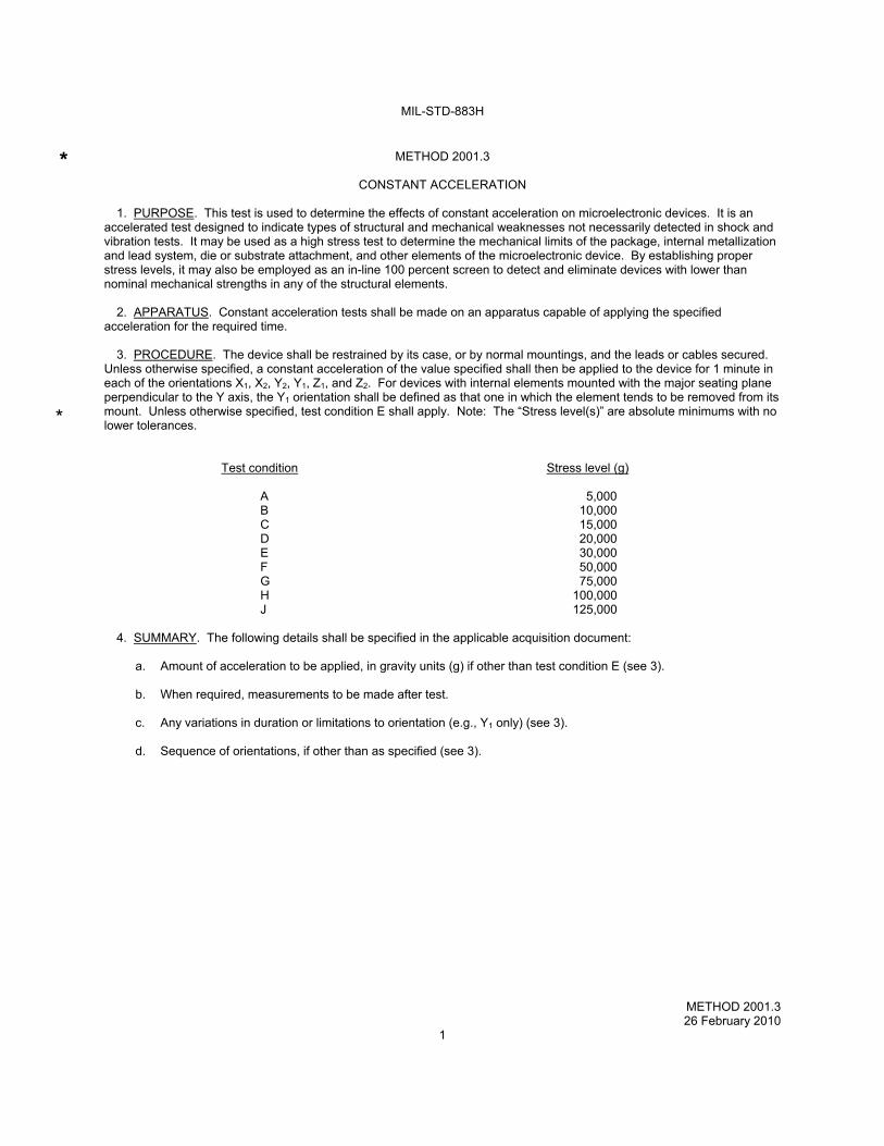
CONSTANT ACCELERATION 1. PURPOSE. This test is used to determine the effects of constant acceleration on microelectronic devices. It is an accelerated test designed to indicate types of structural and mechanical weaknesses not necessarily detected in shock and vibration tests. It may be used as a high stress test to determine the mechanical limits of the package, internal metallization and lead system, die or substrate attachment, and other elements of the microelectronic device. By establishing proper stress levels, it may also be employed as an in-line 100 percent screen to detect and eliminate devices with lower than nominal mechanical strengths in any of the structural elements. 2. APPARATUS. Constant acceleration tests shall be made on an apparatus capable of applying the specified acceleration for the required time. 3. PROCEDURE. The device shall be restrained by its case, or by normal mountings, and the leads or cables secured. Unless otherwise specified, a constant acceleration of the value specified shall then be applied to the device for 1 minute in each of the orientations X1, X2, Y2, Y1, Z1, and Z2. For devices with internal elements mounted with the major seating plane perpendicular to the Y axis, the Y1 orientation shall be defined as that one in which the element tends to be removed from its mount. Unless otherwise specified, test condition E shall apply. Note: The “Stress level(s)” are absolute minimums with no lower tolerances. Test condition Stress level (g) A 5,000 B 10,000 C 15,000 D 20,000 E 30,000 F 50,000 G 75,000 H 100,000 J 125,000 4. SUMMARY. The following details shall be specified in the applicable acquisition document: a. Amount of acceleration to be applied, in gravity units (g) if other than test condition E (see 3). b. When required, measurements to be made after test. c. Any variations in duration or limitations to orientation (e.g., Y1 only) (see 3). d. Sequence of orientations, if other than as specified (see 3).
*
*
MIL-STD-883H
METHOD 2001.3 26 February 2010
2
This page intentionally left blank
MIL-STD-883H
METHOD 2002.5 26 February 2010
1
METHOD 2002.5
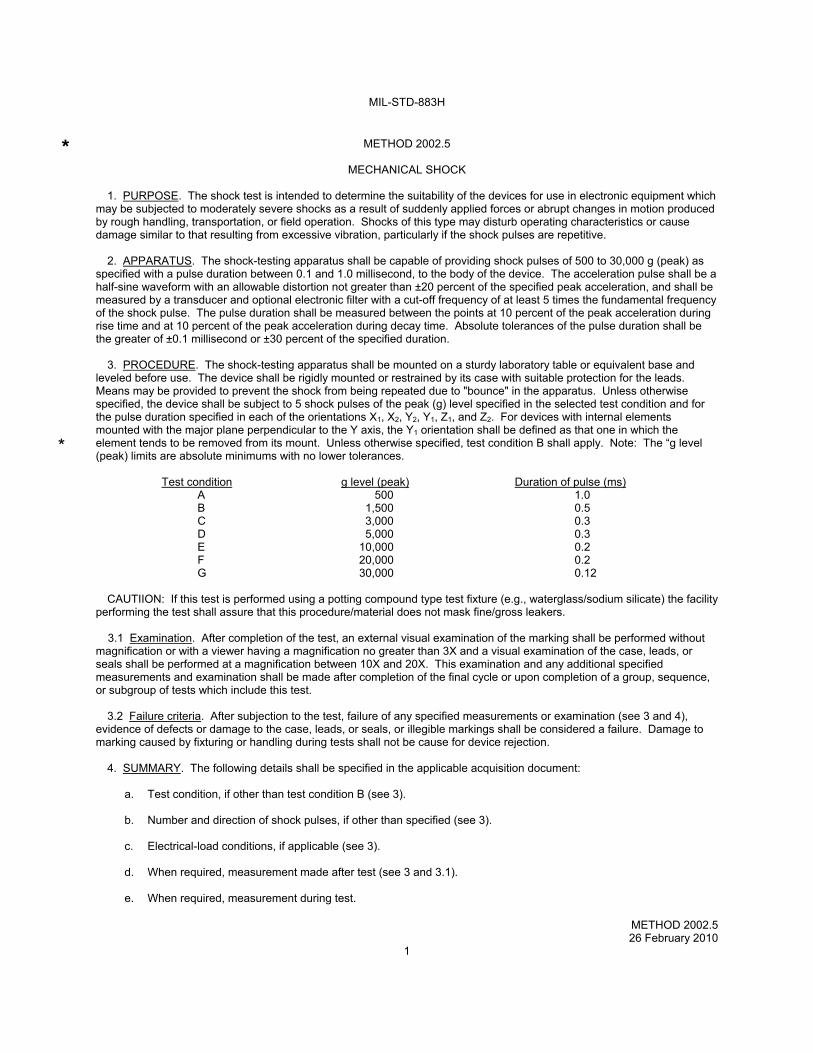
MECHANICAL SHOCK 1. PURPOSE. The shock test is intended to determine the suitability of the devices for use in electronic equipment which may be subjected to moderately severe shocks as a result of suddenly applied forces or abrupt changes in motion produced by rough handling, transportation, or field operation. Shocks of this type may disturb operating characteristics or cause damage similar to that resulting from excessive vibration, particularly if the shock pulses are repetitive. 2. APPARATUS. The shock-testing apparatus shall be capable of providing shock pulses of 500 to 30,000 g (peak) as specified with a pulse duration between 0.1 and 1.0 millisecond, to the body of the device. The acceleration pulse shall be a half-sine waveform with an allowable distortion not greater than ±20 percent of the specified peak acceleration, and shall be measured by a transducer and optional electronic filter with a cut-off frequency of at least 5 times the fundamental frequency of the shock pulse. The pulse duration shall be measured between the points at 10 percent of the peak acceleration during rise time and at 10 percent of the peak acceleration during decay time. Absolute tolerances of the pulse duration shall be the greater of ±0.1 millisecond or ±30 percent of the specified duration. 3. PROCEDURE. The shock-testing apparatus shall be mounted on a sturdy laboratory table or equivalent base and leveled before use. The device shall be rigidly mounted or restrained by its case with suitable protection for the leads. Means may be provided to prevent the shock from being repeated due to "bounce" in the apparatus. Unless otherwise specified, the device shall be subject to 5 shock pulses of the peak (g) level specified in the selected test condition and for the pulse duration specified in each of the orientations X1, X2, Y2, Y1, Z1, and Z2. For devices with internal elements mounted with the major plane perpendicular to the Y axis, the Y1 orientation shall be defined as that one in which the element tends to be removed from its mount. Unless otherwise specified, test condition B shall apply. Note: The “g level (peak) limits are absolute minimums with no lower tolerances. Test condition g level (peak) Duration of pulse (ms) A 500 1.0 B 1,500 0.5 C 3,000 0.3 D 5,000 0.3 E 10,000 0.2 F 20,000 0.2 G 30,000 0.12 CAUTIION: If this test is performed using a potting compound type test fixture (e.g., waterglass/sodium silicate) the facility performing the test shall assure that this procedure/material does not mask fine/gross leakers.
3.1 Examination. After completion of the test, an external visual examination of the marking shall be performed without magnification or with a viewer having a magnification no greater than 3X and a visual examination of the case, leads, or seals shall be performed at a magnification between 10X and 20X. This examination and any additional specified measurements and examination shall be made after completion of the final cycle or upon completion of a group, sequence, or subgroup of tests which include this test. 3.2 Failure criteria. After subjection to the test, failure of any specified measurements or examination (see 3 and 4), evidence of defects or damage to the case, leads, or seals, or illegible markings shall be considered a failure. Damage to marking caused by fixturing or handling during tests shall not be cause for device rejection. 4. SUMMARY. The following details shall be specified in the applicable acquisition document: a. Test condition, if other than test condition B (see 3). b. Number and direction of shock pulses, if other than specified (see 3). c. Electrical-load conditions, if applicable (see 3). d. When required, measurement made after test (see 3 and 3.1). e. When required, measurement during test.
*
*
MIL-STD-883H
METHOD 2002.5 26 February 2010
2
This page intentionally left blank
MIL-STD-883H
METHOD 2003.9 26 February 2010
1
METHOD 2003.9
SOLDERABILITY
1. Purpose. The purpose of this test method is to provide a referee condition for the evaluation of the solderability of terminations (including leads up to 0.125 inch in diameter) that will be assembled using tin lead eutectic solder. This evaluation is made on the basis of the ability of these terminations to be wetted and to produce a suitable fillet when coated by tin lead eutectic solder. These procedures will test whether the packaging materials and processes used during the manufacturing operations process produce a component that can be successfully soldered to the next level assembly using tin lead eutectic solder. A preconditioning test is included in this test method, which degrades the termination finish to provide a guard band against marginal finishes.
2. Procedure. The solderability test shall be performed in accordance with IPC/EIA J-STD-002 (current revision) “Solderability Tests for Component Leads, Terminations, Lugs Terminals and Wires”, and herein. The following details and exceptions shall apply:
2.1. Contractual Agreement. The contractual agreements statement in J-STD-002 shall not apply. Any exceptions to the requirements specified in J-STD-002 current revision and this test method shall be documented in the individual military procurement document or approved by the procuring military activity.
2.2. Coating Durability. The coating durability category (from J-STD-002 current revision) shall be as follows:
a. Category 2 – All non-tin component finishes, excluding gold (1 hr steam preconditioning).
b. Category 3 – For all other component finishes, including gold (8 hours + 15 minutes steam preconditioning).
2.3. Test Method. The test method from J-STD-002 (current revision shall be used as follows):
Test A – For through hole mount and surface mount leaded components, solid wire less than 0.045 inch diameter and stranded wire 18 AWG or smaller. If not otherwise specified in the procurement document, angle of immersion for surface mount leaded components shall be 90 degrees.
Test B – For surface mount leadless components.
Test C – For lugs, tabs, terminals, solid wires greater than 0.045-inch diameter, and stranded wires greater than 18
AWG.
2.3.1. Solder dipping of gold plated terminations. Gold plated terminations shall be cycled twice in flux and solder using one or two solder pots. The first immersion is to scavenge the gold on the terminations. It is recommended that a separate solder pot be used for gold plated devices. In any case, the user of this test should use two separate pots, a sufficiently large pot, or monitor closely the contamination level of a single small pot to assure that the test is performed as intended.
NOTE: For the purposes of testing under this method, the term “all leads” referred to in the accept/reject criteria imposed by J-STD-002 applies only to the actual leads used for the sample size and not to all the leads of the devices from which the sample is taken from.
3. Summary. The following details shall be specified in the applicable procurement document:
a. Depth of immersion if other than specified.
b. Angle of immersion for surface mount leaded components, if other than 90 degrees.
c. Measurements after test, where applicable.
*
*
*
MIL-STD-883H
METHOD 2003.9 26 February 2010
2
This page intentionally left blank.
MIL-STD-883H
METHOD 2004.6 26 February 2010
1
METHOD 2004.6
LEAD INTEGRITY
1. PURPOSE. This method provides various tests for determining the integrity of microelectronic device leads (terminals), welds, and seals. Test condition A provides for straight tensile loading. Test condition B1 provides for application of bending stresses to determine integrity of leads, seals, and lead plating while B2 employs multiple application of bending stresses primarily to determine the resistance of the leads to metal fatigue under repeated bending. Test conditions C1 and C2 provide for application of torque or twisting stresses to device leads or studs, respectively, to determine integrity of leads and seals. Test condition D provides for application of peel and tensile stresses to determine integrity of terminal adhesion and plating of leadless packages. It is recommended that this test be followed by a seal test in accordance with method 1014 to determine any effect of the stresses applied on the seal as well as on the leads (terminals).
2. APPARATUS. See applicable test condition.
3. GENERAL PROCEDURE APPLICABLE TO ALL TEST CONDITIONS. The device shall be subjected to the stresses described in the specified test condition and the specified end-point measurements and inspections shall be made except for initial conditioning or unless otherwise specified. Unless otherwise specified, the Sample Size Series sampling shall apply to the leads, terminals, studs or pads chosen from a minimum of 3 devices.
4. SUMMARY. The following details and those required by the specific test condition shall be specified in the applicable acquisition document: a. Test condition letter. b. Number and selection of leads (terminals), if different from above.
TEST CONDITION A - TENSION
1. PURPOSE. This test is designed to check the capabilities of the device leads, welds, and seals to withstand a straight pull.
2. APPARATUS. The tension test requires suitable clamps and fixtures for securing the device and attaching the specified weight without lead restriction. Equivalent linear pull test equipment may be used.
3. PROCEDURE. A tension of 0.227 kg (8 ounces), unless otherwise specified, shall be applied, without shock, to each
lead or terminal to be tested in a direction parallel to the axis of the lead or terminal and maintained for 30 seconds minimum. The tension shall be applied as close to the end of the lead (terminal) as practicable.
3.1 Failure criteria. When examined using 10X magnification after removal of the stress, any evidence of breakage, loosening, or relative motion between the lead (terminal) and the device body shall be considered a failure. When a seal test in accordance with method 1014 is conducted as a post test measurement following the lead integrity test(s), meniscus cracks shall not be cause for rejection of devices which pass the seal test.
4. SUMMARY. The following details shall be specified in the applicable acquisition document: a. Weight to be attached to lead, if other than .227 kg (8 ounces) (see 3). b. Length of time weight is to be attached, if other than 30 seconds (see 3).
TEST CONDITION B1 - BENDING STRESS
1. PURPOSE. This test is designed to check the capability of the leads, lead finish, lead welds, and seals of the devices to withstand stresses to the leads and seals which might reasonably be expected to occur from actual handling and assembly of the devices in application, or to precondition the leads with a moderate bending stress prior to environmental testing.
2. APPARATUS. Attaching devices, clamps, supports, or other suitable hardware necessary to apply the bending stress through the specified bend angle.
*
MIL-STD-883H
METHOD 2004.6 26 February 2010
2
3. PROCEDURE. Each lead or terminal to be tested shall be subjected to force sufficient to bend the lead as specified in 3.1 through 3.5, as applicable. Any number or all of the leads of the test device may be bent simultaneously. Rows of leads may be bent one row at a time. Each lead shall be bent through one cycle as follows: Bend through the specified arc in one direction and return to the original position. All arcs shall be made in the same plane without lead restriction.
3.1 Direction of bends. Test leads shall be bent in the least rigid direction. If there is no least rigid direction, they may be bent in any direction. No lead shall be bent so as to interfere with another lead. If interference is unavoidable, the test lead shall be bent in the opposite direction to the angle specified and returned to its normal position.
3.2 Procedure for initial conditioning of formed leads. When normally straight leads are supplied in a formed condition (including the staggered lead dual-in- line configuration), the lead forming operation shall be considered acceptable initial conditioning in place of that specified, provided the lead forming has been done after lead plating and the forming is at least as severe in permanent lead deformation as the specified bending.
3.3 Procedure for flexible and semi-flexible leads (e.g., flat packs and axial-lead metal-can devices).
3.3.1 Flexible leads. A lead shall be considered flexible if its section modulus (in the least rigid direction) is less than or equal to that of a rectangular lead with a cross section of 0.15 x 0.51 mm (.006 x .020 inch). Round leads less than or equal to 0.51 mm (.020 inch) in diameter shall be considered flexible. Flexible leads shall be bent through an arc of at least 45° measured at a distance 3.05 ±.76 mm (0.120 ±0.03 inch) along the lead from the seal unless otherwise specified.
3.3.2 Semi-flexible leads. Semi-flexible leads are those leads with a section modulus (in the least rigid direction) greater than that of a rectangular lead with a cross section of 0.15 x 0.51 mm (0.006 x 0.020 inch) which are intended to be bent during insertion or other application. Round leads greater than 0.51 mm (.020 inch) diameter shall be considered semi-flexible except as noted in 3.5. Semi-flexible leads shall be bent through an arc of at least 30° measured at the lead extremities unless otherwise specified.
3.4 Procedure for dual-in-line and pin grid array package leads. Dual-in-line package leads are leads with more than one section modulus, with leads normally aligned in parallel at a 90° angle from the bottom of the package during insertion. Dual-in-line package leads shall be bent inward through an angle sufficient to cause the lead to retain a permanent bend (i.e., after stress removal) of at least 15°. For configuration 1 and 2, the angle of bend shall be measured from the lead extremities to the first bend (see figure 2004-1). For configuration 3, the angle of bend shall be measured from the lead extremities to the seating plane (see figure 2004-1). Pin grid array packages shall have the leads required for testing from the outside row of leads on opposite sides bent through an angle sufficient to cause the lead to retain a permanent bend (i.e., after stress removal) of at least 15°. The angle of bend shall be 15° from normal and the bend shall be made at the approximate seating plane. At the completion of the initial bend, the leads shall be returned to their approximate original position.
3.5 Procedure for rigid leads or terminals. A lead or terminal shall be considered rigid if it is not intended to be flexed in mounting, and not covered in 3.3 or 3.4. Devices with terminals complying with this description shall be subjected to a normal mounting operation and removal, unless otherwise specified. When the normal mounting/removal operation is destructive to the terminals (e.g., terminal weld, wire wrap), the initial conditioning need not be performed.
3.6 Failure criteria. When examined using magnification between 10X and 20X after removal of the stress, any evidence of breakage, loosening, or relative motion between the terminal lead and the device body shall be considered a device failure. When specified, post-test measurements (see 4) shall be made after visual examination. When the above procedures are used as initial conditioning in conjunction with other tests, these measurements may be conducted at the conclusion of that test or sequence of tests.
4. SUMMARY. The following details shall be specified in the applicable acquisition document: a. Bending arc, if other than that specified. b. Procedure, if other than that specified. c. Number and selection of leads and procedure for identification, if other than that specified.
d. Post test measurements, if applicable (see 3.6)
MIL-STD-883H
METHOD 2004.6 26 February 2010
3
TEST CONDITION B2 - LEAD FATIGUE
1. PURPOSE. This test is designed to check the resistance of the leads to metal fatigue.
2. APPARATUS. Attaching devices, clamps, supports, or other suitable hardware necessary to apply a repeated bending stress through the specified bend angle.
3. PROCEDURE. The appropriate procedure of 3.1 or 3.2 for the device under test shall be used.
3.1 Procedure for dual-in-line packages. The leads to be tested shall be subjected to three cycles of test condition B1 and shall be subjected to a force sufficient to bend the leads as specified in 3.4 of condition B1. 3.2 Procedure for flat packages and can packages. A force of 0.229 ±0.014 kg (8 ±0.5 ounces), unless otherwise specified, shall be applied to each lead to be tested for three 90° ±5° arcs of the case. For leads with a preplated or prefinished section modulus equal to or less than that of a rectangular lead with a cross section of 0.16 x 0.51 mm (0.006 x 0.020 inches) or round leads with a cross section of 0.51 mm (0.020 inch) in diameter, the force shall be 0.085 ±0.009 kg (3 ±0.3 ounces). Section modulus is defined as bc2/6 for rectangular leads, and 0.098 (b1)
3 for round leads (see MIL-STD-1835). An arc is defined as the movement of the case, without torsion, to a position perpendicular to the pull axis and return to normal. All arcs on a single lead shall be made in the same direction and in the same plane without lead restriction. A bending cycle shall be completed in from 2 to 5 seconds. For devices with rectangular or ribbon leads, the plane of the arcs shall be perpendicular to the flat plane of the lead. The test shall not be applied to end leads of packages where its application will apply primarily torsion forces at the lead seal.
3.2.1 Optional procedure for fine pitch/small leads. A force as determined by the following formula, unless otherwise specified, shall be applied to each lead to be tested for 90 degrees ±5 degree arcs of the device. All other conditions of section 3.2 shall apply: Weight = (area in square inches) x 2.1 % x (K psi) x 453.6 grams/lb, where K is based on the ultimate tensile strength (UTS) for a particular material. Typical values for kovar and alloy 42 are listed below. The UTS for other materials can be found in vendor data sheets. The result shall be rounded to the nearest whole number.
NOTE: A lead pitch of less than or equal to 25 mils is considered fine pitch.
Material UTS in psi
Kovar Alloy 42
75000 71000
3.3. Failure criteria. A broken lead on a device shall be considered a failure. When examined using magnification between 10X and 20X after removal of the stress, any device which exhibits any evidence of breakage, loosening, or relative motion between the terminal lead and the device body shall be considered a device failure.
4. SUMMARY. The following details shall be specified in the applicable acquisition document: a. Force to be applied to the lead, if other than above (see 3). b. Number of cycles, if other than above (see 3). c. Maximum bend angle, if other than above (see 3).
*
*
MIL-STD-883H
METHOD 2004.6 26 February 2010
4
TEST CONDITION C1 - LEAD TORQUE
1. PURPOSE. This test is designed to check device leads (or terminals) and seals for their resistance to twisting
motions.
2. APPARATUS. The torque test requires suitable clamps and fixtures, and a torsion wrench or other suitable method of applying the specified torque without lead restriction.
3. PROCEDURE. The appropriate procedure of 3.1 or 3.2 for the device under test shall be used.
3.1 Procedure for devices with circular cross-section terminals or leads. The device body shall be rigidly held and the specified torque shall be applied for 15 seconds minimum to the lead (terminal) to be tested, without shock, about the axis of the lead (terminal).
3.2 Procedure for devices with rectangular cross-section terminals or leads. The device body shall be rigidly held and a torque of 1.45 ±.145 kg-mm (2.0 ±0.2 ounce-inch) unless otherwise specified, shall be applied to the lead (terminal) at a distance of 3.05 ±0.76 mm (0.12 ±0.03 inch) from the device body or at the end of the lead if it is shorter than 3.05 mm (0.12 inch). The torque shall be applied about the axis of the lead once in each direction (clockwise and counterclockwise). When devices have leads which are formed close to the body, the torque may be applied 3.05 ±0.76 mm (0.12 ±0.03 inch) from the form. For device leads which twist noticeably when less than the specified torque is applied, the twist shall be continued until the twist angle reaches 30° ±10° or the specified torque is achieved, whichever condition occurs first. The lead shall then be restored to its original position.
3.3 Failure criteria. When examined using magnification between 10X and 20X after removal of the stress, any evidence of breakage, loosening, or relative motion between the terminal (lead) and the device body shall be considered a device failure. When a seal test in accordance with method 1014 is conducted as a post test measurement following the lead integrity test(s), meniscus cracks shall not be cause for rejection of devices which pass the seal test.
4. SUMMARY. The following details shall be specified in the applicable acquisition document: a. Torque to be applied for circular cross-section leads (see 3.1). b. Duration of torque application for circular cross-section leads, if other than 15 seconds minimum (see 3.1). c. Torque to be applied for rectangular cross-section leads, if other than 1.45 ±0.145 kg-mm (2.0 ±0.2 ounce-inch)
(see 3.2). d. See general summary above.
TEST CONDITION C2 - STUD TORQUE
1. PURPOSE. This test is designed to check the resistance of the device with threaded mounting stud to the stress caused by tightening the device when mounting.
2. APPARATUS. The torque test requires suitable clamps and fixtures, and a torsion wrench or suitable method of applying the specified torque.
3. PROCEDURE. The device shall be clamped by its body or flange. A flat steel washer of a thickness equal to six thread pitches of the stud being tested and a new class 2 fit steel nut shall be assembled in that order on the stud, with all parts clean and dry. The specified torque shall be applied without shock to the nut for the specified period of time. The nut and washer shall then be disassembled from the device, and the device then examined for compliance with the requirements.
MIL-STD-883H
METHOD 2004.6 26 February 2010
5
3.1 Failure criteria. The device shall be considered a failure if any of the following occurs: a. The stud breaks or is elongated greater than one-half of the thread pitch. b. It fails the specified post-test end point measurements. c. There is evidence of thread stripping or deformation of the mounting seat.
4. SUMMARY. The following details shall be specified in the applicable acquisition document: a. The amount of torque to be applied (see 3). b. Length of time torque is to be applied (see 3). c. Measurements to be made after test (see 3).
TEST CONDITION D - SOLDER PAD ADHESION FOR LEADLESS CHIP CARRIER AND SIMILAR DEVICES
1. PURPOSE. This test is designed to check the capabilities of the device solder pads to withstand a delamination (peel) stress of specified tension and time.
2. APPARATUS. Equipment for 10X magnification, suitable clamps and fixtures for securing the device and applying the specified tension/time conditions to wires soldered to the device solder pads. Equivalent linear pull test equipment may be used.
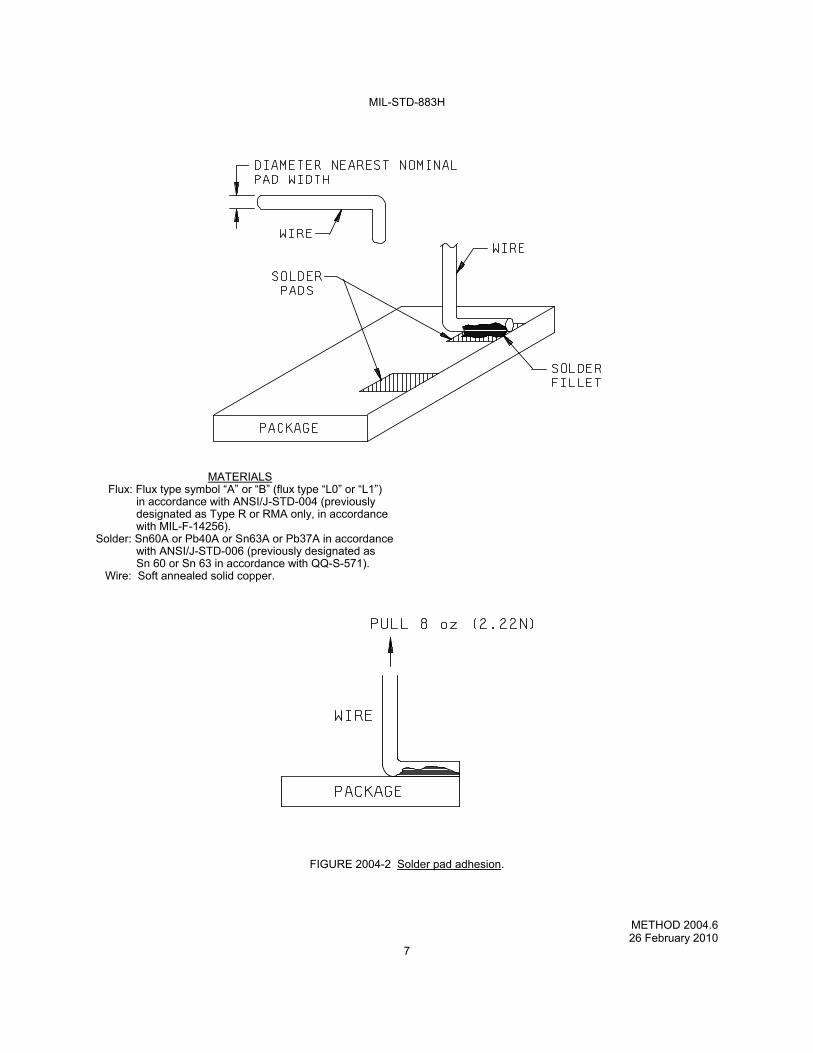
3. PROCEDURE. Unless otherwise specified, a delamination (peel) stress test shall be applied to randomly selected solder pads from each device selected for test. Further, unless otherwise specified, the sampling shall be Sample Size Number = 15, c = 0 based on the number of solder pads tested, chosen from a minimum of three devices. Preparation and testing of devices shall be in accordance with figure 2004-2 of this method and as follows.
a. Pretinned soft annealed solid copper wire of a gauge (diameter) nearest, but not exceeding that of the nominal solder pad width, shall be soldered using Sn60A or Pb40A or Sn63A or Pb37A of ANSI/J-STD-006 (previously known as Sn60 or Sn63 solder in accordance with QQ-S-571) to each solder pad to be tested in a manner such that the wire is bonded over the entire solder pad length and terminates at the package edge (see figure 2004-2). The unsoldered portion of the wire shall be bent perpendicular to the bond plane prior to attachment. Caution should be taken to assure that the solder pad metallization is not damaged during the soldering or the wire bending operation.
b. Unless otherwise specified, a minimum tension of 8 ounces (2.22 N) shall be applied, without shock, to each
solder pad to be tested in a direction perpendicular to the solder pad surface and maintained for 30 seconds minimum.
3.1 Failure criteria. When examined, using 10X magnification, after removal of the tension stress, the appearance of any
delamination involving constituent solder pad interfaces shall be considered an adhesion failure of the solder pad. Separation of the solder pad from the device is an obvious (without visual magnification) adhesion failure. Separation of the wire from the solder fillet (leaving the solder pad intact) or wire breakage is considered a test procedure failure.
4. SUMMARY. The following details shall be specified in the applicable acquisition document: a. Sampling criteria, if other than specified (see 3.1). b. Failure criteria, if other than specified (see 3.1). c. Tension to be applied in this test if other than 8 ounces (2.22 N).
d. Length of time tension is to be applied if other than 30 seconds.
MIL-STD-883H
METHOD 2004.6 26 February 2010
6
FIGURE 2004-1 Angle of bend for dual-in-line package configurations.
MIL-STD-883H
METHOD 2004.6 26 February 2010
7
MATERIALS Flux: Flux type symbol “A” or “B” (flux type “L0” or “L1”) in accordance with ANSI/J-STD-004 (previously designated as Type R or RMA only, in accordance with MIL-F-14256). Solder: Sn60A or Pb40A or Sn63A or Pb37A in accordance with ANSI/J-STD-006 (previously designated as Sn 60 or Sn 63 in accordance with QQ-S-571). Wire: Soft annealed solid copper.
FIGURE 2004-2 Solder pad adhesion.

MIL-STD-883H
METHOD 2004.6 26 February 2010
8
This page intentionally left blank
MIL-STD-883H
METHOD 2005.2 15 August 1984
1
METHOD 2005.2
VIBRATION FATIGUE
1. PURPOSE. The purpose of this test is to determine the effect on the device of vibration in the frequency range specified.
2. APPARATUS. Apparatus for this test shall include equipment capable of providing the sustained vibration within the specified levels and the necessary optical and electrical equipment to conduct post-test measurements.
3. PROCEDURE. The device shall be rigidly fastened on the vibration platform and the leads or cables adequately secured. The device shall be vibrated with a constant amplitude simple harmonic motion having a peak acceleration corresponding to the specified test condition. For test condition A, constant amplitude harmonic motion in the range of 60 ±20 Hz having an amplitude of 0.06 inch double amplitude (total excursion) shall be acceptable as an alternative to the specified peak acceleration. The vibration shall be applied for 32 ±8 hours minimum, in each of the orientations X, Y, and Z for a total of 96 hours, minimum. When specified, devices with an internal cavity containing parts or elements subject to possible movement or breakage during vibration shall be further examined by radiographic examination in accordance with method 2012 or by delidding or opening and internal visual examination at 30X magnification to reveal damage or dislocation. Where this test is performed as part of a group or subgroup of tests, the post-test measurements or inspections need not be performed specifically at the conclusion of this test, but may be performed once at the conclusion of the group or subgroup. Test condition Peak acceleration, g A 20 B 50 C 70
3.1 Examination. After completion of the test, an external visual examination of the marking shall be performed without magnification or with a viewer having a magnification no greater than 3X and a visual examination of the case, leads, or seals shall be performed at a magnification between 10X and 20X. This examination and any additional specified measurements and examination shall be made after completion of the final cycle or upon completion of a group, sequence, or subgroup of tests which include this test.
3.2 Failure criteria. After subjection to the test, failure of any specified measurement or examination (see 3 and 4), evidence of defects or damage to the case, leads, or seals, or illegible markings shall be considered a failure. Damage to marking caused by fixturing or handling during tests shall not be cause for device rejection.
3.3 Test frequency and amplitude. For test condition A, B, or C, the double amplitude and frequency used shall result in the application of the peak accelerations of 20, 50, or 70 g's. Peak acceleration may be computed using the following equation: g = A (F)2 (2) (386) Where: A = double amplitude in inches. F = frequency in radians/second.
4. SUMMARY. The following details shall be specified in the applicable acquisition document: a. Test condition (see 3). b. Test frequency and test double amplitude (see 3 and 3.3), if other than specified. c. Test time and specimen orientation, if other than specified (see 3). d. Measurements after test (see 3 and 3.1).

MIL-STD-883H
METHOD 2005.2 15 August 1984
2
This page intentionally left blank
MIL-STD-883H
METHOD 2006.1 31 August 1977
1
METHOD 2006.1
VIBRATION NOISE
1. PURPOSE. The purpose of this test is to measure the amount of electrical noise produced by the device under vibration.
2. APPARATUS. Apparatus for this test shall include equipment capable of providing the required variable frequency vibration at the specified levels, a calibrated high impedance voltmeter for noise measurement during test and the necessary optical and electronic equipment for post-test measurements.
3. PROCEDURE. The device and its leads shall be rigidly fastened on the vibration platform and the leads or cables adequately secured. The device shall be vibrated with simple harmonic motion having either an amplitude of 0.06 inch double amplitude (maximum total excursion) or a constant peak acceleration of 20 g minimum. The vibration frequency shall be varied approximately logarithmically between 20 and 2,000 Hz. The entire frequency range shall be traversed in not less than 4 minutes for each cycle. This cycle shall be performed once in each of the orientations X, Y, and Z (total of 3 times), so that the motion shall be applied for a total period of approximately 12 minutes. The specified voltages and currents shall be applied in the test circuit. The maximum noise-output voltage across the specified load resistance during traverse, shall be measured with an average-responding root-mean-square (rms) calibrated high impedance voltmeter. The meter shall measure, with an error of not more than 3 percent, the rms value of a sine-wave voltage at 2,000 Hz. The characteristic of the meter over a bandwidth of 20 to 2,000 Hz shall be ±1 decibel (dB) of the value at 2,000 Hz, with an attenuation rate below 20 and above 20,000 Hz of 6 ±2 dB per octave. The maximum inherent noise in the circuit shall be at least 10 dB below the specified noise-output voltage. When specified, devices with an internal cavity containing parts or elements subject to possible movement or breakage during vibration shall be further examined by radiographic examination in accordance with method 2012 or by delidding or opening and internal visual examination at 30X magnification to reveal damage or dislocation. Where this test is performed as part of a group or subgroup of tests, the post-test measurements or inspections need not be performed specifically at the conclusion of this test, but may be performed once at the conclusion of the group or subgroup.
3.1 Examination. After completion of the test, an external visual examination of the marking shall be performed without magnification or with a viewer having a magnification no greater than 3X and a visual examination of the case, leads, or seals shall be performed at a magnification between 10X and 20X. This examination and any additional specified measurements and examination shall be made after completion of the final cycle or upon completion of a group, sequence, or subgroup of tests which include this test.
3.2 Failure criteria. After subjection to the test, failure of any specified measurement or examination (see 3 and 4), evidence of defects or damage to the case, leads, or seals, or illegible markings shall be considered a failure. Damage to marking caused by fixturing or handling during tests shall not be cause for device rejection.
4. SUMMARY. The following details shall be specified in the applicable acquisition document: a. Test condition (see 3). b. Test voltages and currents (see 3). Unless otherwise specified, these shall be the nominal operating voltages and
currents for the device. c. Load resistance (see 3). Unless otherwise specified, this shall be the maximum rated operating load of the
device. d. Measurements after test (see 3 and 3.1). e. Noise-output voltage limit (see 3).

MIL-STD-883H
METHOD 2006.1 31 August 1977
2
This page intentionally left blank
MIL-STD-883H
METHOD 2007.3 24 August 1998
1
METHOD 2007.3
VIBRATION, VARIABLE FREQUENCY
1. PURPOSE. The variable frequency vibration test is performed for the purpose of determining the effect on component parts of vibration in the specified frequency range. This is a destructive test.
2. APPARATUS. Apparatus for this test shall include equipment capable of providing the required variable frequency vibration at the specified levels and the necessary optical and electrical equipment for post-test measurements.
3. PROCEDURE. The device shall be rigidly fastened on the vibration platform and the leads or cables adequately secured. The device shall be vibrated with simple harmonic motion having either a peak to peak amplitude of 0.06 inch (±10 percent) or a peak acceleration of the specified test condition A, B, or C (+20 percent, -0 percent g). Test conditions shall be amplitude controlled below the crossover frequency and g level controlled above. The vibration frequency shall be varied approximately logarithmically between 20 and 2,000 Hz. The entire frequency range of 20 to 2,000 Hz and return to 20 Hz shall be traversed in not less than 4 minutes. This cycle shall be performed 4 times in each of the orientations X, Y, and Z (total of 12 times), so that the motion shall be applied for a total period of not less than 48 minutes. When specified, devices with an internal cavity containing parts or elements subject to possible movement or breakage during vibration shall be further examined by radiographic examination in accordance with method 2012 or by delidding or opening and internal visual examination at 30X magnification to reveal damage or dislocation. Where this test is performed as part of a group or subgroup of tests, the post-test measurements or inspections need not be performed specifically at the conclusion of this test, but may be performed once at the conclusion of the group or subgroup. Test condition Peak acceleration, g A 20 B 50 C 70
CAUTION: If this test is performed using a potting compound type test fixture (e.g., waterglass/sodium silicate) the facility performing the test shall assure that this procedure/material does not mask fine/gross leakers.
3.1 Examination. After completion of the test, an external visual examination of the marking shall be performed without magnification or with a viewer having a magnification no greater than 3X and a visual examination of the case, leads, or seals shall be performed at a magnification between 10X and 20X. This examination and any additional specified measurements and examination shall be made after completion of the final cycle or upon completion of a group, sequence, or subgroup of tests which include this test.
3.2 Failure criteria. After subjection to the test, failure of any specified measurement or examination (see 3 and 4), evidence of defects or damage to the case, leads, or seals, or illegible markings shall be considered a failure. Damage to marking caused by fixturing or handling during tests shall not be cause for device rejection.
4. SUMMARY. The following details shall be specified in the applicable acquisition document:
a. Test condition (see 3). b. Measurements after test (see 3 and 3.1).
MIL-STD-883H
METHOD 2007.3 24 August 1998
2
This page intentionally left blank
MIL-STD-883H
METHOD 2008.1 31 August 1977
1
METHOD 2008.1
VISUAL AND MECHANICAL
Method 2008 is canceled effective 15 November 1974. It is superseded by methods 2014, 2015, and 2016. Test condition A of method 2008 is superseded by method 2016. Test condition B, except for 3.2.1 (Marking), is superseded by method 2014. Paragraph 3.2.1 is superseded by method 2015.
MIL-STD-883H
METHOD 2008.1 31 August 1977
2
This page intentionally left blank
MIL-STD-883H
METHOD 2009.10 26 February 2010
1
METHOD 2009.10
EXTERNAL VISUAL
1. PURPOSE. The purpose of this test method is to verify the workmanship of hermetically packaged devices. This test method shall also be utilized to inspect for damage due to handling, assembly, and/or test of the packaged device. This examination is normally employed at outgoing inspection within the device manufacturer's facility, or as an incoming inspection of the assembled device.
2. APPARATUS. Equipment used in this test shall be capable of demonstrating device conformance to the applicable requirements. Equipment shall include optical devices capable of magnification of at least 1.5X to 10X, with a relatively large and accessible field of view.
3. PROCEDURE
3.1 Magnification. Devices shall be examined at 1.5X to 10X magnification. Devices may be examined anywhere in the range of 1.5X to 10X, however, acceptable product must be capable of passing all criteria when examined at 10X magnification. Individual glass seals (see 3.3.8) shall be examined at 7X to 10X magnification.
3.2 Foreign material. When foreign material is present, and its adherence is in question, the device may be subjected to a clean filtered gas stream (vacuum or expulsion) of approximately 20 psig.
3.3 Failure criteria. Devices shall fail if they exhibit any of the following:
3.3.1 General
a. Illegible marking, or marking content or placement not in accordance with the applicable specification.
b. Presence of any secondary coating material that visually obscures a seal area(s) (i.e., any hermetic interface).
c. Evidence of any nonconformance with the detail drawing or applicable procurement document, or absence of any
required feature.
3.3.2 Foreign/displaced material
a. Braze material flow, or other foreign material (i.e., contamination or corrosion) that reduces the isolation between leads or between braze pads to less than 50% of the lead separation (pad separation for brazed leads) but in no case less than the case outline minimum.
b. Leads or terminals that are not free of foreign material such as paint or other adherent deposits.
3.3.3 Construction defects
a. Protrusions on the bottom (mounting) surface of the package that extend beyond the seating plane.
b. Protrusions (excluding glass run-out) on any other package surface that exceed the lead thickness in height
(leaded packages).
c. Protrusions on the lid or cover, or extending beyond the surface plane of solder pads, that exceed 25% of the terminal width in height (leadless packages).
d. Metallization not intended by design between solder pads, between elements of thermal patterns and/or between
seal ring or lid to metallized castellations that reduce the isolation to less than 50% of pad separation (leadless packages).
*
MIL-STD-883H
METHOD 2009.10 26 February 2010
2
3.3.4 Package Body/Lid Finish
a. Defective finish (peeling, flaking, pitting, blistering, or corrosion). Discoloration that does not exhibit these conditions is acceptable.
b. Scratches, mars, or indentations, either due to damage or processing, that expose base metal. Exposed
underplate is acceptable. 3.3.5 Leads
a. Broken leads.
b. Leads or terminals that are not intact or aligned in their normal location, free of sharp or unspecified lead bends, or
twisted more than 20° from the normal lead plane.
c. Leads with pits and/or depressions that exceed 25% of the width (diameter for round leads) and are greater than 50% of the lead thickness in depth.
d. Leads with burrs exceeding a height greater than 50% of the lead thickness.
e. Lead misalignment to the braze pad to the extent that less than 75% of the lead braze section is brazed to the pad.
f. Metallization (including solder lead finish) in which the isolation between leads or between lead and other package
metallization is reduced to less than 50% of lead separation (pad separation for brazed leads) but in no case less than the case outline minimum.
g. Braze material that increases the lead dimensions to greater than 1.5 times the lead thickness above the design
maximum between the seating plane and the ceramic body or that increases the lead dimensions to greater than the design maximum below the seating plane.
h. Scratches that expose base metal over more than 5% of the lead surface area. Exposed base metal on the cut
lead ends is acceptable and does not count in the 5%.
3.3.6 Ball/column grid array leads.
a. Nonconformance with any design criteria (see 3.3.1.c herein). b. Solder columns/spheres off the edge of the pad by more than 10% of the column diameter. c. Broken, twisted or damaged solder columns/spheres. Damaged columns/spheres (scored, gouged) that fail to
meet final dimensional requirements. d. Solder column bends or misalignments that do not meet the drawing design criteria. e. Solder columns/spheres containing any hole, pit, gouge or depression greater than 30% of the column/sphere
diameter or, any vertical voids going the entire length of the column/sphere.
*
MIL-STD-883H
METHOD 2009.10 26 February 2010
3
f. Solder columns/spheres containing surface cracks greater than 30% of the column/sphere diameter or any
cracking of indeterminate measure. g. Columns/spheres with burrs or bumps exceeding 20% of the column/sphere diameter. h. Columns/spheres that exhibit peeling, flaking, or blistering. i. Solder column fillets that exhibit any of the following: i. Voids, holes, and/or pits greater than 15% of the fillet surface area. ii. Incomplete reflow as shown by poor wetting. iii. Coverage less than 75% around the column circumference. iv. Height less than 50% of the column diameter (for at least 75% of the column circumference). j. Dewetting or non-wetting of columns greater than 5% of the column surface area.
k. For copper reinforced columns that exhibit any of the following: i. Copper ribbon delamination exceeding 25% around the column circumference. ii Exposed copper greater than 5% of the column surface area. Exposed (cut) copper on the free end of the
column is acceptable and does not count in the 5%.
l. Discoloration of columns/spheres due to corrosion, crusting, or residual flux. Evidence of flux residue, stains, rust, or signs of corrosion that can be seen without magnification (1X).
m. Foreign material, discoloration, or adherent deposits within 0.5 mm of the free end of the column as these may
cause solderability problems. n. Solder columns/spheres that do not meet requirements for device co-planarity/uniformity of the drawing design
criteria (typically < 150 μm).
3.3.7 Package body/lid - leaded devices
a. Broken packages or cracks in the packages. Surface scratches shall not be cause for failure except where they
violate other criteria stated herein for marking, finish, etc.
b. Any chipout dimension that exceeds 0.060 inch in any direction on the surface and has a depth that exceeds 25% of the thickness of the affected package element (e.g., cover, base, or wall).
c. External lead metallization stripe forming a conductor to a brazed lead that exhibits voids greater than 25% of the
conductor width.
d. Evidence of cracks, delamination, separation, or voiding on any multilayer ceramic package.
*
MIL-STD-883H
METHOD 2009.10 26 February 2010
4
3.3.8 Package body/lid - leadless devices
a. Ceramic chip-outs that dimensionally exceed 50% of the distance between terminals in any direction on the
affected surface (edge or corner), and exceed a depth of 25% of the thickness of the affected package element (e.g., cover, lid, base, or wall).
b. Evidence of cracks, delamination, separation, or voiding on any package element.
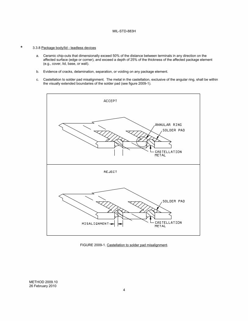
c. Castellation to solder pad misalignment. The metal in the castellation, exclusive of the angular ring, shall be within
the visually extended boundaries of the solder pad (see figure 2009-1).
FIGURE 2009-1. Castellation to solder pad misalignment.
*
MIL-STD-883H
METHOD 2009.10 26 February 2010
5
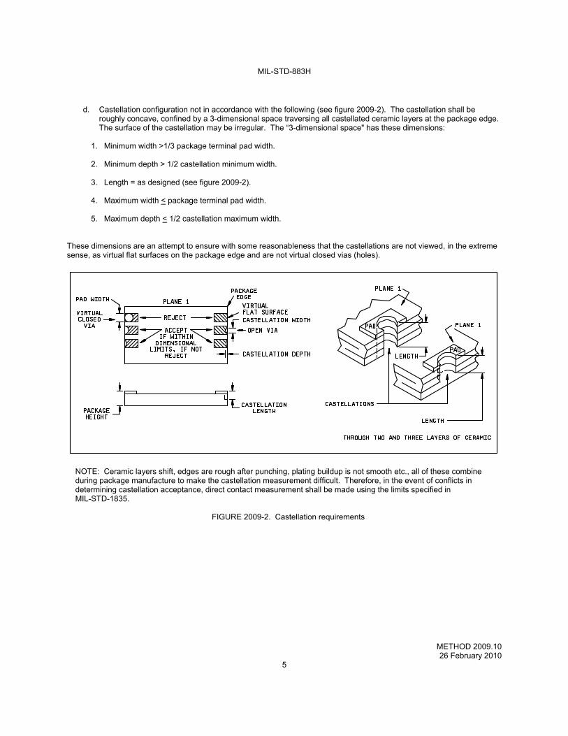
d. Castellation configuration not in accordance with the following (see figure 2009-2). The castellation shall be
roughly concave, confined by a 3-dimensional space traversing all castellated ceramic layers at the package edge. The surface of the castellation may be irregular. The “3-dimensional space" has these dimensions:
1. Minimum width >1/3 package terminal pad width.
2. Minimum depth > 1/2 castellation minimum width.
3. Length = as designed (see figure 2009-2).
4. Maximum width < package terminal pad width.
5. Maximum depth < 1/2 castellation maximum width.
These dimensions are an attempt to ensure with some reasonableness that the castellations are not viewed, in the extreme sense, as virtual flat surfaces on the package edge and are not virtual closed vias (holes).
NOTE: Ceramic layers shift, edges are rough after punching, plating buildup is not smooth etc., all of these combine during package manufacture to make the castellation measurement difficult. Therefore, in the event of conflicts in determining castellation acceptance, direct contact measurement shall be made using the limits specified in MIL-STD-1835.
FIGURE 2009-2. Castellation requirements
MIL-STD-883H
METHOD 2009.10 26 February 2010
6
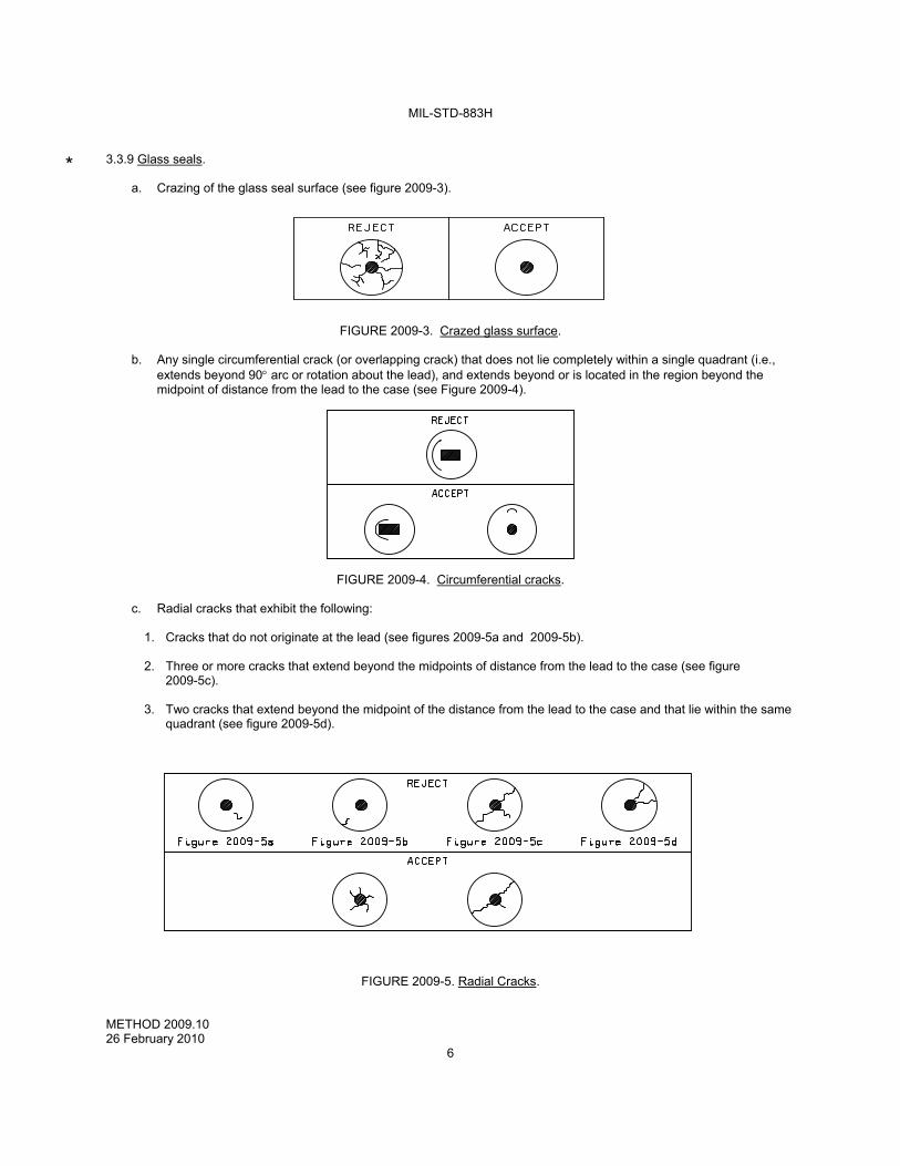
3.3.9 Glass seals.
a. Crazing of the glass seal surface (see figure 2009-3).
FIGURE 2009-3. Crazed glass surface.
b. Any single circumferential crack (or overlapping crack) that does not lie completely within a single quadrant (i.e., extends beyond 90 arc or rotation about the lead), and extends beyond or is located in the region beyond the midpoint of distance from the lead to the case (see Figure 2009-4).
FIGURE 2009-4. Circumferential cracks.
c. Radial cracks that exhibit the following:
1. Cracks that do not originate at the lead (see figures 2009-5a and 2009-5b). 2. Three or more cracks that extend beyond the midpoints of distance from the lead to the case (see figure
2009-5c). 3. Two cracks that extend beyond the midpoint of the distance from the lead to the case and that lie within the same
quadrant (see figure 2009-5d).
FIGURE 2009-5. Radial Cracks.
*
MIL-STD-883H
METHOD 2009.10 26 February 2010
7
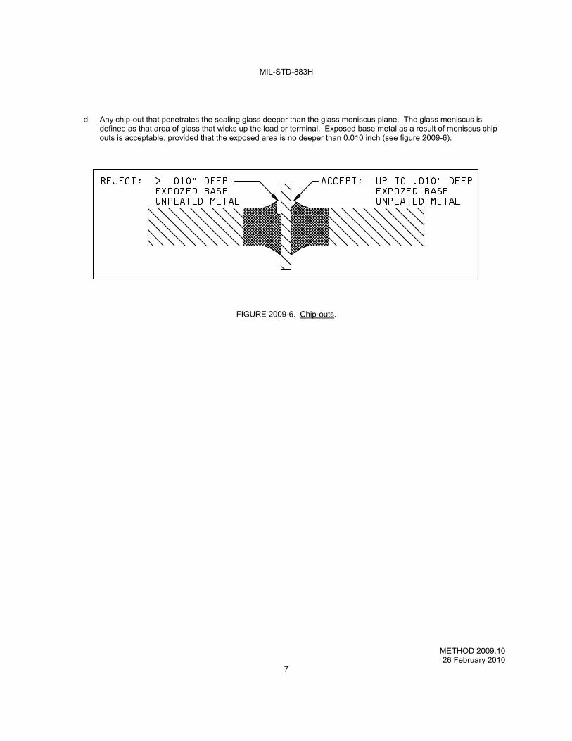
d. Any chip-out that penetrates the sealing glass deeper than the glass meniscus plane. The glass meniscus is defined as that area of glass that wicks up the lead or terminal. Exposed base metal as a result of meniscus chip outs is acceptable, provided that the exposed area is no deeper than 0.010 inch (see figure 2009-6).
FIGURE 2009-6. Chip-outs.
MIL-STD-883H
METHOD 2009.10 26 February 2010
8
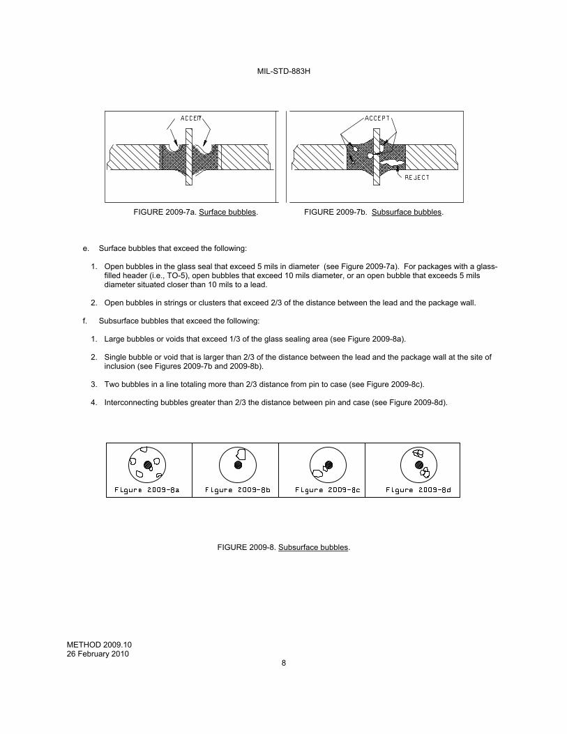
FIGURE 2009-7a. Surface bubbles. FIGURE 2009-7b. Subsurface bubbles.
e. Surface bubbles that exceed the following:
1. Open bubbles in the glass seal that exceed 5 mils in diameter (see Figure 2009-7a). For packages with a glass-filled header (i.e., TO-5), open bubbles that exceed 10 mils diameter, or an open bubble that exceeds 5 mils diameter situated closer than 10 mils to a lead.
2. Open bubbles in strings or clusters that exceed 2/3 of the distance between the lead and the package wall.
f. Subsurface bubbles that exceed the following:
1. Large bubbles or voids that exceed 1/3 of the glass sealing area (see Figure 2009-8a).
2. Single bubble or void that is larger than 2/3 of the distance between the lead and the package wall at the site of
inclusion (see Figures 2009-7b and 2009-8b).
3. Two bubbles in a line totaling more than 2/3 distance from pin to case (see Figure 2009-8c). 4. Interconnecting bubbles greater than 2/3 the distance between pin and case (see Figure 2009-8d).
FIGURE 2009-8. Subsurface bubbles.
MIL-STD-883H
METHOD 2009.10 26 February 2010
9
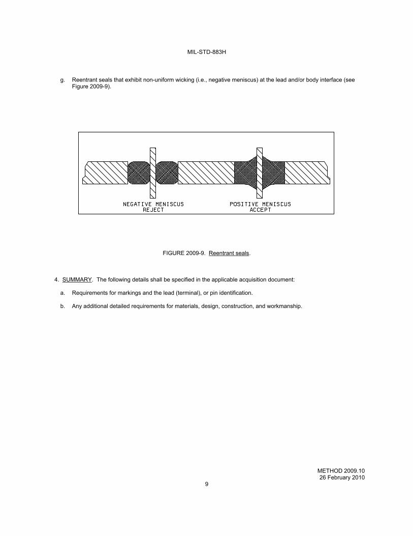
g. Reentrant seals that exhibit non-uniform wicking (i.e., negative meniscus) at the lead and/or body interface (see
Figure 2009-9).
FIGURE 2009-9. Reentrant seals.
4. SUMMARY. The following details shall be specified in the applicable acquisition document:
a. Requirements for markings and the lead (terminal), or pin identification.
b. Any additional detailed requirements for materials, design, construction, and workmanship.
MIL-STD-883H
METHOD 2009.10 26 February 2010
10
This page intentionally left blank
MIL-STD-883H
METHOD 2010.12 26 February 2010
1
METHOD 2010.12
INTERNAL VISUAL (MONOLITHIC) 1. PURPOSE. The purpose of this test is to check the internal materials, construction, and workmanship of microcircuits for compliance with the requirements of the applicable acquisition document. This test will normally be used prior to capping or encapsulation on a 100 percent inspection basis to detect and eliminate devices with internal defects, that could lead to device failure in normal applications. It may also be employed on a sampling basis prior to capping to determine the effectiveness of the manufacturer's quality control and handling procedures for microelectronic devices. Furthermore, the criteria of this test method will be used during destructive physical analysis (DPA) following the procedures outlined in test method 5009, "Destructive Physical Analysis". Test condition A and B provide a rigorous and detailed procedure for internal visual inspection of high reliability microcircuits as specified in the screening requirements of test method 5004. For condition B product the alternate screening procedure (alternate 1) documented in test method 5004 may be used by the manufacturer as an option to internal visual inspection as specified. For condition A or B product, the alternate screening procedure (alternate 2) documented in test method 5004 may be used by the manufacture as an option to internal visual inspection as specified.
2. APPARATUS. The apparatus for this test shall include optical equipment capable of the specified magnification and any visual standards (gauges, drawings, photographs, etc.) necessary to perform an effective examination and enable the operator to make objective decisions as to the acceptability of the device being examined. Adequate fixturing shall be provided for handling devices during examination to promote efficient operation without inflicting damage to the units.
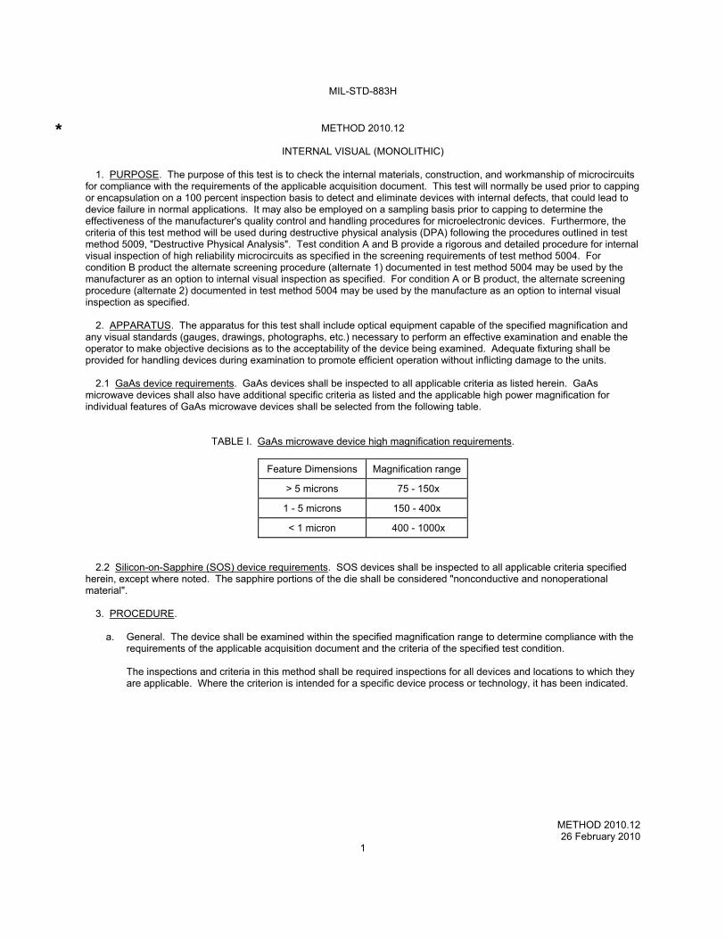
2.1 GaAs device requirements. GaAs devices shall be inspected to all applicable criteria as listed herein. GaAs microwave devices shall also have additional specific criteria as listed and the applicable high power magnification for individual features of GaAs microwave devices shall be selected from the following table.
TABLE I. GaAs microwave device high magnification requirements.
Feature Dimensions Magnification range
> 5 microns 75 - 150x
1 - 5 microns 150 - 400x
< 1 micron 400 - 1000x
2.2 Silicon-on-Sapphire (SOS) device requirements. SOS devices shall be inspected to all applicable criteria specified herein, except where noted. The sapphire portions of the die shall be considered "nonconductive and nonoperational material".
3. PROCEDURE.
a. General. The device shall be examined within the specified magnification range to determine compliance with the requirements of the applicable acquisition document and the criteria of the specified test condition.
The inspections and criteria in this method shall be required inspections for all devices and locations to which they
are applicable. Where the criterion is intended for a specific device process or technology, it has been indicated.
*
MIL-STD-883H
METHOD 2010.12 26 February 2010
2
b. Sequence of inspection. The order in which criteria are presented is not a required order of examination and may
be varied at the discretion of the manufacturer. When inverted die mounting techniques are employed, the inspection criteria contained herein that cannot be
performed after mounting shall be conducted prior to attachment of the die. Devices that fail any test criteria herein are defective devices and shall be rejected and removed at the time of observation.
Visual criteria may be inspected as follows:
(1) Prior to die attachment without re-examination after die attachment; 3.1.1.2, 3.1.1.5, 3.1.1.7, 3.1.2, 3.1.4 e
and f, 3.1.5, 3.1.6 a-f, 3.2.6. (2) Prior to bonding without re-examination after bonding; 3.2.3. (3) For condition B only; the following criteria may be inspected prior to die attachment at high power, plus low
power after die attachment, provided a high magnification sample to sample size number = 45 accept number C = 0 is performed at precap inspection; 3.1.1.1, 3.1.1.3, 3.1.1.4, 3.1.1.6, 3.1.3, 3.1.4 a-d and g-o, 3.1.6 g and h, 3.1.7. If the sample fails the entire lot shall be reinspected at high magnification for the failed criteria.
c. Inspection control. In all cases, examination prior to final preseal inspection shall be performed under the same
quality program that is required at the final preseal inspection station. Care shall be exercised after inspections in accordance with 3b, to insure that defects created during subsequent handling will be detected and rejected at final preseal inspection. During the time interval between visual inspection and preparation for sealing, devices shall be stored in a controlled environment. Devices examined to condition A shall be inspected and prepared for sealing in a 100 (0.5 μm or greater) particles/cubic foot controlled environment (class 5 of ISO 14644-1) and devices examined to condition B criteria shall be inspected and prepared for sealing in a 100,000 (0.5 μm or greater) particles/cubic foot controlled environment (class 8 of ISO 14644-1), (see A.4.8.1.1.7 of appendix A of MIL-PRF-38535), except that the maximum allowable relative humidity in either environment shall not exceed 65 percent. Devices shall be in covered containers when transferred from one controlled environment to another.
d. Magnification. "High magnification" inspection shall be performed perpendicular to the die surface with the device
under illumination perpendicular to the die surface. "Low magnification" inspection shall be performed with a metallurgical or stereomicroscope with the device under suitable illumination. Low magnification may be performed at an angle other than 90 to the die surface to facilitate the inspection. The inspection criteria of 3.2.1 may be examined at "high magnification" at the manufacturer's option.
e. Reinspection. When inspection for product acceptance is conducted subsequent to the manufacturer's
inspection, the additional inspection may be performed at any magnification specified by the applicable test condition, unless a specific magnification is required by the acquisition document. When suspected defects or deficiencies are noted, additional inspection may be performed at magnifications needed to evaluate or resolve the suspect items.
*
MIL-STD-883H
METHOD 2010.12 26 February 2010
3
f. Definitions: (1) Active circuit area. All areas enclosed by the perimeter of functional circuit elements, operating metallization
or any connected combinations thereof excluding beam leads. (2) Coupling (air) bridge. A raised layer of metallization used for interconnection that is isolated from the
surface of the element.
(3) Block resistor. A thin film resistor which for purposes of trimming is designed to be much wider than would be dictated by power density requirements and shall be identified in the approved manufacturer's precap visual implementation document.
(4) Contact Via. The Via where dielectric material is etched away in order to expose the Under Bump
Metalization (UBM) on the bond pads or solder bump attach pads. (5) Channel. An area lying between the drain and the source of FET structures.
(6) Controlled environment. Shall be 1,000 (0.5 m or greater) particles/cubic foot controlled environment (class 6 of ISO 14644-1), (see A.4.8.1.1.7 of appendix A of MIL-PRF-38535), except that the maximum allowable relative humidity shall not exceed 65 percent.
(7) Crazing. The presence of numerous minute cracks in the referenced material, (e.g., glassivation crazing). (8) Detritus. Fragments of original or laser modified resistor material remaining in the kerf. (9) Die Coat. A thin layer of soft polyimide coating applied to the surface of a semiconductor element that is
intended to produce stress relief resulting from encapsulation and to protect the circuit from surface scratches. (10) Dielectric isolation. Electrical isolation of one or more elements of a monolithic semiconductor integrated
circuit by surrounding the elements with an isolating barrier such as semiconductor oxide. (11) Dielectric layer or layers. Dielectric layer or layers deposited on the die surface to protect the redistribution
metalization, and to create the contact via for solder bump pad. (12) Diffusion tub. A volume (or region) formed in a semiconductor material by a diffusion process (n- or p- type)
and isolated from the surrounding semiconductor material by a n-p or p-n junction or by a dielectric material (dielectric isolation, coplanar process, SOS, SOI).
(13) Foreign material. Any material that is foreign to the microcircuit or package, or any nonforeign material that
is displaced from its original or intended position within the microcircuit package. (14) Functional circuit elements. Diodes, transistors, crossunders, capacitors, and resistors. (15) Gate oxide. The oxide or other dielectric that separates gate metallization (or other material used for the
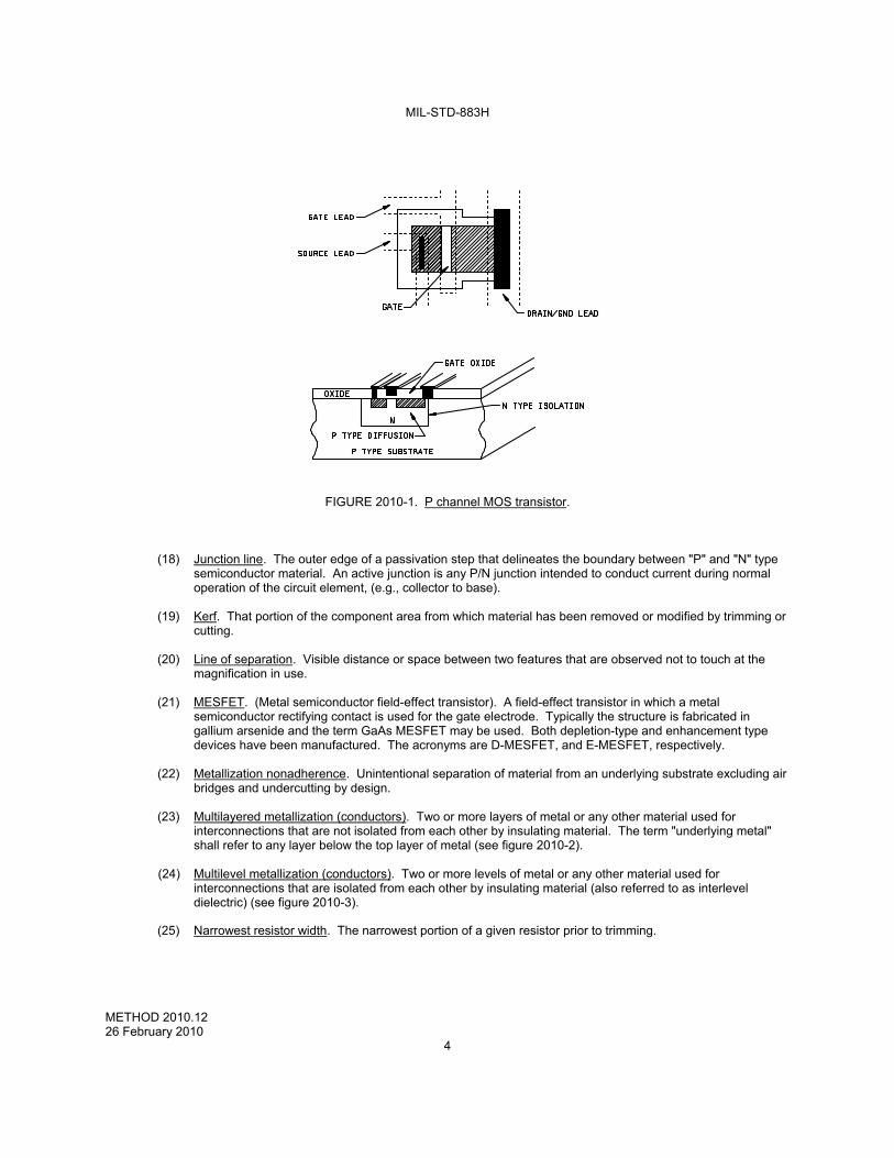
gate electrode) from the channel of MOS structures (see figure 2010-1).
(16) Glassivation. The top layer(s) of transparent insulating material that covers the active circuit area, with the exception of bonding pad areas and beam leads.
(17) Glassivation cracks. Fissures in the glassivation layer.
MIL-STD-883H
METHOD 2010.12 26 February 2010
4
FIGURE 2010-1. P channel MOS transistor. (18) Junction line. The outer edge of a passivation step that delineates the boundary between "P" and "N" type
semiconductor material. An active junction is any P/N junction intended to conduct current during normal operation of the circuit element, (e.g., collector to base).
(19) Kerf. That portion of the component area from which material has been removed or modified by trimming or
cutting. (20) Line of separation. Visible distance or space between two features that are observed not to touch at the
magnification in use. (21) MESFET. (Metal semiconductor field-effect transistor). A field-effect transistor in which a metal
semiconductor rectifying contact is used for the gate electrode. Typically the structure is fabricated in gallium arsenide and the term GaAs MESFET may be used. Both depletion-type and enhancement type devices have been manufactured. The acronyms are D-MESFET, and E-MESFET, respectively.
(22) Metallization nonadherence. Unintentional separation of material from an underlying substrate excluding air
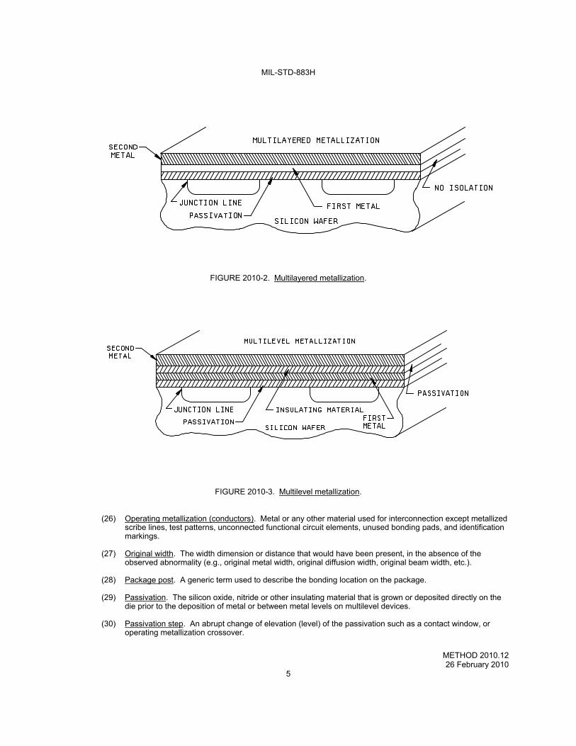
bridges and undercutting by design. (23) Multilayered metallization (conductors). Two or more layers of metal or any other material used for
interconnections that are not isolated from each other by insulating material. The term "underlying metal" shall refer to any layer below the top layer of metal (see figure 2010-2).
(24) Multilevel metallization (conductors). Two or more levels of metal or any other material used for
interconnections that are isolated from each other by insulating material (also referred to as interlevel dielectric) (see figure 2010-3).
(25) Narrowest resistor width. The narrowest portion of a given resistor prior to trimming.
MIL-STD-883H
METHOD 2010.12 26 February 2010
5
FIGURE 2010-2. Multilayered metallization.
FIGURE 2010-3. Multilevel metallization. (26) Operating metallization (conductors). Metal or any other material used for interconnection except metallized
scribe lines, test patterns, unconnected functional circuit elements, unused bonding pads, and identification markings.
(27) Original width. The width dimension or distance that would have been present, in the absence of the
observed abnormality (e.g., original metal width, original diffusion width, original beam width, etc.). (28) Package post. A generic term used to describe the bonding location on the package. (29) Passivation. The silicon oxide, nitride or other insulating material that is grown or deposited directly on the
die prior to the deposition of metal or between metal levels on multilevel devices. (30) Passivation step. An abrupt change of elevation (level) of the passivation such as a contact window, or
operating metallization crossover.
MIL-STD-883H
METHOD 2010.12 26 February 2010
6
(31) Peripheral metal. All metal that lies immediately adjacent to or over the scribe grid.
(32) Redistribution Layer (RDL). Layer added to original wafer/die surface to allow for the redistribution of bond pads into a format more suitable to flip chip.
(33) Redistribution metalization. The metal deposited on the RDL to create the electrical conductors which
connect the original bond pads to the distributed solder bump pads.
(34) Shooting metal. Metal (e.g., aluminum, gold) expulsion of various shapes and lengths from under the wire bond at the bonding pad.
(35) Solder ball. Solder ball or sphere attached to the UBM through the contact via after a re-flow process.
(36) Solder Bump. Solder that is either electroplated or screened into the photo resist opening. After the photo
resist is removed the solder resembles a bump before it is reflowed into ball or sphere.
(37) Substrate. The supporting structural material into or upon which or both the passivation, metallization and circuit elements are placed.
(38) Substrate via. A small hole formed through the wafer and metallized, causing electrical connection to be
made from the frontside (the side on which the circuitry is formed) to the backside of the wafer. (39) Thick film. That conductive/resistive/dielectric system that is a film having greater than 50,000Å thickness. (40) Thin film. That conductive/resistive/dielectric system that is a film equal to or less than 50,000Å in thickness. (41) Under Bump Metalization (UBM). Metals deposited on top of the aluminum bond pads or on the solder
bump pads that enhance wetting and protect against intermetalic reactions between the solder and the original metal on the pads.
(42) Via metallization. That which connects the metallization of one level to another.
g. Interpretations. Reference herein to "that exhibits" shall be considered satisfied when the visual image or visual
appearance of the device under examination indicates a specific condition is present and shall not require confirmation by any other method of testing. When other methods of test are to be used for confirming that a reject condition does not exist, they shall be approved by the acquiring activity. For inspections performed on the range of 75X to 100X, the criteria of 0.1 mil of passivation, separation or metal can be satisfied by a line of separation or a line of metal visible.
h. Foreign material control. The manufacturer shall perform an audit on a weekly basis for (1) the presence of
foreign material within incoming piece part lids and bases, and (2) the presence of foreign material on the die surface or within the package of assembled parts.
The audit of assembled parts may be satisfied during routine internal visual inspection. If the presence of foreign
material is discovered, the manufacturer shall perform the necessary analysis on a sample of the foreign material on the suspect devices to determine the nature of the material. The manufacturer shall document the results of this investigation and corrective action to eliminate the foreign material and this information will be available to the Government QAR, and the acquiring activity or the qualifying activity, as applicable. A corrective action plan shall be obtained within a maximum of 10 working days of discovery.
The audit of incoming piece part lids and bases shall be performed before parts are assembled, or may be
satisfied during routine incoming quality inspection. If the presence of foreign material of a size 1 mil or greater is discovered, the manufacturer will analyze the foreign material to determine its nature and document the results of the analysis. If applicable, these results shall be distributed to the vendor supplying the parts, with the request that the vendor document corrective actions to minimize or eliminate such foreign material. This information will be available to the manufacturer, Government QAR, and the acquiring activity or qualifying activity, as applicable.
MIL-STD-883H
METHOD 2010.12 26 February 2010
7
NOTE: The piece part audit requirements can be replaced by a piece part cleaning process, approved by the qualifying activity, that is always performed either prior to or during the assembly process and these piece parts are stored in a controlled environment until they are used.
The intent of these procedures is to require investigation and resolution of foreign material problems that do not
have an effective screening or detection methodology but that could cause degradation and eventual failure of the device function. Repetitive findings without obvious improvements require escalation to Director of Manufacturing and Director of Quality Assurance to continue processing.
Condition A Condition B Class level S Class level B
3.1 High power inspection. Internal visual examination as required in 3.1.1 through 3.1.3 shall be conducted on each microcircuit. In addition, the applicable criteria contained in 3.1.4 through 3.1.7 shall be used for the appropriate microcircuit area where glassivation, dielectric isolation or film resistors are used. NOTE: Unless otherwise specified, for flip chip product the criteria of 3.1 shall apply only to top circuit side inspection. After
die mounting, only criteria in 3.1.3i shall apply.
The high magnification The high magnification inspection shall be within the inspection shall be within the range of 100X to 200X. range of 75X to 150X.
For high magnification inspection of GaAs microwave devices, see table I herein. Also, for < 1 micron features, the manufacturer may implement a sample inspection plan which shall be documented in the manufacturer's internal procedure and approved by the qualifying activity.
3.1.1 Metallization defects. No device shall be acceptable that exhibits the following defects in the operating metallization.
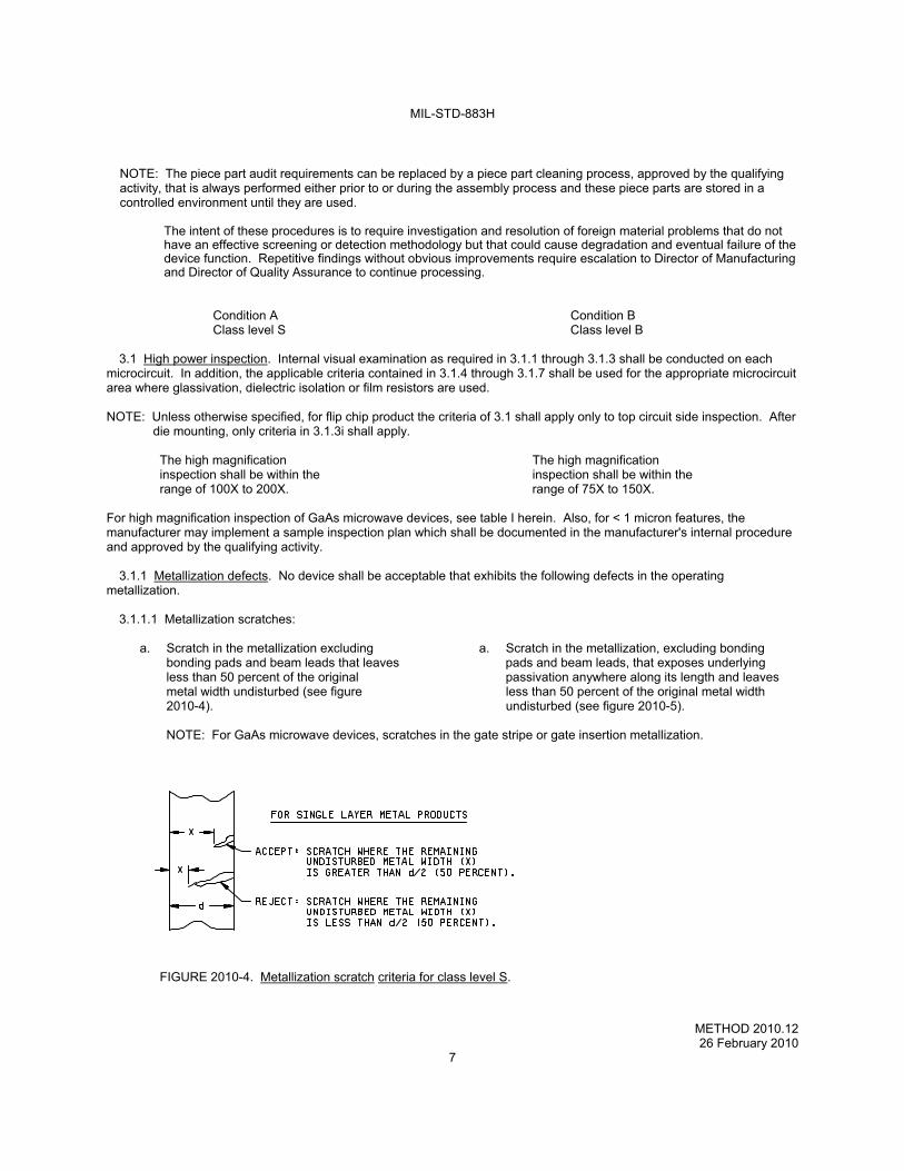
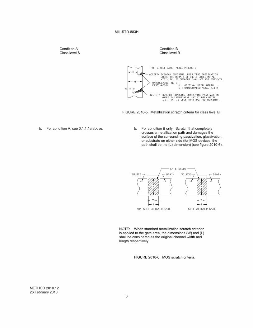
3.1.1.1 Metallization scratches:
a. Scratch in the metallization excluding a. Scratch in the metallization, excluding bonding bonding pads and beam leads that leaves pads and beam leads, that exposes underlying less than 50 percent of the original passivation anywhere along its length and leaves metal width undisturbed (see figure less than 50 percent of the original metal width 2010-4). undisturbed (see figure 2010-5).
NOTE: For GaAs microwave devices, scratches in the gate stripe or gate insertion metallization.
FIGURE 2010-4. Metallization scratch criteria for class level S.
MIL-STD-883H
METHOD 2010.12 26 February 2010
8
Condition A Condition B
Class level S Class level B
FIGURE 2010-5. Metallization scratch criteria for class level B.
b. For condition A, see 3.1.1.1a above. b. For condition B only. Scratch that completely
crosses a metallization path and damages the surface of the surrounding passivation, glassivation, or substrate on either side (for MOS devices, the path shall be the (L) dimension) (see figure 2010-6).
NOTE: When standard metallization scratch criterion is applied to the gate area, the dimensions (W) and (L)
shall be considered as the original channel width and length respectively.
FIGURE 2010-6. MOS scratch criteria.
MIL-STD-883H
METHOD 2010.12 26 February 2010
9
Condition A Condition B
Class level S Class level B
FIGURE 2010-6. MOS scratch criteria - Continued.
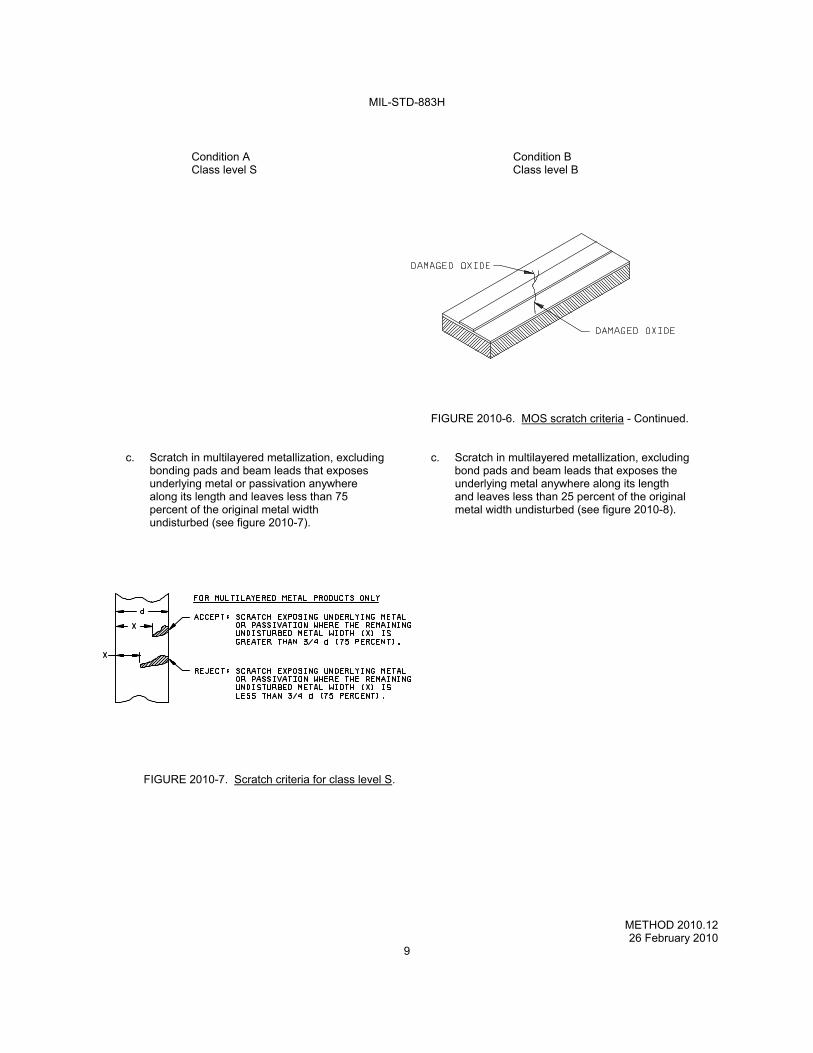
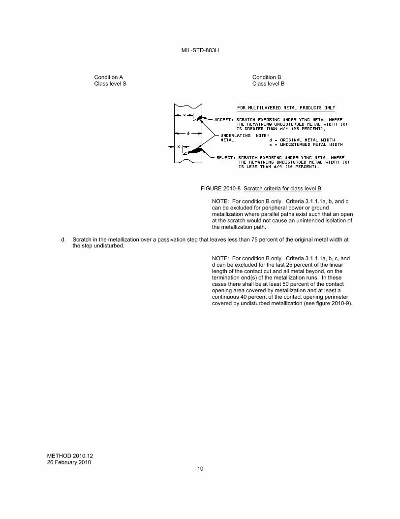
c. Scratch in multilayered metallization, excluding c. Scratch in multilayered metallization, excluding bonding pads and beam leads that exposes bond pads and beam leads that exposes the underlying metal or passivation anywhere underlying metal anywhere along its length along its length and leaves less than 75 and leaves less than 25 percent of the original percent of the original metal width metal width undisturbed (see figure 2010-8). undisturbed (see figure 2010-7).
FIGURE 2010-7. Scratch criteria for class level S.
MIL-STD-883H
METHOD 2010.12 26 February 2010
10
Condition A Condition B
Class level S Class level B
FIGURE 2010-8 Scratch criteria for class level B.
NOTE: For condition B only. Criteria 3.1.1.1a, b, and c can be excluded for peripheral power or ground metallization where parallel paths exist such that an open at the scratch would not cause an unintended isolation of the metallization path.
d. Scratch in the metallization over a passivation step that leaves less than 75 percent of the original metal width at
the step undisturbed.
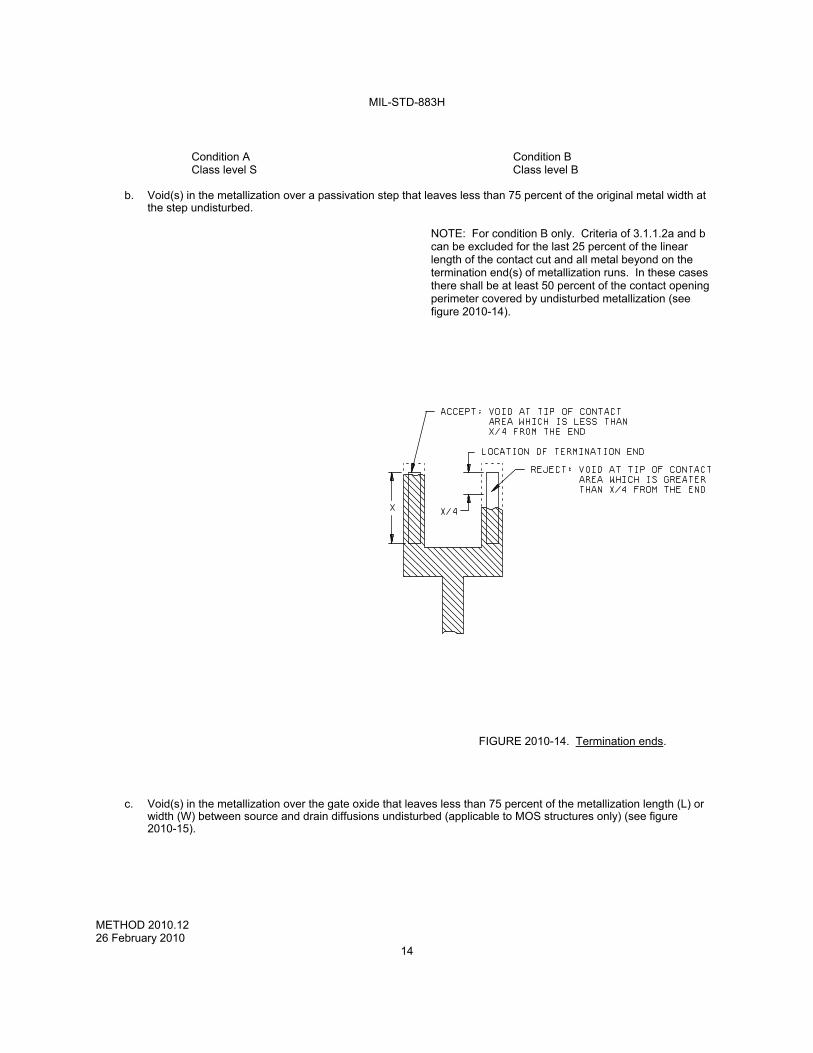
NOTE: For condition B only. Criteria 3.1.1.1a, b, c, and d can be excluded for the last 25 percent of the linear length of the contact cut and all metal beyond, on the termination end(s) of the metallization runs. In these cases there shall be at least 50 percent of the contact opening area covered by metallization and at least a continuous 40 percent of the contact opening perimeter covered by undisturbed metallization (see figure 2010-9).

MIL-STD-883H
METHOD 2010.12 26 February 2010
11
Condition A Condition B Class level S Class level B
FIGURE 2010-9. Termination ends.
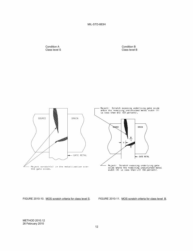
e. Scratch in the metallization, over the e. Scratch in the metallization, over the gate oxide (applicable to MOS structures gate oxide, that exposes underlying only) (see figure 2010-10). passivation and leaves less than 50 percent
of the length or width of the metallization between source and drain diffusion undisturbed (applicable to MOS structures only) (see figure
2010-11).
MIL-STD-883H
METHOD 2010.12 26 February 2010
12
Condition A Condition B Class level S Class level B
FIGURE 2010-10. MOS scratch criteria for class level S. FIGURE 2010-11. MOS scratch criteria for class level B.
MIL-STD-883H
METHOD 2010.12 26 February 2010
13
Condition A Condition B
Class level S Class level B
f. Scratch in the metallization that exposes the dielectric material of a thin film capacitor or crossover. (Not applicable to air bridges.)
g. Scratch in the bonding pad or fillet area that g. Scratch in the bonding pad or fillet area that reduces the metallization path width connecting exposes underlying passivation or substrate the bond to the interconnecting metallization and reduces the metallization path width to less than 50 percent of the narrowest connecting the bond to the interconnecting entering interconnect metallization stripe metallization to less than 50 percent of the width. If two or more stripes enter a bonding narrowest entering interconnect metallization pad, each shall be considered separately. stripe width. If two or more stripes enter a bonding pad, each shall be considered
separately.
h. Scratch(es) (probe mark(s), etc.) in the bonding pad area that exposes underlying passivation or substrate and leaves less than 75 percent of the unglassivated metallization area undisturbed.
i. For GaAs devices only, any tears, peeling, gaps, and lateral displacement of metal.
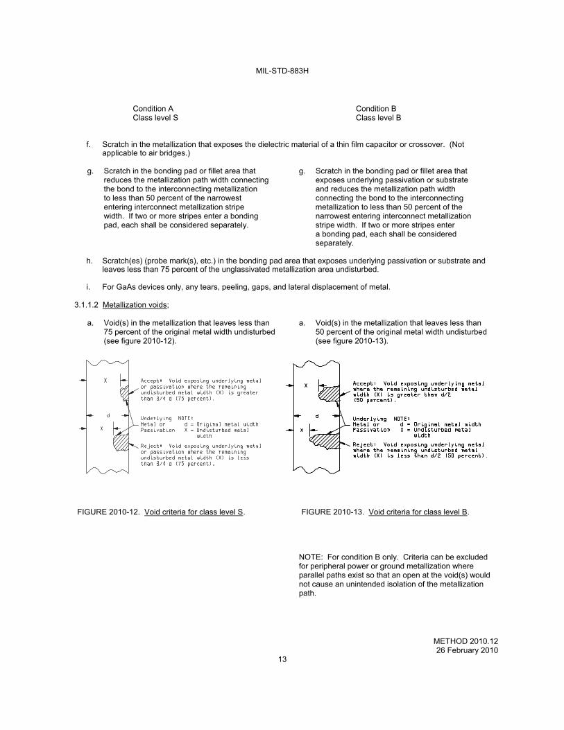
3.1.1.2 Metallization voids;
a. Void(s) in the metallization that leaves less than a. Void(s) in the metallization that leaves less than 75 percent of the original metal width undisturbed 50 percent of the original metal width undisturbed (see figure 2010-12). (see figure 2010-13).
FIGURE 2010-12. Void criteria for class level S. FIGURE 2010-13. Void criteria for class level B.
NOTE: For condition B only. Criteria can be excluded for peripheral power or ground metallization where parallel paths exist so that an open at the void(s) would not cause an unintended isolation of the metallization path.
MIL-STD-883H
METHOD 2010.12 26 February 2010
14
Condition A Condition B
Class level S Class level B
b. Void(s) in the metallization over a passivation step that leaves less than 75 percent of the original metal width at the step undisturbed.
NOTE: For condition B only. Criteria of 3.1.1.2a and b can be excluded for the last 25 percent of the linear length of the contact cut and all metal beyond on the termination end(s) of metallization runs. In these cases there shall be at least 50 percent of the contact opening perimeter covered by undisturbed metallization (see figure 2010-14).
FIGURE 2010-14. Termination ends.
c. Void(s) in the metallization over the gate oxide that leaves less than 75 percent of the metallization length (L) or
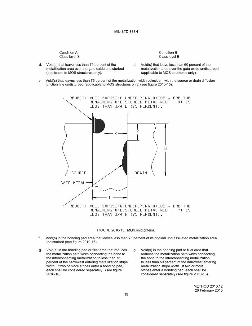
width (W) between source and drain diffusions undisturbed (applicable to MOS structures only) (see figure 2010-15).
MIL-STD-883H
METHOD 2010.12 26 February 2010
15
Condition A Condition B Class level S Class level B
d. Void(s) that leave less than 75 percent of the d. Void(s) that leave less than 60 percent of the metallization area over the gate oxide undisturbed metallization area over the gate oxide undisturbed (applicable to MOS structures only). (applicable to MOS structures only).
e. Void(s) that leaves less than 75 percent of the metallization width coincident with the source or drain diffusion
junction line undisturbed (applicable to MOS structures only) (see figure 2010-15).
FIGURE 2010-15. MOS void criteria.
f. Void(s) in the bonding pad area that leaves less than 75 percent of its original unglassivated metallization area undisturbed (see figure 2010-16).
g. Void(s) in the bonding pad or fillet area that reduces g. Void(s) in the bonding pad or fillet area that the metallization path width connecting the bond to reduces the metallization path width connecting the interconnecting metallization to less than 75 the bond to the interconnecting metallization percent of the narrowest entering metallization stripe to less than 50 percent of the narrowest entering width. If two or more stripes enter a bonding pad, metallization stripe width. If two or more each shall be considered separately. (see figure stripes enter a bonding pad, each shall be 2010-16). considered separately (see figure 2010-16).
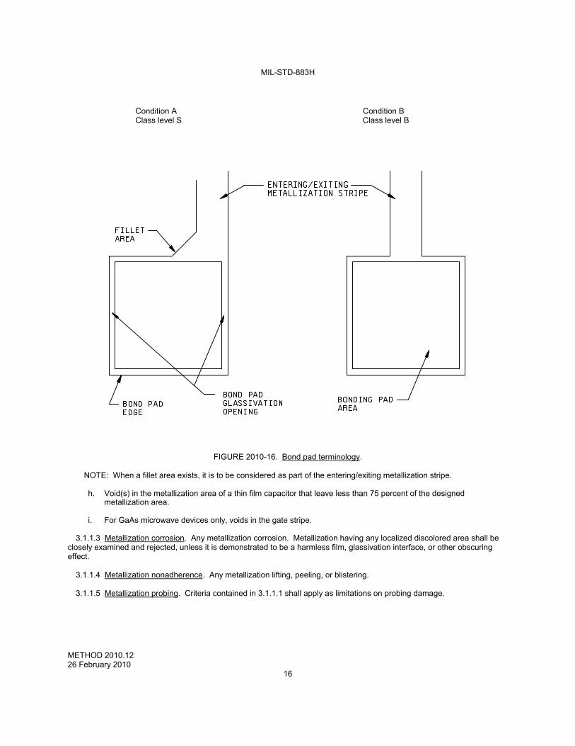
MIL-STD-883H
METHOD 2010.12 26 February 2010
16
Condition A Condition B
Class level S Class level B
FIGURE 2010-16. Bond pad terminology.
NOTE: When a fillet area exists, it is to be considered as part of the entering/exiting metallization stripe.
h. Void(s) in the metallization area of a thin film capacitor that leave less than 75 percent of the designed metallization area.
i. For GaAs microwave devices only, voids in the gate stripe.
3.1.1.3 Metallization corrosion. Any metallization corrosion. Metallization having any localized discolored area shall be closely examined and rejected, unless it is demonstrated to be a harmless film, glassivation interface, or other obscuring effect.
3.1.1.4 Metallization nonadherence. Any metallization lifting, peeling, or blistering.
3.1.1.5 Metallization probing. Criteria contained in 3.1.1.1 shall apply as limitations on probing damage.
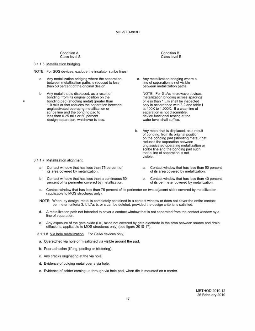
MIL-STD-883H
METHOD 2010.12 26 February 2010
17
Condition A Condition B Class level S Class level B
3.1.1.6 Metallization bridging.
NOTE: For SOS devices, exclude the insulator scribe lines.
a. Any metallization bridging where the separation a. Any metallization bridging where a between metallization paths is reduced to less line of separation is not visible than 50 percent of the original design. between metallization paths. b. Any metal that is displaced, as a result of NOTE: For GaAs microwave devices, bonding, from its original position on the metallization bridging across spacings bonding pad (shooting metal) greater than of less than 1 m shall be inspected 1.0 mils or that reduces the separation between only in accordance with 3.2 and table I unglassivated operating metallization or at 400X to 1,000X. If a clear line of scribe line and the bonding pad to separation is not discernible, less than 0.25 mils or 50 percent device functional testing at the design separation, whichever is less. wafer level shall suffice.
b. Any metal that is displaced, as a result
of bonding, from its original position on the bonding pad (shooting metal) that reduces the separation between unglassivated operating metallization or scribe line and the bonding pad such that a line of separation is not visible.
3.1.1.7 Metallization alignment.
a. Contact window that has less than 75 percent of a. Contact window that has less than 50 percent its area covered by metallization. of its area covered by metallization.
b. Contact window that has less than a continuous 50 b. Contact window that has less than 40 percent percent of its perimeter covered by metallization. of its perimeter covered by metallization.
c. Contact window that has less than 75 percent of its perimeter on two adjacent sides covered by metallization
(applicable to MOS structures only).
NOTE: When, by design, metal is completely contained in a contact window or does not cover the entire contact perimeter, criteria 3.1.1.7a, b, or c can be deleted, provided the design criteria is satisfied.
d. A metallization path not intended to cover a contact window that is not separated from the contact window by a
line of separation.
e. Any exposure of the gate oxide (i.e., oxide not covered by gate electrode in the area between source and drain diffusions, applicable to MOS structures only) (see figure 2010-17).
3.1.1.8 Via hole metallization. For GaAs devices only,
a. Overetched via hole or misaligned via visible around the pad.
b. Poor adhesion (lifting, peeling or blistering).
c. Any cracks originating at the via hole.
d. Evidence of bulging metal over a via hole.
e. Evidence of solder coming up through via hole pad, when die is mounted on a carrier.
*
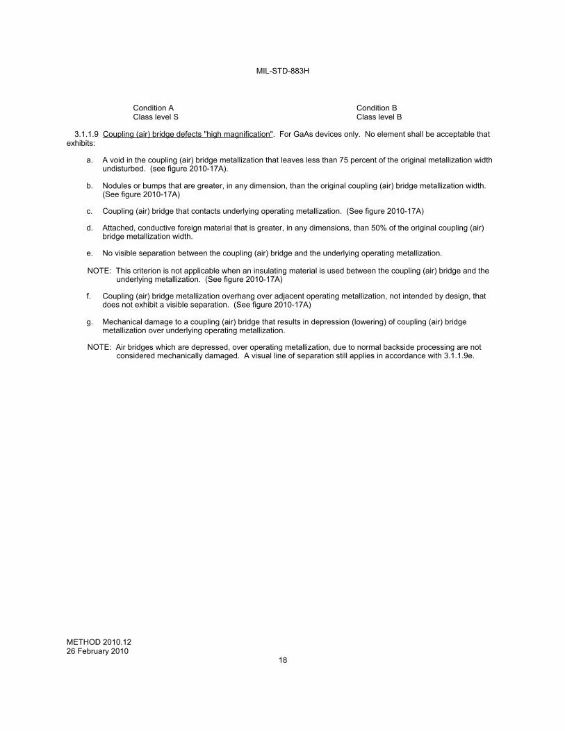
MIL-STD-883H
METHOD 2010.12 26 February 2010
18
Condition A Condition B
Class level S Class level B
3.1.1.9 Coupling (air) bridge defects "high magnification". For GaAs devices only. No element shall be acceptable that exhibits:
a. A void in the coupling (air) bridge metallization that leaves less than 75 percent of the original metallization width undisturbed. (see figure 2010-17A).
b. Nodules or bumps that are greater, in any dimension, than the original coupling (air) bridge metallization width.
(See figure 2010-17A)
c. Coupling (air) bridge that contacts underlying operating metallization. (See figure 2010-17A)
d. Attached, conductive foreign material that is greater, in any dimensions, than 50% of the original coupling (air) bridge metallization width.
e. No visible separation between the coupling (air) bridge and the underlying operating metallization.
NOTE: This criterion is not applicable when an insulating material is used between the coupling (air) bridge and the
underlying metallization. (See figure 2010-17A)
f. Coupling (air) bridge metallization overhang over adjacent operating metallization, not intended by design, that does not exhibit a visible separation. (See figure 2010-17A)
g. Mechanical damage to a coupling (air) bridge that results in depression (lowering) of coupling (air) bridge
metallization over underlying operating metallization.
NOTE: Air bridges which are depressed, over operating metallization, due to normal backside processing are not considered mechanically damaged. A visual line of separation still applies in accordance with 3.1.1.9e.

MIL-STD-883H
METHOD 2010.12 26 February 2010
19
FIGURE 2010-17A. Class level S and Class level B coupling (air) bridge criteria.
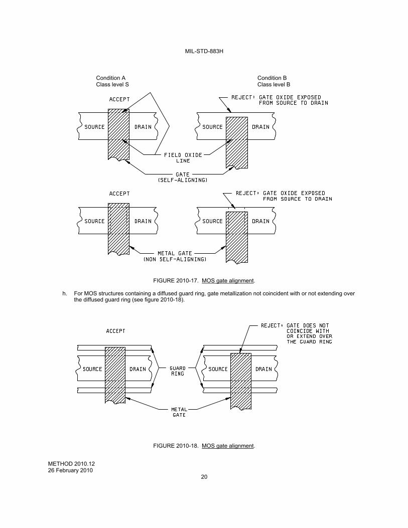
MIL-STD-883H
METHOD 2010.12 26 February 2010
20
Condition A Condition B
Class level S Class level B
FIGURE 2010-17. MOS gate alignment.
h. For MOS structures containing a diffused guard ring, gate metallization not coincident with or not extending over
the diffused guard ring (see figure 2010-18).
FIGURE 2010-18. MOS gate alignment.
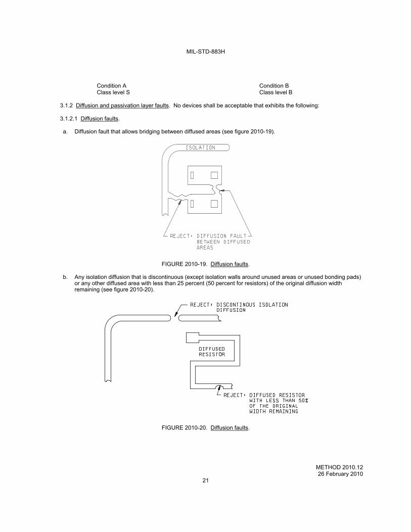
MIL-STD-883H
METHOD 2010.12 26 February 2010
21
Condition A Condition B Class level S Class level B
3.1.2 Diffusion and passivation layer faults. No devices shall be acceptable that exhibits the following:
3.1.2.1 Diffusion faults.
a. Diffusion fault that allows bridging between diffused areas (see figure 2010-19).
FIGURE 2010-19. Diffusion faults.
b. Any isolation diffusion that is discontinuous (except isolation walls around unused areas or unused bonding pads) or any other diffused area with less than 25 percent (50 percent for resistors) of the original diffusion width remaining (see figure 2010-20).
FIGURE 2010-20. Diffusion faults.
MIL-STD-883H
METHOD 2010.12 26 February 2010
22
Condition A Condition B
Class level S Class level B 3.1.2.2 Passivation faults.
NOTE: For SOS devices, exclude defects between first-level conductive interconnect (metallization, polysilicon, ect.) and
sapphire areas of the die, where no active circuit elements are present.
a. Either multiple lines or a complete absence of passivation visible at the edge and continuing under the metallization unless by design for GaAs devices. Multiple lines indicate that the fault can have sufficient depth to penetrate down to bare semiconductor material.
NOTE: The multiple line criteria can be excluded when a second passivation layer is applied in a separate operation
prior to metallization deposition or for bond pads located in isolated tubs.
NOTE: For condition B only. Should the absence of glassivation in the defect area or the characteristics of the glassivation present allow verification of the presence or absence of passivation by color or color comparisons respectively, then these techniques may be used (see figure 2010-21).
FIGURE 2010-21. Passivation faults.
b. Active junction line not covered by passivation, unless by design.
c. Contact window that extends across a junction line, unless by design.
MIL-STD-883H
METHOD 2010.12 26 February 2010
23
Condition A Condition B
Class level S Class level B 3.1.3 Scribing and die defects. No device shall be acceptable that exhibits:
a. Less than 0.25 mil of passivation visible a. No line of separation between operating between operating metallization or bond metallization or bond periphery and bare periphery and bare semiconductor material semiconductor material (see figure 2010-22). (see figure 2010-22).
NOTE: For GaAs devices only, less than 0.1 mil of substrate visible between operating metallization or bond periphery
and edge of the die.
NOTE: Criteria can be excluded for beam leads and peripheral metallization including bonding pads where the metallization is at the same potential as the substrate.
NOTE: Does not apply to SOS devices.
b. A chipout or crack in the active circuit area (see figures 2010-22 and 2010-38). In addition for GaAs a chipout into
or underneath the functional metallization, e.g., bond pads, capacitors, peripheral metallization, etc., but excluding test structures of the device.
NOTE: Criteria can be excluded for peripheral metallization that is at the same potential as the substrate. At least 50
percent undisturbed metallization width shall remain at the chipout.
c. A crack that exceeds 3.0 mils in length, or c. A crack that exceed 5.0 mils in length, or comes closer than 0.25 mils to any operating that does not exhibit a line of separation to metallization (except for substrate potential any operating metallization (except for peripheral metal) or functional circuit element substrate potential peripheral metal) or (see figure 2010-22). function circuit element (see figure 2010-22).
d. For condition A only. Semicircular crack(s) d. No condition B. terminating at the die edge, whose chord is long enough to bridge the narrowest spacing between unglassivated operating material (e.g., metallization, bare semiconductor material, mounting material, bonding wire, etc.) (see figure 2010-22). .
e. Exposed semiconductor material extending over the passivation edge at the point of the beam lead exit from the die (applicable to beam lead structures only) (see figure 2010-38).
f. Die having attached portions of the active circuit area of another die.
g. A crack that exceeds 1.0 mil in length inside the scribe line (or semiconductor material edge for beam lead
devices) that points toward operating metallization or functional circuit elements (see figure 2010-22).
h. A crack that comes closer than 0.5 mil to operating beam lead metallization (see figure 2010-38).
NOTE: Criteria of 3.1.3c and h can be excluded for beam lead devices where the chipout or crack does not extend into the semiconductor material.
NOTE: Criteria of 3.1.3e and h do not apply to GaAs devices.
MIL-STD-883H
METHOD 2010.12 26 February 2010
24
FIGURE 2010-22 Scribing and die defects.
MIL-STD-883H
METHOD 2010.12 26 February 2010
25
Condition A Condition B
Class level S Class level B
i. For flip chip, cracks, or chipouts in the substrate material that extends beyond 50 percent of substrate thickness or a crack greater than 5.0 mils in length in the substrate material (see figure 2010-23).
FIGURE 2010-23. Scribing and die defects.
j. Any blistering, peeling, delamination, corrosion, or other gross defects in glassivation, metal, interlevel dielectrics or other layers.
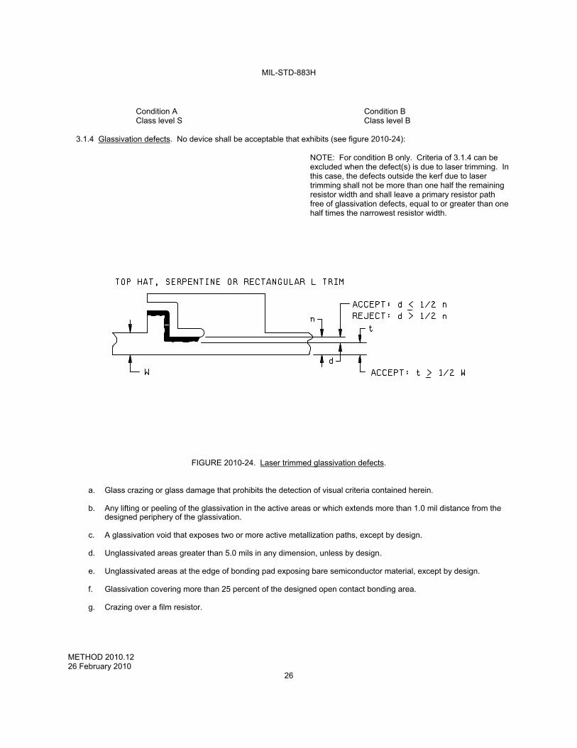
MIL-STD-883H
METHOD 2010.12 26 February 2010
26
Condition A Condition B
Class level S Class level B 3.1.4 Glassivation defects. No device shall be acceptable that exhibits (see figure 2010-24):
NOTE: For condition B only. Criteria of 3.1.4 can be excluded when the defect(s) is due to laser trimming. In this case, the defects outside the kerf due to laser trimming shall not be more than one half the remaining resistor width and shall leave a primary resistor path free of glassivation defects, equal to or greater than one half times the narrowest resistor width.
FIGURE 2010-24. Laser trimmed glassivation defects.
a. Glass crazing or glass damage that prohibits the detection of visual criteria contained herein.
b. Any lifting or peeling of the glassivation in the active areas or which extends more than 1.0 mil distance from the designed periphery of the glassivation.
c. A glassivation void that exposes two or more active metallization paths, except by design.
d. Unglassivated areas greater than 5.0 mils in any dimension, unless by design.
e. Unglassivated areas at the edge of bonding pad exposing bare semiconductor material, except by design.
f. Glassivation covering more than 25 percent of the designed open contact bonding area.
g. Crazing over a film resistor.
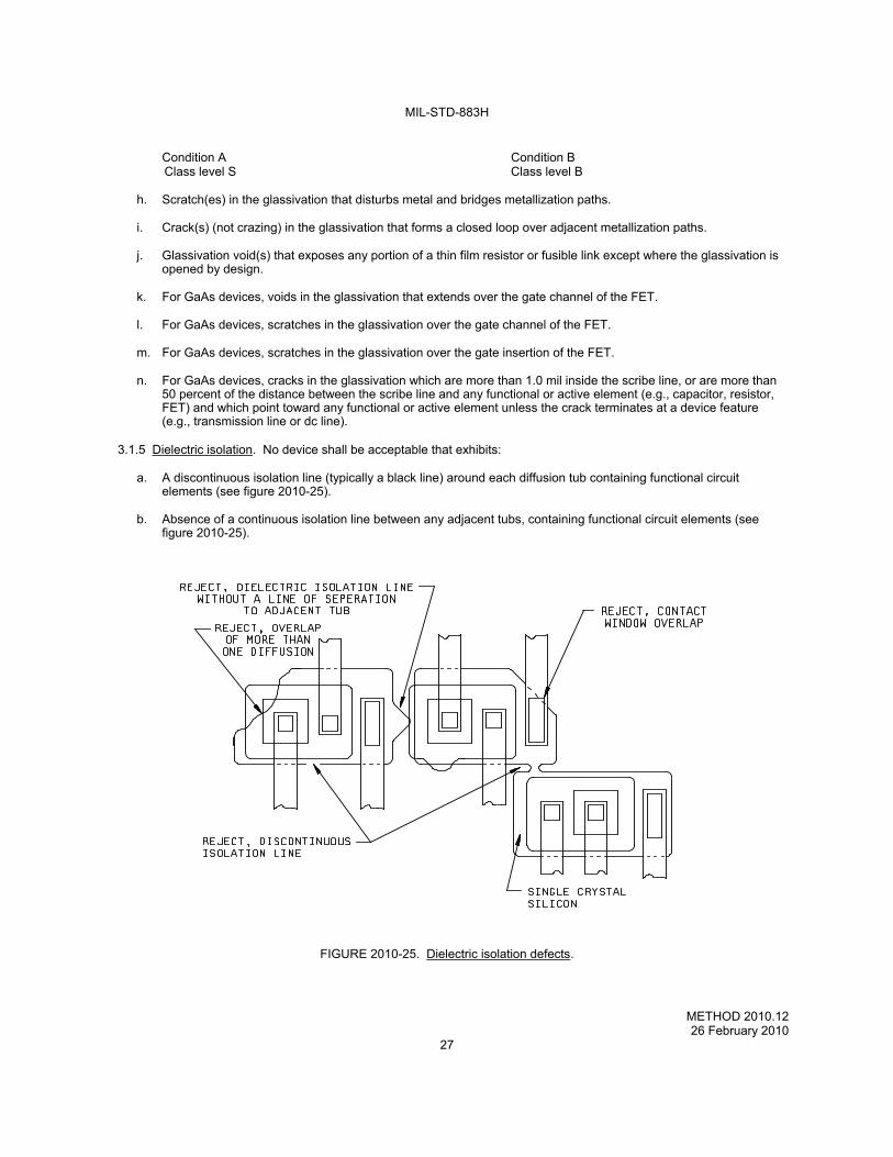
MIL-STD-883H
METHOD 2010.12 26 February 2010
27
Condition A Condition B Class level S Class level B
h. Scratch(es) in the glassivation that disturbs metal and bridges metallization paths.
i. Crack(s) (not crazing) in the glassivation that forms a closed loop over adjacent metallization paths.
j. Glassivation void(s) that exposes any portion of a thin film resistor or fusible link except where the glassivation is
opened by design.
k. For GaAs devices, voids in the glassivation that extends over the gate channel of the FET.
l. For GaAs devices, scratches in the glassivation over the gate channel of the FET.
m. For GaAs devices, scratches in the glassivation over the gate insertion of the FET.
n. For GaAs devices, cracks in the glassivation which are more than 1.0 mil inside the scribe line, or are more than 50 percent of the distance between the scribe line and any functional or active element (e.g., capacitor, resistor, FET) and which point toward any functional or active element unless the crack terminates at a device feature (e.g., transmission line or dc line).
3.1.5 Dielectric isolation. No device shall be acceptable that exhibits:
a. A discontinuous isolation line (typically a black line) around each diffusion tub containing functional circuit
elements (see figure 2010-25).
b. Absence of a continuous isolation line between any adjacent tubs, containing functional circuit elements (see figure 2010-25).
FIGURE 2010-25. Dielectric isolation defects.

MIL-STD-883H
METHOD 2010.12 26 February 2010
28
Condition A Condition B Class level S Class level B
c. A diffused area which overlaps dielectric isolation material and does not exhibit a line of separation to an adjacent
tub, or an overlap of more than one diffusion area into the dielectric isolation material (see figure 2010-25).
FIGURE 2010-26. Dielectric isolation defects.
d. A contact window that touches or overlaps dielectric material, except by design.
NOTE: Metallization scratch and void defects over a dielectric isolation step shall be rejected in accordance with criteria contained in 3.1.1.1d and 3.1.1.2b.
3.1.6 Film resistor. Rejection shall be based on defects found within the actively used portions of the film resistor.
Metallization defect criteria of 3.1.1 shall apply as applicable. No device shall be acceptable that exhibits:
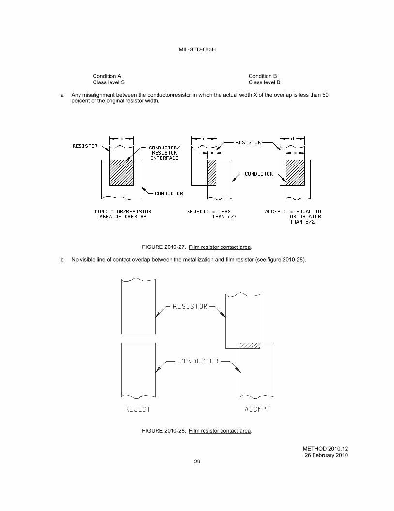
MIL-STD-883H
METHOD 2010.12 26 February 2010
29
Condition A Condition B
Class level S Class level B
a. Any misalignment between the conductor/resistor in which the actual width X of the overlap is less than 50 percent of the original resistor width.
FIGURE 2010-27. Film resistor contact area.
b. No visible line of contact overlap between the metallization and film resistor (see figure 2010-28).
FIGURE 2010-28. Film resistor contact area.
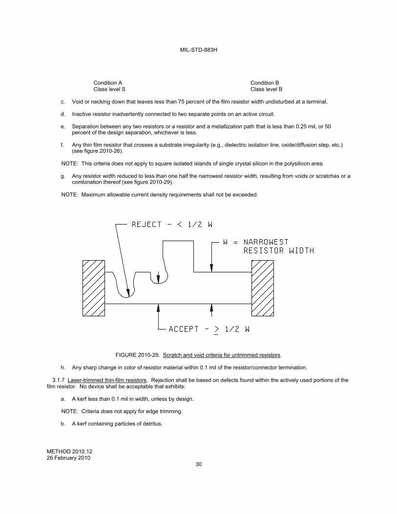
MIL-STD-883H
METHOD 2010.12 26 February 2010
30
Condition A Condition B Class level S Class level B
c. Void or necking down that leaves less than 75 percent of the film resistor width undisturbed at a terminal.
d. Inactive resistor inadvertently connected to two separate points on an active circuit.
e. Separation between any two resistors or a resistor and a metallization path that is less than 0.25 mil, or 50
percent of the design separation, whichever is less.
f. Any thin film resistor that crosses a substrate irregularity (e.g., dielectric isolation line, oxide/diffusion step, etc.) (see figure 2010-26).
NOTE: This criteria does not apply to square isolated islands of single crystal silicon in the polysilicon area.
g. Any resistor width reduced to less than one half the narrowest resistor width, resulting from voids or scratches or a
combination thereof (see figure 2010-29).
NOTE: Maximum allowable current density requirements shall not be exceeded.
FIGURE 2010-29. Scratch and void criteria for untrimmed resistors.
h. Any sharp change in color of resistor material within 0.1 mil of the resistor/connector termination. 3.1.7 Laser-trimmed thin-film resistors. Rejection shall be based on defects found within the actively used portions of the
film resistor. No device shall be acceptable that exhibits:
a. A kerf less than 0.1 mil in width, unless by design.
NOTE: Criteria does not apply for edge trimming.
b. A kerf containing particles of detritus.
MIL-STD-883H
METHOD 2010.12 26 February 2010
31
Condition A Condition B
Class level S Class level B
c. A kerf containing untrimmed resistor material, unless that material is continuous across the kerf, and is undisturbed for a width greater than one-half times the narrowest resistor width, unless by design (see figure 2010-30).
NOTE: Maximum allowable current density requirements shall not be exceeded.
Top hat trim
FIGURE 2010-30. Resistor Criteria.
MIL-STD-883H
METHOD 2010.12 26 February 2010
32
Condition A Condition B Class level S Class level B
Rectangular L trim
FIGURE 2010-30. Resistor Criteria - Continued.
d. Resistor width that has been reduced by trimming to less than one-half the narrowest resistor width, including voids, scratches, or a combination thereof, in the trim area (see figure 2010-31).
NOTE: Trimming of more than 50 percent of a given resistor shunt link is acceptable by design providing that the last
shunt link of the resistor adder network is not trimmed greater than 50 percent. All trimmable resistor shunt links shall be defined on the design layout drawing.
MIL-STD-883H
METHOD 2010.12 26 February 2010
33
FIGURE 2010-31. Scratch, void and trim criteria for resistors.
MIL-STD-883H
METHOD 2010.12 26 February 2010
34
Condition A Condition B
Class level S Class level B
e. Trim path into the metallization except block resistors.
NOTE: This criteria can be excluded for trim paths into terminator ends of metallization runs. Conductors or resistors may be trimmed open for link trims or by design.
f. Trim for block resistors which extends into the metallization (excluding bonding pads) more than 25 percent of the
original metal width (see figure 2010-32).
FIGURE 2010-32. Block resistor criteria.
g. Pits into the silicon dioxide in the kerf which do not exhibit a line of separation between the pit and the resistor material.

MIL-STD-883H
METHOD 2010.12 26 February 2010
35
Condition A Condition B
Class level S Class level B 3.2 Low power inspection. Internal visual examination as required in 3.2.1 through 3.2.3 shall be conducted on each
microcircuit at low magnification range of 30X to 60X. In addition, the applicable criteria contained in 3.2.4 shall be applicable where beam lead assembly technology is used and 3.2.5 shall be inspected at both high and low power as indicated, high power magnification shall be same as 3.1, subject to conditions in 3b.
3.2.1 Lower power wire bond inspection. This inspection and criteria shall be required inspection for the bond type (s) and location(s) to which they are applicable when viewed from above (see figure 2010-33). NOTE: The criteria applicable for bonds (called "wedgebonds" or "bonds") in this test method refers to the fully or partially
deformed area including the tool impression shown as "L and W" in figure. The criteria applicable for "bond tails" (or "tails") in this test method refers to resulting length of bonding wire extending beyond the bond shown as "T" in figure 2010-33. Tail is not part of bond.
FIGURE 2010-33. Bond dimensions.
MIL-STD-883H
METHOD 2010.12 26 February 2010
36
Condition A Condition B
Class level S Class level B 3.2.1.1 Gold ball bonds. No devices shall be acceptable that exhibits:
a. Gold ball bonds on the die or package post wherein the ball bond diameter is less than 2.0 times or greater than
5.0 times the wire diameter.
b. Gold ball bonds where the wire exit is not completely within the periphery of the ball.
c. Gold ball bonds where the wire center exit is not within the boundaries of the unglassivated bonding pad area.
3.2.1.2 Wedge bonds. No device shall be acceptable that exhibits:
a. Ultrasonic wedge bonds on the die or package post that are less than 1.2 times or more than 3.0 times the wire diameter in width, or less than 1.5 times or more than 6.0 times the wire diameter in length.
b. Thermosonic wedge bonds on the die or package post that are less than 1.5 times or more than 3.0 times the wire
diameter in width or are less than 1.5 times or more than 6.0 times the wire diameter in length.
c. Bond width less than 1.0 times the wire diameter for aluminum wires 2.0 mils or greater in diameter.
d. Wedge bonds where the tool impression does not cover the entire width of the wire.
3.2.1.3 Tailless bonds (crescent, terminating capillary bond). No device shall be acceptable that exhibits:
a. Tailless bonds on the die or package post that are less than 1.2 times or more than 5.0 times the wire diameter in width, or are less than 0.5 times or more than 3.0 times the wire diameter in length.
b. Tailless bonds where tool impression does not cover the entire width of the wire.
MIL-STD-883H
METHOD 2010.12 26 February 2010
37
Condition A Condition B
Class level S Class level B 3.2.1.4 General (gold ball, wedge, and tailless). As viewed from above, no device shall be acceptable the exhibits (see
figure 2010-16):
a. Bonds on the die where less than 75 percent of the a. Bonds on the die where less than 50 percent bond is within the unglassivated bonding pad area. of the bond is within the unglassivated bonding pad area.
b. Bond tails that do not exhibit a line of separation between the tail and unglassivated metallization, another wire,
wire bond, or wire bond tail, excluding common conductors and pads.
c. Bond tails extending over glassivated metallization where the glass exhibits evidence of crazing or cracking that extends under the tail, excluding common conductors.
d. Wire bond tails: Tails that exceed 2 wire diameters in length on die or on post.
e. Bonds that are not completely within the boundaries of the package post. For glass sealed packages, bonds not
within 20 mils of the end of post.
f. Bonds (excluding bond tails) placed so that the f. Bonds (excluding bond tails) placed so that horizontal distance between the bond and the horizontal distance between the bond and glassivated or unglassivated noncommon metallization, glassivated or unglassivated noncommon scribe lines, another bonding wire or bond is less metallization, scribe lines, another bonding than .25 mils. wire or bond does not exhibit a visible line of separation.
NOTE: When by design, there are multiple bonds on a common bonding pad or post they may not reduce the width of
an adjacent bond by more than 25 percent.
NOTE: For SOS devices, exclude the insulator scribe lines.
g. Bonds (excluding tails) placed such that less than 2.0 mils of bond periphery (on glassivated or unglassivated areas) is exposed to an undisturbed die metallization connecting path to/from the entering/exiting metallization stripe (see figure 2010-34).
NOTE 1: When bond tails prevent visibility of the connecting path and the metallization immediately adjacent to the
bond tail is disturbed, the device shall be unacceptable.
NOTE 2: When a fillet area exists, it is to be considered as part of the entering/exiting metallization stripe.
NOTE 3: This criteria is in addition to the bond placement criteria in 3.2.1.4a.
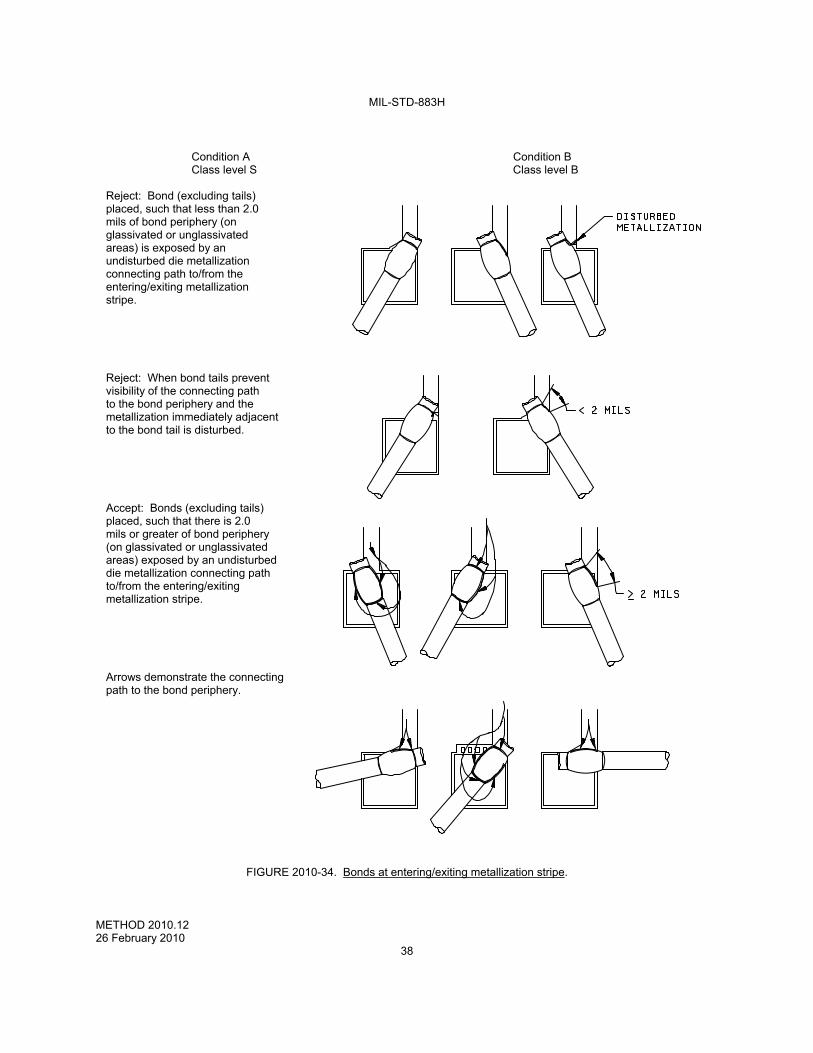
MIL-STD-883H
METHOD 2010.12 26 February 2010
38
Condition A Condition B
Class level S Class level B Reject: Bond (excluding tails) placed, such that less than 2.0 mils of bond periphery (on glassivated or unglassivated areas) is exposed by an undisturbed die metallization connecting path to/from the entering/exiting metallization stripe.
Reject: When bond tails prevent visibility of the connecting path to the bond periphery and the metallization immediately adjacent to the bond tail is disturbed.
Accept: Bonds (excluding tails) placed, such that there is 2.0 mils or greater of bond periphery (on glassivated or unglassivated areas) exposed by an undisturbed die metallization connecting path to/from the entering/exiting metallization stripe.
Arrows demonstrate the connecting path to the bond periphery.
FIGURE 2010-34. Bonds at entering/exiting metallization stripe.
MIL-STD-883H
METHOD 2010.12 26 February 2010
39
Condition A Condition B
Class level S Class level B
h. Bonds where more than 25 percent of the bond is located on die mounting material.
i. Any evidence of repair of conductors by bridging with additional material.
j. Bonds on foreign material.
k. Intermetallic formation extending radially more than 0.1 mil completely around the periphery of that portion of the gold bond located on metal.
3.2.1.5 Rebonding of monolithic devices. Rebonding of monolithic microcircuits, may be done with the following
limitations. No device shall be acceptable that exhibits:
a. Rebond over exposed passivation or over metal which shows evidence of peeling. More than one rebond attempt at any design bond location. Rebonds that touch an area of exposed oxide caused by lifted metal.
b. A bond on top of, or partially on top of, another b. Bond along side or partially on top of bond, bond wire tail, or residual segment of wire. another bond, bond wire tail or residual segment of wire, when the overlap width is greater than 25 percent.
c. Rebond attempts that exceed 10 percent of the total number of bonds in the microcircuit. (e.g., for a 28 lead wire
bonded package there are 56 bonds. A bond of one end of a wire shall count as a single attempt. A replacement of a wire bonded at both ends, counts as two rebond attempts.)
NOTE: For class level B only. Bond-offs required to
clear the bonder after an unsuccessful first bond attempt are not considered as rebonds provided they can be identified as bond-offs.
d. Missing or extra wires. 3.2.1.6 Flip chip solder bump die. No solder bumped die shall be acceptable that exhibit any of the following
characteristics (see figure 2010-34A):
a. missing solder ball from original design position. b. Solder ball 20% smaller, or larger than design size (nominal). c. Solder balls bridging. d. Any attached or embedded foreign material bridging balls, or redistribution metalization. e. Misaligned solder ball which exposes the UBM on the contact via. f. Voids in redistribution metalization greater than 50% of the design width. g. Any redistribution metalization bridging. h. Any residual unetched UBM bridging balls or redistribution metalization. i. Mechanical damage to the ball which reduces the original height or diameter more than 20%. j. Lifting, or peeling or the RDL or dielectric material.
Note: Minor damage to the solder ball and bump misalignment can be reworked by performing a re-flow/refresh of the
solder balls.

MIL-STD-883H
METHOD 2010.12 26 February 2010
40
Figure 2010.34A – FLIP CHIP VISUAL INSPECTION DIAGRAM
MIL-STD-883H
METHOD 2010.12 26 February 2010
41
Condition A Condition B
Class level S Class level B 3.2.2 Internal wires. During inspection for the requirements of 3.2.2, each device shall be viewed at any angle necessary
to determine full compliance to this specification, without damaging the device. No device shall be acceptable that exhibits:
a. Any wire with a separation of less than two wire a. Any wire with a separation of less than one diameters to unglassivated operating metal,other wire diameter to unglassivated operating bonds, another wire (common wires excluded),other metal, other bonds, another wire (common package post, unglassivated die area (except for wires excluded), other package post, wires or pads which are at the die or substrate unglassivated die area (except for wires or potential), or any portion of the package pads which are at the die or substrate including the plane of the lid to be attached. potential), or any conductive portion of the package or the plane of the lid to be attached.
NOTE: For condition A only. Within a 5.0 mil NOTE: For condition B only. Within a radial distance from the perimeter of the bond 10.0 mil radial distance from the perimeter on the die the separation shall be 1.0 mil of the bond on the die a line of separation minimum. must be visible.
NOTE: For SOS devices, exclude the unglassivated insulator areas.
b. Nicks, bends, cuts, crimps, scoring, or neckdown in any wire that reduces the wire diameter by more than 25
percent.
c. Tearing at the junction of the wire and bond.
d. Any wire making a straight line run from a die bonding pad to a package post that has no arc.
MIL-STD-883H
METHOD 2010.12 26 February 2010
42
Condition A Condition B
Class level S Class level B
e. Wire(s) crossing wire(s) when viewed from above, e. Wire(s) crossing wire(s) when viewed from above, (excluding common conductors) except in multitiered (excluding common conductors) except that wires packages, where the crossing occurs within the crossing wires bonded to package posts that are boundary of the lower wire bond tier(s) being crossed at difference heights, or wires bonded into the or packages with down bond(s). In these situations, package cavity that cross are acceptable if they the wires that cross are acceptable if they maintain maintain a minimum clearance of two wire diameters a minimum clearance of two wire diameters (see figure (e.g., multitiered packages or packages with down 2010-35). bond chips).
NOTE: No bond wire shall cross more than one other bond wire and there shall be no more than 4 crossovers or crossovers involving more than 10 percent of the total number of wires, whichever is greater for any single package cavity.
f. Wire(s) not in accordance with bonding diagram.
3.2.3 Die mounting.
3.2.3.1 Die mounting eutectic. No device shall be acceptable that exhibits:
a. Die mounting material buildup that extends onto the top surface or extends vertically above the top surface of the die.
b. Die mounting material (eutectic wetting) not visible around at least two complete sides or 75 percent of the die
perimeter, except for transparent die.
c. Transparent die with less than 50 percent of the area bonded.
d. Flaking of the die mounting material.
e. Balling or buildup of the die mounting material that does not exhibit a minimum of 50 percent peripheral fillet when viewed from above or the accumulation of die mounting material is such that the height of the accumulation is greater than the longest base dimension or the accumulation necks down at any point (see figure 2010-36).
MIL-STD-883H
METHOD 2010.12 26 February 2010
43
FIGURE 2010-35. Class level S criteria for wire(s) crossing wire(s).
MIL-STD-883H
METHOD 2010.12 26 February 2010
44
FIGURE 2010-36. Balling of die attach material.
MIL-STD-883H
METHOD 2010.12 26 February 2010
45
Condition A Condition B Class level S Class level B
3.2.3.2 Die mounting noneutectic. No device shall be acceptable that exhibits:
a. Adhesive material immediately adjacent to the die that extends onto or vertically above the top surface of the die.
b. Adhesive fillet not visible along 75 percent of each side of the die. c. Any flaking, peeling, or lifting of the adhesive material.
d. Separation, cracks, or fissures greater than or equal to 2 mils in width in the adhesive at the cavity wall or cavity
floor.
e. Crazing in the adhesive.
f. Adhesive material on the top surface of the die.
g. Adhesive that bridges package posts or is on the post bond area.
h. Any adhesive material that is connected to the fillet or conductive cavity (e.g. metal package base or metallized floor of ceramic package), and extends up the cavity wall to within 1.0 mil of the package post.
i. Transparent die with less than 50 percent of the area bonded.
3.2.3.3 Die orientation. No device shall be acceptable that exhibits:
a. Die not located or oriented in accordance with the applicable assembly drawing.
b. Die that appears to be obviously tilted (i.e., more than 10 degrees) with respect to the package cavity.
3.2.4 Beam lead construction.
3.2.4.1 Bonds. This inspection criteria shall apply to the completed bond area made, using either direct tool contact or a
compliant intermediate layer. No device shall be acceptable that exhibits:
a. Bonds where the tool impression does not completely cross the entire beam width.
b. Bonds on thin film substrate metal where the tool impression increases the beam lead width less than 15 percent (10 percent for compliant bonds) or greater than 75 percent of the undeformed beam width.
c. Bonds where the tool impression length is less than 1.0 mil (see figure 2010-37). d. Bonding tool impression less than 1.0 mil from the die edge (see figure 2010-37).
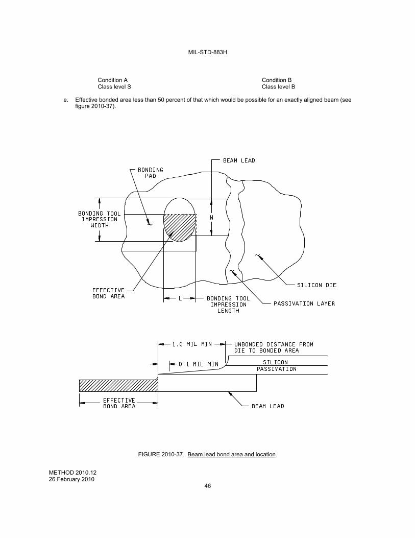
MIL-STD-883H
METHOD 2010.12 26 February 2010
46
Condition A Condition B
Class level S Class level B
e. Effective bonded area less than 50 percent of that which would be possible for an exactly aligned beam (see figure 2010-37).
FIGURE 2010-37. Beam lead bond area and location.
MIL-STD-883H
METHOD 2010.12 26 February 2010
47
Condition A Condition B
Class level S Class level B
f. Cracks or tears in the effective bonded area of the beam greater than 50 percent of the original beam width.
g. Bonds placed so that the separation between bonds and between bonds and operating metallization not connected to them is less than 0.1 mil.
h. Bonds lifting or peeling.
3.2.4.2 Beam leads. No device shall be acceptable that exhibits the following:
a. Voids, nicks, depressions, or scratches that leave less than 50 percent of the beam width undisturbed.
b. Beam separation from the die.
c. Missing or partially fabricated beam leads unless by design.
d. Beam leads that are not bonded.
e. Bonded area closer than 0.1 mil to the edge of the passivation layer.
f. Less than 0.1 mil passivation layer between the die and the beam visible at both edges of the beam (see figure
2010-37 and 2010-38).
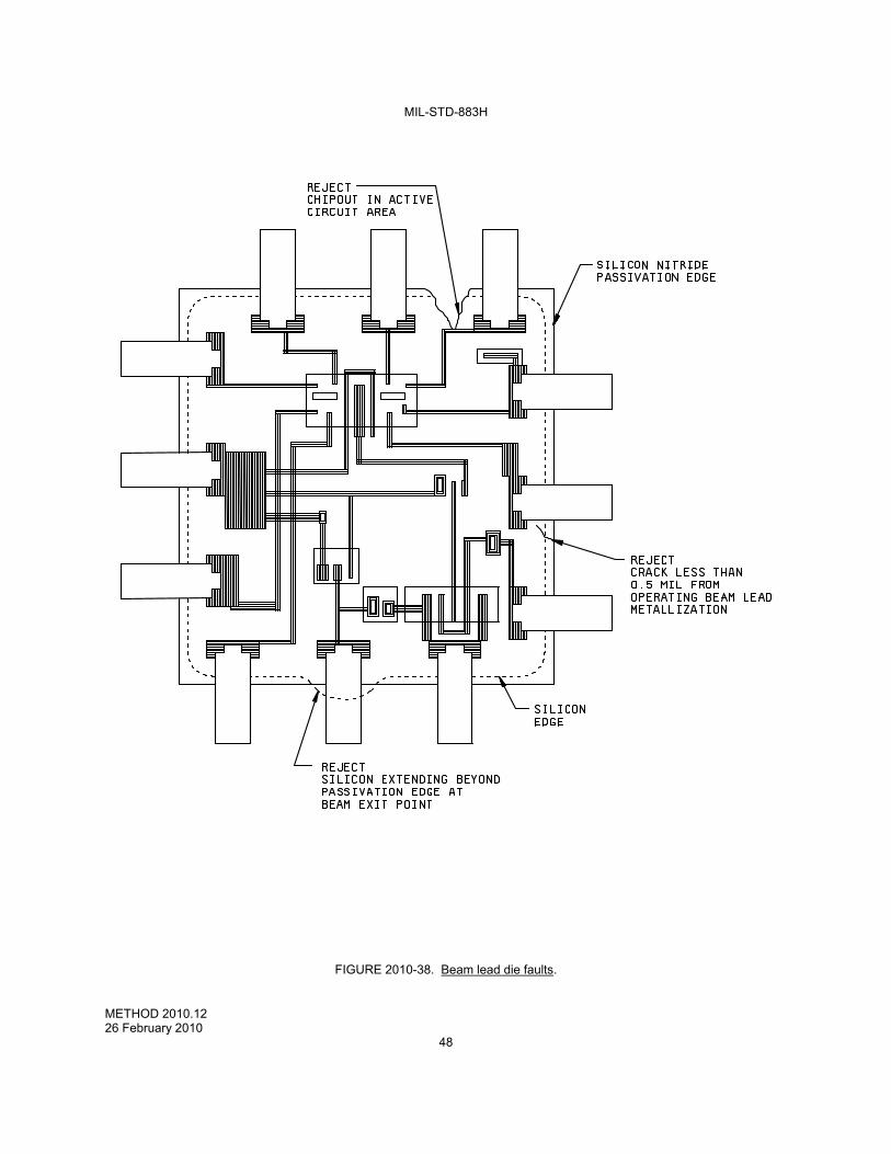
MIL-STD-883H
METHOD 2010.12 26 February 2010
48
FIGURE 2010-38. Beam lead die faults.
MIL-STD-883H
METHOD 2010.12 26 February 2010
49
Condition A Condition B
Class level S Class level B 3.2.5 Foreign material. Die inspections shall be at high magnification. Package and lid inspections shall be at low
magnification. Die criteria may be examined at high magnification prior to die mounting provided they are re-examined at low magnification during preseal inspection. No device shall be acceptable that exhibits: NOTE: Foreign material may be removed, if possible, by subjecting the device to a nominal gas blow (less than 25 psig).
After this gas blow off at inspection, all wire bonded devices shall be inspected/reinspected for possible wire damage. Use of a higher psig value is permitted provided that the manufacturer has characterized the process and has data to assure that no damage is done to the wire bonds. This data shall be available upon request to the preparing or acquiring activities.
a. Foreign particle(s) on the surface of the die that is (are) large enough to bridge the narrowest spacing between
unglassivated operating material (e.g., metallization, bare semiconductor material, mounting material, bonding wire, etc.).
b. Foreign particle(s) other than on the surface of the die within the package or on the lid or cap that is (are) large
enough to bridge the narrowest spacing between unglassivated operating materials and are not the following: Semiconductor material, glass splatter, gold imperfections in the die attach area, gold eutectic material or package ceramic material.
NOTE: As an alternative to 100 percent visual inspection of lids or caps, the lids or caps may be subjected to a
suitable cleaning process and quality verification, approved by the qualifying activity. The lids or caps shall subsequently be held in a controlled environment until capping or preparation for seal.
c. Foreign material attached to or embedded in the die surface that appears to bridge the active circuit elements
including metallization unless verified as only attached but not embedded by high power dark field illumination.
d. Liquid droplets, chemical stains, ink, or photoresist on the die surface that appear to bridge any combination of unglassivated metallization or bare semiconductor material areas.
e. A particle of gold eutectic material, package ceramic material or semiconductor material, not attached to the die,
large enough to bridge the narrowest spacing between unglassivated operating materials, that does not exhibit a minimum of 50 percent cumulative peripheral fillet or whose height is greater than the longest base dimension.
NOTE 1: This criteria shall not be cause for rejection when the assembly process contains a gas blow (less than 60 psig) after die attach and again Less than 25 psig) after wire bond provided rejectable materials (not attached and large enough to bridge) have been removed from the cavity.
NOTE 2: Gold imperfections in the die attach area that do not interfere with proper die attachment, sealing glass splatter
(provided it does not suggest inadequately controlled process and does not interfere with the die attach area) or internal glass run out from frit seal (provided it is confined to package walls and does not interfere with the die attach area) are not rejectable.
MIL-STD-883H
METHOD 2010.12 26 February 2010
50
Condition A Condition B
Class level S Class level B 3.2.5.1 Foreign material, die coated devices. This inspection and criteria shall be required on all devices that receive a
die coat during the assembly process. This inspection will be done after die coat cure. No device shall be acceptable that exhibits:
a. Unattached foreign particles on the surface of the die coat or within the package that is (are) large enough to bridge the narrowest spacing between unglassivated operating material (e.g., metallization, bare semiconductor material, mounting material, bonding wire, etc.). Note: Semiconductor particles shall be considered as foreign material.
b. Partially embedded foreign material with an "unembedded portion" that is large enough to bridge the narrowest
spacing between unglassivated operating material (e.g., metallization, bare semiconductor material, mounting material, bonding wire, etc.).
c. Foreign material attached to or embedded in the die coat that appears to bridge unglassivated operating material
when viewed from above (e.g., bare semiconductor material, bond pads, bonding wire, mounting material, etc.).
d. Embedded foreign particles that penetrate the entire thickness of the die coating. 3.2.5.1.1 Die coating material. No device shall be accepted that exhibits:
a. Surface scratches that penetrate the die coating and expose underlying glassivated metal.
b. Die coating that is lifted or is peeling from the semiconductor surface. 3.2.6 GaAs backside metallization. GaAs inspection shall be performed with low magnification prior to die mounting.
(Verification at high magnification is permitted.) With the approval of the acquiring activity, the manufacturer may substitute a sample inspection plan at the wafer level for 100 percent inspection in dice form. The sample inspection plan shall be documented in the manufacturer's baseline documentation and shall be performed to the requirements of test method 5013. No devices shall be acceptable that exhibit the following.
a. Evidence of metal corrosion, lifting, peeling, blistering.
b. Voids or scratches that expose underlying metal or substrate whose cumulative areas are more than 25 percent of
the cell area or device area.
NOTE: Absence of gold in the die separation area (saw street) of devices with electroplated backside metallization is not a cause for rejection. Small voids at edges due to die separation are acceptable if they comprise less than 10 percent of the backside area.
c. Any voids or scratches in the substrate via metallization that effects more than 25 percent of the metallization or
cause unintended isolation of the metallization path.
d. Underetched vias.
e. Overetched vias.
4. SUMMARY. The following details shall be specified in the applicable acquisition document.
a. Test condition (see 3). b. Where applicable, any conflicts with approved circuit design topology or construction.
c. Where applicable, gauges, drawings, and photographs that are to be used as standards for operator comparison
(see 2).
d. Where applicable, specific magnification (see 3).
MIL-STD-883H
METHOD 2011.8 26 February 2010
1
METHOD 2011.8
BOND STRENGTH (DESTRUCTIVE BOND PULL TEST)
1. PURPOSE. The purpose of this test is to measure bond strengths, evaluate bond strength distributions, or determine compliance with specified bond strength requirements of the applicable acquisition document. This test may be applied to the wire-to-die bond, wire-to-substrate bond, or the wire-to-package lead bond inside the package of wire-connected microelectronic devices bonded by soldering, thermocompression, ultrasonic, or related techniques. It may also be applied to bonds external to the device such as those from device terminals-to-substrate or wiring board or to internal bonds between die and substrate in non-wire-bonded device configurations such as beam lead or flip chip devices.
2. APPARATUS. The apparatus for this test shall consist of suitable equipment for applying the specified stress to the bond, lead wire or terminal as required in the specified test condition. A calibrated measurement and indication of the applied stress in grams force (gf) shall be provided by equipment capable of measuring stresses up to twice the specified minimum limit value, with an accuracy of ±5 percent or ±0.3 gf, whichever is the greater tolerance.
3. PROCEDURE. The test shall be conducted using the test condition specified in the applicable acquisition document consistent with the particular device construction. All bond pulls shall be counted and the specified sampling, acceptance, and added sample provisions shall be observed, as applicable. Unless otherwise specified, for conditions A, C, and D, the sample size number specified for the bond strength test shall determine the minimum sample size in terms of the minimum number of bond pulls to be accomplished rather than the number of complete devices in the sample, except that the required number of bond pulls shall be randomly selected from a minimum of 4 devices. Bond pulls in accordance with test conditions D, F, G, and H, while involving two or more bonds shall count as a single pull for bond strength and sample size number purposes. Unless otherwise specified, for conditions F, G, and H the sample size number specified shall determine the number of die to be tested (not bonds). For hybrid or multichip devices (all conditions), a minimum of 4 die or use all die if four are not available on a minimum of 2 completed devices shall be used. Where there is any adhesive, encapsulant or other material under, on or surrounding the die such as to increase the apparent bond strength, the bond strength test shall be performed prior to application. The stress required to achieve bond failure shall be observed and the physical location of the point of failure shall be recorded as being in one of the listed categories (see 3.2.1). When flip chip or beam-lead chips are bonded to substrates other than those in completed devices, the following conditions shall apply:
a. The sample of chips for this test shall be taken at random from the same chip population as that used in the completed devices that they are intended to represent.
b. The chips for this test shall be bonded on the same bonding apparatus as the completed devices, during the time
period within which the completed devices are bonded.
c. The test chip substrates shall be processed, metallized, and handled identically with the completed device substrates, during the same time period within which the completed device substrates are processed.
3.1 Test conditions:
3.1.1 Test condition A - Bond peel. This test is normally employed for bonds external to the device package. The lead or
terminal and the device package shall be gripped or clamped in such a manner that a peeling stress is exerted with the specified angle between the lead or terminal and the board or substrate. Unless otherwise specified, an angle of 90 degrees shall be used. When a failure occurs, the force causing the failure and the failure category shall be recorded.
3.1.2 Test condition C - Wire pull (single bond). This test is normally employed for internal bonds at the die or substrate and the lead frame of microelectronic devices. The wire connecting the die or substrate shall be cut so as to provide two ends accessible for pull test. In the case of short wire runs, it may be necessary to cut the wire close to one termination in order to allow pull test at the opposite termination. The wire shall be gripped in a suitable device and simple pulling action applied to the wire or to the device (with the wire clamped) in such a manner that the force is applied approximately normal to the surface of the die or substrate. When a failure occurs, the force causing the failure and the failure category shall be recorded.
*
*
MIL-STD-883H
METHOD 2011.8 26 February 2010
2
3.1.3 Test condition D - Wire pull (double bond). This procedure is identical to that of test condition C, except that the pull is applied by inserting a hook under the lead wire (attached to die, substrate or header or both ends) with the device clamped and hook contacting the wire between midspan and loop apex, without causing adverse wire deformation (for forward wedge and ball bonding, this would be between midspan and the die edge: for reverse bonding, this would be between midspan and the package edge) and the pulling force is applied in a perpendicular direction to the die or substrate surface. See Figure 2011-1. When a failure occurs, the force causing the failure and the failure category shall be recorded. The minimum bond strength shall be taken from table I. Figure 2011-2 may be used for wire diameters not specified in table I. For wire diameter or equivalent cross section >0.005 inch, where a hook will not fit under the wire, a suitable clamp can be used in lieu of a hook.
3.1.4 Test condition F - Bond shear (flip chip). This test is normally employed for internal bonds between a semiconductor die and a substrate to which it is attached in a face-bonded configuration. It may also be used to test the bonds between a substrate and an intermediate carrier or secondary substrate to which the die is mounted. A suitable tool or wedge shall be brought in contact with the die (or carrier) at a point just above the primary substrate and a force applied perpendicular to one edge of the die (or carrier) and parallel to the primary substrate, to cause bond failure by shear. When a failure occurs, the force at the time of failure, and the failure category shall be recorded.
3.1.5 Test condition G – Push-off test (beam lead). This test is normally employed for process control and is used on a sample of semiconductor die bonded to a specially prepared substrate. Therefore, it cannot be used for random sampling of production or inspection lots. A metallized substrate containing a hole shall be employed. The hole appropriately centered, shall be sufficiently large to provide clearance for a push tool, but not large enough to interfere with the bonding areas. The push tool shall be sufficiently large to minimize device cracking during testing, but not large enough to contact the beam leads in the anchor bond area. Proceed with push-off tests as follows: The substrate shall be rigidly held and the push tool inserted through the hole. The contact of the push tool to the silicon device shall be made without appreciable impact (less than 0.01 inch/minute (0.254 mm/minute ) and forced against the underside of the bonded device at a constant rate. When failure occurs, the force at the time of failure, and the failure category shall be recorded.
3.1.6 Test condition H – Pull-off test (beam lead). This test is normally employed on a sample basis on beam lead devices which have been bonded down on a ceramic or other suitable substrate. The calibrated pull-off apparatus (see 2) shall include a pull-off rod (for instance, a current loop of nichrome or Kovar wire) to make connection with a hard setting adhesive material (for instance, heat sensitive polyvinyl acetate resin glue) on the back (top side) of the beam lead die. The substrate shall be rigidly installed in the pull-off fixture and the pull-off rod shall make firm mechanical connection to the adhesive material. The device shall be pulled within 5 degrees of the normal to at least the calculated force (see 3.2), or until the die is at 2.54 mm (0.10 inch) above the substrate. When a failure occurs, the force at the time of failure, the calculated force limit, and the failure category shall be recorded.
3.1.7 Wire Ball Bond Shear. Procedure in accordance with EIA/JESD22-B116 Wire Bond Shear Test Method.
3.2 Failure criteria. Any bond pull which results in separation under an applied stress less than that indicated in table I as the required minimum bond strength for the indicated test condition, composition, and construction shall constitute a failure. 3.2.1 Failure category. Failure categories are as follows: When specified, the stress required to achieve separation and the category of separation or failure shall be recorded.
a. For internal wire bonds:
(a-1) Wire break at neckdown point (reduction of cross section due to bonding process). (a-2) Wire break at point other than neckdown. (a-3) Failure in bond (interface between wire and metallization) at die. (a-4) Failure in bond (interface between wire and metallization) at substrate, package post, or other than die. (a-5) Lifted metallization from die.
*
*
*
MIL-STD-883H
METHOD 2011.8 26 February 2010
3
(a-6) Lifted metallization from substrate or package post. (a-7) Fracture of die. (a-8) Fracture of substrate.
b. For external bonds connecting device to wiring board or substrate:
(b-1) Lead or terminal break at deformation point (weld affected region).
(b-2) Lead or terminal break at point not affected by bonding process.
(b-3) Failure in bond interface (in solder or at point of weld interface between lead or terminal and the board or
substrate conductor to which the bond was made).
(b-4) Conductor lifted from board or substrate.
(b-5) Fracture within board or substrate.
c. For flip-chip configurations:
(c-1) Failure in the bond material or pedestal, if applicable.
(c-2) Fracture of die (or carrier) or substrate (removal of portion of die or substrate immediately under the bond).
(c-3) Lifted metallization (separation of metallization or bonding pedestal from die (or carrier) or substrate.
d. For beam lead devices:
(d-1) Silicon broken.
(d-2) Beam lifting on silicon.
(d-3) Beam broken at bond.
(d-4) Beam broken at edge of silicon. (d-5) Beam broken between bond and edge of silicon. (d-6) Bond lifted.
(d-7) Lifted metallization (separation of metallization) from die, separation of bonding pad.
(d-8) Lifted metallization.
NOTE: RF/microwave hybrids that require extremely flat loops which may cause erroneous wire pull data may use the
following formula to determine the proper wire pull value. V1 = V2 sin Where: V1 = New value to pull test. V2 = Table I value for size wire tested. = Greatest calculated wire loop angle (Figure 2011-3).
Also, RF/microwave hybrids that contain wires that cannot be accessed with a pull hook must be duplicated on a test coupon in such a way to allow hook access for purposes of pull testing. These wires are to be bonded at the same time the production hybrids are bonded using the same setup, operator, and schedule. The test coupon wires are to be pull tested in lieu of the tuning or inaccessible wires on the production hybrid. Failures on the test coupon shall be considered as failures to production units and appropriate action is to be taken in accordance with the applicable specification (Figure 2011-4).
*
*
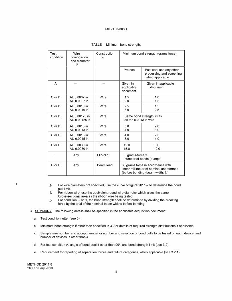
MIL-STD-883H
METHOD 2011.8 26 February 2010
4
TABLE I. Minimum bond strength.
Test condition
Wire composition and diameter 1/
Construction 2/
Minimum bond strength (grams force)
Pre seal Post seal and any other processing and screening when applicable
A --- --- Given in applicable document
Given in applicable document
C or D AL 0.0007 in AU 0.0007 in
Wire 1.5 2.0
1.0 1.5
C or D AL 0.0010 in AU 0.0010 in
Wire 2.5 3.0
1.5 2.5
C or D AL 0.00125 in AU 0.00125 in
Wire Same bond strength limits as the 0.0013 in wire
C or D AL 0.0013 in AU 0.0013 in
Wire 3.0 4.0
2.0 3.0
C or D AL 0.0015 in AU 0.0015 in
Wire 4.0 5.0
2.5 4.0
C or D AL 0.0030 in AU 0.0030 in
Wire 12.0 15.0
8.0 12.0
F Any Flip-clip 5 grams-force x number of bonds (bumps)
G or H Any Beam lead 30 grams force in accordance with linear millimeter of nominal undeformed (before bonding) beam width. 3/
1/ For wire diameters not specified, use the curve of figure 2011-2 to determine the bond pull limit. 2/ For ribbon wire, use the equivalent round wire diameter which gives the same Cross-sectional area as the ribbon wire being tested. 3/ For condition G or H, the bond strength shall be determined by dividing the breaking force by the total of the nominal beam widths before bonding.
4. SUMMARY. The following details shall be specified in the applicable acquisition document:
a. Test condition letter (see 3).
b. Minimum bond strength if other than specified in 3.2 or details of required strength distributions if applicable.
c. Sample size number and accept number or number and selection of bond pulls to be tested on each device, and number of devices, if other than 4.
d. For test condition A, angle of bond peel if other than 90, and bond strength limit (see 3.2). e. Requirement for reporting of separation forces and failure categories, when applicable (see 3.2.1).
*
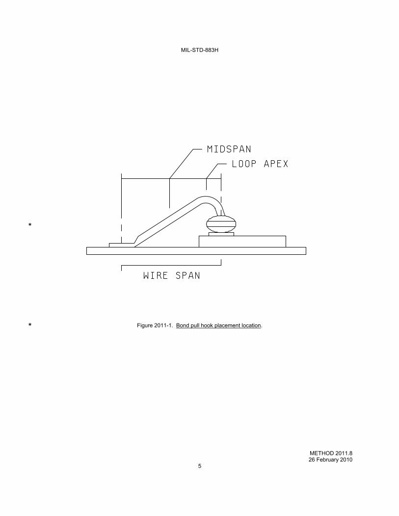
MIL-STD-883H
METHOD 2011.8 26 February 2010
5
Figure 2011-1. Bond pull hook placement location.
*
*
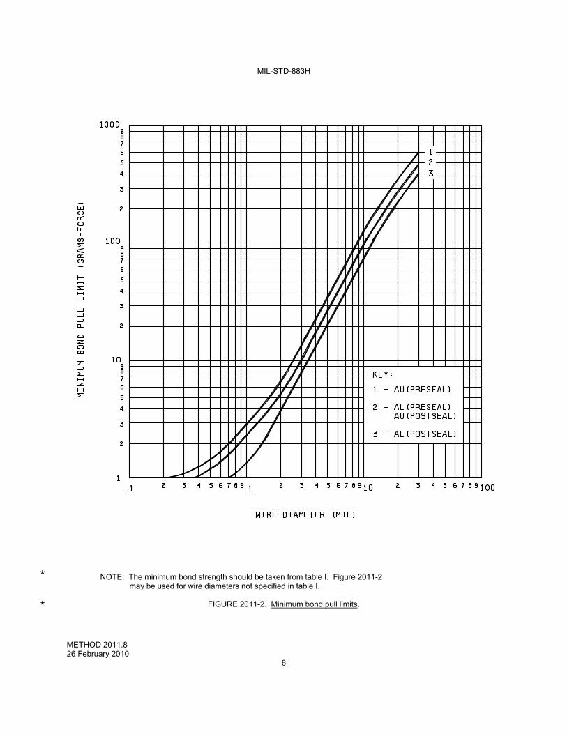
MIL-STD-883H
METHOD 2011.8 26 February 2010
6
NOTE: The minimum bond strength should be taken from table I. Figure 2011-2
may be used for wire diameters not specified in table I.
FIGURE 2011-2. Minimum bond pull limits.
*
*

MIL-STD-883H
METHOD 2011.8 26 February 2010
7
FIGURE 2011-3. Wire loop angle.
FIGURE 2011-4. Flat loop wire pull testing.
*
*

MIL-STD-883H
METHOD 2011.8 26 February 2010
8
This page intentionally left blank
MIL-STD-883H
METHOD 2012.8 26 February 2010
1
METHOD 2012.8 RADIOGRAPHY
1. Purpose. The purpose of this examination is to nondestructively detect defects within the sealed case, especially those resulting from the sealing process and internal defects such as foreign objects, improper interconnecting wires, and voids in the die attach material or in the glass when glass seals are used. It establishes methods, criteria, and standards for radiographic examination of semiconductor and hybrid devices.
NOTE: For certain device types, opacity of the construction materials (packages or internal attachment) may effectively prevent radiographic identification of certain types of defects from some or all possible viewing angles. This factor should be considered in relation to the design of each device when application of this test method is specified.
2. Apparatus. The apparatus and material for this test shall include:
a. Radiographic equipment with a sufficient voltage range to penetrate the device. The focal distance shall be adequate to maintain a sharply defined image of an object with a major dimension of 0.0254 mm (0.001 inch).
b. Radiographic film: Very fine grain industrial X-ray film grade, either single or double emulsion.
c. Radiographic viewer: Capable of 0.0254 mm (0.001 inch) resolution in major dimension.
d. Holding fixtures: Capable of holding devices in the required positions without interfering with the accuracy or ease
of image interpretation.
e. Radiographic quality standards: Capable of verifying the ability to detect all specified defects.
f. Film holder: A 1.6 mm (0.0625 inch) minimum lead-topped table or lead-backed film holders to prevent back scatter of radiation.
3. Procedure. The X-ray exposure factors, voltage, milliampere and time settings shall be selected or adjusted as
necessary to obtain satisfactory exposures and achieve maximum image details within the sensitivity requirements for the device or defect features the radiographic test is directed toward. The X-ray voltage shall be the lowest consistent with these requirements and shall not exceed 200 kV.
3.1 Mounting and views. The devices shall be mounted in the holding fixture so that the devices are not damaged or contaminated and are in the proper plane as specified. The devices may be mounted in any type of fixture and masking with lead diaphragms or barium clay may be employed to isolate multiple specimens provided the fixtures or masking material do not block the view from X-ray source to the film of any portion of the body of the device.
3.1.1 Views.
3.1.1.1 Flat packages, dual-in-line packages, hybrid packages, and single ended cylindrical devices. Flat packages, dual-in-line packages, hybrid packages, and single ended cylindrical devices, unless otherwise specified, shall have one view taken with the X-rays penetrating in the Y direction as defined on figures 1 and 2 of MIL-STD-883, GENERAL REQUIREMENTS. When more than one view is required, the second and third views, as applicable, shall be taken with the X-rays penetrating in the Z and X direction respectively (either Z or X for flat packages). The die/cavity interface shall be positioned as close as possible to the film to avoid distortion.
*
MIL-STD-883H
METHOD 2012.8 26 February 2010
2
3.1.1.2 Stud-mounted and cylindrical axial lead devices. Stud-mounted and cylindrical axial lead devices, unless otherwise specified, shall have one view taken with the X-rays penetrating in the X direction as defined on figures 1 and 2 of MIL-STD-883, GENERAL REQUIREMENTS. When more than one view is required, the second and third views, as applicable, shall be taken with the X-rays penetrating in the Z direction and at 45 between the X and Z direction. The die/cavity interface shall be positioned as close as possible to the film to avoid distortion.
3.2 Radiographic quality standard. Each radiograph shall have at least two quality standards exposed with each view, located (and properly identified) in opposite corners of the film. These penetrameters shall be of a radiographic density nearest the density of the devices being inspected. The radiographic quality standard shall consist of a suitable ASTM penetrameter as described in the DOD adopted standard ASTM E 801 Standard Practice for Controlling Quality of Radiographic Testing of Electronic Devices, or equivalent.
3.3 Film and marking. The radiographic film shall be in a film holder backed with a minimum of 1/16 inch lead or the holder shall be placed on the lead topped table. The film shall be identified using techniques that print the following information, photographically, on the radiograph:
a. Device manufacturer's name or code identification number.
b. Device type or Part or Identifying Number.
c. Production lot number or date code or inspection lot number.
d. Radiographic film view number and date.
e. Device serial or cross reference numbers, when applicable.
f. X-ray laboratory identification, if other than device manufacturer.
3.3.1 Nonfilm techniques and real time x-ray. The use of nonfilm techniques and real time x-ray is permitted if the equipment is capable of producing results of equal quality when compared with film techniques, and all requirements of this method are complied with, except those pertaining to the actual film. Radiographic quality standards, as specified in 3.2, may be used at the beginning and end of each inspection lot if equipment settings are not modified.
3.3.2 Serialized devices. When device serialization is required, each device shall be readily identified by a serial
number. They shall be radiographed in consecutive, increasing serial order. When a device is missing, the blank space shall contain either the serial number or other X-ray opaque object to readily identify and correlate X-ray data. When large skips occur within serialized devices, the serial number of the last device before the skip and the first device after the skip may be used in place of the multiple opaque objects.
3.3.3 Special device marking. When specified (see 4.c), the devices that have been X-rayed and found acceptable shall be identified with a blue dot on the external case. The blue dot shall be approximately 1.6 mm (0.0625 inch) in diameter. The color selected from FED-STD-595 shall be any shade between 15102-15123 or 25102-25109. The dot shall be placed so that it is readily visible but shall not obliterate other device marking.
3.4 Tests. The X-ray exposure factor shall be selected to achieve resolution of 0.0254 mm (0.001 inch) major dimension, less than 10 percent distortion and an "H" and "D" film density between 1 and 2.5 in the area of interest of the device image. Radiographs shall be made for each view required (see 4).
3.5 Processing. The radiographic film manufacturer's recommended procedure shall be used to develop the exposed film, and film shall be processed so that it is free of processing defects such as fingerprints, scratches, fogging, chemical spots, blemishes, etc.
*
MIL-STD-883H
METHOD 2012.8 26 February 2010
3
3.6 Operating personnel. Personnel who will perform radiographic inspection shall have training in radiographic procedures and techniques so that defects revealed by this method can be validly interpreted and compared with applicable standards. The following minimum vision requirements shall apply for personnel inspecting film:
a. Distant vision shall equal at least 20/30 in both eyes, corrected or uncorrected.
b. Near vision shall be such that the operator can read Jaeger type No. 2 at a distance of 16 inches, corrected or uncorrected.
c. Vision tests shall be performed by an oculist, optometrist, or other professionally recognized personnel at least
once a year. Personnel authorized to conduct radiographic tests shall be required to pass the vision test specified in 3.6 a and b.
3.7 Personnel safety precautions. The safety precautions described in National Council on Radiation Protection and
Measurements Report Number 102 – Medical X-ray, Electron Beam and Gamma Ray Protection for Energies Up to 50MeV and Report Number 040 – Protection Against Radiation from Brachytherapy Sources shall be complied with when applicable.
3.8 Interpretation of radiographs. Utilizing the equipment specified herein, radiographs shall be inspected to
determine that each device conforms to this standard and defective devices shall be rejected. Interpretation of the radiograph shall be made under low light level conditions without glare on the radiographic viewing surface. The radiographs shall be examined on a suitable illuminator with variable intensity or on a viewer suitable for radiographic inspection on projection type viewing equipment. The radiograph shall be viewed at a magnification between 6X and 25X. Viewing masks may be used when necessary. Any radiograph not clearly illustrating the features in the radiographic quality standards is not acceptable and another radiograph of the devices shall be taken. 3.9 Reports of records.
3.9.1 Reports of inspection. For class S devices, or when specified for other device classes, the manufacturer shall furnish inspection reports with each shipment of devices. The report shall describe the results of the radiographic inspection, and list the purchase order number or equivalent identification, the PIN, the date code, the quantity inspected, the quantity rejected, and the date of test and which devices utilize the note in 3.10.2.1. For each rejected device, the PIN, the serial number, when applicable, and the cause for rejection shall be listed.
3.9.2 Radiograph submission. Photographic reproduction of complete radiographs may be submitted, but artistic renditions are not acceptable.
3.9.3 Radiograph and report retention. When specified, the manufacturer shall retain a set of the radiographs and a copy of the inspection report. These shall be retained for the period specified.
3.10 Examination and acceptance criteria for monolithic devices.
3.10.1 Device construction. Acceptable devices shall be of the specified design and construction with regard to the characteristics discernible through radiographic examination. Devices that deviate significantly from the specified construction shall be rejected.
3.10.2 Individual device defects. The individual device examination shall include, but not be limited to, inspection for foreign particles, solder or weld "splash", build-up of bonding material, proper shape and placement of lead wires or whiskers, bond of lead or whisker to semiconductor element and lead or whisker to terminal post, semiconductor metallization pattern, and mounting of semiconductor element. Any device for which the radiograph reveals any of the following defects shall be rejected:
*
MIL-STD-883H
METHOD 2012.8 26 February 2010
4
3.10.2.1 Presence of extraneous matter. Extraneous matter (foreign particles) shall include, but not be limited to:
a. Any foreign particle, loose or attached, greater than 0.025 mm (0.001 inch) (see figure 2012-1), or of any lesser size which is sufficient to bridge nonconnected conducting elements of the semiconductor device.
b. Any wire tail extending beyond its normal end by more than two wire diameters at the semiconductor die pad or by
more than four wire diameters at the semiconductor package post (see figure 2012-1).
c. Any burr on a post (header lead) greater than 0.08 mm (0.003 inch) in its major dimension or of such configuration that it may break away.
d. Excessive semiconductor element bonding material build-up.
(1) A semiconductor element shall be mounted and bonded so that it is not tilted more than 10° from the normal
mounting surface. The bonding agent that accumulates around the perimeter of the semiconductor element whether or not it touches the side of the semiconductor element shall not accumulate to a thickness greater than the height of the semiconductor element (see figures 2012-2 and 2012-3), or any lead or post, or be separated from the main bonding material area (see 2012-7).
(2) There shall be no visible extraneous material 0.025 mm (0.001 inch) or larger in the major
dimension inside the semiconductor device. Loose bonding material will be considered extraneous material. Excessive (but not loose) bonding material will not be considered extraneous unless it fails to meet the requirements of 3.10.2.1.d.(1) or unless the accumulation of bonding material is such that the height of the accumulation is greater than the width of its base or that the accumulation necks down at any point (see figures 2012-2 and 2012-3).
NOTE: Devices with suspect foreign particles or extraneous material (in accordance with 3.10.2.1a and 3.10.2.1.d(2) may be verified as acceptable provided the following conditions are met:
(a) A visual inspection of the die attach area at 30X to 60X shall have been conducted prior to die
attach sufficient to assure there are no anomalies in the die attach area which could interfere with effective die attach.
(b) The precap inspection shall have been conducted 100 percent to condition A of method 2010
of MIL-STD-883 and the devices shall have been inspected and prepared for sealing in a class 100 environment.
(c) All devices with X-ray defects to other criteria of 3.10 shall have been removed from the lot.
(d) Serialized devices with less than 5 suspect foreign particles and extraneous material shall be
vibrated and shocked in accordance with PIND method 2020, condition A with the detector off.
(e) A second X-ray examination of the failed view of the serialized devices after the PIND vibration/shock shall be conducted and each individual device shall be compared to its previous X-ray record.
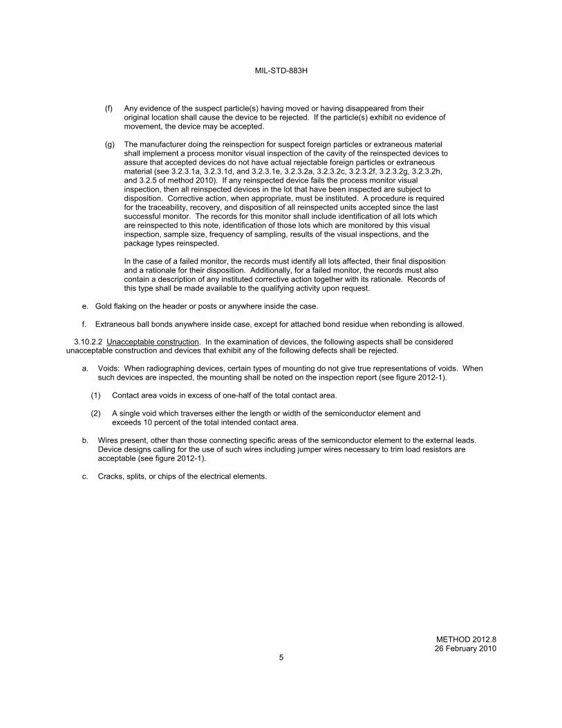
MIL-STD-883H
METHOD 2012.8 26 February 2010
5
(f) Any evidence of the suspect particle(s) having moved or having disappeared from their
original location shall cause the device to be rejected. If the particle(s) exhibit no evidence of movement, the device may be accepted.
(g) The manufacturer doing the reinspection for suspect foreign particles or extraneous material
shall implement a process monitor visual inspection of the cavity of the reinspected devices to assure that accepted devices do not have actual rejectable foreign particles or extraneous material (see 3.2.3.1a, 3.2.3.1d, and 3.2.3.1e, 3.2.3.2a, 3.2.3.2c, 3.2.3.2f, 3.2.3.2g, 3.2.3.2h, and 3.2.5 of method 2010). If any reinspected device fails the process monitor visual inspection, then all reinspected devices in the lot that have been inspected are subject to disposition. Corrective action, when appropriate, must be instituted. A procedure is required for the traceability, recovery, and disposition of all reinspected units accepted since the last successful monitor. The records for this monitor shall include identification of all lots which are reinspected to this note, identification of those lots which are monitored by this visual inspection, sample size, frequency of sampling, results of the visual inspections, and the package types reinspected.
In the case of a failed monitor, the records must identify all lots affected, their final disposition
and a rationale for their disposition. Additionally, for a failed monitor, the records must also contain a description of any instituted corrective action together with its rationale. Records of this type shall be made available to the qualifying activity upon request.
e. Gold flaking on the header or posts or anywhere inside the case. f. Extraneous ball bonds anywhere inside case, except for attached bond residue when rebonding is allowed.
3.10.2.2 Unacceptable construction. In the examination of devices, the following aspects shall be considered
unacceptable construction and devices that exhibit any of the following defects shall be rejected.
a. Voids: When radiographing devices, certain types of mounting do not give true representations of voids. When such devices are inspected, the mounting shall be noted on the inspection report (see figure 2012-1).
(1) Contact area voids in excess of one-half of the total contact area.
(2) A single void which traverses either the length or width of the semiconductor element and
exceeds 10 percent of the total intended contact area.
b. Wires present, other than those connecting specific areas of the semiconductor element to the external leads. Device designs calling for the use of such wires including jumper wires necessary to trim load resistors are acceptable (see figure 2012-1).
c. Cracks, splits, or chips of the electrical elements.
MIL-STD-883H
METHOD 2012.8 26 February 2010
6
d. Excessive undercutting of the electrical elements (X and Z plane only, see figure 2012-4).
e. Defective seal: Any device wherein the integral lid seal is not continuous or is reduced from its designed sealing width by more than 75 percent. Expulsion resulting from the final sealing operation is not considered extraneous material as long as it can be established that it is continuous, uniform and attached to the parent material and does not exhibit a ball, splash or tear-drop configuration (i.e., where the base support least dimension is smaller than the dimension it is supposed to support).
f. Inadequate clearance: Acceptable devices shall have adequate internal clearance to assure that the elements
cannot contact one another or the case. No crossover shall be allowed except as permitted by 3.2.2e of method 2010 (condition A). Depending upon the case type, devices shall be rejected for the following conditions:
NOTE: Any of the following criteria for bond wires shall not apply, if the wires are not visible In the X-ray.
(1) Flat pack and dual-in-line (see figure 2012-5).
(a) Any lead wire that appears to touch or cross another lead wire or bond, (Y plane only).
(b) Any lead wire that deviates from a straight line from bond to external lead and appears to be
within 0.05 mm (.002 inch) of another bond or lead wire (Y plane only).
(c) Lead wires that do not deviate from a straight line from bond to external lead and appear to touch another wire or bond, excluding common wires, (Y plane only).
(d) Any lead wire that touches or comes within 0.05 mm (0.002 inch) of the case or external lead
to which it is not attached (X and Y plane).
(e) Any bond that is less than 0.025 mm (0.001 inch) (excluding bonds connected by a common conductor) from another bond (Y plane only).
(f) Any wire making a straight line run from die bonding pad to package post that has no arc.
(g) Lead wires that sag below an imaginary plane across the top of the die bond (X plane only)
except by design.
(2) Round or "box" transistor type (see figure 2012-6).
(a) Any lead wire that touches or comes within 0.05 mm (0.002 inch) of the case or external lead to which it is not attached (X and Y plane).
(b) Lead wires that sag below an imaginary plane across the top of the die bond (X plane only)
except by design.
(c) Any lead wire that appears to touch or cross another lead wire or bond (Y plane only).
(d) Any lead wire that deviates from a straight line from bond to external lead and appears to touch or to be within 0.05 mm (0.002 inch) of another wire or bond (Y plane only).
(e) Any bond that is less than 0.025 mm (0.001 inch) (excluding bonds connected by a common
conductor) from another bond (Y plane only).
MIL-STD-883H
METHOD 2012.8 26 February 2010
7
FIGURE 2012-1. Particle locations, pigtails, trimming wires, and voids.

MIL-STD-883H
METHOD 2012.8 26 February 2010
8
(f) Any wire making a straight line run from die bonding pad to package post that has no arc, unless specifically designed in this manner (e.g., clips or rigid connecting leads).
(g) Any internal post that is bent more than 10° from the vertical (or intended design position) or is
not uniform in length and construction or comes closer than one post diameter to another post.
(h) Where a low profile case (such as TO-46) is used, any post which comes closer to the top of the case than 20 percent of the total inside dimension between the header and the top of the case. In devices which have the semiconductor element vertical to the header, any device where the semiconductor element comes closer than 0.05 mm (0.002 inch) to the header or to any part of the case.
(i) Any case which does not have a header design incorporating a header edge or other feature
(e.g., a "splash ring") to prevent solder or weld splash from entering the interior of the case.
(3) Cylindrical axial lead type (see figure 2012-8).
(a) Whisker to case distance less than one-half of the diameter of the external lead wire.
(b) Distance from case to semiconductor die or to any eutectic bonding material less than 0.05 mm (0.002 inch).
(c) Whisker tilted more than 5° in any direction from the device lead axis or deformed to the
extent that it touches itself.
(d) C and S shaped whisker with air gap between any two points on it less than twice the diameter or thickness of the whisker wire. On diodes with whiskers metallurgically bonded to the post and to the die, the whisker may be deformed to the extent that it touches itself if the minimum whisker clearance zone specified in figure 2012-8 (a) is maintained.
(e) Whiskerless construction device with anode and cathode lead connections displaced more
than 0.25 mm (0.01 inch) with respect to the central axis of the device.
(f) Semiconductor element mounting tilted more than 15° from normal to the main axis of the device.
(g) Die hanging over edge of header or pedestal more than 10 percent of the die area.
(h) Less than 75 percent of the semiconductor element base area is bonded to the mounting
surface.
(i) Voids in the welds, from any edge, between the leads and the heat sink slugs greater than 15 percent of the lead wire diameter. Any voids whatever in the central part of the area that should be welded.
(j) Devices with package deformities such as, body glass cracks, incomplete seals (voids,
position glass, etc), die chip outs and severe misalignment of S and C shaped whisker connections to die or post.
MIL-STD-883H
METHOD 2012.8 26 February 2010
9
FIGURE 2012-2. Acceptable and unacceptable bonding material build-up.
FIGURE 2012-3. Extraneous bonding material build-up.
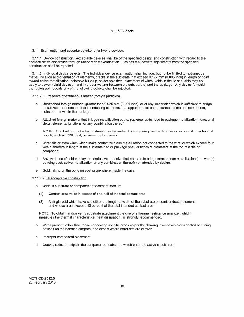
MIL-STD-883H
METHOD 2012.8 26 February 2010
10
3.11 Examination and acceptance criteria for hybrid devices.
3.11.1 Device construction. Acceptable devices shall be of the specified design and construction with regard to the characteristics discernible through radiographic examination. Devices that deviate significantly from the specified construction shall be rejected.
3.11.2 Individual device defects. The individual device examination shall include, but not be limited to, extraneous matter, location and orientation of elements, cracks in the substrate that exceed 0.127 mm (0.005 inch) in length or point toward active metallization, adhesive build-up, solder splashes, placement of wires, voids in the lid seal (this may not apply to power hybrid devices), and improper wetting between the substrate(s) and the package. Any device for which the radiograph reveals any of the following defects shall be rejected:
3.11.2.1 Presence of extraneous matter (foreign particles).
a. Unattached foreign material greater than 0.025 mm (0.001 inch), or of any lesser size which is sufficient to bridge metallization or nonconnected conducting elements, that appears to be on the surface of the die, component, substrate, or within the package.
b. Attached foreign material that bridges metallization paths, package leads, lead to package metallization, functional
circuit elements, junctions, or any combination thereof.
NOTE: Attached or unattached material may be verified by comparing two identical views with a mild mechanical shock, such as PIND test, between the two views.
c. Wire tails or extra wires which make contact with any metallization not connected to the wire, or which exceed four
wire diameters in length at the substrate pad or package post, or two wire diameters at the top of a die or component.
d. Any evidence of solder, alloy, or conductive adhesive that appears to bridge noncommon metallization (i.e., wire(s),
bonding post, active metallization or any combination thereof) not intended by design.
e. Gold flaking on the bonding post or anywhere inside the case.
3.11.2.2 Unacceptable construction.
a. voids in substrate or component attachment medium.
(1) Contact area voids in excess of one-half of the total contact area.
(2) A single void which traverses either the length or width of the substrate or semiconductor element and whose area exceeds 10 percent of the total intended contact area.
NOTE: To obtain, and/or verify substrate attachment the use of a thermal resistance analyzer, which measures the thermal characteristics (heat dissipation), is strongly recommended.
b. Wires present, other than those connecting specific areas as per the drawing, except wires designated as tuning
devices on the bonding diagram, and except where bond-offs are allowed.
c. Improper component placement.
d. Cracks, splits, or chips in the component or substrate which enter the active circuit area.
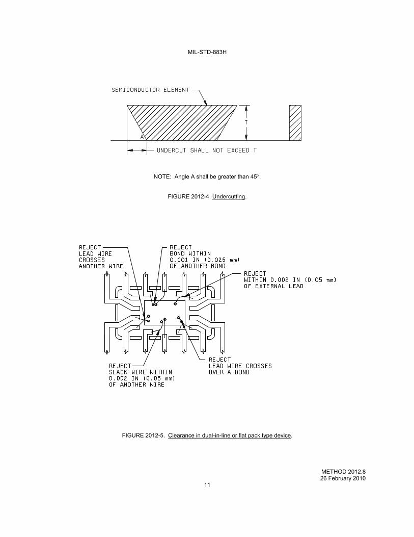
MIL-STD-883H
METHOD 2012.8 26 February 2010
11
NOTE: Angle A shall be greater than 45.
FIGURE 2012-4 Undercutting.
FIGURE 2012-5. Clearance in dual-in-line or flat pack type device.
MIL-STD-883H
METHOD 2012.8 26 February 2010
12
e. Voids in the lid seal in which the seal is not continuous or is reduced from its design sealing width by more than 75 percent.
NOTE: Sealing voids may not be detectable within power hybrid packages.
f. Inadequate clearance.
(1) Any wire that comes closer than 0.025 mm (0.001 inch) to another wire (excluding common wires) within a spherical radial distance from the bond perimeter of 0.127 mm (0.005 inch) for ball bonds, or 0.254 mm (0.010 inch) for ultrasonic and thermocompression wedge bonds.
NOTE: Insulated wires defined in the device specification/drawing are excluded from this criteria.
(2) Excessive loop or sag in any wire so that it comes closer than two wire diameters to another wire, package post, unglassivated operating metallization, die, or portion of a package after a spherical radial distance from the bond perimeter of 0.127 mm (0.005 inch) for ball bonds or 0.254 mm (0.010 inch) for ultrasonic and thermocompression wedge bonds.
NOTE: Insulated wires defined in the device specification/drawing are excluded from this criteria.
(3) Missing or extra wire(s) or ribbon(s) not in conformance with the bonding diagram except those wire(s) or ribbon(s) designated as microwave tuning devices on the bonding diagram.
NOTE: Extra wires added for statistical process control lot or lot sample bond strength/process machine/operator evaluation in accordance with MIL-PRF-38534 are excluded from this criteria.
(4) Any wire that has no arc and makes a straight line run from die bonding pad to package post.
(5) Wires crossing wires except common conductors or as allowed in 3.2.2e of method 2010
(condition A).
(6) Excessive height in any component or wire loop such that it is closer than 0.127 mm (0.005 inch) to the lid when installed.
(7) Any wires which are broken. NOTE: Wire bond tails, as defined by method 2017, are excluded from this criteria.
(8) Excessive sag where the wire lies on the substrate for a distance greater than 1/2 the distance
between the edge of the substrate bonding pad and the chip to which the wire is bonded, or comes closer than 0.025 mm (0.001 inch) to runout of any conductive epoxy which mounts the chip.
(9) Bonds placed so that the wire exiting from the bond crosses over another bond, except for common
bonds. NOTE: For RF/microwave devices, bonds placed so that the wire exiting from a bond crosses over
another bond, except by design, in which case the clearance shall be two wire diameters minimum (common bonds are excluded from this criteria).
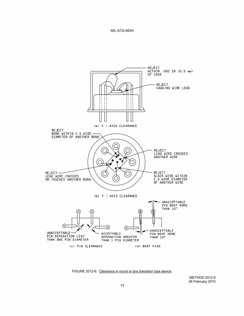
MIL-STD-883H
METHOD 2012.8 26 February 2010
13
FIGURE 2012-6. Clearance in round or box transistor type device.
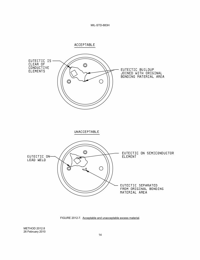
MIL-STD-883H
METHOD 2012.8 26 February 2010
14
FIGURE 2012-7. Acceptable and unacceptable excess material.
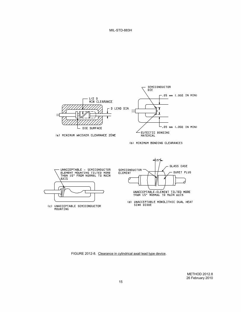
MIL-STD-883H
METHOD 2012.8 26 February 2010
15
FIGURE 2012-8. Clearance in cylindrical axail lead type device.
MIL-STD-883H
METHOD 2012.8 26 February 2010
16
4. Summary. The following details shall be specified in the applicable acquisition document:
a. Number of views, if other than indicated in 3.1.1. b. Radiograph submission, if applicable (see 3.9.2).
c. Marking, if other than indicated in 3.3 and marking of samples to indicate they have been radiographed, if required
(see 3.3.3).
d. Defects to be sought in the samples and criteria for acceptance or rejection, if other than indicated in 3.10.
e. Radiograph and report retention, if applicable (see 3.9.3).
f. Test reports when required for class level B.
MIL-STD-883H
METHOD 2013.1 16 May 1979
1
METHOD 2013.1
INTERNAL VISUAL INSPECTION FOR DPA
1. PURPOSE. This is an internal visual inspection for use in destructive physical analysis (DPA) procedures. The purpose of this destructive test is to examine devices opened for post test evaluation to verify that there is no evidence of defects or damage resulting from prior testing.
2. APPARATUS. The apparatus required for the performance of this test shall include binocular normal-incident illumination microscopes capable of 30X to 60X and 75X to 150X magnification with both light and dark field illumination, and any visual or mechanical standards to be used for measurements or comparison.
3. PROCEDURE. The device shall be opened using a technique which does not damage or contaminate the internal structure or in any way impair the ability to observe defects in the devices or the effects of preceding test exposures. The device(s) shall be examined microscopically at 30X to 60X for particles other than those produced by opening. After examination for particles is complete, the opened device(s) shall be blown off with a nominal gas blow (approximately 20 psig) to remove unattached material from the delidding process. The device shall then be microscopically examined to determine the existence of other visual defects as described in 3.1 and 3.2.
3.1 Low magnification defects (30X to 60X). No device shall be acceptable that exhibits the following defects:
a. Improper substrate or bonding post plating material.
b. Improper bond wire material or size. c. Metallic contamination or foreign material (see method 2010).
d. Lifted or broken wires.
e. Lifted, cracked, or broken die/substrate.
f. Improper die mounting (see method 2010).
g. Excessive lead wire loop or sag (see method 2010).
h. Improper bond technique and size (see method 2010).
i. Improper assembly die location and orientation as compared to the applicable assembly drawing.
j. Particles (see method 2010) other than those introduced during opening.
3.2 High magnification defects (75X to 150X). No device shall be acceptable that exhibits the following defects:
a. Metallization voids, corrosion, peeling, lifting, blistering, or scratches (see method 2010).
b. Bond intermetallics extending radially more than 0.1 mil beyond the bond periphery in any direction.
c. Improper die or substrate metallization design layout topography or identification.
d. Die cracks (see method 2010).
MIL-STD-883H
METHOD 2013.1 16 May 1979
2
4. SUMMARY. The following details shall be specified in the applicable acquisition document:
a. Where applicable, gauges, drawings, or photographs to be used as standards for the operator comparison (see 2).
b. Any applicable requirements for materials, design, or construction.
c. Requirement for photographic record, if applicable, and disposition of the photographs.
d. Where applicable, any additions or modifications to the specified procedure and criteria.
MIL-STD-883H
METHOD 2014 15 November 1974
1
METHOD 2014
INTERNAL VISUAL AND MECHANICAL
1. PURPOSE. The purpose of this examination is to verify that internal materials, design and construction are in accordance with the applicable acquisition document. This test is destructive and would normally be employed on a sampling basis in qualification or quality conformance inspection of a specific device type to demonstrate compliance with the acquisition document and to reveal any undocumented changes to the part type.
2. APPARATUS. Equipment used in this examination shall be capable of demonstrating conformance to the requirements of the applicable acquisition document and shall include optical equipment capable of magnification sufficient to verify all structural features of the devices.
3. PROCEDURE. The device shall be examined under a sufficient magnification to verify that all the internal materials, design and construction are in accordance with the requirements of the applicable design documentation or other specific requirements (see 4). Specimens of constructions which do not contain an internal cavity (e.g., encapsulated or embedded devices) or those which would experience destruction of internal features of interest as a result of opening, may be obtained by interception during manufacturing prior to encapsulation. Specimens of constructions with an internal cavity shall be selected from devices which have completed all manufacturing operations and they shall be delidded or opened or both taking care to minimize damage to the areas to be inspected. When specified by the applicable acquisition document, the interception procedure may be used to obtain specimens of constructions with an internal cavity.
3.1 Photographs of die topography and intraconnection pattern. When specified, an enlarged color photograph or transparency shall be made showing the topography of elements formed on the die or substrate and the metallization pattern. This photograph shall be at a minimum magnification of 80X except that if this results in a photograph larger than 8 inches x 10 inches, the magnification may be reduced to accommodate an 8 inches x 10 inches view.
3.2 Failure criteria. Devices which fail to meet the detailed requirements for materials, design and construction shall constitute a failure.
4. SUMMARY. The following details shall be specified in the applicable acquisition document:
a. Any applicable requirements for materials, design and construction.
b. Allowance for interception procedure of internal cavity devices, when applicable (see 3). c. Requirement for photographic record, if applicable (see 3.1), and disposition of photographs.
MIL-STD-883H
METHOD 2014 15 November 1974
2
This page intentionally left blank
MIL-STD-883H
METHOD 2015.13 18 December 2000
1
METHOD 2015.13 RESISTANCE TO SOLVENTS
1. PURPOSE. The purpose of this test is to verify that the markings will not become illegible on the component parts when subjected to solvents. The solvents will not cause deleterious, mechanical or electrical damage, or deterioration of the materials or finishes.
1.1 Formulation of solvents. The formulation of solvents herein is considered typical and representative of the desired stringency as far as the usual coatings and markings are concerned. Many available solvents which could be used are either not sufficiently active, too stringent, or even dangerous to humans when in direct contact or when the fumes are inhaled.
1.2 Check for conflicts. When this test is referenced, care should be exercised to assure that conflicting requirements, as far as the properties of the specified finishes and markings are concerned, are not invoked.
2. MATERIALS.
2.1 Solvent solutions. The solvent solutions used in this test shall consist of the following: 1/
a. At 20-30C a mixture consisting of the following:
(1) One part by volume of an aliphatic alcohol and/or aliphatic ester, USP grade or better.
(2) Three parts by volume of mineral spirits in accordance with A-A-2904, type II, previously designated as TT-T-291, type II, grade A, or three parts by volume of a mixture of 80 percent by volume of kerosene and 20 percent by volume of ethylbenzene.
b. A semiaqueous or nonaqueous based organic solvent e.g., a terpene or heterocyclic compound. 2/
c. This solvent has been deleted. When a suitable replacement for this solvent has been found, it will be added as
solution c.
d. At 63°C to 70°C, a mixture consisting of the following: 1/
(1) 42 parts by volume of deionized water.
(2) 1 part by volume of propylene glycol monomethyl ether.
(3) 1 part by volume of monoethanolamine or equivalent inorganic base to achieve the same pH.
2.1.1 Solvent solutions, safety aspects. Solvent solutions listed in a through d above exhibit some potential for health and safety hazards. The following safety precautions should be observed:
a. Avoid contact with eyes.
b. Avoid prolonged contact with skin.
c. Provide adequate ventilation.
d. Avoid open flame.
e. Avoid contact with very hot surfaces. 1/ Normal safety precautions for handling these solutions (e.g., same as those for diluted ammonium hydroxide) based
on O.S.H.A rules for Monoethanolamine or other precautionary measures with regard to flash point, toxicity, etc.
2/ Or any EPA demonstrated equivalent. When using EPA approved alternative solutions for test, the device manufacturer should consider the recommended temperature for cleaning specified by the solvent supplier.
MIL-STD-883H
METHOD 2015.13 18 December 2000
2
2.2 Vessel. The vessel shall be a container made of inert material, and of sufficient size to permit complete immersion of
the specimens in the solvent solutions specified in 2.1.
2.3 Brush. The brush shall be a toothbrush with a handle made of a nonreactive material. The brush shall have at least three long rows of hard (or firm) bristles, the free ends of which shall lie substantially in the same plane. The toothbrush shall be used exclusively with a single solvent and when there is any evidence of softening, bending, wear, or loss of bristles, it shall be discarded.
3. PROCEDURE. The specimens subjected to this test shall be divided into three equal groups. Each group shall be individually subjected to one of the following procedures:
Note: Metal lidded leadless chip carrier (LCC) packages shall be preconditioned by immersing the specimens in room temperature flux type symbols “A” or “B” (flux types “LO” or “L1”) in accordance with ANSI/J-STD-004 previously designated as RMA flux in accordance with MIL-F-14256, for 5 to 10 seconds. The specimens shall then be subjected to an ambient temperature of 215 °C 5°C for 60 seconds +5, -0 seconds. After the preconditioning, each device lid shall be cleaned with isopropyl alcohol.
a. The first group shall be subjected to the solvent solution as specified in 2.1a maintained at a temperature of 25°C
5°C.
b. The second group shall be subjected to the solvent solution as specified in 2.1b maintained at a suitable temperature.
c. This solution has been deleted, (see 2.1c).
d. The fourth group shall be subjected to the solvent solution as specified in 2.1d maintained at a temperature of 63°C
to 70°C. The specimens and the bristle portion of the brush shall be completely immersed for 1 minute minimum in the specified solution contained in the vessel specified in 2.2. Immediately following emersion, the specimen shall be brushed with normal hand pressure (approximately 2 to 3 ounces) for 10 strokes on the portion of the specimen where marking has been applied, with the brush specified in 2.3. Immediately after brushing, the above procedure shall be repeated two additional times, for a total of three immersions followed by brushings. The brush stroke shall be directed in a forward direction, across the surface of the specimen being tested. After completion of the third immersion and brushing, devices shall be rinsed and all surfaces air blown dry. After 5 minutes, the specimens shall be examined to determine the extent, if any, of deterioration that was incurred.
3.1 Optional procedure for the fourth group. The test specimens shall be located on a test surface of known area which is located 15 2.5 centimeters (6 ±1 inches) below a spray nozzle(s) which discharges 0.6 ±0.02 liters/minute (0.139 gpm) of solution (2.1d) per 6.5 square centimeters (1 in2)surface area at a pressure of 140 ±30 kilopascal (20 ±5 psi). The specimens shall be subjected to this spray for a period of 10 minutes minimum. After removal and within 5 minutes the specimens shall be examined in accordance with 3.1.1. The specimens may be rinsed with clear water and air blow dried prior to examination.
3.1.1 Failure criteria. After subjection to the test, evidence of damage to the device and any specified markings which are missing in whole or in part, faded, smeared, blurred, or shifted (dislodged) to the extent that they cannot be readily identified from a distance of at least 15.0 cm (6 inches) with normal room lighting and without the aid of magnification or with a viewer having a magnification no greater than 3X shall constitute a failure.
4. SUMMARY. The following detail shall be specified in the individual specification: The number of specimens to be tested (see 3).
MIL-STD-883H
METHOD 2016 15 November 1974
1
METHOD 2016
PHYSICAL DIMENSIONS
1. PURPOSE. The purpose of this examination is to verify that the external physical dimensions of the device are in accordance with the applicable acquisition document.
2. APPARATUS. Equipment used in this examination shall include micrometers, calipers, gauges, contour projectors, or other measuring equipment capable of determining the actual device dimensions specified in the applicable acquisition document.
3. PROCEDURE. Unless otherwise specified, the physical dimensions on the case outline drawing shall be measured.
3.1 Failure criteria. Any device which exhibits a dimension or dimensions outside the specified tolerances or limits shall constitute a failure.
4. SUMMARY. The following detail shall be specified in the applicable acquisition document:
External dimensions which are capable of physically describing the device (see 3). Dimensions to be considered shall include case outline dimensions; special lead shapes (e.g., required bend positions, angles of bend), where applicable; dimensions of any projecting or indented features used for coding of lead arrangement, automatic handling and similar purpose; and any other information which affects the installed size or orientation of the device in normal applications.
MIL-STD-883H
METHOD 2016 15 November 1974
2
This page intentionally left blank
MIL-STD-883H
METHOD 2017.9 26 February 2010
1
METHOD 2017.9
INTERNAL VISUAL (HYBRID) 1. PURPOSE. The purpose of this test is to visually inspect the internal materials, construction, and workmanship of hybrid, multichip and multichip module microcircuits.
1.1 SCOPE. This test is for both Class H (Class level B) and Class K (Class level S) quality levels, SAW and hybrid/multichip/multichip module microcircuits. The following types of microcircuits may be inspected:
a. Passive thin and thick film networks.
b. Active thin and thick film circuits.
c. Multiple circuits, including combinations, stacking or other interconnections of 1.1.a and 1.1.b. This test will normally be used on microelectronic devices prior to capping or encapsulation on a 100 percent inspection basis to detect and eliminate devices with internal defects that could lead to device failure in normal application. It may also be employed on a sampling basis prior to capping to determine the effectiveness of the manufacturers quality control and handling procedures. 2. APPARATUS. The apparatus for this test shall include optical equipment capable of the specified magnification(s) and visual standards/aids (gages, drawings, photographs, etc.) necessary to perform an effective examination and enable the operator to make objective decisions as to the acceptability of the device being examined. Adequate fixturing shall be provided for handling devices during examination to promote efficient operation without inflicting damage to the units. 3. PROCEDURE. a. General. The device shall be examined in a suitable sequence of observations within the specified magnification
range to determine compliance with the specified test condition. b. Sequence of inspection. The order in which criteria are presented is not a required order of examination and may
be varied at the discretion of the manufacturer. Where obscuring mounting techniques (e.g., beam lead devices, stacked substrates, components mounting in holes or cutaways, flip chip devices, packaged devices) are employed, the inspection criteria contained herein that cannot be performed after mounting shall be conducted prior to mounting the element or substrate. The inspection criteria of 3.1.1 may be performed at the option of the manufacturer prior to element attachment.
c. Inspection control. In all cases, examination prior to final preseal inspection shall be performed under the same
quality program that is required at the final preseal inspection station. Care shall be exercised after inspections (see 3.b), to ensure that defects created during subsequent handling will be detected and rejected at final preseal inspection. Devices examined to 3.1 criteria shall be inspected and prepared for sealing in a 100,000 (0.5 µm or greater) particles/cubic foot controlled environment (class 8 of ISO 14644-1) for Class H (Class level B) and 100 (0.5 µm or greater) particles/cubic foot controlled environment (class 5 of ISO 14644-1) for Class K (Class level S), except that the allowable relative humidity shall be less than 65 percent. During the time interval between internal visual inspection and preparation for sealing, devices shall be stored in a 1000 (0.5 µm or greater) particles/cubic foot controlled environment (class 6 of ISO 14644-1). Devices shall be in covered containers when transferred from one controlled environment to another.
d. Reinspection. When inspection for product acceptance or quality verification of the visual requirements herein is
conducted subsequent to the manufacturer's successful inspection, the additional inspection may be performed at any magnification specified by the applicable test condition, unless a specific magnification is required by the acquisition document. Where sample inspection is used rather than 100 percent reinpsection, the sampling plans of MIL-PRF-38534 or Appendix A of MIL-PRF-38535 shall apply.
*
*
*
*

MIL-STD-883H
METHOD 2017.9 26 February 2010
2
e. Exclusions. Where conditional exclusions have been allowed, specific instruction as to the location and conditions
for which the exclusion can be applied shall be documented in the assembly inspection drawing. f. Definitions.
(1) Active circuit area includes all areas of functional circuit elements, operating metallization or connected combinations thereof excluding beam leads.
(2) Add-on substrate is a supporting structural material into and/or upon which glassivation, metallization and
circuit elements are placed and the entire assembly is in turn placed on, and attached to the main substrate.
(3) Attachment media is defined as the material used to effect the attachment of an element to an underlying surface (e.g., adhesive, solder, alloy).
(4) Bonding site is a metallized area on a substrate or element intended for a wire or ribbon interconnecting bond.
(5) Cold solder joint is defined as a solder joint whose appearance is "grainy" or "dull". Where a "grainy" or "dull"
appearance is characteristic of certain solder materials (e.g., AuSn, etc.), this criteria shall not be rejectable for these materials.
(6) Compound bond is one bond on top of another.
(7) Conductive attach is the process and materials used for the attachment that also provides an electrical contact
or thermal dissipation path (e.g., solder, eutectic, solder-impregnated epoxy).
(8) Dielectric attach is the process and materials used for attachment that does not provide electrical contact or thermal dissipation considerations.
(9) Edge metallization is the metallization that electrically connects the metallization from the top surface to the
opposite side of the substrate; also called wrap around metallization.
(10) Element is a constituent of a hybrid microcircuit; such as integral deposited or screened passive elements, substrates, discrete or integrated electronic parts including dice, chips and other microcomponents; also mechanical piece parts as cases and covers; all contributing to the operation of a hybrid microcircuit.
(11) Electrically common is satisfied when two or more conductive surfaces or interconnects are of equal DC
voltage/signal potential.
(12) End terminated or wrap around elements are those elements which have electrical connections on the ends (sides) and/or bottom of their bodies.
(13) Foreign material is defined as any material that is foreign to the microcircuit or any non-foreign material that is
displaced from its original or intended position within the microcircuit package. Conductive foreign material is defined as any substance that appears opaque under those conditions of lighting and magnification used in routine visual inspection. Particles shall be considered embedded in glassivation when there is evidence of color fringing around the periphery of the particle.
(14) Glassivation is the top layer(s) of transparent insulating material that covers the active area including
metallization, except bonding pads and beam leads. Crazing is the presence of minute cracks in the glassivation.
*
MIL-STD-883H
METHOD 2017.9 26 February 2010
3
(15) Insulating layer is a dielectric layer used to isolate single or multilevel conductive and resistive material or to
protect top level conductive resistive material.
(16) Intermetallics (Purple Plague) is one of several gold-aluminum compounds formed when bonding gold to aluminum and activated by re-exposure to moisture and high temperature (>340C). Purple plague is purplish in color and is very brittle, potentially leading to time-based failure of the bonds. Its growth is highly enhanced by the presence of silicon to form ternary compounds.
(17) Mechanical strength tests are tests, such as Mechanical Shock or Constant Acceleration, which demonstrate
adequate attachment process and materials.
(18) Non-monometallic compound bond consists of two lead bonds, made of dissimilar metals, which are stacked one on top of the other (i.e., the interface between the two lead bonds are made up of dissimilar metals such as an aluminum lead bond stacked on top of a gold lead bond or vice-versa.
(19) Operating metallization (conductors) is all metal or any other material used for interconnections except
metallized scribe lines, test patterns, unconnected functional circuit elements, unused bonding pads and identification markings.
(20) Original design separation is the separation dimension or distance that is intended by design.
(21) Original width is the width dimension or distance that is intended by design (i.e., original metal width, original
diffusion width, original beam width, etc.).
(22) Passivation is the silicon oxide, nitride, or other insulating material that is grown or deposited directly on the die prior to the deposition of the final metal layers.
(23) String is a filamentary run-out or whisker of polymer material.
(24) Substrate is the supporting structural material into and/or upon which the passivation, metallization, and circuit
elements are placed.
(25) Tuning is the adjustment of signals from an RF/Microwave circuit by altering lines or pads; adding, deleting or manipulating wires/ribbons; and/or changing resistance, inductance or capacitance values to meet specific electrical specifications.
(26) Through hole metallization is the metallization that electrically connects the metallization on the top surface of
the substrate to the opposite surface of the substrate.
(27) Unused component or unused deposited element is one not connected to a circuit or connected to a circuit path at one and only one point. A connection may be made by design or by visual anomaly.
(28) Void is any region in the material (interconnects, bonding sites, etc.) where underlying material is visible that is
not caused by a scratch.
(29) Visible line is defined as 0.5 mil at 60X magnification.
g. Interpretations. References herein to "that exhibits" shall be considered satisfied when the visual image or visual appearance of the device under examination indicates a specific condition is present and shall not require confirmation by any other method of testing. When other methods of test are to be used to confirm that a reject condition does not exist, they shall be approved by the acquiring activity.
MIL-STD-883H
METHOD 2017.9 26 February 2010
4
h. Foreign material control. The manufacturer shall perform an audit on a weekly basis for the presence of foreign
material on the die surface, or within the package. This audit may be satisfied during routine internal visual inspection. If the presence of any type of foreign material/contamination is discovered, the manufacturer shall perform the necessary analysis on a sample of suspect devices to determine the nature of the foreign material. The manufacturer shall then document the results of his investigation and corrective actions to eliminate the foreign material and shall make this information available to the Government QAR, the acquiring activity, or the qualifying activity, as required. Corrective action responses shall be obtained within a maximum of ten (10) working days of discovery. The intent of this procedure is to require investigation and resolution of foreign material/contamination problems which do not have effective screening or detection methodology, but that could cause degradation and eventual failure of the device function. Repetitive findings without obvious improvements require escalation to Director of Manufacturing and Director of Quality Assurance, or their equivalents, to continue processing.
3.1 Examination. Internal visual examination as required in 3.1.1 through 3.1.9 shall be conducted on each SAW, hybrid/multichip microcircuit, or microwave hybrid microcircuit. The magnifications required for each inspection shall be those identified in the particular test method used (i.e., 2010, 2017, or 2032 of MIL-STD-883 and 2072, 2073 of MIL-STD-750). 3.1.1 Active and passive elements. All integrated circuit elements shall be examined in accordance with MIL-STD-883, method 2010. Class H Class K
(Class level B Monolithic) (Class level S Monolithic) Method 2010; Para. 3.1.1: Metallization defects. Method 2010; Para. 3.1.2: Diffusion and passivation layer(s) faults. Method 2010; Para. 3.1.3: Scribing and die defects. Method 2010; Para. 3.2.5: Foreign material. Method 2010; Para. 3.1.4: Glassivation defects. Method 2010; Para 3.1.6: Film resistors defects. Method 2010; Para. 3.1.7: Laser trimmed film resistor defects. Transistor and semiconductor diode elements shall be examined in accordance with MIL-STD-883, method 2010 (paragraphs referenced above) or the identified paragraphs of MIL-STD-750, methods 2072 and 2073 as indicated below. Passive elements (including substrates) shall be examined in accordance with MIL-STD-883, method 2032. Visual MIL-STD-750 MIL-STD-883 Inspection Method 2072 Method 2073 Method 2010 Die metallization 4.1.1 4.1.3, 4.1.5 3.1.1 defects Diffusion and 4.1.2 4.1.2 3.1.2 passivation layer(s) Scribing and die 4.1.3 4.1.1, 4.1.4 3.1.3 defects
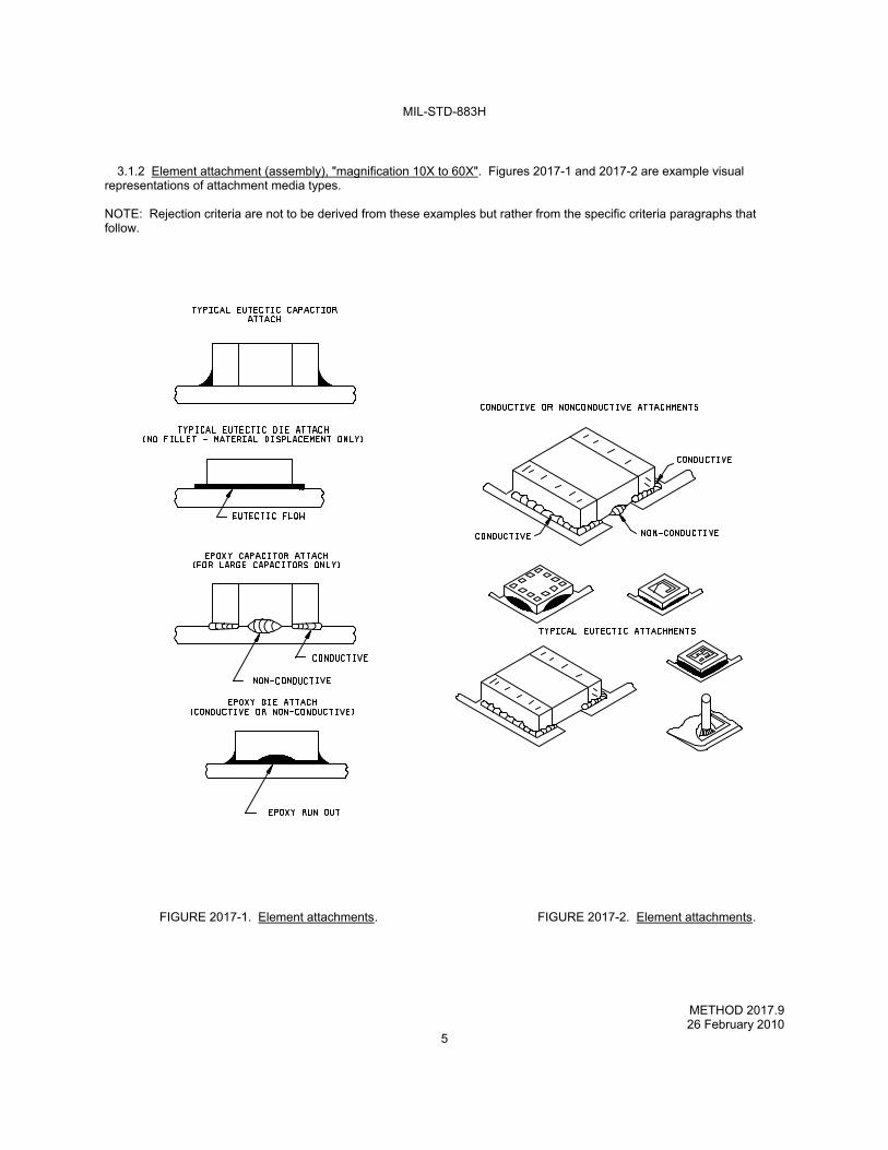
MIL-STD-883H
METHOD 2017.9 26 February 2010
5
3.1.2 Element attachment (assembly), "magnification 10X to 60X". Figures 2017-1 and 2017-2 are example visual representations of attachment media types. NOTE: Rejection criteria are not to be derived from these examples but rather from the specific criteria paragraphs that follow.
FIGURE 2017-1. Element attachments. FIGURE 2017-2. Element attachments.
MIL-STD-883H
METHOD 2017.9 26 February 2010
6
Class H Class K
Note: Mechanical strength or Dielectric attachment may be Radiography may be used to assessed through Mechanical Strength verify attachment in lieu of Testing. For conductive attachment, visual criteria. the Qualifying Activity may approve alternate methods for verifying attachment integrity.
No device shall be acceptable that exhibits: a. For non-end terminated elements, attachment media not visible around at least 50 percent of the perimeter unless
it is continuous on two full nonadjacent sides of the element. NOTE: The criteria of paragraph 3.1.2.a shall not apply when attachment material is applied directly to more than 50
percent of the element attach area by use of a method such as preforms or printing.
b. End terminated elements that do End terminated elements that do not not have conductive attachment have conductive attachment media media visible around at least visible around at least 75 percent 50 percent of the visible of the visible bonding pad perimeter bonding pad perimeter on each on each end termination. For end termination. For dielectric attachment of end dielectric attachment of end terminated elements (i.e., where terminated elements (i.e., the body of the element between the where the body of the element end terminations is attached), the between the end terminations is criteria of (a) above applies. attached), the criteria of (a) above applies.
c. Glass substrates or transparent die, when viewed from the bottom, which exhibit attach area less than 50 percent. NOTE: This criterion may be employed in lieu of 3.1.2.a. d. Flaking of the attachment media material. e. Balling of the solder or alloy material that does not exhibit a fillet. (see Figure 2017-3)

MIL-STD-883H
METHOD 2017.9 26 February 2010
7
FIGURE 2017-3. Balling of die attach material.
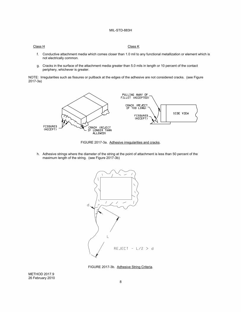
MIL-STD-883H
METHOD 2017.9 26 February 2010
8
Class H Class K f. Conductive attachment media which comes closer than 1.0 mil to any functional metallization or element which is
not electrically common. g. Cracks in the surface of the attachment media greater than 5.0 mils in length or 10 percent of the contact
periphery, whichever is greater. NOTE: Irregularities such as fissures or pullback at the edges of the adhesive are not considered cracks. (see Figure 2017-3a)
FIGURE 2017-3a. Adhesive irregularities and cracks. h. Adhesive strings where the diameter of the string at the point of attachment is less than 50 percent of the
maximum length of the string. (see Figure 2017-3b)
FIGURE 2017-3b. Adhesive String Criteria.
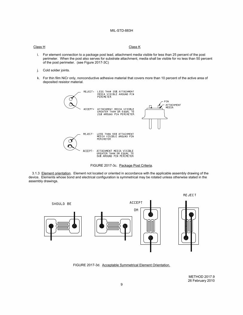
MIL-STD-883H
METHOD 2017.9 26 February 2010
9
Class H Class K i. For element connection to a package post lead, attachment media visible for less than 25 percent of the post
perimeter. When the post also serves for substrate attachment, media shall be visible for no less than 50 percent of the post perimeter. (see Figure 2017-3C)
j. Cold solder joints. k. For thin film NiCr only, nonconductive adhesive material that covers more than 10 percent of the active area of
deposited resistor material.
FIGURE 2017-3c. Package Post Criteria. 3.1.3 Element orientation. Element not located or oriented in accordance with the applicable assembly drawing of the device. Elements whose bond and electrical configuration is symmetrical may be rotated unless otherwise stated in the assembly drawings.
FIGURE 2017-3d. Acceptable Symmetrical Element Orientation.
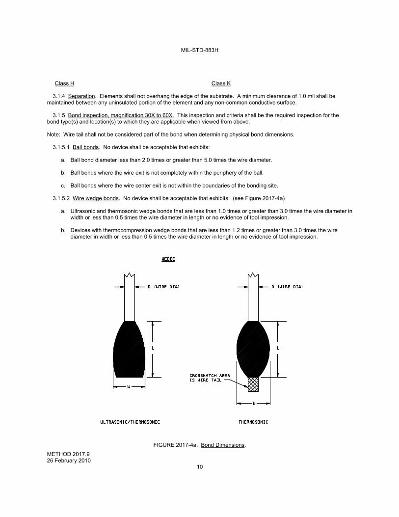
MIL-STD-883H
METHOD 2017.9 26 February 2010
10
Class H Class K 3.1.4 Separation. Elements shall not overhang the edge of the substrate. A minimum clearance of 1.0 mil shall be maintained between any uninsulated portion of the element and any non-common conductive surface. 3.1.5 Bond inspection, magnification 30X to 60X. This inspection and criteria shall be the required inspection for the bond type(s) and location(s) to which they are applicable when viewed from above. Note: Wire tail shall not be considered part of the bond when determining physical bond dimensions. 3.1.5.1 Ball bonds. No device shall be acceptable that exhibits: a. Ball bond diameter less than 2.0 times or greater than 5.0 times the wire diameter. b. Ball bonds where the wire exit is not completely within the periphery of the ball. c. Ball bonds where the wire center exit is not within the boundaries of the bonding site. 3.1.5.2 Wire wedge bonds. No device shall be acceptable that exhibits: (see Figure 2017-4a) a. Ultrasonic and thermosonic wedge bonds that are less than 1.0 times or greater than 3.0 times the wire diameter in
width or less than 0.5 times the wire diameter in length or no evidence of tool impression. b. Devices with thermocompression wedge bonds that are less than 1.2 times or greater than 3.0 times the wire
diameter in width or less than 0.5 times the wire diameter in length or no evidence of tool impression.
FIGURE 2017-4a. Bond Dimensions.
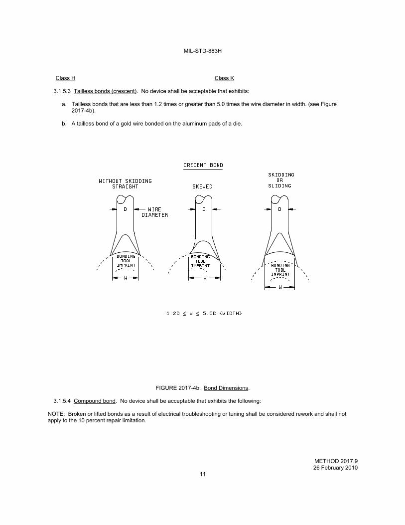
MIL-STD-883H
METHOD 2017.9 26 February 2010
11
Class H Class K 3.1.5.3 Tailless bonds (crescent). No device shall be acceptable that exhibits: a. Tailless bonds that are less than 1.2 times or greater than 5.0 times the wire diameter in width. (see Figure
2017-4b). b. A tailless bond of a gold wire bonded on the aluminum pads of a die.
FIGURE 2017-4b. Bond Dimensions. 3.1.5.4 Compound bond. No device shall be acceptable that exhibits the following: NOTE: Broken or lifted bonds as a result of electrical troubleshooting or tuning shall be considered rework and shall not apply to the 10 percent repair limitation.
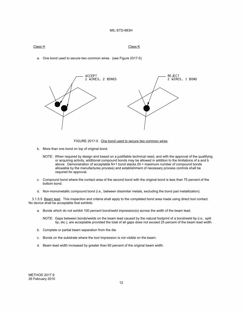
MIL-STD-883H
METHOD 2017.9 26 February 2010
12
Class H Class K a. One bond used to secure two common wires. (see Figure 2017-5)
FIGURE 2017-5. One bond used to secure two common wires. b. More than one bond on top of original bond.
NOTE: When required by design and based on a justifiable technical need, and with the approval of the qualifying or acquiring activity, additional compound bonds may be allowed in addition to the limitations of a and b above. Demonstration of acceptable N+1 bond stacks (N = maximum number of compound bonds allowable by the manufactures process) and establishment of necessary process controls shall be required for approval.
c. Compound bond where the contact area of the second bond with the original bond is less than 75 percent of the
bottom bond. d. Non-monometallic compound bond (i.e., between dissimilar metals, excluding the bond pad metallization). 3.1.5.5 Beam lead. This inspection and criteria shall apply to the completed bond area made using direct tool contact. No device shall be acceptable that exhibits: a. Bonds which do not exhibit 100 percent bond/weld impression(s) across the width of the beam lead.
NOTE: Gaps between bonds/welds on the beam lead caused by the natural footprint of a bond/weld tip (i.e., split tip, etc.), are acceptable provided the total of all gaps does not exceed 25 percent of the beam lead width.
b. Complete or partial beam separation from the die. c. Bonds on the substrate where the tool impression is not visible on the beam. d. Beam lead width increased by greater than 60 percent of the original beam width.
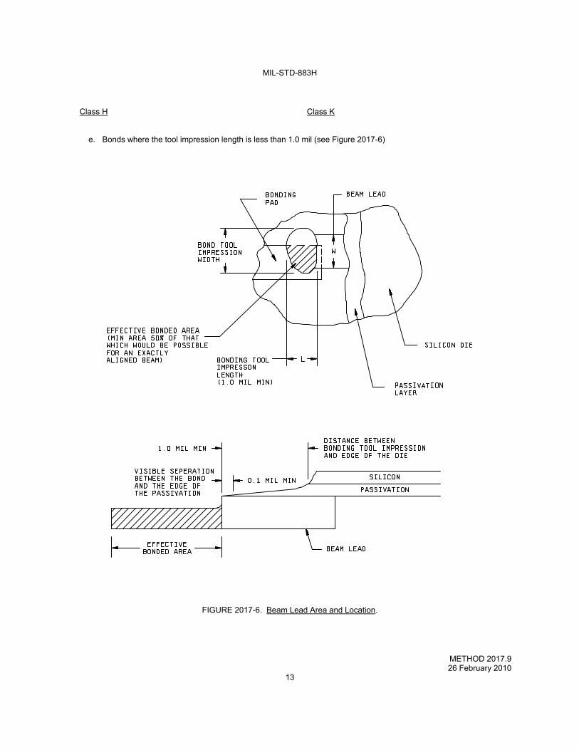
MIL-STD-883H
METHOD 2017.9 26 February 2010
13
Class H Class K e. Bonds where the tool impression length is less than 1.0 mil (see Figure 2017-6)
FIGURE 2017-6. Beam Lead Area and Location.
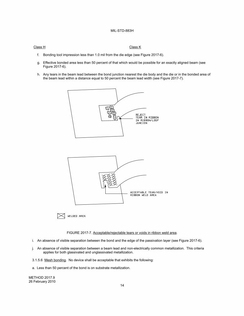
MIL-STD-883H
METHOD 2017.9 26 February 2010
14
Class H Class K f. Bonding tool impression less than 1.0 mil from the die edge (see Figure 2017-6). g. Effective bonded area less than 50 percent of that which would be possible for an exactly aligned beam (see
Figure 2017-6). h. Any tears in the beam lead between the bond junction nearest the die body and the die or in the bonded area of
the beam lead within a distance equal to 50 percent the beam lead width (see Figure 2017-7).
FIGURE 2017-7. Acceptable/rejectable tears or voids in ribbon weld area. i. An absence of visible separation between the bond and the edge of the passivation layer (see Figure 2017-6). j. An absence of visible separation between a beam lead and non-electrically common metallization. This criteria
applies for both glassivated and unglassivated metallization. 3.1.5.6 Mesh bonding. No device shall be acceptable that exhibits the following: a. Less than 50 percent of the bond is on substrate metallization.
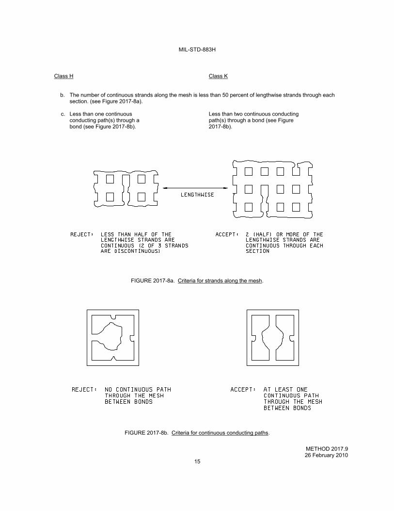
MIL-STD-883H
METHOD 2017.9 26 February 2010
15
Class H Class K b. The number of continuous strands along the mesh is less than 50 percent of lengthwise strands through each
section. (see Figure 2017-8a).
c. Less than one continuous Less than two continuous conducting conducting path(s) through a path(s) through a bond (see Figure bond (see Figure 2017-8b). 2017-8b).
FIGURE 2017-8a. Criteria for strands along the mesh.
FIGURE 2017-8b. Criteria for continuous conducting paths.
MIL-STD-883H
METHOD 2017.9 26 February 2010
16
Class H Class K 3.1.5.7 Ribbon bonds. No device shall be acceptable that exhibits the following: a. Any tears in the ribbon at the junction between the ribbon loop and bond/weld. b. Bonds which do not exhibit 100 percent bond/weld impression(s) across the width of the ribbon overlapping
underlying metallization. NOTE: Gaps between welds on the ribbon caused by the natural footprint of a weld tip (i.e., split tip, etc.) are acceptable provided the total of all gaps do not exceed 25 percent of the ribbon width. c. Effective bonded area less than 50 percent of that which would be possible for an exactly aligned ribbon. d. Bond tails longer than one ribbon width or 10.0 mils, whichever is less, or bridging adjacent metallization. e. The unbonded end of a ribbon bond tuning stub longer than one ribbon width of 10.0 mils, whichever is less, that is
not secured by polymer adhesive. 3.1.5.8 General. No device shall be acceptable that exhibits:
a. Bonds on the die where less a. Monometallic bonds on the die where less than 50 percent of the bond than 50 percent of the bond is within is within the unglassivated the unglassivated bonding site. bonding site. Bimetallic bonds on the die where less than 75 percent of the bond is within the unglassivated bonding site. b. Any metal that is displaced, as a result of b. Any metal that is displaced, as a result of bonding from its original position on the bonding from its original position on the bonding pad (shooting metal) that reduces the bonding pad (shooting metal) greater than 1.0 mils separation between unglassivated operation or that reduces the separation between metallization or scribe line to less than 0.25 mils unglassivated operation metallization or or 50 percent design separation, whichever scribe line to less than 0.25 mils or 50 percent is less. design separation, whichever is less. c. Bonds on the package post or substrate that are not completely within the bonding site.
NOTE: For cases where the substrate bonding site is smaller than 1.5 times the minimum bond size, bonds on the substrate where less than 50 percent of the bond is within the bonding site. d. Bonds placed so that the wire exiting from a bond crosses over another bond, except by design, in which case the
clearance shall be 2.0 wire diameters minimum (common bonds are excluded from this criteria). e. An absence of a visible line of separation between non-electrically common bonds. f. An absence of a visible line of separation between a bond and non-electrically common metallization. This criteria
applies to both glassivated and unglassivated metallization. g. Wire bond tails that extend over or make contact with any noncommon, unglassivated active metal.
h. Wire bond tails that exceed two wire diameters in length at the bonding pad or four wire diameters in length at the
package post. i. Bonds on element attach media or on contaminated or foreign material.
*

MIL-STD-883H
METHOD 2017.9 26 February 2010
17
Class H Class K j. Any lifted or peeling bond.
k. Intermetallic formation extending completely around the metallic interface of any bond between dissimilar metals. l. Wedge, crescent or ball bonds at the point where metallization exits from the bonding pad that do not exhibit a line of undisturbed metal visible between the periphery of the bond and at least one side of the entering metallization stripe. NOTE: Criteria of 3.1.5.8 (l) can be excluded when the entering conductor is >2 mils in width and the bond pad dimension on the entering conductor side is >3.5 mils. NOTE: For Class H only, the requirements for a visual line of metal can be satisfied when an acceptable wire tail obscures the area of concern, provided the following condition exists. Bond is located more than 0.1 mil from the intersecting line of the entering metallization stripe and the bonding pad and there is no visual evidence of disturbed pad metallization at the bond and wire tail interface. NOTE: Criteria 3.1.5.8 (l) is not applicable to interdigitated (Lange) couplers or when the interface between a thermosonic/ultrasonic (i.e., non-thermocompression) bond and underlying metal is monometallic. l. Polymeric adhesive which may be material or residue as evidenced by discoloration within 5.0 mils of the outer
periphery of a wire bond. m. Tearing at the junction of the wire and bond. The junction is the line of deformation of the wire at the bonding site. 3.1.6 Internal leads (e.g., wires, ribbons, beams, wireloops, ribbon loops, beams, etc.), "magnification 10X to 60X". No device shall be acceptable that exhibits: a. Within the first 5.0 mils of wire from the die surface for ball bonds, or 10.0 mils for wedge bonds, any wire that
comes closer than 1.0 mil to any non-common conductive surface (e.g., unglassivated operating metallization, unpassivated edge of conductive die).
NOTE: Insulated wires and electrically common wires are excluded from this criteria. b. After the first 5.0 mils of wire from the die surface for ball bond(s), or 10 mils for wedge bonds, any wire that comes
closer than two wire diameters to any non-common, uninsulated conductive surface (e.g., unglassivated operating metallization, unpassivated edge of conductive die).
NOTE: Insulated wires and electrically common wires are excluded from this criteria. c. Nicks, cuts, crimps, scoring, sharp bends, or neckdown in any lead that reduces the lead diameter/width by more
than 25 percent. d. Missing or extra lead(s) not in conformance with bonding diagram. NOTE: Leads designated for tuning on the bonding diagram are excluded. e. Any lead making a straight line run from bond to bond that has no arc, unless specifically allowed by the bonding
diagram. f. Wire(s) crossing wire(s) with a separation of less than 2 lead widths. Common or insulated conductors and
insulated wires are excluded. g. Complete or partial separation of the lead from the body of the element. h. Excessive loop height such that the wire would contact the lid when it is installed.
MIL-STD-883H
METHOD 2017.9 26 February 2010
18
Class H Class K 3.1.7 Screw tabs and through hole mounting, magnification 3X to 10X. No device shall be acceptable that exhibits: a. Misaligned tabs. b. Missing or broken tabs. c. Cracks emanating from mounting holes.
d. Loose substrates. e. Missing or loose screws. 3.1.8 Connector and feedthrough center contact soldering, magnification 10X to 30X. No device shall be acceptable that exhibits: a. Less than 50 percent of center contact overlaps onto metallized pattern (see Figure 2017-9). b. Center contact to substrate protrudes over onto circuit less than 1 diameter of a round pin or the width of a flat pin
(see Figure 2017-10).
c. Voids in solder (see Figure 2017-11a).
d. Cracked solder joint (see Figure 2017-11b). e. Poor adhesion of solder to center contact or substrate (see Figure 2017-11b). f. Insufficient or excess solder (see Figures 2017-11c through 2017-11e). g. Less than full coverage of solder along the length of the center contact and the metallization.
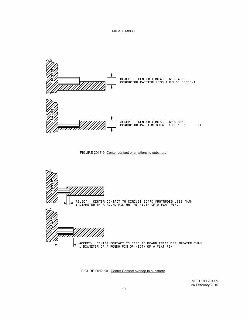
MIL-STD-883H
METHOD 2017.9 26 February 2010
19
FIGURE 2017-9 Center contact orientations to substrate.
FIGURE 2017-10. Center Contact overlap to substrate.
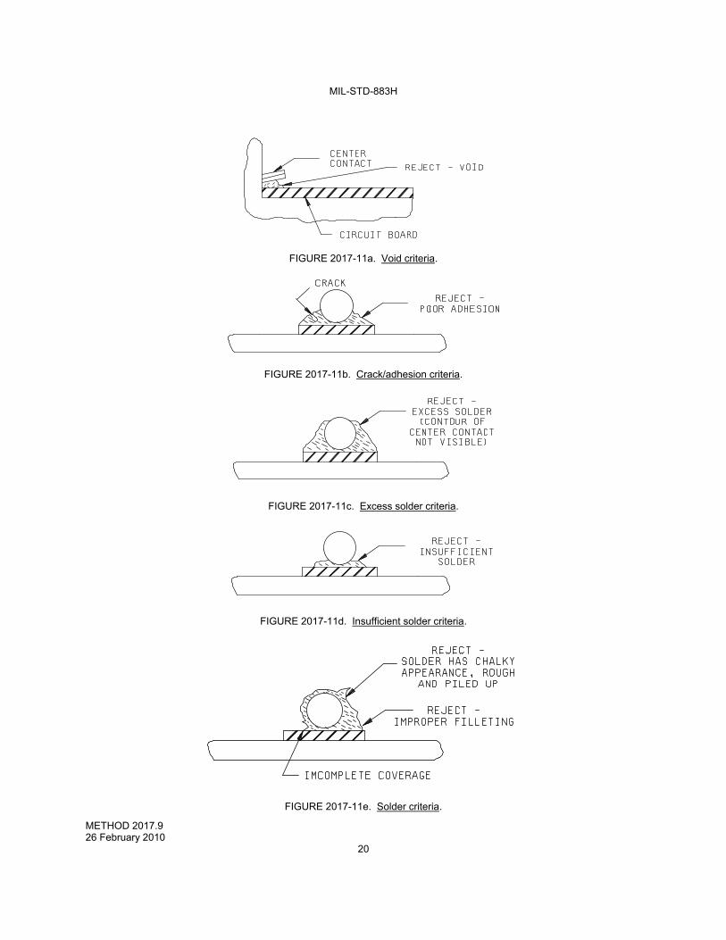
MIL-STD-883H
METHOD 2017.9 26 February 2010
20
FIGURE 2017-11a. Void criteria.
FIGURE 2017-11b. Crack/adhesion criteria.
FIGURE 2017-11c. Excess solder criteria.
FIGURE 2017-11d. Insufficient solder criteria.
FIGURE 2017-11e. Solder criteria.
MIL-STD-883H
METHOD 2017.9 26 February 2010
21
Class H Class K 3.1.9 Package conditions, "magnification 10X to 60X". No device will be acceptable that exhibits: a. Unattached foreign material within the package or on the seal flange. NOTE: All foreign material shall be considered to be unattached unless otherwise verified to be attached. Verification of attachments of foreign material whose longest dimensions are greater than 75 percent of the closest unglassivated conductive spacing shall be accomplished by a light touch with an appropriate mechanical device (i.e., needle, probe, pick, etc.). Verification of attachments of smaller material can be satisfied by suitable cleaning process approved by the acquiring activity. All foreign material or particles may be verified as attached with a nominal gas blow (approximately 20 psig).
NOTE: Semiconductor chips shall be considered foreign particles.
b. Attached foreign material that bridges metallization paths, two package leads, lead to package metallization,
functional circuit elements, junctions, or any combination thereof.
c. Liquid droplets or any chemical stain that bridges any combination of unglassivated operating metallization. d. Physical damage or contamination (eutectic or polymer material) that prevents adequate sealing of the seal
surface. e. Presence of any residual flux.
NOTE: Use 10X to 15X magnification. f. Foreign material in melt that does not exhibit a fillet. 4. SUMMARY. The following details shall be specified in the applicable acquisition document: a. Test condition (see 3). b. Where applicable, gages, drawings and photographs that are to be used as standards for operator comparison
(see 2). c. Where applicable, specific magnification if other than that specified (see 3).

MIL-STD-883H
METHOD 2017.9 26 February 2010
22
This page intentionally left blank