microwave measurement on conductive carbon nanotubes
DESCRIPTION
Phd ThesisTRANSCRIPT

Simulation and Microwave Measurement of the
Conductivity of Carbon Nanotubes
By Daniel Ifesinachi Odili
A thesis submitted to the University of Birmingham for the degree of
DOCTOR OF PHILOSOPHY
The University of Birmingham
School of Electronic, Electrical and Computer Engineering
College of Engineering and Physical Sciences
December 2010

University of Birmingham Research Archive
e-theses repository This unpublished thesis/dissertation is copyright of the author and/or third parties. The intellectual property rights of the author or third parties in respect of this work are as defined by The Copyright Designs and Patents Act 1988 or as modified by any successor legislation. Any use made of information contained in this thesis/dissertation must be in accordance with that legislation and must be properly acknowledged. Further distribution or reproduction in any format is prohibited without the permission of the copyright holder.
i
BIOGRAPHICAL SKETCH
Daniel Odili attended Irwin College in Leicester, United Kingdom, graduating in 2003. He
completed his Bachelors of Science with Honours in Electronic and Electrical Engineering at
the University of Birmingham, United Kingdom, in July 2006. His undergraduate project was
on emerging devices simulation under the supervision of Dr Tony Childs. In this project, he
modelled electron transport in carbon nanotubes. Daniel continued his graduate programme at
the University of Birmingham in October, 2006. He stayed within the emerging device
technology group in the department of Electrical, Electronic and Computer Engineering. His
doctorate programme on simulation and microwave measurement of the conductivity of
carbon nanotubes was supervised by Dr Tony Childs. Daniel collaborated with the
microwave group at Cardiff University to undertake the microwave studies of carbon
nanotubes.

ii
ABSTRACT
Recently, excellent properties have been realised from structures formed by carbon
nanotubes. This propelled their use as nanoscale electronic devices in the information
technology industry. The discovery of carbon nanotubes has stimulated interest in carbon-
based electronics. Metal-Oxide-Semiconductor systems (MOS) are used to model charge
transport within these carbon structures. Schrodinger‟s equation is solved self-consistently
with Poisson‟s equation. The Poisson equation, which defines the potential distribution on the
surface of the nanotube, is computed using a two-dimensional finite difference algorithm
exploiting the azimuthal symmetry. A solution to the Schrodinger‟s equation is required to
obtain the wavefunctions within the nanotube model. This is implemented with the scattering
matrix method. The resulting wavefunctions defined on the nanotube surface are normalised
to the flux computed by the Landauer equation. A novel implementation of the Schrodinger-
Poisson solver for providing a solution to a three dimensional nanoscale system is described.
To avoid convergence problems, an adaptive Simpson‟s method is employed in the model
devices. Another main contribution to this field is the highlighting of the differences in the
output characteristics of carbon nanotube- and graphene-based devices. In addition, the
source and drain contacts that give an optimum device performance are identified. The
limitation of this model is that quantised conductance appears on making contact to the
nanotube ends. Electron transport in carbon nanotubes can be studied using non-contacting
means. A new approach is to induce current in the nanotubes using microwave energy. A
resonator-based measurement method is used to examine the electrical properties of the
nanotubes. Remarkably, the nanotubes appear to have the smallest sheet resistance of any
non-superconducting material. The possibility of a ferromagnetic carbon nanotube is
investigated due to the remarkable screening properties observed. Measurements of the
magnetisation as a function of the applied magnetic field are conducted using a vector
vibrating sample magnetometer. The morphology and microstructure of the nanotubes are
observed using scanning electron microscopy (SEM) and transmission electron microscopy
(TEM), respectively. Carbon nanotubes can be contaminated with metal particulates during
growth. These impurities can modify charge transport in these carbon structures.

iii
ACKNOWLEDGMENT
Firstly, I would like to thank God for giving me knowledge and wisdom. I would like to
appreciate my family for praying for me continually and supporting my education financially.
I would like to appreciate the efforts of Dr Tony Childs to see that I complete my PhD. He
was my personal tutor for my undergraduate programme and now my project supervisor for
my doctorate programme.
I would like to extend my appreciation to Professor Adrian Porch at Cardiff University for his
contribution to this project. I would like to acknowledge the contributions of my research
colleagues to this work, mostly Yudong Wu and Aslam Sulaimalebbe. I would like to extend
my appreciations to Dr P. Weston, one of my advisors throughout my stay in this department.
Finally, I would like to thank the department of electrical, electronic and computer
engineering for accommodating me for both my undergraduate and postgraduate
programmes.

iv
Table of Contents
Biographical Sketch
Abstract
Acknowledgement
List of Figures
List of Tables
List of Symbols
Chapter 1.............................................................................................................. 1
Introduction ...................................................................................................... 1
1.1 Carbon Structures ............................................................................................................. 1
1.2 Carbon Electronics ........................................................................................................... 3
1.3 Thesis Outline .................................................................................................................. 7
1.4 References ...................................................................................................................... 10
Chapter 2............................................................................................................ 14
Modelling Charge Transport in Carbon Nanotubes using a Coupled
Schrodinger-Poisson Solver .......................................................................... 14
2.1 Introduction .................................................................................................................... 14
2.1.1 Graphene .................................................................................................................. 15
2.1.2 Carbon Nanotubes .................................................................................................. 20
2.2 Modelling Techniques .................................................................................................... 27

v
2.2.1 Finite Difference Method ........................................................................................ 27
2.2.2 Scattering Matrix Method ........................................................................................ 32
2.3 A Two-Dimensional Simulation of Carbon Nanotube Field-Effect Transistors............ 35
2.4 Simulation Results.......................................................................................................... 42
2.4 Role of the Metal-Carbon Nanotube Contact in Computing Electron Transport in
Carbon Nanotubes ................................................................................................................ 47
2.5 Conclusions .................................................................................................................... 53
2.6 References ...................................................................................................................... 54
Chapter 3............................................................................................................ 57
Comparison of the Current-Voltage Characteristics of MOS Devices
Based on Carbon Nanotubes and Graphene ............................................... 57
3.1 Introduction .................................................................................................................... 57
3.2 Model - Graphene Nanostrip Field Effect Transistors (GFETs) .................................... 58
3.3 Device Simulation .......................................................................................................... 60
3.4 Simulation Results.......................................................................................................... 63
3.5 Conclusions .................................................................................................................... 69
3.6 References ...................................................................................................................... 70
Chapter 4............................................................................................................ 72
Experiment – Contactless Measurements of Electron Transport in
Carbon Nanotubes ......................................................................................... 72
4.1 Introduction - Metallic Contact Limitations .................................................................. 72
4.2 Experimental Techniques ............................................................................................... 74
4.2.1 Scanning Electron Microscopy/Transmission Electron Microscopy [5] ................. 74
4.2.2 Energy Dispersive X-ray Spectroscopy [7] ............................................................. 75

vi
4.3 Microstructure and Morphology of the CNTs................................................................ 76
4.4. Copper Hairpin Resonator ............................................................................................. 80
4.5 Experimental Analysis using Cavity Perturbation Technique ....................................... 83
4.6 Experimental Results...................................................................................................... 89
4.7 Conclusions .................................................................................................................... 95
4.8 References ...................................................................................................................... 96
Chapter 5............................................................................................................ 98
3D Electromagnetic Simulation of Hairpin Resonator for the Microwave
Characterisation of Carbon Nanotubes Sample ......................................... 98
5.1 Introduction .................................................................................................................... 98
5.2 Background .................................................................................................................... 99
5.2.1 Theory of COMSOL Multiphysics [4] .................................................................. 100
5.2.2 Skin Depth ............................................................................................................. 104
5.2.3 Calculation of the Charge Density in a Carbon Nanotube .................................... 105
5.3 Modelling of Hairpin Resonator .................................................................................. 109
5.3.1 Introduction ........................................................................................................... 109
5.3.2 Hairpin Resonator Model ...................................................................................... 112
5.3.3 Simulation Results ................................................................................................. 114
5.4 Discussion .................................................................................................................... 119
5.5 Conclusions .................................................................................................................. 122
5.6 References .................................................................................................................... 123
Chapter 6.......................................................................................................... 125
Conclusions and Future Work ................................................................... 125
6.1 General Observation ..................................................................................................... 125

vii
6.2 Future Outlook ............................................................................................................. 127
6.3 References .................................................................................................................... 129
Appendix 1 ..................................................................................................................... 130
Appendix 2 ..................................................................................................................... 134
Appendix 3 ..................................................................................................................... 137
Appendix 4 ..................................................................................................................... 139
Appendix 5 ..................................................................................................................... 144
Appendix 6 ..................................................................................................................... 147
Appendix 7 ..................................................................................................................... 148
Appendix 8 ..................................................................................................................... 151
Appendix 9 ..................................................................................................................... 162
Appendix 10 ................................................................................................................... 163
List of Appendices
A1. Detailed Procedure for Implementing a Finite Difference Algorithm ............................ 130
A2. Explanation of the Scattering Matrix Method by Analysing a Single Symmetric Planar
Barrier of Defined Width and Height .................................................................................... 134
A3. Derivation of the Laplace equation as a Function of Polar and Cylindrical Coordinates
................................................................................................................................................ 137
A4. A Detailed Procedure for Computing the Electrostatic Potential within the CNFET
Structure ................................................................................................................................. 139
A5. A Detailed Description of the Grid Implementation for the CNFET Device ................. 144
A6. Debye Length Theory ..................................................................................................... 147
A7. The Images Obtained from the Morphology and Microstructural Studies Conducted on
the Nanotube Sample ............................................................................................................. 148

viii
A8. 3D Electromagnetic Simulation of Sapphire Dielectric Resonator for the Microwave
Characterisation of Carbon Nanotubes Sample ..................................................................... 151
A9. Publication - Modelling Charge Transport in Graphene Nanoribbons and Carbon
Nanotubes using a Schrodinger–Poisson Solver.................................................................... 162
A10. Publication - Microwave Characterisation of Carbon Nanotube Powders ................... 163
List of Figures
Figure 1.1: Some allotropes of carbon [2]. ................................................................................ 2
Figure 2.1: Graphene Lattice. The carbon atoms are illustrated using the shaded nodes and the
chemical bonds represented by the lines are derived from the -orbitals. The primitive
lattice vectors are and the unit-cell is the shaded region. There are two carbon atoms per
unit-cell, represented by and . ............................................................................................. 16
Figure 2.2: The dispersion relation of graphene. The conduction and valence states meet at K-
points. ....................................................................................................................................... 20
Figure 2.3: (a) Hexagonal lattice structure of a graphene sheet, (b) carbon nanotube formed
by rolling up a graphene sheet [6][7]. ...................................................................................... 21
Figure 2.4: A zig-zag carbon nanotube, where represents the length of the unit cell. ......... 23
Figure 2.5: Brillouin zone for a zig-zag nanotube super-imposed on graphene -
space. The wave vectors along the nanotube axis and perpendicular direction are represented
by and , respectively. The dash lines at the ends are for zone boundaries and they count
as a single slice......................................................................................................................... 24
Figure 2.6: (a), (b) - Typical nodes in cylindrical coordinates and (c) Finite difference grid for
an axisymmetric system. .......................................................................................................... 28
Figure 2.7: Interface between two different media. ................................................................. 30
Figure 2.8: Flux of carriers injected from each contact into the device (a). A fraction of the
flux from both sides transmits across the device Equilibrium and Under bias. .......... 32

ix
Figure 2.9: Fluxes of charge carriers incident upon and reflected from a slab of finite
thickness. .................................................................................................................................. 33
Figure 2.10: Two scattering matrices cascaded to produce a single, composite scattering
matrix. ...................................................................................................................................... 34
Figure 2.11: The Coaxial Carbon Nanotube FET Geometry. .................................................. 35
Figure 2.12: Cylindrical Coordinates. ...................................................................................... 36
Figure 2.13: Iterative procedure for computing electrostatics and charge transport self-
consistently. ............................................................................................................................. 42
Figure 2.14: Simulation of the potential energy seen by the electrons at different gate bias for
the equilibrium condition ( . Conduction band edge along the length of the device
for , and . ..................................................................... 43
Figure 2.15: Conduction band edge along the device length for ,
and . The energies are with respect to the source Fermi level. ............................ 44
Figure 2.16: Simulation of the carrier density as a function of position and varying
when . ................................................................................................................... 44
Figure 2.17: Transmission probabilities for electrons (a), and the corresponding conduction
band edge (b) at and . ...................................................................... 45
Figure 2.18: The I-V characteristics of the zig-zag nanotube for different gate bias. ............. 46
Figure 2.19: Drain current characteristics for the nanotube based on the FETtoy model [15] 46
Figure 2.20: A carbon nanotube „end bonded‟ to the metal, a carbon nanotube
forming „side contacts‟ on gold electrodes .............................................................................. 48
Figure 2.21: The band bending for the metal/nanotube junction at ,
and the transmission probability for electrons at . [
with - (a), (b)], [ with - (c), (d)] and [ with - (e), (f)].
The band bending occurs over a length scale . .................................................................... 50
Figure 2.22: Plot of CNFETs I-V characteristics as a function of metal contacts at .
.................................................................................................................................................. 51
Figure 2.23: The ideal output characteristics of the device without contact effects [15]. ....... 52
Figure 3.1: Cubical geometry of Graphene FET. .................................................................... 59
Figure 3.2: Normalised potential updates after each iteration. ................................................ 63
Figure 3.3: Simulation of the potential energy seen by the electrons at (a) 3D
view of the conduction band edge at (b) 3D view of the conduction band edge at

x
(c) Conduction band edge along the length of the device for different at the
edge of the graphene sheet (d) Conduction band edge along the length of the device for
different at the centre of the graphene sheet. ................................................................... 64
Figure 3.4: Simulation of the carrier density at . (a) 3D view of the net carrier
density as a function of position at . (b) 3D view of the net carrier density as a
function of position at . (c) Cross-section of carrier density for different at
the centre of graphene sheet (d) Cross-section of carrier density for different at the edge
of the graphene sheet. .............................................................................................................. 65
Figure 3.5: I-V characteristics of Graphene (a) and CNT (b) .................................................. 66
Figure 3.6: Transmission Probability and Fermi Dirac Distribution for different . Carbon
nanotubes – (a), (c), (e) and graphene – (b), (d), (f) ................................................................ 68
Figure 4.1: (a) A small drain bias applied across the channel causing a splitting of the
electrochemical potentials. (b) Energy level broadening due to the process of coupling to the
channel. .................................................................................................................................... 73
Figure 4.2: SEM image of the CNTs used for this experiment (a) before and (b,c) after
manual grinding. ...................................................................................................................... 77
Figure 4.3: (a) The TEM image of the nanotube sample, the dark spots representing the
impurities and (b) an evidence of the Fe content (inset) in the STEM image of the sample. .. 78
Figure 4.4: EDX result showing the composition of the CNTs. .............................................. 79
Figure 4.5: A schematic of the hairpin resonator used for the microwave measurements [9].
(a) Side view (b) Top view and (c) Inner structure. ................................................................. 81
Figure 4.6: The spectral response of a resonator in transmission mode observed using the
Agilent E5071B Network Analyser. ....................................................................................... 82
Figure 4.7: (a) 3GHz copper hairpin resonator & (b) Inner structure of the resonator. ........... 83
Figure 4.8: Screening current in the CNTs sample due to applied magnetic field. ................. 84
Figure 4.9: Possible screening current patterns for various orientations of the CNTs in the
bulk sample. ............................................................................................................................. 85
Figure 4.10: One of the possible geometries of the nanotubes in the bulk sample.................. 86
Figure 4.11: Spectral response of the empty hairpin resonator. .............................................. 90
Figure 4.12: Calibration experiment: (a) Quartz tube loaded with copper spheres. (b) Spectral
response of the hairpin resonator when loaded with small copper spheres. ............................ 91

xi
Figure 4.13: (a) Spectral response of the hairpin resonator when loaded with nanotubes
sample, (b) Scaled plot of the spectral response shown in (a). ................................................ 92
Figure 4.14: Resonant traces for graphite powder. .................................................................. 93
Figure 4.15: Magnetisation versus applied magnetic field curve for the sample with a mass of
. ........................................................................................................................................ 94
Figure 5.1: Cylindrical geometry of (a) carbon nanotube, and (b) copper wire. ................... 105
Figure 5.2: The representation of the Fermi surface in momentum space [7]. ...................... 106
Figure 5.3: Density of states for a carbon nanotube calculated using Eq. 5.33. .......... 108
Figure 5.4: Schematics of the hairpin resonator, where is the plate length, is the plate
width, is the separation between the plates and is the plate thickness [9][11]. ............... 109
Figure 5.5: 3D geometry of the hairpin resonator modelled using COMSOL Multiphysics. 112
Figure 5.6: 3D geometry of the hairpin resonator cut in half to reduce the size of the RF
cavity problem. ...................................................................................................................... 113
Figure 5.7: Field concentration and distribution within the hairpin. (a) High magnetic field
concentration observed at the short-circuited end of the hairpin. (b) Electric field is maximum
at the open end of the hairpin. ................................................................................................ 115
Figure 5.8: Top view of the magnetic field pattern within the radiation shield of the hairpin
resonator. ................................................................................................................................ 115
Figure 5.9: The hairpin resonator is loaded with tightly packed nanotubes sample ( in
volume corresponding to a sample mass of ). ............................................................. 116
Figure 5.10: Quantization of electronic wave states around a carbon nanotube. (a) The
parallel and perpendicular axes of a CNT. (b) The contour plot of graphene valence states for
a CNT [13]. ............................................................................................................................ 120
Figure 5.11: Screening currents for the microwave magnetic field applied parallel to the
nanotube axis. ........................................................................................................................ 120
Figure A1.1: Common grid patterns: (a) rectangular grid, (b) skew grid, (c) triangular grid,
(d) circular grid. ..................................................................................................................... 130
Figure A1.2: Estimates for the derivative of at P using forward, backward, and central
differences. ............................................................................................................................. 131
Figure A1.3: Finite difference mesh for two independent variables and . ........................ 132

xii
Figure A2.1: A simple rectangular tunnelling barrier ............................................................ 134
Figure A3.1: Cylindrical Coordinates. ................................................................................... 137
Figure A5.1: Grid implementation of the azimuthal symmetry in the coaxial CNFET. ....... 144
Figure A7.1: (a), (b) - Series of TEM micrographs showing the microstructure of the CNTs.
(c), (d) - Images (a) and (b) are magnified, black spots showing impurities. ........................ 148
Figure A7.2: (a), (b) – Series of STEM photographs showing the bulk nanotube sample. ... 149
Figure A7.3: EDX analysis is performed on the inset shown in (a). (b) – Carbon, (c) –
Silicon, and (d) – Iron ............................................................................................................ 150
Figure A8.1: Field configuration for a resonant mode [3]. ....................................... 152
Figure A8.2: A schematic of the cylindrical sapphire resonator. (a) Resonator with the field
lines, dotted lines represent magnetic field patterns while the solid lines represent the electric
field patterns (b) Top view of the structure. .......................................................................... 153
Figure A8.3: 2D & 3D geometries of the sapphire resonator modelled using COMSOL. .... 156
Figure A8.4: The magnetic field pattern in the sapphire resonator simulated using
COMSOL (a) before inserting the conducting sample, (b) after inserting the sample. ......... 157
Figure A8.5: Field screening observed when the conducting sample is placed in the region of
high magnetic field. (a) Assumed conductivity of , and (b) conductivity of .
................................................................................................................................................ 159
Figure A8.6: The plot of the magnetic field strength against position along the
surface of the conducting sample with varying conductivity. ............................................... 160
List of Tables
Table 2.1: The bandstructure properties of the first three subbands, where is the
greatest common divisor of and [8]. ................................................................................... 26
Table 4.1: Elemental analysis of the nanotubes sample using EDX........................................ 79
Table 5.1: Recorded increase in the resonant frequency as the conductivity of the nanotubes
sample increases..................................................................................................................... 117
Table A8.1: The skin depth computed from our simulation model is compared to that of the
surface resistivity model. ....................................................................................................... 158

xiii
List of Symbols
- Atomic wavefunctions
– Hamiltonian operator
- Dispersion relation
- Chiral (wrapping) vector
– Nanotube radius
- Length of nanotube
– Transmission coefficients
– Wavevector
– Electric potential
– Charge density
- Relative permittivity
– Gate radius
- Insulator thickness
– Nanotube surface potential
- Wavefunction of carriers
– Energy
- Bandgap
- Effective mass

xiv
- Local effective potential
- Electron affinity of carbon nanotube
– Source voltage
– Drain voltage
– Gate voltage
- Work function
- Probability current
- Landauer current
- Fermi-Dirac carrier distribution
- Electron charge
- Free electron mass
- Drain current
- Debye length
- Relative permeability
- Speed of light
– Resonant frequency
- Load impedance
- Bandwidth at half-maximum power
- Applied magnetic field
- Current density
- Electrical conductivity
- Sheet resistance
- Skin depth
- Permeability of free space
- Permittivity of free space
- Quality factor
- Loss tangent

xv
- Velocity
- Electric flux density
- Magnetisation
- Polarisation density
- Loop potential
- Angular frequency
- Power loss in the sample
- Dielectric power loss
- Power loss due to fields radiation.
- Electron orbital magnetic moment
- Current
- Bohr magneton
- Planck‟s constant
– Boltzmann‟s constant

Chapter 1. Introduction
Page 1 of 179
Chapter 1
Introduction
1.1 Carbon Structures
Over the past several decades, the density of devices on a microprocessor has been doubling
every three years. Metal-oxide-semiconductor field-effect transistors (MOSFETs) are now
approaching their scaling limit. To avoid scaling issues the channel of a MOS device could be
replaced with a nanoscale structure. A carbon nanotube (CNT) can serve as the channel of a
MOS device because it is a nanoscale structure with excellent electronic properties.
In the early nineties, Sumio Iijima brought CNTs into the awareness of the scientific
community [1]. Since then, there has been rapid progress in understanding their electronic
properties. CNTs are cylindrical structures of nanometric size, based on a hexagonal lattice of
carbon atoms. Before the electronic properties of CNTs can be understood, the properties of
the carbon atom must first be studied.
There are six electrons inside a carbon atom, which orbit the nucleus in shells. Two electrons
are in the inner shell while the other four are in the outer shell. The state of these outer
electron shells determines the stability of the carbon atoms. A stable arrangement is achieved
when the outer electron shell is full. Atoms gain, lose, or share electrons with neighbouring
atoms so that all the atoms involved end up with complete outer shells. As they share
electrons in a reaction, they form bonds between each other, leading to molecules and
compounds formation.

Chapter 1. Introduction
Page 2 of 179
Fig. 1.1 shows different crystalline forms of carbon. These crystalline forms of carbon are
called allotropes, which include diamond, graphite, buckyball, graphene and carbon nanotube
[2].
Figure 1.1: Some allotropes of carbon [2].
Diamond is the hardest natural substance on earth due to the strong bonding between the
carbon atoms. Each carbon atom in a diamond molecule is joined to four others in a
tetrahedron structure. The bonds have similar strength and a regular pattern through the
molecule.
Graphite is a layered compound, the carbon atoms on each layer are arranged in a hexagonal
lattice with separation of and the distance between the planes is .
Fullerene is an allotrope of carbon with a structure similar to that of graphite but the carbon
atoms are linked in hexagonal and pentagonal patterns. The surface of a fullerene molecule
looks like a soccer ball, which gave it the name buckyball.

Chapter 1. Introduction
Page 3 of 179
Graphene is a flat monolayer of carbon atoms, tightly packed into a two-dimensional
honeycomb lattice [3]. It is the basic building block for graphitic materials of all other
dimensionalities. Initially, graphene was presumed not to exist in free state but Novoselov
et.al [3] managed to extract graphene from bulk graphite in 2004. Graphene has the potential
to be the building block for next generation nanoelectronics because of its unique electronic
properties.
CNT is the main allotrope of carbon studied in this work. CNTs are categorized as single-
walled nanotubes (SWNTs) and multi-walled nanotubes (MWNTs). A SWNT consists of a
single graphene sheet rolled up to form a tube while a MWNT consists of multiple graphene
sheets.
In the next section, the properties of carbon that make them useful in electronics application
are discussed.
1.2 Carbon Electronics
The enormous growth in the information technology industry has been based on
developments in charge transport of semiconductor devices. The most important device is the
MOSFET and its development has been based on planar technology and the oxidation of
silicon. The mobility of the charge carriers in the channel region is one of the most important
parameters that determine the performance of a MOSFET. High mobilities are obtained when
the effective mass of the charge carriers is small and the mean time between their collisions is
long.
Recently, devices based on carbon have attracted considerable interest due to the remarkable
properties of structures formed from carbon nanotubes [4][5][6]. Initially, CNTs were
extensively studied as they could be either metallic or semiconducting. Experimentally,

Chapter 1. Introduction
Page 4 of 179
electrons were found to travel along the CNTs ballistically [7]. In metallic CNTs, the energy
bandgap is zero and electrons travel at the Fermi velocity [8].
Stanford University developed a compact model that can be used to investigate the
performance of carbon nanotube field-effect transistors (CNFETs) [9][10][11]. This model
accounts for practical issues such as scattering in the channel, electron-electron interactions,
effects of source/drain extension region, and charge screening. In addition, the model can be
used to examine the frequency response and the circuit compatibility of interconnected
CNFETs [12][13][14][15].
There is a great interest in CNTs because the prototype structures of carbon nanotube field-
effect transistors displayed excellent performance. Although, the performance of CNFETs is
comparable to that of silicon-based MOS transistors, it is still difficult to control the energy
bandgap of the nanotubes. The bandgap of a CNT is dependent on its diameter and chirality,
which is uncontrollable during growth. This limits the use of CNFETs in integrated circuit
(IC) applications.
Alternatively, a semiconducting graphene structure such as a graphene nanoribbon can
replace the CNT structure in the MOS device. The electron mobility for graphene can
exceed . Graphene has an advantage over CNT because it can be patterned
using standard nanoelectronics lithography. It has been reported that graphene could be easily
produced using sticky tape [16]. When tailored to less than wide, graphene
nanoribbons open a bandgap. This bandgap is due to electron confinement. The bandgap can
be varied by simply changing the edge types or width of the nanoribbon, which makes it
possible to use graphene as the channel of MOSFETs.
Various techniques have been employed to model charge transport within CNTs and
graphene-based devices. These techniques include non-equilibrium green function (NEGF),
atomistic NEGF, and Schrodinger-Poisson solver. These techniques are based on the self-
consistent simulation scheme, and they adequately treat electron transport within the
structures when they are coupled to end contacts. These modelling techniques are now
reviewed.

Chapter 1. Introduction
Page 5 of 179
In the NEGF approach [17][18][19], the model device is described by a Hamiltonian
matrix ). The self-consistent potential is incorporated into this Hamiltonian matrix, which
is coupled to the end contacts (Source/Drain contacts). The self-energy matrices, and
are used to describe the coupling between the channel and the end contacts. The contacts are
characterised by the left and right Fermi energies and , respectively. Incoherent charge
transport can be described using the self-energy [20]. In nanoscale structures such as
CNTs, electrons are assumed to move in the active region coherently and unscattered [21].
They operate in the ballistic transport regime where the scattering length is much greater than
the device length. In this case, the self-energy can be ignored in the Hamiltonian matrix.
Using these parameters , the transmission coefficient, the device charge
density and the terminal currents are computed by performing numerical integrations over the
energy space.
The network for computational nanotechnology at Purdue University developed FETtoy,
which is a set of MATLAB scripts used to compute the ballistic output characteristics of
CNFETs [22][23][24][25]. FETtoy employs the NEGF approach for quantum transport and it
assumes a cylindrical geometry for CNT-based devices [26]. Although, this model considers
only the lowest subband, it can be simply modified to include multiple subbands.
The atomistic NEGF [27][28] method can be used to examine the impact of bandstructure
effects on carrier transport in nanoscale devices such as CNFETs. The first step is to identify
a set of atomistic orbitals that describe the fundamentals for carrier transport. This basis set is
then used to derive the Hamiltonian matrix for the isolated channel. The size of the
Hamiltonian matrix depends on the number of carbon atoms in the channel. The tight-binding
approximation [29] is used to describe the interaction between the carbon atoms, and the
nearest-nearest neighbour coupling is included in this approximation. The self-energy
matrices for the end contacts are obtained from the channel‟s Hamiltonian matrix.
The NEGF approach is numerically intensive and it is difficult to develop simple intuitive
description of the device physics. Therefore, a simpler modelling technique based on ballistic
transport assumption is required. Electron transport through nanoscale devices is more

Chapter 1. Introduction
Page 6 of 179
affected by quantum mechanical phenomena [4][30]. In this work, the Schrodinger-Poisson
solver is the technique employed to model charge transport within CNTs and graphene-based
devices. This solver is a full quantum mechanical transport model that describes the wave-
like behaviour of the electrons in the ballistic transport regime. This modelling technique is
based on a self-consistent solution of the Schrodinger and Poisson equations.
The solution to the Poisson‟s equation is obtained using a two-dimensional finite difference
method [31]. The finite difference method is based on approximations that allow the
differential equations to be replaced by finite difference equations. These finite difference
equations are algebraic in form and they relate the value of the dependent variable at a point
in the solution region to some neighbouring point‟s value. A detailed procedure of the finite
difference method is described in Appendix 1.
The solution to the Schrodinger‟s equation is obtained using the scattering matrix method
[32]. In this approach, the device regions are characterised by the transmission and the
reflection of incoming waves from both ends of the device. The knowledge of the overall
transmission coefficient is then used to compute the charge density in the device. In
Appendix 2, the scattering matrix method is described in detail.
Successful device modelling requires various parameters to be determined experimentally.
Researchers in this field have employed a range of techniques to determine the transport
parameters. Connecting electrodes to the nanotube ends is the most common experimental
technique used to detect electric signals through a nanotube. However, difficulties arise due
to contact effects in low-dimensional systems. The concepts of bulk device physics do not
simply apply to low dimensionality structures, leading to unusual device performance when
electrodes are attached. For instance, the contact interface realised in a CNFET device could
introduce strain in the CNT used as the channel. This can lead to strain-induced bandgaps,
which will influence the electronic properties of the CNT.
In this thesis, a contactless measurement technique is investigated, which involves inducing
current in the nanotubes using microwave energy. In the course of these measurements,
CNTs were found to show remarkable screening properties. Further experimental work

Chapter 1. Introduction
Page 7 of 179
showed that the CNTs also had magnetic properties as observed by other workers but without
satisfactory explanation.
1.3 Thesis Outline
The aim in this thesis is to provide a detailed study of electron transport within CNTs. This
thesis builds on previous work that has been carried out on CNTs [4]. At the initial stage of
this work, electron transport in a CNT-based MOS transistor using a coupled Schrodinger-
Poisson solver is simulated. In this case, metallic contacts are used to terminate the nanotube
ends.
Simulation results show that the CNT device performance is influenced by these metallic
contacts. Therefore, other ways of examining electron transport in a CNT were investigated.
One of the possible ways is to induce current in the CNT using microwaves and then examine
the microwave loss.
Due to the screening properties observed in the microwave experiment, the possibility of a
ferromagnetic CNT is investigated. The experimental analysis suggests that an additional
feature of a CNT is its strong magnetic nature. Based on this suggestion, a CNT could serve
as the main building block for future magneto-electronic device. The structure of this thesis
is as follows:
Modelling Charge Transport in Carbon Nanotubes using a Coupled
Schrodinger-Poisson Solver (Chapter 2)
Chapter 2 of this thesis describes the simulation of electron transport in a semiconducting
CNT by solving self-consistently a coupled Poisson and Schrodinger equations using a finite
difference technique and a scattering matrix method, respectively. The performance of the
CNT-based device is analysed from the conduction band profile, the carrier concentration

Chapter 1. Introduction
Page 8 of 179
along the nanotube length, the transmission probabilities for electrons and the current-voltage
characteristics of the device.
Since the CNT ends are terminated with metallic contacts, there is a Schottky barrier at the
CNT/contact interface, and the on-current of the device depends on the barrier height.
Therefore, the role of the CNT/metal interface in the performance of a CNFET device is
examined. Finally, the type of metal contact that gives the optimum CNFET performance is
identified.
Comparison of the Current-Voltage Characteristics of MOS Devices Based
on Carbon Nanotubes and Graphene (Chapter 3)
In Chapter 3, a MOS structure based on a graphene nanostrip is modelled and its performance
is compared to that of a CNFET device. The Schrödinger-Poisson solver is employed to
examine the electronic properties of a semiconducting graphene nanostrip.
A tight-binding method is used to obtain the energy bandstructure in graphene. A three-
dimensional (3D) simulation of the graphene nanostrip field-effect transistor (GFET) is
performed using a self-consistent solution of Schrödinger and Poisson equations. Also, the
on-state of a GFET is compared to that of a CNFET, and the differences in their output
characteristics highlighted.
Experiment – Contactless Measurements of Electron Transport in Carbon
Nanotubes (Chapter 4)
In Chapter 4, a non-contact experiment to study electron transport within CNTs is performed.
In this experiment, current is induced in the CNTs using microwave energy. A sample of
CNTs is inserted into the cavity of a hairpin resonator, and the change in the internal
properties of the resonator is analysed.

Chapter 1. Introduction
Page 9 of 179
Ferromagnetism in CNTs is investigated because the CNTs sample screens the applied
magnetic field. The ferromagnetic properties of the CNTs are examined using vibrating
sample magnetometer. Morphology and microstructural studies are conducted on the CNTs
sample to confirm its composition.
3D Electromagnetic Simulation of Hairpin Resonator for the Microwave
Characterisation of Carbon Nanotubes Sample (Chapter 5)
In Chapter 5, the experiment described in Chapter 4 is simulated using COMSOL
multiphysics. A 3D modelling of tightly packed carbon nanotubes in a hairpin resonator is
described. Conductivity of the sample is an input parameter in this simulation. The average
conductivity of a CNT is derived starting from the density of states calculation.
The magnitude of field screening is examined from the shift in the resonant frequency of the
hairpin resonator by introducing different conductivities. Simulation results show that the
sample only screens when its conductivity is very high . Finally, the broadening
of the spectral response bandwidth of the hairpin resonator when the sample is introduced
into its cavity is examined.
Conclusions and Future Work (Chapter 6)
This chapter is used to summarise the work carried out in this project. The observations made
from the AC and DC studies conducted on CNTs are discussed. The simulation and
experimental results are compared to other work that has been done in this field. In the work,
it was observed that CNTs have intriguing electronic and magnetic properties. One of the
suggestions for future work is to use a CNT as the building block of a magneto-electronic
device.

Chapter 1. Introduction
Page 10 of 179
1.4 References
[1] R. Saito, T. Takeya, T. Kimura, G. Dresselhaus, and M. S. Dresselhaus, Raman
intensity of single-wall carbon nanotubes, Physical Review B, vol. 57, 1998.
[2] M. S. Dresselhaus, G. Dresselhaus, Ph Avouris, ed(2001). Carbon nanotubes:
synthesis, structures, properties and applications, Topics in Applied Physics (Berlin:
Springer) 80 ISBN 3540410864.
[3] K. S. Novoselov, A. K. Geim, S. V. Morozov, D. Jiang, Y. Zhang, S. V. Dubonos, I.
V. Grigorieva, and A. A. Firsov, Electric Field Effect in Atomically Thin Carbon Films.
Science, vol. 306, pp. 666-669, 2004.
[4] D. L. John, L. C. Castro, P. J. S. Pereira, and D. L. Pulfrey, A Schrodinger-Poisson
Solver for Modeling Carbon Nanotube FETs, Proc. NSTI Nanotech, vol. 3, pp. 65-68, 2004.
[5] F. Leonard, The Physics of Carbon Nanotube Devices, William Andrew Inc., 2009,
ISBN 9780815515739.
[6] A. Loiseau, Understanding Carbon Nanotubes: from basics to applications, Berlin-
Springer, 2006, ISBN 9783540269229.
[7] C. T. White, T. N. Todorov, Carbon nanotubes as long ballistic conductors (Letters to
Nature, 1998), Department of Materials, University of Oxford, Parks Road, Oxford OX1
3PH, UK.
[8] M. P. Anantram and F. Leonard, Physics of Carbon Nanotube Electronic Devices,
Institute of Physics Publishing, Rep. Prog. Phys. 69 (2006) 507-561.
[9] H. S. Philip Wong, J. Deng, A. Hazeghi, T. Krishnamohan, G. C. Wan, Carbon
Nanotube Transistor Circuits – Models and Tools for Design and Performance Optimization,
ICCAD'06, November 5-9, 2006, San Jose, CA 94305.

Chapter 1. Introduction
Page 11 of 179
[10] T. J. Kazmierski, D. Zhou and B. M. Al-Hashimi, HSPICE implementation of a
numerically efficient model of CNT transistor, Forum on Specification and Design
Languages (FDL 2009), September 22-24, 2009, Germany.
[11] N. Patil, J. Deng, S. Mitra, and H. S. Philip Wong, Circuit-Level Performance
Benchmarking and Scalability Analysis of Carbon Nanotube Transistor Circuits, IEEE
Transactions on Nanotechnology, Vol. 8, No. 1, January 2009.
[12] D. Akinwande, G. F. Close, and H. S. Philip Wong, Analysis of the Frequency
Response of Carbon Nanotube Transistors, IEEE Transactions on Nanotechnology, Vol. 5,
No. 5, September 2006.
[13] A. Lin, N. Patil, K. Ryu, A. Badmaev, L. G. De Arco, C. Zhou, S. Mitra, and H. S.
Philip Wong, Threshold Voltage and On–Off Ratio Tuning for Multiple-Tube Carbon
Nanotube FETs, IEEE Transactions on Nanotechnology, Vol. 8, No. 1, January 2009.
[14] N. Patil, J. Deng, A. Lin, H. S. Philip Wong, and S. Mitra, Design Methods for
Misaligned and Mispositioned Carbon-Nanotube Immune Circuits, IEEE Transactions on
Computer-Aided Design of Integrated Circuits and Systems, Vol. 27, No. 10, October 2008.
[15] L. Wei, D. J. Frank, L. Chang, H. S. Philip Wong, An Analytical Model for Intrinsic
Carbon Nanotube FETs, Solid-State Device Research Conference, ESSDERC 2008, 38th
European, 15-19 September 2008.
[16] A. K. Geim and P. Kim, Carbon Wonderland, Scientific American 298 (4), 68-75
(2008).
[17] J. Guo, S. Datta, M. Lundstrom, and M. P. Anantram, Toward multi-scale simulations
of carbon nanotube transistors, the International Journal on Multiscale Computer
Engineering, vol. in press, 2004.
[18] S. Datta, Nanoscale device modeling: the Green‟s function method, Superlattices and
Microstructures, vol. 28, pp. 253-278, Oct. 2000.
[19] R. Golizadeh-Mojarad and S. Datta, NEGF-Based Models for Dephasing in Quantum
Transport, The Oxford Handbook on Nanoscience and Nanotechnology: Frontiers and
Advances, eds. A. V. Narlikar and Y. Y. Fu, vol.1, Oxford University Press (2009)

Chapter 1. Introduction
Page 12 of 179
[20] R. Venugopal, M. Paulsson, S. Goasguen, S. Datta and M. Lundstrom, A simple
quantum mechanical treatment of scattering in nanoscale transistors, J. Appl. Phys., vol. 93,
no. 9, pp. 5613-5625, May 2003.
[21] M. Lundstrom, Fundamentals of Carrier Transport, Second Edition, Cambridge
University Press, 2000.
[22] A. Rahman, J. Wang, J. Guo, S. Hasan, Y. Liu, A. Matsudaira, S. S. Ahmed, S. Datta,
and M. Lundstrom, Fettoy 2.0 - on line tool, 14 February 2006.
https://www.nanohub.org/resources/220/.
[23] T. J. Kazmierski, D. Zhou and B. M. Al-Hashimi, A Fast, Numerical Circuit-Level
Model of Carbon Nanotube Transistor, Nanoscale Architectures, IEEE International
Symposium, 2007.
[24] R. Yousefi, K. Saghafi, Modeling of Ballistic Carbon Nanotube Transistors by Neural
Space Mapping, 2008 International Conference on Computer and Electrical Engineering.
[25] R. Yousefi, K. Saghafi, M. K. Moravvej-Farshi, Neural Network Model for Ballistic
Carbon Nanotube Transistors, Nanoelectronics Conference (INEC), 2010 3rd International.
[26] A. Rahman, J. Guo, S. Datta, and M. Lundstrom, Theory of Ballistic Nanotransistors,
School of Electrical and Computer Engineering, 1285 EE Building, Purdue University, West
Lafayette, IN 47907.
[27] R. Golizadeh-Mojarad, A.N.M. Zainuddin, G. Klimeck and S. Datta, Atomistic Non-
equilibrium Green‟s Function Simulations of Graphene Nanoribbons in the Quantum Hall
Regime, Journal of Computational Electronics, 7, 407, 2008
[28] J. Guo, S. Datta, M. P. Anantram and M. Lundstrom, Atomistic Simulation of Carbon
Nanotube Field-Effect Transistors Using Non-Equilibrium Green‟s Function Formalism,
Journal of Computational Electronics, Volume 3, Numbers 3-4, 373-377, 2005
[29] J. Fernandez-Rossier, J. J. Palacios, and L. Brey, Electronic structure of gated
graphene and graphene ribbons, Physical Review B, vol. 75, p. 205441, 2007.

Chapter 1. Introduction
Page 13 of 179
[30] M. Pourfath, H. Kosina, and S. Selberherr, A fast and stable Poisson-Schrodinger
solver for the analysis of carbon nanotube transistors, Journal of Computational Electronics,
vol. 5, pp. 155-159, 2006
[31] M. N.O. Sadiku, Numerical Techniques in Electromagnetics, CRC Press, Boca Raton,
1992.
[32] D. K. Ferry and S. M. Goodnick, Transport in Nanostructures, Cambridge University
Press, 1997.

Chapter 2. Modelling Charge Transport in Carbon Nanotubes using a Coupled Schrodinger-Poisson Solver
Page 14 of 179
Chapter 2
Modelling Charge Transport in Carbon Nanotubes using a Coupled
Schrodinger-Poisson Solver
2.1 Introduction
Carbon Nanotubes (CNTs) are one-dimensional nanostructures, which have been extensively
explored from technological perspectives. Few semiconductor companies such as IBM,
Fujitsu and other research institutes have actually used CNTs to build prototype nanodevices
such as carbon nanotube field-effect transistors (CNFETs) [1][2]. They were able to construct
CNFET devices and build the logic circuits on a wafer scale [3][4]. Numerical simulations
are used to explain the engineering issues of the prototype CNFETs, to understand their
operation, explore what controls their performance, and explore ways to improve the
transistors‟ performance.
In this chapter, the electronic properties of a CNFET are investigated. The simulation
technique employed is based on a numerical algorithm employed by John et. al [5]. It relies
on a self-consistent solution of the Schrodinger and Poisson equations to compute the
conduction band profile and the charge density in the device. Using the finite difference
method, a two-dimensional Poisson equation is solved to obtain the electrostatic potential in
the device. Simultaneously, a one-dimensional Schrodinger equation is solved using the
scattering matrix method.

Chapter 2. Modelling Charge Transport in Carbon Nanotubes using a Coupled Schrodinger-Poisson Solver
Page 15 of 179
Knowledge of the CNT bandstructure is required for this simulation method. The CNT
bandstructure is obtained by folding the two-dimensional graphene bandstructure onto a one-
dimensional Brillouin zone of the CNT. In the following section the bandstructure calculation
starting from the analysis of a single layer of graphene strip is performed.
2.1.1 Graphene
Graphene is made up of carbon atoms that are arranged in a planar hexagonal lattice structure
[6]. Each carbon atom has four electrons in the outer shell three of which hybridize to form
the directed orbitals that result in the hexagonal lattice structure. The single electron
remaining occupies the pi-orbital that sticks out of the plane. All the single electrons from the
individual carbon atoms are free to move around in the plane, and they are responsible for the
electronic properties of graphene.
The bandstructure of graphene was obtained using a tight-binding Hamiltonian, which
describes the movement of electrons along the hexagonal lattice structure of graphene [6].
Bandstructure of Graphene [3]
The lattice structure of graphene is shown in Fig. 2.1.

Chapter 2. Modelling Charge Transport in Carbon Nanotubes using a Coupled Schrodinger-Poisson Solver
Page 16 of 179
1a
2a
y
x
1
2
1x
xa
02,13aaa
23,21301
aa
23,21302 aa
0a
Figure 2.1: Graphene Lattice. The carbon atoms are illustrated using the shaded nodes and the
chemical bonds represented by the lines are derived from the -orbitals. The primitive
lattice vectors are and the unit-cell is the shaded region. There are two carbon atoms per
unit-cell, represented by and .
The electronic properties of graphene are derived from the fourth valence electron not used
for the bonds. In terms of atomic orbitals, the fourth electron occupies the orbital, and
there are two such electrons per unit cell, leading to two -bands. Based on the lattice
structure shown in Fig. 2.1, the lattice vectors are written in the basis as:
(2.1)
(2.2)
where is the nearest-neighbour distance ( ). The atomic-orbitals are oriented
perpendicular to the plane and they have rotational symmetry around the -axis.
The Ansatz wavefunction is given by:
(2.3)
where is a set of lattice vectors and is the atomic wavefunction. There are two
orbitals per unit cell, and their corresponding wavefunctions are defined as and , where

Chapter 2. Modelling Charge Transport in Carbon Nanotubes using a Coupled Schrodinger-Poisson Solver
Page 17 of 179
the index refers to their respective carbon atom. The total wavefunction, is a linear
combination of and .
(2.4)
where and are integers. The tight-binding Hamiltonian for a single electron in the
atomic potential, is given by:
(2.5)
where and represent the positions of the two carbon atoms within the unit cell.
Multiplying Eq. 2.5 by , gives:
(2.6)
where is the eigenvalue of the atomic state. The second section of Eq. 2.6 is abbreviated
by yielding:
(2.7)
Eq. 2.7 can be simplified further by noting that and that the energy can be set to zero.
Choosing , Eq. 2.7 becomes:
(2.8)
(2.9)
Now, solve the Schrodinger equation:
(2.10)

Chapter 2. Modelling Charge Transport in Carbon Nanotubes using a Coupled Schrodinger-Poisson Solver
Page 18 of 179
Since there are two parameters, and , two equations are required for this eigenvalue
problem. These equations are obtained by projecting on the two states and yielding
[6]:
(2.11)
To calculate and , only the nearest-neighbour overlap integrals are taken into
account to obtain the two equations:
(2.12)
(2.13)
Assume that the overlap integral is real:
(2.14)
To calculate , only the nearest-neighbour overlap integrals are taken into
account. Use the abbreviation:
(2.15)
The following two equations are obtained:
(2.16)
(2.17)
Putting all these equations together (i.e. Eq. 2.11, 2.12, 2.13, 2.16 and 2.17), and using the
abbreviation , the eigenvalue problem is reduced to:

Chapter 2. Modelling Charge Transport in Carbon Nanotubes using a Coupled Schrodinger-Poisson Solver
Page 19 of 179
(2.18)
(2.19)
The dispersion relation is obtained from Eq. 2.18 by setting the determinant to zero.
Making use of the fact that is small, obtain as an approximation, the dispersion relation:
(2.20)
The magnitude of is calculated from Eq. 2.19 and used to solve Eq. 2.20. The dispersion
relation becomes:
(2.21)
Based on the lattice structure shown in Fig. 2.1, the dispersion relation is expressed in a
different form using the components for :
(2.22)
where is the lattice constant ( ).
Fig. 2.2 shows a three-dimensional (3D) plot of the bandstructure of graphene. The
conduction and valence states in graphene only meet at singular points in k-space called K
points. The dispersion around these points is conical.

Chapter 2. Modelling Charge Transport in Carbon Nanotubes using a Coupled Schrodinger-Poisson Solver
Page 20 of 179
Figure 2.2: The dispersion relation of graphene. The conduction and valence states meet at K-
points.
In the next section, we describe the electronic states of a CNT are described by combining the
electronic properties of graphene with cylindrical boundary conditions.
2.1.2 Carbon Nanotubes
Having described graphene in section 2.1.1, carbon nanotubes, which are cylindrical
structures based on graphene are now discussed. Their dimensions are typically a few
nanometers in diameter and up to long. Fig. 2.3b shows a CNT formed by rolling up
a graphene sheet.
-10
0
10-8 -6 -4 -2 0 2 4 6 8
-3
-2
-1
0
1
2
3
a ky
a kx
E
/
Valence
Conduction
K

Chapter 2. Modelling Charge Transport in Carbon Nanotubes using a Coupled Schrodinger-Poisson Solver
Page 21 of 179
armchair
chiral
zig-zag
hC
1,4, mn
1a
2a
(a) (b)
Figure 2.3: (a) Hexagonal lattice structure of a graphene sheet, (b) carbon nanotube formed
by rolling up a graphene sheet [6][7].
The rolling up of a graphene sheet can be described in terms of the chiral (wrapping)
vector , which connects two sites of the two-dimensional (2D) graphene sheet that are
crystallographically equivalent:
(2.23)
where and are the unit vectors of hexagonal graphene lattice separated by 60 degrees
and the indices are positive integers that specify the chirality of the tube.
As shown in Fig. 2.3, the chiral vector starts and ends at equivalent lattice points. The tube is
formed by rolling up the chiral vector so that its head and tail join, forming a ring around the
tube. The length of the chiral vector is the circumference of the tube, and the radius of the
tube, is given by:
(2.24)

Chapter 2. Modelling Charge Transport in Carbon Nanotubes using a Coupled Schrodinger-Poisson Solver
Page 22 of 179
The number of atoms per nanometer-length on a single-walled nanotube is given by [4]:
(2.25)
where denotes area, and is the length of the nanotube.
CNTs can be further divided into different groups depending on their indices. These
groups are named based on the shape of the cross-section established by the chiral vector
slicing across the hexagonal pattern. The groups are armchair nanotube
, zig-zag nanotube and chiral (other cases), where is the angle
between and .
The microstructures of CNTs have mostly been observed using Transmission Electron
Microscopy (TEM). Detailed analysis of the microstructures of CNTs shows that their
electrical properties (Semiconductor or Metal) depend on the structure of the graphitic sheet
[7]. A CNT can be either metallic or semiconducting depending on the indices that specify
the chirality of the tube. A CNT is metallic if , where is a positive integer.
Otherwise, it is semiconducting. The electrical properties of a CNT also depend on the
separation between the energy of valence and conduction states. The energy gap of a metallic
CNT is zero while that of a semiconducting CNT is nonzero.
Bandstructure of Carbon Nanotubes
The bandstructure of a CNT can be approximated using the zone-folding method ZFM [8]. In
this approach, the rolled up graphene restricts the available wave vector space. A diagram of
a zig-zag nanotube is shown in Fig. 2.4.

Chapter 2. Modelling Charge Transport in Carbon Nanotubes using a Coupled Schrodinger-Poisson Solver
Page 23 of 179
T
z
Figure 2.4: A zig-zag carbon nanotube, where represents the length of the unit cell.
The wave vectors along the tube axis are continuous and restricted differently to that of
graphene because the length of the CNT unit cell is larger in this direction. Significant
confinement of the electron eigenvectors allows only discrete wave vector values in the
direction perpendicular to the tube axis. The electron is therefore treated as a wave packet of
Bloch states along the axis of the tube [7].
Fig. 2.5 shows the Brillouin zone for a zig-zag nanotube. The CNT Brillouin zone is
a collection of 1D slices through the -space of graphene. The length of each 1D slice
is , where represents the length of the CNT unit cell, and represents the number of
graphene unit cells within a single CNT unit cell.
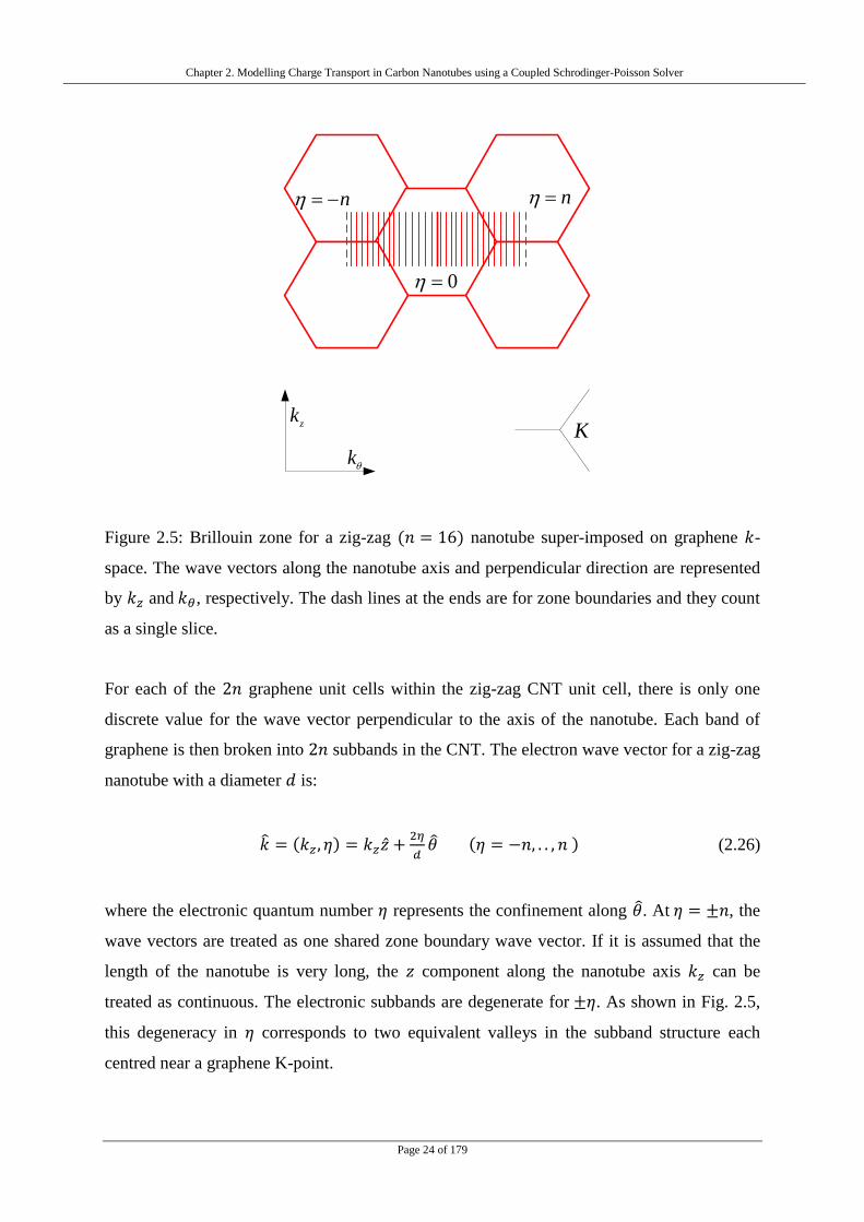
Chapter 2. Modelling Charge Transport in Carbon Nanotubes using a Coupled Schrodinger-Poisson Solver
Page 24 of 179
n n
0
zk
k
K
Figure 2.5: Brillouin zone for a zig-zag nanotube super-imposed on graphene -
space. The wave vectors along the nanotube axis and perpendicular direction are represented
by and , respectively. The dash lines at the ends are for zone boundaries and they count
as a single slice.
For each of the graphene unit cells within the zig-zag CNT unit cell, there is only one
discrete value for the wave vector perpendicular to the axis of the nanotube. Each band of
graphene is then broken into subbands in the CNT. The electron wave vector for a zig-zag
nanotube with a diameter is:
(2.26)
where the electronic quantum number represents the confinement along . At , the
wave vectors are treated as one shared zone boundary wave vector. If it is assumed that the
length of the nanotube is very long, the component along the nanotube axis can be
treated as continuous. The electronic subbands are degenerate for . As shown in Fig. 2.5,
this degeneracy in corresponds to two equivalent valleys in the subband structure each
centred near a graphene K-point.

Chapter 2. Modelling Charge Transport in Carbon Nanotubes using a Coupled Schrodinger-Poisson Solver
Page 25 of 179
Electron conduction is within the delocalized orbitals along the nanotube axis. For this
calculation, the subbands produced from the -antibonding band of graphene is required. The
bandstructure of CNT is calculated from the -orbital nearest-neighbour tight-binding
bandstructure of graphene (described in section 2.1.1). The energy dispersion for a zig-zag
nanotube is:
(2.27)
For the zone-folding method, the conduction electron wavefunction is [7]:
(2.28)
where is the length of the CNT and represents the graphene -antibonding orbitals
normalized over the graphene unit cell.
In the later stage of this chapter, the simulation of electron transport in a CNT at low applied
fields is described. Therefore, the electronic bandstructure of the first few subbands are
required. The - relation of the first three subbands is described using Eq. 2.29 [8].
(2.29)
where is the subband index , is the energy minimum,
is the
effective mass and is the nonparabolicity factor of subband . Table 2.1 shows the
details of Eq. 2.29 parameters. These parameters are a function of the nanotube index because
they are related to the diameter of the nanotube.

Chapter 2. Modelling Charge Transport in Carbon Nanotubes using a Coupled Schrodinger-Poisson Solver
Page 26 of 179
Subbands Energy Minimum Effective Mass Nonparabolicity
Factor
Subband 1
Subband 2
Subband 3
Table 2.1: The bandstructure properties of the first three subbands, where is the
greatest common divisor of and [8].
Having provided a detailed atomic description of CNTs, the modelling techniques used to
simulate electron transport in CNTs at low applied fields are now discussed.
Chapter 2. Modelling Charge Transport in Carbon Nanotubes using a Coupled Schrodinger-Poisson Solver
Page 27 of 179
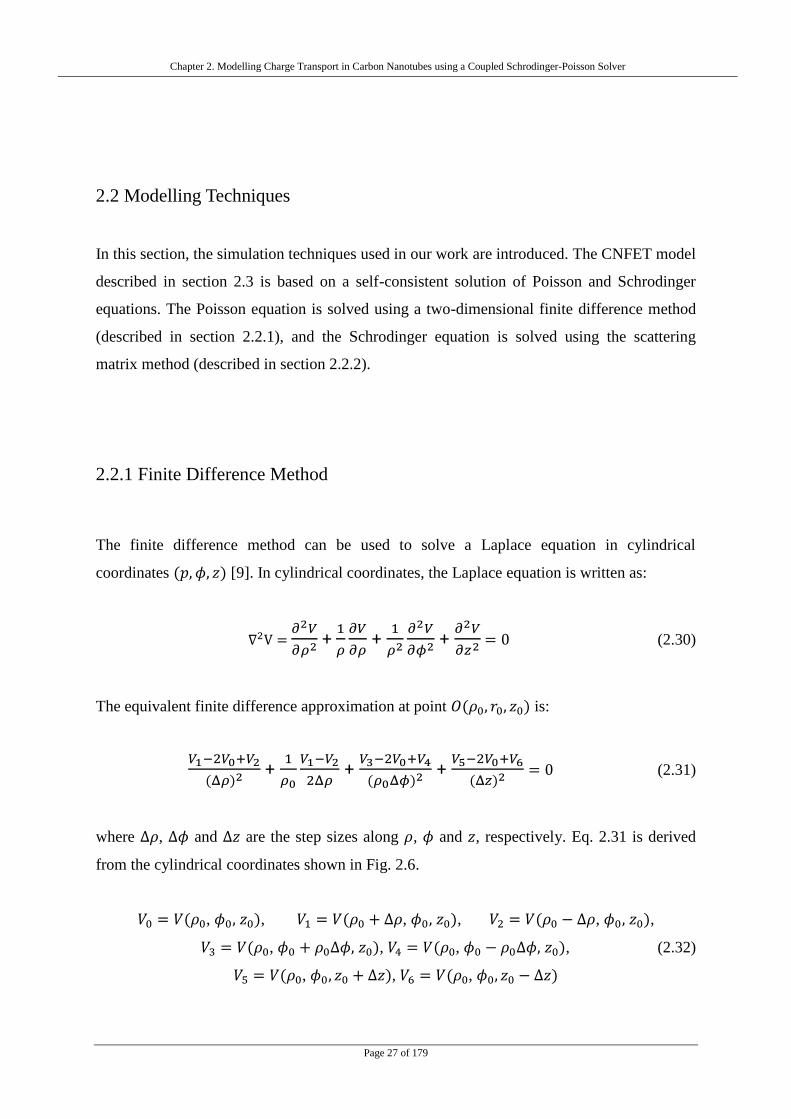
2.2 Modelling Techniques
In this section, the simulation techniques used in our work are introduced. The CNFET model
described in section 2.3 is based on a self-consistent solution of Poisson and Schrodinger
equations. The Poisson equation is solved using a two-dimensional finite difference method
(described in section 2.2.1), and the Schrodinger equation is solved using the scattering
matrix method (described in section 2.2.2).
2.2.1 Finite Difference Method
The finite difference method can be used to solve a Laplace equation in cylindrical
coordinates [9]. In cylindrical coordinates, the Laplace equation is written as:
+
+
+
(2.30)
The equivalent finite difference approximation at point is:
+
+
+
(2.31)
where , and are the step sizes along , and , respectively. Eq. 2.31 is derived
from the cylindrical coordinates shown in Fig. 2.6.
, , , , , ,
, , , , (2.32)
, , ,

Chapter 2. Modelling Charge Transport in Carbon Nanotubes using a Coupled Schrodinger-Poisson Solver
Page 28 of 179
z
y
x
0z
0
0
O
(a)
z
12
3
4
5
6
(b)
i+1
i
i-1
i=0
i=1
j-1 j j+1
h
h
z
ρ
1
2
56 0
Axis of symmetry
(c)
Figure 2.6: (a), (b) - Typical nodes in cylindrical coordinates and (c) Finite difference grid for
an axisymmetric system.

Chapter 2. Modelling Charge Transport in Carbon Nanotubes using a Coupled Schrodinger-Poisson Solver
Page 29 of 179
For an axisymmetric system such as the one described in Fig. 2.6, there is no dependence
of , so . Assuming square nets i.e. , the solution region becomes
discretized. Eq. 2.31 becomes:
(2.33)
Set a point at to give:
(2.34)
(2.35)
There is singularity at and by symmetry, all odd order derivatives must be zero:
(2.36)
(2.37)
By L‟Hopital‟s rule,
(2.38)
The Laplace‟s equation becomes:
(2.39)
Applying finite difference to Eq. 2.39 gives:
(2.40)

Chapter 2. Modelling Charge Transport in Carbon Nanotubes using a Coupled Schrodinger-Poisson Solver
Page 30 of 179
(2.41)
To solve the Poisson equation in cylindrical coordinates, replace the zero on the right hand
side of the Laplace equation with the term .
(2.42)
where is the permittivity, is the step size and is the charge density.
To treat an interface between two media, the boundary condition must be imposed
at the interface, where is the electric displacement field.
2 1
5
6
hh
h
h 1
2
Figure 2.7: Interface between two different media.
Applying Taylor series expansion to points 1, 2 and 5 in medium 1 of Fig. 2.7, gives:
(2.43)

Chapter 2. Modelling Charge Transport in Carbon Nanotubes using a Coupled Schrodinger-Poisson Solver
Page 31 of 179
where superscript (1) denotes medium 1. Summing Eq. 2.30 and Eq. 2.43, gives:
(2.44)
(2.45)
Also, applying the Taylor series to points 1, 2, and 6 in medium 2, gives:
(2.46)
Summing Eq. 2.30 and Eq. 2.46 yields:
(2.47)
(2.48)
Applying the boundary condition or
and solving for gives:
(2.49)

Chapter 2. Modelling Charge Transport in Carbon Nanotubes using a Coupled Schrodinger-Poisson Solver
Page 32 of 179
Having covered the finite difference method used for solving the Poisson equation, the
scattering matrix method used for solving the Schrodinger equation is now described.
2.2.2 Scattering Matrix Method
Classical physics describes the macroscopic world but quantum mechanics describes the
microscopic world of atoms and molecules. Phase randomizing scattering dominates
macroscopic devices so quantum interference effects can be ignored [10]. However, for very
small devices there is a need to use a wave approach to electron transport.
In this work, electron transport in the mesoscopic regime, which is a size scale between
microscopic and macroscopic, is studied. Consider a structure connected to metallic contacts
as shown in Fig. 2.8.
So
urc
e
Dra
in
Channel
L
LF
LTF
RF
RFT
FE
CE
En
erg
y
Position
LF
LTF
RFR
FT
FE
FRE
CE
En
erg
y
Position
qV
Figure 2.8: Flux of carriers injected from each contact into the device (a). A fraction of the
flux from both sides transmits across the device Equilibrium and Under bias.

Chapter 2. Modelling Charge Transport in Carbon Nanotubes using a Coupled Schrodinger-Poisson Solver
Page 33 of 179
The end contacts inject a flux of electrons into the structure. The entire device is then
described by its transmission coefficients, T and T‟, and the net flux through the device is:
(2.50)
where and are the fluxes injected from the left and right contacts, respectively. The
transmission coefficients for the device are determined using a semi-classical calculation.
The scattering matrix theory is derived in terms of carrier fluxes and their backscattering
probabilities [10]. Consider a semiconductor slab with a finite thickness , as shown in Fig.
2.9. Assuming steady state conditions, and are the position-dependent, steady state,
right- and left-directed fluxes. There is a right-directed flux incident on the left face of the
slab and a left-directed flux incident on the right face.
a(z)
b(z)
a(z+∆z)
b(z+∆z)
Figure 2.9: Fluxes of charge carriers incident upon and reflected from a slab of finite
thickness.
In this example, fluxes and that emerge from the slab are to be determined.
These fluxes can be expressed in scattering matrix form, which relates both fluxes emerging
from the slab to the two incident fluxes on the slab:
(2.51)

Chapter 2. Modelling Charge Transport in Carbon Nanotubes using a Coupled Schrodinger-Poisson Solver
Page 34 of 179
where and denote the fraction of the steady-state right- and left-directed fluxes
transmitted across the slab.
The scattering theory can be applied to the device shown in Fig. 2.8. In this case, the device is
divided into a set of thin slabs connected so that the output fluxes from one slab provide the
input fluxes to its neighbouring slabs. The two fluxes injected from the left and right contacts
are used as the boundary conditions. Fig. 2.10 shows two interconnected scattering matrices.
0a 1
a2
a
0b 1
b2
b
Figure 2.10: Two scattering matrices cascaded to produce a single, composite scattering
matrix.
Taking only the fluxes emerging from the set of two scattering matrices, and into
account, the two scattering matrices can be replaced by a single scattering matrix. Assume
that the two scattering matrices have transmission elements , , and
. The elements of
the composite scattering matrix are:
(2.52)
where , etc. Eq. 2.52 describes the multiple reflection processes that occur when a
flux coming from the left or right, transmits across the first slab then backscatters and reflects
from the interiors of the two slabs.

Chapter 2. Modelling Charge Transport in Carbon Nanotubes using a Coupled Schrodinger-Poisson Solver
Page 35 of 179
In real applications, the device is divided into a finite number of scattering matrices. These
matrices are then cascaded two at a time until the entire device is described by a single
scattering matrix. Once this matrix is computed, the current through the device is determined
by subtracting the right- and left-directed fluxes.
In the next section, this modelling technique is applied to a MOS device based on a
semiconducting CNT. The electronic properties of the device are determined from the fluxes
evaluated throughout the device.
2.3 A Two-Dimensional Simulation of Carbon Nanotube Field-Effect
Transistors
In this section, the simulation of electron transport in a semiconducting nanotube using the
CNFET structure is described. Accurate modelling of CNFETs requires a self-consistent
solution of the Poisson and Schrodinger equations. The quantum mechanical treatment of
electron transport is included by solving a one-dimensional Schrödinger equation.
CNFETs are devices with a gate wrapped around the gate dielectric and the nanotube [11].
Here, the coaxial geometry of the CNFET is considered due to the cylindrical nature of
CNTs. Fig. 2.11 shows the structure of the CNFET device described in this work.
Source ContactCarbon Nanotube
Gate Contact
Drain Contact0
0z
tLz
gR
ins
Figure 2.11: The Coaxial Carbon Nanotube FET Geometry.

Chapter 2. Modelling Charge Transport in Carbon Nanotubes using a Coupled Schrodinger-Poisson Solver
Page 36 of 179
Since the source and drain contacts have the same radius as the gate contact, the metallic
cylinder is closed and the simulation technique that is based on a numerical method employed
by John et. al [5] is used to solve for the parameters of the closed system. The device shown
in Fig. 2.11 consists of a semiconducting nanotube surrounded by an insulator with relative
permittivity and a cylindrical, wrap-around gate contact. The ends of the device are
terminated by the source and drain contacts. The device dimensions include the gate
radius , the nanotube radius , the insulator thickness , and the device
length .
In this closed metallic cylinder system, Poisson‟s equation is restricted to just two dimensions
by azimuthal symmetry. To fully specify the geometry of this device, the Poisson‟s equation
as a function of polar and cylindrical coordinates shown in Fig. 2.12, is derived (refer to
Appendix 3).
z
y
x
z
),,( z
Figure 2.12: Cylindrical Coordinates.
In cylindrical coordinates, the Poisson‟s equation restricted to two dimensions by azimuthal
symmetry is:
(2.53)
where ) is the potential within the outer cylinder, is the permittivity and is the
charge density. Although the solution to Eq. 2.53 encompasses the entire volume of the

Chapter 2. Modelling Charge Transport in Carbon Nanotubes using a Coupled Schrodinger-Poisson Solver
Page 37 of 179
device, the longitudinal potential profile along the surface of the nanotube
is mainly required. Knowledge of this potential is required for the carrier transport
calculations.
The solution to Eq. 2.53 is obtained via the finite difference method, which is implemented
by discretizing the spatial domain and using central differencing to generate a linear system
of equations for some known charges, and subject to the boundary conditions. The boundary
conditions for the CNFET device are:
(2.54)
(2.55)
(2.56)
where is the work function, is the electron charge, is the gate-source voltage and
is the drain-source voltage. In our system, we replace the values of the potential at the device
boundaries with the boundary conditions shown in Eq. 2.54 - Eq. 2.56. A detailed procedure
for computing the electrostatic potential within the CNFET structure is described in
Appendix 4.
The charge distribution on the surface of the nanotube is obtained by solving the Poisson
equation coupled with the time-independent Schrödinger equation:
(2.57)
where is the wavefunction of the carrier with an Energy , is the effective mass
obtained from the bandstructure of the zig-zag nanotube and is the local effective potential
seen by the carriers.

Chapter 2. Modelling Charge Transport in Carbon Nanotubes using a Coupled Schrodinger-Poisson Solver
Page 38 of 179
(2.58)
where is the electron affinity of CNT.
The charge density in the CNFET device is given by:
(2.59)
where is the Dirac delta function in cylindrical coordinates, and are computed
from the Schrodinger equation. A numerical solution of Eq. 2.57 is found at any given
energy . Schrodinger‟s equation is solved using the scattering matrix method in which a
numerical solution is propagated by cascading matrices as described in section 2.2.2.
A detailed description of the grid implementation for the model device is provided in
Appendix 5. The entire system is divided into grids and for each grid the electron
wavefunction is expressed as:
(2.60)
where is the wavevector, and are the amplitudes of the wavefunctions. The
wavefunction and its derivative are matched on the boundary between intervals and
using the relations:
(2.61)
(2.62)
As described in section 2.2.2, the relationship between and is
obtained using:

Chapter 2. Modelling Charge Transport in Carbon Nanotubes using a Coupled Schrodinger-Poisson Solver
Page 39 of 179
(2.63)
where is the transpose of the matrix , is the scattering coefficient, and
are the wavefunctions in the source and drain contacts, respectively. When computing the
wavefunctions for the source injection, the amplitude of the wavefunction at the drain end is
set to zero. An analogous calculation is performed when considering the drain injection.
The Landauer equation is expected to hold for the flux and the probability current equated
to the Landauer current [12]:
(2.64)
(2.65)
(2.66)
where is the Fermi-Dirac carrier distribution in the source and T is the transmission
probability described by:
(2.67)
The normalization condition is:
(2.68)

Chapter 2. Modelling Charge Transport in Carbon Nanotubes using a Coupled Schrodinger-Poisson Solver
Page 40 of 179
The total carrier density in the system is computed from the normalized wavefunctions. In
order to obtain the carrier distribution along the surface of the nanotube, is integrated over
all possible energy levels.
(2.69)
(2.70)
where is the bottom of the energy band, is the vacuum energy level, is the
electrons source injection, is the electrons drain injection, is the holes source
injection, and is the holes drain injection. Eq. 2.69 and Eq. 2.70 can be solved using the
right-point rectangle rule [13] or the adaptive Simpson‟s method [14].
The right-point rectangle rule is expressed as:
(2.71)
In this approach, the interval [ , ] is simply divided into equidistant points and the
Schrodinger equation is solved at these points. This method can only give an accurate result if
a large number of points are allocated within the intervals. This will require an extremely
large computing time to achieve a converged carrier density. Narrow resonances of the
wavefunction may occur at certain energy levels when the potential profile on the CNT
channel changes. These narrow resonances will lead to a sudden change of the carrier
concentration and result in longer simulation time or even worse an oscillated and non-
converged charge density. This problem can be avoided by using a numerical integration
method that refines the grid in the region of resonances.
The integrations were performed using the adaptive Simpson‟s method with different
subdivided intervals defined [14]. The adaptive Simpson‟s method is expressed as:

Chapter 2. Modelling Charge Transport in Carbon Nanotubes using a Coupled Schrodinger-Poisson Solver
Page 41 of 179
(2.72)
(2.73)
where
If , where is a predefined tolerance, the algorithm calls for further division
of the integration interval into two, and the adaptive Simpson's method is applied to each
subinterval in a recursive manner. In this approach, the points in the integration intervals are
non-equidistant, so there are many points around the resonances while there are only few
points in other regions.
Simulation Procedure
To start the simulation, the initial charge density inside the device is guessed, usually zero.
The next step is to compute the electron potential inside the device by solving Poisson‟s
equation. The new charge density in the device is computed by using the scattering matrix
method to solve the Schrodinger equation. This new charge density is then used to solve the
Poisson equation again and these steps are repeated a number of times until the new value of
the charge density match the older one. At this point, the criterion for convergence of the
system is achieved and other properties of the device are observed via numerical integrations.
Fig. 2.13 shows the flow chart of the simulation procedure.

Chapter 2. Modelling Charge Transport in Carbon Nanotubes using a Coupled Schrodinger-Poisson Solver
Page 42 of 179
Initial guess of n(r)Solve the Poisson
Equation -> V(r)
Final ResultSolve the Schrodinger
Equation -> New n(r)
Self Consistent?
Figure 2.13: Iterative procedure for computing electrostatics and charge transport self-
consistently.
2.4 Simulation Results
The carbon nanotube used for this simulation is a zig-zag nanotube with indices
. The nanotube diameter is and the corresponding bandgap is .
Other parameters of the device include the nanotube length , dielectric thickness
and . The nanotube ends are terminated with silver contacts
having a work function of . The electron affinity is , and the nanotube is
presumed to have a free-space relative permittivity ( ). The electron effective mass
is calculated from the bandstructure properties of the nanotube (as described in table 2.1) and
it is for both electrons and holes [6][7], where is the free electron mass.
Now, the result of a simulation based on the theory described in section 2.3 is analysed. Fig.
2.14 shows the conduction band profile when the applied gate voltage is varied. A positive
gate bias pulls the conduction band down, allowing more propagating modes in the channel.

Chapter 2. Modelling Charge Transport in Carbon Nanotubes using a Coupled Schrodinger-Poisson Solver
Page 43 of 179
Figure 2.14: Simulation of the potential energy seen by the electrons at different gate bias for
the equilibrium condition ( . Conduction band edge along the length of the device
for , and .
The potential profile for applied and is shown in Fig. 2.15. Fig. 2.16 shows
the electron density when the drain-source voltage is varied and a constant gate-source
voltage of is applied. The electrons in the channel are from the source and drain
contacts and they are drawn into the nanotube by tunneling through the barriers at the
contacts. When the system is in equilibrium ( , the charge carrier concentration is
evenly distributed throughout the device, following the shape of the conduction band profile.
Interference effects on the charge distributions are observed when the system is out of
equilibrium. The electron concentration in the channel reduces as increases because
evanescent states dominate the electron concentrations near the device contacts and the effect
is seen on the local potential.

Chapter 2. Modelling Charge Transport in Carbon Nanotubes using a Coupled Schrodinger-Poisson Solver
Page 44 of 179
Figure 2.15: Conduction band edge along the device length for ,
and . The energies are with respect to the source Fermi level.
Figure 2.16: Simulation of the carrier density as a function of position and varying
when .
0
0.5
1
0 510 15 20
-6
-5
-4
-3
-2
-1
0
Vds
(V)
Z (nm)
Ele
ctr
on
de
nsity (
108
/m)

Chapter 2. Modelling Charge Transport in Carbon Nanotubes using a Coupled Schrodinger-Poisson Solver
Page 45 of 179
The simulation method allows the inclusion of quantum mechanical reflection for the
thermionic component of the flux. The total carrier distribution within the nanotube is
determined by the action of reflections at the barriers near the contacts on the injected
carriers. Carriers above the potential barrier are often assumed to have a transmission
probability closed to unity. This approximation does not hold in general since there is a
significant reflection when the minimum integration energy (taken to be below the
metal Fermi level [5]) is much lower than the conduction band edge. As shown in Fig. 2.17,
for energies that are well above the barrier height, the transmission coefficient is oscillatory
approaching unity as becomes large.
(a) (b)
Figure 2.17: Transmission probabilities for electrons (a), and the corresponding conduction
band edge (b) at and .
Fig. 2.18 shows the drain I-V characteristics for the model device. For an applied gate bias of
0.5V, the nanotube saturation current is achieved at a drain bias of 0.2V. The reflecting action
at the nanotube-drain interface limits the expected full saturation current of . There is a
significant reflection when the minimum integration energy is much lower than the
conduction band edge.
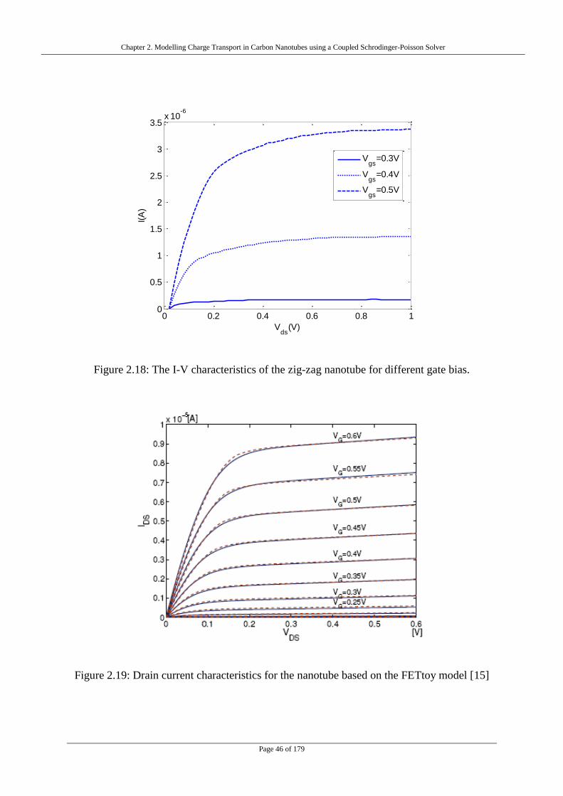
Chapter 2. Modelling Charge Transport in Carbon Nanotubes using a Coupled Schrodinger-Poisson Solver
Page 46 of 179
Figure 2.18: The I-V characteristics of the zig-zag nanotube for different gate bias.
Figure 2.19: Drain current characteristics for the nanotube based on the FETtoy model [15]
0 0.2 0.4 0.6 0.8 10
0.5
1
1.5
2
2.5
3
3.5x 10
-6
Vds
(V)
I(A
)
Vgs
=0.3V
Vgs
=0.4V
Vgs
=0.5V
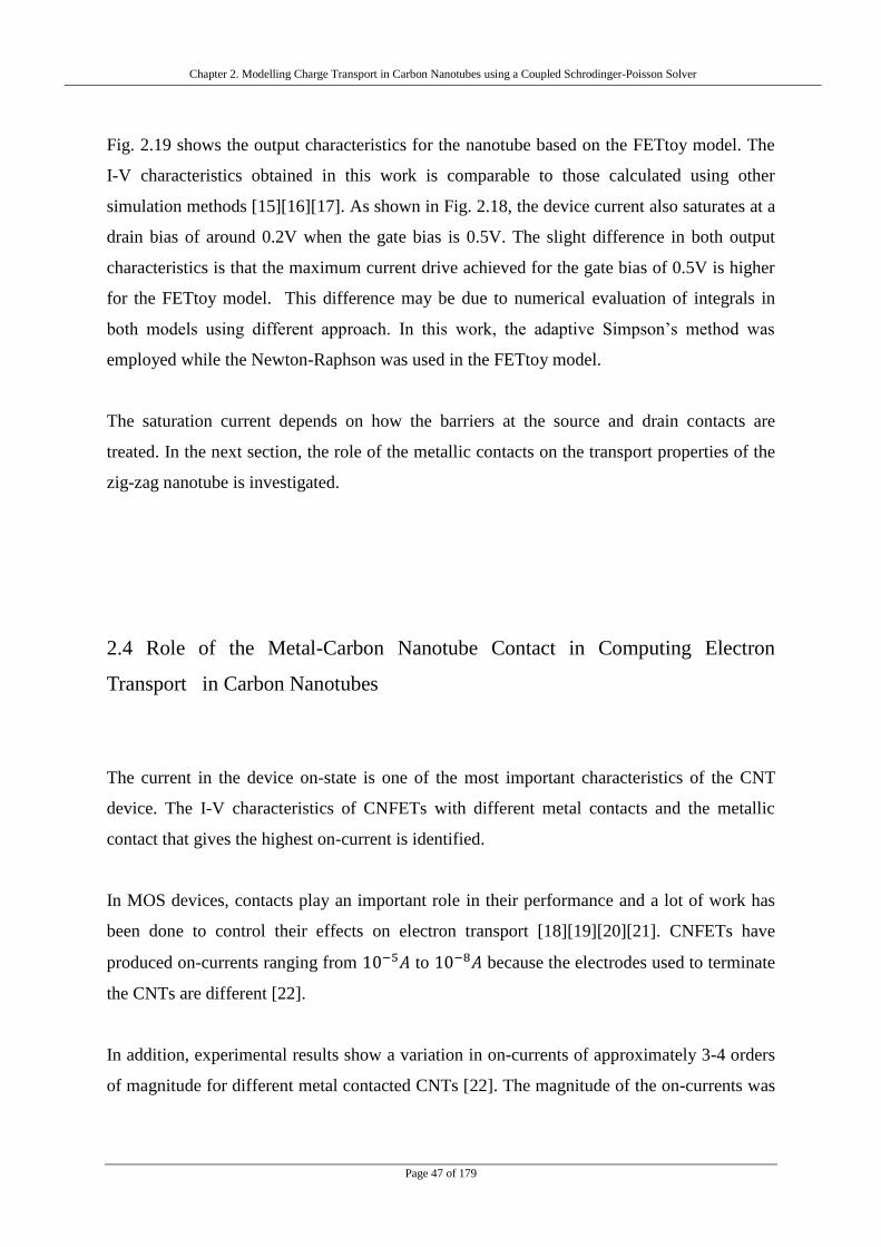
Chapter 2. Modelling Charge Transport in Carbon Nanotubes using a Coupled Schrodinger-Poisson Solver
Page 47 of 179
Fig. 2.19 shows the output characteristics for the nanotube based on the FETtoy model. The
I-V characteristics obtained in this work is comparable to those calculated using other
simulation methods [15][16][17]. As shown in Fig. 2.18, the device current also saturates at a
drain bias of around 0.2V when the gate bias is 0.5V. The slight difference in both output
characteristics is that the maximum current drive achieved for the gate bias of 0.5V is higher
for the FETtoy model. This difference may be due to numerical evaluation of integrals in
both models using different approach. In this work, the adaptive Simpson‟s method was
employed while the Newton-Raphson was used in the FETtoy model.
The saturation current depends on how the barriers at the source and drain contacts are
treated. In the next section, the role of the metallic contacts on the transport properties of the
zig-zag nanotube is investigated.
2.4 Role of the Metal-Carbon Nanotube Contact in Computing Electron
Transport in Carbon Nanotubes
The current in the device on-state is one of the most important characteristics of the CNT
device. The I-V characteristics of CNFETs with different metal contacts and the metallic
contact that gives the highest on-current is identified.
In MOS devices, contacts play an important role in their performance and a lot of work has
been done to control their effects on electron transport [18][19][20][21]. CNFETs have
produced on-currents ranging from to because the electrodes used to terminate
the CNTs are different [22].
In addition, experimental results show a variation in on-currents of approximately 3-4 orders
of magnitude for different metal contacted CNTs [22]. The magnitude of the on-currents was

Chapter 2. Modelling Charge Transport in Carbon Nanotubes using a Coupled Schrodinger-Poisson Solver
Page 48 of 179
observed to be dependent on the work functions of the metal used to terminate the nanotube
[22]. The variation in on-currents was linked to the electron injection into the nanotube,
which is dependent on the line-up of the metal Fermi level and the conduction band in the
nanotube.
Another experimental issue is that a nanotube could be end-bonded to the metal as shown in
Fig. 2.20a or it could lay on the metal surface and be side-contacted as shown in Fig. 2.20b.
The contact geometry realised defines the coupling strength, which influences electron
transport at the metal/nanotube interface [19][23].
GoldGoldCNT
(a)
Gold
Gold
Gold2
SiO
CN
T
(b)
Figure 2.20: A carbon nanotube „end bonded‟ to the metal, a carbon nanotube
forming „side contacts‟ on gold electrodes
Here the performance of CNFETs modelled with different metallic contacts is analysed.
Silver , Iron and Gold are the metals used for this simulation. The work
functions for , and are , and , respectively. As before, the
Poisson and Schrodinger equations are self-consistently solved using finite difference

Chapter 2. Modelling Charge Transport in Carbon Nanotubes using a Coupled Schrodinger-Poisson Solver
Page 49 of 179
technique and scattering matrix method, respectively. The transmission probability for the
electrons is then computed from the solution of the Schrodinger equation. Since the
metal/nanotube interface introduces boundary conditions in the solution of the Schrodinger
equation, the transmission probability is dependent on the metal work function.
Simulation Results
The transport properties of the zig-zag nanotube are examined when different metal contacts
terminate its ends. Electron transport from the metal contact into the nanotube is dominated
by quantum mechanical tunnelling, thereby increasing the resistance of the contact. The
conduction band profile is analysed and we look closely at the barriers near the end contacts.
At the metal/nanotube interface, the barrier height depends on the metal work function.
Fig. 2.21 shows the conduction band edge for the CNFETs with different metal contacts. The
band bending occurs over a length scale known as the Debye length . At this length scale,
the electrons screen out the applied fields (refer to Appendix 7 for details). In the devices,
when and , is approximately , and for ,
and contacts, respectively.
The device current depends on and the barrier height at the metal/nanotube interface. If
is small, electrons tunnel through the barriers at the contact more readily and this will lead to
an increased current.

Chapter 2. Modelling Charge Transport in Carbon Nanotubes using a Coupled Schrodinger-Poisson Solver
Page 50 of 179
(a) (b)
(c) (d)
(e) (f)
Figure 2.21: The band bending for the metal/nanotube junction at ,
and the transmission probability for electrons at . [ with
- (a), (b)], [ with - (c), (d)] and [ with - (e), (f)]. The
band bending occurs over a length scale .

Chapter 2. Modelling Charge Transport in Carbon Nanotubes using a Coupled Schrodinger-Poisson Solver
Page 51 of 179
As shown in Fig. 2.22, the on-currents of the zig-zag nanotube vary for different metal
contacts. On comparing the I-V characteristics of the devices, it was observed that on-current
is higher when is used as the device contacts. This is expected as and the barrier height
for are smaller when compared to those of and . When is used as the metal
contacts, the maximum current drive is achieved at a lower drain voltage compared to
and . As shown in Fig. 2.22, a full current saturation is only achieved for contacts but
the current saturates at a larger drain voltage . Based on the observed on-current and
current saturation, an optimum CNFET performance is achieved when is used as the
nanotube end contacts.
Figure 2.22: Plot of CNFETs I-V characteristics as a function of metal contacts at .
0 0.2 0.4 0.6 0.8 10
0.5
1
1.5
2
2.5x 10
-5
Vds
(V)
I ds (
A)
Ag Contacts
Fe Contacts
Au Contacts

Chapter 2. Modelling Charge Transport in Carbon Nanotubes using a Coupled Schrodinger-Poisson Solver
Page 52 of 179
Figure 2.23: The ideal output characteristics of the device without contact effects [15].
The differences in the output characteristics of the devices can be understood from the
relationship between the drain current and the transmission probability for electrons. As
shown in Fig. 2.21, the transmission probability when the energy is greater than is
higher for and stays constant afterwards (as described by the spikes). However, the
transmission probability for and is still increasing for these energies, and this prevents
full current saturation. The trends for the I-V characteristics follow that of the metal work
functions. Therefore, the operation of CNFETs can be controlled by modulating the
tunnelling barriers at the contacts. Fig. 2.23 shows the output characteristics of the device
without the contact effects. In the ideal case, a full current saturation is achieved for a drain
bias of around .

Chapter 2. Modelling Charge Transport in Carbon Nanotubes using a Coupled Schrodinger-Poisson Solver
Page 53 of 179
2.5 Conclusions
The bandstructure of graphene is calculated through a tight-binding Hamiltonian. Using the
zone-folding method ZFM [8], the bandstructure of CNTs is obtained from the -orbital
nearest-neighbour tight-binding bandstructure of graphene [6].
Methods for modelling charge transport in a CNT have been discussed and illustrated using
the Schrodinger-Poisson solver. Poisson‟s equation is solved self-consistently with
Schrodinger‟s equation using the finite difference and scattering matrix techniques,
respectively. The scattering matrix method enables resonance effects to be taken into account.
A fully wrapped around gate is assumed to improve immunity to short channel effects [24].
The drain I-V characteristics of the CNFET device suggest there is a reflecting action at the
nanotube-drain contact interface influencing the current saturation of the device.
The role of metal-nanotube contacts in computing electron transport in CNTs has been
investigated. Simulation results show that contacts play a dominant role in the performance of
CNFETs. In the later stage of this thesis, electron transport in CNTs is investigated using a
method that avoids the influence of metal contacts.
In the next Chapter, a simulation of electron transport in a graphene nanoribbon is described
and its output characteristics compared to that of a CNFET.

Chapter 2. Modelling Charge Transport in Carbon Nanotubes using a Coupled Schrodinger-Poisson Solver
Page 54 of 179
2.6 References
[1] Z. Chen, D. Farmer, S. Xu, R. Gordon, P. Avouris, and J. Appenzeller, Externally
Assembled Gate-All-Around Carbon Nanotube Field-Effect Transistor, IEEE Electron
Device Letters, Vol. 29, No. 2, February 2008.
[2] T. Iwai, Y. Awano, Carbon Nanotube Bumps for Thermal and Electric Conduction in
Transistor, FUJITSU Sci. Tech. J., 43, 4, pp.508-515, October 2007.
[3] H. Wei, N. Patil, A. Lin, H. S. Philip Wong, S. Mitra, Monolithic Three-Dimensional
Integrated Circuits using Carbon Nanotube FETs and Interconnects, Electron Devices
Meeting (IEDM), December 2009 IEEE International, DOI:
10.1109/IEDM.2009.5424292.
[4] G. F. Close, S. Yasuda, B. Paul, S. Fujita, and H. S. Philip Wong, A 1 GHz Integrated
Circuit with Carbon Nanotube Interconnects and Silicon Transistors, Nano Lett.,
2008, 8 (2), pp 706–709.
[5] D. L. John, L. C. Castro, P. J. S. Pereira, and D. L. Pulfrey, A Schrodinger-Poisson
Solver for Modeling Carbon Nanotube FETs, Proc. NSTI Nanotech, vol. 3, pp. 65-68,
2004.
[6] D. Gunlycke and C. T. White, Tight-binding energy dispersions of armchair-edge
graphene nanostrips, Physical Review B, vol. 77, pp. 115-116, 2008.
[7] M. S. Dresselhaus, G. Dresselhaus and Ph. Avouris (eds.), Carbon Nanotubes
Synthesis, Structure, Properties, and Applications (Topics in Applied Physics; v. 80),
2001, ISBN 3540410864.
[8] G. Pennington and N.Goldsman, Semiclassical Transport and Phonon Scattering of
Electrons in Semiconducting Carbon Nanotubes, Phys. Rev. B 68, 045426 (2003).
[9] M. N.O. Sadiku, Numerical Techniques in Electromagnetics, CRC Press, Boca Raton,
1992.
[10] M. Lundstrom, Fundamentals of Carrier Transport, Second Edition, Cambridge
University Press, 2000.

Chapter 2. Modelling Charge Transport in Carbon Nanotubes using a Coupled Schrodinger-Poisson Solver
Page 55 of 179
[11] L. C. Castro, D. L. John, and D. L. Pulfrey, An improved evaluation of the DC
performance of carbon nanotube field-effect transistors, Smart Mater. Struct. 15
(2006) S9–S13.
[12] D. L. Pulfrey, Carbon Nanotube Field-Effect Transistors and their Possible
Applications, Nano Electronics Group, May 30, 2008, Pisa.
[13] C. J. Zarowski, An Introduction to Numerical Analysis for Electrical and Computer
Engineers, A John Wiley & Sons, Inc. Publication, ISBN - 0471467375, 2004.
[14] M. Pourfath, H. Kosina, and S. Selberherr, A fast and stable Poisson-Schrodinger
solver for the analysis of carbon nanotube transistors, Journal of Computational
Electronics, vol. 5, pp. 155-159, 2006.
[15] T. J Kazmierski, D. Zhou and B. M Al-Hashimi, A Fast, Numerical Circuit-Level
Model of Carbon Nanotube Transistor, Sch. of Electron. & Comput. Sci.,
Southampton Univ., Southampton, Nanoscale Architectures 2007, NANOSARCH
2007 IEEE International Symposium, pp. 33-37.
[16] A. Hazeghi, T. Krishnamohan, and H. S. Philip Wong, Schottky-Barrier Carbon
Nanotube Field-Effect Transistor Modeling, IEEE Transactions On Electron Devices,
Vol. 54, No. 3, March 2007.
[17] T. J. Kazmierski, D. Zhou and B. M. Al-Hashimi, HSPICE implementation of a
numerically efficient model of CNT transistor, Forum on Specification and Design
Languages (FDL 2009), September 22-24, 2009, Germany.
[18] Z. Zhang, X. Liang, S. Wang, K. Yao, Y. Hu, Y. Zhu, Q. Chen, W. Zhou, Y. Li, Y.
Yao, J. Zhang, and L.-Mao Peng, Doping-Free Fabrication of Carbon Nanotube Based
Ballistic CMOS Devices and Circuits, Nano Letters, Vol. 7, No. 12, pp. 3603-3607,
2007.
[19] P. Tarakeshwar, J. J. Palacios, and Dae M. Kim, Interface Study of Metal Electrode
and Semiconducting Carbon Nanotubes: Effects of Electrode Atomic Species, IEEE
Transactions on Nanotechnology, Vol. 7, No. 2, March 2008.
[20] Y. He, J. Zhang, S. Hou, Y. Wang, and Z. Yu, Schottky barrier formation at metal
electrodes and semiconducting carbon nanotubes, Applied Physics Letters 94,
093107, 2009.
[21] K. Nagashio, T. Nishimura, K. Kita, and A. Toriumi, Contact resistivity and current
flow path at metal/graphene contact, Applied Physics Letters 97, 143514, 2010.

Chapter 2. Modelling Charge Transport in Carbon Nanotubes using a Coupled Schrodinger-Poisson Solver
Page 56 of 179
[22] S. Chu Lim, J. Ho Jang, D. Jae Bae, G. Hee Han, S. Lee, I. Yeo, and Y. Hee Lee,
Contact resistance between metal and carbon nanotube interconnects: Effect of work
function and wettability, Applied Physics Letters 95, 264103, 2009.
[23] N. Peng, H. Li and Q. Zhang, Nanoscale Contacts between Carbon Nanotubes and
Metallic Pads, ACS Nano, 3 (12), pp. 4117–4121, 2009.
[24] Y. Ouyang, Y. Yoon, and J. Guo, Scaling Behaviors of Graphene Nanoribbon FETs:
A Three-Dimensional Quantum Simulation Study, Electron Devices, IEEE
Transactions on, vol. 54, pp. 2223-2231, 2007.

Chapter 3. Comparison of the Current-Voltage Characteristics of MOS Devices Based on Carbon Nanotubes and Graphene
Page 57 of 179
Chapter 3
Comparison of the Current-Voltage Characteristics of MOS Devices Based
on Carbon Nanotubes and Graphene
3.1 Introduction
Simulations of the electronic properties of CNFETs suggest that they have great potential in
future high speed electronic systems [2][3]. However, in practice, it is difficult to control the
chirality of carbon nanotubes and the structures cannot readily be integrated into an electronic
system. The chirality is important because the energy bandgap of a semiconducting CNT is a
function of it [4].
Recently, graphene [5], which is a single sheet of graphite, has been created in the laboratory
for the first time. Although graphene has been studied theoretically for many years it was
thought to be too unstable to exist in its basic form. The discovery of stable graphene at the
University of Manchester in 2004 has led to the realistic prospect of its utilization within
electronic devices. The advantage of graphene is that it is compatible with the planar
technology employed within the semiconductor industry. Like CNTs, graphene exhibits high
electron mobilities [5], μ, in excess of and it can be metallic or
semiconducting.
When tailored to less than wide graphene nanoribbons may open a band gap due to
the electron confinement. Electronic states of the graphene nanoribbon largely depend on the
edge structures and the width [6]. There are two main types of nanoribbon, known as
Chapter 3. Comparison of the Current-Voltage Characteristics of MOS Devices Based on Carbon Nanotubes and Graphene
Page 58 of 179
armchair-edge and zigzag-edge, depending on the arrangements of carbon atoms along the
nanoribbon edges.
One of the most important potential applications of graphene is as the channel for electron
transport in a MOS structure. Structures of this kind have been demonstrated experimentally
[7] using epitaxially synthesized graphene on silicon carbide substrates. This work describes
the simulation of an armchair-edge graphene based MOS transistor using a coupled
Schrödinger-Poisson solver and compares the result with the characteristics of CNT based
MOSFETs described in Chapter 2.
3.2 Model - Graphene Nanostrip Field Effect Transistors (GFETs)
A semiconducting armchair-edge graphene nanoribbon is used as the channel of the device to
be modelled. The band structure is obtained through a tight-binding Hamiltonian of the
armchair-edge nanoribbon that includes the summation of the first-nearest-neighbour (1NN)
Hamiltonian, third-nearest-neighbour (3NN) Hamiltonian, 3NN truncation Hamiltonian and
the 1NN edge distortion Hamiltonian [8].
Charge transport in graphene is investigated through the self-consistent solution of the charge
and local electrostatic potential. The quantum mechanical treatment of electron transport is
included by solving a one-dimensional (1D) Schrödinger‟s equation. A graphene field-effect
transistor (GFET) based on the structure shown in the Fig. 3.1 is modelled. This device
consists of a semiconducting nanoribbon with a wrap around gate at four faces of the
rectangular geometry. A dielectric with relative permittivity separates the semiconductor
region of the device from the surrounding gate contact. The ends of the device are terminated
by the source and drain contacts. Device parameters include the length (along x-direction) of
the nanoribbon, its width (along z-direction) and the thickness of the insulator separating
the graphene from the gate contact.

Chapter 3. Comparison of the Current-Voltage Characteristics of MOS Devices Based on Carbon Nanotubes and Graphene
Page 59 of 179
Figure 3.1: Cubical geometry of Graphene FET.
The potential profile in the entire model is obtained from the solution of the three-
dimensional Poisson‟s equation in a rectangular system given by:
(3.1)
where and are the potential and charge density, respectively. The width
of the nanoribbon is divided into unit cells allowing the graphene sheet to be treated as a
quasi-one-dimensional conductor. The charge distribution on the surface of the material is
obtained by solving the time-independent Schrödinger equation given by:
(3.2)
where is the wavefunction of the carrier having an energy and is the effective
mass obtained from the bandstructure of the nanoribbon and is the same for both electrons
and holes due to symmetry [9]. U is the local potential.

Chapter 3. Comparison of the Current-Voltage Characteristics of MOS Devices Based on Carbon Nanotubes and Graphene
Page 60 of 179
3.3 Device Simulation
The simulation is based on a numerical procedure employed by John et. al. [2]. Poisson‟s
equation is solved using a finite difference method applying central differencing, forward
differencing and backward differencing where applicable in the grid system. In matrix form
Poisson‟s equation is written as
(3.3)
where and are the potential and charge density vectors, respectively, is the length of
the grid and is a matrix generated from the finite difference method. Boundary conditions
for the potential are defined by the terminal voltages and work functions.
The computed potential on the surface of the graphene sheet is defined by the vacuum level,
. The potential energy seen by the electrons and holes is given by:
(3.4)
(3.5)
where and are electron affinity and graphene band gap, respectively.
The charge distribution on the graphene surface is obtained by solving the Schrödinger
equation using the scattering matrix. The charge density in the model device is given by
(3.6)
where is the electron charge, and computed from Eq. 3.15 and Eq. 3.16 are the
number of electrons and holes, respectively, in the graphene as a function of position. The

Chapter 3. Comparison of the Current-Voltage Characteristics of MOS Devices Based on Carbon Nanotubes and Graphene
Page 61 of 179
grid system used in the simulation is based on a series of matrices; the wavefunction
and its derivative are matched at the boundaries between the intervals and yielding a
stable system [10]. The boundary conditions give:
(3.7)
(3.8)
Boundary conditions for the wavefunctions at the contacts are given by:
(3.9)
(3.10)
where and are the wavefunction at source and drain, respectively, , , and are
the amplitudes of the wavefunctions and , are the wavevectors in the source and drain,
respectively. The relationship between the amplitude of the wavefunctions and
is given by the transfer matrix:
(3.11)
The Landauer expression [10] holds for the flux and equals the probability current yielding:
(3.12)
where is the Fermi-Dirac carrier distribution in the source, and is the transmission
probability specified by:
(3.13)
Substituting the expression for the transmission probability into the Landauer equation results
in the normalization

Chapter 3. Comparison of the Current-Voltage Characteristics of MOS Devices Based on Carbon Nanotubes and Graphene
Page 62 of 179
(3.14)
By including the source and drain injection components, the normalized wavefunction gives
the total carrier density in the device. The carrier density on the graphene sheet is calculated
by integrating over all possible energies levels.
(3.15)
(3.16)
Here is the conduction band edge, is the vacuum energy level, and are
the electron wavefunctions within the source and drain, respectively while and are
the equivalent wavefunctions for holes. The integration is performed using the procedure
described in ref. 3.
Using a numerical damping factor, the coupled Schrödinger-Poisson equation model was
solved iteratively. An initial assumption of zero charge on the graphene surface was made
and the electrostatic potential computed from Poisson‟s equation. A new charge density is
computed using the calculated electrostatic potential . The new charge density
is
used for the calculation of the new potential and finally the new potential is
calculated as:
(3.17)
where . The convergence of the system is achieved when the defined criterion is
met (i.e. error less than10-5
).

Chapter 3. Comparison of the Current-Voltage Characteristics of MOS Devices Based on Carbon Nanotubes and Graphene
Page 63 of 179
Figure 3.2: Normalised potential updates after each iteration.
3.4 Simulation Results
The graphene nanoribbon used in the study has dimensions . Carbon
nanotubes are formed by rolling the nanoribbon resulting in tubes of radius . For both
structures the work-functions of the source and drain regions were taken to be and the
conduction band edge in the channel in equilibrium is above the Fermi energy level.
The work function is chosen to be consistent with the value for silver used in the
experimental work reported in ref [11]. Only the first subband was considered as the energies
of the upper subbands exceed the drain voltage in the structures used in this simulation. A
single effective mass was used in the model devices to allow comparison of their output
characteristics. The effective mass was for both electrons and holes, where, is
the free electron mass [12].
Fig. 3.3a shows a three-dimensional (3D) plot of the electron potential energy within the
graphene sheet with = 0V and = 0.5V. The electron potential energy, represented by
the conduction band edge, is lower at the edges of the sheet due to the wrap around gate.

Chapter 3. Comparison of the Current-Voltage Characteristics of MOS Devices Based on Carbon Nanotubes and Graphene
Page 64 of 179
Increasing lowers the conduction band edge in the central region as shown in Fig. 3.3b.
Cross-sections of the electron energy profiles along the edge of the sheet and in the centre of
the channel, giving a clearer picture of the effect of drain voltage on electron energy, are
shown in Figs. 3.3c and 3.3d respectively.
(a) (b)
(c) (d)
Figure 3.3: Simulation of the potential energy seen by the electrons at (a) 3D
view of the conduction band edge at (b) 3D view of the conduction band edge at
(c) Conduction band edge along the length of the device for different at the
edge of the graphene sheet (d) Conduction band edge along the length of the device for
different at the centre of the graphene sheet.

Chapter 3. Comparison of the Current-Voltage Characteristics of MOS Devices Based on Carbon Nanotubes and Graphene
Page 65 of 179
Figures 3.4a and 3.4b show the electron density throughout the graphene sheet resulting from
tunneling through the potential barrier at the contact. When the , the electron
density is higher at the edges than in the centre, a result consistent with the variation of the
conduction band edge. As the drain voltage is increased to , the electron density falls
within the centre and at the edges. Again, this can be seen more clearly from the cross-
sections of the energy density profile through the centre of the device and at the edges. This
result can be compared with that obtained in chapter 2 for a carbon nanotube structure.
(a) (b)
(c) (d)
Figure 3.4: Simulation of the carrier density at . (a) 3D view of the net carrier
density as a function of position at . (b) 3D view of the net carrier density as a
function of position at . (c) Cross-section of carrier density for different at the
centre of graphene sheet (d) Cross-section of carrier density for different at the edge of
the graphene sheet.
0
1
2
3
0
5
10
15
20
0
2
4
6
8
Z (nm)X (nm)
Ele
ctr
on
den
sity
(1
017/m
2)
0
1
2
3
0
5
10
15
20
0
2
4
6
8
10
12
Z (nm)X (nm)
Ele
ctr
on
den
sity
(1
017/m
2)
0 2 4 6 8 10 12 14 16 18 200
0.5
1
1.5
2
2.5
3
3.5
4
4.5
X (nm)
Ele
ctr
on
den
sity
(1
017/m
2)
Vds
=0.0V Vgs
=0.5V
Vds
=0.4V Vgs
=0.5V
0 2 4 6 8 10 12 14 16 18 200
2
4
6
8
10
12
X (nm)
Ele
ctr
on
den
sity
(1
017/m
2)
Vds
=0.0V Vgs
=0.5V
Vds
=0.4V Vgs
=0.5V

Chapter 3. Comparison of the Current-Voltage Characteristics of MOS Devices Based on Carbon Nanotubes and Graphene
Page 66 of 179
Figures 3.5 (a) & (b), respectively, show the output characteristics of MOSFETs for a
graphene ribbon and a carbon nanotube. The width of the graphene ribbon equals the
circumference of CNT. Comparing the I-V characteristics of these devices it is observed that
for graphene the maximum current drive is achieved at a much lower drain bias. This result
suggests that circuits based on graphene MOSFETs may have a superior switching
performance than those based on CNTs. The saturation currents for the graphene and CNT
devices are and , respectively. The low bias conductance of the devices can be
approximated from the slope of the I-V characteristics. Based on this approximation, the
maximum conductance for the graphene and CNT devices are and , respectively.
(a) (b)
Figure 3.5: I-V characteristics of Graphene (a) and CNT (b)
The physical origin of the difference in the output characteristics can be understood by
considering the relationship between the drain current, , and the transmission probability,
and Fermi Dirac function :
(3.18)
Figures 3.6 (a) – (f) show plots of , and for the graphene and CNT
based MOSFETs at three drain-source voltages, and . Figures 2.25 (a),
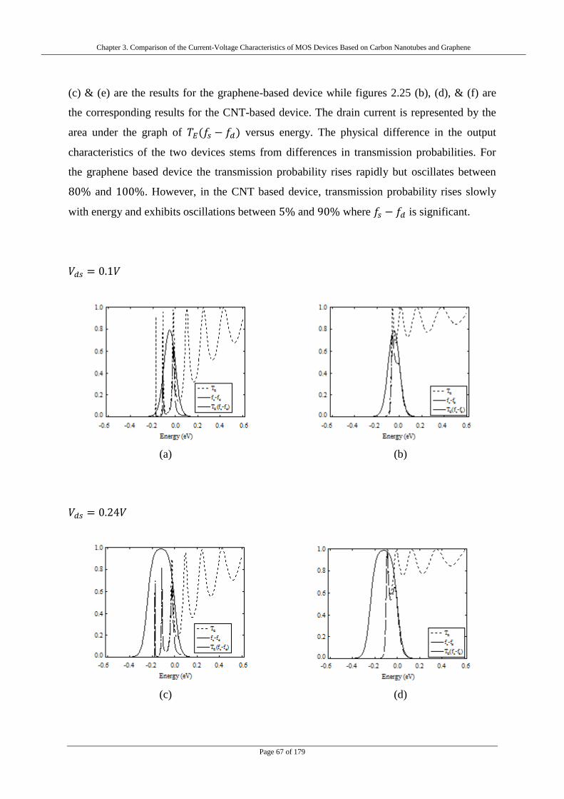
Chapter 3. Comparison of the Current-Voltage Characteristics of MOS Devices Based on Carbon Nanotubes and Graphene
Page 67 of 179
(c) & (e) are the results for the graphene-based device while figures 2.25 (b), (d), & (f) are
the corresponding results for the CNT-based device. The drain current is represented by the
area under the graph of versus energy. The physical difference in the output
characteristics of the two devices stems from differences in transmission probabilities. For
the graphene based device the transmission probability rises rapidly but oscillates between
and . However, in the CNT based device, transmission probability rises slowly
with energy and exhibits oscillations between and where is significant.
(a) (b)
(c) (d)

Chapter 3. Comparison of the Current-Voltage Characteristics of MOS Devices Based on Carbon Nanotubes and Graphene
Page 68 of 179
(e) (f)
Figure 3.6: Transmission Probability and Fermi Dirac Distribution for different . Carbon
nanotubes – (a), (c), (e) and graphene – (b), (d), (f)
As shown in Fig. 3.6, the current increases until the maximum value of is unity.
Beyond that point, the current is mainly determined by while the change in has
no effect on the net current. The plot shows that above the conduction band edge all the
energy states in graphene make a contribution to the current where the transmission
probabilities are well above zero. For a CNT, the transmission probabilities for electrons at
some states are close to zero thereby making little contribution to the current and increasing
the magnitude of required to obtain maximum current.

Chapter 3. Comparison of the Current-Voltage Characteristics of MOS Devices Based on Carbon Nanotubes and Graphene
Page 69 of 179
3.5 Conclusions
In this work charge transport in MOS systems based on graphene nanoribbon and carbon
nanotubes has been modeled and compared. Poisson‟s equation is discretized in three-
dimensions and solved self-consistently with Schrödinger‟s equation. The latter is solved
using the scattering matrix method enabling resonance effects to be taken into account. The
band structure of graphene is obtained through a tight-binding Hamiltonian of the armchair-
edge nanoribbon. To improve immunity to short channel effects, a fully wrapped gate is
assumed for both devices [13].
In the graphene-based FET edge effects influence the energy band structure and charge
density. Differences are observed in the output characteristics of the two devices that stem
from differences in transmission probabilities. For CNFET‟s the transmission probability is
the same at all points on the circumference of the nanotube. However, the structure chosen
for the graphene FET results in potential differences between the edges and the centre of the
graphene sheet leading to differences in the amplitudes of the electron wavefunction. The
total transmission probability for the graphene FET is, therefore, a summation of transmission
probabilities over the width of the graphene nanoribbon. As each element of the summation
has the characteristic form exhibited by the CNT structure the total transmission probability
for the nanoribbon displays smaller oscillations and a more rapid rise in average value with
increasing energy.
The output characteristics of the CNFET and GFET devices are largely dependent on the
contacts used to terminate the device ends. In the next chapter, electron transport in CNTs is
studied using non-contacting means. The contactless studies were carried out on CNTs as
samples are readily available.

Chapter 3. Comparison of the Current-Voltage Characteristics of MOS Devices Based on Carbon Nanotubes and Graphene
Page 70 of 179
3.6 References
[1] J. Guo, S. Datta, M. P. Anantram and M. Lundstrom, Atomistic Simulation of Carbon
Nanotube Field-Effect Transistors Using Non-Equilibrium Green‟s Function
Formalism, Journal of Computational Electronics, Volume 3, Numbers 3-4, 373-377,
2005.
[2] D. L. John, L. C. Castro, P. J. S. Pereira, and D. L. Pulfrey, A Schrodinger-Poisson
Solver for Modeling Carbon Nanotube FETs, Proc. NSTI Nanotech, vol. 3, pp. 65-68,
2004.
[3] M. Pourfath, H. Kosina, and S. Selberherr, A fast and stable Poisson-Schrodinger
solver for the analysis of carbon nanotube transistors, Journal of Computational
Electronics, vol. 5, pp. 155-159, 2006.
[4] R. Saito, G. Dresselhaus, and M. S. Dresselhaus, Physical Properties of Carbon
Nanotubes. London: Imperial College Press, 1998.
[5] K. S. Novoselov, A. K. Geim, S. V. Morozov, D. Jiang, Y. Zhang, S. V. Dubonos, I.
V. Grigorieva, and A. A. Firsov, Electric Field Effect in Atomically Thin Carbon
Films. vol. 306: American Association for the Advancement of Science, 2004, pp.
666-669.
[6] J. Fernandez-Rossier, J. J. Palacios, and L. Brey, Electronic structure of gated
graphene and graphene ribbons, Physical Review B, vol. 75, pp. 205441, 2007.
[7] G. Gu, S. Nie, R. M. Feenstra, R. P. Devaty, W. J. Choyke, W. K. Chan, and M. G.
Kane, Field effect in epitaxial graphene on a silicon carbide substrate, Applied
Physics Letters, vol. 90, pp. 253507-3, 2007.
[8] D. Gunlycke and C. T. White, Tight-binding energy dispersions of armchair-edge
graphene nanostrips, Physical Review B, vol. 77, pp. 115-116, 2008.
[9] J. Charlier, P. C. Eklund, J. Zhu, and A. C. Ferrari, Electron and Phonon Properties of
Graphene: Their Relationship with Carbon Nanotubes, TOPICS IN APPLIED
PHYSICS, vol. 111, pp. 673, 2008.

Chapter 3. Comparison of the Current-Voltage Characteristics of MOS Devices Based on Carbon Nanotubes and Graphene
Page 71 of 179
[10] D. K. Ferry and S. M. Goodnick, Transport in Nanostructures, Cambridge University
Press, 1997.
[11] G. C. Liang, N. Neophytou, D. E. Nikonov, and M. S. Lundstrom, Performance
projections for ballistic graphene nanoribbon field-effect transistors, IEEE
Transactions on Electron Devices, vol. 54, pp. 677-682, Apr 2007.
[12] C. Schonenberger, Bandstructure of Graphene and Carbon Nanotubes: An Exercise in
Condensed Matter Physics, April 2000.
[13] Y. Ouyang, Y. Yoon, and J. Guo, Scaling Behaviors of Graphene Nanoribbon FETs:
A Three-Dimensional Quantum Simulation Study, Electron Devices, IEEE
Transactions on, vol. 54, pp. 2223-2231, 2007.

Chapter 4. Experiment – Contactless Measurements of Electron Transport in Carbon Nanotubes
Page 72 of 179
Chapter 4
Experiment – Contactless Measurements of Electron Transport in Carbon
Nanotubes
4.1 Introduction - Metallic Contact Limitations
There has been intensive research on carbon nanotubes (CNTs) to examine their electron
transport properties and their possible use as future nanoscale devices. So far, experimental
results have shown that these new carbon structures have the potential to be the building
blocks of electronic systems for various applications [1][2].
The electronic properties of CNTs have mostly been observed by connecting electrodes to the
nanotube ends but quantised conductance appears on making contacts [3]. There is a
fundamental ballistic conductance which sets a saturation of the device current with a
quantum resistance. As shown in Fig. 4.1, there is a broadening of the energy level that
accompanies the coupling of the nanotube to the electrodes. As a result, part of the energy
level spreads outside the energy range between electrochemical potentials and where
current flows, consequently reducing the expected current. The ballistic conductance of the
device is expressed as:
(4.1)
where is the device current, is the drain voltage, is the electron charge, is the
reduced Planck‟s constant, and is the coupling strength. In chapter 2, it was observed that

Chapter 4. Experiment – Contactless Measurements of Electron Transport in Carbon Nanotubes
Page 73 of 179
the on-current of a CNFET device depends on the tunnelling barrier, the height of which is
determined by the end contacts.
Figure 4.1: (a) A small drain bias applied across the channel causing a splitting of the
electrochemical potentials. (b) Energy level broadening due to the process of coupling to the
channel.
Experimentally, it is difficult to control the contact effects of the electrodes, which is one of
the issues in the development of CNT devices. So, there is still a need to determine the
fundamental properties of CNTs, accurately.
In this chapter, electron transport in CNTs is studied using non-contacting means, by
inducing current in individual nanotubes using microwave energy. A sample of nanotubes is
inserted into the high field region of a hairpin resonator cavity, and this drives current along
the nanotubes. The electronic properties of the CNTs are then examined using cavity
perturbation theory [4]. In this study, the very nature of current in the sample is specified by
imposing Ohm‟s law to be satisfied within the lossy sample.
In the next section, the experimental techniques used to observe the morphology and
microstructure of the CNTs are introduced.

Chapter 4. Experiment – Contactless Measurements of Electron Transport in Carbon Nanotubes
Page 74 of 179
4.2 Experimental Techniques
Detailed information of the nanotube sample topography is obtained using scanning electron
microscopy (SEM), high-resolution transmission electron microscopy (HRTEM) and energy
dispersive X-ray spectroscopy (EDX). The microstructure of the CNTs is examined using
HRTEM, and the morphology of the sample is examined using SEM. EDX is used on
selected areas of the CNT for composition analysis.
4.2.1 Scanning Electron Microscopy/Transmission Electron Microscopy [5]
A scanning electron microscope images the surface of samples using a high-energy beam of
electrons [5]. Electrons from a field-emission cathode are accelerated through a voltage
difference between the cathode and anode, in the range of and . The smallest
beam cross-section at the gun is demagnified by a two- or three-stage electron lens system so
that an electron probe is formed at the surface of the specimen. Detectors inside the chamber
record the emitted electron spectrum. The emitted electrons interact with the atoms in the
molecule producing signals that contain information about the sample. A deflection coil
system raster scans the electron probe across the specimen in synchronisation with the
electron beam of a separate cathode-ray tube (CRT). One of the signals recorded modulates
the intensity of the CRT to form an image.
Transmission electron microscopy (TEM) is one of the main tools used for observing the
microstructural characterization of materials [6]. A variation in the intensity of electron
diffraction across a thin specimen, known as diffraction contrast, is used for making images
of defects. In HRTEM, the phase of the diffracted electron wave is preserved and allowed to
Chapter 4. Experiment – Contactless Measurements of Electron Transport in Carbon Nanotubes
Page 75 of 179
interfere with the phase of the transmitted wave. The phase contrast imaging technique is
used to form images of columns of atoms. The high-energy electrons in the microscope cause
electronic excitations of the atoms in the specimen and chemical information can be obtained
from the electron excitations.
4.2.2 Energy Dispersive X-ray Spectroscopy [7]
Energy dispersive X-ray spectroscopy is an analytical technique used predominantly for the
elemental analysis of a specimen [7]. X-rays of a variety of energies are generated by the
specimen and strike a silicon crystal. When the X-ray strikes the silicon crystal, it releases its
energy in series of collision events and each event gives rise to one electron and one hole.
Since there is a voltage bias of between the gold layers at the surface of the silicon
crystal, the electrons and holes are attracted to the opposite sides of the crystal, causing a
pulse of current to occur. The energy of the X-ray entering the crystal is proportional to the
number of electron-hole pairs generated. Therefore, the current pulse is also proportional to
the X-ray energy. The generated current pulse is converted to a voltage pulse, and the height
of the voltage pulse is proportional to the energy of the incident X-ray. The pulse height
analyser measures the height of the voltage pulse and stores the result.
The information of the pulse stored after a period is a spectrum, which has as its ordinate the
X-ray energy and its abscissa the number of pulses proportional to the number of X-rays that
entered the silicon crystal of this energy.
In the next section, the morphology and the microstructure of the CNTs sample used for this
experiment are examined. Powdered nanotubes were obtained from Thomas Swan Ltd. The
nanotubes were grown at by thermal chemical vapour decomposition (CVD) on Ni/Si
substrates, giving a mixture of semiconducting and metallic SWNTs.

Chapter 4. Experiment – Contactless Measurements of Electron Transport in Carbon Nanotubes
Page 76 of 179
4.3 Microstructure and Morphology of the CNTs
Using a mortar and pestle, the clumped nanotubes are manually ground, turning them into
fine particles. The surface topography and microstructure were analysed using SEM and
TEM, respectively. A Cu/Rh grid covered with formvar was used for the TEM grid [8].
About of nanotube powder is dispersed in of toluene solvent, followed by an
hour sonication in order to achieve full dispersion, and a drop was deposited on the grid. In
addition, Energy Dispersive X-ray Spectroscopy is used to examine the composition of the
nanotubes sample.
Figure 4.2 shows the SEM image of the nanotubes before and after manual grinding. The
long nanotubes are broken into smaller segments and it is possible to obtain a finer sample.
This confirms the production of short carbon nanotubes, which has been previously reported
using the ball milling technique [8].
(a)

Chapter 4. Experiment – Contactless Measurements of Electron Transport in Carbon Nanotubes
Page 77 of 179
(b)
0.4µm
(c)
Figure 4.2: SEM image of the CNTs used for this experiment (a) before and (b,c) after
manual grinding.
Structural characteristics of the nanotubes were observed by TEM. From TEM observations,
the nanotube length can be measured and the distribution of the nanotubes within the bulk
sample can be examined. Fig. 4.3 shows the TEM images of the nanotubes with diameters
ranging from to and the length ranging from to . Scanning
transmission microscopy (STEM) of the nanotubes shows that there are iron (Fe) impurities
on the surface of the nanotubes. These magnetic impurities are from the substrate used to
stimulate the growth of the nanotubes during production [8]. More TEM images of the
nanotubes are shown in Appendix 7.

Chapter 4. Experiment – Contactless Measurements of Electron Transport in Carbon Nanotubes
Page 78 of 179
(a)
(b)
Figure 4.3: (a) The TEM image of the nanotube sample, the dark spots representing the
impurities and (b) an evidence of the Fe content (inset) in the STEM image of the sample.

Chapter 4. Experiment – Contactless Measurements of Electron Transport in Carbon Nanotubes
Page 79 of 179
The EDX analysis also confirmed the presence of iron (Fe) impurities in the chemical
composition of the nanotubes sample. The volume of contamination is less than 3% of the
entire sample. As shown in Table 4.1, EDX gives atomic % ratios of 96.5:2.7:0.8 for C:O:Fe.
Since the small amount of Fe in the nanotube sample is well dispersed, it is not expected to
influence the microwave measurements.
Figure 4.4: EDX result showing the composition of the CNTs.
Element Weight % Atomic %
Carbon, C 92.99 96.48
Oxygen, O 3.52 2.74
Iron, Fe 3.49 0.78
Totals 100.00 100.00
Table 4.1: Elemental analysis of the nanotubes sample using EDX.
In the next section, the hairpin resonator used to study the electronic properties of the CNTs
is described.

Chapter 4. Experiment – Contactless Measurements of Electron Transport in Carbon Nanotubes
Page 80 of 179
4.4. Copper Hairpin Resonator
A hairpin resonator is equivalent to a quarter wavelength long resonant transverse
electromagnetic transmission line (TL) [9]. A schematic representation of a hairpin resonator
is shown in Fig. 4.5. Microwaves are coupled into the resonator cavity through a pair of loop-
coupled coaxial cables, which induce a standing quarter wave resonance along the hairpin
resonator. A segment of the TL resonates when its length equals odd integer multiples of a
quarter wavelength. The fundamental resonant mode occurs at and its corresponding
resonant frequency is:
(4.2)
where represents the length of the hairpin and is the speed of light. As shown in Fig. 4.5a,
the electromagnetic fields mainly occupy the volume of the parallel plates. There are two
insertion points in the radiation shield of the resonator, top and bottom and correspond to the
electric field maximum and magnetic field maximum, respectively. Samples can be placed in
either the magnetic field or the electric field region depending on the required measurement.
A vector network analyser (VNA) is used to measure the magnitude of the voltage
transmission coefficient of the hairpin resonator as a function of frequency. VNAs are
usually employed for measuring the quality factor and the resonant frequency .

Chapter 4. Experiment – Contactless Measurements of Electron Transport in Carbon Nanotubes
Page 81 of 179
Electric field maximum
Magnetic field maximum
Coupling loops
Radiation Shield
(a)
Magnetic field
Electric field
(b)
d
l
(c)
Figure 4.5: A schematic of the hairpin resonator used for the microwave measurements [9].
(a) Side view (b) Top view and (c) Inner structure.

Chapter 4. Experiment – Contactless Measurements of Electron Transport in Carbon Nanotubes
Page 82 of 179
The quality factor of the resonator is the ratio of the resonant frequency to the frequency of
the bandwidth at half-maximum power . It gives an indication of the overall sensitivity of
the resonator and it should be large enough to show the maximum change in the bandwidth
when a sample is inserted. When the quality factor is high for a small volume of the parallel
plates in the resonator, there is high filling factor when the sample is inserted into the cavity,
leading to a very sensitive measurement. The ideal spectral response of a resonator operating
in the transmission mode is shown in Fig. 4.6.
Frequency (GHz)
Tra
nsm
itte
d P
ow
er (
dB
)
0
3 dB
0f
Bf
1f
2f
Figure 4.6: The spectral response of a resonator in transmission mode observed using the
Agilent E5071B Network Analyser.
The cavity perturbation technique is based on first-order perturbation theory [10], and it is
frequently employed when resonators are modified by the introduction of small samples into
their cavities. The main assumption in the perturbation technique is that and
, where is the permittivity, is the loss factor, and are changes
in and due to sample insertion, respectively [11].

Chapter 4. Experiment – Contactless Measurements of Electron Transport in Carbon Nanotubes
Page 83 of 179
4.5 Experimental Analysis using Cavity Perturbation Technique
In this experiment, a sample of CNTs is inserted in the high magnetic field region of the
hairpin resonator cavity. The electrical properties of the CNTs were then examined using
cavity perturbation technique. Fig. 4.7 shows the hairpin resonator used for this experiment.
The hairpin resonator is treated as a transmission-line antenna that is shorted at one end while
opened at the other end, forming a two-plated hairpin structure [12]. The fundamental
resonant frequency of the hairpin resonator is determined by Eq. 4.2. At resonance, the
electric field is at its maximum at the open circuit end and zero at the short circuit end. On the
other hand, the magnetic field is largest at the short circuit end and zero at the open circuit
end.
The hairpin resonator used in this experiment was constructed from a thick copper
sheet with a length of . According to Eq. 4.2, these dimensions yield a resonant
frequency of . The hairpin structure was enclosed in a copper radiation shield having a
diameter of . The radiation shield ensured that a high was obtained by avoiding the
loss of the stored energy through emission of the electromagnetic radiation.
coaxial
input
20 mm
sample
inserted here
outer
radiation
shield
coaxial
output
magnetic field
distribution
silica tube
containing
sample
l = 23mm
→ f = c/4l = 3 GHz
(a) (b)
Figure 4.7: (a) 3GHz copper hairpin resonator & (b) Inner structure of the resonator.
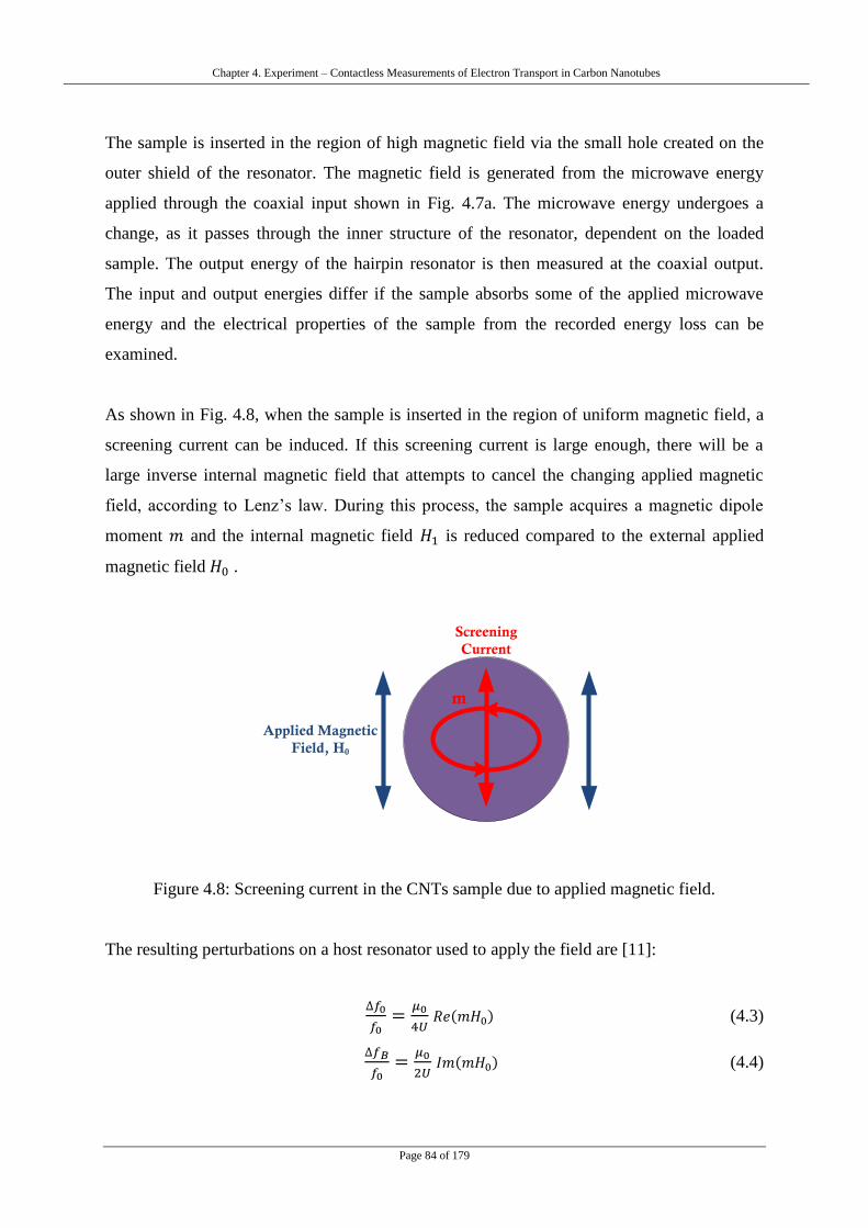
Chapter 4. Experiment – Contactless Measurements of Electron Transport in Carbon Nanotubes
Page 84 of 179
The sample is inserted in the region of high magnetic field via the small hole created on the
outer shield of the resonator. The magnetic field is generated from the microwave energy
applied through the coaxial input shown in Fig. 4.7a. The microwave energy undergoes a
change, as it passes through the inner structure of the resonator, dependent on the loaded
sample. The output energy of the hairpin resonator is then measured at the coaxial output.
The input and output energies differ if the sample absorbs some of the applied microwave
energy and the electrical properties of the sample from the recorded energy loss can be
examined.
As shown in Fig. 4.8, when the sample is inserted in the region of uniform magnetic field, a
screening current can be induced. If this screening current is large enough, there will be a
large inverse internal magnetic field that attempts to cancel the changing applied magnetic
field, according to Lenz‟s law. During this process, the sample acquires a magnetic dipole
moment and the internal magnetic field is reduced compared to the external applied
magnetic field .
Screening
Current
Applied Magnetic
Field, H0
m
Figure 4.8: Screening current in the CNTs sample due to applied magnetic field.
The resulting perturbations on a host resonator used to apply the field are [11]:
(4.3)
(4.4)

Chapter 4. Experiment – Contactless Measurements of Electron Transport in Carbon Nanotubes
Page 85 of 179
where is the magnetic constant, is stored energy, is the increased resonant
frequency, is the increased bandwidth. The total energy stored is the sum of electric
and magnetic energies, which are equal at resonance [13]:
V
m dVHUU 200
2
12
(4.5)
where is the cavity volume and is the stored magnetic energy. As shown in Eq. 4.3 and
Eq. 4.4, the real and imaginary parts of the applied magnetic field are related to the stored
energy and therefore, the electrical properties of the loaded sample can be examined from the
stored energy.
Now, an expression that relates the applied magnetic field to the internal magnetic
field is derived. The magnetic moment and the internal magnetic field depend on the
geometry of the CNTs. Since this varies for different measurements, the analysis is semi-
quantitative.
The screening current is calculated from the generated internal magnetic field. Fig. 4.9 shows
the possible screening current directions in the nanotubes. In the analysis, the individual
nanotube is treated as a conductor and quantisation is ignored, allowing electrons to move
freely along the length of the nanotube.
Figure 4.9: Possible screening current patterns for various orientations of the CNTs in the
bulk sample.

Chapter 4. Experiment – Contactless Measurements of Electron Transport in Carbon Nanotubes
Page 86 of 179
The relationship between the internal magnetic field and the applied magnetic field is
derived for all possible screening current directions in the sample. Fig. 4.10 shows one of the
possible geometries of the nanotubes in the bulk sample. The magnetic moment of the
system measures the strength and the direction of its magnetisation. The relationship between
the magnetic moment and the screening current is given by:
(4.6)
where is the screening current and is the area enclosed by the loop. The magnetisation
is the quantity of magnetic moment per unit volume . In the system, is related to by:
(4.7)
Solving for the internal magnetic field , equating Eq. 4.6 to Eq. 4.7 yields:
(4.8)
z
a
∂z∂l
td
Figure 4.10: One of the possible geometries of the nanotubes in the bulk sample.
According to Faraday‟s law of electromagnetic induction, the induced electric field is related
to the magnetic field by:
(4.9)
(4.10)

Chapter 4. Experiment – Contactless Measurements of Electron Transport in Carbon Nanotubes
Page 87 of 179
(4.11)
(4.12)
where is the radius of the nanotube. The current density is proportional to the electric
field , as expressed by Ohm‟s law:
(4.13)
(4.14)
where is the thickness of the graphene wall of the nanotube, which is around .
Solving Eq. 4.8 and Eq. 4.13 together yields:
(4.15)
(4.16)
where the electrical conductivity , is related to the sheet resistance by:
(4.17)
Substituting Eq. 4.12 into Eq. 4.16, we have
(4.18)
(4.19)
(4.20)
In all three cases described in Fig. 4.9, the internal magnetic field is related to the applied
magnetic field through Eq. 4.21.

Chapter 4. Experiment – Contactless Measurements of Electron Transport in Carbon Nanotubes
Page 88 of 179
(4.21)
From Eq. 4.18, the relaxation time , is defined as:
(4.22)
Based on Eq. 4.21, effective screening only occurs in the limit when . This leads to
the limits on the sheet resistance, which is , as obtained from Eq. 4.22. For the
magnetic field applied to the CNTs sample, the main results are [11]:
(4.23)
(4.24)
where, is the total sample volume, is the effective cavity volume defined via:
22
10 lWddVHHVcavity
eff (4.25)
where , , and are the length, width and diameter of the hairpin, respectively.
The radius of the nanotube sample is much less than the skin depth, and the sample can be
treated as a lossy dielectric with a uniform internal magnetic field responding to the
applied magnetic field . Therefore, the change in the spectral response bandwidth due to
the loaded nanotubes sample is proportional to the conductivity of the sample.
In the next section, the experimental results obtained using the microwave host cavity
to study the electronic properties of single-walled carbon nanotubes (SWNTs) are discussed.

Chapter 4. Experiment – Contactless Measurements of Electron Transport in Carbon Nanotubes
Page 89 of 179
4.6 Experimental Results
The CNTs were dispersed in paraffin wax using by volume powder:wax composite, in a
uniform manner. Samples were loaded into low-loss quartz tubes (inner diameter of
and wall thickness of ) and placed parallel to the magnetic field in the quarter-
wave copper hairpin cavity with magnetic coupling, shown in Fig. 4.7.
The transmitted microwave power was measured in the frequency domain using an Agilent
E5071B network analyser operating in the transmission mode (S21). The spectral response of
the resonator was observed with and without the nanotubes sample. The recorded bandwidth
when the resonator contains an empty quartz tube is subtracted from the recorded bandwidth
when the resonator contains the sample plus quartz tube. The interaction between the
microwave energy and the quartz tube is very small. Therefore, the tube does not affect the
magnetic field in its vicinity.
Fig. 4.11 shows the spectral response of the hairpin resonator when empty. Microwave
energy is transferred into the resonator cavity and the output power, which depends on the
content of the resonator, is measured from the coaxial output. The spectral response plot
shows the transmitted power, which is the ratio of the input and output microwave energy
measured in decibels against frequency in Hertz. The bandwidth , the centre frequency ,
and the quality factor are determined from the spectral response plot. The quality factor of
the empty cavity is around , which is large for its small volume ( ), thus
enhancing the sample filling factor for sensitive measurements.

Chapter 4. Experiment – Contactless Measurements of Electron Transport in Carbon Nanotubes
Page 90 of 179
Figure 4.11: Spectral response of the empty hairpin resonator.
As part of the experimental analysis, a calibration was carried out. Small copper spheres of
radii were inserted into the same magnetic field region of the resonator cavity. As
shown in Fig. 4.12, a frequency shift of per sphere is observed, which
allows comparison of the experimental effective cavity volume of to the
expected value of . The length , width and diameter are ,
and , respectively
.
(a)
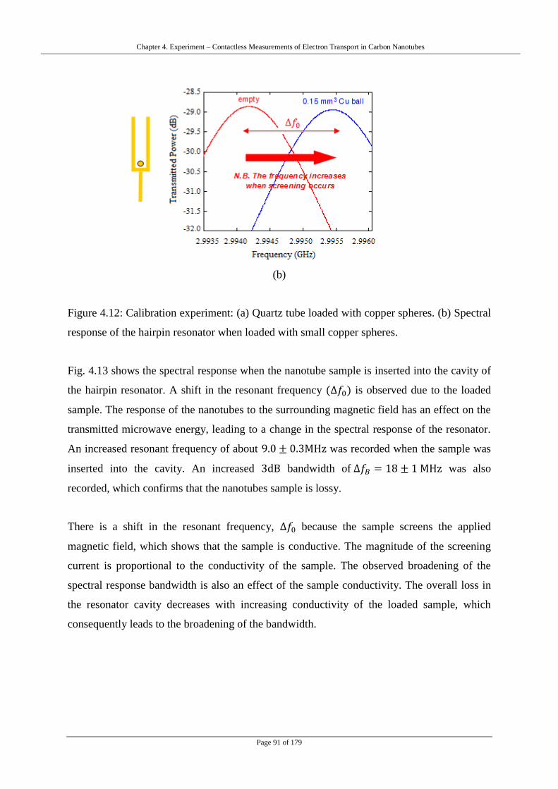
Chapter 4. Experiment – Contactless Measurements of Electron Transport in Carbon Nanotubes
Page 91 of 179
(b)
Figure 4.12: Calibration experiment: (a) Quartz tube loaded with copper spheres. (b) Spectral
response of the hairpin resonator when loaded with small copper spheres.
Fig. 4.13 shows the spectral response when the nanotube sample is inserted into the cavity of
the hairpin resonator. A shift in the resonant frequency is observed due to the loaded
sample. The response of the nanotubes to the surrounding magnetic field has an effect on the
transmitted microwave energy, leading to a change in the spectral response of the resonator.
An increased resonant frequency of about was recorded when the sample was
inserted into the cavity. An increased bandwidth of was also
recorded, which confirms that the nanotubes sample is lossy.
There is a shift in the resonant frequency, because the sample screens the applied
magnetic field, which shows that the sample is conductive. The magnitude of the screening
current is proportional to the conductivity of the sample. The observed broadening of the
spectral response bandwidth is also an effect of the sample conductivity. The overall loss in
the resonator cavity decreases with increasing conductivity of the loaded sample, which
consequently leads to the broadening of the bandwidth.

Chapter 4. Experiment – Contactless Measurements of Electron Transport in Carbon Nanotubes
Page 92 of 179
(a)
(b)
Figure 4.13: (a) Spectral response of the hairpin resonator when loaded with nanotubes
sample, (b) Scaled plot of the spectral response shown in (a).

Chapter 4. Experiment – Contactless Measurements of Electron Transport in Carbon Nanotubes
Page 93 of 179
The observed resonant frequency shift is largely dependent on how the magnetic field is
screened within the nanotubes. From the measurements, the screened volume is
with an estimated nanotube volume of (estimated from
powder mass of ). As shown in Fig. 4.13, the screening current is quite high for such a
small sample mass, which confirms that the conductivity of the CNTs is high. As shown in
Eq. 4.22, an effective screening of the magnetic energy only occurs in the limit when ,
therefore, /sq based on a mean nanotube radius of . Also, based
on the recorded bandwidth increase, the calculated sheet resistance is . Using
Eq. 4.17, the calculated conductivity of an individual CNT is , which is
extremely high.
Fig. 4.14 shows the spectral response of the hairpin resonator when loaded with graphite. A
similar measurement performed on graphite shows that the conductivity of graphite is not
sufficient for measurable screening, justifying the experimental procedure.
Figure 4.14: Resonant traces for graphite powder.

Chapter 4. Experiment – Contactless Measurements of Electron Transport in Carbon Nanotubes
Page 94 of 179
In addition, the sample magnetisation was examined because the nanotube powder attracts
magnets. The magnetisation as a function of the applied magnetic field was measured using a
vector vibrating sample magnetometer [14]. Fig. 4.15 shows the magnetisation versus the
applied magnetic field curves for the nanotubes. The detailed properties of the hysteresis loop
were not included in the analysis because a tiny magnetic signature was observed in the
CNTs sample. The size of the coercive field, saturation fields and the remanences in the
hysteresis loop are too small to analyse.
Figure 4.15: Magnetisation versus applied magnetic field curve for the sample with a mass of
.

Chapter 4. Experiment – Contactless Measurements of Electron Transport in Carbon Nanotubes
Page 95 of 179
4.7 Conclusions
In this work, microwaves have been used as a means of exciting currents in CNTs, thus
avoiding the requirement for electrical contacts. In the experiments, a powder CNT sample is
placed in a region of high microwave magnetic field in a copper hairpin cavity and the
electrical properties of the CNTs are determined using the cavity perturbation technique.
The sample exhibited screening of the microwave magnetic field, that is, an increased
resonant frequency relative to the empty tube, together with very large
losses, that is, an increased bandwidth of . Such screening is usually
observed only in powdered metals having a conductivity large enough for the mean particle
size to become much greater than the microwave skin depth. Based on a mean nanotube
radius of , the recorded nanotube sheet resistance is . An extremely high
conductivity of was estimated from the sheet resistance of individual nanotube.
The nanotubes appear to have the highest conductivity of any non-superconducting material.
The morphology and microstructural studies conducted on the CNTs sample confirmed the
presence of magnetic impurities in the sample. EDX gave atomic % ratios of 96.5:2.7:0.8 for
C:O:Fe. These impurities are thought to arise from the substrate used to stimulate the growth
of the nanotubes during production. Since the small amount of Fe is well dispersed, it is not
expected to influence the microwave measurements significantly.
Since the properties of CNTs are very sensitive to their geometries, the applied magnetic field
could have changed their internal structures, thus causing the magnetic signatures in the
CNTs. This work is inconclusive because not all samples examined show such striking
behaviour, so future work should consider experimenting on wider range of frequencies and
on well-aligned nanotubes.
Chapter 4. Experiment – Contactless Measurements of Electron Transport in Carbon Nanotubes
Page 96 of 179
4.8 References
[1] N. Patil, J. Deng, S. Mitra, and H. S. Philip Wong, Circuit-Level Performance
Benchmarking and Scalability Analysis of Carbon Nanotube Transistor Circuits,
IEEE Transactions on Nanotechnology, Vol. 8, No. 1, January 2009.
[2] G. F. Close, S. Yasuda, B. Paul, S. Fujita, and H. S. Philip Wong, A 1 GHz Integrated
Circuit with Carbon Nanotube Interconnects and Silicon Transistors, Nano Lett.,
2008, 8 (2), pp. 706–709.
[3] M. P. Anantram and F. Leonard, Physics of Carbon Nanotube Electronic Devices,
Institute of Physics Publishing, Rep. Prog. Phys. 69 (2006), pp. 507-561.
[4] D. M. Pozar, Microwave Engineering, 3rd
Edition, Page 266, John Wiley & Sons, Inc.,
ISBN: 978-0-471-44878-5, 2005.
[5] L. Reimer, T. Tamir, A. L. Schawlow, Scanning Electron Microscopy: Physics Of
Image Formation and Microanalysis Mark, 2nd
Edition, Springer Berlin Heidelberg,
ISBN: 3540639764, 1998.
[6] B. Fultz, J. M. Howe, Transmission electron microscopy and diffractometry of
materials, 3rd
Edition, Springer, ISBN: 3540738851, 2007
[7] G. H Bourne, J. F. Danielli, International Review of Cytology: A Survey of Cell
Biology, volume 58, Academic Press, ISBN-10 / ASIN: 0123643589, 1979.
[8] N. Pierard, A. Fonseca, Z. Konya, I. Willems, G. Van Tendeloo and J. B.Nagy,
Production of short carbon nanotubes with open tips by ball milling, Chemical
Physics Letters 335 (2001) 1-8.
[9] P. A. Anderson, A. R. Armstrong, P. D. Barkera, M. J. Edmondson, P. P. Edwards
and A. Porch, Rubidium doped zeolite rho: structure and microwave conductivity of a
metallic zeolite, Dalton Transactions, DOI: 10.1039/b402668c, July 2004.
[10] A. P. Gregory and R. N. Clarke, A Review of RF and Microwave Techniques for
Dielectric Measurements on Polar Liquids, IEEE Transactions on Dielectrics and
Electrical Insulation, Vol. 13, No. 4, pp. 727-743, August 2006.
[11] A. Porch, Private Communications, 2007-2008.

Chapter 4. Experiment – Contactless Measurements of Electron Transport in Carbon Nanotubes
Page 97 of 179
[12] B. L. Sands, N. S. Siefert, and B. N. Ganguly, Design and measurement
considerations of hairpin resonator probes for determining electron number density in
collisional plasmas, IOP Publishing, Plasma Sources Sci. Technol. 16 (2007), pp.
716–725.
[13] D. Kajfez and P. Guillon (Editors), Dielectric Resonators, Second Edition, Noble
Publishing Corporation, Atlanta, 1998, ISBN 1-884932-05-3.
[14] B. C. Dodrill, J. R. Lindemuth, and J. K. Krause, Magnetic Anisotropy:
Measurements with a Vector Vibrating Sample Magnetometer, Lake Shore
Cryotronics, Inc., 575 McCorkle Blvd., Westerville, Ohio, USA.

Chapter 5. 3D Electromagnetic Simulation of Hairpin Resonator for the Microwave Characterisation of Carbon Nanotubes Sample
Page 98 of 179
Chapter 5
3D Electromagnetic Simulation of Hairpin Resonator for the Microwave
Characterisation of Carbon Nanotubes Sample
5.1 Introduction
A 3D modelling of the characterisation of tightly packed nanotubes using a hairpin resonator
is now described. The hairpin resonator is modelled using the COMSOL multiphysics
software. It is examined how the presence of nanotubes can change the magnitude of the
magnetic field screening in the hairpin resonator. The magnetic field screening is examined
from the shift in the resonant frequency of the hairpin resonator by introducing different
conductivities. Also, the broadening of the spectral response bandwidth of the hairpin
resonator when the nanotubes are introduced into the cavity is examined. As part of the
analysis, the of the hairpin resonator is calculated from the simulation and its value
compared with that obtained from experiment.
In this simulation, COMSOL serves to solve a complex Helmholtz equation. The Helmholtz
equation relates the amplitude of the magnetic potential to the electrical conductivity of the
measurement sample. The partial differential equation (PDE) that describes the
electromagnetic system is formulated, and the solution of this PDE used to examine the
properties of the nanotubes sample. More detailed information of the COMSOL software is
provided in the following section.

Chapter 5. 3D Electromagnetic Simulation of Hairpin Resonator for the Microwave Characterisation of Carbon Nanotubes Sample
Page 99 of 179
5.2 Background
COMSOL multiphysics [1] is a finite element analysis software used for the modeling and
simulation of any physics-based system. The original COMSOL codes were written by
graduate students for a graduate course at the Royal Institute of Technology in Stockholm,
Sweden [1]. The COMSOL multiphysics modelling environment has a functionality
optimised for the analysis of electromagnetic effects, components and systems. The
underlying equations for electromagnetics are available in all the application modes, which is
a feature unique to COMSOL multiphysics. Any model developed using the electromagnetic
module can be transformed into a model described by the underlying partial differential
equations. Simulation models can be exported to COMSOL script and MATLAB. Also, it is
possible to incorporate the models with other products in the MATLAB family such as
Simulink.
In COMSOL, the finite element method approximates the solution within each element using
some elementary shape function, which can be constant, linear, or of higher order. The mesh
for the problem must be generated before it can be solved, and the requirement for a finer or
coarser mesh depends on the element order in the model. The mesh resolution is determined
by the variation in the solution, which could be due to geometrical factors, skin effect, or
wavelength.
Also, the COMSOL package is equipped with an option to make a selection from a set of
solvers for PDE-based problems. The selection of the solver type is dependent on the
application mode and the analysis type, which includes stationary, eigenfrequency, transient,
time-dependent, and parametric analyses. The simulation results obtained from the solver are
analysed using the postprocessing and visualization tools, which include advanced graphics,
data display and export functions. From the postprocessing tool, the solutions of the
electromagnetic problem such as the field patterns, resonant frequency, and the quality
factor, can be retrieved. It is possible to undertake further postprocessing calculations by
exporting the solutions to MATLAB.
The later sections discuss the detailed modeling and postprocessing of the hairpin resonator.

Chapter 5. 3D Electromagnetic Simulation of Hairpin Resonator for the Microwave Characterisation of Carbon Nanotubes Sample
Page 100 of 179
5.2.1 Theory of COMSOL Multiphysics [4]
In this work, the AC Power Electromagnetics mode is employed for the electromagnetic
simulation of the hairpin resonator. COMSOL computes the PDE coefficients based on the
parameters of the application mode [2].
The PDE for this application mode is formulated by deriving the equation this mode solves,
starting with the Ampere‟s law [3]:
(5.1)
where is the magnetic field intensity, is the electric current density, is the electric flux
density, is the electric field intensity, is the velocity of the conductor and is the
magnetic flux density. Assuming time-harmonic fields and using the potentials yields:
(5.2)
(5.3)
Combining Eq. 5.2 and Eq. 5.3 with the constitutive relationships and
, the Ampere‟s law is rewritten as
(5.4)
where is the electrical conductivity, is the angular frequency, is the magnetic vector
potential, M is the magnetisation and P is the polarisation density.
The following boundary and interface conditions are applied to the electromagnetic problem.
The interface condition is [2]:
(5.5)

Chapter 5. 3D Electromagnetic Simulation of Hairpin Resonator for the Microwave Characterisation of Carbon Nanotubes Sample
Page 101 of 179
The magnetic field boundary condition that specifies the tangential component of the
magnetic field strength at the boundary is:
(5.6)
In addition, specify the surface current flowing along the longitudinal direction ( -direction)
and the surface-current boundary condition:
(5.7)
The electric insulation boundary condition sets the magnetic field to zero:
(5.8)
The magnetic potential boundary condition that specifies the magnetic potential is given by:
(5.9)
The magnetic insulation boundary condition that sets the magnetic potential to zero at the
boundary is:
(5.10)
The continuity boundary condition that allows the continuity of the tangential component of
the magnetic field is:
(5.11)
A solution to an AC power electromagnetic problem is required for a conductor carrying
alternating currents [3]. Consider a homogenous dielectric with a dielectric constant and
magnetic permeability , and it is assumed that there is no charge at any point. The fields
must satisfy a set of Maxwell equations:

Chapter 5. 3D Electromagnetic Simulation of Hairpin Resonator for the Microwave Characterisation of Carbon Nanotubes Sample
Page 102 of 179
(5.12)
(5.13)
where is the electric field, is the magnetic field and is the current density. When there
is no current, the magnetic field can be eliminated from the second set and both fields
satisfy wave equations with wave speed :
(5.14)
–
(5.15)
–
(5.16)
For the charge-free homogenous dielectric with conductivity , the current density is:
(5.17)
The ohmic resistance damps the waves, leading to Eq. 5.18 & Eq. 5.19.
–
–
(5.18)
–
–
(5.19)
Using the complex form, the case of time-harmonic field is treated by replacing with .
The conductivity is calculated using Eq. 5.18 & 5.19, and it can be used to examine the skin
effect and other properties of the current-carrying conductor.
Before solving a radio frequency (RF) cavity problem, the cavity layout must be described in
such a way that it can be utilized as input for solution of the Helmholtz equation. Given a
source-free, linear, isotropic, homogenous region, the Maxwell-Curl equations [4] that
constitute two equations for the two unknowns, and in phasor form are:

Chapter 5. 3D Electromagnetic Simulation of Hairpin Resonator for the Microwave Characterisation of Carbon Nanotubes Sample
Page 103 of 179
(5.20)
(5.21)
Solve Eq. 5.20 and Eq. 5.21 for either or by taking the Curl of these equations to yield:
(5.22)
Eq. 5.22 is simplified using the vector identity , which is valid
for the rectangular components of an arbitrary vector . Since in a source-free
region,
(5.23)
Eq. 5.23 is known as the wave equation or Helmholtz equation for . Derive an identical
equation for using the same steps:
(5.24)
Using the AC Power Electromagnetics mode [5], the equation solved in COMSOL is a
complex Helmholtz equation for the amplitude of the magnetic potential:
(5.25)
(5.26)
The boundary conditions are considered carefully, and either the magnetic potential or the
normal derivative of the same field is specified on the outer surface. The final solution of the
AC Power Electromagnetics equation is a complex value that reflects the time lag between
the surface and the interior.

Chapter 5. 3D Electromagnetic Simulation of Hairpin Resonator for the Microwave Characterisation of Carbon Nanotubes Sample
Page 104 of 179
5.2.2 Skin Depth
The skin effect is observed during the flow of an alternating current. Electrons tend to move
along the surface of the conductor and the current density near the surface of the conductor is
greater than that at its core. A change in the amplitude and direction of the current induces a
magnetic field that pushes electrons towards the exterior of the conductor. As shown in Eq.
5.28, the skin depth increases when the applied frequency decreases. In an infinitely thick
plane conductor, the current density decreases exponentially with depth from the surface,
yielding [6]:
(5.27)
where is the skin depth. The skin depth, also known as the characteristic depth of
penetration, is defined as
(5.28)
where is the frequency, is the conductivity, is the permeability of free space and is
the angular frequency. The skin depth of the conductor is the depth at which the current
density reduces in magnitude to or .
Skin depth plays an important role when investigating screening in a conducting sample. The
radius of the conducting sample must be larger than the skin depth for screening to be
observed.
Since conductivity of the sample is an input parameter in this simulation, the average
conductivity of a CNT is now derived starting from the density of states calculation.

Chapter 5. 3D Electromagnetic Simulation of Hairpin Resonator for the Microwave Characterisation of Carbon Nanotubes Sample
Page 105 of 179
5.2.3 Calculation of the Charge Density in a Carbon Nanotube
In chapter 4, it was reported that the resonant frequency of a hairpin resonator increased
when a sample of carbon nanotubes (CNTs) was placed in the magnetic field anti-node of the
resonator cavity. The resonant frequency increased because the sample screened the
microwave magnetic field. It was also observed that the resonant frequency increased when
small copper spheres were inserted into the hairpin cavity. According to the experimental
analyses in section 4.6, the nanotubes served to screen the microwave magnetic field more
than the copper spheres. This is remarkable as copper (Cu) is known to have a very high
conductivity but the experimental results suggest that the conductivity of a CNT is higher.
Consider a comparison of a CNT to a copper wire. The physical dimensions of the structures
are shown in Fig. 5.1.
(a)
L=1µm
2a=3nm
(b)
Figure 5.1: Cylindrical geometry of (a) carbon nanotube, and (b) copper wire.
For both structures shown in Fig. 5.1, the length and radius are and , respectively.
The charge density in the CNT is compared to that of copper wire using fundamental
calculations. Since the structures are treated as conductors and quantisation ignored, classical
calculations can be used to describe the movement of electrons along their lengths. The
electron concentration in copper is but only the free electrons are included in

Chapter 5. 3D Electromagnetic Simulation of Hairpin Resonator for the Microwave Characterisation of Carbon Nanotubes Sample
Page 106 of 179
this calculation. The free electrons occupy the lowest energy states and they form a sphere in
momentum space [7]. Fig. 5.2 shows the surface of the sphere also known as the Fermi
surface. The free electrons that contribute to current flow are those near the Fermi surface,
and it is assumed that they are below the Fermi energy, where is Boltzmann‟s
constant and T is the absolute temperature [7].
kz
ky
kx
Fermi
Surface
Figure 5.2: The representation of the Fermi surface in momentum space [7].
The radius of the Fermi sphere (red) and the inner sphere (yellow) shown in Fig. 5.2 are
expressed in Eq. 5.29 and Eq. 5.30, respectively [7].
(5.29)
(5.30)
where is the Fermi energy of copper, is the reduced Planck‟s constant and is the
electron mass. In order to determine the number of free electrons in copper, the ratio of the
volume of the Fermi sphere to the volume of the inner sphere is calculated, yielding:
(5.31)

Chapter 5. 3D Electromagnetic Simulation of Hairpin Resonator for the Microwave Characterisation of Carbon Nanotubes Sample
Page 107 of 179
Based on the expression shown in Eq. 5.31 and applying of , the calculated ratio is
0.0056. Therefore, the number of free electrons in copper is the known number of electrons
divided by 178, which is the inverse of the calculated ratio.
The charge density per unit length, , in the copper wire is given by:
(5.32)
where is the number of free electrons per cubic meter and is the cross-sectional area of
the copper wire. From Eq. 5.32, the charge density in the copper wire is .
To calculate the charge density in the CNT, start from the density of states calculation [8].
The density of states for the CNT is determined using Eq. 5.33.
(5.33)
(5.34)
where is the nanotube length, is the diameter, , is the carbon-carbon length,
is an index of the CNT, is the energy subband index, is energy , and is the tight-
binding overlap integral. Fig. 5.3 shows the plot of the density of states for the CNT
considered. The charge density in the CNT structure is related to and the Fermi-Dirac
distribution by:
(5.35)
Performing the integration described in Eq. 5.35 over all possible energies, the charge density
in the CNT structure is . An atom density of is estimated using the
formula shown in Eq. 2.25 (section 2.1.2). These separate calculations point to similar
number of atoms contributing to the conducting “cloud”.

Chapter 5. 3D Electromagnetic Simulation of Hairpin Resonator for the Microwave Characterisation of Carbon Nanotubes Sample
Page 108 of 179
Figure 5.3: Density of states for a carbon nanotube calculated using Eq. 5.33.
Since the conductivity of copper is known to be [7], the conductivity of the
nanotube can be estimated using Eq. 5.37. Conductivity is related to the number of electrons
in the structure and Fermi velocity of charge carriers as:
(5.36)
The charge carried by electrons in the structures shown in Fig. 5.1 is , which is
related to conductivity as:
(5.37)
where is the Fermi velocity and is the electron charge. Using Eq. 5.37, the conductivity of
an individual nanotube is estimated to be , which is lower than that of copper.
This conductivity is significantly different from that extracted from of the hairpin
resonator described in chapter 4, where a conductivity of around was obtained
from the experiment.
The detailed 3D modelling of microwave characterization of CNTs sample using hairpin
resonator is now discussed. This enables validation of the experimental results discussed in
chapter 4. The average conductivity of the nanotubes derived is an input parameter in this
simulation.

Chapter 5. 3D Electromagnetic Simulation of Hairpin Resonator for the Microwave Characterisation of Carbon Nanotubes Sample
Page 109 of 179
5.3 Modelling of Hairpin Resonator
5.3.1 Introduction
In this section, the 3D modelling of the hairpin resonator used to investigate the screening
properties of nanotubes sample is presented. The fundamental theory of a hairpin resonator
was introduced in section 4.4. The hairpin resonator is a variant of the wide microstrip line,
which supports transverse electromagnetic waves (TEM) along its length [9]. The hairpin
structure is made out of a copper strip bent at one end to form the short-circuited termination
while open at the other end. Resonance occurs when the length, of the hairpin is integer
multiples of a quarter wavelength. The fundamental resonance mode occurs at with
the corresponding resonant frequency, given by [9][10]:
(5.38)
As shown in Eq. 5.38, the resonant frequency, of the hairpin resonator only depends on .
Fig. 5.4 shows a schematic diagram of the hairpin resonator considered in this work.
lt
d W
Region of high
electric field
Region of high
magnetic field
Figure 5.4: Schematics of the hairpin resonator, where is the plate length, is the plate
width, is the separation between the plates and is the plate thickness [9][11].

Chapter 5. 3D Electromagnetic Simulation of Hairpin Resonator for the Microwave Characterisation of Carbon Nanotubes Sample
Page 110 of 179
When the hairpin resonates, the electric and magnetic fields increase drastically and a
standing wave occurs on the hairpin such that the voltage (current) is maximum (minimum)
at the open circuit end and minimum (maximum) at the short circuit end. As illustrated in Fig.
5.4, the electric field along the length of the hairpin is concentrated at the open circuit end
and zero at the short circuit end. The magnetic field is largest at the short circuit end and
minimal at the open circuit end. In this work, the concentrated magnetic field is used to
induce current in a tightly packed sample of carbon nanotubes.
The quality factor, is another parameter relevant to the studies in this chapter. The
unloaded quality factor, of the hairpin resonator is derived starting with the transmission
line (TL) resonator [9][10]. As shown in Eq. 5.39, the of transmission line resonators has
two components ( and ):
(5.39)
(5.40)
(5.41)
where is the attenuation constant due to conductor loss, is the attenuation constant due
to dielectric loss, is the skin depth of copper, is the conductor quality factor and is
the dielectric quality factor. Since the spacing between the plates of the hairpin structure is
filled with air, and becomes infinitely large. Therefore, the unloaded
quality factor of the hairpin resonator is only dependent on .
(5.42)
The attenuation constant due to conductor loss, is related to the hairpin resistance and
characteristic impedance as:
(5.43)
(5.44)

Chapter 5. 3D Electromagnetic Simulation of Hairpin Resonator for the Microwave Characterisation of Carbon Nanotubes Sample
Page 111 of 179
The inductance and capacitance are related to the hairpin structure as:
(5.45)
(5.46)
Substituting the equations for and into Eq. 5.44 yields
(5.47)
The hairpin resistance per unit length is given by [9][10]:
(5.48)
where is the resistivity, surface resistance, and is the area of each hairpin
plate. Substituting Eq. 5.47 and Eq. 5.48 into Eq. 5.43 yields:
(5.49)
(5.50)
Applying and into Eq. 5.50, the of the hairpin resonator
becomes:
(5.51)
The relationship between the loaded quality factor, of the resonator and is given by
[12]:
(5.52)
where is the insertion loss.

Chapter 5. 3D Electromagnetic Simulation of Hairpin Resonator for the Microwave Characterisation of Carbon Nanotubes Sample
Page 112 of 179
In the next section, the hairpin resonator is modelled to give a resonance frequency of .
The field patterns, resonant frequency and the quality factor are obtained directly from the
output file of the COMSOL software.
5.3.2 Hairpin Resonator Model
The electromagnetic simulation of the hairpin resonator used for observing screening in
CNTs is now described. The simulation is performed using COMSOL Multiphysics. Fig. 5.5
shows the 3D structure of the hairpin resonator used in this work. The hairpin is constructed
from a thick copper sheet with length , width , and diameter
. Based on these dimensions, the resonant frequency, of the hairpin resonator
is . The hairpin structure is enclosed in a radiation shield made out of copper. As shown
in Fig. 5.5, the radiation shield has two parts; the cylindrical housing surrounding the hairpin
and the base for the cylindrical housing fitting. The radiation shield prevents the loss of
stored energy to the surroundings, ensuring high quality factor.
Figure 5.5: 3D geometry of the hairpin resonator modelled using COMSOL Multiphysics.

Chapter 5. 3D Electromagnetic Simulation of Hairpin Resonator for the Microwave Characterisation of Carbon Nanotubes Sample
Page 113 of 179
Different regions of the resonator are defined in the subdomain settings of COMSOL by
stating the properties of the material such as permittivity and permeability. In the boundary
settings function, the boundary conditions described in section 5.2.1 are applied. At the
interface between two different media, the continuity boundary condition shown in Eq. 5.11
is applied.
In order to reduce the size of the cavity problem and achieve a converged solution, only one
half of the problem geometry is specified as shown in Fig. 5.6. The „create composite object‟
function was used to cut the hairpin resonator model in half. An efficient boundary condition
is then applied on the truncated section of the geometry to minimize the problem size.
Figure 5.6: 3D geometry of the hairpin resonator cut in half to reduce the size of the RF
cavity problem.
The mesh for the hairpin structure to be analysed is set before solving the Helmholtz equation
(Eq. 5.25) that describes the RF cavity problem. A finer mesh is applied where the
electromagnetic field is highly concentrated, which aids the solution convergence. The

Chapter 5. 3D Electromagnetic Simulation of Hairpin Resonator for the Microwave Characterisation of Carbon Nanotubes Sample
Page 114 of 179
eigenfrequency solver is used to obtain and of the hairpin resonator. In this case,
COMSOL computes the solutions of the transverse electric mode to obtain the field
patterns, and they are stored in the post-processing tool of COMSOL. This allows
interpolation of the fields at various points to compute other quantities such as conductor
losses, energy stored within the cavity and screening.
5.3.3 Simulation Results
The 3D simulation of the hairpin resonator using the RF module in COMSOL is now
presented. In the 3D solid shown in Fig. 5.6, the -axis, -axis and -axis represent the
positions along the width, radius and length of the hairpin resonator, respectively. Fig. 5.7a
and Fig. 5.7b show the streamline and contour plot of the magnetic field and electric field in
the empty hairpin resonator, respectively. As expected the magnetic field is concentrated at
the short-circuited end of the hairpin while the electric field is largest at the open end of the
hairpin. As depicted by the bar in Fig. 5.7, the maximum magnetic field strength is around
while the maximum electric field is around .
(a)

Chapter 5. 3D Electromagnetic Simulation of Hairpin Resonator for the Microwave Characterisation of Carbon Nanotubes Sample
Page 115 of 179
(b)
Figure 5.7: Field concentration and distribution within the hairpin. (a) High magnetic field
concentration observed at the short-circuited end of the hairpin. (b) Electric field is maximum
at the open end of the hairpin.
Figure 5.8: Top view of the magnetic field pattern within the radiation shield of the hairpin
resonator.

Chapter 5. 3D Electromagnetic Simulation of Hairpin Resonator for the Microwave Characterisation of Carbon Nanotubes Sample
Page 116 of 179
In COMSOL the resonant frequency, is computed by numerically integrating the field
components at various points. Based on the simulation results, the resonance frequency of the
empty hairpin resonator is , which is very close to the value recorded in
the experiment using a network analyzer. The of the empty hairpin resonator obtained
from the simulation is 1399, and the corresponding value calculated using Eq. 5.52 is
1220. A value similar to the 1200 recorded in the experiment was obtained.
As shown in Fig. 5.9 the sample of nanotubes is introduced in the high magnetic field region
of the hairpin structure. The nanotubes sample had a packing density of and a
conductivity of , estimated in section 5.1. As shown in Fig. 5.7 and Fig. 5.9,
there is no obvious change in the magnetic field strength when the sample is introduced into
the resonator cavity. The maximum magnetic field strength only reduced from
to because the sample absorbed some of the field.
Figure 5.9: The hairpin resonator is loaded with tightly packed nanotubes sample ( in
volume corresponding to a sample mass of ).

Chapter 5. 3D Electromagnetic Simulation of Hairpin Resonator for the Microwave Characterisation of Carbon Nanotubes Sample
Page 117 of 179
Furthermore, based on the results shown in Table 5.1, there is no significant change in
when the conductivity of the sample is , implying the conductivity is not high
enough to screen the field. The magnitude of field screening is examined from the change in
the resonant frequency of the hairpin resonator by introducing materials with different
conductivities. Table 5.1 shows the trend of the field screening as the conductivity of the
sample increases. The simulation result confirms that increases as the conductivity of the
sample increases. Screening was only observed when the conductivity of the sample is higher
than .
A conductivity of was found in the experiment, therefore computation of was
conducted for this conductivity. A value of was observed, which is similar to
that of the experiment, and validates the simulation procedure.
In addition, a validation of the simulation has been carried out by introducing copper into the
resonator cavity. As discussed in chapter 4, a resonant frequency shift of was
observed on insertion of copper spheres ( ) into the cavity. A similar
scenario has been confirmed in the COMSOL simulation by inserting a copper rod into the
resonator cavity, which results in a resonant frequency shift of . This confirms that
the simulation result is nearly the same as that of the experiment with an error of .
Conductivity (S/m) Resonant Frequency (Hz)
3001417305 908 794
3005485516 1181 1032
3008674750 1327 1160
3010474929 1372 1199
3011215490 1391 1216
3012371644 1394 1218
3019527680 1398 1220
Table 5.1: Recorded increase in the resonant frequency as the conductivity of the nanotubes
sample increases.

Chapter 5. 3D Electromagnetic Simulation of Hairpin Resonator for the Microwave Characterisation of Carbon Nanotubes Sample
Page 118 of 179
Also, the quality factor, was computed when the nanotubes sample is in the hairpin
resonator cavity. The field components are extracted from the COMSOL output file and a
numerical integration was performed to obtain the parameters required for the hairpin
resonator calculations (Eq. 5.52).
For an empty resonator, the value of is 1220 but when a sample of nanotubes having a
conductivity of is inside the region of high magnetic field, the value of
reduces to 1160. There is a reduction in the value of because the sample absorbed some of
the microwave energy. The sample of nanotubes introduced some loss in the resonant device,
which is evident from the value.
The value was used to calculate the change in the spectral response bandwidth from
the well-known factor expression, . The bandwidth increased by
because of the microwave loss introduced by the nanotubes. The sample decreased the overall
loss of the resonator, leading to bandwidth broadening.
In this simulation, similar have been observed when compared to that of the experiment
but there is difference in . In the experiment, was found to be while that
recorded in this simulation is only . This suggests that there is something else
contributing to the experimental observations.
In the following section, quantization in CNTs and the effect of axial magnetic fields on their
electronic structure are discussed.

Chapter 5. 3D Electromagnetic Simulation of Hairpin Resonator for the Microwave Characterisation of Carbon Nanotubes Sample
Page 119 of 179
5.4 Discussion
In a CNT, the electron wave number perpendicular to the axis of the CNT, , is quantized.
The quantized are determined by the boundary condition shown in Eq. 5.53 [13].
(5.53)
where is an integer and is the nanotube diameter. Fig. 5.10 shows the quantization of
wave-states around a CNT. As shown in Fig. 5.10, there is a significant spacing between the
quantised values of for CNTs with small diameters (~ ). Fig. 5.10b shows the contour
plot of graphene valence states for a CNT. The parallel lines represent the wavevectors
allowed in the cylindrical boundary condition, and each line is a 1D subband. Electrons are
free to move over long distances when the electron wave number is continuous.
(a)

Chapter 5. 3D Electromagnetic Simulation of Hairpin Resonator for the Microwave Characterisation of Carbon Nanotubes Sample
Page 120 of 179
(b)
Figure 5.10: Quantization of electronic wave states around a carbon nanotube. (a) The
parallel and perpendicular axes of a CNT. (b) The contour plot of graphene valence states for
a CNT [13].
For a CNT with large diameter, the spacing between the values of are small, which may
lead to continuum of states. In such case, electrons could travel in the circumferential
direction of the CNT as shown in Fig. 5.11. Since some of the CNTs in the experimental
sample have diameters much larger than , electrons travelling in the circumferential
directions can acquire magnetic moments, and consequently screen the surrounding magnetic
field.
Figure 5.11: Screening currents for the microwave magnetic field applied parallel to the
nanotube axis.

Chapter 5. 3D Electromagnetic Simulation of Hairpin Resonator for the Microwave Characterisation of Carbon Nanotubes Sample
Page 121 of 179
When a magnetic field is applied parallel to a CNT, the allowed states in the CNT are
modified by an Aharonov-Bohm phase [13]. In the presence of an axial magnetic field, the
boundary condition for electron wave states around the CNT is given by:
(5.54)
(5.55)
where is the flux passing through the CNT, is the axial magnetic field, and is
the flux quantum. The second term in Eq. 5.54 is the Aharonov-Bohm phase acquired by the
electrons as they encircle a magnetic flux. The allowed states is shifted by an amount
, which consequently changes the bandgap of the CNT. The change in the
bandgap of the CNT is given by [13][14]:
(5.56)
where is the energy bandgap, is the reduced Planck‟s constant, is the Fermi
velocity and the quantity, is the orbital magnetic moment. Electronic states
near the energy gap are predicted [14][15] to have an orbital magnetic moment much larger
than Bohr magneton, which is the magnetic moment due to an electron spin. This large
moment is thought to cause the magnetic behaviour of CNTs [16][17].

Chapter 5. 3D Electromagnetic Simulation of Hairpin Resonator for the Microwave Characterisation of Carbon Nanotubes Sample
Page 122 of 179
5.5 Conclusions
In this chapter, the 3D modelling of tightly packed carbon nanotubes using a hairpin
resonator was described. The conductivity of the sample is one of the input parameters of this
simulation. An expression for the average conductivity of the CNTs was derived starting
from the density of states calculations. Based on the calculations described in section 5.1, the
conductivity used in the simulation is .
For a conductivity of , the resonant frequency of the hairpin decreases
by . An incremental shift was observed in the resonant frequency of the hairpin
resonator only when a sample of highly conductive nanotubes is inside its cavity. In
such a case, the resonant frequency increased because the sample screened the applied
microwave energy. As shown in Table 5.1, there is a trend in as the conductivity of the
sample is varied incrementally. Also, the screening properties of the sample were observed
when its conductivity is (based on the value extracted from the experimental
results). The resonant frequency increased from 3.009GHz to 3.090GHz, which is
comparable to that recorded in the experiment.
In addition, it was examined how changes when the hairpin cavity is loaded with the
nanotubes sample. The value reduces from 1220 to 1160 due to the microwave loss
introduced by the sample in the resonant device. The broadening of the spectral response
bandwidth (i.e. ) is also due to the sample loss.
In the simulations, a resonant frequency shift was observed only when the sample inside the
cavity has a high conductivity ( ). This observation suggests that the nanotubes
used in the experiment have extremely low sheet resistance.

Chapter 5. 3D Electromagnetic Simulation of Hairpin Resonator for the Microwave Characterisation of Carbon Nanotubes Sample
Page 123 of 179
5.6 References
[1] COMSOL Multiphysics, Model Library, COMSOL Multiphysics Version 3.2,
September 2005.
[2] COMSOL Multiphysics Modelling Guide by COMSOL AB, Version 3.2, Application
Modes, Page 2.
[3] COMSOL Multiphysics Modelling Guide by COMSOL AB, Version 3.2, AC Power
Electromagnetics Page(s): 96-99.
[4] M. N.O. Sadiku, Numerical Techniques in Electromagnetics, Wave Equations Page 8,
CRC Press, Boca Raton, 1992.
[5] COMSOL Multiphysics Model Library by COMSOL AB, Version 3.2, Skin Effect in
a Conductor Page(s): 72-79.
[6] Electromagnetics Module, COMSOL Multiphysics User‟s Guide by COMSOL AB,
Version 3.2, Skin Depth Page(s): 172-190.
[7] N. W. Ashcroft, N. David Mermin, Solid State Physics, Harcourt College Publishers,
New York, 1st Edition, 1976.
[8] S. Datta, Quantum Transport: Atom to Transistor, Schrodinger Equation Page 33,
Cambridge University Press, ISBN - 139780521631457.
[9] A. Porch, Private Communications, 2008
[10] D. M. Pozar, Microwave Engineering, Third Edition, John Wiley and Sons, N. Y.,
2005.
[11] R. Goritz, A. Masood, O. Castell, D. A. Barrow, C. Allender and A. Porch Microwave
Compositional Analysis of Solvent Matrices in Microcapillary Manifold Systems, The
Proceedings of MicroTAS 2007 Conference, Paris, pp. 1689-1691, October 2007.
[12] A. Masood, Thesis: Microwave Resonators for Highly Sensitive Compositional
Analysis of Solvents in Microcapillary Systems, Cardiff University, June 2009.
[13] E. D. Minot, Yuval Yaish, Vera Sazonova and Paul L. McEuen, Determination of
Electron Orbital Magnetic Moments in Carbon Nanotubes (Letters to Nature),

Chapter 5. 3D Electromagnetic Simulation of Hairpin Resonator for the Microwave Characterisation of Carbon Nanotubes Sample
Page 124 of 179
Laboratory of Atomic and Solid-State Physics, Cornell University, Ithaca, New York
14853, USA.
[14] J. P. Lu, Novel Magnetic Properties of Carbon Nanotubes, Physical Review Letter 74,
pp. 1123-1126 (1995).
[15] H. Ajiki and T. Ando, Electronic States of Carbon Nanotubes, J. Phys. Soc. Jpn 62,
pp. 1255-1266 (1993).
[16] A. P. Ramirez et al. Magnetic-Susceptibility of Molecular Carbon Nanotubes and
Fullerite, Science 265, pp. 84-86 (1994)
[17] O. Chauvert et al. Magnetic Anisotropies of Aligned Carbon Nanotubes, Physical
Review B52 R6963-R6966 (1995).

Chapter 6. Conclusions and Future Work
Page 125 of 179
Chapter 6
Conclusions and Future Work
6.1 General Observation
In this work, theoretical and experimental studies of the conductivity of carbon nanotubes
(CNTs) in steady state and at microwave frequencies have been described. A numerical
simulation was used to understand the operation and performance of a Metal-Oxide-
Semiconductor (MOS) device based on a CNT. The simulation technique employed is based
on a numerical algorithm employed by John et. al [1]. Poisson‟s equation is solved self-
consistently with Schrodinger‟s equation using the finite difference and scattering matrix
techniques, respectively. Knowledge of the CNT bandstructure is required for this simulation
method. Using the zone-folding method (ZFM), we obtained the bandstructure of CNTs from
the pi-orbital nearest-neighbour tight-binding bandstructure of graphene.
From the simulation results in chapter 2 it was observed that a MOS device based on a
semiconducting CNT exhibits intriguing electronic properties. The I-V characteristics shown
in Fig. 2.21 show that the current of the CNFET device saturates at a drain-source bias
of . This shows that carbon nanotube field-effect transistors (CNFETs) have good
switching performance, which makes them useful in low voltage power switching
applications.
In chapter 3, the output characteristics of a CNFET device were compared to those of a
graphene field-effect transistor (GFET). To improve immunity to short channel effects, a
fully wrapped gate is assumed for both devices. The simulation result in chapter 3 suggests
that circuits based on graphene FETs may have a superior switching performance than those

Chapter 6. Conclusions and Future Work
Page 126 of 179
based on CNTs. Comparing the I-V characteristics of these devices we observed that a full
current saturation is achieved for the GFET because the transmission probability for electrons
rises rapidly with energy.
The output characteristics of CNFETs depend on the nature of source and drain contacts,
which is one of the issues in the development of CNT devices. In the simulation, the on-
current of the CNFET device depends on the tunnelling barrier, the height of which is
determined by the end contacts. The electronic properties of CNFETs having different end
contacts (Silver , Iron , and Gold ) was compared. A higher on-current was
observed when is used as the device contacts. This is because the barrier height for is
smaller when compared to that of and .
Since the DC transport properties of CNTs vary considerably with differing contacts, we
electron transport in CNTs was studied using non-contact means (chapter 4). In the
experiment, a microwave host cavity was used to study the conductivity of carbon
nanotubes. Placing the CNTs in the high magnetic field region of the resonator cavity induces
current in the CNTs. The CNTs used in the experiment screen the applied microwave
magnetic field. The sheet resistance of the CNTs was extracted from the shift in the resonant
frequency of the resonator when the CNTs are introduced into the cavity. A very low sheet
resistance of was observed, which is very small for a non-superconducting
material. Based on the sheet resistance, the conductivity of an individual nanotube was
estimated to be . Further experiment needs to be carried out on aligned
nanotubes to justify this high conductivity.
Morphological and microstructural studies of the carbon nanotubes conducted on the sample
of nanotubes confirmed the presence of impurities. Energy dispersive X-ray spectroscopy
(EDX) gives atomic % ratios of 96.5:2.7:0.8 for Carbon:Oxygen:Iron.. The impurities are
from the substrates used to stimulate the growth of the nanotubes during production. Since
the small amount of is well dispersed, it is not expected to influence the microwave
measurements significantly.

Chapter 6. Conclusions and Future Work
Page 127 of 179
In chapter 5, a numerical simulation of a hairpin resonator was used to validate the
experimental procedure. Conductivity of the sample is an input parameter in this simulation.
The average conductivity of a CNT is as estimated from its charge density. In
the simulation, it was observed that the tightly packed CNTs only screen when the
conductivity is . The conductivity estimated from the charge density of a CNT is
not high enough to produce a screening effect. This suggests that there might be something
else contributing to the screening observed in chapter 4.
When the sample of CNTs is placed next to a magnet, it is attracted. The magnetic properties
of the CNTs may have caused the screening effect observed in the microwave experiment.
We have investigated ferromagnetism in the CNTs using vibrating sample magnetometer. As
shown in Fig. 4.14, the hysteresis loops of the CNTs displayed a tiny magnetic hysteresis.
Other researchers have also reported ferromagnetism in CNTs but the magnetic behaviour of
the CNTs was linked to spin transport from the substrate to the nanotubes [2].
Since the properties of CNTs are very sensitive to their geometries, the applied magnetic field
could have altered the energy bandgaps of the nanotubes, thus changing the microwave
properties of the CNTs. This work is inconclusive because not all samples examined show
such striking behaviour, so future work should consider experimenting on wider range of
frequencies and on well-aligned nanotubes.
6.2 Future Outlook
As reported in this work, CNTs have intriguing electronic and magnetic properties.
Therefore, they can serve as the building blocks of future magneto-electronic devices. Since
device scaling is one of the technological challenges facing magnetoelectronics [3], CNTs
can be employed as magneto-devices due to their small dimensions. Experimentally, a MOS

Chapter 6. Conclusions and Future Work
Page 128 of 179
device having a doped nanotube as the source and drain contacts has been developed [4] but a
magnetic device based on a nanotube is yet to be explored.
The presence of magnetic impurities in these CNTs and the variation in the sample geometry
made it difficult to conclude the experimental work adequately. For future work, the
experimental measurements should be repeated on pure and aligned nanotubes, which would
make the microwave experiment more quantitative. In addition, it would give a better view of
the magnetic behaviour of CNTs.
For microwave experiment on aligned nanotubes, one of the likely drawbacks is that the
coating substance used during production may contaminate the nanotubes. It is possible to
examine the properties of the aligned nanotubes if the properties of the coating substance are
known. The microwave technique employed in this work can be used to obtain the properties
of the coating substance in a similar procedure presented in section 4.5. In addition, future
contactless experiment on CNTs should be performed over a wider range of frequencies.
Experimentally, it will be difficult to miniaturize a hairpin resonator on which to take
measurement of samples with volumes much smaller than the one considered in this work. It
is easier to miniaturize a dielectric resonator because its internal properties depend mainly on
the type of dielectric used [5]. In Appendix 8, the simulation described in chapter 5 was
repeated using a sapphire dielectric resonator. In future work, the sapphire dielectric
resonator should be constructed and used to study a well-aligned nanotube sample.
In future work, microwaves studies should be conducted on graphene. Microwave
characterisations of graphene would be more quantitative because they have a planar
structure, and can be produced more easily.

Chapter 6. Conclusions and Future Work
Page 129 of 179
6.3 References
[1] D. L. John, L. C. Castro, P. J. S. Pereira, and D. L. Pulfrey, A Schrodinger-Poisson
Solver for Modeling Carbon Nanotube FETs, Proc. NSTI Nanotech, vol. 3, pp. 65-68,
2004.
[2] M. F. Islam, D. E. Milkie, O. N. Torrens, A. G. Yodh, and J. M Kikkawa, Magnetic
Heterogeneity and Alignment of Single Wall Carbon Nanotubes, Physical Review 71,
201401(R), 2005
[3] J. De Boeck, WVan Roy, J. Das, V. Motsnyi, Z. Liu, L. Lagae, H. Boeve, K. Dessein
and G. Borghs, Technology and Materials Issues in Semiconductor-Based
Magnetoelectronics, Institute of Physics Publishing, Semicond. Sci. Technol. 17
(2002), pp. 342-354.
[4] A. Javey, J. Guo, D. B. Farmer, Q. Wang, D. Wang, R. G. Gordon, M. Lundstrom,
and H. Dai, Carbon Nanotube Field-Effect Transistors with Integrated Ohmic
Contacts and High-K Gate Dielectrics, Nano Letters, Vol. 4, No. 3, pp. 447-450,
2004.
[5] J. C. Sethares and S. J. Naumann, Design of Microwave Dielectric Resonators, IEEE
Transactions on Microwave Theory and Techniques, Vol. 14, No. 1, pp. 2-7, Current
Version: January, 2003.

Appendix 1. Detailed Procedure for Implementing a Finite Difference Algorithm
Page 130 of 179
Appendix 1
A1. Detailed Procedure for Implementing a Finite Difference Algorithm
The finite difference methods are based upon approximations, which permit replacing
differential equations by finite difference equations. These finite difference approximations
are algebraic in form and they relate the value of the dependent variable at a point in the
solution region to some neighbouring point‟s value. A finite difference solution involves
three steps:
Dividing the solution region into a grid of nodes
Approximating the specified differential equation by finite difference equivalent that
relates the dependent variable at a point in the solution region to its value at the
neighbouring points
Solving the difference equations subject to the prescribed boundary conditions
The course of action depends on the nature of the problem, the solution region and the
boundary conditions. The most commonly used grid patterns for two-dimensional problems
are shown in Fig.1.1.
(a) (b)
(c) (d)
Figure A1.1: Common grid patterns: (a) rectangular grid, (b) skew grid, (c) triangular grid,
(d) circular grid.

Appendix 1. Detailed Procedure for Implementing a Finite Difference Algorithm
Page 131 of 179
A
P
B
)(xf
xxx 0 0
x xx 0
Figure A1.2: Estimates for the derivative of at P using forward, backward, and central
differences.
Constructing the finite difference approximations from a given differential equation involves
estimating derivatives numerically. Given a function shown in Fig. A1.2, its derivative
i.e. the slope of the tangent at P by the slope of arc PB, can be approximated using the
forward-difference formula
(A1.1)
Or the slope of the arc AP, yielding the backward-difference formula as
(A1.2)
Or the slope of the arc AB, resulting in the central-difference formula;
(A1.3)
Also, the second derivative of at P can be estimated as
(A1.4)

Appendix 1. Detailed Procedure for Implementing a Finite Difference Algorithm
Page 132 of 179
OR
(A1.5)
Any approximation of a derivative in terms of values at a discrete set of points is known as
finite difference approximation. In order to use the finite difference approach to find the
solution of a function , the solution region in the plane is divided into equal
rectangles or meshes of sides and as shown in Fig. A1.3.
t
x
tj
xix
t
ji ,1 ji, ji ,1
1, ji
1, ji
P
Figure A1.3: Finite difference mesh for two independent variables and .
Let the coordinates of a typical grid point or node be
(A1.6)
(A1.7)
and the value of at be
(A1.8)

Appendix 1. Detailed Procedure for Implementing a Finite Difference Algorithm
Page 133 of 179
With this notation, the central difference approximations of the derivatives of at the
node are
(A1.9)
(A1.10)
(A1.11)
(A1.12)

Appendix 2. Explanation of the Scattering Matrix Method by Analysing a Single Symmetric Planar Barrier of Defined Width and Height
Page 134 of 179
Appendix 2
A2. Explanation of the Scattering Matrix Method by Analysing a Single
Symmetric Planar Barrier of Defined Width and Height
To explain the scattering matrix method, consider a single symmetric planar barrier of
defined width and height shown in Fig. A2.1. Let us assume a parabolic dispersion relation
for an electron in the conduction band incident on the left side of the barrier. The solution of
this dispersion relation can be separated into parallel and perpendicular parts relative to the
barrier. Then, solve the Schrödinger equation for the stationary solutions in the z-
direction, which is perpendicular to the barrier.
(A2.1)
)(zV
A
B
F
E
a a z
0V
Figure A2.1: A simple rectangular tunnelling barrier
The solution of the Schrödinger equation (Eq.A2.1) can be written for different region of the
barrier as
(A2.2)

Appendix 2. Explanation of the Scattering Matrix Method by Analysing a Single Symmetric Planar Barrier of Defined Width and Height
Page 135 of 179
(A2.3)
(A2.4)
where are the wavevectors and is the thickness of the barrier. The incoming and
outgoing waves on the left side of the barrier are represented by coefficients and ,
respectively. Coefficients and are the incoming and outgoing waves on the right side of
barrier, respectively. For the continuity of the envelope wavefunction , the coefficients A to
F are related to each other through the boundary conditions. The boundary conditions is set
by matching the wavefunctions and its derivatives at interfaces and . For
instance, at :
(A2.5)
(A2.6)
(A2.7)
(A2.8)
(A2.9)
(A2.10)
(A2.11)
(A2.12)
(A2.13)

Appendix 2. Explanation of the Scattering Matrix Method by Analysing a Single Symmetric Planar Barrier of Defined Width and Height
Page 136 of 179
where the array elements are calculated from the matrix multiplication of the
arrays appearing in Eq. A2.9 and Eq. A2.12. A different matrix relation can be defined in
terms of the outgoing fluxes, and , and incoming fluxes, and , on either side of the
barrier as shown in Eq. A2.14.
(A2.14)
where the S-Matrix is known as the scattering matrix. The transmission and reflection
coefficients are obtained by setting , which yields Eq. A2.15 and Eq. A2.16.
(A2.15)
(A2.16)
Considering the incident waves from the right side of the barrier, the transmission and
reflection coefficients are determined by setting .
(A2.17)

Appendix 3. Derivation of the Laplace equation as a Function of Polar and Cylindrical Coordinates
Page 137 of 179
Appendix 3
A3. Derivation of the Laplace equation as a Function of Polar and
Cylindrical Coordinates
In a closed metallic cylinder system, Poisson‟s equation restricted to just two dimensions by
azimuthal symmetry is analysed below. In the CNT model devices, use of the polar and
)cos(rx cylindrical coordinates is more convenient as the model is closer to this form.
Now, the Laplace‟s equation for a function of polar and cylindrical coordinates is derived.
z
y
x
z
),,( z
Figure A3.1: Cylindrical Coordinates.
Cylindrical and rectangular coordinates as shown in the Fig. A3.1 are related by
(A3.1)
For instance, if and are both negative then is positive but is in the third
quadrant which implies that must be between and . Assuming , which is a function
of , is continuous with continuous first and second partial derivatives in some
region . In view of the first equation in Eq. A3.1, can be considered as a function of ,
and . Applying the chain rule to Eq. A3.1 yields:
(A3.2)
(A3.3)
Note: and are independent, which implies

Appendix 3. Derivation of the Laplace equation as a Function of Polar and Cylindrical Coordinates
Page 138 of 179
(A3.4)
Similarly,
(A3.5)
Now the second derivatives are calculated by differentiating Eq. A3.5 with respect to
yielding
(A3.6)
On applying the chain rule to the last two terms of Eq. A3.6, we have
(A3.7)
Differentiating Eq. A3.5 with respect to yields
(A3.8)
Summing Eq. A3.7 and Eq. A3.8 gives the Laplacian in cylindrical coordinates
(A3.9)
Finally, for Laplace‟s equation in cylindrical coordinates and restricting the above equation to
just two dimensions by azimuthal symmetry, write
(A3.10)

Appendix 4. A Detailed Procedure for Computing the Electrostatic Potential within the CNFET structure
Page 139 of 179
Appendix 4
A4. A Detailed Procedure for Computing the Electrostatic Potential within
the CNFET Structure
The electrostatic potential within the CNFET structure is computed by solving Eq. A4.1
using a 2D finite difference algorithm.
(A4.1)
From the Poisson‟s equation, let represent an approximation to . To discretize Eq.
A4.1, we replace both and derivatives with centered finite differences. Now divide the 2D
cylindrical structure into grids and number each grid by an index , where
(A4.2)
(A4.3)
(A4.4)
(A4.5)
(A4.6)
(A4.7)
(A4.8)
(A4.9)

Appendix 4. A Detailed Procedure for Computing the Electrostatic Potential within the CNFET structure
Page 140 of 179
Multiplying on both sides yields:
(A4.10)
Define
(A4.11)
At
(A4.12)
The singularity at was addressed by applying L‟Hopital‟s rule to the Poisson
equation‟s, yielding
(A4.13)
(A4.14)
(A4.15)
(A4.16)
(A4.17)
(A4.18)

Appendix 4. A Detailed Procedure for Computing the Electrostatic Potential within the CNFET structure
Page 141 of 179
Applying Eq. A4.17 and Eq. A4.18 gives
(A4.19)
When
(A4.20)
At the CNT radius
, use
(A4.21)
(A4.22)
(A4.23)
Applying Eq. A4.21 – Eq. A4.23 to the nanotube-insulator interface yields:
(A4.24)
(A4.25)
(A4.26)
The boundary conditions for the potential are given by

Appendix 4. A Detailed Procedure for Computing the Electrostatic Potential within the CNFET structure
Page 142 of 179
1. Apply , when
2. Apply , when
3. Apply , when
Express these derived equations in a matrix form as shown in Eq. A4.27.
(A4.27)
where ,
and is a
sparse matrix. Once the charge density vector has been computed, the potential at
every grid by simply inversing the -matrix is then determined.
(A4.28)
Boundary conditions for the system
Inside the cylindrical system, Eq. A4.28 gives the general form for all the grids. As a case
study, assume that the grid with index is on the boundary. When the simulation gets to the
row of the -matrix, the general equation is no longer applicable because it requires the
knowledge of the potential outside the system. In order to avoid this problem, modify both
the -matrix and the element of the charge density vector . Replace the value of the
potential at the particular grid with the boundary condition, which could be the
source- , drain- and gate- voltage of the CNFET device.
(A4.29)

Appendix 4. A Detailed Procedure for Computing the Electrostatic Potential within the CNFET structure
Page 143 of 179
(A4.30)
(A4.31)
where is the work function, is the gate-source voltage and is the drain-source
voltage. The row of the modified -matrix becomes and is now the
corresponding boundary condition.

Appendix 5. A Detailed Description of the Grid Implementation for the CNFET Device
Page 144 of 179
Appendix 5
A5. A Detailed Description of the Grid Implementation for the CNFET
Device
In this section, the details of the cylindrical system grid implementations are provided.
ρ
z So
urc
e C
on
tact
Dra
in C
on
tact
Carbon Nanotube
Insulator
Ra
diu
s
Length1 2 3 4 NzNz-1
hz
Gate Contact
Figure A5.1: Grid implementation of the azimuthal symmetry in the coaxial CNFET.
(A5.1)
(A5.2)
(A5.3)
(A5.4)
(A5.5)
(A5.6)

Appendix 5. A Detailed Description of the Grid Implementation for the CNFET Device
Page 145 of 179
For the source injection,
(A5.7)
(A5.8)
For drain injection,
(A5.9)
(A5.10)
(A5.11)
(A5.12)
(A5.13)
(A5.14)
(A5.15)
(A5.16)
(A5.17)

Appendix 5. A Detailed Description of the Grid Implementation for the CNFET Device
Page 146 of 179
(A5.18)
(A5.19)
(A5.20)
(A5.21)

Appendix 6. Debye Length Theory
Page 147 of 179
Appendix 6
A6. Debye Length Theory
The Debye Length is the scale over which electrons screen out electric fields in a
semiconductive material. The energy of a charge in the potential to be screened is ,
where is the potential. Using the Boltzmann distribution to define the probability of finding
a particle within this energy, the number of particles within this potential is given by
(A6.1)
where is the Boltzmann constant, is the density when the potential is zero, T is the
absolute temperature. The potential can be determined as a function of position by placing the
charge density in Poisson‟s equation
(A6.2)
where is the electric constant, is the relative static electric permittivity of the medium.
The thermal voltage is defined as:
(A6.3)
The Poisson equation becomes
(A6.4)
(A6.5)

Appendix 7. The Images Obtained from the Morphology and Microstructural Studies Conducted on the Nanotube Sample
Page 148 of 179
Appendix 7
A7. The Images Obtained from the Morphology and Microstructural
Studies Conducted on the Nanotube Sample
(a) (b)
(c) (d)
Figure A7.1: (a), (b) - Series of TEM micrographs showing the microstructure of the CNTs.
(c), (d) - Images (a) and (b) are magnified, black spots showing impurities.

Appendix 7. The Images Obtained from the Morphology and Microstructural Studies Conducted on the Nanotube Sample
Page 149 of 179
(a) (b)
(c) (d)
Figure A7.2: (a), (b) – Series of STEM photographs showing the bulk nanotube sample.
(c), (d) – Magnified to capture the presence of Fe particles (the bright dot)
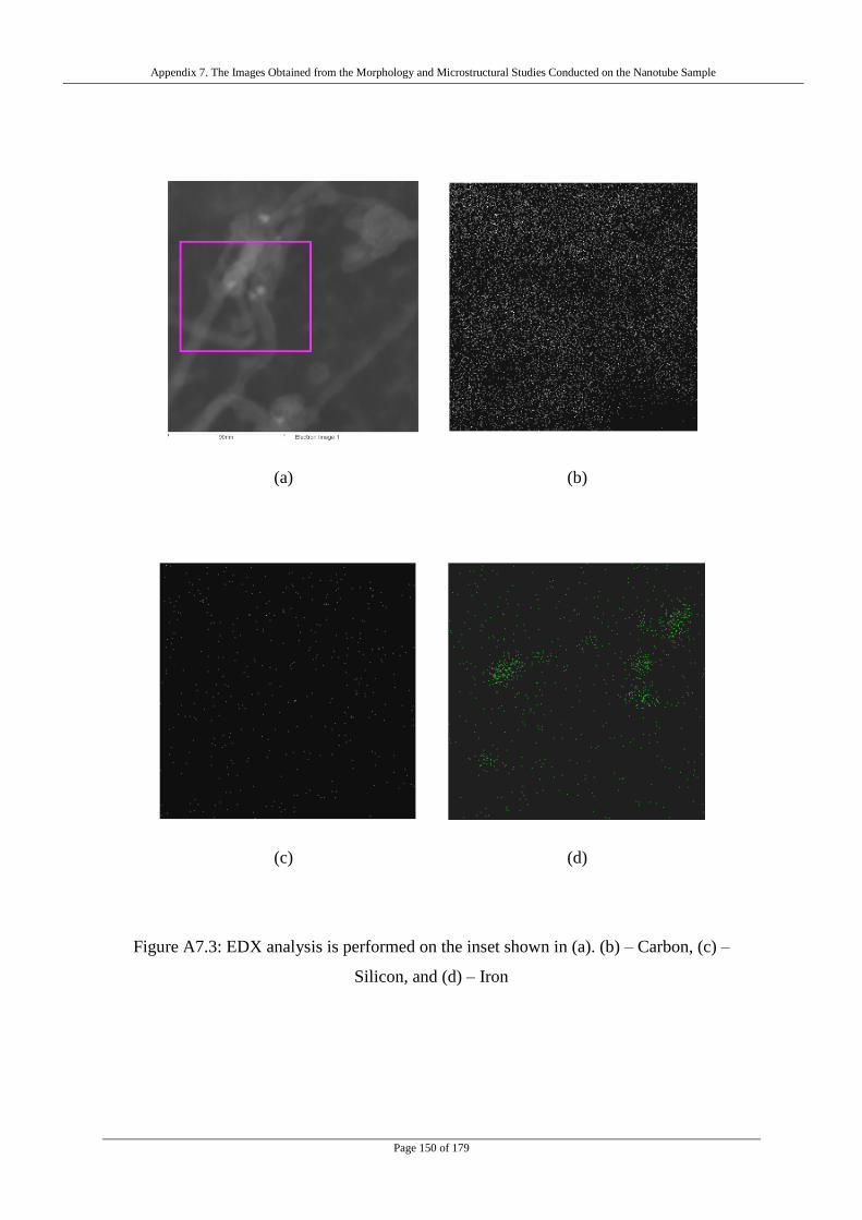
Appendix 7. The Images Obtained from the Morphology and Microstructural Studies Conducted on the Nanotube Sample
Page 150 of 179
(a) (b)
(c) (d)
Figure A7.3: EDX analysis is performed on the inset shown in (a). (b) – Carbon, (c) –
Silicon, and (d) – Iron

Appendix 8. 3D Electromagnetic Simulation of Sapphire Dielectric Resonator for the Microwave Characterisation of Carbon Nanotubes Sample
Page 151 of 179
Appendix 8
A8. 3D Electromagnetic Simulation of Sapphire Dielectric Resonator for
the Microwave Characterisation of Carbon Nanotubes Sample
A8.1 Introduction
Here the electrical conductivity of CNTs is examined by observing the change in the internal
properties of a sapphire resonator when a nanotube powder is inside its cavity. The sapphire
resonator is also modelled using COMSOL multiphysics. Our sapphire resonator model has a
small disc of low-loss high dielectric constant that ensures most of the fields are
contained within the dielectric, which results in a high Q-factor. The dielectric loss is due to a
finite dielectric conductivity, or a finite phase angle between the dielectric polarisation and
the electric field producing it. Therefore, the relative permittivity is complex and written as
(A8.1)
The real part ( of Eq. A8.1 measures the electrical energy stored in the dielectric while the
imaginary part measures the loss in the medium as heat. This heat is due to damping of
the vibrating dipole moments [1]. The radiation loss is very small and the quality factor of the
dielectric is only limited by the losses inside the dielectric body. If the entire field of the
resonant mode is stored inside the resonator and if there are no losses due to external fields,
we have
(A8.2)
The quantity is known as the loss tangent, which is defined as . The
sapphire resonator was used to investigate the surface resistance of the nanotubes. For the
resonant mode, a theoretical analysis of the electromagnetic fields allows the surface
resistance and the current density to be determined from the value of the resonant frequency,

Appendix 8. 3D Electromagnetic Simulation of Sapphire Dielectric Resonator for the Microwave Characterisation of Carbon Nanotubes Sample
Page 152 of 179
-value and dissipated power of the resonator. In dielectric resonators, the dielectric material
in the resonator is used to concentrate the high frequency field on the measurement sample.
The and modes with integer subscripts are used to describe the resonant
modes in dielectric resonators [1,2]. The subscripts and characterise half-period field
variations in the circumferential, radial and axial directions, respectively. Most methods that
measure surface resistance of samples use a resonant mode. The family of
modes is unique because its electric field pattern is purely azimuthal. As shown in Fig. A8.1,
the magnetic field in this mode is solenoidal in nature. Although there is no conducting
material on the side of the walls of the dielectric rod, the mode still has a high -value. The
resonant frequency of the isolated mode in is
(A8.3)
where and represents the radius and length of the dielectric resonator, respectively.
Dielectric rod
Electric Field Line
Magnetic Field Line
Figure A8.1: Field configuration for a resonant mode [3].
For this dielectric resonator method, a sapphire disk is attached permanently to a conducting
plate. The Q-factor of the resonator is mainly dependent on the average value of the surface
resistance of the conducting plate and the measurement sample.

Appendix 8. 3D Electromagnetic Simulation of Sapphire Dielectric Resonator for the Microwave Characterisation of Carbon Nanotubes Sample
Page 153 of 179
A8.2 Sapphire Resonator Model
A cylindrical sapphire resonator-based measurement method is implemented for examining
the electrical properties of CNTs. The main building block of this resonator is the single
crystal sapphire, which has a cavity to allow the insertion of measurement samples. Sapphire
is an anisotropic material and its dielectric constant is dependent on the direction of the
electric field. In the model, the sapphire rod has a diameter of and a length of . To
avoid radiation losses, we enclose the sapphire rod in a cylindrical copper shield. The internal
diameter and the length of the copper shield are 16mm and 10mm, respectively. The model
permits a hole of diameter in the sapphire cavity, and the sample is placed in this gap.
Fig. A8.2 shows a schematic of the sapphire resonator used for this simulation. The resonant
frequency of the resonator is around .
Sapphire Disk
AirCopper radiation shield
(a)
Sapphire Disk
Cavity
(b)
Figure A8.2: A schematic of the cylindrical sapphire resonator. (a) Resonator with the field
lines, dotted lines represent magnetic field patterns while the solid lines represent the electric
field patterns (b) Top view of the structure.

Appendix 8. 3D Electromagnetic Simulation of Sapphire Dielectric Resonator for the Microwave Characterisation of Carbon Nanotubes Sample
Page 154 of 179
The resonant mode of the sapphire dielectric resonator is used for our simulation. The
sapphire resonator was placed in an electromagnetic field, which excites a resonant
mode. Using COMSOL, the conducting sample inside a quartz tube is modelled. It is
good to point out that the quartz tube is assumed to be filled with nanotubes sample.
Therefore, an effective screening from the bulk nanotubes was observed. The loaded quartz
tube is in the cylindrical cavity of the sapphire rod shown in Fig. A8.2. The permittivity of
the sapphire rod is determined from the resonant frequency. The simulation is started by
defining the conductivity of the sample. The sample is in the region of high magnetic field,
which is in the middle of the sapphire rod. Screening current is induced in the sample if its
conductivity is high enough. During the flow of this current, the skin effect arises and
electrons tend to move along the surface of the sample. The estimation of the skin depth is
crucial when predicting how thick the sample in the quartz tube needs to be in order to
minimise field penetration. The computed skin depth is compared to that obtained
theoretically using the known surface resistivity model. The nanotubes in the bulk sample
have various orientations, and there are physical contacts between the nanotubes.
From the quality factor, of the resonator shown in Fig. A8.2, the loss of the resonant
system can be measured. The overall of the resonator device reflects the properties of the
sample occupying the resonator. For this particular sapphire resonator, the is defined as [2]
(A8.4)
(A8.5)
where is the power loss in the sample, is the dielectric power loss and is the
power loss due to fields radiation. The sapphire rod is placed in a closed cavity with high
conductive walls. Therefore, the field radiation is assumed to be zero, leaving us with
and .

Appendix 8. 3D Electromagnetic Simulation of Sapphire Dielectric Resonator for the Microwave Characterisation of Carbon Nanotubes Sample
Page 155 of 179
(A8.6)
where is the sample factor and is the factor of the sapphire rod. For
calculations, we have
(A8.7)
(A8.8)
where is the surface resistance, is the surface area of the cavity, is the volume of the
cavity, is the permeability of free space and is the magnetic field strength. Therefore,
becomes
(A8.9)
For calculations,
(A8.10)
(A8.11)
where is the permittivity of free space, is the permittivity in the air region, is the
permittivity of the dielectric, is the electric field, ins represents the region inside the
dielectric, out represents the air region between the copper shield and the dielectric, is the
total energy stored inside the dielectric and the air around it [2]. Therefore, becomes
(A8.12)

Appendix 8. 3D Electromagnetic Simulation of Sapphire Dielectric Resonator for the Microwave Characterisation of Carbon Nanotubes Sample
Page 156 of 179
A8.3 Simulation Results
The sapphire resonator was designed using the axisymmetric electromagnetics application
mode in COMSOL. The simulation method presents the cylindrical structure of the resonator
as a rectangular geometry due to the nature of this application mode. The modelling plane is a
plane, where the -axis represents the horizontal axis and the -axis represents the
vertical axis. The actual 3D geometry of the model can be obtained by revolving the 2D
geometry around the -axis. Fig. A8.3 shows the 2D and 3D geometries of the sapphire
resonator modelled using COMSOL.
Air
Sapphire
Rod
Copper
Shield
Sample
(a)
Sapphire
Rod
Sample
(b)
Figure A8.3: 2D & 3D geometries of the sapphire resonator modelled using COMSOL.

Appendix 8. 3D Electromagnetic Simulation of Sapphire Dielectric Resonator for the Microwave Characterisation of Carbon Nanotubes Sample
Page 157 of 179
A resonant mode is excited due to the ratio of (0.5) of the
cylindrical resonator. Fig. A8.4 shows the field patterns in the resonator with and without the
sample. Sapphire is a high dielectric material and when operating in the mode, most of
the stored electric energy and magnetic energy are contained within the material. As shown in
Fig. A8.4, the remainder of the energy is distributed around the dielectric resonator in the
space within the shield. Current is driven through the conductive sample using the region
concentrated with magnetic field.
(a)
Sample
(b)
Figure A8.4: The magnetic field pattern in the sapphire resonator simulated using
COMSOL (a) before inserting the conducting sample, (b) after inserting the sample.
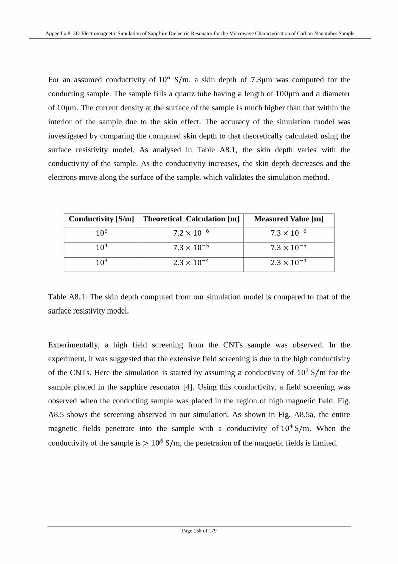
Appendix 8. 3D Electromagnetic Simulation of Sapphire Dielectric Resonator for the Microwave Characterisation of Carbon Nanotubes Sample
Page 158 of 179
For an assumed conductivity of , a skin depth of was computed for the
conducting sample. The sample fills a quartz tube having a length of and a diameter
of . The current density at the surface of the sample is much higher than that within the
interior of the sample due to the skin effect. The accuracy of the simulation model was
investigated by comparing the computed skin depth to that theoretically calculated using the
surface resistivity model. As analysed in Table A8.1, the skin depth varies with the
conductivity of the sample. As the conductivity increases, the skin depth decreases and the
electrons move along the surface of the sample, which validates the simulation method.
Conductivity [S/m] Theoretical Calculation [m] Measured Value [m]
Table A8.1: The skin depth computed from our simulation model is compared to that of the
surface resistivity model.
Experimentally, a high field screening from the CNTs sample was observed. In the
experiment, it was suggested that the extensive field screening is due to the high conductivity
of the CNTs. Here the simulation is started by assuming a conductivity of for the
sample placed in the sapphire resonator [4]. Using this conductivity, a field screening was
observed when the conducting sample was placed in the region of high magnetic field. Fig.
A8.5 shows the screening observed in our simulation. As shown in Fig. A8.5a, the entire
magnetic fields penetrate into the sample with a conductivity of . When the
conductivity of the sample is , the penetration of the magnetic fields is limited.

Appendix 8. 3D Electromagnetic Simulation of Sapphire Dielectric Resonator for the Microwave Characterisation of Carbon Nanotubes Sample
Page 159 of 179
Sapphire Rod
Qu
art
z T
ub
e
Sample
(a)
Qu
art
z T
ub
e
Sample
Sapphire Rod
(b)
Figure A8.5: Field screening observed when the conducting sample is placed in the region of
high magnetic field. (a) Assumed conductivity of , and (b) conductivity of .

Appendix 8. 3D Electromagnetic Simulation of Sapphire Dielectric Resonator for the Microwave Characterisation of Carbon Nanotubes Sample
Page 160 of 179
Also, the conductivity of the sample is varied and the magnetic field strength computed at the
surface of the sample. As shown in Fig. A8.6, the field strength at the surface of the sample
decreases as its conductivity in the simulation is increased. This observation suggests that the
experimental nanotubes sample exhibited screening because it is very conductive.
Figure A8.6: The plot of the magnetic field strength against position along the
surface of the conducting sample with varying conductivity.

Appendix 8. 3D Electromagnetic Simulation of Sapphire Dielectric Resonator for the Microwave Characterisation of Carbon Nanotubes Sample
Page 161 of 179
A8.4 References
[1] D. M. Pozar, Microwave Engineering, Third Edition, John Wiley and Sons, N. Y.,
2005.
[2] D. Kajfez and P. Guillon, Dielectric Resonators, Second Edition, Noble Publishing
Corporation, Atlanta, 1998.
[3] S. J. Fiedziuszko and P. D. Heidmann, Dielectric Resonator Used as a Probe for High
TC Superconductor Measurements, IEEE MTT-S Digest, Pages 555-558, 1989.
[4] J. Baker-Jarvis, M. D. Janezic, and J. H. Lehman, Dielectric Resonator Method for
Measuring the Electrical Conductivity of Carbon Nanotubes from Microwave to
Millimeter Frequencies, Journal of Nanomaterials, Volume 2007, Article ID 24242.

Appendix 9. Publication – Modelling Charge Transport in Graphene Nanoribbons and Carbon Nanotubes using a Schrodinger-Poisson Solver
Page 162 of 179
Appendix 9
A9. Publication - Modelling Charge Transport in Graphene Nanoribbons
and Carbon Nanotubes using a Schrodinger–Poisson Solver

Appendix 10. Publication – Microwave Characterisation of Carbon Nanotube Powders
Page 163 of 179
Appendix 10
A10. Publication - Microwave Characterisation of Carbon Nanotube
Powders