microwave components and circuits€¦ · microwave components and circuits ... lead inductance,...
TRANSCRIPT

2-1
CHAPTER 2
MICROWAVE COMPONENTS AND CIRCUITS
LEARNING OBJECTIVES
Upon completion of this chapter the student will be able to:
1. Explain the basic principles of microwave tubes and describe the limitations of conventional tubes.
2. Describe the basic principles of velocity modulation.
3. Outline the development of microwave tubes.
4. Describe the basic theory of operation of klystrons including multicavity and reflex klystrons.
5. Explain the basic theory of operation of traveling-wave tubes and backward-wave oscillators.
6. Describe the construction, basic theories of operation, and typical applications of magnetrons and amplitrons.
7. Describe the basic theory of operation of tunnel diodes when used in oscillator-, amplifier-, and frequency-converter circuits.
8. Explain the operation of varactors when used in parametric amplifiers and frequency converters.
9. State the basic principles of operation of bulk-effect diodes and the gunn oscillator.
10. Explain the basic operation of passive microwave diodes in terms of theory and application.
11. Explain the basic operation of microwave transistors in terms of theory and application.
MICROWAVE COMPONENTS
The waveguides discussed in chapter 1 serve to transport microwave energy from one place to another. Energy is transported after it has been generated or amplified in a previous stage of the circuit. In this chapter you will be introduced to the special components used in those circuits.
Microwave energy is used in both radar and communications applications. The fact that the frequencies are very high and the wavelengths very short presents special problems in circuit design. Components that were previously satisfactory for signal generation and amplification use are no longer useful in the microwave region. The theory of operation for these components is discussed in this chapter. Because the theory of operation is sometimes difficult to understand, you need to pay particular attention to detail as you study this chapter. It is written in the simplest manner possible while retaining the necessary technical complexity.

2-2
MICROWAVE TUBE PRINCIPLES
The efficiency of conventional tubes is largely independent of frequency up to a certain limit. When frequency increases beyond that limit, several factors combine to rapidly decrease tube efficiency. Tubes that are efficient in the microwave range usually operate on the theory of VELOCITY MODULATION, a concept that avoids the problems encountered in conventional tubes. Velocity modulation is more easily understood if the factors that limit the frequency range of a conventional tube are thoroughly understood. Therefore, the frequency limitations of conventional tubes will be discussed before the concepts and applications of velocity modulation are explained. You may want to review NEETS, Module 6, Introduction to Electronic Emission, Tubes, and Power Supplies, Chapters 1 and 2, for a refresher on vacuum tubes before proceeding.
Frequency Limitations of Conventional Tubes
Three characteristics of ordinary vacuum tubes become increasingly important as frequency rises. These characteristics are interelectrode capacitance, lead inductance, and electron transit time.
The INTERELECTRODE CAPACITANCES in a vacuum tube, at low or medium radio frequencies, produce capacitive reactances that are so large that no serious effects upon tube operation are noticeable. However, as the frequency increases, the reactances become small enough to materially affect the performance of a circuit. For example, in figure 2-1A, a 1-picofarad capacitor has a reactance of 159,000 ohms at 1 megahertz. If this capacitor was the interelectrode capacitance between the grid and plate of a tube, and the rf voltage between these electrodes was 500 volts, then 3.15 milliamperes of current would flow through the interelectrode capacitance. Current flow in this small amount would not seriously affect circuit performance. On the other hand, at a frequency of 100 megahertz the reactance would decrease to approximately 1,590 ohms and, with the same voltage applied, current would increase to 315 milliamperes (figure 2-1B). Current in this amount would definitely affect circuit performance.
Figure 2-1A.—Interelectrode capacitance in a vacuum tube. 1 MEGAHERTZ.

2-3
Figure 2-1B.—Interelectrode capacitance in a vacuum tube. 100 MEGAHERTZ.
Figure 2-1C.—Interelectrode capacitance in a vacuum tube. INTERELECTRODE CAPACITANCE IN A
TUNED-PLATE TUNED-GRID OSCILLATOR.
A good point to remember is that the higher the frequency, or the larger the interelectrode capacitance, the higher will be the current through this capacitance. The circuit in figure 2-1C, shows the interelectrode capacitance between the grid and the cathode (Cgk) in parallel with the signal source. As the frequency of the input signal increases, the effective grid-to-cathode impedance of the tube decreases because of a decrease in the reactance of the interelectrode capacitance. If the signal frequency is 100 megahertz or greater, the reactance of the grid-to-cathode capacitance is so small that much of the signal is short-circuited within the tube. Since the interelectrode capacitances are effectively in parallel with the tuned circuits, as shown in figures 2-1A, B, and C, they will also affect the frequency at which the tuned circuits resonate.
Another frequency-limiting factor is the LEAD INDUCTANCE of the tube elements. Since the lead inductances within a tube are effectively in parallel with the interelectrode capacitance, the net effect is to raise the frequency limit. However, the inductance of the cathode lead is common to both the grid and plate circuits. This provides a path for degenerative feedback which reduces overall circuit efficiency.
2-4
A third limitation caused by tube construction is TRANSIT TIME. Transit time is the time required for electrons to travel from the cathode to the plate. While some small amount of transit time is required for electrons to travel from the cathode to the plate, the time is insignificant at low frequencies. In fact, the transit time is so insignificant at low frequencies that it is generally not considered to be a hindering factor. However, at high frequencies, transit time becomes an appreciable portion of a signal cycle and begins to hinder efficiency. For example, a transit time of 1 nanosecond, which is not unusual, is only 0.001 cycle at a frequency of 1 megahertz. The same transit time becomes equal to the time required for an entire cycle at 1,000 megahertz. Transit time depends on electrode spacing and existing voltage potentials. Transit times in excess of 0.1 cycle cause a significant decrease in tube efficiency. This decrease in efficiency is caused, in part, by a phase shift between plate current and grid voltage.
If the tube is to operate efficiently, the plate current must be in phase with the grid-signal voltage and 180 degrees out of phase with the plate voltage. When transit time approaches 1/4 cycle, this phase relationship between the elements does not hold true. A positive swing of a high-frequency grid signal causes electrons to leave the cathode and flow to the plate. Initially this current is in phase with the grid voltage. However, since transit time is an appreciable part of a cycle, the current arriving at the plate now lags the grid-signal voltage. As a result, the power output of the tube decreases and the plate power dissipation increases. Another loss of power occurs because of ELECTROSTATIC INDUCTION.
The electrons forming the plate current also electrostatically induce potentials in the grid as they move past it. This electrostatic induction in the grid causes currents of positive charges to move back and forth in the grid structure. This back and forth action is similar to the action of hole current in semiconductor devices. When transit-time effect is not a factor (as in low frequencies), the current induced in one side of the grid by the approaching electrons is equal to the current induced on the other side by the receding electrons. The net effect is zero since the currents are in opposite directions and cancel each other. However, when transit time is an appreciable part of a cycle, the number of electrons approaching the grid is not always equal to the number going away. As a result, the induced currents do not cancel. This uncancelled current produces a power loss in the grid that is considered resistive in nature. In other words, the tube acts as if a resistor were connected between the grid and the cathode. The resistance of this imaginary resistor decreases rapidly as the frequency increases. The resistance may become so low that the grid is essentially short-circuited to the cathode, preventing proper operation of the tube.
Several methods are available to reduce the limitations of conventional tubes, but none work well when frequency increases beyond 1,000 megahertz. Interelectrode capacitance can be reduced by moving the electrodes further apart or by reducing the size of the tube and its electrodes. Moving the electrodes apart increases the problems associated with transit time, and reducing the size of the tube lowers the power-handling capability. You can see that efforts to reduce certain limitations in conventional tubes are compromises that are often in direct opposition to each other. The net effect is an upper limit of approximately 1,000 megahertz, beyond which conventional tubes are not practical.
Q-1. What happens to the impedance of interelectrode capacitance as frequency increases?
Q-2. What undesirable effect is caused by the inductance of the cathode lead?
Q-3. How does transit time affect the relationship of the grid voltage and the plate current at high frequencies?
Q-4. Moving tube electrodes apart to decrease interelectrode capacitance causes an increase in the effect of what property?

2-5
Velocity Modulation
The microwave tube was developed when the use of the frequency spectrum went beyond 1,000 megahertz and into the microwave range. The microwave tube uses transit time in the conversion of dc power to radio-frequency (rf) power. The interchange of power is accomplished by using the principle of electron VELOCITY MODULATION and low-loss resonant cavities in the microwave tube.
A clear understanding of microwave tubes must start with an understanding of how electrons and electric fields interact. An electron has mass and thus exhibits kinetic energy when in motion. The amount of kinetic energy in an electron is directly proportional to its velocity; that is, the higher the velocity, the higher the energy level. The basic concept of the electron energy level being directly related to electron velocity is the key principle of energy transfer and amplification in microwave tubes.
An electron can be accelerated or decelerated by an electrostatic field. Figure 2-2 shows an electron moving in an electrostatic field. The direction of travel (shown by the heavy arrow) is against the electrostatic lines of force which are from positive to negative. The negatively charged electron will be attracted to the positively charged body and will increase in velocity. As its velocity increases, the energy level of the electron will also increase. Where does the electron acquire its additional energy? The only logical source is from the electrostatic field. Thus, the conclusion is clear. An electron traveling in a direction opposite to electrostatic lines of force will absorb energy and increase in velocity (accelerate).
Figure 2-2.—Moving electron gaining velocity and energy.
As figure 2-3 illustrates, the opposite condition is also true. An electron traveling in the same direction as the electrostatic lines of force will decelerate by giving up energy to the field. The negatively charged body will repel the electron and cause it to decrease in velocity. When the velocity is reduced, the energy level is also reduced. The energy lost by the electron is gained by the electrostatic field.
+ + + + + +
- - - - - -NTS110202
ELECTRON
POSITIVELY CHARGEDBODY
ELECTRIC FIELD
NEGATIVELY CHARGEDBODY

2-6
Figure 2-3.—Moving electron losing energy and velocity.
The operation of a velocity-modulated tube depends on a change in the velocity of the electrons passing through its electrostatic field. A change in electron velocity causes the tube to produce BUNCHES of electrons. These bunches are separated by spaces in which there are relatively few electrons. Velocity modulation is then defined as that variation in the velocity of a beam of electrons caused by the alternate speeding up and slowing down of the electrons in the beam. This variation is usually caused by a voltage signal applied between the grids through which the beam must pass.
The first requirement in obtaining velocity modulation is to produce a stream of electrons which are all traveling at the same speed. The electron stream is produced by an electron gun. A simplified version of an electron gun is shown in figure 2-4A. Electrons emitted from the cathode are attracted toward the positive accelerator grid and all but a few of the electrons pass through the grid and form a beam. The electron beam then passes through a pair of closely spaced grids, called BUNCHER GRIDS. Each grid is connected to one side of a tuned circuit. The parallel-resonant tuned circuit (figure 2-4A) in the illustration represents the doughnut-shaped resonant cavity surrounding the electron stream (figure 2-4B). The buncher grids are the dashed lines at the center of the cavity and are at the same dc potential as the accelerator grid. The alternating voltage which exists across the resonant circuit causes the velocity of the electrons leaving the buncher grids to differ from the velocity of the electrons arriving at the buncher grids. The amount of difference depends on the strength and direction of the electrostatic field within the resonant cavity as the electrons pass through the grids.
Figure 2-4A.—Electron gun with buncher grids.

2-7
Figure 2-4B.—Electron gun with buncher grids.
The manner in which the buncher produces bunches of electrons is better understood by considering the motions of individual electrons, as illustrated in figure 2-5A.
When the voltage across the grids is negative, as shown in figure 2-5B, electron 1 crossing the gap at that time is slowed. Figure 2-5C shows the potential across the gap at 0 volts; electron 2 is not affected. Electron 3 enters the gap (figure 2-5D) when the voltage across the gap is positive and its velocity is increased. The combined effect is shown in figure 2-5E. All of the electrons in the group have been bunched closer together.
Figure 2-5A.—Buncher cavity action. BUNCHER CAVITY.
Figure 2-5B.—Buncher cavity action. ELECTRON #1 DECELERATED.

2-8
Figure 2-5C.—Buncher cavity action. ELECTRON #2 VELOCITY UNCHANGED.
Figure 2-5D.—Buncher cavity action. ELECTRON #3 ACCELERATED.
Figure 2-5E.—Buncher cavity action. ELECTRONS BEGINNING TO BUNCH, DUE TO VELOCITY
DIFFERENCES.
The velocity modulation of the beam is merely a means to an end. No useful power has been produced at this point. The energy gained by the accelerated electrons is balanced by the energy lost by the decelerated electrons. However, a new and useful beam distribution will be formed if the velocity-modulated electrons are allowed to drift into an area that has no electrostatic field.
As the electrons drift into the field-free area beyond the buncher cavity, bunches continue to form because of the new velocity relationships between the electrons. Unless the beam is acted upon by some other force, these bunches will tend to form and disperse until the original beam distribution is eventually reformed. The net effect of velocity modulation is to form a current-density modulated beam that varies at the same rate as the grid-signal frequency. The next step is to take useful power from the beam.
The current-modulated (bunched) electron beam in figure 2-6A and B is shown in various stages of formation and dispersion. A second cavity, called a CATCHER CAVITY, must be placed at a point of

2-9
maximum bunching to take useful energy from the beam (shown in figure 2-6B). The physical position of the catcher cavity is determined by the frequency of the buncher-grid signal because this signal determines the transit time of the electron bunches. Note also that both cavities are resonant at the buncher-grid frequency. The electron bunches will induce an rf voltage in the grid gap of the second cavity causing it to oscillate. Proper placement of the second cavity will cause the induced grid-gap voltage to decelerate the electron bunches as they arrive at the gap. Since the largest concentration of electrons is in the bunches, slowing the bunches causes a transfer of energy to the output cavity. The balance of energy has been disturbed because the placement of the catcher cavity is such that bunches are slowed down when they arrive at the cavity. The areas between bunches arrive at the cavity at just the right time. At this time the voltage is of the correct polarity to increase the velocity of the electrons and the beam absorbs energy. The areas between the bunches have very few electrons, so the energy removed from the beam is much greater than the energy required to speed up the electrons between the bunches. Therefore, if the second cavity is properly positioned, useful energy can be removed from a velocity-modulated electron beam.
Q-5. The kinetic energy of an electron is directly proportional to what property?
Q-6. What will be the effect upon an electron traveling in the opposite direction to the lines of force in an electrostatic field?
Q-7. How is a beam of electrons velocity-modulated?
Q-8. What portion of an electron gun causes the electrons to accelerate or decelerate?
RESONANT CAVITY(BUNCHER)
NTS110206
GRIDSDIRECTION OF ELECTRON BEAM
BUNCHING OCCURS (VELOCITY MODULATION)
BUNCHERCAVITY
CATCHER CAVITY AT POINTOF MAXIMUM BUNCHING
BUNCHES OF ELECTRONS
ENERGY REMOVED BY CATCHER CAVITY
A
B
Figure 2-6A-B.—Removing energy from a velocity-modulated beam.

2-10
Q-9. What is the effect upon an electron that enters the buncher gap when the potential across the grids is at 0 volts?
Q-10. What determines the placement of the catcher cavity?
MICROWAVE TUBES
Microwave tubes perform the same functions of generation and amplification in the microwave portion of the frequency spectrum that vacuum tubes perform at lower frequencies. This section will explain the basic operation of the most widely used microwave tubes, including klystrons, traveling-wave tubes, backward-wave oscillators, magnetrons, and crossed-field amplifiers. The variations of these tubes for use in specific applications are so numerous that all of them cannot be discussed in this module. However, general principles of operation are similar in all of the variations so the explanations will be restricted to the general principles of operation.
The Basic Two-Cavity Klystron
Klystrons are velocity-modulated tubes that are used in radar and communications equipment as oscillators and amplifiers. Klystrons make use of the transit-time effect by varying the velocity of an electron beam in much the same manner as the previously discussed velocity-modulation process. Strong electrostatic fields are necessary in the klystron for efficient operation. This is necessary because the interaction of the signal and the electron beam takes place in a very short distance.
The construction and essential components of a TWO-CAVITY KLYSTRON are shown in figure 2-7A. Figure 2-7B is a schematic representation of the same tube. When the tube is energized, the cathode emits electrons which are focused into a beam by a low positive voltage on the control grid. The beam is then accelerated by a very high positive dc potential that is applied in equal amplitude to both the accelerator grid and the buncher grids. The buncher grids are connected to a cavity resonator that superimposes an ac potential on the dc voltage. Ac potentials are produced by oscillations within the cavity that begin spontaneously when the tube is energized. The initial oscillations are caused by random fields and circuit imbalances that are present when the circuit is energized. The oscillations within the cavity produce an oscillating electrostatic field between the buncher grids that is at the same frequency as the natural frequency of the cavity. The direction of the field changes with the frequency of the cavity. These changes alternately accelerate and decelerate the electrons of the beam passing through the grids. The area beyond the buncher grids is called the DRIFT SPACE. The electrons form bunches in this area when the accelerated electrons overtake the decelerated electrons.

2-11
Figure 2-7A.—Functional and schematic diagram of a two-cavity klystron.
Figure 2-7B.—Functional and schematic diagram of a two-cavity klystron.
The function of the CATCHER GRIDS is to absorb energy from the electron beam. The catcher grids are placed along the beam at a point where the bunches are fully formed. The location is determined by the transit time of the bunches at the natural resonant frequency of the cavities (the resonant frequency of the catcher cavity is the same as the buncher cavity). The location is chosen because maximum energy transfer to the output (catcher) cavity occurs when the electrostatic field is of the correct polarity to slow down the electron bunches.
The two-cavity klystron in figure 2-7A and B may be used either as an oscillator or an amplifier. The configuration shown in the figure is correct for oscillator operation. The feedback path provides energy of the proper delay and phase relationship to sustain oscillations. A signal applied at the buncher grids will be amplified if the feedback path is removed.
Q-11. What is the basic principle of operation of a klystron?

2-12
Q-12. The electrons in the beam of a klystron are speeded up by a high dc potential applied to what elements?
Q-13. The two-cavity klystron uses what cavity as an output cavity?
Q-14. A two-cavity klystron without a feedback path will operate as what type of circuit?
The Multicavity Power Klystron
Klystron amplification, power output, and efficiency can be greatly improved by the addition of intermediate cavities between the input and output cavities of the basic klystron. Additional cavities serve to velocity-modulate the electron beam and produce an increase in the energy available at the output. Since all intermediate cavities in a multicavity klystron operate in the same manner, a representative THREE-CAVITY KLYSTRON will be discussed.
A three-cavity klystron is illustrated in figure 2-8. The entire DRIFT-TUBE ASSEMBLY, the three CAVITIES, and the COLLECTOR PLATE of the three-cavity klystron are operated at ground potential for reasons of safety. The electron beam is formed and accelerated toward the drift tube by a large negative pulse applied to the cathode. MAGNETIC FOCUS COILS are placed around the drift tube to keep the electrons in a tight beam and away from the side walls of the tube. The focus of the beam is also aided by the concave shape of the cathode in high-powered klystrons.
Figure 2-8.—Three-cavity klystron.
NTS110208
INPUTPULSE
INPUTCAVITY
DR
IFT
-TU
BE
AS
SE
MB
LY
OUTPUTCAVITY
AMPLIFIEDOUTPUTPULSE
EL
EC
TR
ON
GU
N
PL
AT
EA
SS
EM
BLY
(CO
LL
EC
TO
R)
µ1 s
µ1 s

2-13
The output of any klystron (regardless of the number of cavities used) is developed by velocity modulation of the electron beam. The electrons that are accelerated by the cathode pulse are acted upon by rf fields developed across the input and middle cavities. Some electrons are accelerated, some are decelerated, and some are unaffected. Electron reaction depends on the amplitude and polarity of the fields across the cavities when the electrons pass the cavity gaps. During the time the electrons are traveling through the drift space between the cavities, the accelerated electrons overtake the decelerated electrons to form bunches. As a result, bunches of electrons arrive at the output cavity at the proper instant during each cycle of the rf field and deliver energy to the output cavity.
Only a small degree of bunching takes place within the electron beam during the interval of travel from the input cavity to the middle cavity. The amount of bunching is sufficient, however, to cause oscillations within the middle cavity and to maintain a large oscillating voltage across the input gap. Most of the velocity modulation produced in the three-cavity klystron is caused by the voltage across the input gap of the middle cavity. The high voltage across the gap causes the bunching process to proceed rapidly in the drift space between the middle cavity and the output cavity. The electron bunches cross the gap of the output cavity when the gap voltage is at maximum negative. Maximum energy transfer from the electron beam to the output cavity occurs under these conditions. The energy given up by the electrons is the kinetic energy that was originally absorbed from the cathode pulse.
Klystron amplifiers have been built with as many as five intermediate cavities in addition to the input and output cavities. The effect of the intermediate cavities is to improve the electron bunching process which improves amplifier gain. The overall efficiency of the tube is also improved to a lesser extent. Adding more cavities is roughly the same as adding more stages to a conventional amplifier. The overall amplifier gain is increased and the overall bandwidth is reduced if all the stages are tuned to the same frequency. The same effect occurs with multicavity klystron tuning. A klystron amplifier tube will deliver high gain and a narrow bandwidth if all the cavities are tuned to the same frequency. This method of tuning is called SYNCHRONOUS TUNING. If the cavities are tuned to slightly different frequencies, the gain of the amplifier will be reduced but the bandwidth will be appreciably increased. This method of tuning is called STAGGERED TUNING.
Q-15. What can be added to the basic two-cavity klystron to increase the amount of velocity modulation and the power output?
Q-16. How is the electron beam of a three-cavity klystron accelerated toward the drift tube?
Q-17. Which cavity of a three-cavity klystron causes most of the velocity modulation?
Q-18. In a multicavity klystron, tuning all the cavities to the same frequency has what effect on the bandwidth of the tube?
Q-19. The cavities of a multicavity klystron are tuned to slightly different frequencies in what method of tuning?
The Reflex Klystron
Another tube based on velocity modulation, and used to generate microwave energy, is the REFLEX KLYSTRON (figure 2-9). The reflex klystron contains a REFLECTOR PLATE, referred to as the REPELLER, instead of the output cavity used in other types of klystrons. The electron beam is modulated as it was in the other types of klystrons by passing it through an oscillating resonant cavity, but here the similarity ends. The feedback required to maintain oscillations within the cavity is obtained by reversing the beam and sending it back through the cavity. The electrons in the beam are velocity-modulated before the beam passes through the cavity the second time and will give up the energy required to maintain

2-14
oscillations. The electron beam is turned around by a negatively charged electrode that repels the beam. This negative element is the repeller mentioned earlier. This type of klystron oscillator is called a reflex klystron because of the reflex action of the electron beam.
Figure 2-9.—Functional diagram of a reflex klystron.
Three power sources are required for reflex klystron operation: (1) filament power, (2) positive resonator voltage (often referred to as beam voltage) used to accelerate the electrons through the grid gap of the resonant cavity, and (3) negative repeller voltage used to turn the electron beam around. The electrons are focused into a beam by the electrostatic fields set up by the resonator potential (B+) in the body of the tube. Note in figure 2-9 that the resonator potential is common to the resonator cavity, the accelerating grid, and the entire body of the tube.
The resonator potential also causes the resonant cavity to begin oscillating at its natural frequency when the tube is energized. These oscillations cause an electrostatic field across the grid gap of the cavity that changes direction at the frequency of the cavity. The changing electrostatic field affects the electrons in the beam as they pass through the grid gap. Some are accelerated and some are decelerated, depending upon the polarity of the electrostatic field as they pass through the gap. Figure 2-10, view (A), illustrates the three possible ways an electron can be affected as it passes through the gap (velocity increasing, decreasing, or remaining constant). Since the resonant cavity is oscillating, the grid potential is an alternating voltage that causes the electrostatic field between the grids to follow a sine-wave curve as shown in figure 2-10, view (B). As a result, the velocity of the electrons passing through the gap is affected uniformly as a function of that sine wave. The amount of velocity change is dependent on the strength and polarity of the grid voltage.

2-15
Figure 2-10.—Electron bunching diagram.
The variation in grid voltage causes the electrons to enter the space between the grid and the repeller at various velocities. For example, in figure 2-10, views (A) and (B), the electrons at times 1 and 2 are speeded up as they pass through the grid. At time 3, the field is passing through zero and the electron is unaffected. At times 4 and 5, the grid field is reversed; the electrons give up energy because their velocity is reduced as they pass through the grids.
The distance the electrons travel in the space separating the grid and the repeller depends upon their velocity. Those moving at slower velocities, such as the electron at time 4, move only a short distance from the grid before being affected by the repeller voltage. When this happens, the electron is forced by the repeller voltage to stop, reverse direction, and return toward the grid. The electrons moving at higher velocities travel further beyond the grid before reversing direction because they have greater momentum. If the repeller voltage is set at the correct value, the electrons will form a bunch around the constant-speed electrons. The electrons will then return to the grid gap at the instant the electrostatic field is at the correct polarity to cause maximum deceleration of the bunch. This action is also illustrated in figure 2-10, view (A). When the grid field provides maximum deceleration, the returning electrons release maximum energy to the grid field which is in phase with cavity current. Thus, the returning electrons supply the regenerative feedback required to maintain cavity oscillations.
The constant-speed electrons must remain in the reflecting field space for a minimum time of 3/4 cycle of the grid field for maximum energy transfer. The period of time the electrons remain in the repeller field is determined by the amount of negative repeller voltage. The reflex klystron will continue to oscillate if the electrons remain in the repeller field longer than 3/4 cycle (as long as the electrons return to the grid gap when the field is of the proper polarity to decelerate the electrons). Figure 2-11 shows the effect of the repeller field on the electron bunch for 3/4 cycle and for 1 3/4 cycles. Although not shown in the figure, the constant-velocity electrons may remain in the repeller field for any number of cycles over the minimum 3/4 cycle. If the electrons remain in the field for longer than 3/4 cycle, the difference in electron transit time causes the tube performance characteristics to change. The differences in operating characteristics are identified by MODES OF OPERATION.

2-16
Figure 2-11.—Bunching action of a reflex klystron.
The reflex klystron operates in a different mode for each additional cycle that the electrons remain in the repeller field. Mode 1 is obtained when the repeller voltage produces an electron transit time of 3/4 cycle. Additional modes follow in sequence. Mode 2 has an electron transit time of 1 3/4 cycles; mode 3 has an electron transit time of 2 3/4 cycles; etc. The physical design of the tube limits the number of modes possible in practical applications. A range of four modes of operation are normally available. The actual mode used (1 3/4 cycles through 4 3/4 cycles, 2 3/4 cycles through 6 3/4 cycles, etc.) depends upon the application. The choice of mode is determined by the difference in power available from each mode and the band of frequencies over which the circuit can be tuned.
OUTPUT POWER.—The variation in output power for different modes of operation can be explained by examining the factors which limit the amplitude of oscillations. Power and amplitude limitations are caused by the DEBUNCHING process of the electrons in the repeller field space. Debunching is simply the spreading out of the electron bunches before they reach electrostatic fields across the cavity grid . The lower concentration of electrons in the returning bunches provides less power for delivery to the oscillating cavity. This reduced power from the bunches, in turn, reduces the amplitude of the cavity oscillations and causes a decrease in output power. In higher modes of operation the electron bunches are formed more slowly. They are more likely to be affected by debunching because of mutual repulsion between the negatively charged electrons. The long drift time in the higher modes allows more time for this electron interaction and, as a result, the effects of debunching are more severe. The mutual repulsion changes the relative velocity between the electrons in the bunches and causes the bunches to spread out.

2-17
Figure 2-12 illustrates the ELECTRONIC TUNING (tuning by altering the repeller voltage) range and output power of a reflex klystron. Each mode has a center frequency of 3,000 megahertz which is predetermined by the physical size of the cavity. The output power increases as the repeller voltage is made more negative. This is because the transit time of the electron bunches is decreased.
Figure 2-12.—Electronic tuning and output power of a reflex klystron.
Electronic tuning does not change the center frequency of the cavity, but does vary the frequency within the mode of operation. The amount the frequency can be varied above or below the center frequency is limited by the half-power points of the mode, as shown in figure 2-12. The center frequency can be changed by one of two methods One method, GRID-GAP TUNING, varies the cavity frequency by altering the distance between the grids to change the physical size of the cavity. This method varies the capacitance of the cavity by using a tuning screw to change the distance between the grids mechanically. The cavity can also be tuned by PADDLES or SLUGS that change the inductance of the cavity.
Q-20. What element of the reflex klystron replaces the output cavity of a normal klystron?
Q-21. When the repealer potential is constant, what property of the electron determines how long it will remain in the drift space of the reflex klystron?
Q-22. The constant-speed electrons of an electron bunch in a reflex klystron must remain in the repeller field for what minimum time?
Q-23. If the constant-speed electrons in a reflex klystron remain in the repeller field for 1 3/4 cycles, what is the mode of operation?

2-18
Q-24. Debunching of the electron bunches in the higher modes of a reflex klystron has what effect on output power?
Q-25. What limits the tuning range around the center frequency of a reflex klystron in a particular mode of operation?
The Decibel Measurement System
Because of the use of the decibel measurement system in the following paragraphs, you will be introduced to it at this point. Technicians who deal with communications and radar equipment most often speak of the gain of an amplifier or a system in terms of units called DECIBELS (dB). Throughout your Navy career you will use decibels as an indicator of equipment performance; therefore, you need to have a basic understanding of the decibel system of measurement. Because the actual calculation of decibel measurements is seldom required in practical applications, the explanation given in this module is somewhat simplified. Most modern test equipment is designed to measure and indicate decibels directly which eliminates the need for complicated mathematical calculations. Nevertheless, a basic explanation of the decibel measurement system is necessary for you to understand the significance of dB readings and equipment gain ratings which are expressed in decibels.
The basic unit of measurement in the system is not the decibel, but the bel, named in honor of the American inventor, Alexander Graham Bell. The bel is a unit that expresses the logarithmic ratio between the input and output of any given component, circuit, or system and may be expressed in terms of voltage, current, or power. Most often it is used to show the ratio between input and output power. The formula is as follows:
The gain of an amplifier can be expressed in bels by dividing the output (P1) by the input (P2) and taking the base 10 logarithm of the resulting quotient. Thus, if an amplifier doubles the power, the quotient will be 2. If you consult a logarithm table, you will find that the base 10 logarithm of 2 is 0.3; so the power gain of the amplifier is 0.3 bel. Experience has taught that because the bel is a rather large unit, it is difficult to apply. A more practical unit that can be applied more easily is the decibel (1/10 bel). Any figure expressed in bels can easily be converted to decibels by multiplying the figure by 10 or simply by moving the decimal one place to the right. The previously found ratio of 0.3 is therefore equal to 3 decibels.
The reason for using the decibel system when expressing signal strength may be seen in the power ratios in table 2-1. For example, to say that a reference signal has increased 50 dB is much easier than to say the output has increased 100,000 times. The amount of increase or decrease from a chosen reference level is the basis of the decibel measurement system, not the reference level itself. Whether the input power is increased from 1 watt to 100 watts or from 1,000 watts to 100,000 watts, the amount of increase is still 20 decibels.

2-19
Table 2-1.—Decibel Power Ratios
Source Level (dB) Power Ratio 1 = 1.3 3 = 2.0 5 = 3.2 6 = 4.0 7 = 5.0
10 = 10 = 101 20 = 100 = 102 30 = 1000 = 103 40 = 10,000 = 104 50 = 100,000 = 105 60 = 1,000,000 = 106 70 = 10,000,000 = 107
100 = 1010 110 = 1011 140 = 1014
Examine table 2-1 again, and take particular note of the power ratios for source levels of 3 dB and 6 dB. As the table illustrates, an increase of 3 dB represents a doubling of power. The reverse is also true. If a signal decreases by 3 dB, half the power is lost. For example, a 1,000 watt signal decreased by 3 dB will equal 500 watts while a 1,000 watt signal increased by 3 dB equals 2,000 watts.
The attenuator is a widely used piece of test equipment that can be used to demonstrate the importance of the decibel as a unit of measurement. Attenuators are used to reduce a signal to a smaller level for use or measurement. Most attenuators are rated by the number of decibels the signal is reduced. The technician's job is to know the relationship between the dB rating and the power reduction it represents. This is so important, in fact, that every student of electronics should memorize the relationships in table 2-1 through the 60 dB range. The technician will have to apply this knowledge to prevent damage to valuable equipment. A helpful hint is to note that the first digit of the source level (on the chart) is the same number as the corresponding power of 10 exponent; i.e., 40 dB = 1 × 10⁴ or 10,000. A 20 dB attenuator, for example, will reduce an input signal by a factor of 100. In other words, a 100-milliwatt signal will be reduced to 1 milliwatt. A 30 dB attenuator will reduce the same 100-milliwatt signal by a factor of 1,000 and produce an output of 0.1 milliwatt. When an attenuator of the required size is not available, attenuators of several smaller sizes may be added directly together to reach the desired amount of attenuation. A 10 dB attenuator and a 20 dB attenuator add directly to equal 30 dB of attenuation. The same relationship exists with amplifier stages as well. If an amplifier has two stages rated at 10 dB each, the total amplifier gain will be 20 dB.
When you speak of the dB level of a signal, you are really speaking of a logarithmic comparison between the input and output signals. The input signal is normally used as the reference level. However, the application sometimes requires the use of a standard reference signal. The most widely used reference level is a 1-milliwatt signal. The standard decibel abbreviation of dB is changed to dBm to indicate the use of the 1-milliwatt standard reference. Thus, a signal level of +3 dBm is 3 dB above 1 milliwatt, and a signal level of −3 dBm is 3 dB below 1 milliwatt. Whether using dB or dBm, a plus (+) sign (or no sign at all) indicates the output signal is larger than the reference; a minus (−) sign indicates the output signal is less than the reference.
2-20
The Navy student of electronics will encounter the dBm system of measurement most often as a figure indicating the receiver sensitivity of radar or communications equipment. Typically, a radar receiver will be rated at approximately −107 dBm, which means the receiver will detect a signal 107 dB below 1 milliwatt.
The importance of understanding the decibel system of measurement can easily be seen in the case of receiver-sensitivity measurements. At first glance a loss of 3 dBm from a number as large as −107 dBm seems insignificant; however, it becomes extremely important when the number indicates receiver sensitivity in the decibel system. When the sensitivity falls to −104 dBm, the receiver will only detect a signal that is twice as large as a signal at −107 dBm.
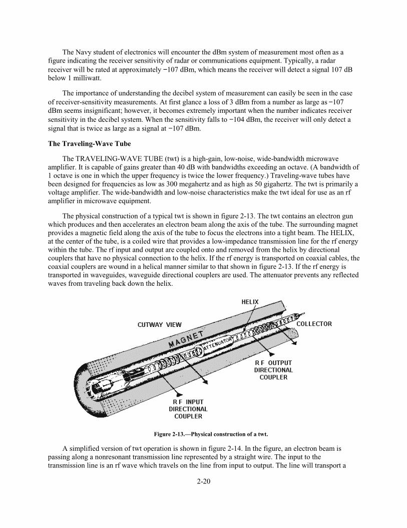
The Traveling-Wave Tube
The TRAVELING-WAVE TUBE (twt) is a high-gain, low-noise, wide-bandwidth microwave amplifier. It is capable of gains greater than 40 dB with bandwidths exceeding an octave. (A bandwidth of 1 octave is one in which the upper frequency is twice the lower frequency.) Traveling-wave tubes have been designed for frequencies as low as 300 megahertz and as high as 50 gigahertz. The twt is primarily a voltage amplifier. The wide-bandwidth and low-noise characteristics make the twt ideal for use as an rf amplifier in microwave equipment.
The physical construction of a typical twt is shown in figure 2-13. The twt contains an electron gun which produces and then accelerates an electron beam along the axis of the tube. The surrounding magnet provides a magnetic field along the axis of the tube to focus the electrons into a tight beam. The HELIX, at the center of the tube, is a coiled wire that provides a low-impedance transmission line for the rf energy within the tube. The rf input and output are coupled onto and removed from the helix by directional couplers that have no physical connection to the helix. If the rf energy is transported on coaxial cables, the coaxial couplers are wound in a helical manner similar to that shown in figure 2-13. If the rf energy is transported in waveguides, waveguide directional couplers are used. The attenuator prevents any reflected waves from traveling back down the helix.
Figure 2-13.—Physical construction of a twt.
A simplified version of twt operation is shown in figure 2-14. In the figure, an electron beam is passing along a nonresonant transmission line represented by a straight wire. The input to the transmission line is an rf wave which travels on the line from input to output. The line will transport a
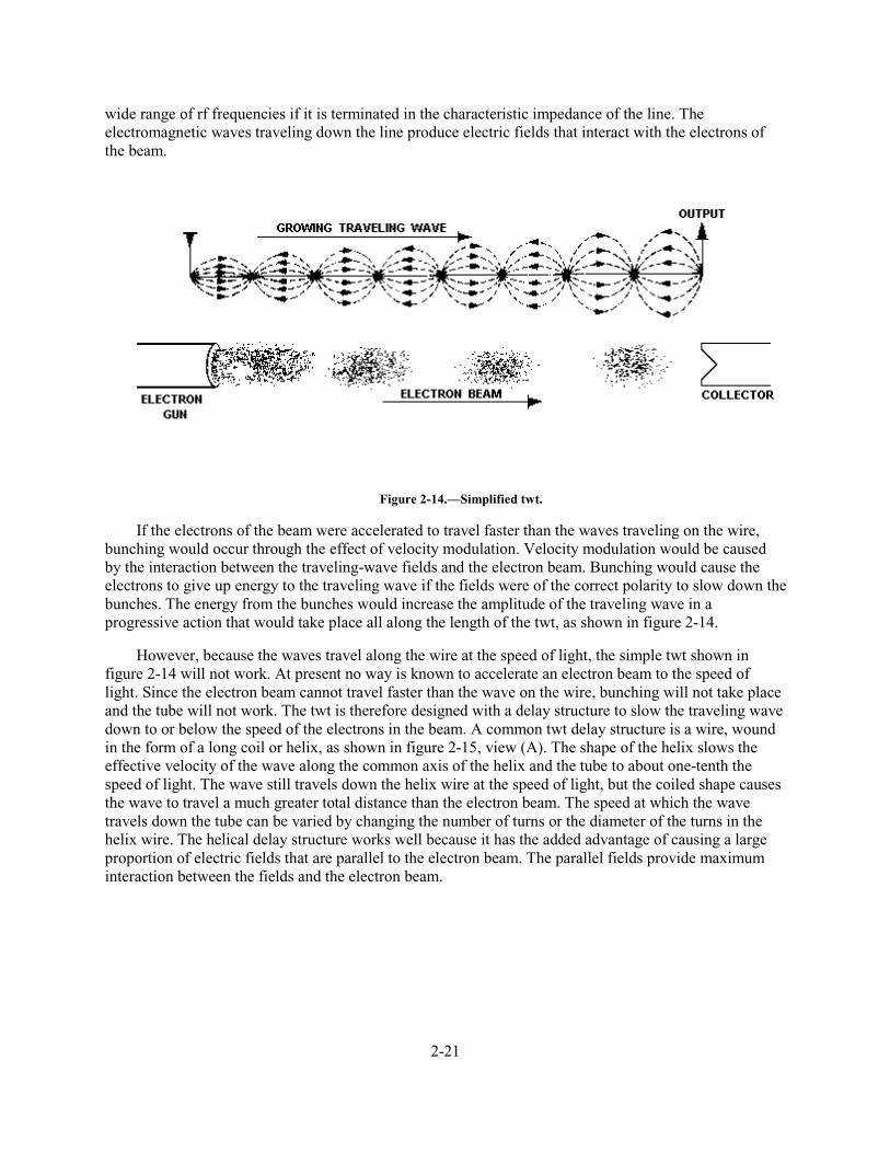
2-21
wide range of rf frequencies if it is terminated in the characteristic impedance of the line. The electromagnetic waves traveling down the line produce electric fields that interact with the electrons of the beam.
Figure 2-14.—Simplified twt.
If the electrons of the beam were accelerated to travel faster than the waves traveling on the wire, bunching would occur through the effect of velocity modulation. Velocity modulation would be caused by the interaction between the traveling-wave fields and the electron beam. Bunching would cause the electrons to give up energy to the traveling wave if the fields were of the correct polarity to slow down the bunches. The energy from the bunches would increase the amplitude of the traveling wave in a progressive action that would take place all along the length of the twt, as shown in figure 2-14.
However, because the waves travel along the wire at the speed of light, the simple twt shown in figure 2-14 will not work. At present no way is known to accelerate an electron beam to the speed of light. Since the electron beam cannot travel faster than the wave on the wire, bunching will not take place and the tube will not work. The twt is therefore designed with a delay structure to slow the traveling wave down to or below the speed of the electrons in the beam. A common twt delay structure is a wire, wound in the form of a long coil or helix, as shown in figure 2-15, view (A). The shape of the helix slows the effective velocity of the wave along the common axis of the helix and the tube to about one-tenth the speed of light. The wave still travels down the helix wire at the speed of light, but the coiled shape causes the wave to travel a much greater total distance than the electron beam. The speed at which the wave travels down the tube can be varied by changing the number of turns or the diameter of the turns in the helix wire. The helical delay structure works well because it has the added advantage of causing a large proportion of electric fields that are parallel to the electron beam. The parallel fields provide maximum interaction between the fields and the electron beam.
2-22
Figure 2-15.—Functional diagram of a twt.
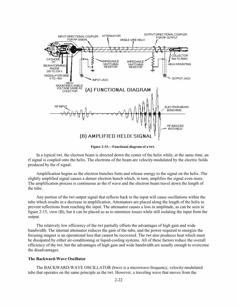
In a typical twt, the electron beam is directed down the center of the helix while, at the same time, an rf signal is coupled onto the helix. The electrons of the beam are velocity-modulated by the electric fields produced by the rf signal.
Amplification begins as the electron bunches form and release energy to the signal on the helix. The slightly amplified signal causes a denser electron bunch which, in turn, amplifies the signal even more. The amplification process is continuous as the rf wave and the electron beam travel down the length of the tube.
Any portion of the twt output signal that reflects back to the input will cause oscillations within the tube which results in a decrease in amplification. Attenuators are placed along the length of the helix to prevent reflections from reaching the input. The attenuator causes a loss in amplitude, as can be seen in figure 2-15, view (B), but it can be placed so as to minimize losses while still isolating the input from the output.
The relatively low efficiency of the twt partially offsets the advantages of high gain and wide bandwidth. The internal attenuator reduces the gain of the tube, and the power required to energize the focusing magnet is an operational loss that cannot be recovered. The twt also produces heat which must be dissipated by either air-conditioning or liquid-cooling systems. All of these factors reduce the overall efficiency of the twt, but the advantages of high gain and wide bandwidth are usually enough to overcome the disadvantages.
The Backward-Wave Oscillator
The BACKWARD-WAVE OSCILLATOR (bwo) is a microwave-frequency, velocity-modulated tube that operates on the same principle as the twt. However, a traveling wave that moves from the

2-23
electron gun end of the tube toward the collector is not used in the bwo. Instead, the bwo extracts energy from the electron. beam by using a backward wave that travels from the collector toward the electron gun (cathode). Otherwise, the electron bunching action and energy extraction from the electron beam is very similar to the actions in a twt.
The typical bwo is constructed from a folded transmission line or waveguide that winds back and forth across the path of the electron beam, as shown in figure 2-16. The folded waveguide in the illustration serves the same purpose as the helix in a twt. The fixed spacing of the folded waveguide limits the bandwidth of the bwo. Since the frequency of a given waveguide is constant, the frequency of the bwo is controlled by the transit time of the electron beam. The transit time is controlled by the collector potential. Thus, the output frequency can be changed by varying the collector voltage, which is a definite advantage. As in the twt, the electron beam in the bwo is focused by a magnet placed around the body of the tube.
Figure 2-16.—Typical bwo.
Q-26. What is the primary use of the twt?
Q-27. The magnet surrounding the body of a twt serves what purpose?
Q-28. How are the input and output directional couplers in a twt connected to the helix?
Q-29. What relationship must exist between the electron beam and the traveling wave for bunching to occur in the electron beam of a twt?
Q-30. What structure in the twt delays the forward progress of the traveling wave?
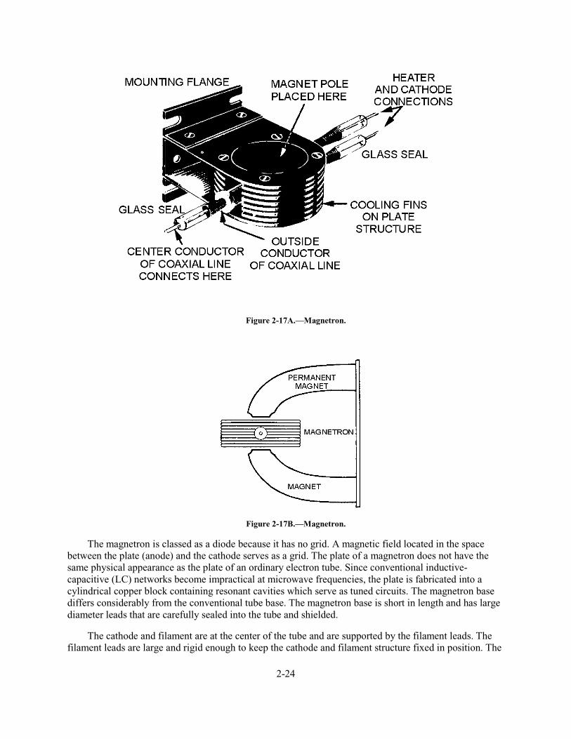
The Magnetron
The MAGNETRON, shown in figure 2-17A, is a self-contained microwave oscillator that operates differently from the linear-beam tubes, such as the twt and the klystron. Figure 2-17B is a simplified drawing of the magnetron. CROSSED-ELECTRON and MAGNETIC fields are used in the magnetron to produce the high-power output required in radar and communications equipment.
2-24
Figure 2-17A.—Magnetron.
Figure 2-17B.—Magnetron.
The magnetron is classed as a diode because it has no grid. A magnetic field located in the space between the plate (anode) and the cathode serves as a grid. The plate of a magnetron does not have the same physical appearance as the plate of an ordinary electron tube. Since conventional inductive-capacitive (LC) networks become impractical at microwave frequencies, the plate is fabricated into a cylindrical copper block containing resonant cavities which serve as tuned circuits. The magnetron base differs considerably from the conventional tube base. The magnetron base is short in length and has large diameter leads that are carefully sealed into the tube and shielded.
The cathode and filament are at the center of the tube and are supported by the filament leads. The filament leads are large and rigid enough to keep the cathode and filament structure fixed in position. The

2-25
output lead is usually a probe or loop extending into one of the tuned cavities and coupled into a waveguide or coaxial line. The plate structure, shown in figure 2-18, is a solid block of copper. The cylindrical holes around its circumference are resonant cavities. A narrow slot runs from each cavity into the central portion of the tube dividing the inner structure into as many segments as there are cavities. Alternate segments are strapped together to put the cavities in parallel with regard to the output. The cavities control the output frequency. The straps are circular, metal bands that are placed across the top of the block at the entrance slots to the cavities. Since the cathode must operate at high power, it must be fairly large and must also be able to withstand high operating temperatures. It must also have good emission characteristics, particularly under return bombardment by the electrons. This is because most of the output power is provided by the large number of electrons that are emitted when high-velocity electrons return to strike the cathode. The cathode is indirectly heated and is constructed of a high-emission material. The open space between the plate and the cathode is called the INTERACTION SPACE. In this space the electric and magnetic fields interact to exert force upon the electrons.
Figure 2-18.—Cutaway view of a magnetron.
The magnetic field is usually provided by a strong, permanent magnet mounted around the magnetron so that the magnetic field is parallel with the axis of the cathode. The cathode is mounted in the center of the interaction space.
BASIC MAGNETRON OPERATION.—Magnetron theory of operation is based on the motion of electrons under the influence of combined electric and magnetic fields. The following information presents the laws governing this motion.
The direction of an electric field is from the positive electrode to the negative electrode. The law governing the motion of an electron in an electric field (E field) states:
The force exerted by an electric field on an electron is proportional to the strength of the field. Electrons tend to move from a point of negative potential toward a positive potential.
CATHODE
PICKUPLOOP
OUTER CONDUCTOROF COAXIAL LINE
COOLING FINS
RESONANT CAVITIES
GLASS SEAL
CATHODEAND FILAMENT LEAD
INTERACTIONSPACEALTERNATE SEGMENTS OF
PLATE STRAPPED TOGETHER
CENTER CONDUCTOROF COAXIAL LINE
GLASS SEAL
NTS110218
MOUNTING FLANGE

2-26
This is shown in figure 2-19. In other words, electrons tend to move against the E field. When an electron is being accelerated by an E field, as shown in figure 2-19, energy is taken from the field by the electron.
Figure 2-19.—Electron motion in an electric field.
The law of motion of an electron in a magnetic field (H field) states:
The force exerted on an electron in a magnetic field is at right angles to both the field and the path of the electron. The direction of the force is such that the electron trajectories are clockwise when viewed in the direction of the magnetic field.
This is shown in figure 2-20.
Figure 2-20.—Electron motion in a magnetic field.
In figure 2-20, assume that a south pole is below the figure and a north pole is above the figure so that the magnetic field is going into the paper. When an electron is moving through space, a magnetic field builds around the electron just as it would around a wire when electrons are flowing through a wire. In figure 2-20 the magnetic field around the moving electron adds to the permanent magnetic field on the

2-27
left side of the electron's path and subtracts from the permanent magnetic field on the right side. This action weakens the field on the right side; therefore, the electron path bends to the right (clockwise). If the strength of the magnetic field is increased, the path of the electron will have a sharper bend. Likewise, if the velocity of the electron increases, the field around it increases and the path will bend more sharply.
A schematic diagram of a basic magnetron is shown in figure 2-21A. The tube consists of a cylindrical plate with a cathode placed along the center axis of the plate. The tuned circuit is made up of cavities in which oscillations take place and are physically located in the plate.
When no magnetic field exists, heating the cathode results in a uniform and direct movement of the field from the cathode to the plate, as illustrated in figure 2-21B. However, as the magnetic field surrounding the tube is increased, a single electron is affected, as shown in figure 2-22. In figure 2-22, view (A), the magnetic field has been increased to a point where the electron proceeds to the plate in a curve rather than a direct path.
Figure 2-21A.—Basic magnetron. SIDE VIEW.
Figure 2-21B.—Basic magnetron. END VIEW OMITTING MAGNETS.

2-28
Figure 2-22.—Effect of a magnetic field on a single electron.
In view (B) of figure 2-22, the magnetic field has reached a value great enough to cause the electron to just miss the plate and return to the filament in a circular orbit. This value is the CRITICAL VALUE of field strength. In view (C), the value of the field strength has been increased to a point beyond the critical value; the electron is made to travel to the cathode in a circular path of smaller diameter.
View (D) of figure 2-22. shows how the magnetron plate current varies under the influence of the varying magnetic field. In view (A), the electron flow reaches the plate, so a large amount of plate current is flowing. However, when the critical field value is reached, as shown in view (B), the electrons are deflected away from the plate and the plate current then drops quickly to a very small value. When the field strength is made still greater, as shown in view (C), the plate current drops to zero.
When the magnetron is adjusted to the cutoff, or critical value of the plate current, and the electrons just fail to reach the plate in their circular motion, it can produce oscillations at microwave frequencies. These oscillations are caused by the currents induced electrostatically by the moving electrons. The frequency is determined by the time it takes the electrons to travel from the cathode toward the plate and back again. A transfer of microwave energy to a load is made possible by connecting an external circuit between the cathode and the plate of the magnetron. Magnetron oscillators are divided into two classes: NEGATIVE-RESISTANCE and ELECTRON-RESONANCE MAGNETRON OSCILLATORS.
A negative-resistance magnetron oscillator is operated by a static negative resistance between its electrodes. This oscillator has a frequency equal to the frequency of the tuned circuit connected to the tube.
An electron-resonance magnetron oscillator is operated by the electron transit time required for electrons to travel from cathode to plate. This oscillator is capable of generating very large peak power outputs at frequencies in the thousands of megahertz. Although its average power output over a period of time is low, it can provide very high-powered oscillations in short bursts of pulses.
Q-31. The folded waveguide in a bwo serves the same purpose as what component in a twt?
NTS110222
PLATE CATHODE
A B C
END VIEW OF MAGNETRON
PL
AT
EC
UR
RE
NT
MAGNETIC FIELD STRENGTH CRITICAL VALUE OFFIELD STRENGTH
D

2-29
Q-32. What serves as a grid in a magnetron?
Q-33. A cylindrical copper block with resonant cavities around the circumference is used as what component of a magnetron?
Q-34. What controls the output frequency of a magnetron?
Q-35. What element in the magnetron causes the curved path of electron flow?
Q-36. What is the term used to identify the amount of field strength required to cause the electrons to just miss the plate and return to the filament in a circular orbit?
Q-37. A magnetron will produce oscillations when the electrons follow what type of path?
NEGATIVE-RESISTANCE MAGNETRON.—The split-anode, negative-resistance magnetron is a variation of the basic magnetron which operates at a higher frequency. The negative-resistance magnetron is capable of greater power output than the basic magnetron. Its general construction is similar to the basic magnetron except that it has a split plate, as shown in figure 2-23A and B. These half plates are operated at different potentials to provide an electron motion, as shown in figure 2-24. The electron leaving the cathode and progressing toward the high-potential plate is deflected by the magnetic field and follows the path shown in figure 2-24. After passing the split between the two plates, the electron enters the electrostatic field set up by the lower-potential plate.
Figure 2-23A.—Split-anode magnetron.

2-30
Figure 2-23B.—Split-anode magnetron.
Figure 2-24.—Movement of an electron in a split-anode magnetron.
Here the magnetic field has more effect on the electron and deflects it into a tighter curve. The electron then continues to make a series of loops through the magnetic field and the electric field until it finally arrives at the low-potential plate.
Oscillations are started by applying the proper magnetic field to the tube. The field value required is slightly higher than the critical value. In the split-anode tube, the critical value is the field value required to cause all the electrons to miss the plate when its halves are operating at the same potential. The alternating voltages impressed on the plates by the oscillations generated in the tank circuit will cause electron motion, such as that shown in figure 2-24, and current will flow. Since a very concentrated magnetic field is required for the negative-resistance magnetron oscillator, the length of the tube plate is limited to a few centimeters to keep the magnet at reasonable dimensions. In addition, a small diameter tube is required to make the magnetron operate efficiently at microwave frequencies. A heavy-walled plate is used to increase the radiating properties of the tube. Artificial cooling methods, such as forced-air or water-cooled systems, are used to obtain still greater dissipation in these high-output tubes.

2-31
The output of a magnetron is reduced by the bombardment of the filament by electrons which travel in loops, shown in figure 2-22, views (B) and (C). This action causes an increase of filament temperature under conditions of a strong magnetic field and high plate voltage and sometimes results in unstable operation of the tube. The effects of filament bombardment can be reduced by operating the filament at a reduced voltage. In some cases, the plate voltage and field strength are also reduced to prevent destructive filament bombardment.
ELECTRON-RESONANCE MAGNETRON.—In the electron-resonance magnetron, the plate is constructed to resonate and function as a tank circuit. Thus, the magnetron has no external tuned circuits. Power is delivered directly from the tube through transmission lines, as shown in figure 2-25. The constants and operating conditions of the tube are such that the electron paths are somewhat different from those in figure 2-24. Instead of closed spirals or loops, the path is a curve having a series of sharp points, as illustrated in figure 2-26. Ordinarily, this type of magnetron has more than two segments in the plate. For example, figure 2-26 illustrates an eight-segment plate.
Figure 2-25.—Plate tank circuit of a magnetron.
Figure 2-26.—Electron path in an electron-resonance magnetron.
The electron-resonance magnetron is the most widely used for microwave frequencies because it has reasonably high efficiency and relatively high output. The average power of the electron-resonance magnetron is limited by the amount of cathode emission, and the peak power is limited by the maximum voltage rating of the tube components. Three common types of anode blocks used in electron-resonance magnetrons are shown in figure 2-27.

2-32
Figure 2-27.—Common types of anode blocks.
The anode block shown in figure 2-27, view (A), has cylindrical cavities and is called a HOLE-AND-SLOT ANODE. The anode block in view (B) is called the VANE ANODE which has trapezoidal cavities. The first two anode blocks operate in such a way that alternate segments must be connected, or strapped, so that each segment is opposite in polarity to the segment on either side, as shown in figure 2-28. This also requires an even number of cavities.
Figure 2-28.—Strapping alternate segments.
The anode block illustrated in figure 2-27, view (C), is called a RISING-SUN BLOCK. The alternate large and small trapezoidal cavities in this block result in a stable frequency between the resonant frequencies of the large and small cavities.
Figure 2-29A, shows the physical relationships of the resonant cavities contained in the hole-and-slot anode (figure 2-27, view (A)). This will be used when analyzing the operation of the electron-resonance magnetron.

2-33
Figure 2-29A.—Equivalent circuit of a hole-and-slot cavity.
Figure 2-29B.—Equivalent circuit of a hole-and-slot cavity.
Electrical Equivalent.—Notice in figure 2-29A, that the cavity consists of a cylindrical hole in the copper anode and a slot which connects the cavity to the interaction space.
The equivalent electrical circuit of the hole and slot is shown in figure 2-29B. The parallel sides of the slot form the plates of a capacitor while the walls of the hole act as an inductor. The hole and slot thus form a high-Q, resonant LC circuit. As shown in figure 2-27, the anode of a magnetron has a number of these cavities.
An analysis of the anodes in the hole-and-slot block reveals that the LC tanks of each cavity are in series (assuming the straps have been removed), as shown in figure 2-30. However, an analysis of the anode block after alternate segments have been strapped reveals that the cavities are connected in parallel because of the strapping. Figure 2-31 shows the equivalent circuit of a strapped anode.
Figure 2-30.—Cavities connected in series.

2-34
Figure 2-31.—Cavities in parallel because of strapping.
Electric Field.—The electric field in the electron-resonance oscillator is a product of ac and dc fields. The dc field extends radially from adjacent anode segments to the cathode, as shown in figure 2-32. The ac fields, extending between adjacent segments, are shown at an instant of maximum magnitude of one alternation of the rf oscillations occurring in the cavities.
Figure 2-32.—Probable electron paths in an electron-resonance magnetron oscillator.
The strong dc field going from anode to cathode is created by a large, negative dc voltage pulse applied to the cathode. This strong dc field causes electrons to accelerate toward the plate after they have been emitted from the cathode. Recall that an electron moving against an E field is accelerated by the field and takes energy from the field. Also, an electron gives up energy to a field and slows down if it is moving in the same direction as the field (positive to negative). Oscillations are sustained in a magnetron because as electrons pass through the ac and dc fields, they gain energy from the dc field and give up energy to the ac field. The electrons that give up energy to the ac field are called WORKING ELECTRONS. However, not all of the electrons give up energy to the ac field. Some electrons take energy from the ac field, which is an undesirable action.
In figure 2-32, consider electron Q1, which is shown entering the field around the slot entrance to cavity A. The clockwise rotation of the electron path is caused by the interaction of the magnetic field around the moving electron with the permanent magnetic field. The permanent magnetic field is assumed to be going into the paper in figure 2-32 (the action of an electron moving in an H field was explained
2-35
earlier). Notice that electron Q1 is moving against the ac field around cavity A. The electron takes energy from the ac field and then accelerates, turning more sharply when its velocity increases. Thus, electron Q1 turns back toward the cathode. When it strikes the cathode, it gives up the energy it received from the ac field. This bombardment also forces more electrons to leave the cathode and accelerate toward the anode. Electron Q2 is slowed down by the field around cavity B and gives up some of its energy to the ac field. Since electron Q2 loses velocity, the deflective force exerted by the H field is reduced. The electron path then deviates to the left in the direction of the anode, rather than returning to the cathode as did electron Q1.
The cathode to anode potential and the magnetic field strength determine the amount of time for electron Q2 to travel from a position in front of cavity B to a position in front of cavity C. Cavity C is equal to approximately 1/2 cycle of the rf oscillations of the cavities. When electron Q2 reaches a position in front of cavity C, the ac field of cavity C is reversed from that shown. Therefore, electron Q2 gives up energy to the ac field of cavity C and slows down even more. Electron Q2 actually gives up energy to each cavity as it passes and eventually reaches the anode when its energy is expended. Thus, electron Q2 has helped sustain oscillations because it has taken energy from the dc field and given it to the ac field. Electron Q1, which took energy from the ac field around cavity A, did little harm because it immediately returned to the cathode.
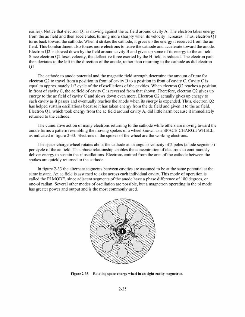
The cumulative action of many electrons returning to the cathode while others are moving toward the anode forms a pattern resembling the moving spokes of a wheel known as a SPACE-CHARGE WHEEL, as indicated in figure 2-33. Electrons in the spokes of the wheel are the working electrons.
The space-charge wheel rotates about the cathode at an angular velocity of 2 poles (anode segments) per cycle of the ac field. This phase relationship enables the concentration of electrons to continuously deliver energy to sustain the rf oscillations. Electrons emitted from the area of the cathode between the spokes are quickly returned to the cathode.
In figure 2-33 the alternate segments between cavities are assumed to be at the same potential at the same instant. An ac field is assumed to exist across each individual cavity. This mode of operation is called the PI MODE, since adjacent segments of the anode have a phase difference of 180 degrees, or one-pi radian. Several other modes of oscillation are possible, but a magnetron operating in the pi mode has greater power and output and is the most commonly used.
Figure 2-33.—Rotating space-charge wheel in an eight-cavity magnetron.

2-36
An even number of cavities, usually six or eight, are used and alternate segments are strapped to ensure that they have identical polarities. The frequency of the pi mode is separated from the frequency of the other modes by strapping.
For the pi mode, all parts of each strapping ring are at the same potential; but the two rings have alternately opposing potentials, as shown in figure 2-34. Stray capacitance between the rings adds capacitive loading to the resonant mode. For other modes, however, a phase difference exists between the successive segments connected to a given strapping ring which causes current to flow in the straps.
Figure 2-34.—Alternate segments connected by strapping rings.
The straps contain inductance, and an inductive shunt is placed in parallel with the equivalent circuit. This lowers the inductance and increases the frequency at modes other than the pi mode.
Q-38. What is the primary difference in construction between the basic magnetron and the negative-resistance magnetron?
Q-39. What starts the oscillations in a negative-resistance magnetron?
Q-40. Why is the negative-resistance magnetron often operated with reduced filament voltage?
Q-41. What type of electron-resonance anode block does not require strapping?
Q-42. Without strapping, the resonant cavities of a hole-and-slot anode are connected in what manner?
Q-43. What are the electrons called that give up energy to the ac field in a magnetron?
COUPLING METHODS.—Energy (rf) can be removed from a magnetron by means of a COUPLING LOOP. At frequencies lower than 10,000 megahertz, the coupling loop is made by bending the inner conductor of a coaxial cable into a loop. The loop is then soldered to the end of the outer conductor so that it projects into the cavity, as shown in figure 2-35A. Locating the loop at the end of the cavity, as shown in figure 2-35B, causes the magnetron to obtain sufficient pickup at higher frequencies.

2-37
Figure 2-35A.—Magnetron coupling methods.
Figure 2-35B.—Magnetron coupling methods.
The SEGMENT-FED LOOP METHOD is shown in figure 2-35C. The loop intercepts the magnetic lines passing between cavities. The STRAP-FED LOOP METHOD (figure 2-35D), intercepts the energy between the strap and the segment. On the output side, the coaxial line feeds another coaxial line directly or feeds a waveguide through a choke joint. The vacuum seal at the inner conductor helps to support the line. APERTURE, OR SLOT, COUPLING is illustrated in figure 2-35E. Energy is coupled directly to a waveguide through an iris.
Figure 2-35C.—Magnetron coupling methods.

2-38
Figure 2-35D.—Magnetron coupling methods.
Figure 2-35E.—Magnetron coupling methods.
MAGNETRON TUNING.—A tunable magnetron permits the system to be operated at a precise frequency anywhere within a band of frequencies, as determined by magnetron characteristics.
The resonant frequency of a magnetron may be changed by varying the inductance or capacitance of the resonant cavities. In figure 2-36, an inductive tuning element is inserted into the hole portion of the hole-and-slot cavities. It changes the inductance of the resonant circuits by altering the ratio of surface area to cavity volume in a high-current region. The type of tuner illustrated in figure 2-36 is called a SPROCKET TUNER or CROWN-OF-THORNS TUNER. All of its tuning elements are attached to a frame which is positioned by a flexible bellows arrangement. The insertion of the tuning elements into each anode hole decreases the inductance of the cavity and therefore increases the resonant frequency. One of the limitations of inductive tuning is that it lowers the unloaded Q of the cavities and therefore reduces the efficiency of the tube.

2-39
Figure 2-36.—Inductive magnetron tuning.
The insertion of an element (ring) into the cavity slot, as shown in figure 2-37, increases the slot capacitance and decreases the resonant frequency. Because the gap is narrowed in width, the breakdown voltage is lowered. Therefore, capacitively tuned magnetrons must be operated with low voltages and at low-power outputs. The type of capacitive tuner illustrated in figure 2-37 is called a COOKIE-CUTTER TUNER. It consists of a metal ring inserted between the two rings of a double-strapped magnetron, which serves to increase the strap capacitance. Because of the mechanical and voltage breakdown problems associated with the cookie-cutter tuner, it is more suitable for use at longer wavelengths. Both the capacitance and inductance tuners described are symmetrical; that is, each cavity is affected in the same manner, and the pi mode is preserved.
Figure 2-37.—Capacitive magnetron tuning.

2-40
A 10-percent frequency range may be obtained with either of the two tuning methods described above. Also, the two tuning methods may be used in combination to cover a larger tuning range than is possible with either one alone.
ARCING IN MAGNETRONS.—During initial operation a high-powered magnetron arcs from cathode to plate and must be properly BROKEN IN or BAKED IN. Actually, arcing in magnetrons is very common. It occurs with a new tube or following long periods of idleness.
One of the prime causes of arcing is the release of gas from tube elements during idle periods. Arcing may also be caused by the presence of sharp surfaces within the tube, mode shifting, and by drawing excessive current. While the cathode can withstand considerable arcing for short periods of time, continued arcing will shorten the life of the magnetron and may destroy it entirely. Therefore, each time excessive arcing occurs, the tube must be baked in again until the arcing ceases and the tube is stabilized.
The baking-in procedure is relatively simple. Magnetron voltage is raised from a low value until arcing occurs several times a second. The voltage is left at that value until arcing dies out. Then the voltage is raised further until arcing again occurs and is left at that value until the arcing again ceases. Whenever the arcing becomes very violent and resembles a continuous arc, the applied voltage is excessive and should be reduced to permit the magnetron to recover. When normal rated voltage is reached and the magnetron remains stable at the rated current, the baking-in is complete. A good maintenance practice is to bake-in magnetrons left idle in the equipment or those used as spares when long periods of nonoperating time have accumulated.
The preceding information is general in nature. The recommended times and procedures in the technical manuals for the equipment should be followed when baking-in a specific type magnetron.
The Crossed-Field Amplifier (Amplitron)
The CROSSED-FIELD AMPLIFIER (cfa), commonly known as an AMPLITRON and sometimes referred to as a PLATINOTRON, is a broadband microwave amplifier that can also be used as an oscillator. The cfa is similar in operation to the magnetron and is capable of providing relatively large amounts of power with high efficiency. The bandwidth of the cfa, at any given instant, is approximately plus or minus 5 percent of the rated center frequency. Any incoming signals within this bandwidth are amplified. Peak power levels of many megawatts and average power levels of tens of kilowatts average are, with efficiency ratings in excess of 70 percent, possible with crossed-field amplifiers.
Because of the desirable characteristics of wide bandwidth, high efficiency, and the ability to handle large amounts of power, the cfa is used in many applications in microwave electronic systems. This high efficiency has made the cfa useful for space-telemetry applications, and the high power and stability have made it useful in high-energy, linear atomic accelerators. When used as the intermediate or final stage in high-power radar systems, all of the advantages of the cfa are used.
Since the cfa operates in a manner so similar to the magnetron, the detailed theory is not presented in this module. Detailed information of cfa operation is available in NAVSHIPS 0967-443-2230, Handling, Installation and Operation of Crossed-Field Amplifiers. As mentioned earlier, crossed-field amplifiers are commonly called Amplitrons. You should note, however, that Amplitron is a trademark of the Raytheon Manufacturing Company for the Raytheon line of crossed-field amplifiers. An illustration of a crossed-field amplifier is shown in figure 2-38.

2-41
Figure 2-38.—Crossed-field amplifier (Amplitron).
Q-44. Why is the pi mode the most commonly used magnetron mode of operation?
Q-45. What two methods are used to couple energy into and out of magnetrons?
Q-46. Magnetron tuning by altering the surface-to-volume ratio of the hole portion of a hole-and-slot cavity is what type of tuning?
Q-47. Capacitive tuning by inserting a ring into the cavity slot of a magnetron is accomplished by what type of tuning mechanism?
SOLID-STATE MICROWAVE DEVICES
As with vacuum tubes, the special electronics effects encountered at microwave frequencies severely limit the usefulness of transistors in most circuit applications. The need for small-sized microwave devices has caused extensive research in this area. This research has produced solid-state devices with higher and higher frequency ranges. The new solid-state microwave devices are predominantly active, two-terminal diodes, such as tunnel diodes, varactors, transferred-electron devices, and avalanche transit-time diodes. This section will describe the basic theory of operation and some of the applications of these relatively new solid-state devices.
Tunnel Diode Devices
The TUNNEL DIODE is a pn junction with a very high concentration of impurities in both the p and n regions. The high concentration of impurities causes it to exhibit the properties of a negative-resistance element over part of its range of operation, as shown in the characteristic curve in figure 2-39. In other words, the resistance to current flow through the tunnel diode increases as the applied voltage increases over a portion of its region of operation. Outside the negative-resistance region, the tunnel diode functions essentially the same as a normal diode. However, the very high impurity density causes a junction depletion region so narrow that both holes and electrons can transfer across the pn junction by a quantum

2-42
mechanical action called TUNNELING. Tunneling causes the negative-resistance action and is so fast that no transit-time effects occur even at microwave frequencies. The lack of a transit-time effect permits the use of tunnel diodes in a wide variety of microwave circuits, such as amplifiers, oscillators, and switching devices. The detailed theory of tunnel-diode operation and the negative-resistance property exhibited by the tunnel diode was discussed in NEETS, Module 7, Introduction to Solid-State Devices and Power Supplies, Chapter 3.
Figure 2-39.—Tunnel-diode characteristic curve.
TUNNEL-DIODE OSCILLATORS.—A tunnel diode, biased at the center point of the negative-resistance range (point B in figure 2-39) and coupled to a tuned circuit or cavity, produces a very stable oscillator. The oscillation frequency is the same as the tuned circuit or cavity frequency.
Microwave tunnel-diode oscillators are useful in applications that require microwatts or, at most, a few milliwatts of power, such as local oscillators for microwave superheterodyne receivers. Tunnel-diode oscillators can be mechanically or electronically tuned over frequency ranges of about one octave and have a top-end frequency limit of approximately 10 gigahertz.
Tunnel-diode oscillators that are designed to operate at microwave frequencies generally use some form of transmission line as a tuned circuit. Suitable tuned circuits can be built from coaxial lines, transmission lines, and waveguides.
An example of a highly stable tunnel-diode oscillator is shown in figure 2-40. A tunnel-diode is loosely coupled to a high-Q tunable cavity. Loose coupling is achieved by using a short, antenna feed probe placed off-center in the cavity. Loose coupling is used to increase the stability of the oscillations and the output power over a wider bandwidth.

2-43
Figure 2-40.—Tunnel-diode oscillator.
The output power produced is in the range of a few hundred microwatts, sufficient for many microwave applications. The frequency at which the oscillator operates is determined by the physical positioning of the tuner screw in the cavity. Changing the output frequency by this method is called MECHANICAL TUNING. In addition to mechanical tuning, tunnel-diode oscillators may be tuned electronically. One method is called BIAS TUNING and involves nothing more than changing the bias voltage to change the bias point on the characteristic curve of the tunnel-diode. Another method is called VARACTOR TUNING and requires the addition of a varactor to the basic circuit. Varactors were discussed in NEETS, Module 7, Introduction to Solid-State Devices, and Power Supplies, Chapter 3. Tuning is achieved by changing the voltage applied across the varactor which alters the capacitance of the tuned circuit.
TUNNEL-DIODE AMPLIFIERS.—Low-noise, tunnel-diode amplifiers represent an important microwave application of tunnel diodes. Tunnel-diode amplifiers with frequencies up to 85 gigahertz have been built in waveguides, coaxial lines, and transmission lines. The low-noise generation, gain ratios of up to 30 dB, high reliability, and light weight make these amplifiers ideal for use as the first stage of amplification in communications and radar receivers.
Most microwave tunnel-diode amplifiers are REFLECTION-TYPE, CIRCULATOR-COUPLED AMPLIFIERS. As in oscillators, the tunnel diode is biased to the center point of its negative-resistance region, but a CIRCULATOR replaces the tuned cavity.
A circulator is a waveguide device that allows energy to travel in one direction only, as shown in figure 2-41. The tunnel diode in figure 2-41 is connected across a tuned-input circuit. This arrangement normally produces feedback that causes oscillations if the feedback is allowed to reflect back to the tuned-input circuit. The feedback is prevented because the circulator carries all excess energy to the absorptive load (R L). In this configuration the tunnel diode cannot oscillate, but will amplify.
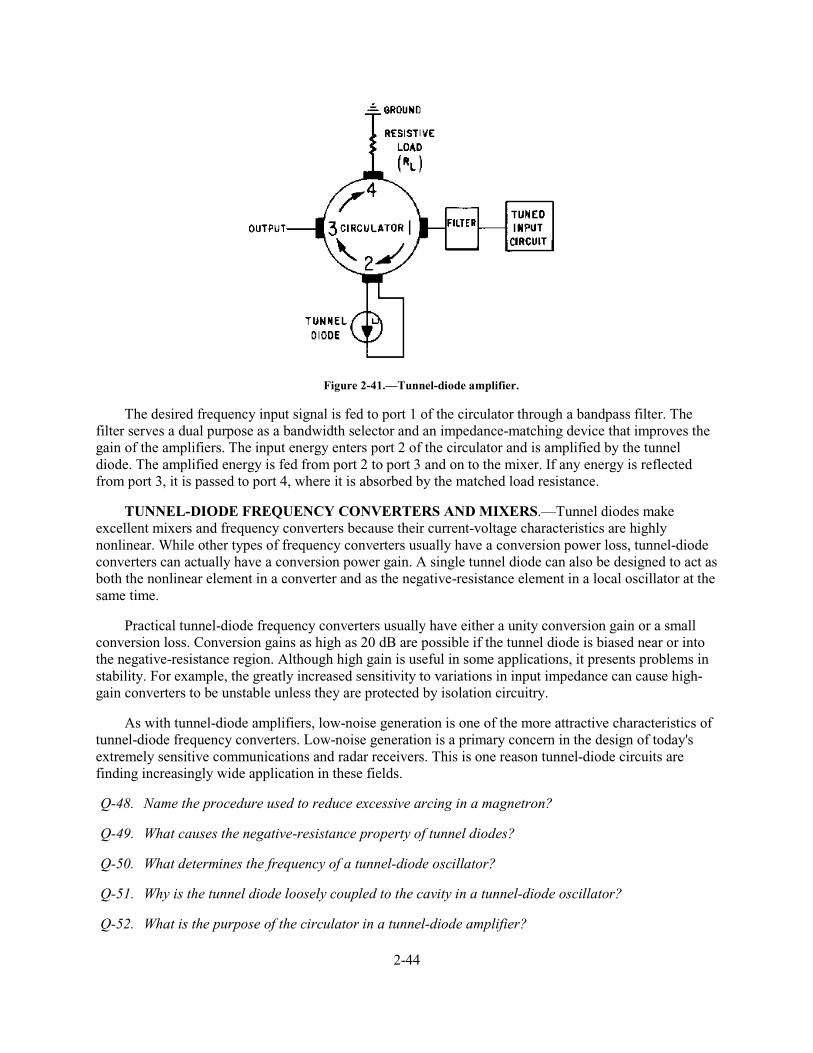
2-44
Figure 2-41.—Tunnel-diode amplifier.
The desired frequency input signal is fed to port 1 of the circulator through a bandpass filter. The filter serves a dual purpose as a bandwidth selector and an impedance-matching device that improves the gain of the amplifiers. The input energy enters port 2 of the circulator and is amplified by the tunnel diode. The amplified energy is fed from port 2 to port 3 and on to the mixer. If any energy is reflected from port 3, it is passed to port 4, where it is absorbed by the matched load resistance.
TUNNEL-DIODE FREQUENCY CONVERTERS AND MIXERS.—Tunnel diodes make excellent mixers and frequency converters because their current-voltage characteristics are highly nonlinear. While other types of frequency converters usually have a conversion power loss, tunnel-diode converters can actually have a conversion power gain. A single tunnel diode can also be designed to act as both the nonlinear element in a converter and as the negative-resistance element in a local oscillator at the same time.
Practical tunnel-diode frequency converters usually have either a unity conversion gain or a small conversion loss. Conversion gains as high as 20 dB are possible if the tunnel diode is biased near or into the negative-resistance region. Although high gain is useful in some applications, it presents problems in stability. For example, the greatly increased sensitivity to variations in input impedance can cause high-gain converters to be unstable unless they are protected by isolation circuitry.
As with tunnel-diode amplifiers, low-noise generation is one of the more attractive characteristics of tunnel-diode frequency converters. Low-noise generation is a primary concern in the design of today's extremely sensitive communications and radar receivers. This is one reason tunnel-diode circuits are finding increasingly wide application in these fields.
Q-48. Name the procedure used to reduce excessive arcing in a magnetron?
Q-49. What causes the negative-resistance property of tunnel diodes?
Q-50. What determines the frequency of a tunnel-diode oscillator?
Q-51. Why is the tunnel diode loosely coupled to the cavity in a tunnel-diode oscillator?
Q-52. What is the purpose of the circulator in a tunnel-diode amplifier?

2-45
Varactor Devices
The VARACTOR is another of the active two-terminal diodes that operates in the microwave range. Since the basic theory of varactor operation was presented in NEETS, Module 7, Introduction to Solid-State Devices and Power Supplies, Chapter 3, only a brief review of the basic principles is presented here.
The varactor is a semiconductor diode with the properties of a voltage-dependent capacitor. Specifically, it is a variable-capacitance, pn-junction diode that makes good use of the voltage dependency of the depletion-area capacitance of the diode.
In figure 2-42A, two materials are brought together to form a pn-junction diode. The different energy levels in the two materials cause a diffusion of the holes and electrons through both materials which tends to balance their energy levels. When this diffusion process stops, the diode is left with a small area on either side of the junction, called the depletion area, which contains no free electrons or holes. The movement of electrons through the materials creates an electric field across the depletion area that is described as a barrier potential and has the electrical characteristics of a charged capacitor.
Figure 2-42A.—Pn-junction diode as a variable capacitor.
External bias, applied in either the forward or reverse direction, as shown in figure 2-42B and C, affects the magnitude, barrier potential, and width of the depletion area. Enough forward or reverse bias will overcome the barrier potential and cause current to flow through the diode. The width of the depletion region can be controlled by keeping the bias voltage at levels that do not allow current flow. Since the depletion area acts as a capacitor, the diode will perform as a variable capacitor that changes with the applied bias voltage. The capacitance of a typical varactor can vary from 2 to 50 picofarads for a bias variation of just 2 volts.
Figure 2-42B.—Pn-junction diode as a variable capacitor.
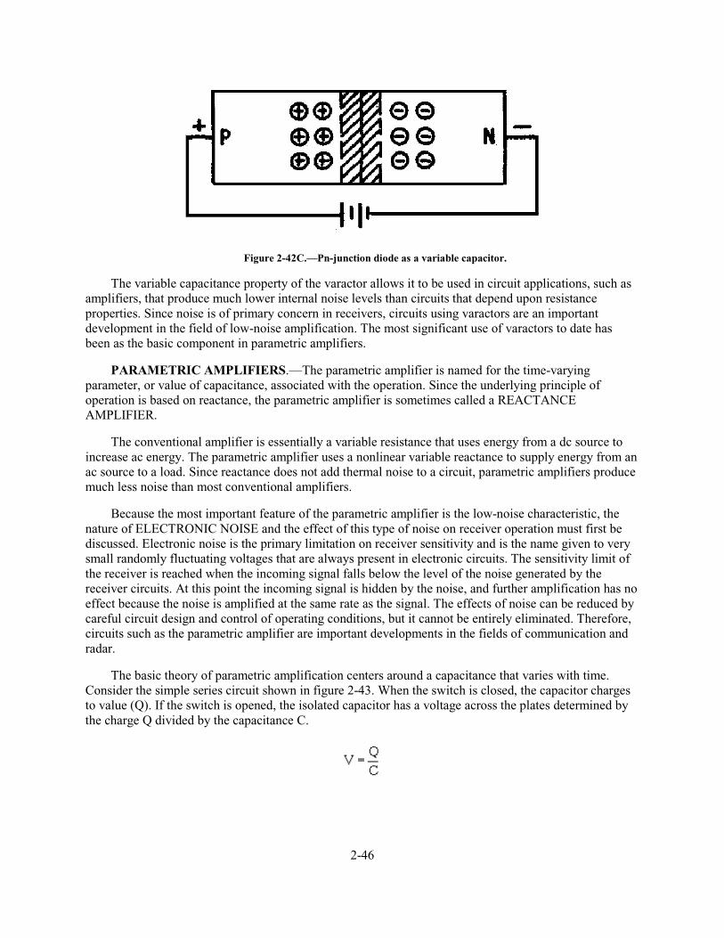
2-46
Figure 2-42C.—Pn-junction diode as a variable capacitor.
The variable capacitance property of the varactor allows it to be used in circuit applications, such as amplifiers, that produce much lower internal noise levels than circuits that depend upon resistance properties. Since noise is of primary concern in receivers, circuits using varactors are an important development in the field of low-noise amplification. The most significant use of varactors to date has been as the basic component in parametric amplifiers.
PARAMETRIC AMPLIFIERS.—The parametric amplifier is named for the time-varying parameter, or value of capacitance, associated with the operation. Since the underlying principle of operation is based on reactance, the parametric amplifier is sometimes called a REACTANCE AMPLIFIER.
The conventional amplifier is essentially a variable resistance that uses energy from a dc source to increase ac energy. The parametric amplifier uses a nonlinear variable reactance to supply energy from an ac source to a load. Since reactance does not add thermal noise to a circuit, parametric amplifiers produce much less noise than most conventional amplifiers.
Because the most important feature of the parametric amplifier is the low-noise characteristic, the nature of ELECTRONIC NOISE and the effect of this type of noise on receiver operation must first be discussed. Electronic noise is the primary limitation on receiver sensitivity and is the name given to very small randomly fluctuating voltages that are always present in electronic circuits. The sensitivity limit of the receiver is reached when the incoming signal falls below the level of the noise generated by the receiver circuits. At this point the incoming signal is hidden by the noise, and further amplification has no effect because the noise is amplified at the same rate as the signal. The effects of noise can be reduced by careful circuit design and control of operating conditions, but it cannot be entirely eliminated. Therefore, circuits such as the parametric amplifier are important developments in the fields of communication and radar.
The basic theory of parametric amplification centers around a capacitance that varies with time. Consider the simple series circuit shown in figure 2-43. When the switch is closed, the capacitor charges to value (Q). If the switch is opened, the isolated capacitor has a voltage across the plates determined by the charge Q divided by the capacitance C.
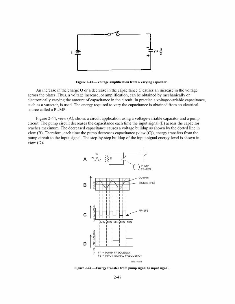
2-47
Figure 2-43.—Voltage amplification from a varying capacitor.
An increase in the charge Q or a decrease in the capacitance C causes an increase in the voltage across the plates. Thus, a voltage increase, or amplification, can be obtained by mechanically or electronically varying the amount of capacitance in the circuit. In practice a voltage-variable capacitance, such as a varactor, is used. The energy required to vary the capacitance is obtained from an electrical source called a PUMP.
Figure 2-44, view (A), shows a circuit application using a voltage-variable capacitor and a pump circuit. The pump circuit decreases the capacitance each time the input signal (E) across the capacitor reaches maximum. The decreased capacitance causes a voltage buildup as shown by the dotted line in view (B). Therefore, each time the pump decreases capacitance (view (C)), energy transfers from the pump circuit to the input signal. The step-by-step buildup of the input-signal energy level is shown in view (D).
Figure 2-44.—Energy transfer from pump signal to input signal.
OUTPUT
SIGNAL (FS)
VO
LT
S
B
CA
PA
CIT
AN
CE
C
FP=2FS
MIN MIN MIN MIN MIN
TO
TA
LTA
NK
EN
ER
GY
D
FP = PUMP FREQUENCYFS = INPUT SIGNAL FREQUENCY
A
PUMPFP=2FS
E
FS
NTS110244

2-48
Proper phasing between the pump and the input signal is crucial in this circuit. The electrical pump action is simply a sine-wave voltage applied to a varactor located in a resonant cavity. For proper operation, the capacitance must be decreased when the input voltage is maximum and increased when the input voltage is minimum. In other words, the pump signal frequency must be exactly double the frequency of the input signal. This relationship can be seen when you compare views (B) and (C). A parametric amplifier of the type shown in figure 2-44 is quite phase-sensitive. The input signal and the capacitor variation are often in the wrong phase for long periods of time.
A parametric amplifier that is not phase-sensitive, referred to as a NONDEGENERATIVE PARAMETRIC AMPLIFIER, uses a pump circuit with a frequency higher than twice the input signal. The higher-frequency pump signal mixes with the input signal and produces additional frequencies that represent both the sum and difference of the input signal and pump frequencies.
Figure 2-45A, is a diagram of a typical nondegenerative parametric amplifier with the equivalent circuit shown in figure 2-45B. The pump signal (fp) is applied to the varactor. The cavity on the left is resonant at the input frequency (fs), and the cavity on the right is resonant at the difference frequency (fp-fs). The difference frequency is called the IDLER- or LOWER-SIDEBAND frequency. The varactor is located at the high-voltage points of the two cavities and is reverse biased by a small battery. The pump signal varies the bias above and below the fixed-bias level.
Figure 2-45A.—Nondegenerative parametric amplifier. CIRCUIT.
NTS110245A
A. CIRCUIT
AMPLIFIEDFS SIGNAL
OUTPUT
DUMMYLOAD
(UNUSEDPORT)
FERRITECIRCULATOR
FS INPUT3 GHz
FS3 GHz
FP-FS9 GHz
vv
v
vv v
SIGNALCAVITY
SIGNAL INPUT
FSINPUT
FSOUTPUT
IDLERCAVITY
VARACTORDIODEREVERSE-
BIAS BATTERY
FP PUMP 12 GHz

2-49
Figure 2-45B.—Nondegenerative parametric amplifier. ELECTRICAL EQUIVALENT.
The pump signal causes the capacitor in figure 2-45A to vary at a 12-gigahertz rate. The 3-gigahertz input signal enters via a four-port ferrite circulator, is developed in the signal cavity, and applied across the varactor. The nonlinear action of the varactor produces a 9-gigahertz difference frequency (fp-fs) with an energy-level higher than the original input signal.
The difference (idler) frequency is reapplied to the varactor to increase the gain and to produce an output signal of the correct frequency. The 9-gigahertz idler frequency recombines with the 12-gigahertz pump signal and produces a 3-gigahertz difference signal that has a much larger amplitude than the original 3-gigahertz input signal. The amplified signal is sent to the ferrite circulator for transfer to the next stage.
As with tunnel-diode amplifiers, the circulator improves stability by preventing reflection of the signal back into the amplifier. Reflections would be amplified and cause uncontrollable oscillations. The ferrite circulator also serves as an isolator to prevent source and load impedance changes from affecting gain.
Typically, the gain of a parametric amplifier is about 20 dB. The gain can be controlled with a variable attenuator that changes the amount of pump power applied to the varactor.
Parametric amplifiers are relatively simple in construction. The only component is a varactor diode placed in an arrangement of cavities and waveguides. The most elaborate feature of the amplifier is the mechanical tuning mechanism. Figure 2-46 illustrates an actual parametric amplifier.
AMPLIFIEDFS SIGNAL
OUTPUT
DUMMYLOAD
(UNUSEDPORT)
FERRITECIRCULATOR
FS INPUT
FP-FS
vv
v
vv
v
FS
SIGNALTANK3 GHz
FP PUMP 12 GHzSIGNAL INPUT
IDLERTANK9 GHz
FS INPUTAND
OUTPUT3 GHz
VOLTAGE CONROLLEDCAPACITOR (VARACTOR)
NTS110245B
B. ELECTRICAL EQUIVALENT

2-50
Figure 2-46.—Parametric amplifier.
PARAMETRIC FREQUENCY CONVERTERS.—Parametric frequency converters, using varactors, are of three basic types. The UPPER-SIDEBAND PARAMETRIC UP-CONVERTER produces an output frequency that is the SUM of the input frequency and the pump frequency. The LOWER-SIDEBAND PARAMETRIC DOWN-CONVERTER produces an output frequency that is the DIFFERENCE between the pump frequency and the input frequency. The DOUBLE-SIDEBAND PARAMETRIC UP-CONVERTER produces an output in which both the SUM and the DIFFERENCE of the pump and input frequencies are available.
Parametric frequency converters are very similar to parametric amplifiers in both construction and operation. Figure 2-47 is a functional diagram of a parametric down-converter.
The parametric frequency converter operates in the same manner as the parametric amplifier except that the sideband frequencies are not reapplied to the varactor. Therefore, the output is one or both of the sideband frequencies and is not the same as the input frequency. The output frequency is determined by the cavity used as an output. For example, the idler cavity in figure 2-47 could be replaced by a cavity that is resonant at the upper-sideband frequency (22 gigahertz) to produce an upper-sideband parametric up-converter. Since input and output signals are at different frequencies, the parametric frequency converter does not require a ferrite circulator. However, a ferrite isolator is used to isolate the converter from changes in source impedance.
Figure 2-47.—Lower-sideband parametric down-converter.
NTS110247
SIGNAL CAVITY
SIGNAL INPUT IDLER
CAVITY
IDLER
OUTPUT
VARACTOR
DIODEREVERSE-BIAS
BATTERY
FP PUMP
FS INPUT
FROM
ANTENNA
FE
RR
ITE
ISO
LA
TE
R 10
GHz
12 GHz
2 GHzFS FP-FS

2-51
Q-53. What limits the usefulness of high-gain, tunnel-diode frequency converters?
Q-54. The varactor is a pn junction that acts as what type of electronic device?
Q-55. The underlying principle of operation of the parametric amplifier is based on what property?
Q-56. What is the most important feature of the parametric amplifier?
Q-57. How is amplification achieved in the circuit shown in figure 2-43?
Q-58. What is the purpose of the pump in a parametric amplifier?
Q-59. The pump signal frequency must be of what value when compared to the input signal of a simple parametric amplifier?
Q-60. What is the primary difference between the pump signal of a simple parametric amplifier and the pump signal of a nondegenerative parametric amplifier?
Q-61. In a nondegenerative parametric amplifier the difference between the input frequency and the pump frequency is called what?
Bulk-Effect Semiconductors
BULK-EFFECT SEMICONDUCTORS are unlike normal pn-junction diodes in both construction and operation. Some types have no junctions and the processes necessary for operation occur in a solid block of semiconductor material. Other types have more than one junction but still use bulk-effect action. Bulk-effect devices are among the latest of developments in the field of microwave semiconductors and new applications are being developed rapidly. They seem destined to revolutionize the field of high-power, solid-state microwave generation because they can produce much larger microwave power outputs than any currently available pn-junction semiconductors.
Bulk-effect semiconductors are of two basic types: the transferred-electron devices and the avalanche transit-time devices.
TRANSFERRED-ELECTRON SEMICONDUCTORS.—The discovery that microwaves could be generated by applying a steady voltage across a chip of n-type gallium-arsenide (GaAs) crystal was made in 1963 by J.B. Gunn. The device is operated by raising electrons in the crystal to conduction-band energy levels that are higher than the level they normally occupy. The overall effect is called the transferred-electron effect.
In a gallium-arsenide semiconductor, empty electron conduction bands exist that are at a higher energy level than the conduction bands occupied by most of the electrons. Any electrons that do occupy the higher conduction band essentially have no mobility. If an electric field of sufficient intensity is applied to the semiconductor electrons, they will move from the low-energy conduction band to the high-energy conduction band and become essentially immobile. The immobile electrons no longer contribute to the current flow and the applied voltage progressively increases the rate at which the electrons move from the low band to the high band. As the curve in figure 2-48 shows, the maximum current rate is reached and begins to decrease even though the applied voltage continues to increase. The point at which the current on the curve begins to decrease is called the THRESHOLD. This point is the beginning of the negative-resistance region. Negative resistance is caused by electrons moving to the higher conduction band and becoming immobile.

2-52
Figure 2-48.—Characteristic curve for a bulk-effect semiconductor.
If an increase in voltage is applied to a gallium-arsenide semiconductor, which is biased to operate in the negative-resistance region, it divides into regions of varying electric fields. A tiny region, known as a DOMAIN, forms that has an electric field of much greater intensity than the fields in the rest of the semiconductor. The applied voltage causes the domain to travel across the semiconductor chip from the cathode to the anode. The high field intensity of the domain is caused by the interaction of the slow electrons in the high-energy band and the faster electrons in the low-energy band. The electrons in the low-energy band travel faster than the moving domain and continually catch up during the transit from cathode to anode. When the fast electrons catch up to the domain, the high field intensity forces them into the higher band where they lose most of their mobility. This also causes them to fall behind the moving domain. Random scattering causes the electrons to lose some energy and drop back into the lower, faster, energy band and race again after the moving domain. The movement from the low-energy band to the high-energy band causes the electrons to bunch up at the back of the domain and to provide the electron-transfer energy that creates the high field intensity in the domain.
The domains form at or near the cathode and move across the semiconductor to the anode, as shown in figure 2-49. As the domain disappears at the anode, a new domain forms near the cathode and repeats the process.

2-53
Figure 2-49.—Gallium-arsenide semiconductor domain movement.
The GUNN OSCILLATOR is a source of microwave energy that uses the bulk-effect, gallium-arsenide semiconductor. The basic frequency of a gunn oscillator is inversely proportional to the transit time of a domain across the semiconductor. The transit time is proportional to the length of semiconductor material, and to some extent, the voltage applied. Each domain causes a pulse of current at the output; thus, the output is a frequency determined by the physical length of the semiconductor chip.
The gunn oscillator can deliver continuous power up to about 65 milliwatts and pulsed outputs of up to about 200 watts peak. The power output of a solid chip is limited by the difficulty of removing heat from the small chip. Much higher power outputs have been achieved using wafers of gallium-arsenide as a single source.
AVALANCHE TRANSIT-TIME DIODES.—Avalanche transit-time diodes, also called IMPATT (Impact Avalanche and Transit-Time) diodes, are multilayer diodes of several different types used to generate microwave power. The earliest of the avalanche transit-time diodes consists of four layers in a pnin arrangement.The intrinsic (i) layer has neither p nor n properties.
The pn junction for the pnin diode, shown in figure 2-50, is strongly reverse biased to cause an avalanche in its depletion layer when the positive half cycle of a microwave signal is applied. The avalanche effect causes the electrons in the n region, which is very thin, to cross over to the intrinsic layer. The intrinsic layer is constructed so that the drift transit time causes the current to lag the signal voltage by more than 90 degrees at the desired frequency. Such a lag represents a negative resistance at the desired frequency. The pnin avalanche transit-time diode, when inserted in a microwave cavity with the proper dc bias, amplifies microwave signals introduced to the cavity.

2-54
Figure 2-50.—Avalanche transit time for a pnin diode.
More recent research has shown that pin-junction diodes and simple pn-junction diodes can show negative resistance and amplification at microwave frequencies when they are reverse biased into an avalanche condition. The negative resistance in a simple pn-junction or pin diode is the result of a more complicated internal mechanism than in the pnin diode. The avalanche region and the drift region of the pnin diode are physically separate. Diodes of the pn and pin type must use the same physical region for both avalanche and drift-time control. In all types of avalanche transit-time diodes, the negative-resistance property causes dc bias energy to be absorbed by electrons in the avalanche process and given up to the applied microwave field.
Q-62. What is the output frequency of an upper-sideband parametric-frequency converter?
Q-63. What is the primary advantage of bulk-effect devices over normal pn-junction semiconductors?
Q-64. What happens to the electrons of a gallium-arsenide semiconductor when they move from the normal low-energy conduction band to the high-energy conduction band?
Q-65. The point on the current curve of a gallium-arsenide semiconductor at which it begins to exhibit negative resistance is called what?
Q-66. The domain in a gallium-arsenide semiconductor has what type of electrical field when compared to the other regions across the body of a semiconductor?
Q-67. What characteristic of a gunn oscillator is inversely proportional to the transit time of the domain across the semiconductor?
Q-68. What is the junction arrangement of the original avalanche transit-time diode?
Q-69. What causes dc bias energy to be absorbed by avalanche electrons and given up to the microwave field applied to an avalanche transit-time diode?
The Point-Contact Diode
POINT-CONTACT DIODES, commonly called CRYSTALS, are the oldest microwave semiconductor devices. They were developed during World War II for use in microwave receivers and are still in widespread use as receiver mixers and detectors.

2-55
Unlike the pn-junction diode, the point-contact diode depends on the pressure of contact between a point and a semiconductor crystal for its operation. Figure 2-51A and B, illustrate a point-contact diode. One section of the diode consists of a small rectangular crystal of n-type silicon. A fine berylium-copper, bronze-phosphor, or tungsten wire called the CATWHISKER presses against the crystal and forms the other part of the diode. During the manufacture of the point contact diode, a relatively large current is passed from the catwhisker to the silicon crystal. The result of this large current is the formation of a small region of p-type material around the crystal in the vicinity of the point contact. Thus, a pn-junction is formed which behaves in the same way as a normal pn-junction.
Figure 2-51A-B.—Point-contact diode. P REGION AROUND POINT.
METALPOST
METALPOST
POINTCONTACT
POINTCONTACT
P REGION
P REGION
LEAD
N REGION
N REGION
METALPLATE
METALPLATE
CRYSTAL
CATWHISKER
WIRE
CAT WHISKER
POINT (B)
++ +
+
+
+
NTS110251B
POINT-CONTACT DIODE (A)
P REGION AROUND

2-56
Figure 2-51C.—Point-contact diode. CUT AWAY VIEW.
Figure 2-51D.—Point-contact diode. SCHEMATIC SYMBOL.
The pointed wire is used instead of a flat metal plate to produce a high-intensity electric field at the point contact without using a large external source voltage. It is not possible to apply large voltages across the average semiconductor because of the excessive heating.
The end of the catwhisker is one of the terminals of the diode. It has a low-resistance contact to the external circuit. A flat metal plate on which the crystal is mounted forms the lower contact of the diode with the external circuit. Both contacts with the external circuit are low-resistance contacts.
The characteristics of the point-contact diode under forward and reverse bias are somewhat different from those of the junction diode.

2-57
With forward bias, the resistance of the point-contact diode is higher than that of the junction diode. With reverse bias, the current flow through a point-contact diode is not as independent of the voltage applied to the crystal as it is in the junction diode. The point-contact diode has an advantage over the junction diode because the capacitance between the catwhisker and the crystal is less than the capacitance between the two sides of the junction diode. As such, the capacitive reactance existing across the point-contact diode is higher and the capacitive current that will flow in the circuit at high frequencies is smaller. A cutaway view of the entire point-contact diode is shown in figure 2-51C. The schematic symbol of a point-contact diode is shown in figure 2-51D.
Schottky Barrier Diode
The SCHOTTKY BARRIER DIODE is actually a variation of the point-contact diode in which the metal semiconductor junction is a surface rather than a point contact. The large contact area, or barrier, between the metal and the semiconductor in the Schottky barrier diode provides some advantages over the point-contact diode. Lower forward resistance and lower noise generation are the most important advantages of the Schottky barrier diode. The applications of the Schottky barrier diode are the same as those of the point-contact diode. The low noise level generated by Schottky diodes makes them especially suitable as microwave receiver detectors and mixers.
The Schottky barrier diode is sometimes called the HOT-ELECTRON or HOT-CARRIER DIODE because the electrons flowing from the semiconductor to the metal have a higher energy level than the electrons in the metal. The effect is the same as it would be if the metal were heated to a higher temperature than normal. Figure 2-52 is an illustration of the construction of a Schottky barrier diode.
Figure 2-52.—Schottky-barrier diode.
PIN Diodes
The pin diode consists of two narrow, but highly doped, semiconductor regions separated by a thicker, lightly-doped material called the intrinsic region. As suggested in the name, pin, one of the heavily doped regions is p-type material and the other is n-type. The same semiconductor material, usually silicon, is used for all three areas. Silicon is used most often for its power-handling capability and because it provides a highly resistive intrinsic (i) region. The pin diode acts as an ordinary diode at frequencies up to about 100 megahertz, but above this frequency the operational characteristics change.
The large intrinsic region increases the transit time of electrons crossing the region. Above 100 megahertz, electrons begin to accumulate in the intrinsic region. The carrier storage in the intrinsic region causes the diode to stop acting as a rectifier and begin acting as a variable resistance. The equivalent
P-TYPESEMICONDUCTOR
METAL
OXIDE
N - TYPE MATERIAL
NTS110252

2-58
circuit of a pin diode at microwave frequencies is shown in figure 2-53A. A resistance versus voltage characteristic curve is shown in figure 2-53B.
Figure 2-53A.—Diode equivalent circuit (pin).
Figure 2-53B.—Diode equivalent circuit (pin).
When the bias on a pin diode is varied, the microwave resistance changes from a typical value of 6 kilohms under negative bias to about 5 ohms when the bias is positive. Thus when the diode is mounted across a transmission line or waveguide, the loading effect is insignificant while the diode is reverse biased, and the diode presents no interference to power flow. When the diode is forward biased, the resistance drops to approximately 5 ohms and most power is reflected. In other words, the diode acts as a switch when mounted in parallel with a transmission line or waveguide. Several diodes in parallel can switch power in excess of 150 kilowatts peak. The upper power limit is determined by the ability of the diode to dissipate power. The upper frequency limit is determined by the shunt capacitance of the pn junction, shown as C1 in figure 2-53A. Pin diodes with upper limit frequencies in excess of 30 gigahertz are available.
Q-70. During the manufacture of a point-contact diode, what is the purpose of passing a relatively large current from the catwhisker to the silicon crystal?
Q-71. What is the capacitive reactance across a point-contact diode as compared to a normal junction diode?
Q-72. What are the most important advantages of the Schottky barrier diode?

2-59
Q-73. At frequencies above 100 megahertz, the intrinsic (i) region causes a pin diode to act as what?
Q-74. The pin diode is primarily used for what purpose?
Microwave Transistors
Transistors, like vacuum tubes, have had a very limited application in the microwave range. Many of the same problems encountered with vacuum tubes, such as transit-time effects, also limit the upper frequency range of transistors. However, research in the area of microwave transistors, and especially MICROWAVE INTEGRATED CIRCUITS (ICs), is proceeding rapidly.
GALLIUM-ARSENIDE FET AMPLIFIERS have been developed which provide low-noise amplification up to about 30 dB in the 7- to 18-gigahertz range. The power output of many of these amplifiers is relatively low, approximately 20 to 200 milliwatts, but that is satisfactory for many microwave applications. Research has extended both the frequency range and the power output of gallium-arsenide FET amplifiers to frequencies as high as 26.5 gigahertz and power levels in excess of 1 watt in multistage amplifiers.
SILICON BIPOLAR-TRANSISTOR AMPLIFIERS in integrated circuit form have been developed that provide up to 40 watts peak power in the 1- to 1.5-gigahertz range. Other types of microwave transistor amplifiers combined into multistage modules are capable of providing power outputs approaching 100 watts.
Microwave transistor amplifiers, because of their stability, light weight, and long life, are rapidly replacing microwave tubes in the first stages of high-powered radar and communications transmitters. In the future new systems will be almost completely solid state.
SUMMARY
The information that follows summarizes the important points presented in this chapter.
The use of microwave frequencies forced the development of special tubes to offset the limitations caused by interelectrode capacitance, lead inductance, and electron transit-time effects in conventional tubes. Microwave tubes, such as the klystron and twt, take advantage of transit-time effects through the use of VELOCITY MODULATION to amplify and generate microwave energy.
The KLYSTRON is a velocity-modulated tube which may be used as an amplifier or oscillator. The klystron, when used as an amplifier, requires at least two resonant cavities, the buncher and the catcher. A diagram of a basic klystron is shown at the right.

2-60
The REFLEX KLYSTRON, shown at the right, is used only as an oscillator and uses only one cavity to bunch and collect the electrons. The frequency is determined by the size and shape of the cavity. The reflex klystron has several possible modes of operation which are determined by electron transit time. Electron transit time is controlled by the REPELLER voltage.
NTS1102I-2
CATCHERCAVITY
GLASS
PLATE
METAL
OUTPUT
DRIFTSPACE
INPUT
FEEDBACKPACK
GRID
CATHODE
BUNCHERCAVITY
+
++
CONTROL GRID
CATHODE
ACCELERATORGRID
INPUT
RESONANTCAVITY
RESONANTCAVITY
BUNCHERGRIDS
BUNCHEDELECTRONS
CATCHERGRIDS
COLLECTORANODE
(PLATE)
FEEDBACKPATH
OUTPUT
NOTE: RESONANT CAVITIES SHOWN AS CONVENTIONAL PARALLEL RESONANT CIRCUIT
A
B

2-61
The TWT is a wide-bandwidth, velocity-modulated tube used primarily as an amplifier. The electron beam is bunched by a signal applied to the HELIX. The bunching causes an energy transfer from the electron beam to the traveling wave on the helix.
The MAGNETRON is a DIODE OSCILLATOR capable of delivering microwave energy at very high power levels. Three fields exist within a magnetron that influence operation: (1) the DC ELECTRIC FIELD between the anode and cathode; (2) the AC ELECTRIC FIELD produced by the oscillating resonant cavities and on the same plane as the dc field; and (3) the MAGNETIC FIELD produced by the permanent magnet which is perpendicular to the dc electric field.
Magnetrons are of two basic types, the NEGATIVE-RESISTANCE MAGNETRON and the ELECTRON-RESONANCE MAGNETRON. A diagram of a magnetron is shown at the right.
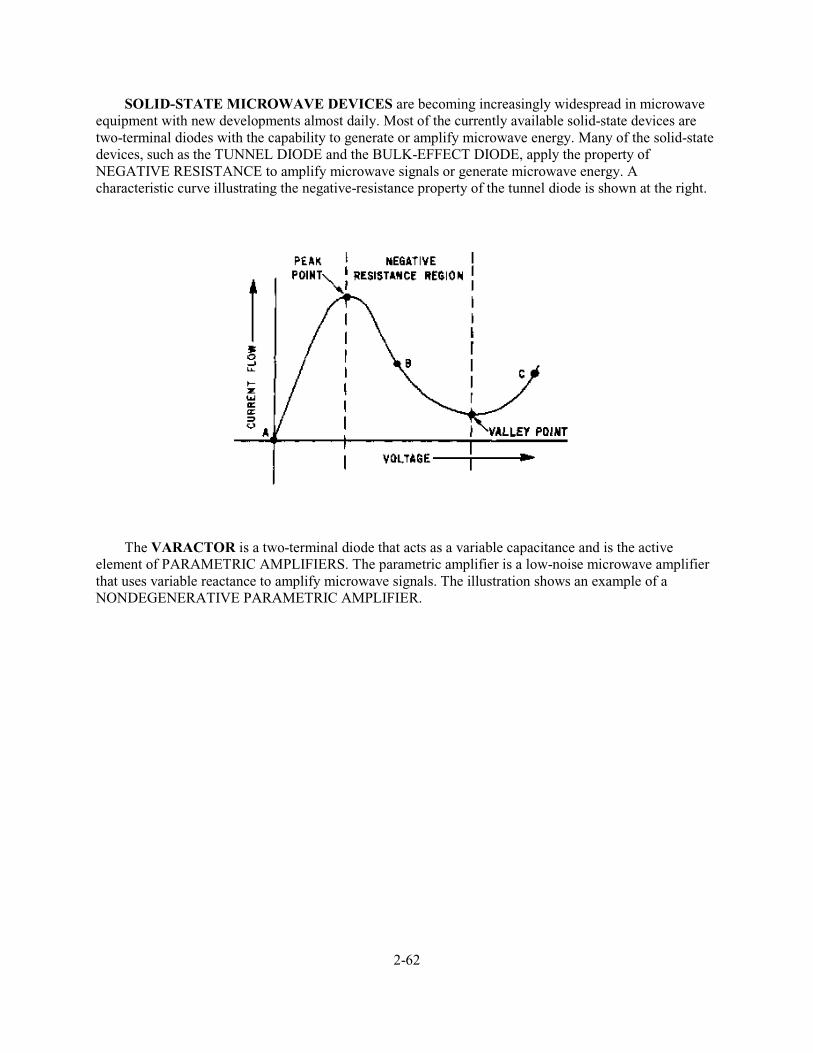
2-62
SOLID-STATE MICROWAVE DEVICES are becoming increasingly widespread in microwave equipment with new developments almost daily. Most of the currently available solid-state devices are two-terminal diodes with the capability to generate or amplify microwave energy. Many of the solid-state devices, such as the TUNNEL DIODE and the BULK-EFFECT DIODE, apply the property of NEGATIVE RESISTANCE to amplify microwave signals or generate microwave energy. A characteristic curve illustrating the negative-resistance property of the tunnel diode is shown at the right.
The VARACTOR is a two-terminal diode that acts as a variable capacitance and is the active element of PARAMETRIC AMPLIFIERS. The parametric amplifier is a low-noise microwave amplifier that uses variable reactance to amplify microwave signals. The illustration shows an example of a NONDEGENERATIVE PARAMETRIC AMPLIFIER.

2-63
ANSWERS TO QUESTIONS Q1. THROUGH Q74.
A-1. Impedance decreases.
A-2. Degenerative feedback.
A-3. Transit time causes the grid voltage and plate current to be out of phase.
A-4. Transit time.
A-5. Velocity.
A-6. The electron will be accelerated.
A-7. By alternately speeding up or slowing down the electrons.
A-8. The buncher grids.
A-9. There is no effect.
A-10. The frequency period of the buncher grid signal.
A-11. Velocity modulation.
A. CIRCUIT
AMPLIFIEDFS SIGNAL
OUTPUT
DUMMYLOAD
(UNUSEDPORT)
FERRITECIRCULATOR
FS INPUT3 GHz
FS3 GHz
FP-FS9 GHz
vv
v
vv v
SIGNALCAVITY
SIGNAL INPUT
FSINPUT
FSOUTPUT
IDLERCAVITY
VARACTORDIODEREVERSE-
BIAS BATTERY
FP PUMP 12 GHz
AMPLIFIEDFS SIGNAL
OUTPUT
DUMMYLOAD
(UNUSEDPORT)
FERRITECIRCULATOR
FS INPUT
FP-FS
vv
v
vv
v
FS
SIGNALTANK3 GHz
FP PUMP 12 GHzSIGNAL INPUT
IDLERTANK9 GHz
FS INPUTAND
OUTPUT3 GHz
VOLTAGE CONROLLEDCAPACITOR (VARACTOR)
NTS1102I-3
B. ELECTRICAL EQUIVALENT

2-64
A-12. The accelerator grid and the buncher grids.
A-13. The catcher cavity.
A-14. Amplifier.
A-15. Intermediate cavities between the input and output cavities.
A-16. A large negative pulse is applied to the cathode.
A-17. The middle cavity.
A-18. The bandwidth decreases.
A-19. Stagger tuning.
A-20. The reflector or repeller.
A-21. Velocity.
A-22. Three-quarter cycle.
A-23. Mode 2.
A-24. Power is reduced.
A-25. The half-power points of the mode.
A-26. Voltage amplification.
A-27. Used to focus the electrons into a tight beam.
A-28. The directional couplers are not physically connected to the helix.
A-29. The traveling wave must have a forward velocity equal to or less than the speed of the electrons in the beam.
A-30. The helix.
A-31. Helix.
A-32. A magnetic field.
A-33. Anode or plate.
A-34. The resonant cavities.
A-35. The permanent magnet.
A-36. The critical value of field strength.
A-37. Circular.
A-38. The negative-resistance magnetron has a split plate.
A-39. The application of the proper magnetic field.

2-65
A-40. To reduce the effects of filament bombardment.
A-41. Rising-sun block.
A-42. Series.
A-43. Working electrons.
A-44. Greater power output.
A-45. Loops and slots.
A-46. Inductive.
A-47. A cookie-cutter tuner.
A-48. Baking in.
A-49. The tunneling action.
A-50. The tuned circuit or cavity frequency.
A-51. To increase the stability.
A-52. Prevent feedback to the tuned input circuit.
A-53. Stability problems.
A-54. Variable capacitor.
A-55. Reactance.
A-56. The low-noise characteristic.
A-57. By varying the amount of capacitance in the circuit.
A-58. Supplies the electrical energy required to vary the capacitance.
A-59. Exactly double the input frequency.
A-60. The pump signal of a nondegenerative parametric amplifier is higher than twice the input signal.
A-61. Idler- or lower-sideband frequency.
A-62. The sum of the input frequency and the pump frequency.
A-63. Larger microwave power outputs.
A-64. The electrons become immobile.
A-65. Threshold.
A-66. A field of much greater intensity.
A-67. The frequency.
2-66
A-68. Pnin.
A-69. The negative-resistance property.
A-70. To form a small region of p-type material.
A-71. Lower.
A-72. Lower forward resistance and low noise.
A-73. Variable resistance.
A-74. A switching device.