negative inductance circuits for metamaterial bandwidth ... · negative inductance circuits for...
TRANSCRIPT

EPJ Appl. Metamat. 2017, 4, 11© E. Avignon-Meseldzija et al., published by EDP Sciences, 2017DOI: 10.1051/epjam/2017009
Available online at:epjam.edp-open.org
RESEARCH ARTICLE
Negative inductance circuits for metamaterial bandwidthenhancementEmilie Avignon-Meseldzija1,3, Thomas Lepetit2, Pietro Maris Ferreira1, and Fabrice Boust2,3,*
1 GeePs, UMR CNRS 8507, CentraleSupélec, Université Paris-Saclay, 91192 Gif-sur-Yvette, France2 ONERA – The French Aerospace Lab, 91120 Palaiseau, France3 SONDRA, CentraleSupélec, Université Paris-Saclay, 91192 Gif-sur-Yvette, France
* e-mail: f
This is an O
Received: 3 June 2017 / Received in final form: 19 October 2017 / Accepted: 27 October 2017
Abstract. Passive metamaterials have yet to be translated into applications on a large scale due in large part totheir limited bandwidth. To overcome this limitation many authors have suggested coupling metamaterials tonon-Foster circuits. However, up to now, the number of convincing demonstrations based on non-Fostermetamaterials has been very limited. This paper intends to clarify why progress has been so slow, i.e., thefundamental difficulty in making a truly broadband and efficient non-Foster metamaterial. To this end, weconsider two families of metamaterials, namely Artificial Magnetic Media and Artificial Magnetic Conductors.In both cases, it turns out that bandwidth enhancement requires negative inductance with almost zeroresistance. To estimate bandwidth enhancement with actual non-Foster circuits, we consider two classes of suchcircuits, namely Linvill and gyrator. The issue of stability being critical, both metamaterial families are studiedwith equivalent circuits that include advanced models of these non-Foster circuits. Conclusions are different forArtificial Magnetic Media coupled to Linvill circuits and Artificial Magnetic Conductors coupled to gyratorcircuits. In the first case, requirements for bandwidth enhancement and stability are very hard to meetsimultaneously whereas, in the second case, an adjustment of the transistor gain does significantly increasebandwidth.
Keywords: Metamaterials / Non-Foster circuit / Linvill / Gyrator / Artificial magnetic media / Artificialmagnetic conductor
1 Introduction
Ever since the turn of the millennium, metamaterials havepaved the way for very innovative and promisingpropositions. However, in most early demonstrations,the useful frequency bandwidth was quite limited andthat significantly hindered the translation of metamate-rials concepts into industrial applications. Quickly, it wasrealized that these narrow bandwidths were inherentlylinked to the linear and passive, thus causal, nature ofmetamaterials [1–3]. Following this observation, severalauthors suggested to couple metamaterials with non-Foster circuits to overcome these limitations [4–11].
Foster’s theorem states that the reactance of a passive,lossless, two-terminal network strictly increases withfrequency [12]. Any circuit that violates this rule is thusreferred to as non-Foster (NF). Usually, NF circuits aim togenerate pure negative reactances (negative capacitances,inductances, or both), i.e., with the least amount of
pen Access article distributed under the terms of the Creative Comwhich permits unrestricted use, distribution, and reproduction
resistance. On one hand, NF circuits have been successfullyused to improve impedance matching of small antennas, byintroducing a negative capacitance in the feeding network[13–20]. On the other hand, the number of NF circuits thatdemonstrated significant metamaterial bandwidth en-hancement with a negative inductance is still very limited[20,21], despite many proposals [5–8,11]. This paper thusfocuses only on negative inductance circuits among all non-Foster circuits.
This paper intends to clarify the fundamental difficultyin making a truly broadband and efficient NF metama-terial. To this end, we consider two families of metama-terials: Artificial Magnetic Media (AMM) and ArtificialMagnetic Conductors (AMC). These two families havebeen extensively studied, yet still hold a great potential forinnovative applications. In both cases, bandwidth en-hancement requires a non-Foster impedance able tocompensate the intrinsic positive inductance with as littleresistance as possible.
This paper is organized in four parts. In the first one, wepresent both AMMs and AMCs, highlighting in both casesthe need for NF circuits. In the second one, we introduce
mons Attribution License (http://creativecommons.org/licenses/by/4.0),in any medium, provided the original work is properly cited.
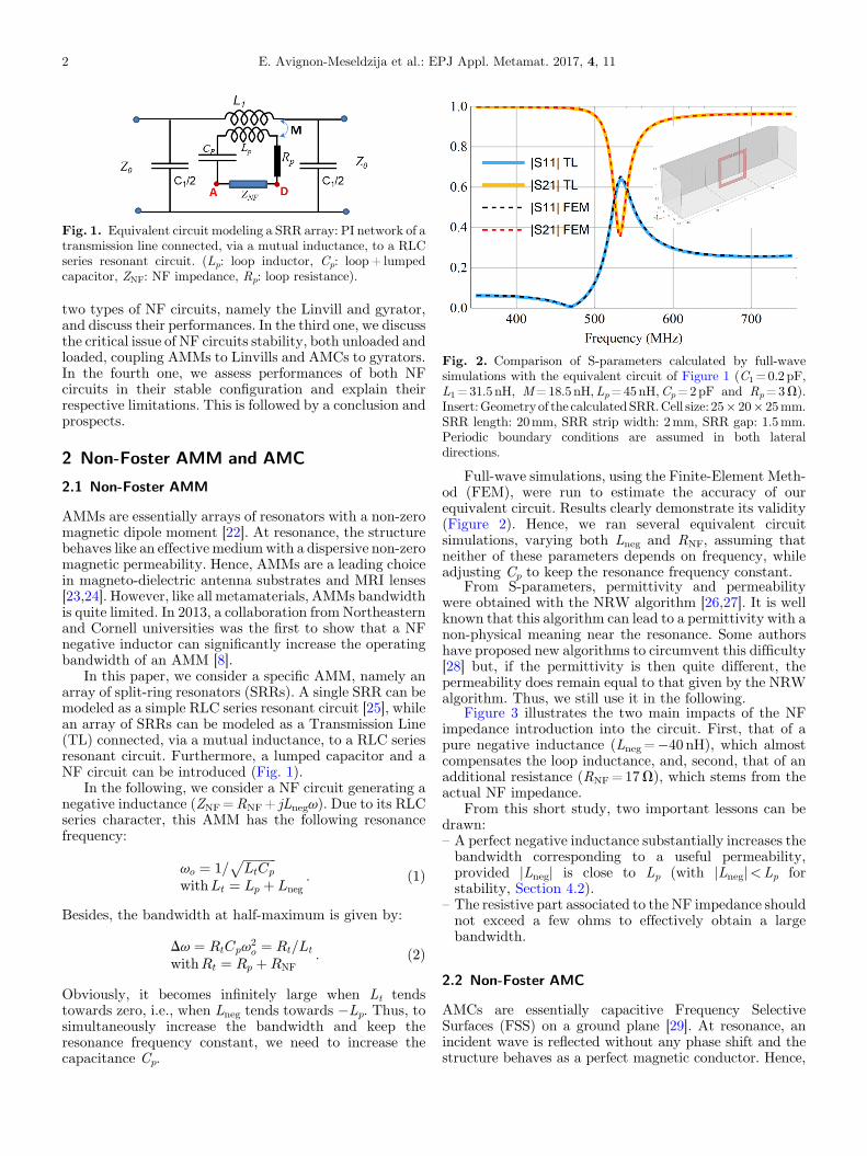
Fig. 1. Equivalent circuit modeling a SRR array: PI network of atransmission line connected, via a mutual inductance, to a RLCseries resonant circuit. (Lp: loop inductor, Cp: loop+ lumpedcapacitor, ZNF: NF impedance, Rp: loop resistance).
Fig. 2. Comparison of S-parameters calculated by full-wavesimulations with the equivalent circuit of Figure 1 (C1=0.2 pF,L1=31.5 nH, M=18.5nH,Lp=45nH,Cp=2pF and Rp=3V).Insert:Geometryof the calculatedSRR.Cell size: 25� 20� 25mm.SRR length: 20mm, SRR strip width: 2mm, SRR gap: 1.5mm.Periodic boundary conditions are assumed in both lateraldirections.
2 E. Avignon-Meseldzija et al.: EPJ Appl. Metamat. 2017, 4, 11
two types of NF circuits, namely the Linvill and gyrator,and discuss their performances. In the third one, we discussthe critical issue of NF circuits stability, both unloaded andloaded, coupling AMMs to Linvills and AMCs to gyrators.In the fourth one, we assess performances of both NFcircuits in their stable configuration and explain theirrespective limitations. This is followed by a conclusion andprospects.
2 Non-Foster AMM and AMC
2.1 Non-Foster AMM
AMMs are essentially arrays of resonators with a non-zeromagnetic dipole moment [22]. At resonance, the structurebehaves like an effectivemediumwith a dispersive non-zeromagnetic permeability. Hence, AMMs are a leading choicein magneto-dielectric antenna substrates and MRI lenses[23,24]. However, like all metamaterials, AMMs bandwidthis quite limited. In 2013, a collaboration from Northeasternand Cornell universities was the first to show that a NFnegative inductor can significantly increase the operatingbandwidth of an AMM [8].
In this paper, we consider a specific AMM, namely anarray of split-ring resonators (SRRs). A single SRR can bemodeled as a simple RLC series resonant circuit [25], whilean array of SRRs can be modeled as a Transmission Line(TL) connected, via a mutual inductance, to a RLC seriesresonant circuit. Furthermore, a lumped capacitor and aNF circuit can be introduced (Fig. 1).
In the following, we consider a NF circuit generating anegative inductance (ZNF=RNF+ jLnegv). Due to its RLCseries character, this AMM has the following resonancefrequency:
vo ¼ 1=ffiffiffiffiffiffiffiffiffiffiffiLtCp
pwithLt ¼ Lp þ Lneg
: ð1Þ
Besides, the bandwidth at half-maximum is given by:
Dv ¼ RtCpv2o ¼ Rt=Lt
withRt ¼ Rp þRNF: ð2Þ
Obviously, it becomes infinitely large when Lt tendstowards zero, i.e., when Lneg tends towards �Lp. Thus, tosimultaneously increase the bandwidth and keep theresonance frequency constant, we need to increase thecapacitance Cp.
Full-wave simulations, using the Finite-Element Meth-od (FEM), were run to estimate the accuracy of ourequivalent circuit. Results clearly demonstrate its validity(Figure 2). Hence, we ran several equivalent circuitsimulations, varying both Lneg and RNF, assuming thatneither of these parameters depends on frequency, whileadjusting Cp to keep the resonance frequency constant.
From S-parameters, permittivity and permeabilitywere obtained with the NRW algorithm [26,27]. It is wellknown that this algorithm can lead to a permittivity with anon-physical meaning near the resonance. Some authorshave proposed new algorithms to circumvent this difficulty[28] but, if the permittivity is then quite different, thepermeability does remain equal to that given by the NRWalgorithm. Thus, we still use it in the following.
Figure 3 illustrates the two main impacts of the NFimpedance introduction into the circuit. First, that of apure negative inductance (Lneg=�40 nH), which almostcompensates the loop inductance, and, second, that of anadditional resistance (RNF=17V), which stems from theactual NF impedance.
From this short study, two important lessons can bedrawn:
– A perfect negative inductance substantially increases thebandwidth corresponding to a useful permeability,provided |Lneg| is close to Lp (with |Lneg|<Lp forstability, Section 4.2).–
The resistive part associated to the NF impedance shouldnot exceed a few ohms to effectively obtain a largebandwidth.2.2 Non-Foster AMC
AMCs are essentially capacitive Frequency SelectiveSurfaces (FSS) on a ground plane [29]. At resonance, anincident wave is reflected without any phase shift and thestructure behaves as a perfect magnetic conductor. Hence,

Fig. 3. Effective permeability (real part) of a SRR array vsfrequency: (1) Lneg= 0,Cp=2pF, RNF=0V (2) Lneg=�40 nH,Cp=18 pF,RNF=0V (3) Lneg=�40 nH,Cp=18 pF,RNF=17V.
Fig. 4. Equivalent circuit modeling a patch array: short-circuited transmission line connected to a capacitance, thusforming a LC series resonant circuit. (Ld: short-circuit inductor,Cg: patch+ lumped capacitor, ZNF: NF impedance).
Fig. 5. Phase on reflection of a patch array vs frequency: (1) Nonegative inductance,Cg=Cgl = 12.8 pF (2) Lneg=�32.2 nH,Cg=Cg0= 0.25 pF, RNF 0V (3) Lneg=�32.2 nH,Cg=Cg0= 0.25 pF,RNF=3V (4) Lneg=�32.2 nH,Cg=Cg0= 0.25 pF, RNF=10V.
Fig. 6. Small signal model of the MOSFET [37]. The three nodescorrespond to the Gate (G), Source (S), and Drain (D).
E. Avignon-Meseldzija et al.: EPJ Appl. Metamat. 2017, 4, 11 3
AMCs are a leading choice for low-profile antennas or thinradar-absorbing materials [30–32]. AMCs are especiallyattractiveat lowoperating frequencies due to their extremelysmall thickness. However, like all metamaterials, AMCsbandwidth is quite limited. In 2011, a group from HRLLaboratories was the first to show that a NF negativeinductor can significantly increase the operating bandwidthof an AMC [21].
In this paper, we consider a specific AMC, namely apatch array placed at a distance d above a ground plane.When d is small compared to l, the propagation betweenthe FSS and the ground plane is equivalent to aninductance Ld=m0d. Thus, an AMC is equivalent to aLC parallel resonant circuit (Fig. 4).
In the following, we consider a NF circuit generating anegative inductance (ZNF=RNF+ jLnegv). Due to its LCparallel character, this AMC has the following resonancefrequency:
vo ¼ 1=ffiffiffiffiffiffiffiffiffiffiffiLtCg
pwithLt ¼ 1
Lpþ 1
Lneg
� ��1 : ð3Þ
Besides, the derivative of the phase shift on resonance,which is the relevant figure of merit, is given by:
df
dv
� �v0
¼ �4Z0Cg ¼ �4Z0=ðv20LtÞ: ð4Þ
Obviously, it becomes infinitely small when Lt tendstowards infinity, i.e., when Lneg tends towards �Ld. Thus,unlike the AMM, to simultaneously increase the bandwidthand keep the resonance frequency constant, we need todecrease the capacitance Cg.
As for the AMM, full-wave simulations were run toestimate the accuracy of our equivalent circuit. Resultsclearly demonstrate its validity (not shown). Hence, we ranseveral equivalent circuit simulations, varying both Lnegand RNF, assuming that neither of these parametersdepends on frequency, while adjusting Cg to keep theresonance frequency constant.
We have considered a patch array placed at d=25mmover a ground plane (Ld=31.4 nH), with a small patchcapacitance (0.25 pF). With these parameters, the struc-ture behaves as an AMC around 1.6GHz. Since our initialworking frequency is too high, we have two options to lowerit down to 250 MHz.We can either add a lumped capacitorto increase Cg (up to 12.8 pF) or add a negative inductor toincrease Lt (up to 1290 nH for Lneg=�32.2 nH).
Figure 5 illustrates the two main impacts of the NFimpedance introduction into the circuit. First, that of apure negative inductance (Lneg=�32.2 nH), which almostcompensates the loop inductance, and, second, that of anadditional resistance (RNF=3 or 10V), which stems fromthe actual NF impedance.
From this short study, two important lessons can bedrawn:
– A perfect negative inductance substantially increases thebandwidth corresponding to a PMC behavior, provided|Lneg| is close to Ld (with |Lneg|>Ld for stability,Section 4.4).
a)
4 E. Avignon-Meseldzija et al.: EPJ Appl. Metamat. 2017, 4, 11
–
b)
Fig. 7. a) Linvill circuit with MOSFET transistors. b) Small-signal model of the Linvill circuit.
The resistive part associated to the NF impedance shouldnot exceed a few ohms to effectively obtain a largebandwidth.
In summary, both AMMs and AMCs require a negativeinductance with a small resistive part. Hence, some of therequirements placed on NF circuits are common to thesetwo structures. However, onemajor difference is their seriesversus parallel character. This has dramatic consequenceson the choice of a relevant NF architecture as discussednext.
3 Negative inductance circuits
Among all possible circuit architectures that can generatenegative inductances, two have been selected: Linvill (aNegative Impedance Converter or NIC: Z!�Z) andgyrator (a Negative Impedance Inverter or NII: Z!� 1/Z). A majority of architectures proposed in the literatureare based on these two.
Many authors pointed out the negative impact oftransmission lines and transistor packages on Non-Fostercircuits [33–36]. As Loncar et al. have shown, transmissionlines have an impact on both reactance and resistance.Thus, the electrical length of transmission lines should bereduced as much as possible. Consequently, we havedecided to work with integrated circuits.
We chose to base both topologies on MOSFET (MetalOxide Semiconductor Field Effect Transistor), which is themost commonly used transistor in microelectronics. Theclassical small signal model of the MOSFET, presented inFigure 6, is used in the following [37].
In Figure 6, gm is the transistor transconductance, vgsits gate-source voltage, r0 its output resistance (with orwithout a drain resistor in parallel), and Cgs, Cgd, Cds itsparasitic capacitances. Values of the above parametersdepend on technology, bias point, and transistor dimen-sions. For instance, larger transistors have larger parasiticcapacitances. We chose to consider a mature and readilyaccessible technology (CMOS 0.35mm). Following valuesremain constant throughout the paper: Cpar=Cgs+Cds=0.4 pF,Cgd= 0.2 pF, r0= 2 kV.
3.1 Negative inductance based on Linvill circuits
The principle of the Linvill circuit was first published in[38]. Since then, a large number of implementations havebeen proposed, some using discrete components [15,39–41],and others fully integrated [42,43]. Since it is a NIC, itprovides negative inductance/capacitance when loadedwith an inductor/capacitor.
Figure 7a presents the principle of the Linvill circuitwhile Figure 7b presents its small-signal model. Consider-ing a simplified model, without parasitic capacitors, theinput impedance is given by:
ZLinv ¼ 2r0gmr0 þ 1
� ZLgmr0 � 1
gmr0 þ 1≈
2
gm� ZL: ð5Þ
The final approximation was obtained by assuminggmr0>> 1. Thus, for the Linvill, the reactive part of theimpedance only depends on the load and the resistive partis positive and decreases with gm.
At first glance, it would then seem as though one onlyneed consider a pure inductance (ZL= jLv) together with alarge gm. However, a large gm implies large powerconsumption, as shown in [42] where gm has the unusuallylarge value of 30mS. A practical alternative is to add acompensation resistor in series (ZL=R+ jLv) to decreasethe resistive part. In the following, we consider the fullmodel, i.e., including compensation resistor, parasiticcapacitors and without any approximation (for thecomplete expression of the input impedance see AppendixA.1).
In the Linvill circuit, two parameters are readilycontrollable: gm and R. Even within the full model, theyafford enough degrees of freedom to cancel the real part ofthe NF impedance at any frequency of interest. Toillustrate this fact, we consider a specific example (gm islimited to 20mS in order to consider achievable values).Figure 8 presents results that were obtained withR varyingfrom 0V to 100V (gm=20mS, L=40nH). We see that thereal part always cancels at some frequency (fRe0), whichincreases with R. Besides, we observe that the real partquickly takes on large negative values beyond fRe0.
Conclusions of this sectionare threefold.First, a negativeinductance canbeobtainedby introducingan inductor in theload impedance. Second, cancellation of the real part can beachieved either by a large gm or by adding a resistorR to theload impedance, and this canbe achieved at any frequency ofinterest. Finally, minimization of the real part on a largebandwidthcannotbedonearoundany frequencybut, rather,is achievable only at low frequencies (f< 200MHz) and forlarge compensation resistor (R> 100V).

Fig. 8. Input impedance of the Linvill circuit, ZLinv=Re(ZLinv)+ jLLinvv, assuming gm=20mS, L=40 nH and: (1)R=0V, fRe0= 900MHz (2) R=50V, fRe0= 570MHz; (3)R=100V, fRe0= 120MHz.
a)
b)
Fig. 9. a) Gyrator circuit with MOSFET transistors. b) Small-signal model of the gyrator circuit.
E. Avignon-Meseldzija et al.: EPJ Appl. Metamat. 2017, 4, 11 5
3.2 Negative inductance based on Gyrator circuits
Gyrator circuits [44,45] have been massively employed forIC implementation of active inductors to avoid integrationof passive spiral inductors [46], which take up a lot of space.Recently, this topology has even been used in an IC toobtain a negative inductance dedicated toAMCs [47]. Sinceit is a NII (Negative Impedance Inverter), it providesnegative inductance /capacitance when it is loaded with acapacitor/inductor.
Figure 9a presents the principle of the gyrator circuitwhile Figure 9b presents its small-signal model. Eachtransistor in this simplified view is actually an OperationalTransconductance Amplifier (OTA). We note that it ishighly recommended to use one-stage OTAs as multiple-stages OTAs introduce more nodes thus leading to greaterrisks of instability (for possible topologies of one-stageOTA circuits see Appendix B). In contrast to positiveactive inductors, which use two OTAs with gm of differentsigns, negative inductors use two OTA with gm of the samesign.
Considering a simplified model, without parasiticcapacitors, the input impedance is given by:
Zgyr ¼ r0ðr0 þ ZLÞr0 � ZLðg2mr20 � 1Þ ≈
1
g2m� 1
r0� 1
ZL
� �:
The final approximation was obtained by assuming bothg2mr
20≫1 and jg2mr0ZLj≫1. Thus, for the gyrator, both
reactive and resistive parts of the impedance are negativeand decrease with g2m.
At first glance, it would then seem as though one onlyneed consider a pure capacitance (ZL=1/jCv) togetherwith a large gm. However, when one goes beyond thesimplified model, resistive and reactive parts can no longerbe dissociated. In the following, we consider the fullmodel,i.e., including parasitic capacitors and without anyapproximation (for the complete expression of the inputimpedance see Appendix A.2).
In the gyrator circuit, three parameters are readilycontrollable: r0, gm and C via varactors (r0 has been keptconstant at 2 kV for simplicity). Even within the fullmodel,they afford enough degrees of freedom to cancel the real partof theNF impedance at any frequencyof interest. In contrastto the Linvill though, a thorough knowledge of parasiticcapacitances is required to achieve such cancellation. Toillustrate this fact, we consider a specific example. Figure 10presents results that were obtained for three differentcombinations of gm andC.All combinations ensure that thenegative inductanceequals�32.2 nHat250MHzbut therealpart cancels at different frequencies (fRe0). We see thatoptimal values of gm and C do not follow any simple law.
Conclusions of this section are threefold. First, anegative inductance can be obtained by introducing acapacitor in the load impedance. Second, cancellation ofthe real part can be achieved by a suitable combination ofgm andC. Finally, the real part is overall much smaller thanfor the Linvill and, thus, the exact frequency at which itdoes cancel is not as critical as its minimization to achieve alarge bandwidth.
3.3 Linvill vs. Gyrator
Both topologies can lead to the desired values of negativeinductance, but do not present the same advantages.
Concerning the quality factor Q= Im(ZNF)/Re(ZNF),Linvill circuits presents a real part that is relatively largecompared to gyrators, hence a much lower quality factor.However, it is easier to cancel the real part around thefrequency of interest with Linvills than with gyrators,thanks to the compensation resistor R. Still, it does notactually affect performances of gyrator circuits as they donot present a steep variation of the real part withfrequency. Concerning the chip area, Linvill circuits areclearly worse than gyrators as they require an inductance.Gyrator circuits are more compact and, additionally, offerthe possibility to tune gm via the bias current to change thevalue of the negative inductance. Concerning stability, it
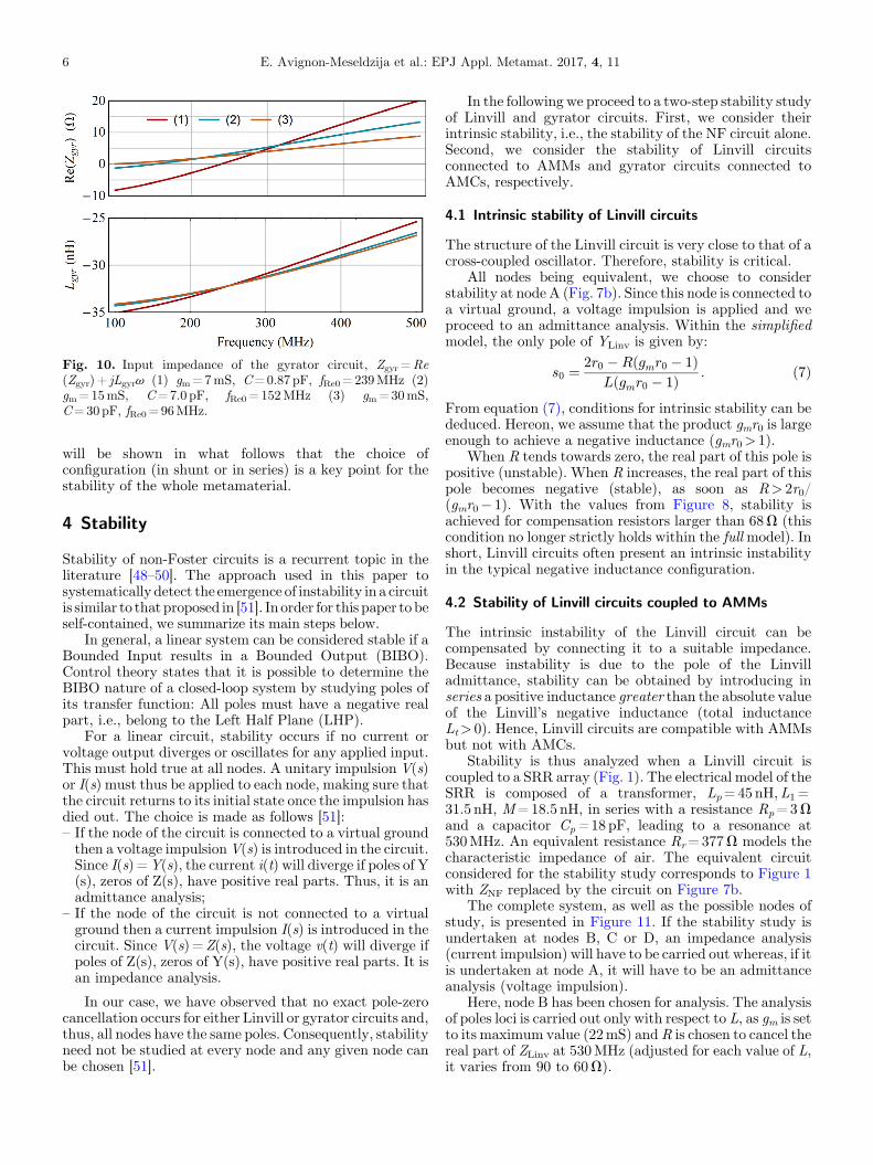
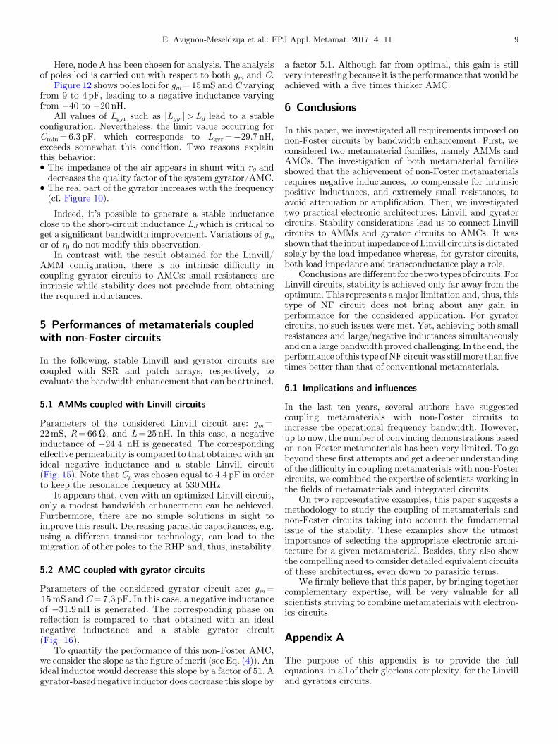
Fig. 10. Input impedance of the gyrator circuit, Zgyr =Re(Zgyr)+ jLgyrv (1) gm=7mS, C=0.87 pF, fRe0= 239MHz (2)gm=15mS, C=7.0 pF, fRe0= 152MHz (3) gm=30mS,C=30pF, fRe0= 96MHz.
6 E. Avignon-Meseldzija et al.: EPJ Appl. Metamat. 2017, 4, 11
will be shown in what follows that the choice ofconfiguration (in shunt or in series) is a key point for thestability of the whole metamaterial.
4 Stability
Stability of non-Foster circuits is a recurrent topic in theliterature [48–50]. The approach used in this paper tosystematically detect the emergence of instability in a circuitis similar to that proposed in [51]. In order for this paper to beself-contained, we summarize its main steps below.
In general, a linear system can be considered stable if aBounded Input results in a Bounded Output (BIBO).Control theory states that it is possible to determine theBIBO nature of a closed-loop system by studying poles ofits transfer function: All poles must have a negative realpart, i.e., belong to the Left Half Plane (LHP).
For a linear circuit, stability occurs if no current orvoltage output diverges or oscillates for any applied input.This must hold true at all nodes. A unitary impulsion V(s)or I(s) must thus be applied to each node, making sure thatthe circuit returns to its initial state once the impulsion hasdied out. The choice is made as follows [51]:
– If the node of the circuit is connected to a virtual groundthen a voltage impulsionV(s) is introduced in the circuit.Since I(s)=Y(s), the current i(t) will diverge if poles of Y(s), zeros of Z(s), have positive real parts. Thus, it is anadmittance analysis;–
If the node of the circuit is not connected to a virtualground then a current impulsion I(s) is introduced in thecircuit. Since V(s)=Z(s), the voltage v(t) will diverge ifpoles of Z(s), zeros of Y(s), have positive real parts. It isan impedance analysis.In our case, we have observed that no exact pole-zerocancellation occurs for either Linvill or gyrator circuits and,thus, all nodes have the same poles. Consequently, stabilityneed not be studied at every node and any given node canbe chosen [51].
In the following we proceed to a two-step stability studyof Linvill and gyrator circuits. First, we consider theirintrinsic stability, i.e., the stability of the NF circuit alone.Second, we consider the stability of Linvill circuitsconnected to AMMs and gyrator circuits connected toAMCs, respectively.
4.1 Intrinsic stability of Linvill circuits
The structure of the Linvill circuit is very close to that of across-coupled oscillator. Therefore, stability is critical.
All nodes being equivalent, we choose to considerstability at node A (Fig. 7b). Since this node is connected toa virtual ground, a voltage impulsion is applied and weproceed to an admittance analysis. Within the simplifiedmodel, the only pole of YLinv is given by:
s0 ¼ 2r0 �Rðgmr0 � 1ÞLðgmr0 � 1Þ : ð7Þ
From equation (7), conditions for intrinsic stability can bededuced. Hereon, we assume that the product gmr0 is largeenough to achieve a negative inductance (gmr0> 1).
When R tends towards zero, the real part of this pole ispositive (unstable). When R increases, the real part of thispole becomes negative (stable), as soon as R> 2r0/(gmr0� 1). With the values from Figure 8, stability isachieved for compensation resistors larger than 68V (thiscondition no longer strictly holds within the fullmodel). Inshort, Linvill circuits often present an intrinsic instabilityin the typical negative inductance configuration.
4.2 Stability of Linvill circuits coupled to AMMs
The intrinsic instability of the Linvill circuit can becompensated by connecting it to a suitable impedance.Because instability is due to the pole of the Linvilladmittance, stability can be obtained by introducing inseries a positive inductance greater than the absolute valueof the Linvill’s negative inductance (total inductanceLt> 0). Hence, Linvill circuits are compatible with AMMsbut not with AMCs.
Stability is thus analyzed when a Linvill circuit iscoupled to a SRR array (Fig. 1). The electrical model of theSRR is composed of a transformer, Lp=45nH,L1=31.5 nH, M=18.5 nH, in series with a resistance Rp=3Vand a capacitor Cp= 18 pF, leading to a resonance at530MHz. An equivalent resistance Rr=377V models thecharacteristic impedance of air. The equivalent circuitconsidered for the stability study corresponds to Figure 1with ZNF replaced by the circuit on Figure 7b.
The complete system, as well as the possible nodes ofstudy, is presented in Figure 11. If the stability study isundertaken at nodes B, C or D, an impedance analysis(current impulsion) will have to be carried out whereas, if itis undertaken at node A, it will have to be an admittanceanalysis (voltage impulsion).
Here, node B has been chosen for analysis. The analysisof poles loci is carried out only with respect to L, as gm is setto its maximum value (22mS) andR is chosen to cancel thereal part of ZLinv at 530MHz (adjusted for each value of L,it varies from 90 to 60V).

Fig. 11. Equivalent circuit of the Linvill NIC coupled to the SRR array (AMM). All four nodes and their respective impedance/admittance analysis are represented.
Fig. 12. Poles loci at nodeB. gm is constant (22mS).To cancel thereal part of ZLinv at 530MHz,R varies from 90 to 60Vwhen L goesfrom 5 to 30nH. The inset shows the evolution of Lmax with gm.
E. Avignon-Meseldzija et al.: EPJ Appl. Metamat. 2017, 4, 11 7
Figure 12 shows poles loci obtained for L varyingbetween 5 and 30 nH, leading to a negative inductancevarying from�2 to�30 nH. It can be seen that a value of Lgreater than Lmax=26 nH, which corresponds to LLinv=�28.2 nH at 530MHz, places two poles in the Right HalfPlane (RHP). Since a total inductance close to zero(Lp=45nH) is critical to get a significant bandwidthimprovement, subpar performances can be anticipated.The inset presents the evolution of Lmax with gm: increasinggm further leads to a slowly decreasing Lmax.
There is an inherent difficulty in coupling Linvillcircuits to AMMs: to obtain small resistances a large gm isneeded but with a large gm the possible negativeinductances are limited by stability considerations.
4.3 Intrinsic stability of gyrator circuits
All nodes being equivalent, we choose to consider stabilityat node A (Fig. 9b). Since this node is not connected to avirtual ground, a current impulsion is applied and weproceed to an impedance analysis. Within the simplifiedmodel, the only pole of Zgyr is given by:
s0 ¼ g2mr20 � 1
r0C: ð8Þ
From equation (8), conditions for intrinsic stabilitycan be straightforwardly deduced. When gm> 1/r0, thereal part of this pole is positive (unstable) and theimpedance is mostly inductive. When gm< 1/r0, the realpart of this pole is negative (stable) and the impedance ismostly resistive.
It means that as long as the impedance is mostlyinductive the negative inductance created by the gyratorcircuit is intrinsically instable.
4.4 Stability of gyrator circuits coupled to AMCs
The intrinsic instability of the gyrator circuit can becompensated by connecting it to a suitable impedance.
Because instability is due to the pole of the gyratorimpedance, stability can never be restored by connecting apositive inductor in series [50]. However, a stableconfiguration can be obtained in shunt with a positiveinductance smaller than the absolute value of the gyrator’snegative inductance (total inductance Lt> 0)[50]. Hence,gyrator circuits are compatible with AMCs but not withAMMs.
Stability is thus analyzed when a gyrator circuit iscoupled to a patch array (Fig. 4). The electrical model ofthe patch array is composed of a capacitor (Cg0= 0.25 pF)

Fig. 13. Equivalent circuit of the gyrator NII coupled to the patch array (AMC). All three nodes and their respective impedance/admittance analysis are represented.
Fig. 14. Poles loci at node A (gm=15mS,C varies from 9pF to 4 pF when Lgyr goes from �40 nH to �20 nH).
Fig. 15. Effective permeability of a SRR array vs. frequency forthe following three configurations: (1) Initial SRR array,Cp=2pF (2) Ideal negative inductance, Cp=18pF,Lneg=�40 nH, RNF=0V (3) Stable Linvill circuit Cp=4,4 pF,Lneg=�24.4 nH, RNF=66V.
Fig. 16. Phase on reflection of a patch array vs. frequency for thefollowing three configurations: (1) Initial patch array, Cg=Cgl =12.8 pF (2) Ideal negative inductance, Cg=Cg0= 0.25 pF,Lneg=�32.2 nH, RNF=0V (3) Stable gyrator circuit, Cg0= 0.25 pF,Lneg=�31.9 nH, RNF=3.2V.
8 E. Avignon-Meseldzija et al.: EPJ Appl. Metamat. 2017, 4, 11
in shunt with an inductor Ld=31.4 nH. An equivalentresistance Rr=377V models the impedance of air. Theequivalent circuit considered for the stability studycorresponds to Figure 1 with ZNF replaced by the circuiton Figure 9b.
The complete system, as well as the possible nodes ofstudy, is presented in Figure 11. If the stability study isundertaken at nodes A or C, an impedance analysis(current impulsion) will have to be carried out whereas, if itis undertaken at node B, it will have to be an admittanceanalysis (voltage impulsion).
E. Avignon-Meseldzija et al.: EPJ Appl. Metamat. 2017, 4, 11 9
Here, node A has been chosen for analysis. The analysisof poles loci is carried out with respect to both gm and C.
Figure 12 shows poles loci for gm=15mS and C varyingfrom 9 to 4 pF, leading to a negative inductance varyingfrom �40 to �20 nH.
All values of Lgyr such as |Lgyr|>Ld lead to a stableconfiguration. Nevertheless, the limit value occurring forCmin= 6.3 pF, which corresponds to Lgyr=�29.7 nH,exceeds somewhat this condition. Two reasons explainthis behavior:
* The impedance of the air appears in shunt with r0 anddecreases the quality factor of the system gyrator/AMC.*
The real part of the gyrator increases with the frequency(cf. Figure 10).Indeed, it’s possible to generate a stable inductanceclose to the short-circuit inductance Ld which is critical toget a significant bandwidth improvement. Variations of gmor of r0 do not modify this observation.
In contrast with the result obtained for the Linvill/AMM configuration, there is no intrinsic difficulty incoupling gyrator circuits to AMCs: small resistances areintrinsic while stability does not preclude from obtainingthe required inductances.
5 Performances of metamaterials coupledwith non-Foster circuits
In the following, stable Linvill and gyrator circuits arecoupled with SSR and patch arrays, respectively, toevaluate the bandwidth enhancement that can be attained.
5.1 AMMs coupled with Linvill circuits
Parameters of the considered Linvill circuit are: gm=22mS, R=66V, and L=25nH. In this case, a negativeinductance of �24.4 nH is generated. The correspondingeffective permeability is compared to that obtained with anideal negative inductance and a stable Linvill circuit(Fig. 15). Note that Cp was chosen equal to 4.4 pF in orderto keep the resonance frequency at 530MHz.
It appears that, even with an optimized Linvill circuit,only a modest bandwidth enhancement can be achieved.Furthermore, there are no simple solutions in sight toimprove this result. Decreasing parasitic capacitances, e.g.using a different transistor technology, can lead to themigration of other poles to the RHP and, thus, instability.
5.2 AMC coupled with gyrator circuits
Parameters of the considered gyrator circuit are: gm=15mS and C=7,3 pF. In this case, a negative inductanceof �31.9 nH is generated. The corresponding phase onreflection is compared to that obtained with an idealnegative inductance and a stable gyrator circuit(Fig. 16).
To quantify the performance of this non-Foster AMC,we consider the slope as the figure of merit (see Eq. (4)). Anideal inductor would decrease this slope by a factor of 51. Agyrator-based negative inductor does decrease this slope by
a factor 5.1. Although far from optimal, this gain is stillvery interesting because it is the performance that would beachieved with a five times thicker AMC.
6 Conclusions
In this paper, we investigated all requirements imposed onnon-Foster circuits by bandwidth enhancement. First, weconsidered two metamaterial families, namely AMMs andAMCs. The investigation of both metamaterial familiesshowed that the achievement of non-Foster metamaterialsrequires negative inductances, to compensate for intrinsicpositive inductances, and extremely small resistances, toavoid attenuation or amplification. Then, we investigatedtwo practical electronic architectures: Linvill and gyratorcircuits. Stability considerations lead us to connect Linvillcircuits to AMMs and gyrator circuits to AMCs. It wasshown that the input impedance ofLinvill circuits is dictatedsolely by the load impedance whereas, for gyrator circuits,both load impedance and transconductance play a role.
Conclusions aredifferent for thetwotypesof circuits.ForLinvill circuits, stability is achieved only far away from theoptimum. This represents a major limitation and, thus, thistype of NF circuit does not bring about any gain inperformance for the considered application. For gyratorcircuits, no such issues were met. Yet, achieving both smallresistances and large/negative inductances simultaneouslyand on a large bandwidth proved challenging. In the end, theperformance of this type ofNFcircuitwas stillmore thanfivetimes better than that of conventional metamaterials.
6.1 Implications and influences
In the last ten years, several authors have suggestedcoupling metamaterials with non-Foster circuits toincrease the operational frequency bandwidth. However,up to now, the number of convincing demonstrations basedon non-Foster metamaterials has been very limited. To gobeyond these first attempts and get a deeper understandingof the difficulty in coupling metamaterials with non-Fostercircuits, we combined the expertise of scientists working inthe fields of metamaterials and integrated circuits.
On two representative examples, this paper suggests amethodology to study the coupling of metamaterials andnon-Foster circuits taking into account the fundamentalissue of the stability. These examples show the utmostimportance of selecting the appropriate electronic archi-tecture for a given metamaterial. Besides, they also showthe compelling need to consider detailed equivalent circuitsof these architectures, even down to parasitic terms.
We firmly believe that this paper, by bringing togethercomplementary expertise, will be very valuable for allscientists striving to combine metamaterials with electron-ics circuits.
Appendix A
The purpose of this appendix is to provide the fullequations, in all of their glorious complexity, for the Linvilland gyrators circuits.

Fig. A.1. Comparison of the simplified and full model of the Linvill circuit from 100 to 900MHz. Circuit parameters are gm=20mS,R=100V, and L=40 nH. (Top) Real part of the input impedance. (Bottom) Equivalent inductance of the input impedance.
10 E. Avignon-Meseldzija et al.: EPJ Appl. Metamat. 2017, 4, 11
A.1 Linvill
The input impedance of the full model, with compensationresistor, parasitic capacitors and no approximation is givenby:
See Eq. (A.1) at the bottomSimplified and full models are compared on Figure A.1
for a specific case (gm=20mS, R=100V, L=40nH, sameparameters as Figure 8). All other parameters are given inSection 3.
As can be seen from Figure A.1, there is little to noimpact of the approximation on the simplifiedmodel exceptfor a small upwards shift of the inductance. However, onlythe full model should be used at frequencies above 500MHzsince resistive parts of the input impedance for simplifiedand full models strongly deviate from each otherafterwards.
ZLinv ¼ 2r0 þ Rð1gmr0Þ þ j!Rr0ð4C gd þ C
ðgmr0 þ 1þ j!C parr0Þð
Zgyr ¼ r0ð1þ j!r0ð41g2mr
2o þ j!r0ð4C gdð1þ gmr0Þ þ CL þ C
withCL ¼ Cpar þ C
A.2 Gyrator
The input impedance of the full model, with compensationresistor, parasitic capacitors and no approximation is givenby:
See Eq. (A.2.1) at the bottomSimplified and full models are compared on
Figure A.2 for a specific case (gm=15mS, C=7 pF,same parameters as Figure 10). All other parameters aregiven in Section 3.
As can be seen from Figure A.2, there is a small butsignificant impact of the approximation on the simplifiedmodel as it predicts only positive resistance, therebymissing potential instabilities. However, unlike theLinvill, the simplified model of the gyrator is valid on avery wide frequency range since the overall deviation ismuch smaller.
parÞj!Lðgmr01ÞLr0ðC par þ 4C gdÞ!2
1þ j2RC gd!2LC gd!2Þ : ðA:1Þ
C gd þ CLÞparÞ!2r2oð2C gdðCL þ C parÞ þ CLCparÞ : ðA:2:1Þ

Fig. A.2. Comparison of the simplified and full model of the gyrator circuit from 100 to 500MHz. Circuit parameters are gm=15mS,and C=7pF. (Top) Real part of the input impedance. (Bottom) Equivalent inductance of the input impedance.
RL
M1vin
iout
Cgd
Cgs Cdsgmvgs rout1
vin
iout
RL
Cgd
Cgs Coutgmvgs
vin
iout
r0
M1vin
iout
Vbias M2
a)
b)
Fig. B.1. Single Input Single Output (SISO) configurations of OTA.
E. Avignon-Meseldzija et al.: EPJ Appl. Metamat. 2017, 4, 11 11

ZL
VDDAc ve Load
Cross-CoupledTransistors
Current source
IN+ IN-
ZL
VDDPassive Load
Cross-CoupledTransistorsIN+ IN-
Itune
Tunable current source
a) b)
Fig. B.2. Linvill circuit: a) published in [42], b) published in [39].
12 E. Avignon-Meseldzija et al.: EPJ Appl. Metamat. 2017, 4, 11
Appendix B
The purpose of this appendix is to provide to the reader asynthetic overview on possible circuits for the gyrator andthe Linvill topologies. It could not be an exhaustivepresentation.
B.1 Gyrator
The gyrator topology is based on two OTA (OperationalTransconductance Amplifier). In the case of Non Foster,due to the high risk of instability it is better to limit thenumber of nodes and then the number of stages in theOTA. Two basic configurations are presented inFigure B.1. The equivalent small signal model is coherentwith the small signal model of a MOSFET transistor. Itmeans that the studies presented in this article are valid forthese configurations, by only modifying the values ofparameters of the small signal model, particularly r0. Anexample of gyrator based on two one stage inverter basedOTA is proposed in [52]
B.2 Linvill
The Linvill circuit has been achieved many times withvarying technologies (bipolar transistors or MOSFET,integrated or with lumped elements). We propose inFigure B.2 twoMOSFET-based recently published circuits[42,39]. As it can be seen on the figure, the drains of thecross-coupled transistors could be connected to transistorsor resistors. So in the small signal model of the MOSFET itwill change the order of magnitude of r0.
References
1. D. Youla, L. Castriota, H. Carlin, IRE Trans. Circ. Theor. 6,102 (1959)
2. S.A. Tretyakov, Microw. Opt. Technol. Lett. 31, 163 (2001)
3. S.A. Tretyakov, S.I. Maslovski, IEEE Antennas Propag.Mag. 49, 37 (2007)
4. S. Hrabar et al., Appl. Phys. Lett. 99, 254103 (2011)5. S. Hrabar, I. Krois, A. Kiricenko, Metamaterials 4, 89 (2010)6. P.-Y. Chen, C. Argyropoulos, A. Alù, Phys. Rev. Lett. 111,
233001 (2013)7. D.F. Sievenpiper, IEEE Antennas Wirel. Propag. Lett. 10,
231 (2011)8. S. Saadat et al., IEEE Trans. Antennas Propag. 61, 1210
(2013)9. F. Gao et al., Electron. Lett. 50, 1616 (2014)10. Y. Ding, V. Fusco, Microw. Opt. Technol. Lett. 54, 2111
(2012)11. M. Barbuto et al., IEEE Trans. Antennas Propag. 61, 1219
(2013)12. C.G. Montgomery, R.H. Dicke, E.M. Purcell, Principles of
microwave circuits (Iet, 1948)13. A.D. Harris, G.A. Myers, DTIC Document, 196814. J.T. Aberle, R. Loepsinger-Romak, Synth. Lect. Antennas 2,
1 (2007)15. S.E. Sussman-Fort, R.M. Rudish, IEEE Trans. Antennas
Propag. 57, 2230 (2009)16. C.R. White, J.S. Colburn, R.G. Nagele, IEEE Antennas
Wirel. Propag. Lett. 11, 584 (2012)17. O.O. Tade, P. Gardner, P.S. Hall, in: 42nd European
Microwave Conference (EuMC), 2012, p. 61318. S.D. Stearns, in: IEEE International Symposium on Anten-
nas and Propagation (APSURSI), 2011, p. 194219. M.M. Jacob, J. Long, D.F. Sievenpiper, in Antennas and
Propagation Society International Symposium (APSURSI),IEEE., 2012, p. 1
20. N. Zhu, R.W. Ziolkowski, Appl. Phys. Lett. 101, 024107(2012)
21. D.J. Gregoire, C.R. White, J.S. Colburn, IEEE AntennasWirel. Propag. Lett. 10, 1586 (2011)
22. S.A. Tretyakov, Analytical modeling in applied electro-magnetics (Artech House, 2003)
23. R.C. Hansen, M. Burke, Microw. Opt. Technol. Lett. 26, 75(2000)
24. M.J. Freire, R. Marques, L. Jelinek, Appl. Phys. Lett. 93,231108 (2008)

E. Avignon-Meseldzija et al.: EPJ Appl. Metamat. 2017, 4, 11 13
25. H. Mosallaei, K. Sarabandi, IEEE Antennas Wirel. Propag.Lett. 4, 5 (2005)
26. A.M. Nicolson, G.F. Ross, IEEE Trans. Instrum. Meas. 19,377 (1970)
27. W.B. Weir, Proc. IEEE 62, 33 (1974)28. C.R. Simovski, Opt. Spectrosc. 107, 726 (2009)29. B.A. Munk, Frequency Selective Surfaces: theory and design
(John Wiley and Sons, 2005)30. S.R. Best, D.L. Hanna, IEEE Antennas Propag. Mag. 50, 52
(2008)31. Y. Fan, Y. Rahmat-Samii, IEEE Trans. Antennas Propag.
51, 2691 (2003)32. N. Engheta, in Antennas and Propagation Society Interna-
tional Symposium, 2002 (IEEE, 2002), p. 39233. J. Lončar, D. Muha, S. Hrabar, in 2013: IEEE International
Symposium on Antennas and Propagation & USNC/URSINational Radio Science Meeting 2015, p. 73
34. T. Kaneko, Y. Horii, in: 2013 Asia-Pacific MicrowaveConference Proceedings (APMC), 2013, p. 1194
35. A.M. Elfrgani, R.G. Rojas, in: IEEE MTT-S InternationalMicrowave Symposium, 2015, p. 1
36. J. Loncar, S. Hrabar, D. Muha, IEEE Trans. AntennasPropag. 65, 390 (2017)
37. R.J. Baker, CMOS: circuit design, layout, and simulation(John Wiley and Sons, 2008)
38. J.G. Linvill, Proc. IRE. 41, 725 (1953), DOI:10.1109/JRPROC.1953.274251
39. G. Fu, S. Sonkusale, Appl. Phys. Lett. 106, 203504 (2015)
40. M.M. Jacob, J. Long, D.F. Sievenpiper, IEEE Trans.Antennas Propag. 62, 6081 (2014)
41. J. Long, D.F. Sievenpiper, IEEE Trans. Antennas Propag.64, 3003 (2016)
42. S. Saadat et al., IEEEMicrow. Wirel. Compon. Lett. 25, 118(2015)
43. Y. Chen, K. Mouthaan, IEEE Trans. Circuits Syst. I: reg.papers. 57, 2609 (2010)
44. B.D.H. Tellegen, Philips Res. Rep. 3, 81 (1948)45. E.H. Kopp, Proc IEEE. 53, 2125 (1965)46. F. Yuan, CMOS Active Inductors and Transformers:
Principle, Implementation and Applications (Springer,2008)
47. C.R. White, J.W. May, J.S. Colburn, IEEE Microw. Wirel.Compon. Lett. 22, 35 (2012)
48. A.M. Elfrgani, R.G. Rojas, in: Antennas and PropagationSociety International Symposium (APSURSI), 2014 IEEE.(2014), p. 464
49. E. Ugarte-Muñoz, S. Hrabar, D. Segovia-Vargas, in:Proceedings of the 5th European Conference on Antennasand Propagation (EUCAP). (2011), p. 2059
50. E. Ugarte-Munoz et al., IEEE Trans. Antennas Propag. 60,3490 (2012)
51. N. Ayllon et al., IEEE Trans. Microw. Theor. Tech. 59, 2073(2011)
52. E. Avignon-Meseldzija, et al., in New Circuits and SystemsConference (NEWCAS), 2015 IEEE 13th International.(2015), p. 1
Cite this article as: Emilie Avignon-Meseldzija, Thomas Lepetit, Pietro Maris Ferreira, Fabrice Boust, Negative inductancecircuits for metamaterial bandwidth enhancement, EPJ Appl. Metamat. 2017, 4, 11