microprocessor based system design - ned university
TRANSCRIPT

Practical Workbook Microprocessor Based System Design
Sixth edition: 2013
Department of Computer & Information Systems Engineering
NED University of Engineering & Technology,
Karachi – 75270, Pakistan
Name : _____________________________
Year : _____________________________
Batch : _____________________________
Roll No : _____________________________
Department: __________________________________
INTRODUCTION
Microprocessors play a vital role in the design of digital systems. They are found in a wide range of
applications such as process control, communication systems, digital instruments and consumer products.
Before embedding microprocessor in any system, profound knowledge and full understanding of the
architecture and the instruction set of that microprocessor is imperative.
First seven labs provide step by step way to design and implement a basic microprocessor based system.
Next two lab sessions provide an Introduction to Assembly Language programming so that the students
have a good knowledge of programming as well as the environments like MASM (Microsoft Macro
Assembler) and TASM etc.
Lab Session 10 has an introduction and usage information for the Z2-MC8088 trainer board. Next seven
labs covers instruction set of 8088 microprocessor in depth. After that two lab sessions are related to
ADC/DAC section and Printer Interface sections of trainer board. Lab Session 18 has introduction of
ladder logic programming for PLCs
Further laboratory exercises enable the students to enhance their assembly language programming skills.
Interfacing techniques are introduced, which gives students an opportunity to interface various I/O
devices with the trainer board.
Programmable Logic Controllers (PLCs) are microprocessor-based devices used to control industrial
processes or machines. They provide advanced functions, including analog monitoring, control and high
speed motion control as well as share data over communication networks. Programmable Logic
controllers are introduced in the last lab session. Programming PLCs and ladder design are discussed in
detail.
Microprocessors Lab Session 01 NED University of Engineering & Technology – Department of Computer & Information Systems Engineering
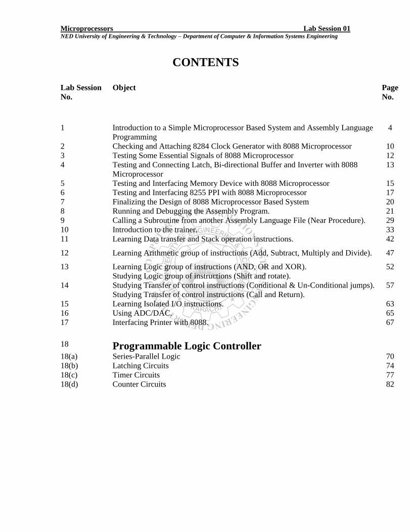
CONTENTS
Lab Session
No.
Object Page
No.
1 Introduction to a Simple Microprocessor Based System and Assembly Language
Programming 4
2 Checking and Attaching 8284 Clock Generator with 8088 Microprocessor 10
3 Testing Some Essential Signals of 8088 Microprocessor 12
4 Testing and Connecting Latch, Bi-directional Buffer and Inverter with 8088
Microprocessor
13
5 Testing and Interfacing Memory Device with 8088 Microprocessor 15
6 Testing and Interfacing 8255 PPI with 8088 Microprocessor 17
7 Finalizing the Design of 8088 Microprocessor Based System 20
8 Running and Debugging the Assembly Program. 21
9 Calling a Subroutine from another Assembly Language File (Near Procedure). 29
10 Introduction to the trainer. 33
11 Learning Data transfer and Stack operation instructions. 42
12 Learning Arithmetic group of instructions (Add, Subtract, Multiply and Divide). 47
13 Learning Logic group of instructions (AND, OR and XOR).
Studying Logic group of instructions (Shift and rotate).
52
14 Studying Transfer of control instructions (Conditional & Un-Conditional jumps).
Studying Transfer of control instructions (Call and Return).
57
15 Learning Isolated I/O instructions. 63
16 Using ADC/DAC. 65
17 Interfacing Printer with 8088. 67
18 Programmable Logic Controller
18(a) Series-Parallel Logic 70
18(b) Latching Circuits 74
18(c) Timer Circuits 77
18(d) Counter Circuits 82

Microprocessors Lab Session 01 NED University of Engineering & Technology – Department of Computer & Information Systems Engineering
4
Lab Session 01
OBJECT Introduction to a Simple Microprocessor Based System and Assembly Language
Programming THEORY
PROJECT DESCRIPTION
A simple microprocessor based system is to be designed and implemented step by step.
In this system there will be an input and output device in addition of a permanent storage
device interfaced with 8088 microprocessor. The list of components required for the
project is given here:
1. 8088 microprocessor
2. 8284 Clock Generator
3. 74373/74573 Latch
4. 74245 Bi-directional Buffer
5. 7404 Hex Invertor
6. 2716 EPROM / 2816 EEPROM
7. 8255 PPI
8. 8 bit DIP Switches pack
9. 8 LEDs
10. 1 crystal (15MHz)
11. 1 resistor (10KΩ)
12. 1 capacitor (10µF)
13. 1 diode (1N4001)
14. 1 Push Button Switch
15. 8 resistor (1KΩ)
16. Connecting wires
17. Vero board and Soldering Iron
ASSEMBLY LANGUAGE SYNTAX
name operation operand (s) comment
Assembly language statement is classified in two types
1. Instruction
Assembler translates into machine code.
Example:
START: MOV CX, 5 ; initialize counter
Comparing with the syntax of the Assembly statement, name field consists of the label
START:. The operation is MOV, operands are CX and 5 and the comment is ;initialize
counter.

Microprocessors Lab Session 01 NED University of Engineering & Technology – Department of Computer & Information Systems Engineering
5
2. Assembler Directive
Instructs the assembler to perform some specific task, and are not converted into
machine code.
Example:
MAIN PROC
MAIN is the name, and operation field contains PROC. This particular directive creates a
procedure called MAIN.
Name field
Assembler translate name into memory addresses. It can be 31 characters long.
Operation field
It contains symbolic operation code (opcode). The assembler translates symbolic
opcode into machine language opcode. In assembler directive, the operation field
contains a pseudo-operation code (pseudo-op). Pseudo-op are not translated into machine
code, rather they simply tell the assembler to do something.
Operand field
It specifies the data that are to be acted on by the operation. An instruction may
have a zero, one or two operands.
Comment field
A semicolon marks the beginning of a comment. Good programming practice
dictates comment on every line
Examples: MOVCX, 0 ;move 0 to CX
Do not say something obvious; so:
MOV CX, 0 ;CX counts terms, initially 0
Put instruction in context of program
; initialize registers
INPUT AND OUTPUT USING DOS ROUTINES
CPU communicates with peripherals through I/O registers called I/O ports. Two
instructions access I/O ports directly: IN and OUT. These are used when fast I/O is
essential, e.g. games.
Most programs do not use IN/OUT instructions. Since port addresses vary among
computer models and it is much easier to program I/O with service routines provided
by manufacturer.
Two categories of I/O service routines are Basic input & output system (BIOS)
routines and Disk operating system (DOS) routines. Both DOS and BIOS routines are
invoked by INT (interrupt) instruction.
Microprocessors Lab Session 01 NED University of Engineering & Technology – Department of Computer & Information Systems Engineering
6
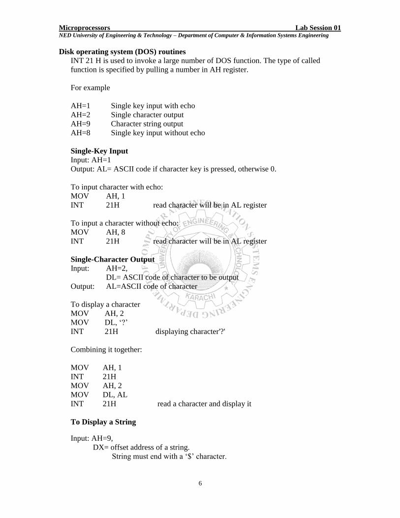
Disk operating system (DOS) routines
INT 21 H is used to invoke a large number of DOS function. The type of called
function is specified by pulling a number in AH register.
For example
AH=1 Single key input with echo
AH=2 Single character output
AH=9 Character string output
AH=8 Single key input without echo
Single-Key Input
Input: AH=1
Output: AL= ASCII code if character key is pressed, otherwise 0.
To input character with echo:
MOV AH, 1
INT 21H read character will be in AL register
To input a character without echo:
MOV AH, 8
INT 21H read character will be in AL register
Single-Character Output
Input: AH=2,
DL= ASCII code of character to be output
Output: AL=ASCII code of character
To display a character
MOV AH, 2
MOV DL, ‘?’
INT 21H displaying character'?'
Combining it together:
MOV AH, 1
INT 21H
MOV AH, 2
MOV DL, AL
INT 21H read a character and display it
To Display a String
Input: AH=9,
DX= offset address of a string.
String must end with a ‘$’ character.
Microprocessors Lab Session 01 NED University of Engineering & Technology – Department of Computer & Information Systems Engineering
7
To display the message Test Message!
MSG DB “Test Message!”
MOV AH, 9
MOV DX, offset MSG
INT 2IH
OFFSET operator returns the address of a variable. The instruction LEA (load
effective address) loads destination with address of source LEA DX, MSG
PROGRAM STRUCTURE
Machine language programs consist of code, data and stack. Each part occupies a
memory segment. Each program segment is translated into a memory segment by the
assembler.
Memory models
The size of code and data a program can have is determined by specifying a memory
model using the .MODEL directive. The format is:
.MODEL memory-model
Unless there is lot of code or data, the appropriate model is SMALL
memory-model description
SMALL One code-segment.
One data-segment.
MEDIUM
More than one code-segment.
One data-segment.
Thus code may be greater than 64K
COMPACT One code-segment.
More than one data-segment.
LARGE
More than one code-segment.
More than one data-segment.
No array larger than 64K.
HUGE
More than one code-segment.
More than one data-segment.
Arrays may be larger than 64K.
Data segment
A program’s DATA SEGMENT contains all the variable definitions.
To declare a data segment, we use the directive .DATA, followed by variable and
constants declarations.
.DATA
WORD1 DW 2
MASK EQU 10010010B
Microprocessors Lab Session 01 NED University of Engineering & Technology – Department of Computer & Information Systems Engineering
8
Stack segment
It sets aside a block of memory for storing the stack contents.
.STACK 100H ;this reserves 256 bytes for the stack
If size is omitted then by-default size is 1KB.
Code segment
Contain program’s instructions.
.CODE name
Where name is the optional name of the segment
There is no need for a name in a SMALL program, because the assembler will
generate an error). Inside a code segment, instructions are organised as procedures.
The simplest procedure definition is
name PROC
;body of message
name ENDP
An example
MAIN PROC
;main procedure instructions
MAIN ENDP
;other procedures go here
Putting it together
.MODEL SMALL
.STACK 100H
.DATA
;data definition go here
.CODE
MAIN PROC
;instructions go here
MAIN ENDP
;other procedures go here
END MAIN
The last line in the program should be the END directive followed by name of the
main procedure.

Microprocessors Lab Session 01 NED University of Engineering & Technology – Department of Computer & Information Systems Engineering
9
Program for the Project
TITLE PGM : 8255 PPI MODE 0 OPERATION
.MODEL SMALL
.CODE
MAIN PROC
MOV AL, 90h
OUT 03, AL
HERE: IN AL, 00
OUT 01, AL
JMP HERE
MAIN ENDP
END MAIN
Save above given program with name ‘project.asm’ in the folder where ‘masm.exe’ is
already present. Then, execute following command line from command prompt:
D:\MASM> masm project.asm
This command line will generate 3 files named ‘project.obj’, ‘project.lst’ and
‘project.crf’. Machine language for the above program can be noted from the list file.

Microprocessors Lab Session 02 NED University of Engineering & Technology – Department of Computer & Information Systems Engineering
10
Lab Session 02 OBJECT
Checking and Attaching 8284 Clock Generator with 8088 Microprocessor
THEORY
8284 Clock Generator:
There are three main sections within 8284 Clock Generator:
1. RESET Section
2. READY Section
3. CLOCK Section
RESET Section:
There is an input pin labeled as RES and an output pin labeled as RESET on the IC
package of 8284 Clock Generator. This section has an internal schmitt trigger. When
voltage level at RES input is less than a specific limit RESET is at logic 1. But, when
voltage level at RES input goes up a threshold, logic level at RESET output becomes
logic 0. When voltage level at RES input is greater than a specific limit RESET is at logic
0. But, when voltage level at RES input drops down a threshold, logic level at RESET
output becomes logic 1.
READY Section:
There are two ready input pins RDY1 and RDY2. These inputs may be used in
conjunction with AEN1 and AEN2 inputs for getting READY output from 8284.
READY pin of 8284 is to be connected with 8088 microprocessor’s READY input pin.
We may select one or two levels of synchronization by using ASYNC input pin present
on 8284 IC package.
CLOCK Section:
There are two methods of applying input frequency/clock to 8284 IC.
1. A crystal may be connected at input pins X1 and X2.
2. An external frequency generator source may be used for applying clock input at
EFI pin.
There are three different output clock signals generated by 8284 Clock Generator.
1. CLK: An output frequency of 1/3 rd of input frequency signal with duty cycle of
33%.
2. PCLK: An output frequency of 1/6 th of input frequency signal with duty cycle of
50%.
3. OSC: An output frequency of same as of input crystal connected at X1 and X2
inputs.

Microprocessors Lab Session 02 NED University of Engineering & Technology – Department of Computer & Information Systems Engineering
11
Checking 8284 Clock Generator after placing on Verobaord:
We have to use CLK and RESET outputs of 8284 Clock Generator. These two outputs
are to be connected with CLK and RESET inputs of 8088 microprocessor respectively.
For this purpose, you have to follow these steps:
1. Select a suitable place for soldering of 18-pin base near the place where you
intend to place 8088 microprocessor IC.
2. Connect pin 18 with common Vcc and pin 9 with common GND.
3. Connect 15 MHz crystal at X1 and X2 inputs.
4. Connect 10 KΩ resistor at RES input with second end connected to Vcc.
5. Connect anode of IN4001 diode at RES input with cathode connected to Vcc.
6. Connect positive end of 10 µF capacitor at RES input with second end connected
to GND.
7. Connect push button switch at RES input with second end connected to GND.
8. Connect F/C and CSYNC inputs with GND.
9. After applying +5V at Vcc and 0V at GND inputs check the signals present at
CLK and RESET outputs by using oscilloscope/frequency meter and multi-meter
respectively.
10. CLK output should have 5 MHz signal with duty cycle of 33%.
11. RESET output should have logic 0 signal initially until the push button switch
present at RES input is pressed for applying logic 0 at RES input. When RES is
having logic 0, logic 1 will appear at RESET output.
12. After checking CLK and RESET signals you may proceed to next step of
connecting these signals with 8088 microprocessor.
Microprocessors Lab Session 03 NED University of Engineering & Technology – Department of Computer & Information Systems Engineering
12
Lab Session 03 OBJECT
Testing Some Essential Signals of 8088 Microprocessor
THEORY Whenever Microprocessor is provided a clock signal of certain frequency then in
response microprocessor generates some important signals like ALE, DEN etc. As these
signals are generated in response of clock input therefore, frequency appeared at these
output pins are related to the frequency of clock input.
Frequency at ALE = 1/4 (Frequency at CLK)
Frequency at DEN = 1/4 (Frequency at CLK)
If we want to check the working condition of 8088 Microprocessor then we may measure
the frequency or view the wave shape appearing at these output pins.
How to Check ALE and DEN:
1. You have to select a suitable portion for placing 40-pin base of 8088
Microprocessor on your veroboard. Placement of 40-pin base should be next to
18-pin base of 8284 Clock Generator.
2. Connect CLK output of 8284 Clock Generator to the CLK input of 8088
Microprocessor.
3. Connect RESET output of 8284 Clock Generator to the RESET input of 8088
Microprocessor.
4. Now connect pins 1 and 20 to GND and pin 40 to Vcc.
5. Connect INTR, NMI and HOLD pins to GND and MN/MX, READY inputs to
Vcc.
6. Now connect a wire with ALE pin and another wire with DEN pin.
7. After that, apply power (Vcc and GND) to the 8284 Clock Generator and 8088
Microprocessor ICs and view the signals on oscilloscope present at CLK, ALE
and DEN pins of 8088 Microprocessor.
8. As the connected crystal with X1 and X2 inputs of 8284 Clock Generator is of 15
MHz. So, CLK pin should have 5 MHz frequency signal. Accordingly, each one
of ALE and DEN pins should have 1.25 MHz frequency signals.
9. If the frequencies mentioned in No.8 can be viewed on oscilloscope then 8088
Microprocessor IC is most probably in good working condition.

Microprocessors Lab Session 04 NED University of Engineering & Technology – Department of Computer & Information Systems Engineering
13
Lab Session 04 OBJECT
Testing and Connecting Latch, Bi-directional Buffer and Inverter with 8088
Microprocessor
THEORY
74373/74573 Latch:
Latch is used to temporarily store addresses until latch is disabled. There are 20 pins on
the IC package of 74373 Latch. There are 8 input pins and 8 output pins. In addition of
these pins, there are Vcc, GND, LE and OE pins on the IC package.
74245 Bi-directional Buffer:
Buffer is used to enhance the signal strength as well as to isolate microprocessor data bus
from the system bus. There are 20 pins on the IC package of 74245 bi-directional buffer.
There are two sides (say side A and side B) for connecting 8 bit data buses of different
devices. At Side A (A7 – A0) data bus of 8088 microprocessor is connected. While at
Side B (B7 – B0) data buses of remaining devices are connected. In addition of these
pins, there are Vcc, GND, DIR and G pins on the IC package.
7404 Hex Inverter:
Inverter is used for toggling the inputted logic signal. If logic 1 is applied at input then
logic 0 will appear at output. If logic 0 is applied at input then logic 1 will appear at
output. This IC has 6 inverters in it.
Checking Procedure for Latch:
For checking the working condition of a latch IC, these steps are to be followed:
1. Connect 8 pins of input side to an 8 DIP Switches pack.
2. Connect 8 LEDs at the output pins of latch.
3. Connect Vcc and GND input pins with +5V and 0V respectively.
4. Connect OE pin with GND for enabling output from latch IC.
5. Connect LE pin with Vcc for enabling the IC. When this pin is connected with
GND latch will be disabled.
Checking Procedure for Bi-directional Buffer:
For checking the working condition of Bi-directional buffer IC, these steps are to be
followed:
3. Connect 8 pins of side A to an 8 DIP Switches pack.
4. Connect 8 LEDs at the side B data pins.
5. Connect Vcc and GND input pins with +5V and 0V respectively.
6. Connect G pin with GND for enabling buffer IC.
7. Connect DIR pin with Vcc for set direction of data flow from side A to side B.
8. Now exchange the place of DIP Switches and LEDs. In this case DIR will be
connected with GND and data will flow from side B to side A.

Microprocessors Lab Session 04 NED University of Engineering & Technology – Department of Computer & Information Systems Engineering
14
Checking Procedure for Inverter:
For checking the working condition of inverters present in inverter IC, these steps are to
be followed:
1. Connect Vcc and GND input pins with +5V and 0V respectively.
2. There are 6 independent inverters in this IC placed between pins 1,2 and 3,4 and
5,6 and 13,12 and 11,10 and 9,8.
3. Apply logic 1/0 at pin 1 and check the logic level present at pin 2 by attaching a
LED. If there is logic 0/1 present that shows inverter is working properly.
4. Repeat step 3 for remaining 5 inverters.
Placing Latch and Buffer ICs on Veroboard:
Address/Data multiplexed bus (AD7 – AD0) is to be connected with latch and buffer ICs.
For this purpose, you have to follow these steps:
1. Select a suitable place for soldering two 20-pin bases near the place where you
have placed 8088 microprocessor IC.
2. Connect pin 20 of both ICs with common Vcc and pin 10 of both ICs with
common GND.
3. Connect AD7 – AD0 pins of 8088 microprocessor with input address pins of latch
IC.
4. Connect AD7 – AD0 pins of 8088 microprocessor with side A of bi-directional
buffer IC.
5. Connect OE and LE pins of latch with GND and ALE of 8088 microprocessor
respectively.
6. Connect G and DIR pins of bi-directional buffer with DEN and DT/R of 8088
microprocessor respectively.
Placing Inverter IC on Veroboard:
1. Select a suitable place for soldering 14 pin base between the space present
between 8088 microprocessor and 8255 PPI (to be connected next).
2. Connect pin 14 and pin 7 of IC with common Vcc and common GND.
3. Connect IO/M signal from 8088 microprocessor to the input of any one of the
inverter’s present in 7404 IC.
4. Output of the used inverter is to be connected later to some pin of 8255 PPI IC.

Microprocessors Lab Session 05 NED University of Engineering & Technology – Department of Computer & Information Systems Engineering
15
Lab Session 05 OBJECT
Testing and Interfacing Memory Device with 8088 Microprocessor
THEORY
Memory Devices:
There are two main types of memory devices:
1. Volatile Memory Devices: These devices retain data stored for the period during
which power is applied.
2. Non-volatile Memory Devices: These devices retain data stored whether power in
applied or not.
Memory Device in Microprocessor based System:
Because of the fact that microprocessor doesn’t have internal memory for storing
instruction and data. Therefore, there must be an external permanent storage device
interfaced with microprocessor for storing instructions. Microprocessor generates
addresses and in response it gets instructions through data bus for execution from that
non-volatile storage device.
Here, we have to interface a 2716 EPROM with 8088 Microprocessor. Before we
interface EPROM, we have to check its function.
How to Check EPROM:
2716 EPROM has capacity of 2kB. That means, there are 2k locations and at each
location a byte (8 bit) is stored. For addressing 2k locations 11 address lines are required.
Therefore, there are 11 address lines and 8 data lines. In addition of these address and
data lines, there are Vcc and GND pins for power connection of +5V and 0V
respectively. Furthermore, there are CE (chip enable) and OE (output enable) pins on the
package of 2716. Both of these are input pins. For enabling the chip CE must be having
logic 0 applied and for taking output form data bus OE must be applied with logic 0.
Before we check 2716 EPROM there must be some known data present in the device. For
that, we have to program EPROM device with following simple program’s machine
language.
Assembly Instructions Machine Language
MOV AL, 90h B0 90
OUT 03, AL E6 03
HERE: IN AL, 00 E4 00
OUT 01, AL E6 01
JMP HERE EB FA
Whenever 8088 microprocessor starts, it generates first 20 bit address FFFF0h. But, we
have discussed earlier that there are only 11 address lines on the IC package of 2716
EPROM. That means, 2716 will get first address from microprocessor 7F0h. Therefore,
we must store our program starting from address 7F0h in 2716 EPROM.
Microprocessors Lab Session 05 NED University of Engineering & Technology – Department of Computer & Information Systems Engineering
16
After storing program in 2716 EPROM by using EPROM programmer we have to read
data from different addresses for confirmation of the working condition of EPROM
device. For that purpose, you have to follow these steps:
1. Place 2716 on breadboard and apply Vcc and GND signals.
2. Then apply pattern of 7F0h on address bus. For that, you have to connect address
lines A0, A1, A2 and A3 to logic 0 (GND) and remaining address lines A10 - A4
will be connected to logic 1 (Vcc).
3. Now connect an LED on each data line (D7 - D0) present on the IC of 2716 with
second end grounded.
4. After that apply logic 0 at CE pin to enable the 2716 IC for read operation.
5. Check the pattern present on LEDs after applying logic 0 at OE pin of 2716 IC.
Pattern should be like this:
D7 D6 D5 D4 D3 D2 D1 D0
1 0 1 1 0 0 0 0 : B0h
Now, repeat above given steps for addresses from 7F1h to 7F9h for confirmation of data
stored.
Implementation on Veroboard:
You have to implement the connections between Microprocessor 8088 and EPROM 2716
on Veroboard. These are the steps involved:
1. Select a suitable place for soldering of 24-pin base near address latch and data
buffer ICs.
2. Connect pin 24 with common Vcc and pin 12 with common GND.
3. 2716 EPROM has 11 address lines (A10 – A0). First 7 address lines (A7 – A0)
are to be picked from the output of address latch. Remaining address lines (A10 –
A8) will be connected directly from microprocessor to EPROM.
4. 2716 EPROM has 8 data lines (D7 – D0). These pins are to be connected to data
buffer side B pins.
5. CE pin of 2716 EPROM is to be connected with IO/M of 8088 Microprocessor.
6. OE pin of 2716 EPROM is to be connected with RD of 8088 Microprocessor.
Microprocessors Lab Session 06 NED University of Engineering & Technology – Department of Computer & Information Systems Engineering
17
Lab Session 06 OBJECT
Testing and Interfacing 8255 PPI with 8088 Microprocessor
THEORY
8255 Programmable Peripheral Interface:
There are three 8 bit ports available for interfacing I/O devices on the IC package of 8255
PPI. These three ports may be divided in two groups. Three modes of operation are
available. User will select the desired mode according to the requirement. Command Byte
A is used to select the desired mode of operation. After that Command Byte A pattern is
outputted to the address of command register. There are two address inputs available on
the IC package for the selection as shown in the following table.
Modes of Operation:
1. Mode 0: All the three ports A, B and C are used independently for data input or
output.
2. Mode 1: Port A and Port B may be programmed for strobed data input or buffered
data output operations. Port C bits will serve as control signals for facilitating the data
transfer through Ports A and B.
3. Mode 2: Port A may only be used in this mode with Port C having the handshaking
signals required for the bi-directional data transfer.
Command Byte A:
1 Mode Group A Port A PA7 – PA0
Port C PC7 – PC4
Mode Group B
Port B PB7 – PB0
Port C PC3 – PC0
7 6 5 4 3 2 1 0
8255 PPI in Our Project:
In our project, we have to interface a simple input device (DIP Switches pack) and an
output device (8 LEDs) on Ports A and B of 8255 PPI. Mode 0 is suitable for interfacing
A1 A0 Select
0 0 Port A
0 1 Port B
1 0 Port C
1 1 Command Register

Microprocessors Lab Session 06 NED University of Engineering & Technology – Department of Computer & Information Systems Engineering
18
simple I/O devices. Therefore, here we have to initialize Ports A and B for mode 0
operation.
How to Check 8255 PPI:
For checking 8255 PPI following steps are to be followed:
1. Place 8255 IC on breadboard and apply Vcc and GND signals.
2. Connect CS input pin with GND for enabling the IC of 8255 PPI.
3. Before we can use ports of 8255 PPI as input or output, we have to write command
byte to the command register address of 8255 PPI.
4. An input device is to be connected with Port A and an output device is to be
connected with Port B.
5. 8 bit Command Byte A pattern for the required configuration is: 1 0 0 1 x 0 0 x.
By replacing don’t cares with zero ‘0’ we get 1 0 0 1 0 0 0 0 = 90h.
6. This 90h is to be written at output port address 03h. 03h is the address that selects
command register as A1, A0 address lines have pattern 1, 1.
7. For applying logic ‘1’ at A0 and A1 pins of 8255 PPI, connect both pins to Vcc.
8. Now apply pattern 90h at data input lines D7 – D0.
9. After that apply logic ‘0’ at WR pin of 8255 PPI for writing the command byte to
command register.
10. Now, change the pattern at A1, A0 address inputs to 0, 1 for selecting Port B.
11. At Port B pins (PB7 – PB0) connect 8 LEDs to display output.
12. Apply some known pattern at data lines D7 – D0. The same pattern should appear
at LEDs until WR is at logic 0.
13. Now, change the pattern at A1, A0 address inputs to 0, 0 for selecting Port A.
14. At data lines D7 – D0 connect 8 LEDs to display output.
15. Apply some known pattern at Port A pins (PA7 – PA0). The same pattern should
appear at LEDs until RD is at logic 0.
Implementation on Veroboard:
These are the steps to implement the connections between Microprocessor 8088 and 8255
PPI on Veroboard.:
1. Select a suitable place for soldering of 40-pin base near address latch and data
buffer ICs.
2. Connect pin 26 with common Vcc and pin 7 with common GND.
3. 8255 PPI has 2 address lines (A1 – A0). These address lines will be connected
from the output of Address Latch. A1 and A0 from the output of address latch are
to be connected to A1 and A0 of 8255 PPI.
4. 8255 PPI has 8 data lines (D7 – D0). These pins are to be connected to data buffer
side B pins.
5. CS pin of 8255 PPI is to be connected with IO/M of 8088 Microprocessor through
an inverter of 7404 Hex Inverter IC.

Microprocessors Lab Session 06 NED University of Engineering & Technology – Department of Computer & Information Systems Engineering
19
6. RESET, RD and WR pins of 8255 PPI are to be connected with RESET, RD and
WR pins of 8088 Microprocessor respectively.
7. 8 bit DIP Switch pack is to be connected with Port A of 8255. If Side A of DIP
Switches are connected with Port A then Side A pins are to be grounded through
1KΩ resistors and Side B of DIP Switches are to be connected directly to Vcc.
8. Anode of 8 LEDs are to be connected with Port B pins of 8255 PPI with cathode
grounded.
Microprocessors Lab Session 08 NED University of Engineering & Technology – Department of Computer & Information Systems Engineering
20
Lab Session 07 OBJECT
Finalizing the Design of 8088 Microprocessor Based System
THEORY Up till now, we have checked operation of following components one by one:
1. 8284 Clock Generator
2. 8088 Microprocessor
3. 74373 Latch, 74245 Bi-directional Buffer and 7404 Invertor.
4. 2716 EPROM
5. 8255 PPI
Now, we have to operate the circuit as a whole. For finalizing the design of circuit, these
checking steps is further required:
1. All the connections of Vcc must be connected to a common Vcc point.
2. All the connections of GND must be connected to a common GND point.
Check the circuit as a whole:
1. Now apply the supply voltages +5V at common Vcc and 0V at common GND
points on veroboard.
2. Set a specific pattern on Port A by selecting ON/OFF position of DIP Switches.
3. Whatever 8 bit ON/OFF pattern is applied through DIP Switches. That should
appear on 8 LEDs connected on Port B.
4. Now, change the applied pattern at DIP Switches and pattern at LEDs will be
changed accordingly.
5. Push Button Switch connected with RESET input may be pressed for manually
resetting the circuit.
6. By getting the desired operation we have implemented the basic circuit of
interfacing a single memory device and one input and output device with
microprocessor.
Checking Other Features:
Now, you may work further for:
1. Interfacing RAM device with 8088 Microprocessor.
2. Implementing Interrupt Structure of 8088 Microprocessor
3. Implementing DMA Operation of the 8088 Microprocessor.
4. Interfacing more complex I/O devices with 8088 Microprocessor.

Microprocessors Lab Session 08 NED University of Engineering & Technology – Department of Computer & Information Systems Engineering
21
Lab Session 08 OBJECT
Running and Debugging the Assembly Program
THEORY A Case Conversion Program
Prompt the user to enter a lowercase letter, and on next line displays another message
with letter in uppercase, as:
Enter a lowercase letter: a
In upper case it is: A
TITLE PGM4_1: CASE CONVERSION PROGRAM
.MODEL SMALL
.STACK 100H
.DATA
CR EQU 0DH
LF EQU 0AH
MSG1 DB 'ENTER A LOWER CASE LETTER: $'
MSG2 DB CR, LF, 'IN UPPER CASE IT IS: '
CHAR DB ?,'$'
.CODE
MAIN PROC
;initialize DS
MOV AX,@DATA ; get data segment
MOV DS,AX ; initialize DS
;print user prompt
LEA DX,MSG1 ; get first message
MOV AH,9 ; display string function
INT 21H ; display first message
;input a character and convert to upper case
MOV AH,1 ; read character function
INT 21H ; read a small letter into AL
SUB AL,20H ; convert it to upper case
MOV CHAR,AL ; and store it
;display on the next line
LEA DX,MSG2 ; get second message
MOV AH,9 ; display string function
INT 21H ; display message and upper case letter in front
;DOS exit
MOV AH,4CH ; DOS exit
INT 21H
MAIN ENDP
END MAIN
Save your program with (.asm) extension.
Microprocessors Lab Session 08 NED University of Engineering & Technology – Department of Computer & Information Systems Engineering
22
If “first” is the name of program then save it as “first.asm”
ASSEMBLING THE PROGRAM Assembling is the process of converting the assembly language source program into machine language
object file. The program “ASSEMBLER” does this.
Assemble the program
C:\>masm first.asm Microsoft (R) Macro Assembler Version 5.10
Copyright (C) Microsoft Corp 1981, 1988. All rights reserved.
Object filename [first.OBJ]: first
Source listing [NUL.LST]: first
Cross-reference [NUL.CRF]: first 47338 + 430081 Bytes symbol space free
0 Warning Errors
0 Severe Errors
After assembling the program as shown above you will find two additional files with the object file,
automatically generated by the assembler, in your directory i.e. the list file and the cross-reference file.
Name must be provided for .LST else NUL (nothing) will be generated.
1. OBJECT FILE A non-executable file contains the machine code translation of assembly code, plus other information
needed to produce the executable.
2. LIST FILE The list file is a text file that gives you assembly language code and the corresponding machine language
code, a list of names used in the program, error messages and other statistics as shown below for the
assembly file first.asm:
PGM4_1: CASE CONVERSION PROGRAM Page 1-1
1 TITLE PGM4_1: CASE CONVERSION PROGRAM
2 .MODEL SMALL
3 .STACK 100H
4 .DATA
5 = 000D CR EQU

Microprocessors Lab Session 08 NED University of Engineering & Technology – Department of Computer & Information Systems Engineering
23
0DH
6 = 000A LF EQU
0AH
7 0000 45 4E 54 45 52 20 MSG1 DB 'ENTER A LOWER
CASE LETTER: $'
8 41 20 4C 4F 57 45
9 52 20 43 41 53 45
10 20 4C 45 54 54 45
11 52 3A 20 20 24
12 001D 0D 0A 49 4E 20 55 MSG2 DB 0DH, 0AH, 'IN U
PPER CASE IT IS: '
13 50 50 45 52 20 43
14 41 53 45 20 49 54
15 20 49 53 3A 20 20
16 0035 00 24 CHAR DB ? ,'$'
17 .CODE
18 0000 MAIN PROC
19 ; initialize DS
20 0000 B8 ---- R MOV AX,@DATA ; get data segment
21 0003 8E D8 MOV DS, AX ; initialize DS
22 ;print user prompt
23 0005 8D 16 0000 R LEA DX,MSG1 ; get first message
24 0009 B4 09 MOV AH,9 ; display string
function
25 000B CD 21 INT 21H ; display first
message
26 ;input a character and
;convert to uppercase
27 000D B4 01 MOV AH,1 ; read character
function
28 000F CD 21 INT 21H ;read a small letter
into AL
29 0011 2C 20 SUB AL,20H ; convert it to upper case
30 0013 A2 0035 R MOV CHAR,AL ; and store it
31 ;display on the next line
32 0016 8D 16 001D R LEA DX,MSG2 ;get second message
33 001A B4 09 MOV AH,9 ; display string
function
34 001C CD 21 INT 21H ; display message and
;upper case letter in front
35 ;DOS exit
PGM4_1: CASE CONVERSION PROGRAM Page 1-2
36 001E B4 4C MOV AH,4CH ; DOS e
xit
37 0020 CD 21 INT 21H
38 0022 MAIN ENDP
39 END MAIN

Microprocessors Lab Session 08 NED University of Engineering & Technology – Department of Computer & Information Systems Engineering
24
PGM4_1: CASE CONVERSION PROGRAM Symbols-1
Segments and Groups:
N a m e Length Align Combine Class
DGROUP . . . . . . . . . . . . . GROUP
_DATA . . . . . . . . . . . . . 0037 WORD PUBLIC 'DATA'
STACK . . . . . . . . . . . . . 0100 PARA STACK 'STACK'
_TEXT . . . . . . . . . . . . . . 0022 WORD PUBLIC 'CODE'
Symbols:
N a m e Type Value Attr
CHAR . . . . . . . . . . . . . . . . . . L BYTE 0035 _DATA
CR . . . . . . . . . . . . . . . . . . . . . NUMBER 000D
LF . . . . . . . . . . . . . . . . . . . . . NUMBER 000A
MAIN . . . . . . . . . . . . . . . . . . N PROC 0000 _TEXT Length = 0022
MSG1 . . . . . . . . . . . . . . . . . . L BYTE 0000 _DATA
MSG2 . . . . . . . . . . . . . . . . . . L BYTE 001D _DATA
@CODE . . . . . . . . . . . . . . . . TEXT _TEXT
@CODESIZE . . . . . . . . . . . . TEXT 0
@CPU . . . . . . . . . . . . . . . . . . TEXT 0101h
@DATASIZE . . . . . . . . . . . . TEXT 0
@FILENAME . . . . . . . . . . . . TEXT cc
@VERSION . . . . . . . . . . . . TEXT 510
32 Source Lines
32 Total Lines
23 Symbols
46146 + 447082 Bytes symbol space free
0 Warning Errors
0 Severe Errors
3. CROSS-REFERENCE FILE List names used in the program and the line number.
LINKING THE PROGRAM Linking is the process of converting the one or more object files into a single executable file. The program
“LINKER” does this.
Microprocessors Lab Session 08 NED University of Engineering & Technology – Department of Computer & Information Systems Engineering
25
C:\>link first.obj; Microsoft (R) Overlay Linker Version 3.64
Copyright (C) Microsoft Corp 1983-1988. All rights reserved.
RUNNING THE PRORAM On the command line type the name of the program to run.
C:\>first.exe ENTER A LOWER CASE LETTER: a
IN UPPER CASE IT IS: A
DEBUGGING DEBUG is a primitive but utilitarian program, supplied with MS-DOS, with a small easy to learn command
set. After assembling and linking the program in previous practical, (first.asm) we take the first.exe into
DEBUG. On the MS-DOS prompt type the following command,
_____________________________
C:\>DEBUG first.exe
-
________________________
DEBUG comes back with its “-“command prompt.
To view registers and FLAGS, type “R‟
C:\>debug first.exe
-R AX=0000 BX=0000 CX=0030 DX=0000 SP=0100 BP=0000 SI=0000 DI=0000
DS=1189 ES=1189 SS=119C CS=1199 IP=0000
NV UP EI PL NZ NA PO NC

Microprocessors Lab Session 08 NED University of Engineering & Technology – Department of Computer & Information Systems Engineering
26
1199:0000 B89A11 MOV AX,119A
-
As we know 8086 has 14 registers, all of these registers are shown by DEBUG with different values stored
in these registers.
FLAG REGISTER
The letters pairs on the fourth line are the current setting of some of the status and control FLAGS. The
FLAGS displayed and the symbols DEBUG uses are the following:
To change the contents of a register-for example, AX to 1245h ____________________________
-RDX DX 0000
:1245 _______________________
Note:- DEBUG assumes that all numbers are expressed in hex. Now let us verify the
change, through “R‟ command.
DX now contain 1245h. The next instruction to be executed by the CPU is written on the last line with its address in the memory.
Let us execute each instruction one by one using „T‟ trace command. But before that, just check whether
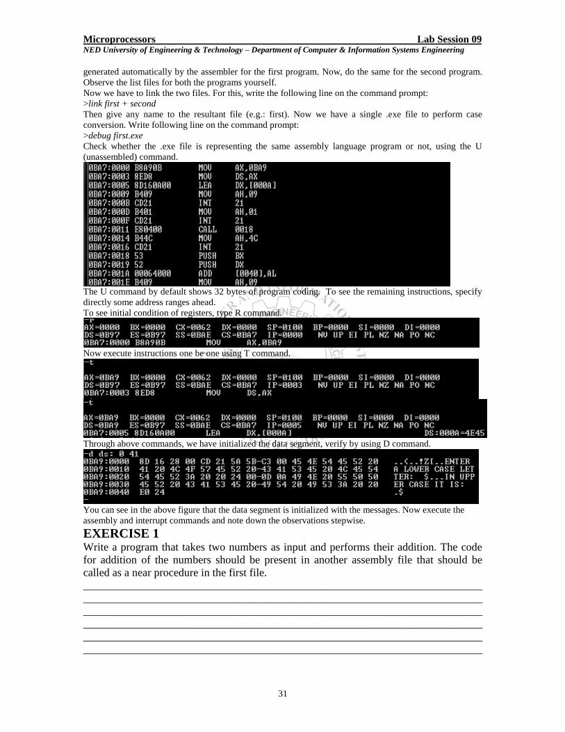
the “.exe‟ file is representing the same assembly language program or not, using the U (unassembled)
command.
Microprocessors Lab Session 08 NED University of Engineering & Technology – Department of Computer & Information Systems Engineering
27
The U command by default shows 32 bytes of program coding. The last instruction shown above is not our
last program’s instruction. To see the remaining instructions, specify directly some address ranges ahead.
Now execute instructions one be one using T command.
AX now have the segment number of the data segment. Again press T for one more time will execute the
instruction MOV DS, AX as shown on the last line above. This will initialize the data segment register with
the data segment address of the program.
The next command LEA DX, [0002] will load the offset address of MSG1 in DX which is 0002.
Check the contents of the data segment using the D command:
We can see that the string variables initialized in the Data Segment has been successfully loaded into the
memory locations as above. Now through MOV AH, 09 and interrupt command -g 000d, MSG1will be displayed as shown below:
Pressing T one more time will move 01 in AH so that we can take input.

Microprocessors Lab Session 08 NED University of Engineering & Technology – Department of Computer & Information Systems Engineering
28
Now through interrupt command -g 0011, user will be prompted to enter a lower case letter As you can
see, ‘a’ is entered as input, so AX will now contain 0161 where 61 is the ASCII code of
‘a’.
Now the SUB command will subtract 20 out of the contents of AL to perform case
conversion.
Again pressing ‘t’ will store the case conversion output i.e. ‘A’ in memory. Now to display MSG2, its offset address will be loaded in DX:
MOV AH, 09 and interrupt command are used to print the string on screen as done before. The result will
be displayed as follows:
This message indicates that the program has run to completion. The program must be reloaded to execute
again. Now leave the DEBUG using “Q‟,

Microprocessors Lab Session 09 NED University of Engineering & Technology – Department of Computer & Information Systems Engineering
29
Lab Session 09
OBJECT
Calling a subroutine from another assembly file as a near procedure
THEORY
Near call—A call to a procedure within the current code segment (the segment currently pointed to by the
CS register), sometimes referred to as an intrasegment call.
Procedure Declaration
The syntax of procedure declaration is the following:
PROC name NEAR
; body of procedure
ret
ENDP name
The CALL Instruction
CALL invokes a procedure
call name
where name is the name of a procedure.
Executing a CALL
The return address to the calling program (the current value of the IP) is saved on the stack
IP get the offset address of the first instruction of the procedure (this transfers control to the
procedure)
The RET instruction
To return from a procedure, the instruction
ret pop_value is executed.
The integer argument pop_value is optional.
ret causes the stack to be popped into IP.
A Case Conversion Program Prompt the user to enter a lowercase letter, and on next line displays another message with letter in
uppercase, as: Enter a lowercase letter: a
In upper case it is: A
We will create two different assembly files to implement case conversion. First file contains the code that
will prompt user to enter a lower case letter. This file contains a call to a near procedure named
CONVERT, which is used to perform case conversion. The second file contains the code of the procedure
CONVERT. So, when the procedure CONVERT is invoked, the given lower case letter will be converted
to upper case. The control will then be returned back to the calling procedure in the first file which will
display the output.
Assembly code for both of the files is given below:
TITLE PGM4_2: CASE CONVERSION EXTRN CONVERT: NEAR .MODEL SMALL

Microprocessors Lab Session 09 NED University of Engineering & Technology – Department of Computer & Information Systems Engineering
30
.STACK 100H
.DATA MSG DB 'ENTER A LOWER CASE LETTER: $' .CODE MAIN PROC MOV AX,@DATA ; get data segment MOV DS,AX ; initialize DS ;print user prompt LEA DX,MSG ; get first message MOV AH,9 ; display string function INT 21H ; display first message ;input a character and convert to upper case MOV AH,1 ; read character function INT 21H ; read a small letter into AL CALL CONVERT ; convert to uppercase MOV AH,4CH INT 21H ;DOS exit MAIN ENDP END MAIN
Save your program with (.asm) extension. If “first” is the name of program then save it
as “first.asm”.
TITLE PGM4_2A : CASE CONVERSION PUBLIC CONVERT .MODEL SMALL .DATA MSG DB 0DH, 0AH, 'IN UPPER CASE IT IS: ' CHAR DB -20H,'$' .CODE CONVERT PROC NEAR ;converts char in AL to uppercase PUSH BX PUSH DX ADD CHAR,AL MOV AH,9 LEA DX,MSG INT 21H POP DX POP BX RET CONVERT ENDP END
Save the above program as well with (.asm) extension. If “second” is the name of
program then save it as “second.asm”. Now follow the steps as mentioned in the previous lab session to assemble the two files. First perform all
the steps to assemble and create .obj file for the first program, list file and cross reference file will also be
Microprocessors Lab Session 09 NED University of Engineering & Technology – Department of Computer & Information Systems Engineering
31
generated automatically by the assembler for the first program. Now, do the same for the second program.
Observe the list files for both the programs yourself. Now we have to link the two files. For this, write the following line on the command prompt:
>link first + second
Then give any name to the resultant file (e.g.: first). Now we have a single .exe file to perform case
conversion. Write following line on the command prompt:
>debug first.exe Check whether the .exe file is representing the same assembly language program or not, using the U
(unassembled) command.
The U command by default shows 32 bytes of program coding. To see the remaining instructions, specify
directly some address ranges ahead.
To see initial condition of registers, type R command.
Now execute instructions one be one using T command.
Through above commands, we have initialized the data segment, verify by using D command.
You can see in the above figure that the data segment is initialized with the messages. Now execute the
assembly and interrupt commands and note down the observations stepwise.
EXERCISE 1 Write a program that takes two numbers as input and performs their addition. The code
for addition of the numbers should be present in another assembly file that should be
called as a near procedure in the first file.
________________________________________________________________________
________________________________________________________________________
________________________________________________________________________
________________________________________________________________________
________________________________________________________________________
________________________________________________________________________

Microprocessors Lab Session 09 NED University of Engineering & Technology – Department of Computer & Information Systems Engineering
32
________________________________________________________________________
________________________________________________________________________
________________________________________________________________________
________________________________________________________________________
________________________________________________________________________
________________________________________________________________________
________________________________________________________________________
________________________________________________________________________
________________________________________________________________________
________________________________________________________________________
________________________________________________________________________
________________________________________________________________________
________________________________________________________________________
________________________________________________________________________
________________________________________________________________________
________________________________________________________________________
________________________________________________________________________
________________________________________________________________________
________________________________________________________________________
________________________________________________________________________
________________________________________________________________________
________________________________________________________________________
________________________________________________________________________
________________________________________________________________________
________________________________________________________________________
________________________________________________________________________
________________________________________________________________________
________________________________________________________________________
________________________________________________________________________
________________________________________________________________________
________________________________________________________________________
________________________________________________________________________
________________________________________________________________________
________________________________________________________________________
________________________________________________________________________
________________________________________________________________________
________________________________________________________________________
________________________________________________________________________
________________________________________________________________________
________________________________________________________________________
________________________________________________________________________
________________________________________________________________________
________________________________________________________________________
________________________________________________________________________
________________________________________________________________________
________________________________________________________________________
Microprocessors Lab Session 10 NED University of Engineering & Technology – Department of Computer & Information Systems Engineering
33
Lab Session 10
OBJECT
Introduction to the trainer.
THEORY
The MC 8088/EV microcomputer trainer is a microprocessor controlled educational
system, based on 8088, conceived to face any problem concerning the study and use of
microprocessor systems.
The 8088 is one of the most common microprocessors and so it can be of help for
studying the structure and general function of PCs. Consequently a fundamental step in
the evolution of PCs is the introduction, by IBM of this kind of microprocessor into the
PC “IBM PC” in 1981.
The basic MC8088/EV contains all the necessary components for the study of this kind of
systems (8088 microprocessor, RAM and EPROM memory, liquid crystal display and
keyboard, serial and parallel interface, analog inputs and outputs, troubleshooting
section).
Technical characteristics of the trainer are:
8088/4.77 MHz microprocessor;
16 Kbytes system EPROM;
16*2 Kbyte user EPROM;
2 Kbyte RAM memory expandable to 6 Kbyte;
Keyboard (USA type PC keyboard);
Liquid crystal display (max 40 characters : 2 lines with 20 characters each);
Buzzer;
Cassette recorder interface;
CENTRONICS parallel interface;
8 bit IN/OUT parallel ports;
serial interface (standard RS-232);
BUS expansion interface;
Analog output with 8-bit D/A converter;
Analog input with 8-bit A/D converter;
Device for troubleshooting (Num.max.=8);
8+2 logic probes for fault insertion;
Power supplies: 5V/3A, +/-12V/0.3A;
EPROM monitor with:
Register display and edit
Memory display and edit
Continuous, step-by-step, break-points program run

Microprocessors Lab Session 10 NED University of Engineering & Technology – Department of Computer & Information Systems Engineering
34
Load and save on cassette recorder.
General operation:
All the system’s operations are controlled by microprocessor 8088 (IC1). The clock is
generated by an oscillator composed by inverters TTL-7404 (IC15) and by the system
quartz (14.318 MHz). With the two J-K flip flops included in IC 74107 the original
frequency is divided to obtain the microprocessor clock.
The general RESET line, used by UART also, is short circuited to ground by a condenser
switching on the system (logic level “0”) while this line returns to logic level “1” after
few m-seconds.
The data, addresses and control lines bus are buffered with ICs type 74244, 74245 and
74373 (IC3, IC2, IC4, IC8, IC16).
The selection among the devices concerned with the processor (EPROM memory, RAM,
I/O ports…) is made by ICs type IC17, IC19, IC21, IC22, IC23 and IC24.
These components type 74139 and 74138 are line decoders, 21N – 4OUT and 3IN –
8OUT respectively. The logic combination of the two or three input lines selects one of
the four or eight possible outputs and the selected device because these lines are
connected to the devices enable ones.
Using the Trainer
The monitor commands are given below:
Command
Name Purpose Syntax
A Assembler To let the user to type
8088 assembly language
programs into memory
and assemble them into
machine code line by
line.
(1) A
(2) A <addr>
L
Disassembler
To translate
(disassemble) a block of
memory into 8088
assembly instructions.
(1)
(2) L
(3) L <addr1>
(4) L <addr1> / <n>
(5) L <addr1> <addr2>
G
Go
To execute a program in
memory.
(1)
(2) G
(3) G <addr>
S Step
To single-step a
program or execute a
(1)
(2) S
(3) S n

Microprocessors Lab Session 10 NED University of Engineering & Technology – Department of Computer & Information Systems Engineering
35
specified number of
instructions and then
stop with a display of
register contents on the
screen; execution starts
from the address pointed
to by the CS regirter and
the IP register.
B
Breakpoint
To set up to three
breakpoints or display
their current settings.
When a program is on
execution and runs into
a breakpoint address, the
program execution will
be halted.
(1)
(2) B
(3) B <n>
(4) B <n> <addr>
C
Cancel
Breakpoint
To cancel one or all of
the breakpoints set
previously.
(1)
(2) C
(3) C <n>
X
Register
To display or change the
contents of any of the
registers.
(1)
(2) X
(3) X <register name>
M
Memory
To display or change the
contents of a memory
location or a range of
memory location.
(1)
(2) M
(3) M <addr1>
(4) M <addr1> <addr2>
(5) M <addr1> <addr2> /
<data1> /
I
Insert
To insert data into a
memory location or a
portion of memory
locations.
(1)
(2) I
(3) I /<data1> [data2] …/
(4) I <addr1>
D
Delete
To delete a byte of data
or a segment of data in
memory.
(1)
(2) D
(3) D / <n>
(4) D <addr1> / <n>
F
Find
To search for a specified
value or set of values in
memory.
(1)
(2) F / <datastring>
(3) F <addr1> / <datastring>
(4) F <addr1> <addr2> /
<datastring>

Microprocessors Lab Session 10 NED University of Engineering & Technology – Department of Computer & Information Systems Engineering
36
J Jump To directly jump to the
particular address from
which program
execution must start.
(1) J <addr>.
T
Transfer
To copy a range of
memory contents to
another area in memory.
(1)
(2) T <addr1> <addr2> <addr3>
(3) T <addr4> <addr5> / <n>
P
Pause
To adjust the speed of
displaying on the screen.
(1) P <n>
N
Input
To input and display in
hexadecimal one byte of
data from the specified
port.
(1) N <port_address>
O
Output
To send one or more
bytes of data to a
specified output port.
(1) O <port_address> / <data>
W
Write
To record the contents
of a range of memory on
tape.
(1) W <addr1> <addr2> /
<file_name>
R
Read
To read the contents
from tape and copy in
the memory.
(1)
(2) R / <file_name>
(3) R <addr> / <file_name>
(4) R
(5) R <addr>
Write
To record the contents
of a range of memory on
tape.
(1) W <addr1> <addr2> /
<file_name>
Read
To read the contents
from tape and copy in
the memory.
(6)
(7) R / <file_name>
(8) R <addr> / <file_name>
(9) R
(10) R <addr>

Microprocessors Lab Session 10 NED University of Engineering & Technology – Department of Computer & Information Systems Engineering
37
EXERCISE 1 Identify the modules M1 to M12 by writing their names on the figure below. Describe
each module in the space provided for this purpose.
M1
M2 M1
M3
M4 M5
M6
M7
M8
M9
M10 M11
M12

Microprocessors Lab Session 10 NED University of Engineering & Technology – Department of Computer & Information Systems Engineering
38
Module M1:
________________________________________________________________________
________________________________________________________________________
________________________________________________________________________
________________________________________________________________________
Module M2:
________________________________________________________________________
________________________________________________________________________
________________________________________________________________________
________________________________________________________________________
Module M3:
________________________________________________________________________
________________________________________________________________________
________________________________________________________________________
________________________________________________________________________
Module M4:
________________________________________________________________________
________________________________________________________________________
________________________________________________________________________
________________________________________________________________________
Module M5:
________________________________________________________________________
________________________________________________________________________
________________________________________________________________________
_______________________________________________________________________
Microprocessors Lab Session 10 NED University of Engineering & Technology – Department of Computer & Information Systems Engineering
39
Module M6:
________________________________________________________________________
________________________________________________________________________
________________________________________________________________________
________________________________________________________________________
Module M7:
________________________________________________________________________
________________________________________________________________________
________________________________________________________________________
________________________________________________________________________
Module M8:
________________________________________________________________________
________________________________________________________________________
________________________________________________________________________
________________________________________________________________________
Module M9:
________________________________________________________________________
________________________________________________________________________
________________________________________________________________________
________________________________________________________________________
Module M10:
________________________________________________________________________
________________________________________________________________________
________________________________________________________________________
________________________________________________________________________

Microprocessors Lab Session 10 NED University of Engineering & Technology – Department of Computer & Information Systems Engineering
40
Module M11:
________________________________________________________________________
________________________________________________________________________
________________________________________________________________________
________________________________________________________________________
Module M12:
________________________________________________________________________
________________________________________________________________________
________________________________________________________________________
________________________________________________________________________
EXERCISE 2
1. Write down the machine code for the program after passing through Assembler and
also write the output of Disassembler.
2. By using single stepping observe the contents of internal registers of microprocessor
during program execution.
3. Set breakpoints at the addresses 000C, 0011 and 001D then run the program to the
end by Canceling the breakpoints.
4. Display the registers at each breakpoint in the previous step.
5. Transfer the program to location 0040 onwards.
6. Now jump to 0040 address and execute the program.
7. Note the contents of memory where the program is stored. Also change the contents
of memory location 0035 to AA. Delete the data present at memory location 0008.
MOV AX , 8AB0
MOV BX , 0200
MOV CX , 3303
MOV DX , B693
MOV SI , 0100
MOV DI , SI
MOV WORD [0200] , 6A9E
ADD DX , [0200]
SBB [BX] , DI
XOR AL , [BX+2]
AND [BX+SI] , DL
MOV AX , [0200]
INT 7

Microprocessors Lab Session 10 NED University of Engineering & Technology – Department of Computer & Information Systems Engineering
41
OBSERVATIONS
Observe the contents of registers by using single stepping and record them. (Task 2)
Register/Memory After 1
st
instruction
After 2nd
instruction
After 3rd
instruction
After 4th
instruction
After 5th
instruction
After 6th
instruction
AX
BX
CX
DX
SI
DI
DS:[0200]
DS:[0300]
Register/Memory After 7th
instruction
After 8th
instruction
After 9th
instruction
After 10th
instruction
After 11th
instruction
After 12th
instruction
AX
BX
CX
DX
SI
DI
DS:[0200]
DS:]0300]
____________________________________
____________________________________
____________________________________
____________________________________
____________________________________
____________________________________
____________________________________
____________________________________
____________________________________
____________________________________
____________________________________
____________________________________
____________________________________
____________________________________
____________________________________
____________________________________
____________________________________
____________________________________
____________________________________
____________________________________
____________________________________
____________________________________

Microprocessors Lab Session 11 NED University of Engineering & Technology – Department of Computer & Information Systems Engineering
42
Lab Session 11
OBJECT
Learning Data transfer and Stack operation instructions.
THEORY
Opcode of following MOV instructions: 100010dw oorrrmmm disp
MOV reg1 , reg2 ; copy the contents of 8-bit register “reg2” in the 8-bit register
“reg1”.
MOV mem , reg ; copy the contents of 8-bit register “reg” in memory location
“mem”.
MOV reg , mem ; copy the contents of memory location “mem” into the register
“reg”.
Opcode of following MOV instruction: 100010dw oorrrmmm disp data
MOV mem , imm ; copy the immediate data “imm” into memory location “mem”.
Opcode of following MOV instruction: 1011wrrr data
MOV reg , imm ; copy the immediate data “imm” into the register “reg”.
Opcode of following MOV instructions: 101000dw disp
MOV mem , acc ; copy the contents of accumulator into memory location
“mem”.
MOV acc , mem ; copy the contents of memory location “mem” into
accumulator.
Instruction opcode Description
PUSH reg 01010rrr pushes the contents of register “reg”
onto the stack.
PUSH mem 11111111 oo110mmm disp pushes the contents of memory location
“mem” onto the stack.
PUSH seg 00sss110 pushes the contents of segment register
“seg” onto the stack.
PUSH imm 011010s0 data pushes the immediate data “imm” onto
the stack.
PUSHA/PUSHAD 01100000 pushes all the registers onto the stack
PUSHF/PUSHFD 10011100 pushes the flags onto the stack.
POP reg 01011rrr pops the contents of register “reg” from
top of the stack.

Microprocessors Lab Session 11 NED University of Engineering & Technology – Department of Computer & Information Systems Engineering
43
POP mem 10001111 oo000mmm disp pops the contents of memory location
“mem” from top of the stack.
POP seg 00sss111 pops the contents of segment register
“seg” from top of the stack
POPA/POPAD 01100001 pops all the registers from the stack.
POPF/POPFD 10010000 pops the flags from the stack.
PUSHA and POPA instructions are not available in 8008 microprocessor.
ASSEMBLY PROGRAM 1
MOV AX , 1111
MOV BX , 0200
MOV CX , 3333
MOV DX , 4444
MOV WORD [0200] , 6A9E
MOV DX , [0200]
MOV CX , DX
MOV AX , [0200]
MOV [0100] , CX
INT 7
OBSERVATIONS 1
Observe the contents of registers by using single stepping and record them. (Task 2)
Register After 1st
instruction
After 2nd
instruction
After 3rd
instruction
After 4th
instruction
After 5th
instruction
AX
BX
CX
DX
DS:[0200]
DS:[0100]
Register After 6th
instruction
After 7th
instruction
After 8th
instruction
After 9th
instruction
AX
BX
CX
DX
DS:[0200]
DS:]0100]

Microprocessors Lab Session 11 NED University of Engineering & Technology – Department of Computer & Information Systems Engineering
44
ASSEMBLY PROGRAM 2 1. MOV AX , B386 2. MOV BX , 0200 3. MOV CX , 0A5C 4. MOV DX , D659 5. MOV BP , 0300 6. MOV ES , CX 7. MOV WORD[0200], 95D8 8. ADD AX , BX 9. PUSH AX 10. PUSH [BX] 11. PUSH DS 12. PUSHF 13. PUSH DX 14. POP CX 15. POP DI 16. POP ES 17. POP [BP] 18. POPF 19. INT 7
OBSERVATIONS 2
By using single stepping observe the working of the program.
Inst# AX BX CX DX Flag BP SP ES DS DI [0200] [0300] 7
th
8th
13th
14th
15th
16th
17th
18th
Note the contents of the SS: SP register after 13th
instruction and then examine the
contents of the corresponding memory locations pointed out to by SS:SP.
Microprocessors Lab Session 11 NED University of Engineering & Technology – Department of Computer & Information Systems Engineering
45
EXERCISE 1
Write a program, which
1. Loads AX, BX, CX and DX registers with A154, 7812, 9067, BFD3.
2. Exchange lower byte of CX and higher byte of DX registers by using memory
location 0150 in between the transfer. Then stores CX and DX registers onto memory
location 0170 onward.
3. Exchange higher byte of AX and higher byte of BX registers by using memory
location 0160 in between the transfer. Then stores AX and BX registers onto memory
location 0174 onward.
4. Also draw the flow chart of the program.
Program Flowchart
__________________________________
__________________________________
__________________________________
__________________________________
__________________________________
__________________________________
___________________________________
___________________________________
___________________________________
___________________________________
___________________________________
___________________________________
___________________________________
___________________________________
___________________________________
___________________________________
___________________________________
___________________________________
___________________________________
___________________________________
___________________________________
___________________________________
___________________________________
___________________________________
___________________________________
___________________________________
___________________________________
OBSERVATIONS 1
Observe the contents of memory location from 0170 to 0177 and record them below
in a table.
Observe the contents of registers by using single stepping and record the final
contents below.

Microprocessors Lab Session 11 NED University of Engineering & Technology – Department of Computer & Information Systems Engineering
46
Contents of memory location Contents of Registers
____________________________________
____________________________________
____________________________________ AX
____________________________________
____________________________________ BX
____________________________________
____________________________________ CX
____________________________________
____________________________________ DX
____________________________________
____________________________________
____________________________________
____________________________________
EXERCISE 2
Write a program that produces certain delay and then increment the Accumulator register.
When accumulator produces a carry then the buzzer should generate tone for a certain
time. Implement this program using subroutine. The length of delay is passed to the delay
subroutine as a parameter, using stack. Also draw the flowchart. You can also use any
assembler for this exercise.
Program Flowchart
____________________________________
____________________________________
____________________________________
____________________________________
____________________________________
____________________________________
____________________________________
____________________________________
____________________________________
____________________________________
____________________________________
____________________________________
____________________________________
____________________________________
____________________________________
____________________________________
____________________________________

Microprocessors Lab Session 12 NED University of Engineering & Technology – Department of Computer & Information Systems Engineering
47
Lab Session 12 OBJECT
Learning Arithmetic group of instructions (Add, Subtract, Multiply and Divide).
THEORY
Opcode Inst. Operand1,
Operand2
Description
000000/000101dw
oorrrmmm disp
ADD/SUB reg1, reg2 OR
mem, reg OR
reg, mem
add / subtract (with carry/borrow)
the contents of the register “reg” or
“mem” with / from the register
“reg” or “mem” 000100/000110dw
oorrrmmm disp
ADC/SBB
100000sw oo000/101mmm
disp data
ADD/SUB reg, imm OR
mem, imm OR
acc, imm
add / subtract (with carry/borrow)
the immediate data “imm” with /
from register / memory location or
specifically the accumulator. 100000sw oo010/011mmm
disp data
ADC/SBB
Opcode of following MUL instructions: 1111011w oo100mmm disp
MUL reg ; multiply the contents of register “reg” with the accumulator
register and return the result in “AH and AL” or “DX and AX”.
MUL mem ; multiply the contents of memory “mem” with the accumulator
register and return the result in “AH and AL” or “DX and AX”.
Opcode of following DIV instructions: 1111011w oo110mmm disp
DIV reg ; divide the contents of the accumulator register by the contents of
register “reg” and return the remainder in AH and the quotient in
AL or the remainder in DX and the quotient in AX.
DIV mem ; divide the contents of the accumulator register by the contents of
memory location “mem” and return the remainder in AH and the
quotient in AL or the remainder in DX and the quotient in AX.

Microprocessors Lab Session 12 NED University of Engineering & Technology – Department of Computer & Information Systems Engineering
48
ASSEMBLER PROGRAM 1 (Add & Subtract)
ADDITION:
MOV AX , 4000
MOV BX , 0006
MOV CX , 8
ADC AX , BX
LOOP 0009
INT 7
SUBTRACTION MOV AX , 4000
MOV BX , 0006
MOV CX , 8
SBB AX , BX
LOOP 0009
INT 7
OBSERVATIONS 1
Using single stepping record the contents of AX register until CX becomes zero
Addition:
CX AX CX AX CX AX
_______ _______ _______ _______ _______ _______
_______ _______ _______ _______ _______ _______
_______ _______ _______ _______ _______ _______
_______ _______ _______ _______ _______ _______
_______ _______ _______ _______ _______ _______
_______ _______ _______ _______ _______ _______
Subtraction:
CX AX CX AX CX AX
_______ _______ _______ _______ _______ _______
_______ _______ _______ _______ _______ _______
_______ _______ _______ _______ _______ _______
_______ _______ _______ _______ _______ _______
_______ _______ _______ _______ _______ _______
_______ _______ _______ _______ _______ _______

Microprocessors Lab Session 12 NED University of Engineering & Technology – Department of Computer & Information Systems Engineering
49
ASSEMBLER PROGRAM 2 (MULTIPLY AND DIVIDE)
MULTIPLICATION
(8-bit) (16-bit)
MOV AX , FF MOV AX , FFFF
MOV CL , 6 MOV CX , 0200
MUL CL MUL CX
INT 7 INT 7
DIVISION (8-bit) (16-bit)
MOV AX , 0400 MOV DX , 23
MOV CL , 6 MOV AX , 4
DIV CL MOV CX , 300
INT 7 DIV CX
INT 7
OBSERVATIONS 2 Record values of AX, BX, CX & DX before & after execution of MUL/DIV instruction.
For Multiplication
8-bit:
Before Execution of MUL:
AX : __________ , BX : __________
CX : __________ , DX : __________
After Execution of MUL:
AX : __________ , BX : __________
CX : __________ , DX : __________
16-bit:
Before Execution of MUL:
AX : __________ , BX : __________
CX : __________ , DX : __________
After Execution of MUL:
AX : __________ , BX : __________
CX : __________ , DX : __________
Microprocessors Lab Session 12 NED University of Engineering & Technology – Department of Computer & Information Systems Engineering
50
For Division
8-bit:
Before Execution of DIV:
AX : __________ , BX : __________
CX : __________ , DX : __________
After Execution of DIV:
AX : __________ , BX : __________
CX : __________ , DX : __________
16-bit:
Before Execution of DIV:
AX : __________ , BX : __________
CX : __________ , DX : __________
After Execution of DIV:
AX : __________ , BX : __________
CX : __________ , DX : __________
EXERCISES
1) Write a program, which will add the contents of two 32 bit numbers stored in DX
– AX (DX contains the high order word) and memory location WORD [0202] –
WORD [0200].
Program
___________________________________
___________________________________
___________________________________
___________________________________
___________________________________
___________________________________
___________________________________
___________________________________
___________________________________
___________________________________
___________________________________

Microprocessors Lab Session 12 NED University of Engineering & Technology – Department of Computer & Information Systems Engineering
51
2) Write a program which input ten 8-bit numbers as input from user and output their
sum on LCD display.
Program Hex code
___________________________________ ------------------------------
___________________________________ ------------------------------
___________________________________ ------------------------------
___________________________________ ------------------------------
___________________________________ ------------------------------
___________________________________ ------------------------------
___________________________________ ------------------------------
___________________________________ ------------------------------
___________________________________ ------------------------------
___________________________________ ------------------------------
___________________________________ ------------------------------
___________________________________ ------------------------------
___________________________________ ------------------------------
___________________________________ ------------------------------
___________________________________ ------------------------------
3) Write a program, which calculate the factorial of any given number (the number
may be used as an immediate operand in the instruction). Use any assembler for
this exercise.
Program Flowchart
___________________________________
___________________________________
___________________________________
___________________________________
___________________________________
___________________________________
___________________________________
___________________________________
___________________________________
___________________________________
___________________________________
___________________________________
___________________________________
___________________________________
___________________________________
___________________________________
___________________________________

Microprocessors Lab Session 13 NED University of Engineering & Technology – Department of Computer & Information Systems Engineering
52
Lab Session 13
OBJECT
Task 1: Learning Logic group of instructions (AND, OR and XOR).
Task 2: To study shift and rotate instructions.
THEORY
Opcode Inst. Operand1, Operand2 Description
001000dw oorrrmmm disp AND
reg/ mem, reg/ mem
Perform logical operation
on register/memory with
the memory or the second
register. Both the two
operands cannot be the
memory location.
000010dw oorrrmmm disp OR
001100dw oorrrmmm disp XOR
100000sw oo100mmm disp data AND
reg/mem/acc, imm
Perform logical operation
on the “immediate value”
with the contents of the
register / memory location
or specifically the
accumulator.
100000sw oo001mmm disp data OR
100000sw oo100mmm disp data XOR
Description
Instruction Op-code
TT
T
val
ue
1101000w
ooTTTmmm disp
1101001w
ooTTTmmm disp
1101001w ooTTTmmm
disp
Shift/otate one time Shift/Rotate
according to the
contents of the CL
register
Shift/Rotate according to the
immediate memory location
“mem”
Rotate left without carry ROL reg/mem , 1 ROL reg/mem , CL ROL reg/mem , imm 000
Rotate right without carry ROR reg/mem , 1 ROR reg/mem , CL ROR reg/mem , imm 001
Rotate left with carry RCL reg/mem , 1 RCL reg/mem , CL RCL reg/mem , imm 010
Rotate right with carry RCR reg/mem , 1 RCR reg/mem , CL RCR reg/mem , imm 011
Shift logic left SAL reg/mem , 1 SAL reg/mem , CL SAL reg/mem , imm 100
Shift Arithmetic left SHL reg/mem , 1 SHL reg/mem , CL SHL reg/mem , imm ″
Shift logic right SHR reg/mem , 1 SHR reg/mem , CL SHR reg/mem , imm 101
Shift arithmetic right SAR reg/mem , 1 SAR reg/mem , CL SAR reg/mem , imm 111

Microprocessors Lab Session 13 NED University of Engineering & Technology – Department of Computer & Information Systems Engineering
53
ASSEMBLER PROGRAM 1
1. MOV AX, 8A53
2. MOV BX, 0200
3. MOV CX, 692D
4. MOV DX, E6CB
5. MOV WORD [BX], B425
6. AND AX, BX
7. AND CX, [BX]
8. OR [BX], CX
9. OR WORD [BX], 6F0C
10. XOR AX, 94D7
11. XOR DX, C4D1
12. INT 7
OBSERVATIONS
By using single stepping record the contents of following registers:
Register After 5th
instruction
After 6th
instruction
After 7th
instruction
After 8th
instruction
After 9th
instruction
After 10th
instruction
After 11th
instruction
AX
BX
CX
DX
Flag Word[0200]
ASSEMBLER PROGRAM 2 1. 0000 MOV AX , 1111 2. 0003 MOV BX , 2222 3. 0006 MOV CX , 3303 4. 000C MOV SI , 9254 5. 000F MOV WORD [100] , 6655 6. 0015 MOV BYTE[123] , 77 7. 001A MOV WORD [126] , 9988 8. 0020 ROL AX , 1 9. 0022 ROL BYTE [100] , 1 10. 0026 ROL AX , CL 11. 0028 ROL BYTE [100] , CL 12. 002C RCL BX , 1 13. 002E RCL WORD [100] , 1 14. 0032 RCL AX , CL 15. 0034 RCL WORD [100] , CL 16. 0038 ROR AX , 1

Microprocessors Lab Session 13 NED University of Engineering & Technology – Department of Computer & Information Systems Engineering
54
17. 003A ROR AX , CL 18. 003C ROR BYTE [126] , CL 19. 0040 RCR BX , 1 20. 0042 RCR BYTE [127] , CL 21. 0046 SHL BX , 1 22. 0048 SHL BYTE [126] , CL 23. 004C SAR SI , 1 24. 004E SAR SI ,CL 25. 0050 SHR BYTE [123] , 1 26. 0054 SHR BYTE [123] , CL 27. 0058 INT 7
OBSERVATIONS
By using single stepping observe the contents of the registers and memory locations that
are used to store data in the program.
AX BX SI CF Memory Locations
100 101 123 126 127
7. _____ _____ _____ _____ _____ _____ _____ _____ _____
8. _____ _____ _____ _____ _____ _____ _____ _____ _____
9. _____ _____ _____ _____ _____ _____ _____ _____ _____
10. _____ _____ _____ _____ _____ _____ _____ _____ _____
11. _____ _____ _____ _____ _____ _____ _____ _____ _____
12. _____ _____ _____ _____ _____ _____ _____ _____ _____
13. _____ _____ _____ _____ _____ _____ _____ _____ _____
14. _____ _____ _____ _____ _____ _____ _____ _____ _____
15. _____ _____ _____ _____ _____ _____ _____ _____ _____
16. _____ _____ _____ _____ _____ _____ _____ _____ _____
17. _____ _____ _____ _____ _____ _____ _____ _____ _____
18. _____ _____ _____ _____ _____ _____ _____ _____ _____
19. _____ _____ _____ _____ _____ _____ _____ _____ _____
20. _____ _____ _____ _____ _____ _____ _____ _____ _____
21. _____ _____ _____ _____ _____ _____ _____ _____ _____
22. _____ _____ _____ _____ _____ _____ _____ _____ _____
23. _____ _____ _____ _____ _____ _____ _____ _____ _____
24. _____ _____ _____ _____ _____ _____ _____ _____ _____
25. _____ _____ _____ _____ _____ _____ _____ _____ _____
26. _____ _____ _____ _____ _____ _____ _____ _____ _____

Microprocessors Lab Session 13 NED University of Engineering & Technology – Department of Computer & Information Systems Engineering
55
EXERCISE 1
Write a program which mask the bits of AX register, by setting left-most 4 bits ,resetting
right most 4 bits and complement bit position number 9 and 10.(Hint: Use AND,OR and
XOR instructions for masking).
Program Flowchart
___________________________________
___________________________________
___________________________________
___________________________________
___________________________________
___________________________________
___________________________________
___________________________________
___________________________________
___________________________________
EXERCISE 2
An ASCII coded number can be converted to BCD by masking. Write a program, which
converts ASCII 30H - 39H to BCD 0-9. Use any assembler for this exercise.
Program Flowchart
___________________________________
___________________________________
___________________________________
___________________________________
___________________________________
___________________________________
___________________________________
___________________________________
___________________________________

Microprocessors Lab Session 13 NED University of Engineering & Technology – Department of Computer & Information Systems Engineering
56
EXERCISE 3
Write a program, which multiply two 8-bit numbers using add and shift logic. Check the
program by
(i) loads accumulator with 20H and then multiply it by 10H.
(ii) loads BX with 10H and multiply it by 12H.
Use any assembler of your choice for this purpose.
Also draw the flow chart of the program.
Program Flowchart
_____________________________________
_____________________________________
_____________________________________
_____________________________________
_____________________________________
_____________________________________
_____________________________________
_____________________________________
_____________________________________
_____________________________________
_____________________________________
_____________________________________
_____________________________________
____________________________________
____________________________________
____________________________________
____________________________________
____________________________________
____________________________________
____________________________________
____________________________________
____________________________________
____________________________________
____________________________________
____________________________________
OBSERVATIONS 1 Value of the Multiplicand = ------------------.
Value of the Multiplier = ------------------.
Result of Multiplication = -------------------.
OBSERVATIONS 2 Value of the Multiplicand = ------------------.
Value of the Multiplier = ------------------.
Result of Multiplication = -------------------.
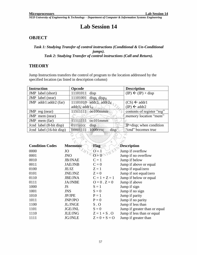
Microprocessors Lab Session 14 NED University of Engineering & Technology – Department of Computer & Information Systems Engineering
57
Lab Session 14
OBJECT
Task 1: Studying Transfer of control instructions (Conditional & Un-Conditional
jumps).
Task 2: Studying Transfer of control instructions (Call and Return).
THEORY
Jump Instructions transfers the control of program to the location addressed by the
specified location (as listed in description column)
Instruction Opcode Description
JMP label (short) 11101011 disp (IP) (IP) + disp
JMP label (near) 11101001 dispL dispH
JMP addr1:addr2 (far) 11101010 addr2L addr2H
addr1L addr1H
(CS) addr1
(IP) addr2
JMP reg (near) 11111111 oo100mmm contents of register “reg”
JMP mem (near) memory location “mem”
JMP mem (far) 11111111 oo101mmm
Jcnd label (8-bit disp) 0111cccc disp IP+disp; when condition
“cnd” becomes true Jcnd label (16-bit disp) 00001111 1000cccc disp
Condition Codes Mnemonic Flag Description
0000 JO O = 1 Jump if overflow
0001 JNO O = 0 Jump if no overflow
0010 JB/JNAE C = 1 Jump if below
0011 JAE/JNB C = 0 Jump if above or equal
0100 JE/JZ Z = 1 Jump if equal/zero
0101 JNE/JNZ Z = 0 Jump if not equal/zero
0110 JBE/JNA C = 1 + Z = 1 Jump if below or equal
0111 JA/JNBE O = 0 . Z = 0 Jump if above
1000 JS S = 1 Jump if sign
1001 JNS S = 0 Jump if no sign
1010 JP/JPE P = 1 Jump if parity
1011 JNP/JPO P = 0 Jump if no parity
1100 JL/JNGE S . O Jump if less than
1101 JGE/JNL S = 0 Jump if greater than or equal
1110 JLE/JNG Z = 1 + S . O Jump if less than or equal
1111 JG/JNLE Z = 0 + S = O Jump if greater than
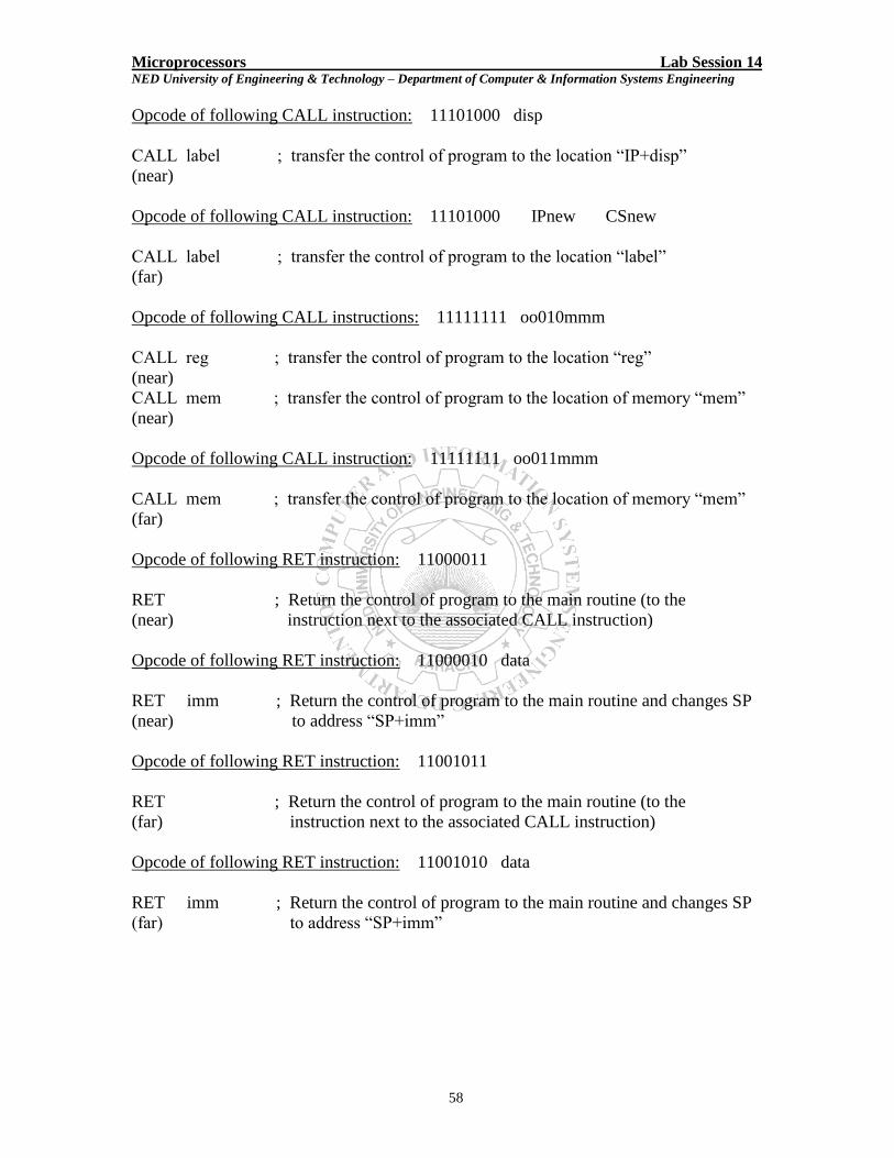
Microprocessors Lab Session 14 NED University of Engineering & Technology – Department of Computer & Information Systems Engineering
58
Opcode of following CALL instruction: 11101000 disp
CALL label ; transfer the control of program to the location “IP+disp”
(near)
Opcode of following CALL instruction: 11101000 IPnew CSnew
CALL label ; transfer the control of program to the location “label”
(far)
Opcode of following CALL instructions: 11111111 oo010mmm
CALL reg ; transfer the control of program to the location “reg”
(near)
CALL mem ; transfer the control of program to the location of memory “mem”
(near)
Opcode of following CALL instruction: 11111111 oo011mmm
CALL mem ; transfer the control of program to the location of memory “mem”
(far)
Opcode of following RET instruction: 11000011
RET ; Return the control of program to the main routine (to the
(near) instruction next to the associated CALL instruction)
Opcode of following RET instruction: 11000010 data
RET imm ; Return the control of program to the main routine and changes SP
(near) to address “SP+imm”
Opcode of following RET instruction: 11001011
RET ; Return the control of program to the main routine (to the
(far) instruction next to the associated CALL instruction)
Opcode of following RET instruction: 11001010 data
RET imm ; Return the control of program to the main routine and changes SP
(far) to address “SP+imm”

Microprocessors Lab Session 14 NED University of Engineering & Technology – Department of Computer & Information Systems Engineering
59
ASSEMBLER PROGRAM 1 INT 8 Console In (Input a character from the keyboard and store it into the AL reg.
INT B Console Out (Output a character contained in AL to the LCD.
JMP 0000 Jump to the first instruction.
OBSERVATIONS 1 By using single stepping observe the working of the program. Record the content of the
AX registers.
Character AX
1
2
3
4
5
ASSEMBLER PROGRAM 2 MOV AX, 0000
MOV BX, 0000
INT 8 ;Input from Keyboard
INT B ;Output the character
MOV BL, AL
INT 8 ;Input from Keyboard
INT B ;Output the character
CMP AX, BX ;Compare the values in AX and BX
JNZ 0000 ;if not equal jump to start of program.
INT 7
OBSERVATIONS 2 By using single stepping observe the contents of registers AX, BX after execution of each
instruction.
(Different Key input) (Same Key Input)
AX BX AX BX After 1
st instruction __________ __________ __________ __________
After 2nd
instruction __________ __________ __________ __________
After 3rd
instruction __________ __________ __________ __________
After 4th
instruction __________ __________ __________ __________
After 5th
instruction __________ __________ __________ __________
After 6th
instruction __________ __________ __________ __________
After 7th
instruction __________ __________ __________ __________
After 8th
instruction __________ __________ __________ __________
After 9th
instruction __________ __________ __________ __________
Flag register after
8th
instruction

Microprocessors Lab Session 14 NED University of Engineering & Technology – Department of Computer & Information Systems Engineering
60
ASSEMBLER PROGRAM 3
MOV AX , 5AD8
MOV CX , 0006
MOV WORD[FE], 349A
MOV WORD[100], 9CFF
MOV WORD[102], A9B6
MOV AX , WORD[102]
CALL LABEL
MOV CX , DX
JMP HERE
LABEL: PUSH AX
MOV AX , WORD[FE]
INC WORD[100]
ADD AX , WORD[100]
ROL AX , CL
XOR WORD[102] , AX
SBB WORD[FE] , AX
MOV DX , AX
POP AX
RET
HERE: CMP AX , CX
OBSERVATIONS 3 By using single stepping observe the contents of registers AX, BX, CX, DX and memory
location FE, 100 and 102.
Before Execution
AX : __________ ; BX : __________
CX : __________ ; DX : __________
SP : __________ ; WORD[FE] : __________
WORD[100] : __________ ; WORD[102] : __________
After CALL instruction
AX : __________ ; BX : __________
CX : __________ ; DX : __________
SP : __________ ; WORD[FE] : __________
WORD[100] : __________ ; WORD[102] : __________
After RET instruction
AX : __________ ; BX : __________
CX : __________ ; DX : __________
SP : __________ ; WORD[FE] : __________
WORD[100] : __________ ; WORD[102] : __________
Microprocessors Lab Session 14 NED University of Engineering & Technology – Department of Computer & Information Systems Engineering
61
After Execution
AX : __________ ; BX : __________
CX : __________ ; DX : __________
SP : __________ ; WORD[FE] : __________
WORD[100] : __________ ; WORD[102] : __________
EXERCISE 1
Write a program, which prints your name on the LCD display when ‘space’ key is
pressed from the keyboard. Implement using conditional jump instruction. Also draw the
flow chart of the program.
Program Flowchart
___________________________________
___________________________________
___________________________________
___________________________________
___________________________________
___________________________________
___________________________________
___________________________________
___________________________________
___________________________________
___________________________________
___________________________________
___________________________________
___________________________________
___________________________________
___________________________________
___________________________________
___________________________________
___________________________________
___________________________________
___________________________________
___________________________________
___________________________________
___________________________________
___________________________________
___________________________________
___________________________________
___________________________________
___________________________________
___________________________________
___________________________________
___________________________________

Microprocessors Lab Session 14 NED University of Engineering & Technology – Department of Computer & Information Systems Engineering
62
EXERCISE 2
Write a program, which takes input from port address 3060h then calls a subroutine
having label ‘ADDNOS’. ADDNOS subroutine adds the inputted values from the
specified input port. The program takes input from port 10 times. Produce a certain delay
by using a subroutine between two consecutive inputs from port. Program stores the final
result as a word on memory location 0200. Also draw the flow chart of the program.
Program Flowchart
___________________________________
___________________________________
___________________________________
___________________________________
___________________________________
___________________________________
___________________________________
___________________________________
___________________________________
___________________________________
___________________________________
___________________________________
___________________________________
___________________________________
___________________________________
___________________________________
___________________________________
___________________________________
___________________________________
___________________________________
___________________________________
___________________________________
___________________________________
___________________________________
___________________________________
___________________________________
___________________________________
___________________________________
___________________________________
___________________________________
___________________________________
___________________________________
___________________________________
Microprocessors Lab Session 15 NED University of Engineering & Technology – Department of Computer & Information Systems Engineering
63
Lab Session 15
OBJECT
Learning Isolated I/O instructions.
THEORY
IN acc , pt opcode = 1110010w port# ; Takes an 8-bit binary
number as input from input port “port#” and stores that in Accumulator.
IN acc , DX opcode = 1110110w ; Takes an 8-bit binary number as input from
input port addressed by DX and stores that in Accumulator.
OUT pt , acc opcode = 1110010w port# ; Outputs an 8-bit number from
Accumulator to output port number “port#”.
OUT DX , acc opcode = 1110111w ; Outputs an 8-bit number from Accumulator
to output port addressed by DX.
ASSEMBLER PROGRAM
INPUT PORT
MOV AX , 0
MOV DX , 1A3
IN AL , DX
INT 7
OUTPUT PORT
MOV AL , 41
MOV DX , 1A1
OUT DX , AL
INT 7
S. No. AL Character
1
2
3
4
5

Microprocessors Lab Session 15 NED University of Engineering & Technology – Department of Computer & Information Systems Engineering
64
EXERCISE
Write a program, which output the first ten numbers of Fibonacci series. You can also use
any assembler for this exercise. (Hint: Use looping technique, to output numbers one by
one in each iteration of loop)
Program Flowchart
__________________________________
__________________________________
__________________________________
__________________________________
__________________________________
__________________________________
__________________________________
__________________________________
__________________________________
__________________________________
__________________________________
__________________________________
__________________________________
__________________________________
__________________________________
__________________________________
__________________________________
__________________________________
__________________________________
__________________________________
__________________________________
__________________________________
__________________________________
__________________________________
__________________________________
__________________________________
__________________________________
__________________________________
__________________________________
__________________________________
__________________________________
__________________________________
__________________________________
__________________________________
__________________________________
__________________________________
__________________________________
Microprocessors Lab Session 16 NED University of Engineering & Technology – Department of Computer & Information Systems Engineering
65
Lab Session 16
OBJECT Using ADC/DAC
THEORY
Analog Interface
The MC8088 Analog interface provides one 8-bit ADC (0804) and one 8-bit DAC
(0800).
The port address of DAC and ADC is 10C h.
DIGITAL /ANALOG CONVERTER
The digital/analog converter uses an IC34 latch (74374) directly connected to the data
bus in order to give the digital information to the conversion device (DAC – 0800). The
current of the digital signal to be transmitted is converted into the corresponding voltage
signal with the operational IC36 (I – V converter)
ANALOG / DIGITAL CONVERTER
The analog / digital converter uses the ADC0804 for converting and a buffer (74244) for
data bus communication of the system.
DAC PROGRAMMING
This program outputs a value from 00h to FFh on the DAC port. Observe the analog
output of the program using a multi meter.
Program:
START:
MOV DX,10C ; Move address of DAC in DX
MOV AL,0 ; reset AL
LOOP: INT E ; Display AL in Hex Format
PUSH AX ; save AL on stack
INT 8 ; Wait for a keyboard hit
POP AX
OUT DX, AL ; OUT to DAC at 10C h
INC AL
JNZ LOOP ;if AL is not zero then repeat
INT 7 ; EXIT
Microprocessors Lab Session 16 NED University of Engineering & Technology – Department of Computer & Information Systems Engineering
66
ADC PROGRAMMING
Apply analogue voltage at the analogue input of ADC using variable power supply (0-
10V DC) and take the digital input from the ADC port at 10C h and display it on the
LCD.
Program:
START:
MOV DX, 10C ; Move address of ADC in DX
LOOP: INT 8 ; Wait for a keyboard hit
IN AL, DX ; IN from ADC at 10C h
INT E ; display AL on LCD in HEX format
JMP LOOP ; repeat
INT 7
OBSERVATION
DAC PROGRAMMING:
Observe the multimeter reading for the following values of AL register.
Value of AL register Multimeter Reading (Volts)
1) 00 ----------------
2) 15 ----------------
3) DE ----------------
4) FC ----------------
ADC PROGRAMMING:
Observe the value of AL register for following values of multimeter.
Multimeter Reading (Volts) Value of AL register
1) 1.5 ----------------
2) 3.8 ----------------
3) 6.3 ----------------
4) 9.8 ----------------

Microprocessors Lab Session 17 NED University of Engineering & Technology – Department of Computer & Information Systems Engineering
67
Lab Session 17
OBJECT
Interfacing Printer with 8088
THEORY
PARALLEL PRINTER INTERFACE
This section of the MC8088 trainer board offers 1 OUTPUT parallel port per printer.
The unit contains all the test points related to the MC8088 signals:
Address
Data
Control signals
It also contains an expansion connector on which the bus signals are reported.
This powers the system with external hardware.
The 25 pin connector complete pin-out is shown below:
STROBE 1 14 AUTOFD
D0 2 15 ERROR
D1 3 16 INIT
D2 4 17 SLCT IN
D3 5 18 GROUND
D4 6 19 GROUND
D5 7 20 GROUND
D6 8 21 GROUND
D7 9 22 GROUND
AK 10 23 GROUND
BUSY 11 24 GROUND
PE 12 25 GROUND
SLCT 13
The operation involving the parallel output is controlled by 8 data lines (D0 – D7) and the
two lines related to handshaking: BUSY and STROBE controls.
The data are sent to the printer with an IC47 buffer with 1E0H address.
The BUSY line is connected to line 6 of buffer IC7 (line 6 connected to relative bus data
line with weight 2^6=64) and is used as input.

Microprocessors Lab Session 17 NED University of Engineering & Technology – Department of Computer & Information Systems Engineering
68
The STROBE line is used toward the printer and goes from the system to the printer
buffer to inform the printer that the byte to be printed is available on the data lines. It is
connected to line 7 of buffer IC3 and to the data bus line with weight 2^7=128.
The timing diagram for the printing operation is:
BUSY
DATA
STROBE
The BUSY line coming from the printer must be at low logic level for a printing
operation; with high logic level the device is in printing state related to a former
character.
In a second time data to be printed must be introduced and buffer IC47 must be loaded
with byte related to the desired character or control.
At last the line STROBE must be put at low logic level for a moment (STROBE is ON
and low) to memorize bytes to be printed in the printer buffer.
ASSEMBLY PROGRAM
PARALLEL PRINTER PROGRAMMING
PRINTER PORT ADDRESSES
DATA 1E0 H
STROBE 180 H bit 7
BUSY 1C0 H bit 6
This program prints typed characters
0008 : 0000 INT 8 ;load typed character in AL

Microprocessors Lab Session 17 NED University of Engineering & Technology – Department of Computer & Information Systems Engineering
69
0002 PUSH AX
0003 MOV DX , 1C0 ;read BUSY port
0006 IN AL , DX
0007 TEST AL , 40 ;test bit 6 of byte read
0009 JNZ 3
00OB POP AX
00OC MOV DX , 1E0 ;send data to port 1E0h
00OF OUT DX , AL
0010 MOV DX , 180 ;generate strobe pulse
0013 IN AL , DX
0014 SUB AL, 80
0016 OUT DX , AL
0017 ADD AL , 80
0019 OUT DX , AL
001A JMP 00

Microprocessors Lab Session 18(a) NED University of Engineering & Technology – Department of Computer & Information Systems Engineering
70
Lab Session 18(a)
Series-Parallel Logic
OBJECT
To learn how to handle elements when connecting them in series (an AND circuit) or
in parallel (an OR circuit).
THEORY
Input I1 is ORed with input I2 and this Logical combination of element is ANDed with
input I3. Whether or not input I3 passes power flow to output element O1 depends on
whether input 11 or input 12 passes a current flow.
Suppose we try this new combination of AND and OR functions in Figur 2.
Microprocessors Lab Session 18(a) NED University of Engineering & Technology – Department of Computer & Information Systems Engineering
71
PROCEDURE
Program the PLC with this circuit:
1. To execute CX-programmer, do the following steps:
Click the START and go to All Programs.
Select the folder Omron then the folder CX-Programmer.
Click on CX-Programmer to start.
2. To start a new project, perform the following steps:
Step 1: Create a New Project
Select <File> -- <New> OR click on the New Project icon.
A project window will appear, with a <Change PLC> window.
Step 2: Select your Settings
Assign a name for the PLC at the Device Name (Default – NewPLC1).
Select the appropriate PLC model (CPM2* for this PLC) by clicking on Device Type.
Set the driver to the COM port (in Network Type Settings) connected from PC to
PLC.
After the setup has been done, the programming screens will appear. There are 4
different windows:
Ladder design window
Project work space
Output Window Error on Compiling
Watch window I/O Monitor
Ladder Design Window:
1. Develop the given ladder logic in Figure 1 in this window by following these
steps:
Place a new contact by clicking on it from toolbar and then clicking on ladder
design window at the desired location.
Write 0.00 in Edit contact and press OK then write I1 in Edit comment field and
press OK.
Place another new contact by clicking on it from toolbar and then clicking on
ladder design window at the right of I1.
Write 0.01 in Edit contact and press OK then write I2 in Edit comment field and
press OK.
Place a new coil by clicking on it from toolbar and then clicking on ladder design
window at the right of I2.

Microprocessors Lab Session 18(a) NED University of Engineering & Technology – Department of Computer & Information Systems Engineering
72
Write 10.00 in Edit contact and press OK then write O1 in Edit comment field and
press OK.
Place a vertical wire connection in between I1 and I2 for connecting I3 in parallel
of I1.
Place another new contact by clicking on it from toolbar and then clicking on
ladder design window at the bottom of I1.
Write 0.02 in Edit contact and press OK then write I3 in Edit comment field and
press OK.
2. Compile this program by clicking on Program Menu and by selecting Compile
option. Another window appears with number on errors and warning message.
3. Now change PLC mode to online from PLC menu and selecting Work online OR
by pressing Work On-line button from toolbar. A confirmation dialogue is
displayed, select the Yes pushbutton to connect.
4. Select the Download button from the toolbar. The Download Options dialogue is
displayed.
5. Set the Programs field and select the OK pushbutton.
6. Deselect the Work Online option. Now you can observe the operation of PLC on
the PC monitor.
TEST THE CIRCUIT
Output 10.00 should be energized when:
I-01 and I-02 are pressed.
or
I-03 and I-02 are pressed.
TASK
Develop the logic given in Figure 2 and test its operation:
Output:
___________________________________________________________________.
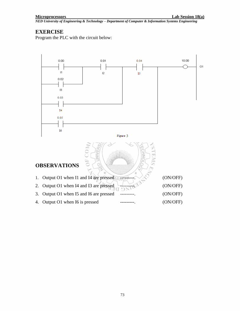
Microprocessors Lab Session 18(a) NED University of Engineering & Technology – Department of Computer & Information Systems Engineering
73
EXERCISE Program the PLC with the circuit below:
OBSERVATIONS
1. Output O1 when I1 and I4 are pressed ---------. (ON/OFF)
2. Output O1 when I4 and I3 are pressed ---------. (ON/OFF)
3. Output O1 when I5 and I6 are pressed ---------. (ON/OFF)
4. Output O1 when I6 is pressed ---------. (ON/OFF)
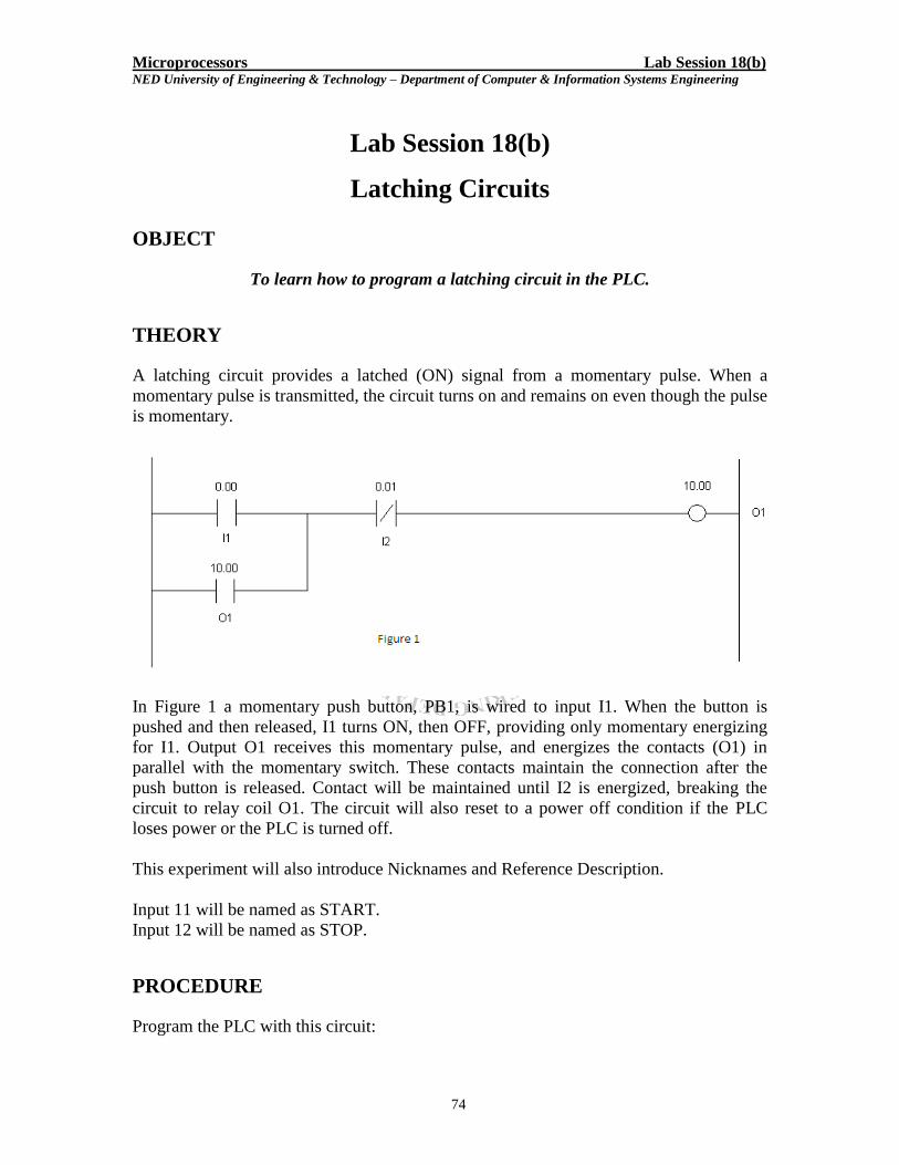
Microprocessors Lab Session 18(b) NED University of Engineering & Technology – Department of Computer & Information Systems Engineering
74
Lab Session 18(b)
Latching Circuits
OBJECT
To learn how to program a latching circuit in the PLC.
THEORY
A latching circuit provides a latched (ON) signal from a momentary pulse. When a
momentary pulse is transmitted, the circuit turns on and remains on even though the pulse
is momentary.
In Figure 1 a momentary push button, PB1, is wired to input I1. When the button is
pushed and then released, I1 turns ON, then OFF, providing only momentary energizing
for I1. Output O1 receives this momentary pulse, and energizes the contacts (O1) in
parallel with the momentary switch. These contacts maintain the connection after the
push button is released. Contact will be maintained until I2 is energized, breaking the
circuit to relay coil O1. The circuit will also reset to a power off condition if the PLC
loses power or the PLC is turned off.
This experiment will also introduce Nicknames and Reference Description.
Input 11 will be named as START.
Input 12 will be named as STOP.
PROCEDURE
Program the PLC with this circuit:
Microprocessors Lab Session 18(b) NED University of Engineering & Technology – Department of Computer & Information Systems Engineering
75
1. To execute CX-programmer, do the following steps:
Click the START and go to All Programs.
Select the folder Omron then the folder CX-Programmer.
Click on CX-Programmer to start.
2. To start a new project, perform the following steps:
Step 1: Create a New Project
Select <File> -- <New> OR click on the New Project icon.
A project window will appear, with a <Change PLC> window.
Step 2: Select your Settings
Assign a name for the PLC at the Device Name (Default – NewPLC1).
Select the appropriate PLC model (CPM2* for this PLC) by clicking on Device Type.
Set the driver to the COM port (in Network Type Settings) connected from PC to
PLC.
After the setup has been done, the programming screens will appear. There are 4
different windows:
Ladder design window
Project work space
Output Window Error on Compiling
Watch window I/O Monitor
Ladder Design Window:
1. Develop the given ladder logic in Figure 1 in this window by following these
steps:
Place a new contact by clicking on it from toolbar and then clicking on ladder
design window at the desired location.
Write 0.00 in Edit contact and press OK then write I1 in Edit comment field and
press OK.
Now Place a new closed contact by clicking on it from toolbar and then clicking
on ladder design window at the right of I1.
Write 0.01 in Edit contact and press OK then write I2 in Edit comment field and
press OK.
Place a new coil by clicking on it from toolbar and then clicking on ladder design
window at the right of I2.
Write 10.00 in Edit contact and press OK then write O1 in Edit comment field and
press OK.
Place a vertical wire connection in between I1 and I2 for connecting I3 in parallel
of I1.
Place another new contact by clicking on it from toolbar and then clicking on
ladder design window at the bottom of I1.
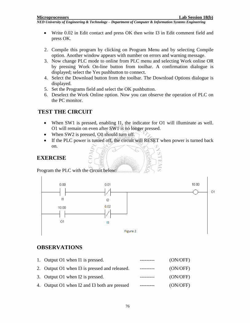
Microprocessors Lab Session 18(b) NED University of Engineering & Technology – Department of Computer & Information Systems Engineering
76
Write 0.02 in Edit contact and press OK then write I3 in Edit comment field and
press OK.
2. Compile this program by clicking on Program Menu and by selecting Compile
option. Another window appears with number on errors and warning message.
3. Now change PLC mode to online from PLC menu and selecting Work online OR
by pressing Work On-line button from toolbar. A confirmation dialogue is
displayed; select the Yes pushbutton to connect.
4. Select the Download button from the toolbar. The Download Options dialogue is
displayed.
5. Set the Programs field and select the OK pushbutton.
6. Deselect the Work Online option. Now you can observe the operation of PLC on
the PC monitor.
TEST THE CIRCUIT
When SW1 is pressed, enabling I1, the indicator for O1 will illuminate as well.
O1 will remain on even after SW1 is no longer pressed.
When SW2 is pressed, O1 should turn off.
If the PLC power is turned off, the circuit will RESET when power is turned back
on.
EXERCISE
Program the PLC with the circuit below:
OBSERVATIONS
1. Output O1 when I1 is pressed. --------- (ON/OFF)
2. Output O1 when I3 is pressed and released. --------- (ON/OFF)
3. Output O1 when I2 is pressed. --------- (ON/OFF)
4. Output O1 when I2 and I3 both are pressed --------- (ON/OFF)

Microprocessors Lab Session 18(c) NED University of Engineering & Technology – Department of Computer & Information Systems Engineering
77
Lab Session 18(c)
Timer Circuits
OBJECT
To learn how to program a Timer circuit in the PLC.
THEORY
The internal PLC timer consists of an enabling input, a reset input, and a timer preset
value.
The figure shows the basic timer function in a logic circuit.
This circuit delays power to O1 until a preset time has elapsed. The Set Value sets the
length of the time delay in multiple of 0.1 seconds. In the above figure, the constant value
of 40 will result in a 4 seconds time delay between the time I1 is energized and O1
output.
PROCEDURE
Program the PLC with this circuit:
1. To execute CX-programmer, do the following steps:

Microprocessors Lab Session 18(c) NED University of Engineering & Technology – Department of Computer & Information Systems Engineering
78
Click the START and go to All Programs.
Select the folder Omron then the folder CX-Programmer.
Click on CX-Programmer to start.
2. To start a new project, perform the following steps:
Step 1: Create a New Project
Select <File> -- <New> OR click on the New Project icon.
A project window will appear, with a <Change PLC> window.
Step 2: Select your Settings
Assign a name for the PLC at the Device Name (Default – NewPLC1).
Select the appropriate PLC model (CPM2* for this PLC) by clicking on Device Type.
Set the driver to the COM port (in Network Type Settings) connected from PC to
PLC.
After the setup has been done, the programming screens will appear. There are 4
different windows:
Ladder design window
Project work space
Output Window Error on Compiling
Watch window I/O Monitor
Ladder Design Window:
1. Develop the given ladder logic in Figure 1 in this window by following these
steps:
Place a new contact by clicking on it from toolbar and then clicking on ladder
design window at the desired location.
Write 0.00 in Edit contact and press OK then write I1 in Edit comment field and
press OK.
Now Place a new PLC instruction by clicking on it from toolbar and then clicking
on ladder design window at the right of I1.
Write TIM 001 #40 in Edit Instruction and press OK then write Timer1 in Edit
comment field and press OK.
Place another new contact by clicking on it from toolbar and then clicking on
ladder design window just below I1 in the next rung.
Write TIM001 in Edit contact and press OK then write Timer1 in Edit comment
field and press OK.
Place a new coil by clicking on it from toolbar and then clicking on ladder design
window at the right of Timer1.
Write 10.00 in Edit contact and press OK then write O1 in Edit comment field and
press OK.

Microprocessors Lab Session 18(c) NED University of Engineering & Technology – Department of Computer & Information Systems Engineering
79
2. Compile this program by clicking on Program Menu and by selecting Compile
option. Another window appears with number on errors and warning message.
3. Now change PLC mode to online from PLC menu and selecting Work online OR
by pressing Work On-line button from toolbar. A confirmation dialogue is
displayed; select the Yes pushbutton to connect.
4. Select the Download button from the toolbar. The Download Options dialogue is
displayed.
5. Set the Programs field and select the OK pushbutton.
6. Deselect the Work Online option. Now you can observe the operation of PLC on
the PC monitor.
TEST THE PROGRAM
Four seconds after I1 is closed O1 will be energized.
The timer status will be displayed in real time on the program screen in either
online or monitor modes. Observe the time value shown on the program screen. If
the time is running, a number will increment on the timer. This reflects the timer’s
internal count. After the set value has been reached, the timer stops to increment.
Releasing I1 will reset the timer value to zero.
EXERCISE
Q: Design Ladder logic program for Priority determination design (Early Player Buzzer
First).
OPERATION:
The game buzzer control requirement:
1. After the Host has finished with question.
2. The 3 players will press the switch in front of them to fight to be first to
answer the question.
3. The buzzer will sound for 10 sec after any one of the players has touched the
switch.
4. The light indicator in front of each player will light-up and only reset by the
Host switch.
I/O ASSIGNMENT:
Input Device Output Device
00000 PB1 01000 Buzzer
00001 PB2 01001 Player1 light
00002 PB3 01002 Player2 light
00003 RST (reset) 01003 Player3 light

Microprocessors Lab Session 18(c) NED University of Engineering & Technology – Department of Computer & Information Systems Engineering
80
LADDER LOGIC:

Microprocessors Lab Session 18(c) NED University of Engineering & Technology – Department of Computer & Information Systems Engineering
81
OBSERVATIONS
_____________________________________________________________
___________________________________________________________
_____________________________________________________________
____________________________________________________________
_____________________________________________________________
_____________________________________________________________
_____________________________________________________________
_____________________________________________________________
__________________________________________________________

Microprocessors Lab Session 18(d) NED University of Engineering & Technology – Department of Computer & Information Systems Engineering
82
Lab Session 18(d)
Counter Circuits
OBJECT
To learn how to program a counter circuit in the PLC.
THEORY The basic counter within the PLC consists of the input the counter function, the counter
reset input, and the counter preset. Each part of the counter performs a very specific
function. Each part of the counter performs a very specific function. The counter must
first be enabled before it can count events. To enable the counter, the reset element must
be open initially. If the reset element is open, then closing the count element causes the
accumulated value of a counter to increase by 1.For example, if the accumulated value of
a counter was 7, the value would increase to 8 with the closing of the count element.
The accumulated value increases by 1each time the count element goes from open to
close. If the count element remain in the close position, the accumulated value increases
by only 1.The count element must then be opened and again closed in order to increases
the value by a count of 1.When the accumulated value of a counter is equal to a PRESET
value, the counter energizes the output relay coil.
Any time the RESET element is closed, the counter is RESET regardless of whether or
not the count contact is close. If the counter is RESET, the accumulated value of the
counter is RESET, to 0000 and the counter output is de-energized. This causes the output
relay coil and its associated contacts to change back to their original status-the normally
closed contacts close. These conditions will remain as long as the RESET element is
close. When the RESET element is again opened, the counter is ready to begin counting
all over again.
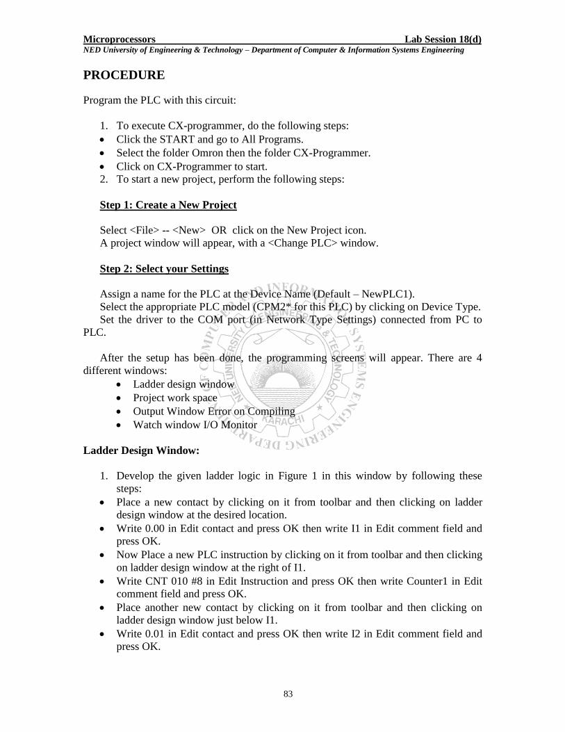
Microprocessors Lab Session 18(d) NED University of Engineering & Technology – Department of Computer & Information Systems Engineering
83
PROCEDURE
Program the PLC with this circuit:
1. To execute CX-programmer, do the following steps:
Click the START and go to All Programs.
Select the folder Omron then the folder CX-Programmer.
Click on CX-Programmer to start.
2. To start a new project, perform the following steps:
Step 1: Create a New Project
Select <File> -- <New> OR click on the New Project icon.
A project window will appear, with a <Change PLC> window.
Step 2: Select your Settings
Assign a name for the PLC at the Device Name (Default – NewPLC1).
Select the appropriate PLC model (CPM2* for this PLC) by clicking on Device Type.
Set the driver to the COM port (in Network Type Settings) connected from PC to
PLC.
After the setup has been done, the programming screens will appear. There are 4
different windows:
Ladder design window
Project work space
Output Window Error on Compiling
Watch window I/O Monitor
Ladder Design Window:
1. Develop the given ladder logic in Figure 1 in this window by following these
steps:
Place a new contact by clicking on it from toolbar and then clicking on ladder
design window at the desired location.
Write 0.00 in Edit contact and press OK then write I1 in Edit comment field and
press OK.
Now Place a new PLC instruction by clicking on it from toolbar and then clicking
on ladder design window at the right of I1.
Write CNT 010 #8 in Edit Instruction and press OK then write Counter1 in Edit
comment field and press OK.
Place another new contact by clicking on it from toolbar and then clicking on
ladder design window just below I1.
Write 0.01 in Edit contact and press OK then write I2 in Edit comment field and
press OK.

Microprocessors Lab Session 18(d) NED University of Engineering & Technology – Department of Computer & Information Systems Engineering
84
Place third new contact by clicking on it from toolbar and then clicking on ladder
design window just below I2 in the next rung.
Write CNT010 in Edit contact and press OK then write Counter1 in Edit comment
field and press OK.
Place a new coil by clicking on it from toolbar and then clicking on ladder design
window at the right of Counter1.
Write 10.00 in Edit contact and press OK then write O1 in Edit comment field and
press OK.
2. Compile this program by clicking on Program Menu and by selecting Compile
option. Another window appears with number on errors and warning message.
3. Now change PLC mode to online from PLC menu and selecting Work online OR
by pressing Work On-line button from toolbar. A confirmation dialogue is
displayed; select the Yes pushbutton to connect.
4. Select the Download button from the toolbar. The Download Options dialogue is
displayed.
5. Set the Programs field and select the OK pushbutton.
6. Deselect the Work Online option. Now you can observe the operation of PLC on
the PC monitor.
TEST THE PROGRAM
Press I1 eight times. The accumulated count will appear on the counter. At the
tenth switch closure O1 will energize.
Press I2 to reset the counter and repeat the experiment.
EXERCISE
Q: Design Ladder Logic Program for Packaging Line Control:
OPERATION: When PB1 (START Push Button) is pressed, the box conveyor moves. Upon detection of box
present, the box conveyor stops and the Apple conveyor starts. Part sensor will count for 10
apples. Apple conveyor stops and box conveyor starts again. Counter will be reset and
operation repeats until PB2 (STOP Push Button) is pressed.
I/O ASSIGNMENT:
Input Devices Output Devices
00000 START Push Button (PB1) 01000 Apple Conveyor
00001 STOP Push Button (PB2) 01001 Box Conveyor
00002 Part Present (SE1)
00003 Box Present (SE2)

Microprocessors Lab Session 18(d) NED University of Engineering & Technology – Department of Computer & Information Systems Engineering
85
LADDER LOGIC:
OBSERVATIONS
_____________________________________________________________
_____________________________________________________________
_____________________________________________________________
_____________________________________________________________
_____________________________________________________________
_____________________________________________________________
_____________________________________________________________
_____________________________________________________________
_____________________________________________________________
_____________________________________________________________
_____________________________________________________________

Microprocessors Lab Session 18(d) NED University of Engineering & Technology – Department of Computer & Information Systems Engineering
86
_____________________________________________________________
_____________________________________________________________
________________________________________________________ _____

87
CIRCUIT DIAGRAM
(Lab session 1-7)