micro/nano-electronics & vlsi activities in ee at iit …microel/pgs/micro_profile_2004.pdf ·...
TRANSCRIPT

1
Micro/Nano-electronics & VLSI activities in EE at IIT
Bombay
Department of Electrical EngineeringIndian Institute of Technology, Bombay
2004
IIT Bombay
• IIT Bombay is one of 7 IITs in India, and the oldest but one
• Located on a 250 hectare campus on the shores of Powai lake
• About 400 faculty and 5000 students• More than half of the students are post-
graduate students• 26 major Departments, Schools and Centres,
plus 6 inter-disciplinary programmes
2
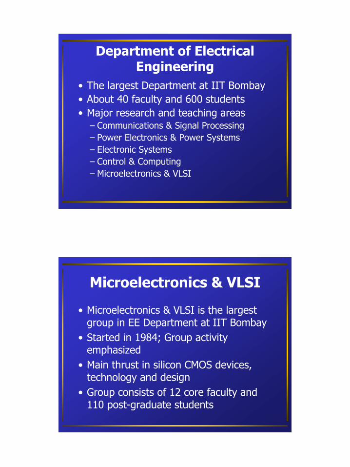
Department of Electrical Engineering
• The largest Department at IIT Bombay• About 40 faculty and 600 students• Major research and teaching areas
– Communications & Signal Processing– Power Electronics & Power Systems– Electronic Systems– Control & Computing– Microelectronics & VLSI
Microelectronics & VLSI
• Microelectronics & VLSI is the largest group in EE Department at IIT Bombay
• Started in 1984; Group activity emphasized
• Main thrust in silicon CMOS devices, technology and design
• Group consists of 12 core faculty and 110 post-graduate students
3
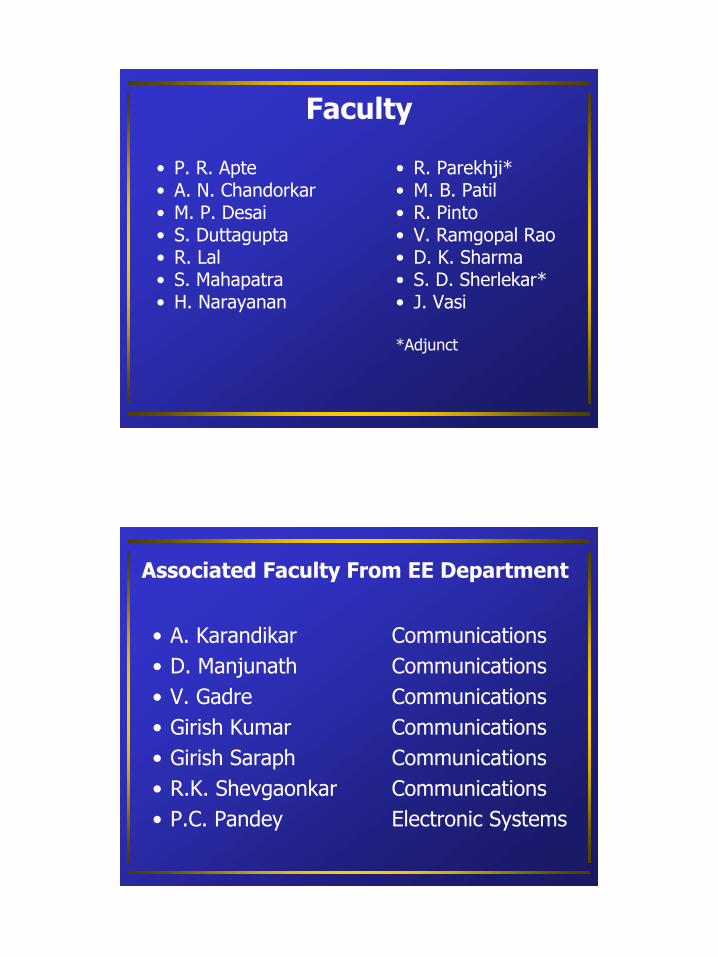
Faculty
• P. R. Apte• A. N. Chandorkar• M. P. Desai• S. Duttagupta• R. Lal• S. Mahapatra• H. Narayanan
• R. Parekhji* • M. B. Patil• R. Pinto• V. Ramgopal Rao• D. K. Sharma• S. D. Sherlekar*• J. Vasi
*Adjunct
Associated Faculty From EE Department
• A. Karandikar Communications• D. Manjunath Communications• V. Gadre Communications• Girish Kumar Communications• Girish Saraph Communications• R.K. Shevgaonkar Communications• P.C. Pandey Electronic Systems
4
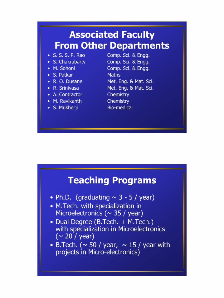
Associated FacultyFrom Other Departments
• S. S. S. P. Rao Comp. Sci. & Engg.• S. Chakrabarty Comp. Sci. & Engg.• M. Sohoni Comp. Sci. & Engg.• S. Patkar Maths• R. O. Dusane Met. Eng. & Mat. Sci.• R. Srinivasa Met. Eng. & Mat. Sci.• A. Contractor Chemistry• M. Ravikanth Chemistry• S. Mukherji Bio-medical
Teaching Programs
• Ph.D. (graduating ~ 3 - 5 / year)• M.Tech. with specialization in
Microelectronics (~ 35 / year)• Dual Degree (B.Tech. + M.Tech.)
with specialization in Microelectronics (~ 20 / year)
• B.Tech. (~ 50 / year, ~ 15 / year with projects in Micro-electronics)
5
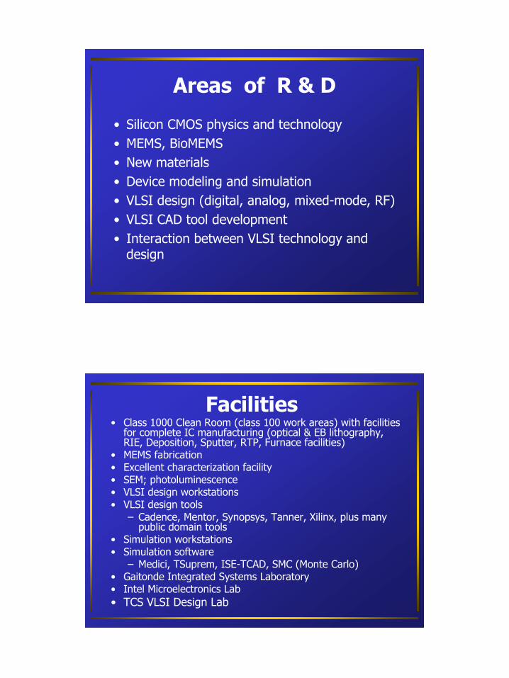
Areas of R & D
• Silicon CMOS physics and technology• MEMS, BioMEMS• New materials• Device modeling and simulation• VLSI design (digital, analog, mixed-mode, RF)• VLSI CAD tool development• Interaction between VLSI technology and
design
Facilities• Class 1000 Clean Room (class 100 work areas) with facilities
for complete IC manufacturing (optical & EB lithography, RIE, Deposition, Sputter, RTP, Furnace facilities)
• MEMS fabrication • Excellent characterization facility• SEM; photoluminescence• VLSI design workstations• VLSI design tools
– Cadence, Mentor, Synopsys, Tanner, Xilinx, plus many public domain tools
• Simulation workstations• Simulation software
– Medici, TSuprem, ISE-TCAD, SMC (Monte Carlo)• Gaitonde Integrated Systems Laboratory• Intel Microelectronics Lab• TCS VLSI Design Lab

6
Facilities: Clean Room
Facilities: Photolithography

7
Facilities: SEM/EBL
Facilities: Characterization

8
Facilities: Intel Lab
Facilities: TCS Lab

9
Facilities: TCS Lab
Sponsored Projects
• Over 60 projects since 1985 totaling US$ 8 Million
• Projects cover all areas of Microelectronics & VLSI
• Projects from major government agencies, and leading Indian & international companies

10
Some Recent & Ongoing Projects:Physics & Technology
• Silicon sensors for electroporation (PramanTechnology)
• iSens for cardiac applications (ADA)• Silicon Locket (TCS)• Channel engineering for 100 nm CMOS devices (DST)• Characterization of vertical MOS transistors with Sub
70 nm Channel Lengths (Siemens)• Design and characterization of Flash memories
(Hitachi)• Molecular Electronics- Porphyrin based (CDRG)• FinFET Circuit Simulations (IMEC)
Some Ongoing Projects:Modeling & Simulation
• Development of a hot-carrier simulator (Motorola)
• Look-up table modeling for circuit simulation (DST)
• Modeling of power semiconductor devices (GE)• Macromodels for circuit simulation (National)• RF MOSFET models (IME, Singapore)• Oxide scaling effects on design issues (Intel)• CMOS device design and optimization for mixed-
signal applications (Intel)
11
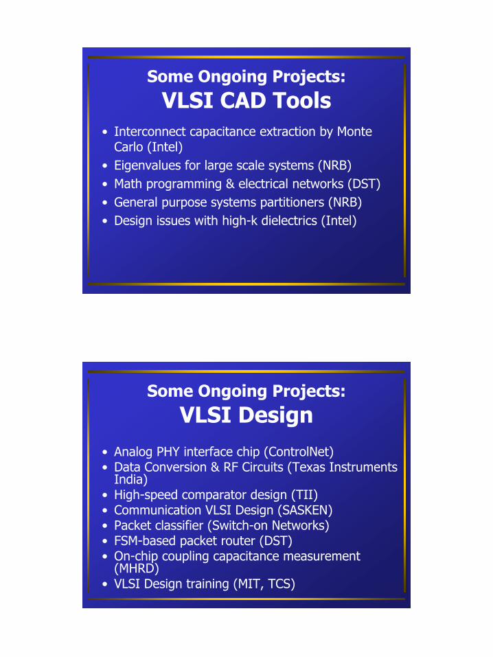
Some Ongoing Projects:VLSI CAD Tools
• Interconnect capacitance extraction by Monte Carlo (Intel)
• Eigenvalues for large scale systems (NRB)• Math programming & electrical networks (DST)• General purpose systems partitioners (NRB)• Design issues with high-k dielectrics (Intel)
Some Ongoing Projects:VLSI Design
• Analog PHY interface chip (ControlNet)• Data Conversion & RF Circuits (Texas Instruments
India)• High-speed comparator design (TII)• Communication VLSI Design (SASKEN)• Packet classifier (Switch-on Networks)• FSM-based packet router (DST)• On-chip coupling capacitance measurement
(MHRD) • VLSI Design training (MIT, TCS)

12
RF Design• Design of RF Tuner for Cable Modem Applications: V.Babu, S.
Seth and A.N. Chandorkar – won the best paper award at VLSI-2004
• A new Approach to Model Nonquasi-static (NQS) Effects For MOSFETS – A.S. Roy, J.M. Vasi and M.B. Patil, IEEE transactions on Electron Devices, ED-50, 2401 (2003)
• Dual Channel RF receiver design – A Krishnakanth, D. K. Sharma – 6th International Symposium on Wireless Multimedia communications WPMC ‘03, Yokosuka, Kanagawa, Japan, Dec 2003
• Linearization of RF Power Amplifiers – A. Kotwal, A.N. Chandorkar (M.Tech. Project)
• Power optimal RF data transfer for mobile heart monitoring –N. Nagaraju, S. Gupta, R. Lal, D.K. Sharma (3 M.Tech. Projects in progress)
Some Recent and Ongoing Ph. D. Theses
• S. Vaidya: Neutron radiation effects in MOS systems• J. Meckie: Asynchronous design issues• G. Trivedi: Parallel algorithms for VLSI optimization• N. Mahapatra: High-k dielectrics for 100 nm CMOS• A. Shastry: Microcapillary electrophoresis on silicon• C.A. Betty: Capacitive immunosensor on porous Si• B. Anand: Digital design with dynamic threshold CMOS• D. Nair: Flash memory design and reliability• D.V.Kumar: Look-up table approach for CMOS circuits• K. Narasimhulu: CMOS devices for mixed-signal
applications

13
Industry Collaborations• Sponsored, Consultancy & Collaborative Projects
– Indian industry: SCL, BEL, ITI, TCS, Sasken, TII, Cypress, ControlNet, National, etc
– International industry: Intel, Motorola, GE, Siemens, Hitachi, National, IME, Agere, IMEC
• Industry sponsorship of students– M.Tech. & Dual Degree students– Ph.D. students
• Endowed Laboratories– Gaitonde Integrated Systems Laboratory– Intel Microelectronics Laboratory– TCS VLSI Design & Characterization Laboratory
• Continuing Education Programs for industry
University Collaborations
• Research Collaborations – Other IITs, IISc, Universities of Bombay, Pune– International universities like
• UCLA, UCSB, Yale University (USA)• Hong Kong University of Science & Tech. (HK)• Delft University (The Netherlands)• University of Bundeswehr (Germany)• Griffith University (Australia)• NUS, NTU (Singapore)• IMEC (Belgium)
• Student Exchanges

14
Strengths
• Undertaken projects of national importance (over US $8 Million in the last 15 years) and successfully transferred technologies to industries
• Close industry interaction
• Excellent infrastructure
• High Visibility
1. Najeeb-ud-din, et.al., “Analysis of Floating Body Effects in Thin Film Conventional and Single Pocket SOI MOSFETs using the GIDL Current Technique”, IEEE Electron Device Letters, vol. 23, p. 209-211, April 2002
2. B. J. Daniel, et al., "Modeling of the CoolMOS transistor Part I: Device physics," IEEE Trans. Electron Devices, pp. 916-922, May 2002.
3. B. J. Daniel, et al., "Modeling of the CoolMOS transistor Part II: DC model and parameter extraction," IEEE Trans. Electron Devices, pp. 922-929, May 2002.
4. Nihar R. Mohapatra et.al., "The Effect of High-K Gate Dielectrics on Deep Sub-micrometer CMOS Device and Circuit Performance" IEEE Transactions on Electron Devices, vol.49, (no.5), May 2002, p.826-831
5. P.Sivaram et.al., “Silicon film thickness considerations in SOI-DTMOS”, IEEE Electron Device Letters, vol. 23, p. 276 –278, May 2002
6. D.G.Borse, et.al., , "Optimization and Realization of Sub 100nm Channel Length Single Halo p-MOSFETs" IEEE Transactions on Electron Devices, vol.49, (no.6), June 2002.
7. S. Mahapatra, et.al., “CHISEL Flash EEPROM. I. Performance and scaling” IEEE Transactions on Electron Devices, vol.49 p.1296 –1301, July 2002
8. S. Mahapatra, et.al., “CHISEL flash EEPROM. II. Reliability”, IEEE Transactions on Electron Devices, vol.49 p. 1302 -1307, July 2002
9. K.N.Manjularani, et al, "A New Method to Characterize Border Traps in Sub-Micron Transistors using Hysteresis in the Drain Current", IEEE Transactions on Electron Devices, vol. 50, No.4, pp. 973-979, 2003
10. Sahoo, D.K et al., “High-field effects in silicon nitride passivated GaN MODFETs “IEEE Transactions on Electron Devices, Volume: 50 Issue: 5 , May 2003, pp.1163 -1170
11. N.R.Mohapatra, et. al., "CHISEL programming Operation of Scaled NOR Flash EEPROMs-Effect of Voltage Scaling, Device Scaling, and Technological Parameters", IEEE Transactions on Electron Devices, vol. 50, No.2104-2111, October 2003
12. K.Narasimhulu et.al., "Impact of Lateral Asymmetric Channel Doping on Deep Sub-Micrometer Mixed-Signal Device and Circuit Performance", IEEE Transactions on Electron Devices vol. 50, pp.2481-2489, December 2003
Group’s publications in the area of Electron Devices in the last TWO Yearsin IEEE Trans. On Electron Devices/IEEE Electron Device Letters

15
13. Ananda Sankar Roy et al., “A New Approach to model non-quasi-static (NQS) effects for MOSFETs: Part I: Large Signal Analysis, IEEE Trans. Electron Devices, 51, (2004).
14. Ananda Sankar Roy et al., “A New Approach to model non-quasi-static (NQS) effects for MOSFETs: Part II:Small Signal Analysis, IEEE Trans. Electron Devices51, (2004).
15. B.Anand, et. al, "Silicon Film Thickness Optimization for SOI-DTMOS from Circuit Performance considerations", Accepted for publication, IEEE Electron Device Letters, June, 2004
16. K. Narasimhulu, et. al, , "The Effect of Lateral Asymmetric Channel (LAC) Doping on Deep Sub-micron Transistor Capacitances and its Influence on Device RF Performance", IEEE Trans. on Electron Devices, Sept. 2004
17. D. R. Nair, et. al, "Drain disturb during CHISEL programming of NOR Flash EEPROMs – Physical mechanisms and impact of technological parameters", IEEE Trans. Electron Devices, v.51, p.701, 2004
18. D. R. Nair, et. al, "Cycling endurance of NOR Flash EEPROM cells under CHISEL programming operation - Impact of technological parameters and scaling", accepted, to appear in IEEE Trans. Electron Devices, 2004
19. S. Mahapatra, et al.,, "Investigation and Modeling of Interface and Bulk Trap Generation During Negative Bias Temperature Instability of p-MOSFETs", IEEE Trans. Electron Devices, v.51, p.1371, 2004
20. P.Mali et al., “The DNA SET: a novel device for single-molecule DNA sequencing”IEEE Transactions on Electron Devices, Volume: 51 , Issue: 12 , Dec. 2004 Pages:2004 - 2012
The group had papers at IEDM 2002, IEDM 2003, IEDM 2004 IRPS 2003, IRPS 2004- the flagship Electron
Devices/Reliability conferences
Publications
• Over 200 publications in the last 5 years in major journals and conferences
• Cover all areas of interest• Details at www.ee.iitb.ac.in/ ~microel/

16
Conclusions
• Most active Micro/Nano-electronics & VLSI group in India
• Excellent research facilities• Close Industry Interaction• Major teaching programs at all
levels
Contacts• Microelectronics Group
Department of Electrical EngineeringIndian Institute of Technology, BombayPowaiMumbai 400076 India
• Phone: +91-22-2572-3655• Fax: +91-22-2572-3480• email: [email protected]• website: www.iitb.ac.in/~microel/