micromachining process simulation using a continuous cellular automata method
TRANSCRIPT

252 JOURNAL OF MICROELECTROMECHANICAL SYSTEMS, VOL. 9, NO. 2, JUNE 2000
Micromachining Process Simulation Using aContinuous Cellular Automata Method
Zhenjun Zhu and Chang Liu, Associate Member, IEEE
Abstract—In this paper, we present results on the developmentof an anisotropic crystalline etching simulation (ACES) programbased on a continuous cellular automata (CA) model. The programprovides improved spatial resolution and accuracy compared withthe conventional and stochastic CA methods. Implementationof a three-dimensional (3-D) dynamic CA technique providesincreased simulation speed and reduced memory requirement.The first ACES software based on common personal computerplatforms has been realized for simulation of micromachiningprocesses and visualizing results in 3-D space. The software isuniquely capable of simulating the resultant profile following aseries of micromachining steps, including surface passivation,reactive ion etching, as well as wet chemical bulk etching. Anovel method for accurately obtaining the etch-rate diagramof anisotropic etching using both experimental and numericaltechniques has been developed. [481]
Index Terms—Anisotropic etching, cellular automata methods,continuous cellular automata, etching simulation.
I. INTRODUCTION
A. Anisotropic Etching
A NISOTROPIC etching [1] of silicon is a prevalenttechnique for realizing three-dimensional (3-D) micro-
electromechanical system (MEMS) structures [2], [3]. Theprocess has been used for numerous application domains, in-cluding sensors (e.g., cavities of pressure sensors [3] and probesof scanning probe microscopes [4]), communications (e.g.,micromachined antennas [5]), and biomedical engineering(e.g., neuron wells [6]), to name only a few. The etching can beaccomplished using several chemical etchants, including ethy-lene–diamine pycocatechol (EDP) and potassium hydroxide(KOH). 3-D profiles resulting after timed etch are determinedboth by the 3-D etch-rate distribution and by initial conditions,including mask patterns and the initial 3-D profile of the sub-strate. Today, the anisotropic etching is increasingly being usedin conjunction with other process steps, such as reactive ionetching (RIE), to create even more sophisticated 3-D structures(two such applications are discussed in Section VI). As MEMSdesign and fabrication become increasingly advanced, efficientand accurate anisotropic etching simulation has gained criticalimportance [7], [8].
Manuscript received August 4, 1999; revised January 4, 2000. This work wassupported by Defence Advanced Research Projects Agency Composite CADProgram under Contract F30602-97-2-0328. Subject Editor, S. D. Senturia.
Z. Zhu is with the Micro Actuators, Sensors, and Systems Group, Universityof Illinois at Urbana-Champaign, Urbana, IL 61801 USA.
C. Liu is with the Microelectronics Laboratory, University of Illinois at Ur-bana-Champaign, Urbana, IL 61801 USA (e-mail: [email protected]).
Publisher Item Identifier S 1057-7157(00)04857-5.
Fig. 1. Schematic diagram of a diamond crystal lattice.
B. Etching Simulation
Models for simulating the anisotropic etching process gener-ally fall into two categories: the geometric models and cellularautomata (CA) models.
1) Geometrical Models:In a geometric model, the resul-tant 3-D shape after an elapsed period of etching is determinedby geometric rules [9]–[12] with the semiconductor substrateconsidered as a continuous entity. The Wulff–Jaccodine model[13]–[16], for instance, uses plane waves that propagate at a ratedetermined by the etch-rate diagram. A number of simulationprograms [17], [18] based on geometric models have been re-ported. One major disadvantage of the geometric model, how-ever, lies in the fact that it does not efficiently process complexstructures with merging features.
2) CA Models: The main advantage of CA models is thatthey exhibit high efficiency and accuracy when handling arbi-trarily complex mask shapes and merging of 3-D structures. Inthe CA method, a substrate is represented by an array of dis-crete cells that reside in a crystalline lattice (Fig. 1). Etchingof the substrate material is represented by removal of individualatoms according to etching rules. During etching, the decision toremove or retain a particular cell is based on the link status of itslattice neighbors according to cell-removal rules. The link statusis categorized by the number of neighboring cells and their rela-tive positions, with each possible case (Table I) associated witha specific strength of chemical bonds. Several reported simula-tion programs [19]–[24] have been implemented based on theCA method; the authors have reported earlier work on the con-tinuous CA algorithm [25]. It should be noted, however, thatCA methods face inherent challenges in several areas, includingthe computational costs. For example, letbe the cell size, thecomputation cost scales by the inverse of in conventionalCA methods, or at least by the inverse of using the dynamicCA algorithm (described in Section III). However, increase ofthe speed and reduction of the cost of computers today partiallyoffset this difficulty. Another challenge lies in the creation ofaccurate rules and parameters for new processes and substratematerials.
Conventional simple CA models (Table I) utilize discrete cellstates: a cell within a lattice can only assert one of two states:
1057–7157/00$10.00 © 2000 IEEE

ZHU AND LIU: MICROMACHINING PROCESS SIMULATION 253
TABLE ICONVENTIONAL CA RULES
“removed” or “retained.” Consequently, only discrete etch-rateratios along certain crystal axes (e.g., major crystal axes in-cluding and ) are allowed. The default ratio ofetch rates (for silicon) in three major axes, i.e., , , and
, are . Obviously, a conventional CA model over-simplifies the physical etching process and is not adequately ac-curate.
Subsequently, more comprehensive models have beendeveloped to increase the accuracy of CA simulation. Onesuch method, the stochastic CA method, is described in thisparagraph, while another, the continuous CA method, is intro-duced in Section II. Thanet al. first developed a CA algorithmwith a stochastic component [19] to account for realistic etchrates in different crystal planes. In it, the probability of a cellbeing removed during a certain etch step is not only determinedby the neighbor link status, but also by an assigned randomnumber . At every etch step and for each cell, the value ofassigned will be compared with a prescribed threshold value
, which corresponds to the relative etch rate in a particularlattice axis. If is greater than , a cell will be removed; elseit will be retained within the lattice. Although the stochastic CAmodel can handle arbitrary etch-rate ratios among major axes,it can sometimes lead to roughened surfaces due to randomizedcell removal from an atomically smooth crystal plane. Finishedsurfaces could be roughened, making it difficult to define edgesand planes as well as visually render simulation results.
II. CONTINUOUS CA MODEL
A second method that is capable of increasing the resolu-tion and accuracy of micromachining process simulation is aso-called continuous CA method [25]. Compared with the sto-chastic CA model, the new continuous CA model allows arbi-trary etch-rate ratios among major axes, but avoids generatingartificially roughened surfaces and, therefore, causes no loss ofresolution and accuracy. As a fundamental difference betweenthis and other existing CA models (conventional or stochastic),each cell in the system can havenondiscrete state variables,
with their values ranging continuously from 0 to 1. One conve-nient nondiscrete state of a cell is its mass (denoted). A cellcan assume arbitrary states between (“removed”) and
(“unetched”), corresponding to its extent of removal.The continuous CA method for anisotropic etching simula-
tion has been first reported in [21] to realize a robust CA modelthat predicts 3-D shape for arbitrary etchants and etch rates. Themodel assumes that a proper percentage of a cell in a tempo-rary array, as opposed to the entire cell, is removed upon eachetching step. An extended two-dimensional (2-D) algorithm isused to predict 3-D etching shapes. This method uses a stackof 2-D cell arrays. Once the topmost array has been calculatedfor a particular time, it is used to calculate the next lower array,and so on. This produces accurate 3-D predictions, but only forspecialized cases. A true 3-D algorithm, believed to be suitedfor general purposes, was reported to have been developed [21],but eventually not selected because of the significant barrier ofcomputational costs.
The computational speed of computers has increased by or-ders of magnitude in recent years as the price of computers andmemories dropped. A 3-D continuous CA algorithm is, there-fore, more realistic now in terms of computational cost. In thispaper, we have developed a continuous CA method based ongeneral 3-D cases. Arbitrary etch rates are incorporated usingnew nondiscrete state designation. During every etch step (withan associated time), the mass of a cell (ranging from 0 to 1)will be reduced by an amount that corresponds to the etch rateof the host surface. Cell removal rules based on nondiscrete cellstates are described in the following. Assuming that the desiredetch rate on a particular crystal plane is , and theelapsed time of each etch step is(with the default value beingone), the number of etch steps that are required to com-pletely remove a cell equals1
(1)
1A = dBe means thatA is the smallest integer that is greater thanB.
254 JOURNAL OF MICROELECTROMECHANICAL SYSTEMS, VOL. 9, NO. 2, JUNE 2000
Fig. 2. Simulation process (a) without and (b) with time compensation.
If is an exact multiple of , the effective etch rate of asurface, denoted , is equal to the desired etch rate
(2)
In cases where is not a multiple of , however, the valueof the effective etch rate would differ from that of the target etchrate, namely,
(3)
Under such commonly circumstances, independent removal ofa single cell is not possible because the mass of more than oneneighboring cell must besimultaneouslyadjusted during the laststep of the cell removal. The mismatch is illustrated inFig. 2(a). However, a cell-removal algorithm that involves mul-tiple cells is not desirable because the required memory willdouble.A cell-removal rule based on concurrent active cells atthe interface of the silicon material and the etching solutions ispreferred.
In order to achieve this goal, we have introduced a time-com-pensation method. When a cell is removed during an etch-step
, the etching of the next cell will not begin immediately untilthe next etch-step . The time balance of the etch-step
will be compensated in step for the etching of the nextcell [see Fig. 2(b)]. Thus, the time of a specific etch-step,is not always equal to ; rather, based on the -value of a cellin step , the compensation can be computed by the fol-lowing equations:
Initial conditions: (4)
If , then
(5)
(6)
(7)
otherwise
(8)
(9)
(10)
The introduction of time compensation results infor any etch-step . If the current active cell is to
be removed in an etch-step, (10) will be used to compute the
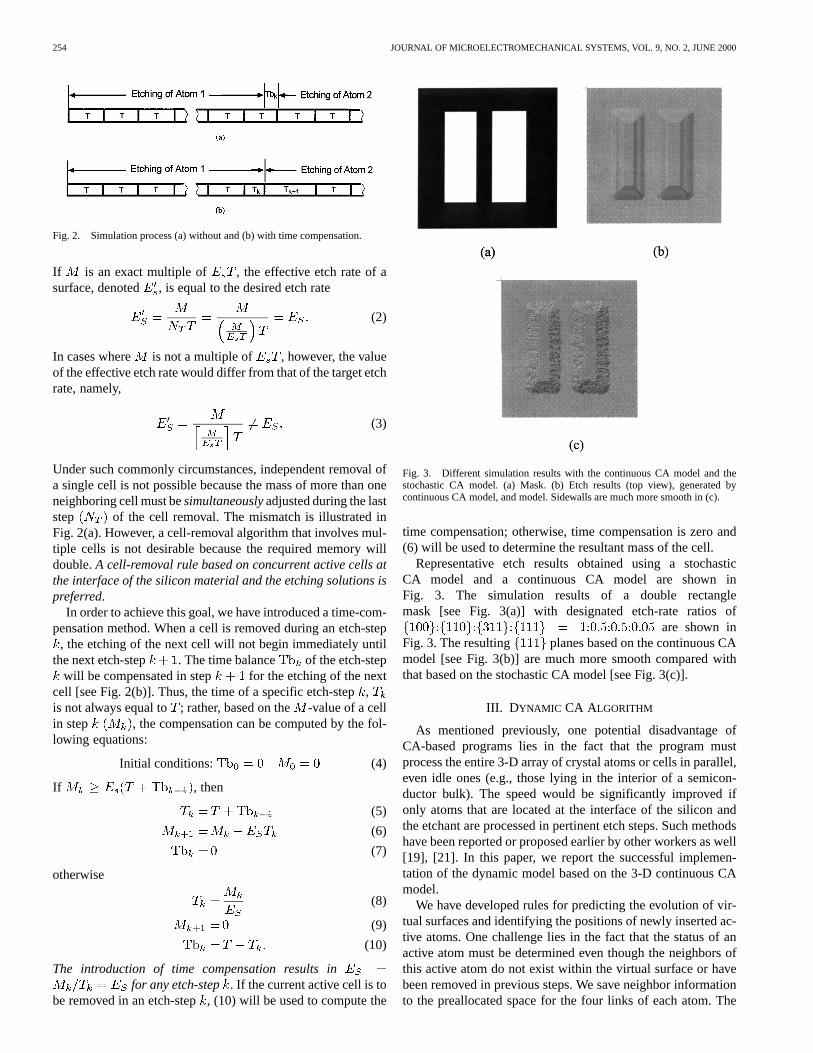
Fig. 3. Different simulation results with the continuous CA model and thestochastic CA model. (a) Mask. (b) Etch results (top view), generated bycontinuous CA model, and model. Sidewalls are much more smooth in (c).
time compensation; otherwise, time compensation is zero and(6) will be used to determine the resultant mass of the cell.
Representative etch results obtained using a stochasticCA model and a continuous CA model are shown inFig. 3. The simulation results of a double rectanglemask [see Fig. 3(a)] with designated etch-rate ratios of
are shown inFig. 3. The resulting planes based on the continuous CAmodel [see Fig. 3(b)] are much more smooth compared withthat based on the stochastic CA model [see Fig. 3(c)].
III. D YNAMIC CA ALGORITHM
As mentioned previously, one potential disadvantage ofCA-based programs lies in the fact that the program mustprocess the entire 3-D array of crystal atoms or cells in parallel,even idle ones (e.g., those lying in the interior of a semicon-ductor bulk). The speed would be significantly improved ifonly atoms that are located at the interface of the silicon andthe etchant are processed in pertinent etch steps. Such methodshave been reported or proposed earlier by other workers as well[19], [21]. In this paper, we report the successful implemen-tation of the dynamic model based on the 3-D continuous CAmodel.
We have developed rules for predicting the evolution of vir-tual surfaces and identifying the positions of newly inserted ac-tive atoms. One challenge lies in the fact that the status of anactive atom must be determined even though the neighbors ofthis active atom do not exist within the virtual surface or havebeen removed in previous steps. We save neighbor informationto the preallocated space for the four links of each atom. The

ZHU AND LIU: MICROMACHINING PROCESS SIMULATION 255
Fig. 4. Top views of models in different orientations. Black and white spheres represent atoms with different link-set types.
spatial coordinates of atoms are based on the lattice structureof silicon. For the diamond crystal lattice of silicon (Fig. 1),relevant properties of the lattice are as follows. First, there aretwo and only two types of atoms with different link-set types.Secondly, atoms with different link-set types (color coded asblack or white in subsequent diagrams) are interconnected. Allthe neighbors of an atom with link-set type I are in link-set typeII or vice versa. Based on these properties, rules for the evolu-tion of virtual surfaces have been developed for the first time[25]. Three rules, i.e., (E1)–(E3), are summarized as follows.(E1) A virtual surface is started in a horizontal plane. Active
atoms’ locations and link-set types are set based on theorientation of the lattice.
(E2) When an active atom ( ) is to be etched away basedon CA rules, its neighbors will be added to the virtualsurface if they are not in the surface. Positions of neigh-boring cells are calculated from ’s position and itslink-set types.
(E3) A newly added active atom’s link-set type is the oppositeof that of its neighbors.
Rules (E1) and (E2) are both related to the lattice’s orien-tation, including its top-surface orientation and edge alignment.
We have developed models for different orientations (Fig. 4), in-cluding wafers with surface orientation , , or .
The dynamic CA methods have indeed enabled greater simu-lation speeds, allowing the simulation program to run efficientlyon common personal computer platforms instead of dedicatedworkstations. A etch simulation with a 300 300 mask areacould proceed at the speed of 1 s per simulation step on a Pen-tium Pro 200 central processing unit (CPU). The memory re-quirement is significantly reduced as well. For instance, the re-quired memory under the dynamic method is merely 2 Mbytefor a 200 200 120 lattice, while the requirement under thestatic CA method is approximately 10 Mbyte.
IV. PROGRAM IMPLEMENTATION
Using the continuous CA model and dynamic method, wehave developed a micromachining process simulator, calledanisotropic crystalline etch simulation (ACES). It can simulatesilicon etching with different front-surface orientations invarious etchants, which exhibit different etch-rate ratios undervarying process parameters such as temperatures and concen-trations. The program receives 2-D mask designs in common

256 JOURNAL OF MICROELECTROMECHANICAL SYSTEMS, VOL. 9, NO. 2, JUNE 2000
Fig. 5. Comparison of rendering techniques. (a) Mask. (b) Depth-dependent rendering top view. (c) Depth-dependent rendering 3-D view. (d)Surface-normal-dependent rendering top view. (e) Surface-normal-dependent rendering 3-D view.
graphic formats (including CIF, GDSII, GIF, and BMP),generates 3-D profiles in standard solid-modeling formats, anddisplays results in integrated viewers based on OpenGL orVRML. The entire software can be run on a personal computerwithout resorting to external codes.
A. Visualization
Visualization of an etching result is realized by assigning spe-cific colors to atoms depending on specific depth within the 3-Dstructure or by the orientation of the surfaces in which the atomsare located. For this purpose, we have generated rules for map-ping the atom link status to the exact surface normal of the atomfor different wafer orientations [25]. Visualization results usingtwo different rendering techniques are shown in Fig. 5.
B. Surface Reconstruction and Edge Identification
Triangular meshes of etched 3-D geometry are required forpost processes, including finite-element analysis. Surface re-construction involves converting a simulation result from atomrepresentation to mesh representation. A number of methods
are available in the computer graphics literature [26], [27], butnone of them is well fitted for this case. We have developed anedge detectionmethod [26]–[29] to perform the conversion ef-ficiently, although there might be problems with small features.The method consists of the following three steps.Step 1) Plane identification: For all atoms in the entire vir-
tual surface , and scanning in a fixed order:
• locate the next unallocated atom suchthat it has more than three neighbors in the sameorientation;
• based on the atom’s position and orientation,generate a new polygon object and com-pute its plane equation;
• starting from , expand and mark atomsthat have the same orientation and also fit theplane equation. Save all visited atoms in .
Step 2) Neighbor identification:For all polygons generatedin step 1:
• for all atoms in polygon , find its neighboratom that belongs to another polygon ,mark and as neighbor.

ZHU AND LIU: MICROMACHINING PROCESS SIMULATION 257
Fig. 6. Example of the edge detection method. (a) Mask shape. (b) 3-D viewof the simulation result in atom model. (c) 3-D view of the simulation result inedge model.
Step 3) Edge computation:For all polygons:
• locate the next polygon that intersect withthree other polygons , , and .Generate a new edge object and com-pute one end point of from the intersec-tion of , , and . Compute theother end point of from the intersectionof , , and .
The edge detection method works especially well when thevirtual surface of a simulation result mainly contains all themajor planes in silicon lattice. Fig. 6 shows an example of edgedetection.
V. TEST AND VALIDATION
A. Results Verification of Anisotropic Etching
We have applied the ACES program to simulate the forma-tion of silicon tips using a square mask with the edges alignedin the direction. The tip is formed by etching -ori-ented surfaces vertically using the EDP solution. The simulationresults [see Fig. 7(a)] are well matched with experiments [seeFig. 7(b)]. A second test pattern contains circles with differentdiameters. The matched simulation and experimental results areshown in Fig. 8.
B. Etch-Rate Diagram Verification
The spoke pattern is commonly used to visualize theetch-rate diagram. Fig. 9(a) is a simulation result of spokepattern etching. It matches well with the experimental result[11], shown in Fig. 9(b). However, the spoke pattern methoddoes not yield sufficiently precise etch-rate values because theresolution of the physical mask is limited.
Fig. 7. Comparison of simulation and experimental results for ananisotropically etched tip array. (a) Simulation result. (b) Experimental result.The etch-rate ratio isf100g:f110g:f111g= 1:0:13:0.
Fig. 8. Comparison of simulation and etching results using a set of circles indifferent diameters. (a) Simulation. (b) Experiments. The dark circles in (a) andlight circles in (b) represent original mask shapes.
We have developed a new methodology for obtaining theetch-rate diagram with high angular resolution. The maskcontains a set of rectangular holes, each being 80-m longand 10- m wide, with 1 increments in angular positions[see Fig. 10(a)]. Etching for a relatively short period of time(5–10 min), the profile of the undercut cavity is parallel with thelong edge of the rectangle. Therefore, the etch rate associated

258 JOURNAL OF MICROELECTROMECHANICAL SYSTEMS, VOL. 9, NO. 2, JUNE 2000
Fig. 9. Comparison of simulation and etching results using a spoke pattern.(a) Simulation result. (b) Experimental result.
Fig. 10. Etching experiment and simulation for EDP etch-rate diagram. (a)Mask containing rotating rectangles with 1angle interval. (b) Etching resultof the whole pattern in EDP solution. (c) Etching result of a single rotatedrectangle in EDP solution. (d) Rotated rectangle mask for etching simulation.(e) Simulation result.
Fig. 11. Calibrated etch-rate diagram when the substrate front surface isf1 0 0g. (a) Etch-rate diagram from simulation. (b) Etch-rate diagram fromexperiment with etchant EDP. The angular resolution is 1�.
with a particular orientation can be obtained by measuringthe amount of lateral undercuts along the long edges [seeFig. 10(b)].
The procedure for characterizing the etch-rate diagram forsilicon orientation is shown. A single rectangle [see
Figs. 10(c)–(e)] has been magnified to show the match of the3-D shapes. The simulation result [see Fig. 11(a)] agrees wellwith the experimentally obtained etch diagram [see Fig. 11(b)],although a difference in details still exist because high-indexplanes are not implemented in the CA model.
VI. M ULTISTEPMICROMACHINING PROCESSSIMULATION
The capabilities of the ACES software have been recently ex-tended beyond simulating anisotropic etching alone. New pro-cesses are included, such as surface passivation (by thin-filmdeposition), diffusion doping of etch-stop layers, and the dryRIE. Currently, the ACES program is able to simulate and vi-sualize the result of a complete process flow involving severalsuccessive process steps. In the future, we plan to include moreprocesses with an increasing degree of fidelity based on the ex-isting framework in the future. The ability to simulate and visu-alize complex 3-D micromachining processes is believed to beimportant for both experts and new MEMS developers.
In anisotropic etching simulation, only two possible ma-terial interfaces for the dynamic atom set exist. They are theetchant-to-silicon and the mask-to-silicon interfaces. Atomsinterfacing with the mask are considered passivated and not
ZHU AND LIU: MICROMACHINING PROCESS SIMULATION 259
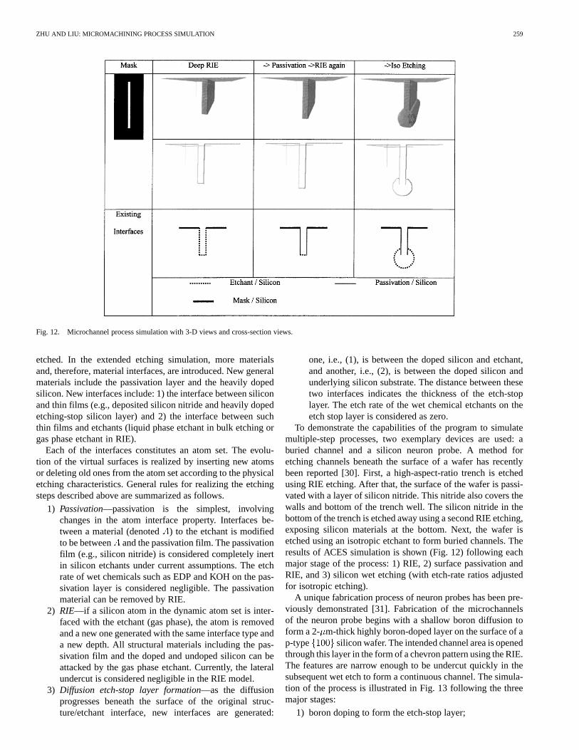
Fig. 12. Microchannel process simulation with 3-D views and cross-section views.
etched. In the extended etching simulation, more materialsand, therefore, material interfaces, are introduced. New generalmaterials include the passivation layer and the heavily dopedsilicon. New interfaces include: 1) the interface between siliconand thin films (e.g., deposited silicon nitride and heavily dopedetching-stop silicon layer) and 2) the interface between suchthin films and etchants (liquid phase etchant in bulk etching orgas phase etchant in RIE).
Each of the interfaces constitutes an atom set. The evolu-tion of the virtual surfaces is realized by inserting new atomsor deleting old ones from the atom set according to the physicaletching characteristics. General rules for realizing the etchingsteps described above are summarized as follows.
1) Passivation—passivation is the simplest, involvingchanges in the atom interface property. Interfaces be-tween a material (denoted) to the etchant is modifiedto be between and the passivation film. The passivationfilm (e.g., silicon nitride) is considered completely inertin silicon etchants under current assumptions. The etchrate of wet chemicals such as EDP and KOH on the pas-sivation layer is considered negligible. The passivationmaterial can be removed by RIE.
2) RIE—if a silicon atom in the dynamic atom set is inter-faced with the etchant (gas phase), the atom is removedand a new one generated with the same interface type anda new depth. All structural materials including the pas-sivation film and the doped and undoped silicon can beattacked by the gas phase etchant. Currently, the lateralundercut is considered negligible in the RIE model.
3) Diffusion etch-stop layer formation—as the diffusionprogresses beneath the surface of the original struc-ture/etchant interface, new interfaces are generated:
one, i.e., (1), is between the doped silicon and etchant,and another, i.e., (2), is between the doped silicon andunderlying silicon substrate. The distance between thesetwo interfaces indicates the thickness of the etch-stoplayer. The etch rate of the wet chemical etchants on theetch stop layer is considered as zero.
To demonstrate the capabilities of the program to simulatemultiple-step processes, two exemplary devices are used: aburied channel and a silicon neuron probe. A method foretching channels beneath the surface of a wafer has recentlybeen reported [30]. First, a high-aspect-ratio trench is etchedusing RIE etching. After that, the surface of the wafer is passi-vated with a layer of silicon nitride. This nitride also covers thewalls and bottom of the trench well. The silicon nitride in thebottom of the trench is etched away using a second RIE etching,exposing silicon materials at the bottom. Next, the wafer isetched using an isotropic etchant to form buried channels. Theresults of ACES simulation is shown (Fig. 12) following eachmajor stage of the process: 1) RIE, 2) surface passivation andRIE, and 3) silicon wet etching (with etch-rate ratios adjustedfor isotropic etching).
A unique fabrication process of neuron probes has been pre-viously demonstrated [31]. Fabrication of the microchannelsof the neuron probe begins with a shallow boron diffusion toform a 2- m-thick highly boron-doped layer on the surface of ap-type silicon wafer. The intended channel area is openedthrough this layer in the form of a chevron pattern using the RIE.The features are narrow enough to be undercut quickly in thesubsequent wet etch to form a continuous channel. The simula-tion of the process is illustrated in Fig. 13 following the threemajor stages:
1) boron doping to form the etch-stop layer;

260 JOURNAL OF MICROELECTROMECHANICAL SYSTEMS, VOL. 9, NO. 2, JUNE 2000
Fig. 13. Neuron probe process simulation with 3-D views and cross-section views.
2) RIE to expose the silicon;3) anisotropic silicon etch.
VII. CONCLUSION
Anisotropic etching of silicon is a key technique for realizing3-D MEMS structures. As MEMS design and fabricationbecome increasingly sophisticated, efficient and accurateanisotropic etching simulation becomes more important. Wepresent an ACES program based on a novel continuous CAmodel and a dynamic method. The continuous CA modelgreatly extended the capability of the CA model, enablinghigh accuracy and high efficiency of simulation. The dynamicCA technique resulted in increased simulation speed andreduced memory requirements. Experiments have validated thecontinuous CA model and the dynamic method. A new methodfor obtaining the etch-rate diagram has been demonstrated foraccurate generation of the etch-rate diagram.
REFERENCES
[1] K. E. Bean, “Anisotropic etching of silicon,”IEEE Trans. Electron De-vices, vol. ED-25, pp. 1178–1185, Oct. 1978.
[2] M. Madou,Fundamentals of Microfabrication. Boca Raton, FL: CRCPress, 1997.
[3] K. E. Petersen, “Silicon as a mechanical material,”Proc. IEEE, vol. 70,pp. 420–457, May 1982.
[4] C. Liu and R. Gamble, “Mass producible monolithic silicon probesfor scanning probe microscopes,”Sens. Actuators, vol. 71, no. 3, pp.233–237, 1998.
[5] C. G. Ling and G. M. Rebeiz, “94-GHz integrated horn monopulse an-tennas,”IEEE Trans. Antennas Propagat., vol. 40, pp. 981–984, Aug.1992.
[6] J. A. Wright, S. Tatic-Lucic, Y. C. Tai, M. P. Maher, H. Dvorak, and J.Pine, “Toward a functional MEMS neurowell by physiological experi-mentation,” inProc. Int. Mech. Eng. Congr. Expo., Atlanta, GA, 1996,pp. 333–338.
[7] S. Senturia, N. Aluru, and J. White, “Simulating the behavior of MEMSdevices: Computational methods and needs,”IEEE Comput. Sci. Eng.Mag., vol. 4, pp. 30–43, Jan.–Mar. 1997.
[8] J. M. Karam and B. Courtois, “From the MEMS idea to the MEMSproduct: CAD and foundries,” inProc. Wescon’96 Conf., New York,NY, pp. 73–78.
[9] C. H. Sequin, “Computer simulation of anisotropic crystal etching,” inTransducers’91, Chicago, IL, pp. 801–806.
[10] F. C. Frank and M. B. Ives, “Orientation dependent dissolution of Ge,”J. Appl. Phys., vol. 31, pp. 1996–1999, 1960.
[11] T. J. Hubbard and E. K. Antonsson, “Emerging faces in crystal etching,”J. Microelectromech. Syst., vol. 3, pp. 19–28, Mar. 1994.
[12] U. Heim, “A new approach for the determination of the shape of etcheddevices,”J. Microelectromech. Syst., pp. 116–117, Sept. 1993.
[13] R. Jaccodine, “Use of modified free energy theorems to predictequilibrium growing and etching shapes,”J. Appl. Phys., vol. 33, pp.2643–2647, 1962.
[14] D. W. Shaw, “Morphology analysis in localized crystal growth and dis-solution,”J. Cryst. Growth, vol. 47, pp. 509–517, 1979.
[15] J. S. Danel and G. Delapierre, “Anisotropic crystal etching: A simulationprogram,”Sens. Actuators, vol. 31, pp. 267–274, 1992.
[16] R. A. Buser and N. F. de Rooij, “ASEP: A CAD program for Sianisotropic etching,”Sens. Actuators, vol. 28, pp. 71–78, 1991.
[17] G. Li, T. Hubbard, and E. K. Antonsson, “SEGS: On-line WWW webetch simulator,” presented at theIEEE MSM’98, Santa Clara, CA.
[18] K. Asaumi, Y. Iriye, and K. Sato, “Anisotropic-etching process simu-lation system MICROCAD analyzing complete 3D etching profiles ofsingle crystal silicon,” in10th Annu. IEEE Int. MEMS Workshop, 1997,pp. 412–417.
[19] O. Than and S. Buttgenbach, “Simulation of anisotropic chemicaletching of crystalline silicon using a cellular automata model,”Sens.Actuators, vol. A 45, pp. 85–88, 1994.
[20] S. Buttgenbach and O. Than, “SUZANA: A 3D CAD tool for anisotrop-ically etched silicon microstructures,” inProc. European Design TestConf., 1996, pp. 454–458.
[21] T. J. Hubbard and E. K. Antonsson, “Cellular automata in MEMS de-sign,” in Sens. Mater. Conf., vol. 7, Tokyo, Japan, 1997, pp. 437–448.

ZHU AND LIU: MICROMACHINING PROCESS SIMULATION 261
[22] T. J. Hubbard, “MEMS design: The geometry of silicon micro-machining,” Ph.D. dissertation, Dept. Mech. Eng., California Inst.Technol., Pasadena, CA, 1994.
[23] J. Marchetti, Y. He, O. Than, and S. Akkaraju, “Efficient process devel-opment for bulk silicon etching using cellular automata simulation tech-niques,” inSPIE Micromachined Devices Comp. IV Conf., Santa Clara,CA, Sept. 1998, pp. 287–295.
[24] K. Nishidate, M. Baba, and R. Gaylord, “ASECA: A cellular-automatasimulation program for a silicon anisotropic super-micro-etchingprocess in aqueous KOH,”Comput. Phys., vol. 12, no. 1, pp. 88–93,Jan./Feb. 1998.
[25] Z. Zhu and C. Liu, “Simulation of anisotropic crystalline etching usinga continuous cellular automata algorithm,”J. Comput. Modeling Eng.Sci., vol. 1, no. 1, pp. 11–19, 2000.
[26] M. Garland and P. S. Heckbert, “Fast polygonal approximation of ter-rains and height fields,” Carnegie-Mellon Univ., Pittsburgh, PA, Tech.Rep. CMU-CS-95-181, 1995.
[27] , “Surface simplification using quadric error metrics,” inProc. SIG-GRAPH’97, New York, NY, pp. 209–216.
[28] P. S. Heckbert and M. Garland, “Survey of polygonal surface simplifica-tion algorithms,” presented at the Proc. SIGGRAPH’97, New York, NY.
[29] H. Hoppe, T. DeRose, T. Duchamp, J. McDonald, and W. Stuetzle,“Mesh optimization,” in Proc. Comput. Graphics, New York, NY,1993, pp. 19–26.
[30] R. W. Tjerkstra, M. De Boer, E. Berenschot, J. G. E. Gardeniers, A. vanden Berg, and M. Elwenspoek, “Etching technology for microchannels,”in Proc. 10th Annu. Int. Workshop MEMS, New York, NY, 1997, pp.147–152.
[31] J. Chen, K. D. Wise, J. F. Hetke, and S. C. Bledsoe, “A multichannelneural probe for selective chemical delivery at the cellular level,”IEEETrans. Bio-Med. Eng., vol. 44, pp. 760–769, Aug. 1997.
Zhenjun Zhu is currently with the Micro Actuators, Sensors, and Systems(MASS) Group, University of Illinois at Urbana-Champaign. His thesis researchwas on the topic of CA simulation of anisotropic etching and general microma-chining processes.
Chang Liu (S’92–A’95) received his B.S. degree atTsinghua University, Beijing, China, in 1990, and theM.S. and Ph.D. degrees from the California Instituteof Technology, Pasadena, in 1991 and 1996, respec-tively.
He is currently an Assistant Professor at theUniversity of Illinois at Urbana-Champaign, wherehe directs the Micro Actuators, Sensors, and Systems(MASS) Research Group, which is concentratingon the research areas of microparallel assemblyof hinged acceleration-resistant microstructures,
polymer MEMS fluidics systems, biomimetic sensors, telemetry, and theinvestigation of microscale bubble generation. A summary of the researchtopics being conducted by the group can be accessed online. [Online]. AvailableHTTP: http://galaxy.ccsm.uiuc.edu