microchannel plate - incomusa.com · gama ray sensitivity ~ 3x lower than conventional pbo-mcps l/d...
TRANSCRIPT
FEATURESÂÂ Sizes up to 20 cm x 20 cmÂÂ Flat and curved substrates availableÂÂ High secondary electron yieldÂÂ Low background noise ÂÂ Stable gain and long lifetimeÂÂ Low Gamma-ray sensitivityÂÂ High mechanical and
environmental stability
APPLICATIONSÂÂ Photomultipliers for photon and
particle detectionÂÂ UV spectrometerÂÂ Time of flight (TOF)ÂÂ Scanning electron microscopesÂÂ Residual gas analyzers
508-909-2200 / incomusa.com / [email protected]
MCPMICROCHANNEL PLATE
Enabling the vision of tomorrow through photon and electron amplification.
Incom’s MCP technology utilizes a proprietary fabrication method co-developed with Argonne National Laboratory enabling the largest imaging area available and fully customizable geometries. It combines Incom’s capillary arrays (GCA) with thin film coatings applied to the channels by atomic layer deposition (ALD), which functionalizes the MCPs and allows the final operational parameters to be tailored to specific applications. Incom’s ALD-GCA-MCP technology offers significant advantages over conventional lead-oxide based MCP technology.
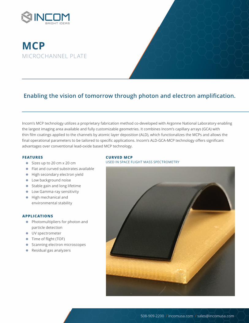
CURVED MCPUSED IN SPACE FLIGHT MASS SPECTROMETRY
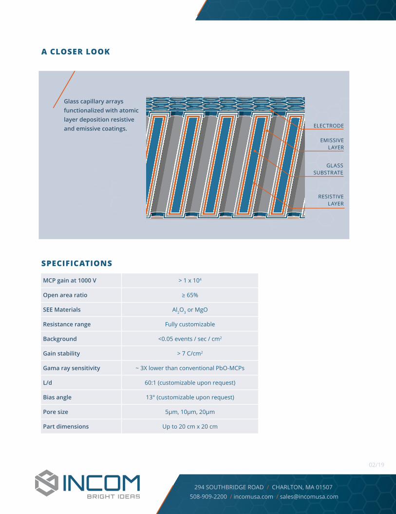
A CLOSER LOOK
Glass capillary arrays functionalized with atomic layer deposition resistive and emissive coatings.
294 SOUTHBRIDGE ROAD / CHARLTON, MA 01507508-909-2200 / incomusa.com / [email protected]
SPECIFICATIONS
MCP gain at 1000 V > 1 x 10⁴
Open area ratio ≥ 65%
SEE Materials Al2O3 or MgO
Resistance range Fully customizable
Background <0.05 events / sec / cm2
Gain stability > 7 C/cm2
Gama ray sensitivity ~ 3X lower than conventional PbO-MCPs
L/d 60:1 (customizable upon request)
Bias angle 13° (customizable upon request)
Pore size 5μm, 10μm, 20μm
Part dimensions Up to 20 cm x 20 cm
ELECTRODE
EMISSIVE LAYER
GLASS SUBSTRATE
RESISTIVE LAYER
02/19