metrology for emerging materials, devices, and structures
TRANSCRIPT
cnse.albany.edu
Metrology for Emerging Materials, Devices, and Structures: Graphene as an Example
Alain C. DieboldCenter for Nanoscale Metrology
(NC)3

cnse.albany.edu
Outline
• Characterization and Metrology• Physical Properties of Graphene• Optical Microscopy• LEEM• LEED• HR-TEM• Electrical Characterization• Overriding Themes

cnse.albany.edu
Characterization and Metrology: Themes
• Nano-Scale and Quantum Phenomena
• Familiar Methods show a “new light”
• New Methods always help
• Advancements still Required

cnse.albany.edu
Properties of Graphene
• High Mobility~ 100,000 cm2/V sec (few degrees Kevin) ~ 10,000 cm2/V sec (room temperature)
• Can carry high current density
• Robust Material
cnse.albany.edu
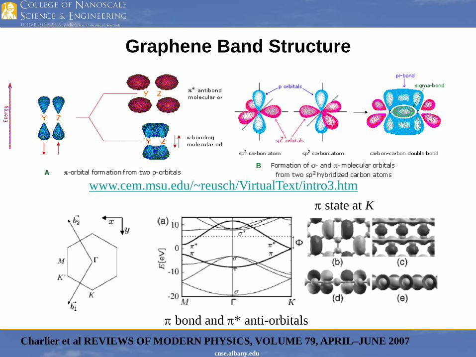
Graphene Band Structure
www.cem.msu.edu/~reusch/VirtualText/intro3.htm
Charlier et al REVIEWS OF MODERN PHYSICS, VOLUME 79, APRIL–JUNE 2007
π state at K
π bond and π* anti-orbitals

cnse.albany.edu
Graphene Electrical Properties• Semiconductors
– Parabolic Dispersion of Energy vs momentum
– Effective Mass defined by change of E vs k
• Graphene– Linear Dispersion of energy levels vs
momentum (wave vector k)
– light-like linear electronic band dispersion implies massless particles
– Particles called Dirac Fermions
See p 684 Charlier et al
m* = h2 /(d2 E/d2k)
E = h2k2/2m
E = h c

cnse.albany.edu
Graphene
Sources of Graphene
Exfoliation – Scotch tape & graphite
Reaction of SiC(0001)
Other
Bernal
Bernal Stacking vs Misorientation
Single Layer Properties for misoriented (AA’)No-Dirac Fermions for 2 to 4 layer Bernal
Inter-layer spacin 3.33 Å for B and 3.42 Å for turbostratic stacked bi-layer
Other mis-orientations possible
Latil, Meunier, and Henrard, PRB 76, 201402_R (2007)
38.21º

cnse.albany.edu
Optical MicroscopyThe magic 300 nm SiO2 substrate
Graphine is modeled as a 0.34 nm thick graphite layer
Graphite refractive index constant Between 400 nm to 750 nm
n = 2.6 – i 1.3
Contrast dependence is a result of wavelength dependence of SiO2 reflectivity
SiO2 reflectivity function of SiO2 thickness
Blake, et al., Appl. Phys. Lett. 91, (2007), 063124

cnse.albany.edu
Nano Scale Optical PropertiesOptical Properties of Graphene defined solely by
the Fine Structure Constant
• Dynamic Conductivity, G= e2/4h, of Dirac Fermions
• Fine Structure Constant α = e2/hc ≈1/137
• T ≡ (1 + 2πG/c)–2 = (1 + ½ πα)-2
• R ≡ ¼ π2α2T
Nair et al, Manchester group in Science 320, (2008), 1308

cnse.albany.edu
Remember Surface Analysis Methods - LEEM
Figures from J. Thorp /UVa, R. Hull (INDEX)/RPI, R. Tromp /IBM
Monolayer Sensitivity

cnse.albany.edu
LEEM analysis of Multilayer Graphene
3.5 eV 4 eV
4.5 eV 5 eV
Figure courtesy H. Hibino: Phys. Rev. B. 77, (2008), 075413.
Electron reflectivity from graphene on SiC(0001) shows quantized oscillations due to quantum well (QW) resonances.
When the LEEM electron energy matches that of one of the QW states, the electron transmits through the film reducing the reflectivity
2 ML
3 ML
4 ML5 ML
1 ML has one minimum in reflectance curve

cnse.albany.edu
Remember Surface Analysis Methods - LEED
Low Energy Electron Diffraction
Si (111) 7 x7 reconstruction
NIST Surface Science Database & www.cem.msu.edu/~cem924sg/

cnse.albany.edu
LEED Analysis of Graphene
Knox (Osgood Group at Columbia) AVS 2009
cnse.albany.edu
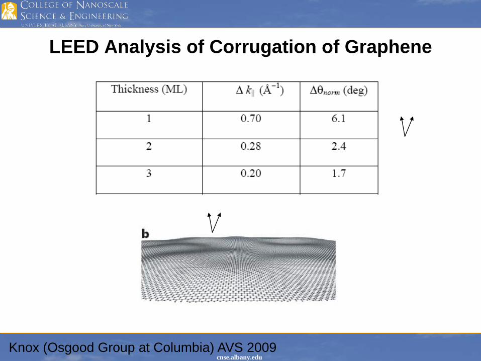
LEED Analysis of Corrugation of Graphene
Knox (Osgood Group at Columbia) AVS 2009

cnse.albany.edu
Remember Surface Analysis Methods – (AR)XPS
Ohta, Bostwick, Seyller, Horn, & Rotenburg, Science 313, (2006), p 951 & Nature Physics 3 (2007), p 36.
• ARXPS maps VB structure
• Bands not described by simple tight binding model
• Quasiparticles observed – e.g., electrons surrounded by phonons
• Potassium Doping opens band gap
• May explain impact of substrate on graphene electrical properties

cnse.albany.edu
Raman of Graphene
See for example: Ni Raman spectroscopy and imaging of graphene

cnse.albany.edu
Raman of GrapheneThe molecular picture
D band attributed to the breathing modes of sp2-bonded atoms in rings
Benzene Breathing Mode

cnse.albany.edu
Graphene’s Phonon Dispersion
J. Maultzsch et al, Phys. Rev. Lett. 92, (2004) 075501
G band
2D band is at ~2700 cm-1 due to a 2 phonon double resonant process involving π band
Wave vector K =0 Zone Center

cnse.albany.edu
Raman 2D Band Sensitive to # graphene layers
2657
2691 2708.5
2722
2600 2700 2800
2684.96
2655.05
2686.875 2707
2722
n=1
n=2
n=3
Inte
nsity
(a.u
)
2D Band
Raman Shift (cm-1)
Figure Courtesy Robert Geer CNSE (INDEX)
cnse.albany.edu
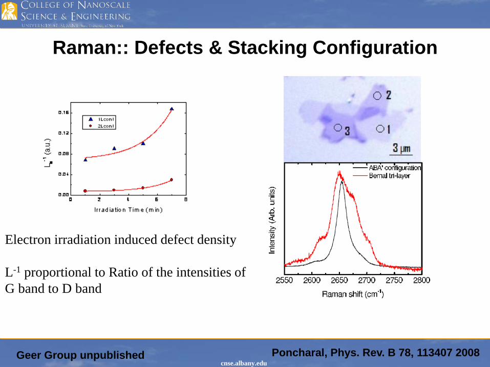
Raman:: Defects & Stacking Configuration
Electron irradiation induced defect density
L-1 proportional to Ratio of the intensities of G band to D band
Geer Group unpublished Poncharal, Phys. Rev. B 78, 113407 2008

cnse.albany.edu
NanoCharacterization of NanotubesAberration Corrected HR-TEM Imaging
Sloan, et al, MRS Bulletin, April 2004
Focal Series Corrected
Not Corrected
I KK II KK II K
Atomic Columns
Both K and I atomic columns are imaged
Heavy atom (Iodine) atomic columns are imaged

cnse.albany.edu
Multi-Slice Simulations of Graphene Stacking
F. Nelson (INDEX) this conference
Carbon Nanofilm
Horiuchi, et al.
AAA ABA ABC
-150A Defocus, 4% Noise
*C5=5mm, 0.15 Convergence angle
AAA ABA ABC
-150A Defocus, 2% Noise
Trilayer Graphene at 80kV, 0 CS

cnse.albany.edu
Aberration Corrected TEMFirst Images of Single Layer Graphene showing
atomic structure
Simulated HR TEM Image at 300 keV with Cs = 0
TEAM TEM 80 keV Cs = -17 um
Figure Courtesy C. Kisielowski - Nano Lett.8, (2008), 3582–3586

cnse.albany.edu
Observation of Corrugation: TEM Nano-Diffraction
Length ~ 25 nm
Height ~1 nm
J.C. Meyer, Nature 446, (2007), 60.

cnse.albany.edu
2009 – Aberration Corrected TEM of Stacking2 – Layers with 30º Misorientation
Warner, et. al. (Briggs), Nano Letters (2009), 102
Bi-LayerGraphene
ReconstructedImage
Back Layer
FFT
Front Layer

cnse.albany.edu
Hall MeasurementsCarrier Sheet DensityNS= IB / (q|VH|)
Determine the sheet resistance RS using a van der Paw test structure
Mobilityµ = |VH|/(RSIB) = 1/(qNSRS).
Quantum Hall Effect
σ = v e2/h - conductivitywhere v is either and integer or rational
fraction

cnse.albany.edu
Graphene Mobility Data
Zhang, et al, Nature 438, 201 (2005)
Suspended graphene sheetRed is after annealing
Bolotin et al Sol. State Com. 146, (2008), 351-355

cnse.albany.edu
Quantum Hall Effect
• In a Magnetic Field the Electrons have circular cyclotron orbits ωC = (eB/mc)
• When orbits are treated QM they have discrete energy levels – Landau Levels En = (h/2π)ωC(n+1/2)
• At certain values of field, energy levels a filled up to N and there is no electron scattering
• Conductivity σ will have discrete steps gse2/h where gs is the degeneracy factor (spin & sublevels) σ ~ N e2/h
Jx (Hall current) = σxy Ey Jy (current) = σyy Ey

cnse.albany.edu
Quantum Hall Effect in Graphene σ ~ (n+1/2)e2/h
Zhang, et al, Nature 438, 201 (2005)
Stormer and Kim - QHE proves Dirac nature of carriers

cnse.albany.edu
Berry Phase – angle of vector quantities in closed loop path
http://www.mi.infm.it/manini/berryphase.html

cnse.albany.edu
Nanoscale Quantum PhenomenaThe Berry Phase (angle) in Graphene confirms Dirac particle
• At low magnetic fields, Shubnikov de Hass oscillations in the resistance Rxx perpendicular to current flow.
• ∆Rxx = A cos[2π(BF/B + ½ + β)]
• β (Berry Phase) = ½ for Dirac particles
• BF is frequency SdH oscillations
• B is magnetic field strengthBerry Phase, β, refers to correction to semiclassical dynamics
– not needed when a full QM theory is used.Zhang, et al, Nature 438, 201 (2005)

cnse.albany.edu
Single Electron MicroscopyElectron Hole Puddles –
Are they due to Graphene Corrugation from SiO2?
X
Y
Single Electron Transistor
J. Martin, et al, Nature Physics, 4, (2008), 144-148.
“The SET tip is capable of measuring the local electrostatic potential with microvolt sensitivity and a high spatial resolution close to its size.”
The intrinsic disorder length scale in graphene is ~ 30 nm.
SiO2
0.3K

cnse.albany.edu
Observation of Graphene Corrugation by STM
Corrugation has a height variation of 5 A over an area of 30 30 nm2.
Lateral extent of these corrugations ~ few nanometers
Corrugation mimics the SiO2 surface
Deshpande, Bao, Miao, Lau, and LeRoy, Spatially resolved spectroscopy of monolayer graphene on SiO2

cnse.albany.edu
STM Observation of Stacking Misorietation
Latil, Meunier, and Henrard, PRB 76, 201402_R (2007) 3 layer graphene on SiC

cnse.albany.edu
Graphene RibbonsCan We Measure properties of Ribbons?
Width of Graphene NanoRibbon
Ban
d G
ap
Han, et al (Kim’s Group), PRL 98, 206805 (2007)

cnse.albany.edu
What we can Measure
• Where graphene is (for some samples)
• Number of graphene layers & orientation
• Corrugation
• Electrical – mobility, carrier density, conductance

cnse.albany.edu
Conclusions
• Graphene displays novel properties due to nanoscale dimensions and unique electronic structure
• Metrology must continue to advance to meet needs of new materials such as graphene
• Despite these advances- metrology and device fabrication are amazingly difficult

cnse.albany.edu
Acknowledgements• Florence Nelson and Tianhao Zhang
• Christian Kisielowski
• Theme VI team – Ray Ashouri, Karl Berggren, Robert Geer, Julia
Greer, Tony Heinz, Robert Hull, Philip Kim, Charlie Marcus
• NRI – NERC – INDEX Funding