mems simulation and mask design - university of minnesota 11 mems simulatio… · mems simulation...
TRANSCRIPT

MEMS Simulation and Mask Design
Prof. Tianhong Cui, Mechanical Engineering
ME 8254

MEMS Design

Design, A TradeoffIterative Process
Find a solution that satisfies a set ofrequirements
Some requirements may have conflictedrequirements
Trade-offs have to be made Performance may not the only goal. It is
often traded off for manufacturability

Design, A TradeoffIterative Process
Adapted from
Wu, UC Berkeley
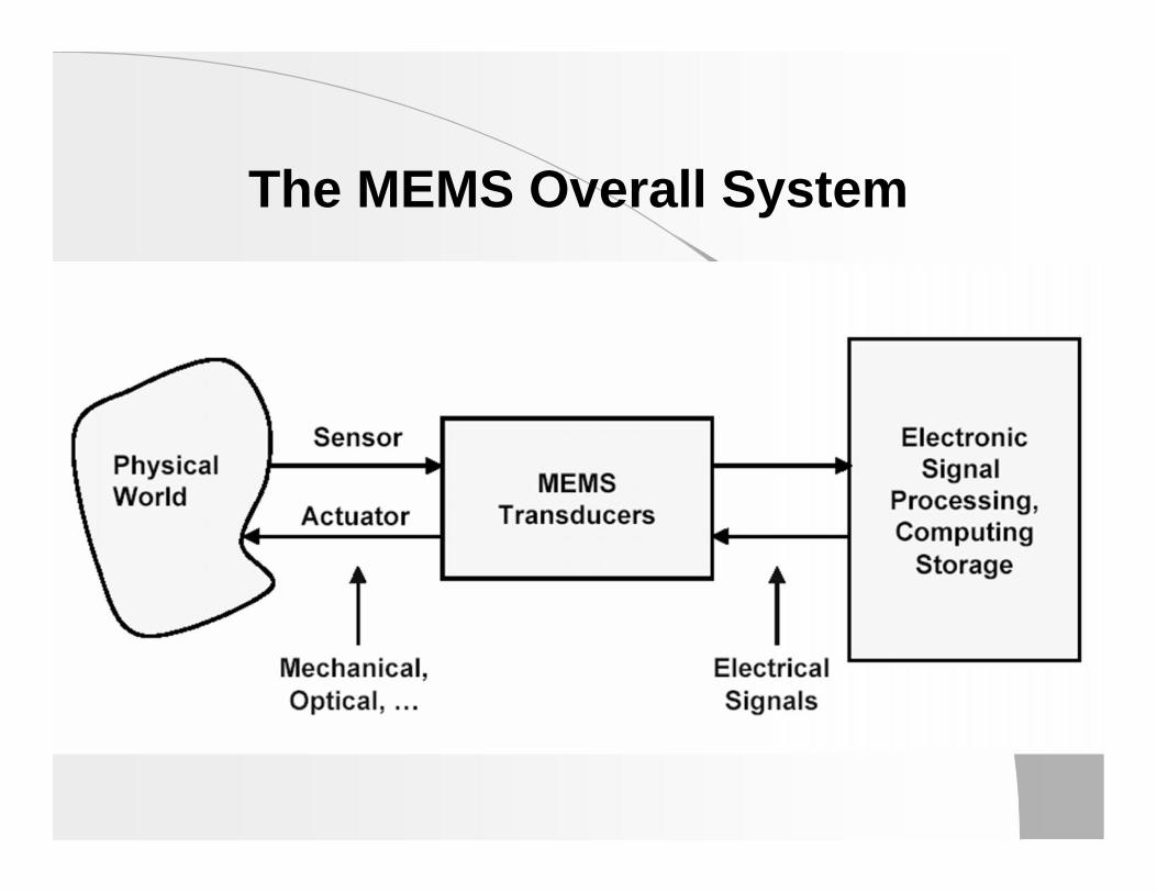
The MEMS Overall System

MEMS Design Framework

Design Issues

MEMS Design and Modeling

MEMS Design Process & Flow

Other MEMS Design Issue

CAD for MEMS Design

Definition of Computer Aided Designin Microsystems Technology
In MEMS technology, CAD is defined as atightly organized set of cooperating computerprograms that enable the simulation ofmanufacturing processes, device operation,and packaged Microsystems behavior in acontinuous sequence, by a microsystemengineer.

Commercial Software
Coventor Suite/MEMCAD by Coventor Inc.– http://www.coventor.com
Intellisuite by Intellisense Inc.– http://www.intellisense.com
MEMScap from MEMScap Inc.– http://www.memscap.com
SOLIDIS from ISE Inc.– http://www.ise.com

Task Sequence Accomplishedby a CAD Tool
Layout and process
Topography simulation
Boundaries, IC process results and Materialproperties
Mesh generation
Device simulation
System-Level Simulation
MEMS Control CAD

Layout and Process Resources
First Resource: The process description of theinterface and the driving circuitry:– Can be accomplished using a layout file editor (eg.
CADENCE, http://www.cadence.com or L-Edit,http://www.tanner.com)
Second Resource: The Process flow descriptionfile:– Relates a processing step to each lithography mask in
the layout file
– Can be optimized

Topography Simulation Goal: Obtain a realistic topography of the
considered device by:– Realistically representing complex 2D and 3D
structures to simulate the IC manufacturingprocess
– Can be accomplished using (among others): IntelliCAD from Intellisense Inc.
ACES from the University of Illinois at Urbana
MenBuilder from Coventor Inc

Boundaries, IC Process Resultsand Material Properties
Description of the material interfaceboundary
Dopant distribution within each layer of thedevice
Distribution of residual stresses
Optimization of material properties

Mesh Operations
Generate a computational mesh fordevice physics simulation by boundaryelement methods, finite elementmethods, or a coupling of both
Meshless methods being developed

Device Simulation
Compute the coupled response of aMEMS device using numericalmethods (FEA/BEA)
Also provide many coupling effect thatMEMS rely on (eg. electromechanical,thermomechanical, optoelectrical, andoptomechanical coupling behaviors)
Extract behavioral models for system-level simulation.

System-Level Simulation
Conversion of a numerical matrix to anequivalent subcircuit
Translate specific changes in deviceconfiguration, dimensions, andmaterial properties into the circuit-equivalent behavioral model

MEMS Control CAD
Development of automated algorithmicmethods for designing and controlling largecoupled groups of MEMS units
Development of micromanipulation workcellto assemble automatically MEMS parts

Packaging Simulation
Automated package-device interactionsimulation by:
– Separating FEA of both the package and thedevice
– Coupling the results through parametricbehavioral package models (Coventor Suite)

Modeling EngineeringSystems

Modeling Engineering Systems
We separate out modeling into three areas:
1) Mathematical Modeling
2) Numerical Modeling
3) Computational Modeling.
These are not really three distinct entities, but ratherare related by the fact Mathematical Modeling is asubset of Numerical Modeling, and bothMathematical and Numerical Modeling are subsetsof Computational Modeling.

It is important to note that each type of modeling hasits advantages and drawbacks. Of course, theoptimal goal of modeling is to attain the "best"simulation of a realistic physical system with the"least" amount of headache.
The "best" simulation is that it gives the mostaccurate description of physical behavior for agiven system. It is critical to remember that whenwe model a system, we will never completelydescribe all the behavior of that system.

We must make assumptions as to what aspects of thesystem behavior are most important to "catch" inour model.
We often have to reach a compromise between theneed to represent a system as accurately aspossible with our ability to both create and solveour representation or model of the system.
Finally, always, always remember that no model is100% accurate.

Mathematical Modeling
Mathematical modeling is the oldest basis for analyzingphysical systems. Mathematical modeling involvesdescribing the physics of a system by partialdifferential equations (PDE).
The PDE are developed by balancing fluxes on aninfinitesimal element. By assuming this flux balance,we derive the standard elliptic PDE describing thephysics of static systems and the hyperbolic PDEdescribing the physics of dynamic systems.

The assumptions we make are that the material is subjectto a certain flux of energy, such as thermal,mechanical, etc.
Using only mathematical modeling requires that we solvethe PDE analytically. Although the advantage of doingthis is that we have a compact description of thephysical field within the system, the drawback is that itis almost never possible to generate an analyticalsolution except for the simplest systems.
Physical systems have more complicated materialdistributions, more complicated domains, and morecomplicated boundary conditions which create verycomplicated analytical solutions.

Numerical Modeling Numerical modeling is a superset of mathematical
modeling. Numerical modeling contains the originalmathematical modeling descriptions, but createsapproximations to mathematical model solutions.
Well-known examples of numerical modelinginclude Fourier solutions to differential equations,Ritz methods and Runge Kutta time integrationschemes. Numerical modeling essentially converts ananalytical solution into an approximate algebraicsolution to determine the unknown coefficients.

Although numerical modeling is now integratedclosely with the computer, many numericalapproximation methods were developed starting inthe late 18th century.
In addition, numerical solutions to mathematicalPDE were carried out well before the development ofthe computer, although the computer has obviouslyenhanced the use of numerical methods.
Numerical methods really represent an advance inthe processing portion of modeling. For instance, wecan apply numerical solution methods for problemswhose material, domain and boundary conditions wecan describe by paper and pencil.

Computational Modeling Computational modeling represents the largest set of
modeling techniques in our description.
Computational modeling is based on the PDEdescription of physics from mathematical modeling, andalso utilizes the solution approximations made innumerical modeling.
What sets computational modeling apart frommathematical and especially numerical modeling is thatnow we must use a computer not only to solve ournumerical approximation, we must also use otheraspects of computing like computer graphics,visualization and imaging to set up our mathematicaldescription.
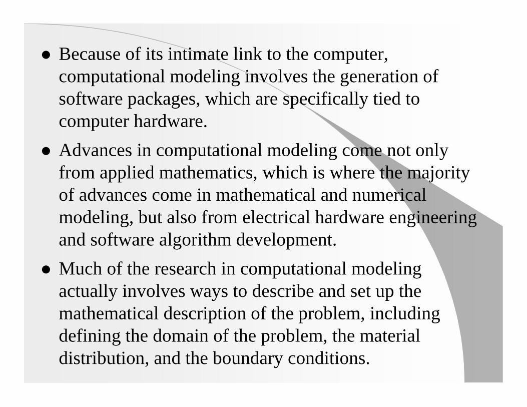
Because of its intimate link to the computer,computational modeling involves the generation ofsoftware packages, which are specifically tied tocomputer hardware.
Advances in computational modeling come not onlyfrom applied mathematics, which is where the majorityof advances come in mathematical and numericalmodeling, but also from electrical hardware engineeringand software algorithm development.
Much of the research in computational modelingactually involves ways to describe and set up themathematical description of the problem, includingdefining the domain of the problem, the materialdistribution, and the boundary conditions.

Computational modeling is ubiquitous within engineering today.Finite element and finite difference software systems are usedextensively to design and analyze products.
However, although these software systems, extensively based onthe geometry paradigm we discuss next, have greatly enhancedthe modeling process, they by no means are a utopia.
Modeling extremely complex systems still takes a significantamount of time, sometimes too long to be of use in making theproduct.
For biological tissues, the complexity of anatomy and tissuestructure often make the traditional geometry paradigm oflimited value. For this reason, the idea of image based CAE,proposed by a number of researchers, has taken hold inbiomedical engineering, but is also taking hold in traditionalengineering.

Finite ElementAnalysis and Design
Microsystems/MEMS Engineering

MEMS Modeling Levels Process level: reflecting fabrication steps and their
effects on device geometry and materials properties
Physical level: reflecting the response of the 3Ddevice continuum (3D FEA)
Device level: reflecting macro-model or low-orderextracted models from physical models (simplespring elements)
System level: reflecting system behavior integratingmechanics and electronics through behavioral modelthat can be simulated in Simulink and alike.

Mask Design and Fabrication

Lithography Processing
Negative Resist
Positive Resist
Both microelectronics andMEMS fabrication start withlithography

Mask
The stencil used to repeatedlygenerate a design pattern onresist-coated wafers is called amask
The lithographic patterns printed ona wafer need to be as good aspatterns on the mask

Mask Type
Binary Mask
Proximity correction mask
Phase shift mask

Binary Mask
The pattern area is either clearor opaque
The mask pattern design is thesame as the desired pattern of thedevice
May cause serrated edges andnon-uniformity across the mask

Proximity Correction Mask
Modify themask pattern Final mask
pattern maycontain serifsat featurecorners

Phase Shift Mask
Add one 180° phase shift layer on a mask The feature size can be about 100 nm First was introduced in 1982. New software
developed.

Mask Principal Parameters
Pattern position accuracy
Feature size control
Defect and pattern fidelity

Pattern Position Accuracy
It refers to the pattern alignmentbetween two or more criticalmask levels of a given set.
It is important to know and measurethe machine error that affects thepattern position accuracy

Feature Size Control
Critical dimension control (CD) isone/more features defined bya designer
Three important parameters:1. The average value of a given critical
dimension for the specified value.2. The uniformity of the critical dimension.3. The linearity of feature sizes down to some
lower limits.

Defects and Pattern Fidelity
Defects may be defined as extraor missing parts of a chromium film
Pattern fidelity covers many issuessuch as incorrect pattern shape. Itis also defined by the pixel size usedto write the pattern

Mask Design
Design sequence
Design consideration
An example - micromotor

Design Sequence
Device design Pattern design Process design Drawing your mask pattern

Design Consideration
Minimum feature size Pattern uniformly Positive/negative photoresist Alignment marks Bonding requires

An Example - Micromotor
Electrostaticforce
Rotor: 120 µmin diameter
Six masksprocess design

Mask for Micromotor

Exposure and Alignment Tool

Mask and Substrate Holder
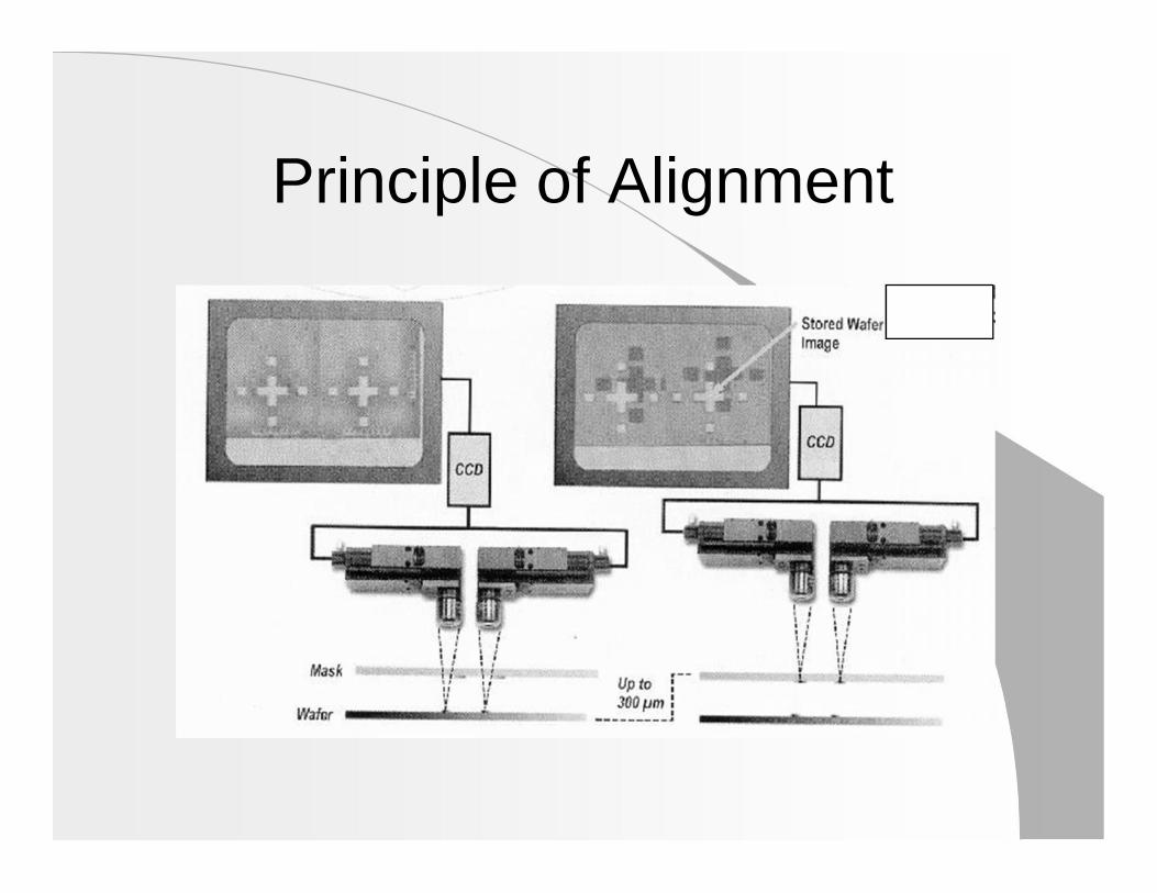
Principle of Alignment
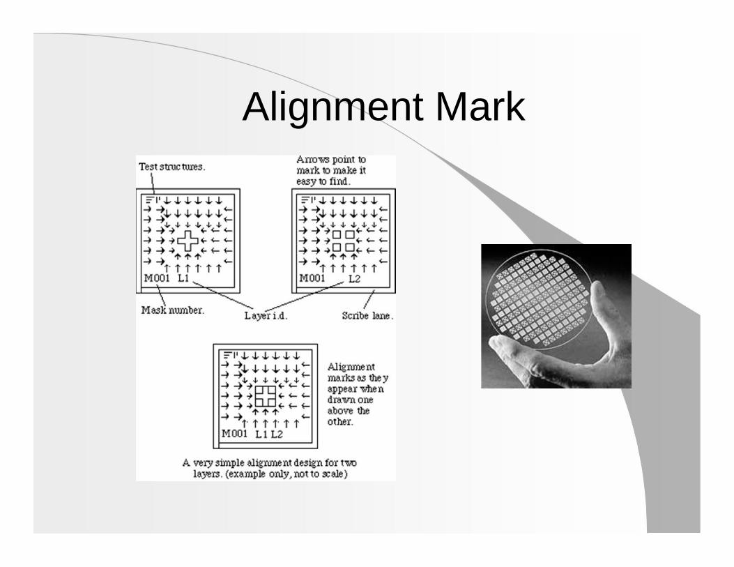
Alignment Mark

Mask Design Tools
AutoCAD L-edit Some simulation tools:
MAMSCAD; Intellsense Link CAD

L-Edit Main Setting
Technology file – store the preferencelayer name, layer number, screencolor, internal units, ……
Grid – basic mesh dimensionvariable, snap, ……
Text – type text on your layout Format – GDSII, CIF, TDB, ……

Mask Making
Pathway pattern transfer Emulsion mask and Chrome mask Fabrication tools and steps

Fabrication Procedures
Substrate preparation Pattern writing Pattern processing Metrology Inspection for pattern integrity Cleaning Repair Pellicle attachment Final defect inspection

Mask Fabrication Tool
High resolution printer
Optical pattern generator
E-beam writer