measuring jitter in digital systems -...
TRANSCRIPT

Measuring Jitter in Digital Systems Application Note
Measuring jitter in digital systems
The topic of jitter is becoming increasingly critical to the proper design of digital subsystems. In the past, digital designers were largely concerned with functional issues. Now, in addition to debugging the functionality of a design, digital designers are also called upon to investigate paramet-ric issues. These parametric issues have a significant impact on the design, operation, and proof of operation of a digital product.
At bit transfer rates exceeding tens of gigabits per second, the analog nature of signals can become frustratingly appar-ent. Designers can no longer remain in the ideal binary realm of 1s and 0s, verifying that their logic performs its functions. They must also move into the parametric realm, dealing with ambiguity and measuring how well their designs work.
As new data transfer standards move into their third and fourth generations with ever faster bit transfer rates are pro-posed and implemented, designers must concern themselves with the true analog nature of electronic signals: there may be digital circuits that transfer binary data, but there really is no such thing as a digital waveform.
This application note is for engineers who design data trans-fer systems and components operating at over a gigabit per second, and so must be concerned with the effects of jitter on their system’s bit error ratio (BER).
Table of Contents
Measuring jitter in digital systems ......................................... 1Why measure jitter? .................................................................. 2Eye diagrams portray jitter intuitively .................................... 2Jitter reduction requires a multifaceted view ...................... 3Jitter characteristics depend on its sources ........................ 4Bounded/deterministic vs unbounded/random jitter ......... 4Calculating total jitter ................................................................ 5A case study: jitter evaluation on an eye diagram............... 6Jitter measurement viewpoints .............................................. 7Eye diagrams revisited .............................................................. 8Histograms .................................................................................. 8The bathtub plot ......................................................................... 9Frequency-domain jitter views .............................................. 10Separating random and deterministic jitter ........................ 11Jitter tolerance and jitter transfer ........................................ 12Tools for measuring & viewing jitter .................................... 13Pulse/pattern generator ......................................................... 13Low-level phase-noise/spectrum analyzer ......................... 13Real-time sampling oscilloscopes ........................................ 14Digital communications analyzers (DCAs) .......................... 14Bit error ratio testers (BERTs) ............................................... 15Logic analyzers with EyeScan ............................................... 15References ................................................................................ 15
2
Why measure jitter?
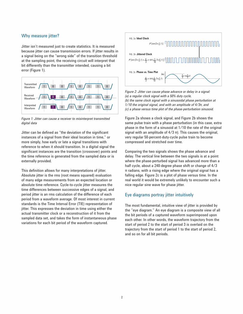
Jitter isn’t measured just to create statistics. It is measured because jitter can cause transmission errors. If jitter results in a signal being on the “wrong side” of the transition threshold at the sampling point, the receiving circuit will interpret that bit differently than the transmitter intended, causing a bit error (Figure 1).
Figure 1: Jitter can cause a receiver to misinterpret transmitted digital data
Jitter can be defined as “the deviation of the significant instances of a signal from their ideal location in time,” or more simply, how early or late a signal transitions with reference to when it should transition. In a digital signal the significant instances are the transition (crossover) points and the time reference is generated from the sampled data or is externally provided.
This definition allows for many interpretations of jitter. Absolute jitter is the rms (root means squared) evaluation of many edge measurements from an expected location or absolute time reference. Cycle-to-cycle jitter measures the time differences between successive edges of a signal, and period jitter is an rms calculation of the difference of each period from a waveform average. Of most interest in current standards is the Time Interval Error (TIE) representation of jitter. This expresses the deviation in time using either the actual transmitter clock or a reconstruction of it from the sampled data set, and takes the form of instantaneous phase variations for each bit period of the waveform captured.
1 0 0 1 0 1 1 0
1 1 0 1 0 1 1 0
1 0 0 1 0 1 1 0TransmittedWaveform
ReceivedWaveform
InterpretedWaveform
Dϕ
P [sin
P [sin ]
FIG. 2b Jittered Clock
FIG. 2a Ideal Clock
FIG. 2c Phase vs. Time Plot
Figure 2: Jitter can cause phase advance or delay in a signal: (a) a regular clock signal with a 50% duty cycle, (b) the same clock signal with a sinusoidal phase perturbation at 1/10 the original signal, and with an amplitude of 4/3π, and (c) a phase versus time plot of the phase-perturbation sinusoid.
Figure 2a shows a clock signal, and Figure 2b shows the same pulse train with a phase perturbation (in this case, extra phase in the form of a sinusoid at 1/10 the rate of the original signal with an amplitude of 4/3 π). This causes the original, very regular 50-percent-duty-cycle pulse train to become compressed and stretched over time.
Comparing the two signals shows the phase advance and delay. The vertical line between the two signals is at a point where the phase-perturbed signal has advanced more than a half cycle, about a 240-degree phase shift or change of 4/3 π radians, with a rising edge where the original signal has a falling edge. Figure 2c is a plot of phase versus time. In the real world it would be extremely unlikely to encounter such a nice regular sine wave for phase jitter.
Eye diagrams portray jitter intuitively
The most fundamental, intuitive view of jitter is provided by the “eye diagram.” An eye diagram is a composite view of all the bit periods of a captured waveform superimposed upon each other. In other words, the waveform trajectory from the start of period 2 to the start of period 3 is overlaid on the trajectory from the start of period 1 to the start of period 2, and so on for all bit periods.
3
LeftCrossing
Point
RightCrossingPoint
X
SamplingPoint
One Unit IntervalOne Bit Period
Figure 3: An idealized eye diagram
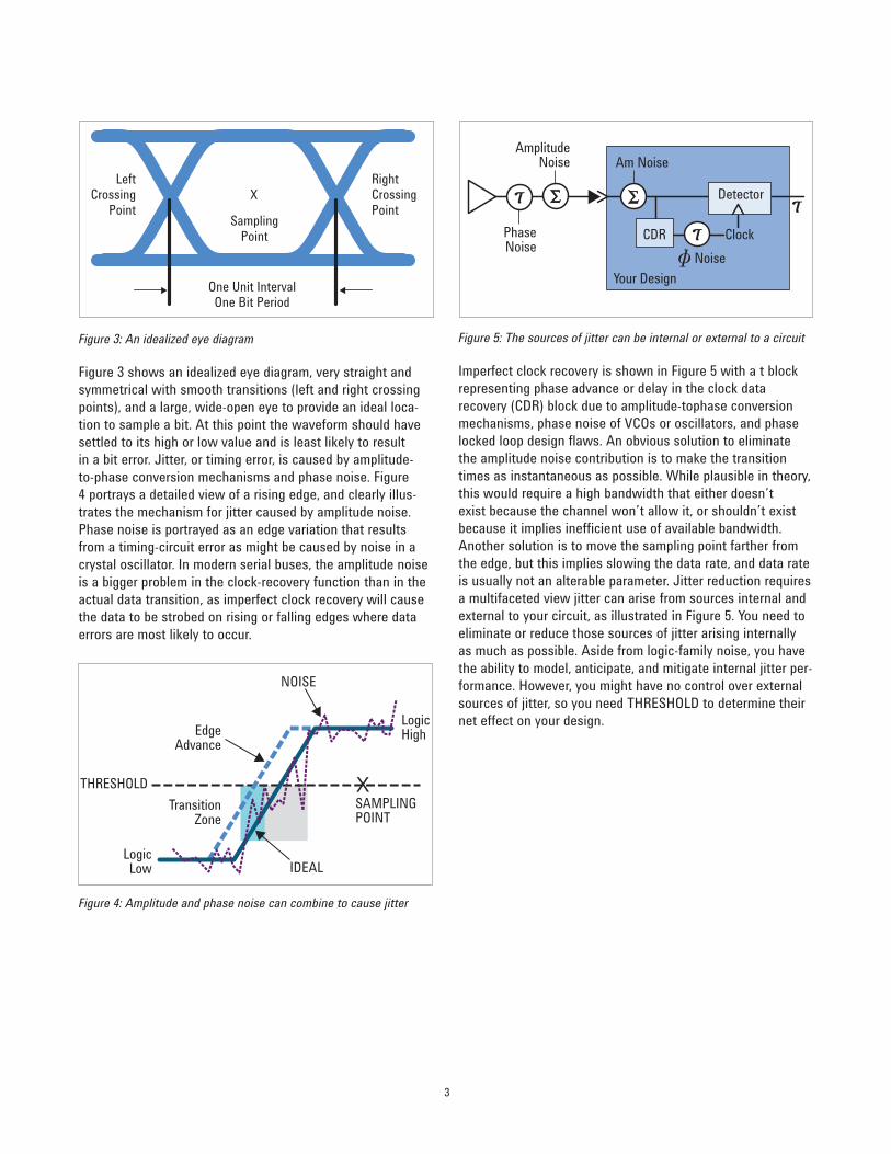
Figure 3 shows an idealized eye diagram, very straight and symmetrical with smooth transitions (left and right crossing points), and a large, wide-open eye to provide an ideal loca-tion to sample a bit. At this point the waveform should have settled to its high or low value and is least likely to result in a bit error. Jitter, or timing error, is caused by amplitude-to-phase conversion mechanisms and phase noise. Figure 4 portrays a detailed view of a rising edge, and clearly illus-trates the mechanism for jitter caused by amplitude noise. Phase noise is portrayed as an edge variation that results from a timing-circuit error as might be caused by noise in a crystal oscillator. In modern serial buses, the amplitude noise is a bigger problem in the clock-recovery function than in the actual data transition, as imperfect clock recovery will cause the data to be strobed on rising or falling edges where data errors are most likely to occur.
X
NOISE
IDEAL
SAMPLINGPOINT
LogicHigh
LogicLow
TransitionZone
EdgeAdvance
THRESHOLD
PhaseNoise
AmplitudeNoise Am Noise
Detector
Clock
Your Design
CDR
Figure 5: The sources of jitter can be internal or external to a circuit
Imperfect clock recovery is shown in Figure 5 with a t block representing phase advance or delay in the clock data recovery (CDR) block due to amplitude-tophase conversion mechanisms, phase noise of VCOs or oscillators, and phase locked loop design flaws. An obvious solution to eliminate the amplitude noise contribution is to make the transition times as instantaneous as possible. While plausible in theory, this would require a high bandwidth that either doesn’t exist because the channel won’t allow it, or shouldn’t exist because it implies inefficient use of available bandwidth. Another solution is to move the sampling point farther from the edge, but this implies slowing the data rate, and data rate is usually not an alterable parameter. Jitter reduction requires a multifaceted view jitter can arise from sources internal and external to your circuit, as illustrated in Figure 5. You need to eliminate or reduce those sources of jitter arising internally as much as possible. Aside from logic-family noise, you have the ability to model, anticipate, and mitigate internal jitter per-formance. However, you might have no control over external sources of jitter, so you need THRESHOLD to determine their net effect on your design.
Figure 4: Amplitude and phase noise can combine to cause jitter
4
By representing jitter in terms of phase perturbation only, it is possible to consider different domains for analysis. In mathematical terms, the phase error (advance or delay) is generalized with the function ϕj (t), so the equation for a pulsed signal affected by jitter becomes:
S(t) = P [2πƒdt + ϕj (t)],
where P is used to denote a sequence of periodic pulses.
This leads to mathematically equivalent expressions for jitter. Since the argument of the function is in radians, dividing Δϕ (peak or rms phase) by 2π expresses jitter in terms of the unit interval (UI), or bit period (for the pulses):
J(UI) = ( )
Unit interval expression is useful because it allows immediate comparison with the bit period and a consistent comparison of jitter between one data rate or standard and another.
Dividing the jitter in unit intervals by the frequency of the pulse (or multiplying by the bit period) yields the jitter in time units:
J(t) = ( )
Viewing jitter as phase variation leads to three ways of expressing or representing jitter, and therefore to three domains for analysis, to build that comprehensive view of the jitter affecting your circuit. The three domains or approaches for jitter analysis each provides its own insight into the nature of the jitter affecting the measured device. Jitter can be analyzed in the time domain (jitter amplitude versus time), the modulation domain (radians versus time, phase versus time, and time versus time), and the frequency domain (amplitude of jitter components versus their frequency, or analysis of phase modulation sidebands).
Δϕ2π
Δϕ2πƒd
Jitter characteristics depend on its sources
Jitter on a signal will have different characteristicsdepending on its causes, so categorizing the sources ofjitter becomes important for measuring and analyzingjitter. The first category is random noise mechanisms,processes that randomly introduce noise to a system. These sources include:
• thermal noise (KTB noise, which is associated with electron flow in conductors and increases with band-width, temperature, and noise resistance)
• shot noise (electron and hole noise in a semiconductor, which rises depending on bias current and measurement bandwidth)
• flicker (pink) noise (noise that is spectrally related to 1/ƒ)
These exist in all semiconductors and components, and play the most significant roles in phase locked loop designs, oscil-lator topologies and designs, and crystal performance.
The second category is system mechanisms, effects on a signal that result from characteristics of its digital system. Examples of system-related noise sources include:
• crosstalk from radiated or conducted signals
• dispersion effects
• impedance mismatch
The third category is data-dependent mechanisms, those in which the patterns or other characteristics of the data being transferred affect the net jitter seen in the receiver. Data-dependent jitter sources include:
• intersymbol interference
• duty-cycle distortion
• pseudo random bit sequence periodicity
Bounded/deterministic vs unbounded/random jitter
Often the sources of jitter are categorized into two types, bounded and unbounded. Bounded jitter sources reach maximum and minimum phase deviation values within an identifiable time interval. This type of jitter is also called deterministic, and results from systematic and data-depen-dent jitter-producing mechanisms (the second and third groups identified above).
5
Unbounded jitter sources do not achieve a maximum or minimum phase deviation within any time interval, and jitter amplitude from these sources theoretically approaches infin-ity. This type of jitter is referred to as random and results from random noise sources identified in the first group above. So the total jitter on a signal, specified by the phase error func-tion ϕj (t), is the sum of the deterministic and random jitter components affecting the signal:
ϕj (t) = ϕj (t)D + ϕj (t)R.
ϕj (t)D, the deterministic jitter component, related as a peak-to-peak value, Jpp
D, is determined by adding the maximum phase (or time) advance and phase (or time) delay produced by the deterministic (bounded) jitter sources.
ϕj (t)R, the random jitter component, related as a standard deviation value, Jrms
R, is a composite of all random noise sources affecting the signal. Random jitter is assumed to fol-low a Gaussian distribution, and is defined by the mean and sigma of that Gaussian distribution. To determine the jitter produced by the random noise sources, the Gaussian function representing this random jitter must be determined and its sigma evaluated.
Calculating total jitter
To calculate the total jitter on a signal, the Gaussian random jitter and the peak-to-peak deterministic jitter must be combined in such a manner as to support the expected BER performance of the underlying digital link. In order to arrive at this relation (to BER), the random and deterministic compo-nents must be understood separately.
As previously mentioned, the deterministic component of jitter is determined by calculating the greatest difference in time for transitions across the digital circuit threshold due to deterministic sources. It is denoted as Jpp
D.
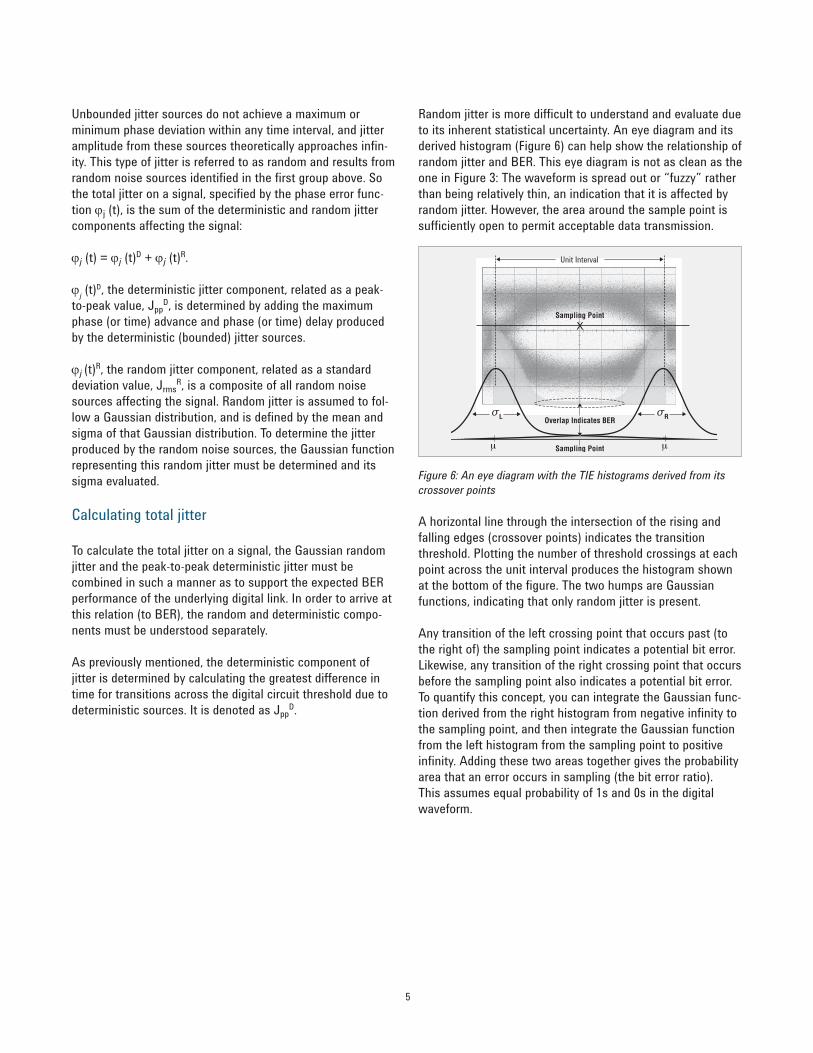
Random jitter is more difficult to understand and evaluate due to its inherent statistical uncertainty. An eye diagram and its derived histogram (Figure 6) can help show the relationship of random jitter and BER. This eye diagram is not as clean as the one in Figure 3: The waveform is spread out or “fuzzy” rather than being relatively thin, an indication that it is affected by random jitter. However, the area around the sample point is sufficiently open to permit acceptable data transmission.
Unit Interval
Figure 6: An eye diagram with the TIE histograms derived from its crossover points
A horizontal line through the intersection of the rising and falling edges (crossover points) indicates the transition threshold. Plotting the number of threshold crossings at each point across the unit interval produces the histogram shown at the bottom of the figure. The two humps are Gaussian functions, indicating that only random jitter is present.
Any transition of the left crossing point that occurs past (to the right of) the sampling point indicates a potential bit error. Likewise, any transition of the right crossing point that occurs before the sampling point also indicates a potential bit error. To quantify this concept, you can integrate the Gaussian func-tion derived from the right histogram from negative infinity to the sampling point, and then integrate the Gaussian function from the left histogram from the sampling point to positive infinity. Adding these two areas together gives the probability area that an error occurs in sampling (the bit error ratio). This assumes equal probability of 1s and 0s in the digital waveform.

6
The BER as a function of the sampling point location on the Gaussian curve, expressed as the number of sigma from the mean, has been calculated and tabulated. To achieve a BER of 10-12 (a common requirement of many modern standards), the crossover point of the signal must be at least 7σ from the sampling point (assumed here to be centrally located in the unit interval), or in other words, the signal must have a unit interval of at least 14σ. If the estimated sigma is too large, causing the sampling point to be less than 7σ from the mean on either crossover point, then you have a problem with random jitter alone, and you have to find a way to increase the unit interval (rarely an option) or reduce the random jitter (σ). If the space between the crossover point and the ideal sampling point is greater than 7σ, then you have some margin in achieving the required 10-12 BER. A list of the minimum number of sigma between crossover points for various BERs is shown in Figure 7.
BER Multiplier10-4 7.43810-6 9.50710-7 10.39910-9 11.99610-11 13.41210-12 14.06910-13 14.69810-15 15.883
Figure 7: Minimum number of sigma (multiplier factor) for various BERs
Keep in mind that this discussion so far applies to purely Gaussian functions with identical sigmas for the left and right distributions, which would be the case if they arise from purely random processes. In practice, however, these are not identical, so many standards stipulate that the sigmas be averaged to generate the effective process sigma, which pro-vides a good approximation given that the values are close.
Once the random jitter component (σ) has been statistically calculated, then it can be combined with the deterministic jitter components to obtain the total peak-to-peak jitter and determine whether it is within your system’s “jitter budget.” To combine these, use the worst-case deterministic value as the effective mean for the random Gaussian process (an acknowledgement that the deterministic processes and ran-dom processes are statistically independent). Then use the aforementioned process for determining random jitter again, but with a bias or time offset in the result. It thus follows that total jitter is calculated:
JTOTAL = 14σ+ JppD (for a BER of 10-12)
A case study: jitter evaluation on an eye diagram
Figure 8 is an eye diagram of a waveform that is even less ideal than the fuzzy eye diagram of Figure 6. However, the charac-teristics of its irregular shape reveal much about it, even with simple observation rather than complex measurements.
Figure 8: An eye diagram with an irregular shape
For one thing, the bottom appears to have a smaller amplitude variation than the top, so the signal seems to carry more 0s than 1s. There are four different trajectories in the bottom, so at least four 0s in a row are possible, whereas on top there appears to be no more than two trajectories, indicating the waveform contains at most only two 1s in a row. The wave-form has two different rising and falling edges, indicating the presence of deterministic jitter. The rising edges have a greater spread than the falling edges, and some of the cross-over points intersect below the threshold level, indicating duty-cycle distortion, with 0s having a longer cycle or on-time than 1s.
7
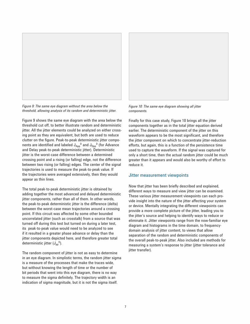
Figure 9: The same eye diagram without the area below the threshold, allowing analysis of its random and deterministic jitter.
Figure 9 shows the same eye diagram with the area below the threshold cut off, to better illustrate random and deterministic jitter. All the jitter elements could be analyzed on either cross-ing point as they are equivalent, but both are used to reduce clutter on the figure. Peak-to-peak deterministic jitter compo-nents are identified and labeled JApp
D and JDppD (for Advance
and Delay peak-to-peak deterministic jitter). Deterministic jitter is the worst-case difference between a determined crossing point and a rising (or falling) edge, not the difference between two rising (or falling) edges. The center of the signal trajectories is used to measure the peak-to-peak value. If the trajectories were averaged extensively, then they would appear as thin lines.
The total peak-to-peak deterministic jitter is obtained by adding together the most advanced and delayed deterministic jitter components, rather than all of them. In other words, the peak-to-peak deterministic jitter is the difference (delta) between the worst-case mean trajectories around a crossing point. If this circuit was affected by some other bounded uncorrelated jitter (such as crosstalk) from a source that was turned off during this test but turned on during a later test, its peak-to-peak value would need to be analyzed to see if it resulted in a greater phase advance or delay than the jitter components depicted here, and therefore greater total deterministic jitter (Jpp
D).
The random component of jitter is not as easy to determine in an eye diagram. In simplistic terms, the random jitter sigma is a measure of the processes that make the traces wide, but without knowing the length of time or the number of bit periods that went into this eye diagram, there is no way to measure the sigma definitely. The trajectory width is an indication of sigma magnitude, but it is not the sigma itself.
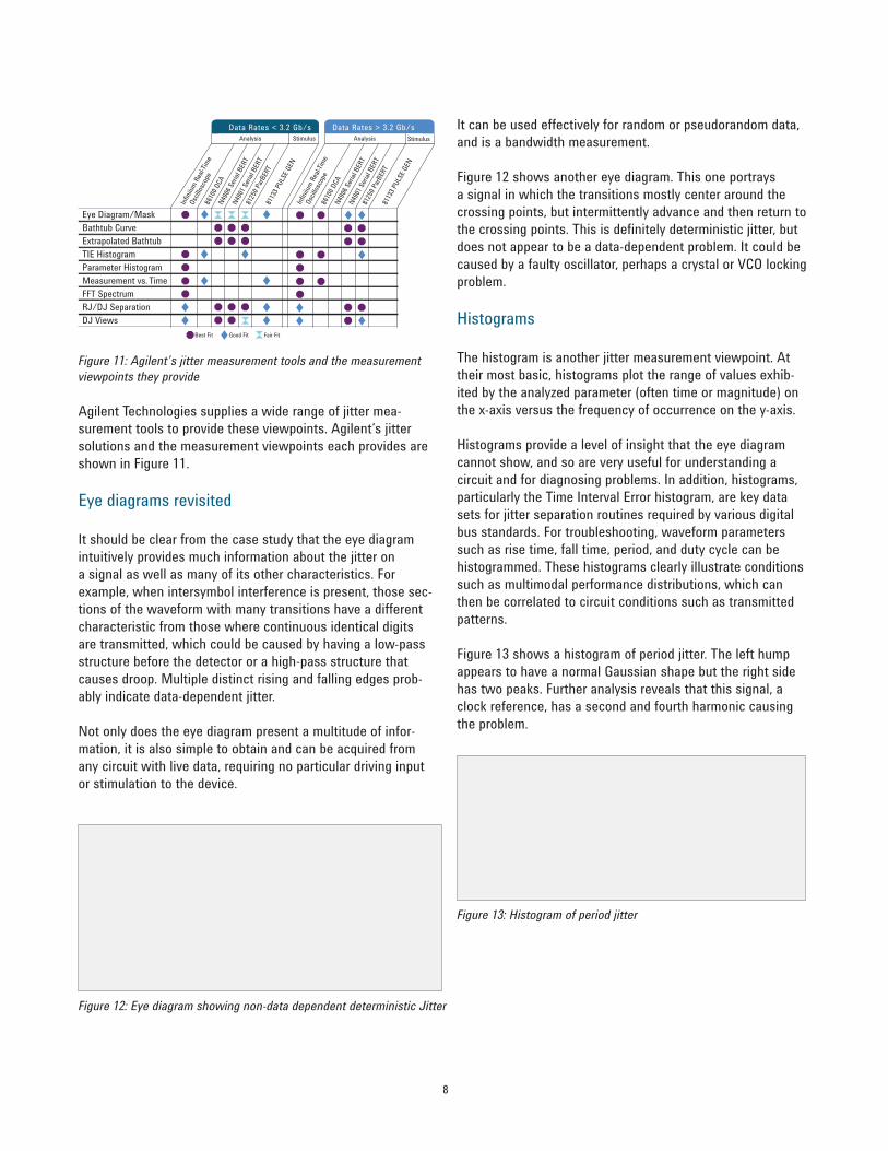
Figure 10: The same eye diagram showing all jittercomponents.
Finally for this case study, Figure 10 brings all the jitter components together as in the total jitter equation derived earlier. The deterministic component of the jitter on this waveform appears to be the most significant, and therefore the jitter component on which to concentrate jitter-reduction efforts, but again, this is a function of the persistence time used to capture the waveform. If the signal was captured for only a short time, then the actual random jitter could be much greater than it appears and would also be worthy of effort to reduce it.
Jitter measurement viewpoints
Now that jitter has been briefly described and explained, different ways to measure and view jitter can be examined. These various jitter measurement viewpoints can each pro-vide insight into the nature of the jitter affecting your system or device. Mentally integrating the different viewpoints can provide a more complete picture of the jitter, leading you to the jitter’s source and helping to identify ways to reduce or eliminate it. Jitter viewpoints range from the now-familiar eye diagram and histograms in the time domain, to frequency-domain analysis of jitter content, to views that allow separation of the random and deterministic components of the overall peak-to-peak jitter. Also included are methods for measuring a system’s response to jitter (jitter tolerance and jitter transfer).
8
Eye Diagram/MaskBathtub CurveExtrapolated BathtubTIE HistogramParameter HistogramMeasurement vs. TimeFFT SpectrumRJ/DJ SeparationDJ Views
8610
0 DCA
N490
6 Seri
al BE
RTN4
901 S
erial
BERT
8125
0 ParB
ERT
8113
3 PUL
SE G
EN
Analysis Stimulus
Infinii
um Re
al-Tim
e
Oscil
losco
pe
Infinii
um Re
al-Tim
e
Oscil
losco
pe
8610
0 DCA
N490
6 Seri
al BE
RTN4
901 S
erial
BERT
8125
0 ParB
ERT
8113
3 PUL
SE G
EN
Analysis Stimulus
Best Fit Good Fit Fair Fit
Data Rates < 3.2 Gb/s Data Rates > 3.2 Gb/s
Figure 11: Agilent’s jitter measurement tools and the measurement viewpoints they provide
Agilent Technologies supplies a wide range of jitter mea-surement tools to provide these viewpoints. Agilent’s jitter solutions and the measurement viewpoints each provides are shown in Figure 11.
Eye diagrams revisited
It should be clear from the case study that the eye diagram intuitively provides much information about the jitter on a signal as well as many of its other characteristics. For example, when intersymbol interference is present, those sec-tions of the waveform with many transitions have a different characteristic from those where continuous identical digits are transmitted, which could be caused by having a low-pass structure before the detector or a high-pass structure that causes droop. Multiple distinct rising and falling edges prob-ably indicate data-dependent jitter.
Not only does the eye diagram present a multitude of infor-mation, it is also simple to obtain and can be acquired from any circuit with live data, requiring no particular driving input or stimulation to the device.
UnitInterval
LeftCrossing
Point
RightCrossingPoint
Figure 12: Eye diagram showing non-data dependent deterministic Jitter
It can be used effectively for random or pseudorandom data, and is a bandwidth measurement.
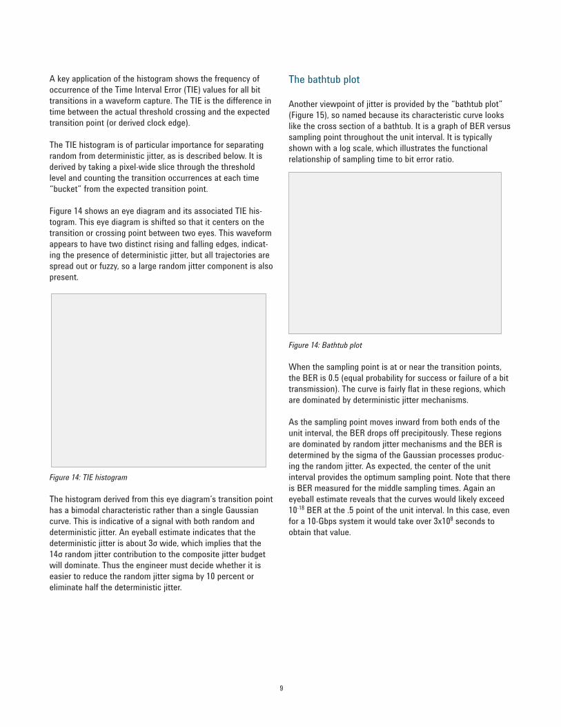
Figure 12 shows another eye diagram. This one portrays a signal in which the transitions mostly center around the crossing points, but intermittently advance and then return to the crossing points. This is definitely deterministic jitter, but does not appear to be a data-dependent problem. It could be caused by a faulty oscillator, perhaps a crystal or VCO locking problem.
Histograms
The histogram is another jitter measurement viewpoint. At their most basic, histograms plot the range of values exhib-ited by the analyzed parameter (often time or magnitude) on the x-axis versus the frequency of occurrence on the y-axis.
Histograms provide a level of insight that the eye diagram cannot show, and so are very useful for understanding a circuit and for diagnosing problems. In addition, histograms, particularly the Time Interval Error histogram, are key data sets for jitter separation routines required by various digital bus standards. For troubleshooting, waveform parameters such as rise time, fall time, period, and duty cycle can be histogrammed. These histograms clearly illustrate conditions such as multimodal performance distributions, which can then be correlated to circuit conditions such as transmitted patterns.
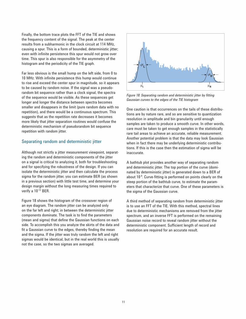
Figure 13 shows a histogram of period jitter. The left hump appears to have a normal Gaussian shape but the right side has two peaks. Further analysis reveals that this signal, a clock reference, has a second and fourth harmonic causing the problem.
Figure 13: Histogram of period jitter
9
A key application of the histogram shows the frequency of occurrence of the Time Interval Error (TIE) values for all bit transitions in a waveform capture. The TIE is the difference in time between the actual threshold crossing and the expected transition point (or derived clock edge).
The TIE histogram is of particular importance for separating random from deterministic jitter, as is described below. It is derived by taking a pixel-wide slice through the threshold level and counting the transition occurrences at each time “bucket” from the expected transition point.
Figure 14 shows an eye diagram and its associated TIE his-togram. This eye diagram is shifted so that it centers on the transition or crossing point between two eyes. This waveform appears to have two distinct rising and falling edges, indicat-ing the presence of deterministic jitter, but all trajectories are spread out or fuzzy, so a large random jitter component is also present.
Figure 14: TIE histogram
The histogram derived from this eye diagram’s transition point has a bimodal characteristic rather than a single Gaussian curve. This is indicative of a signal with both random and deterministic jitter. An eyeball estimate indicates that the deterministic jitter is about 3σ wide, which implies that the 14σ random jitter contribution to the composite jitter budget will dominate. Thus the engineer must decide whether it is easier to reduce the random jitter sigma by 10 percent or eliminate half the deterministic jitter.
The bathtub plot
Another viewpoint of jitter is provided by the “bathtub plot” (Figure 15), so named because its characteristic curve looks like the cross section of a bathtub. It is a graph of BER versus sampling point throughout the unit interval. It is typically shown with a log scale, which illustrates the functional relationship of sampling time to bit error ratio.
10
0.5
-3
10-6
10
BER
-9
10
0 L RBT DJ T DJ0.5T BT
-12
Dete
rmin
istic
Dete
rmin
istic
Rand
om
Rand
om
Figure 14: Bathtub plot
When the sampling point is at or near the transition points, the BER is 0.5 (equal probability for success or failure of a bit transmission). The curve is fairly flat in these regions, which are dominated by deterministic jitter mechanisms.
As the sampling point moves inward from both ends of the unit interval, the BER drops off precipitously. These regions are dominated by random jitter mechanisms and the BER is determined by the sigma of the Gaussian processes produc-ing the random jitter. As expected, the center of the unit interval provides the optimum sampling point. Note that there is BER measured for the middle sampling times. Again an eyeball estimate reveals that the curves would likely exceed 10-18 BER at the .5 point of the unit interval. In this case, even for a 10-Gbps system it would take over 3x10⁸ seconds to obtain that value.

10
The curves of the bathtub plot readily show the transmission- error margins at the BER level of interest. The further the left edge is from the right edge at a specified BER (again, 10-12 is commonly used), the more margin the design has to jitter, and of course, the closer these edges become, the less margin is available. These edges are directly related to the tails of the Gaussian functions derived from TIE histograms. The bathtub plot can also be used to separate random and deterministic jitter and determine the sigma of the random component, asdescribed below.
Frequency-domain jitter views
Viewing jitter in the frequency domain is yet another way to analyze its sources. Deterministic jitter sources appear as line spectra in the frequency domain. This frequency-domain view is provided by phase noise or jitter spectrum analysis, and relates phase noise or jitter versus frequency offset from a carrier or clock.
Phase-noise measurements yield the most accurate apprais-als of jitter due to effective oversampling and bandwidth control in measurement. They provide invaluable insights into a design, particularly for phase locked loop or crystal oscil-lator designs, and readily identify deterministic jitter due to spurs. They are helpful for optimizing clock recovery circuits and discovering internal generators of spurs and noise.
Phase-noise measurements can also be integrated over a specific bandwidth to yield total integrated jitter, although this is not directly convertible to peak-to-peak jitter as specified for data communications standards. Figure 16 shows an intrinsic jitter spectrum of a phase locked loop.
DeterministicSources
Noise Peaking
Figure 16: Intrinsic jitter spectrum
Noise peaking occurs at a 2-kHz offset. There are also frequency lines that identify deterministic jitter sources. The frequency lines ranging from 60 Hz to about 800 Hz are power-line spurs. Frequency lines evident in the range of 2 to 7 MHz are most likely clock reference-induced spurs, again causing deterministic jitter.
Another method of obtaining a frequency-domain viewpoint of jitter is to take an FFT of the Time Interval Error data. The FFT has much less resolution than the low-level phase noise view, but is an excellent method of viewing high-level phenomena quickly and easily.
Figure 17 shows a number of views of the same signal, a 456-MHz clock signal as shown on the top trace. The second line shows the histogram of a transition point. This histogram is obviously not Gaussian, indicating the presence of deterministic as well as random jitter on the signal. The third line plots Time Interval Error versus time; ideally with no jitter this would be a straight line. If this signal were a data signal rather than a clock signal, it would be possible to correlate data patterns to the TIE. For instance, if every time a 0010 sequence appeared on the data trace the TIE was posi-tive, some sort of data-dependent jitter would be indicated.
Figure 14: Several views of a 456-MHz clock signal (A), including, a histogram of a transition point (B), TIE versus time (C), and an FFT of the TIE data (D).
11
Finally, the bottom trace plots the FFT of the TIE and shows the frequency content of the signal. The peak at the center results from a subharmonic in the clock circuit at 114 MHz, causing a spur. This is a form of bounded, deterministic jitter; even with infinite persistence this spur would not grow over time. This spur is also responsible for the asymmetry of the histogram and the periodicity of the TIE graph.
Far less obvious is the small hump on the left side, from 0 to 10 MHz. With infinite persistence this hump would continue to rise and exceed the center spur in magnitude, so it appears to be caused by random noise. If the signal was a pseudo-random bit sequence rather than a clock signal, the spectra of the sequence would be visible. As these sequences get longer and longer the distance between spectra becomes smaller and disappears in the limit (pure random data with no repetition), and there would be a continuous spectrum. This suggests that as the repetition rate decreases it becomes more likely that jitter separation routines would confuse the deterministic mechanism of pseudorandom bit sequence repetition with random jitter.
Separating random and deterministic jitter
Although not strictly a jitter measurement viewpoint, separat-ing the random and deterministic components of the jitter on a signal is critical to analyzing it, both for troubleshooting and for specifying the robustness of the design. If you can isolate the deterministic jitter and then calculate the process sigma for the random jitter, you can estimate BER (as shown in a previous section) with little test time, and determine your design margin without the long measuring times required to verify a 10-12 BER.
Figure 18 shows the histogram of the crossover region of an eye diagram. The random jitter can be analyzed only on the far left and right; in between the deterministic jitter components dominate. The task is to find the parameters (mean and sigma) that define the Gaussian functions on each side. To accomplish this you analyze the skirts of the data and fit a Gaussian curve to the edges, thereby finding the mean and the sigma. If the jitter was truly random the left and right sigmas would be identical, but in the real world this is usually not the case, so the two sigmas are averaged.
Figure 18: Separating random and deterministic jitter by fitting Gaussian curves to the edges of the TIE histogram
One caution is that occurrences on the tails of these distribu-tions are by nature rare, and so are sensitive to quantization resolution in amplitude and bin granularity until enough samples are taken to produce a smooth curve. In other words, care must be taken to get enough samples in the statistically rare tail areas to achieve an accurate, reliable measurement. Another potential problem is that the data may look Gaussian when in fact there may be underlying deterministic contribu-tions. If this is the case then the estimation of sigma will be inaccurate.
A bathtub plot provides another way of separating random and deterministic jitter. The top portion of the curve (domi-nated by deterministic jitter) is generated down to a BER of about 10-9. Curve-fitting is performed on points clearly on the steep portion of the bathtub curve, to estimate the param-eters that characterize that curve. One of these parameters is the sigma of the Gaussian curve.
A third method of separating random from deterministic jitter is to use an FFT of the TIE. With this method, spectral lines due to deterministic mechanisms are removed from the jitter spectrum, and an inverse FFT is performed on the remaining Gaussian noise record to reveal random jitter without the deterministic component. Sufficient length of record and resolution are required for an accurate result.
12
Jitter tolerance and jitter transfer
Not included in the list of viewpoints (Figure 11) but impor-tant nonetheless are two measurements that don’t actually measure jitter itself, but rather measure a device’s response to jitter. They are also different in that they require a mea-sured stimulus input to the device, rather than just passively measuring an output or other signal.
Jitter Tolerance is a measure of how a known amount of input jitter affects the BER of a device. In the SONet and SDH specifications, this is defined with a specific algorithm, but it is a useful characterization for other systems as well. The measurement sequence requires an instrument such as a pat-tern generator that can supply a signal with precise amounts of jitter (usually sinusoidal), and also a means to measure raw bit error ratio on the output. The test provides insight into how well the DUT’s clock recovery circuits or phase locked loop responds to jitter.
Figure 19 shows a plot of UI jitter amplitude versus frequency that results in an equivalent 1-dB reduction in sensitivity after the signal level is adjusted 1 dB higher than that required to establish a given BER (10-12). The solid line shown is a specification mask that presents the minimum acceptable jitter tolerance levels.
10
10 102
Modulation Frequency (Hz)
Ampl
itude
(UI)
103 104 105 106 107
1
0.1
Figure 19: Jitter Tolerance test results
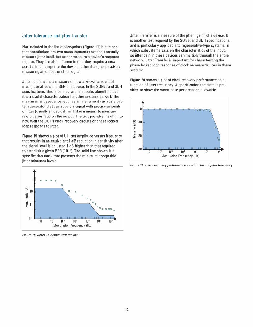
Jitter Transfer is a measure of the jitter “gain” of a device. It is another test required by the SONet and SDH specifications, and is particularly applicable to regenerative-type systems, in which subsystems pass on the characteristics of the input, so jitter gain in these devices can multiply through the entire network. Jitter Transfer is important for characterizing the phase locked loop response of clock recovery devices in these systems.
Figure 20 shows a plot of clock recovery performance as a function of jitter frequency. A specification template is pro-vided to show the worst-case performance allowable.
-10
0
10 102
Modulation Frequency (Hz)
Tran
sfer
(dB)
103 104 105 106 107
-20
-30
Figure 20: Clock recovery performance as a function of jitter frequency

13
After various viewpoints for evaluating jitter are understood, it is necessary to evaluate the tools required to obtain these viewpoints. Before determining your tool requirements, you need to consider the types of tests you will be conducting, the characteristics of the devices you will be testing, and also the testing environment. Some tools may be more appropriate for the R&D environment while others have advantages in speed and cost per test and are therefore more useful in the manufacturing environment. The data rate of the devices you will be testing also limits your tool choices.
The types of instruments relevant to jitter evaluation can be grouped into instruments providing stimulus and those provid-ing jitter measurement and analysis.
Pulse/pattern generator
The pulse/pattern generator is the primary instrument in the stimulus category. A bit error ratio tester (BERT) can also provide input stimulus to a DUT and is discussed with jitter analysis tools.
Pulse/pattern generators must be able to create arbitrary patterns in either differential or single-ended structures, with a minimum of phase noise. They allow selection of pseudo-random structures to emulate random data; the lengths of these structures can range from bits to megabits. They also have a jitter or delay control to allow you to set up a pattern with a precise amount of jitter, enabling you to characterize your circuit’s response to it, as is required for jitter tolerance and jitter transfer testing.
Figure 21: Agilent 81150A pulse/pattern generator
Low-level phase-noise/spectrum analyzer
Several instruments are needed to provide the variety of jitter viewpoints to obtain a comprehensive picture of the jitter affecting your device or system. A phase-noise or low-level jitter analysis system is necessary to obtain an intrinsic jitter spectrum. These instruments provide the highest level of accuracy in measuring the frequency content of the jitter in your design. They derive their accuracy from a high degree of oversampling and a narrow measurement bandwidth, and will uncover deterministic jitter mechanisms not detected by oscilloscopes. These systems exhibit extremely low noise floors and must be immune to amplitude noise, which is one reason why phase-noise systems are preferred for this purpose over spectrum analyzers.
Low-level jitter analysis can be used as a design or trouble-shooting aid when examining noise-floor mechanisms, phase locked loops, VCOs, crystal oscillators, and other clocks and references, areas in which random jitter needs to be carefully monitored. Using a precision system based on frequency-domain phase measurement techniques is critical for this type of analysis.
Spectral evaluation often leads to great insights into design and system idiosyncrasies not observable by other techniques. However, low-level analysis is limited to jitter components less than 200 MHz, substantially below the full bandwidth many standards stipulate, so other jitter analysis tools are also required for spectral analysis requiring greater bandwidth.
Figure 22: Agilent JS-1000 low-level phase noise/spectrum analyzer
14
Real-time sampling oscilloscopes
High-speed real-time digital storage oscilloscopes (DSOs) are the most versatile, flexible, and commonly used instruments for jitter analysis. A rule of thumb is that the bandwidth of analysis should be at least 1.8 times the maximum bit rate for a non-return-to-zero (NRZ) serial signal. Real-time oscil-loscopes now have bandwidths in excess of 60 GHz and jitter measurements floors below 100 fs.
DSOs oversample a signal at least 2 times and sometimes more than 3.5 times the maximum bandwidth possible in order to capture the entire signal in a single acquisition. They may interpolate between these samples to increase the effective time resolution of a waveform capture. Oversampling oscilloscopes acquire a signal in about a tenth of the time of undersampling oscilloscopes (such as digital communications analyzers), but are considered slow compared to a BERT with respect to appraising edge-to-edge metrics.
You can route signals directly to an oscilloscope or tap an active circuit using high-bandwidth probes. Care must be taken to select and use probes correctly, as these are often the weakest link in a data acquisition setup.
After a waveform is captured, many measurement and display functions can be employed such as producing eye diagrams, recovering the transmitter clock, and determining Time Interval Error, duty-cycle, rise-time, and fall-time parameters. Oscilloscopes can display histograms and trend lines for any of these parameters, and perform FFTs to determine fre-quency content of the data. They can obtain a variety of jitter parameters such as cycle to cycle, n cycle, period, and delay, and can simultaneously display the data waveform, time-trend data, and the FFT of these measurements (as shown in Figure 17), giving great diagnostic abilities.
Oscilloscopes can also be used in conjunction with jitter analysis software to provide further capabilities such asrandom/deterministic jitter separation, and to tailor the measurements to specific standards.
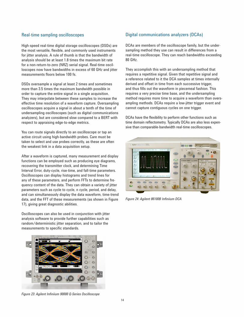
Figure 23: Agilent Infiniium 90000 Q-Series Oscilloscope
Digital communications analyzers (DCAs)
DCAs are members of the oscilloscope family, but the under-sampling method they use can result in differences from a real-time oscilloscope. They can reach bandwidths exceeding 80 GHz.
They accomplish this with an undersampling method that requires a repetitive signal. Given that repetitive signal and a reference related to it the DCA samples at times internally derived and offset in time from each successive trigger, and thus fills out the waveform in piecemeal fashion. This requires a very precise time base, and the undersampling method requires more time to acquire a waveform than overs-ampling methods. DCAs require a low-jitter trigger event and cannot capture contiguous cycles on one trigger.
DCAs have the flexibility to perform other functions such as time domain reflectometry. Typically DCAs are also less expen-sive than comparable-bandwidth real-time oscilloscopes.
Figure 24: Agilent 86100B Infiniium DCA

15
Bit error ratio testers (BERTs)
Bit error ratio is a key performance metric in digital com-munications designs, and BERTs play a significant role in testing these systems. They provide comprehensive stimulus/response testing, but can also perform stimulus-only and response-only functions. BERTs provide solutions up to 45 Gbps and come in different configurations: serial only, serial to parallel, parallel to serial, and parallel to parallel. These configurations allow them to test a wide variety of dif-ferent systems, a good example being serializer to deserializer (SERDES) modules. BERTs count every edge or transition on a waveform, so provide the fastest measurement on a per-transition basis.
BERTs allow adjustment of the sample-time location and the threshold levels. These features are useful for generating point eye diagrams and iso-BER diagrams (with contour lines delimiting equal probability areas in the eye diagram). BERT tools enable bathtub plot creation, bathtub plot extrapolation (which speeds the creation of bathtub plots), and random/deterministic jitter separation.
Figure 25: Agilent N4906A Series BERT
Logic analyzers with EyeScan
Logic analyzers are usually not considered for obtaining parametric measurements or studying jitter. However, when equipped with a feature called EyeScan, they can monitor every edge of up to 300 parallel lines simultaneously on systems up to 1.5 Gbps, and so are ideal for analyzing skew on parallel buses. EyeScan can provide measurements with 10 ps of resolution. If a trace exhibits excessive skew or eye closure, the user interface allows you to activate that trace independently to focus in on it.
Choose your tools wisely
Agilent Technologies can supply all the tools you need to study jitter in the digital systems you design. As systems continue to become faster and more complex, maintaining signal integrity will become an increasingly important part of assessing digital designs, and will be necessary to meet the ever decreasing product cycle times.
References
Agilent Jitter Solutionswww.agilent.com/find/jitter
Signal Integrity Application Informationwww.agilent.com/find/si
Eye Diagram/MaskBathtub CurveExtrapolated BathtubTIE HistogramParameter HistogramMeasurement vs. TimeFFT SpectrumRJ/DJ SeparationDJ Views
Infinii
um Re
al-Tim
e
Oscil
losco
pe
Infinii
um Re
al-Tim
e
Oscil
losco
pe
8610
0 DCA
N490
6 Seri
al BE
RTN4
901 S
erial
BERT
8125
0 ParB
ERT
8113
3 PUL
SE G
EN
Analysis Stimulus
8610
0 DCA
N490
6 Seri
al BE
RTN4
901 S
erial
BERT
8125
0 ParB
ERT
8113
3 PUL
SE G
EN
Analysis Stimulus
Best Fit Good Fit Fair Fit
Data Rates < 3.2 Gb/s Data Rates > 3.2 Gb/s
Figure 26: Agilent 16900B Logic Analyzer and EyeScan

www.lxistandard.org LAN eXtensions for Instruments puts the power of Ethernet and the Web inside your test systems. Agilent is a founding member of the LXI consortium.
Agilent Channel Partnerswww.agilent.com/find/channelpartnersGet the best of both worlds: Agilent’s measurement expertise and product breadth, combined with channel partner convenience.
For more information on Agilent Technologies’ products, applications or services, please contact your local Agilent office. The complete list is available at:www.agilent.com/find/contactus
Americas Canada (877) 894 4414 Brazil (11) 4197 3600Mexico 01800 5064 800 United States (800) 829 4444
Asia Pacific Australia 1 800 629 485China 800 810 0189Hong Kong 800 938 693India 1 800 112 929Japan 0120 (421) 345Korea 080 769 0800Malaysia 1 800 888 848Singapore 1 800 375 8100Taiwan 0800 047 866Other AP Countries (65) 375 8100
Europe & Middle EastBelgium 32 (0) 2 404 93 40 Denmark 45 45 80 12 15Finland 358 (0) 10 855 2100France 0825 010 700* *0.125 €/minuteGermany 49 (0) 7031 464 6333 Ireland 1890 924 204Israel 972-3-9288-504/544Italy 39 02 92 60 8484Netherlands 31 (0) 20 547 2111Spain 34 (91) 631 3300Sweden 0200-88 22 55United Kingdom 44 (0) 118 927 6201For other unlisted countries: www.agilent.com/find/contactus(BP-3-1-13)
Product specifications and descriptions in this document subject to change without notice.
© Agilent Technologies, Inc. 2013Published in USA, September 16, 20135988-9109EN
www.agilent.com
www.agilent.com/quality
www.axiestandard.org AdvancedTCA® Extensions for Instrumentation and Test (AXIe) is an open standard that extends the AdvancedTCA for general purpose and semiconductor test. Agilent is a founding member of the AXIe consortium.
www.pxisa.org PCI eXtensions for Instrumentation (PXI) modular instrumentation delivers a rugged, PC-based high-performance measurement and automation system.
Quality Management SystemQuality Management SysISO 9001:2008Agilent Electronic Measurement Group
DEKRA Certified
www.agilent.com/find/myagilent A personalized view into the information most relevant to you.
myAgilentmyAgilent
www.agilent.com/find/AdvantageServicesAccurate measurements throughout the life of your instruments.
Agilent Advantage Services
Three-Year Warranty
www.agilent.com/find/ThreeYearWarrantyAgilent’s combination of product reliability and three-year warranty coverage is another way we help you achieve your business goals: increased confidence in uptime, reduced cost of ownership and greater convenience.