measurement and characterization of euv mask performance ...€¦ · measurement and...
TRANSCRIPT

Measurement and characterization of EUV mask
performance at high-NA
Rikon ChaoAndrew R. Neureuther, Ed.Laura Waller, Ed.Patrick Naulleau, Ed.
Electrical Engineering and Computer SciencesUniversity of California at Berkeley
Technical Report No. UCB/EECS-2013-56
http://www.eecs.berkeley.edu/Pubs/TechRpts/2013/EECS-2013-56.html
May 10, 2013

Copyright © 2013, by the author(s).All rights reserved.
Permission to make digital or hard copies of all or part of this work forpersonal or classroom use is granted without fee provided that copies arenot made or distributed for profit or commercial advantage and that copiesbear this notice and the full citation on the first page. To copy otherwise, torepublish, to post on servers or to redistribute to lists, requires prior specificpermission.

Measurement and characterization of EUV mask performance at high-NA by Rikon Chao
Research Project
Submitted to the Department of Electrical Engineering and Computer Sciences, University of California at Berkeley, in partial satisfaction of the requirements for the degree of Master of Science, Plan II. Approval for the Report and Comprehensive Examination:
Committee:
Professor Andrew Neureuther Research Advisor
(Date)
* * * * * * *
Professor Laura Waller Second Reader
(Date)
* * * * * * *
Doctor Patrick Naulleau Third Reader
(Date)

1
ABSTRACT In this work, we used a high accuracy synchrotron-based reflectometer to experimentally determine the effects of angular bandwidth limitations on high-NA EUV mask performance. We collected the scatterometry data of both the mask blank and absorber field, as well as mask pattern diffraction performance as a function of illumination angle, scatter angle, and wavelength. Gratings down to 44 nm half pitch on mask, up to 16° angle of incidence (AOI), and wavelength ranging from 13.3 to 13.7 nm were considered. Rigorous Coupled-Wave Analysis (RCWA) was used to model scatterometry results which were compared with measurement. The experimental measurements on a mask with a multilayer reflectivity of over 60% at 13.5 nm wavelength that peaked about 10° showed that computing the large area reflectivity as a function of wavelength and incident angle from 0 to 14° resulted in root mean square errors in reflectivity unacceptably as high as 13% and 0.8% of the incident beam for the multilayer and absorber respectively. This dropped to 5% and 0.7% respectively when interdiffusion and wavelength-dependent refractive indices were taken into account. Calibration by fitting to the measured data reduced the errors to 0.8% and 0.08% respectively. Measurements of patterned gratings compared to a simple binary mask with 60% clear-field energy transmission for a 176 nm pitch grating showed less zero order than expected and an imbalance the two first orders where one exceeded the simple binary mask prediction. The levels of these orders degraded further for smaller pitches at 88 nm and especially at large incident angles of 14° where diffracted orders had large angles compared to the angular bandwidth of the multilayer. Fortunately, RCWA-based modeling of the patterned mask assuming the simplest case of vertical absorber walls predicted a similar trend in the diffraction to that observed from the measurement.

2
ACKNOWLEDGEMENT I am deeply grateful to my advisors, Professor Andrew Neureuther and Dr. Patrick Naulleau, for their relentless support and motivation. Andy has always encouraged me and provided me with resources and valuable suggestions. Even in his retirement, he enjoys having meetings with the group while sharing pictures of some of the most beautiful creatures in the world that he took in the backcountry. Every single meeting with him has been enjoyable and fruitful. Patrick was always there whenever I needed help or was confused how I should move forward. He never failed to answer my questions and I have been impressed by how responsive he has been. From recommendation letter to connections to the industry, he has assisted me to make my graduate life smoother. I would also like to thank Professor Laura Waller for being the second reviewer of my report, and for her knowledgeable and inspiring class which had helped my research. I am thankful to Dr. Ryan Miyakawa, who helped me accustomed to not only our working environment at Lawrence Lab, but also a graduate student life in the US. I am thankful to Eric Gullikson for the discussion of the experiments and the theories behind them with me. This report could not have been completed without Eric’s help. I also thank Rene Claus and Suchit Bhattarai for inspiring and clever ideas. I would like to acknowledge the financial support of my graduate career, which was funded by Intel. I especially thank Ted Liang for his support on my projects. The software support was provided by Tom Pistor of Panoramic Technologies. This work was supported in part by Zeiss and Samsung and carried out at Lawrence Berkeley National Laboratory which is operated under the auspices of the Director, Office of Science, of the U.S. Department of Energy under Contract No. DE-AC02-05CH11231.

3
Chapter 1
INTRODUCTION In order to meet future scaling requirements on integrated circuit feature sizes, the numerical aperture in extreme ultraviolet (EUV) lithography system is expected to be extended to 0.45 or beyond. The reflective nature of EUV masks, however, requires the angle of incidence (AOI) to be higher than what is currently being used if high NA systems are adopted. Assuming a magnification of 4x would require a mean illumination angle of 9° at the mask. If an AOI of 9° is used with a partial coherence of unity, and an NA of 0.5, the maximum AOI encountered is
𝐴𝑂𝐼𝑚𝑎𝑥 = 9 + sin−10.54 = 16.2
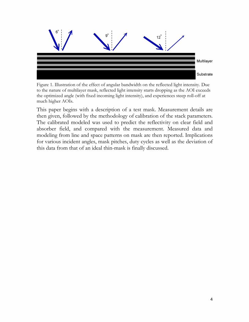
At such a high incident angle, there are two effects limiting the performance of an EUV mask, angular bandwidth and mask shadowing. The former effect describes the dropping of reflectivity at incident angle far beyond the optimized angle as shown in Figure 1. The mask designed for this work was optimized at 6° AOI. This can be compensated for by sacrificing reflectivity at lower angles, with a different design of the broadband multilayer stack [1]. The latter effect, mask shadowing, can in theory be mitigated by thinning the absorber layer [2], but this would in turn be limited by the absorption performance. Simulation work showed that it is possible to have either good imaging contrast or reasonable efficiency, but not both [3]. This drove the authors of [3] to the conclusion that a higher NA (>>0.33) is only possible if accompanied by an increased demagnification in order to reduce the AOI at the reticle. It thus becomes important to experimentally determine how the limitations affect the diffraction performance.
4
Figure 1. Illustration of the effect of angular bandwidth on the reflected light intensity. Due to the nature of multilayer mask, reflected light intensity starts dropping as the AOI exceeds the optimized angle (with fixed incoming light intensity), and experiences steep roll-off at much higher AOIs. This paper begins with a description of a test mask. Measurement details are then given, followed by the methodology of calibration of the stack parameters. The calibrated modeled was used to predict the reflectivity on clear field and absorber field, and compared with the measurement. Measured data and modeling from line and space patterns on mask are then reported. Implications for various incident angles, mask pitches, duty cycles as well as the deviation of this data from that of an ideal thin-mask is finally discussed.
5
Chapter 2
MASK DESIGN AND MEASUREMENT 2.1 Mask layout
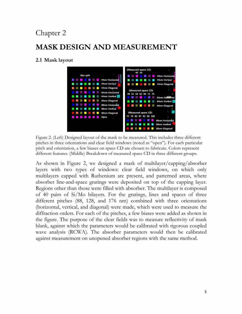
Figure 2. (Left) Designed layout of the mask to be measured. This includes three different pitches in three orientations and clear field windows (noted as “open”). For each particular pitch and orientation, a few biases on space CD are chosen to fabricate. Colors represent different features. (Middle) Breakdown of measured space CD in three different groups.
As shown in Figure 2, we designed a mask of multilayer/capping/absorber layers with two types of windows: clear field windows, on which only multilayers capped with Ruthenium are present, and patterned areas, where absorber line-and-space gratings were deposited on top of the capping layer. Regions other than those were filled with absorber. The multilayer is composed of 40 pairs of Si/Mo bilayers. For the gratings, lines and spaces of three different pitches (88, 128, and 176 nm) combined with three orientations (horizontal, vertical, and diagonal) were made, which were used to measure the diffraction orders. For each of the pitches, a few biases were added as shown in the figure. The purpose of the clear fields was to measure reflectivity of mask blank, against which the parameters would be calibrated with rigorous coupled wave analysis (RCWA). The absorber parameters would then be calibrated against measurement on unopened absorber regions with the same method.

6
2.2 Measurement Reflectivity and scattering measurements were performed using the synchrotron-based reflectometer of the Calibrations and Standards Beamline 6.3.2 at Advanced Light Source (ALS), Lawrence Berkeley National Laboratory (LBNL). The beamline has a high spectral purity of 99.98%, wavelength precision of 0.007%, and a reflectance precision of 0.08% [4]. Reflectivity on clear field and absorber field was measured at angles of incidence (AOI) of 2°, 4°, 6°, 8°, 9°, 10°, 12°, 14°, and 16°, and the wavelength spanned from 13.3 nm to 13.7 nm with steps of 0.05 nm. Detector angles were set at the same angles as AOI, except on the other side, as shown in Figure 3. For scattering measurements, data was collected at the same set of AOI and wavelengths, except the detector was positioned at angles where scattered orders occur. The measurement was done on 8 chosen vertical grating windows (space CD/pitch): 40/88, 44/88, 58/128, 62/128, 66/128, 83/176, 87/176, and 92/176. The angles of detector θd for any combination of wavelength λ, pitch d, and AOI θi, at nth order, were precalculated using
𝑛𝜆 = 𝑑(𝑠𝑖𝑛𝜃𝑑 − 𝑠𝑖𝑛𝜃𝑖) Scattered data was collected up to 45° on either side from specular, unless overlapping with incidence. See Figure 4.

7
Figure 3. During the measurement of reflectivity on clear field multilayer, the source was positioned at AOI of 2°, 4°, 6°, 8°, 9°, 10°, 12°, 14°, and 16°. The detector on the other side followed the same AOI as the incidence. The reflectivity was measured as the ratio of detected light intensity to incident light intensity.
Figure 4. For measurement on absorber gratings, the light source was positioned at fixed AOI of 2°, 4°, 6°, 8°, 9°, 10°, 12°, 14°, and 16°. The detector scanned through angles at which the diffraction took place.

8
Chapter 3
THIN-FILM MODEL 3.1 Calibration of parameters with optimization algorithm The modeling work of clear field reflectivity was conducted using rigorous coupled-wave analysis (RCWA) in HyperLith [5] supported by Panoramic Technology, Inc. The tool simulated 1) the aerial image of 3D multilayer stack model given multilayer materials, thicknesses, and refractive indices of the layers, and calculated the reflectivity of the multilayer; and 2) the diffraction orders caused by the absorber line patterns given the absorber and buffer layer materials and their properties. Initial parameters in this modeling work include pitch of Si/Mo multilayer, γ (ratio of Mo thickness over pitch), Ru (as capping layer) thickness, and refractive indices for Si, Mo, and Ru. It is known that interdiffusion takes place at the Si/Mo interfaces and degrades the reflectivity performance [6]. To account for the interdiffusion effects between various layers, we added MoSi2 at every Mo/Si interface in the modeling [7], and Ru2Si3 at Ru/Si interface [8]. Due to possibly different amount of interdiffusion formed by the top and bottom Si and Mo, we set them as different fitting parameters. Another consideration we included is the dependency of n and k on the wavelength. Also, since phase roughness replicated through the multilayer can be another source of reflectivity reduction, we added a scaling factor as an additional fitting parameter that scaled down the modeling data to have a better fit with measured data. With the support of Panoramic API, we set up automated optimization routine to calibrate the values of the parameters that would give best fit to the measured reflectivity data. Table 1 shows the measured thicknesses and refractive indices, based on which each of the parameters was assigned an initial value and a range within which it was allowed to float, as shown in Table 2. Some initial values not measured and recorded in Table 1 such as interdiffusion thicknesses were found by preliminary manual search. N and k values were corrected for different wavelengths according to differences calculated from the CXRO database [9]. We fit the clear field reflectivity first, followed by fitting of absorber field reflectivity. We hoped to find a set of parameters that best predict the measured data in terms of minimum errors.

9
Layer (from top)
1 2 3 Multilayer
Material Absorber Buffer Capping Si/Mo Thickness
(target) 14 nm 56 nm 2.5 nm
40 pairs, Period=7nm, gamma=0.4 (approx.)
n (13.5 nm) 0.9556 0.9492 0.9026 Si (top)=0.99901, Mo (bottom)=0.921838 k (13.5 nm) 0.0232 0.0296 0.0157 Si (top)=0.001826, Mo (bottom)=0.006334
Remarks Measured @CXRO
Measured @CXRO
Measured @CXRO
CXRO database
Table 1. Mask stack info measured at Center of X-Ray Optics (CXRO), LBNL or taken from CXRO database [9]
Parameter Initial Value
Lower Bound
Upper Bound
Final Source of n and k values
Scaling factor 1 0.83 1 0.9983 - Absorber thickness (nm) 14 14*0.5 14*2 28
Measured at CXRO
Buffer thickness (nm) 56 56*0.5 56*2 57.09
Ru thickness, clear field (nm) 1.75 0 See
remark 1 4.65
Ru thickness, absorber field (nm) 1.75 See
remark 1 - 4.94
Ru2Si3 thickness 1 0 - 0.02
CXRO database
Top Si thickness (nm) 2.73 0 Pitch 2.85 MoSi2 (above Mo) thickness (nm) 1.37 0 Pitch 1.53
Mo Thickness (nm) 1.81 0 Pitch 1.82 MoSi2 (above Si) thickness (nm) 1.09 0 Pitch 1.00
Si thickness (nm) 2.73 0 Pitch 2.65 Bottom Mo thickness (nm) 1.81 0 Pitch 2.33
Remark 1: Due to possible overetching, Ru thickness on clear field can only be smaller than that on absorber field. Table 2. List of parameters used in the optimization routine with respective ranges and the final value we arrived at to predict the diffraction.

10
3.2 Comparison of measured and modeled reflectivity The final values that the routine arrived at gave a prediction of clear field reflectivity at various AOI as shown in the modeled curves in Figure 5, where measured curves are present for comparison. In these curves, we observed angular bandwidth nature of EUV reflective masks: the reflectivity of EUV light could not be high throughout the angles of interest. It was needed to optimize the mask to provide good reflectivity at a certain AOI, which inevitably sacrificed the performance at higher angles. The subplots in Figure 5 showed reflectivity at different wavelengths, and it was apparent that reflectivity at a certain AOI was highly dependent on wavelengths. Figure 6 shows the results when the absorber was added, and did not have as good performance as what are seen in Figure 5. Two parameters that arrived at a value much further than expected were Ru and absorber thicknesses, which ended up being ~ 2 nm more and twice as much (stopped by the upper bound) than the measurement, respectively. Interdiffusion between Ru and top Si layer came to a negligible value. Other values stayed closed to what was suggested initially. To compare the improvement on the model, the root mean square errors (RMSE) was defined as the following:
𝑅𝑀𝑆𝐸𝑐𝑙𝑟 = �∑ [(𝑚𝑜𝑑𝑒𝑙𝑒𝑑𝑐𝑙𝑒𝑎𝑟(𝐴𝑂𝐼, 𝜆) ∙ 𝑠𝑐𝑎𝑙𝑖𝑛𝑔 −𝑚𝑒𝑎𝑠𝑢𝑟𝑒𝑑𝑐𝑙𝑒𝑎𝑟(𝐴𝑂𝐼, 𝜆))2]𝐴𝑂𝐼,𝜆
𝑁𝑐𝑙𝑒𝑎𝑟 × 100%
𝑅𝑀𝑆𝐸𝑎𝑏𝑠 = �∑ [(𝑚𝑜𝑑𝑒𝑙𝑒𝑑𝑎𝑏𝑠𝑜𝑟𝑏𝑒𝑟(𝐴𝑂𝐼, 𝜆) ∙ 𝑠𝑐𝑎𝑙𝑖𝑛𝑔 − 𝑚𝑒𝑎𝑠𝑢𝑟𝑒𝑑𝑎𝑏𝑠𝑜𝑟𝑏𝑒𝑟(𝐴𝑂𝐼, 𝜆))2]𝐴𝑂𝐼,𝜆
𝑁𝑎𝑏𝑠𝑜𝑟𝑏𝑒𝑟 × 100%
Using the stack info data from Table 1, the simplest model, the simulation yielded RMSEclr and RMSEabs of 13.18%, and 0.771% respectively. When interdiffusion and wavelength-dependent refractive indices were taken into account with the initial values suggested in Table 2, RMSEclr and RMSEabs have dropped to 4.74% and 0.701% respectively. After calibration on the parameters, RMSEclr, and RMSEabs arrived at 0.8% and 0.08% respectively. This showed a significant improvement in error reduction. This ensured the following diffraction modeling could have as little error resulting from the inaccuracy of parameters as possible.

11
Figure 5. Clear field reflectivity of measured and modeled data. Modeling parameters are optimized for best fit to clear field based on minimum error. The horizontal axis (Angle from glancing) is the complementary angle of incidence.

12
Figure 6. Absorber field reflectivity of measured and modeled data. Si/Mo stack parameters are optimized for clear field, while absorber and buffer layer parameters are optimized for absorber field based on minimum error.

13
Chapter 4
DIFFRACTION DATA 4.1 Grating diffraction orders modeling compared with measurement Based on the calibrated values we considered best representing the mask stack, we modeled the diffraction orders as a function of AOI, wavelength, space CDs and pitches. The model assumes the sidewalls to be perfectly vertical, with no line edge roughness. This might contribute to the errors observed in the diffraction orders between modeled and measured data. Some of the results are shown in Figure 7. As the light is coming from an oblique angle, from the plots in Figure 7 we can clearly see that the intensities are not symmetrical about the 0th order. However, at larger pitches and smaller AOI, the diffraction intensities show a more symmetrical profile. This is expected, both due to reduced shadowing effects and the smaller angular bandwidth of the diffraction pattern. Note that the effect is also exacerbated by the fact that the multilayer is designed for an angle of incidence of 6°. In principle, one could readily optimize the multilayer d-spacing to match the AOI; however, as discussed above, increasing multilayer angular bandwidth is more complicated and will come at the cost of flux. Table 3 gives the measured intensity at -2nd to 2nd orders for selected combination of pitches and AOI. Since the grating 87/176 has a duty cycle closed to 0.5, we
would expect the ratio of intensity between the 0th and 1st order to be �121𝜋�2
=
2.47 for a thin mask with the same CD and pitch. However, we observed here that the measured value at 6° AOI, which should be a good estimate of a thin mask, gives 0.08849
0.076371= 1.16 and 0.08849
0.058877= 1.50 for -1st and 1st orders. This
indicates loss of 0th order energy to the two first orders. If we take a closer look at the grating with space CD/pitch ratio of 87/176, as the AOI increases, the 0th order decreases the fastest, followed by the 1st order. Interestingly, the -1st drops the slowest, maintaining a relatively strong energy compared to the 0th and 1st orders. This can be explained by the fact that reflectivity at the diffracted angle of -1st order,
sin−1( sin 14 ° − 13.5176
) = 9.51°,
is much higher than the others, as evident from the 13.5 nm case in Figure 5.

14
Figure 7. Selected plots showing diffraction orders measured and modeled based on calibrated parameter values in Table 2.
-2 -1 0 1 2
44/88, 6° AOI 0.094541 0.047189 0.00995 0.000476 44/88, 14° AOI 0.014691 0.006354 0.010789 0.003369 0.000009 87/176, 6° AOI 0.012491 0.076371 0.08849 0.058877 0.009545 87/176, 14° AOI 0.008727 0.023854 0.001003 0.006319 0.00281
Table 3. Comparison of measured intensity at -2nd to 2nd orders for selected combination of pitches and AOI.

15
On the other hand, for a fixed AOI of 6°, it is apparent that the -1st order intensity is relatively high for smaller pitches. However, this requires a different explanation since the reflectivity at this diffracted angle,
sin−1( sin 6 ° − 13.588
) = −2.8°,
is similar to that at 6°. Duty cycle effects can be seen by the bottom row graphs in Figure 7. The 0th order intensity increases as space CD increases, as expected, since the DC term increases as more light makes it through the absorber grating. There are little effects on other orders. The 0th order matched worse than other orders (which did fairly well), which can be due to an error in the reported CD values compared to the real CD. It would be interesting to look at the electric field strength over diffraction orders as a function of duty cycles for the three pitches, and develop a thin mask model which helps gain insight on the magnitude and phase of reflection from the absorber. The nonzero 2nd order indicates the possible existence of EM edge effects at mask edges as in the thin-mask model the second order is closed to zero, which is contrary to what Fourier series predict.

16
Chapter 5
CONCLUSION In this work, we considered both numerically and experimentally the imaging performance with 0.45 NA and above for a reflective EUV mask. To do this, gratings down to 44 nm half pitch on mask were measured by scatterometry, with up to 16° AOI and with light wavelength ranging from 13.3 nm to 13.7 nm. The parameters of the mask such as layer thicknesses and refractive index were calibrated by fitting the RCWA modeled curve to measurement, on both clear field and absorber field. The original parameters gave a typical fit through angle and wavelength with root mean square error as high as 13.18% and 0.771% for multilayer and absorber respectively. Initial studies showed that the introduction of interdiffusion layers and wavelength-dependent indices according to Henke tables was needed to reduce the error. This resulted in RMSE errors of 4.74% and 0.701% for multilayer and absorber respectively. The calibration process helped determine unknown or unsure variables so that the error further dropped to 0.8% and 0.08% for multilayer and absorber respectively. To get an acceptable error, it will likely be necessary to collect scatterometry data and carry out the calibration. For the Bragg diffraction, RCWA-based modeling predicted a trend of diffraction orders similar to the measurement. We observed a distorted version of Fourier series of binary mask, and this became more significant as AOI went higher from 6° to 10° and from 10° to 14°. For 88 nm half pitch on mask, the 0th order at 10° AOI only kept a third of intensity as that at 6°, and it dropped to value very closed to zero at 14°. As the pitch decreased, the highest intensity migrated from the 0th order to the -1st order as seen at 64 nm half pitch and below. As a result, this work confirmed the limitations and asymmetry of diffraction orders at high-NA imaging, and complemented the previous simulation studies on the mask effects by [3]. Future work will include using the calibrated model to design high-NA optimized mask architectures and experimental verification.

17
REFERENCES
[1] Ruoff, Johannes. "Impact of mask topography and multilayer stack on high NA imaging of EUV masks." SPIE Photomask Technology. International Society for Optics and Photonics, 2010.
[2] Kim, Tae Geun, et al. "Characterization of Ru layer for capping/buffer application in EUVL mask." Microelectronic engineering 83.4 (2006): 688-691.
[3] Neumann, Jens Timo, et al. "Interactions of 3D mask effects and NA in EUV lithography." Proc. of SPIE Vol. 8522.
[4] The CXRO Reflectometer, http://www.cxro.lbl.gov/reflectometer. [5] Panoramic Technology, Inc., “EM-suite: core lithography simulation
package,” (2012), see http://www.panoramictech.com. [6] Alameda, Jennifer B., et al. "Improved reflectance and stability of Mo-Si
multilayers." Optical engineering 41.8 (2002): 1797-1804. [7] Stearns, D. G., et al. "Thermally induced structural modification of Mo‐Si
multilayers." Journal of applied physics 67.5 (1990): 2415-2427. [8] Matsui, Y., et al. "An oxidation barrier layer for metal–insulator–metal
capacitors: ruthenium silicide." Thin solid films 437.1 (2003): 51-56. [9] Henke, Burton L., E. M. Gullikson, and John C. Davis. "X-Ray Interactions:
Photoabsorption, Scattering, Transmission, and Reflection at E = 50-30,000 eV, Z = 1-92." Atomic data and nuclear data tables 54.2 (1993): 181-342.