mcp3918 data sheet - microchip...
TRANSCRIPT

MCP39183V Single-Channel Analog Front End
Features:
• One 24-bit Resolution Delta-Sigma A/D Converter
• 93.5 dB SINAD, -107 dBc Total Harmonic Distortion (THD) (up to 35th harmonic), 112 dB Spurious-Free Dynamic Range (SFDR)
• Flexible Serial Interface that Includes Both SPI and a Simple 2-Wire Interface Ideal for Polyphase Shunt Energy Meters
• Advanced Security Features:
- 16-bit Cyclic Redundancy Check (CRC) Checksum on All Communications for Secure Data Transfers
- 16-bit CRC Checksum and Interrupt Alert for Register-Map Configuration
- Register-Map Lock with 8-bit Secure Key
• 2.7V – 3.6V AVDD, DVDD
• Programmable Data Rate, up to 125 ksps:
- 4 MHz Maximum Sampling Frequency
- 16 MHz Maximum Master Clock
• Oversampling Ratio, up to 4096
• Ultra Low-Power Shutdown Mode with < 10 µA
• Low-Drift 1.2V Internal Voltage Reference: 9 ppm/°C
• Differential Voltage Reference Input Pins
• High-Gain Programmable Gain Amplifier (PGA) (up to 32 V/V)
• Phase Delay Compensation with 1 µs Time Resolution
• Separate Data Ready Pin for Easy Synchronization
• Individual 24-bit Digital Offset and Gain Error Correction
• High-Speed 20 MHz SPI Interface with Mode 0,0 and 1,1 Compatibility
• Continuous Read/Write Modes for Minimum Communication with Dedicated 16-/32-bit Modes
• Available in 20-lead QFN and SSOP Packages
• Extended Temperature Range: -40°C to +125°C (all specifications are valid down to -45°C)
Description:The MCP3918 is a 3V single-channel Analog Front End(AFE), containing one delta-sigma, Analog-to-DigitalConverter (ADC), one programmable gain amplifier(PGA), phase delay compensation block, low-driftinternal voltage reference, digital offset and gain errorscalibration registers, and high-speed 20 MHzSPI-compatible serial interface.
The MCP3918 ADC is fully configurable with featuressuch as: 16-/24-bit resolution, Oversampling Ratio(OSR) from 32 to 4096, gain from 1x to 32x,independent Shutdown and Reset, dithering andauto-zeroing. Communication is largely simplified with8-bit commands, including various continuousread/write modes and 16-/24-/32-bit data formats thatcan be accessed by the Direct Memory Access (DMA)of an 8-/16-/32-bit MCU, and with the separate DataReady pin that can be directly connected to an InterruptRequest (IRQ) input of an MCU.
The MCP3918 includes advanced security features tosecure the communications and the configurationsettings, such as a CRC-16 checksum on both serialdata outputs and on the register-map staticconfiguration. It also includes a register-map lockthrough an 8-bit password to avoid the processing ofany unwanted write commands.
For polyphase shunt-based energy meters, theMCP3918 2-Wire serial interface greatly reducessystem cost, requiring only a single bidirectionalisolator per phase.
The MCP3918 is capable of interfacing a variety ofvoltage and current sensors, including shunts, currenttransformers, Rogowski coils and Hall effect sensors.
Applications:
• Single-Phase and Polyphase Energy Meters
• Energy Metering and Power Measurement
• Automotive
• Portable Instrumentation
• Medical and Power Monitoring
• Audio/Voice Recognition
• Isolator Sensor Application
2014 Microchip Technology Inc. DS20005287A-page 1
MCP3918
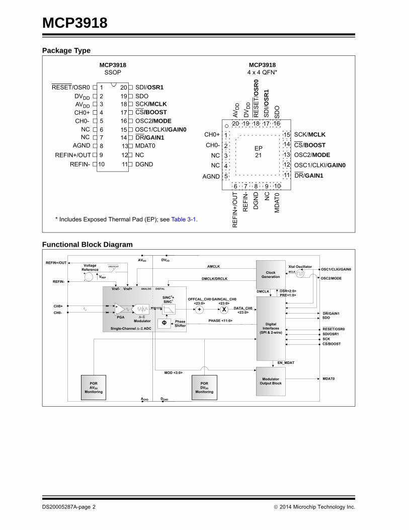
Package Type
Functional Block Diagram
OSC1/CLKI/GAIN0
1
23
4
20
1918
1716
1514
13
5
67
8
OSC2/MODE
SDI/OSR1RESET/OSR0
DVDDAVDD
CH0+CH0-
NC
129
DGND
MDAT0
NC
DR/GAIN1 NCAGND
SDO
1110
REFIN+/OUT
REFIN-
CS/BOOSTSCK/MCLK
SD
O
2
NC
NC
CH0+ SCK/MCLK
CS/BOOST
RE
FIN
+/O
UT
OSC2/MODE
RE
FIN
-
DG
ND
NC
OSC1/CLKI/GAIN0
AV
DD
DV
DD
RE
SE
T/O
SR
0
SD
I/OS
R1
CH0- EP
20
1
19 18 17
3
4
14
13
12
11
6 7 8 9
21
5
10
15
16
AGND
MD
AT
0
DR/GAIN1
MCP39184 x 4 QFN*
MCP3918SSOP
* Includes Exposed Thermal Pad (EP); see Table 3-1.
CH0+
CH0-
Single-Channel ����ADC
ANALOG DIGITAL
-
+
PGA ����Modulator
AMCLK
DMCLK/DRCLK
DATA_CH0<23:0>
REFIN+/OUT
REFIN-
AVDD
AGND DGND
DVDD
MOD<3:0>
PORAVDD
Monitoring
Vref+Vref-
VREFEXTVoltageReference
VREF+
-
PORDVDD
Monitoring
SDO
SDI/OSR1SCK
Xtal OscillatorMCLK
OSC1/CLKI/GAIN0
OSC2/MODE
DR/GAIN1
RESET/OSR0Digital
Interfaces(SPI & 2-wire)
ClockGeneration
ModulatorOutput Block
MDAT0
DMCLK OSR<2:0>PRE<1:0>
EN_MDAT
CS/BOOST
+
OFFCAL_CH0<23:0>
GAINCAL_CH0<23:0>
X
SINC3+SINC1
PhaseShifterΦ PHASE <11:0>
MOD <3:0>
DS20005287A-page 2 2014 Microchip Technology Inc.

MCP3918
1.0 ELECTRICAL CHARACTERISTICS
Absolute Maximum Ratings †
VDD ..................................................................... -0.3V to 4.0VDigital inputs and outputs w.r.t. AGND................ --0.3V to 4.0VAnalog input w.r.t. AGND..................................... ....-2V to +2VVREF input w.r.t. AGND ............................... -0.6V to VDD +0.6VStorage temperature .....................................-65°C to +150°CAmbient temp. with power applied ................-65°C to +125°CSoldering temperature of leads (10 seconds) ............. +300°CESD on the analog inputs (HBM, MM) ................4.0 kV, 200VESD on all other pins (HBM, MM) .......................4.0 kV, 200V
† Notice: Stresses above those listed under “AbsoluteMaximum Ratings” may cause permanent damage tothe device. This is a stress rating only and functionaloperation of the device at those or any otherconditions, above those indicated in the operationallistings of this specification, is not implied. Exposure tomaximum rating conditions for extended periods mayaffect device reliability.
1.1 Electrical Specifications
TABLE 1-1: ANALOG SPECIFICATIONSElectrical Specifications: Unless otherwise indicated, all parameters apply at AVDD = DVDD = 3V, MCLK = 4 MHz; PRE<1:0> = 00; OSR = 256; GAIN = 1; VREFEXT = 0, CLKEXT = 1, DITHER<1:0> = 11; BOOST<1:0> = 10, VCM = 0V; TA = -40°C to +125°C (Note 1); VIN = 1.2 VPP = -0.5 dBFS @ 50/60 Hz on all channels.
Characteristic Sym. Min. Typ. Max. Units Conditions
ADC Performance
Resolution (No Missing Codes)
24 — — bits OSR = 256 or greater
Sampling Frequency fS(DMCLK) — 1 4 MHz For maximum condition, BOOST<1:0> = 11
Output Data Rate fD(DRCLK) — 4 125 ksps For maximum condition, BOOST<1:0> = 11, OSR = 32
Analog Input Absolute Voltage on CH0+/- pins
CH0+/- -1 — +1 V All analog input channels, measured to AGND
Analog Input Leakage Current
IIN — +/-1 — nA RESET<0> = 1, MCLK running continuously
Differential Input Voltage Range
(CH0+-CH0-) -600/GAIN — +600/GAIN mV VREF = 1.2V, proportional to VREF
Offset Error VOS -1 0.2 1 mV Note 5
Offset Error Drift — 0.5 — µV/°C
Gain Error GE -4 — +4 % Note 5
Gain Error Drift — 1 — ppm/°C
Integral Non-Linearity INL — 5 — ppm
Note 1: All specifications are valid down to -45°C.
2: This specification implies that the ADC output is valid over this entire differential range and that there is no distortion or instability across this input range. Dynamic Performance specified at -0.5 dB below the maximum signal range, VIN = 1.2 VPP = 424 mVRMS, VREF = 1.2V @ 50/60 Hz. See Section 4.0 “Terminology and Formulas” for definition. This parameter is established by characterization and not 100% tested.
3: For these operating currents, the following configuration bit settings apply: SHUTDOWN<0> = 0, RESET<0> = 0, VREFEXT = 0, CLKEXT = 0.
4: For these operating currents, the following configuration bit settings apply: SHUTDOWN<0> = 1, VREFEXT = 1, CLKEXT = 1.
5: Applies to all gains. Offset and gain errors depend on the PGA gain setting. See Section 2.0 “Typical Performance Curves” for typical performance.
6: Outside this range, the ADC accuracy is not specified. An extended input range of +/-2V can be applied continuously to the part, with no damage.
7: For proper operation and for optimizing the ADC accuracy, AMCLK should be limited to the maximum frequency defined in Table 5-2, as a function of the BOOST and PGA setting chosen. MCLK can take larger values as long as the prescaler settings (PRE<1:0>) limit AMCLK = MCLK/PRESCALE within the defined range in Table 5-2.
2014 Microchip Technology Inc. DS20005287A-page 3

MCP3918
Measurement Error ME — 0.1 — % Measured with a 10,000:1 dynamic range (from 600 mVPeak to 6 µVPeak), AVDD = DVDD = 3V, measurement points averaging time: 20 seconds.
Differential Input Impedance
ZIN 232 — — k G = 1, proportional to 1/AMCLK
142 — — k G = 2, proportional to 1/AMCLK
72 — — k G = 4, proportional to 1/AMCLK
38 — — k G = 8, proportional to 1/AMCLK
36 — — k G = 16, proportional to 1/AMCLK
33 — — k G = 32, proportional to 1/AMCLK
Signal-to-Noise and Distortion Ratio (Note 2)
SINAD 92 93.5 — dB
Total Harmonic Distor-tion (Note 2)
THD — -107 -103 dBc Includes the first 35 harmonics
Signal-to-Noise Ratio (Note 2)
SNR 92 94 — dB
Spurious-Free Dynamic Range (Note 2)
SFDR — 112 — dBFS
AC Power SupplyRejection
AC PSRR — -73 — dB AVDD = DVDD = 3V + 0.6VPP50/60 Hz, 100/120 Hz
DC Power SupplyRejection
DC PSRR — -73 — dB AVDD = DVDD = 2.7V to 3.6V
DC Common ModeRejection
DC CMRR — -105 — dB VCM from -1V to +1V
TABLE 1-1: ANALOG SPECIFICATIONS (CONTINUED)
Electrical Specifications: Unless otherwise indicated, all parameters apply at AVDD = DVDD = 3V, MCLK = 4 MHz; PRE<1:0> = 00; OSR = 256; GAIN = 1; VREFEXT = 0, CLKEXT = 1, DITHER<1:0> = 11; BOOST<1:0> = 10, VCM = 0V; TA = -40°C to +125°C (Note 1); VIN = 1.2 VPP = -0.5 dBFS @ 50/60 Hz on all channels.
Characteristic Sym. Min. Typ. Max. Units Conditions
Note 1: All specifications are valid down to -45°C.
2: This specification implies that the ADC output is valid over this entire differential range and that there is no distortion or instability across this input range. Dynamic Performance specified at -0.5 dB below the maximum signal range, VIN = 1.2 VPP = 424 mVRMS, VREF = 1.2V @ 50/60 Hz. See Section 4.0 “Terminology and Formulas” for definition. This parameter is established by characterization and not 100% tested.
3: For these operating currents, the following configuration bit settings apply: SHUTDOWN<0> = 0, RESET<0> = 0, VREFEXT = 0, CLKEXT = 0.
4: For these operating currents, the following configuration bit settings apply: SHUTDOWN<0> = 1, VREFEXT = 1, CLKEXT = 1.
5: Applies to all gains. Offset and gain errors depend on the PGA gain setting. See Section 2.0 “Typical Performance Curves” for typical performance.
6: Outside this range, the ADC accuracy is not specified. An extended input range of +/-2V can be applied continuously to the part, with no damage.
7: For proper operation and for optimizing the ADC accuracy, AMCLK should be limited to the maximum frequency defined in Table 5-2, as a function of the BOOST and PGA setting chosen. MCLK can take larger values as long as the prescaler settings (PRE<1:0>) limit AMCLK = MCLK/PRESCALE within the defined range in Table 5-2.
DS20005287A-page 4 2014 Microchip Technology Inc.

MCP3918
Internal Voltage Reference
Tolerance VREF 1.176 1.2 1.224 V VREFEXT = 0, TA = +25°C only
Temperature Coefficient TCVREF — 9 — ppm/°C TA = -40°C to +125°C, VREFEXT = 0
Output Impedance ZOUTVREF — 0.6 — k VREFEXT = 0Internal Voltage Refer-ence Operating Current
AIDDVREF — 54 — µA VREFEXT = 0, SHUTDOWN<0> = 1
Voltage Reference Input
Input Capacitance — — 10 pF
Differential Input Voltage Range (VREF+ – VREF-)
VREF 1.1 — 1.3 V VREFEXT = 1
Absolute Voltageon REFIN+ pin
VREF+ VREF- + 1.1 — VREF- + 1.3 V VREFEXT = 1
Absolute Voltageon REFIN- pin
VREF- -0.1 — +0.1 V REFIN- should be connected to AGND when VREFEXT = 0
Master Clock Input
Master Clock InputFrequency Range
fMCLK — 20 MHz CLKEXT = 1 (Note 7)
Crystal OscillatorOperating FrequencyRange
fXTAL 1 — 20 MHz CLKEXT = 0 (Note 7)
Analog Master Clock AMCLK — — 16 MHz Note 7
Crystal OscillatorOperating Current
DIDDXTAL — 80 — µA CLKEXT = 0
Power Supply
Operating Voltage, Analog AVDD 2.7 — 3.6 V
Operating Voltage, Digital DVDD 2.7 — 3.6 V
Operating Current, Analog (Note 3)
IDD,A — 0.8 1 mA BOOST<1:0> = 00— 1 1.2 mA BOOST<1:0> = 01— 1.3 1.7 mA BOOST<1:0> = 10— 2.2 2.9 mA BOOST<1:0> = 11
TABLE 1-1: ANALOG SPECIFICATIONS (CONTINUED)
Electrical Specifications: Unless otherwise indicated, all parameters apply at AVDD = DVDD = 3V, MCLK = 4 MHz; PRE<1:0> = 00; OSR = 256; GAIN = 1; VREFEXT = 0, CLKEXT = 1, DITHER<1:0> = 11; BOOST<1:0> = 10, VCM = 0V; TA = -40°C to +125°C (Note 1); VIN = 1.2 VPP = -0.5 dBFS @ 50/60 Hz on all channels.
Characteristic Sym. Min. Typ. Max. Units Conditions
Note 1: All specifications are valid down to -45°C.
2: This specification implies that the ADC output is valid over this entire differential range and that there is no distortion or instability across this input range. Dynamic Performance specified at -0.5 dB below the maximum signal range, VIN = 1.2 VPP = 424 mVRMS, VREF = 1.2V @ 50/60 Hz. See Section 4.0 “Terminology and Formulas” for definition. This parameter is established by characterization and not 100% tested.
3: For these operating currents, the following configuration bit settings apply: SHUTDOWN<0> = 0, RESET<0> = 0, VREFEXT = 0, CLKEXT = 0.
4: For these operating currents, the following configuration bit settings apply: SHUTDOWN<0> = 1, VREFEXT = 1, CLKEXT = 1.
5: Applies to all gains. Offset and gain errors depend on the PGA gain setting. See Section 2.0 “Typical Performance Curves” for typical performance.
6: Outside this range, the ADC accuracy is not specified. An extended input range of +/-2V can be applied continuously to the part, with no damage.
7: For proper operation and for optimizing the ADC accuracy, AMCLK should be limited to the maximum frequency defined in Table 5-2, as a function of the BOOST and PGA setting chosen. MCLK can take larger values as long as the prescaler settings (PRE<1:0>) limit AMCLK = MCLK/PRESCALE within the defined range in Table 5-2.
2014 Microchip Technology Inc. DS20005287A-page 5

MCP3918
1.2 Serial Interface Characteristics
Operating Current, Digital IDD,D — 0.2 0.3 mA MCLK = 4 MHz, proportional to MCLK
— 0.7 — mA MCLK = 16 MHz, proportional to MCLK
Shutdown Current, Analog IDDS,A — — 1 µA AVDD pin only (Note 4)
Shutdown Current, Digital IDDS,D — — 2 µA DVDD pin only (Note 4)
Pull-Down Currenton OSC2 Pin(External Clock Mode)
IOSC2 — 35 — µA CLKEXT = 1
TABLE 1-2: SERIAL DC CHARACTERISTICS
Electrical Specifications: Unless otherwise indicated, all parameters apply at DVDD = 2.7 to 3.6 V,TA = -40°C to +125°C (Note 1), CLOAD = 30 pF, applies to all digital I/O.
Characteristic Sym. Min. Typ. Max. Units Conditions
High-Level Input Voltage VIH 0.7 DVDD — — V Schmitt-Triggered
Low-Level Input Voltage VIL — — 0.3 DVDD V Schmitt-Triggered
Input Leakage Current ILI — — ±1 µA CS = DVDD, VIN = DGND to DVDD
Output Leakage Current ILO — — ±1 µA CS = DVDD, VOUT = DGND or DVDD
Hysteresisof Schmitt-Triggered Inputs
VHYS — 300 — mV DVDD = 3.3V only (Note 3)
Low-Level Output Voltage VOL — — 0.4V V IOL = +1.7 mA, DVDD = 3.3V
High-Level Output Voltage VOH DVDD - 0.5 — — V IOH = -1.7 mA, DVDD = 3.3V
Internal Capacitance(All Inputs and Outputs)
CINT — — 7 pF TA = +25°C, SCK = 1.0 MHz,DVDD = 3.3V (Note 2)
Note 1: All specifications are valid down to -45°C.
2: This parameter is periodically sampled and not 100% tested.
3: This parameter is established by characterization and not production tested.
TABLE 1-1: ANALOG SPECIFICATIONS (CONTINUED)
Electrical Specifications: Unless otherwise indicated, all parameters apply at AVDD = DVDD = 3V, MCLK = 4 MHz; PRE<1:0> = 00; OSR = 256; GAIN = 1; VREFEXT = 0, CLKEXT = 1, DITHER<1:0> = 11; BOOST<1:0> = 10, VCM = 0V; TA = -40°C to +125°C (Note 1); VIN = 1.2 VPP = -0.5 dBFS @ 50/60 Hz on all channels.
Characteristic Sym. Min. Typ. Max. Units Conditions
Note 1: All specifications are valid down to -45°C.
2: This specification implies that the ADC output is valid over this entire differential range and that there is no distortion or instability across this input range. Dynamic Performance specified at -0.5 dB below the maximum signal range, VIN = 1.2 VPP = 424 mVRMS, VREF = 1.2V @ 50/60 Hz. See Section 4.0 “Terminology and Formulas” for definition. This parameter is established by characterization and not 100% tested.
3: For these operating currents, the following configuration bit settings apply: SHUTDOWN<0> = 0, RESET<0> = 0, VREFEXT = 0, CLKEXT = 0.
4: For these operating currents, the following configuration bit settings apply: SHUTDOWN<0> = 1, VREFEXT = 1, CLKEXT = 1.
5: Applies to all gains. Offset and gain errors depend on the PGA gain setting. See Section 2.0 “Typical Performance Curves” for typical performance.
6: Outside this range, the ADC accuracy is not specified. An extended input range of +/-2V can be applied continuously to the part, with no damage.
7: For proper operation and for optimizing the ADC accuracy, AMCLK should be limited to the maximum frequency defined in Table 5-2, as a function of the BOOST and PGA setting chosen. MCLK can take larger values as long as the prescaler settings (PRE<1:0>) limit AMCLK = MCLK/PRESCALE within the defined range in Table 5-2.
DS20005287A-page 6 2014 Microchip Technology Inc.

MCP3918
TABLE 1-3: SERIAL AC CHARACTERISTICS
Electrical Specifications: Unless otherwise indicated, all parameters apply at DVDD = 2.7 to 3.6 V,TA = -40°C to +125°C (Note 1), GAIN = 1, CLOAD = 30 pF.
Characteristic Sym Min Typ Max Units Conditions
Serial Clock Frequency fSCK — — 20 MHz
CS Setup Time tCSS 25 — — ns
CS Hold Time tCSH 50 — — ns
CS Disable Time tCSD 50 — — ns
Data Setup Time tSU 5 — — ns
Data Hold Time tHD 10 — — ns
Serial Clock High Time tHI 20 — — ns
Serial Clock Low Time tLO 20 — — ns
Serial Clock Delay Time tCLD 50 — — ns
Serial Clock Enable Time tCLE 50 — — ns
Output Valid from SCK Low tDO — — 25 ns
Output Hold Time tHO 0 — — ns
Output Disable Time tDIS — — 25 ns
Reset Pulse Width (RESET) tMCLR 100 — — ns
Data Transfer Time to DR (Data Ready)
tDODR — — 25 ns Note 2
Modulator Mode Entry to Modulator Data Present
tMODSU — — 100 ns
Data Ready Pulse Low Time tDRP — 1/(2 x DMCLK) — µs
2-Wire Mode Enable Time tMODE — — 50 ns
2-Wire ModeWatchdog Timer
tWATCH 3.5 — 35 µs
Note 1: All specifications are valid down to -45°C.
2: This parameter is established by characterization and not production tested.
TABLE 1-4: TEMPERATURE SPECIFICATIONS
Electrical Specifications: Unless otherwise indicated, all parameters apply at AVDD = 2.7 to 3.6V,DVDD = 2.7 to 3.6V.
Parameters Sym. Min. Typ. Max. Units Conditions
Temperature Ranges
Operating Temperature Range TA -40 — +125 °C Note 1, Note 2
Storage Temperature Range TA -65 — +150 °C
Thermal Package Resistances
Thermal Resistance, 20L 4x4 QFN JA — 46.2 — °C/W
Thermal Resistance, 20L SSOP JA — 87.3 — °C/W
Note 1: The internal junction temperature (TJ) must not exceed the absolute maximum specification of +150°C.
2: All specifications are valid down to -45°C.
2014 Microchip Technology Inc. DS20005287A-page 7

MCP3918
FIGURE 1-1: Serial Output Timing Diagram.
FIGURE 1-2: Serial Input Timing Diagram.
FIGURE 1-3: Data Ready Pulse/Sampling Timing Diagram.
tCSH
tDIS
tHI tLO
fSCK
CS
SCK
SDO MSB out LSB out
SDI
Mode 1,1
Mode 0,0
tHOtDO
DON’T CARE
CS
SCK
SDI LSB inMSB in
Mode 1,1
Mode 0,0
tCSS
tSU tHD
tCSD
tCSHtCLD
tCLE
SDOHi-Z
tHI tLO
fSCK
DR
SCK
tDRP
SDO
1/fD
tDODR
DS20005287A-page 8 2014 Microchip Technology Inc.

MCP3918
FIGURE 1-4: Timing Diagrams, continued.
FIGURE 1-5: Entering 2-Wire Interface Mode Timing Diagram.
CS VIH
Waveform for tDIS
Hi-Z
90%
10%
tDISSDO
SCK
SDO
tDO
Timing Waveform for tDO
SDO
OSC2/MODE
SCK/MCLK
Hi-Z
SPIMode
2-WireMode
AVDD, DVDD
tMODE
0
0
0
2014 Microchip Technology Inc. DS20005287A-page 9

MCP3918
NOTES:
DS20005287A-page 10 2014 Microchip Technology Inc.

MCP3918
2.0 TYPICAL PERFORMANCE CURVES
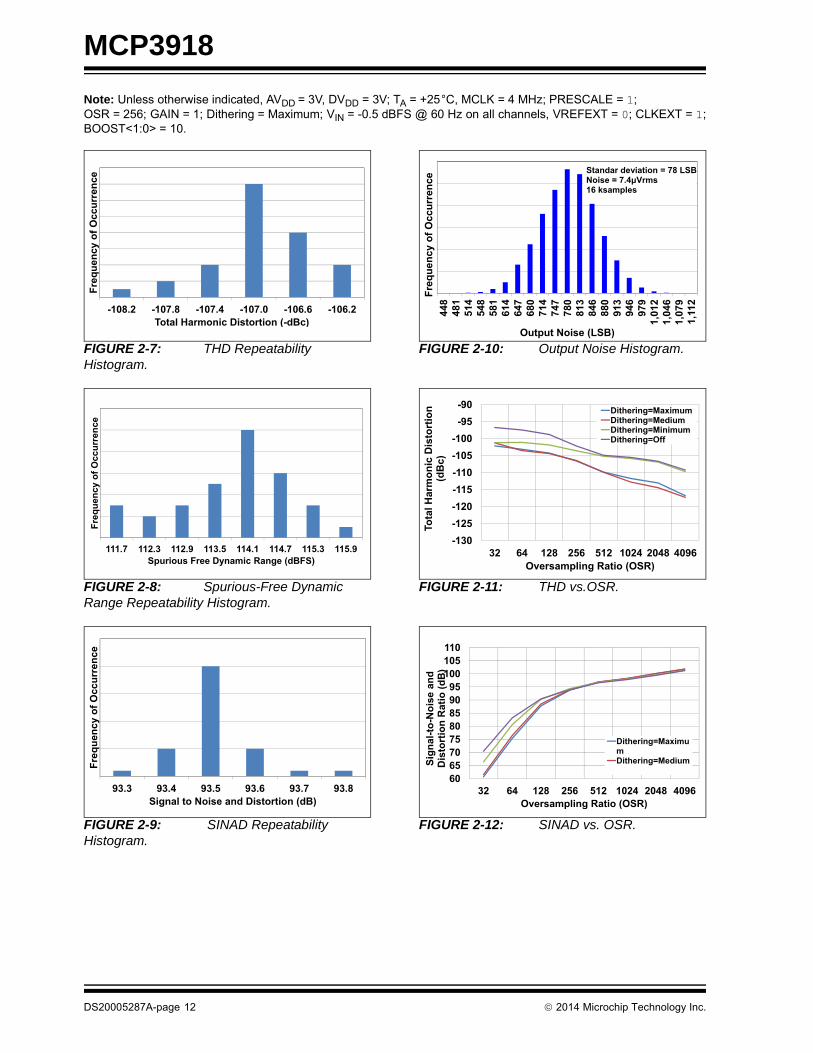
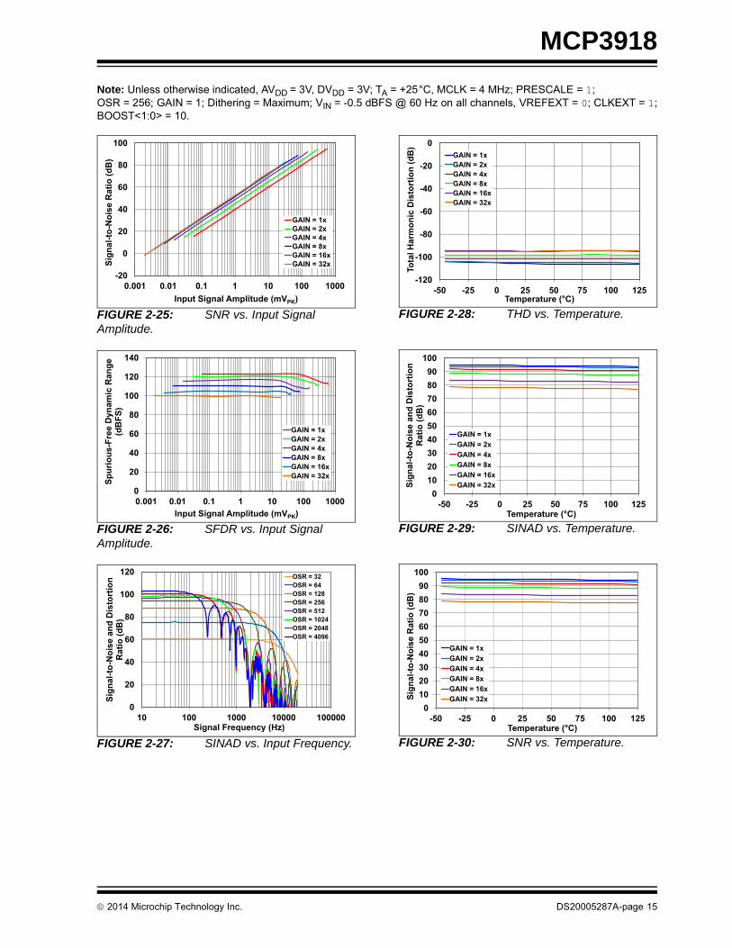
Note: Unless otherwise indicated, AVDD = 3V, DVDD = 3V; TA = +25°C, MCLK = 4 MHz; PRESCALE = 1; OSR = 256; GAIN = 1; Dithering = Maximum; VIN = -0.5 dBFS @ 60 Hz on all channels, VREFEXT = 0; CLKEXT = 1;BOOST<1:0> = 10.
FIGURE 2-1: Spectral Response.
FIGURE 2-2: Spectral Response.
FIGURE 2-3: Spectral Response.
FIGURE 2-4: Spectral Response.
FIGURE 2-5: Measurement Error with 1-Point Calibration.
FIGURE 2-6: Measurement Error with 2-Point Calibration.
Note: The graphs and tables provided following this note are a statistical summary based on a limited number ofsamples and are provided for informational purposes only. The performance characteristics listed hereinare not tested or guaranteed. In some graphs or tables, the data presented may be outside the specifiedoperating range (e.g., outside specified power supply range) and therefore outside the warranted range.
-140-120-100-80-60-40-20
0
Am
plitu
de (d
B)
Vin = -0.5 dBFS @ 60 HzfD = 3.9 kspsOSR = 256Dithering = Off16 ksamples FFT
-180-160140
0 500 1000 1500 2000Frequency (Hz)
200
Vin = -60 dBFS @ 60 Hz
-40-20
B)
fD = 3.9 kspsOSR = 256Dithering = Off
-80-60
de (d
B 16 ksamples FFT
-120-100
mpl
itu
-160-140
A
-180-160
0 500 1000 1500 20000 500 1000 1500 2000Frequency (Hz)
-140-120-100-80-60-40-20
0
Am
plitu
de (d
B)
Vin = -0.5 dBFS @ 60 HzfD = 3.9 kspsOSR = 256Dithering = Maximum16 ksamples FFT
-180-160140
0 500 1000 1500 2000Frequency (Hz)
0
-40-20
0
)
Vin = -60 dBFS @ 60 HzfD = 3.9 kspsOSR = 256
-80-60
de (d
B)
Dithering = Maximum16 ksamples FFT
-120-100
mpl
itud
-160-140A
m
-1800 500 1000 1500 2000
Frequency (Hz)
-1.0%
-0.5%
0.0%
0.5%
1.0%
0.01 0.1 1 10 100 1000
Mea
sure
men
t Err
or (%
)
Current Channel Input Amplitude (mVPeak)
% Error Channel 0,1
-1.0%
-0.5%
0.0%
0.5%
1.0%
0.01 0.1 1 10 100 1000
Mea
sure
men
t Err
or (%
)
Current Channel Input Amplitude (mVPeak)
% Error Channel 0,1
2014 Microchip Technology Inc. DS20005287A-page 11
MCP3918
Note: Unless otherwise indicated, AVDD = 3V, DVDD = 3V; TA = +25°C, MCLK = 4 MHz; PRESCALE = 1; OSR = 256; GAIN = 1; Dithering = Maximum; VIN = -0.5 dBFS @ 60 Hz on all channels, VREFEXT = 0; CLKEXT = 1;BOOST<1:0> = 10.
FIGURE 2-7: THD Repeatability Histogram.
FIGURE 2-8: Spurious-Free Dynamic Range Repeatability Histogram.
FIGURE 2-9: SINAD Repeatability Histogram.
FIGURE 2-10: Output Noise Histogram.
FIGURE 2-11: THD vs.OSR.
FIGURE 2-12: SINAD vs. OSR.
err
ence
f Occ
uen
cy o
fFr
eque
-108.2 -107.8 -107.4 -107.0 -106.6 -106.2
F
Total Harmonic Distortion ( dBc)Total Harmonic Distortion (-dBc)
quen
cy o
f Occ
urre
nce
111.7 112.3 112.9 113.5 114.1 114.7 115.3 115.9
Freq
Spurious Free Dynamic Range (dBFS)
eur
renc
eof
Occ
uen
cyo
Freq
u
93.3 93.4 93.5 93.6 93.7 93.8Signal to Noise and Distortion (dB)Signal to Noise and Distortion (dB)
uenc
y of
Occ
urre
nce Standar deviation = 78 LSB
Noise = 7.4 Vrms16 ksamples
448
481
514
548
581
614
647
680
714
747
780
813
846
880
913
946
979
1,01
21,
046
1,07
91,
112
Freq
u
Output Noise (LSB)
-120-115-110-105-100-95-90
al H
arm
onic
Dis
tort
ion
(dB
c)
Dithering=MaximumDithering=MediumDithering=MinimumDithering=Off
-130-125
32 64 128 256 512 1024 2048 4096
Tot
Oversampling Ratio (OSR)
110
95100105
nd dB)
859095
Noi
se a
Rat
io (d
758085
al-to
-Nor
tion
R
Dithering=Maximu
6570
Sign
Dis
to
Dithering MaximumDithering=Medium
6032 64 128 256 512 1024 2048 4096
Oversampling Ratio (OSR)Oversampling Ratio (OSR)
DS20005287A-page 12 2014 Microchip Technology Inc.
MCP3918
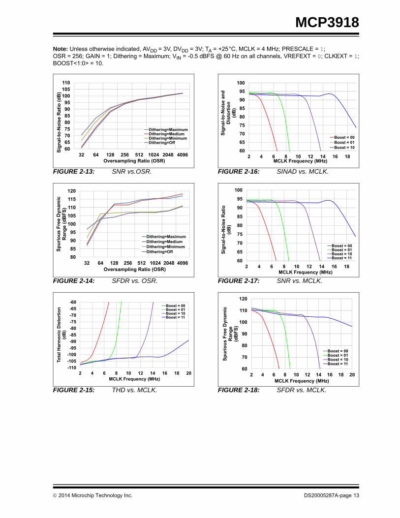
Note: Unless otherwise indicated, AVDD = 3V, DVDD = 3V; TA = +25°C, MCLK = 4 MHz; PRESCALE = 1; OSR = 256; GAIN = 1; Dithering = Maximum; VIN = -0.5 dBFS @ 60 Hz on all channels, VREFEXT = 0; CLKEXT = 1;BOOST<1:0> = 10.
FIGURE 2-13: SNR vs.OSR.
FIGURE 2-14: SFDR vs. OSR.
FIGURE 2-15: THD vs. MCLK.
FIGURE 2-16: SINAD vs. MCLK.
FIGURE 2-17: SNR vs. MCLK.
FIGURE 2-18: SFDR vs. MCLK.
110
95100105
(dB
)
859095
Rat
io(
758085
-Noi
se
Dithering=Maximum
657075
nal-t
o-
Dithering MaximumDithering=MediumDithering=MinimumDithering=Off
6032 64 128 256 512 1024 2048 4096
Sig
O li R ti (OSR)Oversampling Ratio (OSR)
120
110115
nam
ic)
100105110
ee D
yn(d
BFS
)
95100
ous
Fre
Ran
ge(
Dithering=Maximum
8590
Spur
io R gDithering=MediumDithering=MinimumDithering=Off
8032 64 128 256 512 1024 2048 4096
O li R ti (OSR)
Dithering Off
Oversampling Ratio (OSR)
100-95-90-85-80-75-70-65-60
al H
arm
onic
Dis
tort
ion
(dB
)
Boost = 00Boost = 01Boost = 10Boost = 11
-110-105-100
2 4 6 8 10 12 14 16 18 20
Tota
MCLK Frequency (MHz)
100
90
95
e an
d
80
85
o-N
oise
tort
ion
dB)
75
80
gnal
-to Dis
t (
65
70Sig
Boost = 00Boost = 01
602 4 6 8 10 12 14 16 18
Boost = 10
MCLK Frequency (MHz)
100
90
95
tio80
85is
e R
at)
75
80-to
-No
(dB
)
65
70
Sign
al
Boost = 00Boost = 01Boost = 10
602 4 6 8 10 12 14 16 18
Boost = 10Boost = 11
MCLK Frequency (MHz)
120
110
amic
90
100
ee D
ynge FS
)
80
90
ous
Fre
Ran
(dB
F
70
80
Spur
io Boost = 00Boost = 01Boost = 10
602 4 6 8 10 12 14 16 18 20
Boost = 11
2 4 6 8 10 12 14 16 18 20MCLK Frequency (MHz)
2014 Microchip Technology Inc. DS20005287A-page 13
MCP3918
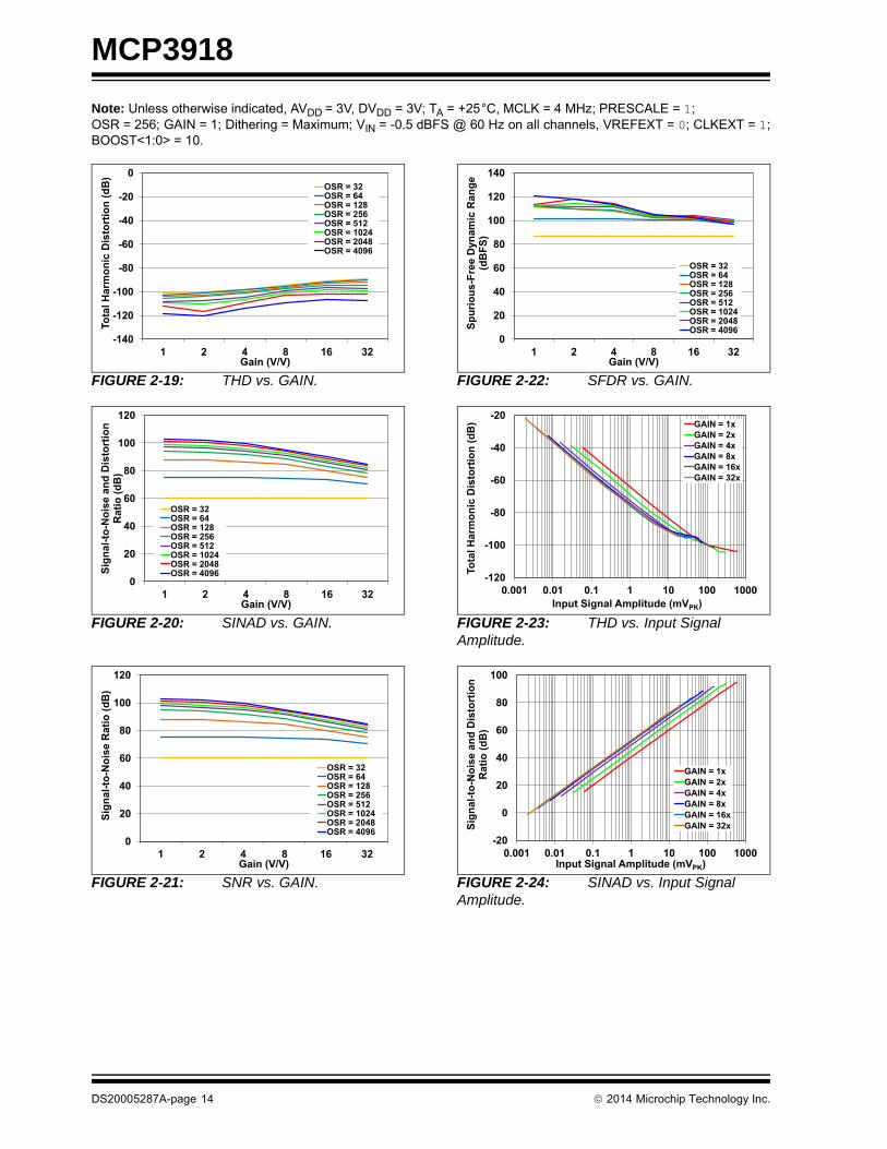
Note: Unless otherwise indicated, AVDD = 3V, DVDD = 3V; TA = +25°C, MCLK = 4 MHz; PRESCALE = 1; OSR = 256; GAIN = 1; Dithering = Maximum; VIN = -0.5 dBFS @ 60 Hz on all channels, VREFEXT = 0; CLKEXT = 1;BOOST<1:0> = 10.
FIGURE 2-19: THD vs. GAIN.
FIGURE 2-20: SINAD vs. GAIN.
FIGURE 2-21: SNR vs. GAIN.
FIGURE 2-22: SFDR vs. GAIN.
FIGURE 2-23: THD vs. Input Signal Amplitude.
FIGURE 2-24: SINAD vs. Input Signal Amplitude.
-140
-120
-100
-80
-60
-40
-20
0
1 2 4 8 16 32
Tota
l Har
mon
ic D
isto
rtio
n (d
B)
Gain (V/V)
OSR = 32OSR = 64OSR = 128OSR = 256OSR = 512OSR = 1024OSR = 2048OSR = 4096
0
20
40
60
80
100
120
1 2 4 8 16 32
Sign
al-to
-Noi
se a
nd D
isto
rtio
n R
atio
(dB
)
Gain (V/V)
OSR = 32OSR = 64OSR = 128OSR = 256OSR = 512OSR = 1024OSR = 2048OSR = 4096
0
20
40
60
80
100
120
1 2 4 8 16 32
Sign
al-to
-Noi
se R
atio
(dB
)
Gain (V/V)
OSR = 32OSR = 64OSR = 128OSR = 256OSR = 512OSR = 1024OSR = 2048OSR = 4096
0
20
40
60
80
100
120
140
1 2 4 8 16 32
Spur
ious
-Fre
e D
ynam
ic R
ange
(d
BFS
)
Gain (V/V)
OSR = 32OSR = 64OSR = 128OSR = 256OSR = 512OSR = 1024OSR = 2048OSR = 4096
-120
-100
-80
-60
-40
-20
0.001 0.01 0.1 1 10 100 1000
Tota
l Har
mon
ic D
isto
rtio
n (d
B)
Input Signal Amplitude (mVPK)
GAIN = 1xGAIN = 2xGAIN = 4xGAIN = 8xGAIN = 16xGAIN = 32x
-20
0
20
40
60
80
100
0.001 0.01 0.1 1 10 100 1000
Sign
al-to
-Noi
se a
nd D
isto
rtio
n R
atio
(dB
)
Input Signal Amplitude (mVPK)
GAIN = 1xGAIN = 2xGAIN = 4xGAIN = 8xGAIN = 16xGAIN = 32x
DS20005287A-page 14 2014 Microchip Technology Inc.
MCP3918
Note: Unless otherwise indicated, AVDD = 3V, DVDD = 3V; TA = +25°C, MCLK = 4 MHz; PRESCALE = 1; OSR = 256; GAIN = 1; Dithering = Maximum; VIN = -0.5 dBFS @ 60 Hz on all channels, VREFEXT = 0; CLKEXT = 1;BOOST<1:0> = 10.
FIGURE 2-25: SNR vs. Input Signal Amplitude.
FIGURE 2-26: SFDR vs. Input Signal Amplitude.
FIGURE 2-27: SINAD vs. Input Frequency.
FIGURE 2-28: THD vs. Temperature.
FIGURE 2-29: SINAD vs. Temperature.
FIGURE 2-30: SNR vs. Temperature.
-20
0
20
40
60
80
100
0.001 0.01 0.1 1 10 100 1000
Sign
al-to
-Noi
se R
atio
(dB
)
Input Signal Amplitude (mVPK)
GAIN = 1xGAIN = 2xGAIN = 4xGAIN = 8xGAIN = 16xGAIN = 32x
0
20
40
60
80
100
120
140
0.001 0.01 0.1 1 10 100 1000
Spur
ious
-Fre
e D
ynam
ic R
ange
(d
BFS
)
Input Signal Amplitude (mVPK)
GAIN = 1xGAIN = 2xGAIN = 4xGAIN = 8xGAIN = 16xGAIN = 32x
0
20
40
60
80
100
120
10 100 1000 10000 100000
Sign
al-to
-Noi
se a
nd D
isto
rtio
n R
atio
(dB
)
Signal Frequency (Hz)
OSR = 32OSR = 64OSR = 128OSR = 256OSR = 512OSR = 1024OSR = 2048OSR = 4096
-120
-100
-80
-60
-40
-20
0
-50 -25 0 25 50 75 100 125
Tota
l Har
mon
ic D
isto
rtio
n(d
B)
Temperature (°C)
GAIN = 1xGAIN = 2xGAIN = 4xGAIN = 8xGAIN = 16xGAIN = 32x
0102030405060708090
100
-50 -25 0 25 50 75 100 125
Sign
al-to
-Noi
se a
nd D
isto
rtio
n R
atio
(dB
)
Temperature (°C)
GAIN = 1xGAIN = 2xGAIN = 4xGAIN = 8xGAIN = 16xGAIN = 32x
0102030405060708090
100
-50 -25 0 25 50 75 100 125
Sign
al-to
-Noi
se R
atio
(dB
)
Temperature (°C)
GAIN = 1xGAIN = 2xGAIN = 4xGAIN = 8xGAIN = 16xGAIN = 32x
2014 Microchip Technology Inc. DS20005287A-page 15
MCP3918
Note: Unless otherwise indicated, AVDD = 3V, DVDD = 3V; TA = +25°C, MCLK = 4 MHz; PRESCALE = 1; OSR = 256; GAIN = 1; Dithering = Maximum; VIN = -0.5 dBFS @ 60 Hz on all channels, VREFEXT = 0; CLKEXT = 1;BOOST<1:0> = 10.
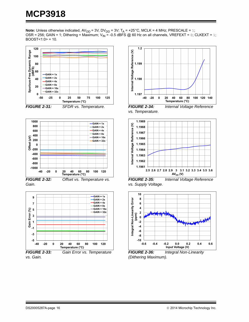
FIGURE 2-31: SFDR vs. Temperature.
FIGURE 2-32: Offset vs. Temperature vs. Gain.
FIGURE 2-33: Gain Error vs. Temperature vs. Gain.
FIGURE 2-34: Internal Voltage Reference vs. Temperature.
FIGURE 2-35: Internal Voltage Reference vs. Supply Voltage.
FIGURE 2-36: Integral Non-Linearity (Dithering Maximum).
0
20
40
60
80
100
120
-50 -25 0 25 50 75 100 125
Spur
ious
-Fre
e D
ynam
ic R
ange
(d
BFS
)
Temperature (°C)
GAIN = 1xGAIN = 2xGAIN = 4xGAIN = 8xGAIN = 16xGAIN = 32x
-1000-800-600-400-200
0200400600800
1000
-40 -20 0 20 40 60 80 100 120
Offs
et (µ
V)
Temperature (°C)
GAIN = 1xGAIN = 2xGAIN = 4xGAIN = 8xGAIN = 16xGAIN = 32x
-5
-3
-1
1
3
5
7
9
-40 -20 0 20 40 60 80 100 120
Gai
n Er
ror (
%)
Temperature (°C)
GAIN = 1xGAIN = 2xGAIN = 4xGAIN = 8xGAIN = 16xGAIN = 32x
1.197
1.198
1.199
1.2
-40 -20 0 20 40 60 80 100 120 140
Inte
rnal
Vol
tage
Ref
eren
ce (V
)
Temperature (°C)
1.1961
1.1962
1.1963
1.1964
1.1965
1.1966
1.1967
1.1968
1.1969
2.5 2.6 2.7 2.8 2.9 3 3.1 3.2 3.3 3.4 3.5 3.6
Inte
rnal
Vol
tage
Ref
eren
ce (V
)
AVDD (V)
-10-8-6-4-202468
10
-0.6 -0.4 -0.2 0.0 0.2 0.4 0.6
Inte
gral
Non
-Lin
earit
y Er
ror
(ppm
)
Input Voltage (V)
DS20005287A-page 16 2014 Microchip Technology Inc.
MCP3918
Note: Unless otherwise indicated, AVDD = 3V, DVDD = 3V; TA = +25°C, MCLK = 4 MHz; PRESCALE = 1; OSR = 256; GAIN = 1; Dithering = Maximum; VIN = -0.5 dBFS @ 60 Hz on all channels, VREFEXT = 0; CLKEXT = 1;BOOST<1:0> = 10.
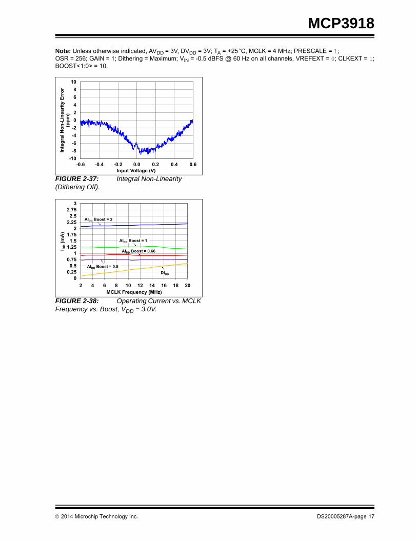
FIGURE 2-37: Integral Non-Linearity (Dithering Off).
FIGURE 2-38: Operating Current vs. MCLK Frequency vs. Boost, VDD = 3.0V.
-10-8-6-4-202468
10
-0.6 -0.4 -0.2 0.0 0.2 0.4 0.6
Inte
gral
Non
-Lin
earit
y Er
ror
(ppm
)
Input Voltage (V)
00.25
0.50.75
11.25
1.51.75
22.25
2.52.75
3
2 4 6 8 10 12 14 16 18 20
I DD
(mA
)
MCLK Frequency (MHz)
AIDD Boost = 0.5
AIDD Boost = 0.66
AIDD Boost = 1
DIDD
AIDD Boost = 2
2014 Microchip Technology Inc. DS20005287A-page 17

MCP3918
NOTES:
DS20005287A-page 18 2014 Microchip Technology Inc.

MCP3918
3.0 PIN DESCRIPTION
The descriptions of the pins are listed in Table 3-1.
3.1 Master Reset/OSR0 Logic Input (RESET/OSR0)
In SPI mode, this pin is active low and places the entirechip in a Reset state when active.
When RESET is logic low, all registers are reset to theirdefault value, no communication can take place, andno clock is distributed inside the part, except in theinput structure if MCLK is applied (if MCLK is idle, thenno clock is distributed). This state is equivalent to aPower-On Reset (POR) state.
Since the default state of the ADC is on, the analogpower consumption when RESET is logic low isequivalent to when RESET is logic high. Only the digitalpower consumption is largely reduced because thiscurrent consumption is essentially dynamic and isreduced drastically when there is no clock running.
If MCLK is applied when RESET is logic low, all theanalog biases are enabled during a reset, so that thepart is fully operational just after a RESET rising edge.If MCLK is not applied, there is a time after a hard resetwhen the conversion may not accurately correspond tothe start-up of the input structure.
This input is Schmitt-triggered.
In 2-Wire Interface mode, this is the OSR0 logic selectpin (see Section 7.0 “2-Wire Serial InterfaceDescription” for the logic input table for OSR0 andOSR1). The pin state is latched when the MODEchanges to 2-Wire Interface mode, and is relatched ateach watchdog timer reset.
TABLE 3-1: SIX-CHANNEL MCP3918 PIN FUNCTION TABLE
MCP3918SSOP
MCP3918QFN
Symbol Function
1 18 RESET/OSR0 Master Reset Logic Input Pin or OSR0 Logic Input Pin
2 19 DVDD Digital Power Supply Pin
3 20 AVDD Analog Power Supply Pin
4 1 CH0+ Non-Inverting Analog Input Pin for Channel 0
5 2 CH0- Inverting Analog Input Pin for Channel 0
6 3 NC Not connected
7 4 NC Not connected
8 5 AGND Analog Ground Pin, Return Path for internal analog circuitry
9 6 REFIN+/OUT Non-Inverting Voltage Reference Input and Internal Reference Output Pin
10 7 REFIN- Inverting Voltage Reference Input Pin
11 8 DGND Digital Ground Pin, Return Path for internal digital circuitry
12 9 NC Not connected
13 10 MDAT0 Modulator Data Output Pin for Channel 0
14 11 DR/GAIN1 Data Ready Signal Output Pin or GAIN1 Logic Input Pin
15 12 OSC1/CLKI/GAIN0 Oscillator Crystal Connection Pin or External Clock Input Pin or GAIN0 Logic Input Pin
16 13 OSC2/MODE Oscillator Crystal Connection Input Pin or Serial Interface Mode Logic Input Pin
17 14 CS/BOOST Serial Interface Chip Select Input Pin or BOOST Logic Input Pin
18 15 SCK/MCLK Serial Interface Clock Pin or Master Clock Input Pin
19 16 SDO Serial Interface Data Input Pin
20 17 SDI/OSR1 Serial Interface Data Input Pin or OSR1 Logic Input Pin
— 21 EP Exposed Thermal Pad
2014 Microchip Technology Inc. DS20005287A-page 19
MCP3918
3.2 Digital VDD (DVDD)
DVDD is the power supply voltage for the digital circuitrywithin the MCP3918. For optimal performance, it isrecommended to connect appropriate bypasscapacitors (typically a 10 µF in parallel with a 0.1 µFceramic). DVDD should be maintained between 2.7Vand 3.6V for specified operation.
3.3 Analog Power Supply (AVDD)
AVDD is the power supply voltage for the analogcircuitry within the MCP3918. It is recommended toconnect appropriate bypass capacitors (typically a10 µF in parallel with a 0.1 µF ceramic). AVDD shouldbe maintained between 2.7V and 3.6V for specifiedoperation.
3.4 ADC Differential Analog Inputs (CH0+/CH0-)
The CH0+/- pins are the fully differential analog voltageinputs for the delta-sigma ADC.
The linear and specified region of the channels isdependent on the PGA gain. This region correspondsto a differential voltage range of ±600 mV/GAIN withVREF = 1.2V.
The maximum absolute voltage, with respect to AGND,for each CH0+/- input pin is ±1V with no distortion and±2V with no breaking after continuous voltage. Thismaximum absolute voltage is not proportional to theVREF voltage.
3.5 Analog Ground (AGND)
AGND is the ground reference voltage for the analogcircuitry within the MCP3918. For optimal performance,it is recommended to connect it to the same groundnode voltage as DGND, preferably with a starconnection.
If an analog ground plane is available, it isrecommended that these pins be tied to this plane ofthe Printed Circuit Board (PCB). This plane should alsoreference all other analog circuitry in the system.
3.6 Non-Inverting Reference Input, Internal Reference Output (REFIN+/OUT)
This pin is the non-inverting side of the differentialvoltage reference input for the ADC or the internalvoltage reference output.
When VREFEXT = 1, an external voltage referencesource can be used, and the internal voltage referenceis disabled. When using an external differential voltagereference, it should be connected to its VREF+ pin.When using an external single-ended reference, itshould be connected to this pin.
When VREFEXT = 0, the internal voltage reference isenabled and connected to this pin through a switch.This voltage reference has minimal drive capability andthus needs proper buffering and bypass capacitances(a 0.1 µF ceramic capacitor is sufficient in most cases),if used as a voltage source.
If the voltage reference is only used as an internalVREF, adding bypass capacitance on REFIN+/OUT isnot necessary for keeping ADC accuracy, but a minimal0.1 µF ceramic capacitance can be connected to avoidEMI/EMC susceptibility issues due to the antennacreated by the REFIN+/OUT pin if left floating.
3.7 Inverting Reference Input (REFIN-)
This pin is the inverting side of the differential voltagereference input for the ADC. When using an externaldifferential voltage reference, it should be connected toits VREF- pin. When using an external single-endedvoltage reference, or when VREFEXT = 0 (default) andusing the internal voltage reference, the pin should bedirectly connected to AGND.
3.8 Digital Ground Connection (DGND)
DGND is the ground reference voltage for the digitalcircuitry within the MCP3918. For optimal performance,it is recommended to connect it to the same groundnode voltage as AGND, preferably with a starconnection.
If a digital ground plane is available, it is recommendedthat this pin be tied to this plane of the PCB. This planeshould also reference all other digital circuitry in thesystem.
DS20005287A-page 20 2014 Microchip Technology Inc.
MCP3918
2014 Microchip Technology Inc. DS20005287A-page 21
3.9 Modulator Output(MDAT0)
MDAT0 is the output pin for the modulator serial bitstreams of the ADC. This pin is high-impedance whenthe EN_MDAT bit is logic low. When the EN_MDAT bitis enabled, the modulator bit stream of the ADC ispresent on the pin and updated at the AMCLKfrequency (see Section 5.3.5 “Modulator OutputBlock” for a complete description of the modulatoroutput). This pin can be directly connected to an MCUor a DSP when a specific digital filtering is needed.When the MDAT0 output pin is enabled, the DR outputis disabled. In 2-Wire Interface mode, this pin isautomatically inactive. Its state is high-impedanceduring the 2-Wire mode (therefore this pin can be leftgrounded in applications using exclusively the 2-WireInterface mode; this configuration improves theEMI/EMC susceptibility of the device).
3.10 Data Ready Output/GAIN1 Logic Input (DR/GAIN1)
In SPI mode, the Data Ready pin indicates if a newconversion result is ready to be read. The default stateof this pin is logic high when DR_HIZ = 1 and ishigh-impedance when DR_HIZ = 0 (default). Aftereach conversion is finished, a logic low pulse will takeplace on the Data Ready pin to indicate the conversionresult is ready as an interrupt. This pulse issynchronous with the master clock and has a definedand constant width.
The Data Ready pin is independent from the SPIinterface and acts like an interrupt output. The DataReady pin state is not latched, and the pulse width (andperiod) are both determined by the MCLK frequency,oversampling rate, and internal clock prescale settings.The Data Ready pulse width is equal to half a DMCLKperiod and the frequency of the pulses is equal toDRCLK (see Figure 1-3).
In 2-Wire Interface mode, this is the GAIN1 logic selectpin. See Section 7.0 “2-Wire Serial InterfaceDescription” for the logic input table for GAIN0 andGAIN1. The pin state is latched when the MODEchanges to 2-Wire Interface mode, and is relatched ateach watchdog timer reset.
3.11 Crystal Oscillator/Master Clock Input/GAIN0 Logic Input(OSC1/CLKI/GAIN0)
In SPI mode, OSC1/CLKI and OSC2 provide themaster clock for the device. When CLKEXT = 0, aresonant crystal or clock source with a similarsinusoidal waveform must be placed across the OSC1and OSC2 pins to ensure proper operation.
The typical clock frequency specified is 4 MHz. Forproper operation and in order to optimize ADCaccuracy, AMCLK should be limited to the maximumfrequency defined in Table 5-2 for the function of theBOOST and PGA setting chosen. MCLK can takelarger values as long as the prescaler settings(PRE<1:0>) limit AMCLK = MCLK/PRESCALE in thedefined range in Table 5-2. Appropriate loadcapacitance should be connected to these pins forproper operation.
In 2-Wire Interface mode, this is the GAIN0 logic selectpin. See Section 7.0 “2-Wire Serial InterfaceDescription” for the logic input table for GAIN0 andGAIN1. The pin state is latched when the MODEchanges to 2-Wire Interface mode, and is relatched ateach watchdog timer reset.
3.12 Crystal Oscillator Output/ Interface MODE Logic Input (OSC2/MODE)
When CLKEXT = 0 (default), a resonant crystal orclock source with a similar sinusoidal waveform mustbe placed across the OSC1 and OSC2 pins to ensureproper operation. Appropriate load capacitance shouldbe connected to these pins for proper operation.
When CLKEXT = 1 (default condition at POR), this pinis the MODE selection pin for the digital interface.When MODE is logic low, the SPI interface is selected(see Section 6.0 “SPI Serial Interface Description”).When MODE is logic high, the 2-Wire interface isselected (see Section 7.0 “2-Wire Serial InterfaceDescription”). The MODE input is latched after aPOR, a Master Reset and/or a Watchdog Timer Reset.
Note: This pin should not be left floating whenthe DR_HIZ bit is low; a 100 k pull-upresistor connected to DVDD isrecommended.
Note: When CLKEXT = 1, the crystal oscillatoris disabled. OSC1 becomes the masterclock input CLKI, a direct path for anexternal clock source. One examplewould be a clock source generated by anMCU.
MCP3918
3.13 Chip Select/ Boost Logic Input (CS/BOOST)
In SPI mode, this pin is the SPI chip select that enablesserial communication. When this pin is logic high, nocommunication can take place. A chip select fallingedge initiates serial communication, and a chip selectrising edge terminates the communication. Nocommunication can take place even when CS is logiclow, if RESET is also logic low.
This input is Schmitt-triggered.
In the 2-Wire Interface mode, this is the Boost logicselect pin. See Section 7.0 “2-Wire Serial InterfaceDescription” for the logic input table for Boost. The pinstate is latched when the mode changes to 2-WireInterface mode, and is re-latched at each watchdogtimer reset.
3.14 Serial Data Clock/Master Clock Input (SCK/MCLK)
In SPI mode, this is the serial clock pin for SPIcommunication. Data is clocked into the device on therising edge of SCK. Data is clocked out of the device onthe falling edge of SCK.
The MCP3918 SPI interface is compatible with SPI 0,0and 1,1 modes. SPI modes can be changed during aCS high time.
The maximum clock speed specified is 20 MHz. SCKand MCLK are two different and asynchronous clocks;SCK is only required when a communication happens,while MCLK is continuously required when the part isconverting analog inputs.
This input is Schmitt-triggered.
In the 2-Wire Interface mode, this pin is defining themaster clock of the device (MCLK) and the serial clock(SCK) for the interface simultaneously. In this mode,the clock has to be provided continuously to ensureproper operation. See Section 7.0 “2-Wire SerialInterface Description” for more information andtiming diagrams of the 2-Wire interface protocol.
3.15 Serial Data Output (SDO)
This is the SPI data output pin. Data is clocked out ofthe device on the falling edge of SCK.
This pin remains in a high-impedance state during thecommand byte. It also stays high-impedance during theentire communication for Write commands and whenthe CS pin is logic high or when the RESET pin is logiclow. This pin is active only when a Read command isprocessed. The interface is half-duplex (inputs andoutputs do not happen at the same time).
In the 2-Wire Interface Mode, this pin is the only digitaloutput pin, and sends synchronous frames at eachdata ready with data bits clocked out on the falling edgeof SCK.
3.16 Serial Data/OSR1 Logic Input (SDI/OSR1)
In SPI mode, this is the SPI data input pin. Data isclocked into the device on the rising edge of SCK.When CS is logic low, this pin is used to communicatewith 8-bit commands followed by data bytes that can be16-/24- or 32-bit wide. The interface is half-duplex(inputs and outputs do not happen at the same time).
Each communication starts with a chip select fallingedge followed by an 8-bit command word, enteredthrough the SDI pin. Each command is either a Read ora Write command. Toggling SDI during a Readcommand has no effect.
This input is Schmitt-triggered.
In 2-Wire Interface mode, this is the OSR1 logic selectpin. See Section 7.0 “2-Wire Serial InterfaceDescription” for the logic input table for OSR0 andOSR1. The pin state is latched when the modechanges to 2-Wire Interface Mode, and is relatched ateach watchdog timer reset.
3.17 Exposed Pad (EP)
Exposed Thermal Pad. This pin must be connected toAGND for optimal accuracy and thermal performance.This pad can also be left floating if necessary.Connecting it to AGND is preferable for the lowest noiseperformance and best thermal behavior.
DS20005287A-page 22 2014 Microchip Technology Inc.

MCP3918
4.0 TERMINOLOGY AND FORMULAS
This section defines the terms and formulas usedthroughout this data sheet. The following terms aredefined:
• MCLK – Master Clock
• AMCLK – Analog Master Clock
• DMCLK – Digital Master Clock
• DRCLK – Data Rate Clock
• OSR – Oversampling Ratio
• Offset Error
• Gain Error
• Integral Non-Linearity Error
• Signal-to-Noise Ratio (SNR)
• Signal-to-Noise and Distortion Ratio (SINAD)
• Total Harmonic Distortion (THD)
• Spurious-Free Dynamic Range (SFDR)
• MCP3918 Delta-Sigma Architecture
• Idle Tones
• Dithering
• PSRR
• CMRR
• ADC Reset Mode
• Hard Reset Mode (RESET = 0)
• ADC Shutdown Mode
• Full Shutdown Mode
4.1 MCLK – Master Clock
This is the fastest clock present on the device. This isthe frequency of the crystal placed at the OSC1/OSC2inputs when CLKEXT = 0 or the frequency of the clockinput at the OSC1/CLKI when CLKEXT = 1. In the 2-Wire mode, this is the frequency present at the SCKinput pin. See Figure 4-1.
4.2 AMCLK – Analog Master Clock
AMCLK is the clock frequency that is present on theanalog portion of the device, after prescaling hasoccurred via the PRE<1:0> bits in the CONFIG0register (see Equation 4-1). The analog portionincludes the PGA and one delta-sigma modulator.
EQUATION 4-1:
FIGURE 4-1: Clock Sub-Circuitry.
4.3 DMCLK – Digital Master Clock
This is the clock frequency that is present on the digitalportion of the device, after prescaling and division byfour (Equation 4-2). This is also the samplingfrequency, which is the rate at which the modulatoroutputs are refreshed. Each period of this clockcorresponds to one sample and one modulator output.See Figure 4-1.
EQUATION 4-2:
4.4 DRCLK – Data Rate Clock
This is the output data rate, i.e. the rate at which theADC outputs new data. Each new data is signaled by aData Ready pulse on the Data Ready pin.
This data rate is dependent on the OSR and theprescaler with the formula in Equation 4-3.
EQUATION 4-3:
TABLE 4-1: MCP3918 OVERSAMPLING RATIO SETTINGS
CONFIG0 Analog Master Clock Prescale PRE<1:0>
0 0 AMCLK = MCLK/1 (default)
0 1 AMCLK = MCLK/2
1 0 AMCLK = MCLK/4
1 1 AMCLK = MCLK/8
AMCLKMCLK
PRESCALE-------------------------------=
Xtal Oscillator
MCLK
OSC1
OSC2Multiplexer
OUT
0
1
1/PRESCALE 1/4 1/OSRAMCLK DMCLK DRCLK
Clock Divider Clock Divider Clock Divider
OSR<2:0>PRE<1:0>CLKEXT
Multiplexer
OUT
0
1
MODE
SCK
DMCLKAMCLK
4---------------------
MCLK4 PRESCALE----------------------------------------= =
DRCLKDMCLK
OSR----------------------
AMCLK4 OSR---------------------
MCLK4 OSR PRESCALE-----------------------------------------------------------= = =
2014 Microchip Technology Inc. DS20005287A-page 23
MCP3918
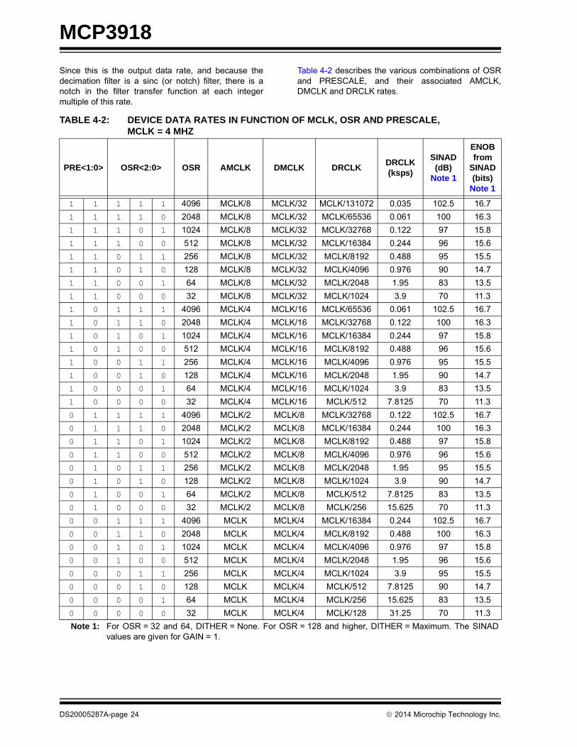
Since this is the output data rate, and because thedecimation filter is a sinc (or notch) filter, there is anotch in the filter transfer function at each integermultiple of this rate.
Table 4-2 describes the various combinations of OSRand PRESCALE, and their associated AMCLK,DMCLK and DRCLK rates.
TABLE 4-2: DEVICE DATA RATES IN FUNCTION OF MCLK, OSR AND PRESCALE, MCLK = 4 MHZ
PRE<1:0> OSR<2:0> OSR AMCLK DMCLK DRCLKDRCLK(ksps)
SINAD(dB)
Note 1
ENOB from
SINAD(bits)
Note 1
1 1 1 1 1 4096 MCLK/8 MCLK/32 MCLK/131072 0.035 102.5 16.7
1 1 1 1 0 2048 MCLK/8 MCLK/32 MCLK/65536 0.061 100 16.3
1 1 1 0 1 1024 MCLK/8 MCLK/32 MCLK/32768 0.122 97 15.8
1 1 1 0 0 512 MCLK/8 MCLK/32 MCLK/16384 0.244 96 15.6
1 1 0 1 1 256 MCLK/8 MCLK/32 MCLK/8192 0.488 95 15.5
1 1 0 1 0 128 MCLK/8 MCLK/32 MCLK/4096 0.976 90 14.7
1 1 0 0 1 64 MCLK/8 MCLK/32 MCLK/2048 1.95 83 13.5
1 1 0 0 0 32 MCLK/8 MCLK/32 MCLK/1024 3.9 70 11.3
1 0 1 1 1 4096 MCLK/4 MCLK/16 MCLK/65536 0.061 102.5 16.7
1 0 1 1 0 2048 MCLK/4 MCLK/16 MCLK/32768 0.122 100 16.3
1 0 1 0 1 1024 MCLK/4 MCLK/16 MCLK/16384 0.244 97 15.8
1 0 1 0 0 512 MCLK/4 MCLK/16 MCLK/8192 0.488 96 15.6
1 0 0 1 1 256 MCLK/4 MCLK/16 MCLK/4096 0.976 95 15.5
1 0 0 1 0 128 MCLK/4 MCLK/16 MCLK/2048 1.95 90 14.7
1 0 0 0 1 64 MCLK/4 MCLK/16 MCLK/1024 3.9 83 13.5
1 0 0 0 0 32 MCLK/4 MCLK/16 MCLK/512 7.8125 70 11.3
0 1 1 1 1 4096 MCLK/2 MCLK/8 MCLK/32768 0.122 102.5 16.7
0 1 1 1 0 2048 MCLK/2 MCLK/8 MCLK/16384 0.244 100 16.3
0 1 1 0 1 1024 MCLK/2 MCLK/8 MCLK/8192 0.488 97 15.8
0 1 1 0 0 512 MCLK/2 MCLK/8 MCLK/4096 0.976 96 15.6
0 1 0 1 1 256 MCLK/2 MCLK/8 MCLK/2048 1.95 95 15.5
0 1 0 1 0 128 MCLK/2 MCLK/8 MCLK/1024 3.9 90 14.7
0 1 0 0 1 64 MCLK/2 MCLK/8 MCLK/512 7.8125 83 13.5
0 1 0 0 0 32 MCLK/2 MCLK/8 MCLK/256 15.625 70 11.3
0 0 1 1 1 4096 MCLK MCLK/4 MCLK/16384 0.244 102.5 16.7
0 0 1 1 0 2048 MCLK MCLK/4 MCLK/8192 0.488 100 16.3
0 0 1 0 1 1024 MCLK MCLK/4 MCLK/4096 0.976 97 15.8
0 0 1 0 0 512 MCLK MCLK/4 MCLK/2048 1.95 96 15.6
0 0 0 1 1 256 MCLK MCLK/4 MCLK/1024 3.9 95 15.5
0 0 0 1 0 128 MCLK MCLK/4 MCLK/512 7.8125 90 14.7
0 0 0 0 1 64 MCLK MCLK/4 MCLK/256 15.625 83 13.5
0 0 0 0 0 32 MCLK MCLK/4 MCLK/128 31.25 70 11.3
Note 1: For OSR = 32 and 64, DITHER = None. For OSR = 128 and higher, DITHER = Maximum. The SINADvalues are given for GAIN = 1.
DS20005287A-page 24 2014 Microchip Technology Inc.
MCP3918
4.5 OSR – Oversampling Ratio
This is the ratio of the sampling frequency to the outputdata rate: OSR = DMCLK/DRCLK. The default OSR is256, with MCLK = 4 MHz, PRESCALE = 1,AMCLK = 4 MHz, fS = 1 MHz, and fD = 3.90625 ksps.The bits in Table 4-3, available in the CONFIG0register, are used to change the oversampling ratio(OSR).
4.6 Offset Error
This is the error induced by the ADC when the inputsare shorted together (VIN = 0V). The specificationincorporates both PGA and ADC offset contributions.This error varies with PGA and OSR settings. Theoffset is different on each channel and varies from chipto chip. The offset is specified in µV. The offset errorcan be digitally compensated independently on eachchannel through the OFFCAL_CH0 register with a24-bit calibration word.
The offset on the MCP3918 has a low temperaturecoefficient.
4.7 Gain Error
This is the error induced by the ADC on the slope of thetransfer function. It is the deviation expressed in %,compared to the ideal transfer function defined inEquation 5-3. The specification incorporates both PGAand ADC gain error contributions, but not the VREFcontribution (it is measured with an external VREF).
This error varies with PGA and OSR settings. The gainerror can be digitally compensated independently oneach channel through the GAINCAL_CH0 register witha 24-bit calibration word.
The gain error on the MCP3918 has a low temperaturecoefficient.
4.8 Integral Non-Linearity Error
Integral non-linearity error is the maximum deviation ofan ADC transition point from the corresponding point ofan ideal transfer function, with the offset and gainerrors removed, or with the end points equal to zero.
It is the maximum remaining error after calibration ofoffset and gain errors for a DC input signal.
4.9 Signal-to-Noise Ratio (SNR)
For the MCP3918 ADC, the signal-to-noise ratio is aratio of the output fundamental signal power to noisepower (not including the harmonics of the signal), whenthe input is a sine wave at a predetermined frequency(see Equation 4-4). It is measured in dB. Usually, onlythe maximum signal-to-noise ratio is specified. TheSNR figure depends mainly on the OSR and DITHERsettings of the device.
EQUATION 4-4: SIGNAL-TO-NOISE RATIO
4.10 Signal-to-Noise and Distortion Ratio (SINAD)
The most important figure of merit for the analogperformance of the ADC present on the MCP3918 isthe Signal-to-Noise and Distortion (SINAD)specification.
The Signal-to-Noise and Distortion ratio is similar tosignal-to-noise ratio, with the exception that you mustinclude the harmonics power in the noise powercalculation (see Equation 4-5). The SINADspecification depends mainly on the OSR and DITHERsettings.
EQUATION 4-5: SINAD EQUATION
The calculated combination of SNR and THD per thefollowing formula also yields SINAD (see Equation 4-6).
EQUATION 4-6: SINAD, THD AND SNR RELATIONSHIP
TABLE 4-3: MCP3918 OVERSAMPLING RATIO SETTINGS
CONFIG0 Oversampling Ratio (OSR)OSR<2:0>
0 0 0 32
0 0 1 64
0 1 0 128
0 1 1 256 (Default)
1 0 0 512
1 0 1 1024
1 1 0 2048
1 1 1 4096
SNR dB 10SignalPowerNoisePower---------------------------------- log=
SINAD dB 10SignalPower
Noise HarmonicsPower+--------------------------------------------------------------------- log=
SINAD dB 10 10
SNR10
-----------
10
THD–10
----------------
+log=
2014 Microchip Technology Inc. DS20005287A-page 25

MCP3918
4.11 Total Harmonic Distortion (THD)
The total harmonic distortion is the ratio of the outputharmonics power to the fundamental signal power for asine wave input, and is defined in Equation 4-7.
EQUATION 4-7:
The THD calculation includes the first 35 harmonics forthe MCP3918 specifications. The THD is usually onlymeasured with respect to the first ten harmonics. THDis sometimes expressed as percentage. Equation 4-8converts the THD in percentage.
EQUATION 4-8:
This specification depends mainly on the DITHERsetting.
4.12 Spurious-Free Dynamic Range (SFDR)
SFDR is the ratio between the output power of thefundamental and the highest spur in the frequencyspectrum (see Equation 4-9). The spur frequency is notnecessarily a harmonic of the fundamental, eventhough this is usually the case. This figure representsthe dynamic range of the ADC when a full-scale signalis used at the input. This specification depends mainlyon the DITHER setting.
EQUATION 4-9:
4.13 MCP3918 Delta-Sigma Architecture
The MCP3918 incorporates one delta-sigma ADC witha multi-bit architecture. A delta-sigma ADC is anoversampling converter that incorporates a built-inmodulator, which digitizes the quantity of chargesintegrated by the modulator loop (see Figure 5-1). Thequantizer is the block that performs theanalog-to-digital conversion. The quantizer is typically1-bit, or a simple comparator, which helps maintain thelinearity performance of the ADC (the DAC structure is,in this case, inherently linear).
Multi-bit quantizers help lower the quantization error(the error fed back in the loop can be very large with1-bit quantizers) without changing the order of themodulator or the OSR, which leads to better SNRfigures. However, typically, the linearity of sucharchitectures is more difficult to achieve since the DAClinearity is as difficult to attain, and its linearity limits theTHD of such ADC.
The 5-level quantizer present in MCP3918 is a FlashADC composed of four comparators arranged withequally spaced thresholds and a thermometer coding.For improved THD figures, the MCP3918 also includesproprietary 5-level DAC architecture that is inherentlylinear.
4.14 Idle Tones
A delta-sigma converter is an integrating converter. Italso has a finite quantization step (LSB) which can bedetected by its quantizer. A DC input voltage that isbelow the quantization step should only provide anall zeros result, since the input is not large enough tobe detected. As an integrating device, any delta-sigmaADC will show idle tones. This means that the outputwill have spurs in the frequency content that depend onthe ratio between the quantization step voltage and theinput voltage. These spurs are the result of theintegrated sub-quantization step inputs that willeventually cross the quantization steps after a longenough integration. This will induce an AC frequency atthe output of the ADC, and can be shown in the ADCoutput spectrum.
These idle tones are residues that are inherent to thequantization process and to the fact that the converteris integrating at all times without being reset. They areresidues of the finite resolution of the conversionprocess. They are very difficult to attenuate and theyare heavily signal-dependent. They can degrade theSFDR and THD of the converter, even for DC inputs.They can be localized in the baseband of the converterand are thus difficult to filter from the actual input signal.
For power metering applications, idle tones can be verydisturbing, because energy can be detected even atthe 50 or 60 Hz frequency, depending on the DC offsetof the ADC, while no power is really present at theinputs. The only practical way to suppress or attenuatethe idle tones phenomenon is to apply dithering to theADC. The amplitudes of the idle tones are a function ofthe order of the modulator, the OSR and the number oflevels in the quantizer of the modulator. A higher order,a higher OSR, or a higher number of levels for thequantizer will attenuate the amplitudes of the idletones.
THD dB 10HarmonicsPower
FundamentalPower----------------------------------------------------- log=
THD % 100 10THD dB
20------------------------
=
SFDR dB 10FundamentalPowerHighestSpurPower----------------------------------------------------- log=
DS20005287A-page 26 2014 Microchip Technology Inc.
MCP3918
4.15 Dithering
In order to suppress or attenuate the idle tones presentin any delta-sigma ADC, dithering can be applied to theADC. Dithering is the process of adding an error to theADC feedback loop in order to “decorrelate” the outputsand “break” the idle tone’s behavior. Usually a randomor pseudo-random generator adds an analog or digitalerror to the feedback loop of the delta-sigma ADC inorder to ensure that no tonal behavior can happen at itsoutputs. This error is filtered by the feedback loop andtypically has a zero average value, so that theconverter’s static transfer function is not disturbed bythe dithering process. However, the dithering processslightly increases the noise floor (it adds noise to thepart) while reducing its tonal behavior and thusimproving SFDR and THD. The dithering processscrambles the idle tones into baseband white noise andensures that dynamic specs (SNR, SINAD, THD,SFDR) are less signal-dependent. The MCP3918incorporates a proprietary dithering algorithm on theADC in order to remove idle tones and improve THD,which is crucial for power metering applications.
4.16 PSRR
This is the ratio between a change in the power supplyvoltage and the ADC output codes. It measures theinfluence of the power supply voltage on the ADCoutputs.
The PSRR specification can be DC (the power supplytakes multiple DC values) or AC (the power supply is asine wave at a certain frequency with a certaincommon-mode). In AC, the amplitude of the sine waverepresents the change in the power supply. It is definedin Equation 4-10.
EQUATION 4-10:
Where VOUT is the equivalent input voltage that theoutput code translates to, with the ADC transferfunction.
In the MCP3918 specification, AVDD varies from 2.7Vto 3.6V, and for AC PSRR a 50/60 Hz sine wavecentered around 3.0V is chosen, with a maximumamplitude of 300 mV. The PSRR specification ismeasured with AVDD = DVDD.
4.17 CMRR
CMRR is the ratio between a change in thecommon-mode input voltage and the ADC outputcodes. It measures the influence of the common-modeinput voltage on the ADC outputs.
The CMRR specification can be DC (thecommon-mode input voltage takes multiple DC values)or AC (the common-mode input voltage is a sine waveat a certain frequency with a certain common-mode). InAC, the amplitude of the sine wave represents thechange in the power supply. It is defined in Equation 4-11.
EQUATION 4-11:
Where VCM = (CH0+ + CH0-)/2 is the common-modeinput voltage and VOUT is the equivalent input voltagethat the output code translates to, with the ADC transferfunction. In the MCP3918 specification, VCM variesfrom -1V to +1V.
4.18 ADC Reset Mode
ADC Reset mode (also called Soft Reset mode) canonly be entered in SPI mode by setting the RESET<0>bit high in the CONFIG1 register. This mode is definedas the condition where the converter is active, but itsoutput is forced to 0.
The registers are not affected in this Reset mode andretain their state, except for the data registers of thecorresponding channel, which are reset to 0.
The ADC can immediately output meaningful codesafter leaving the Reset mode (and after the sinc filtersettling time). This mode is both entered and exitedthrough bit settings in CONFIG1 register.
The configuration registers are not modified by the SoftReset mode. While in Reset mode, no Data Readypulse will be generated by the ADC.
When the ADC exits ADC Reset mode, any phasedelay present before reset was entered will still bepresent.
However, when the ADC is in Soft Reset mode, theinput structure is still clocking if MCLK is applied inorder to properly bias the inputs, so that no leakagecurrent is observed. If MCLK is not applied, largeanalog input leakage currents can be observed forhighly negative input voltages (typically below -0.6Vreferred to AGND).
PSRR dB 20VOUT
AVDD------------------- log=
CMRR dB 20VOUT
VCM----------------- log=
2014 Microchip Technology Inc. DS20005287A-page 27

MCP3918
4.19 Hard Reset Mode (RESET = 0)
This mode is only available during a POR or when theRESET pin is pulled low in the SPI mode. The RESETpin logic-low state places the device in Hard Resetmode. In this mode, all internal registers are reset totheir default state. In the 2-Wire Interface mode, theRESET pin functionality is not available and the usermust use a watchdog timer reset to be able to fully resetthe part (see Section 7.4 “Watchdog Timer Reset,Resetting the Part when in 2-Wire Mode”).
The DC biases for the analog blocks are still active, i.e.the MCP3918 is ready to convert. However, this pinclears all conversion data in the ADC. Thecomparators’ outputs of the ADC are forced to theirReset state (0011). The sinc filter as well as its doubleoutput buffers are all reset. See serial timing forminimum pulse low time in Section 1.0 “ElectricalCharacteristics”. During a Hard Reset, nocommunication with the part is possible. The digitalinterface is maintained in a Reset state.
During this state, the clock MCLK can be applied to thepart in order to properly bias the input structures of allchannels. If not applied, large analog input leakagecurrents can be observed for highly negative inputsignals, and, after removing the Hard Reset state, acertain start-up time is necessary to properly bias theinput structure. During this delay, the ADC conversionscan be inaccurate.
4.20 ADC Shutdown Mode
ADC Shutdown mode is defined as a state where theconverters and their biases are off, consuming onlyleakage current. When the Shutdown bit is reset to ‘0’,the analog biases will be enabled, as well as the clockand the digital circuitry. The ADC will give a data readyafter the sinc filter settling time has occurred. However,since the analog biases are not completely settled atthe beginning of the conversion, the sampling may notbe accurate for about 1 ms (corresponding to thesettling time of the biasing under worst-caseconditions). In order to ensure accuracy, the DataReady pulse within the delay of 1 ms + settling time ofthe sinc filter should be discarded.
The configuration registers are not modified by theShutdown mode. This mode is only available in SPImode through programming the SHUTDOWN<1:0>bits in the CONFIG1 register.
The output data is flushed to all zeros while in ADCShutdown mode. While in ADC Shutdown mode, noData Ready pulse will be generated by the ADC.
When the ADC exits ADC Shutdown mode, any phasedelay present before Shutdown was entered will still bepresent.
If the ADC is in Shutdown mode, the clock is notdistributed to the input structure or to the digital core forlow-power operation. This can potentially cause highanalog input leakage currents at the analog inputs if theinput voltage is highly negative (typically below -0.6Vreferred to AGND). Once the ADC is back to normaloperation, the clock is automatically distributed again.
4.21 Full Shutdown Mode
The lowest power consumption can be achieved whenSHUTDOWN<0> = 1, VREFEXT = CLKEXT = 1. Thismode is called Full Shutdown mode, and no analogcircuitry is enabled. In this mode, both AVDD and DVDDPOR monitoring are also disabled, and no clock ispropagated throughout the chip. The ADC is inShutdown mode, and the internal voltage reference isdisabled. This mode can only be entered during SPImode.
The clock is no longer distributed to the input structureeither. This can potentially cause high analog inputleakage currents at the analog inputs, if the inputvoltage is highly negative (typically below -0.6Vreferred to AGND).
The only circuit that remains active is the SPI interface,but this circuit does not induce any static powerconsumption. If SCK is idle, the only currentconsumption comes from the leakage currents inducedby the transistors and is less than 5 µA on each powersupply.
This mode can be used to power down the chipcompletely and to avoid power consumption whenthere is no data to convert at the analog inputs. AnySCK or MCLK edge occurring while in this mode willinduce dynamic power consumption.
Once any of the SHUTDOWN, CLKEXT and VREFEXTbits returns to ‘0’, the two POR monitoring blocks areoperational, and AVDD and DVDD monitoring can takeplace.
DS20005287A-page 28 2014 Microchip Technology Inc.
MCP3918
4.22 Measurement Error
The measurement error specification is typically usedin power metering applications. This specification is ameasurement of the linearity of the active energy of agiven power meter across its dynamic range.
For this measurement, the goal is to measure theactive energy of one phase when the voltage RootMean Square (RMS) value is fixed, and the currentRMS value is sweeping across the dynamic rangespecified by the meter. The measurement error is thenon-linearity error of the energy power across thecurrent dynamic range. It is expressed in percent (%).Equation 4-12 shows the formula that calculates themeasurement error:
EQUATION 4-12:
In the present device, the calculation of the activeenergy is done externally, as a post-processing stepthat typically happens in the microcontroller,considering, for example, one ADC as current channeland the other MCP3918 ADC as voltage channel. Thevoltage channel is fed with a full-scale sine wave at600 mV peak and is configured with GAIN = 1 andDITHER = Maximum. To obtain the active energymeasurement error graphs, the current channel is fedwith sine waves with amplitudes that vary from 600 mVpeak to 60 µV peak, representing a 10,000:1 dynamicrange. The offset is removed on both current andvoltage channels, and the channels are multipliedtogether to give instantaneous power. The activeenergy is calculated by multiplying the current andvoltage channel, and averaging the results of thispower during 20 seconds, to extract the active energy.The sampling frequency is chosen as a multiple integerof line frequency (coherent sampling). Therefore, thecalculation does not take into account any residuecoming from bad synchronization.
The measurement error is a function of IRMS, varieswith the OSR, averaging time, MCLK frequency and istightly coupled with the noise and linearityspecifications. The measurement error is a function ofthe linearity and THD of the ADC, while the standarddeviation of the measurement error is a function of thenoise specification of the ADC. Overall, the low THDspecification enables low measurement error on a verylarge dynamic range (e.g. 10,000:1). A low noise andhigh SNR specification enables the decrease of themeasurement time and, therefore, of the calibrationtime, to obtain a reliable measurement errorspecification.
Figure 2-5 shows the typical measurement errorcurves obtained with the samples acquired by theMCP3918, using the default settings with 1-point and2-point calibration. These calibrations are detailed inSection 8.6 “Energy Measurement Error Consider-ations”.
Measurement Error IRMS Measured Active Energy Active Energy present at inputs–Active Energy present at inputs
-------------------------------------------------------------------------------------------------------------------------------------------- 100%=
2014 Microchip Technology Inc. DS20005287A-page 29

MCP3918
NOTES:
DS20005287A-page 30 2014 Microchip Technology Inc.

MCP3918
5.0 DEVICE OVERVIEW
5.1 Analog Inputs (CH0+/-)
The MCP3918 analog inputs can be connected directlyto current and voltage transducers (such as shunts,current transformers or Rogowski coils). Each input pinis protected by specialized ESD structures that allowbipolar ±2V continuous voltage, with respect to AGND,to be present at their inputs without the risk of perma-nent damage.
The ADC has fully differential voltage inputs for betternoise performance. The absolute voltage at each pinrelative to AGND should be maintained in the ±1V rangeduring operation in order to ensure the specified ADCaccuracy. The common mode signals should beadapted to respect both the previous conditions andthe differential input voltage range. For bestperformance, the common mode signals should bemaintained to AGND.
5.2 Programmable Gain Amplifiers (PGA)
The Programmable Gain Amplifier (PGA) resides at thefront-end of the delta-sigma ADC. It has two functions:translate the common-mode voltage of the input fromAGND to an internal level between AGND and AVDD, andamplify the input differential signal. The translation ofthe common-mode voltage does not change thedifferential signal, but recenters the common mode sothat the input signal can be properly amplified.
The PGA block can be used to amplify very low signals,but the differential input range of the delta-sigmamodulator must not be exceeded. The PGA of the ADCis controlled by the PGA_CH0<2:0> bits in the GAINregister. Table 5-1 displays the gain settings for thePGA.
5.3 Delta-Sigma Modulator
5.3.1 ARCHITECTURE
The ADC includes a proprietary second-ordermodulator with a multi-bit 5-level DAC architecture (seeFigure 5-1). The quantizer is a Flash ADC composed offour comparators with equally spaced thresholds and athermometer output coding. The proprietary five-levelarchitecture ensures minimum quantization noise atthe outputs of the modulators without disturbinglinearity or inducing additional distortion. The samplingfrequency is DMCLK (typically 1 MHz withMCLK = 4 MHz) so the modulators are refreshed at aDMCLK rate.
Figure 5-1 represents a simplified block diagram of thedelta-sigma ADC present on MCP3918.
FIGURE 5-1: Simplified Delta-Sigma ADC Block Diagram.
Note: If the analog inputs are held to a potentialof -0.6 to -1V for extended periods of time,MCLK must be present inside the devicein order to avoid large leakage currents atthe analog inputs. This is true even duringHard Reset mode or during the Soft Resetof the ADC. However, during theShutdown mode of the ADC or during thePOR state, the clock is not distributedinside the circuit. During these states, it isrecommended to keep the analog inputvoltages above -0.6V referred to AGND inorder to avoid high analog inputs leakagecurrents.
TABLE 5-1: PGA CONFIGURATION SETTING
Gain PGA_CH0<2:0>
Gain(V/V)
Gain(dB)
VIN Range (V)
0 0 0 1 0 ±0.6
0 0 1 2 6 ±0.3
0 1 0 4 12 ±0.15
0 1 1 8 18 ±0.075
1 0 0 16 24 ±0.0375
1 0 1 32 30 ±0.01875
Note: The two undefined settings are G = 1. Thistable is defined with VREF = 1.2V.
Second-Order
Integrator
LoopFilter
Quantizer
DAC
Differential
Voltage Input
Output
Bit Stream5-level
Flash ADC
MCP3918 Delta-Sigma Modulator
2014 Microchip Technology Inc. DS20005287A-page 31

MCP3918
5.3.2 MODULATOR INPUT RANGE AND SATURATION POINT
For a specified voltage reference value of 1.2V, themodulator specified differential input range is ±600 mV.The input range is proportional to VREF and scalesaccording to the VREF voltage. This range ensures thestability of the modulator over amplitude and frequency.Outside this range, the modulator is still functional;however, its stability is no longer ensured and thereforeit is not recommended to exceed this limit. Thesaturation point for the modulator is VREF/1.5, since thetransfer function of the ADC includes a gain of 1.5 bydefault (independent from the PGA setting). SeeSection 5.5 “ADC Output Coding”.
5.3.3 BOOST SETTINGS
The delta-sigma modulator includes a programmablebiasing circuit, in order to further adjust the powerconsumption to the sampling speed applied throughthe MCLK. This can be programmed through theBOOST<1:0> bits, which are applied to all channelssimultaneously.
The maximum achievable analog master clock speed(AMCLK), the maximum sampling frequency (DMCLK)and the maximum achievable data rate (DRCLK) highlydepend on the BOOST<1:0> and PGA_CH0<2:0>settings. Table 5-2 specifies the maximum AMCLKpossible to keep optimal accuracy with respect to theBOOST<1:0> and PGA_CH0<2:0> settings.
TABLE 5-2: MAXIMUM AMCLK LIMITS AS A FUNCTION OF BOOST AND PGA GAIN
ConditionsVDD = 3.0V to 3.6V,
TA from -40°C to +125°CVDD = 2.7V to 3.6V,
TA from -40°C to +125°C
Boost Gain
Maximum AMCLK (MHz)
(SINAD within -3 dB from its maximum)
Maximum AMCLK (MHz)
(SINAD within -5 dB from its maximum)
Maximum AMCLK (MHz)
(SINAD within -3 dB from its maximum)
Maximum AMCLK (MHz)
(SINAD within -5 dB from its maximum)
0.5x 1 4 4 4 4
0.66x 1 6.4 7.3 6.4 7.3
1x 1 11.4 11.4 10.6 10.6
2x 1 16 16 16 16
0.5x 2 4 4 4 4
0.66x 2 6.4 7.3 6.4 7.3
1x 2 11.4 11.4 10.6 10.6
2x 2 16 16 13.3 14.5
0.5x 4 2.9 2.9 2.9 2.9
0.66x 4 6.4 6.4 6.4 6.4
1x 4 10.7 10.7 9.4 10.7
2x 4 16 16 16 16
0.5x 8 2.9 4 2.9 4
0.66x 8 7.3 8 6.4 7.3
1x 8 11.4 12.3 8 8.9
2x 8 16 16 10 11.4
0.5x 16 2.9 2.9 2.9 2.9
0.66x 16 6.4 7.3 6.4 7.3
1x 16 11.4 11.4 9.4 10.6
2x 16 13.3 16 8.9 11.4
0.5x 32 2.9 2.9 2.9 2.9
0.66x 32 7.3 7.3 7.3 7.3
1x 32 10.6 12.3 9.4 10,6
2x 32 13.3 16 10 11.4
DS20005287A-page 32 2014 Microchip Technology Inc.

MCP3918
5.3.4 DITHER SETTINGS
The modulator includes a dithering algorithm that canbe enabled through the DITHER<1:0> bits in theCONFIG0 register. This dithering process improvesTHD and SFDR (for high OSR settings), while slightlyincreasing the noise floor of the ADC. For powermetering applications and applications that aredistortion-sensitive, it is recommended to keepDITHER at maximum settings for best THD and SFDRperformance. In the case of power meteringapplications, THD and SFDR are critical specifications.Optimizing SNR (noise floor) is not problematic due tothe large averaging factor at the output of the ADC.Therefore, even for low OSR settings, the ditheringalgorithm will show a positive impact on theperformance of the application.
5.3.5 MODULATOR OUTPUT BLOCK
If the user wishes to use the modulator output of thedevice, the EN_MDAT bit in the STATUSCOM registermust be set to enable.
When the EN_MDAT bit is enabled, the modulatoroutput is present at the MDAT0 output pin as soon asthe command is placed. Additionally, the correspondingsinc filter is disabled in order to consume less current.The corresponding Data Ready pulse is not presenteither at the DR output pin. When the EN_MDAT bit iscleared, the sinc filter is back to normal operation andthe MDAT0 output is high-impedance. The data readyoutput pin is then placed in high-impedance regardlessof the DR_HIZ setting, so that the user can tie this pinto an external supply or ground for lower noisebehavior.
Since the delta-sigma modulator has a five-level outputgiven by the state of the four comparators withthermometer coding, its output can be represented onfour bits, each bit giving the state of the correspondingcomparator (see Table 5-3). These bits are present inthe MOD register and are updated at the DMCLK rate.
In order to output the result of the comparator on aseparate pin (MDAT0), this comparator output bit hasbeen arranged to be serially output at the AMCLK rate(see Figure 5-2).
This 1-bit serial bit stream is the same that would beproduced by a 1-bit DAC modulator with a samplingfrequency of AMCLK. The modulator can either beconsidered as a five-level output at DMCLK rate or a1-bit output at AMCLK rate. These two representationsare interchangeable. The MDAT0 output can thereforebe used in any application that requires 1-bit modulatoroutputs. Such applications will often integrate and filterthe 1-bit output with sinc or more complex decimationfilters computed by a MCU or a DSP.
FIGURE 5-2: MDAT0 Serial Output with Respect to the Modulator Output Code.
Since the Reset and Shutdown SPI commands areasynchronous, the MDAT0 pin is resynchronized withDMCLK after each time the part goes out of reset andshutdown.
This means that, after a soft reset or a shutdown, thefirst output of MDAT0 is always 0011 after the firstDMCLK rising edge.
The MDAT0 output pin is high-impedance if the RESETpin is low and in 2-wire interface mode.
TABLE 5-3: DELTA-SIGMA MODULATOR CODING
Comp<3:0> Code
Modulator Output Code
MDAT Serial Stream
1111 +2 11110111 +1 01110011 0 00110001 -1 00010000 -2 0000
DMCLK
MDAT+2
MDAT+1
MDAT+0
MDAT-1
MDAT-2
COMP
AMCLK
<3>COMP
<2>COMP
<1>COMP
<0>
2014 Microchip Technology Inc. DS20005287A-page 33
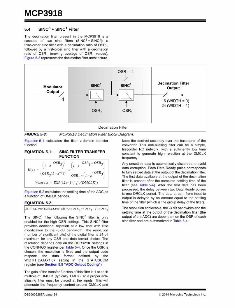
MCP3918
5.4 SINC3 + SINC1 Filter
The decimation filter present in the MCP3918 is acascade of two sinc filters (SINC3 + SINC1): athird-order sinc filter with a decimation ratio of OSR3,followed by a first-order sinc filter with a decimationratio of OSR1 (moving average of OSR1 values).Figure 5-3 represents the decimation filter architecture.
FIGURE 5-3: MCP3918 Decimation Filter Block Diagram.
Equation 5-1 calculates the filter z-domain transferfunction.
EQUATION 5-1: SINC FILTER TRANSFER FUNCTION
Equation 5-2 calculates the settling time of the ADC asa function of DMCLK periods.
EQUATION 5-2:
The SINC1 filter following the SINC3 filter is onlyenabled for the high OSR settings. This SINC1 filterprovides additional rejection at a low cost with littlemodification to the -3 dB bandwidth. The resolution(number of significant bits) of the digital filter is 24-bitmaximum for any OSR and data format choice. Theresolution depends only on the OSR<2:0> settings inthe CONFIG0 register per Table 5-4. Once the OSR ischosen, the resolution is fixed and the output coderespects the data format defined by theWIDTH_DATA<1:0> setting in the STATUSCOMregister (see Section 5.5 “ADC Output Coding”).
The gain of the transfer function of this filter is 1 at eachmultiple of DMCLK (typically 1 MHz), so a proper anti-aliasing filter must be placed at the inputs. This willattenuate the frequency content around DMCLK and
keep the desired accuracy over the baseband of theconverter. This anti-aliasing filter can be a simple,first-order RC network, with a sufficiently low timeconstant to generate high rejection at the DMCLKfrequency.Any unsettled data is automatically discarded to avoiddata corruption. Each Data Ready pulse correspondsto fully settled data at the output of the decimation filter.The first data available at the output of the decimationfilter is present after the complete settling time of thefilter (see Table 5-4). After the first data has beenprocessed, the delay between two Data Ready pulsesis one DRCLK period. The data stream from input tooutput is delayed by an amount equal to the settlingtime of the filter (which is the group delay of the filter).
The resolution achievable, the -3 dB bandwidth and thesettling time at the output of the decimation filter (theoutput of the ADC) are dependent on the OSR of eachsinc filter and are summarized in Table 5-4.
ModulatorOutput
SINC3 SINC1 Decimation FilterOutput
OSR3 OSR1
4 16 (WIDTH = 0)24 (WIDTH = 1)
Decimation Filter
OSR1 = 1
H z 1 z
- OSR3–
3
OSR3 1 z 1–– 3----------------------------------------------
1 z- OSR1 OSR3
–
OSR1 1 z- OSR3–
---------------------------------------------------------=
Where z EXP 2 j fin DMCLK =
SettlingTime DMCLKperiods 3 OSR3 OSR1 1– OSR3+=
DS20005287A-page 34 2014 Microchip Technology Inc.

MCP3918
FIGURE 5-4: Sinc Filter Frequency Response, OSR = 256, MCLK = 4 MHz, PRE<1:0> = 00.
FIGURE 5-5: Sinc Filter Frequency Response, OSR = 4096 (in pink), OSR = 512 (in blue), MCLK = 4 MHz, PRE<1:0> = 00.
5.5 ADC Output Coding
The second-order modulator, SINC3+SINC1 filter,PGA, VREF and the analog input structure all worktogether to produce the device transfer function for theanalog-to-digital conversion (see Equation 5-3).
The output data is calculated on 24-bit (23-bit plus sign)and coded in two's complement format, MSB first. Theoutput format can then be modified by theWIDTH_DATA<1:0> settings in the STATUSCOMregister to allow 16-, 24- or 32-bit formats compatibility(see Section 9.5 “STATUSCOM Register - Statusand Communication Register” for more information).
In case of positive saturation (CH0+ – CH0-> VREF/1.5), the output code is locked to 7FFFFF for
24-bit mode. In case of negative saturation(CH0+ - CH0- < -VREF/1.5), the output code is lockedto 800000 for 24-bit mode.
Equation 5-3 is only true for DC inputs. For AC inputs,this transfer function needs to be multiplied by thetransfer function of the SINC3+SINC1 filter (seeEquations 5-1 and 5-3).
EQUATION 5-3:
For data formats other than the default 24-bit format,Equation 5-3 should be multiplied by a scaling factor,depending on the data format used (defined byWIDTH_DATA<1:0>). The data format and theassociated scaling factors are given in Figure 5-6.
TABLE 5-4: OVERSAMPLING RATIO AND SINC FILTER SETTLING TIME
OSR<2:0> OSR3 OSR1 Total OSRResolution in Bits (No Missing Code)
Settling Time -3 dB Bandwidth
0 0 0 32 1 32 17 96/DMCLK 0.26*DRCLK
0 0 1 64 1 64 20 192/DMCLK 0.26*DRCLK
0 1 0 128 1 128 23 384/DMCLK 0.26*DRCLK
0 1 1 256 1 256 24 768/DMCLK 0.26*DRCLK
1 0 0 512 1 512 24 1536/DMCLK 0.26*DRCLK
1 0 1 512 2 1024 24 2048/DMCLK 0.37*DRCLK
1 1 0 512 4 2048 24 3072/DMCLK 0.42*DRCLK
1 1 1 512 8 4096 24 5120/DMCLK 0.43*DRCLK
-80
-60
-40
-20
0
agni
tude
(dB
)
-120
-100
1 10 100 1000 10000 100000
Ma
Input Frequency (Hz)
-100
-80
-60
-40
-20
0
gnitu
de (d
B)
-160
-140
-120
1 100 10000 1000000
Ma
Input Frequency (Hz)
For 24-bit Mode, WIDTH_DATA<1:0> = 01 (Default)
DATA_CH0CHn+ CHn-–
VREF+ VREF-–------------------------------------- 8 388 608 G 1.5=
2014 Microchip Technology Inc. DS20005287A-page 35
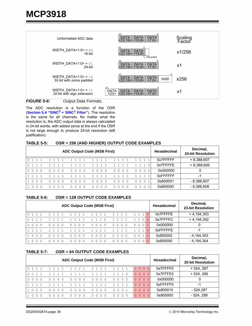
MCP3918
FIGURE 5-6: Output Data Formats.
The ADC resolution is a function of the OSR(Section 5.4 “SINC3 + SINC1 Filter”). The resolutionis the same for all channels. No matter what theresolution is, the ADC output data is always calculatedin 24-bit words, with added zeros at the end if the OSRis not large enough to produce 24-bit resolution (leftjustification).
DA
TA<7
>
WIDTH_DATA<1:0> = 1132-bit with sign extension
DATA<23>
DATA<23:16>
31 0DATA<15:8>
DATA<7:0>
WIDTH_DATA<1:0> = 1032-bit with zeros padded 0x00
31 0DATA
<23:16>DATA<7:0>
DATA<15:8>
WIDTH_DATA<1:0> = 0124-bit
DATA<23:16>
DATA<15:8>
DATA<7:0>
23 0
WIDTH_DATA<1:0> = 0016-bit
DATA<15:8>
15 0DATA
<23:16>Rounded
Unformatted ADC data DATA<23:16>
DATA<15:8>
DATA<7:0>
23 0
x1/256
x1
x256
x1
ScalingFactor
TABLE 5-5: OSR = 256 (AND HIGHER) OUTPUT CODE EXAMPLES
ADC Output Code (MSB First) HexadecimalDecimal,
24-bit Resolution
0 1 1 1 1 1 1 1 1 1 1 1 1 1 1 1 1 1 1 1 1 1 1 1 0x7FFFFF + 8,388,607
0 1 1 1 1 1 1 1 1 1 1 1 1 1 1 1 1 1 1 1 1 1 1 0 0x7FFFFE + 8,388,606
0 0 0 0 0 0 0 0 0 0 0 0 0 0 0 0 0 0 0 0 0 0 0 0 0x000000 0
1 1 1 1 1 1 1 1 1 1 1 1 1 1 1 1 1 1 1 1 1 1 1 1 0xFFFFFF -1
1 0 0 0 0 0 0 0 0 0 0 0 0 0 0 0 0 0 0 0 0 0 0 1 0x800001 - 8,388,607
1 0 0 0 0 0 0 0 0 0 0 0 0 0 0 0 0 0 0 0 0 0 0 0 0x800000 - 8,388,608
TABLE 5-6: OSR = 128 OUTPUT CODE EXAMPLES
ADC Output Code (MSB First) HexadecimalDecimal,
23-bit Resolution
0 1 1 1 1 1 1 1 1 1 1 1 1 1 1 1 1 1 1 1 1 1 1 0 0x7FFFFE + 4,194,303
0 1 1 1 1 1 1 1 1 1 1 1 1 1 1 0 1 1 1 1 1 1 0 0 0x7FFFFC + 4,194,302
0 0 0 0 0 0 0 0 0 0 0 0 0 0 0 0 0 0 0 0 0 0 0 0 0x000000 0
1 1 1 1 1 1 1 1 1 1 1 1 1 1 1 1 1 1 1 1 1 1 1 0 0xFFFFFE -1
1 0 0 0 0 0 0 0 0 0 0 0 0 0 0 0 0 0 0 0 0 0 1 0 0x800002 - 4,194,303
1 0 0 0 0 0 0 0 0 0 0 0 0 0 0 0 0 0 0 0 0 0 0 0 0x800000 - 4,194,304
TABLE 5-7: OSR = 64 OUTPUT CODE EXAMPLES
ADC Output Code (MSB First) HexadecimalDecimal,
20-bit Resolution
0 1 1 1 1 1 1 1 1 1 1 1 1 1 1 1 1 1 1 1 0 0 0 0 0x7FFFF0 + 524, 287
0 1 1 1 1 1 1 1 1 1 1 1 1 1 1 1 1 1 1 0 0 0 0 0 0x7FFFE0 + 524, 286
0 0 0 0 0 0 0 0 0 0 0 0 0 0 0 0 0 0 0 0 0 0 0 0 0x000000 0
1 1 1 1 1 1 1 1 1 1 1 1 1 1 1 1 1 1 1 1 0 0 0 0 0xFFFFF0 -1
1 0 0 0 0 0 0 0 0 0 0 0 0 0 0 0 0 0 0 1 0 0 0 0 0x800010 - 524,287
1 0 0 0 0 0 0 0 0 0 0 0 0 0 0 0 0 0 0 0 0 0 0 0 0x800000 - 524, 288
DS20005287A-page 36 2014 Microchip Technology Inc.

MCP3918
5.6 Voltage Reference
5.6.1 INTERNAL VOLTAGE REFERENCE
The MCP3918 contains an internal voltage referencesource specially designed to minimize drift overtemperature. In order to enable the internal voltagereference, the VREFEXT bit in the CONFIG1 registermust be set to ‘0’ (default mode). This internal VREFsupplies reference voltage to all channels. The typicalvalue of this voltage reference is 1.2V ± 2%. Theinternal reference has a very low typical temperaturecoefficient of ±7 ppm/°C, allowing the output to haveminimal variation, with respect to temperature, sincethey are proportional to (1/VREF).
The noise of the internal voltage reference is lowenough not to significantly degrade the SNR of theADC, if compared to a precision external low-noisevoltage reference. The output pin for the internalvoltage reference is REFIN+/OUT.
If the voltage reference is only used as an internalVREF, adding bypass capacitance on REFIN+/OUT isnot necessary for keeping ADC accuracy, but a minimal0.1 µF ceramic capacitance can be connected to avoidEMI/EMC susceptibility issues due to the antennacreated by the REFIN+/OUT pin, if left floating.
The bypass capacitors also help in applications wherethe voltage reference output is connected to othercircuits. In this case, additional buffering may beneeded, since the output drive capability of this outputis low.
Adding too much capacitance on the REFIN+/OUT pinmay slightly degrade the THD performance of the ADC.
5.6.2 DIFFERENTIAL EXTERNAL VOLTAGE INPUTS
When the VREFEXT bit is set to ‘1’, the two referencepins (REFIN+/OUT, REFIN-) become a differentialvoltage reference input. The voltage at theREFIN+/OUT is noted VREF+, and the voltage at theREFIN- pin is noted VREF-. The differential voltageinput value is given by Equation 5-4.
EQUATION 5-4:
The specified VREF ranges from 1.1V to 1.3V. TheREFIN- pin voltage (VREF-) should be limited to ±0.1V,with respect to AGND. Typically, for single-endedreference applications, the REFIN- pin should bedirectly connected to AGND, with its own separate trackto avoid any spike due to switching noise.
5.6.3 TEMPERATURE COMPENSATION (VREFCAL<7:0>)
The internal voltage reference consists of a proprietarycircuit and algorithm to compensate for first-order andsecond-order temperature coefficients. Thecompensation enables very low temperaturecoefficients (typically 9 ppm/°C) on the entire range oftemperatures, from - 40°C to +125°C. This temperaturecoefficient varies from part to part.
This temperature coefficient can be adjusted on eachpart through the VREFCAL<7:0> bits present in theCONFIG0 register (bits 7 to 0). These register settingsare only for advanced users. The VREFCAL<7:0> bitsshould not be modified unless the user wants tocalibrate the temperature coefficient of the wholesystem or application. The default value of this registeris set to 0x50. The default value (0x50) was chosen tooptimize the standard deviation of the tempco acrossprocess variation. The value can be slightly improvedto around 7 ppm/°C if the VREFCAL<7:0> bits arewritten at 0x42, but this setting degrades the standarddeviation of the VREF tempco.The typical variation ofthe temperature coefficient of the internal voltagereference with respect to the VREFCAL register codeis given by Figure 5-6. Modifying the value stored in theVREFCAL<7:0> bits may also vary the voltagereference, in addition to the temperature coefficient.
TABLE 5-8: OSR = 32 OUTPUT CODE EXAMPLES
ADC Output Code (MSB First) HexadecimalDecimal,
17-bit Resolution
0 1 1 1 1 1 1 1 1 1 1 1 1 1 1 1 1 0 0 0 0 0 0 0 0x7FFF80 + 65, 535
0 1 1 1 1 1 1 1 1 1 1 1 1 1 1 1 0 0 0 0 0 0 0 0 0x7FFF00 + 65, 534
0 0 0 0 0 0 0 0 0 0 0 0 0 0 0 0 0 0 0 0 0 0 0 0 0x000000 0
1 1 1 1 1 1 1 1 1 1 1 1 1 1 1 1 1 0 0 0 0 0 0 0 0xFFFF80 -1
1 0 0 0 0 0 0 0 0 0 0 0 0 0 0 0 1 0 0 0 0 0 0 0 0x800080 - 65,535
1 0 0 0 0 0 0 0 0 0 0 0 0 0 0 0 0 0 0 0 0 0 0 0 0x800000 - 65, 536
VREF = VREF+ – VREF-
2014 Microchip Technology Inc. DS20005287A-page 37
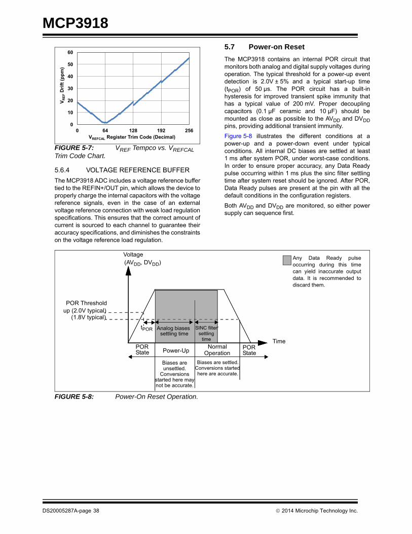
MCP3918
DS
FIGURE 5-7: VREF Tempco vs. VREFCAL Trim Code Chart.
5.6.4 VOLTAGE REFERENCE BUFFER
The MCP3918 ADC includes a voltage reference buffertied to the REFIN+/OUT pin, which allows the device toproperly charge the internal capacitors with the voltagereference signals, even in the case of an externalvoltage reference connection with weak load regulationspecifications. This ensures that the correct amount ofcurrent is sourced to each channel to guarantee theiraccuracy specifications, and diminishes the constraintson the voltage reference load regulation.
5.7 Power-on Reset
The MCP3918 contains an internal POR circuit thatmonitors both analog and digital supply voltages duringoperation. The typical threshold for a power-up eventdetection is 2.0V ± 5% and a typical start-up time(tPOR) of 50 µs. The POR circuit has a built-inhysteresis for improved transient spike immunity thathas a typical value of 200 mV. Proper decouplingcapacitors (0.1 µF ceramic and 10 µF) should bemounted as close as possible to the AVDD and DVDDpins, providing additional transient immunity.
Figure 5-8 illustrates the different conditions at apower-up and a power-down event under typicalconditions. All internal DC biases are settled at least1 ms after system POR, under worst-case conditions.In order to ensure proper accuracy, any Data Readypulse occurring within 1 ms plus the sinc filter settlingtime after system reset should be ignored. After POR,Data Ready pulses are present at the pin with all thedefault conditions in the configuration registers.
Both AVDD and DVDD are monitored, so either powersupply can sequence first.
FIGURE 5-8: Power-On Reset Operation.
0
10
20
30
40
50
60
0 64 128 192 256
V REF
Drif
t (pp
m)
VREFCAL Register Trim Code (Decimal)
PORState Power-Up
Normal PORState
Biases areunsettled.
Conversionsstarted here maynot be accurate.
Biases are settled.Conversions startedhere are accurate.
Analog biasessettling time
SINC filtersettling
time
Voltage
Time
POR Thresholdup (2.0V typical)
(1.8V typical)
tPOR
Operation
Analog biasessettling time
SINC filtersettling
time
(AVDD, DVDD)Any Data Ready pulseoccurring during this timecan yield inaccurate outputdata. It is recommended todiscard them.
20005287A-page 38 2014 Microchip Technology Inc.
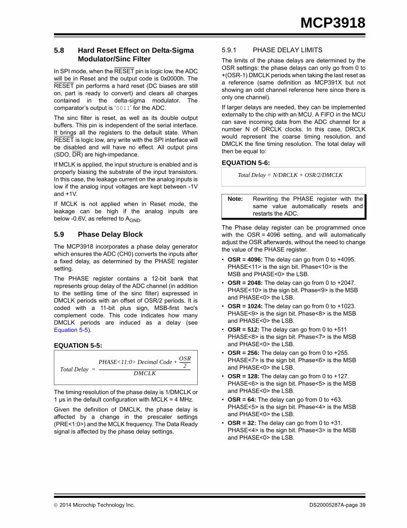
MCP3918
5.8 Hard Reset Effect on Delta-Sigma Modulator/Sinc Filter
In SPI mode, when the RESET pin is logic low, the ADCwill be in Reset and the output code is 0x0000h. TheRESET pin performs a hard reset (DC biases are stillon, part is ready to convert) and clears all chargescontained in the delta-sigma modulator. Thecomparator’s output is ‘0011’ for the ADC.
The sinc filter is reset, as well as its double outputbuffers. This pin is independent of the serial interface.It brings all the registers to the default state. WhenRESET is logic low, any write with the SPI interface willbe disabled and will have no effect. All output pins(SDO, DR) are high-impedance.
If MCLK is applied, the input structure is enabled and isproperly biasing the substrate of the input transistors.In this case, the leakage current on the analog inputs islow if the analog input voltages are kept between -1Vand +1V.
If MCLK is not applied when in Reset mode, theleakage can be high if the analog inputs arebelow -0.6V, as referred to AGND.
5.9 Phase Delay Block
The MCP3918 incorporates a phase delay generatorwhich ensures the ADC (CH0) converts the inputs aftera fixed delay, as determined by the PHASE registersetting.
The PHASE register contains a 12-bit bank thatrepresents group delay of the ADC channel (in additionto the settling time of the sinc filter) expressed inDMCLK periods with an offset of OSR/2 periods. It iscoded with a 11-bit plus sign, MSB-first two'scomplement code. This code indicates how manyDMCLK periods are induced as a delay (seeEquation 5-5).
EQUATION 5-5:
The timing resolution of the phase delay is 1/DMCLK or1 µs in the default configuration with MCLK = 4 MHz.
Given the definition of DMCLK, the phase delay isaffected by a change in the prescaler settings(PRE<1:0>) and the MCLK frequency. The Data Readysignal is affected by the phase delay settings.
5.9.1 PHASE DELAY LIMITS
The limits of the phase delays are determined by theOSR settings: the phase delays can only go from 0 to+(OSR-1) DMCLK periods when taking the last reset asa reference (same definition as MCP391X but notshowing an odd channel reference here since there isonly one channel).
If larger delays are needed, they can be implementedexternally to the chip with an MCU. A FIFO in the MCUcan save incoming data from the ADC channel for anumber N of DRCLK clocks. In this case, DRCLKwould represent the coarse timing resolution, andDMCLK the fine timing resolution. The total delay willthen be equal to:
EQUATION 5-6:
The Phase delay register can be programmed oncewith the OSR = 4096 setting, and will automaticallyadjust the OSR afterwards, without the need to changethe value of the PHASE register.
• OSR = 4096: The delay can go from 0 to +4095. PHASE<11> is the sign bit. Phase<10> is the MSB and PHASE<0> the LSB.
• OSR = 2048: The delay can go from 0 to +2047. PHASE<10> is the sign bit. Phase<9> is the MSB and PHASE<0> the LSB.
• OSR = 1024: The delay can go from 0 to +1023. PHASE<9> is the sign bit. Phase<8> is the MSB and PHASE<0> the LSB.
• OSR = 512: The delay can go from 0 to +511 PHASE<8> is the sign bit. Phase<7> is the MSB and PHASE<0> the LSB.
• OSR = 256: The delay can go from 0 to +255. PHASE<7> is the sign bit. Phase<6> is the MSB and PHASE<0> the LSB.
• OSR = 128: The delay can go from 0 to +127. PHASE<6> is the sign bit. Phase<5> is the MSB and PHASE<0> the LSB.
• OSR = 64: The delay can go from 0 to +63. PHASE<5> is the sign bit. Phase<4> is the MSB and PHASE<0> the LSB.
• OSR = 32: The delay can go from 0 to +31. PHASE<4> is the sign bit. Phase<3> is the MSB and PHASE<0> the LSB.
Total DelayPHASE<11:0> Decimal Code
OSR2
-----------+
DMCLK--------------------------------------------------------------------------------------------=
Note: Rewriting the PHASE register with thesame value automatically resets andrestarts the ADC.
Total Delay = N/DRCLK + OSR/2/DMCLK
2014 Microchip Technology Inc. DS20005287A-page 39
MCP3918
5.10 Data Ready Status BitIn addition to the DR pin indicator, the MCP3918 deviceincludes a separate Data Ready status bit. The ADCchannel is associated to the correspondingDRSTATUS bit that can be read at all times in theSTATUSCOM register. This status bit can be used tosynchronize the data retrieval, in case the DR pin is notconnected (see Section 6.8 “ADC Channel Latchingand Synchronization”).
The DRSTATUS bit is not writable; writing on it has noeffect. It has a default value of '1', which indicates thatthe data of the corresponding ADC is not ready. Thismeans that the ADC output register has not beenupdated since the last reading (or since the last reset).The DRSTATUS bit takes the '0' state, once the ADCchannel register is updated (which happens at aDRCLK rate). A simple read of the STATUSCOMregister clears the DRSTATUS bit to its default value('1').
5.11 Crystal Oscillator
The MCP3918 includes a Pierce-type crystal oscillatorwith very high stability and ensures very low tempcoand jitter for the clock generation. This oscillator canhandle crystal frequencies up to 20 MHz, provided thatproper load capacitances and quartz quality factor areused. The crystal oscillator is enabled whenCLKEXT = 0 in the CONFIG1 register, therefore itcannot be enabled during the 2-Wire Interface mode. Itis only selectable in the SPI Mode.
For a proper start-up, the load capacitors of the crystalshould be connected between OSC1 and DGND andbetween OSC2 and DGND. They should also respectEquation 5-7.
EQUATION 5-7:
When CLKEXT = 1, the crystal oscillator is bypassedby a digital buffer, to allow direct clock input for anexternal clock (see Figure 4-1). In this case, OSC2becomes the MODE select input pin for the Interfacemode. When MODE = 0, the digital interface stays inSPI mode; when MODE = 1, the digital interfacetoggles to the 2-Wire mode. A pull-down current forcesthe MODE to be logic low (SPI mode) by default if theOSC2 pin is floating.
For proper operation, the external clock should not behigher than 20 MHz before prescaling(MCLK < 20 MHz).
TABLE 5-9: PHASE VALUES WITHMCLK = 4 MHZ, OSR = 4096, PRE<1:0> = 00
PHASE<11:0> Hex Delay
0 1 1 1 1 1 1 1 1 1 1 1 0x7FF 4095 µs
0 1 1 1 1 1 1 1 1 1 1 0 0x7FE 4094 µs
0 0 0 0 0 0 0 0 0 0 0 1 0x001 2049 µs
0 0 0 0 0 0 0 0 0 0 0 0 0x000 2048 µs
1 1 1 1 1 1 1 1 1 1 1 1 0xFFF 2047 µs
1 0 0 0 0 0 0 0 0 0 0 1 0x801 1 µs
1 0 0 0 0 0 0 0 0 0 0 0 0x800 0 µs
Note: In addition to the conditions defining themaximum MCLK input frequency range,the AMCLK frequency should bemaintained inferior to the maximum limitsdefined in Table 5-2, to ensure theaccuracy of the ADC. If these limits areexceeded, it is recommended to chooseeither a larger OSR or a larger prescalervalue so that AMCLK can respect theselimits.
RM 1.6 106 1
f C LOAD-------------------------
2<
Where:
f = crystal frequency in MHz
CLOAD = load capacitance in pF, including parasitics from the PCB
RM = motional resistance of the quartz, in ohms
DS20005287A-page 40 2014 Microchip Technology Inc.

MCP3918
5.12 Digital System Offset and Gain Errors
The MCP3918 incorporates two sets of additionalregisters to perform system digital offset and gain errorcalibration, which will modify the output result of thechannel, if calibration is enabled. The gain and offsetcalibrations can be enabled or disabled through twoconfiguration bits (EN_OFFCAL and EN_GAINCAL).When both calibrations are enabled, the output of theADC is modified per Equation 5-8. These calibrationsare not effective in 2-Wire interface mode.
EQUATION 5-8: DIGITAL OFFSET AND GAIN ERROR CALIBRATION REGISTERS CALCULATIONS
5.12.1 DIGITAL OFFSET ERROR CALIBRATION
The OFFCAL_CH0 register is 23-bit plus sign two’scomplement registers, whose LSB value is the same asthe Channel ADC Data. This register is then added bitby bit to the ADC output codes, if the EN_OFFCAL bitis enabled. Enabling the EN_OFFCAL bit does notcreate a pipeline delay; the offset addition isinstantaneous. For low OSR values, only the significantdigits are added to the output (up to the resolution ofthe ADC; for example, at OSR = 32, only the first 17bits are added).
The offset is not added when the correspondingchannel is in Reset or Shutdown mode. Thecorresponding input voltage offset value added by eachLSB in these 24-bit registers is:
EQUATION 5-9:
This register is a “Don't Care” if EN_OFFCAL = 0(offset calibration disabled), but its value is not clearedby the EN_OFFCAL bit.
5.12.2 DIGITAL GAIN ERROR CALIBRATION
This register is a signed 24-bit MSB – first registercoded with a range of -1x to +(1 - 2-23)x (from0x800000 to 0x7FFFFF). The gain calibration adds 1xto this register and multiplies it to the output code of thechannel bit by bit, after offset calibration. Thus, the gaincalibration ranges from 0x to 1.9999999x (from0x80000 to 0x7FFFFF). The LSB corresponds to a 2-23
increment in the multiplier.
Enabling EN_GAINCAL creates a pipeline delay of24 DMCLK periods on all channels. All Data Readypulses are delayed by 24 DMCLK periods, startingfrom data ready pulse following the command enablingEN_GAINCAL bit. The gain calibration is effective onthe next data ready pulse following the commandenabling EN_GAINCAL bit.
The digital gain calibration does not function when thecorresponding channel is in Reset or Shutdown mode.The gain multiplier value for an LSB in this 24-bitregister is:
EQUATION 5-10:
This register is a “Don't Care” if EN_GAINCAL = 0(offset calibration disabled), but its value is not clearedby the EN_GAINCAL bit.
The output data is kept to either 7FFF or 8000 (16-bitmode) or 7FFFFF or 800000 (24-bit mode) if the outputresults are out of bounds after all calibrations areperformed.
DATA_CH0 post cal– DATA_CH0 pre cal– OFFCAL_CH0+ 1 GAINCAL_CH0+ =
OFFSET(1LSB) = VREF/(PGA_CHn x 1.5 x 8388608)
GAIN (1LSB) = 1/8388608
2014 Microchip Technology Inc. DS20005287A-page 41

MCP3918
NOTES:
DS20005287A-page 42 2014 Microchip Technology Inc.
MCP3918
6.0 SPI SERIAL INTERFACE DESCRIPTION
6.1 Overview
The MCP3918 device includes a four-wire (CS, SCK,SDI, SDO) digital serial interface that is compatible withSPI Modes 0,0 and 1,1. Data is clocked out of theMCP3918 on the falling edge of SCK, and data isclocked into the MCP3918 on the rising edge of SCK.In these modes, the SCK clock can idle either high (1,1)or low (0,0). The digital interface is asynchronous withthe MCLK clock that controls the ADC sampling anddigital filtering. All the digital input pins areSchmitt-triggered to avoid system noise perturbationson the communications.
Each independent SPI communication starts with a CSfalling edge and stops with the CS rising edge. WhenCS is logic high, SDO is in high-impedance, there aretransitions on SCK, and SDI has no effect. Changingfrom an SPI Mode 1,1 to an SPI Mode 0,0 and viceversa is possible and can be done while the CS pin islogic high. Any CS rising edge clears thecommunication and resets the SPI digital interface.
Additional control pins (RESET, DR) are also providedon separate pins for advanced communicationfeatures. The Data Ready pin (DR) outputs pulseswhen a new ADC channel data is available for reading,which can be used as an interrupt for an MCU. Themaster reset pin (RESET) acts like a hard reset andcan reset the part to its default power-up configuration(equivalent to a POR state).
The MCP3918 interface has a simple commandstructure. Every command is either a Read commandfrom a register or a Write command to a register. TheMCP3918 device includes nine registers defined in theregister map in Table 9-1. The register map is fullycompatible with the MCP391X family to allow easyporting of MCU code from one design to another insidethe MCP391X family. The first byte (8-bit wide)transmitted is always the Control byte that defines theaddress of the register and the type of command (Reador Write). It is followed by the register itself, which canbe in a 16-, 24- or 32-bit format, depending on themultiple format settings defined in the STATUSCOMregister. The MCP3918 is compatible with multipleformats that help reduce overhead in the data handlingfor most MCUs and processors available on the market(8-, 16- or 32-bit MCUs) and improve MCU-codecompaction and efficiency.
The MCP3918 digital interface is capable of handlingvarious continuous read and write modes, which allowthe device to perform ADC data streaming or fullregister map writing within only one communication(and therefore with only one unique Control byte). Theinternal registers can be grouped together with variousconfigurations through the READ<1:0> and WRITEbits. The internal address counter of the serial interfacecan be automatically incremented with no additionalControl byte needed, in order to loop through thevarious groups of registers within the register map. Thegroups are defined in Table 9-2.
The MCP3918 device also includes advanced securityfeatures to secure each communication, to avoidprocessing unwanted write commands in order tochange the desired configuration, and to alert the userin case of a change in the desired configuration.
Each SPI read communication can be secured througha selectable CRC-16 checksum provided on the SDOpin at the end of every communication sequence. ThisCRC-16 computation is compatible with the DMA CRChardware of the PIC24 and PIC32 MCUs, resulting inno additional overhead for added security.
In order to secure the entire configuration of the device,the MCP3918 includes an 8-bit lock code(LOCK<7:0>), which blocks all write commands to thefull register map if the value of the LOCK<7:0> is notequal to a defined password (0xA5). The user canprotect its configuration by changing the LOCK<7:0>value to 0x00 after the full programming, so that nounwanted write command will result in a change in theconfiguration (because LOCK<7:0> is different fromthe 0xA5 password).
An additional CRC-16 calculation is also runningcontinuously in the background to ensure the integrityof the full register map. All writable registers of theregister map (except for the MOD register) areprocessed through a CRC-16 calculation engine andgive a CRC-16 checksum that depends on theconfiguration. This checksum is readable on theLOCK/CRC register and updated at all times. If achange in this checksum occurs, a selectable interruptcan give a flag on the DR pin (the DR pin becomes logiclow) to warn the user that the configuration iscorrupted.
2014 Microchip Technology Inc. DS20005287A-page 43

MCP3918
6.2 Control Byte
The Control byte of the MCP3918 contains two deviceAddress bits (A<6:5>), five register Address bits(A<4:0>) and a Read/Write bit (R/W). The first bytetransmitted to the MCP3918 in any communication isalways the Control byte. During the Control bytetransfer, the SDO pin is always in a high-impedancestate. The MCP3918 interface is device addressable(through A<6:5>), so that multiple chips can be presenton the same SPI bus with no data bus contention, evenif they use the same CS pin and a provided half-duplexSPI interface, with a different address identifier. Thisfunctionality enables, for example, a Serial EEPROMlike 24AAXXX/24LCXXX or 24FCXXX. Moreover, itenables the MCP3918 to share all the SPI pins and toconsume less I/O pins in the application processor,since all these Serial EEPROM circuits useA<6:5> = 00.
FIGURE 6-1: Control Byte.
The default device address bits are A<6:5> = 01(contact the Microchip factory for other available deviceaddress bits). For more information, see the ProductIdentification System section. The register map isdefined in Table 9-1.
6.3 Reading from the Device
The first register read on the SDO pin is the one definedby the address (A<4:0>) given in the Control byte. Afterthis first register is fully transmitted, if the CS pin ismaintained logic low, the communication continueswithout an additional Control byte and the SDO pintransmits another register with the addressautomatically incremented.
Four different read mode configurations can be definedthrough the READ<1:0> bits in the STATUSCOMregister for the address increment (see Section 6.5“Continuous Communications, Looping onRegister Sets” and Table 9-2). The data on SDO isclocked out of the MCP3918 on the falling edge ofSCK. The reading format for each register is defined inSection 5.5 “ADC Output Coding”.
FIGURE 6-2: Read on a Single Register with 24-bit Format (WIDTH_DATA<1:0> = 01, SPI Mode 1,1).
A<6> A<5> A<4> A<3> A<2> A<1> A<0> R/W
Device Address
Register Address Read/Write
READ Communication (SPI mode 1,1)
Don’t careDon’t care
A<6
>
DA
TA<2
2>
SCK
SDI
SDO
A<5
>
A<4
>
A<3
>
A<2
>
A<1
>
A<0
>
CS
DA
TA<2
1>
DA
TA<2
0>
DA
TA<1
9>
DA
TA<1
8>
DA
TA<1
7>
DA
TA<1
6>
DA
TA<1
5>
DA
TA<1
4>
DA
TA<1
3>
DA
TA<1
2>
DA
TA<1
1>
DA
TA<1
0>
DA
TA<9
>
DA
TA<8
>
DA
TA<7
>
DA
TA<6
>
DA
TA<5
>
DA
TA<4
>
DA
TA<3
>
DA
TA<2
>
DA
TA<1
>
DATA<0>Hi-Z Hi-Z
Device latches SDI on rising edge Device latches SDO on falling edge
R/W
DA
TA<2
3>High Z High Z
DS20005287A-page 44 2014 Microchip Technology Inc.
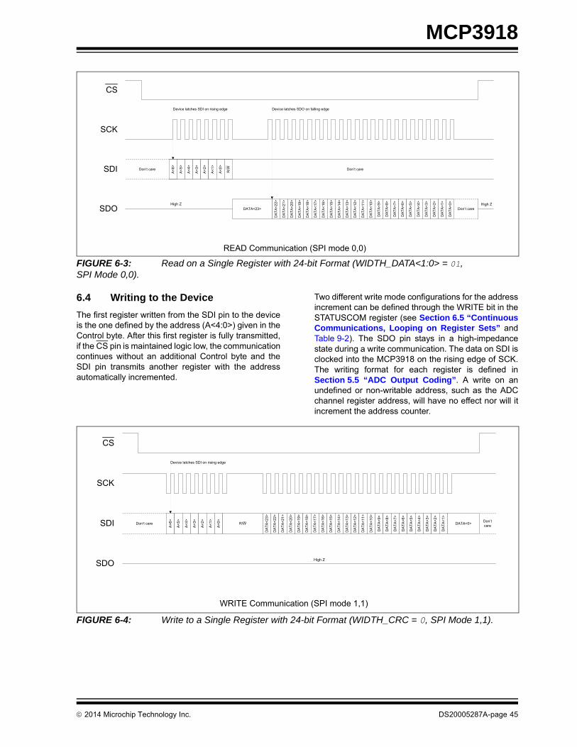
MCP3918
FIGURE 6-3: Read on a Single Register with 24-bit Format (WIDTH_DATA<1:0> = 01, SPI Mode 0,0).
6.4 Writing to the Device
The first register written from the SDI pin to the deviceis the one defined by the address (A<4:0>) given in theControl byte. After this first register is fully transmitted,if the CS pin is maintained logic low, the communicationcontinues without an additional Control byte and theSDI pin transmits another register with the addressautomatically incremented.
Two different write mode configurations for the addressincrement can be defined through the WRITE bit in theSTATUSCOM register (see Section 6.5 “ContinuousCommunications, Looping on Register Sets” andTable 9-2). The SDO pin stays in a high-impedancestate during a write communication. The data on SDI isclocked into the MCP3918 on the rising edge of SCK.The writing format for each register is defined inSection 5.5 “ADC Output Coding”. A write on anundefined or non-writable address, such as the ADCchannel register address, will have no effect nor will itincrement the address counter.
FIGURE 6-4: Write to a Single Register with 24-bit Format (WIDTH_CRC = 0, SPI Mode 1,1).
READ Communication (SPI mode 0,0)
Don’t careDon’t care
Don’t care
A<6
>
DA
TA<2
2>
SCK
SDI
SDO
A<5
>
A<4
>
A<3
>
A<2
>
A<1
>
A<0
>
R/W
CS
DATA<23>
DA
TA<2
1>
DA
TA<2
0>
DA
TA<1
9>
DA
TA<1
8>
DA
TA<1
7>
DA
TA<1
6>
DA
TA<1
5>
DA
TA<1
4>
DA
TA<1
3>
DA
TA<1
2>
DA
TA<1
1>
DA
TA<1
0>
DA
TA<9
>
DA
TA<8
>
DA
TA<7
>
DA
TA<6
>
DA
TA<5
>
DA
TA<4
>
DA
TA<3
>
DA
TA<2
>
DA
TA<1
>
DA
TA<0
>
Hi-Z Hi-Z
Device latches SDI on rising edge Device latches SDO on falling edge
High Z High Z
WRITE Communication (SPI mode 1,1)
Don’t care
A<6
>
SCK
SDI
SDO
A<5
>
A<4
>
A<3
>
A<2
>
A<1
>
A<0
>
CS
Hi-Z
Device latches SDI on rising edge
R/W
DA
TA<2
2>
DA
TA<2
1>
DA
TA<2
0>
DA
TA<1
9>
DA
TA<1
8>
DA
TA<1
7>
DA
TA<1
6>
DA
TA<1
5>
DA
TA<1
4>
DA
TA<1
3>
DA
TA<1
2>
DA
TA<1
1>
DA
TA<1
0>
DA
TA<9
>
DA
TA<8
>
DA
TA<7
>
DA
TA<6
>
DA
TA<5
>
DA
TA<4
>
DA
TA<3
>
DA
TA<2
>
DA
TA<1
>
DA
TA<2
3>
Don’t careDATA<0>
High Z
2014 Microchip Technology Inc. DS20005287A-page 45

MCP3918
FIGURE 6-5: Write to a Single Register with 24-bit Format (WIDTH_CRC = 0, SPI Mode 0,0).
WRITE Communication (SPI mode 0,0)
Don’t care
A<6
>
SCK
SDI
SDO
A<5
>
A<4
>
A<3
>
A<2
>
A<1
>
A<0
>
R/W
CS
Hi-Z
Device latches SDI on rising edge
Don’t care
DA
TA<2
2>
DATA<23>
DA
TA<2
1>
DA
TA<2
0>
DA
TA<1
9>
DA
TA<1
8>
DA
TA<1
7>
DA
TA<1
6>
DA
TA<1
5>
DA
TA<1
4>
DA
TA<1
3>
DA
TA<1
2>
DA
TA<1
1>
DA
TA<1
0>
DA
TA<9
>
DA
TA<8
>
DA
TA<7
>
DA
TA<6
>
DA
TA<5
>
DA
TA<4
>
DA
TA<3
>
DA
TA<2
>
DA
TA<1
>
DA
TA<0
>
High Z
DS20005287A-page 46 2014 Microchip Technology Inc.

MCP3918
6.5 Continuous Communications, Looping on Register Sets
The MCP3918 digital interface can processcommunications in Continuous mode, without havingto enter an SPI command between each read or writeto a register. This feature allows the user to reducecommunication overhead to the strict minimum, whichdiminishes EMI emissions and reduces switching noisein the system.
The registers can be grouped into multiple sets forcontinuous communications. The grouping of theregisters in the different sets is defined by theREAD<1:0> and WRITE bits that control the internalSPI communication address pointer. For a graphicalrepresentation of the register map sets in the functionof the READ<1:0> and WRITE bits, please seeTable 9-2.
In the case of a continuous communication, there isonly one Control byte on SDI to start thecommunication after a CS pin falling edge. The partstays within the same communication loop until the CS
pin returns logic high. The SPI internal register addresspointer starts by transmitting/receiving the addressdefined in the Control byte. After this firsttransmission/reception, the SPI internal registeraddress pointer automatically increments to the nextavailable address in the register set for eachtransmission/reception. When it reaches the lastaddress in the set, the communication sequence isfinished. The address pointer loops automatically backto the first address of the defined set and restarts a newsequence with auto-increment (see Table 6-6). Theundefined or unused addresses are automaticallyjumped by the address pointer (they are not consideredto be part of the register map by the address pointer).This internal address pointer automatic selectionallows the following functionality:
• Read one ADC channel data continuously
• Continuously read the entire register map
• Continuously read or write each separate register
• Continuously read or write all configuration registers
FIGURE 6-6: Continuous Communication Sequences.
Continuous READ communication (24-bit format)
Don’t care
SCK
SDI
SDO
CS
Hi-Z
8x
CONTROLBYTE
24x
ADDR ... ADDR + n
Starts read sequenceat address ADDR
Complete READ sequence
ADDR + 1
24x ... 24x 24x
ADDR ...
Complete READ sequence
ADDR + 1
24x ... 24x
ADDR + n
Continuous WRITE communication (24-bit format)
Don’t care
SCK
SDI
SDO
CS
Hi-Z
8x
CONTROLBYTE
24x
ADDR ... ADDR + n
Starts write sequenceat address ADDR
Complete WRITE sequence
ADDR + 1
24x ... 24x 24x
ADDR ...
Complete WRITE sequence
ADDR + 1
24x ... 24x
ADDR + n
Don’t care
ADDR
ADDR + 1
...
ADDR + n
CompleteREADsequence
Roll-over
ADDRESS SET
ADDR
ADDR + 1
...
ADDR + n
CompleteWRITEsequence
Roll-over
ADDRESS SET
High Z
High Z
2014 Microchip Technology Inc. DS20005287A-page 47
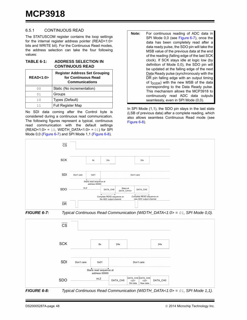
MCP3918
6.5.1 CONTINUOUS READ
The STATUSCOM register contains the loop settingsfor the internal register address pointer (READ<1:0>bits and WRITE bit). For the Continuous Read modes,the address selection can take the four followingvalues:
No SDI data coming after the Control byte isconsidered during a continuous read communication.The following figures represent a typical, continuousread communication with the default settings(READ<1:0> = 10, WIDTH_DATA<1:0> = 01) for SPIMode 0,0 (Figure 6-7) and SPI Mode 1,1 (Figure 6-8).
In SPI Mode (1,1), the SDO pin stays in the last state(LSB of previous data) after a complete reading, whichalso allows seamless Continuous Read mode (seeFigure 6-8).
FIGURE 6-7: Typical Continuous Read Communication (WIDTH_DATA<1:0> = 01, SPI Mode 0,0).
FIGURE 6-8: Typical Continuous Read Communication (WIDTH_DATA<1:0> = 01, SPI Mode 1,1).
TABLE 6-1: ADDRESS SELECTION IN CONTINUOUS READ
READ<1:0>Register Address Set Grouping
for Continuous Read Communications
00 Static (No incrementation)
01 Groups
10 Types (Default)
11 Full Register Map
Note: For continuous reading of ADC data inSPI Mode 0,0 (see Figure 6-7), once thedata has been completely read after adata ready pulse, the SDO pin will take theMSB value of the previous data at the endof the reading (falling edge of the last SCKclock). If SCK stays idle at logic low (bydefinition of Mode 0,0), the SDO pin willbe updated at the falling edge of the nextData Ready pulse (synchronously with theDR pin falling edge with an output timingof tDODR) with the new MSB of the datacorresponding to the Data Ready pulse.This mechanism allows the MCP3918 tocontinuously read ADC data outputsseamlessly, even in SPI Mode (0,0).
Don’t care
SCK
SDI
SDO
CS
Hi-Z
8x
0x01
24x
Starts read sequence at address 00000
24x
Don’t care
DR
Complete READ sequence onnew ADC output channel
Complete READ sequence on the ADC output channel
DATA_CH0Stays at DATA_CH<0>DATA_CH0
Don’t care
SCK
SDI
SDO
CS
Hi-Z
8x
0x01
24x
Starts read sequence at address 00000
24x
Don’t care
DATA_CH0 DATA_CH0DATA_CH0
<23> New data
DATA_CH0<23>
Old data
DS20005287A-page 48 2014 Microchip Technology Inc.
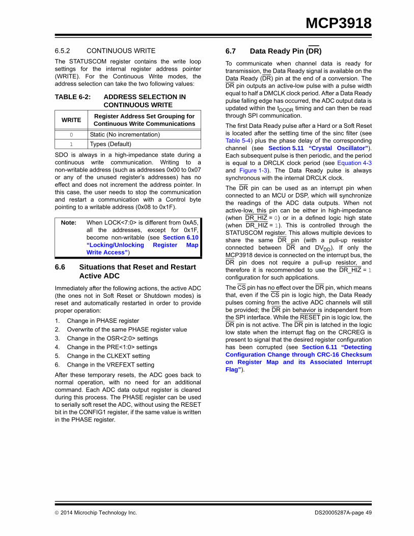
MCP3918
6.5.2 CONTINUOUS WRITE
The STATUSCOM register contains the write loopsettings for the internal register address pointer(WRITE). For the Continuous Write modes, theaddress selection can take the two following values:
SDO is always in a high-impedance state during acontinuous write communication. Writing to anon-writable address (such as addresses 0x00 to 0x07or any of the unused register’s addresses) has noeffect and does not increment the address pointer. Inthis case, the user needs to stop the communicationand restart a communication with a Control bytepointing to a writable address (0x08 to 0x1F).
6.6 Situations that Reset and Restart Active ADC
Immediately after the following actions, the active ADC(the ones not in Soft Reset or Shutdown modes) isreset and automatically restarted in order to provideproper operation:
1. Change in PHASE register
2. Overwrite of the same PHASE register value
3. Change in the OSR<2:0> settings
4. Change in the PRE<1:0> settings
5. Change in the CLKEXT setting
6. Change in the VREFEXT setting
After these temporary resets, the ADC goes back tonormal operation, with no need for an additionalcommand. Each ADC data output register is clearedduring this process. The PHASE register can be usedto serially soft reset the ADC, without using the RESETbit in the CONFIG1 register, if the same value is writtenin the PHASE register.
6.7 Data Ready Pin (DR)
To communicate when channel data is ready fortransmission, the Data Ready signal is available on theData Ready (DR) pin at the end of a conversion. TheDR pin outputs an active-low pulse with a pulse widthequal to half a DMCLK clock period. After a Data Readypulse falling edge has occurred, the ADC output data isupdated within the tDODR timing and can then be readthrough SPI communication.
The first Data Ready pulse after a Hard or a Soft Resetis located after the settling time of the sinc filter (seeTable 5-4) plus the phase delay of the correspondingchannel (see Section 5.11 “Crystal Oscillator”).Each subsequent pulse is then periodic, and the periodis equal to a DRCLK clock period (see Equation 4-3and Figure 1-3). The Data Ready pulse is alwayssynchronous with the internal DRCLK clock.
The DR pin can be used as an interrupt pin whenconnected to an MCU or DSP, which will synchronizethe readings of the ADC data outputs. When notactive-low, this pin can be either in high-impedance(when DR_HIZ = 0) or in a defined logic high state(when DR_HIZ = 1). This is controlled through theSTATUSCOM register. This allows multiple devices toshare the same DR pin (with a pull-up resistorconnected between DR and DVDD). If only theMCP3918 device is connected on the interrupt bus, theDR pin does not require a pull-up resistor, andtherefore it is recommended to use the DR_HIZ = 1configuration for such applications.
The CS pin has no effect over the DR pin, which meansthat, even if the CS pin is logic high, the Data Readypulses coming from the active ADC channels will stillbe provided; the DR pin behavior is independent fromthe SPI interface. While the RESET pin is logic low, theDR pin is not active. The DR pin is latched in the logiclow state when the interrupt flag on the CRCREG ispresent to signal that the desired register configurationhas been corrupted (see Section 6.11 “DetectingConfiguration Change through CRC-16 Checksumon Register Map and its Associated InterruptFlag”).
TABLE 6-2: ADDRESS SELECTION IN CONTINUOUS WRITE
WRITERegister Address Set Grouping for Continuous Write Communications
0 Static (No incrementation)
1 Types (Default)
Note: When LOCK<7:0> is different from 0xA5,all the addresses, except for 0x1F,become non-writable (see Section 6.10“Locking/Unlocking Register MapWrite Access”)
2014 Microchip Technology Inc. DS20005287A-page 49

MCP3918
6.8 ADC Channel Latching and Synchronization
The ADC data output register (address 0x00) has adouble buffer output structure. The two sets of latchesin series are triggered by the data ready signal and aninternal signal indicating the beginning of a readcommunication sequence (read start).
The first set of latches holds the ADC channel dataoutput register when the data is ready. This behavior issynchronous with the MCLK clock.
The second set of latches ensures that, when readingstarts on an ADC output, the corresponding data islatched, so that no data corruption can occur within aread. This behavior is synchronous with the SCK clock.If an ADC read has started, in order to read thefollowing ADC output, the current reading needs to befully completed (all bits must be read on the SDO pinfrom the ADC output data registers).
Since the double output buffer structure is triggeredwith two events that depend on two asynchronousclocks (data ready pulse with MCLK and read start withSCK), it is recommended to implement one of the threefollowing methods on the MCU or the processor, inorder to synchronize the reading of the channels:
1. Use the DR pin pulses as an interrupt: once afalling edge occurs on the DR pin, the data isavailable for reading on the ADC outputregisters after the tDODR timing. If this timing isnot respected, data corruption can occur.
2. Use a timer clocked with MCLK as asynchronization event: since the data readypulse is synchronous with MCLK, the user cancalculate the position of the data ready pulsedepending on the PHASE, the OSR<2:0> andthe PRE<1:0> settings. Again, the tDODR timingneeds to be added to this calculation, to avoiddata corruption.
3. Poll the DRSTATUS bit in the STATUSCOMregister: this method consists of continuouslyreading the STATUSCOM register and waitingfor the DRSTATUS bit to be equal to '0'. Whenthis event happens, the user can start a newcommunication to read the desired ADC data. Inthis case, no additional timing is required.
The first method is the preferred one, as it can be usedwithout adding additional MCU code space, butrequires connecting the DR pin to an I/O pin of theMCU. The two last methods require more MCU codespace and execution time, but they allow synchronizingthe reading of the channels without connecting the DRpin, which saves one I/O pin on the MCU.
6.9 Securing Read Communications through CRC-16 Checksum
Since power/energy metering systems can generate orreceive large EMI/EMC interferences and largetransient spikes, it is helpful to secure SPIcommunications as much as possible to maintain dataintegrity and desired configurations during the lifetimeof the application.
The communication data on the SDO pin can besecured through the insertion of a Cyclic RedundancyCheck (CRC) checksum at the end of each continuousreading sequence. The CRC checksum on thecommunications can be enabled or disabled throughthe EN_CRCCOM bit in the STATUSCOM register. TheCRC message ensures the integrity of the readsequence bits transmitted on the SDO pin, and theCRC checksum is inserted in between each readsequence (see Figure 6-10).
DS20005287A-page 50 2014 Microchip Technology Inc.

MCP3918
FIGURE 6-9: Continuous Read Sequences With and Without CRC Checksum Enabled.
The CRC checksum in the MCP3918 device uses the16-bit CRC-16 ANSI polynomial as defined in the IEEE802.3 standard: x16 + x15 + x2 + 1. This polynomial canalso be noted as 0x8005. CRC-16 detects all singleand double-bit errors, all errors with an odd number ofbits, all burst errors of length 16 or less, and most errorsfor longer bursts. This allows an excellent coverage ofthe SPI communication errors that can happen in thesystem, and heavily reduces the risk of amiscommunication, even under noisy environments.
The CRC-16 format displayed on the SDO pin dependson the WIDTH_DATA<1> bit in the STATUSCOMregister (see Figure 6-10). It can be either 16-bit or32-bit format to be compatible with both 16-bit and32-bit MCUs. The CRCREG<15:0> bits calculated bythe MCP3918 device are not dependent on the format(the device always calculates only a 16-bit CRCchecksum). It is recommended to keepWIDTH_DATA<1> = WIDTH_CRC when the CRCchecksum is enabled. If a 32-bit MCU is used in theapplication, it is recommended to use 32-bit formats(WIDTH_DATA<1> = WIDTH_CRC = 1) only.
FIGURE 6-10: CRC Checksum Format.
The CRC computed by the MCP3918 device is fullycompatible with the CRC hardware contained in theDirect Memory Access (DMA) peripheral of the PIC24and PIC32 MCU product lines. The CRC message thatshould be considered in the PIC® device DMA is theconcatenation of the read sequence and its associatedchecksum. When the DMA CRC hardware computesthis extended message, the resulting checksum shouldbe 0x0000. Any other result indicates that amiscommunication has happened and that the currentcommunication sequence should be stopped andrestarted.
Continuous READ communication without CRC checksum (EN_CRCCOM=0)
Don’t care
SCK
SDI
SDO
CS
Hi-Z
8x
CONTROLBYTE
16x/24x/32xDepending on
data format
ADDR ... ADDR + n
Starts read sequenceat address ADDR
Complete READ sequence
ADDR + 1
16x/24x/32xDepending on
data format...
16x/24x/32xDepending on
data format
16x/24x/32xDepending on
data format
ADDR ...
Complete READ sequence
ADDR + 1
16x/24x/32xDepending on
data format...
16x/24x/32xDepending on
data format
ADDR + n
Don’t care
ADDR
ADDR + 1
...
ADDR + n
CompleteREADsequence
Roll-over
ADDRESS SET
Continuous READ communication with CRC checksum (EN_CRCCOM=1)
Don’t care
SCK
SDI
SDO
CS
Hi-Z
8x
CONTROLBYTE
16x/24x/32xDepending on
data format
ADDR ... ADDR + n
Starts read sequenceat address ADDR
Complete READ sequence = Message for CRC Calculation
ADDR + 1
16x/24x/32xDepending on
data format...
16x/24x/32xDepending on
data format
16x/24x/32xDepending on
data format
ADDR ...
New Message
ADDR + 1
16x/24x/32xDepending on
data format...
16x/24x/32xDepending on
data format
ADDR + n
Don’t care
ADDR
ADDR + 1
...
ADDR + n
CompleteREADsequence
Roll-over
ADDRESS SET
CRC Checksum CRC Checksum
16x or 32xDepending onCRC format
16x or 32xDepending onCRC format
CRC Checksum (not part of register map)
New ChecksumChecksum
High Z
High Z
WIDTH_DATA<1> = 016-bit format
CRCCOM<15:8>
CRCCOM<7:0>
15 0
WIDTH_DATA<1> = 132-bit format
CRCCOM<15:8>
CRCCOM<7:0>
31 0
0x00 0x00
Note: The CRC will be generated only at the endof the selected address set, before therollover of the address pointer occurs (seeFigure 6-10).
2014 Microchip Technology Inc. DS20005287A-page 51
MCP3918
6.10 Locking/Unlocking Register Map Write Access
The MCP3918 digital interface includes an advancedsecurity feature that allows locking or unlocking theregister map write access. This feature prevents themiscommunications that can corrupt the desiredconfiguration of the device, especially an SPI readbecoming an SPI write because of the noisyenvironment.
The last register address of the register map(0x1F: LOCK/CRC) contains the LOCK<7:0> bits. Ifthese bits are equal to the password value (which isequal to the default value of 0xA5), the register mapwrite access is not locked. Any write can take place andcommunications are not protected.
When the LOCK<7:0> bits are different from 0xA5, theregister map write access is locked. The register mapand therefore the full device configuration arewrite-protected. Any write to an address other than0x1F will yield no result. All the register addresses,except for 0x1F, become read-only. In this case, if theuser wants to change the configuration, theLOCK<7:0> bits have to be reprogrammed back to0xA5 before sending the desired write command.
The LOCK<7:0> bits are located in the last register, sothat the user can program the whole register map,starting from 0x09 to 0x1E within one continuous writesequence, and then lock the configuration at the end ofthe sequence with writing all zeros, for example in the0x1F address.
6.11 Detecting Configuration Change through CRC-16 Checksum on Register Map and its Associated Interrupt Flag
In order to prevent internal corruption of the registerand to provide additional security on the register mapconfiguration, the MCP3918 device includes anautomatic and continuous CRC checksum calculationon the full register map configuration bits. Thiscalculation is not the same as the communication CRCchecksum described in Section 6.9 “Securing ReadCommunications through CRC-16 Checksum”.This calculation takes the full register map as the CRCmessage and outputs a checksum on theCRCREG<15:0> bits located in the LOCK/CRCregister (address 0x1F).
Since this feature is intended to protect theconfiguration of the device, this calculation is runcontinuously only when the register map is locked(LOCK<7:0> different from 0xA5, see Section 6.10“Locking/Unlocking Register Map Write Access”).If the register map is unlocked, the CRCREG<15:0>bits are cleared and no CRC is calculated.
The calculation is fully completed in ten DMCLKperiods and refreshed every ten DMCLK periodscontinuously. The CRCREG<15:0> bits are reset whena POR or a hard reset occurs. All the bits contained inthe defined registers from addresses 0x09 to 0x1F areprocessed by the CRC engine to give theCRCREG<15:0>. The DRSTATUS bit is set to '1'(default) and the CRCREG<15:0> bits are set to '0'(default) for this calculation engine, as they could varyduring the calculation.
An interrupt flag can be enabled through the EN_INTbit in the STATUSCOM register and provided on the DRpin when the configuration has changed without a writecommand being processed. This interrupt is a logic lowstate. This interrupt is cleared when the register map isunlocked (since CRC calculation is not processedanymore).
At power-up, the interrupt is not present and theregister map is unlocked. As soon as the user finisheswriting its configuration, the user needs to lock theregister map (writing 0x00 for example in the LOCKbits) to be able to use the interrupt flag. TheCRCREG<15:0> bits will be calculated for the first timein 10 DMCLK periods. This first value will then be thereference checksum value and will be latchedinternally, until a hard reset, a POR or an unlocking ofthe register map happens. The CRCREG<15:0> willthen be calculated continuously and checked againstthe reference checksum. If the CRCREG<15:0> isdifferent from the reference, the interrupt sends a flagby setting the DR pin to a logic low state until it iscleared.
DS20005287A-page 52 2014 Microchip Technology Inc.

MCP3918
6.12 Interface Mode Selection (SPI or 2-Wire)
The MCP3918 includes two different digital interfaces:a standard 4-wire half duplex SPI interface (seeSection 6.0 “SPI Serial Interface Description”) anda 2-wire interface dedicated for digitally isolatedapplications (see Section 7.0 “2-Wire Serial InterfaceDescription”).
The selection between these two interfaces is possibleonly when the CLKEXT bit is high (CLKEXT = 1). Thisis the case by default at POR. When the CLKEXT = 1condition is true, the OSC2/MODE pin becomes theselection input pin for the Interface mode.
When OSC2/MODE is logic low during theCLKEXT = 1 condition, the SPI interface is selected.When OSC2/MODE pin is logic high, the 2-WireInterface is selected (see Figure 1-5 for the 2-Wiremode selection timing diagram).
If OSC2/MODE pin is left floating while CLKEXT = 1,an internal pull-down (35 µA typical current)automatically selects the SPI mode as the defaultinterface.
The MODE selection is not combinatorial, it is latchedat each POR, Hard Reset and Watchdog Time Reset.In other words, to change from one interface mode toanother, the user needs to create one of these threeresets and change the OSC2/MODE logic input statebefore exiting the applied reset.
2014 Microchip Technology Inc. DS20005287A-page 53

MCP3918
NOTES:
DS20005287A-page 54 2014 Microchip Technology Inc.

MCP3918
7.0 2-WIRE SERIAL INTERFACE DESCRIPTION
7.1 Overview
The 2-Wire Interface mode is designed for applicationsthat require galvanic isolation. It allows a minimumnumber of digital isolator channels, specifically onebi-directional or two unidirectional channels, to beconnected to the MCP3918 when interfacing throughan isolation barrier. This functionality reduces the totalsystem cost in an isolated application system, like apolyphase shunt-based energy meter. It isrecommended to use the MCP3918 with the 2-Wiremode for digitally isolated applications and with the SPImode for other applications where galvanic isolation isnot required.
The principle of this 2-Wire interface is simple: it has aserial clock input pin (SCK/MCLK) and a serial dataoutput pin (SDO), and it automatically sends outputdata in packets (frames) at a DRCLK data rate (everytime new data is available on the ADC output). It has noserial input pin to diminish the number of isolatedchannels. At the same time, the serial clock pin SCKalso becomes the master clock (MCLK) input pin of thedevice, and the part becomes fully synchronous withSCK = MCLK. The system then becomes fullysynchronous and can be driven by only one masterclock for multiple phases, which ensures propersynchronization and constant phase angle betweenphases, which is important for an energy meteringapplication.
The SDO pin becomes the only output of the deviceand is fully synchronous with the serial/master clock.The SDO pin is never in high-impedance in this mode,and is by default at logic low when not transmittingdata. The SDO pin idles logic low in this mode becausemost of the digital isolator devices consume lesscurrent in a logic low state than in a logic high state.This effectively reduces the total power consumption ofa system with digital isolation devices.
When the part has entered 2-Wire mode, the logic pinsRESET, SDI, CS, OSC1 and DR become logic inputpins for the configuration of the device (respectivelyOSR0/OSR1/BOOST/GAIN0/GAIN1). These pinsneed to have well-defined logic states for low-powerapplications. These pins define the only settings thatcan be modified in 2-Wire mode.
The MDAT0 pin is always disabled and kept in ahigh-impedance state during the 2-Wire Interfacemode. This pin can be grounded for applications usingexclusively the 2-Wire Interface mode so that theEMI/EMC susceptibility of the part is improved.
FIGURE 7-1: MCP3918 2-Wire Interface Typical Application Schematic.
SDO
GAIN1
SCK/MCLK
OSR0BOOST
CH0+
CH0-
MCP3918
ANALOG DIGITAL
SINC3
-
+
PGA ����Modulator
MOD<3:0>
Isolator
Isolator2-wireInterface
OSR1
To SPI PortsOf an MCU
GAIN0Logic inputsconnectedto DVDD or
DGNDMain MCU/CPU Board
IsolationBarrier
2014 Microchip Technology Inc. DS20005287A-page 55

MCP3918
7.2 2-Wire Mode Configuration Settings
When the user wants to exclusively use the 2-WireInterface mode in digitally isolated applications, theOSC2 pin should always be in a logic high state,starting from the power-up of the part. Otherwise, theuser can change the interface mode by toggling theOSC2/MODE pin within a POR, a Hard Reset or aWatchdog Timer Reset; the MODE is latched whenexiting one of these three types of reset. When the parthas entered 2-Wire mode, the entire part configurationkeeps its default settings (see Section 9.0 “MCP3918Internal Registers” for the default settings of allinternal registers), except for the configuration of theGain in Channel 0, the OSR and the BOOST settings.
In 2-Wire mode, the input pinsOSR0/OSR1/BOOST/GAIN0/GAIN1 are latched onthe OSC2/MODE rising edge and should typically bedirectly connected to DVDD or DGND, depending on thedesired configuration. These pins define the onlyconfigurable settings in 2-Wire mode. If more settingsare required by the application, it is recommended touse the SPI mode. The following tables describe theconfiguration options for these five pins.
7.2.1 OSR1/OSR0
OSR Setting Logic Pins. These inputs areSchmitt-triggered.
7.2.2 BOOST
Current Boost Setting Logic Pin. This input isSchmitt-triggered.
7.2.3 GAIN1/GAIN0
PGA Gain Setting Logic Pins. These inputs areSchmitt-triggered.
7.3 2-Wire Communication Protocol
In 2-Wire mode, the SCK/MCLK pin needs to beclocked continuously at all times for proper operation.Any change in the clock frequency will lead todegraded THD/SFDR specifications. The part obeysthe same timing specifications in both SPI and 2-WireInterface mode for SCK/SDO pins. The MCLKmaximum input frequency is 10 MHz in 2-Wire mode,since the converter still respects Table 5-2 formaximum AMCLK frequency (provided the part hasentered 2-Wire mode at power-up). Since the MCLK isdivided internally, the part accepts a wide range of dutycycles for the SCK input, provided the serial interfacetimings are respected.
In 2-Wire Interface mode, communication uses frameddata sets on the SDO to output data at a fixed data rate,synchronously with SCK, and using only one outputpin. The frame is different depending on the device andthe oversampling ratio (OSR) selected. When inOSR = 64 mode, the MCP3918 frame contains thesync bytes (16-bit), one channel of 16-bit ADC data anda 16-bit CRC. For OSR = 128 and higher, each frameis a group of 7 bytes (56 bits), clocked by the serialclock SCK. Each frame is composed of a sync word (2bytes), 24-bit data output word (3 bytes) and CRC. Thesync word comes first, followed by Channel 0 ADCoutput (DATA_CH0<23:0>) and 16-bit CRC. SeeFigures 7-1 and 7-2.
As a verification feature, the sync word contains allsettings coming from the five logic input pins available(OSR0/1, GAIN0/1, BOOST), in order to provide theuser with the information about this configuration. Italso provides information about the count of the framethrough bits CNT0/1, which is useful when the SDO ismultiplexed at the output of the digital isolators (seenext paragraph). The sync word also contains anadditional sync byte (fixed at 0xA5 value) for additionalsecurity in synchronization and communication.
TABLE 7-1: OSR SETTINGS
OSR1 OSR0 OSR
0 0 64
0 1 128
1 0 256
1 1 512
TABLE 7-2: CURRENT BOOST SETTINGS
BOOST PIN BOOST
0 0.5x
1 1x
TABLE 7-3: CHANNEL 0 GAIN SETTINGS
GAIN1 GAIN0 CH0 PGA GAIN
0 0 1
0 1 8
1 0 16
1 1 32
DS20005287A-page 56 2014 Microchip Technology Inc.
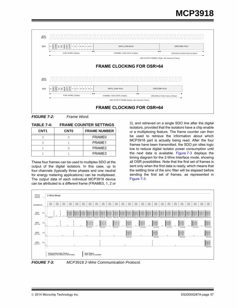
MCP3918
FIGURE 7-2: Frame Word.
These four frames can be used to multiplex SDO at theoutput of the digital isolators. In this case, up tofour channels (typically three phases and one neutralfor energy metering applications) can be multiplexed.The output data of each individual MCP3918 devicecan be attributed to a different frame (FRAME0, 1, 2 or
3), and retrieved on a single SDO line after the digitalisolators, provided that the isolators have a chip enableor a multiplexing feature. The frame counter can thenbe used to retrieve the information about whichMCP3918 part is actually being read. After the fourframes have been transmitted, the SDO pin idles logiclow to reduce digital isolator power consumption untilthe next data is available. Figure 7-3 displays thetiming diagram for the 2-Wire Interface mode, showingall OSR possibilities. Note that the first set of frames issent only when the first data is ready, which means thatthe settling time of the sinc filter will be elapsed beforesending the first set of frames, as represented inFigure 7-3.
FIGURE 7-3: MCP3918 2-Wire Communication Protocol.
CRCCOM<15:0>
0 DATA_CH0<23:0>
SYNC WORD (2 Bytes)
SDO OUTPUT FRAME (7 Bytes, 56x clocks per Frame)O
SR
0O
SR
1
G1
G0
BO
OST
CN
T1C
NT0 01 1 0 10 0 1
CHANNEL 0 ADC DATA (3 Bytes)
SDO
SCK/MCLK
CRCCOM<15:0>
CRCCOM on Entire Frame (2 Bytes)
DATA_CH0<15:0>0
SYNC WORD (2 Bytes)
SDO OUTPUT FRAME (6 Bytes, 48x clocks per Frame)
OS
R0
OS
R1
G1
G0
BOO
ST
CN
T1C
NT0 01 1 0 10 0 1
CHANNEL 0 ADC DATA (2 Bytes)
SDO
SCK/MCLK
FRAME CLOCKING FOR OSR>64
FRAME CLOCKING FOR OSR=64
CRCCOM on Entire Frame (2 Bytes)
TABLE 7-4: FRAME COUNTER SETTINGS
CNT1 CNT0 FRAME NUMBER
0 0 FRAME0
0 1 FRAME1
1 0 FRAME2
1 1 FRAME3
SDO(OSR=64)
0 0
Internal data ready (Data is unsettled). No frame is transmitted
Data Ready.New data is available
OSC2/MODE
256x clocks
256x clocks
256x clocksSCK/MCLK
256x clocks
256x clocks
256x clocks
256x clocks
256x clocks
256x clocks
256x clocks
256x clocks
256x clocks
256x clocks
256x clocks
256x clocks
256x clocks
256x clocks
256x clocks
256x clocks
256x clocks
256x clocks
256x clocks
256x clocks
256x clocks
256x clocks
DATA=D1 DATA=D2 DATA=D3 DATA=D4DATA=0 DATA=D5 DATA=D6 DATA=D7 DATA=D8 DATA=D9 DATA=D10 DATA=D11 DATA=D12 DATA=D13 DATA=D14 DATA=D15 DATA=D16 DATA=D17 DATA=D18 DATA=D19 DATA=D20 DATA=D21 DATA=D22
FRAME0
FRAME1
FRAME2
FRAME3
FRAME0
FRAME1
FRAME2
FRAME3
FRAME0
FRAME1
FRAME2
FRAME3
0DATA=D1 DATA=D2 DATA=D3 DATA=D4 DATA=D5 DATA=D6 DATA=D7 DATA=D8 DATA=D9 DATA=D10
0DATA=D1 DATA=D2 DATA=D3 DATA=D4
0DATA=D1
0 0
0
0 0
0 0 0 0
0 0 0 0 0 0 0 0 0
2-Wire Mode
Hi-Z
Hi-Z
Hi-Z
Hi-Z
SDO(OSR=128)
SDO(OSR=256)
SDO(OSR=512)
0
0
0
0
FRAME0
FRAME1
FRAME2
FRAME3
FRAME0
FRAME1
FRAME2
FRAME3
FRAME0
FRAME1
FRAME2
FRAME3
FRAME0
FRAME1
FRAME2
FRAME3
FRAME0
FRAME1
FRAME2
FRAME3
FRAME0
FRAME1
FRAME2
FRAME3
FRAME0
FRAME1
FRAME2
FRAME3
FRAME0
FRAME1
FRAME2
FRAME3
FRAME0
FRAME1
FRAME2
FRAME3
FRAME0
FRAME1
FRAME2
FRAME3
FRAME0
FRAME1
FRAME2
FRAME3
FRAME0
FRAME1
FRAME2
FRAME3
FRAME0
FRAME1
FRAME2
FRAME3
FRAME0
FRAME1
FRAME2
FRAME3
FRAME0
FRAME1
FRAME2
FRAME3
FRAME0
FRAME1
FRAME2
FRAME3
FRAME0
FRAME1
FRAME2
FRAME3
FRAME0
FRAME1
FRAME2
FRAME3
FRAME0
FRAME1
FRAME2
FRAME3
FRAME0
FRAME1
FRAME2
FRAME3
FRAME0
FRAME1
FRAME2
FRAME3
FRAME0
FRAME1
FRAME2
FRAME3
FRAME0
FRAME1
FRAME2
FRAME3
FRAM
E0FRAM
E1FRAM
E2FRAM
E3
FRAM
E0FRAM
E1FRAM
E2FRAM
E3
FRAME0
FRAME1
FRAME2
FRAME3
FRAME0
FRAME1
FRAME2
FRAME3
FRAME0
FRAME1
FRAME2
FRAME3
FRAME0
FRAME1
FRAME2
FRAME3
FRAME0
FRAME1
FRAME2
FRAME3
FRAM
E0FRAM
E1FRAM
E2FRAM
E3
FRAM
E0FRAM
E1FRAM
E2FRAM
E3
FRAME0
FRAME1
FRAME2
FRAME3
FRAME0
FRAME1
FRAME2
FRAME3
2014 Microchip Technology Inc. DS20005287A-page 57
MCP3918
7.4 Watchdog Timer Reset, Resetting the Part when in 2-Wire Mode
When the part has entered 2-Wire mode, the HardReset mode functionality is not available because theRESET pin becomes the logic input for OSR0. If theuser wants to execute a full reset of the part withoutdoing a POR, the 2-Wire mode incorporates an internalwatchdog timer that automatically performs a full resetof the part, provided that the timer has elapsed.
The watchdog timer starts synchronously with eachrising edge of SCK/MCLK. If the SCK logic high state ismaintained for a time that is larger than tWATCH, thewatchdog timer circuit forces the full reset of the chip,which then returns to its default configuration with theADC being reset. If the SCK logic high state ismaintained for a time shorter than tWATCH and thenSCK/MCLK toggles to logic low, the internal timer iscleared, waiting for another rising edge to restart.
The watchdog timer functionality induces a restrictionin the usable range of frequencies on SCK/MCLK. Inorder to avoid intermittent resets in all cases, theminimum SCK/MCLK frequency in 2-Wire Interfacemode is equal to the inverse of the minimum tWATCHtime (1/(2 x 3.6 µs) = 138.9 kHz, if the duty cycle of theSCK/MCLK is 50%).
The watchdog timer starts only on the rising edge ofSCK/MCLK, not on the falling edge. MaintainingSCK/MCLK at a logic low state for large periods of timedoes not create any watchdog timer resets. AWatchdog Timer Reset is created only when theSCK/MCLK state is maintained logic high during a longenough period of time.
This watchdog timer period permits exiting the 2-Wireinterface, if desired, by toggling the OSC2/MODE pin tologic low before creating the Watchdog Timer Resetand maintaining it logic low until the reset occurs.
DS20005287A-page 58 2014 Microchip Technology Inc.
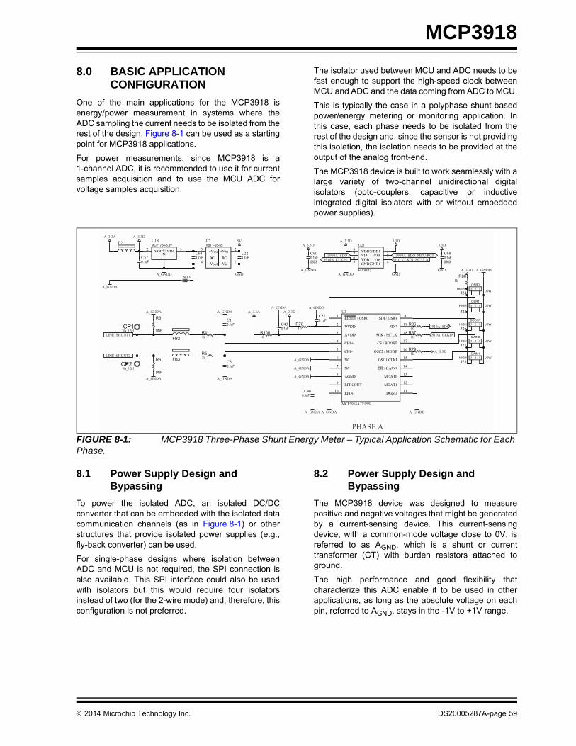
MCP3918
8.0 BASIC APPLICATION CONFIGURATION
One of the main applications for the MCP3918 isenergy/power measurement in systems where theADC sampling the current needs to be isolated from therest of the design. Figure 8-1 can be used as a startingpoint for MCP3918 applications.
For power measurements, since MCP3918 is a1-channel ADC, it is recommended to use it for currentsamples acquisition and to use the MCU ADC forvoltage samples acquisition.
The isolator used between MCU and ADC needs to befast enough to support the high-speed clock betweenMCU and ADC and the data coming from ADC to MCU.
This is typically the case in a polyphase shunt-basedpower/energy metering or monitoring application. Inthis case, each phase needs to be isolated from therest of the design and, since the sensor is not providingthis isolation, the isolation needs to be provided at theoutput of the analog front-end.
The MCP3918 device is built to work seamlessly with alarge variety of two-channel unidirectional digitalisolators (opto-couplers, capacitive or inductiveintegrated digital isolators with or without embeddedpower supplies).
FIGURE 8-1: MCP3918 Three-Phase Shunt Energy Meter – Typical Application Schematic for Each Phase.
8.1 Power Supply Design and Bypassing
To power the isolated ADC, an isolated DC/DCconverter that can be embedded with the isolated datacommunication channels (as in Figure 8-1) or otherstructures that provide isolated power supplies (e.g.,fly-back converter) can be used.
For single-phase designs where isolation betweenADC and MCU is not required, the SPI connection isalso available. This SPI interface could also be usedwith isolators but this would require four isolatorsinstead of two (for the 2-wire mode) and, therefore, thisconfiguration is not preferred.
8.2 Power Supply Design and Bypassing
The MCP3918 device was designed to measurepositive and negative voltages that might be generatedby a current-sensing device. This current-sensingdevice, with a common-mode voltage close to 0V, isreferred to as AGND, which is a shunt or currenttransformer (CT) with burden resistors attached toground.
The high performance and good flexibility thatcharacterize this ADC enable it to be used in otherapplications, as long as the absolute voltage on eachpin, referred to AGND, stays in the -1V to +1V range.
3910A_SDO
A_GNDD
A_GNDA
A_GNDA
10R76
0.1uFC52
10R100
0.1uFC43
10R86
A_GNDA
A_GNDA
A_GNDA
0.1uFC46
A_3.3DA_3.3AA_GNDD
DR / GAIN1 14
DGND 11
AGND8
CH0-5
DVDD2
OSC1/CLKI 15
SCK / MCLK 18
MDAT1 12
MDAT0 13
NC6
NC7
RFIN/OUT+9
RFIN-10
RESET / OSR01
AVDD3
CH0+4 CS / BOOST 17
OSC2 / MODE 16
SDO 19
SDI / OSR1 20
DR / GAIN1
DGND
AGND
CH0-
DVDD
OSC1/CLKI
SCK / MCLK
MDAT1
MDAT0
NC
NC
RFIN/OUT+
RFIN-
RESET / OSR0
AVDD
CH0+ CS / BOOST
OSC2 / MODE
SDO
SDI / OSR1
U3
MCP3918A1T/ISS
123J24
123
J25
A_3.3D
1kR80
A_GNDD
123J26
123J27
123J28
HIGH LOW
HIGH LOW
LOW
LOW
HIGH
HIGHGAIN1
GAIN0
BOOST
OSR1
OSR0HIGH
LOW
1kR79
3910A_CLKIN10R87
3910A_SDO
A_GNDD
A_3.3D
3910A_CLKIN 3910_CLKIN_MCU_A
PHASE A
A_3.3D
A_3.3D
A_3.3A
A_GNDA
VBT1-S5-S5
-Vin 1
+Vin 2+Vout5
-Vout4 -Vin
+Vin+Vout
-Vout
DCDC
U7
4.7uFC63
MCP1754-3.3VVIN 3
GND
1
VOUT2 VIN
GNDVOUT ND
ND
U18
A_GNDD
0.1uFC57 4.7uF
C22
5VL2
GND
3.3D
GND
0.1uF0603
C68
3.3D
GND
0.1uF0603
C60
A_3.3D
A_GNDD
NT3
3910A_SDO_MCU/RC3VDD1 1
VOA 2
VIB 3
GND1 4
VDD28
VIA7
VOB6
GND25
VDD1VOAVIB
GND1
VDD2VVVIAVOBGND2GG
FOD8012
U21
A_GNDA
A_GNDA
A_GNDAA_GNDA
A_GNDA
0.1uFC5
1kR5
1kR4
0.1uFC1
LINE_SHUNT1
LINE_SHUNT2
Via_1.6x1CP1
Via_1.6x1CP2
DNP
R3
DNP
R6
FB2
FB3
2014 Microchip Technology Inc. DS20005287A-page 59

MCP3918
In any system, the analog ICs (such as references oroperational amplifiers) are always connected to theanalog ground plane. The MCP3918 should also beconsidered as a sensitive analog component, andshould be connected to the analog ground plane. TheADC features two pairs of pins: AGND, AVDD, DGND andDVDD. For best performance, it is recommended tokeep the two pairs connected to two different networks(Figure 8-2). This way, the design will feature twoground traces and two power supplies (Figure 8-3).This means the analog circuitry (including MCP3918)and the digital circuitry (MCU) should have separatepower supplies and return paths to the external groundreference, as described in Figure 8-2.
An example of a typical power supply circuit, withdifferent lines for analog and digital power, is shown inFigure 8-3. A possible split example is shown inFigure 8-4, where the ground star connection can bedone at the bottom of the device with the exposed pad.The split between analog and digital can be done underthe device, and AVDD and DVDD can be connectedtogether with lines coming under the ground plane.Another possibility, sometimes easier to implement interms of PCB layout, is to consider the MCP3918 as ananalog component and, therefore, to connect bothAVDD and DVDD together, and AGND and DGNDtogether, with a star connection. In this scheme, thedecoupling capacitors may be larger, due to the rippleon the digital power supply (caused by the digital filtersand the SPI interface of the MCP3918) now causingglitches on the analog power supply.
FIGURE 8-2: All Analog and Digital Return Paths Need to Stay Separate with Proper Bypass Capacitors.
FIGURE 8-3: Power Supply with Separate Lines for Analog and Digital Sections.
VA VD
MCU
“Star” Point
IA
ID
IDIA
AVDD DVDD
AGND DGND
D-= A-=
0.1 μF
MCP39XX
0.1 μF C
Note: The “Net Tie” Object NT2 represents the start ground connection.
DS20005287A-page 60 2014 Microchip Technology Inc.

MCP3918
FIGURE 8-4: Separation of Analog and Digital Circuits on Layout.
Figure 7-5 shows a more detailed example with a directconnection to a high-voltage line (e.g., a two-wire 120Vor 220V system). A current-sensing shunt is used forcurrent measurement on the high/line side that alsosupplies the ground for the system. This is necessaryas the shunt is directly connected to the channel inputpins of the MCP3918. To reduce sensitivity to externalinfluences, such as EMI, these two wires should form atwisted pair, as noted in Figure 8-5. The power supplyand MCU are separated on the right side of the PCB,surrounded by the digital ground plane. The MCP3918is kept on the left side, surrounded by the analogground plane. There are two separate power suppliesgoing to the digital section of the system and the analogsection, including the MCP3918. With this placement,there are two separate current supply paths andcurrent return paths, IA and ID.
FIGURE 8-5: Connection Diagram.
The ferrite bead between the digital and analog groundplanes helps keep high-frequency noise from enteringthe device. This ferrite bead is recommended to be lowresistance; most often it is a THT component. Ferritebeads are typically placed on the shunt inputs and intothe power supply circuit for additional protection.
8.3 SPI Interface Digital Crosstalk
The MCP3918 incorporates a high-speed 20-MHz SPIdigital interface. This interface can induce a crosstalk,if it is running at its full speed without any precautions.The crosstalk is caused by the switching noise createdby the digital SPI signals (also called ground bouncing).
This crosstalk would negatively impact the SNR in thiscase. The noise is attenuated if a proper separationbetween the analog and digital power supplies is put inplace (see Section 8.2 “Power Supply Design andBypassing”). In order to further remove the influenceof the SPI communication on measurement accuracy,it is recommended to add series resistors on the SPIlines to reduce the current spikes caused by the digitalswitching noise (see Figure 8-1 where these resistorshave been implemented). The resistors also help tokeep the level of electromagnetic emissions low. Themeasurement graphs provided in this data sheet havebeen performed with 100series resistors connectedon each SPI I/O pin. Measurement accuracy distur-bances have not been observed even at the full speedof 20 MHz interfacing. The crosstalk performance isdependent on the package choice due to the differencein the pin arrangement (dual in-line or quad), and isimproved in the QFN-20 package.
MCU
Power SupplyCircuitry
LINE
NEUTRAL
SHUNT
Twisted Pair
IA
ID
ID
IA
“Star” Point
VAVD
Analog Ground Plane Digital Ground Plane
MCP3918
2014 Microchip Technology Inc. DS20005287A-page 61

MCP3918
8.4 Sampling Speed and Bandwidth
If ADC power consumption is not a concern in thedesign, the boost settings can be increased for bestperformance so that the OSR is always kept at themaximum settings to improve the SINAD performance(see Table 7-1). If the MCU cannot generate a clockfast enough, it is possible to tap the OSC1/OSC2 pinsof the MCP3918 crystal oscillator directly to the crystalof the microcontroller. When the sampling frequency isenlarged, the phase resolution is improved, and withthe OSR increased, the phase compensation rangecan be kept in the same range as the default settings.
8.5 Differential Inputs Anti-Aliasing Filter
Due to the nature of the ADC used in the MCP3918(oversampling converter), each differential input of theADC channels requires an anti-aliasing filter so that theoversampling frequency (DMCLK) is largely attenuatedand does not generate any disturbances on the ADCaccuracy. This anti-aliasing filter also needs to have again close to the one in the signal bandwidth of interest.Typically, for 50/60 Hz measurement and defaultsettings (DMCLK = 1 MHz), a simple RC filter with1 k and 100 nF can be used. The anti-aliasing filterused for the measurement graphs is a first-order RCfilter with 1 kand 15 nF. The typical schematic forconnecting a current transformer to the ADC is shownin Figure 8-6. If wires are involved, twisting them is alsorecommended.
FIGURE 8-6: First-Order Anti-Aliasing Filter for CT-Based Designs.
The di/dt current sensors, such as Rogowski coils, canbe an alternative to current transformers. Since thesesensing elements are highly sensitive tohigh-frequency electromagnetic fields, using asecond-order anti-aliasing filter is recommended toincrease the attenuation of potential perturbing RFsignals.
FIGURE 8-7: Second-Order Anti-Aliasing Filter for Rogowski Coil-Based Designs.
The filter presented in Figure 8-7 is an anti-aliasingfilter. The di/dt integrator can be created in firmware asa first-order low-pass filter with corner frequency muchlower than the input signal.
The MCP3918 is highly recommended in applicationsusing di/dt as current sensors because of the extremelylow noise floor at low frequencies. In such applications,a low-pass filter (LPF) with a cut-off frequency muchlower than the signal frequency (50/60 Hz for metering)is used to compensate for the 90 degree shift and forthe 20 db/decade attenuation induced by the di/dtsensor. Because of this filter, the SNR will bedecreased, since the signal will be attenuated by a feworders of magnitude, while the low-frequency noise willnot be attenuated. Usually, a high-order high-pass filter(HPF) is used to attenuate the low-frequency noise inorder to prevent a dramatic degradation of the SNR,which can be very important in other parts. A high-orderfilter will also consume a significant portion of thecomputation power of the MCU. When using theMCP3918, such a high-order HPF is not required, sincethis part has a low noise floor at low frequencies. Afirst-order HPF is enough to achieve very goodaccuracy.
TABLE 8-1: SAMPLING SPEED VS. MCLK AND OSR, ADC PRESCALE 1:1
MCLK(MHz)
Boost OSRSampling
Speed (ksps)
16 0b11 1024 3.91
14 0b11 1024 3.42
12 0b11 1024 2.93
10 0b10 1024 2.44
8 0b10 512 3.91
6 0b01 512 2.93
4 0b01 256 3.91
DS20005287A-page 62 2014 Microchip Technology Inc.
MCP3918
8.6 Energy Measurement Error Considerations
The measurement error is a typical representation ofthe non-linearity of the ADC (see Section 4.0“Terminology and Formulas” for the definition ofmeasurement error). The measurement error isdependent on the THD and on the noise floor of theADC. The measurement error specification on theMCP3918 can be improved by increasing the OSR (toget a better SINAD and THD performance) and, tosome extent, the BOOST settings (if the bandwidth ofthe measurements is too limited by the bandwidth ofthe amplifiers in the sigma-delta ADC). In most of theenergy metering AC applications, high-pass filters areused to cancel the offset on each ADC channel (currentand voltage channels), and therefore a single-pointcalibration is necessary to calibrate the system foractive energy measurement. This calibration is asystem gain calibration, and the user can utilize theEN_GAINCAL bit and the GAINCAL_CH0 register toperform this digital calibration. After such calibration,typical measurement error curves like the ones inFigure 2-7 can be generated by sweeping the currentchannel amplitude and measuring the energy at theoutputs (the energy calculations here are beingrealized off-chip). The error is measured using a gain of1x, as it is commonly used in most CT-basedapplications.
At low signal amplitude values (typically 1000:1dynamic range and higher), the crosstalk betweenchannels, mainly caused by the PCB, becomes asignificant part of the perturbation as the measurementerror increases. The 1-point measurement error curvesin Figure 2-5 have been performed with a full-scalesine wave on all the inputs that are not measured,which means that these channels induce a maximumamount of crosstalk on the measurement error curve.In order to avoid such behavior, a 2-point calibrationcan be put in place in the calculation section.
This 2-point calibration can be a simple linearinterpolation between two calibration points (one athigh amplitudes, one at low amplitudes at each end ofthe dynamic range) and helps to significantly lower theeffect of crosstalk between channels. A 2-pointcalibration is very effective in maintaining themeasurement error close to zero on the whole dynamicrange, since the non-linearity and distortion of theMCP3918 is very low. Figure 2-6 shows themeasurement error curves obtained with the sameADC data taken for Figure 2-5, but where a 2-pointcalibration has been applied. The difference issignificant only at the low end of the dynamic range,where all the perturbing factors are a bigger part of theADC output signals. These curves show extremely tightmeasurement error across the full dynamic range(here, typically 10,000:1), which is required inhigh-accuracy class meters.
2014 Microchip Technology Inc. DS20005287A-page 63

MCP3918
NOTES:
DS20005287A-page 64 2014 Microchip Technology Inc.

MCP3918
9.0 MCP3918 INTERNAL REGISTERS
The addresses associated with the internal registersare listed in Table 9-1. This section also describes theregisters in detail. All registers are 24-bit long registers,which can be addressed and read separately.
The format of the data register (0x00) can be changedthrough the WIDTH_CRC and WIDTH_DATA<1:0> bitsin the STATUSCOM register. The READ<1:0> andWRITE bits define the groups and types of registers forcontinuous read/write communication or looping onaddress sets, as shown in Table 9-2.
TABLE 9-1: MCP3918 REGISTER MAP
Address Name Bits R/W Description
0x00 CHANNEL0 24 R Channel 0 ADC Data <23:0>, MSB first
0x01 Unused 24 U Unused
0x02 Unused 24 U Unused
0x03 Unused 24 U Unused
0x04 Unused 24 U Unused
0x05 Unused 24 U Unused
0x06 Unused 24 U Unused
0x07 Unused 24 U Unused
0x08 MOD 24 R/W Delta-sigma Modulators Output Value
0x09 PHASE 24 U Phase Delay Configuration Register
0x0A Unused 24 U Unused
0x0B GAIN 24 R/W Gain Configuration Register
0x0C STATUSCOM 24 R/W Status and Communication Register
0x0D CONFIG0 24 R/W Configuration Register
0x0E CONFIG1 24 R/W Configuration Register
0x0F OFFCAL_CH0 24 R/W Offset Correction Register - Channel 0
0x10 GAINCAL_CH0 24 R/W Gain Correction Register - Channel 0
0x11 Unused 24 U Unused
0x12 Unused 24 U Unused
0x13 Unused 24 U Unused
0x14 Unused 24 U Unused
0x15 Unused 24 U Unused
0x16 Unused 24 U Unused
0x17 Unused 24 U Unused
0x18 Unused 24 U Unused
0x19 Unused 24 U Unused
0x1A Unused 24 U Unused
0x1B Unused 24 U Unused
0x1C Unused 24 U Unused
0x1D Unused 24 U Unused
0x1E Unused 24 U Unused
0x1F LOCK/CRC 24 R/W Security Register (password and CRC-16 on Register Map)
2014 Microchip Technology Inc. DS20005287A-page 65
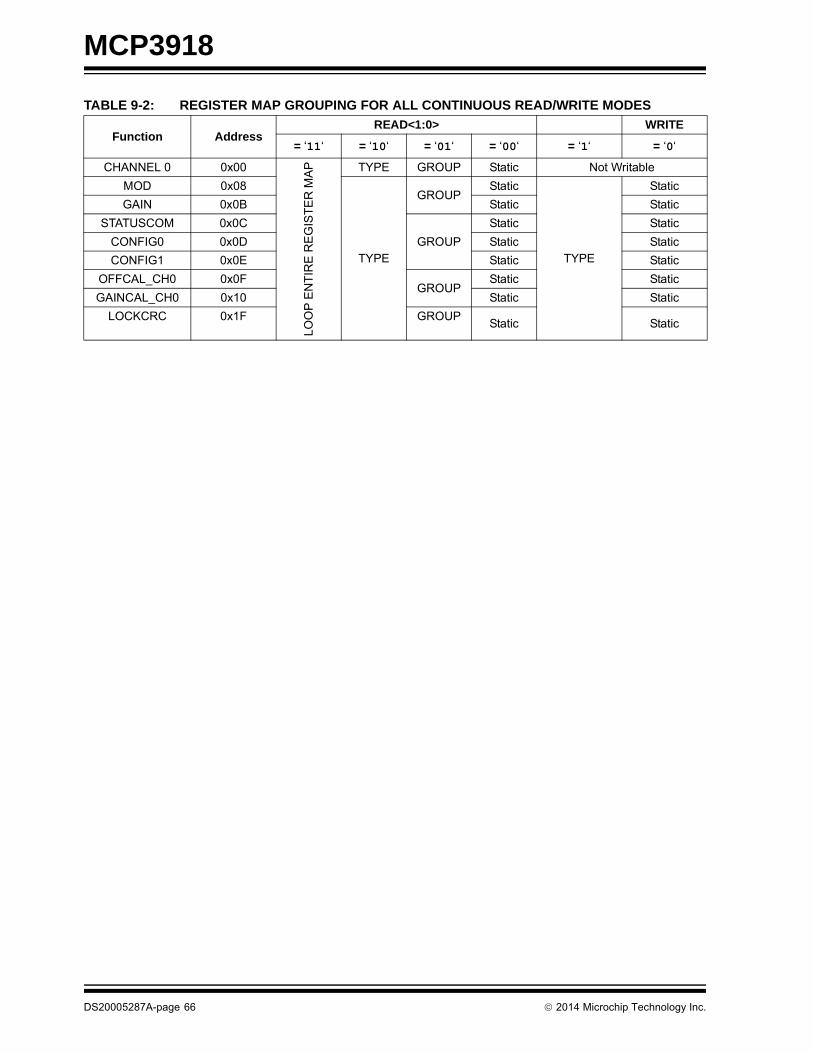
MCP3918
TABLE 9-2: REGISTER MAP GROUPING FOR ALL CONTINUOUS READ/WRITE MODES
Function AddressREAD<1:0> WRITE
= ‘11‘ = ‘10‘ = ‘01‘ = ‘00‘ = ‘1‘ = ‘0‘
CHANNEL 0 0x00
LOO
P E
NT
IRE
RE
GIS
TE
R M
AP TYPE GROUP Static Not Writable
MOD 0x08
TYPE
GROUPStatic
TYPE
Static
GAIN 0x0B Static Static
STATUSCOM 0x0C
GROUP
Static Static
CONFIG0 0x0D Static Static
CONFIG1 0x0E Static Static
OFFCAL_CH0 0x0FGROUP
Static Static
GAINCAL_CH0 0x10 Static Static
LOCKCRC 0x1F GROUPStatic Static
DS20005287A-page 66 2014 Microchip Technology Inc.

MCP3918
9.1 CHANNEL Register – ADC Channel Data Output Register
The ADC Channel Data Output register alwayscontains the most recent A/D conversion data. Thisregister is read-only. This register is latched when anADC read communication occurs. When a data readyevent occurs during a read communication, the mostcurrent ADC data is also latched to avoid datacorruption issues. The three bytes of each channel areupdated synchronously at a DRCLK rate. They can beaccessed separately, if needed, but are refreshedsynchronously.
Name Bits Address Cof.
CHANNEL0 24 0x00 R
REGISTER 9-1: CHANNEL REGISTER
R-0 R-0 R-0 R-0 R-0 R-0 R-0 R-0
DATA_CH0<23> (MSB)
DATA_CH0<22>
DATA_CH0<21>
DATA_CH0<20>
DATA_CH0<19>
DATA_CH0<18>
DATA_CH0<17>
DATA_CH0<16>
bit 23 bit 16
R-0 R-0 R-0 R-0 R-0 R-0 R-0 R-0
DATA_CH0<15>
DATA_CH0<14>
DATA_CH0<13>
DATA_CH0<12>
DATA_CH0<11>
DATA_CH0<10>
DATA_CH0<9>
DATA_CH0<8>
bit 15 bit 8
R-0 R-0 R-0 R-0 R-0 R-0 R-0 R-0
DATA_CH0<7>
DATA_CH0<6>
DATA_CH0<5>
DATA_CH0<4>
DATA_CH0<3>
DATA_CH0<2>
DATA_CH0<1>
DATA_CH0<0>
bit 7 bit 0
Legend:
R = Readable bit W = Writable bit U = Unimplemented bit, read as ‘0’
-n = Value at POR ‘1’ = Bit is set ‘0’ = Bit is cleared x = Bit is unknown
bit 23-0 DATA_CH0: Output code from ADC. This data is post-calibration if the EN_OFFCAL or EN_GAINCALbits are enabled. This data can be formatted in 16-/24-/32-bit modes, depending on the WIDTH_-DATA<1:0> settings. (See Section 5.5 “ADC Output Coding”.)
2014 Microchip Technology Inc. DS20005287A-page 67
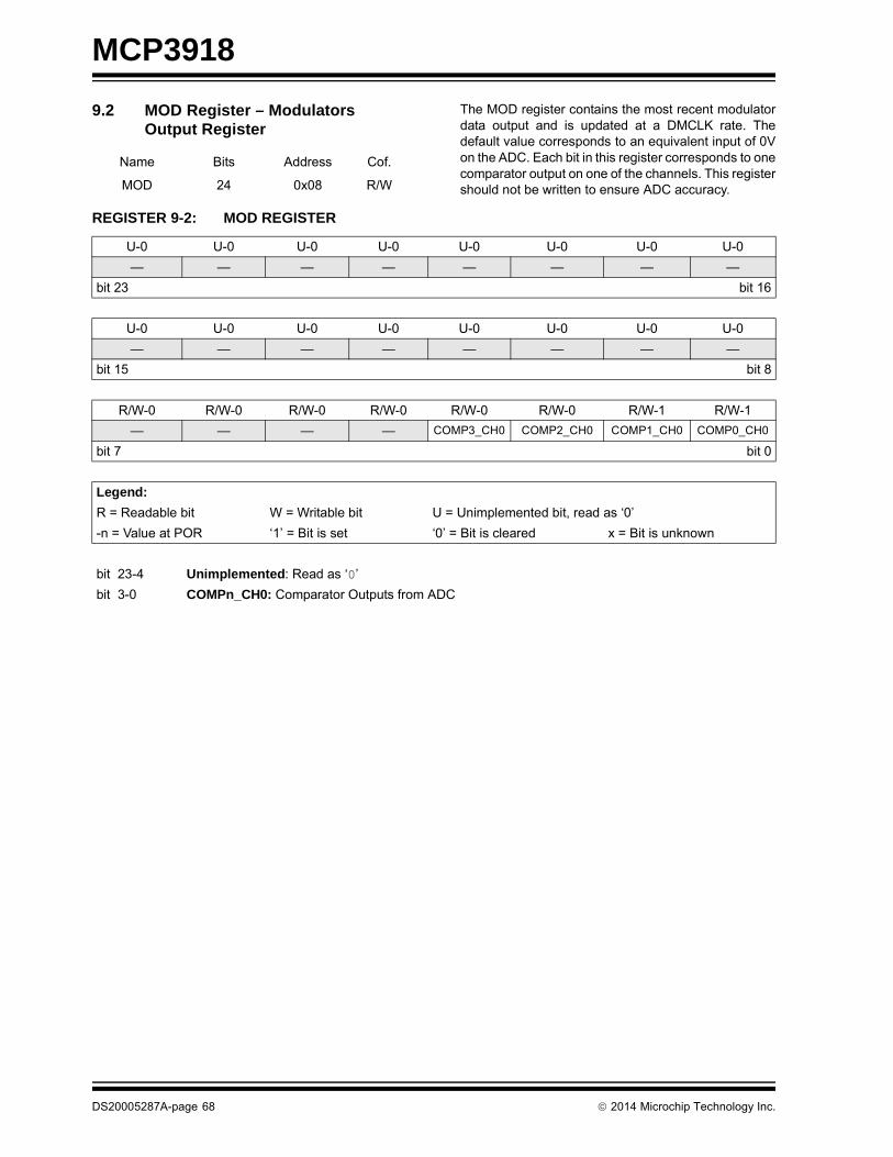
MCP3918
9.2 MOD Register – Modulators Output Register
The MOD register contains the most recent modulatordata output and is updated at a DMCLK rate. Thedefault value corresponds to an equivalent input of 0Von the ADC. Each bit in this register corresponds to onecomparator output on one of the channels. This registershould not be written to ensure ADC accuracy.
Name Bits Address Cof.
MOD 24 0x08 R/W
REGISTER 9-2: MOD REGISTER
U-0 U-0 U-0 U-0 U-0 U-0 U-0 U-0
— — — — — — — —
bit 23 bit 16
U-0 U-0 U-0 U-0 U-0 U-0 U-0 U-0
— — — — — — — —
bit 15 bit 8
R/W-0 R/W-0 R/W-0 R/W-0 R/W-0 R/W-0 R/W-1 R/W-1
— — — — COMP3_CH0 COMP2_CH0 COMP1_CH0 COMP0_CH0
bit 7 bit 0
Legend:
R = Readable bit W = Writable bit U = Unimplemented bit, read as ‘0’
-n = Value at POR ‘1’ = Bit is set ‘0’ = Bit is cleared x = Bit is unknown
bit 23-4 Unimplemented: Read as ‘0’
bit 3-0 COMPn_CH0: Comparator Outputs from ADC
DS20005287A-page 68 2014 Microchip Technology Inc.

MCP3918
9.3 PHASE Register – Phase Configuration Register
Any write to this register automatically resets andrestarts the active ADC.
Name Bits Address Cof.
PHASE 24 0x0A R/W
REGISTER 9-3: PHASE REGISTER
U-0 U-0 U-0 U-0 U-0 U-0 U-0 U-0
— — — — — — — —
bit 23 bit 16
U-0 U-0 U-0 U-0 R/W-0 R/W-0 R/W-0 R/W-0
— — — — PHASE<11> PHASE<10> PHASE<9> PHASE<8>
bit 15 bit 8
R/W-0 R/W-0 R/W-0 R/W-0 R/W-0 R/W-0 R/W-0 R/W-0
PHASE<7> PHASE<6> PHASE<5> PHASE<4> PHASE<3> PHASE<2> PHASE<1> PHASE<0>
bit 7 bit 0
Legend:
R = Readable bit W = Writable bit U = Unimplemented bit, read as ‘0’
-n = Value at POR ‘1’ = Bit is set ‘0’ = Bit is cleared x = Bit is unknown
bit 23-12 Unimplemented: Read as ‘0’
bit 11-0 PHASE<11:0> Conversion Start delay. Delay = (PHASE<11:0> decimal code + OSR/2)/DMCLK.
2014 Microchip Technology Inc. DS20005287A-page 69
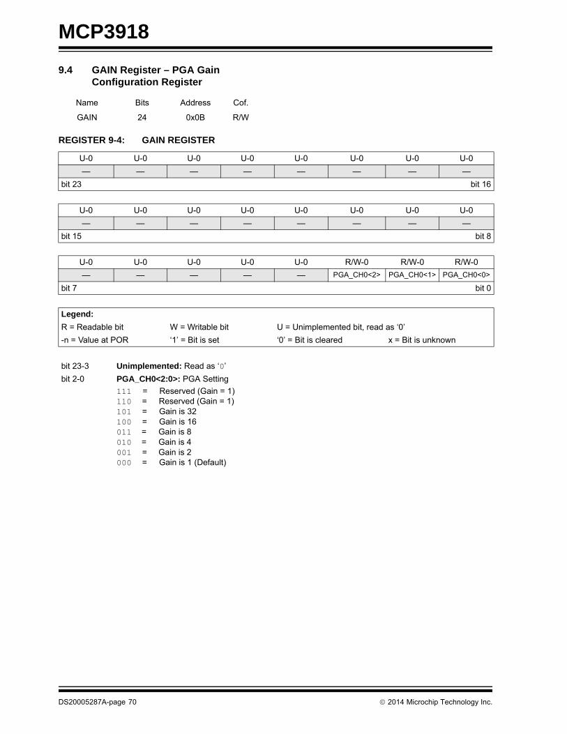
MCP3918
9.4 GAIN Register – PGA Gain Configuration Register
Name Bits Address Cof.
GAIN 24 0x0B R/W
REGISTER 9-4: GAIN REGISTER
U-0 U-0 U-0 U-0 U-0 U-0 U-0 U-0
— — — — — — — —
bit 23 bit 16
U-0 U-0 U-0 U-0 U-0 U-0 U-0 U-0
— — — — — — — —
bit 15 bit 8
U-0 U-0 U-0 U-0 U-0 R/W-0 R/W-0 R/W-0
— — — — — PGA_CH0<2> PGA_CH0<1> PGA_CH0<0>
bit 7 bit 0
Legend:
R = Readable bit W = Writable bit U = Unimplemented bit, read as ‘0’
-n = Value at POR ‘1’ = Bit is set ‘0’ = Bit is cleared x = Bit is unknown
bit 23-3 Unimplemented: Read as ‘0’
bit 2-0 PGA_CH0<2:0>: PGA Setting
111 = Reserved (Gain = 1)110 = Reserved (Gain = 1)101 = Gain is 32100 = Gain is 16011 = Gain is 8010 = Gain is 4001 = Gain is 2000 = Gain is 1 (Default)
DS20005287A-page 70 2014 Microchip Technology Inc.
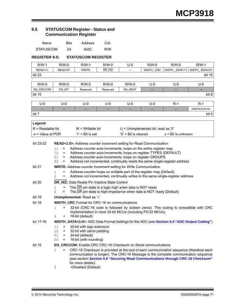
MCP3918
9.5 STATUSCOM Register - Status and Communication Register
Name Bits Address Cof.
STATUSCOM 24 0x0C R/W
REGISTER 9-5: STATUSCOM REGISTER
R/W-1 R/W-0 R/W-1 R/W-0 U-0 R/W-0 R/W-0 R/W-1
READ<1> READ<0> WRITE DR_HIZ — WIDTH_ CRC WIDTH_ DATA<1> WIDTH_ DATA<0>
bit 23 bit 16
R/W-0 R/W-0 R/W-0 R/W-0 R/W-0 U-0 U-0 U-0
EN_CRCCOM EN_INT Reserved Reserved EN_MDAT — — —
bit 15 bit 8
U-0 U-0 U-0 U-0 U-0 U-0 R-1 R-1
— — — — — — — DRSTATUS<0>
bit 7 bit 0
Legend:
R = Readable bit W = Writable bit U = Unimplemented bit, read as ‘0’
-n = Value at POR ‘1’ = Bit is set ‘0’ = Bit is cleared x = Bit is unknown
bit 23-22 READ<1:0>: Address counter increment setting for Read Communication
11 = Address counter auto-increments, loops on the entire register map10 = Address counter auto-increments, loops on register TYPES (DEFAULT)01 = Address counter auto-increments, loops on register GROUPS00 = Address not incremented, continually reads the same single-register address
bit 21 WRITE: Address counter increment setting for Write Communication
1 = Address counter loops on writable part of the register map (Default)0 = Address not incremented, continually writes to the same single-register address
bit 20 DR_HIZ: Data Ready Pin Inactive State Control
1 = The DR pin state is a logic high when data is NOT ready0 = The DR pin state is high-impedance when data is NOT ready (Default)
bit 19 Unimplemented: Read as ‘0’
bit 18 WIDTH_CRC Format for CRC-16 on communications
1 = 32-bit (CRC-16 code is followed by sixteen zeros). This coding is compatible with CRCimplementation in most 32-bit MCUs (including PIC32 MCUs).
0 = 16-bit (default)
bit 17-16 WIDTH_DATA<1:0>: ADC Data Format Settings for the ADC (see Section 5.5 “ADC Output Coding”)
11 = 32-bit with sign extension10 = 32-bit with zeros padding01 = 24-bit (default)00 = 16-bit (with rounding)
bit 15 EN_CRCCOM: Enable CRC CRC-16 Checksum on Serial communications
1 = CRC-16 Checksum is provided at the end of each communication sequence (therefore eachcommunication is longer). The CRC-16 Message is the complete communication sequence(see section Section 6.9 “Securing Read Communications through CRC-16 Checksum”for more details).
0 =Disabled (Default)
2014 Microchip Technology Inc. DS20005287A-page 71

MCP3918
bit 14 EN_INT: Enable the CRCREG interrupt function
1 = The interrupt flag for the CRCREG checksum verification is enabled. The Data Ready pin(DR) will become logic low and stays logic low if a CRCREG checksum error happens. Thisinterrupt is cleared if the LOCK<7:0> value is made equal to the PASSWORD value (0xA5).
0 = The interrupt flag for the CRCREG checksum verification is disabled. The CRCREG<15:0>bits are still calculated properly and can still be read in this mode.
bit 13-12 Reserved: These bits should be kept equal to '0' at all times.
bit 11 EN_MDAT: Enable Modulator Output
1 = MDAT0 output is enabled0 = MDAT0 output is disabled (DEFAULT)
bit 10-1 Unimplemented: Read as ‘0’
bit 0 DRSTATUS: Data Ready status bit
DRSTATUS = 1 - Channel CH0 data is not ready (DEFAULT)DRSTATUS = 0 - Channel CH0 data is ready. The status bit is set back to '1' after reading the
STATUSCOM register. The status bit is not set back to '1' by the read of thecorresponding channel ADC data.
REGISTER 9-5: STATUSCOM REGISTER (CONTINUED)
DS20005287A-page 72 2014 Microchip Technology Inc.
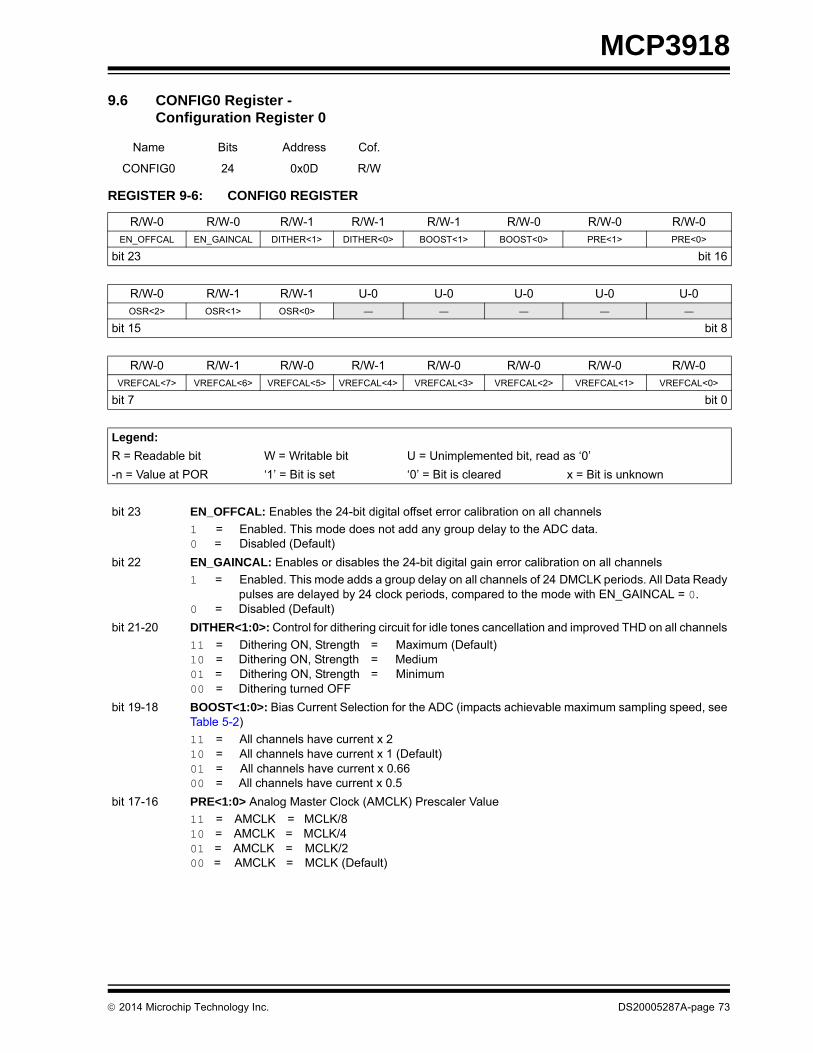
MCP3918
9.6 CONFIG0 Register - Configuration Register 0
Name Bits Address Cof.
CONFIG0 24 0x0D R/W
REGISTER 9-6: CONFIG0 REGISTER
R/W-0 R/W-0 R/W-1 R/W-1 R/W-1 R/W-0 R/W-0 R/W-0
EN_OFFCAL EN_GAINCAL DITHER<1> DITHER<0> BOOST<1> BOOST<0> PRE<1> PRE<0>
bit 23 bit 16
R/W-0 R/W-1 R/W-1 U-0 U-0 U-0 U-0 U-0
OSR<2> OSR<1> OSR<0> — — — — —
bit 15 bit 8
R/W-0 R/W-1 R/W-0 R/W-1 R/W-0 R/W-0 R/W-0 R/W-0
VREFCAL<7> VREFCAL<6> VREFCAL<5> VREFCAL<4> VREFCAL<3> VREFCAL<2> VREFCAL<1> VREFCAL<0>
bit 7 bit 0
Legend:
R = Readable bit W = Writable bit U = Unimplemented bit, read as ‘0’
-n = Value at POR ‘1’ = Bit is set ‘0’ = Bit is cleared x = Bit is unknown
bit 23 EN_OFFCAL: Enables the 24-bit digital offset error calibration on all channels
1 = Enabled. This mode does not add any group delay to the ADC data.0 = Disabled (Default)
bit 22 EN_GAINCAL: Enables or disables the 24-bit digital gain error calibration on all channels
1 = Enabled. This mode adds a group delay on all channels of 24 DMCLK periods. All Data Readypulses are delayed by 24 clock periods, compared to the mode with EN_GAINCAL = 0.
0 = Disabled (Default)
bit 21-20 DITHER<1:0>: Control for dithering circuit for idle tones cancellation and improved THD on all channels
11 = Dithering ON, Strength = Maximum (Default)10 = Dithering ON, Strength = Medium01 = Dithering ON, Strength = Minimum00 = Dithering turned OFF
bit 19-18 BOOST<1:0>: Bias Current Selection for the ADC (impacts achievable maximum sampling speed, seeTable 5-2)
11 = All channels have current x 210 = All channels have current x 1 (Default)01 = All channels have current x 0.6600 = All channels have current x 0.5
bit 17-16 PRE<1:0> Analog Master Clock (AMCLK) Prescaler Value
11 = AMCLK = MCLK/810 = AMCLK = MCLK/401 = AMCLK = MCLK/200 = AMCLK = MCLK (Default)
2014 Microchip Technology Inc. DS20005287A-page 73

MCP3918
bit 15-13 OSR<2:0> Oversampling Ratio for delta-sigma A/D Conversion (ALL CHANNELS, fD/fS)
111 = 4096 (fD = 244 sps for MCLK = 4 MHz, fS = AMCLK = 1 MHz)110 = 2048 (fD = 488 sps for MCLK = 4 MHz, fS = AMCLK = 1 MHz)101 = 1024 (fD = 976 sps for MCLK = 4 MHz, fS = AMCLK = 1 MHz)100 = 512 (fD = 1.953 ksps for MCLK = 4 MHz, fS = AMCLK = 1 MHz)011 = 256 (fD = 3.90625 ksps for MCLK = 4 MHz, fS = AMCLK = 1 MHz) (Default)010 = 128 (fD = 7.8125 ksps for MCLK = 4 MHz, fS = AMCLK = 1 MHz)001 = 64 (fD = 15.625 ksps for MCLK = 4 MHz, fS = AMCLK = 1 MHz)000 = 32 (fD = 31.25 ksps for MCLK = 4 MHz, fS = AMCLK = 1 MHz)
bit 12-8 Unimplemented: Read as ‘0’
bit 7-0 VREFCAL<7:0>: Internal Voltage Temperature coefficient VREFCAL<7:0> value. (SeeSection 5.6.3 “Temperature Compensation (VREFCAL<7:0>)” for completedescription).
REGISTER 9-6: CONFIG0 REGISTER (CONTINUED)
DS20005287A-page 74 2014 Microchip Technology Inc.

MCP3918
16
0>
t 8
t 0
hehe
ng
ed
erhe
9.7 CONFIG1 Register – Configuration Register 1
Name Bits Address Cof.
CONFIG1 24 0x0E R/W
REGISTER 9-7: CONFIG1 REGISTER
U-0 U-0 U-0 U-0 U-0 U-0 U-0 R/W-0
— — — — — — — RESET<0>
bit 23 bit
U-0 U-0 U-0 U-0 U-0 U-0 U-0 R/W-0
— — — — — — — SHUTDOWN<
bit 15 bi
R/W-0 R/W-1 U-0 U-0 U-0 U-0 U-0 U-0
VREFEXT CLKEXT — — — — — —
bit 7 bi
Legend:
R = Readable bit W = Writable bit U = Unimplemented bit, read as ‘0’
-n = Value at POR ‘1’ = Bit is set ‘0’ = Bit is cleared x = Bit is unknown
bit 23-17 Unimplemented: Read as ‘0’
bit 16 RESET<0>: Soft Reset mode setting for the ADC
= ADC Channel in Soft Reset mode= ADC Channel not in Soft Reset mode
bit 15-9 Unimplemented: Read as ‘0’
bit 8 SHUTDOWN<0>: Shutdown mode setting for the ADC
= ADC Channel in Shutdown mode= ADC Channel not in Shutdown mode
bit 7 VREFEXT: Internal Voltage Reference selection bit
1 = Internal Voltage Reference Disabled. An external reference voltage needs to be applied across tREFIN+/- pins. The analog power consumption (AIDD) is slightly diminished in this mode since tinternal voltage reference is placed in Shutdown mode.
0 = Internal Reference enabled. For optimal accuracy, the REFIN+/OUT pin needs proper decouplicapacitors. REFIN- pin should be connected to AGND, when in this mode.
bit 6 CLKEXT: Internal Clock selection bit
1 = MCLK is generated externally and should be provided on OSC1 pin: the crystal oscillator is disabland consumes no current (Default)
0 = Crystal oscillator enabled. A crystal must be placed between OSC1 and OSC2 with propdecoupling capacitors. The digital power consumption (DIDD) is increased in this mode due to toscillator.
bit 5-0 Unimplemented: Read as ‘0’
2014 Microchip Technology Inc. DS20005287A-page 75
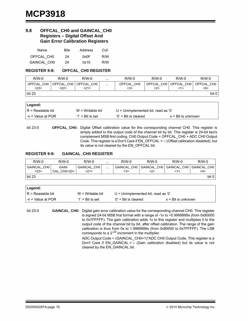
MCP3918
9.8 OFFCAL_CH0 and GAINCAL_CH0 Registers – Digital Offset And Gain Error Calibration Registers
Name Bits Address Cof.
OFFCAL_CH0 24 0x0F R/W
GAINCAL_CH0 24 0x10 R/W
REGISTER 9-8: OFFCAL_CH0 REGISTER
R/W-0 R/W-0 R/W-0 ... R/W-0 R/W-0 R/W-0 R/W-0
OFFCAL_CH0<23>
OFFCAL_CH0<22>
OFFCAL_CH0<21>
... OFFCAL_CH0<3>
OFFCAL_CH0<2>
OFFCAL_CH0<1>
OFFCAL_CH0<0>
bit 23 bit 0
Legend:
R = Readable bit W = Writable bit U = Unimplemented bit, read as ‘0’
-n = Value at POR ‘1’ = Bit is set ‘0’ = Bit is cleared x = Bit is unknown
bit 23-0 OFFCAL_CH0: Digital Offset calibration value for the corresponding channel CH0. This register issimply added to the output code of the channel bit by bit. This register is 24-bit two'scomplement MSB first coding. CH0 Output Code = OFFCAL_CH0 + ADC CH0 OutputCode. This register is a Don't Care if EN_OFFCAL = 0 (Offset calibration disabled), butits value is not cleared by the EN_OFFCAL bit.
REGISTER 9-9: GAINCAL_CH0 REGISTER
R/W-0 R/W-0 R/W-0 ... R/W-0 R/W-0 R/W-0 R/W-0
GAINCAL_CH0<23>
GAIN-CAL_CH0<22>
GAINCAL_CH0<21>
... GAINCAL_CH0<3>
GAINCAL_CH0<2>
GAINCAL_CH0<1>
GAINCAL_CH0<0>
bit 23 bit 0
Legend:
R = Readable bit W = Writable bit U = Unimplemented bit, read as ‘0’
-n = Value at POR ‘1’ = Bit is set ‘0’ = Bit is cleared x = Bit is unknown
bit 23-0 GAINCAL_CH0: Digital gain error calibration value for the corresponding channel CH0. This registeris signed 24-bit MSB first format with a range of -1x to +0.9999999x (from 0x80000to 0x7FFFFF). The gain calibration adds 1x to this register and multiplies it to theoutput code of the channel bit by bit, after offset calibration. The range of the gaincalibration is thus from 0x to 1.9999999x (from 0x80000 to 0x7FFFFF). The LSBcorresponds to a 2-23 increment in the multiplier.
ADC Output Code = (GAINCAL_CH0+1)*ADC CH0 Output Code. This register is aDon't Care if EN_GAINCAL = 0 (Gain calibration disabled) but its value is notcleared by the EN_GAINCAL bit.
DS20005287A-page 76 2014 Microchip Technology Inc.

MCP3918
9.9 SECURITY Register – Password and CRC-16 on Register Map
Name Bits Address Cof.
LOCK/CRC 24 0x1F R/W
REGISTER 9-10: LOCK/CRC REGISTER
R/W-1 R/W-0 R/W-1 R/W-0 R/W-0 R/W-1 R/W-0 R/W-1
LOCK<7> LOCK<6> LOCK<5> LOCK<4> LOCK<3> LOCK<2> LOCK<1> LOCK<0>
bit 23 bit 16
R/W-0 R/W-0 R/W-0 R/W-0 R/W-0 R/W-0 R/W-0 R/W-0
CRCREG<15> CRCREG<14> CRCREG<13> CRCREG<12> CRCREG<11> CRCREG<10> CRCREG<9> CRCREG<8>
bit 15 bit 8
R/W-0 R/W-0 R/W-0 R/W-0 R/W-0 R/W-0 R/W-0 R/W-0
CRCREG<7> CRCREG<6> CRCREG<5> CRCREG<4> CRCREG<3> CRCREG<2> CRCREG<1> CRCREG<0>
bit 7 bit 0
Legend:
R = Readable bit W = Writable bit U = Unimplemented bit, read as ‘0’
-n = Value at POR ‘1’ = Bit is set ‘0’ = Bit is cleared x = Bit is unknown
bit 23-16 LOCKn<7:0>: Lock Code for the writable part of the register mapLOCK<7:0> = PASSWORD = 0xA5 (Default value): The entire register map is writable. The
CRCREG<15:0> bits and the CRC Interrupt are cleared. No CRC-16 checksum on register map is calculated.
LOCK<7:0> different from 0xA5: The only writable register is the LOCK/CRC register. All other registers will appear as undefined while in this mode. The CRCREG checksum is calculated continuously and can generate interrupts if the CRC Interrupt EN_INT bit has been enabled. If a write to a register needs to be performed, the user needs to unlock the register map beforehand, by writing 0xA5 to the LOCK<7:0> bits.
bit 15-0 CRCREG<15:0>: CRC-16 Checksum that is calculated with the writable part of the register map as a message. This is a read-only 16-bit code. This checksum is continuously recalculated and updated every 10 DMCLK periods. It is reset to its default value (0x0000) when LOCK<7:0> = 0xA5.
2014 Microchip Technology Inc. DS20005287A-page 77

MCP3918
NOTES:
DS20005287A-page 78 2014 Microchip Technology Inc.
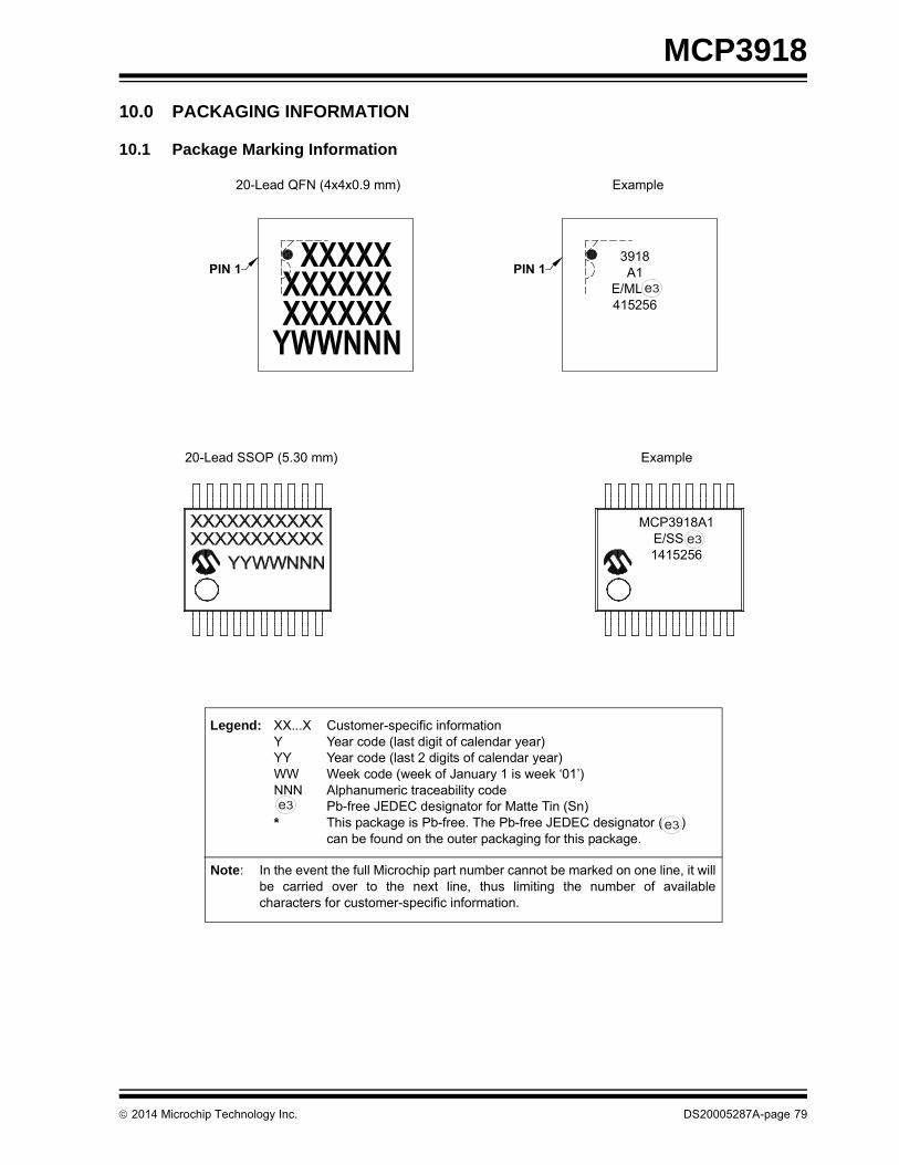
MCP3918
10.0 PACKAGING INFORMATION
10.1 Package Marking Information
Legend: XX...X Customer-specific informationY Year code (last digit of calendar year)YY Year code (last 2 digits of calendar year)WW Week code (week of January 1 is week ‘01’)NNN Alphanumeric traceability code Pb-free JEDEC designator for Matte Tin (Sn)* This package is Pb-free. The Pb-free JEDEC designator ( )
can be found on the outer packaging for this package.
Note: In the event the full Microchip part number cannot be marked on one line, it willbe carried over to the next line, thus limiting the number of availablecharacters for customer-specific information.
3e
3e
20-Lead QFN (4x4x0.9 mm) Example
PIN 1 PIN 13918A1
E/ML ^^415256
3e
20-Lead SSOP (5.30 mm) Example
MCP3918A1E/SS ^^1415256
3e
2014 Microchip Technology Inc. DS20005287A-page 79

MCP3918
��������� ���������������������������������� !!"�#$���%
�
���� &�� ��������!"�����#�$�%��&"��'������(�)"&�'"!&�)�����&�#�*�&����&�����&���#������� ���+�����!�!�*�!���"��&�#�,� ��'��!��������#�&���������������-�.���/��
:�;< :�!�����'��!���� ���&��������$��&����"��!�*��*�&�"&�&������!��-=< ��%��������'��!��(�"!"�����*�&�"&�&������(�%���%'�&����"�!�!�����
����& =�&���'!&��"��&����+����#�*���!(�����!��!���&��������������+�����������%���&������&�#��&��&&�<>>***�'��������'>���+�����
?��&! ��@@��- -����'��!���@�'�&! ��E EJ� ��K
E"')��%����! E ����&�� � ��/��:�;J������M����& � ��Q� ���� �����&��#%%� �� ���� ���� ���/;�&��&� ���+��!! �, ������-=J������U�#&� - �����:�;-$�!�#���#�U�#&� -� ��V� ���� ��Q�J������@���&� � �����:�;-$�!�#���#�@���&� �� ��V� ���� ��Q�;�&��&�U�#&� ) ���Q ���/ ��,�;�&��&�@���&� @ ��,� ���� ��/�;�&��&�&�-$�!�#���# X ���� Y Y
DEXPOSED
PAD
E
E2
2
1
N
TOP VIEW NOTE 1
N
L
K
b
e
D2
2
1
A
A1A3
BOTTOM VIEW
������� ������� ��*��� ;�����V:
DS20005287A-page 80 2014 Microchip Technology Inc.
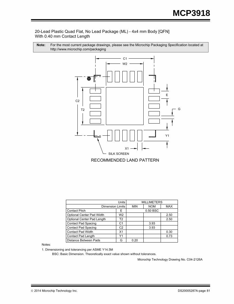
MCP3918
����& =�&���'!&��"��&����+����#�*���!(�����!��!���&��������������+�����������%���&������&�#��&��&&�<>>***�'��������'>���+�����
2014 Microchip Technology Inc. DS20005287A-page 81

MCP3918
��������� ���'()�*�'!���+����*��''��,�-�!!"�#$''+�%
���� &�� ��������!"�����#�$�%��&"��'������(�)"&�'"!&�)�����&�#�*�&����&�����&���#������� ��'��!��!�����#�-��#��&�����"#��'�#�%��!����&"!��!����#�%��!����&"!��!�!������&��$���#������''����!�#��,� ��'��!��������#�&���������������-�.���/��
:�;< :�!�����'��!���� ���&��������$��&����"��!�*��*�&�"&�&������!��-=< ��%��������'��!��(�"!"�����*�&�"&�&������(�%���%'�&����"�!�!�����
����& =�&���'!&��"��&����+����#�*���!(�����!��!���&��������������+�����������%���&������&�#��&��&&�<>>***�'��������'>���+�����
?��&! ��@@��- -����'��!���@�'�&! ��E EJ� ��K
E"')��%����! E ����&�� � ��V/�:�;J������M����& � Y Y ������#�#����+���� ���+��!! �� ��V/ ���/ ��Q/�&��#%%� �� ���/ Y YJ������U�#&� - ���� ��Q� Q�����#�#����+����U�#&� -� /��� /�,� /�V�J������@���&� � V��� ���� ��/�=&�@���&� @ ��// ���/ ���/=&���& @� ���/��-=@��#� ���+��!! � ���� Y ���/=&������ � �Z �Z QZ@��#�U�#&� ) ���� Y ��,Q
φ
LL1
A2c
eb
A1
A
1 2
NOTE 1
E1
E
D
N
������� ������� ��*��� ;������:
DS20005287A-page 82 2014 Microchip Technology Inc.

MCP3918
Note: For the most current package drawings, please see the Microchip Packaging Specification located at http://www.microchip.com/packaging
2014 Microchip Technology Inc. DS20005287A-page 83

MCP3918
NOTES:
DS20005287A-page 84 2014 Microchip Technology Inc.

2014 Microchip Technology Inc. DS20005287A-page 85
MCP3918
APPENDIX A: REVISION HISTORY
Revision A (May 2014)
• Original Release of this Document.

2014 Microchip Technology Inc. DS20005287A-page 86
MCP3918
PRODUCT IDENTIFICATION SYSTEM
To order or obtain information, e.g., on pricing or delivery, refer to the factory or the listed sales office.
Device: MCP3918A1: One Channel Analog Font End Converter
Address Options: XX A6 A5
A0 = 0 0
A1* = 0 1
A2 = 1 0
A3 = 1 1
* Default option. Contact Microchip factory for other address options
Tape and Reel: T = Tape and Reel
Temperature Range: E = -40°C to +125°C
Package: ML = 20-Lead Plastic Quad Flat, No Lead Package – 4x4 mm Body with 0.40 mm Contact Length (QFN)
SS = 20-Lead Plastic Shrink Small Outline – 5.30 mm Body (SSOP)
Examples:
a) MCP3918A1-E/ML: Address Option A1,Extended Temperature,20LD QFN package
b) MCP3918A1T-E/ML: Address Option A1,Tape and Reel,Extended Temperature,20LD QFN package
a) MCP3918A1-E/SS: Address Option A1,Extended Temperature,20LD SSOP package
b) MCP3918A1T-E/SS: Address Option A1,Tape and Reel,Extended Temperature,20LD SSOP package
PART NO. X
TemperatureRange
Device
/XX
Package
X
Tape andReel
XX
AddressOptions
Note the following details of the code protection feature on Microchip devices:
• Microchip products meet the specification contained in their particular Microchip Data Sheet.
• Microchip believes that its family of products is one of the most secure families of its kind on the market today, when used in the intended manner and under normal conditions.
• There are dishonest and possibly illegal methods used to breach the code protection feature. All of these methods, to our knowledge, require using the Microchip products in a manner outside the operating specifications contained in Microchip’s Data Sheets. Most likely, the person doing so is engaged in theft of intellectual property.
• Microchip is willing to work with the customer who is concerned about the integrity of their code.
• Neither Microchip nor any other semiconductor manufacturer can guarantee the security of their code. Code protection does not mean that we are guaranteeing the product as “unbreakable.”
Code protection is constantly evolving. We at Microchip are committed to continuously improving the code protection features of ourproducts. Attempts to break Microchip’s code protection feature may be a violation of the Digital Millennium Copyright Act. If such actsallow unauthorized access to your software or other copyrighted work, you may have a right to sue for relief under that Act.
Information contained in this publication regarding deviceapplications and the like is provided only for your convenienceand may be superseded by updates. It is your responsibility toensure that your application meets with your specifications.MICROCHIP MAKES NO REPRESENTATIONS ORWARRANTIES OF ANY KIND WHETHER EXPRESS ORIMPLIED, WRITTEN OR ORAL, STATUTORY OROTHERWISE, RELATED TO THE INFORMATION,INCLUDING BUT NOT LIMITED TO ITS CONDITION,QUALITY, PERFORMANCE, MERCHANTABILITY ORFITNESS FOR PURPOSE. Microchip disclaims all liabilityarising from this information and its use. Use of Microchipdevices in life support and/or safety applications is entirely atthe buyer’s risk, and the buyer agrees to defend, indemnify andhold harmless Microchip from any and all damages, claims,suits, or expenses resulting from such use. No licenses areconveyed, implicitly or otherwise, under any Microchipintellectual property rights.
2014 Microchip Technology Inc.
QUALITY MANAGEMENT SYSTEM CERTIFIED BY DNV
== ISO/TS 16949 ==
Trademarks
The Microchip name and logo, the Microchip logo, dsPIC, FlashFlex, KEELOQ, KEELOQ logo, MPLAB, PIC, PICmicro, PICSTART, PIC32 logo, rfPIC, SST, SST Logo, SuperFlash and UNI/O are registered trademarks of Microchip Technology Incorporated in the U.S.A. and other countries.
FilterLab, Hampshire, HI-TECH C, Linear Active Thermistor, MTP, SEEVAL and The Embedded Control Solutions Company are registered trademarks of Microchip Technology Incorporated in the U.S.A.
Silicon Storage Technology is a registered trademark of Microchip Technology Inc. in other countries.
Analog-for-the-Digital Age, Application Maestro, BodyCom, chipKIT, chipKIT logo, CodeGuard, dsPICDEM, dsPICDEM.net, dsPICworks, dsSPEAK, ECAN, ECONOMONITOR, FanSense, HI-TIDE, In-Circuit Serial Programming, ICSP, Mindi, MiWi, MPASM, MPF, MPLAB Certified logo, MPLIB, MPLINK, mTouch, Omniscient Code Generation, PICC, PICC-18, PICDEM, PICDEM.net, PICkit, PICtail, REAL ICE, rfLAB, Select Mode, SQI, Serial Quad I/O, Total Endurance, TSHARC, UniWinDriver, WiperLock, ZENA and Z-Scale are trademarks of Microchip Technology Incorporated in the U.S.A. and other countries.
SQTP is a service mark of Microchip Technology Incorporated in the U.S.A.
GestIC and ULPP are registered trademarks of Microchip Technology Germany II GmbH & Co. KG, a subsidiary of Microchip Technology Inc., in other countries.
All other trademarks mentioned herein are property of their respective companies.
© 2014, Microchip Technology Incorporated, Printed in the U.S.A., All Rights Reserved.
Printed on recycled paper.
ISBN: 978-1-63276-214-6
Microchip received ISO/TS-16949:2009 certification for its worldwide
DS20005287A-page 87
headquarters, design and wafer fabrication facilities in Chandler and Tempe, Arizona; Gresham, Oregon and design centers in California and India. The Company’s quality system processes and procedures are for its PIC® MCUs and dsPIC® DSCs, KEELOQ® code hopping devices, Serial EEPROMs, microperipherals, nonvolatile memory and analog products. In addition, Microchip’s quality system for the design and manufacture of development systems is ISO 9001:2000 certified.

DS20005287A-page 88 2014 Microchip Technology Inc.
AMERICASCorporate Office2355 West Chandler Blvd.Chandler, AZ 85224-6199Tel: 480-792-7200 Fax: 480-792-7277Technical Support: http://www.microchip.com/supportWeb Address: www.microchip.com
AtlantaDuluth, GA Tel: 678-957-9614 Fax: 678-957-1455
Austin, TXTel: 512-257-3370
BostonWestborough, MA Tel: 774-760-0087 Fax: 774-760-0088
ChicagoItasca, IL Tel: 630-285-0071 Fax: 630-285-0075
ClevelandIndependence, OH Tel: 216-447-0464 Fax: 216-447-0643
DallasAddison, TX Tel: 972-818-7423 Fax: 972-818-2924
DetroitNovi, MI Tel: 248-848-4000
Houston, TX Tel: 281-894-5983
IndianapolisNoblesville, IN Tel: 317-773-8323Fax: 317-773-5453
Los AngelesMission Viejo, CA Tel: 949-462-9523 Fax: 949-462-9608
New York, NY Tel: 631-435-6000
San Jose, CA Tel: 408-735-9110
Canada - TorontoTel: 905-673-0699 Fax: 905-673-6509
ASIA/PACIFICAsia Pacific OfficeSuites 3707-14, 37th FloorTower 6, The GatewayHarbour City, KowloonHong KongTel: 852-2943-5100Fax: 852-2401-3431
Australia - SydneyTel: 61-2-9868-6733Fax: 61-2-9868-6755
China - BeijingTel: 86-10-8569-7000 Fax: 86-10-8528-2104
China - ChengduTel: 86-28-8665-5511Fax: 86-28-8665-7889
China - ChongqingTel: 86-23-8980-9588Fax: 86-23-8980-9500
China - HangzhouTel: 86-571-8792-8115 Fax: 86-571-8792-8116
China - Hong Kong SARTel: 852-2943-5100 Fax: 852-2401-3431
China - NanjingTel: 86-25-8473-2460Fax: 86-25-8473-2470
China - QingdaoTel: 86-532-8502-7355Fax: 86-532-8502-7205
China - ShanghaiTel: 86-21-5407-5533 Fax: 86-21-5407-5066
China - ShenyangTel: 86-24-2334-2829Fax: 86-24-2334-2393
China - ShenzhenTel: 86-755-8864-2200 Fax: 86-755-8203-1760
China - WuhanTel: 86-27-5980-5300Fax: 86-27-5980-5118
China - XianTel: 86-29-8833-7252Fax: 86-29-8833-7256
China - XiamenTel: 86-592-2388138 Fax: 86-592-2388130
China - ZhuhaiTel: 86-756-3210040 Fax: 86-756-3210049
ASIA/PACIFICIndia - BangaloreTel: 91-80-3090-4444 Fax: 91-80-3090-4123
India - New DelhiTel: 91-11-4160-8631Fax: 91-11-4160-8632
India - PuneTel: 91-20-3019-1500
Japan - OsakaTel: 81-6-6152-7160 Fax: 81-6-6152-9310
Japan - TokyoTel: 81-3-6880- 3770 Fax: 81-3-6880-3771
Korea - DaeguTel: 82-53-744-4301Fax: 82-53-744-4302
Korea - SeoulTel: 82-2-554-7200Fax: 82-2-558-5932 or 82-2-558-5934
Malaysia - Kuala LumpurTel: 60-3-6201-9857Fax: 60-3-6201-9859
Malaysia - PenangTel: 60-4-227-8870Fax: 60-4-227-4068
Philippines - ManilaTel: 63-2-634-9065Fax: 63-2-634-9069
SingaporeTel: 65-6334-8870Fax: 65-6334-8850
Taiwan - Hsin ChuTel: 886-3-5778-366Fax: 886-3-5770-955
Taiwan - KaohsiungTel: 886-7-213-7830
Taiwan - TaipeiTel: 886-2-2508-8600 Fax: 886-2-2508-0102
Thailand - BangkokTel: 66-2-694-1351Fax: 66-2-694-1350
EUROPEAustria - WelsTel: 43-7242-2244-39Fax: 43-7242-2244-393Denmark - CopenhagenTel: 45-4450-2828 Fax: 45-4485-2829
France - ParisTel: 33-1-69-53-63-20 Fax: 33-1-69-30-90-79
Germany - DusseldorfTel: 49-2129-3766400
Germany - MunichTel: 49-89-627-144-0 Fax: 49-89-627-144-44
Germany - PforzheimTel: 49-7231-424750
Italy - Milan Tel: 39-0331-742611 Fax: 39-0331-466781
Italy - VeniceTel: 39-049-7625286
Netherlands - DrunenTel: 31-416-690399 Fax: 31-416-690340
Poland - WarsawTel: 48-22-3325737
Spain - MadridTel: 34-91-708-08-90Fax: 34-91-708-08-91
Sweden - StockholmTel: 46-8-5090-4654
UK - WokinghamTel: 44-118-921-5800Fax: 44-118-921-5820
Worldwide Sales and Service
03/25/14