mckinsey on semiconductors › ~ › media › mckinsey › industries...welcome to the seventh...
TRANSCRIPT

Number 7, October 2019
Creating value, pursuing innovation, and optimizing operations
McKinsey on Semiconductors

McKinsey on Semiconductors is written by experts and practitioners in McKinsey & Company’s Semiconductors Practice along with other McKinsey colleagues.
To send comments or request copies, email us: McKinsey_on_ Semiconductors@ McKinsey.com.
Cover image: © scanrail/Getty Images
Editorial Board: Ondrej Burkacky, Peter Kenevan, Abhijit Mahindroo
Editor: Eileen Hannigan
Art Direction and Design: Leff Communications
Data Visualization: Richard Johnson, Jonathon Rivait
Managing Editors: Heather Byer, Venetia Simcock
Editorial Production: Elizabeth Brown, Roger Draper, Gwyn Herbein, Pamela Norton, Katya Petriwsky, Charmaine Rice,John C. Sanchez, Dana Sand,Sneha Vats, Pooja Yadav, Belinda Yu
McKinsey Practice Publications
Editor in Chief: Lucia Rahilly
Executive Editors: Michael T. Borruso, Bill Javetski, Mark Staples
Copyright © 2019 McKinsey & Company. All rights reserved.
This publication is not intended to be used as the basis for trading in the shares of any company or for undertaking any other complex or significant financial transaction without consulting appropriate professional advisers.
No part of this publication may be copied or redistributed in any form without the prior written consent of McKinsey & Company.

Table of contents
3
16
27
38
47What’s next for semiconductor profits and value creation?
Semiconductor profits have been strong over the past few years. Could recent changes within the industry stall their progress?
Artificial-intelligence hardware: New opportunities for semiconductor companies
Artificial intelligence is opening the best opportunities for semiconductor companies in decades. How can they capture this value?
Blockchain 2.0: What’s in store for the two ends —semiconductors (suppliers) and industrials (consumers)?
Ten years after blockchain’s inception, it is presenting new opportunities for both suppliers, such as semiconductor companies, and consumers, such as industrials.
Rethinking car software and electronics architecture
As the car continues its transition from a hardware-driven machine to a software-driven electronics device, the auto industry’s competitive rules are being rewritten.
How will changes in the automotive-component market affect semiconductor companies?
The rise of domain control units (DCUs) will open new opportunities for semiconductor companies.
50
57
63
Right product, right time, right location: Quantifying the semiconductor supply chain
Problems along the semiconductor supply chain are difficult to diagnose. A new metric can help companies pinpoint performance issues.
Reducing indirect labor costs at semiconductor companies
Digital tools could bring new productivity and efficiency gains to indirect functions. Why do semiconductor companies hesitate to use them?
Taking the next leap forward in semiconductor yield improvement
By prioritizing improvements in end-to-end yield, semiconductor companies can better manage cost pressures and sustain higher profitability. The path forward involves advanced analytics.

Welcome to the seventh edition of McKinsey on Semiconductors. This publication appears at a time when our world is being transformed by the growth of artificial intelligence (AI), machine learning, and other innovative technologies. The pace of change is so fast that leading-edge products today may seem dated within a year. In this constantly evolving landscape, only one thing is certain: semiconductor companies will enable some of the most important technological leaps.
Many semiconductor companies are already benefiting from the innovative offerings, with the sector showing strong and rising profits over the past few years. But there may be challenges ahead, since companies that want to remain industry leaders must continue to increase their R&D investments. With costs in labor and other areas rising, some semiconductor companies may have difficulty finding additional funds for innovation. Moreover, some customers are already designing chips internally, and others may follow—a trend that could decrease sales. These concerns, and possible solutions, are the focus of the first article in this issue: “What’s next for semiconductor profits and value creation?”
Other articles discuss recent technological trends that are increasing demand for chips. In “Artificial-intelligence hardware: New opportunities for semiconductor companies,” the authors explore how the rise of AI could help players capture more value. Overall, semiconductor growth from AI may be five times greater than growth from other sources. Opportunity is also the central theme of “Blockchain 2.0: What’s in store for the two ends—semiconductors (suppliers) and industrials (consumers)?” As this article describes, blockchain’s role in cryptocurrency and its potential growth as a business application may accelerate demand for chips. The extent of the change, as well as the timing, is still uncertain, but semiconductor leaders that monitor developments could have an advantage if blockchain takes off.
This issue also contains two articles that discuss a technology leap that has intrigued consumers: the rise of autonomous vehicles. “Rethinking car software and electronics architecture” explores how sensors and other automotive components may evolve, since these changes could influence chip demand. One specific shift—the rise of domain control units—is described in another article: “How will changes in the automotive-component market affect semiconductor companies?”
While all of these developments are exciting, semiconductor companies also have to deal with some stubborn problems that have plagued their businesses for years. Companies will discover a new approach to eliminating late shipments in “Right product, right time, right location: Quantifying the semiconductor supply chain.” Similarly, they will learn about strategies for decreasing one of their largest costs in
“Reducing indirect labor costs at semiconductor companies.” The final article, “Taking the next leap forward in semiconductor yield improvement,” will help companies use analytics and other strategies to optimize production in both line and die processes.
McKinsey on Semiconductors is designed to help industry executives navigate the road ahead and achieve continued growth. We hope that you find these articles helpful.
Introduction
Ondrej BurkackyPartner
Peter KenevanSenior partner
Abhijit MahindrooPartner
2 McKinsey on Semiconductors Number 7, October 2019
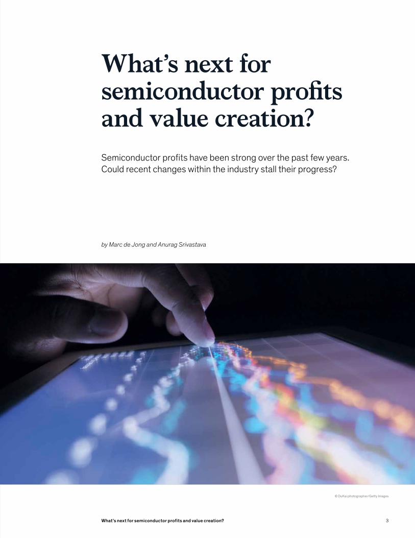
What’s next for semiconductor profits and value creation?
What’s next for semiconductor profits and value creation?Semiconductor profits have been strong over the past few years. Could recent changes within the industry stall their progress?
© DuKai photographer/Getty Images
by Marc de Jong and Anurag Srivastava
3

Outside Silicon Valley, the semiconductor industry’s recent profitability seems unsurprising. The general assumption is that these players, like other tech companies, have long benefited from the rise of PCs, smartphones, and other devices. But insiders know that the industry’s good fortune is a relatively recent phenomenon. While software players were achieving record gains for most of the past two decades, most semiconductor companies achieved limited economic profitability. Overall, only microprocessor companies and some fabless players could count on consistently strong returns, above the cost of capital.
Now the semiconductor sector is showing strong and rising profits. What’s more, companies in virtually all subsegments are winning big. To discover how semiconductor companies engineered this turnaround, we analyzed trends related to economic profit (see sidebar, “Economic
profit”).¹ With this information, we wanted to answer an even more important question: What can semiconductor players do to ensure that the recent gains are not a blip but the emergence of a new industry norm?
A decade of change: How value creation has evolved within the semiconductor industryOnly ten years ago, the semiconductor industry had mediocre returns. Although many companies were generating value, they lagged far behind their counterparts in other industries. But a much different story has unfolded over the past five years, with the semiconductor industry reporting record gains. In 2017 alone, it generated $97 billion in economic profit—more than a threefold increase from the $28 billion captured in 2013 (Exhibit 1).
Exhibit 1
McKinsey on Semiconductors 2018What’s next semiconductorsExhibit 1 of 10
¹ Figures may not sum, because of rounding.² About 273 companies across all industry subsegments. Source: Annual reports; Semiconductor CPC database; McKinsey Corporate Performance Center
Economic-pro�t1 value creation for semiconductor industry² (excluding goodwill), $ billion
2010 2011 2012 2013 2014 2015 2016 2017
42 4030 34
4752
59
99
–4–10 –12
–7 –5 –5
Cumulative positive economic pro�t for companies Cumulative negative economic pro�t for companies
–5 –3
38 30 18 28 42 47 54 97
Total economic pro�t, $ billion
From a value-creation perspective, 2017 was a record year for the semiconductor industry.
1 Economic profit equals the net operating profit after tax minus the capital charge (the invested capital, excluding goodwill—the amount of a purchase that exceeds the value of the assets involved) at previous year-end multiplied by the weighted average cost of capital.
4 McKinsey on Semiconductors Number 7, October 2019

What’s next for semiconductor profits and value creation?
Economic profit
When we looked at value creation within the semiconductor industry, we deliberately restricted our analysis to economic profit, which is a periodic measure of value creation. In simplest terms, it is the amount left over after subtracting the cost of capital from net operating profit. The formula for computing it is as follows:
We chose to focus on economic profit because this metric comprehensively captures both profitability and the opportunity cost for the capital deployed. It also allowed us to perform reliable benchmark analyses for companies that followed many different business models. We only considered operating assets and excluded goodwill and other M&A intangibles. This approach allowed us to compare operating performance for different companies, regardless of whether their growth occurred organically or arose from a merger. For the years 2013 through 2017, however, we conducted two analyses: one factored in goodwill, and one did not (similar to the long-term analysis for 1997 through 2017). We conducted the two analyses to determine if the recent surge in M&A activity had a significant effect on results.
Economic profit = return on
invested capital (ROIC)
x invested capital x invested
capital – weighted average cost of capital (WACC)
From 2012 to 2016, the semiconductor sector ranked tenth out of 59 major industries for value creation, placing it in the top 20 percent. That represents a big jump from the period from 2002 through 2006, when it ranked 18th.
5

From 2012 to 2016, the semiconductor sector ranked tenth out of 59 major industries for value creation, placing it in the top 20 percent. That represents a big jump from the period from 2002 through 2006, when it ranked 18th. While the semiconductor sector still lags far behind software, which was second only to biotechnology, it now outranks IT services, aerospace and defense, chemical, and many other major sectors for value creation.
Strong global economic growth since the 2008 recession has propelled the semiconductor industry’s revenues, but an even more important factor involves the continued rise of the technology sector. Companies such as Alibaba, Amazon,
Facebook, Google, and Tencent become more important to the global economy every year. These companies constantly introduce product or technology upgrades to remain competitive, and they need chips to enable such advances. Semiconductor companies have also benefited from increased digitization and cloud use across other industries, both of which accelerate chip demand.
In addition to these traditional revenue drivers, some recent technology innovations, including the Internet of Things, artificial-intelligence (AI) applications, and blockchain technology, have created new opportunities for semiconductor companies to capture value. Advances in the automotive industry, including vehicle electrification and the development of self-driving cars, are also increasing chip demand. Such innovations are transforming how much value semiconductor companies capture from the technology stack. With AI applications, for instance, they could potentially achieve a larger share of total value than they did with PCs and mobile phones.
Value trends within the semiconductor industryThe rise in economic profit is not the only big shift within the semiconductor industry. As we reviewed the trends, we also found that value distribution has changed. From 1997 to 2012, the cumulative positive economic profit across segments was $161.5 billion. But some segments also lost value (Exhibit 2).
Overall, value was highly concentrated in a few areas (Exhibit 3). The microprocessor subsegment generated the most value, followed by fabless. Together, they created almost all value in the industry, with all other subsegments roughly breaking even when their results were totaled.
Exhibit 2
McKinsey on Semiconductors 2018What’s next semiconductorsExhibit 2 of 10
Source: Annual reports; Semiconductor CPC database; McKinsey Corporate Performance Center
1997–2012
2013–17
1997–2012
2013–17
Economic-pro�t value creation across subsegments (excluding goodwill), cumulative, $ billion
Average annual economic pro�t (excluding goodwill), $ billion
Cumulative negative economic pro�t across subsegments
Cumulative positive economic pro�t across subsegments
161.5
7.9
53.4
–38.7
–0.6
+575%
267.5
Value creation has migrated to almost all subsegments.
6 McKinsey on Semiconductors Number 7, October 2019

What’s next for semiconductor profits and value creation?
Exhibit 3
McKinsey on Semiconductors 2018What’s next semiconductorsExhibit 3 of 10
¹ Figures may not sum, because of rounding.² Intellectual property.3 Integrated device manufacturer. Source: Annual reports; Semiconductor CPC database; McKinsey Corporate Performance Center
Economic-pro�t1 value creation by subsegment (excluding goodwill), 1997–2012 cumulative, $ billion
Cumulative positive economic pro�t for companies Cumulative negative economic pro�t for companies
From 1997 through 2012, the microprocessor and fabless subsegments created the most value.
ACapital
equipment
BElectronic-
designautomation
CIP2
E Micro-
processor
FMemory
GAnalogIDM3
HDiversi�ed
IDM
IOtherIDM
JFoundry
KPackaging
andassembly
42
62.5
22.4
82.4
38.1
15.2 15.6 4.7 1.120.9
–0.2 –0.3
1.74.1
–8.6 –7.6 –5.4
–47.6
–1.0
–36.4
–8.0 –2.2
–12.6
1.53.813.8 57.1 74.8 –9.5 14.2 –20.8 –3.3 8.3 –1.1
DFabless
Total economic pro�t, $ billion
A) AMAT, ASML, KLA-Tencor; B) Synopsys, Cadence, Mentor graphics: C) ARM, Rambus, Spansion; D) Qualcomm, Mediatek, Xilinx; E) Intel; F) Samsung, Sandisk; G) Linear, Analog, Maxxim; H) TI, ON, NXP; I) Microchip, Powertech, Faraday; J) TSMC; K) Silicon-ware, Monolithic power.
Top companies for economic pro�t, by subsegment
From 1997 to 2012, the cumulative positive economic profit across segments was $161.5 billion. But some segments also lost value.
7

McKinsey on Semiconductors 2018What’s next semiconductorsExhibit 4 of 10
42
77.6
26.9
39.7
59.7
13.1
27.05.3
0.9
29.2
–0.10
1.93.3
–3.3–0.4–1.6 –1.2 –0.2 –2.7 –3.3 –1.5
–3.3
1.83.323.6 76.0 39.3 58.4 12.9 24.3 2.0 25.9 –0.6
ACapital
equipment
BElectronic-
designautomation
CIP2
EMicro-
processor
FMemory
GAnalogIDM3
HDiversied
IDM
IOtherIDM
JFoundry
KPackaging
andassembly
DFabless
Total economic pro�t, $ billion
¹ Figures may not sum, because of rounding.² Intellectual property.3 Integrated device manufacturer. Source: Annual reports; Semiconductor CPC database; McKinsey Corporate Performance Center
Economic-pro�t1 value creation by subsegment (excluding goodwill), 2013–17 cumulative, $ billion
Cumulative positive economic prot for companies Cumulative negative economic prot for companies
From 2013 through 2017, almost all subsegments demonstrated economic pro�t.
A) AMAT, ASML, Lam Research; B) Synopsys, Cadence, Mentor graphics; C) ARM, Rambus, CEVA; D) Broadcomm, Qualcomm, Apple; E) Intel; F) Samsung, SK Hynix, Sandisk; G) Analog, Skyworks, Linear; H) TI, Toshiba, NXP; I) Microchip, Nu�are, Fingerprint; J) TSMC; K) ASE, Silicon-ware.
Top companies for economic pro�t, by subsegment
From 2013 to 2017, by contrast, nearly all subsegments recorded positive economic profit (Exhibit 4). Fabless was the best performer during this period, with memory in second place. The microprocessor subsegment came in third, down from the top ranking it held from 1997 to 2012. This shift occurred partly because PCs—key drivers of microprocessor demand—have seen much lower growth than smartphones and tablets, which often rely on chips designed by fabless players. Memory players have benefited from less oversupply, resulting in higher average sales prices and operating margins.
Several factors may contribute to the greater distribution of value, including industry consolidation. First, many large conglomerates have divested their semiconductor units over the past ten years to reduce R&D investment and capital expenditures. Meanwhile, the industry has also undergone a wave of M&A across segments. The number of semiconductor companies fell from 208 in 2012 to 173 by 2017 (Exhibit 5). The fabless subsegment saw the most consolidation, followed by analog integrated device manufacturers and diversified integrated device manufacturers, but the drop in companies is notable in all sectors, including memory.
Exhibit 4
8 McKinsey on Semiconductors Number 7, October 2019

What’s next for semiconductor profits and value creation?
Exhibit 5
Because there’s greater scale within subsegments, companies have more resources to invest in innovation and operating improvements. Their large size also helps them rebound when downturns occur in this highly cyclical industry, since they can take advantage of economies of scale and rely on more designs than in the past for their revenues. If one customer leaves, their bottom-line will not see the same hit as a smaller player with only a few accounts. Overall, down cycles have been milder and peaks have been higher within the semiconductor industry over the past few years (Exhibit 6). Even when we factored goodwill—the amount of a purchase that exceeds the book value of the assets involved—into the calculation for the past five years, economic profit remained high. The fabless, memory, and microprocessor subsegments retained their
top three ranking. Results for value creation were similar across most other subsegments, although some notable declines occurred. For instance, in the microprocessor subsegment, the positive cumulative economic profit for the period from 2013 to 2017 would be reduced from $39.7 billion to $28.3 billion if goodwill is included. Since all semiconductor subsegments have engaged in M&A to a similar extent, it is not surprising that the relative rankings remained similar.
Potential challenges: The rise of in-house chip designAfter five successful years, semiconductor leaders across the industry have become a bit less optimistic about their prospects. Next to global tensions (hitting the semiconductor sector significantly, given the international value chains),
McKinsey on Semiconductors 2018What’s next semiconductorsExhibit 5 of 10
2012 2013A
2014B
2015C
2016D
2017E
103
208
114 130119 123 128
206 202187 184 173
10592
72 6861
45
Economic-pro�t value creation by number of companies, 2012–17 (all subsegments)
Companies with cumulative positive economic pro�t Companies with cumulative negative economic pro�t
Industry consolidation over the past ve years has likely contributed to improved pro tability.
A) Mindspeed Tech: Acquired by MACOM, Mtekvision Assets: Became private, Transwitch Corp: Filed for bankruptcy; B) International Recti�er: Acquired by In�neon Tech, Supertex: Acquired by Microchip Technology; C) Altera Corp: Acquired by Intel, IBM Microelectronics: Acquired by GlobalFoundries, Spansion: Merged with Cypress; D) Actions Semiconductor: Became Private, Anadigics: Acquired by II-VI Inc., Fairchild Semicon: Acquired by ON; E) Applied Micro Circuits: Acquired by MACOM
Major deals or bankruptcies by subsegment
Source: Annual reports; Semiconductor CPC database; McKinsey Corporate Performance Center
9

one trend is generating new questions: the continued rise of in-house chip design at some of the semiconductor industry’s largest customers.
This shift may be most prominent at Apple. While the company still relies on external providers for PC chips, it uses in-house designers to make the core chips for the iPhone, AppleTV, iWatch, and some other offerings. Apple then outsources chip manufacture to foundries. The company gains several advantages by taking this path:
— Improved customer experience. Apple wants to optimize the customer experience and ensure that it is consistent across devices. While an external provider could create custom designs to meet these goals, an in-house team is more likely to satisfy the company’s exacting specifications and possess the necessary technical knowledge.
— Competitive differentiation. By developing proprietary technology, Apple prevents other companies from replicating its customer experience.
— Insight into road maps. In-house creation gives Apple firsthand insight into processing-technology capabilities, allowing it to create more accurate product road maps and enabling superior launch planning for new products. For each offering, it can specify how and when it must update other technology elements to complement the processor.
— Negotiating leverage. The sheer volume of chips designed in-house provides a strong negotiating position with foundries.
While Apple has conducted in-house work for many years, the scale, extent, and impact of these
Exhibit 6
McKinsey on Semiconductors 2018What’s next semiconductorsExhibit 6 of 10
Source: Annual reports; Semiconductor CPC database; McKinsey Corporate Performance Center
Economic-pro�t value creation by all subsegments (excluding goodwill), $ billion
Cumulative positive economic pro�t for companies Cumulative negative economic pro�t for companies
Within the semiconductor industry, down cycles have been milder and peaks have been higher in past few years.
1997 2000 2010 2017
–40
–20
0
20
40
60
80
100
–40
–20
0
20
40
60
80
100
10 McKinsey on Semiconductors Number 7, October 2019
What’s next for semiconductor profits and value creation?
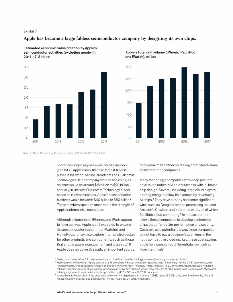
Exhibit 7
McKinsey on Semiconductors 2018What’s next semiconductorsExhibit 7 of 10
02011 2013 2015 2017
0.5
1.0
1.5
2.0
2.5
3.0
3.5
2011 2013 2015 20170
50
100
150
200
250
300
Source: Alphr; Bloomberg; Business Insider; IHS Markit; S&P Capital IQ
Estimated economic value creation by Apple’s semiconductor activities (excluding goodwill), 2011–17, $ billion
Apple has become a large fabless semiconductor company by designing its own chips.
Apple’s total unit volume (iPhone, iPad, iPod, and iWatch), million
operations might surprise even industry insiders (Exhibit 7). Apple is now the third largest fabless player in the world, behind Broadcom and Qualcomm Technologies. If the company were selling chips, its revenue would be around $15 billion to $20 billion annually, in line with Qualcomm Technology’s. And based on current multiples, Apple’s semiconductor business would be worth $40 billion to $80 billion.² These numbers speak volumes about the strength of Apple’s internal chip operations. Although shipments of iPhones and iPads appear to have peaked, Apple is still expected to expand its semiconductor footprint for iWatches and HomePods. It may also explore internal chip design for other products and components, such as those that enable power management and graphics.³ If Apple does go down this path, an important source
of revenue may further shift away from stand-alone semiconductor companies.
Many technology companies with deep pockets have taken notice of Apple’s success with in-house chip design. Several, including large cloud players, are beginning to follow its example by developing AI chips.⁴ They have already had some significant wins, such as Google’s tensor-processing unit and Amazon’s Graviton and Inferentia chips, all of which facilitate cloud computing.⁵ In-house creation allows these companies to develop customized chips that offer better performance and security. Costs are also potentially lower, since companies do not have to pay a designer’s premium. In the hotly competitive cloud market, these cost savings could help companies differentiate themselves from their rivals.
2 Based on a three- to fourfold revenue multiple of core Qualcomm Technology business (licensing business excluded).3 Mark Gurman and Ian King, “Apple plans to use its own chips in Macs from 2020, replacing Intel,” Bloomberg, April 2, 2018, bloomberg.com.4 Richard Waters, “Facebook joins Amazon and Google in AI chip race,” Financial Times, February 18, 2019, ft.com; Argam Atashyan, “Amazon
releases machine learning chips, namely Inferentia and Graviton,” Gizchina Media, November 29, 2018, gizchina.com; Jordan Novet, “Microsoft is hiring engineers to work on A.I. chip design for its cloud,” CNBC, June 11, 2018, cnbc.com.
⁵ Jordan Novet, “Microsoft is hiring engineers to work on A.I. chip design for its cloud,” CNBC, June 11, 2018, cnbc.com; Tom Simonite, “New at Amazon: Its own chips for cloud computing,” Wired, November 27, 2018, wired.com.
11

The development of ARM reference architectures, combined with the latest process improvements at state-of-the-art foundries, could now open the door to other tech companies that want to move design in-house—even those without deep pockets. If more companies begin designing chips in-house, the semiconductor industry will confront a new type of competitor—and that could have a long-term impact on demand and profitability.
Looking ahead: Investor expectationsEconomic profit is strongly correlated with total returns to shareholders (TRS) across industries. Overall, the semiconductor industry’s TRS has declined about 10 percent since its peak in late 2018, partly because investors are worried that the weakening macroeconomic environment could affect semiconductor demand (Exhibit 8).
A look at earnings multiples might suggest that investors are even less optimistic about the industry’s long-term growth prospects. But it’s more likely that they recognize that 2018 profit-ability for semiconductors was significantly higher when it reached the top of the cycle than it had been in past years. Even as profits inevitably trend downward, investors still expect them to reach historic levels.
As for the subsegments, fabless now has the highest multiple, suggesting that investors think it will remain more profitable and might undergo additional M&A, which would increase its resilience (Exhibit 9). Memory, by contrast, has a low multiple, even though this subsegment has recently generated record profits. Investors may be concerned that this segment is more commoditized and therefore subject to sharper cyclic declines.
Exhibit 8
McKinsey on Semiconductors 2018What’s next semiconductorsExhibit 8 of 10
Source: Annual reports; S&P Capital IQ; Semiconductor CPC database
Industry total returns to shareholders for the largest subsegments, index (Dec 31, 2012 = 100)
Total returns to shareholders have been strong within semiconductors.
Diversi�ed integrated device manufacturer
Fabless
Foundry
S&P 500
Memory
50
100
150
200
250
300
350
400
450
Q1
2013
Q1
2014
Q1
2015
Q1
2016
Q1
2017
Q1
2018
Q1
2019
12 McKinsey on Semiconductors Number 7, October 2019

What’s next for semiconductor profits and value creation?
Fabless also has the highest enterprise value and is now the largest subsegment by far (Exhibit 10). Its ability to capture the highest economic profit, strong near-term growth prospects, and potential resiliency all contribute to higher investor expectations.
Potential strategies for semiconductor companiesGiven the current landscape, semiconductor companies must accelerate value creation. Four actions seem essential:
— Creating strong road maps for leading customers. Semiconductor companies have long recognized the importance of delivering winning road maps for chip design, but the stakes are now higher than ever. In the past, customers that did not like a proposed road map might go to a
competitor for their design needs. Such losses hurt, but they were often temporary because customers often came back to the original company for future designs. Now if customers are dissatisfied with a road map, they might move design capabilities in-house, resulting in a permanent loss of business.
— Using M&A in moderation. The semiconductor industry is still fragmented in many subsegments, and industry consolidation still makes sense. The best strategy involves programmatic M&A, in which companies acquire at least one company a year, spending an average of 2 to 5 percent of their market capitalization, with no single deal accounting for more than 30 percent of their market capitalization.⁶ These deals allow players
Exhibit 9
McKinsey on Semiconductors 2018What’s next semiconductorsExhibit 9 of 10
3 2 1 –1 1 0 N/A⁴
Micro-processor
Capitalequipment
AnalogIDM
MemoryDiversi�edIDM²
FoundryFabless
1514
12
11 10 10
3
¹ Earnings before interest, taxes, and amortization; market data as of Dec 31, 2018.² Integrated device manufacturer.³ Compound annual growth rate.⁴ Memory industry reached the peak of the valuation cycle in 2018 with extraordinarily high margins. Margin decline is imminent for the sector and is included in the sector valuation. At 2018 margins, valuation cannot be reconciled with topline decline alone.
Source: Annual reports; Semiconductor CPC database; McKinsey Corporate Performance Center
Enterprise value/EBITA¹ ratio, 2018
Performance expectations are highest for the fabless subsegment.
Implied long-term organic growth at 2018 margins, % CAGR³
6 Chris Bradley, Martin Hirt, and Sven Smit, Strategy Beyond the Hockey Stick: People, Probabilities, and Big Moves to Beat the Odds, first edition, Hoboken, NJ: John Wiley & Sons, 2018.
13

to branch into adjacent areas to strengthen their competitive position. Deals that involve companies that only offer similar products will not produce as much value. One factor to consider when contemplating a deal is the value that it will bring to customers on measures such as price, quality, and performance. If an M&A
deal could improve any of these areas, it will help the companies create a more compelling road map that positions them for future success. But companies that undertake M&A must avoid falling into the trap of paying too much for goodwill, or else they risk destroying value.
Exhibit 10
McKinsey on Semiconductors 2018What’s next semiconductorsExhibit 8 of 10
Enterprise-value distribution across the semiconductor subsegments, % share
Fabless captures the most shareholder value across subsegments.
Microprocessors17
Capitalequipment
12
AnalogIDM
5
Others²7
Memory7
Diversi�edIDM¹
15
Foundry13
Fabless25
100% = $1.5 trillion
Note: Figures may not sum, because of rounding.¹ Integrated device manufacturer.² Includes intellectual property, electronic-design automation, packaging and assembly, and other IDM (discrete, opto, microcontroller unit). Source: S&P Capital IQ; McKinsey analysis
14 McKinsey on Semiconductors Number 7, October 2019

What’s next for semiconductor profits and value creation?
— Maintaining price discipline across the cycle. The large companies that have emerged from deal making have the resources required to create leading-edge chips. But they will only win if they focus on smart capacity planning and maintain relatively stable prices across economic cycles, even if demand slows.
— Preparing for vertical integration among tech giants. Many large tech players may try to acquire small niche companies, especially if they have desirable intellectual property, so they can increase their semiconductor capabilities. Other large players may choose to license their technologies, rather than buying
chips, or to exit certain areas altogether instead of operating subscale.⁷
The semiconductor industry’s recent move to value creation is impressive, but companies cannot assume that the strong profits will continue indefinitely. The move to in-house chip design among their most important customers could hit their bottom lines hard. While the pace and extent of this shift are still unknown, the best companies will begin preparing now by revamping their strategies.
Copyright © 2019 McKinsey & Company. All rights reserved.
Marc de Jong is a partner in McKinsey’s Amsterdam office, and Anurag Srivastava is an alumnus of the New York office.
7 Benjamin Mayo, “Apple licenses Dialog power management tech, and hires 300 engineers, to develop more custom iPhone chips,” 9to5Mac, October 10, 2018, 9to5mac.com.
15

Artificial-intelligence hardware: New opportunities for semiconductor companiesArtificial intelligence is opening the best opportunities for semi-conductor companies in decades. How can they capture this value?
© DuKai photographer/Getty Images
by Gaurav Batra, Zach Jacobson, Siddarth Madhav, Andrea Queirolo, and Nick Santhanam
16 McKinsey on Semiconductors Number 7, October 2019

Artificial-intelligence hardware: New opportunities for semiconductor companies
Software has been the star of high tech over the past few decades, and it’s easy to understand why. With PCs and mobile phones, the game-changing innovations that defined this era, the architecture and software layers of the technology stack enabled several important advances. In this environment, semiconductor companies were in a difficult position. Although their innovations in chip design and fabrication enabled next-generation devices, they received only a small share of the value coming from the technology stack—about 20 to 30 percent with PCs and 10 to 20 percent with mobile.
But the story for semiconductor companies could be different with the growth of artificial intelligence (AI). Many AI applications have already gained a wide following, including virtual assistants that manage our homes and facial-recognition programs that track criminals. These diverse solutions, as well as other emerging AI applications, share one common feature: a reliance on hardware as a core enabler of innovation, especially for logic and memory functions.
What will this development mean for semiconductor sales and revenues? And which chips will be most important to future innovations? To answer these questions, we reviewed current AI solutions and the technology that enables them. We also examined opportunities for semiconductor companies across the entire technology stack. Our analysis revealed three important findings about value creation:
— AI could allow semiconductor companies to capture 40 to 50 percent of total value from the technology stack, representing the best opportunity they’ve had in decades.
— Storage will experience the highest growth, but semiconductor companies will capture the most value in compute, memory, and networking.
— To avoid mistakes that limited value capture in the past, semiconductor companies must undertake a new value-creation strategy that focuses on enabling customized, end-to-end solutions for specific industries, or “microverticals.”
By keeping these beliefs in mind, semiconductor leaders can create a new road map for winning in AI.
This article begins by reviewing the opportunities that they will find across the technology stack, focusing on the impact of AI on hardware demand at data centers and the edge (computing that occurs with devices, such as self-driving cars). It then examines specific opportunities within compute, memory, storage, and networking. The article also discusses new strategies that can help semiconductor companies gain an advantage in the AI market, as well as issues they should consider as they plan their next steps.
The AI technology stack will open many opportunities for semiconductor companiesAI has made significant advances since its emergence in the 1950s, but some of the most important developments have occurred recently as developers created sophisticated machine-learning (ML) algorithms that can process large data sets, “learn” from experience, and improve over time. The greatest leaps came in the 2010s because of advances in deep learning (DL), a type of ML that can process a wider range of data, requires less data preprocessing by human operators, and often produces more accurate results.
To understand why AI is opening opportunities for semiconductor companies, consider the technology stack (Exhibit 1). It consists of nine discrete layers that allow the two activities that enable AI applications: training and inference (see sidebar “Training and inference”). When developers are trying to improve training and inference, they often encounter roadblocks related to the hardware layer, which includes storage, memory, logic, and networking. By providing next-generation accelerator architectures, semiconductor companies could increase computational efficiency or facilitate the transfer of large data sets through memory and storage. For instance, specialized memory for AI has 4.5 times more bandwidth than traditional memory, making it much better suited to handling the vast stores of big data that AI applications require. This performance improvement is so great that many customers would be more willing to pay the higher price that specialized memory requires (about $25 per gigabyte, compared with $8 for standard memory).
17

AI will drive a large portion of semiconductor revenues for data centers and the edgeWith hardware serving as a differentiator in AI, semiconductor companies will find greater demand for their existing chips, but they could also profit by developing novel technologies, such as workload-specific AI accelerators (Exhibit 2). We created a model to estimate how these AI opportunities would affect revenues and to determine whether AI-related chips would constitute a significant portion of future demand (see sidebar “How we estimated value” for more information on our methodology).
Our research revealed that AI-related semicon-ductors will see growth of about 18 percent annually over the next few years—five times greater than the rate for semiconductors used in non-AI applications
(Exhibit 3). By 2025, AI-related semiconductors could account for almost 20 percent of all demand, which would translate into about $65 billion in revenue. Opportunities will emerge at both data centers and the edge. If this growth materializes as expected, semiconductor companies will be positioned to capture more value from the AI technology stack than they have obtained with previous innovations—about 40 to 50 percent of the total.
AI will drive most growth in storage, but the best opportunities for value creation lie in other segmentsWe then took our analysis a bit further by looking at specific opportunities for semiconductor players within compute, memory, storage, and networking.
Exhibit 1
McKinsey on Semiconductors 2018Artificial intelligence semiconductorsExhibit 1 of 6
The technology stack for arti�cial intelligence (AI) contains nine layers.
¹ Dynamic random access memory.² Not AND.³ CPU = central processing unit, GPU = graphics-processing unit, FPGA = �eld programmable gate array, ASIC = application-speci�c integrated circuit. Source: Expert interviews; literature search
Technology Stack De�nition
Services Solution and use case
Data typesTraining
MethodsPlatform
Architecture
Algorithm
Framework
Interface systemsInterface
Head nodeHardware
Accelerator
Integrated solutions that include training data, models, hardware, and other components (eg, voice-recognition systems)
Data presented to AI systems for analysis
Techniques for optimizing weights given to model inputs
Structured approach to extract features from data (eg, convolutional or recurrent neural networks)
A set of rules that gradually modi�es the weights given to certain model inputs within the neural network during training to optimize inference
Software packages to de�ne architectures and invoke algorithms on the hardware through the interface
Systems within framework that determine and facilitate communication pathways between software and underlying hardware
Hardware unit that orchestrates and coordinates computations among accelerators
Silicon chip designed to perform highly parallel operations required by AI; also enables simultaneous computations
Memory• Electronic data repository for
short-term storage during processing
• Memory typically consists of DRAM1
Storage• Electronic repository for long-term
storage of large data sets• Storage typically consists of NAND2
Logic• Processor optimized to calculate
neural-network operations, ie, convolution and matrix multiplication
• Logic devices are typically CPU, GPU, FPGA, and/or ASIC3
Networking• Switches, routers, and other
equipment used to link servers in the cloud and to connect edge devices
18 McKinsey on Semiconductors Number 7, October 2019

Artificial-intelligence hardware: New opportunities for semiconductor companies
For each area, we examined how hardware demand is evolving at both data centers and the edge. We also quantified the growth expected in each category except networking, where AI-related opportunities for value capture will be relatively small for semiconductor companies.
ComputeCompute performance relies on central processing units (CPUs) and accelerators—graphics-processing units (GPUs), field programmable gate arrays (FPGAs), and application-specific integrated circuits (ASICs). Since each use case has different compute requirements, the optimal AI hardware architecture will vary. For instance, route-planning applications have different needs for processing speed, hardware interfaces, and other performance features than applications for autonomous driving or financial-risk stratification (Exhibit 4).
Overall, demand for compute hardware will increase through 2025 (Exhibit 5). After analyzing more than 150 DL use cases, looking at both inference and training requirements, we were able to identify the architectures most likely to gain ground in data centers and the edge (Exhibit 6).
Data-center usage. Most compute growth will stem from higher demand for AI applications at cloud-computing data centers. At these locations, GPUs are now used for almost all training applications. We expect that they will soon begin to lose market share to ASICs, until the compute market is about evenly divided between these solutions by 2025. As ASICs enter the market, GPUs will likely become more customized to meet the demands of DL. In addition to ASICs and GPUs, FPGAs will have a small role in future AI training, mostly for specialized data-center applications that must reach the market quickly or require customization, such as those for prototyping new DL applications.
For inference, CPUs now account for about 75 percent of the market. They’ll lose ground to ASICs as DL applications gain traction. Again, we expect to see an almost equal divide in the compute market, with CPUs accounting for 50 percent of demand in 2025 and ASICs for 40 percent.
Edge applications. Most edge training now occurs on laptops and other personal computers, but more devices may begin recording data and playing a role in on-site training. For instance, drills used during
Exhibit 2
Opportunities in existing market
Compute • Accelerators for parallel processing, such as GPUs1 and FPGAs2
Potential new opportunities
• Workload-speci�c AI accelerators
Memory • High-bandwidth memory• On-chip memory (SRAM3)
• NVM⁴ (as memory device)
Storage • Potential growth in demand for existing storage systems as more data are retained
• AI-optimized storage systems• Emerging NVM (as storage device)
Networking • Infrastructure for data centers • Programmable switches• High-speed interconnect
McKinsey on Semiconductors 2018Artificial intelligence semiconductorsExhibit 2 of 6
Companies will �nd many opportunities in the arti�cial intelligence (AI) market, with leaders already emerging.
¹ Graphics-processing units. ² Field programmable gate arrays. ³ Static random access memory.⁴ Nonvolatile memory. Source: McKinsey analysis
19

oil and gas exploration generate data related to a well’s geological characteristics that could be used to train models. For accelerators, the training market is now evenly divided between CPUs and ASICs. In the future, however, we expect that ASICs built into systems on chips will account for 70 percent of demand. FPGAs will represent about 20 percent of demand and will be used for applications that require significant customization.
When it comes to inference, most edge devices now rely on CPUs or ASICs, with a few applications—such as autonomous cars—requiring GPUs. By 2025, we expect that ASICs will account for about 70 percent of the edge inference market and GPUs 20 percent.
MemoryAI applications have high memory-bandwidth requirements, since computing layers within deep neural networks must pass input data to thousands of cores as quickly as possible. Memory
is required—typically dynamic random access memory (DRAM)—to store input data, weigh model parameters, and perform other functions during both inference and training. Consider a model being trained to recognize the image of a cat. All intermediate results in the recognition process—for example, colors, contours, and textures—need to reside on memory as the model fine-tunes its algorithms. Given these requirements, AI will create a strong opportunity for the memory market, with value expected to increase from $6.4 billion in 2017 to $12.0 billion in 2025. That said, memory will see the lowest annual growth of the three accelerator categories—about 5 to 10 percent — because of efficiencies in algorithm design, such as reduced bit precision, as well as capacity constraints in the industry relaxing.
Most short-term memory growth will result from increased demand at data centers for the high-bandwidth DRAM required to run AI, ML, and
Training and inference
All artificial-intelligence (AI) applications must be capable of training and inference. To understand the importance of these tasks, consider their role in helping self-driving cars avoid obstacles. During the training phase, developers present images to the neural network—for instance, those of dogs or pedestrians—and perform recognition tests. They then refine network parameters until the neural network displays high accuracy in visual detection. After the network has viewed millions of images and is fully trained, it enables recognition of dogs and pedestrians during the inference phase.
The cloud is an ideal location for training because it provides access to vast stores of data from multiple servers—and the more information an AI application reviews during training, the better its algorithm will become. Further, the cloud can reduce expenses because it allows graphics-processing units (GPUs) and other expensive hardware to train multiple AI models. Since training occurs intermittently on each model, capacity is not an issue.
With inference, AI algorithms handle less data but must generate responses more rapidly. A self-driving car doesn’t
have time to send images to the cloud for processing once it detects an object in the road, nor do medical applications that evaluate critically ill patients have leeway when interpreting brain scans after a hemorrhage. And that makes the edge, or in-device computing, the best choice for inference.
20 McKinsey on Semiconductors Number 7, October 2019

Artificial-intelligence hardware: New opportunities for semiconductor companies
DL algorithms. But over time, the demand for AI memory at the edge will increase—for instance, connected cars may need more DRAM.
Current memory is typically optimized for CPUs, but developers are now exploring new architectures. Solutions that are attracting more interest include the following:
— High-bandwidth memory (HBM). This technology allows AI applications to process large data sets at maximum speed while minimizing power requirements. It allows DL compute processors to access a three-dimensional stack of memory through a fast connection called through-silicon via (TSV). AI chip leaders such as Google and Nvidia have adopted HBM as the preferred memory solution, although it costs three times more than traditional DRAM per gigabyte—a move
that signals their customers are willing to pay for expensive AI hardware in return for performance gains.¹
— On-chip memory. For a DL compute processor, storing and accessing data in DRAM or other outside memory sources can take 100 times more time than memory on the same chip. When Google designed the tensor-processing unit (TPU), an ASIC specialized for AI, it included enough memory to store an entire model on the chip.² Start-ups such as Graphcore are also increasing on-chip memory capacity, taking it to a level about 1,000 times more than what is found on a typical GPU, through a novel architecture that maximizes the speed of AI calculations. The cost of on-chip memory is still prohibitive for most applications, and chip designers must address this challenge.
Exhibit 3
1 Liam Tung, “GPU killer: Google reveals just how powerful its TPU2 chip really is,” ZDNet, December 14, 2017, zdnet.com.2 Kaz Sato, “What makes TPUs fine-tuned for deep learning?,” Google, August 30, 2018, google.com.
McKinsey on Semiconductors 2018Artificial intelligence semiconductorsExhibit 3 of 6
Growth for semiconductors related to arti cial intelligence (AI) is expected to be ve times greater than growth in the remainder of the market.
¹ Total available market includes processors, memory, and storage; excludes discretes, optical, and micro-electrical-mechanical systems.² Compound annual growth rate. Source: Bernstein; Cisco Systems; Gartner; IC Insights; IHS Markit; Machina Research; McKinsey analysis
AI semiconductor total available market,1 $ billion
AI semiconductor total available market, %
Estimated AI semiconductor total available market CAGR,2 2017–25, %
Non-AIAI
AINon-AI
5x
3–4
18–19
2017 2020E 2025E
22317
240256
362
224
32295
65
2017 2020E 2025E
81
1988
11937
21

Exhibit 4
StorageAI applications generate vast volumes of data—about 80 exabytes per year, which is expected to increase to 845 exabytes by 2025. In addition, developers are now using more data in AI and DL training, which also increases storage requirements. These shifts could lead to annual growth of 25 to 30 percent from 2017 to 2025 for storage—the highest rate of all segments we examined.³ Manufacturers will increase their output of storage accelerators in response, with pricing dependent on supply staying in sync with demand.
Unlike traditional storage solutions that tend to take a one-size-fits-all approach across different use cases, AI solutions must adapt to changing needs—
and those depend on whether an application is used for training or inference. For instance, AI training systems must store massive volumes of data as they refine their algorithms, but AI inference systems only store input data that might be useful in future training. Overall, demand for storage will be higher for AI training than inference.
One potential disruption in storage is new forms of nonvolatile memory (NVM). New forms of NVM have characteristics that fall between traditional memory, such as DRAM, and traditional storage, such as NAND flash. They can promise higher density than DRAM, better performance than NAND, and better power consumption than both. These characteristics will enable new applications
³ When exploring opportunities for semiconductor players in storage, we focused on not AND (NAND). Although demand for hard-disk drives will also increase, this growth is not driven by semiconductor advances.
McKinsey on Semiconductors 2018Artificial intelligence semiconductorsExhibit 4 of 6
The optimal compute architecture will vary by use case.Example use-case analysis of importance
¹ Can use interfaces and data from earlier versions of the system. ² Graphics-processing unit. ³ Application-speci�c integrated circuit. ⁴ Central processing unit.⁵ Field programmable gate array. Source: McKinsey analysis
GPUASICFPGA
ASIC
Language translation, speech understanding
Processing speed
Hardware interfaces
Processing/watt
Backward compatibility1
Flexibility
Small size; form factor
Technical capabilities
required
Low cost of development
Processing/$ spent
Facedetection
Financial-riskstrati�cation
Route planning andoptimization
Dynamicpricing
Autonomousdriving
GPU2
ASIC3
GPUFPGA5
GPUFPGA
GPU
GPU
CPU4
ASIC
CPUASIC
CPU
CPU
CPUASIC
Very
Somewhat
Less Training Inference
22 McKinsey on Semiconductors Number 7, October 2019
Artificial-intelligence hardware: New opportunities for semiconductor companies
and allow NVM to substitute for DRAM and NAND in others. The market for these forms of NVM is currently small—representing about $1 billion to $2 billion in revenue over the next two years—but it is projected to account for more than $10 billion in revenue by 2025.
The NVM category includes multiple technologies, all of which differ in memory access time and cost and are all in various stages. Magnetoresistive random-access memory (MRAM) has the lowest latency for read and write, with greater than five-year data retention and excellent endurance. However, its capacity scaling is limited, making it a costly alternative that may be used for frequently accessed caches rather than a long-term data-retention solution. Resistive random-access memory (ReRAM) could potentially scale vertically, giving it an advantage in scaling and cost, but it has slower latency and reduced endurance. Phase-change memory (PCM) fits in between the two, with 3D XPoint being the most well-known example. Endurance and error rate will be key barriers that must be overcome before more widespread adoption.
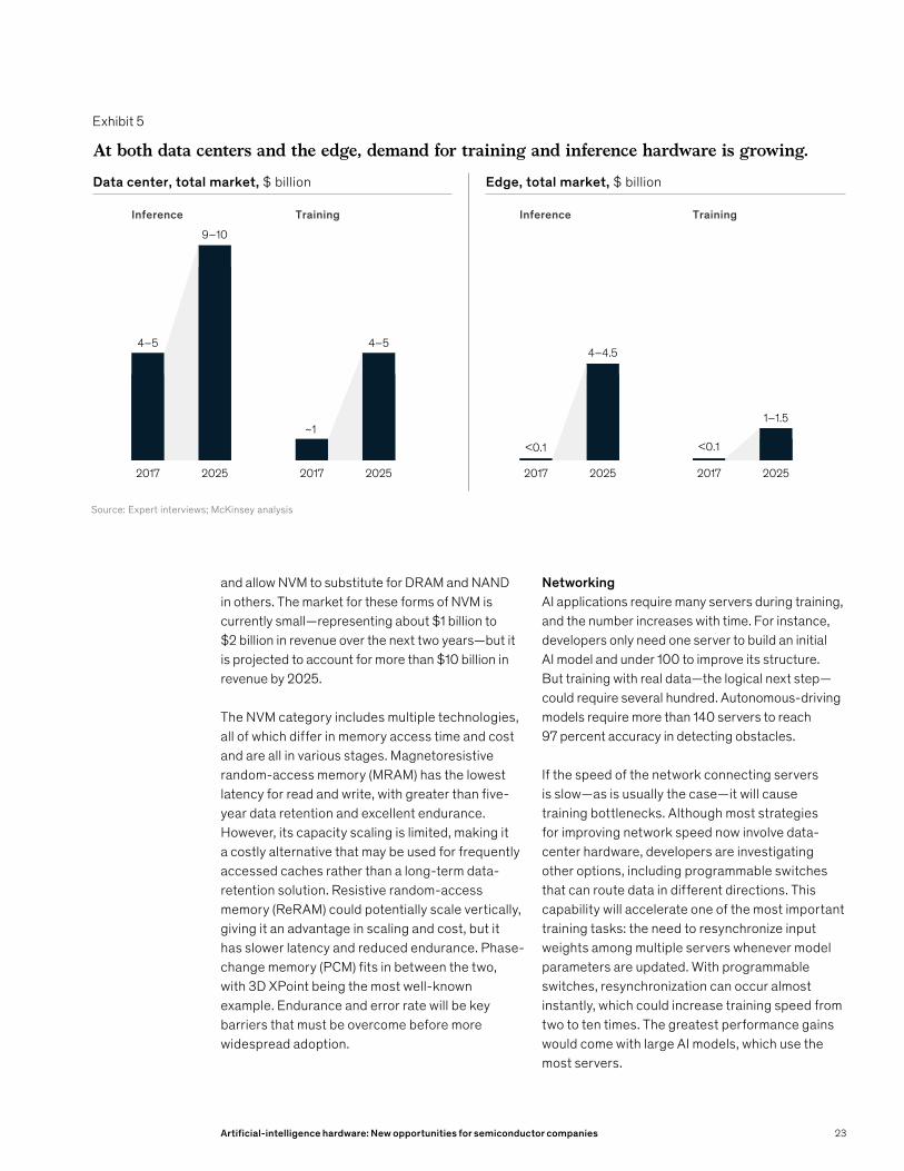
NetworkingAI applications require many servers during training, and the number increases with time. For instance, developers only need one server to build an initial AI model and under 100 to improve its structure. But training with real data—the logical next step—could require several hundred. Autonomous-driving models require more than 140 servers to reach 97 percent accuracy in detecting obstacles.
If the speed of the network connecting servers is slow—as is usually the case—it will cause training bottlenecks. Although most strategies for improving network speed now involve data-center hardware, developers are investigating other options, including programmable switches that can route data in different directions. This capability will accelerate one of the most important training tasks: the need to resynchronize input weights among multiple servers whenever model parameters are updated. With programmable switches, resynchronization can occur almost instantly, which could increase training speed from two to ten times. The greatest performance gains would come with large AI models, which use the most servers.
Exhibit 5
McKinsey on Semiconductors 2018Artificial intelligence semiconductorsExhibit 5 of 6
At both data centers and the edge, demand for training and inference hardware is growing.
Data center, total market, $ billion Edge, total market, $ billion
Source: Expert interviews; McKinsey analysis
Inference Training
2017
4–5 4–5
~1
9–10
2025 2017 2025
Inference Training
4–4.5
1–1.5
<0.1 <0.1
2017 2025 2017 2025
23

Another option to improve networking involves using high-speed interconnections in servers. This technology can produce a threefold improvement in performance, but it’s also about 35 percent more expensive.
Semiconductor companies need new strategies for the AI marketIt’s clear that opportunities abound, but success isn’t guaranteed for semiconductor players. To capture the value they deserve, they’ll need to focus on end-to-end solutions for specific industries (also called microvertical solutions), ecosystem development, and innovation that goes far beyond improving compute, memory, and networking technologies.
Customers will value end-to-end solutions for microverticals that deliver a strong return on investmentAI hardware solutions are only useful if they’re compatible with all other layers of the technology stack, including the solutions and use cases in the services layer. Semiconductor companies can take two paths to achieve this goal, and a few have already begun doing so. First, they could work with partners to develop AI hardware for industry-specific use cases, such as oil and gas exploration, to create an end-to-end solution. For example, Mythic has developed an ASIC to support edge inference for image- and voice-recognition
applications within the healthcare and military industries. Alternatively, semiconductor companies could focus on developing AI hardware that enables broad, cross-industry solutions, as Nvidia does with GPUs.
The path taken will vary by segment. With memory and storage players, solutions tend to have the same technology requirements across microverticals. In compute, by contrast, AI algorithm requirements may vary significantly. An edge accelerator in an autonomous car must process much different data from a language-translation application that relies on the cloud. Under these circumstances, companies cannot rely on other players to build other layers of the stack that will be compatible with their hardware.
Active participation in ecosystems is vital for successSemiconductor players will need to create an ecosystem of software developers that prefer their hardware by offering products with wide appeal. In return, they’ll have more influence over design choices. For instance, developers who prefer a certain hardware will use that as a starting point when building their applications. They’ll then look for other components that are compatible with it.
To help draw software developers into their ecosystem, semiconductor companies should reduce complexity whenever possible. Since
How we estimated value
We took a bottom-up approach to estimate the value at stake for semiconductor companies. Consider accelerators used for compute functions. First, we determined the percent of servers in data centers that were used
for artificial intelligence (AI). We then identified the type of logic device they commonly used and the average sales price for related accelerators. For edge computing, we conducted a similar review, but we focused on determining
the number of devices that were used for AI, rather than servers. By combining our insights for data centers and edge devices, we could estimate the potential value for semiconductor companies related to compute functions.
24 McKinsey on Semiconductors Number 7, October 2019

Artificial-intelligence hardware: New opportunities for semiconductor companies
there are now more types of AI hardware than ever, including new accelerators, players should offer simple interfaces and software-platform capabilities. For instance, Nvidia provides developers with Compute Unified Device Architecture, a parallel-computing platform and application programming interface (API) that works with multiple programming languages. It allows software developers to use Compute Unified Device Architecture–enabled GPUs for general-purpose processing. Nvidia also provides software developers with access to a collection of primitives for use in DL applications. The platform has now been deployed across thousands of applications.
Within strategically important industry sectors, Nvidia also offers customized software-development kits. To assist with the development of software for self-driving cars, for instance, Nvidia created DriveWorks, a kit with ready-to-use software tools, including
object-detection libraries that can help applications interpret data from cameras and sensors in self-driving cars.
As preference for certain hardware architectures builds throughout the developer community, semiconductor companies will see their visibility soar, resulting in better brand recognition. They’ll also see higher adoption rates and greater customer loyalty, resulting in lasting value.
Only platforms that add real value to end users will be able to compete against comprehensive offerings from large high-tech players, such as Google’s TensorFlow, an open-source library of ML and DL models and algorithms.⁴ TensorFlow supports Google’s core products, such as Google Translate, and also helps the company solidify its position within the AI technology stack, since TensorFlow is compatible with multiple compute accelerators.
4 An open-source, machine-learning framework for everyone, available at tensorflow.org.
Exhibit 6
McKinsey on Semiconductors 2018Artificial intelligence semiconductorsExhibit 6 of 6
The preferred architectures for compute are shifting in data centers and the edge.
Data-center architecture, % Edge architecture, %
¹ Application-speci�c integrated circuit. ² Central processing unit. ³ Field programmable gate array. ⁴ Graphics-processing unit. Source: Expert interviews; McKinsey analysis
ASIC1 CPU2 FPGA3 GPU4 Other
Inference Training
2017 2025 2017 2025
75
10
10 10
40
15
50
97
40
50
Inference Training
2017 2025 2017 2025
50
60
20 2030
70
50
70
10 10 10
25

Innovation is paramount, and players must go up the stackMany hardware companies that want to enable AI innovation focus on improving the computation process. Traditionally, this strategy has involved offering optimized compute accelerators or streamlining paths between compute and data through innovations in memory, storage, and networking. But hardware companies should go beyond these steps and seek other forms of innovation by going up the stack. For example, AI-based facial-recognition systems for secure authentication on smartphones were enabled by specialized software and a 3-D sensor that projects thousands of invisible dots to capture a geometric map of a user’s face. Because these dots are much easier to process than several millions of pixels from cameras, these authentication systems work in a fraction of a second and don’t interfere with the user experience. Hardware companies could also think about how sensors or other innovative technologies can enable emerging AI use cases.
Semiconductor companies must define their AI strategy nowSemiconductor companies that take the lead in AI will be more likely to attract and retain customers and ecosystem partners—and that could prevent later entrants from attaining a leading position in the market. With both major technology players and start-ups launching independent efforts in the AI hardware space now, the window of opportunity for staking a claim will rapidly shrink over the next few years. To establish a strong strategy now, they should focus on three questions:
— Where to play? The first step to creating a focused strategy involves identifying the target industry microverticals and AI use cases. At the most basic level, this involves estimating the size of the opportunity within different verticals, as well as the particular pain points that AI
solutions could eliminate. On the technical side, companies should decide if they want to focus on hardware for data centers or the edge.
— How to play? When bringing a new solution to market, semiconductor companies should adopt a partnership mind-set, since they might gain a competitive edge by collaborating with established companies within specific industries. They should also determine what organizational structure will work best for their business. In some cases, they might want to create groups that focus on certain functions, such as R&D, for all industries. Alternatively, they could dedicate groups to select microverticals, allowing them to develop specialized expertise.
— When to play? Many companies might be tempted to jump into the AI market, since the cost of being a follower is high, particularly with DL applications. Further, barriers to entry will rise as industries adopt specific AI standards and expect all players to adhere to them. While rapid entry might be the best approach for some companies, others might want to take a more measured approach that involves slowly increasing their investment in select microverticals over time.
The AI and DL revolution gives the semiconductor industry the greatest opportunity to generate value that it has had in decades. Hardware can be the differentiator that determines whether leading-edge applications reach the market and grab attention. As AI advances, hardware requirements will shift for compute, memory, storage, and networking—and that will translate into different demand patterns. The best semiconductor companies will understand these trends and pursue innovations that help take AI hardware to a new level. In addition to benefiting their bottom line, they’ll also be a driving force behind the AI applications transforming our world.
Copyright © 2019 McKinsey & Company. All rights reserved.
Gaurav Batra is a partner in McKinsey’s Washington, DC, office; Zach Jacobson and Andrea Queirolo are associate partners in the New York office; Siddarth Madhav is a partner in the Chicago office; and Nick Santhanam is a senior partner in the Silicon Valley office.
The authors wish to thank Sanchi Gupte, Jo Kakarwada, Teddy Lee, and Ben Byungchol Yoon for their contributions to this article.
26 McKinsey on Semiconductors Number 7, October 2019

Blockchain 2.0: What’s in store for the two ends—semiconductors (suppliers) and industrials (consumers)?
Blockchain 2.0: What’s in store for the two ends—semiconductors (suppliers) and industrials (consumers)?Ten years after blockchain’s inception, it is presenting new opportunities for both suppliers, such as semiconductor companies, and consumers, such as industrials.
© Imaginima/Getty Images
by Gaurav Batra, Rémy Olson, Shilpi Pathak, Nick Santhanam, and Harish Soundararajan
27

Blockchain is best known as a sophisticated and somewhat mysterious technology that allows cryptocurrencies to change hands online without assistance from banks or other intermediaries. But in recent years, it has also been promoted as the solution to business issues ranging from fraud management to supply-chain monitoring to identity verification. Despite the hype, however, block-chain’s use in business is still largely theoretical. A few pioneers in retail and other sectors are exploring blockchain business applications related to supply-chain management and other processes, but most are reluctant to proceed further because of high costs, unclear returns, and technical difficulties.
But we may now be at a transition point between Blockchain 1.0 and Blockchain 2.0. In the new era, blockchain-enabled cryptocurrency applications will likely cede their prominence to blockchain business applications that can potentially increase efficiency and reduce costs. These applications will be in a good position to gain steam, since many large tech companies may soon begin offering blockchain as a service (BaaS). Rather than just providing the hardware layer, as they’ve traditionally done, these companies will extend their services up the technology stack to blockchain platforms and tools. As blockchain deployment becomes less complex and expensive, companies that have sat on the sidelines may now be willing to take the plunge. (See sidebar, “What advantages do blockchain business applications offer?”)
Will blockchain business applications continue to grow and finally validate their promise? Industrial companies, which were largely on the sidelines during the Blockchain 1.0 era, want an answer to this question because they could find opportunities to deploy business applications that improve their bottom line. Semiconductor companies are also interested in the growth of both blockchain business applications and blockchain-enabled cryptocurrency because this could increase demand for chips.
Both industrial and semiconductor players will need a solid understanding of specific blockchain-enabled use cases and the market landscape to succeed in the new era. To assist them, this article reviews the changing market and then focuses on
specific strategies for capturing value. One caveat: all information in this article reflects data available as of December 2018. Cryptocurrency values fluctuate widely, so the numbers reported, including those for market capitalization, may not reflect the most recent data. Blockchain technology and the competitive landscape are also evolving rapidly, and there may have been changes since publication.
Blockchain 1.0: The cryptocurrency eraIt is not surprising that many people conflate blockchain with Bitcoin, the first and most dominant cryptocurrency. Until recently, the vast majority of blockchain applications involved enabling cryptocurrency transactions. Around 2014, however, private companies began investigating the use of blockchain for other business applications. Since most of these players are still at the pilot stage, it is fair to say that blockchain-enabled cryptocurrency has been the focus of the Blockchain 1.0 era.
The emergence of cryptocurrenciesBitcoin hit the market in 2009 as an open-source software application. It was first used in a commer-cial transaction in 2010, when two pizzas were bought for 10,000 bitcoin (under $10 then, but about $35 million as of December 2018). With no central authority or server to verify transactions, the public was initially skeptical about Bitcoin and reluctant to use it. Beginning in 2014, however, Bitcoin experienced a meteoric increase in user base, brand-name recognition, and transaction volume. Its value is extremely volatile, however, and it has declined sharply from its late 2017 peak of more than $19,000.
The past two years have seen the most growth in blockchain-enabled cryptocurrencies, with the number increasing from 69 in 2016 to more than 1,500 in 2018. Even though Bitcoin’s value has decreased this year, an influx of initial coin offerings (ICOs) has increased the market capitalization for cryptocurrencies (Exhibit 1).
Many of the additional currencies—also called “alt-coins”—were created to address certain gaps or inefficiencies with Bitcoin, and they are available through various networks. Popular altcoins
28 McKinsey on Semiconductors Number 7, October 2019

include Dash, Litecoin, and XRP (offered through Ripple). Of all the alternative cryptocurrency networks, Ethereum is most popular. It is an open-source platform that allows users to build and launch decentralized applications, including cryptocurrencies or digital ledgers. Users must spend a specific digital currency, Ether, to run applications on Ethereum. Ether can also serve as an alternative to regular money, but its primary purpose is to facilitate Ethereum operations.
Together, the market capitalization of a select set of major cryptocurrencies was about $150 billion in December 2018, with Bitcoin and the four leading altcoins representing about 75 percent of this value. Bitcoin’s market capitalization of about $60 billion was the highest.
Transaction verificationThe method used to verify transactions varies by cryptocurrency. With Bitcoin, the first participant, or “miner,” to validate a transaction and add a new block of data to the digital ledger will receive a certain number of tokens as a reward. Under this model, which is referred to as a proof-of-work (PoW) system, miners have an incentive to act quickly. But validating a transaction doesn’t simply involve verifying that Bitcoin has been transferred from one account to another. Instead, a miner has to answer a cryptographic question by correctly identifying an alphanumeric series associated with the transaction. This activity requires a lot of trial and error, making the hash rate—the compute speed at which an operation is completed—extremely important with Bitcoin.
Exhibit 1
McKinsey on Semiconductors 2018Blockchain 2.0Exhibit 1 of 3
The number of active cryptocurrencies and their market capitalization has soared.
Cryptocurrencies active in the market, number Cryptocurrency market capitalization,¹ $ billion
¹ This is the market capitalization for a select bundle of cryptocurrencies. Bundle includes: Bitcoin, Dash, Ethereum, Litecoin, Ripple, and several other altcoins. Figures are as of Dec 11, 2018.
2013
8 29 3369
392
1,500+
2018
27 4
11
177
~150
2013 2018
Blockchain 2.0: What’s in store for the two ends—semiconductors (suppliers) and industrials (consumers)? 29

In the beginning, many individuals mined Bitcoin as a hobby. But as interest in cryptocurrencies grew, the number and size of Bitcoin miners soared, necessitating more sophisticated hardware and more intense computing power. This shift has favored the rise of large mining pools. Many of these, including AntPool and BTC.COM, are based in China. The top five mining pools account for 70 to 85 percent of the overall Bitcoin network’s collective hash rate, or computing power.
Hardware for cryptocurrency playersIn the early day of cryptocurrency, amateur hobbyists relied on central processing units (CPUs) to optimize compute performance. When the Bitcoin network began expanding around 2010, the graphics-processing unit (GPU) replaced the CPU as the accelerator of choice. The ascent of GPUs was short lived, however, since many companies began designing application-specific integrated circuits (ASICs) for cryptocurrency mining to improve hash rates.
About 50 to 60 percent of companies that manufacture ASICs for Bitcoin transactions are based in the Greater China region (Exhibit 2). (Some of these began creating ASICs for cryptocurrency mining before Bitcoin entered the market in 2008, since this was already viewed as a potential growth area.) BitMain Technologies, a China-based company, supplied 70 to 80 percent of the cryptocurrency ASICs in 2017. Its customers typically use “crypto rigs”—multiple ASICs working together—to optimize compute speed. By conservative estimates, BitMain Technologies has a gross margin of 65 to 75 percent and an operating margin of 55 to 65 percent—equivalent to $3 billion to $4 billion in 2017. That figure is roughly the same as the profit margin for Nvidia, which has been in business for 20 years longer.
Although most major cryptocurrencies now reward miners with high compute speed, some have taken steps to prevent large mining pools with crypto rigs from dominating the market. For instance, Ethash, the hashing algorithm that Ethereum uses, is designed
to be ASIC resistant—and that means miners must fetch random data and compute randomly selected transactions to solve their cryptographic questions. Both activities require frequent access to memory, which ASICs alone won’t provide. Ethereum miners primarily rely on a system that utilizes a GPU in combination with memory.
Blockchain 2.0: Uncertainty about cryptocurrencies and the emergence of business applicationsThe Blockchain 2.0 era will likely usher in many changes. The cryptocurrency market could become more diverse if Bitcoin continues to decrease in price, since ICOs may see the situation as an opportunity to stake their claims. Consumers may also begin demonstrating more interest in other established altcoins. For instance, users may come to favor Dash or Litecoin for some transactions, since they offer faster transaction speed than Bitcoin does. Companies and the general public are generally becoming more comfortable with cryptocurrency transactions, which could increase usage rates.¹
In tandem with these changes, the market for blockchain business applications is heating up as BaaS simplifies implementation. Demand for these applications is expected to be strong, and corporate users could soon outnumber cryptocurrency miners.
Investors are showing continued interest in blockchain, although funding levels have recently declined. Venture-capital funding peaked in 2017 at about $900 million for both cryptocurrency and business applications, and it will likely still be between $600 million and $800 million in 2018. It is unclear whether 2019 will show continued decline, a plateau, or greater investment.
Although it is difficult to make predictions about blockchain, since it is a relatively new technology, we were able to identify several trends in the cryptocurrency and business-application markets
1 Josh Ong, “The branding of cryptocurrency,” Forbes, March 1, 2018, forbes.com.
30 McKinsey on Semiconductors Number 7, October 2019

that could affect demand for this technology. Here is what we found.
The cryptocurrency market is evolving rapidly, but uncertainties remainDespite the widespread press attention that cryptocurrencies receive, their practical value is still limited. Most people regard them as something of an online Swiss bank account—a haven for activities that can’t be closely tracked by authorities. In many cases, potential users hold back because they don’t believe cryptocurrencies are secure. Digital-ledger technology, the backbone of blockchain, has never been hacked, but cryptocurrencies are vulnerable in other ways. The most infamous theft occurred in 2014 when someone took 850,000 bitcoin from the Mt. Gox exchange by assuming another person’s identity. In the corporate sphere, only about 3,000 companies now accept Bitcoin transactions.
Future growth of cryptocurrenciesIt is difficult to predict whether cryptocurrencies will experience strong growth in Blockchain 2.0, since corporate leaders and members of the public
may have lingering doubts that are difficult to overcome. But we do expect to see greater usage rates. In addition, miners will have a greater number of options from which to choose. Although Bitcoin now represents about 40 to 50 percent of market capitalization for cryptocurrency, other altcoins are becoming more popular. Ethereum, for instance, now accounts for more than 10 percent of the market capitalization. And small ICOs—those beyond the top 20—now represent about 20 percent of market capitalization, up from 5 percent only two years ago.
Government intervention—particularly the development of laws and regulations—may strongly influence the cryptocurrency market over the next few years. If the current market provides any clues, it is unlikely that a global consensus will emerge. For instance, some governments allow individuals to use cryptocurrency but prohibit banks and securities companies from doing so. Other countries take a much stricter approach by forbidding ICOs to operate within their borders. If additional governments adopt this stance, cryptocurrency uptake could be limited.
Exhibit 2
McKinsey on Semiconductors 2018Blockchain 2.0Exhibit 2 of 3
Many companies have designed application-speci�c integrated chips to mine cryptocurrencies.
A timeline of cryptocurrency chip manufacturers
Note: Gh = gigahash; J = joule; sec = second; Th = terahash; W = watt.
2006 2007 2008 2009 2010 2011 2012 2013 2014 2015 2016 2017 2018
CompanyHQRecent productLaunchHash ratePower e�ciency
CompanyHQRecent productLaunchHash ratePower e�ciency
Canaan CreativeBeijing, ChinaAvalonMiner 851Aug 201815 Th/sec0.11 J/Gh
Halong MiningNot applicable (online only)Dragonmint T16Mar 201816 Th/sec 0.075 J/Gh
CoinBau GmbHDresden, GermanyWolfCAVE XENot available4.8 Th/sec0.27 W/Gh
Butter�y LabsLeawood, KS, USMonarch Aug 2014725 or 825 Gh/sec0.7 W/Gh
BitMain TechnologiesBeijing, ChinaAntminer S9-HydroAug 201818 Th/sec0.096 J/Gh
BitfuryDC, USBitfury TardisOct 201880 Th/sec0.055 J/Gh
INNOSILICON Technology Ningbo, ChinaT2 Turbo+ 32T Sept 201832 Th/sec0.069 J/Gh
CoinTerraCA, USTerraMiner IVJan 20141.6 Th/sec0.6 W/Gh
Black ArrowGuangdong, ChinaProspero X36Dec 20152.2 Th/sec0.7 W/Gh
Ebang CommunicationHangzhou, ChinaEBIT E11+Oct 201837 Th/sec0.055 J/Gh
Blockchain 2.0: What’s in store for the two ends—semiconductors (suppliers) and industrials (consumers)? 31

Another big question relates to investment. Funding for ICOs usually comes from venture capitalists because pension funds and other institutional investors consider cryptocurrency too risky. (The majority of ICOs do not yet have customers nor do they generate revenue.) Even though venture-capital investment in cryptocurrency has increased, the lack of interest from institutional investors could restrict future growth to some extent.
Changing algorithms Behind the scenes, more subtle changes are occurring in the cryptocurrency market as players try to minimize the importance of compute power by developing new algorithms. For instance, Ethereum is considering the replacement of its PoW system with one based on proof of stake (PoS). In a PoS system, participants are rewarded based on the number of coins they have in their digital wallets and the length of time they have had these stakes. The participant that rates highest on these factors is chosen to validate a transaction and receive a reward. Many other large cryptocurrency networks, including Cardano, Dash, and EOS, are also investigating PoS algorithms.
PoS systems have several advantages. First, they help cryptocurrency networks build a trusted network of loyal participants—and this may make security breaches less common. Second, they level the playing field for cryptocurrency miners, since those with the greatest compute power will not necessarily be the winners. Players also appreciate that PoS systems are more energy efficient and allow faster transactions. A shift to PoS systems could have major implications for semiconductor companies that serve cryptocurrency players, since it would shift chip demand in new directions.
A new look at business applications, but with doubts about scalabilityRecent McKinsey research has identified more than 90 use cases for blockchain business applications across industries. Many near-term use cases will involve applying blockchain to reduce costs associated with existing processes, such as the exchange of medical records among providers, insurers, researchers, and patients. In these activities, blockchain can remove the need for
intermediaries and decrease administrative costs associated with record keeping. Over the longer term, blockchain might be used to improve fraud management, supply-chain monitoring, cross-border payments, identity verification, and the protection of copyrights or intellectual property. It could also help companies with smart contracts—transactions that execute automatically when certain conditions are met.
Many companies and organizations are now supporting the development of blockchain business applications. The Linux Foundation has created Hyperledger, an open-source collaborative effort to develop blockchain technologies for multiple industries. Similarly, the company R3 leads a large consortium that developed Corda, a blockchain platform for use in financial services and commerce. Corporate investment in blockchain hit $1 billion in 2017 and is expected to grow at a compound annual growth rate of 50 percent through 2021.
Despite these efforts, blockchain business applications arguably remain stuck at the pilot stage, with most companies still attempting to demonstrate proof of concept (PoC). (The greatest wave of business applications undergoing PoC occurred from 2016 to 2017; the number at this stage is now smaller.) Many start-ups that offer business applications have failed to obtain Series C funding—the investment designed to promote growth and scale operations. The emergence of competing technologies is the major reason for the lack of progress. For instance, with payments, financial institutions can now use a messaging network that allows for greater transaction speeds and more transparency than past methods. This technology reduces the need for blockchain-based solutions and discourages incumbents in the financial sector from investing in blockchain.
Much interest in blockchain business applications stems from the recent advent of BaaS, which simplifies the creation of the complex, five-layer blockchain technology stack (Exhibit 3). Until the past year, enterprise customers had to build individual layers themselves or cobble them together from disparate sources. Among other tasks, they had to customize existing digital-ledger fabric platforms
32 McKinsey on Semiconductors Number 7, October 2019

(distributed computing platforms with a base protocol and configurable functions). They also had to acquire and integrate data, define permissions and governance protocols, and code software. Most enterprises simply lacked the funds or in-house technology talent to make this happen.
With the emergence of BaaS, the onus of deployment has moved from customers to providers. While BaaS is typically limited to the infrastructure layer, some providers also create tools that extend into the data and digital-ledger layers. With access to these offerings, customers can significantly reduce the deployment costs of a new blockchain system. For instance, they will no longer have to invest heavily in data or in ledger software and services to make their fabric platforms operational.
How industrial companies can create value in Blockchain 2.0: Core beliefs Across industries, companies have been exploring blockchain opportunities. Many consumer-facing and industrial companies were somewhat late to the game because most applications were geared toward cryptocurrency or financial transactions during Blockchain 1.0. But their involvement will increase as more blockchain business applications move from the concept stage to reality. For industrial companies, the potential use cases span all areas of their operations, and a few have already become reality:
— An industrial company formed a partnership with a technology business that uses blockchain to track the origin of goods and their progress along the supply chain. By providing greater transparency, the company helped customers understand the quality of its materials, the supply-chain process, and the sources of raw ingredients.
— A leading manufacturer of Internet of Things (IoT) devices formed a partnership with a blockchain start-up to create “digital passports” for individual IoT devices. The goal was to improve the expensive and time-consuming process for authentication, which involved obtaining physical certificates from authorities.
By registering a device on blockchain, the company could give it a unique digital identity that could not be altered. The company could easily update the digital identity in real time to reflect any changes—a service it could not perform with physical certificates.
To help blockchain applications gain traction at industrial companies, stakeholders must address four structural challenges: inertia that prevents players from collaborating, a lack of standards, unclear legal and regulatory frameworks, and latency issues that make it difficult to verify multiple transactions rapidly. For instance, Bitcoin is limited to seven transactions per second, and Ethereum can achieve 20 transactions per second. Financial institutions, such as credit-card companies, can handle between 24,000 and 56,000 transactions per second.
Based on our review of the industrial sector, we have identified three core beliefs about the ability of companies to create and capture value during Blockchain 2.0.
Belief 1: The value is in specific use cases that depend on incorruptible record keepingBlockchain’s value proposition is clear: it functions as a decentralized, incorruptible database that allows peers to conduct transactions without relinquishing control to an intermediary or accepting counterparty risk. For industrial companies, such incorruptible record keeping (IRK) can be invaluable. For instance, a global wireless-network-equipment company used blockchain to provide cybersecurity for various industrial companies that used IoT, including those in utilities, oil and gas, and transportation. The IoT devices had tens of thousands of nodes, each of which represented a potential entry point for hackers. With blockchain, the company could track security threats by assigning each node a unique key that allowed it to detect unusual behavior or hacker intrusions immediately. In those cases for which IRK is not essential, industrial companies should consider using a traditional shared database for transactions, since it is less expensive to maintain.
Blockchain 2.0: What’s in store for the two ends—semiconductors (suppliers) and industrials (consumers)? 33

Belief 2: Scalable use cases will involve high value, low volume, and collaborative mechanisms The list of potential blockchain applications that industrial companies could implement is long. They could facilitate smart contracts, provide customers with a clear record of a product’s origin, enhance logistics and supply chain, improve product quality, or help satisfy regulatory requirements. But not every industrial use case with strong potential will survive past the PoC stage. Those that are most likely to gain traction share three characteristics:
— High value. Each blockchain application must deliver significant value to the bottom line. If an information breach could cause a company to lose millions of dollars, a blockchain application might be infinitely
preferable to a traditional shared database, for instance. Similarly, blockchain applications that significantly reduce cost by increasing efficiency are well worth exploring. For instance, a machinery manufacturer may have a supply chain that involves multiple intermediaries. A blockchain application that could reduce cost and complexity during shipping would deliver enormous value.
— Low transaction volume. Blockchain technology still has limited processing power, which makes it difficult to perform many transactions simultaneously. Until the technology advances, industrial companies should apply it to use cases that involve limited transaction volume. For instance, a consumer-
Exhibit 3
McKinsey on Semiconductors 2018Blockchain 2.0Exhibit 3 of 3
The blockchain technology stack includes ve layers.
Technology layer Core function
Source: Asian Venture Capital Journal; VCCEdge; McKinsey analysis
Development platform and infrastructure
Digital-ledger fabricplatform
Data
Digital-ledger softwareand services
Applications
Enable user interface and implement business logic (ie, portion of an enterprise system that determines how data are transformed or calculated, and how they are routed to people or software)
Are typically domain or industry speci�c
Ensure interoperability of systems and manage permissions, disaster recovery, and governance
Contain ecosystem of data, such as sales information and shipping records, pulled into blockchain application
Provide base protocol and con�gurable functionalities for various services, such as smart contracting
Provide infrastructure for hosting and developing blockchain, and for operating nodes
Include hardware
34 McKinsey on Semiconductors Number 7, October 2019

equipment manufacturer could use blockchain to track and manage a few SKUs for select end consumers, rather than its entire customer base.
— Market mechanisms for ensuring collaboration. Several blockchain use cases, such as those for tracking goods through supply chains, will require players to share data and participate in a common blockchain platform. Initially, few companies may be willing to engage in such collaborations. In some specific cases where companies have the market power, either because of their size or position, they will be more likely to have other players participate and obtain value from blockchain solutions.
By concentrating on use cases with these characteristics, industrial companies will prioritize those that are most likely to provide a suitable return on investment. As blockchain technology progresses and the cost of application development falls, they may investigate additional use cases.
Belief 3: Blockchain 2.0 will take off in private, permissioned networks within the industrial ecosystem Unlike cryptocurrency transactions, industrial business applications will occur over private blockchains that limit access to invited participants, rather than over public blockchains. Some of these blockchains will have central administrators to determine which nodes have permission to access, edit, and validate data. Along with providing greater confidentiality, these private, permissioned networks are the most technically feasible, given that blockchain speed decreases and latency increases as more nodes are added.
For industrial companies, the first private, permissioned blockchains will focus on specific
“microverticals”—groups of related tasks—such as supply-chain management. Within such micro-verticals, participants are more likely to identify a common problem that they want to solve through blockchain and recognize the return on investment. They are also more willing to share implementation costs, since they can easily see blockchain’s value. For example, leaders at industrial companies and the vendors that serve them will all benefit if they
can optimize a process, reduce costs, and improve efficiency. These companies will be the most willing to participate in private, permissioned networks in order to restrict access to sensitive information, such as pricing data, to select groups or individuals.
BaaS providers typically offer their platforms for free and then charge customers for each node deployed. This pricing strategy could help industrial players, since companies generally deploy few nodes during early implementation. Since industrial companies’ financial risks are lower, they may be enticed to embark on more blockchain projects, even though they are uncertain about the potential returns.
How semiconductor players can create value in Blockchain 2.0: Core beliefs Semiconductor companies have found many opportunities in blockchain since its inception. That will still be the case in the Blockchain 2.0 era, but we anticipate some important changes as the cryptocurrency sector evolves and business applications potentially become the primary sources of chip demand. So, what trends must semiconductor players understand to succeed? And who will win in this new era, for both cryptocurrency and blockchain business applications? After analyzing the hardware market, we identified four beliefs about value creation and capture by silicon companies during Blockchain 2.0.
Belief 1: Value for silicon players will migrate away from cryptocurrencies (and therefore compute power) in the near futureUntil blockchain business applications gain traction and demonstrate a positive return on investment—something that is not expected to occur for at least two to three years—semiconductor companies should continue to focus on cryptocurrency customers. In particular, they should try to optimize compute power and minimize power consumption to satisfy the large mining pools that rely on crypto rigs. Recently, BitMain Technologies made an important advance in this area by developing a seven-nanometer node miner.
A long-term focus on compute power isn’t the best strategy, however, since many altcoins are considering moving from PoW to PoS systems,
Blockchain 2.0: What’s in store for the two ends—semiconductors (suppliers) and industrials (consumers)? 35

in which compute power is less important. For blockchain business applications, which could represent the wave of the future, compute power is essential but not a differentiator. Instead, semiconductor companies and other players will win by enabling or providing BaaS.
Belief 2: To win in Blockchain 2.0, semiconductor companies can’t just understand their customers—they also have to understand their customers’ customers Cryptocurrency ASICs have been in extremely high demand since 2016, because miners began getting higher rewards for adding the next block. Most orders come from the top five Bitcoin mining pools in China, and the demand could increase over the next few years. This trend will keep orders flowing into substrates, ASIC designers, foundries, outsourced assembly and testing companies, and equipment manufacturers.
With value migrating from cryptocurrencies to blockchain business applications, and with BaaS players gaining market share, semiconductor
companies will need to develop new strategies that align with their customers’ priorities. To do so effectively, they must ask themselves four questions:
— In which specific use cases and microverticals are customers likely to adopt a blockchain solution at scale?
— Which customers or end markets have the market position and structure to ensure that all relevant companies will be willing to collaborate?
— How do end customers plan to use blockchain and what aspects of our hardware—for instance, cost, compute capability, or power consumption—will differentiate the winners from the losers?
— How can we work with (or without) BaaS players, including those who provide other hardware components, software integration, or go-to-market capabilities, to enable end-to-end solutions for customers?
What advantages do blockchain business applications offer?
Think of blockchain as a database shared across a number of participants, each with a computer. At any moment, each member of the blockchain holds an identical copy of the blockchain database, giving all participants access to the same information. All blockchains share three characteristics:
— A cryptographically secure database. When data are read or written, users must provide the correct cryptographic keys—one public (essentially, the address) and one private. Users cannot update the blockchain unless they have the correct keys.
— A digital log of transactions. Transactional information is available
in real time through the blockchain network. Companies doing business with each other must thus store most of their transactional information in digital form to take advantage of blockchain.
— A public or private network that enables sharing. Anyone can join or leave a public network without express permission. Admission into private networks is by invitation only.
Blockchain’s cryptographic keys provide leading-edge security that goes far beyond that found in a standard distributed ledger. The technology also eliminates the possibility that a single point of failure will emerge since the blockchain database is distributed and decentralized. If one node
fails, the information will still be available elsewhere. Another advantage involves the audit trail. Users can go back through the blocks of information and easily see the information previously recorded in the database, such as the previous owner of a piece of property. And perhaps most important, blockchain maintains process integrity. The database can only be updated when two things happen. First, a user must provide the correct public and private keys. Second, a majority of participants in the network must verify those credentials. This reduces the risk that a malicious user will gain illicit access to the network and make unauthorized updates.
36 McKinsey on Semiconductors Number 7, October 2019

Belief 3: As value migrates away from hardware, semiconductor companies must go ‘up the stack’ Within the current BaaS technology stack, value predominantly lies within the lowest layer: hardware. But over the next several years, as blockchain business applications start to gain a foothold within large industries, demand will increase for hardware customized for specific use cases or microverticals. This development will cause value to migrate up the technology stack from hardware to other layers.
Given these trends, semiconductor companies should consider enabling or providing the entire BaaS technology stack for specific microverticals or use cases. After developing a clear understanding of how customers plan to use their blockchain chips, semiconductor companies could then provide platforms and plug-ins that help integrate the layers of the blockchain technology stack, allowing for easier implementation. A combined offering would meet all customer needs for blockchain, just as TensorFlow does for machine learning and deep learning.
This strategy will become even more important as the use cases and microverticals start to mature, since hardware will become a commodity. Those semiconductor providers that don’t move “up the stack” will have an increasingly difficult time capturing value and thriving. In fact, they could find themselves in the same situation they face in the data-center market, where “hyperscalers” have a great deal of control because of their purchasing power.
Belief 4: The semiconductor companies that were leaders in Blockchain 1.0 are not preordained to be future winnersToday’s top blockchain hardware providers, including BitMain Technologies, Canaan Creative,
and Ebang Communication, are now in strong positions. But they might not be the long-term winners, despite their first-mover advantage. The barriers to market entry are low, since new companies with domain expertise can easily design ASICs, and some well-known companies are already planning to move into the market.
If the new players can differentiate themselves based on product performance or price, they may dethrone the current market leaders. Companies with strong end-to-end BaaS offerings may lead the pack, while those that continue to focus on hardware alone may find themselves sidelined.
If blockchain were a tool, it would be a Swiss Army knife that has a blade, a screwdriver, a can opener, and many other attachments—a clever technology that enables a diverse set of use cases that go far beyond cryptocurrency. But like a Swiss Army knife, blockchain can be unexpectedly complicated. Industrial companies must know what networks and transactions are most likely to benefit their business. They must also understand which use cases have features that are most likely to deliver value at scale—for instance, characteristics that encourage other participants to join the blockchain and collaborate. Likewise, semiconductor companies must understand how blockchain is being applied in the cryptocurrency market and the business sphere and closely follow market developments in both areas. With blockchain evolving so rapidly, it can be difficult to keep pace with change. But those semiconductor companies and industrials that pursue innovation while aggressively enabling blockchain use cases are likely to reap the greatest rewards.
Copyright © 2019 McKinsey & Company. All rights reserved.
Gaurav Batra is a partner in McKinsey’s Washington, DC, office; Rémy Olson is an alumnus of the San Francisco office; Shilpi Pathak is an alumnus of in the Chicago office; Nick Santhanam is a senior partner in the Silicon Valley office; and Harish Soundararajan is an alumnus of the Boston office.
The authors wish to thank Jo Kakarwada and Celine Shan for their contributions to this article.
Blockchain 2.0: What’s in store for the two ends—semiconductors (suppliers) and industrials (consumers)? 37

Rethinking car software and electronics architectureAs the car continues its transition from a hardware-driven machine to a software-driven electronics device, the auto industry’s competitive rules are being rewritten.
© Just_Super/Getty Images
by Ondrej Burkacky, Johannes Deichmann, Georg Doll, and Christian Knochenhauer
38 McKinsey on Semiconductors Number 7, October 2019

Rethinking car software and electronics architecture
The engine was the technology and engineering core of the 20th-century automobile. Today, software, large computing power, and advanced sensors have increasingly stepped into that role; they enable most modern innovations, from efficiency to connectivity to autonomous driving to electrification and new mobility solutions.
However, as the importance of electronics and software has grown, so has complexity. Take the exploding number of software lines of code (SLOC) contained in modern cars as an example. In 2010, some vehicles had about ten million SLOC; by 2016, this expanded by a factor of 15, to roughly 150 million lines. Snowballing complexity is causing significant software-related quality issues, as evidenced by millions of recent vehicle recalls.
With cars positioned to offer increasing levels of autonomy, automotive players see the quality and security of vehicle software and electronics as key requirements to guarantee safety. This means the industry must rethink today’s approaches to vehicle software and electrical and electronic architecture.
Addressing an urgent industry concernAs the automotive industry transitions from hardware- to software-defined vehicles, the average software and electronics content per vehicle is rapidly increasing. Software represents 10 percent of overall vehicle content today for a D-segment (large) car (approximately $1,220), and the average share of software is expected to grow at a compound annual rate of 11 percent, to reach 30 percent of overall vehicle content (around $5,200) in 2030. Not surprisingly, companies across the digital automotive value chain are attempting to capitalize on inno-vations enabled through software and electronics (Exhibit 1). Software companies and other digital-technology companies are leaving their current tier-two and tier-three positions to engage automakers as tier-one suppliers. They’re expanding their participation in the automotive technology stack by moving beyond features and apps into operating systems. At the same time, traditional tier-one
electronic-system companies are boldly entering the tech giants’ original feature-and-app turf, and premium automakers are moving into areas further down the stack–such as operating systems, hardware abstractions, and signal processing– in order to protect the essence of their technical distinction and differentiation.
One consequence of these strategic moves is that the vehicle architecture will become a service-oriented architecture (SOA) based on generalized computing platforms. Developers will add new connectivity solutions, applications, artificial-intelligence elements, advanced analytics, and operating systems. The differentiation will not be in the traditional vehicle hardware anymore but in the user-interface and experience elements powered by software and advanced electronics.
Tomorrow’s cars will shift to a platform of new brand differentiators (Exhibit 2). These will likely include infotainment innovations, autonomous-driving capabilities, and intelligent safety features based on “fail operational” behaviors (for example, a system capable of completing its key function even if part of it fails). Software will move further down the digital stack to integrate with hardware in the form of smart sensors. Stacks will become horizontally integrated and gain new layers that transition the architecture into an SOA.
Ultimately, the new software and electronic architecture will come from several game-changing trends that drive complexity and interdependencies. For example, new smart sensors and applications will create a “data explosion” in the vehicle that companies need to handle by processing and analyzing the data efficiently, if they hope to remain competitive. A modularized SOA and over-the-air (OTA) updates will become key requirements to maintain complex software in fleets and enable new function-on-demand business models. Infotainment and, to a lesser degree, advanced driver-assistance systems (ADAS) will increasingly become “appified” as more third-party app developers provide vehicle content. Digital-security requirements will shift the focus from a pure access-control strategy to an
39

integrated-security concept designed to anticipate, avoid, detect, and defend against cyberattacks. The advent of highly automated driving (HAD) capabilities will require functionality convergence, superior computing power, and a high degree of integration.
Exploring ten hypotheses on future electrical or electronic architectureThe path forward for both the technology and the business model is far from fixed. But based on our extensive research and insights from experts, we developed ten hypotheses regarding tomorrow’s automotive electrical or electronic architecture and its implications for the industry.
There will be an increasing consolidation of electronic control units (ECUs) Instead of a multitude of specific ECUs for specific functionalities (the current “add a feature, add a box” model), the industry will move to a consolidated vehicle ECU architecture.
In the first step, most functionality will be centered on consolidated domain controllers for the main vehicle domains that will partially replace functionality currently running in distributed ECUs. These
developments are already under way and will hit the market in two to three years’ time. This consolidation is especially likely for stacks related to ADAS and HAD functionality, while more basic vehicle functions might keep a higher degree of decentralization.
In the evolution toward autonomous driving, virtualization of software functionality and abstraction from hardware will become even more imperative. This new approach could materialize in several forms. One scenario is a consolidation of hardware into stacks serving different requirements on latency and reliability, such as a high-performance stack supporting HAD and ADAS functionality and a separate, time-driven, low-latency stack for basic safety features. In another scenario, the ECU is replaced with one redundant “supercomputer,” while in a third, the control-unit concept is abandoned altogether in favor of a smart-node computing network.
The change is driven primarily by three factors: costs, new market entrants, and demand through HAD. Decreasing costs, both for the development of features as well as the required computing hardware, including communication hardware, will accelerate the consolidation. So too will new market
Exhibit 1
McKinsey Semiconductors 2019Rethinking car softwareExhibit 1 of 3
Software enables critical automotive innovations.Software innovation examples
Source: Automotive Electronics Initiative; Robert N. Charette, “This car runs on code,” IEEE Spectrum, February 2009, spectrum.ieee.org; HAWK; McKinsey analysis
• Integration of 3rd-party services • Updates over the air to deploy new features faster• Operation of future cars partly in the cloud
Connectivity
• Introduction of new electronics • Reduction of energy consumption through advanced software algorithms
Electrication
• Rise of built-in sensors and actuators• Higher demand for computing power and communication• Unlimited need for reliability
Autonomous driving
• Shared-mobility services and robo-taxis via app • Customized driver experience
Diverse mobility
Innovationthroughsoftware
40 McKinsey on Semiconductors Number 7, October 2019

Rethinking car software and electronics architecture
entrants into automotive that will likely disrupt the industry through a software-oriented approach to vehicle architecture. Increasing demand for HAD features and redundancy will also require a higher degree of consolidation of ECUs.
Several premium automakers and their suppliers are already active in ECU consolidation, making early moves to upgrade their electronic architecture, although no clear industry archetype has emerged at this point.
The industry will limit the number of stacks used with specific hardware Accompanying the consolidation will be a normalization of limited stacks that will enable a separation of vehicle functions and ECU hardware that includes increased virtualization. Hardware
and embedded firmware (including the operating system) will depend on key nonvehicle functional requirements instead of being allocated part of a vehicle functional domain. To allow for separation and a service-oriented architecture, the following four stacks could become the basis for upcoming generations of cars in five to ten years:
— Time-driven stack. In this domain, the controller is directly connected to a sensor or actuator while the systems have to support hard real-time requirements and low latency times; resource scheduling is time based. This stack includes systems that reach the highest Automotive Safety Integrity Level classes, such as the classical Automotive Open System Architecture (AUTOSAR) domain.
Exhibit 2
McKinsey Semiconductors 2019Rethinking car softwareExhibit 2 of 3
Architecture will become service oriented, with new factors for dierentiation.Future layered in-vehicle and back-end architecture
Future factors for brand dierentiation:
• Infotainment features requiring “plug and play” capabilities
• Autonomous capabilities including sensor-fusion algorithms as a complement to hardware
• Safety features based on “fail operational”² behavior
• Software will move further down stack to hardware (smart sensors)
• Stacks become horizontally integrated
• New layers will be added to stack
Cloud platformCombine in-vehicle data with environmental data
Existing layer
Signi�cant increase in number of applications
Analyze data for real-timedecisions and autonomous driving
Abstract applications from hardware
Closely controlled add-on app and modules due to safety considerations
Connectivity (back-haul)
User interface/user experience/ human–machine interface
Arti�cial intelligence/advanced analytics
Middleware layer/operating system
Electronic/electricalhardware1
Sensors ActuatorsPower
components
Vehicle
Applications
Modi�ed layer New layer
¹ Including operating system in status quo.² For example, a system capable of completing its key function even if part of it fails.
41

— Event- and time-driven stack. This hybrid stack combines high-performance safety applications, for example, by supporting ADAS and HAD capability. Applications and peripherals are separated by the operating system, while applications are scheduled on a time base. Inside an application, scheduling of resources can be based on time or priority. The operating environment ensures that safety-critical applications run on isolated containers with clear separation from other applications within the car. A current example is adaptive AUTOSAR.
— Event-driven stack. This stack centers on the infotainment system, which is not safety critical. The applications are clearly separated from the peripherals, and resources are scheduled using best-effort or event-based scheduling. The stack contains visible and highly used functions that allow the user to interact with the vehicle, such as Android, Automotive Grade Linux, GENIVI, and QNX.
— Cloud-based (off-board) stack. The final stack covers and coordinates access to car data and functions from outside the car. The stack is responsible for communication, as well as safety and security checks of applications (authentication), and it establishes a defined car interface, including remote diagnostics.
Automotive suppliers and technology players have already begun to specialize in some of these stacks. Notable examples are in infotainment (event-driven stack), where companies are developing communications capabilities such as 3-D and augmented navigation. A second example is artificial intelligence and sensing for high-performance applications, where suppliers are joining with key automakers to develop computing platforms.
In the time-driven domain, AUTOSAR and JASPAR are supporting the standardization of these stacks.
An expanded middleware layer will abstract applications from hardware As vehicles continue to evolve into mobile computing platforms, middleware will make
it possible to reconfigure cars and enable the installation and upgrade of their software. Unlike today, where middleware within each ECU facilitates communication across units, in the next vehicle generation it will link the domain controller to access functions. Operating on top of ECU hardware in the car, the middleware layer will enable abstraction and virtualization, an SOA, and distributed computing.
Evidence already suggests automotive players are moving toward more flexible architectures, including an overarching middleware. AUTOSAR’s adaptive platform, for example, is a dynamic system that includes middleware, support for a complex operating system, and state-of-the-art multicore microprocessors. However, current developments appear restricted to a single ECU.
In the middle term, the number of onboard sensors will spike significantly In the next two to three vehicle generations, automakers will install sensors with similar functionalities to ensure that sufficient safety-related redundancies exist (Exhibit 3). In the long term, however, the automotive industry will develop specific sensor solutions to reduce the number of sensors used and their costs. We believe that a combined solution of radar and camera might be dominant for the next five to eight years. As autonomous-driving capabilities continue to rise, the introduction of lidars will be necessary to ensure redundancy for both object analysis and localization. Configurations for SAE International L4 (high automation) autonomous driving, for example, will likely initially require four to five lidar sensors, including rear-mounted ones for city operation and near-360-degree visibility.
In the long term, we see different possible scenarios concerning the number of sensors in vehicles: further increase, stable numbers, or decrease. Which scenario will come to pass depends on regulation, the technical maturity of solutions, and the ability to use multiple sensors for different use cases. Regulatory requirements might, for example, enforce closer driver monitoring, resulting in an increase of sensors inside the vehicle. It can be expected that more consumer-electronics sensors will be used in the automotive interior. Motion sensors and
42 McKinsey on Semiconductors Number 7, October 2019

Rethinking car software and electronics architecture
health monitoring of measures such as heart rate and drowsiness, as well as face recognition and iris tracking, are just a few of the potential use cases. However, as an increase or even a stable number of sensors would require a higher bill of materials, not only in the sensors themselves but also in the vehicle network, the incentive to reduce the number of sensors is high. With the arrival of highly automated or fully automated vehicles, future advanced algorithms and machine learning can enhance sensor performance and reliability. Combined with more powerful and capable sensor technologies, a decrease of redundant sensors can be expected. Sensors used today might become obsolete as their functions are overtaken by more capable sensors (for instance, a camera- or lidar-based parking assistant could replace ultrasound sensors).
Sensors will become more intelligentSystem architectures will require intelligent and integrated sensors to manage the massive amounts of data needed for highly automated driving. While high-level functions such as sensor fusion and 3-D positioning will run on centralized computing platforms, preprocessing, filtering, and fast reaction cycles will most likely reside in the edge or be done directly in the sensor. One estimate puts the amount of data an autonomous car will generate every hour at four terabytes. Consequently, intelligence will move from ECUs into sensors to conduct basic preprocessing requiring low latency and low computing performance, especially if weighting costs for data processing in the sensors against costs for high-volume data transmission in the vehicle. Redundancy for driving decisions
Exhibit 3
McKinsey Semiconductors 2019Rethinking car softwareExhibit 3 of 3
Sensor fusion will provide redundancy for autonomous functions.Sensor-function ratings
Object detection
Camera Radar LidarUltra-sonic
Radar +lidar
Lidar +camera
Radar +camera
Object classi�cation
Good Fair Poor
Distance estimation
Object-edge precision
Lane tracking
Range of visibility
Functionality in bad weather
Functionality in poor lighting
Cost
Production readiness
Radar and camera most likely combination in next 5–8 years, although solid-state lidar and camera¹ will be dominant in the long term when proved and integrated into mass-production designs
¹ Comparison with other technologies not yet possible due to low maturity of technology.
43

in HAD will nevertheless require a convergence for centralized computing, likely based on preprocessed data. Intelligent sensors will supervise their own functionality while redundancy of sensors will increase reliability, availability, and hence safety of the sensor network. To ensure correct sensor operation in all conditions, a new class of sensor-cleaning applications—such as deicing capabilities and those for dust or mud removal—will be required.
Full power and data-network redundancy will be necessary Safety-critical and other key applications that require high reliability will utilize fully redundant circles for everything that is vital to safe maneuvering, such as data transmission and power supply. The introduction of electric-vehicle technologies, central computers, and power-hungry distributed computing networks will require new redundant power-management networks. Fail-operational systems to support steer-by-wire and other HAD functions will require redundancy system designs, which is a significant architectural improvement on today’s fail-safe monitoring implementations.
The ‘automotive Ethernet’ will rise and become the backbone of the car Today’s vehicle networks are insufficient for the requirements of future vehicles. Increased data rates and redundancy requirements for HAD, safety and security in connected environments, and the need for interindustry standardized protocols will most likely result in the emergence of the automotive Ethernet as a key enabler, especially for the redundant central data bus. Ethernet solutions will be required to ensure reliable interdomain communication and satisfy real-time requirements by adding Ethernet extensions like audio-video bridging (AVB) and time-sensitive networks (TSN). Industry players and the OPEN Alliance support the adoption of Ethernet technology, and many automakers have already made this leap.
Traditional networks such as local interconnected networks and controller area networks will continue to be used in the vehicle, but only for closed lower-level networks, for instance, in the sensor and actor area. Technologies such as FlexRay and MOST are
likely to be replaced by automotive Ethernet and its extensions, AVB and TSN.
Going forward, we expect the automotive industry to also embrace future Ethernet technologies such as high-delay bandwidth products (HDBP) and 10-gigabit technologies.
OEMs will always tightly control data connectivity for functional safety and HAD but will open interfaces for third parties to access data Central connectivity gateways transmitting and receiving safety-critical data will always connect directly and exclusively to an OEM back end, available to third parties for data access, except where obliged by regulation. In infotainment, however, driven by the “appification” of the vehicle, emerging open interfaces will allow content and app providers to deploy content, while OEMs will keep the respective standards as tight as possible.
Today’s on-board diagnostics port will be replaced with connected telematic solutions. Physical maintenance access to the vehicle network will not be required anymore but can go through the OEMs’ back ends. OEMs will provide data ports in their vehicle back end for specific use cases such as lost-vehicle tracking or individualized insurance. Aftermarket devices, however, will have less and less access to vehicle internal data networks.
Large fleet operators will play a stronger role in the user experience and will create value for end customers, for example, by offering different vehicles for different purposes under one subscription (such as weekend or daily commute). This will require them to utilize the different OEMs’ back ends and start consolidating data across their fleets. Larger databases will then allow fleet operators to monetize consolidated data and analytics not available on the OEM level.
Cars will use the cloud to combine onboard information with offboard dataNonsensitive data (that is, data that are not personal or safety related) will increasingly be processed in the cloud to derive additional insights, though availability to players beyond OEMs will depend on
44 McKinsey on Semiconductors Number 7, October 2019

Rethinking car software and electronics architecture
future regulation and negotiation. As the volumes of data grow, data analytics will become critically important for processing the information and turning it into actionable insights. The effectiveness of using data in such a way to enable autonomous driving and other digital innovations will depend on data sharing among multiple players. It’s still unclear how this will be done and by whom, but major traditional suppliers and technology players are already building integrated automotive platforms capable of handling this new plethora of data.
Cars will feature updatable components that communicate bidirectionally Onboard test systems will allow cars to check function and integration updates automatically, thus enabling life-cycle management and the enhancement or unlocking of aftersales features. All ECUs will send and receive data to and from sensors and actuators, retrieving data sets to support innovative use cases such as route calculation based on vehicle parameters.
OTA update capabilities are a prerequisite for HAD; they will also enable new features, ensure cybersecurity, and enable automakers to deploy features and software quicker. In fact, it’s the OTA update capability that is the driver behind many of the significant changes in vehicle architecture described previously. In addition, this capability also requires an end-to-end security solution across all layers of the stack outside the vehicle to the ECUs in the vehicle. This security solution remains to be designed, and it will be interesting to see how and by whom this will be done.
To achieve smartphone-like upgradability, the industry needs to overcome restrictive dealer contracts, regulatory requirements, and security and privacy concerns. Here too, a variety of automotive players have announced plans to deploy OTA service offerings, including over-the-air updates for their vehicles.
OEMs will standardize their fleets on OTA platforms, working closely with technology providers in this space. As vehicle connectivity and OTA platforms will become increasingly
mission critical, we can expect OEMs to take more ownership in this market segment.
Vehicles will receive software and feature upgrades as well as security updates for the designed life span. Regulators will likely enforce software maintenance to ensure the safety integrity of the vehicle designs. The obligation to update and maintain software will lead to new business models for maintenance and operations of vehicles.
Assessing the future implications of vehicle software and electronic architectureWhile the trends affecting the automotive industry today are generating major hardware-related uncertainties, the future looks no less disruptive for software and electronic architecture. Many strategic moves are possible: automakers could create industry consortia to standardize vehicle architecture, digital giants could introduce onboard cloud platforms, mobility players could produce their own vehicles or develop open-source vehicle stacks and software functions, and automakers could introduce increasingly sophisticated connected and autonomous cars.
The transition from hardware-centric products to a software-oriented, service-driven world is especially challenging for traditional automotive companies. Yet, given the described trends and changes, there is no choice for anyone in the industry but to prepare. We see several major strategic pushes:
— Decouple vehicle and vehicle-function development cycles. OEMs and tier-one suppliers need to identify how to develop, offer, and deploy features largely apart from vehicle-development cycles, both from a technical and organizational perspective. Given current vehicle-development cycles, companies need to find a way to manage innovations in software. Further, they should think about options to create retrofitting and upgrade solutions (for example, computing units) for existing fleets.
45

— Define the target value add for software and electronics development. OEMs must identify the differentiating features for which they are able to establish control points. In addition, it is crucial to clearly define the target value add for their own software and electronics development and to identify areas that become a commodity or topics that can only be delivered with a supplier or partner.
— Attach a clear price tag to software. Separating software from hardware requires OEMs to rethink their internal processes and mechanisms for buying software independently. In addition to the traditional setup, it is also important to analyze how an agile approach to software development can be anchored in procurement processes. Here suppliers (tier one, tier two, and tier three) also play a crucial role, as they need to attach a clear business value to their software and system offerings to enable them to capture a larger revenue share.
— Design a specific organizational setup around new electronics architecture (including related back ends). Next to changing internal processes in order to deliver and sell advanced electronics and software, automotive players—both OEMs and suppliers—should also consider a different organizational setup for vehicle-related electronics topics. Mainly, the new “layered”
architecture asks for potentially breaking up the current “vertical” setup and introducing new “horizontal” organizational units. Further, they need to ramp up dedicated capabilities and skills for their own software and electronics development teams.
— Design a business model around automotive features as a product (especially for automotive suppliers). To remain competitive and capture a fair share of value in the field of automotive electronics, it is crucial to analyze which features add real value to the future architecture and therefore can be monetized. Subsequently, players need to derive new business models for the sale of software and electronics systems, be it as a product, a service, or something completely new.
As the new era of automotive software and electronics begins, it’s drastically changing a wide variety of prior industry certainties about business models, customer needs, and the nature of competition. We are optimistic about the revenue and profit pools that will be created. But to benefit from the shifts, all players in the industry need to rethink and carefully position (or reposition) their value propositions in the new environment.
Copyright © 2019 McKinsey & Company. All rights reserved.
This article was developed in collaboration with the Global Semiconductor Alliance (GSA).
Ondrej Burkacky is a partner in McKinsey’s Munich office, where Georg Doll is a senior expert; Johannes Deichmann is an associate partner in the Stuttgart office; and Christian Knochenhauer is a senior expert in the Berlin office.
The authors wish to thank Silviu Apostu, Michaela Brandl, and Virginia Herbst for their contributions to this article. They also wish to thank executives from GSA member companies and others who participated in the interviews and survey that contributed to this article.
46 McKinsey on Semiconductors Number 7, October 2019

How will changes in the automotive-component market affect semiconductor companies?
How will changes in the automotive-component market affect semi- conductor companies?The rise of domain control units (DCUs) will open new opportunities for semiconductor companies.
© Yuhan Liao/Getty Images
Ondrej Burkacky, Johannes Deichmann, and Jan Paul Stein
47
The automotive industry will change more in the next decade than it has in the past century. The shake-up stems from four mutually reinforcing trends that are rapidly gaining traction: autonomous driving, connected cars, electrification of vehicles, and shared mobility. All these trends have one common enabler: advances in automotive software and electrical/electronic (E/E) components.
These developments are generally good news for semiconductor companies serving the automotive
sector and adjacent industries. The global market for software and E/E components is expected to grow about 7 percent annually through 2030, although results will vary by segment. That’s more than double the rate of 3 percent for the automotive sector as a whole (exhibit). As the trends accelerate, automotive systems will change significantly, especially with respect to control-unit architecture. Currently, vehicles rely on a decentralized architecture in which each
Exhibit
McKinsey on SemiconductorsAutomotive component marketExhibit 1 of 1
The global market for automotive components is expected to grow about 7 percent annually through 2030.Automotive software and electrical/electronic market, $ billion CAGR¹ 2020–30, %
¹ Compound annual growth rate.² Harnesses, controls, switches, displays.³ Functions, operating systems, middleware.⁴ Electronic control units/domain control units. Source: IHS; McKinsey analysis
Automotive sales, $ billion
Integration, veri�cation, and validation services
Other electronic components2
Software3
Sensors
Overall
Power electronics (excluding battery cells)
ECUs/DCUs4
2030
156
81
63
34
50
85
469
129
50
44
25
37
76
362
92
2030
1320
63
238
2020 2025
20302020 2025
3,8002,755 3,027
~5
~15
~8
~7
~9
~3
~3
~10
48 McKinsey on Semiconductors Number 7, October 2019

How will changes in the automotive-component market affect semiconductor companies?
individual function, such as parking assistance, runs on a separate electronic control unit (ECU). These functions are typically “hard coded” in ECU hardware that includes embedded software in its design and configuration.
Future generations of cars will have a centralized architecture in which a few domain control units (DCUs) control multiple functions. For instance, one DCU may cover all functions in advanced driver-assistance systems, including parking assistance and blind-spot detection. DCUs have less hard coding than ECUs, so software will take the lead. If an OEM wants to add another function to a DCU, it can likely add software, rather than creating new hardware. With this shift, it will no longer be necessary to develop or source hardware and software in tandem.
As centralized architecture gains traction, DCUs will increase their share of the automotive-controller market from about 2 percent to around 40 percent between 2020 and 2030. ECUs will still be necessary, especially for lower-level functions, such as pre-processing of sensor data for cameras, or for functions where latency is critical. But ECUs will become increasingly standardized and commoditized as vehicles transition to software-defined functions, as will sensors, harnesses, and other hardware components.
In the new automotive age, OEMs will less often follow the traditional sourcing approach in which they either rely on tier-one vendors for guidance or else define specifications and expect suppliers to deliver on them. Instead, they will depend much more on tech natives, including semiconductor players, for insights about the best technologies and architectures. To succeed, semiconductor companies must have more direct discussions with OEMs about their needs, rather than solely relying on reports from tier-one suppliers. Without this understanding, they could invest in technologies that commoditize quickly or get fully translated into software based on standard DCU hardware.
Semiconductor companies must also monitor market trends and place their bets wisely—especially if they want to expand from hardware provisioning. While the changes in E/E architecture offer several opportunities to expand into software, many OEMs are still debating their future sourcing strategies. Their decisions, including those related to whether they should purchase software or create it internally, could determine the extent of the opportunities available to semiconductor companies.
Copyright © 2019 McKinsey & Company. All rights reserved.
Ondrej Burkacky is a partner in McKinsey’s Munich office, where Jan Paul Stein is a consultant. Johannes Deichmann is an associate partner in the Stuttgart office.
49

Right product, right time, right location: Quantifying the semi-conductor supply chain Problems along the semiconductor supply chain are difficult to diagnose. A new metric can help companies pinpoint performance issues.
© TimeStopper/Getty Images
by Gaurav Batra, Kristian Nolde, Nick Santhanam, and Rutger Vrijen
50 McKinsey on Semiconductors Number 7, October 2019

Right product, right time, right location: Quantifying the semiconductor supply chain
The semiconductor supply chain stretches from fabs to back-end factories, with the intricate process of chip manufacturing sometimes requiring four to six months to complete. At the end of the line, some of the world’s leading companies are waiting for the semiconductors required to launch their latest innovations. Any delays could alienate distributors and end customers, placing a semiconductor company on an unofficial blacklist. So why are late shipments so common?
Most players can’t answer this question. Although they’re aware that their supply chains are suboptimal, they generally look at different outcomes in isolation, including the portion of on-time deliveries (OTDs), overall cycle times, fill rates, excessive days of inventory, or the number of orders canceled because of delays. The reasons behind their poor performance receive much less scrutiny, partly because it’s difficult to pinpoint when and where problems occurred along the lengthy and complex supply chain. And that means the same mistakes get repeated each time a company gets a new order.
A new and comprehensive metric can provide detailed insights into the end-to-end performance of the supply chain. For each order, it asks several questions: Were demand forecasts accurate, allowing companies to deliver the right product (RP)? Did execution occur on schedule, allowing all tasks to be completed at the right time (RT)? Was inventory staged along the supply chain at the right locations (RL)? This metric—abbreviated as RPRTRL—is calculated based on hard data, resulting in an objective assessment of supply-chain
performance. With the insights that the RPRTRL measurement provides, companies can, for the first time, identify all root causes behind performance issues, develop an improvement plan, and quantify their progress.
On-time delivery—a priority for customersWhen it comes to customer retention, supply-chain performance matters. That much became clear when we asked managers at six major semiconductor customers and distributors to rate the factors that influenced their purchase decisions on a scale of one to ten, with ten being the most influential. Product specifications, which include quality and features, ranked first at 9.7, but OTD tied price for second, at 8.2 (Exhibit 1).
Interview subjects frequently noted that they gave preference to semiconductor companies with a strong OTD record. One said, “For suppliers with good delivery performance, we invest more, as we feel more comfortable that we can deliver the products to our own customers.” Another remarked,
“If a supplier consistently can’t meet delivery dates, we will stock them in reaction to customer orders but not actively push their sales.”
Our analysis of one semiconductor company revealed the dire consequences of late deliveries. For customers at which the OTD rate was between 0 percent and 40 percent, the semiconductor company’s revenue dropped 28 percent within one year. When the semiconductor company’s OTD rate was 80 percent or higher, its revenue declined only
A new and comprehensive metric can provide detailed insights into the end-to-end performance of the supply chain.
51

McKinsey Semiconductors 2019Right product semiconductorExhibit 1 of 5
On-time delivery is an important consideration in buying decisions made by semiconductor customers and distributors.
Importance to buying decision, score out of 10, n = 6
On-timedelivery Price
Customerservice Terms
Product speci�cations
9.7
8.2 8.2
5.85.3
2 percent over the same period. These findings suggest that supply-chain inefficiencies are a major cause of customer churn.
What’s behind the low OTD rates? The root causes are as complex as the supply chain itself. When semiconductor companies receive an order, they have chips at every stage of the supply chain, with some undergoing front-end processing, others in die-bank or back-end processing, and the remainder sitting in warehouses as finished goods. Likewise, the lead times for orders may vary, with some customers expecting quick shipments and others requesting deliveries along a more relaxed timeline. All too often, however, semiconductor companies discover that the requested lead time is shorter than the cycle time needed to fulfill the order.
Most missteps that lead to late deliveries relate to one of three areas: forecasting, execution, and inventory (Exhibit 2). For instance, if the order lead time is shorter than the three to four weeks required for back-end processing, a semiconductor company must have sufficient finished-goods inventory to meet the target delivery date. But many players inaccurately forecast future demand and don’t have enough finished goods in stock when such requests arrive.
A comprehensive metric for assessing supply-chain performanceThe three elements of the RPRTRL metric allow companies to quantify their performance in forecasting, execution, and inventory management
Exhibit 1
52 McKinsey on Semiconductors Number 7, October 2019

Right product, right time, right location: Quantifying the semiconductor supply chain
McKinsey Semiconductors 2019Right product semiconductorExhibit 2 of 5
The ability to meet target delivery dates depends on order lead time, inventory along the supply chain, and other factors.
Order lead time
Supply-chain stages to fulll an order
Fulllment requirement
Possible root cause of on-time-delivery gaps
Shorter than full cycle time Longer than back-end cycle time but less than full cycle time
Shorter than back-end cycle time
• Inaccurate front-end planning, including forecasting
• Fabrication-execution delays • Fabrication-capacity constraints
• Testing-execution delays • Assembly-execution delays • Inaccurate back-end planning,
resulting in insu�cient dies planned for assembly
• Insu�cient die-bank inventory
• Low or nonexistent inventory, often resulting from poor forecasting
Order must be ful�lled from �nished-goods inventory, since there is no time to produce from die bank
Order can be ful�lled from die bank, if: • su�cient die-bank inventory
exists at order time • planning and execution happen
in line with anticipated back-end cycle times
Order can be produced from raw materials, if: • front-end planning and execution happen in line with anticipated front-end cycle times • there are no front-end capacity
constraints
Front-endcycle time
Back-endcycle time
Rawmaterial
Diebank
Finished goods and shipping preparation
(Exhibit 3). Companies must evaluate these elements for every product ordered, to ensure that the overall metric reflects the most up-to- date information.
Right productIf companies can’t predict when products will be needed, it doesn’t matter whether the rest of their supply chain is efficient. They simply won’t be able to fulfill orders, or they’ll have excessive inventory because they make more products than they need. The right-product component of RPRTRL measures how companies perform in this area by calculating the extent of a company’s forecasting bias (the arithmetic mean of a forecasting error) and the magnitude of the forecasting error (the sum of mistakes on all orders).
Companies that score low on the right-product component will need to reexamine their forecasting
methods to determine if they are making decisions based on insufficient or flawed information. For instance, companies may only look at past-order data to forecast demand, even if they have other information that provides important clues about future trends, such as customer financial statements, the number of web-page views for certain product parts, and data-sheet downloads for different products on their website. Some companies also encounter problems because they use the same forecasting model for all SKUs, which can lead to inaccuracies. If a product has intermittent spikes in demand, it needs a different model than does a product with low but steady demand.
Right timeThe right-time component focuses on how well companies execute orders once they are received—basically, it evaluates whether a company is
Exhibit 2
53

McKinsey Semiconductors 2019Right product semiconductorExhibit 3 of 5
The right product, right time, right location (RPRTRL) metric evaluates the three major components of supply-chain performance.
Right productWere demand forecasts
accurate, allowing companies to deliver
the right product?
Right timeDid execution occur on schedule, allowing all
tasks to be completed at the right time?
Right locationWas inventory staged along
the supply chain at the right
locations?
The RPRTRLmetric
completing all tasks, including those related to fab operations, sorting, assembly, and testing, within the expected time frame. The right-time score is computed by determining the volume-weighted percentage of individual tasks for which the actual cycle time was shorter than or equal to the planned cycle time, in both back-end and front-end processing. This calculation of execution performance provides more insights than current measurement methods, which typically involve looking at overall cycle times and determining the percentage of orders with delays.
If companies score low on the right-time component, they should review their production-management processes, including those related to vendors. For instance, foundry and back-end-process partners may not provide daily updates
on progress, so semiconductor companies don’t learn about delays until it’s too late to address them. In other cases, companies may not use all available vendor capacity or may fail to manage their priorities. As one example, companies might not accelerate production for “hot lots”—those that need to enter production quickly because timelines will be tight.
Right locationAre inventory levels sufficient at all locations along the supply chain, including die banks and warehouses for finished goods? Many companies can’t answer this question because their current inventory systems haven’t been properly tested or implemented. All too often, they just consider average supply and demand, rather than examining the factors that might change these variables.
Exhibit 3
54 McKinsey on Semiconductors Number 7, October 2019

Right product, right time, right location: Quantifying the semiconductor supply chain
McKinsey Semiconductors 2019Right product semiconductorExhibit 4 of 5
The right-location analysis looks at inventory su�ciency per SKU at key points and its impact on on-time delivery.
¹ Percentage points.
Approximate back-end cycle time Approximate back-end cycle time
00–15 16–30 31–60 61–90 ≥91 0–15 16–30 31–60 61–90 ≥91
100
0
100
Die-bankinventory, days
Finished-goodsinventory, days
On-time delivery,% of volume
On-time delivery,% of volume
+38 pp¹
+16 pp
Lead time longer than or same as back-end cycle
time
Lead time shorter than back-end
cycle time
Companies could gain better insights about inventory by calculating their right-location score, which measures the percentage of orders for which they had enough inventory to satisfy demand, weighted by volume, for each part. All orders are grouped into buckets based on lead time. For instance, a company might receive an order for which the lead time is shorter than the back-end cycle time. In this case, the right-location score would be determined by calculating whether there was enough finished-goods inventory for the order. If the lead time was longer than the back-end cycle time but shorter than the full cycle time, the right-location score would be based on whether the company had sufficient inventory in the die bank.
Companies may score low on this component if they stage inventory at the wrong locations or their finished-goods inventories are too low to fill the orders that have short lead times. In addition to delaying OTD, incorrect staging can create a surplus at the finished-goods and die-bank stages, resulting in higher inventory costs.
In many cases, a right-location analysis will reveal that inventory requirements vary significantly by stage. For instance, one semiconductor company received many orders for which lead times were shorter than back-end cycle times. It could only achieve an OTD rate of more than 80 percent (a best-practice figure) when it had enough finished-goods inventory to satisfy projected demand for at least 91 to 120 days (Exhibit 4). When the order lead time was longer than or equal to the back-end cycle time, the company could draw on its die-bank inventory to satisfy the order. In such cases, it achieved an OTD rate of more than 80 percent only when it had enough die-bank inventory to satisfy projected demand for the next 16 to 30 days. Unfortunately, the company seldom had die-bank or finished-goods inventory at that level.
Calculating RPRTRL scoresTo compute the RPRTRL metric, companies calculate separate scores for each component: right product, right time, and right location (Exhibit 5). These scores are then multiplied to determine the total RPRTRL
Exhibit 4
55

McKinsey Semiconductors 2019Right product semiconductorExhibit 5 of 5
The right product, right time, right location (RPRTRL) calculation uses scores from three areas.
Forecasting accuracy: evaluates extent of forecasting bias (arithmetic mean
of a forecasting error) and magnitude of forecasting
error (sum of mistakes on all orders)
Execution quality: measures “pull” part of supply chain (events that occur
after order is received) and calculates volume-weighted
percentage of orders for which actual cycle time
was shorter than or equal to planned
cycle time
Inventory policy: determinesdie-bank/�nished-goods su�ciency
by measuring volume-weighted percentage of orders with
enough inventory at these locations to
satisfy demand
Right product Right time
Right location
Eachcomponent is
scored on a scale of 0 to 1. Individual
scores are multiplied to calculate the total
RPRTRL score
Forecasting accuracy: evaluates extent of forecasting bias
(arithmetic mean of a forecasting error) and
magnitude of forecast-ing error (sum of mistakes on all
orders)
score. For the initial computation, companies typically use anywhere from one to two years’ worth of data. To measure progress, they should recalculate RPRTRL at monthly or weekly intervals (when they have sufficient data). The total RPRTRL score will range from zero to one. In our benchmark analysis of semiconductor companies, the best-in-class players had an RPRTRL score in the range of 0.6 to 0.7. The average semiconductor company scores 0.3. The key question for all semi-conductor executives is this:
Do you know your RPRTRL score?
Calculating an RPRTRL score provides valuable insights, but it’s just the first step in any supply-chain transformation. Companies must then assess the costs and benefits of addressing each problem before developing appropriate solutions. Since supply-chain issues will vary, companies must develop customized strategies for improving forecasting accuracy, execution, and inventory management. Some might get the most benefit from improved vendor management, for instance, while others gain by adopting new predictive data sets that decrease forecasting errors. But in all cases, the RPRTRL metric will provide a common view of the supply chain that helps all groups deploy a coordinated response. That alone will provide invaluable assistance.
Exhibit 5
Copyright © 2019 McKinsey & Company. All rights reserved.
Gaurav Batra is a partner in McKinsey’s Washington, DC, office; Kristian Nolde is an associate partner in the Vancouver office; and Nick Santhanam is a senior partner in the Silicon Valley office, where Rutger Vrijen is a partner.
56 McKinsey on Semiconductors Number 7, October 2019

Reducing indirect labor costs at semiconductor companies
Reducing indirect labor costs at semiconductor companiesDigital tools could bring new productivity and efficiency gains to indirect functions. Why do semiconductor companies hesitate to use them?
© gorodenkoff/Getty Images
by Koen De Backer, Bo Huang, Matteo Mancini, and Amanda Wang
57

When chip components shrink, manufacturing and testing costs rise. This adage holds true even though Moore’s law has slowed, since expenses related to semiconductor production have increased over the past few years. At every semiconductor company, cost efficiency is now at the top of the agenda, although annual revenues are solid and have been trending upward. While better margins are one motivator, companies also want more funds to invest in innovative chips for autonomous vehicles and other emerging technologies. Demand for such chips could surge as these technologies advance, and companies without leading-edge products will be at a disadvantage.
In addition to implementing lean programs—a traditional cost-control approach—many semicos are improving labor efficiency by using simple digital tools, such as dashboards on mobile phones. They have also adopted more advanced digital solutions, such as artificial intelligence (AI), machine learning, virtual reality, advanced analytics, automation, and 3-D printing. To date, however, semicos have focused their efforts on functions directly involved in manufacturing. They have been less aggressive in using digital tools to improve indirect labor costs—those for technicians, engineers, back-office staff, R&D, and other functions that support manufacturing but are not involved in the conversion of materials to finished products. Their hesitation is understandable, since indirect labor costs at semiconductor companies are much more difficult to quantify than direct costs, which can be measured based on operator touch time.
As digital tools become more sophisticated and produce increasingly greater gains, they will take semiconductor companies further into the age of Industry 4.0—a period of greater digitization in the manufacturing sector. If any companies resist using these tools, they risk falling behind more aggressive competitors. But even the most ambitious and dedicated semicos may have trouble expanding their efforts into indirect functions. They often have limited insight into indirect jobs, including the activities that consume the most time and the areas where productivity lags. Many companies also have difficulty selecting the best
digital solutions for a variety of indirect functions, since they have only applied them to one or two jobs. In that respect, they lag far behind companies in many other sectors that have made more progress in digitizing operations and applying advanced technologies.
So how should semicos gain a greater understanding of their indirect labor? And what digital solutions are likely to produce the best results in different functions? Companies might be able to answer these questions through an analysis that provides transparency into the purpose, end products, and activities (PEA) of indirect employees. With insights from a PEA analysis, semiconductor companies can recalibrate the workload and ensure that employees focus on tasks that truly add value. They can then implement appropriate digital solutions for these tasks, ensuring even greater gains. Semiconductor companies that have successfully followed the PEA approach have reduced their indirect labor costs by 20 to 30 percent across all functions.
An approach for identifying and capturing savings for indirect laborAt semiconductor fabs, indirect labor typically represents a significant proportion of the cost base. For instance, it accounts for about 18 to 20 percent of yearly manufacturing expenses (exhibit). While engineering represents a large share of these costs, operations management and support also account for much spending. Companies often have trouble estimating the potential impact of cost-cutting programs because many productivity drivers are difficult to quantify, particularly within engineering. For instance, a team’s composition—such as the experience level of employees or the number of engineers—can strongly influence its efficiency. Moreover, a lot of productivity information is not available or inaccurately tracked, such as data on a team’s return on investment for the products it creates.
A PEA analysis can help bring some clarity to the murky world of indirect costs, both in manufacturing and R&D. It begins with workshops for indirect managers and frontline staff. Participants identify the main purpose and end
58 McKinsey on Semiconductors Number 7, October 2019

Reducing indirect labor costs at semiconductor companies
McKinsey on SemiconductorsIndirect laborExhibit 1 of 1
Indirect labor is a key cost driver for semiconductor fabrication plants.
Yearly manufacturing costs for example fabrication plants (fabs), %
Source: Disguised examples from semiconductor companies
200mmfab
300mmfab(highlyautomated)
Back-endfab
TotalDirect
10
10
2
Materials Process Spare parts Facilities/otherIndirect
10020
20
20
1515
10015
30
20
10
15
10015
2018
20
25
Equipment engineeringProcess engineering
Engineering
Manufacturing managementSupply chain/planning
ProcurementQuality
Test/yield engineeringOther engineering
Operations support
FacilitiesOther support
Labor
Operations management
products associated with every job description, as well as the activities that employees perform during a typical week and the time spent on each one. This activity mapping often reveals findings that surprise both managers and frontline employees. One executive of a global memory-solution company commented, “PEA is just like a magnetic-resonance-imaging scan. Now I finally understand how my engineers’ time is spent.” Often, a PEA analysis will show that employees spend many hours on activities that are not considered vital to their jobs or which do not contribute substantially to the creation of a desired end product.
Such analyses may not seem new to many industries, since companies across sectors already have established methods for identifying value drivers. Their analyses may not focus on the purpose, end products, or activities of employees, but their overall goal is to gain insight into different functions and reduce costs. In the semiconductor industry, however, such value analyses have been rare, particularly with respect to indirect labor.
Once companies have baseline metrics and a solid understanding of all job functions, they can identify initiatives to improve efficiency and reduce
Exhibit
59

workloads. Typically, they will propose more than 50 solutions, all of which require funding and dedicated employees for implementation. Many of these will involve implementing digital solutions, but there will also be a few simple suggestions that produce good results, such as the elimination of unnecessary meetings or reports. Although every proposal may sound great on paper, managers need to conduct a reality check through feasibility assessments. Does an initiative require extensive funding or other resources? Will it create a burden for the staff responsible for implementation? These questions, and more, must be resolved before moving forward.
In addition to assessing feasibility, companies must quantify the savings for each initiative—this includes the number of workload hours eliminated for certain tasks as well as cost reductions. They should also determine whether employees can be reassigned or placed into new groups, or if workers lost to attrition must be replaced. The cost-benefit analysis will help them determine bottom-line impact, prioritize initiatives, and monitor progress. Once they have a plan, managers can assign responsibility for implementation to groups or individuals, set timelines, estimate the complexity of implementation, and track the savings achieved for each initiative.
Since PEA analyses are conducted across functions, they identify solutions that will benefit the organization as a whole, rather than those that help only individual departments. For example, a top company that offered electronic-manufacturing services conducted a PEA analysis across its engineering group. The analysis revealed that employees spent most of their time completing a yield-management report. The time that each department spent on this activity was not significantly high. The burden only became apparent when the company totaled results for employees across the entire engineering group. Leaders then created a cross-functional yield-management approach to remedy the problem, which is expected to reduce the number of engineering hours spent on the report by 52 percent.
The recommendations from a PEA analysis will differ by indirect function because of the nature of jobs within those functions—for example, technical roles, engineering, support services, and R&D. The following sections describe the most relevant digital solutions for a variety of indirect jobs.
Research and development: Increasing productivitySemiconductor R&D budgets are growing by about 6 percent annually as companies grapple with the slowing of Moore’s law and the increased complexity of development processes, including coding, testing, and verification. Companies now require larger software groups to handle R&D tasks, adding to indirect labor costs. Advanced analytics, one of the most popular digital solutions, can help tame expenses by identifying the factors contributing to long development timelines and low product quality. While many semicos have already applied advanced analytics, their efforts have tended to focus on streamlining basic engineering tasks, such as chip design.
Consider the example of a semiconductor company that saw only about 40 percent of its designs become marketplace winners. To identify the elements of strong products, the company applied advanced analytics to more than 80 data sets, including information on competitors, sales-force records, and market data. It then looked at more than 500 product features, identifying those that significantly contributed to value, as well as those that did not. With this information, it was able to channel its product investments more wisely.
The company also used advanced analytics to improve its development process. When trying to identify the elements of a successful team, the company considered numerous variables, including tenure and the employee’s record for design wins. It was surprised to discover that several seemingly insignificant factors strongly influenced the success rate. For instance, teams that had members spread across multiple locations tended to have weaker performance. The insights from these analyses, combined with
60 McKinsey on Semiconductors Number 7, October 2019

Reducing indirect labor costs at semiconductor companies
the better understanding of product value, helped the company increase the number of products classified as market winners by 10 percent, improving its total annual revenue by about $750 million.
Another semiconductor company was facing a weak market as its PC sales declined and it lagged far behind its competitors in R&D productivity. To engineer a turnaround, the company applied advanced analytics to identify productivity-improvement levers. Among other insights, the company discovered that frequent starts and stops were one of the greatest problems across projects. If a team had to pause for a week or two, its productivity plummeted. The company also discovered other hidden issues. For instance, teams that had more than seven engineers tended to have lower productivity. On the plus side, the company was also able to identify factors that improved performance, such as having a team in which members had previously worked together. Once the semiconductor company applied the insights from these analytics, it increased R&D engineering productivity by 15 to 20 percent. In one group alone, run-rate savings amounted to $15 million.
Semicos that apply advanced analytics may also find that many other unexpected factors influence R&D performance. For instance, conventional wisdom says that engineers should focus on one or two projects. In one analysis, however, productivity increased when they worked on more projects.¹
Technical fields: Bringing automation to the foreFor most manufacturing-support technicians at semicos, daily activities are somewhat repetitive—and that means some of the greatest efficiency gains may come from greater automation of maintenance work flows, or by asking employees to use augmented-reality tools or wearable devices that track their movements. For instance, maintenance technicians could use smart glasses that display the maintenance history of
whatever component they are examining, or wear devices on their wrists that note how far they have to walk within a plant to complete their tasks. Such solutions, which may improve technician productivity by up to 45 or 50 percent, are already familiar to many industries. Within fabs, which have been slower to embrace digitization, they represent a new and untapped opportunity.
One semiconductor company originally had a very time-consuming maintenance process that involved having technicians make multiple inputs into a computer system, including notes acknowledging work orders and updating equipment status. They often had to leave their workstations or the plant floor where the machines were located to make these updates. To increase maintenance efficiency, the company implemented a simple digital solution—one familiar to companies in other sectors but never before tested in its fab: it created a mobile-phone platform that allowed technicians to record and track maintenance activity and machine performance without leaving their work station. When needed, they could update aspects of the maintenance order, such as the parts required. Technicians could also access checklists and standard operating procedures for machine maintenance through the mobile app. The company was able to reduce the indirect workload by about 14 percent through this initiative.
Engineering: Introducing more sophisticated solutionsWhile some engineering tasks are simple and straightforward, others require technical judgment and customized solutions. The digital solutions that can help engineers are therefore more diverse than those typically applied in other technical fields. Robotic process automation (RPA) alone might be helpful in some cases, but it will be more powerful if combined with advanced analytics, AI, and machine learning. Although results will vary, digital solutions can typically reduce engineering costs at semiconductor companies by 30 to 35 percent.
1 Eoin Leydon, Ernest Liu, and Bill Wiseman, “Moneyball for engineers: What the semiconductor industry can learn from sports,” McKinsey on Semiconductors, March 2017, McKinsey.com.
61

One semiconductor company improved its decision-making process for lots that were on hold—those deferred from further processing—by applying an RPA solution. For many years, the company had relied on an IT system that automatically put 15 percent of lots on hold at the final testing stage. Product-test engineers (PTEs) then reviewed each lot by logging onto various systems and independently deciding whether it should proceed. This process accounted for about 50 percent of the PTE workload. To increase efficiency, the company analyzed past decisions about lots, including the factors that determined whether they would be rejected. Based on these insights, the company found that decisions for about 70 percent of lots on hold were straightforward and could be handled by RPA solutions in combination with AI algorithms. The PTEs who previously handled these decisions were redirected to yield-improvement tasks or freed up to make decisions about more complex lots on hold. Overall, processing time for lots on hold was reduced by 20 percent.
Support functions: Making sense out of multiple systemsEmployees in support functions must often deal with various IT systems, none of which are integrated. Work-flow automation, analytics, and RPA solutions can typically improve their productivity by 40 to 45 percent.
Many companies across industries have already applied digital approaches to their support functions with good results, and semiconductor companies can expect similar gains. Consider the example of a major bank that had recently streamlined its back office. To address work backlogs and the risks that might accompany them, the bank worked with process and robotics experts to define work flows, identify exceptions, and establish business rules. It then used RPA to automate about 80 percent of tasks, relieving the workload pressures and reducing the completion
time for each back-office transaction by about 56 percent. Staff members then had more time to focus on complex tasks.
Similarly, a professional-services company determined that it could improve recruitment by applying digital solutions. The company received more than 250,000 résumés per year, and it wanted to reduce screening costs and improve its ability to identify top candidates. (While automated screening is common in many industries, most fabs haven’t taken advantage of it.) After reviewing past résumés, it created an algorithm that identified the applicants who were most likely to be successful employees, as well as the 50 percent that were unlikely to be hired. When applied to incoming resumes, the algorithm picked out the top 5 percent of applicants and automatically passed them to the next screening stage. The bottom 50 percent were automatically rejected. The company is expected to increase hiring efficiency by 30 to 50 percent and will also improve its return on investment by 400 to 500 percent.
Indirect labor is as essential to semiconductor companies as silicon. But many businesses have little insight into the costs associated with the technical fields, engineering roles, support services, and R&D jobs that make up this vital function. With the continued rise of digital solutions, semiconductor companies can no longer afford to overlook this area when attempting to improve efficiency and productivity. If they continue to focus only on direct functions during cost-reduction efforts, they will soon fall behind competitors that undertake a more comprehensive approach to improving labor productivity. Although the best digital solutions will vary by company, a PEA analysis can be an important first step in helping semicos sort through the confusion and create a path forward, followed by advanced analytics, automation, and more sophisticated digital solutions.
Copyright © 2019 McKinsey & Company. All rights reserved.
Koen De Backer is an alumnus of McKinsey’s Singapore office, where Bo Huang is an associate partner and Matteo Mancini is a partner. Amanda Wang is a consultant in the Shanghai office.
62 McKinsey on Semiconductors Number 7, October 2019

Taking the next leap forward in semiconductor yield improvement
Taking the next leap forward in semiconductor yield improvementBy prioritizing improvements in end-to-end yield, semiconductor companies can better manage cost pressures and sustain higher profitability. The path forward involves advanced analytics.
© Monty Rakusen/Getty Images
by Koen De Backer, RJ Huang, Mantana Lertchaitawee, Matteo Mancini, and Choon Liang Tan
63

As we progress into the digital era, semi-conductor manufacturing competition is intensifying, with companies looking to make productivity improvements while undertaking a record level of M&A activity. Front-end fabs and back-end manufacturers have typically focused transformational improvement efforts on direct and indirect labor-cost reduction, overall equipment effectiveness and throughput increases, material consumption and cost reductions, and global-procurement and spending adjustments. Although lean techniques have been the standard method of achieving productivity gains, many companies—particularly back-end manufacturers—have difficulty sustaining lasting impact.¹ Our experience working in Asia shows that a differentiating factor to effectively manage increasing cost pressures and sustain higher profitability is improving end-to-end yield—encompassing both line yield (wafers that are not scrapped) and die yield (dice that pass wafer probe testing).
Yield optimization has long been regarded as one of the most critical yet difficult to attain goals—thus a competitive advantage in semiconductor operations. According to the Integrated Circuit Engineering Corporation, yield is “the single most important factor in overall wafer processing costs,” as incremental increases in yield significantly reduce manufacturing costs.² In this regard, yield can be viewed as being closely tied to equipment performance (process capability), operator capability, and technological design and complexity. Over the years, advances in fab technology, such as more efficient air-circulation systems and better operator capabilities, as well as efforts to lessen direct human contact with the production process through the use of automation, have led to a decline in particulate problems.³ And yet many semiconductor companies struggle to implement sustainable yield improvements due to ingrained
mind-sets, an insufficient view of data, and isolated efforts, as well as a lack of advanced-analytics capabilities.
As devices continue to get smaller and more sophisticated, the effects of Moore’s law—that is, the estimation that the number of transistors in a given chip doubles every two years—will continue unabated. Thus in the semiconductor industry, the risks to yield due to process variability and contaminations are ever increasing, as is the importance of continuously improving design and machine capabilities. In this article, we describe a new approach to changing mind-sets, gathering the right data to inform improvement initiatives, and achieving sustainable yield increases through systemic improvements. We also offer an overview of the impact that advanced analytics can have on semiconductor yield and highlight seven capabilities that semiconductor companies can pursue to inform their efforts.
Current perspectives on improving yieldThe advent of Industry 4.0 tools to improve yield across front-end and back-end manufacturers has been a big topic of discussion. Yet without even entering that stage of technological maturity, most semiconductor companies are still trying to understand yield data by focusing on excursions, percentage, or product—or a combination of the three.
A focus on percentage involves a bottom-up approach toward viewing yield percentages, either as an integrated view or by specific process areas. This information is typically highly dependent upon the accuracy of the data captured by operators and made readily available for engineers through manufacturing-execution systems.
1 For more, see Koen De Backer, Matteo Mancini, and Aditi Sharma, “Optimizing back-end semiconductor manufacturing through Industry 4.0,” February 2017, McKinsey.com.
2 “Yield and yield management,” in Cost Effective IC Manufacturing, Scottsdale, AZ: Integrated Circuit Engineering Corporation,1997.3 Jim Handy, “What’s it like in a semiconductor fab?,” Forbes, December 19, 2011, forbes.com.
64 McKinsey on Semiconductors Number 7, October 2019

Taking the next leap forward in semiconductor yield improvement
Some manufacturers focus on a specific set of products or product families, either by highest volumes or lowest yield performances. Resources are then assigned to solve for the root causes of specific product problems, as a means of prioritizing the company’s efforts. This approach requires engineering resources from cross-functional teams, such as equipment, process, product, quality, testing, and, of course, yield.
Excursion—that is, when a process or piece of equipment moves out of preset specifications—can be a significant contributor to yield loss, particularly if it goes undiscovered until after fabrication. An excursion focus can thus be defined as tackling the highest and most obvious sources of yield loss or excursion cases identified from past occurrences either in the plant or from customer incidents. The key is to ensure that the root causes of those yield losses and their potential failure modes are addressed to avoid a repeat occurrence.
These approaches can enable manufacturers to capture, monitor, and control various forms of yield losses—but they may leave other opportunities on the table. To target the highest impact on profitability, semiconductor companies must first translate yield loss into actual monetary value (rather than simply volumes or percentages), enabling them to more effectively direct resources toward solutions across all products and processes. This approach goes beyond a yield-loss focus on specific products or excursion cases to encompass a more end-to-end view. As a result, semiconductor companies can more effectively implement systemic process changes and, particularly given the different cost structures for each product, result in significant and as yet unrealized cost savings.
A new approach to semiconductor yield improvementsTo translate yield loss into actual monetary value, a semiconductor company must begin by aligning the language and data used by engineering and finance to gain a better understanding of end-to-
end yield. Next, it can use a loss matrix to develop a holistic view of the company’s greatest sources of loss; then it can use that data to design more targeted initiatives that will have the biggest impact on increasing yield—and thus on improving the company’s bottom line.
Align the language and data of engineering and financeIn our experience with semiconductor manufacturers, there is a consistent disconnect between the engineering and finance functions. Engineers focus on and celebrate gains in percentage yield, but they often overlook the connection between yield and cost. Indeed, the celebrated percentage increases may or may not lead to any significant impact on the bottom line. Furthermore, many engineering and finance functions use different systems to track yield, which can result in near-constant misalignment between the functions, rendering data less usable by the lack of agreement about which to use as the source of truth.
The first step in ensuring that all functions are aligned in a yield-transformation effort is to speak a common language. Then not only can engineers and finance personnel understand each other but the ease of translation and communication can extend vertically through the organizational ladder, allowing both ground-level engineers and top-level management to agree on justifications for pursuing initiatives and on progress achieved for successful improvement activities.
To overcome divergent sources of truth, semiconductor companies can construct a cost-of-non-quality (CONQ) baseline that uses cost data from finance as well as engineering (Exhibit 1). For example, finance provides data on standard costs, standard yields, and yearly volumes per product while engineering provides detailed breakdowns on the nature (reject category) and source (process) of the defects by product. Merging these two views provides a full and accessible view of the cost of yield losses.
65

McKinsey Semiconductors 2019Taking the next leapExhibit 1 of 5
Cost-of-non-quality (CONQ) calculation can be broken down into three components: Volume, standard cost, and yield.
CONQ-calculation breakdown
CONQ total
Example
Description
Not included
Actual scrap volume Average standard cost per unit
Average standard yield
• Chips detected as defective• Chips falling into bins allocated for scrap
• Quantity of scrap attributable to die-yield loss, ie, products discarded during production • Scrap quantity measured at process output, reported in enterprise-resource-planning system
Utilization loss: Working chips that are unsold and scrapped after 6 monthsRework: Defective chips thrown into bins for reprocessing to ideally produce a good chipFreight costs: Cost of transportation of wafers from upstream processing
• Cost per chip increased by expected scrap (yield)
• Average cost per chip, including:— Variable (material) costs— Overhead (including labor) costs— Yield adjustment, ie, additional unit cost due to yield losses
• Expected die-yield %
• % of expected yield loss used for standard chip costing, multiplied by the average standard cost per unit, gives the “unyielded” cost, ie, the real cost at input
Develop a holistic, data-driven view of what needs to improve and whereTypically, engineers are dedicated to discrete processes, enabling them to develop deep expertise in a given area and more effectively serve on the line. However, when embarking on a yield transformation, a semiconductor company must develop a holistic view of the manufacturing process. Therefore engineering must take a step back to see exactly what parts of the process, and specifically what reject categories, lead to the greatest amount of loss. While some companies already bring a product focus to yield losses, an overarching view of the entire manufacturing line is usually not top of mind. Thus, instead of a singular transformation, what usually happens is a lot of the efforts are siloed into individual processes, products, and even pieces of equipment.
A loss matrix enables engineering to map process areas (in a heat map) and reject categories against yield performance of the manufacturing line from start to finish. One manufacturer found that across the eight major steps of its semiconductor
production process, the company was losing almost $68 million due to yield losses overall, including almost $19 million during electrical testing alone (Exhibit 2). Engineers can use their technical knowledge of what happens in particular processes to determine why certain reject codes are high within those processes. By also calculating the addressable amount of loss, this heat-map view enables the organization to prioritize what to focus on and allocate resources to the process areas most likely to improve profitability.
In our experience, having this view handy is extremely useful not only to ensure that everyone has a view of what must be addressed and where but also to keep track of what areas have been covered—and which ones are still unexplored. The heat map also enables engineers to take a top-management approach toward the line as a whole, instead of focusing only on their particular process, and reinforces the view that all engineers are responsible for managing quality and yield.
Exhibit 1
66 McKinsey on Semiconductors Number 7, October 2019

Taking the next leap forward in semiconductor yield improvement
2018 estimated cost of non-quality, $ million
McKinsey Semiconductors 2019Taking the next leapExhibit 2 of 5
An example loss matrix illustrates how manufacturers can identify major yield losses by category to help prioritize improvement e�orts.
Addressable amount X Targeted savings amount Y <1 1–2 >2
Total loss
Reject category/process area
Bulge/bubble/wrinkles
Broken tile/ceramic crack
Insu�cient silicone
Contamination/foreign material
Loose dies
Other
Evaluation
Remaining long-tail losses
Minor coverage of assembly package
Tile-calibration retesting
Contact resistance/no contact
Previous reject: from upstream
Flux losses
Quality reject
Electricaltesting
-
-
Tape and reel
5.8
1.3
0.3
-
1.0
0.5
0.4
1.6
-
0.20.7
0.3
3.11.0
1.3
0.3
- -
Assemblypackage 1
-
-
-
-
2.11.03.5
1.5
-
Pick and place
-
-
-
-
2.2
1.0
1.50.9
Visualinspection
-
1.10.4
-
1.10.3
0.9
0.2
1.5
0.5
Assemblypackage 2
-
-
-
-
-
-
1.0
0.3
2.01.5
-
1.0
0.4
0.9
0.3
1.00.4
Die attach
-
-
-
Assemblypackage 3
-
-
-
-
0.3
9.5
0.5
2.2
1.3
0.5
1.6
2.5
0.9 -
7.3
1.0
0.9
0.9
0.2
1.5
0.9
1.5
0.4
- - - - -
1.0
0.9
4.9
2.0
1.0 - -
3.2
0.9
0.2
2.1
-
2.0
0.1
- 0.2
7.9
3.5
1.1
-
-
0.3
2.1
0.9 -
10.5
1.0
1.9
1.2
0.9
1.0
0.5
0.9
1.1
1.1
0.9 - - -
-
-
-
- - - - - - -1.5
0.4
3.5
1.0
18.7
0.5
3.1
1.5
0.6
3.5
0.7
1.1
1.5
6.2
1.00.5
1.20.3
0.40.1
1.10.5
Implement systemic improvements to identify yield lossOnce the biggest loss areas are identified using the loss matrix, it is important to ensure the actions taken to improve the identification of yield loss are sustainable; this starts by isolating the products that are the biggest contributors to scrap (Exhibit 3). This
per-product analysis ensures that action is taken only on items that have the biggest impact on yield.
As a result, engineers have the detailed insight they need to address the key issues that drive theparticular losses identified by the loss matrix. They can also use a product Pareto analysis to identify
Exhibit 2
67
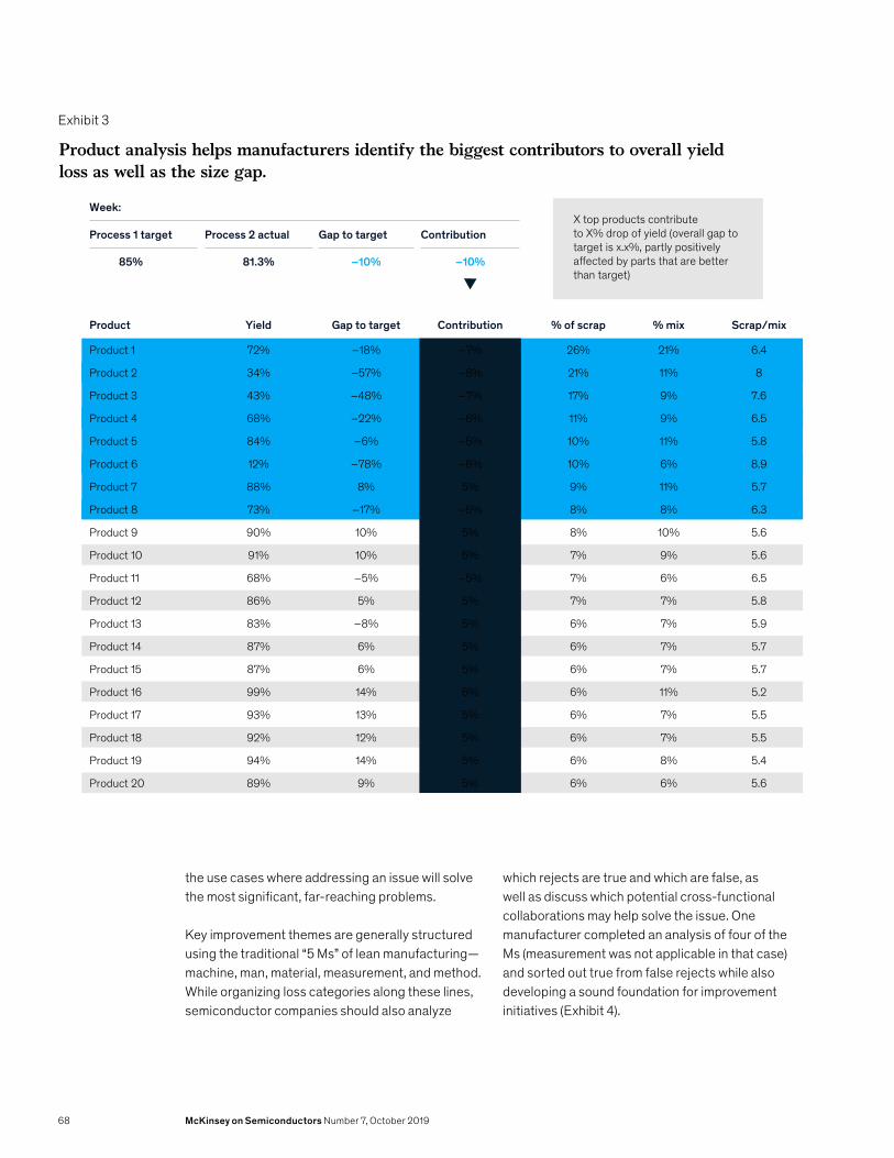
McKinsey Semiconductors 2019Taking the next leapExhibit 3 of 5
Product analysis helps manufacturers identify the biggest contributors to overall yield loss as well as the size gap.
X top products contribute to X% drop of yield (overall gap to target is x.x%, partly positively a�ected by parts that are better than target)
Scrap/mix% of scrapProduct % mixGap to target Yield Contribution
6.426%Product 1 21%–18%72% –7%
821%Product 2 11%–57%34% –8%
7.617%Product 3 9%–48%43% –7%
6.511%Product 4 9%–22%68% –6%
5.810%Product 5 11%–6%84% –5%
8.910%Product 6 6%–78%12% –6%
5.79%Product 7 11%8%88% 5%
6.38%Product 8 8%–17%73% –5%
5.68%Product 9 10%10%90% 5%
5.67%Product 10 9%10%91% 5%
6.57%Product 11 6%–5%68% –5%
5.87%Product 12 7%5%86% 5%
5.96%Product 13 7%–8%83% 5%
5.76%Product 14 7%6%87% 5%
5.76%Product 15 7%6%87% 5%
5.26%Product 16 11%14%99% 6%
5.56%Product 17 7%13%93% 5%
5.56%Product 18 7%12%92% 5%
5.46%Product 19 8%14%94% 5%
5.66%Product 20 6%9%89% 5%
–10%
Gap to target Process 2 actual
85% 81.3% –10%
Week:
Contribution Process 1 target
the use cases where addressing an issue will solve the most significant, far-reaching problems.
Key improvement themes are generally structured using the traditional “5 Ms” of lean manufacturing—machine, man, material, measurement, and method. While organizing loss categories along these lines, semiconductor companies should also analyze
which rejects are true and which are false, as well as discuss which potential cross-functional collaborations may help solve the issue. One manufacturer completed an analysis of four of the Ms (measurement was not applicable in that case) and sorted out true from false rejects while also developing a sound foundation for improvement initiatives (Exhibit 4).
Exhibit 3
68 McKinsey on Semiconductors Number 7, October 2019
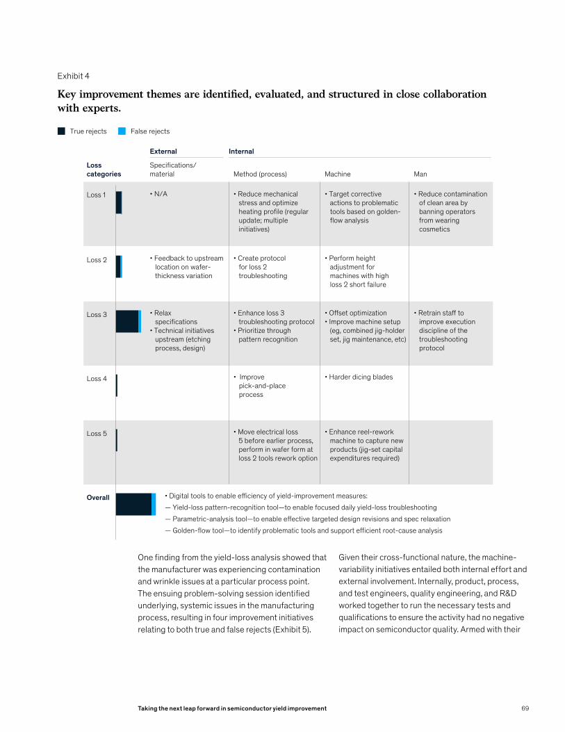
Taking the next leap forward in semiconductor yield improvement
McKinsey Semiconductors 2019Taking the next leapExhibit 4 of 5
Key improvement themes are identi�ed, evaluated, and structured in close collaboration with experts.
Loss categories Machine Method (process) Man
Speci�cations/material
Internal External
False rejects True rejects
• Feedback to upstream location on wafer- thickness variation
• Create protocol for loss 2 troubleshooting
• Perform height adjustment for machines with high loss 2 short failure
Loss 2
• Move electrical loss 5 before earlier process, perform in wafer form at loss 2 tools rework option
• Enhance reel-rework machine to capture new products (jig-set capital expenditures required)
Loss 5
• Relax speci�cations• Technical initiatives upstream (etching process, design)
• Enhance loss 3 troubleshooting protocol • Prioritize through pattern recognition
• O�set optimization• Improve machine setup (eg, combined jig-holder set, jig maintenance, etc)
• Retrain sta� to improve execution discipline of the troubleshooting protocol
Loss 3
• Digital tools to enable e�ciency of yield-improvement measures:— Yield-loss pattern-recognition tool—to enable focused daily yield-loss troubleshooting— Parametric-analysis tool—to enable e�ective targeted design revisions and spec relaxation— Golden-�ow tool—to identify problematic tools and support e�cient root-cause analysis
Overall
• Improve pick-and-place process
• Harder dicing bladesLoss 4
• Reduce mechanical stress and optimize heating pro�le (regular update; multiple initiatives)
• Target corrective actions to problematic tools based on golden- �ow analysis
• Reduce contamination of clean area by banning operators from wearing cosmetics
• N/ALoss 1
One finding from the yield-loss analysis showed that the manufacturer was experiencing contamination and wrinkle issues at a particular process point. The ensuing problem-solving session identified underlying, systemic issues in the manufacturing process, resulting in four improvement initiatives relating to both true and false rejects (Exhibit 5).
Given their cross-functional nature, the machine-variability initiatives entailed both internal effort and external involvement. Internally, product, process, and test engineers, quality engineering, and R&D worked together to run the necessary tests and qualifications to ensure the activity had no negative impact on semiconductor quality. Armed with their
Exhibit 4
69

McKinsey Semiconductors 2019Taking the next leapExhibit 5 of 5
The idea-generation process starts by brainstorming ways to reduce both true and false rejects and focusing on addressable issues.
Developed into initiative
Reject code 2
Reject code 1
Hypothesis tree for process X yield losses
Estimated improvement potential, %
Decrease cost of non-quality at process X
Decrease false rejects
Decrease true rejects
Match internal operational specs at process X to customer specs (no additional further tightening)
Decrease intermachine and interoperator performance variability 16
5
Improve lamination-assembly process (shift from standard to advanced material Y where possible) 9
Adjust tool recipe settings (calibrations) on machines to decrease false rejects 10
Improve baking operational process (root-cause “killer tiles”) in back-end assembly N/A
40
Add incoming mapping of missing dies in front-end manufacturing from upstream site(s) N/A
Improve front-end manufacturing and delivery process from upstream site(s) N/A
Exhibit 5
analysis, engineers could have more meaningful discussions with external vendors about legacy patches to existing equipment and ideas to improve machine performance.
The implementation of these four initiatives reduced contamination rejects for identified products by 90 percent and wrinkle rejects by 40 percent, and in the long term gave valuable insight to engineers on both collaborating with third parties as well as ingraining an ownership mind-set.
Impact on a yield engineer’s typical day, with the holistic view of yield improvementsYield engineering resources are typically spent supporting or leading improvement activities across both product and process engineering. At one manufacturer, yield engineers’ daily activities ranged across three main areas—root-cause problem solving of excursions and other critical identified yield losses, cross-functional yield-improvement activities and collaborations with other
70 McKinsey on Semiconductors Number 7, October 2019
Taking the next leap forward in semiconductor yield improvement
As noted by the CEO of advanced-analytics company Motivo Engineering,
“Each fab has thousands of process steps, which, in turn, have thousands of parameters that can be used in different combinations. With so many factors in play, we see a lot of chip failures or defects.”¹ Given its complexities, traditional quantitative analysis wouldn’t help fabs uncover all improvement opportunities, resulting in a lengthy process of root-issue discovery—and thus massive yield losses.
For that reason, the use of advanced analytics offers a new paradigm for yield improvement in the semiconductor industry. Indeed, the nature of manufacturing complexity means there
is a big difference between insights from traditional quantitative analysis and those from advanced analytics. Furthermore, semiconductor manufacturing is in a unique position compared with other industries to reap the benefits of advanced analytics, given the massive amount of data embedded in fabs’ highly automated and sensor-laden environment. Fabs can benefit from yield analytics through three key levers:
— Early defect detection and root-cause identification. Advanced-analytics tools can help uncover issues much faster and in much greater detail, leading to faster root-
cause identification. This benefit is greater when we try to uncover root causes of low- and medium-frequency errors, which are difficult to detect using traditional analytics.
— Improved value-added time for engineers. At one organization, for example, data pulling and analysis in line-maintenance activities can take up more than triple the time required than if data infrastructure and interface are well designed. This situation represents an opportunity to free up engineers’ time to focus instead on core issues and production design solutions.
teams, and operational tracking and reporting of yield performances across the fab. By applying a holistic approach toward yield improvements based on the steps described above, a typical day in the life of a yield engineer improved in all three realms.
Root-cause problem solving The majority of yield engineering resources used to be spent on yield-loss analyses and low-yield-threshold troubleshooting, for both mature products and new product releases from product development, including buy-off approvals. Due to the yield-loss analysis, the manufacturer’s yield engineers could shift from a reactive “firefighting” stance on tackling ad hoc requests or manufacturing execution system triggers to solving for root causes of major excursions or other weekly yield losses on the line.
Engineers can now identify key losses as per the loss matrix that are unaddressed and start with the
one that will have the biggest forecasted impact to the bottom line. Internal problem solving is further strengthened with the help of big data analytics solutions that proactively highlight commonalities or pattern recognition—for example, a particular tool, process group, or even upstream product or process that contributes significantly to yield losses (see sidebar, “The role of advanced analytics in semiconductor yield improvement: Converting data into actions”). Yield solutions can help push efficiency improvements to the team by providing proactive, low-yield threshold warnings and reporting while also improving turnaround time for lot releases.
Cross-functional yield improvements Previously, resources were spread across multiple projects or initiatives with other engineering teams, with the main task of using analytics to identify the
The role of advanced analytics in semiconductor yield improvement: Converting data into actions
1 For more, see Koen De Backer, Matteo Mancini, and Aditi Sharma, “Optimizing back-end semiconductor manufacturing through Industry 4.0,” February 2017, McKinsey.com.
71

The role of advanced analytics in semiconductor yield improvement: Converting data into actions (continued from page 71)
2 “Yield and yield management,” in Cost Effective IC Manufacturing, Scottsdale, AZ: Integrated Circuit Engineering Corporation,1997.
— Powerful tool for “past learning” and continuous improvement. Machine-learning algorithms, a well-organized data lake, and the appropriate tools allow fabs to accumulate learning from past experiences and enable continuous improvement. Whereas the traditional approach eliminates defects by adjusting multiple parameters, which helps with the current batch, it fails to offer any insight into the root cause of the problem—meaning it is likely to be repeated in future batches.²
Identify core analytics capabilities that can improve yieldSeven core analytics capabilities are important in yield-management solutions: monitoring and reporting, parametric analysis, correlation analysis, golden-flow analysis, equipment optimization, pattern recognition, and event analysis:
— Monitoring and reporting is the most basic among the capabilities—but also one of the most important. This process refers to trend charts, histograms, Pareto analysis, proactive reporting and notification, and enhanced statistical process control, all of which enable enhanced performance
management of the manufacturing process. These tools and processes enable data to be managed and reported by the engineers so it’s most beneficial to their target audience, be they process engineers, managers, or third parties such as customers.
— Parametric analysis refers to testing how product parameters are distributed at performance testing and inspections and comparing these findings to product development’s specification limits. This analysis ultimately aims to enable the optimization of specifications—tight enough to ensure good quality but also reasonable enough to prevent unnecessary over- or under-rejection.
— Correlation analysis finds correlations between test parameters at earlier stages versus final inspections. This assessment aims to maximize final product performance and help manage end-to-end yield by adjusting test parameters depending on how they correlate with testing results, either electrical or visual test parameters.
— Golden-flow analysis is a crucial analytical capability to determine tool commonality and identify which tools are performing at optimal levels—and which are not. These data help with both tool matching and ensuring that production is as high yield and efficient as possible, maximizing throughput and optimizing manufacturing flow (see case study “Golden-flow analysis in action”).
— Equipment optimization as an analytical capability refers to how software can perform predictive analyses to determine potential issues before they occur. This ability is closely linked to predictive maintenance and aims to avoid yield loss by tackling predictable tool variation and necessary parameter tuning.
— Pattern recognition is about looking at the distribution of parameter patterns across wafer maps and connecting the findings to equipment, manufacturing trends, and correlations with process and test parameters. With this capability, live feedback can be given to engineers
72 McKinsey on Semiconductors Number 7, October 2019

Taking the next leap forward in semiconductor yield improvement
McKinsey Semiconductors 2019Taking the next leapExhibit
Commonality analysis helps to identify low-performing and golden tools in situations where trends are unclear.
XYZ-1
Normalized litho-defect density at Tool 1–Tool 2 by lithography tool, number per cm²
Days of week, #
2 1
0.1
7 0
6 5 4 3
0.4
0.2
1.1
0.6
0.3
0.7
0.8
0.9
0.5
1.0
Upper control limit
XYZ-2 XYZ-3
Golden-flow analysis helps identify bad actors and golden tools in situations where trends are unclear. At one manufacturer, the analysis detected that a specific tool (XYZ-1), which was one of three tools in the same class
and configuration, was experiencing an uptick in normalized defect density across different layers over a seven-day period (exhibit). The uptick had not surpassed the upper control limit (UCL), so without the analysis there would have been no
Case study
indicatication of a problem until after it got worse. The advanced warning of increased defect density allowed the manufacturer to take down the tool for investigation, repairs, or calibration interventions.
Golden-flow analysis in action
Exhibit
73

so tools and process parameters can be adjusted to reduce yield loss (see case study “Using analytics to reduce losses”).
— Event analysis entails studying production events, such as maintenance and supply changes, to discover their effect on yield. Identifying root causes for quality shifts or parametric surges can be done by tying them to the occurrence of various events on the manufacturing floor.
Undertake key enablers to overcome typical challenges in implementing yield analyticsWell-organized data integration and interface. Data pull and cleaning (that is, the creation of a data lake) are important steps in deploying analytics. Despite the richness of data gathered through
highly automated and sensor-laden systems in fabs, data quality is usually a challenge in implementing analytics software or using data for analysis; for example, different product families have different data formats and complex production processes. The important step is to get individuals with a strong technical knowledge of data and database optimization to create the right data infrastructure to enable scale-up of analytics solutions.
Right organization setup to take data insights to fast action and feedback loop. Converting data and insights into actions is among the most critical steps—and challenges—to capture benefits from analytics. In particular to yield, issues always cross sites and require end-to-end collaboration to get breakthrough results. The key to success is to have effective yield tracking and a platform to enable
collaboration and action ( see case study “Feedback loop finds costs savings”).
Partnerships with technology and analytics vendors. As our colleagues have noted, many analytics and machine-learning vendors believe that semiconductor companies prefer to develop solutions in-house,³ which discourages them from building strong relationships with other semiconductor companies. In reality, active partnerships with analytics vendors will help increase the speed of building analytics capabilities for fabs. Given the fast-changing environment and highly specialized capability in analytics, ongoing collaboration and partnership will help semiconductor companies stay on the cutting edge and employ solutions that enhance in-house capability.
The role of advanced analytics in semiconductor yield improvement: Converting data into actions (continued from page 72)
3 Ondrej Burkacky, Mark Patel, Nicholas Sergeant, and Christopher Thomas, “Reimagining fabs: Advanced analytics in semiconductor manufacturing,” March 2017, McKinsey.com.
impact of recommended improvements. Armed with end-to-end traceability of yield losses from front end to back end, yield teams benefit from a more granular view of bottom-line impact, reducing the analytical resources needed and allowing for more insights to be shared with the cross-functional team, including R&D, business-unit sales and marketing teams, and front- and back-end managers.
Teams can effectively link decisions from customer requirements (either by R&D or business units), down to bottom-line impact on front-end and back-end expected yield losses, to identify systemic root causes cutting across processes, reject categories, or products. This capability helps yield engineers be more precise in identifying which teams (product or process engineers) are needed and helps to prioritize the initiatives in which they
74 McKinsey on Semiconductors Number 7, October 2019

Taking the next leap forward in semiconductor yield improvement
Feedback loop finds cost savings
One semiconductor player operating across regions in Asia and America set up a cross-site yield project-management office (PMO) to facilitate
end-to-end yield monitoring and speed up the feedback loop. Along with the development of four analytical tools and a performance-management dashboard,
Case study
this yield PMO has delivered 10 percent yield improvement and identified and implemented a $12 million cost-savings opportunity within six months.
One manufacturer developed a false-reject estimator analytics tool for final inspection equipment to help the fab detect and estimate sizes of false rejects based on a pattern-recognition algorithm.
The algorithm provides a daily automated report of false rejects at tool and part number (product) levels, enabling a focused effort to tackle problems in a timely manner by comparing with manual
estimation and monitoring on a monthly basis. This approach reduced losses from material wastes and customer quality issues while enhancing overall capacity (for example, dice output per day).
Case study
Using analytics to reduce losses
ought to invest most of their time. From an efficiency improvement and workload-reduction perspective, teams can better rationalize meeting participation.
Yield engineers are further empowered with data to highlight potential opportunities to implement more yield gains by aligning or relaxing internal specifications, without affecting customer demand or satisfaction. Transparency enables teams across
the value chain to collaborate on more data and to push initiatives to be more fact based and prioritize resources to maximize profitability.
Yield-performance tracking and reporting For both mature and new unreleased products, yield engineers have shifted from daily or weekly yield-percentage monitoring to more continuous monitoring thanks to the capabilities of the loss
75

Copyright © 2019 McKinsey & Company. All rights reserved.
Koen De Backer is an alumnus of McKinsey’s Singapore office, where Matteo Mancini is a partner. RJ Huang is a consultant in the Manila office, Mantana Lertchaitawee is a consultant in the Bangkok office, and Choon Liang Tan is an alumnus of the Kuala Lumpur office.
matrix. Performance baselines and improvements can be tracked and reported either in the form of the loss matrix or with the help of analytical yield solutions. Teams can now visualize the distribution of key forecasted shifts in yield losses as measured by monetary impact, which helps prioritize the next wave of improvement initiatives. Reporting is more mutually exclusive and collectively exhaustive than previously limited reporting by process and integral yield percentages.
For semiconductor companies, the successes of effective yield improvement lead not only to increased profitability but also to better organizational health as a whole. Our experience points to three central key pillars that make yield transformations successful:
— Align the language and data of engineering and finance. Looking at yield percentages only provides one view of the situation; engineering and finance alike must align on using the cost of poor quality as the method for understanding and guiding the direction of the company’s yield improvement efforts. Collaboration on the creation of a CONQ calculation can ensure that improvement initiatives are based on a viable foundation of data and collaboration.
— Develop a holistic, data-driven view of what needs to improve and where. Work on yield can often be siloed due to how manufacturing organizations are structured. Using the loss matrix and analytical solutions—where costs can be easily viewed by processes, reject codes, or products—allows engineers and managers to gain a better view of the health of the entire manufacturing process, from R&D through wafer fabrication and die packaging, to push improvement efforts to the right areas. This view also gives engineers and managers a chance to track what areas they are already tackling, as well as what areas have yet to be explored.
— Implement systemic improvements. Yield improvements should address excursion cases—but more important, they should also tackle the baseline yield. By setting up discussions where engineers can explore historic causes of yield loss, new levers can be discovered that will increase overall yield performance for a certain product or process. There can also be situations where certain losses are tolerated simply because they have historically been seen as acceptable. Focusing on standout issues of yield loss, as well as working to continuously improve the baseline yield percentage as a whole, leads to more sustainable yield improvement.
76 McKinsey on Semiconductors Number 7, October 2019


This McKinsey Practice Publication meets the Forest Stewardship Council® (FSC®) chain-of-custody standards. The paper used in this publication is certified as being produced in an environmentally responsible, socially beneficial, and economically viable way.
Printed in the United States of America
November 2019Designed by Global Editorial ServicesCopyright © McKinsey & CompanyMcKinsey.com