master thesis design and analysis of 60 kw dc-dc...
TRANSCRIPT
Master Thesis
Design and Analysis of 60 kW DC-DC Converter for Hybrid Electric Vehicle
Applications.
Students : Muhammad Rafiq
Mohammed Fareed Ul Hasan
Supervisor
& examiner : Prof. Torbjörn Thiringer
Electric Power Engineering
Chalmers University of Technology, Göteborg
Abstract
i
ABSTRACT
This thesis deals with the design and analysis of dc-dc converter with different core materials,
core shapes, voltage levels and frequencies. The losses and efficiency of the converter is
investigated. Furthermore the weight and losses of the converter are studied at different
frequencies.
Analytical results shows that losses are higher in the 900 V system as compared to the 450V
system.The analysis also shows that by increasing the operating frequency, the losses increases
but the weight of the converter is reduced. A comparison of the two voltage level systems as
proposed in the report shows that the two voltage systems behaves differently at different power
losses but it is noted that the low voltage system is more energy efficient. The result suggests that
the use of iron powder as core material reduces the weight of the converter. The result also
shows that the core shape ETD-59 has smaller core losses as compared with the EC-70 core
shape.

Acknoledgment
ii
ACKNOWLEDGMENT
First, we would like to thank our examiner Professor Torbjörn Thiringer for his great help and
support throughout our thesis work. We would like to thanks all the people in the department
especially who helped us, Sonja Lundmark, Oskar Josefsson, Andreas Karvonen and Saeid
Haghbin. At last but not the least, we would wish to thank the Jan-Olov Lantto which helped us a
lot with our work station problems.
Contents
iii
CONTENTS
ABSTRACT ..................................................................................................................................... i
ACKNOWLEDGMENT................................................................................................................. ii
LIST OF SYMBOLS ...................................................................................................................... v
1 INTRODUCTION ....................................................................................................................... 1
1.1 Background ...................................................................................................................... 1
1.2 Purpose of work ............................................................................................................... 1
2 SYSTEM OVERVIEW ............................................................................................................... 3
2.1 The Hybrid Electrical Vehicle ............................................................................................ 3
2.2 Bidirectional boost converter .............................................................................................. 4
2.2.1 Generating mode ............................................................................................................. 5
2.2.2 Motoring mode................................................................................................................ 7
3 SEMICONDUCTOR LOSS CALCULATION OF THE CONVERTER ................................. 11
3.1 IGBT and Diode Losses .................................................................................................. 11
3.1.1 Conduction Losses .................................................................................................... 11
3.1.2 Switching losses ....................................................................................................... 13
4 BATTERY ................................................................................................................................. 15
4.1 The hybrid vehicle battery .................................................................................................. 15
4.2 Battery technology .............................................................................................................. 15
4.3 Characteristics of Li-ion batteries ....................................................................................... 15
4.4 Charge ................................................................................................................................. 16
4.5 HEV Batteries ..................................................................................................................... 16
5 DESIGN ..................................................................................................................................... 17
5.1 Design of the inductor ......................................................................................................... 17
Parameters: ............................................................................................................................ 17
Core material, shape and size ................................................................................................ 17
5.2 Design of Capacitors ........................................................................................................... 19
6 CASE SET UP ........................................................................................................................... 21
6.1 Base design ......................................................................................................................... 21
Converter parameters ............................................................................................................ 21
6.1.1 Boost/Motoring mode .................................................................................................. 21
6.1.2 Buck/Generating mode ................................................................................................ 28
Contents
iv
7 ANALYSIS ................................................................................................................................ 35
7.1 Mode of Operation .............................................................................................................. 35
7.2 Core material ....................................................................................................................... 35
7.3 Core shape ........................................................................................................................... 35
7.4Voltage level ........................................................................................................................ 35
7.5 Switching frequency ........................................................................................................... 35
Case 1.1: Ferrite material, (EC-70) for (450V System) ........................................................ 36
Case 1.2: Ferrite material, (ETD-59) for (450V System) ..................................................... 40
Case 1.3: Ferrite material, (EC-70) for (900V System) ........................................................ 42
Case 1.4: Ferrite material, (ETD-59) for (900V System) ..................................................... 44
Case 2.1: Iron powder material, (EC-70) for (450V System) .............................................. 46
Case 2.2: Iron powder material, (ETD-59) for (450V System) ............................................ 48
Case 2.3: Iron powder material, (EC-70) for (900V System) ............................................... 50
Case 2.4: Iron powder material, (ETD-59) for (900V System) ............................................ 52
8 CONCLUSION .......................................................................................................................... 57
REFERENCES ............................................................................................................................. 59
List of symbols
v
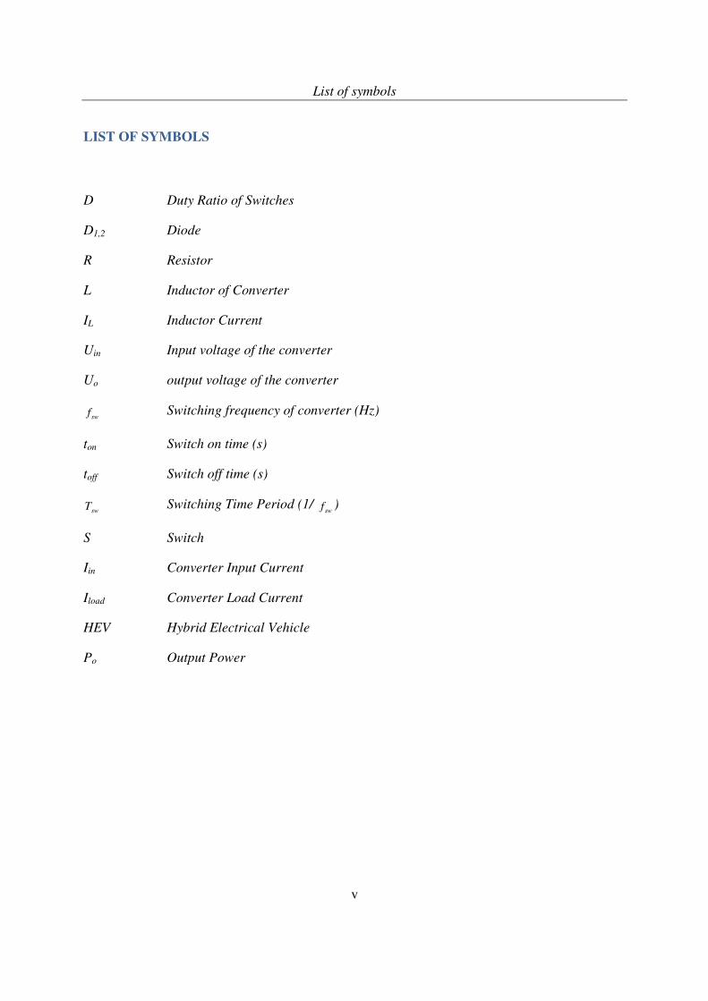
LIST OF SYMBOLS
D Duty Ratio of Switches
D1,2 Diode
R Resistor
L Inductor of Converter
IL Inductor Current
Uin Input voltage of the converter
Uo output voltage of the converter
swf Switching frequency of converter (Hz)
ton Switch on time (s)
toff Switch off time (s)
swT Switching Time Period (1/ swf )
S Switch
Iin Converter Input Current
Iload Converter Load Current
HEV Hybrid Electrical Vehicle
Po Output Power

List of symbols
vi
Introduction
1
1 INTRODUCTION
1.1 Background
A critical factor propelling the shift from conventional gasoline/diesel engine vehicles to electric
hybrid and fuel cell vehicles is the improvement in performance, size and cost of power
electronics circuits over the past decade, with parallel improvements in sensors and
microprocessors.
Typical power electronic circuits used in hybrid electric vehicles (HEV) include inverters and
DC-DC converters. In some electrical vehicles the high voltage battery is connected directly to
the inverters, however an alternate is to have a dc/dc converter in between to maintain a fixed dc
voltage for the inverter. In this project we provide topology, design and analysis of this DC-DC
converter for hybrid electrical vehicle applications (HEV).
1.2 Purpose of work
The purpose of this project is to design and analysis of a 60KW DC-DC converter for hybrid
electric vehicle applications. This converter is able to maintain a constant DC link voltage when
it is in motoring (or Up) mode of operation and energy flows from the DC voltage link bus to the
battery when it works in generating (Down) mode of operation. The aim is to study the operation
of the DC-DC converter at different switching frequencies respectively 10 and 20 kHz and
different core materials with two different shapes for the inductor. The objective is to analyze
losses and weight at different frequencies as well as analyze the efficiency at different power
levels.

Introduction
2
System overview
3
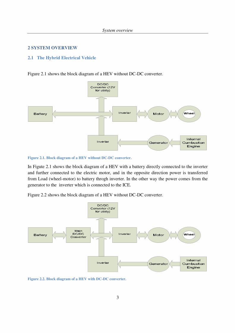
2 SYSTEM OVERVIEW
2.1 The Hybrid Electrical Vehicle
Figure 2.1 shows the block diagram of a HEV without DC-DC converter.
Figure 2.1. Block diagram of a HEV without DC-DC converter.
In Figute 2.1 shows the block diagram of a HEV with a battery directly connected to the inverter
and further connected to the electric motor, and in the opposite direction power is transferred
from Load (wheel-motor) to battery throgh inverter. In the other way the power comes from the
generator to the inverter which is connected to the ICE.
Figure 2.2 shows the block diagram of a HEV without DC-DC converter.
Figure 2.2. Block diagram of a HEV with DC-DC converter.
System overview
4
The DC-DC converter in a HEV is used to maintain a constant dc link voltage and to step up and
step down the voltage as shown in Figure 2.2.
There are many different potential HEV configurations, but in general a HEV has an electric
drive train like an EV, plus an internal combustion engine (ICE) that can charge the batteries
periodically as is shown in Figure 2.2. The internal combustion engine is most efficient for a
small range of operating conditions. This is utilized in HEV where the internal combustion
engine can be made to operate at this efficient operating point. The HEV can operate the internal
combustion engine (ICE) at its most efficient point for charging of the battery and can use the
drive train to take up all the slack under other conditions. The emissions are lower than the
combustion engine driving the car by itself and fuel economy can be significantly improved. The
usable range of Electrical vehicles can be extended by hybrid technologies. A hybrid would
allow the vehicle to operate in an urban/polluted area with only batteries and then switch to the
engine outside the urban area.
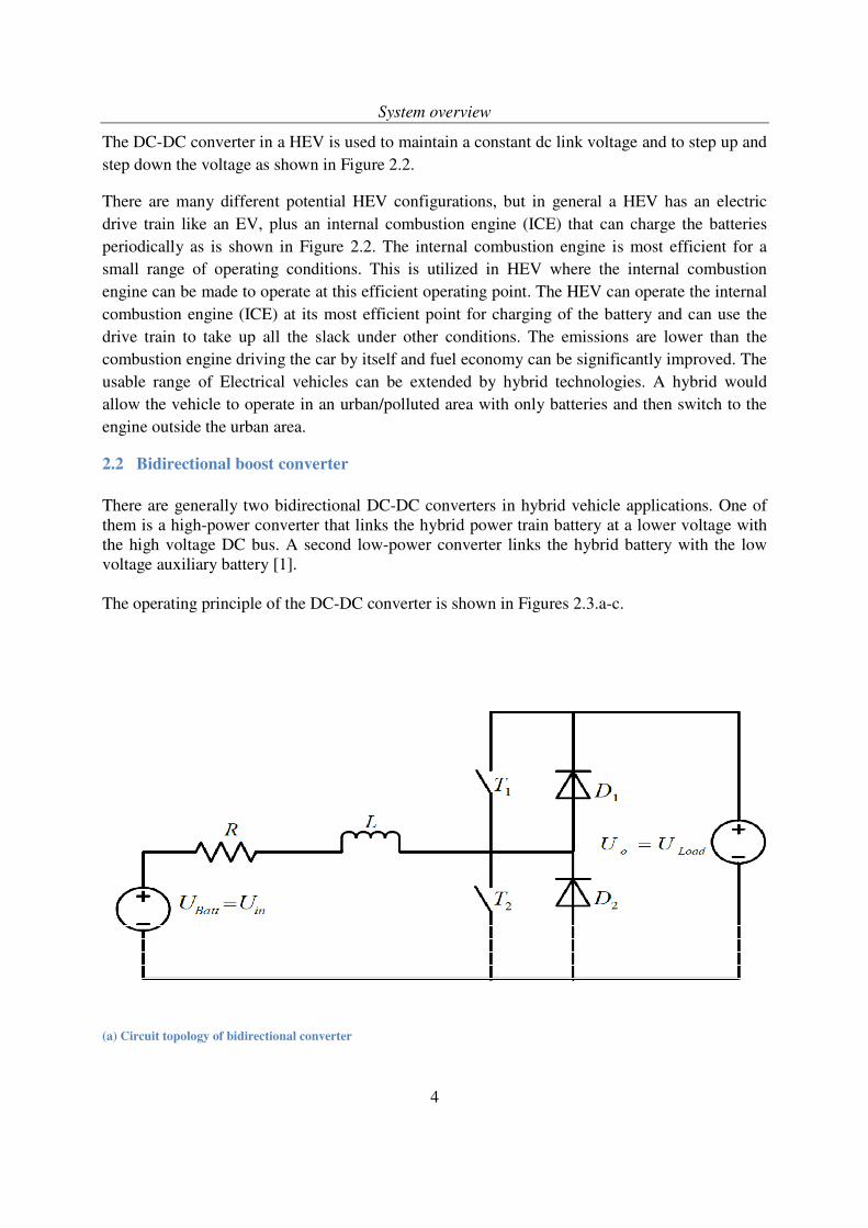
2.2 Bidirectional boost converter
There are generally two bidirectional DC-DC converters in hybrid vehicle applications. One of
them is a high-power converter that links the hybrid power train battery at a lower voltage with
the high voltage DC bus. A second low-power converter links the hybrid battery with the low
voltage auxiliary battery [1].
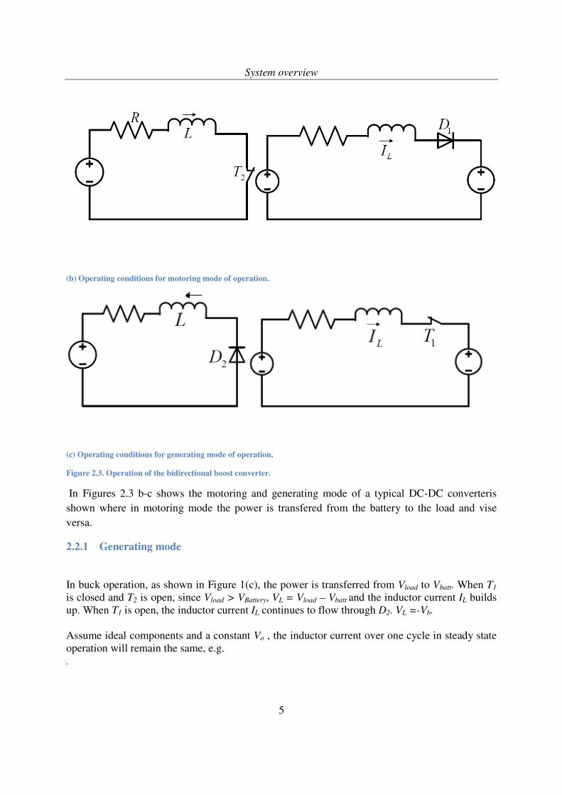
The operating principle of the DC-DC converter is shown in Figures 2.3.a-c.
(a) Circuit topology of bidirectional converter
System overview
5
(b) Operating conditions for motoring mode of operation.
(c) Operating conditions for generating mode of operation.
Figure 2.3. Operation of the bidirectional boost converter.
In Figures 2.3 b-c shows the motoring and generating mode of a typical DC-DC converteris
shown where in motoring mode the power is transfered from the battery to the load and vise
versa.
2.2.1 Generating mode
In buck operation, as shown in Figure 1(c), the power is transferred from Vload to Vbatt. When T1
is closed and T2 is open, since Vload > VBattery, VL = Vload – Vbatt and the inductor current IL builds
up. When T1 is open, the inductor current IL continues to flow through D2. VL =-Vb.
Assume ideal components and a constant Vo , the inductor current over one cycle in steady state
operation will remain the same, e.g.
.
System overview
6
)()(
11
1
1
0
∫∫+
−=−
offtont
ont
LinkDCDCLinkBattery
ont
VdtVV (2.1)
BatteryBatteryo VDVT
ontV 1
1== (2.2)
where D1 is the duty ratio defined as the percentage of on-time of switch T1
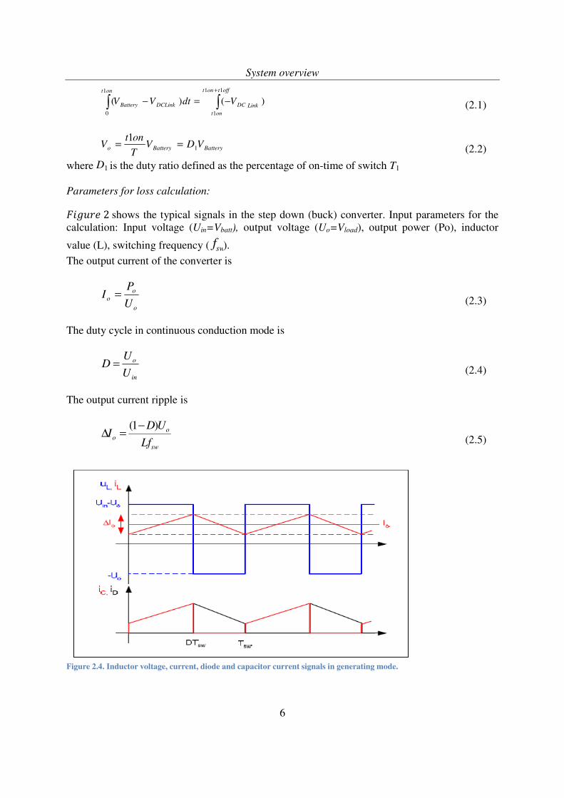
Parameters for loss calculation:
2 shows the typical signals in the step down (buck) converter. Input parameters for the
calculation: Input voltage (Uin=Vbatt), output voltage (Uo=Vload), output power (Po), inductor
value (L), switching frequency ( swf ).
The output current of the converter is
o
o
oU
PI =
(2.3)
The duty cycle in continuous conduction mode is
in
o
U
UD =
(2.4)
The output current ripple is
sw
o
oLf
UDI
)1( −=∆
(2.5)
Figure 2.4. Inductor voltage, current, diode and capacitor current signals in generating mode.
System overview
7
In Figure 2.4 shows the typical signals of inductor voltage, inductor current, capacitor current,
diode current input and output voltages.
The parameters needed for the loss calculation can be determined as
2
o
ocon
III
∆−=
(2.6)
2
o
ocoff
III
∆+=
(2.7)
ocav DII =
(2.8)
ocrms DII 22 = (2.9)
oDav IDI )1( −=
(2.10)
oDrms IDI 22 )1( −=
(2.11)
2.2.2 Motoring mode
In this operation, the power is transferred from VBattery to VDC Link. When T2 is closed and T1 is
open, the output voltage capacitor and inductor form a direct path through switch T2 as shown in
Figure 1 (a &d). Therefore VL =-VBattery and the inductor current IL builds up. When T1 is open,
the inductor current continues to flow through D1 to Vd, therefore VL = VDC Link –VBattery.
Assume ideal components and a constant Vd, the inductor current over one cycle in steady state
will remain the same, e.g.
∫∫+
−=
offtont
ont
DCLinkBattery
ont
DCLink dtVVdtV
22
2
2
0
)()(
(2.12)
BatteryDCLink VD
V−
=1
1
(2.13)
where D is the duty ratio defend as the percentage of the on-time of switch T2
System overview
8
T
tD on2=
(2.14)
Parameters for loss calculation:
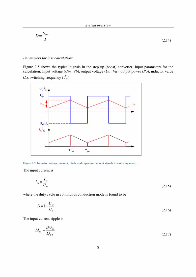
Figure 2.5 shows the typical signals in the step up (boost) converter. Input parameters for the
calculation: Input voltage (Uin=Vb), output voltage (Uo=Vd), output power (Po), inductor value
(L), switching frequency ( swf ).
Figure 2.5. Inductor voltage, current, diode and capacitor current signals in motoring mode.
The input current is
in
in
inU
PI =
(2.15)
where the duty cycle in continuous conduction mode is found to be
o
in
U
UD −=1
(2.16)
The input current ripple is
SW
in
inLf
DUI =∆
(2.17)
System overview
9
The parameters needed for the loss calculation can be determined as
2
in
incon
III
∆−=
(2.18)
2
in
incoff
III
∆+=
(2.19)
incav DII =
(2.20)
incrms IDI )1(2 −=
(2.21)
inDav IDI )1( −=
(2.22)
inDrms IDI 22 )1( −=
(2.23)

System overview
10
Semiconddutor loss calculation of the converter
11
3 SEMICONDUCTOR LOSS CALCULATION OF THE CONVERTER
3.1 IGBT and Diode Losses
The IGBT and diode power losses as well as the power losses in any semiconductor component
can be divided in three groups:
a) Conduction losses ( conductionP )
b) Switching losses (swP )
c) Blocking leakage losses usually neglected
Therefore orsemicondutP = conductionP + swP
3.1.1 Conduction Losses
3.1.1 (a) IGBT conduction losses
The IGBT conduction losses can be calculated using an IGBT voltage drop behavior
approximation with a series connection of a DC voltage source representing the IGBT on state
zero current collector emitter voltage and collector on state resistance (.Cr ) [2] as
CCCECCE iruiu += 0)( (3.1)
The important parameters can be read directly from the IGBT datasheet. The 0CE
u and values
can be read from the diagram. The instantaneous value of the IGBT conduction losses are
)()()()()( 2
0 tirtiutitutP CCCCECCECT +== (3.2)
The average IGBT current value is cavI and value of IGBT current is
crmsI . Then the average
power losses can then be expressed as
2
0
2
0
0
0
)()((1
)(1
)( crmsCcavCECCC
T
CE
T
SWSW
CT IrIudttirtiuT
dttpT
tPSWSW
+=+== ∫∫
(3.3)
Semiconddutor loss calculation of the converter
12
3.1.1 (b) Diode conduction losses
The same approximation can be used for the anti-parallel diode as is used for IGBT, giving
DDDDD iruiu += 0)( (3.4)
The instantaneous value of the diode conduction losses is
)()(.)()()( 2
0 tirtiutitutP DDFDDDCD +== (3.5)
If the average diode current is DavI and the rms diode current is
DrmsI , the average diode
conduction losses across the switching period(SWT =1/ swf ) are
DrmsDDavDDDD
T
D
T
SWSW
CD IrIudttirtiuT
dttpT
tPSWSW
2
0
2
0
0
0
)()((1
)(1
)( +=+== ∫∫
(3.6)
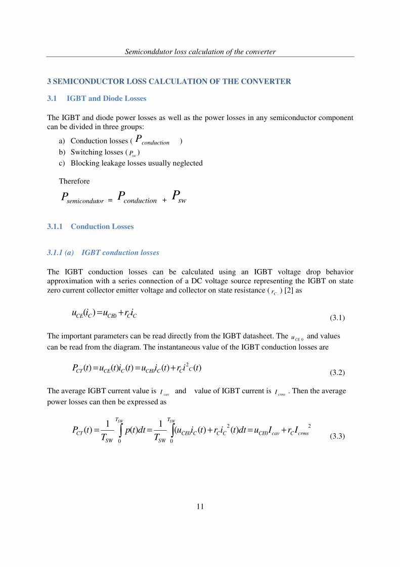
The value of 0CEu and
0Du can be read from the datasheet as following. The Cr and
Dr values
can also be calculated from the datasheet by taking the slope of the desired line of characteristics
as shown in Figure 3.1.
Figure 3.1. Shows how to read the initial voltage and resistance values from the graph of a transistor.
From Figure 3.1 can be seen that how to read the values of 0CEu and
Cr .
Semiconddutor loss calculation of the converter
13
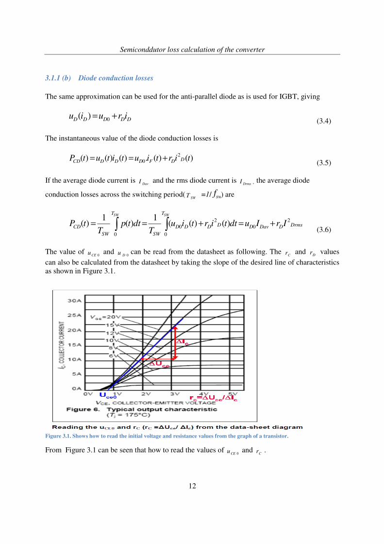
Figure 3.2 Shows how to read the initial voltage and resistance values from the graph of a diode.
From Figure 3.2 seen that how to read the values of 0Du and
Dr .
3.1.2 Switching losses
The switching losses in the IGBT and the diode are the product of the switching energies and the
switching frequency swf
swoffMonMswM fEEP )( += (3.7)
swoffDonDswD fEEP )( += (3.8)
where the energy during on and off period can be written as
refref
ininrefononM
IV
IVEE
∆=
(3.9)
refref
ininrefoffoffM
IV
IVEE
∆=
(3.10)
where refV and refI are taken from datasheet of IGBT and inV∆ and
inI are the output voltage and
current respectively.
refonE and refoffE can be calculated from the following typical switching losses of the
IGBTaccording to Figure 3.3.
Semiconddutor loss calculation of the converter
14
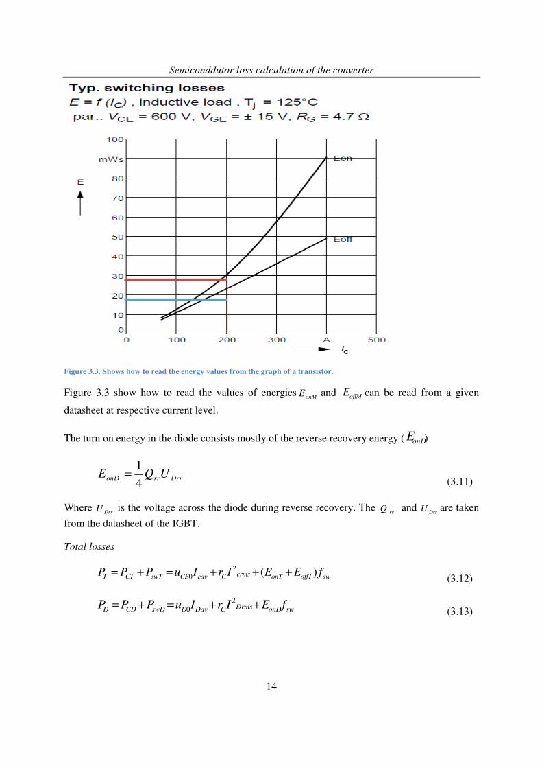
Figure 3.3. Shows how to read the energy values from the graph of a transistor.
Figure 3.3 show how to read the values of energiesonME and offME can be read from a given
datasheet at respective current level.
The turn on energy in the diode consists mostly of the reverse recovery energy ( onDE )
DrrrronD UQE4
1=
(3.11)
Where DrrU is the voltage across the diode during reverse recovery. The
rrQ and DrrU are taken
from the datasheet of the IGBT.
Total losses
swoffTonTcrmsCcavCEswTCTT fEEIrIuPPP )(2
0 +++=+= (3.12)
swonDDrmsCDavDswDCDD fEIrIuPPP ++=+= 2
0 (3.13)
Battery
15
4 BATTERY
4.1 The hybrid vehicle battery
A hybrid vehicle battery is like any other battery except that it is always rechargeable and have
power to propel a large heavy vehicle.
Hybrid vehicle batteries have two electrodes like other batteries (which collect or emit electric
charge) which are lying in a ion rich solution called the electrolyte. The electrodes are separated
from a thin polymer film called a separator which prevents them from touching [3].
A battery is actually a battery pack consisting of many individuals cells. A mobile phone battery
is a single cell and a laptop battery consists of multiple cells working together.
4.2 Battery technology
The battery technology which is becoming most popular in hybrid electrical vehicles is the Li-
ion (lithium-ion battery) technology.
4.3 Characteristics of Li-ion batteries
The battery voltage varies according to the kind of battery selected. For the DC/DC converter,
the voltages used are between 300V and 400V. The peak power is selected to 60kW.
Small lithium ion batteries are widely used in notebook computers, mobile phones, cameras and
other electronic equipment owing to their high energy density. Lithium cobalt oxide is used for
anode in these small batteries but it is not used due to the high price of cobalt in large batteries
used in vehicles. Lithium manganese oxide is used instead which is much cheaper. Manganese-
based Li-ion batteries also have the following important characteristics for application to
vehicles.
• Their charging/discharging efficiency and energy efficiency is high.
• A high single-cell voltage (three times that of Ni-MH batteries and twice that of lead-cid
Batteries) which means less number of cells in the battery.
• The state of charge (SOC) can be sensed easily, so charging durations can be managed
and driving ranges can be accurately predicted.
Battery
16
4.4 Charge
During discharging, lithium ions Li+ carry the current from the negative to the positive electrode,
through the non aqueous electrolyte and separator diaphragm [4].
During charging, an external electrical power source (the charging circuit) applies a higher
voltage (but of the same polarity) than that produced by the battery, forcing the electrical current
to pass in the reverse direction. The lithium ions then migrate from the positive to the negative
electrode, where they become embedded in the porous electrode material in a process known as
intercalation.
4.5 HEV Batteries
High output performance is a key component for HEV batteries. Large amount of regenerative
breaking power make input (charging) performance equally important for truck, buses or other
heavy duty HEVs. The specific energy, specific power, specific recharge power and battery
capacity must be carefully established to match the output required by the motor, the
regenerative breaking performance and hybrid system configuration (series or parallel) [5].
Design
17
5 DESIGN
Inductors are not commercially available readymade for these power levels and it has to be
designed for this particular application. In, this chapter, an inductor is designed [6].
5.1 Design of the inductor
Parameters:
The average current of the Inductor
in
AVGV
PI
∆=
(5.1)
The ripple current can be calculated as
2
minmax III
−=∆
(5.2)
where maximum and minimum currents can be calculated as
2
2.0max
III += and 2
2.0min
III −=
where switching frequency = f (Hz)
Inductance of the indutor = L (µH)
fLZinductor Π= 2 (5.3)
RN
RNIΨ
=Φ=
(5.4)
R
N
INI
2
=Ψ
=
(5.5)
Core material, shape and size
Effective area in square meters is = eA
Effective length in meters is = el
Mass in grams = m
Design
18
Volume in cubic meters = eV
Relative permeability of the material = rµ
Scaling factor = fS
Permeability constant = oµ
Current density = J (A/mm2)
Reluctance for the iron part
ero
e
feA
lR
µµ=
(5.6)
where air gap for coil = airl
Reluctance for the air gap
ero
air
airA
lR
µµ=
(5.7)
The required number of turns
LRN = (5.8)
Total reluctance must be
airfe RRR += (5.9)
The total flux in the core can be calculated as
R
NI=Φ (5.10)
The total flux density in the core can be calculated as
AB
Φ=
(5.11)
Conductor size can be calculated as
Design
19
J
IA in
c = (5.12)
Change in flux density
eRA
INB
∆=∆
(5.13)
The iron losses
efactorfe VlP = (5.14)
where peakB and loss factor is obtained from datasheet.
Copper resistance
c
W
cuA
lR ρ=
(5.15)
Winding length
ww NLl = (5.16)
where turn length can be found from datasheet.
Copper losses
2
incucu IRP = (5.17)
Total inductor losses
cufetotal PPP += (5.18)
5.2 Design of Capacitors
Input capacitor ( InputC ):
The InputC can be calculated by the following formula
Design
20
o
swL
InputV
TIC
∆
∆=
8 (5.19)
where ∆Vois peak-to-peak voltage ripple of the buck converter output (1 to 2 % of the output
voltage).
Output capacitor ( OutputC ):
The OutputC can be calculated by the following formula
o
swoOutput
V
DTIC
∆=
(5.20)
where ∆Vo is peak-to-peak voltage ripple of the boost converter output (1 to 2 % of the output
voltage).
Case set up
21
6 CASE SET UP
6.1 Base design
Converter parameters
P=60 kW
Vinput=300-400 V
Voutput=450 V
f =20 kHz
6.1.1 Boost/Motoring mode
The duty cycle is found as follows
1 inV∆
oV 0.333
(6.1)
The input current of the converter is
inI
inV∆ 200
(6.2)
and the maximum and minimum current can be calculated as follows
maxI inI inI∆
220
(6.3)
minI inI inI∆
180
(6.4)
and the ripple current can be found as
AII
I 202
minmax =−
=∆
The average and rms currents of the IGBT and diode can be calculated as
The average current for IGBT is
Case set up
22
cavI inDI 67
(6.5)
and the rms current is
crmsI inID 116 (6.6)
The average current for diode is
DavI inID)1( − 134
(6.7)
and rms current is
DrmsI inID)1( − 164 (6.8)
Conduction losses
If the average IGBT current value is cavI and the rms value of IGBT current is crmsI as
calculated above, then the average losses can be expressed as
2
0)( crmsCcavCECT IrIutP += 120
(6.9)
The values of 0CEu and Cr (C
CE
CI
Ur
∆
∆= ) from the typical output characteristics
)( CEC UfI = taken from the IGBT data sheet. [7]
the conduction losses of a diode can be calculated as
DrmsDDavDCD IrIutP2
0)( += 145 (6.10)
The value of 0Du can be read from the datasheet and Dr values can also be calculated from the
datasheet by taking the slope of the desired line of characteristics.
Switching losses
The switching losses of the IGBT can be calculated using the onTE and offTE as
Case set up
23
JIV
IVEE
refref
inin
refononT 0043.0=∆
=
(6.11)
JIV
IVEE
refref
inin
refoffoffT 0073.0=∆
=
(6.12)
where refV and refI are taken from datasheet of IGBT and V and Iare the output voltage and
current respectively.
swoffTonTswT fEEP )( += 234
(6.13)
when the switching frequency at 20 kHz.
So the total IGBT losses are
SWConductionT PPP += 354
(6.14)
The diode switching losses are
swoffDonDswD fEEP )( += 93
(6.15)
where onDE can be calculated as
JIV
IVEE
refref
inin
ErrrefonD 0047.0=∆
=
(6.16)
and the switch off losses in the diode are usually )0( ≈offDE neglected, then the total diode losses
are
SWConductionD PPP += 238
(6.17)
So the total semiconductor losses are
DTtorSemiconduc PPP += 59
(6.18)
Case set up
24
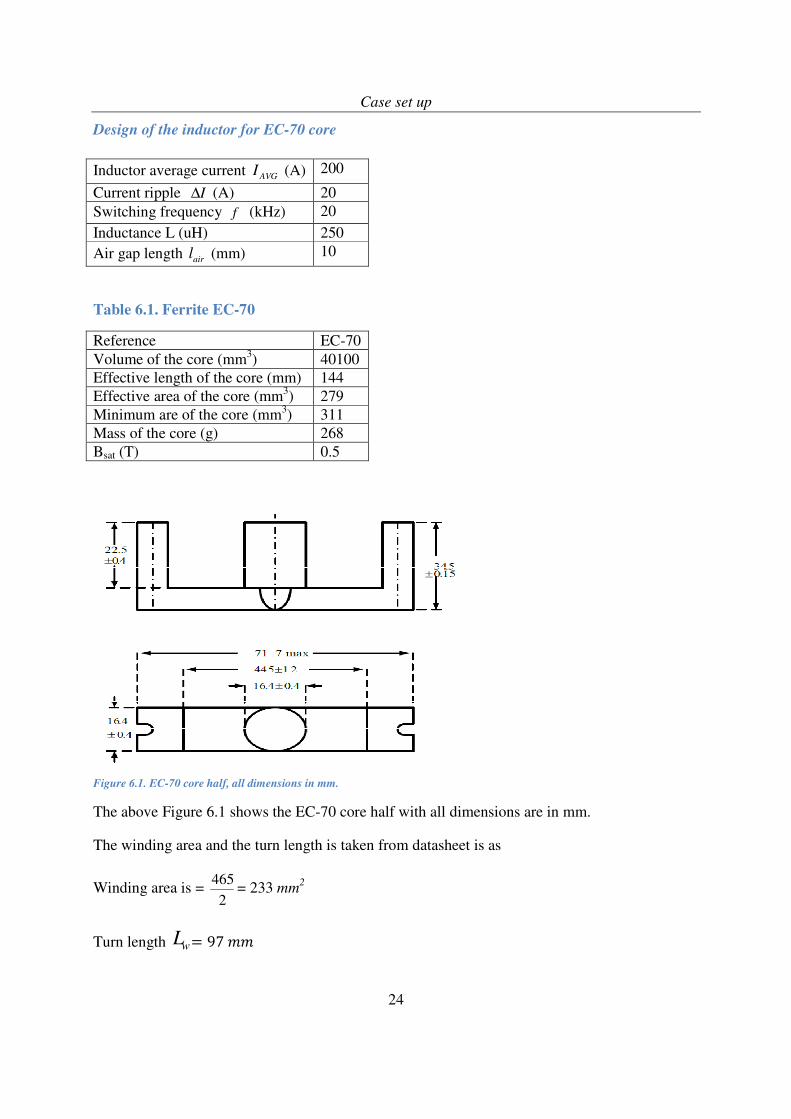
Design of the inductor for EC-70 core
Inductor average current AVGI (A) 200
Current ripple I∆ (A) 20
Switching frequency f (kHz) 20
Inductance L (uH) 250
Air gap length airl (mm) 10
Table 6.1. Ferrite EC-70
Reference EC-70
Volume of the core (mm3) 40100
Effective length of the core (mm) 144
Effective area of the core (mm3) 279
Minimum are of the core (mm3) 311
Mass of the core (g) 268
Bsat (T) 0.5
Figure 6.1. EC-70 core half, all dimensions in mm.
The above Figure 6.1 shows the EC-70 core half with all dimensions are in mm.
The winding area and the turn length is taken from datasheet is as
Winding area is = 2
465= 233 mm
2
Turn length wL 97
Case set up
25
We have to scale the core according to our converter requirements so we will use a scale factor
Scaling factor 49.3=fS
So with scaling factor the parameters of the core will be
eA 3398 2
el 5025
11.39
eV 1704592 3
Winding Area WA 2831
2
Turn length wL = mm57.339
61025.1 −×=oµ
Coil for 20A ripple current
Reluctance of iron part
ero
e
feA
l
µµ=ℜ = WbAT /105168.1 6×
(6.19)
Air gap length mmlair 10=
Reluctance of air gap
WbATA
l
ero
air
air /103542.2 6×==ℜµµ
(6.20)
The total reluctance of the core is
WbATairfe /108710.3 6×=ℜ+ℜ=ℜ
(6.21)
Number of turns
turnsLRN 32== (6.22)
Case set up
26
Total flux
Φℜ
inNI 0.0016
(6.23)
Flux density
TA
Be
47.0=Φ
=
(6.24)
Conductor size = 267.66
3mm
I in = (6.25)
The required conductor area22133mmNAA condc ===
(6.26)
Fill factor 73.0==wd
cond
A
A
(6.27)
The flux density ripple can be calculated as
TA
INB
e
04.0=ℜ
∆=∆
(6.28)
Inductor losses
The iron losses are
WVlP efactorfe 120==
(6.29)
where the ‘lossfactor’ lfactor is taken from the iron powder material graph at different
frequencies [8].
Winding length mNLl ww 88.10==
(6.30)
Copper resistance
Case set up
27
Ω== 0028.0c
w
cuA
lR ρ
(6.31)
Copper losses
WRIP cuincu 3772 ==
(6.32)
Total inductor losses
WPPP cufeinductor 496=+=
(6.33)
Filter losses
WRIPFilter 2.32 =∆=
(6.34)
Total converter losses
WPPPP FilterinductororeSmiconductloss 1090=++=
(6.35)
Efficiency of the converter at full load
%18.98=−
=P
PP losesη
(6.36)
Case set up
28
6.1.2 Buck/Generating mode
Converter parameters:
kWP 60=
VV input 450=
VVoutput 300=
fsw =20 kHz
The duty cycle is found as follows
The duty cycle is
666.0=∆
=in
o
V
VD
(6.37)
The output current is
AIo 150=
The ripple current can be found as
AI 15=∆
The value of inductance will be as follows
HfI
VDL o µ340
)1(=
×∆
∆−=
(6.38)
Conduction losses
The average current of IGBT can be found as
ADII ocav 100==
(6.39)
The rms value of current for IGBT is as
AIDI ocrms 122== (6.40)
Case set up
29
The average value of diode can be found as
AIDI oDav 50)1( =−=
(6.41)
The rms value of current for diode can be found as
AIDI oDrms 87)1( =−=
(6.42)
The conduction losses for IGBT are as follows
WIrIutP crmsCcavCECT 162)(2
0 =+=
(6.43)
And conducation losses for diode are
WIrIutP DrmsDDavDCD 52)( 2
0 =+=
(6.44)
The values of 0CE
u and C
r (C
CE
CI
Ur
∆
∆= ) are taken from the typ. output characteristics
)( CEC UfI = of IGBT data sheet [7].
Switching losses
The onTE and offTE can be calculated as follows
JIV
IVEE
refref
inin
refononT 0043.0=∆
=
(6.45)
and
JIV
IVEE
refref
inin
refoffoffT 0073.0=∆
=
(6.46)
where refV and refI are taken from datasheet of IGBT and V and Iare the output voltage and
current respectively. The switching losses can be calculated as follows
Case set up
30
WfEEP swoffTonTswT 34.233)( =+=
(6.47)
The diode switching losses are
WfEEP offDonDswD 94)( =+=
(6.48)
where onD
E can be calculated as
JIV
IVEE
refref
inin
ErrrefonD 0047.0=∆
=
(6.49)
and the switch off losses in the diode are normally )0( ≈offDE when the frequency 20 kHz.
So the total IGBT losses are
WPPP SWConductionT 396=+=
(6.50)
And the total diode losses are
WPPP SWConductionD 144=+=
(6.51)
So the total semiconductor losses are
WPPP DTtorSemiconduc 540=+=
(6.52)
Capacitance calculation and filter losses
VVV oo 602.0 ==∆
The value of capacitance is
FfV
DVC
swo
in µ94.68
)1(2
=∆
−=
(6.53)
So the filter losses are
WRIPFilter 8.12 =∆=
(6.54)
Case set up
31
Design of the inductor for EC- 70 core
Inductor average current AI AVG 150=
Current ripple is AI 15=∆
Frequency swf = 20 kHz
Inductance L = Hµ340
Core material, shape and size
of the air gap lair =10mm. The respective results were obtained.
The winding area and turn of length is taken from datasheet is as
Winding area is = 2
465= 233 mm
2
Turn length wL = mm3.97
We have to scale the core according to our converter requirements the available form of the core
is too small for the converter.
Scaling factor 3.3=fS
So with scaling factor the parameters of the core will be
The effective area for the core is231.3038 mmAe =
The effective length for the core is mmle 2.475=
Mass of core kgm 6311.9=
The effective volume is 36104411.1 mmVe ×=
Winding Area22531 mmAW =
Turn length wL = mm321
61025.1 −×=oµ
Case set up
32
Coil for 15A ripple current
Reluctance of iron part
ero
e
feA
l
µµ=ℜ = WbAT /1060.1 6×
(6.55)
Air gap length mmlair 10=
Reluctance of air gap
WbATA
l
eo
air
air /10633.2 6×==ℜµ
(6.56)
The total reluctance can be written as
WbATairfe /102372.4 6×=ℜ+ℜ=ℜ
(6.57)
The required number of turns
turnsLRN 26== (6.58)
The total flux
WbNI in 0009.0=ℜ
=Φ (6.59)
The total flux density
TA
Be
291.0=Φ
=
(6.60)
Conductor size = 2
503
mmI in =
(6.61)
The required winding area
21300 mmNAA condc ==
(6.62)
Case set up
33
Fill factor 35.0==wd
cond
A
A
The flux density ripple
TA
INB
e
029.0=ℜ
∆=∆
(6.63)
Inductor losses
The iron losses can be calculated as
WVlP efactorfe 87==
(6.64)
where the lossfactor lfactor is taken from the iron powder graph [8].
Winding length
mNLl ww 3.8== (6.65)
Copper resistance of the coil can be calculated as
Ω== 0090.0c
wcu
A
lR ρ
(6.66)
Copper losses of the coil can be calculated as
WRIP cuincu 2042 ==
(6.67)
The total inductor losses can be calculated as
WPPP cufeinductor 290=+=
(6.68)
Filter losses can be calculated as
WRIPFilter 8.12 =∆=
(6.69)
Case set up
34
Total converter losses
WPPPP FilterinductororeSmiconductTotal 831=++=
(6.70)
Efficiency of the converter
%61.98=−
=in
lossin
P
PPη
(6.71)
Conclusion
35
7 ANALYSIS
In this chapter the results and plots for different voltage levels and two different core materials
with two different core shapes will be presented.
7.1 Mode of Operation
• Motoring Operation
• Generating Operation
7.2 Core material
• Ferrite
• Iron powder (somaloy)
7.3 Core shape
• EC70/3C81
• ETD-59/3C90
7.4Voltage level
• 350-400-450
• 700-800-900
7.5 Switching frequency
• 5 kHz
• 10 kHz
• 20 kHz
Conclusion
36
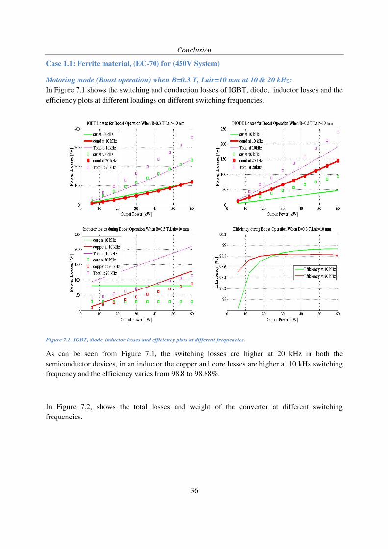
Case 1.1: Ferrite material, (EC-70) for (450V System)
Motoring mode (Boost operation) when B=0.3 T, Lair=10 mm at 10 & 20 kHz:
In Figure 7.1 shows the switching and conduction losses of IGBT, diode, inductor losses and the
efficiency plots at different loadings on different switching frequencies.
Figure 7.1. IGBT, diode, inductor losses and efficiency plots at different frequencies.
As can be seen from Figure 7.1, the switching losses are higher at 20 kHz in both the
semiconductor devices, in an inductor the copper and core losses are higher at 10 kHz switching
frequency and the efficiency varies from 98.8 to 98.88%.
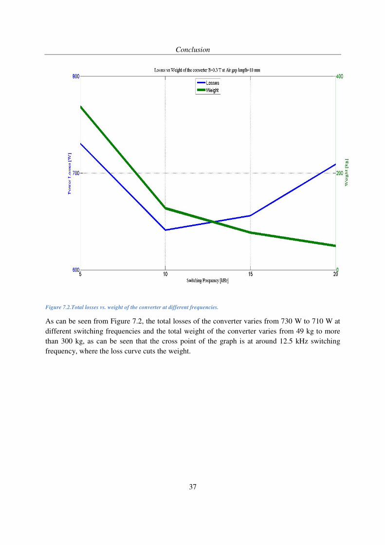
In Figure 7.2, shows the total losses and weight of the converter at different switching
frequencies.
Conclusion
37
Figure 7.2.Total losses vs. weight of the converter at different frequencies.
As can be seen from Figure 7.2, the total losses of the converter varies from 730 W to 710 W at
different switching frequencies and the total weight of the converter varies from 49 kg to more
than 300 kg, as can be seen that the cross point of the graph is at around 12.5 kHz switching
frequency, where the loss curve cuts the weight.
Conclusion
38
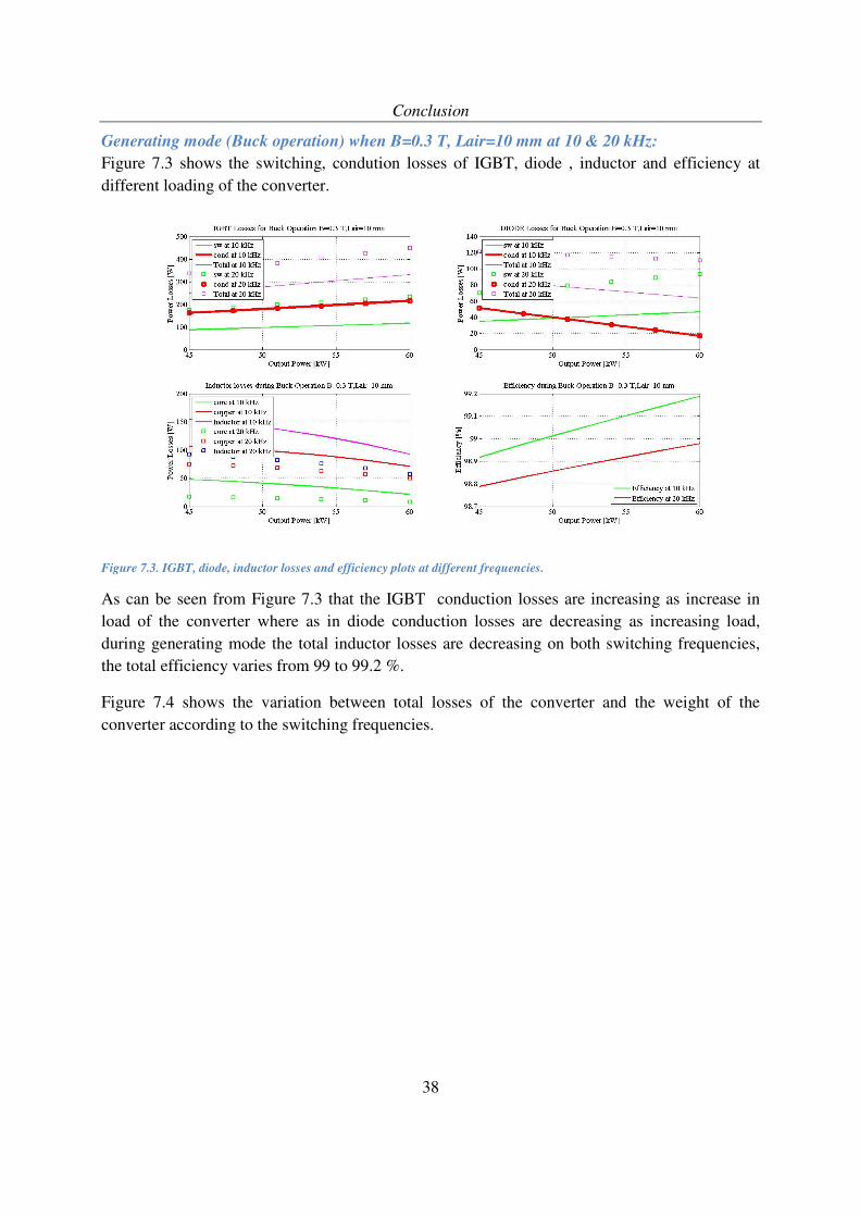
Generating mode (Buck operation) when B=0.3 T, Lair=10 mm at 10 & 20 kHz:
Figure 7.3 shows the switching, condution losses of IGBT, diode , inductor and efficiency at
different loading of the converter.
Figure 7.3. IGBT, diode, inductor losses and efficiency plots at different frequencies.
As can be seen from Figure 7.3 that the IGBT conduction losses are increasing as increase in
load of the converter where as in diode conduction losses are decreasing as increasing load,
during generating mode the total inductor losses are decreasing on both switching frequencies,
the total efficiency varies from 99 to 99.2 %.
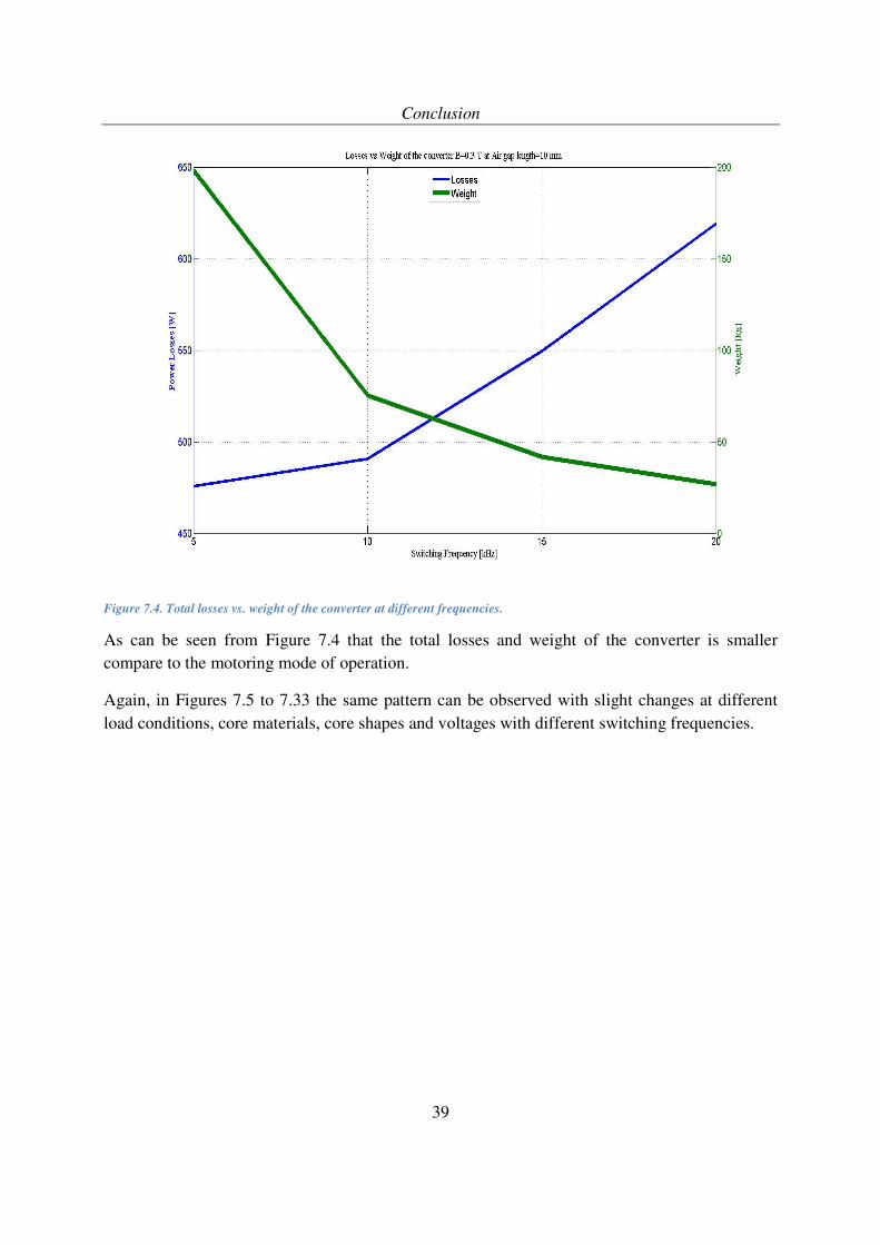
Figure 7.4 shows the variation between total losses of the converter and the weight of the
converter according to the switching frequencies.
Conclusion
39
Figure 7.4. Total losses vs. weight of the converter at different frequencies.
As can be seen from Figure 7.4 that the total losses and weight of the converter is smaller
compare to the motoring mode of operation.
Again, in Figures 7.5 to 7.33 the same pattern can be observed with slight changes at different
load conditions, core materials, core shapes and voltages with different switching frequencies.
Conclusion
40
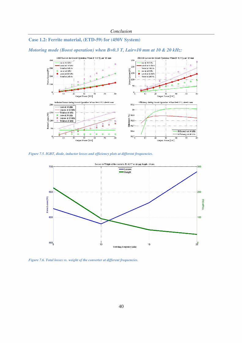
Case 1.2: Ferrite material, (ETD-59) for (450V System)
Motoring mode (Boost operation) when B=0.3 T, Lair=10 mm at 10 & 20 kHz:
Figure 7.5. IGBT, diode, inductor losses and efficiency plots at different frequencies.
Figure 7.6. Total losses vs. weight of the converter at different frequencies.
Conclusion
41
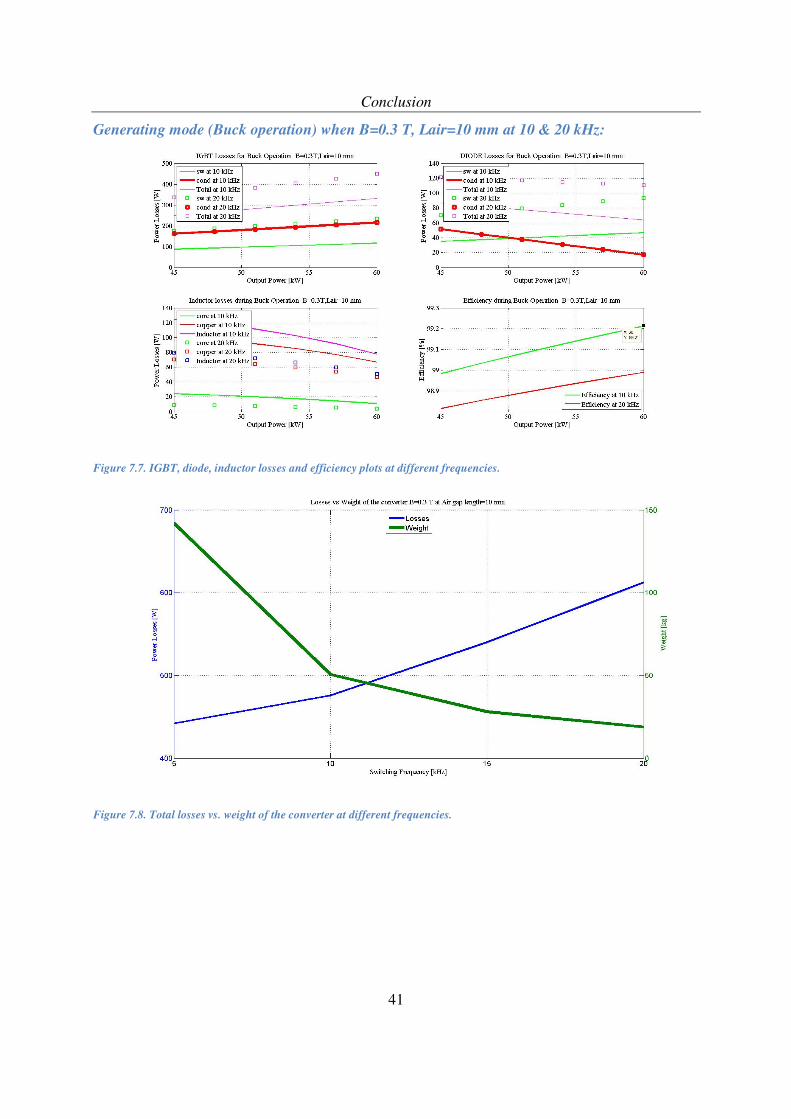
Generating mode (Buck operation) when B=0.3 T, Lair=10 mm at 10 & 20 kHz:
Figure 7.7. IGBT, diode, inductor losses and efficiency plots at different frequencies.
Figure 7.8. Total losses vs. weight of the converter at different frequencies.
Conclusion
42
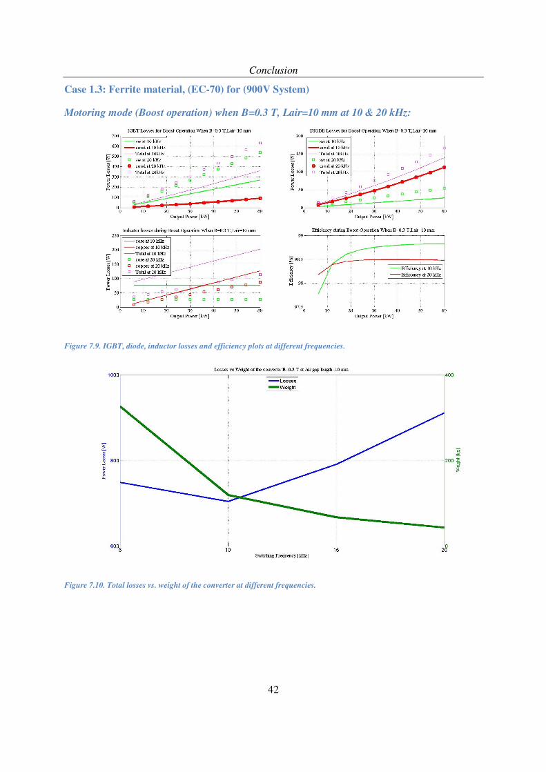
Case 1.3: Ferrite material, (EC-70) for (900V System)
Motoring mode (Boost operation) when B=0.3 T, Lair=10 mm at 10 & 20 kHz:
Figure 7.9. IGBT, diode, inductor losses and efficiency plots at different frequencies.
Figure 7.10. Total losses vs. weight of the converter at different frequencies.
Conclusion
43
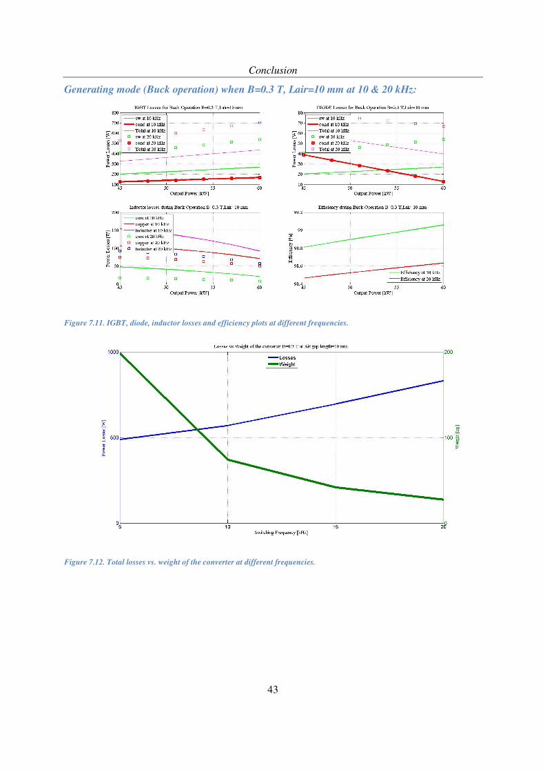
Generating mode (Buck operation) when B=0.3 T, Lair=10 mm at 10 & 20 kHz:
Figure 7.11. IGBT, diode, inductor losses and efficiency plots at different frequencies.
Figure 7.12. Total losses vs. weight of the converter at different frequencies.
Conclusion
44
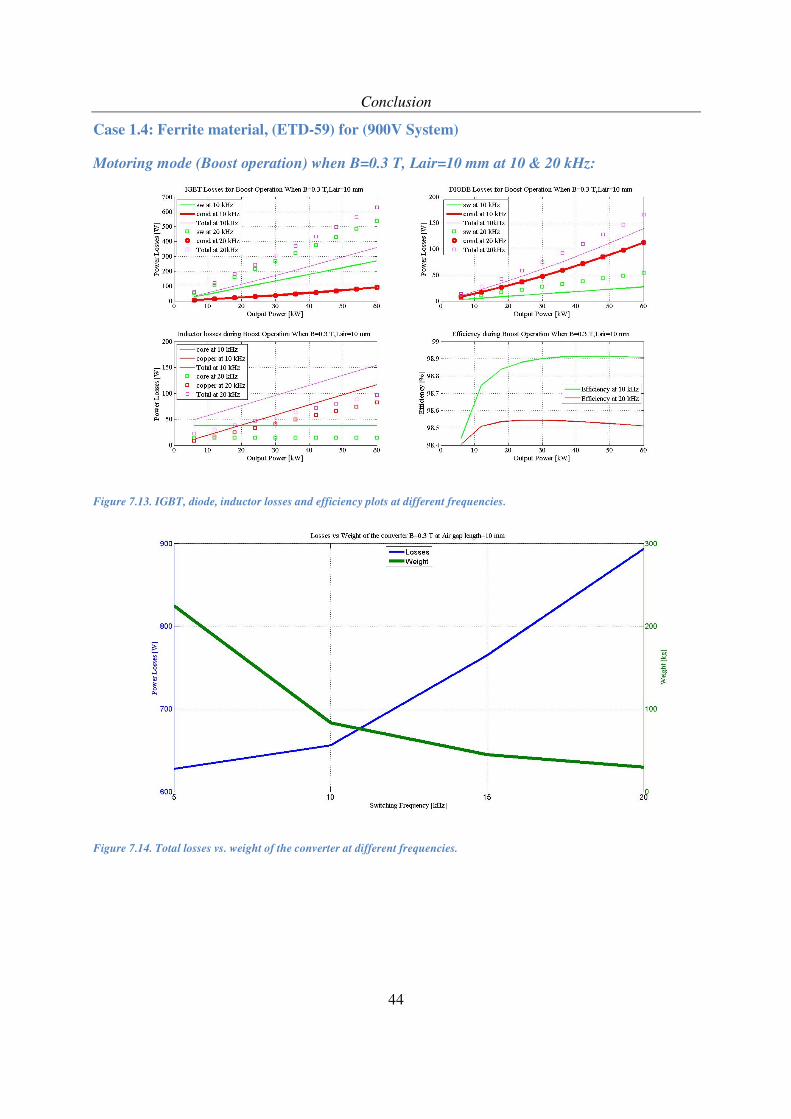
Case 1.4: Ferrite material, (ETD-59) for (900V System)
Motoring mode (Boost operation) when B=0.3 T, Lair=10 mm at 10 & 20 kHz:
Figure 7.13. IGBT, diode, inductor losses and efficiency plots at different frequencies.
Figure 7.14. Total losses vs. weight of the converter at different frequencies.
Conclusion
45
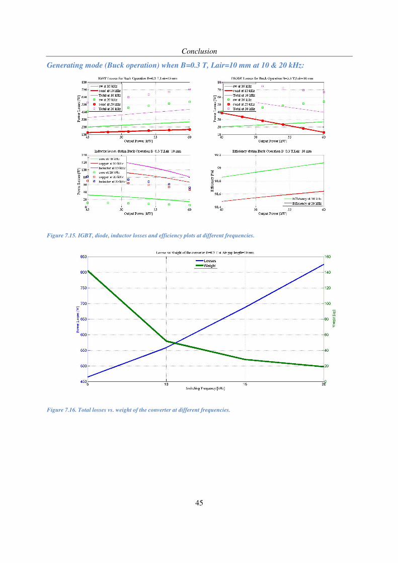
Generating mode (Buck operation) when B=0.3 T, Lair=10 mm at 10 & 20 kHz:
Figure 7.15. IGBT, diode, inductor losses and efficiency plots at different frequencies.
Figure 7.16. Total losses vs. weight of the converter at different frequencies.
Conclusion
46
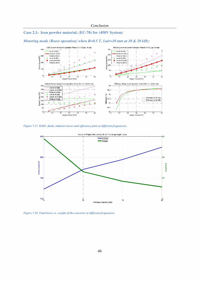
Case 2.1: Iron powder material, (EC-70) for (450V System)
Motoring mode (Boost operation) when B=0.5 T, Lair=10 mm at 10 & 20 kHz:
Figure 7.17. IGBT, diode, inductor losses and efficiency plots at different frequencies.
Figure 7.18. Total losses vs. weight of the converter at different frequencies.
Conclusion
47
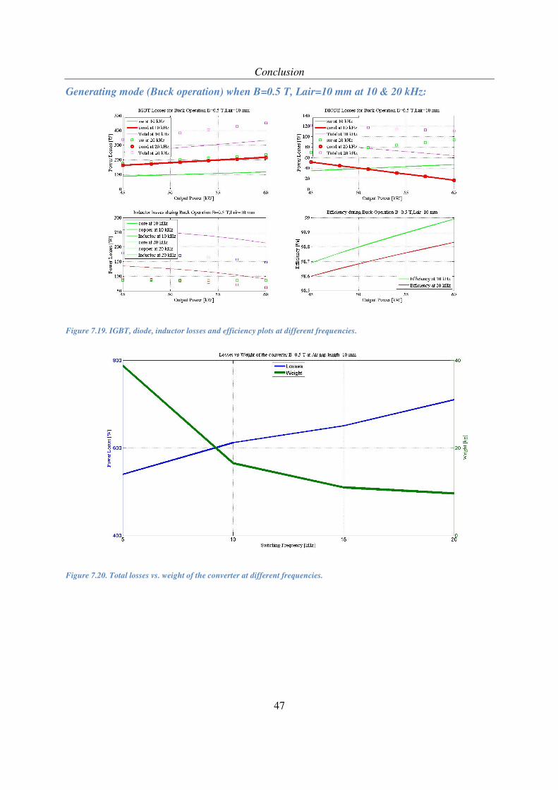
Generating mode (Buck operation) when B=0.5 T, Lair=10 mm at 10 & 20 kHz:
Figure 7.19. IGBT, diode, inductor losses and efficiency plots at different frequencies.
Figure 7.20. Total losses vs. weight of the converter at different frequencies.
Conclusion
48
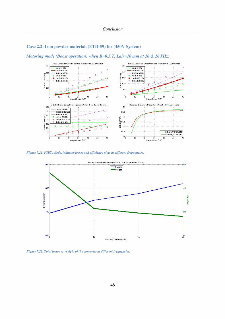
Case 2.2: Iron powder material, (ETD-59) for (450V System)
Motoring mode (Boost operation) when B=0.5 T, Lair=10 mm at 10 & 20 kHz:
Figure 7.21. IGBT, diode, inductor losses and efficiency plots at different frequencies.
Figure 7.22. Total losses vs. weight of the converter at different frequencies.
Conclusion
49
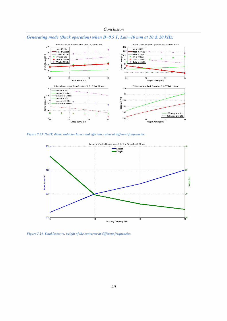
Generating mode (Buck operation) when B=0.5 T, Lair=10 mm at 10 & 20 kHz:
Figure 7.23. IGBT, diode, inductor losses and efficiency plots at different frequencies.
Figure 7.24. Total losses vs. weight of the converter at different frequencies.
Conclusion
50
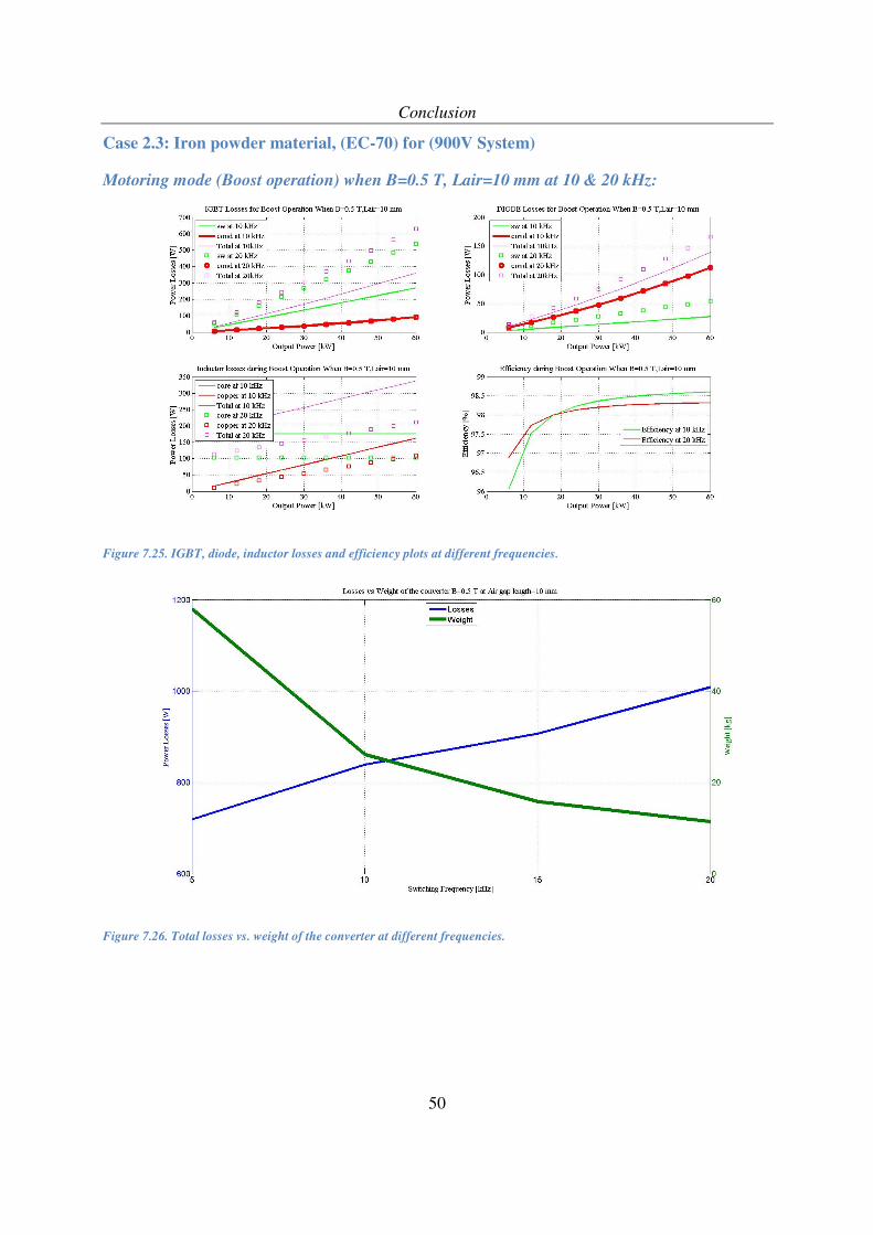
Case 2.3: Iron powder material, (EC-70) for (900V System)
Motoring mode (Boost operation) when B=0.5 T, Lair=10 mm at 10 & 20 kHz:
Figure 7.25. IGBT, diode, inductor losses and efficiency plots at different frequencies.
Figure 7.26. Total losses vs. weight of the converter at different frequencies.
Conclusion
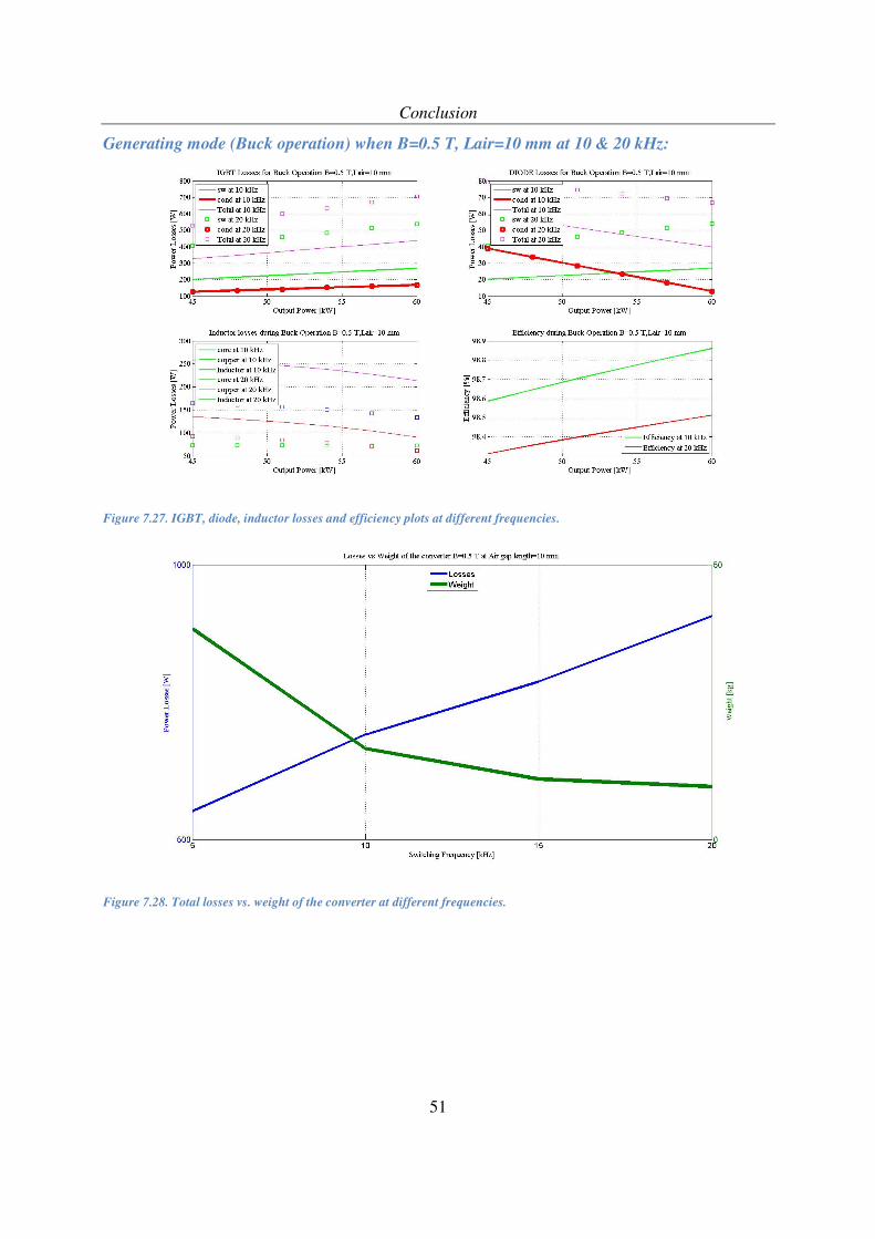
51
Generating mode (Buck operation) when B=0.5 T, Lair=10 mm at 10 & 20 kHz:
Figure 7.27. IGBT, diode, inductor losses and efficiency plots at different frequencies.
Figure 7.28. Total losses vs. weight of the converter at different frequencies.
Conclusion
52
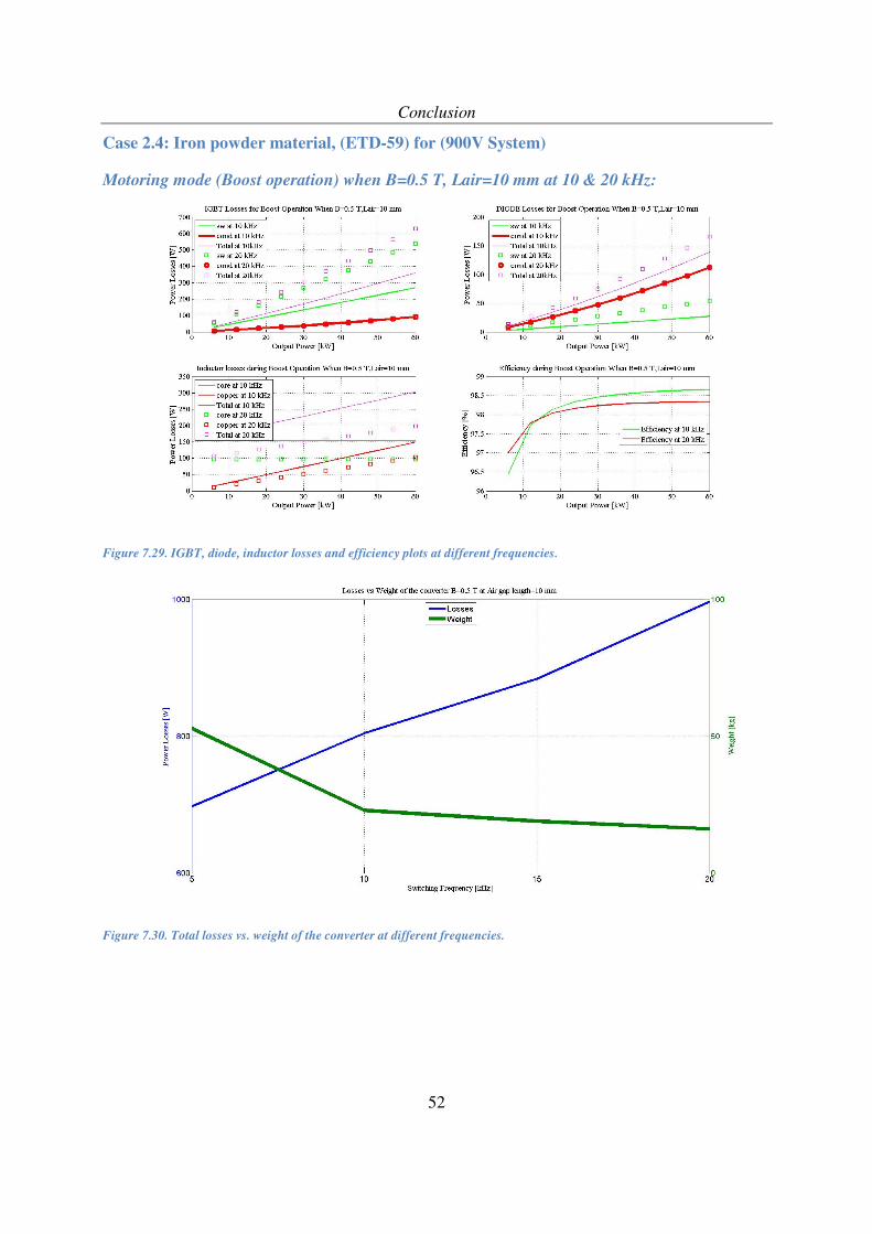
Case 2.4: Iron powder material, (ETD-59) for (900V System)
Motoring mode (Boost operation) when B=0.5 T, Lair=10 mm at 10 & 20 kHz:
Figure 7.29. IGBT, diode, inductor losses and efficiency plots at different frequencies.
Figure 7.30. Total losses vs. weight of the converter at different frequencies.
Conclusion
53
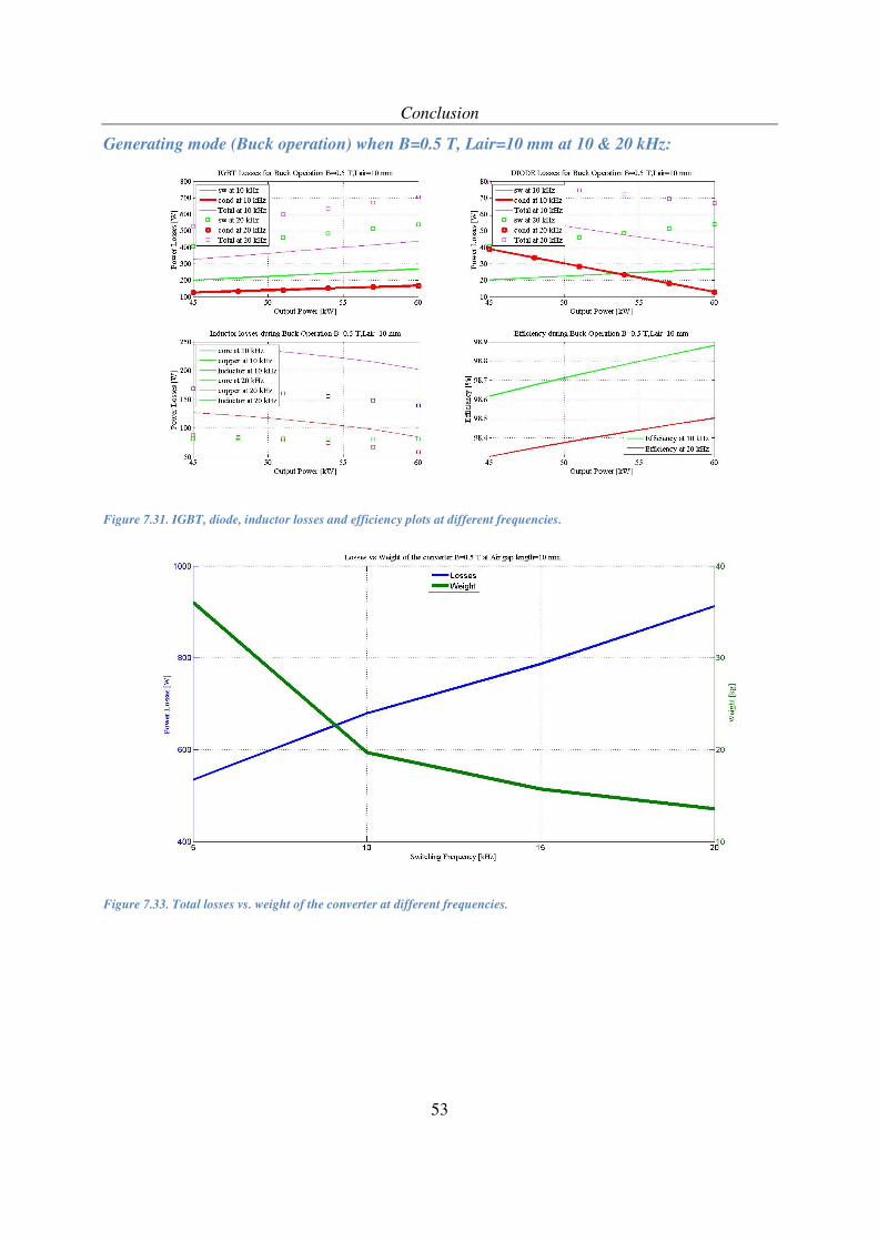
Generating mode (Buck operation) when B=0.5 T, Lair=10 mm at 10 & 20 kHz:
Figure 7.31. IGBT, diode, inductor losses and efficiency plots at different frequencies.
Figure 7.33. Total losses vs. weight of the converter at different frequencies.
Conclusion
54
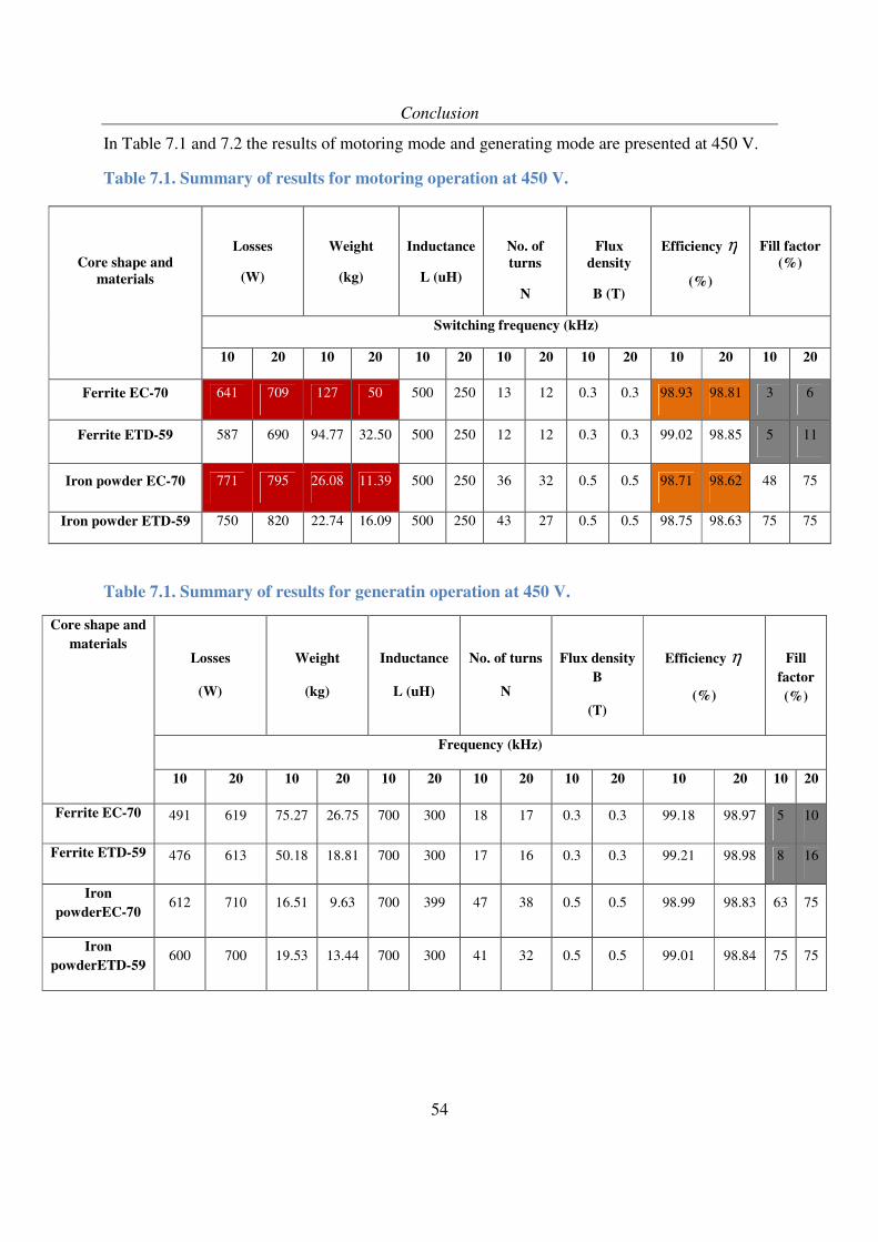
In Table 7.1 and 7.2 the results of motoring mode and generating mode are presented at 450 V.
Table 7.1. Summary of results for motoring operation at 450 V.
Table 7.1. Summary of results for generatin operation at 450 V.
Core shape and
materials
Losses
(W)
Weight
(kg)
Inductance
L (uH)
No. of turns
N
Flux density
B
(T)
Efficiency η
(%)
Fill
factor
(%)
Frequency (kHz)
10 20 10 20 10 20 10 20 10 20 10 20 10 20
Ferrite EC-70 491 619 75.27 26.75 700 300 18 17 0.3 0.3 99.18 98.97 5 10
Ferrite ETD-59 476 613 50.18 18.81 700 300 17 16 0.3 0.3 99.21 98.98 8 16
Iron
powderEC-70 612 710 16.51 9.63 700 399 47 38 0.5 0.5 98.99 98.83 63 75
Iron
powderETD-59 600 700 19.53 13.44 700 300 41 32 0.5 0.5 99.01 98.84 75 75
Core shape and
materials
Losses
(W)
Weight
(kg)
Inductance
L (uH)
No. of
turns
N
Flux
density
B (T)
Efficiency η
(%)
Fill factor
(%)
Switching frequency (kHz)
10 20 10 20 10 20 10 20 10 20 10 20 10 20
Ferrite EC-70 641 709 127 50 500 250 13 12 0.3 0.3 98.93 98.81 3 6
Ferrite ETD-59 587 690 94.77 32.50 500 250 12 12 0.3 0.3 99.02 98.85 5 11
Iron powder EC-70 771 795 26.08 11.39 500 250 36 32 0.5 0.5 98.71 98.62 48 75
Iron powder ETD-59 750 820 22.74 16.09 500 250 43 27 0.5 0.5 98.75 98.63 75 75
Conclusion
55
The summary of results from both motoring and generating mode of operation taking into
account at 450 V system and show the losses, weight, inductance, number of turns peak flux
density, efficiency, fill factor with different core material, core shapes, at different switching
frequencies.
And , the red and orange marked in Table 7.1 show how the losses, weight and efficiency varies
according to different parameters.
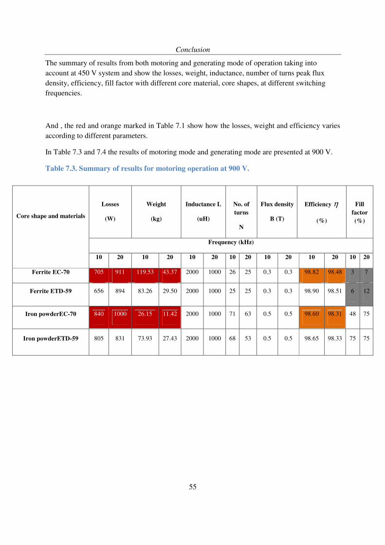
In Table 7.3 and 7.4 the results of motoring mode and generating mode are presented at 900 V.
Table 7.3. Summary of results for motoring operation at 900 V.
Core shape and materials
Losses
(W)
Weight
(kg)
Inductance L
(uH)
No. of
turns
N
Flux density
B (T)
Efficiency η
(%)
Fill
factor
(%)
Frequency (kHz)
10 20 10 20 10 20 10 20 10 20 10 20 10 20
Ferrite EC-70 705 911 119.53 43.37 2000 1000 26 25 0.3 0.3 98.82 98.48 3 7
Ferrite ETD-59 656 894 83.26 29.50 2000 1000 25 25 0.3 0.3 98.90 98.51 6 12
Iron powderEC-70 840 1000 26.15 11.42 2000 1000 71 63 0.5 0.5 98.60 98.31 48 75
Iron powderETD-59 805 831 73.93 27.43 2000 1000 68 53 0.5 0.5 98.65 98.33 75 75
Conclusion
56
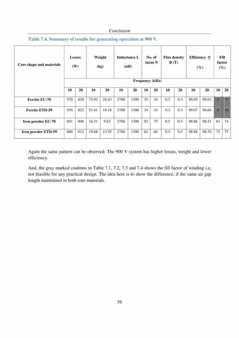
Table 7.4. Summary of results for generating operation at 900 V.
Core shape and materials
Losses
(W)
Weight
(kg)
Inductance L
(uH)
No. of
turns N
Flux density
B (T)
Efficiency η
(%)
Fill
factor
(%)
Frequency (kHz)
10 20 10 20 10 20 10 20 10 20 10 20 10 20
Ferrite EC-70 570 830 73.93 24.43 2700 1300 35 34 0.3 0.3 99.05 98.63 5 9
Ferrite ETD-59 559 825 51.61 18.18 2700 1300 34 34 0.3 0.3 99.07 98.64 8 16
Iron powder EC-70 691 906 16.51 9.63 2700 1300 92 75 0.5 0.5 98.86 98.51 63 74
Iron powder ETD-59 680 912 19.68 13.55 2700 1300 82 64 0.5 0.5 98.88 98.70 75 75
Again the same pattern can be observed: The 900 V system has higher losses, weight and lower
efficiency.
And, the gray marked coulmns in Table 7.1, 7.2, 7.3 and 7.4 shows the fill factor of winding i.e,
not feasible for any practical design. The idea here is to show the difference, if the same air gap
length maintained in both core materials.
Conclusion
57
8 CONCLUSION
In this thesis, DC-DC converter is investigated with different core materials, core shapes,
different voltage levels (450 and 900V) and at two different frequencies (10 and 20 kHz) for a
EV/BEV/HEV.
• The efficiency of the converter is higher for a ferrite material when the ETD-59 core
shape is used as compared with EC-70 core shape is used for both voltage levels.
• The weight of the converter with ferrite material is lower for the ETD-59 core shape for
both voltage systems.
• The 450 V system is better than 900 V system with ferrite core material.
• The efficiency of the converter is higher for iron powder material when the ETD-59 core
shape is used as compared EC-70 core shape for both voltage levels.
• The weight of the converter with ferrite material is lower for the EC-70 core shape for
both voltage systems.
• The 450 V system is better than the 900 V system with iron powder core material.
• For lower airgap lengths the fill factor is not feasible with ferrite core material.
Hence the design of DC-DC converter with the EC-70 core shape, iron powder material, 450 V
system at 20 kHz is better.
The future work is to implement the converter in Matlab Simulink and more over, to validate
with the practical design.

Conclusion
58
References
59
REFERENCES
[1] Mi, C., Peng, F.Z., Kelly, K.J., O'Keefe, M. and Hassani, V. (2008), `Topology, design,
analysis and thermal management of power electronics for hybrid electric vehicle
applications', Int. J. Electric and Hybrid Vehicles. Vol. 1, No. 3, pp.276±294.
[2] Edition 2009-01-29, Published by Infineon Technologies AG, Am Campeon 1-12,
85579 Neubiberg, Germany, © Infineon Technologies AG 2006.
[3] http://en.wikipedia.org/wiki/Lithium-ion_battery
[4] David Linden, Thomas B. Reddy (ed). Handbook Of Batteries 3rd Edition. McGraw-Hill,
New York, 2002 ISBN 0-07-135978-8 chapter 35
[5] http://www.mitsubishi-
otors.com/corporate/about_us/technology/review/e/pdf/2003/15E_10.pdf
[6] Mohan, Undeland, Robbins; ‘Power Electronics Converters, applications and design,
media enhanced third edition, John Wiley & sons, Inc., pp. 760-767
[7] http://igbt.cn/admin/productfile/BSM300GB60DLC.pdf
[8] http://www.hipih.com/SMC/datasheet/SMC_gWBPuycesVEfh.htm