marvell - storage - 88sm9705 functional specifications · page -iii update added automotive grade...
TRANSCRIPT
Doc No. MV-S109142-00 Rev. A
June 12, 2015
Document Classification: ProprietaryMarvell. Moving Forward Faster
88SM9705 SATA 6.0 Gbps: 1-to-5 Port Multiplier
Preliminary Specifications
88SM9705 SATA 6.0 Gbps: 1-to-5 Port MultiplierPreliminary Specifications
No part of this document may be reproduced or transmitted in any form or by any means, electronic or mechanical, including photocopying and recording, for any purpose, without the express written permission of Marvell. Marvell retains the right to make changes to this document at any time, without notice. Marvell makes no warranty of any kind, expressed or implied, with regard to any information contained in this document, including, but not limited to, the implied warranties of merchantability or fitness for any particular purpose. Further, Marvell does not warrant the accuracy or completeness of the information, text, graphics, or other items contained within this document. Marvell products are not designed for use in life-support equipment or applications that would cause a life-threatening situation if any such products failed. Do not use Marvell products in these types of equipment or applications. With respect to the products described herein, the user or recipient, in the absence of appropriate U.S. government authorization, agrees: 1) Not to re-export or release any such information consisting of technology, software or source code controlled for national security reasons by the U.S. Export Control Regulations ("EAR"), to a national of EAR Country Groups D:1 or E:2; 2) Not to export the direct product of such technology or such software, to EAR Country Groups D:1 or E:2, if such technology or software and direct products thereof are controlled for national security reasons by the EAR; and, 3) In the case of technology controlled for national security reasons under the EAR where the direct product of the technology is a complete plant or component of a plant, not to export to EAR Country Groups D:1 or E:2 the direct product of the plant or major component thereof, if such direct product is controlled for national security reasons by the EAR, or is subject to controls under the U.S. Munitions List ("USML"). At all times hereunder, the recipient of any such information agrees that they shall be deemed to have manually signed this document in connection with their receipt of any such information.
Copyright © 1999–2015. Marvell International Ltd. All rights reserved. Alaska, ARMADA, Avanta, Avastar, CarrierSpan, Kinoma, Link Street, LinkCrypt, Marvell logo, Marvell, Moving Forward Faster, Marvell Smart, PISC, Prestera, Qdeo, QDEO logo, QuietVideo, Virtual Cable Tester, The World as YOU See It, Vmeta, Xelerated, and Yukon are registered trademarks of Marvell or its affiliates. G.now, HyperDuo, Kirkwood, and Wirespeed by Design are trademarks of Marvell or its affiliates.
Patent(s) Pending—Products identified in this document may be covered by one or more Marvell patents and/or patent applications.
For more information, visit our website at: www.marvell.com
ii
Copyright © 2015 Marvell Doc No. MV-S109142-00 Rev. AJune 12, 2015 Document Classification: Proprietary

Ordering Information
ORDERING INFORMATION
Ordering Part Numbers and Package Markings
The following figure shows the ordering part numbering scheme for the 88SM9705 part. For complete ordering information, contact your Marvell FAE or sales representative.
Figure 0-1 Sample Ordering Part Number
The standard ordering part numbers for the respective solutions are indicated in the following table.
The next figure shows a typical Marvell package marking.
Figure 0-2 88SM9705 Package Marking and Pin 1 Location
Note: The above drawing is not drawn to scale. The location of markings is approximate. Add-on marks are not represented. Flip chips vary widely in their markings and flip chip examples are not shown here. For flip chips, the markings may be omitted per customer requirement.
Ordering Part Numbers
Part Number Description
88SM9705A0-NNR2C000 84-Pin 10 x 10 QFN Package, SATA 6.0 Gbps, One-to-Five Port Multiplier
88SM9705A0-NNR2I000 84-Pin 10 x 10 Industrial Grade QFN Package, SATA 6.0 Gbps, One-to-Five Port Multiplier
88SM9705A0-NNR2A000 84-Pin 10 x 10 Automotive Grade QFN Package, SATA 6.0 Gbps, One-to-Five Port Multiplier
Part Number
Product Revision
Custom Code
Custom Code(optional )
88XXXXX - XX - XXX - C000 - XXXX
Temperature CodeC = CommercialI = Industrial
Environmental Code + = RoHS 0/6–= RoHS 5/61 = RoHS 6/62 = Green)
Package Code3-character
alphabetic code such as BCC, TEH
Custom Code
Extended Part Number
YYWW xx@Country of Origin
Part number, package code, environmental code eXXXXX = Part number AAA = Package codee = Environmental code (+ = RoHS 0/6, no code = RoHS 5/6, 1 = RoHS 6/6, 2 = Green)
Country of origin(contained in the mold ID ormarked as the last line onthe package)
Pin 1 location
Marvell Logo
Lot Number88XXXXX-AAAe
Date code, custom code, assembly plant codeYYWW = Date code (YY = year, WW = Work Week)xx = Custom code or die revision@ = Assembly plant code
iii
Copyright © 2015 Marvell Doc No. MV-S109142-00 Rev. AJune 12, 2015 Document Classification: Proprietary

88SM9705 SATA 6.0 Gbps: 1-to-5 Port MultiplierPreliminary Specifications
THIS PAGE LEFT INTENTIONALLY BLANK
iv
Copyright © 2015 Marvell Doc No. MV-S109142-00 Rev. AJune 12, 2015 Document Classification: Proprietary
Change History
CHANGE HISTORY
The following table identifies the document change history for Rev. A.
Document Changes *
* The type of change is categorized as: Parameter, Revision, or Update. A Parameter change is a change to a spec value, a Revision change is one that originates from the chip Revision Notice, and an Update change includes all other document updates.
Location Type Description Date
Page -iii Update Added automotive grade part number 88SM9705A0-NNR2A000 to the Ordering Part Numbers table.
May 6, 2015
Global Update Updated section 4.1, Board Schematic Example as follows:
• Replaced schematic diagrams with updated versions.
April 7, 2015
Global Update Added an introduction sentence to all tables in the document. September 26, 2013
Global Update Added GPIO registers. October 21, 2014
Page 2-2 Update Removed the following bullet item in section 2.1, General:
“Full scan for high-production test coverage and PHY self-test.”
October 21, 2014
Page 2-3 Update Added the following bullet item for 2.2, Functional: “Supports SATA Port Multiplier Rev. 1.2.”
February 28,2013
Page 9-5 Update Added section 9.5, Thermal Data. September 14 2014
Page 8-13 Parameter Corrected the default value of PORT_NUM (R002h [3:0]) from 5h to Vh. February 26, 2013
Page 8-42 Update Updated description for GPIO[19]_SRC_SEL (R3E4h [9:5]).
March 27, 2015
Page 8-42 Update Updated description for GPIO[18]_OUTPUT_SRC_SEL (R3E4h [4:0]).
March 27, 2015
v
Copyright © 2015 Marvell Doc No. MV-S109142-00 Rev. AJune 12, 2015 Document Classification: Proprietary

88SM9705 SATA 6.0 Gbps: 1-to-5 Port MultiplierPreliminary Specifications
THIS PAGE LEFT INTENTIONALLY BLANK
vi
Copyright © 2015 Marvell Doc No. MV-S109142-00 Rev. AJune 12, 2015 Document Classification: Proprietary
Contents
CONTENTS
1 OVERVIEW ........................................................................................................................................................ 1-1
2 FEATURES ........................................................................................................................................................ 2-1
2.1 GENERAL .................................................................................................................................................. 2-2
2.2 FUNCTIONAL .............................................................................................................................................. 2-3
3 PACKAGE ......................................................................................................................................................... 3-1
3.1 PACKAGE PIN-OUT .................................................................................................................................... 3-2
3.2 PACKAGE DIMENSIONS ............................................................................................................................... 3-3
3.3 PIN DESCRIPTIONS .................................................................................................................................... 3-53.3.1 Pin Type Definitions .................................................................................................................. 3-53.3.2 Pin List ...................................................................................................................................... 3-5
4 LAYOUT GUIDELINES ...................................................................................................................................... 4-1
4.1 BOARD SCHEMATIC EXAMPLE .................................................................................................................... 4-2
4.2 LAYER STACK-UP ...................................................................................................................................... 4-24.2.1 Layer 1–Topside, Parts, Slow and High Speed Signal Routes, and Power Routes .................. 4-24.2.2 Layer 2–Solid Ground Plane ..................................................................................................... 4-34.2.3 Layer 3–Power Plane ................................................................................................................ 4-34.2.4 Layer 4–Bottom Layer, Slow and High-Speed Signal Routes, and Power Routes ................... 4-3
4.3 POWER SUPPLY ........................................................................................................................................ 4-34.3.1 VDD Power (1.0V) ..................................................................................................................... 4-34.3.2 Analog Power Supply (1.8V) ..................................................................................................... 4-44.3.3 VDDIO Power (3.3V) ................................................................................................................. 4-44.3.4 Power-on-Reset Timing Requirement ....................................................................................... 4-44.3.5 Bias Current Resistor (RSET) ................................................................................................... 4-4
4.4 PCB TRACE ROUTING ............................................................................................................................... 4-4
4.5 RECOMMENDED LAYOUT ............................................................................................................................ 4-4
5 GENERAL PURPOSE I/O PORT INTERFACE ................................................................................................. 5-1
5.1 OVERVIEW ................................................................................................................................................. 5-2
5.2 GPIO NORMAL MODE ................................................................................................................................ 5-3
5.3 GPIO SAMPLE-AT-RESET PINS .................................................................................................................. 5-5
6 UART INTERFACE ............................................................................................................................................ 6-1
6.1 UART INTERFACE OVERVIEW .................................................................................................................... 6-2
6.2 UART INTERFACE TIMING .......................................................................................................................... 6-3
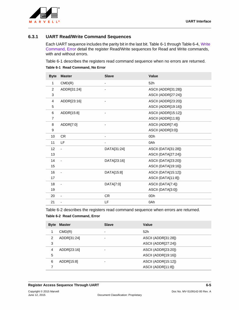
6.3 REGISTER ACCESS SEQUENCE THROUGH UART ........................................................................................ 6-46.3.1 UART Read/Write Command Sequences ................................................................................. 6-5
7 PORTS ............................................................................................................................................................... 7-1
7.1 PM_PORT FIELD ...................................................................................................................................... 7-2
7.2 CONTROL PORTS ....................................................................................................................................... 7-2
7.3 CASCADING ............................................................................................................................................... 7-3
vii
Copyright © 2015 Marvell Doc No. MV-S109142-00 Rev. AJune 12, 2015 Document Classification: Proprietary
88SM9705 SATA 6.0 Gbps: 1-to-5 Port MultiplierPreliminary Specifications
8 REGISTERS ....................................................................................................................................................... 8-1
8.1 REGISTER SUMMARY ................................................................................................................................. 8-28.1.1 Register Access from Host and UART ...................................................................................... 8-28.1.2 General Status and Control Registers ...................................................................................... 8-68.1.3 Vendor-Specific Port Multiplier Control Registers .................................................................... 8-68.1.4 Host Port PHY Event Counter Registers ................................................................................... 8-68.1.5 General Purpose Input/Output (GPIO) Registers ...................................................................... 8-78.1.6 SATA PHY and Link Registers .................................................................................................. 8-78.1.7 Device Port PHY Event Counter Registers ............................................................................... 8-8
8.2 REGISTER MAP SUMMARY ......................................................................................................................... 8-8
8.3 REGISTER DESCRIPTION .......................................................................................................................... 8-128.3.1 General Status and Control Registers .................................................................................... 8-128.3.2 Vendor-Specific Port Multiplier Control Registers ................................................................... 8-178.3.3 Host Port PHY Event Counter Registers ................................................................................. 8-258.3.4 General Purpose Input/Output (GPIO) Registers .................................................................... 8-258.3.5 SATA PHY and Link Registers ................................................................................................ 8-478.3.6 Device Port PHY Event Counter Registers ............................................................................. 8-51
9 ELECTRICAL SPECIFICATIONS ...................................................................................................................... 9-1
9.1 ABSOLUTE MAXIMUM RATINGS ................................................................................................................... 9-2
9.2 POWER REQUIREMENTS ............................................................................................................................. 9-2
9.3 RECOMMENDED/TYPICAL OPERATING CONDITIONS .................................................................................... 9-3
9.4 DC CHARACTERISTICS .............................................................................................................................. 9-4
9.5 THERMAL DATA ......................................................................................................................................... 9-5
viii
Copyright © 2015 Marvell Doc No. MV-S109142-00 Rev. AJune 12, 2015 Document Classification: Proprietary
Overview
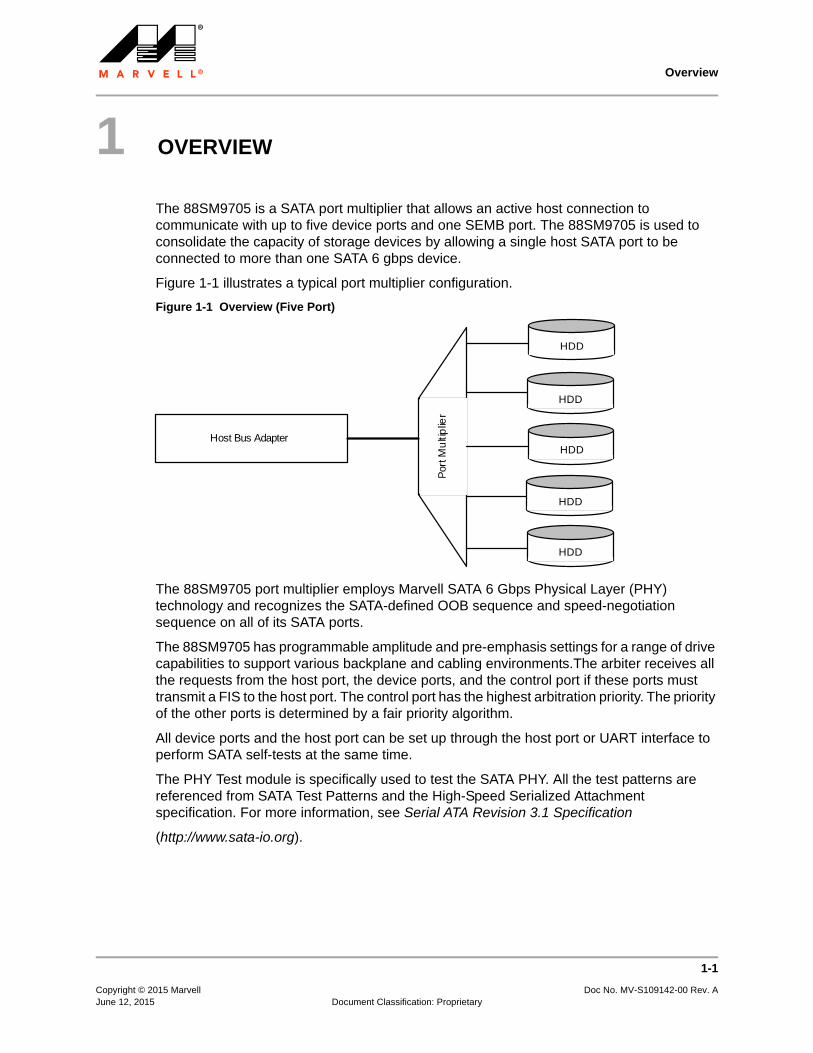
1 OVERVIEW
The 88SM9705 is a SATA port multiplier that allows an active host connection to communicate with up to five device ports and one SEMB port. The 88SM9705 is used to consolidate the capacity of storage devices by allowing a single host SATA port to be connected to more than one SATA 6 gbps device.
Figure 1-1 illustrates a typical port multiplier configuration.
Figure 1-1 Overview (Five Port)
The 88SM9705 port multiplier employs Marvell SATA 6 Gbps Physical Layer (PHY) technology and recognizes the SATA-defined OOB sequence and speed-negotiation sequence on all of its SATA ports.
The 88SM9705 has programmable amplitude and pre-emphasis settings for a range of drive capabilities to support various backplane and cabling environments.The arbiter receives all the requests from the host port, the device ports, and the control port if these ports must transmit a FIS to the host port. The control port has the highest arbitration priority. The priority of the other ports is determined by a fair priority algorithm.
All device ports and the host port can be set up through the host port or UART interface to perform SATA self-tests at the same time.
The PHY Test module is specifically used to test the SATA PHY. All the test patterns are referenced from SATA Test Patterns and the High-Speed Serialized Attachment specification. For more information, see Serial ATA Revision 3.1 Specification
(http://www.sata-io.org).
HDD
Host Bus Adapter
HDD
HDD
HDD
HDD
Por
t Mu
ltip
lier
1-1
Copyright © 2015 Marvell Doc No. MV-S109142-00 Rev. AJune 12, 2015 Document Classification: Proprietary
88SM9705 SATA 6.0 Gbps: 1-to-5 Port MultiplierPreliminary Specifications
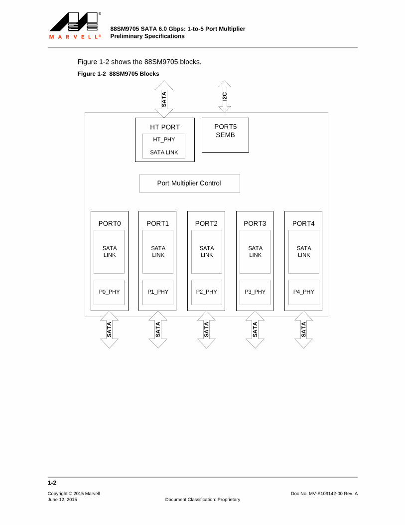
Figure 1-2 shows the 88SM9705 blocks.
Figure 1-2 88SM9705 Blocks
SATALINK
Port Multiplier Control
P0_PHY
HT_PHY
SATA LINK
PORT0
SA
TA
PORT5SEMB
I2C
SA
TA
HT PORT
PORT1 PORT2 PORT3 PORT4
SA
TA
SA
TA
SA
TA
SA
TA
SATALINK
SATALINK
SATALINK
SATALINK
P1_PHY P2_PHY P3_PHY P4_PHY
1-2
Copyright © 2015 Marvell Doc No. MV-S109142-00 Rev. AJune 12, 2015 Document Classification: Proprietary
Features
2 FEATURES
This chapter contains the following sections:
General
Functional
2-1
Copyright © 2015 Marvell Doc No. MV-S109142-00 Rev. AJune 12, 2015 Document Classification: Proprietary
88SM9705 SATA 6.0 Gbps: 1-to-5 Port MultiplierPreliminary Specifications
2.1 General
55 nm CMOS technology.
Supports Serial ATA Revision 3.1 Specification, with communication speeds of 1.5 Gbps, 3 Gbps, and 6 Gbps on host and device ports.
1.0V, 1.8V, and 3.3V power.
84-pin QFN ePad package.
PHY test mode.
One host port.
Five device
Supports 25 MHz reference clock.
2-2 General
Copyright © 2015 Marvell Doc No. MV-S109142-00 Rev. AJune 12, 2015 Document Classification: Proprietary
Features
2.2 Functional
115200 bps UART access.
Spread-spectrum clocking transmission.
SATA BIST over host and device links.
Asynchronous notification.
NOP command to select PM port field (Marvell Specific Mode, optional).SPI interface for internal register programming.
Supports SATA Port Multiplier Rev. 1.2.
Functional 2-3
Copyright © 2015 Marvell Doc No. MV-S109142-00 Rev. AJune 12, 2015 Document Classification: Proprietary
88SM9705 SATA 6.0 Gbps: 1-to-5 Port MultiplierPreliminary Specifications
THIS PAGE LEFT INTENTIONALLY BLANK
2-4 Functional
Copyright © 2015 Marvell Doc No. MV-S109142-00 Rev. AJune 12, 2015 Document Classification: Proprietary
Package
3 PACKAGE
This chapter contains the following sections:
Package Pin-Out
Package Dimensions
Pin Descriptions
3-1
Copyright © 2015 Marvell Doc No. MV-S109142-00 Rev. AJune 12, 2015 Document Classification: Proprietary
88SM9705 SATA 6.0 Gbps: 1-to-5 Port MultiplierPreliminary Specifications
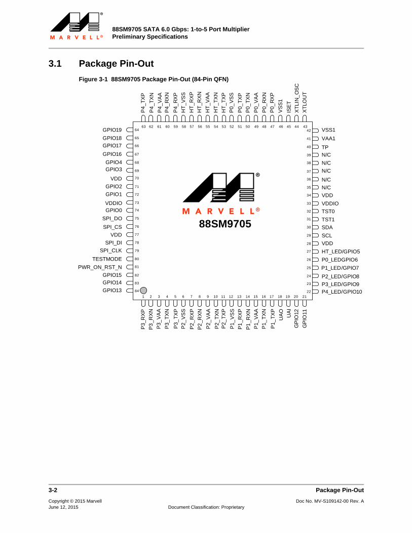
3.1 Package Pin-Out
Figure 3-1 88SM9705 Package Pin-Out (84-Pin QFN)
64
66
65
67
69
68
70
72
71
73
75
74
76
78
77
79
82
81
80
84
83
1 2 3 4 5 6 7 8 9 10 11 12 1814 15 16 1713 19 20 21
22
23
24
25
26
27
28
29
30
31
32
33
34
35
36
37
38
39
40
41
4263 5762 61 60 59 58 56 5455 53 52 51 50 49 48 47 46 45 44 43
P4
_TX
P
P4
_TX
N
P4
_VA
AP
4_R
XN
P4_
RX
P
HT
_VS
S
HT
_RX
P
HT
_RX
N
HT
_VA
A
HT
_TX
N
HT
_TX
P
TP
VSS1
VAA1
XT
LOU
T
XT
LIN
_O
SC
ISE
T
N/C
N/C
N/C
N/C
VDD
VDDIO
TST0
TST1
SDA
SCL
VDD
HT_LED/GPIO5
P0_LEDGPIO6
P1_LED/GPIO7
P2_LED/GPIO8
P3_LED/GPIO9
P4_LED/GPIO10
P3_
RX
P
P3
_RX
N
P3_
VA
A
P3_
TX
N
P3_
TX
P
P2_
VS
S
P2_
RX
P
P2
_RX
N
P2_
VA
A
P2_
TX
NP
2_T
XP
P1_
VS
S
P1
_RX
P
P1
_RX
N
P1_
VA
A
P1_
TX
N
P1_
TX
P
UA
O
UA
I
GP
IO12
GP
IO11
GPIO19
GPIO18
GPIO17
GPIO16
GPIO4GPIO3
GPIO2
VDD
GPIO1
VDDIOGPIO0
VDD
SPI_DO
SPI_CLK
SPI_CS
SPI_DI
TESTMODE
PWR_ON_RST_N
GPIO15
GPIO14
GPIO13
88SM9705
N/C
VS
S1
P0_
RX
P
P0_
RX
N
P0_
VA
A
P0_
TX
N
P0_
TX
P
P0_
VS
S
3-2 Package Pin-Out
Copyright © 2015 Marvell Doc No. MV-S109142-00 Rev. AJune 12, 2015 Document Classification: Proprietary
Package
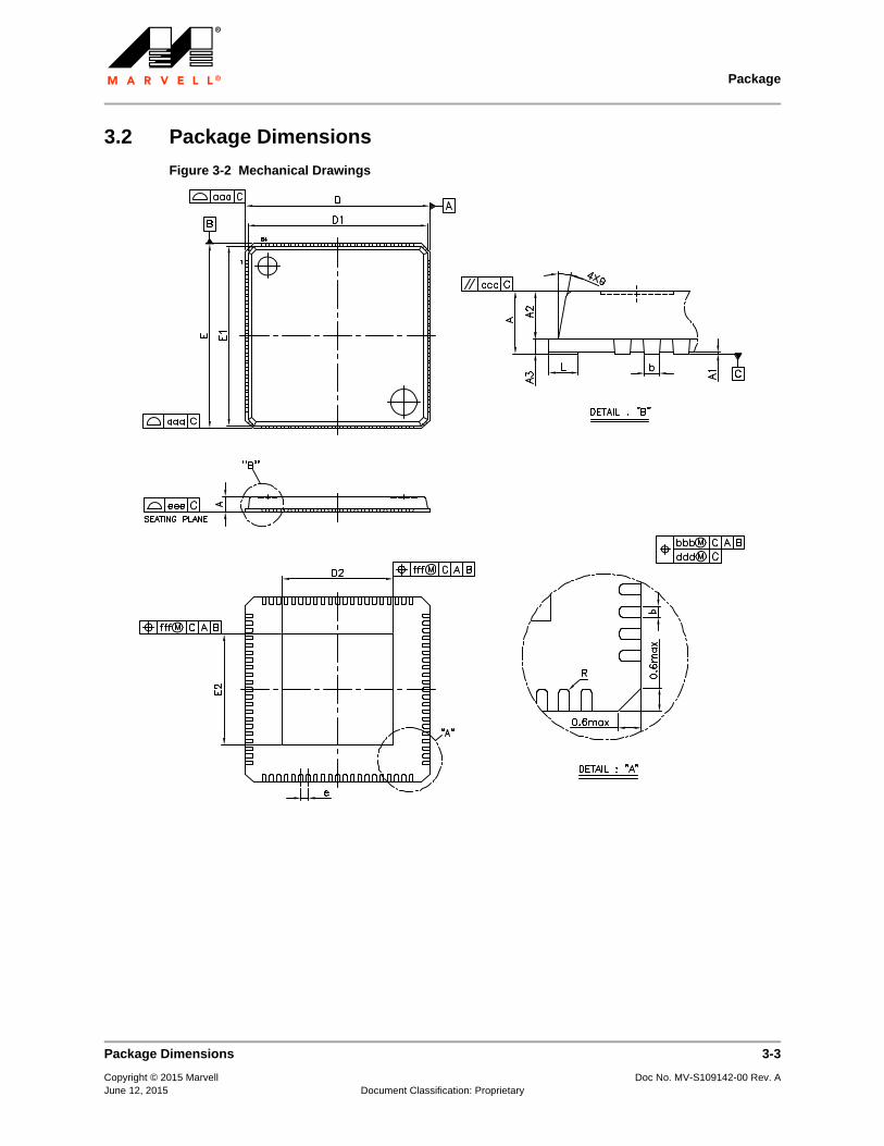
3.2 Package Dimensions
Figure 3-2 Mechanical Drawings
Package Dimensions 3-3
Copyright © 2015 Marvell Doc No. MV-S109142-00 Rev. AJune 12, 2015 Document Classification: Proprietary
88SM9705 SATA 6.0 Gbps: 1-to-5 Port MultiplierPreliminary Specifications
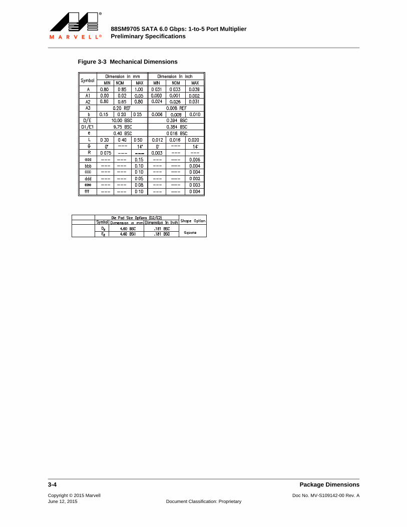
Figure 3-3 Mechanical Dimensions
3-4 Package Dimensions
Copyright © 2015 Marvell Doc No. MV-S109142-00 Rev. AJune 12, 2015 Document Classification: Proprietary

Package
3.3 Pin Descriptions
3.3.1 Pin Type Definitions
This section outlines the 88SM9705 pin descriptions. All signals ending with the letter N indicate an active-low signal. Pin type definitions are shown in the following table.
3.3.2 Pin List
Table 3-1 Pin Type Definitions
Pin Type Definition
I/O Input and output
I Input only
O Output only
PD Internal pull-down resistor (50 kΩ)
PU Internal pull-up resistor (50 kΩ)
mA DC sink capability
5 5V tolerance
Table 3-2 Serial ATA Interface Signals
Signal NameSignal Number
Type Description
P0_TXP 51 O Serial ATA Transmitter Differential Outputs.
P0_TXN 50 O
P1_TXP 17 O
P1_TXN 16 O
P2_TXP 11 O
P2_TXN 10 O
P3_TXP 5 O
P3_TXN 4 O
P4_TXP 63 O
P4_TXN 62 O
HT_TXP 53 O
HT_TXN 54 O
Pin Descriptions 3-5
Copyright © 2015 Marvell Doc No. MV-S109142-00 Rev. AJune 12, 2015 Document Classification: Proprietary
88SM9705 SATA 6.0 Gbps: 1-to-5 Port MultiplierPreliminary Specifications
P0_RXN 48 I Serial ATA Receiver Differential Inputs.
P0_RXP 47 I
P1_RXN 14 I
P1_RXP 13 I
P2_RXN 8 I
P2_RXP 7 I
P3_RXN 2 I
P3_RXP 1 I
P4_RXN 60 I
P4_RXP 59 I
HT_RXN 56 I
HT_RXP 57 I
Table 3-3 Chip Power-On Reset Signal
Signal NameSignal Number
Type Description
PWR_ON_RST_N 81 I Chip Power on Reset.
Active Low.
Table 3-4 UART Two-Wire Serial Interface
Signal NameSignal Number
Type Description
UAO 18 O UART Data Output.
UAI 19 I UART Data Input.
SCL 29 I/O Serial Clock
SDA 30 I/O Serial Data.
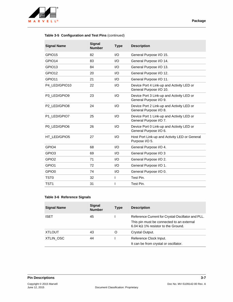
Table 3-5 Configuration and Test Pins
Signal NameSignal Number
Type Description
GPIO19 64 I/O General Purpose I/O 19.
GPIO18 65 I/O General Purpose I/O 18.
GPIO17 66 I/O General Purpose I/O 17.
GPIO16 67 I/O General Purpose I/O 16.
Table 3-2 Serial ATA Interface Signals (continued)
Signal NameSignal Number
Type Description
3-6 Pin Descriptions
Copyright © 2015 Marvell Doc No. MV-S109142-00 Rev. AJune 12, 2015 Document Classification: Proprietary
Package
GPIO15 82 I/O General Purpose I/O 15.
GPIO14 83 I/O General Purpose I/O 14.
GPIO13 84 I/O General Purpose I/O 13.
GPIO12 20 I/O General Purpose I/O 12.
GPIO11 21 I/O General Purpose I/O 11.
P4_LED/GPIO10 22 I/O Device Port 4 Link-up and Activity LED or General Purpose I/O 10.
P3_LED/GPIO9 23 I/O Device Port 3 Link-up and Activity LED or General Purpose I/O 9.
P2_LED/GPIO8 24 I/O Device Port 2 Link-up and Activity LED or General Purpose I/O 8.
P1_LED/GPIO7 25 I/O Device Port 1 Link-up and Activity LED or General Purpose I/O 7.
P0_LED/GPIO6 26 I/O Device Port 0 Link-up and Activity LED or General Purpose I/O 6.
HT_LED/GPIO5 27 I/O Host Port Link-up and Activity LED or General Purpose I/O 5.
GPIO4 68 I/O General Purpose I/O 4.
GPIO3 69 I/O General Purpose I/O 3
GPIO2 71 I/O General Purpose I/O 2.
GPIO1 72 I/O General Purpose I/O 1.
GPIO0 74 I/O General Purpose I/O 0.
TST0 32 I Test Pin.
TST1 31 I Test Pin.
Table 3-6 Reference Signals
Signal NameSignal Number
Type Description
ISET 45 I Reference Current for Crystal Oscillator and PLL.
This pin must be connected to an external 6.04 kΩ 1% resistor to the Ground.
XTLOUT 43 O Crystal Output.
XTLIN_OSC 44 I Reference Clock Input.
It can be from crystal or oscillator.
Table 3-5 Configuration and Test Pins (continued)
Signal NameSignal Number
Type Description
Pin Descriptions 3-7
Copyright © 2015 Marvell Doc No. MV-S109142-00 Rev. AJune 12, 2015 Document Classification: Proprietary

88SM9705 SATA 6.0 Gbps: 1-to-5 Port MultiplierPreliminary Specifications
Table 3-7 Power Pins
Signal Name
Signal Number Type Description
HT_VAA 55 I 1.8V Power Source for Host Port SATA PHY.
P0_VAA 49 I 1.8V Power Source for Device Port 0 SATA PHY.
P1_VAA 15 I 1.8V Power Source for Device Port 1 SATA PHY.
P2_VAA 9 I 1.8V Power Source for Device Port 2 SATA PHY.
P3_VAA 3 I 1.8V Power Source for Device Port 3 SATA PHY.
P4_VAA 61 I 1.8V Power Source for Device Port 4 SATA PHY.
VAA1 41 I 1.8V Power Source for Analog logic.
VSS1 42, 46 I Ground for Analog Logic.
P0_VSS 52 I Ground for SATA PHY.
P1_VSS 12 I Ground for SATA PHY.
P2_VSS 6 I Ground for SATA PHY.
HT_VSS 58 I Ground for SATA PHY.
VDDIO 33, 73 I 3.3 V Power Source for Digital IO.
VDD 28, 34, 70, 77 I 1.0 V Power Source for Digital.
Table 3-8 SPI Flash Interface Signals
Signal NameSignal Number
Type Description
SPI_DO 75 O Data Output of SPI Flash Interface.
SPI_CLK 79 O Clock Output of SPI Flash Interface.
SPI_CS 76 O Mode Select of SPI Flash Interface.
SPI_DI 78 I Data Input of SPI Flash Interface.
Table 3-9 Test Mode Interface Signals
Signal NameSignal Number
Type Description
TESTMODE 80 I Chip Test Mode.
TP 40 O Analog Test Point.
Table 3-10 Pins Not Connected
Signal NameSignal Number
Type Description
N/C 35, 36, 37, 38, 39
N/A Not Connected.
3-8 Pin Descriptions
Copyright © 2015 Marvell Doc No. MV-S109142-00 Rev. AJune 12, 2015 Document Classification: Proprietary
Layout Guidelines
4 LAYOUT GUIDELINES
This chapter describes the system recommendations from the Marvell Semiconductor design and application engineers who work with the 88SM9705. It is written for those who are designing schematics and printed circuit boards for an 88SM9705-based system. Whenever possible, the PCB designer must try to follow the suggestions provided in this chapter.
The information in this chapter is preliminary. Consult with Marvell Semiconductor design and application engineers before starting your PCB design.
The chapter contains the following sections:
Board Schematic Example
Layer Stack-Up
Power Supply
PCB Trace Routing
Recommended Layout
See Chapter 3, Package, for package information.
4-1
Copyright © 2015 Marvell Doc No. MV-S109142-00 Rev. AJune 12, 2015 Document Classification: Proprietary
88SM9705 SATA 6.0 Gbps: 1-to-5 Port MultiplierPreliminary Specifications
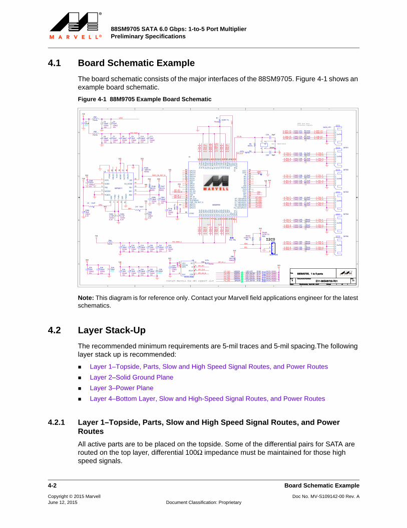
4.1 Board Schematic Example
The board schematic consists of the major interfaces of the 88SM9705. Figure 4-1 shows an example board schematic.
Figure 4-1 88M9705 Example Board Schematic
Note: This diagram is for reference only. Contact your Marvell field applications engineer for the latest schematics.
4.2 Layer Stack-Up
The recommended minimum requirements are 5-mil traces and 5-mil spacing.The following layer stack up is recommended:
Layer 1–Topside, Parts, Slow and High Speed Signal Routes, and Power Routes
Layer 2–Solid Ground Plane
Layer 3–Power Plane
Layer 4–Bottom Layer, Slow and High-Speed Signal Routes, and Power Routes
4.2.1 Layer 1–Topside, Parts, Slow and High Speed Signal Routes, and Power Routes
All active parts are to be placed on the topside. Some of the differential pairs for SATA are routed on the top layer, differential 100Ω impedance must be maintained for those high speed signals.
5
5
4
4
3
3
2
2
1
1
D D
C C
B B
A A
TXC - 7M25070024
I2C0
Contact Marvell for SPI support list
SATA host portInterface signals
S_TXP_HTS_TXN_HT
S_RXN_HTS_RXP_HT
S_RX0_PS_RX0_N
S_TX0_PS_TX0_N
S_TX1_PS_TX1_N
S_RX1_NS_RX1_P
S_TX2_PS_TX2_N
S_RX2_NS_RX2_P
S_TX3_PS_TX3_N
S_RX3_NS_RX3_P
S_TX4_PS_TX4_N
S_RX4_NS_RX4_P
S_T
XP
_HT
S_T
XN
_HT
S_R
XN
_HT
S_R
XP
_HT
S_R
X0_
PS
_RX
0_N
S_T
X0_
PS
_TX
0_N
S_T
X1_
PS
_TX
1_N
S_R
X1_
NS
_RX
1_P
S_T
X2_
PS
_TX
2_N
S_R
X2_
NS
_RX
2_P
S_T
X3_
PS
_TX
3_N
S_R
X3_
NS
_RX
3_P
S_T
X4_
PS
_TX
4_N
S_R
X4_
NS
_RX
4_P
XTLIN
ISE
T
VAA1
1V8_VAA2_1
XTLOUT
VAA1
1V8_VAA2_2
SCL
SDA
HT_LEDP0_LEDP1_LEDP2_LEDP3_LEDP4_LED
SPI_DO
SPI_DI_J
SPI_CLK
SPI_CS_N
SW2
SW1
PWR_ON_RST_N
SPI_DO
SPI_CLKSPI_DI_J
SPI_CS_NSCLSDA
HT_LEDP0_LEDP1_LEDP2_LEDP3_LEDP4_LED
C_RXP_HTC_RXN_HT
C_TXP_HTC_TXN_HT
C_RX0_PC_RX0_N
C_TX0_PC_TX0_N
C_TX1_PC_TX1_N
C_RX1_NC_RX1_P
C_TX2_PC_TX2_N
C_RX2_NC_RX2_P
C_TX3_PC_TX3_N
C_RX3_NC_RX3_P
C_TX4_PC_TX4_N
C_RX4_NC_RX4_P
1V8
3V31V0
1V0
3V3
3V3
1V8
1V0
3V3
3V3
3V3
3V3
3V3
3V3
3V3
3V3
1V8 3V3
3V3
1V0
1V0
Title
Size Document Number Rev
Date: Sheet of
EV1-88SM9705-R01 01
88SM9705, 1 to 5 ports
B
1 1Wednesday, April 08, 2015
Title
Size Document Number Rev
Date: Sheet of
EV1-88SM9705-R01 01
88SM9705, 1 to 5 ports
B
1 1Wednesday, April 08, 2015
Title
Size Document Number Rev
Date: Sheet of
EV1-88SM9705-R01 01
88SM9705, 1 to 5 ports
B
1 1Wednesday, April 08, 2015
C52 10nFC0402
C710nFC040216V
R513.01K-1%
R0402 R503.01K-1%R0402
C297100nFC040210V
R7
10K
-5%
R04
02
+ LED_HT1GREEN
C24 10nFC0402
R171 1K-5% R0402
TP1
C29510uFC06036.3V
C292100nFC040210V
R580-5%
R0402
C26 10nFC0402
C3310nFC040216V
C3522uF
C0805
C45 10nFC0402
C41 10nFC0402
R30-5%
C19100nFC040210V
KEY SATA4
S-ATA
1234567
C36 10nFC0402
R183 1K-5% R0402
R109100K-5%R0402
R10810K-5%R0402
I2C2
22-05-5035
11
22
33
+ LED_SATA2GREEN
C51 10nFC0402
C34100nFC040210V
C14 10nFC0402
C2944.7uFC04026.3V
FB1
Ferrite
U1
88SM9705
P3_
RX
P1
P3_
RX
N2
P3_
VA
A3
P3_
TX
N4
P3_
TX
P5
P2_
VS
S6
P2_
RX
P7
P2_
RX
N8
P2_
VA
A9
P2_
TX
N10
P2_
TX
P11
P1_
VS
S12
P1_
RX
P13
P1_
RX
N14
P1_
VA
A15
P1_
TX
N16
P1_
TX
P17
UA
O18
UA
I19
GP
IO12
20
GP
IO11
21X
TLO
UT
43X
TLI
N_O
SC
44IS
ET
45V
SS
146
P0_
RX
P47
P0_
RX
N48
P0_
VA
A49
P0_
TX
N50
P0_
TX
P51
P0_
VS
S52
HT
_TX
P53
HT
_TX
N54
HT
_VA
A55
HT
_RX
N56
HT
_RX
P57
HT
_VS
S58
P4_
RX
P59
P4_
RX
N60
P4_
VA
A61
P4_
TX
N62
P4_
TX
P63
P4_LED/GPIO1022P3_LED/GPIO923P2_LED/GPIO824P1_LED/GPIO725P0_LED/GPIO626HT_LED/GPIO527VDD28SCL29SDA30TST131TST032VDDIO33VDD34N/C35N/C36N/C37N/C38N/C39TP40VAA141VSS142
GPIO1964
GPIO1865
GPIO1766
GPIO1667
GPIO468
GPIO369
VDD70
GPIO271
GPIO172
VDDIO73
GPIO074
SPI_DO75
SPI_CS76
VDD77
SPI_DI78
SPI_CLK79
TESTMODE80
PWR_ON_RST_N81
GPIO1582
GPIO1483
GPIO1384
EPAD85
C16 16pF
C21100nFC040210V
C291100nFC040210V
C53 10nFC0402
+ LED_SATA0GREEN
C28100nFC040210V
C29610uFC06036.3V
R105 1K-5% R0402
C25 10nFC0402
C2934.7uFC04026.3V
R16.04K-1%
R0402
R170 1K-5% R0402
C47 10nFC0402
C17100nFC040210V
R51M-5%
C288100nFC040210V
U6
MX25L4006E
CS#1
SO2
WP#3
SI5
SCLK6
HOLD#7 VCC8
Gnd4
C122uF
C0805
C43 10nFC0402
C15 10nFC0402
C2100nFC040210V
C8100nFC040210V
C1110nFC040216V
C38 10nFC0402
C310nFC040216V
C50 10nFC0402
C2210nFC040216V
L9 1.0uH
R174 1K-5% R0402
C13 10nFC0402
KEYSATA_HT1
S-ATA
1234567
C6100nFC040210V
KEY SATA1
S-ATA
1234567
U3
88PG8211 FB113
SGND2
SVIN1 S
LEE
Pn
17S
W1
9
PGND25
PV
IN1
8
SW
26
PV
IN2
7
FB23
SS_DONE14
SDI15
EN211
PG
ND
110
MODE24
EN112
MO
DE
118
VLD
O19
VIN
LDO
20
PG
ND
21
EN
LDO
16
C46 10nFC0402
C2922uF
C0805C3110nFC040216V
KEY SATA2
S-ATA
1234567
C27 10nFC0402
+ LED_SATA1GREEN
TP3
KEY SATA3
S-ATA
1234567
FB2
Ferrite
R10710K-5%R0402
FB3
Ferrite
C48 10nFC0402
R169 1K-5% R0402
C40 10nFC0402
C1810nFC040216V
+ LED_SATA4GREEN
+ LED_SATA3GREEN
R8010K-5%R0402
C23 16pF
C910nFC040216V
KEY SATA5
S-ATA
1234567
C10100nFC040210V
Y2
25MHz
1 2
3 4
C42 10nFC0402
C39 10nFC0402
C2010nFC040216V
L10 1.0uH
C37 10nFC0402
C3010nFC040216V
C32100nFC040210V
TP2
C12 10nFC0402
C11610nFC040216V
4-2 Board Schematic Example
Copyright © 2015 Marvell Doc No. MV-S109142-00 Rev. AJune 12, 2015 Document Classification: Proprietary
Layout Guidelines
4.2.2 Layer 2–Solid Ground Plane
A solid ground plane must be located directly below the top layer of the PCB. This layer must be a minimum distance below the top layer to reduce the amount of crosstalk and EMI. No cutouts must exist in the ground plane. It is recommended to use 1 ounce copper.
4.2.3 Layer 3–Power Plane
Use solid planes on layer 3 to supply power to the ICs on the PCB. Avoid narrow traces and necks on this plane.
4.2.4 Layer 4–Bottom Layer, Slow and High-Speed Signal Routes, and Power Routes
Some of the differential pairs for SATA are routed on the top layer, differential 100Ω impedance must be maintained for those high speed signals. The high speed signals have the return current on the third layer, which is the power plane. No cut-out must exist under the signal path.
4.3 Power Supply
The 88SM9705 operates using the following power supplies:
VDD Power (1.0V)
Analog Power Supply (1.8V)
VDDIO Power (3.3V)
Power-on-Reset Timing Requirement
Bias Current Resistor (RSET)
4.3.1 VDD Power (1.0V)
All digital power pins (VDD pins) must be connected directly to a VDD plane in the power layer with short and wide traces to minimize digital power-trace inductances.
Use vias close to the VDD pins to connect to this plane and avoid using the traces on the top layer. Marvell recommends placing capacitors around the three sides of the PCB near VDD pins with the following dimensions:
1 nF (1 capacitor)
0.1 µF (2 capacitors)
2.2 µF (1 ceramic capacitor)
The 2.2 µF ceramic decoupling capacitor is needed to filter the lower frequency power-supply noise.
To reduce system noise, the use of high-frequency surface-mount monolithic ceramic bypass capacitors must be placed as close as possible to the channel VDD pins. At least one decoupling capacitor must be placed on each side of the IC package.
Power Supply 4-3
Copyright © 2015 Marvell Doc No. MV-S109142-00 Rev. AJune 12, 2015 Document Classification: Proprietary

88SM9705 SATA 6.0 Gbps: 1-to-5 Port MultiplierPreliminary Specifications
Short and wide copper traces must be used to minimize parasitic inductances. Low-value capacitors (1,000–10,000 pF) are preferable over higher values because they are more effective at higher frequencies.
4.3.2 Analog Power Supply (1.8V)
The 1.8V power is for analog design of the chip.
4.3.3 VDDIO Power (3.3V)
The digital power (3.3V) is the power supply for the digital pad.
4.3.4 Power-on-Reset Timing Requirement
The minimum timing requirement for power on reset is 50 µs after all power supplies are stable and before the power-on-reset signal is released.
4.3.5 Bias Current Resistor (RSET)
This resistor must connect a 6.04 KΩ (1%) resistor to the ISET pin and the adjacent top ground plane. It must lie as close as possible to the ISET pin.
4.4 PCB Trace Routing
The stack-up parameters for the reference board are shown in Table 4-1.
4.5 Recommended Layout
Solid ground planes are recommended. However, special care must be taken when routing VAA and VSS pins.
The following general tips describe what must be considered when determining your stack-up and board routing. These tips are not meant to substitute for consulting with a signal-integrity expert or doing your own simulations.
Note: Specific numbers or rules-of-thumb are not used here because they might not be applicable in every situation.
Table 4-1 PCB Board Stack-up Parameters
LayerLayer
DescriptionCopper Weight
(oz)Target Impedance
(±10%)
1 Signal 0.5 50
2 GND 1 N/A
3 Power 1 N/A
4 Signal 0.5 50
4-4 PCB Trace Routing
Copyright © 2015 Marvell Doc No. MV-S109142-00 Rev. AJune 12, 2015 Document Classification: Proprietary

Layout Guidelines
Do not split ground planes.
Keep good spacing between possible sensitive analog circuitry on your board and the digital signals to sufficiently isolate noise. A solid ground plane is necessary to provide a good return path for routing layers. Try to provide at least one ground plane adjacent to all routing layers (see Figure 4-2).
Keep trace layers as close as possible to the adjacent ground or power planes.
This helps minimize crosstalk and improve noise control on the planes.
Figure 4-2 Trace Has at Least One Solid Plane for Return Path
When routing adjacent to only a power plane, do not cross splits.
Route traces only over the power plane that supplies both the driver and the load. Otherwise, provide a decoupling capacitor near the trace at the end that is not supplied by the adjacent power plane.
Critical signals must avoid running parallel and close to or directly over a gap.
This would change the impedance of the trace.
Separate analog powers onto opposing planes.
This helps minimize the coupling area that an analog plane has with an adjacent digital plane.
For dual strip-line routing, traces must only cross at 90 degrees.
Avoid more than two routing layers in a row to minimize tandem crosstalk and to better control impedance.
Planes must be evenly distributed in order to minimize warping.
Calculating or modeling impedance must be made prior to routing.
This helps ensure that a reasonable trace thickness is used and that the desired board thickness is available. Consult with your board fabricator for accurate impedance.
Allow good separation between fast signals to avoid crosstalk.
Crosstalk increases as the parallel traces get longer.
GND
V2
V1
Recommended Layout 4-5
Copyright © 2015 Marvell Doc No. MV-S109142-00 Rev. AJune 12, 2015 Document Classification: Proprietary

88SM9705 SATA 6.0 Gbps: 1-to-5 Port MultiplierPreliminary Specifications
When packages become smaller, route traces over a split power plane
Smaller packages force vias to become smaller, thereby reducing board thickness and layer counts, which might create the need to route traces over a split power plane. Some alternatives to provide return path for these signals are listed below.
Caution must be used when applying these techniques. Digital traces must not cross over analog planes, and vice-versa. All of these rules must be followed closely to prevent noise contamination problems that might arise due to routing over the wrong plane.
By tightly controlling the return path, control noise on the power and ground planes can be controlled.
Place a ground layer close enough to the split power plane in order to couple enough to provide buried capacitance, such as SIG-PWR-GND (see Figure 4-3). Return signals that encounter splits in this situation simply jumps to the ground plane, over the split, and back to the other power plane. Buried capacitance provides the benefit of adding low inductance decoupling to your board. Your fabricator may charge for a special license fee and special materials. To determine the amount of capacitance your planes provide, use the following equation:
Where ER is the dielectric coefficient, L • W represents the area of copper, and H is the separation between planes.
Provide return-path capacitors that connect to both power planes and jumps the split. Place them close to the traces so that there is one capacitor for every four or five traces. The capacitors would then provide the return path (see Figure 4-4).
Allow only static or slow signals on layers where they are adjacent to split planes.
Figure 4-3 shows the ground layer close to the split power plane.
Figure 4-3 Close Power and Ground Planes Provide Coupling for Good Return Path
C 1.249 10 13–• Er• L• W H⁄•=
V2 PLANE
GND PLANE
V1 PLANEH
4-6 Recommended Layout
Copyright © 2015 Marvell Doc No. MV-S109142-00 Rev. AJune 12, 2015 Document Classification: Proprietary
Layout Guidelines
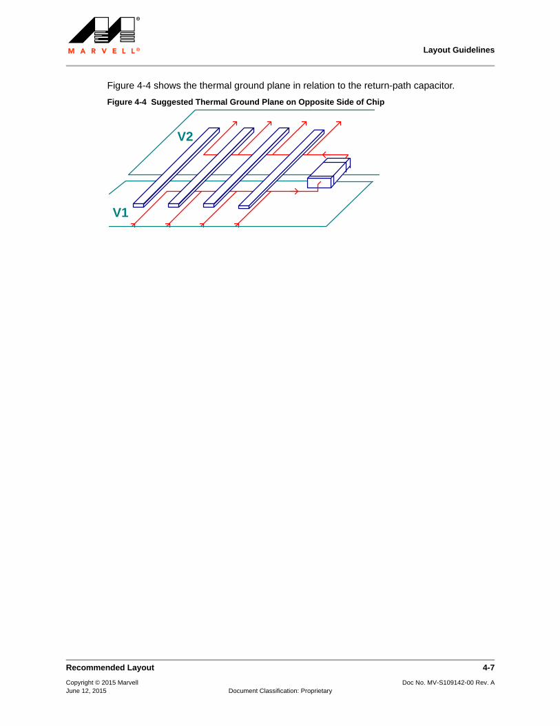
Figure 4-4 shows the thermal ground plane in relation to the return-path capacitor.
Figure 4-4 Suggested Thermal Ground Plane on Opposite Side of Chip
V1
V2
Recommended Layout 4-7
Copyright © 2015 Marvell Doc No. MV-S109142-00 Rev. AJune 12, 2015 Document Classification: Proprietary

88SM9705 SATA 6.0 Gbps: 1-to-5 Port MultiplierPreliminary Specifications
THIS PAGE LEFT INTENTIONALLY BLANK
4-8 Recommended Layout
Copyright © 2015 Marvell Doc No. MV-S109142-00 Rev. AJune 12, 2015 Document Classification: Proprietary
General Purpose I/O Port Interface
5 GENERAL PURPOSE I/O PORT INTERFACE
This chapter contains the following sections:
Overview
GPIO Normal Mode
GPIO Sample-at-Reset Pins
5-1
Copyright © 2015 Marvell Doc No. MV-S109142-00 Rev. AJune 12, 2015 Document Classification: Proprietary
88SM9705 SATA 6.0 Gbps: 1-to-5 Port MultiplierPreliminary Specifications
5.1 Overview
The 88SM9705 contains a 20-bit General Purpose Port Input/Output (GPIO) interface. The GPIO interface provides the following features:
Each of the GPIO pins can be assigned to act as a general purpose input or output pin.
A dedicated register provides the GPIO input value.
A dedicated register provides the GPIO output value.
Each of the GPIO outputs can be programmed for the LED to blink approximately every 100 ms.
5-2 Overview
Copyright © 2015 Marvell Doc No. MV-S109142-00 Rev. AJune 12, 2015 Document Classification: Proprietary

General Purpose I/O Port Interface
5.2 GPIO Normal Mode
Table 5-1 describes the function of the GPIO pins.
Table 5-1 GPIO Pin Default Functions
Pin NameDefault Setting
Default FunctionCapable Function
Source Description
GPIO0 PU General Purpose I/O LED blink for RAID
Selectable Multiple blink frequency
GPIO1 PU General Purpose I/O LED blink for RAID
Selectable Multiple blink frequency
GPIO2 PU General Purpose I/O LED blink for RAID
Selectable Multiple blink frequency
GPIO3 PU General Purpose I/O LED blink for RAID
Selectable Multiple blink frequency
GPIO4 PU Three-device-port mode: This function is Device 2 port link-up and activity LED
Otherwise: General Purpose I/O
0: LED blink for RAID
1: Notification SDB sending pulse output, pulse (1 µs)
2: System alert level output
Selectable Multiple blink frequency
GPIO5 PU Host port link-up and activity LED * LED blink for RAID
Selectable Multiple blink frequency
GPIO6 PU Device 0 port link-up and activity LED *
LED blink for RAID
Selectable Multiple blink frequency
GPIO7 PU Device 1 port link-up and activity LED *
LED blink for RAID
Selectable Multiple blink frequency
GPIO8 PU Device 2 port link-up and activity LED *
LED blink for RAID
Selectable Multiple blink frequency
GPIO9 PU Device 3 port link-up and activity LED *
LED blink for RAID
Selectable Multiple blink frequency
GPIO10 PU LED blink for RAID
Selectable Multiple blink frequency
GPIO11 PU General Purpose I/O LED blink for RAID
Selectable Multiple blink frequency
GPIO12 PU General Purpose I/O LED blink for RAID
Selectable Multiple blink frequency
GPIO13 PU General Purpose I/O LED blink for RAID
Selectable Multiple blink frequency
GPIO14 PU General Purpose I/O LED blink for RAID
Selectable Multiple blink frequency
GPIO15 PU General Purpose I/O General Purpose I/O
N/A
GPIO Normal Mode 5-3
Copyright © 2015 Marvell Doc No. MV-S109142-00 Rev. AJune 12, 2015 Document Classification: Proprietary

88SM9705 SATA 6.0 Gbps: 1-to-5 Port MultiplierPreliminary Specifications
GPIO16 PU System alert level output General Purpose I/O
N/A Send level when system alert condition is met
GPIO17 PU General Purpose I/O General Purpose I/O
N/A N/A
GPIO18 PU General Purpose I/O Power management: POW_OIT
N/A N/A
GPIO19 PU General Purpose I/O Power management: POW_IN
N/A N/A
* The link up and activity can be separated and selectable for the blink source.
Table 5-1 GPIO Pin Default Functions (continued)
Pin NameDefault Setting
Default FunctionCapable Function
Source Description
5-4 GPIO Normal Mode
Copyright © 2015 Marvell Doc No. MV-S109142-00 Rev. AJune 12, 2015 Document Classification: Proprietary
General Purpose I/O Port Interface
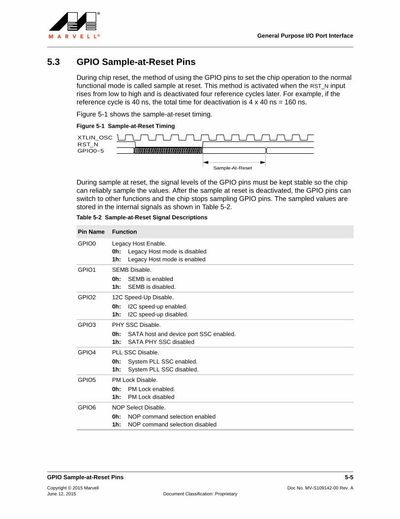
5.3 GPIO Sample-at-Reset Pins
During chip reset, the method of using the GPIO pins to set the chip operation to the normal functional mode is called sample at reset. This method is activated when the RST_N input rises from low to high and is deactivated four reference cycles later. For example, if the reference cycle is 40 ns, the total time for deactivation is 4 x 40 ns = 160 ns.
Figure 5-1 shows the sample-at-reset timing.
Figure 5-1 Sample-at-Reset Timing
During sample at reset, the signal levels of the GPIO pins must be kept stable so the chip can reliably sample the values. After the sample at reset is deactivated, the GPIO pins can switch to other functions and the chip stops sampling GPIO pins. The sampled values are stored in the internal signals as shown in Table 5-2.
Table 5-2 Sample-at-Reset Signal Descriptions
Pin Name Function
GPIO0 Legacy Host Enable.0h: Legacy Host mode is disabled1h: Legacy Host mode is enabled
GPIO1 SEMB Disable.
0h: SEMB is enabled1h: SEMB is disabled.
GPIO2 12C Speed-Up Disable.
0h: I2C speed-up enabled.1h: I2C speed-up disabled.
GPIO3 PHY SSC Disable.
0h: SATA host and device port SSC enabled.1h: SATA PHY SSC disabled
GPIO4 PLL SSC Disable.
0h: System PLL SSC enabled.1h: System PLL SSC disabled.
GPIO5 PM Lock Disable.
0h: PM Lock enabled.1h: PM Lock disabled
GPIO6 NOP Select Disable.
0h: NOP command selection enabled1h: NOP command selection disabled
Sample-At-Reset
XTLIN_OSCRST_NGPIO0~5
GPIO Sample-at-Reset Pins 5-5
Copyright © 2015 Marvell Doc No. MV-S109142-00 Rev. AJune 12, 2015 Document Classification: Proprietary
88SM9705 SATA 6.0 Gbps: 1-to-5 Port MultiplierPreliminary Specifications
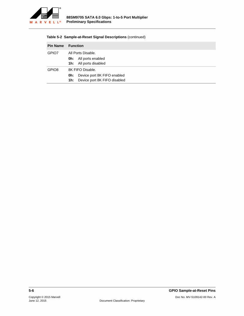
GPIO7 All Ports Disable.
0h: All ports enabled1h: All ports disabled
GPIO8 8K FIFO Disable.
0h: Device port 8K FIFO enabled1h: Device port 8K FIFO disabled
Table 5-2 Sample-at-Reset Signal Descriptions (continued)
Pin Name Function
5-6 GPIO Sample-at-Reset Pins
Copyright © 2015 Marvell Doc No. MV-S109142-00 Rev. AJune 12, 2015 Document Classification: Proprietary
UART Interface
6 UART INTERFACE
This chapter contains the following sections:
UART Interface Overview
UART Interface Timing
Register Access Sequence Through UART
6-1
Copyright © 2015 Marvell Doc No. MV-S109142-00 Rev. AJune 12, 2015 Document Classification: Proprietary
88SM9705 SATA 6.0 Gbps: 1-to-5 Port MultiplierPreliminary Specifications
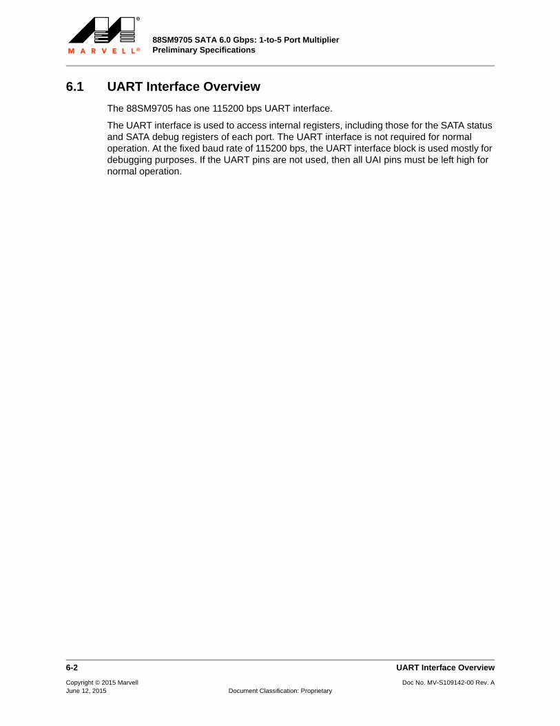
6.1 UART Interface Overview
The 88SM9705 has one 115200 bps UART interface.
The UART interface is used to access internal registers, including those for the SATA status and SATA debug registers of each port. The UART interface is not required for normal operation. At the fixed baud rate of 115200 bps, the UART interface block is used mostly for debugging purposes. If the UART pins are not used, then all UAI pins must be left high for normal operation.
6-2 UART Interface Overview
Copyright © 2015 Marvell Doc No. MV-S109142-00 Rev. AJune 12, 2015 Document Classification: Proprietary

UART Interface
6.2 UART Interface Timing
Figure 6-1 illustrates an example of UART signal timing.
Figure 6-1 UART Signal Timing Example
D0 D1 D2 D3 D4 D5 D6 D7
1 Character
UART Interface Timing 6-3
Copyright © 2015 Marvell Doc No. MV-S109142-00 Rev. AJune 12, 2015 Document Classification: Proprietary
88SM9705 SATA 6.0 Gbps: 1-to-5 Port MultiplierPreliminary Specifications
6.3 Register Access Sequence Through UART
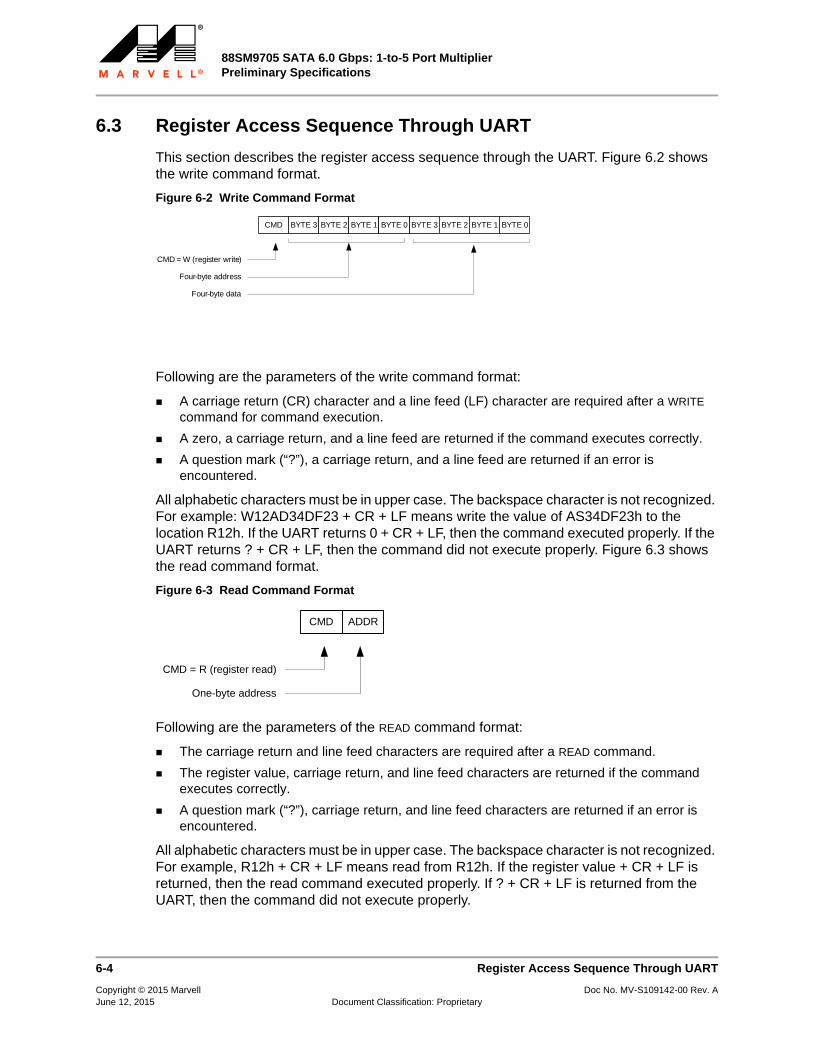
This section describes the register access sequence through the UART. Figure 6.2 shows the write command format.
Figure 6-2 Write Command Format
Following are the parameters of the write command format:
A carriage return (CR) character and a line feed (LF) character are required after a WRITE command for command execution.
A zero, a carriage return, and a line feed are returned if the command executes correctly.
A question mark (“?”), a carriage return, and a line feed are returned if an error is encountered.
All alphabetic characters must be in upper case. The backspace character is not recognized. For example: W12AD34DF23 + CR + LF means write the value of AS34DF23h to the location R12h. If the UART returns 0 + CR + LF, then the command executed properly. If the UART returns ? + CR + LF, then the command did not execute properly. Figure 6.3 shows the read command format.
Figure 6-3 Read Command Format
Following are the parameters of the READ command format:
The carriage return and line feed characters are required after a READ command.
The register value, carriage return, and line feed characters are returned if the command executes correctly.
A question mark (“?”), carriage return, and line feed characters are returned if an error is encountered.
All alphabetic characters must be in upper case. The backspace character is not recognized. For example, R12h + CR + LF means read from R12h. If the register value + CR + LF is returned, then the read command executed properly. If ? + CR + LF is returned from the UART, then the command did not execute properly.
CMD
CMD = W (register write)
Four-byte address
Four-byte data
BYTE 3 BYTE 2 BYTE 1 BYTE 0BYTE 3 BYTE 2 BYTE 1 BYTE 0
CMD ADDR
CMD = R (register read)
One-byte address
6-4 Register Access Sequence Through UART
Copyright © 2015 Marvell Doc No. MV-S109142-00 Rev. AJune 12, 2015 Document Classification: Proprietary
UART Interface
6.3.1 UART Read/Write Command Sequences
Each UART sequence includes the parity bit in the last bit. Table 6-1 through Table 6-4, Write Command, Error detail the register Read/Write sequences for Read and Write commands, with and without errors.
Table 6-1 describes the registers read command sequence when no errors are returned.
Table 6-2 describes the registers read command sequence when errors are returned.
Table 6-1 Read Command, No Error
Byte Master Slave Value
1 CMD(R) - 52h
2
3
ADDR[31:24] - ASCII (ADDR[31:28])
ASCII (ADDR[27:24])
4
5
ADDR[23:16] - ASCII (ADDR[23:20])
ASCII (ADDR[19:16])
6
7
ADDR[15:8] - ASCII (ADDR[15:12])
ASCII (ADDR[11:8])
8
9
ADDR[7:0] - ASCII (ADDR[7:4])
ASCII (ADDR[3:0])
10 CR - 0Dh
11 LF - 0Ah
12
13
- DATA[31:24] ASCII (DATA[31:28])
ASCII (DATA[27:24])
14
15
- DATA[23:16] ASCII (DATA[23:20])
ASCII (DATA[19:16])
16
17
- DATA[15:8] ASCII (DATA[15:12])
ASCII (DATA[11:8])
18
19
- DATA[7:0] ASCII (DATA[7:4])
ASCII (DATA[3:0])
20 - CR 0Dh
21 - LF 0Ah
Table 6-2 Read Command, Error
Byte Master Slave Value
1 CMD(R) - 52h
2
3
ADDR[31:24] - ASCII (ADDR[31:28])
ASCII (ADDR[27:24])
4
5
ADDR[23:16] - ASCII (ADDR[23:20])
ASCII (ADDR[19:16])
6
7
ADDR[15:8] - ASCII (ADDR[15:12])
ASCII (ADDR[11:8])
Register Access Sequence Through UART 6-5
Copyright © 2015 Marvell Doc No. MV-S109142-00 Rev. AJune 12, 2015 Document Classification: Proprietary
88SM9705 SATA 6.0 Gbps: 1-to-5 Port MultiplierPreliminary Specifications
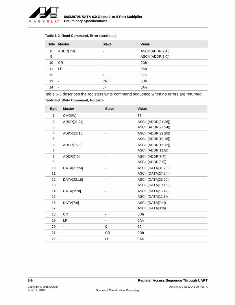
Table 6-3 describes the registers write command sequence when no errors are returned.
8
9
ADDR[7:0] - ASCII (ADDR[7:4])
ASCII (ADDR[3:0])
10 CR - 0Dh
11 LF - 0Ah
12 ? 3Fh
13 - CR 0Dh
14 - LF 0Ah
Table 6-3 Write Command, No Error
Byte Master Slave Value
1 CMD(W) - 57h
2
3
ADDR[31:24] - ASCII (ADDR[31:28])
ASCII (ADDR[27:24])
4
5
ADDR[23:16] - ASCII (ADDR[23:20])
ASCII (ADDR[19:16])
6
7
ADDR[15:8] - ASCII (ADDR[15:12])
ASCII (ADDR[11:8])
8
9
ADDR[7:0] - ASCII (ADDR[7:4])
ASCII (ADDR[3:0])
10
11
DATA[31:24] - ASCII (DATA[31:28])
ASCII (DATA[27:24])
12
13
DATA[23:16] - ASCII (DATA[23:20])
ASCII (DATA[19:16])
14
15
DATA[15:8] - ASCII (DATA[15:12])
ASCII (DATA[11:8])
16
17
DATA[7:0] - ASCII (DATA[7:4])
ASCII (DATA[3:0])
18 CR - 0Dh
19 LF - 0Ah
20 - 0 30h
21 - CR 0Dh
22 - LF 0Ah
Table 6-2 Read Command, Error (continued)
Byte Master Slave Value
6-6 Register Access Sequence Through UART
Copyright © 2015 Marvell Doc No. MV-S109142-00 Rev. AJune 12, 2015 Document Classification: Proprietary
UART Interface
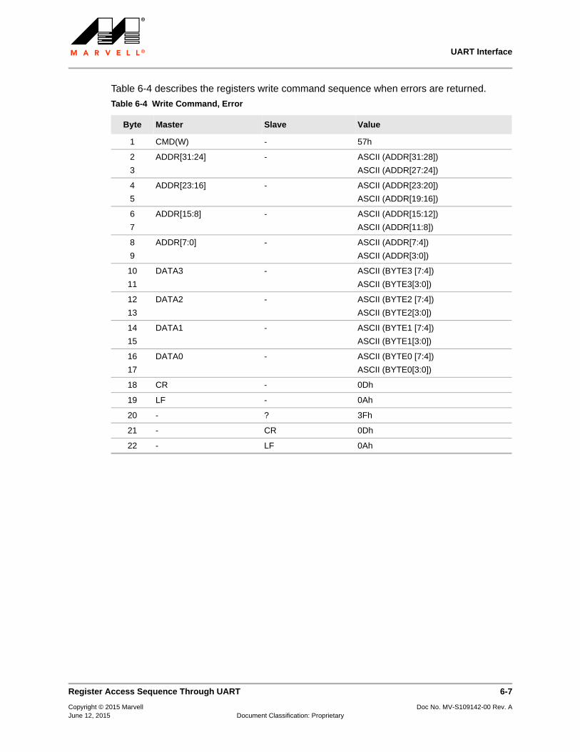
Table 6-4 describes the registers write command sequence when errors are returned.
Table 6-4 Write Command, Error
Byte Master Slave Value
1 CMD(W) - 57h
2
3
ADDR[31:24] - ASCII (ADDR[31:28])
ASCII (ADDR[27:24])
4
5
ADDR[23:16] - ASCII (ADDR[23:20])
ASCII (ADDR[19:16])
6
7
ADDR[15:8] - ASCII (ADDR[15:12])
ASCII (ADDR[11:8])
8
9
ADDR[7:0] - ASCII (ADDR[7:4])
ASCII (ADDR[3:0])
10
11
DATA3 - ASCII (BYTE3 [7:4])
ASCII (BYTE3[3:0])
12
13
DATA2 - ASCII (BYTE2 [7:4])
ASCII (BYTE2[3:0])
14
15
DATA1 - ASCII (BYTE1 [7:4])
ASCII (BYTE1[3:0])
16
17
DATA0 - ASCII (BYTE0 [7:4])
ASCII (BYTE0[3:0])
18 CR - 0Dh
19 LF - 0Ah
20 - ? 3Fh
21 - CR 0Dh
22 - LF 0Ah
Register Access Sequence Through UART 6-7
Copyright © 2015 Marvell Doc No. MV-S109142-00 Rev. AJune 12, 2015 Document Classification: Proprietary
88SM9705 SATA 6.0 Gbps: 1-to-5 Port MultiplierPreliminary Specifications
THIS PAGE LEFT INTENTIONALLY BLANK
6-8 Register Access Sequence Through UART
Copyright © 2015 Marvell Doc No. MV-S109142-00 Rev. AJune 12, 2015 Document Classification: Proprietary
Ports
7 PORTS
This chapter contains the following sections:
PM_PORT Field
Control Ports
Cascading
7-1
Copyright © 2015 Marvell Doc No. MV-S109142-00 Rev. AJune 12, 2015 Document Classification: Proprietary
88SM9705 SATA 6.0 Gbps: 1-to-5 Port MultiplierPreliminary Specifications
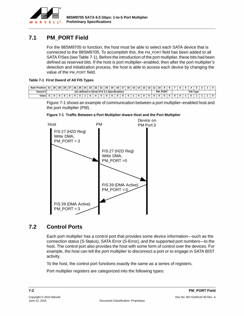
7.1 PM_PORT Field
For the 88SM9705 to function, the host must be able to select each SATA device that is connected to the 88SM9705. To accomplish this, the PM_PORT field has been added to all SATA FISes (see Table 7-1). Before the introduction of the port multiplier, these bits had been defined as reserved bits. If the host is port multiplier–enabled, then after the port multiplier’s detection and initialization process, the host is able to access each device by changing the value of the PM_PORT field.
Table 7-1 First Dword of All FIS Types
Figure 7-1 shows an example of communication between a port multiplier–enabled host and the port multiplier (PM).
Figure 7-1 Traffic Between a Port Multiplier-Aware Host and the Port Multiplier
7.2 Control Ports
Each port multiplier has a control port that provides some device information—such as the connection status (S-Status), SATA Error (S-Error), and the supported port numbers—to the host. The control port also provides the host with some form of control over the devices. For example, the host can tell the port multiplier to disconnect a port or to engage in SATA BIST activity.
To the host, the control port functions exactly the same as a series of registers.
Port multiplier registers are categorized into the following types:
Byte Position 31 30 29 28 27 26 25 24 23 22 21 20 19 18 17 16 15 14 13 12 11 10 9 8 7 6 5 4 3 2 1 0
Dword 0 (As defined in Serial ATA 3.1 Specification) PM_PORT FIS Type
Value 0 0 0 0 0 0 0 1 0 0 0 0 0 0 0 0 1 0 0 0 0 0 0 0 0 0 1 0 1 1 1 0
Host PM
FIS 39 (DMA Active)PM_PORT = 3
FIS 27 (H2D Reg)Write DMA, PM_PORT = 3
Device on PM Port 3
FIS 27 (H2D Reg)Write DMA, PM_PORT =0
FIS 39 (DMA Active)PM_PORT = 0
7-2 PM_PORT Field
Copyright © 2015 Marvell Doc No. MV-S109142-00 Rev. AJune 12, 2015 Document Classification: Proprietary
Ports
General Status and Control Registers (GSCR)
Port Status and Control Registers (PSCR).
Each port multiplier has only one set of GSCR and one set of PSCR for each port.
For more information on the GSCR and PSCR registers, see Chapter 8, Registers.
The host can access the port multiplier’s control port as port Fh by using the READ BUFFER (E4h) and WRITE BUFFER (E8h) ATA commands. See section 8.1.1, Register Access from Host and UART for more detail on how these ATA commands can be used with the port multiplier.
7.3 Cascading
The port multiplier should not be cascaded. Do not connect a port multiplier to another port multiplier.
Cascading 7-3
Copyright © 2015 Marvell Doc No. MV-S109142-00 Rev. AJune 12, 2015 Document Classification: Proprietary

88SM9705 SATA 6.0 Gbps: 1-to-5 Port MultiplierPreliminary Specifications
THIS PAGE LEFT INTENTIONALLY BLANK
7-4 Cascading
Copyright © 2015 Marvell Doc No. MV-S109142-00 Rev. AJune 12, 2015 Document Classification: Proprietary
Registers
8 REGISTERS
This chapter contains the following sections:
Register Summary
Register Map Summary
Register Description
8-1
Copyright © 2015 Marvell Doc No. MV-S109142-00 Rev. AJune 12, 2015 Document Classification: Proprietary
88SM9705 SATA 6.0 Gbps: 1-to-5 Port MultiplierPreliminary Specifications
8.1 Register Summary
This section contains the following subsections:
Register Access from Host and UART
General Status and Control Registers
Vendor-Specific Port Multiplier Control Registers
Host Port PHY Event Counter Registers
General Purpose Input/Output (GPIO) Registers
SATA PHY and Link Registers
Device Port PHY Event Counter Registers
8.1.1 Register Access from Host and UART
Registers can be accessed from either the host (SATA) or the UART.
8.1.1.1 Accessing from the Host
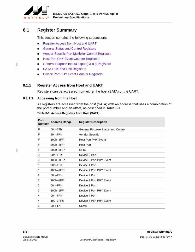
All registers are accessed from the host (SATA) with an address that uses a combination of the port number and an offset, as described in Table 8-1
Table 8-1 Access Registers from Host (SATA)
Port Number
Address Range Register Description
F 00h–7Fh General Purpose Status and Control
F 80h–FFh Vendor Specific
F 100h–1FFh Host Port PHY Event
F 200h–2FFh Host Port
F 300h–3FFh GPIO
0 00h–FFh Device 0 Port
0 100h–1FFh Device 0 Port PHY Event
1 00h–FFh Device 1 Port
1 100h–1FFh Device 1 Port PHY Event
2 00h–FFh Device 2 Port
2 100h–1FFh Device 2 Port PHY Event
3 00h–FFh Device 3 Port
3 100h–1FFh Device 3 Port PHY Event
4 00h–FFh Device 4 Port
4 100–1FFh Device 4 Port PHY Event
5 00–FFh SEMB
8-2 Register Summary
Copyright © 2015 Marvell Doc No. MV-S109142-00 Rev. AJune 12, 2015 Document Classification: Proprietary
Registers
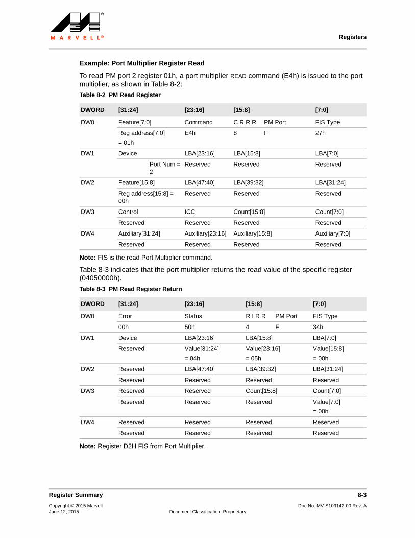
Example: Port Multiplier Register Read
To read PM port 2 register 01h, a port multiplier READ command (E4h) is issued to the port multiplier, as shown in Table 8-2:
Note: FIS is the read Port Multiplier command.
Table 8-3 indicates that the port multiplier returns the read value of the specific register (04050000h).
Note: Register D2H FIS from Port Multiplier.
Table 8-2 PM Read Register
DWORD [31:24] [23:16] [15:8] [7:0]
DW0 Feature[7:0] Command C R R R PM Port FIS Type
Reg address[7:0]
= 01h
E4h 8 F 27h
DW1 Device LBA[23:16] LBA[15:8] LBA[7:0]
Port Num = 2
Reserved Reserved Reserved
DW2 Feature[15:8] LBA[47:40] LBA[39:32] LBA[31:24]
Reg address[15:8] = 00h
Reserved Reserved Reserved
DW3 Control ICC Count[15:8] Count[7:0]
Reserved Reserved Reserved Reserved
DW4 Auxiliary[31:24] Auxiliary[23:16] Auxiliary[15:8] Auxiliary[7:0]
Reserved Reserved Reserved Reserved
Table 8-3 PM Read Register Return
DWORD [31:24] [23:16] [15:8] [7:0]
DW0 Error Status R I R R PM Port FIS Type
00h 50h 4 F 34h
DW1 Device LBA[23:16] LBA[15:8] LBA[7:0]
Reserved Value[31:24]
= 04h
Value[23:16]
= 05h
Value[15:8]
= 00h
DW2 Reserved LBA[47:40] LBA[39:32] LBA[31:24]
Reserved Reserved Reserved Reserved
DW3 Reserved Reserved Count[15:8] Count[7:0]
Reserved Reserved Reserved Value[7:0]
= 00h
DW4 Reserved Reserved Reserved Reserved
Reserved Reserved Reserved Reserved
Register Summary 8-3
Copyright © 2015 Marvell Doc No. MV-S109142-00 Rev. AJune 12, 2015 Document Classification: Proprietary

88SM9705 SATA 6.0 Gbps: 1-to-5 Port MultiplierPreliminary Specifications
Example: Port Multiplier Register Write
To write to PM port F register 90h with a value of CAFE1F1Fh, a PM WRITE command (E8h) is issued to the PM as shown in Table 8-4.
Note: FIS is the write Port Multiplier command.
8.1.1.2 Accessing from UART
All registers are accessed from UART with a base address of R00020xxxh.
The following items show read and write examples of accessing a General Purpose register with offset 58h:
Read—R00020058h
Write—W00020058A5A5A5A5 (write A5A5A5A5 to register 58h).
Table 8-5 shows the address offset ranges and descriptions for register access from UART.
Table 8-4 PM Write Register
DWORD [31:24] [23:16] [15:8] [7:0]
DW0 Feature[7:0] Command C R R R PM Port FIS Type
Reg address[7:0]
= 90h
E8h 8 F 27h
DW1 Device LBA[23:16] LBA[15:8] LBA[7:0]
Port = F Value[31:24]
= CAh
Value[23:16]
= FEh
Value[15:8]
= 1Fh
DW2 Feature[15:8] LBA[47:40] LBA[39:32] LBA[31:24]
Reg address[15:8] = 00h
Reserved Reserved Reserved
DW3 Control ICC Count[15:8] Count[7:0]
Reserved Reserved Reserved Value[7:0] = 1Fh
DW4 Auxiliary[31:24] Auxiliary[23:16] Auxiliary[15:8] Auxiliary[7:0]
Reserved Reserved Reserved Reserved
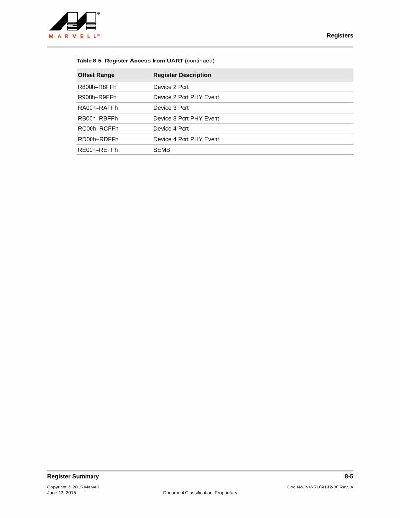
Table 8-5 Register Access from UART
Offset Range Register Description
R000h–R07Fh General Status and Control
R080h–R0FFh Vendor-Specific
R1A0h–R1FFh GPIO
R200h–R2FFh Host Port
R300h–R3FFh Host Port PHY Event
R400h–R4FFh Device 0 Port
R500h–R5FFh Device 0 Port PHY Event
R600h–R6FFh Device 1 Port
R700h–R7FFh Device 1 Port PHY Event
8-4 Register Summary
Copyright © 2015 Marvell Doc No. MV-S109142-00 Rev. AJune 12, 2015 Document Classification: Proprietary
Registers
R800h–R8FFh Device 2 Port
R900h–R9FFh Device 2 Port PHY Event
RA00h–RAFFh Device 3 Port
RB00h–RBFFh Device 3 Port PHY Event
RC00h–RCFFh Device 4 Port
RD00h–RDFFh Device 4 Port PHY Event
RE00h–REFFh SEMB
Table 8-5 Register Access from UART (continued)
Offset Range Register Description
Register Summary 8-5
Copyright © 2015 Marvell Doc No. MV-S109142-00 Rev. AJune 12, 2015 Document Classification: Proprietary

88SM9705 SATA 6.0 Gbps: 1-to-5 Port MultiplierPreliminary Specifications
8.1.2 General Status and Control Registers
8.1.3 Vendor-Specific Port Multiplier Control Registers
8.1.4 Host Port PHY Event Counter Registers
Table 8-6 General Purpose Status and Control Register Summary
Register Default Value Register Description Location
R000h VVVV1B4Bh Product Identifier Page 8-12
R001h 0000A00Eh Revision Information Page 8-12
R002h 0000000Vh Port Information Page 8-13
R020h 00000000h Error Information Page 8-13
R021h 0400FFFFh Error Information Bit Enable Page 8-13
R022h 00000000h PHY Event Counter Control Page 8-14
R040h 0000001Fh Port Multiplier Revision 1 X Features Support Page 8-15
R060h 00000001h Port Multiplier 1 X Feature Enable Page 8-15
Table 8-7 Vendor-Specific PM Control Register Summary
Register Default Value Register Description Location
R080h 00000000h PM Control Page 8-17
R081h 00000000h Probe Control Page 8-18
R082h 00000000h Probe Signal Page 8-18
R083h 0000003Eh PM Lock Control Page 8-19
R084h 00000000h PM Lock Status Page 8-19
R086h 00002C2Bh SEMB I2C Control Page 8-20
R087h 00900000h SEMB Time-out Value Page 8-20
R089h 00000000h PLL Control 1 Page 8-21
R08Ah 8000003Fh PLL Control 2 Page 8-21
R091h F81E003Ah FIFO Size Control Page 8-22
R092h 00000666h Memory Control Page 8-23
R093h 00888888h SATA Port PHY Control Page 8-23
R0A0h 00000000h Side Bank Address Register Page 8-24
R0A1h 00000000h Side Bank Data Register Page 8-24
Table 8-8 Host Port PHY Event Counter Register Summary
Register Default Value Register Description Location
R100h 00000000h Host Port PHY Event Counter 1 Page 8-25
8-6 Register Summary
Copyright © 2015 Marvell Doc No. MV-S109142-00 Rev. AJune 12, 2015 Document Classification: Proprietary

Registers
8.1.5 General Purpose Input/Output (GPIO) Registers
8.1.6 SATA PHY and Link Registers
This section includes the following sections:
Link Registers
SATA PHY—Low-Power SERDES PHY Registers
Table 8-9 GPIO Register Summary
Register Default Value Register Description Location
R3A0h 00000000h GPIO Data Out Page 8-25
R3A4h 000107C0h GPIO Data Out Enable Page 8-25
R3A8h 00000000h GPIO Blink Enable Page 8-26
R3ACh 00000000h GPIO Data In Polarity Page 8-26
R3B0h 00000000h GPIO Data In Page 8-26
R3C4h 2AF624C3h GPIO [6] through GPIO [11] Port Source Select Page 8-27
R3C8h 047868C0h Power-Control Logic Time-Out Control Register Page 8-32
R3D8h 255AD6B5h GPIO [0] through GPIO [5] Port Source Select Page 8-33
R3E0h 2A2AD6B5h GPIO[12] through GPIO[17] Port Source Select Page 8-39
R3E4h 000002B5h GPIO[18] through GPIO[19] Port Source Select Page 8-42
R3E8h 00000041h Blink Rate Counter Register for SATA4 and Overall Link Page 8-42
R3ECh 01041041h Blink Rate Counter Register for SATA0/1/2/3/H Page 8-43
R3F0h 01041041h Blink Rate Counter Register for GPIO_OUT[4] through GPIO_OUT[0]
Page 8-44
R3F4h 01041041h Blink Rate Counter Register for GPIO_OUT[9] through GPIO_OUT[5]
Page 8-45
R3F8h 01041041h Blink Rate Counter Register for GPIO_OUT[14] through GPIO_OUT[10]
Page 8-46
R3FCh 01041041h Blink Rate Counter Register for GPIO_OUT[19] through GPIO_OUT[15]
Page 8-46
Register Summary 8-7
Copyright © 2015 Marvell Doc No. MV-S109142-00 Rev. AJune 12, 2015 Document Classification: Proprietary
88SM9705 SATA 6.0 Gbps: 1-to-5 Port MultiplierPreliminary Specifications
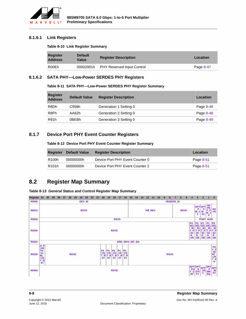
8.1.6.1 Link Registers
8.1.6.2 SATA PHY—Low-Power SERDES PHY Registers
8.1.7 Device Port PHY Event Counter Registers
8.2 Register Map Summary
Table 8-10 Link Register Summary
Register Address
Default Value
Register Description Location
R00Eh 00002001h PHY Reserved Input Control Page 8-47
Table 8-11 SATA PHY—Low-Power SERDES PHY Register Summary
Register Address
Default Value Register Description Location
R8Dh C958h Generation 1 Setting 0 Page 8-48
R8Fh AA62h Generation 2 Setting 0 Page 8-48
R91h 0BEBh Generation 3 Setting 0 Page 8-49
Table 8-12 Device Port PHY Event Counter Register Summary
Register Default Value Register Description Location
R100h 00000000h Device Port PHY Event Counter 0 Page 8-51
R101h 00000000h Device Port PHY Event Counter 2 Page 8-51
Table 8-13 General Status and Control Register Map Summary
Register 31 30 29 28 27 26 25 24 23 22 21 20 19 18 17 16 15 14 13 12 11 10 9 8 7 6 5 4 3 2 1 0
R000h DEV_ID VENDOR_ID
R001h RSVD PM_REV RSVD
SPT_P
M_12
SPT_PM_S1
SPPRT_PM_1
0
RSVD
R002h RSVD PORT_NUM
R020h RSVD
P4_SEL_BIT_PSCR_OR
P3_SEL_BIT_PSCR_OR
P2_SEL_BIT_PSCR_OR
P1_SEL_BIT_PSCR_OR
P0_SEL_BIT_PSCR_OR
R021h ERR_INFO_BIT_EN
R022h
H_PORTH_GLBL_CNT_RST
RSVD
P4_CNT_RST
P3_CNT_RST
P2_CNT_RST
P1_CNT_RST
P0_CNT_RST
RSVD
PHY_EVE
NT_CNT_E
N
R040h RSVD
SPT_PHY_CNT
SPT_NOTIFY
SPT_SS
C
SPT_PMREQ
SPT_BIST
8-8 Register Map Summary
Copyright © 2015 Marvell Doc No. MV-S109142-00 Rev. AJune 12, 2015 Document Classification: Proprietary

Registers
R060h RSVD
NOTIFY_E
N
SSC_E
N
PMREQP_EN
BIST_E
N
Table 8-14 Vendor-Specific Port Multiplier Control Register Map Summary
Register 31 30 29 28 27 26 25 24 23 22 21 20 19 18 17 16 15 14 13 12 11 10 9 8 7 6 5 4 3 2 1 0
R080h RSVD
SEMB_MEMBIST_TEST_FAIL
SEMB_MEMBIST_TEST_FIN
PORT_4_MEMBIST_TEST_FAIL
PORT_4_MEMBIST_TEST_FIN
PORT_3_MEMBIST_TEST_FAIL
PORT_3_MEMBIST_TEST_FIN
PORT_2_MEMBIST_TEST_FAIL
PORT_2_MEMBIST_TEST_FIN
PORT_1_MEMBIST_TEST_FAIL
PORT_1_MEMBIST_TEST_FIN
PORT_0_MEMBIST_TEST_FAIL
PORT_0_MEMBIST_TEST_FIN
PM_CTL_MEMBIST_TEST_FAIL
PM_CTL_MEMBIST_TEST_FIN
RSVD
NOP_COM_EN
ALL_DEV_E
N
HOST_DEV_INV
I2C_SPEE
D_SEL
R081h RSVD PROBE_MON_SEL
PROBE_MOD_SEL PROBE_SIG_SEL
R082h RSVD PROBE_SIG
R083h
LOCK_NOTIFY_EN
RSVD
SET_DEV_BIT_FISREL_LOCK_E
N
D2H_FIS_REL_LOCK_E
N
SET_DEV_BIT_FIS_LOCK_EN
DMA_SET
UP_FISLOCK_EN
H2D_FIS_LOCK_EN
PM_LOCK_EN
R084h RSVD
PM_LOCK_VALID
PM_LOCK_PORT_ID
R086h RSVD
SEMB_INTR
SEMB_WR
SEMB_ADDR SEMB_RD_WR_DATA RSVD SEP_TWOWIRE_SERIAL_ADD RS
VD SEMB_TWOWIRE_SERIAL_ADD
R087h RSVD SEMB_TO_VAL
R089h RSVD
ANA_GROUP_TESTSEL
ANA_GROUP_
GAINX2
ANA_GROUP_BYPASS
ANA_GROUP_BG
_SELPLL_TEST_MON
PLL_SCC_RE
SET_EX
T
PLL_SCC_FREQ_DIV
PLL_SSC_GAINX2
PLL_SSC_MODE
PLL_PU_SS
C
PLL_SSC_E
N
R08Ah PU_PLL
RSVD PLL_SSC_RNG RSVD RS
VDRSVD
SYSCLK_EN
SATA_DEV_4_CLK_E
N
SATA_DEV_3_CLK_E
N
SATA_DEV_2_CLK_E
N
SATA_DEV_1_CLK_E
N
SATA_DEV_0_CLK_E
N
R091h FIFO_SIZE_THRESH_SEL FIFO_SIZE_THRESH RSVD PM_CTL_FIFO_FLOW_CTL_THRSH
R092h RSVDSEMB_1P_MEM_
WTC
SEMB_1P_MEM_
RTC
PORT_2P_MEM_
WTC
PORT_2P_MEM_
RTC
PM_CTL_2P_MEM_WTC
PM_CTL_2P_MEM_RTC
R093h RSVDPORT4_PU
PORT4_SPD_SEL
PORT3_PU
PORT3_SPEED_SEL
PORT2_PU
PORT2_SPEED_SEL
PORT1_PU
PORT1_SPEED_SEL
PORT0_PU
PORT0_SPEED_SEL
HOST_PORT_PU
HOST_PORT_SPEED_SEL
R0A0h
SPI_MEM_ACCESS
RSVD UNIT_SEL MEM_ADD
R0A1h SIDE_BANK_ACCESS
Table 8-15 Host Port PHY Event Counter Register Map Summary
Register 31 30 29 28 27 26 25 24 23 22 21 20 19 18 17 16 15 14 13 12 11 10 9 8 7 6 5 4 3 2 1 0
R100h PHY_EVENT_CNT_1
Table 8-13 General Status and Control Register Map Summary (continued)
Register 31 30 29 28 27 26 25 24 23 22 21 20 19 18 17 16 15 14 13 12 11 10 9 8 7 6 5 4 3 2 1 0
Register Map Summary 8-9
Copyright © 2015 Marvell Doc No. MV-S109142-00 Rev. AJune 12, 2015 Document Classification: Proprietary
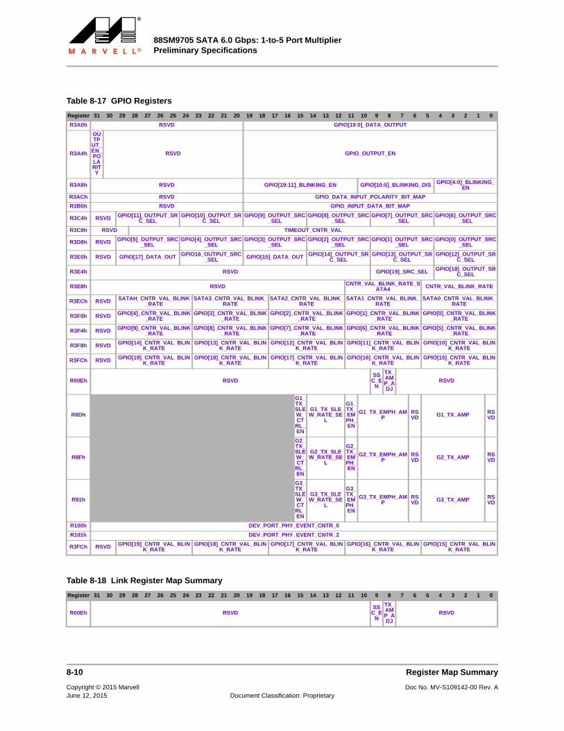
88SM9705 SATA 6.0 Gbps: 1-to-5 Port MultiplierPreliminary Specifications
Table 8-17 GPIO Registers
Register 31 30 29 28 27 26 25 24 23 22 21 20 19 18 17 16 15 14 13 12 11 10 9 8 7 6 5 4 3 2 1 0
R3A0h RSVD GPIO[19:0]_DATA_OUTPUT
R3A4h
OUTP
UT_EN_POLARITY
RSVD GPIO_OUTPUT_EN
R3A8h RSVD GPIO[19:11]_BLINKING_EN GPIO[10:5]_BLINKING_DIS GPIO[4:0]_BLINKING_EN
R3ACh RSVD GPIO_DATA_INPUT_POLARITY_BIT_MAP
R3B0h RSVD GPIO_INPUT_DATA_BIT_MAP
R3C4h RSVD GPIO[11]_OUTPUT_SRC_SEL
GPIO[10]_OUTPUT_SRC_SEL
GPIO[9]_OUTPUT_SRC_SEL
GPIO[8]_OUTPUT_SRC_SEL
GPIO[7]_OUTPUT_SRC_SEL
GPIO[6]_OUTPUT_SRC_SEL
R3C8h RSVD TIMEOUT_CNTR_VAL
R3D8h RSVD GPIO[5]_OUTPUT_SRC_SEL
GPIO[4]_OUTPUT_SRC_SEL
GPIO[3]_OUTPUT_SRC_SEL
GPIO[2]_OUTPUT_SRC_SEL
GPIO[1]_OUTPUT_SRC_SEL
GPIO[0]_OUTPUT_SRC_SEL
R3E0h RSVD GPIO[17]_DATA_OUT GPIO16_OUTPUT_SRC_SEL GPIO[15]_DATA_OUT GPIO[14]_OUTPUT_SR
C_SELGPIO[13]_OUTPUT_SR
C_SELGPIO[12]_OUTPUT_SR
C_SEL
R3E4h RSVD GPIO[19]_SRC_SEL GPIO[18]_OUTPUT_SRC_SEL
R3E8h RSVD CNTR_VAL_BLINK_RATE_SATA4 CNTR_VAL_BLINK_RATE
R3ECh RSVD SATAH_CNTR_VAL_BLINK_RATE
SATA3_CNTR_VAL_BLINK_RATE
SATA2_CNTR_VAL_BLINK_RATE
SATA1_CNTR_VAL_BLINK_RATE
SATA0_CNTR_VAL_BLINK_RATE
R3F0h RSVD GPIO[4]_CNTR_VAL_BLINK_RATE
GPIO[3]_CNTR_VAL_BLINK_RATE
GPIO[2]_CNTR_VAL_BLINK_RATE
GPIO[1]_CNTR_VAL_BLINK_RATE
GPIO[0]_CNTR_VAL_BLINK_RATE
R3F4h RSVD GPIO[9]_CNTR_VAL_BLINK_RATE
GPIO[8]_CNTR_VAL_BLINK_RATE
GPIO[7]_CNTR_VAL_BLINK_RATE
GPIO[6]_CNTR_VAL_BLINK_RATE
GPIO[5]_CNTR_VAL_BLINK_RATE
R3F8h RSVD GPIO[14]_CNTR_VAL_BLINK_RATE
GPIO[13]_CNTR_VAL_BLINK_RATE
GPIO[12]_CNTR_VAL_BLINK_RATE
GPIO[11]_CNTR_VAL_BLINK_RATE
GPIO[10]_CNTR_VAL_BLINK_RATE
R3FCh RSVD GPIO[19]_CNTR_VAL_BLINK_RATE
GPIO[18]_CNTR_VAL_BLINK_RATE
GPIO[17]_CNTR_VAL_BLINK_RATE
GPIO[16]_CNTR_VAL_BLINK_RATE
GPIO[15]_CNTR_VAL_BLINK_RATE
R00Eh RSVDSS
C_EN
TX_AMP_ADJ
RSVD
R8Dh
G1_TX_SLEW_CT
RL_EN
G1_TX_SLEW_RATE_SE
L
G1_TX_EMPH_EN
G1_TX_EMPH_AMP
RSVD G1_TX_AMP RS
VD
R8Fh
G2_TX_SLEW_CT
RL_EN
G2_TX_SLEW_RATE_SE
L
G2_TX_EMPH_EN
G2_TX_EMPH_AMP
RSVD G2_TX_AMP RS
VD
R91h
G3_TX_SLEW_CT
RL_EN
G3_TX_SLEW_RATE_SE
L
G3_TX_EMPH_EN
G3_TX_EMPH_AMP
RSVD G3_TX_AMP RS
VD
R100h DEV_PORT_PHY_EVENT_CNTR_0
R101h DEV_PORT_PHY_EVENT_CNTR_2
R3FCh RSVD GPIO[19]_CNTR_VAL_BLINK_RATE
GPIO[18]_CNTR_VAL_BLINK_RATE
GPIO[17]_CNTR_VAL_BLINK_RATE
GPIO[16]_CNTR_VAL_BLINK_RATE
GPIO[15]_CNTR_VAL_BLINK_RATE
Table 8-18 Link Register Map Summary
Register 31 30 29 28 27 26 25 24 23 22 21 20 19 18 17 16 15 14 13 12 11 10 9 8 7 6 5 4 3 2 1 0
R00Eh RSVDSS
C_EN
TX_AMP_ADJ
RSVD
8-10 Register Map Summary
Copyright © 2015 Marvell Doc No. MV-S109142-00 Rev. AJune 12, 2015 Document Classification: Proprietary
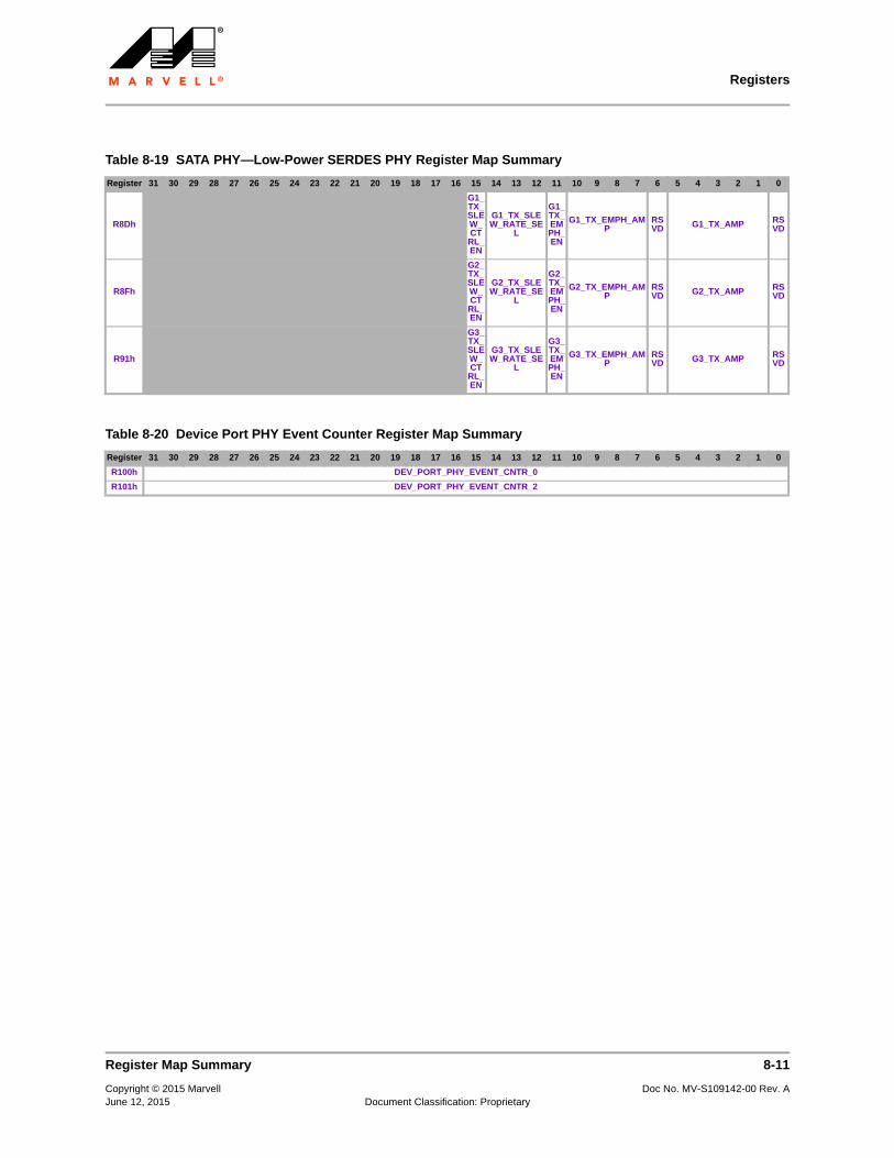
Registers
Table 8-19 SATA PHY—Low-Power SERDES PHY Register Map Summary
Register 31 30 29 28 27 26 25 24 23 22 21 20 19 18 17 16 15 14 13 12 11 10 9 8 7 6 5 4 3 2 1 0
R8Dh
G1_TX_SLEW_CT
RL_EN
G1_TX_SLEW_RATE_SE
L
G1_TX_EMPH_EN
G1_TX_EMPH_AMP
RSVD G1_TX_AMP RS
VD
R8Fh
G2_TX_SLEW_CT
RL_EN
G2_TX_SLEW_RATE_SE
L
G2_TX_EMPH_EN
G2_TX_EMPH_AMP
RSVD G2_TX_AMP RS
VD
R91h
G3_TX_SLEW_CT
RL_EN
G3_TX_SLEW_RATE_SE
L
G3_TX_EMPH_EN
G3_TX_EMPH_AMP
RSVD G3_TX_AMP RS
VD
Table 8-20 Device Port PHY Event Counter Register Map Summary
Register 31 30 29 28 27 26 25 24 23 22 21 20 19 18 17 16 15 14 13 12 11 10 9 8 7 6 5 4 3 2 1 0
R100h DEV_PORT_PHY_EVENT_CNTR_0
R101h DEV_PORT_PHY_EVENT_CNTR_2
Register Map Summary 8-11
Copyright © 2015 Marvell Doc No. MV-S109142-00 Rev. AJune 12, 2015 Document Classification: Proprietary

88SM9705 SATA 6.0 Gbps: 1-to-5 Port MultiplierPreliminary Specifications
8.3 Register Description
This section contains the following subsections:
General Status and Control Registers
Vendor-Specific Port Multiplier Control Registers
Host Port PHY Event Counter Registers
SATA PHY and Link Registers
Device Port PHY Event Counter Registers
8.3.1 General Status and Control Registers
R000h (VVVV1B4Bh) • Product IdentifierBit Position 31 30 29 28 27 26 25 24 23 22 21 20 19 18 17 16 15 14 13 12 11 10 9 8 7 6 5 4 3 2 1 0
Bits DEV_ID VENDOR_ID
Default Value V V V V V V V V V V V V V V V V 0 0 0 1 1 0 1 1 0 1 0 0 1 0 1 1
Bits Field NameRead/Write
Default Value
Description
31:16 DEV_ID R VVVVh Product Identifier.
9705h: 1-to-5 Port Multiplier
15:0 VENDOR_ID R 1B4Bh Vendor Identifier.
R001h (0000A00Eh) • Revision InformationBit Position 31 30 29 28 27 26 25 24 23 22 21 20 19 18 17 16 15 14 13 12 11 10 9 8 7 6 5 4 3 2 1 0
Bits RSVD PM_REV RSVD
SPT_P
M_12
SPT_P
M_S1
SPPRT_P
M_10
RSVD
Default Value 0 0 0 0 0 0 0 0 0 0 0 0 0 0 0 0 1 0 1 0 0 0 0 0 0 0 0 0 1 1 1 0
Bits Field NameRead/Write
Default Value
Description
31:16 RSVD R 0000h Reserved.
Do not change the default value.
15:8 PM_REV R A0h Port Multiplier Revision.
7:4 RSVD R 0h Reserved.
3 SPT_PM_12 R 1h Support for Port Multiplier Specification 1.2.
2 SPT_PM_S1 R 1h Support for Port Multiplier Specification 1.1.
1 SPPRT_PM_10 R 1h Support for Port Multiplier Specification 1.0.
0 RSVD R 0h Reserved.
Do not change the default value.
8-12 Register Description
Copyright © 2015 Marvell Doc No. MV-S109142-00 Rev. AJune 12, 2015 Document Classification: Proprietary
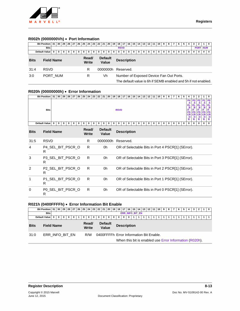
Registers
R002h (0000000Vh) • Port InformationBit Position 31 30 29 28 27 26 25 24 23 22 21 20 19 18 17 16 15 14 13 12 11 10 9 8 7 6 5 4 3 2 1 0
Bits RSVD PORT_NUM
Default Value 0 0 0 0 0 0 0 0 0 0 0 0 0 0 0 0 0 0 0 0 0 0 0 0 0 0 0 0 V V V V
Bits Field NameRead/Write
Default Value
Description
31:4 RSVD R 0000000h Reserved.
3:0 PORT_NUM R Vh Number of Exposed Device Fan Out Ports.
The default value is 6h if SEMB enabled and 5h if not enabled.
R020h (00000000h) • Error InformationBit Position 31 30 29 28 27 26 25 24 23 22 21 20 19 18 17 16 15 14 13 12 11 10 9 8 7 6 5 4 3 2 1 0
Bits RSVD
P4_SEL_BIT_PSCR_OR
P3_SEL_BIT_PSCR_OR
P2_SEL_BIT_PSCR_OR
P1_SEL_BIT_PSCR_OR
P0_SEL_BIT_PSCR_OR
Default Value 0 0 0 0 0 0 0 0 0 0 0 0 0 0 0 0 0 0 0 0 0 0 0 0 0 0 0 0 0 0 0 0
Bits Field NameRead/Write
Default Value
Description
31:5 RSVD R 0000000h Reserved.
4 P4_SEL_BIT_PSCR_OR
R 0h OR of Selectable Bits in Port 4 PSCR[1] (SError).
3 P3_SEL_BIT_PSCR_OR
R 0h OR of Selectable Bits in Port 3 PSCR[1] (SError).
2 P2_SEL_BIT_PSCR_OR
R 0h OR of Selectable Bits in Port 2 PSCR[1] (SError).
1 P1_SEL_BIT_PSCR_OR
R 0h OR of Selectable Bits in Port 1 PSCR[1] (SError).
0 P0_SEL_BIT_PSCR_OR
R 0h OR of Selectable Bits in Port 0 PSCR[1] (SError).
R021h (0400FFFFh) • Error Information Bit Enable Bit Position 31 30 29 28 27 26 25 24 23 22 21 20 19 18 17 16 15 14 13 12 11 10 9 8 7 6 5 4 3 2 1 0
Bits ERR_INFO_BIT_EN
Default Value 0 0 0 0 0 1 0 0 0 0 0 0 0 0 0 0 1 1 1 1 1 1 1 1 1 1 1 1 1 1 1 1
Bits Field NameRead/Write
Default Value
Description
31:0 ERR_INFO_BIT_EN R/W 0400FFFFh Error Information Bit Enable.
When this bit is enabled use Error Information (R020h).
Register Description 8-13
Copyright © 2015 Marvell Doc No. MV-S109142-00 Rev. AJune 12, 2015 Document Classification: Proprietary
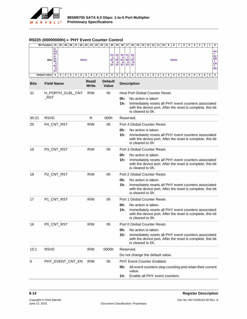
88SM9705 SATA 6.0 Gbps: 1-to-5 Port MultiplierPreliminary Specifications
R022h (00000000h) • PHY Event Counter Control Bit Position 31 30 29 28 27 26 25 24 23 22 21 20 19 18 17 16 15 14 13 12 11 10 9 8 7 6 5 4 3 2 1 0
Bits
H_PORTH_GLBL_CNT_RST
RSVD
P4_CNT_RST
P3_CNT_RST
P2_CNT_RST
P1_CNT_RST
P0_CNT_RST
RSVD
PHY_EVENT_CNT_EN
Default Value 0 0 0 0 0 0 0 0 0 0 0 0 0 0 0 0 0 0 0 0 0 0 0 0 0 0 0 0 0 0 0 0
Bits Field NameRead/Write
Default Value
Description
31 H_PORTH_GLBL_CNT_RST
R/W 0h Host Port Global Counter Reset.
0h: No action is taken1h: Immediately resets all PHY event counters associated
with the device port. After the reset is complete, this bit is cleared to 0h.
30:21 RSVD R 000h Reserved.
20 P4_CNT_RST R/W 0h Port 4 Global Counter Reset.
0h: No action is taken.1h: Immediately resets all PHY event counters associated
with the device port. After the reset is complete, this bit is cleared to 0h.
19 P3_CNT_RST R/W 0h Port 3 Global Counter Reset.
0h: No action is taken.1h: Immediately resets all PHY event counters associated
with the device port. After the reset is complete, this bit is cleared to 0h.
18 P2_CNT_RST R/W 0h Port 2 Global Counter Reset.
0h: No action is taken.1h: Immediately resets all PHY event counters associated
with the device port. After the reset is complete, this bit is cleared to 0h.
17 P1_CNT_RST R/W 0h Port 1 Global Counter Reset.
0h: No action is taken.1h: Immediately resets all PHY event counters associated
with the device port. After the reset is complete, this bit is cleared to 0h.
16 P0_CNT_RST R/W 0h Port 0 Global Counter Reset.
0h: No action is taken.1h: Immediately resets all PHY event counters associated
with the device port. After the reset is complete, this bit is cleared to 0h.
15:1 RSVD R/W 0000h Reserved.
Do not change the default value.
0 PHY_EVENT_CNT_EN R/W 0h PHY Event Counter Enabled.
0h: All event counters stop counting and retain their current value.
1h: Enable all PHY event counters.
8-14 Register Description
Copyright © 2015 Marvell Doc No. MV-S109142-00 Rev. AJune 12, 2015 Document Classification: Proprietary

Registers
R040h (0000001Fh) • Port Multiplier Revision 1 X Features SupportBit Position 31 30 29 28 27 26 25 24 23 22 21 20 19 18 17 16 15 14 13 12 11 10 9 8 7 6 5 4 3 2 1 0
Bits RSVD
SPT_PHY_CNT
SPT_N
OTIFY
SPT_SSC
SPT_PM
REQ
SPT_BIST
Default Value 0 0 0 0 0 0 0 0 0 0 0 0 0 0 0 0 0 0 0 0 0 0 0 0 0 0 0 1 1 1 1 1
Bits Field NameRead/Write
Default Value
Description
31:5 RSVD R 0000000h Reserved.
Do not change the default value.
4 SPT_PHY_CNT R 1h Support PHY Event Counter.
0h: Does not support PHY event counters.1h: Supports PHY event counters.
3 SPT_NOTIFY R 1h Support Asynchronous Notification.
This bit toggles asynchronous set bit device (SDB) notification.
0h: Does not support SDB notification.1h: Supports SDB notification.
2 SPT_SSC R 1h Support Dynamic SSC Transmit Enable.
This bit toggles support for dynamic spread spectrum clock (SSC) transmission.
0h: Does not support SSC transmit.1h: Supports SSC transmit.
1 SPT_PMREQ R 1h Support PMREQp.
0h: Does not support issuing a PMREQp to the host.1h: Supports issuing a PMREQp to the host.
0 SPT_BIST R 1h Support BIST.
0h: Does not support BIST.1h: Supports BIST.
R060h (00000001h) • Port Multiplier 1 X Feature EnableBit Position 31 30 29 28 27 26 25 24 23 22 21 20 19 18 17 16 15 14 13 12 11 10 9 8 7 6 5 4 3 2 1 0
Bits RSVD
NOTIFY_EN
SSC_EN
PM
REQP_EN
BIST_EN
Default Value 0 0 0 0 0 0 0 0 0 0 0 0 0 0 0 0 0 0 0 0 0 0 0 0 0 0 0 0 0 0 0 1
Bits Field NameRead/Write
Default Value
Description
31:4 RSVD R 0000000h Reserved.
Do not change the default value.
Register Description 8-15
Copyright © 2015 Marvell Doc No. MV-S109142-00 Rev. AJune 12, 2015 Document Classification: Proprietary
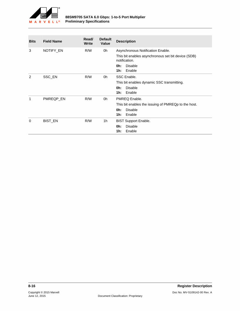
88SM9705 SATA 6.0 Gbps: 1-to-5 Port MultiplierPreliminary Specifications
3 NOTIFY_EN R/W 0h Asynchronous Notification Enable.
This bit enables asynchronous set bit device (SDB) notification.
0h: Disable1h: Enable
2 SSC_EN R/W 0h SSC Enable.
This bit enables dynamic SSC transmitting.
0h: Disable1h: Enable
1 PMREQP_EN R/W 0h PMREQ Enable.
This bit enables the issuing of PMREQp to the host.
0h: Disable1h: Enable
0 BIST_EN R/W 1h BIST Support Enable.
0h: Disable1h: Enable
Bits Field NameRead/Write
Default Value
Description
8-16 Register Description
Copyright © 2015 Marvell Doc No. MV-S109142-00 Rev. AJune 12, 2015 Document Classification: Proprietary
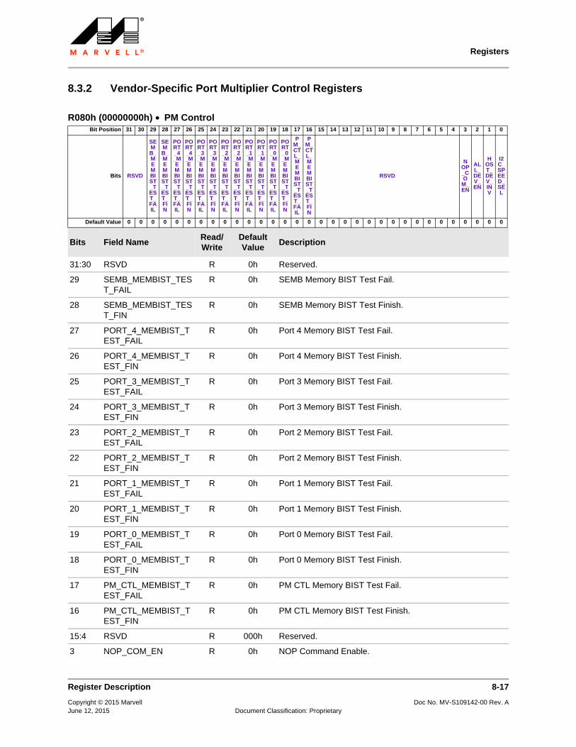
Registers
8.3.2 Vendor-Specific Port Multiplier Control Registers
R080h (00000000h) • PM ControlBit Position 31 30 29 28 27 26 25 24 23 22 21 20 19 18 17 16 15 14 13 12 11 10 9 8 7 6 5 4 3 2 1 0
Bits RSVD
SEMB_MEMBIST_TEST_FAIL
SEMB_MEMBIST_TEST_FIN
PORT_4_MEMBIST_TEST_FAIL
PORT_4_MEMBIST_TEST_FIN
PORT_3_MEMBIST_TEST_FAIL
PORT_3_MEMBIST_TEST_FIN
PORT_2_MEMBIST_TEST_FAIL
PORT_2_MEMBIST_TEST_FIN
PORT_1_MEMBIST_TEST_FAIL
PORT_1_MEMBIST_TEST_FIN
PORT_0_MEMBIST_TEST_FAIL
PORT_0_MEMBIST_TEST_FIN
PM_CTL_MEMBIST_TEST_FAIL
PM_CTL_MEMBIST_TEST_FIN
RSVD
NOP_CO
M_EN
ALL_DEV_EN
HOST_DEV_INV
I2C_SPEED_SEL
Default Value 0 0 0 0 0 0 0 0 0 0 0 0 0 0 0 0 0 0 0 0 0 0 0 0 0 0 0 0 0 0 0 0
Bits Field NameRead/Write
Default Value
Description
31:30 RSVD R 0h Reserved.
29 SEMB_MEMBIST_TEST_FAIL
R 0h SEMB Memory BIST Test Fail.
28 SEMB_MEMBIST_TEST_FIN
R 0h SEMB Memory BIST Test Finish.
27 PORT_4_MEMBIST_TEST_FAIL
R 0h Port 4 Memory BIST Test Fail.
26 PORT_4_MEMBIST_TEST_FIN
R 0h Port 4 Memory BIST Test Finish.
25 PORT_3_MEMBIST_TEST_FAIL
R 0h Port 3 Memory BIST Test Fail.
24 PORT_3_MEMBIST_TEST_FIN
R 0h Port 3 Memory BIST Test Finish.
23 PORT_2_MEMBIST_TEST_FAIL
R 0h Port 2 Memory BIST Test Fail.
22 PORT_2_MEMBIST_TEST_FIN
R 0h Port 2 Memory BIST Test Finish.
21 PORT_1_MEMBIST_TEST_FAIL
R 0h Port 1 Memory BIST Test Fail.
20 PORT_1_MEMBIST_TEST_FIN
R 0h Port 1 Memory BIST Test Finish.
19 PORT_0_MEMBIST_TEST_FAIL
R 0h Port 0 Memory BIST Test Fail.
18 PORT_0_MEMBIST_TEST_FIN
R 0h Port 0 Memory BIST Test Finish.
17 PM_CTL_MEMBIST_TEST_FAIL
R 0h PM CTL Memory BIST Test Fail.
16 PM_CTL_MEMBIST_TEST_FIN
R 0h PM CTL Memory BIST Test Finish.
15:4 RSVD R 000h Reserved.
3 NOP_COM_EN R 0h NOP Command Enable.
Register Description 8-17
Copyright © 2015 Marvell Doc No. MV-S109142-00 Rev. AJune 12, 2015 Document Classification: Proprietary

88SM9705 SATA 6.0 Gbps: 1-to-5 Port MultiplierPreliminary Specifications
2 ALL_DEV_EN R 0h All Devices Enable.
1 HOST_DEV_INV R 0h Host Device Inversion.
0 I2C_SPEED_SEL R 0h I2C Speed Select.
R081h (00000000h) • Probe ControlBit Position 31 30 29 28 27 26 25 24 23 22 21 20 19 18 17 16 15 14 13 12 11 10 9 8 7 6 5 4 3 2 1 0
Bits RSVD PROBE_MON_SEL
PROBE_MOD_SEL
PROBE_SIG_SEL
Default Value 0 0 0 0 0 0 0 0 0 0 0 0 0 0 0 0 0 0 0 0 0 0 0 0 0 0 0 0 0 0 0 0
Bits Field NameRead/Write
Default Value
Description
31:12 RSVD R 00000h Reserved.
11:8 PROBE_MON_SEL R/W 0h Probe Monitor Select.
7:4 PROBE_MOD_SEL R/W 0h Probe Module Select.
3:0 PROBE_SIG_SEL R/W 0h Probe Signal Select.
R082h (00000000h) • Probe SignalBit Position 31 30 29 28 27 26 25 24 23 22 21 20 19 18 17 16 15 14 13 12 11 10 9 8 7 6 5 4 3 2 1 0
Bits RSVD PROBE_SIG
Default Value 0 0 0 0 0 0 0 0 0 0 0 0 0 0 0 0 0 0 0 0 0 0 0 0 0 0 0 0 0 0 0 0
Bits Field NameRead/Write
Default Value
Description
31:16 RSVD R 0000h Reserved.
15:0 PROBE_SIG R 0000h Probe Signal.
Bits Field NameRead/Write
Default Value
Description
8-18 Register Description
Copyright © 2015 Marvell Doc No. MV-S109142-00 Rev. AJune 12, 2015 Document Classification: Proprietary
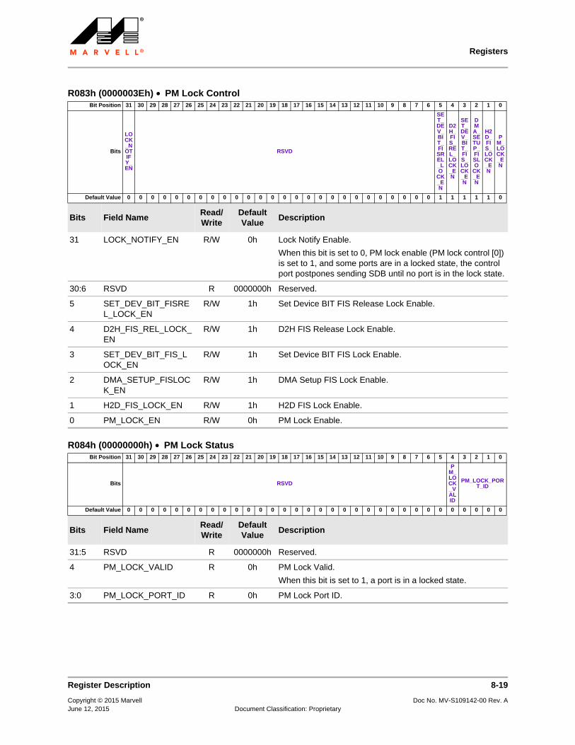
Registers
R083h (0000003Eh) • PM Lock ControlBit Position 31 30 29 28 27 26 25 24 23 22 21 20 19 18 17 16 15 14 13 12 11 10 9 8 7 6 5 4 3 2 1 0
Bits
LOCK_NOTIFY_EN
RSVD
SET_DEV_BIT_FISREL_LO
CK_EN
D2H_FIS_REL_LOCK_EN
SET_DEV_BIT_FIS_LOCK_EN
DMA_SETUP_FISLO
CK_EN
H2D_FIS_LOCK_EN
PM_LOCK_EN
Default Value 0 0 0 0 0 0 0 0 0 0 0 0 0 0 0 0 0 0 0 0 0 0 0 0 0 0 1 1 1 1 1 0
Bits Field NameRead/Write
Default Value
Description
31 LOCK_NOTIFY_EN R/W 0h Lock Notify Enable.
When this bit is set to 0, PM lock enable (PM lock control [0]) is set to 1, and some ports are in a locked state, the control port postpones sending SDB until no port is in the lock state.
30:6 RSVD R 0000000h Reserved.
5 SET_DEV_BIT_FISREL_LOCK_EN
R/W 1h Set Device BIT FIS Release Lock Enable.
4 D2H_FIS_REL_LOCK_EN
R/W 1h D2H FIS Release Lock Enable.
3 SET_DEV_BIT_FIS_LOCK_EN
R/W 1h Set Device BIT FIS Lock Enable.
2 DMA_SETUP_FISLOCK_EN
R/W 1h DMA Setup FIS Lock Enable.
1 H2D_FIS_LOCK_EN R/W 1h H2D FIS Lock Enable.
0 PM_LOCK_EN R/W 0h PM Lock Enable.
R084h (00000000h) • PM Lock StatusBit Position 31 30 29 28 27 26 25 24 23 22 21 20 19 18 17 16 15 14 13 12 11 10 9 8 7 6 5 4 3 2 1 0
Bits RSVD
PM_LOCK_VALID
PM_LOCK_PORT_ID
Default Value 0 0 0 0 0 0 0 0 0 0 0 0 0 0 0 0 0 0 0 0 0 0 0 0 0 0 0 0 0 0 0 0
Bits Field NameRead/Write
Default Value
Description
31:5 RSVD R 0000000h Reserved.
4 PM_LOCK_VALID R 0h PM Lock Valid.
When this bit is set to 1, a port is in a locked state.
3:0 PM_LOCK_PORT_ID R 0h PM Lock Port ID.
Register Description 8-19
Copyright © 2015 Marvell Doc No. MV-S109142-00 Rev. AJune 12, 2015 Document Classification: Proprietary

88SM9705 SATA 6.0 Gbps: 1-to-5 Port MultiplierPreliminary Specifications
R086h (00002C2Bh) • SEMB I2C ControlBit Position 31 30 29 28 27 26 25 24 23 22 21 20 19 18 17 16 15 14 13 12 11 10 9 8 7 6 5 4 3 2 1 0
Bits RSVD
SEMB_INTR
SEMB_WR
SEMB_ADDR SEMB_RD_WR_DATA RS
VDSEP_TWOWIRE_SERIAL_AD
DRSVD
SEMB_TWOWIRE_SERIAL_ADD
Default Value 0 0 0 0 0 0 0 0 0 0 0 0 0 0 0 0 0 0 1 0 1 1 0 0 0 0 1 0 1 0 1 1
Bits Field NameRead/Write
Default Value
Description
31:29 RSVD R 0h Reserved.
28 SEMB_INTR R 0h SEMB Interrupt.
Refer to the Two-Wire Serial IP specification for more detail.
27 SEMB_WR R/W 0h SEMB Register Write.
SEMB_WR, SEMB_ADDR, and SEMB_RD_WR_DATA signals provide an interface for the software to program the Two-Wire Serial register so that the software can control the interface of Two-Wire Serial.
Refer to the Two-Wire Serial IP Specification for more detail.
26:24 SEMB_ADDR R/W 0h SEMB Register Address.
Refer to the Two-Wire Serial IP Specification for more detail.
23:16 SEMB_RD_WR_DATA R/W 00h SEMB Read Write Data.
Refer to the Two-Wire Serial IP Specification for more detail.
15 RSVD R 0h Reserved.
14:8 SEP_TWOWIRE_SERIAL_ADD
R/W 2Ch SEP Two-Wire Serial Address.
7 RSVD R 0h Reserved.
6:0 SEMB_TWOWIRE_SERIAL_ADD
R/W 2Bh SEMB Two-Wire Serial Address.
R087h (00900000h) • SEMB Time-out ValueBit Position 31 30 29 28 27 26 25 24 23 22 21 20 19 18 17 16 15 14 13 12 11 10 9 8 7 6 5 4 3 2 1 0
Bits RSVD SEMB_TO_VAL
Default Value 0 0 0 0 0 0 0 0 1 0 0 1 0 0 0 0 0 0 0 0 0 0 0 0 0 0 0 0 0 0 0 0
Bits Field NameRead/Write
Default Value
Description
31:24 RSVD R 00h Reserved.
23:0 SEMB_TO_VAL R/W 900000h SEMB Time-Out Value.
SEMB time-out occurs when wait time larger than time-out value times cycle time.
8-20 Register Description
Copyright © 2015 Marvell Doc No. MV-S109142-00 Rev. AJune 12, 2015 Document Classification: Proprietary

Registers
R089h (00000000h) • PLL Control 1Bit Position 31 30 29 28 27 26 25 24 23 22 21 20 19 18 17 16 15 14 13 12 11 10 9 8 7 6 5 4 3 2 1 0
Bits RSVD
ANA_GROUP_TESTS
EL
ANA_GRO
UP_GAINX2
ANA_GRO
UP_BYPASS
ANA_GROUP_BG_SE
L
PLL_TEST_MON
PLL_SCC_RESET_EXT
PLL_SCC_FREQ_DIV
PLL_SSC_GAINX2
PLL_SSC_MO
DE
PLL_PU_SSC
PLL_SSC_EN
Default Value 0 0 0 0 0 0 0 0 0 0 0 0 0 0 0 0 0 0 0 0 0 0 0 0 0 0 0 0 0 0 0 0
Bits Field NameRead/Write
Default Value
Description
31 RSVD R/W 0h Reserved.
30:28 ANA_GROUP_TESTSEL
R/W 0h Analog Group Test Select.
27 ANA_GROUP_GAINX2 R/W 0h Analog Group Gain x2.
26 ANA_GROUP_BYPASS
R/W 0h Analog Group Bypass.
25:24 ANA_GROUP_BG_SEL
R/W 0h Analog Group BG_SEL.
23:20 PLL_TEST_MON R/W 0h PLL Test Monitor.
19 PLL_SCC_RESET_EXT
R/W 0h PLL SCC Reset Extend.
18:4 PLL_SCC_FREQ_DIV R/W 0000h PLL SCC Frequency Divider.
3 PLL_SSC_GAINX2 R/W 0h PLL SSC Gain x2.
2 PLL_SSC_MODE R/W 0h PLL SSC Mode.
1 PLL_PU_SSC R/W 0h PLL Power Up SSC.
0 PLL_SSC_EN R/W 0h PLL SSC Enable.
R08Ah (8000003Fh) • PLL Control 2Bit Position 31 30 29 28 27 26 25 24 23 22 21 20 19 18 17 16 15 14 13 12 11 10 9 8 7 6 5 4 3 2 1 0
BitsPU_PLL
RSVD PLL_SSC_RNG RSVD RS
VDRSVD
SYSCLK_EN
SATA_DEV_4_CLK_EN
SATA_DEV_3_CLK_EN
SATA_DEV_2_CLK_EN
SATA_DEV_1_CLK_EN
SATA_DEV_0_CLK_EN
Default Value 1 0 0 0 0 0 0 0 0 0 0 0 0 0 0 0 0 0 0 0 0 0 0 0 0 0 1 1 1 1 1 1
Bits Field NameRead/Write
Default Value
Description
31 PU_PLL R/W 1h Power-Up PLL (Asynchronous Reset).
30 RSVD R/W 0h Reserved.
29:16 PLL_SSC_RNG R/W 0000h PLL SSC Range.
15:8 RSVD R 00h Reserved.
7 RSVD R 0h Reserved.
6 RSVD R 0h Reserved.
Register Description 8-21
Copyright © 2015 Marvell Doc No. MV-S109142-00 Rev. AJune 12, 2015 Document Classification: Proprietary
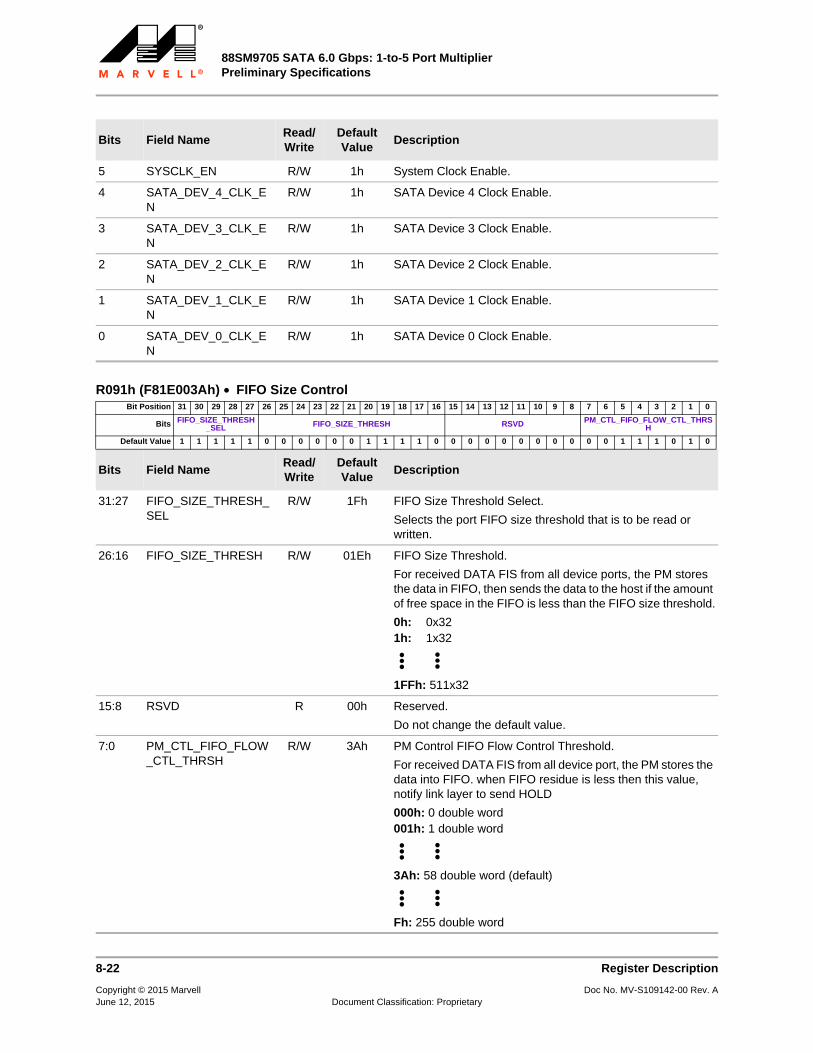
88SM9705 SATA 6.0 Gbps: 1-to-5 Port MultiplierPreliminary Specifications
5 SYSCLK_EN R/W 1h System Clock Enable.
4 SATA_DEV_4_CLK_EN
R/W 1h SATA Device 4 Clock Enable.
3 SATA_DEV_3_CLK_EN
R/W 1h SATA Device 3 Clock Enable.
2 SATA_DEV_2_CLK_EN
R/W 1h SATA Device 2 Clock Enable.
1 SATA_DEV_1_CLK_EN
R/W 1h SATA Device 1 Clock Enable.
0 SATA_DEV_0_CLK_EN
R/W 1h SATA Device 0 Clock Enable.
R091h (F81E003Ah) • FIFO Size ControlBit Position 31 30 29 28 27 26 25 24 23 22 21 20 19 18 17 16 15 14 13 12 11 10 9 8 7 6 5 4 3 2 1 0
Bits FIFO_SIZE_THRESH_SEL FIFO_SIZE_THRESH RSVD PM_CTL_FIFO_FLOW_CTL_THRS
H
Default Value 1 1 1 1 1 0 0 0 0 0 0 1 1 1 1 0 0 0 0 0 0 0 0 0 0 0 1 1 1 0 1 0
Bits Field NameRead/Write
Default Value
Description
31:27 FIFO_SIZE_THRESH_SEL
R/W 1Fh FIFO Size Threshold Select.
Selects the port FIFO size threshold that is to be read or written.
26:16 FIFO_SIZE_THRESH R/W 01Eh FIFO Size Threshold.
For received DATA FIS from all device ports, the PM stores the data in FIFO, then sends the data to the host if the amount of free space in the FIFO is less than the FIFO size threshold.
0h: 0x321h: 1x32
1FFh: 511x32
15:8 RSVD R 00h Reserved.
Do not change the default value.
7:0 PM_CTL_FIFO_FLOW_CTL_THRSH
R/W 3Ah PM Control FIFO Flow Control Threshold.
For received DATA FIS from all device port, the PM stores the data into FIFO. when FIFO residue is less then this value, notify link layer to send HOLD
000h: 0 double word 001h: 1 double word
3Ah: 58 double word (default)
Fh: 255 double word
Bits Field NameRead/Write
Default Value
Description
8-22 Register Description
Copyright © 2015 Marvell Doc No. MV-S109142-00 Rev. AJune 12, 2015 Document Classification: Proprietary
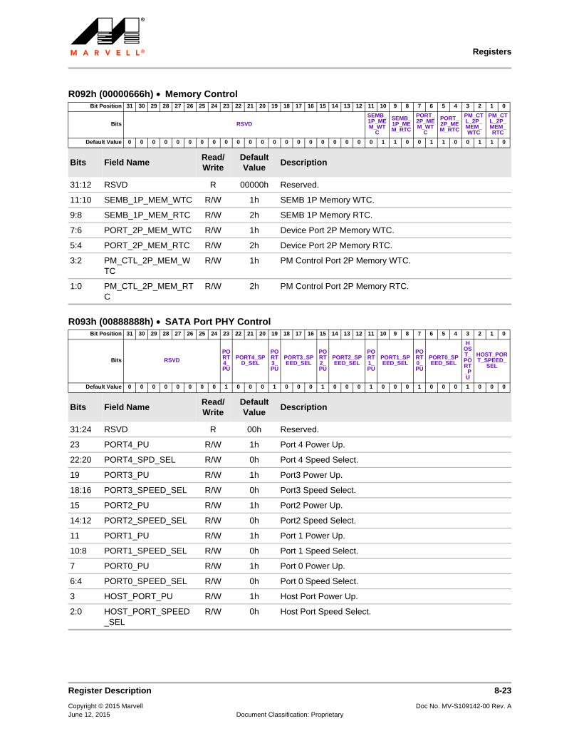
Registers
R092h (00000666h) • Memory ControlBit Position 31 30 29 28 27 26 25 24 23 22 21 20 19 18 17 16 15 14 13 12 11 10 9 8 7 6 5 4 3 2 1 0
Bits RSVD
SEMB_1P_MEM_WT
C
SEMB_1P_MEM_RTC
PORT_2P_MEM_WT
C
PORT_2P_MEM_RTC
PM_CTL_2P_MEM_WTC
PM_CTL_2P_MEM_RTC
Default Value 0 0 0 0 0 0 0 0 0 0 0 0 0 0 0 0 0 0 0 0 0 1 1 0 0 1 1 0 0 1 1 0
Bits Field NameRead/Write
Default Value
Description
31:12 RSVD R 00000h Reserved.
11:10 SEMB_1P_MEM_WTC R/W 1h SEMB 1P Memory WTC.
9:8 SEMB_1P_MEM_RTC R/W 2h SEMB 1P Memory RTC.
7:6 PORT_2P_MEM_WTC R/W 1h Device Port 2P Memory WTC.
5:4 PORT_2P_MEM_RTC R/W 2h Device Port 2P Memory RTC.
3:2 PM_CTL_2P_MEM_WTC
R/W 1h PM Control Port 2P Memory WTC.
1:0 PM_CTL_2P_MEM_RTC
R/W 2h PM Control Port 2P Memory RTC.
R093h (00888888h) • SATA Port PHY ControlBit Position 31 30 29 28 27 26 25 24 23 22 21 20 19 18 17 16 15 14 13 12 11 10 9 8 7 6 5 4 3 2 1 0
Bits RSVD
PORT4_PU
PORT4_SPD_SEL
PORT3_PU
PORT3_SPEED_SEL
PORT2_PU
PORT2_SPEED_SEL
PORT1_PU
PORT1_SPEED_SEL
PORT0_PU
PORT0_SPEED_SEL
HOST_PORT_PU
HOST_PORT_SPEED_
SEL
Default Value 0 0 0 0 0 0 0 0 1 0 0 0 1 0 0 0 1 0 0 0 1 0 0 0 1 0 0 0 1 0 0 0
Bits Field NameRead/Write
Default Value
Description
31:24 RSVD R 00h Reserved.
23 PORT4_PU R/W 1h Port 4 Power Up.
22:20 PORT4_SPD_SEL R/W 0h Port 4 Speed Select.
19 PORT3_PU R/W 1h Port3 Power Up.
18:16 PORT3_SPEED_SEL R/W 0h Port3 Speed Select.
15 PORT2_PU R/W 1h Port2 Power Up.
14:12 PORT2_SPEED_SEL R/W 0h Port2 Speed Select.
11 PORT1_PU R/W 1h Port 1 Power Up.
10:8 PORT1_SPEED_SEL R/W 0h Port 1 Speed Select.
7 PORT0_PU R/W 1h Port 0 Power Up.
6:4 PORT0_SPEED_SEL R/W 0h Port 0 Speed Select.
3 HOST_PORT_PU R/W 1h Host Port Power Up.
2:0 HOST_PORT_SPEED_SEL
R/W 0h Host Port Speed Select.
Register Description 8-23
Copyright © 2015 Marvell Doc No. MV-S109142-00 Rev. AJune 12, 2015 Document Classification: Proprietary

88SM9705 SATA 6.0 Gbps: 1-to-5 Port MultiplierPreliminary Specifications
R0A0h (00000000h) • Side Bank Address Register Bit Position 31 30 29 28 27 26 25 24 23 22 21 20 19 18 17 16 15 14 13 12 11 10 9 8 7 6 5 4 3 2 1 0
Bits
SPI_ME
M_ACCESS
RSVD UNIT_SEL MEM_ADD
Default Value 0 0 0 0 0 0 0 0 0 0 0 0 0 0 0 0 0 0 0 0 0 0 0 0 0 0 0 0 0 0 0 0
Bits Field NameRead/Write
Default Value
Description
31 SPI_MEM_ACCESS R/W 0h Memory Access for SPI.
0h: Other register access.1h: Read SPI memory.
30:28 RSVD R/W 0h Reserved.
Do not change the default value.
27:24 UNIT_SEL R/W 0h Unit Select.
0h: SPI controller register1h: UART controller register
23:0 MEM_ADD R/W 000000h Address for the Memory or Register.
R0A1h (00000000h) • Side Bank Data Register Bit Position 31 30 29 28 27 26 25 24 23 22 21 20 19 18 17 16 15 14 13 12 11 10 9 8 7 6 5 4 3 2 1 0
Bits SIDE_BANK_ACCESS
Default Value 0 0 0 0 0 0 0 0 0 0 0 0 0 0 0 0 0 0 0 0 0 0 0 0 0 0 0 0 0 0 0 0
Bits Field NameRead/Write
Default Value
Description
31:0 SIDE_BANK_ACCESS R/W 00000000h Data Register of Side Bank Access.
8-24 Register Description
Copyright © 2015 Marvell Doc No. MV-S109142-00 Rev. AJune 12, 2015 Document Classification: Proprietary

Registers
8.3.3 Host Port PHY Event Counter Registers
8.3.4 General Purpose Input/Output (GPIO) Registers
R100h (00000000h) • Host Port PHY Event Counter 1 Bit Position 31 30 29 28 27 26 25 24 23 22 21 20 19 18 17 16 15 14 13 12 11 10 9 8 7 6 5 4 3 2 1 0
Bits PHY_EVENT_CNT_1
Default Value 0 0 0 0 0 0 0 0 0 0 0 0 0 0 0 0 0 0 0 0 0 0 0 0 0 0 0 0 0 0 0 0
Bits Field NameRead/Write
Default Value
Description
31:0 PHY_EVENT_CNT_1 R/W 00000000h PHY Event Counter 1.
This register contains both the counter identifier and the counter value:
• Counter identifier: Read-only value 00002C01h.• Counter: 32-bit counter, contains number of signature D2H
register FISes that were transmitted to the host from the control port.
R3A0h (00000000h) • GPIO Data Out Bit Position 31 30 29 28 27 26 25 24 23 22 21 20 19 18 17 16 15 14 13 12 11 10 9 8 7 6 5 4 3 2 1 0
Bits RSVD GPIO[19:0]_DATA_OUTPUT
Default Value 0 0 0 0 0 0 0 0 0 0 0 0 0 0 0 0 0 0 0 0 0 0 0 0 0 0 0 0 0 0 0 0
Bits Field NameRead/Write
Default Value
Description
31:20 RSVD R 000h Reserved.
19:0 GPIO[19:0]_DATA_OUTPUT
R/W 00000h GPIO[19:0] Data Output.
When GPIO is in output mode, modify this register to control the output value.
R3A4h (000107C0h) • GPIO Data Out Enable Bit Position 31 30 29 28 27 26 25 24 23 22 21 20 19 18 17 16 15 14 13 12 11 10 9 8 7 6 5 4 3 2 1 0
Bits
OUTPUT_EN_POLARITY
RSVD GPIO_OUTPUT_EN
Default Value 0 0 0 0 0 0 0 0 0 0 0 0 0 0 0 1 0 0 0 0 0 1 1 1 1 1 0 0 0 0 0 0
Bits Field NameRead/Write
Default Value
Description
31 OUTPUT_EN_POLARITY
R 0h Output Enable Polarity.
0h: Positive1h: NegativeGPIO_OUTPUT_EN (R3A4h [19:0]) is reversed.
30:20 RSVD R 000h Reserved.
Register Description 8-25
Copyright © 2015 Marvell Doc No. MV-S109142-00 Rev. AJune 12, 2015 Document Classification: Proprietary

88SM9705 SATA 6.0 Gbps: 1-to-5 Port MultiplierPreliminary Specifications
19:0 GPIO_OUTPUT_EN R/W 107C0h GPIO Output Enable.
GPIO 6, 7, 8, 9, 10, and 16 are enabled by default.
R3A8h (00000000h) • GPIO Blink Enable Bit Position 31 30 29 28 27 26 25 24 23 22 21 20 19 18 17 16 15 14 13 12 11 10 9 8 7 6 5 4 3 2 1 0
Bits RSVD GPIO[19:11]_BLINKING_EN GPIO[10:5]_BLINKING_DIS
GPIO[4:0]_BLINKING_EN
Default Value 0 0 0 0 0 0 0 0 0 0 0 0 0 0 0 0 0 0 0 0 0 0 0 0 0 0 0 0 0 0 0 0
Bits Field NameRead/Write
Default Value
Description
31:20 RSVD R 000h Reserved.
19:11 GPIO[19:11]_BLINKING_EN
R/W 000h GPIO[19:11] Blinking Enable.
0h: Disable1h: Enable
10:5 GPIO[10:5]_BLINKING_DIS
R/W 00h GPIO[10:5] Blinking Disable.
0h: Enable1h: Disable
4:0 GPIO[4:0]_BLINKING_EN
R/W 00h GPIO[4:0] Blinking Enable.
0h: Disable1h: Enable
R3ACh (00000000h) • GPIO Data In Polarity Bit Position 31 30 29 28 27 26 25 24 23 22 21 20 19 18 17 16 15 14 13 12 11 10 9 8 7 6 5 4 3 2 1 0
Bits RSVD GPIO_DATA_INPUT_POLARITY_BIT_MAP
Default Value 0 0 0 0 0 0 0 0 0 0 0 0 0 0 0 0 0 0 0 0 0 0 0 0 0 0 0 0 0 0 0 0
Bits Field NameRead/Write
Default Value
Description
31:20 RSVD R 000h Reserved.
19:0 GPIO_DATA_INPUT_POLARITY_BIT_MAP
R/W 00000h GPIO Data Input Polarity Bit Map.
0h: Positive polarity1h: Negative polarity
R3B0h (00000000h) • GPIO Data In Bit Position 31 30 29 28 27 26 25 24 23 22 21 20 19 18 17 16 15 14 13 12 11 10 9 8 7 6 5 4 3 2 1 0
Bits RSVD GPIO_INPUT_DATA_BIT_MAP
Default Value 0 0 0 0 0 0 0 0 0 0 0 0 0 0 0 0 0 0 0 0 0 0 0 0 0 0 0 0 0 0 0 0
Bits Field NameRead/Write
Default Value
Description
31:20 RSVD R 000h Reserved.
19:0 GPIO_INPUT_DATA_BIT_MAP
R/W 00000h GPIO Input Data Bit Map.
Bits Field NameRead/Write
Default Value
Description
8-26 Register Description
Copyright © 2015 Marvell Doc No. MV-S109142-00 Rev. AJune 12, 2015 Document Classification: Proprietary
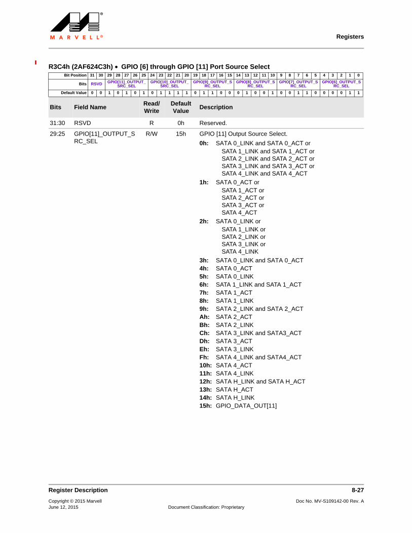
Registers
R3C4h (2AF624C3h) • GPIO [6] through GPIO [11] Port Source Select Bit Position 31 30 29 28 27 26 25 24 23 22 21 20 19 18 17 16 15 14 13 12 11 10 9 8 7 6 5 4 3 2 1 0
Bits RSVD GPIO[11]_OUTPUT_SRC_SEL
GPIO[10]_OUTPUT_SRC_SEL
GPIO[9]_OUTPUT_SRC_SEL
GPIO[8]_OUTPUT_SRC_SEL
GPIO[7]_OUTPUT_SRC_SEL
GPIO[6]_OUTPUT_SRC_SEL
Default Value 0 0 1 0 1 0 1 0 1 1 1 1 0 1 1 0 0 0 1 0 0 1 0 0 1 1 0 0 0 0 1 1
Bits Field NameRead/Write
Default Value
Description
31:30 RSVD R 0h Reserved.
29:25 GPIO[11]_OUTPUT_SRC_SEL
R/W 15h GPIO [11] Output Source Select.
0h: SATA 0_LINK and SATA 0_ACT orSATA 1_LINK and SATA 1_ACT orSATA 2_LINK and SATA 2_ACT orSATA 3_LINK and SATA 3_ACT or SATA 4_LINK and SATA 4_ACT
1h: SATA 0_ACT orSATA 1_ACT or SATA 2_ACT or SATA 3_ACT or SATA 4_ACT
2h: SATA 0_LINK orSATA 1_LINK orSATA 2_LINK orSATA 3_LINK or SATA 4_LINK
3h: SATA 0_LINK and SATA 0_ACT4h: SATA 0_ACT5h: SATA 0_LINK6h: SATA 1_LINK and SATA 1_ACT7h: SATA 1_ACT8h: SATA 1_LINK9h: SATA 2_LINK and SATA 2_ACTAh: SATA 2_ACT Bh: SATA 2_LINK Ch: SATA 3_LINK and SATA3_ACTDh: SATA 3_ACT Eh: SATA 3_LINK Fh: SATA 4_LINK and SATA4_ACT10h: SATA 4_ACT 11h: SATA 4_LINK 12h: SATA H_LINK and SATA H_ACT 13h: SATA H_ACT 14h: SATA H_LINK 15h: GPIO_DATA_OUT[11]
Register Description 8-27
Copyright © 2015 Marvell Doc No. MV-S109142-00 Rev. AJune 12, 2015 Document Classification: Proprietary

88SM9705 SATA 6.0 Gbps: 1-to-5 Port MultiplierPreliminary Specifications
24:20 GPIO[10]_OUTPUT_SRC_SEL
R/W 0Fh GPIO [10] Output Source Select.
0h: SATA 0_LINK and SATA 0_ACT orSATA 1_LINK and SATA 1_ACT orSATA 2_LINK and SATA 2_ACT orSATA 3_LINK and SATA 3_ACT or SATA 4_LINK and SATA 4_ACT
1h: SATA 0_ACT orSATA 1_ACT or SATA 2_ACT or SATA 3_ACT or SATA 4_ACT
2h: SATA 0_LINK orSATA 1_LINK orSATA 2_LINK orSATA 3_LINK or SATA 4_LINK
3h: SATA 0_LINK and SATA 0_ACT4h: SATA 0_ACT5h: SATA 0_LINK6h: SATA 1_LINK and SATA 1_ACT 7h: SATA 1_ACT8h: SATA 1_LINK9h: SATA 2_LINK and SATA 2_ACT Ah: SATA 2_ACT Bh: SATA 2_LINK Ch: SATA 3_LINK and SATA3_ACT Dh: SATA 3_ACT Eh: SATA 3_LINK Fh: SATA 4_LINK and SATA4_ACT 10h: SATA 4_ACT 11h: SATA 4_LINK 12h: SATA H_LINK and SATA H_ACT 13h: SATA H_ACT 14h: SATA H_LINK 15h: GPIO_DATA_OUT[10]
Bits Field NameRead/Write
Default Value
Description
8-28 Register Description
Copyright © 2015 Marvell Doc No. MV-S109142-00 Rev. AJune 12, 2015 Document Classification: Proprietary

Registers
19:15 GPIO[9]_OUTPUT_SRC_SEL
R/W 0Ch GPIO [9] Output Source Select.
0h: SATA 0_LINK and SATA 0_ACT orSATA 1_LINK and SATA 1_ACT orSATA 2_LINK and SATA 2_ACT orSATA 3_LINK and SATA 3_ACT or SATA 4_LINK and SATA 4_ACT
1h: SATA 0_ACT orSATA 1_ACT or SATA 2_ACT or SATA 3_ACT or SATA 4_ACT
2h: SATA 0_LINK orSATA 1_LINK orSATA 2_LINK orSATA 3_LINK or SATA 4_LINK
3h: SATA 0_LINK and SATA 0_ACT4h: SATA 0_ACT5h: SATA 0_LINK6h: SATA 1_LINK and SATA 1_ACT 7h: SATA 1_ACT8h: SATA 1_LINK9h: SATA 2_LINK and SATA 2_ACT Ah: SATA 2_ACT Bh: SATA 2_LINK Ch: SATA 3_LINK and SATA3_ACT Dh: SATA 3_ACT Eh: SATA 3_LINK Fh: SATA 4_LINK and SATA4_ACT 10h: SATA 4_ACT 11h: SATA 4_LINK 12h: SATA H_LINK and SATA H_ACT 13h: SATA H_ACT 14h: SATA H_LINK 15h: GPIO_DATA_OUT[9]
Bits Field NameRead/Write
Default Value
Description
Register Description 8-29
Copyright © 2015 Marvell Doc No. MV-S109142-00 Rev. AJune 12, 2015 Document Classification: Proprietary

88SM9705 SATA 6.0 Gbps: 1-to-5 Port MultiplierPreliminary Specifications
14:10 GPIO[8]_OUTPUT_SRC_SEL
R/W 09h GPIO [8] Output Source Select.
0h: SATA 0_LINK and SATA 0_ACT orSATA 1_LINK and SATA 1_ACT orSATA 2_LINK and SATA 2_ACT orSATA 3_LINK and SATA 3_ACT or SATA 4_LINK and SATA 4_ACT
1h: SATA 0_ACT orSATA 1_ACT or SATA 2_ACT or SATA 3_ACT or SATA 4_ACT
2h: SATA 0_LINK orSATA 1_LINK orSATA 2_LINK orSATA 3_LINK or SATA 4_LINK
3h: SATA 0_LINK and SATA 0_ACT4h: SATA 0_ACT5h: SATA 0_LINK6h: SATA 1_LINK and SATA 1_ACT 7h: SATA 1_ACT8h: SATA 1_LINK9h: SATA 2_LINK and SATA 2_ACT Ah: SATA 2_ACT Bh: SATA 2_LINK Ch: SATA 3_LINK and SATA3_ACT Dh: SATA 3_ACT Eh: SATA 3_LINK Fh: SATA 4_LINK and SATA4_ACT 10h: SATA 4_ACT 11h: SATA 4_LINK 12h: SATA H_LINK and SATA H_ACT 13h: SATA H_ACT 14h: SATA H_LINK 15h: GPIO_DATA_OUT[8]
Bits Field NameRead/Write
Default Value
Description
8-30 Register Description
Copyright © 2015 Marvell Doc No. MV-S109142-00 Rev. AJune 12, 2015 Document Classification: Proprietary

Registers
9:5 GPIO[7]_OUTPUT_SRC_SEL
R/W 06h GPIO [7] Output Source Select.
0h: SATA 0_LINK and SATA 0_ACT orSATA 1_LINK and SATA 1_ACT orSATA 2_LINK and SATA 2_ACT orSATA 3_LINK and SATA 3_ACT or SATA 4_LINK and SATA 4_ACT
1h: SATA 0_ACT orSATA 1_ACT or SATA 2_ACT or SATA 3_ACT or SATA 4_ACT
2h: SATA 0_LINK orSATA 1_LINK orSATA 2_LINK orSATA 3_LINK or SATA 4_LINK
3h: SATA 0_LINK and SATA 0_ACT4h: SATA 0_ACT5h: SATA 0_LINK6h: SATA 1_LINK and SATA 1_ACT 7h: SATA 1_ACT8h: SATA 1_LINK9h: SATA 2_LINK and SATA 2_ACT Ah: SATA 2_ACT Bh: SATA 2_LINK Ch: SATA 3_LINK and SATA3_ACT Dh: SATA 3_ACT Eh: SATA 3_LINKFh: SATA 4_LINK and SATA4_ACT 10h: SATA 4_ACT 11h: SATA 4_LINK 12h: SATA H_LINK and SATA H_ACT 13h: SATA H_ACT 14h: SATA H_LINK 15h: GPIO_DATA_OUT[7]
Bits Field NameRead/Write
Default Value
Description
Register Description 8-31
Copyright © 2015 Marvell Doc No. MV-S109142-00 Rev. AJune 12, 2015 Document Classification: Proprietary

88SM9705 SATA 6.0 Gbps: 1-to-5 Port MultiplierPreliminary Specifications
4:0 GPIO[6]_OUTPUT_SRC_SEL
R/W 03h GPIO [6] Output Source Select.
0h: SATA 0_LINK and SATA 0_ACT orSATA 1_LINK and SATA 1_ACT orSATA 2_LINK and SATA 2_ACT orSATA 3_LINK and SATA 3_ACT or SATA 4_LINK and SATA 4_ACT
1h: SATA 0_ACT orSATA 1_ACT or SATA 2_ACT or SATA 3_ACT or SATA 4_ACT
2h: SATA 0_LINK orSATA 1_LINK orSATA 2_LINK orSATA 3_LINK or SATA 4_LINK
3h: SATA 0_LINK and SATA 0_ACT4h: SATA 0_ACT5h: SATA 0_LINK6h: SATA 1_LINK and SATA 1_ACT 7h: SATA 1_ACT8h: SATA 1_LINK9h: SATA 2_LINK and SATA 2_ACT Ah: SATA 2_ACT Bh: SATA 2_LINK Ch: SATA 3_LINK and SATA3_ACT Dh: SATA 3_ACT Eh: SATA 3_LINK Fh: SATA 4_LINK and SATA4_ACT 10h: SATA 4_ACT 11h: SATA 4_LINK 12h: SATA H_LINK and SATA H_ACT 13h: SATA H_ACT 14h: SATA H_LINK 15h: GPIO_DATA_OUT[6]
R3C8h (047868C0h) • Power-Control Logic Time-Out Control Register Bit Position 31 30 29 28 27 26 25 24 23 22 21 20 19 18 17 16 15 14 13 12 11 10 9 8 7 6 5 4 3 2 1 0
Bits RSVD TIMEOUT_CNTR_VAL
Default Value 0 0 0 0 0 1 0 0 0 1 1 1 1 0 0 0 0 1 1 0 1 0 0 0 1 1 0 0 0 0 0 0
Bits Field NameRead/Write
Default Value
Description
31:29 RSVD R 0h Reserved.
28:0 TIMEOUT_CNTR_VAL R/W 047868C0h Time-out Counter Value.
The time-out counter value based on 25 MHz clock.
Bits Field NameRead/Write
Default Value
Description
8-32 Register Description
Copyright © 2015 Marvell Doc No. MV-S109142-00 Rev. AJune 12, 2015 Document Classification: Proprietary
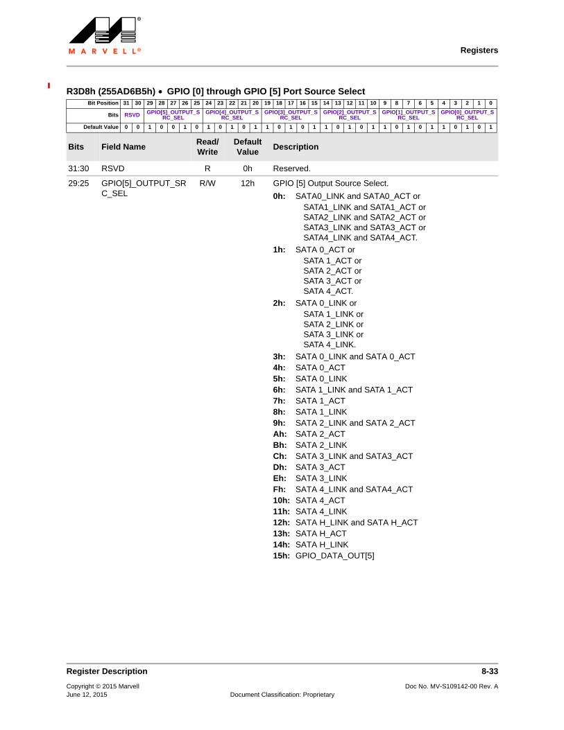
Registers
R3D8h (255AD6B5h) • GPIO [0] through GPIO [5] Port Source Select Bit Position 31 30 29 28 27 26 25 24 23 22 21 20 19 18 17 16 15 14 13 12 11 10 9 8 7 6 5 4 3 2 1 0
Bits RSVD GPIO[5]_OUTPUT_SRC_SEL
GPIO[4]_OUTPUT_SRC_SEL
GPIO[3]_OUTPUT_SRC_SEL
GPIO[2]_OUTPUT_SRC_SEL
GPIO[1]_OUTPUT_SRC_SEL
GPIO[0]_OUTPUT_SRC_SEL
Default Value 0 0 1 0 0 1 0 1 0 1 0 1 1 0 1 0 1 1 0 1 0 1 1 0 1 0 1 1 0 1 0 1
Bits Field NameRead/Write
Default Value
Description
31:30 RSVD R 0h Reserved.
29:25 GPIO[5]_OUTPUT_SRC_SEL
R/W 12h GPIO [5] Output Source Select.
0h: SATA0_LINK and SATA0_ACT orSATA1_LINK and SATA1_ACT orSATA2_LINK and SATA2_ACT orSATA3_LINK and SATA3_ACT orSATA4_LINK and SATA4_ACT.
1h: SATA 0_ACT orSATA 1_ACT or SATA 2_ACT or SATA 3_ACT or SATA 4_ACT.
2h: SATA 0_LINK orSATA 1_LINK orSATA 2_LINK orSATA 3_LINK or SATA 4_LINK.
3h: SATA 0_LINK and SATA 0_ACT4h: SATA 0_ACT5h: SATA 0_LINK6h: SATA 1_LINK and SATA 1_ACT 7h: SATA 1_ACT8h: SATA 1_LINK9h: SATA 2_LINK and SATA 2_ACT Ah: SATA 2_ACT Bh: SATA 2_LINK Ch: SATA 3_LINK and SATA3_ACT Dh: SATA 3_ACT Eh: SATA 3_LINK Fh: SATA 4_LINK and SATA4_ACT 10h: SATA 4_ACT 11h: SATA 4_LINK 12h: SATA H_LINK and SATA H_ACT 13h: SATA H_ACT 14h: SATA H_LINK 15h: GPIO_DATA_OUT[5]
Register Description 8-33
Copyright © 2015 Marvell Doc No. MV-S109142-00 Rev. AJune 12, 2015 Document Classification: Proprietary
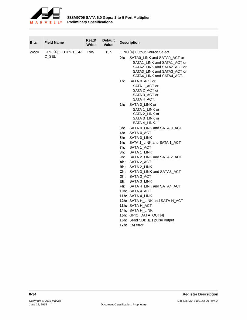
88SM9705 SATA 6.0 Gbps: 1-to-5 Port MultiplierPreliminary Specifications
24:20 GPIO[4]_OUTPUT_SRC_SEL
R/W 15h GPIO [4] Output Source Select.
0h: SATA0_LINK and SATA0_ACT orSATA1_LINK and SATA1_ACT orSATA2_LINK and SATA2_ACT orSATA3_LINK and SATA3_ACT orSATA4_LINK and SATA4_ACT.
1h: SATA 0_ACT orSATA 1_ACT or SATA 2_ACT or SATA 3_ACT or SATA 4_ACT.
2h: SATA 0_LINK orSATA 1_LINK orSATA 2_LINK orSATA 3_LINK or SATA 4_LINK.
3h: SATA 0_LINK and SATA 0_ACT4h: SATA 0_ACT5h: SATA 0_LINK6h: SATA 1_LINK and SATA 1_ACT 7h: SATA 1_ACT8h: SATA 1_LINK9h: SATA 2_LINK and SATA 2_ACT Ah: SATA 2_ACT Bh: SATA 2_LINK Ch: SATA 3_LINK and SATA3_ACT Dh: SATA 3_ACT Eh: SATA 3_LINK Fh: SATA 4_LINK and SATA4_ACT 10h: SATA 4_ACT 11h: SATA 4_LINK 12h: SATA H_LINK and SATA H_ACT 13h: SATA H_ACT 14h: SATA H_LINK 15h: GPIO_DATA_OUT[4]16h: Send SDB 1µs pulse output17h: EM error
Bits Field NameRead/Write
Default Value
Description
8-34 Register Description
Copyright © 2015 Marvell Doc No. MV-S109142-00 Rev. AJune 12, 2015 Document Classification: Proprietary

Registers
19:15 GPIO[3]_OUTPUT_SRC_SEL
R/W 15h GPIO [3] Output Source Select.
0h: SATA0_LINK and SATA0_ACT orSATA1_LINK and SATA1_ACT orSATA2_LINK and SATA2_ACT orSATA3_LINK and SATA3_ACT orSATA4_LINK and SATA4_ACT.
1h: SATA 0_ACT orSATA 1_ACT or SATA 2_ACT or SATA 3_ACT or SATA 4_ACT.
2h: SATA 0_LINK orSATA 1_LINK orSATA 2_LINK orSATA 3_LINK or SATA 4_LINK.
3h: SATA 0_LINK and SATA 0_ACT4h: SATA 0_ACT5h: SATA 0_LINK6h: SATA 1_LINK and SATA 1_ACT 7h: SATA 1_ACT8h: SATA 1_LINK9h: SATA 2_LINK and SATA 2_ACT Ah: SATA 2_ACT Bh: SATA 2_LINK Ch: SATA 3_LINK and SATA3_ACT Dh: SATA 3_ACT Eh: SATA 3_LINK Fh: SATA 4_LINK and SATA4_ACT 10h: SATA 4_ACT 11h: SATA 4_LINK 12h: SATA H_LINK and SATA H_ACT 13h: SATA H_ACT 14h: SATA H_LINK 15h: GPIO_DATA_OUT[3]
Bits Field NameRead/Write
Default Value
Description
Register Description 8-35
Copyright © 2015 Marvell Doc No. MV-S109142-00 Rev. AJune 12, 2015 Document Classification: Proprietary

88SM9705 SATA 6.0 Gbps: 1-to-5 Port MultiplierPreliminary Specifications
14:10 GPIO[2]_OUTPUT_SRC_SEL
R/W 15h GPIO [2] Output Source Select.
0h: SATA0_LINK and SATA0_ACT orSATA1_LINK and SATA1_ACT orSATA2_LINK and SATA2_ACT orSATA3_LINK and SATA3_ACT orSATA4_LINK and SATA4_ACT.
1h: SATA 0_ACT orSATA 1_ACT or SATA 2_ACT or SATA 3_ACT or SATA 4_ACT.
2h: SATA 0_LINK orSATA 1_LINK orSATA 2_LINK orSATA 3_LINK or SATA 4_LINK.
3h: SATA 0_LINK and SATA 0_ACT4h: SATA 0_ACT5h: SATA 0_LINK6h: SATA 1_LINK and SATA 1_ACT 7h: SATA 1_ACT8h: SATA 1_LINK9h: SATA 2_LINK and SATA 2_ACT Ah: SATA 2_ACT Bh: SATA 2_LINK Ch: SATA 3_LINK and SATA3_ACT Dh: SATA 3_ACT Eh: SATA 3_LINK Fh: SATA 4_LINK and SATA4_ACT 10h: SATA 4_ACT 11h: SATA 4_LINK 12h: SATA H_LINK and SATA H_ACT 13h: SATA H_ACT 14h: SATA H_LINK 15h: GPIO_DATA_OUT[2]
Bits Field NameRead/Write
Default Value
Description
8-36 Register Description
Copyright © 2015 Marvell Doc No. MV-S109142-00 Rev. AJune 12, 2015 Document Classification: Proprietary
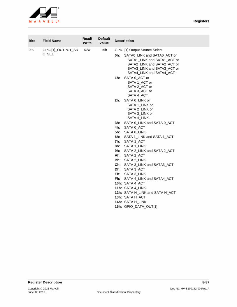
Registers
9:5 GPIO[1]_OUTPUT_SRC_SEL
R/W 15h GPIO [1] Output Source Select.
0h: SATA0_LINK and SATA0_ACT orSATA1_LINK and SATA1_ACT orSATA2_LINK and SATA2_ACT orSATA3_LINK and SATA3_ACT orSATA4_LINK and SATA4_ACT.
1h: SATA 0_ACT orSATA 1_ACT or SATA 2_ACT or SATA 3_ACT or SATA 4_ACT.
2h: SATA 0_LINK orSATA 1_LINK orSATA 2_LINK orSATA 3_LINK or SATA 4_LINK.
3h: SATA 0_LINK and SATA 0_ACT4h: SATA 0_ACT5h: SATA 0_LINK6h: SATA 1_LINK and SATA 1_ACT 7h: SATA 1_ACT8h: SATA 1_LINK9h: SATA 2_LINK and SATA 2_ACT Ah: SATA 2_ACT Bh: SATA 2_LINK Ch: SATA 3_LINK and SATA3_ACT Dh: SATA 3_ACT Eh: SATA 3_LINK Fh: SATA 4_LINK and SATA4_ACT 10h: SATA 4_ACT 11h: SATA 4_LINK 12h: SATA H_LINK and SATA H_ACT 13h: SATA H_ACT 14h: SATA H_LINK 15h: GPIO_DATA_OUT[1]
Bits Field NameRead/Write
Default Value
Description
Register Description 8-37
Copyright © 2015 Marvell Doc No. MV-S109142-00 Rev. AJune 12, 2015 Document Classification: Proprietary

88SM9705 SATA 6.0 Gbps: 1-to-5 Port MultiplierPreliminary Specifications
4:0 GPIO[0]_OUTPUT_SRC_SEL
R/W 15h GPIO [0] Output Source Select.
0h: SATA0_LINK and SATA0_ACT orSATA1_LINK and SATA1_ACT orSATA2_LINK and SATA2_ACT orSATA3_LINK and SATA3_ACT orSATA4_LINK and SATA4_ACT.
1h: SATA 0_ACT orSATA 1_ACT or SATA 2_ACT or SATA 3_ACT or SATA 4_ACT.
2h: SATA 0_LINK orSATA 1_LINK orSATA 2_LINK orSATA 3_LINK or SATA 4_LINK.
3h: SATA 0_LINK and SATA 0_ACT4h: SATA 0_ACT5h: SATA 0_LINK6h: SATA 1_LINK and SATA 1_ACT 7h: SATA 1_ACT8h: SATA 1_LINK9h: SATA 2_LINK and SATA 2_ACT Ah: SATA 2_ACT Bh: SATA 2_LINK Ch: SATA 3_LINK and SATA3_ACT Dh: SATA 3_ACT Eh: SATA 3_LINK Fh: SATA 4_LINK and SATA4_ACT 10h: SATA 4_ACT 11h: SATA 4_LINK 12h: SATA H_LINK and SATA H_ACT 13h: SATA H_ACT 14h: SATA H_LINK 15h: GPIO_DATA_OUT[0]
Bits Field NameRead/Write
Default Value
Description
8-38 Register Description
Copyright © 2015 Marvell Doc No. MV-S109142-00 Rev. AJune 12, 2015 Document Classification: Proprietary
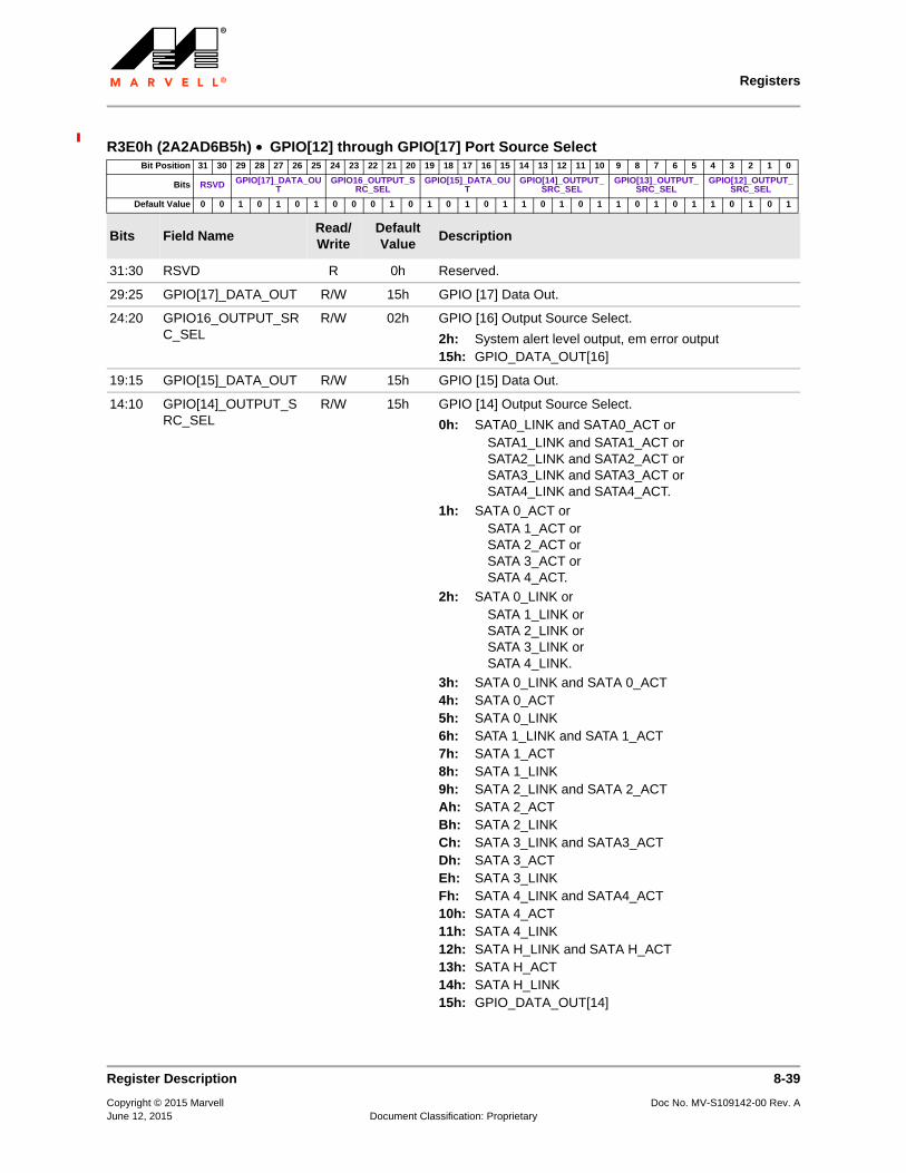
Registers
R3E0h (2A2AD6B5h) • GPIO[12] through GPIO[17] Port Source Select Bit Position 31 30 29 28 27 26 25 24 23 22 21 20 19 18 17 16 15 14 13 12 11 10 9 8 7 6 5 4 3 2 1 0
Bits RSVD GPIO[17]_DATA_OUT
GPIO16_OUTPUT_SRC_SEL
GPIO[15]_DATA_OUT
GPIO[14]_OUTPUT_SRC_SEL
GPIO[13]_OUTPUT_SRC_SEL
GPIO[12]_OUTPUT_SRC_SEL
Default Value 0 0 1 0 1 0 1 0 0 0 1 0 1 0 1 0 1 1 0 1 0 1 1 0 1 0 1 1 0 1 0 1
Bits Field NameRead/Write
Default Value
Description
31:30 RSVD R 0h Reserved.
29:25 GPIO[17]_DATA_OUT R/W 15h GPIO [17] Data Out.
24:20 GPIO16_OUTPUT_SRC_SEL
R/W 02h GPIO [16] Output Source Select.
2h: System alert level output, em error output15h: GPIO_DATA_OUT[16]
19:15 GPIO[15]_DATA_OUT R/W 15h GPIO [15] Data Out.
14:10 GPIO[14]_OUTPUT_SRC_SEL
R/W 15h GPIO [14] Output Source Select.
0h: SATA0_LINK and SATA0_ACT orSATA1_LINK and SATA1_ACT orSATA2_LINK and SATA2_ACT orSATA3_LINK and SATA3_ACT orSATA4_LINK and SATA4_ACT.
1h: SATA 0_ACT orSATA 1_ACT or SATA 2_ACT or SATA 3_ACT or SATA 4_ACT.
2h: SATA 0_LINK orSATA 1_LINK orSATA 2_LINK orSATA 3_LINK or SATA 4_LINK.
3h: SATA 0_LINK and SATA 0_ACT4h: SATA 0_ACT5h: SATA 0_LINK6h: SATA 1_LINK and SATA 1_ACT 7h: SATA 1_ACT8h: SATA 1_LINK9h: SATA 2_LINK and SATA 2_ACT Ah: SATA 2_ACT Bh: SATA 2_LINK Ch: SATA 3_LINK and SATA3_ACT Dh: SATA 3_ACT Eh: SATA 3_LINK Fh: SATA 4_LINK and SATA4_ACT 10h: SATA 4_ACT 11h: SATA 4_LINK 12h: SATA H_LINK and SATA H_ACT 13h: SATA H_ACT 14h: SATA H_LINK 15h: GPIO_DATA_OUT[14]
Register Description 8-39
Copyright © 2015 Marvell Doc No. MV-S109142-00 Rev. AJune 12, 2015 Document Classification: Proprietary
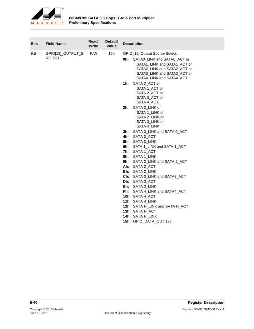
88SM9705 SATA 6.0 Gbps: 1-to-5 Port MultiplierPreliminary Specifications
9:5 GPIO[13]_OUTPUT_SRC_SEL
R/W 15h GPIO [13] Output Source Select.
0h: SATA0_LINK and SATA0_ACT orSATA1_LINK and SATA1_ACT orSATA2_LINK and SATA2_ACT orSATA3_LINK and SATA3_ACT orSATA4_LINK and SATA4_ACT.
1h: SATA 0_ACT orSATA 1_ACT or SATA 2_ACT or SATA 3_ACT or SATA 4_ACT.
2h: SATA 0_LINK orSATA 1_LINK orSATA 2_LINK orSATA 3_LINK or SATA 4_LINK.
3h: SATA 0_LINK and SATA 0_ACT4h: SATA 0_ACT5h: SATA 0_LINK6h: SATA 1_LINK and SATA 1_ACT 7h: SATA 1_ACT8h: SATA 1_LINK9h: SATA 2_LINK and SATA 2_ACT Ah: SATA 2_ACT Bh: SATA 2_LINK Ch: SATA 3_LINK and SATA3_ACT Dh: SATA 3_ACT Eh: SATA 3_LINK Fh: SATA 4_LINK and SATA4_ACT 10h: SATA 4_ACT 11h: SATA 4_LINK 12h: SATA H_LINK and SATA H_ACT 13h: SATA H_ACT 14h: SATA H_LINK 15h: GPIO_DATA_OUT[13]
Bits Field NameRead/Write
Default Value
Description
8-40 Register Description
Copyright © 2015 Marvell Doc No. MV-S109142-00 Rev. AJune 12, 2015 Document Classification: Proprietary

Registers
4:0 GPIO[12]_OUTPUT_SRC_SEL
R/W 15h GPIO [12] Output Source Select.
0h: SATA0_LINK and SATA0_ACT orSATA1_LINK and SATA1_ACT orSATA2_LINK and SATA2_ACT orSATA3_LINK and SATA3_ACT orSATA4_LINK and SATA4_ACT.
1h: SATA 0_ACT orSATA 1_ACT or SATA 2_ACT or SATA 3_ACT or SATA 4_ACT.
2h: SATA 0_LINK orSATA 1_LINK orSATA 2_LINK orSATA 3_LINK or SATA 4_LINK.
3h: SATA 0_LINK and SATA 0_ACT4h: SATA 0_ACT5h: SATA 0_LINK6h: SATA 1_LINK and SATA 1_ACT 7h: SATA 1_ACT8h: SATA 1_LINK9h: SATA 2_LINK and SATA 2_ACT Ah: SATA 2_ACT Bh: SATA 2_LINK Ch: SATA 3_LINK and SATA3_ACT Dh: SATA 3_ACT Eh: SATA 3_LINK Fh: SATA 4_LINK and SATA4_ACT 10h: SATA 4_ACT 11h: SATA 4_LINK 12h: SATA H_LINK and SATA H_ACT 13h: SATA H_ACT 14h: SATA H_LINK 15h: GPIO_DATA_OUT[12]
Bits Field NameRead/Write
Default Value
Description
Register Description 8-41
Copyright © 2015 Marvell Doc No. MV-S109142-00 Rev. AJune 12, 2015 Document Classification: Proprietary
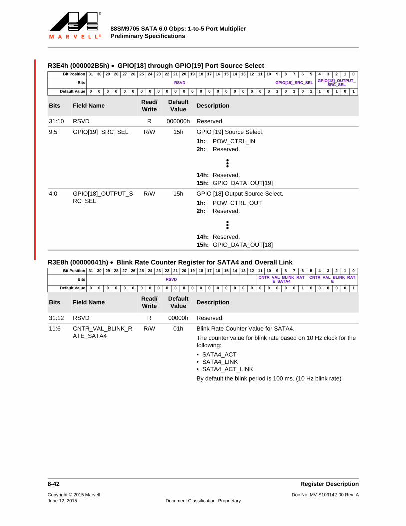
88SM9705 SATA 6.0 Gbps: 1-to-5 Port MultiplierPreliminary Specifications
R3E4h (000002B5h) • GPIO[18] through GPIO[19] Port Source Select Bit Position 31 30 29 28 27 26 25 24 23 22 21 20 19 18 17 16 15 14 13 12 11 10 9 8 7 6 5 4 3 2 1 0
Bits RSVD GPIO[19]_SRC_SEL GPIO[18]_OUTPUT_SRC_SEL
Default Value 0 0 0 0 0 0 0 0 0 0 0 0 0 0 0 0 0 0 0 0 0 0 1 0 1 0 1 1 0 1 0 1
Bits Field NameRead/Write
Default Value
Description
31:10 RSVD R 000000h Reserved.
9:5 GPIO[19]_SRC_SEL R/W 15h GPIO [19] Source Select.
1h: POW_CTRL_IN2h: Reserved.
14h: Reserved.15h: GPIO_DATA_OUT[19]
4:0 GPIO[18]_OUTPUT_SRC_SEL
R/W 15h GPIO [18] Output Source Select.
1h: POW_CTRL_OUT2h: Reserved.
14h: Reserved.15h: GPIO_DATA_OUT[18]
R3E8h (00000041h) • Blink Rate Counter Register for SATA4 and Overall Link Bit Position 31 30 29 28 27 26 25 24 23 22 21 20 19 18 17 16 15 14 13 12 11 10 9 8 7 6 5 4 3 2 1 0
Bits RSVD CNTR_VAL_BLINK_RATE_SATA4
CNTR_VAL_BLINK_RATE
Default Value 0 0 0 0 0 0 0 0 0 0 0 0 0 0 0 0 0 0 0 0 0 0 0 0 0 1 0 0 0 0 0 1
Bits Field NameRead/Write
Default Value
Description
31:12 RSVD R 00000h Reserved.
11:6 CNTR_VAL_BLINK_RATE_SATA4
R/W 01h Blink Rate Counter Value for SATA4.
The counter value for blink rate based on 10 Hz clock for the following:
• SATA4_ACT• SATA4_LINK• SATA4_ACT_LINK
By default the blink period is 100 ms. (10 Hz blink rate)
8-42 Register Description
Copyright © 2015 Marvell Doc No. MV-S109142-00 Rev. AJune 12, 2015 Document Classification: Proprietary
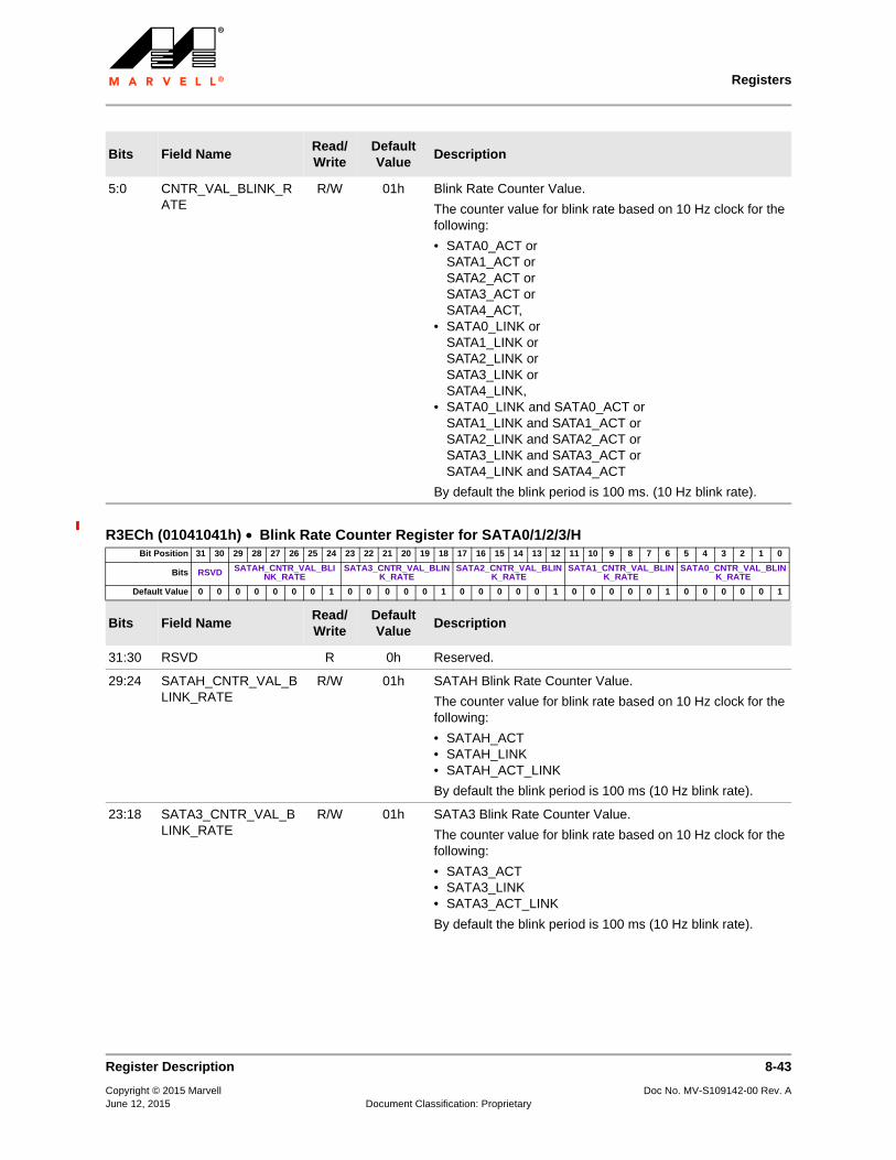
Registers
5:0 CNTR_VAL_BLINK_RATE
R/W 01h Blink Rate Counter Value.
The counter value for blink rate based on 10 Hz clock for the following:
• SATA0_ACT orSATA1_ACT orSATA2_ACT orSATA3_ACT orSATA4_ACT,
• SATA0_LINK orSATA1_LINK orSATA2_LINK orSATA3_LINK orSATA4_LINK,
• SATA0_LINK and SATA0_ACT orSATA1_LINK and SATA1_ACT orSATA2_LINK and SATA2_ACT orSATA3_LINK and SATA3_ACT orSATA4_LINK and SATA4_ACT
By default the blink period is 100 ms. (10 Hz blink rate).
R3ECh (01041041h) • Blink Rate Counter Register for SATA0/1/2/3/H Bit Position 31 30 29 28 27 26 25 24 23 22 21 20 19 18 17 16 15 14 13 12 11 10 9 8 7 6 5 4 3 2 1 0
Bits RSVD SATAH_CNTR_VAL_BLINK_RATE
SATA3_CNTR_VAL_BLINK_RATE
SATA2_CNTR_VAL_BLINK_RATE
SATA1_CNTR_VAL_BLINK_RATE
SATA0_CNTR_VAL_BLINK_RATE
Default Value 0 0 0 0 0 0 0 1 0 0 0 0 0 1 0 0 0 0 0 1 0 0 0 0 0 1 0 0 0 0 0 1
Bits Field NameRead/Write
Default Value
Description
31:30 RSVD R 0h Reserved.
29:24 SATAH_CNTR_VAL_BLINK_RATE
R/W 01h SATAH Blink Rate Counter Value.
The counter value for blink rate based on 10 Hz clock for the following:
• SATAH_ACT• SATAH_LINK• SATAH_ACT_LINK
By default the blink period is 100 ms (10 Hz blink rate).
23:18 SATA3_CNTR_VAL_BLINK_RATE
R/W 01h SATA3 Blink Rate Counter Value.
The counter value for blink rate based on 10 Hz clock for the following:
• SATA3_ACT• SATA3_LINK• SATA3_ACT_LINK
By default the blink period is 100 ms (10 Hz blink rate).
Bits Field NameRead/Write
Default Value
Description
Register Description 8-43
Copyright © 2015 Marvell Doc No. MV-S109142-00 Rev. AJune 12, 2015 Document Classification: Proprietary

88SM9705 SATA 6.0 Gbps: 1-to-5 Port MultiplierPreliminary Specifications
17:12 SATA2_CNTR_VAL_BLINK_RATE
R/W 01h SATA2 Blink Rate Counter Value.
The counter value for blink rate based on 10 Hz clock for the following:
• SATA2_ACT• SATA2_LINK• SATA2_ACT_LINK
By default the blink period is 100 ms. (10 Hz blink rate)
11:6 SATA1_CNTR_VAL_BLINK_RATE
R/W 01h SATA1 Blink Rate Counter Value.
The counter value for blink rate based on 10 Hz clock for the following:
• SATA1_ACT• SATA1_LINK• SATA1_ACT_LINK
By default the blink period is 100 ms. (10 Hz blink rate)
5:0 SATA0_CNTR_VAL_BLINK_RATE
R/W 01h SATA0 Blink Rate Counter Value.
The counter value for blink rate based on 10Hz clock for the following:
• SATA0_ACT• SATA0_LINK• SATA0_ACT_LINK
By default the blink period is 100 ms. (10 Hz blink rate)
R3F0h (01041041h) • Blink Rate Counter Register for GPIO_OUT[4] through GPIO_OUT[0] Bit Position 31 30 29 28 27 26 25 24 23 22 21 20 19 18 17 16 15 14 13 12 11 10 9 8 7 6 5 4 3 2 1 0
Bits RSVD GPIO[4]_CNTR_VAL_BLINK_RATE
GPIO[3]_CNTR_VAL_BLINK_RATE
GPIO[2]_CNTR_VAL_BLINK_RATE
GPIO[1]_CNTR_VAL_BLINK_RATE
GPIO[0]_CNTR_VAL_BLINK_RATE
Default Value 0 0 0 0 0 0 0 1 0 0 0 0 0 1 0 0 0 0 0 1 0 0 0 0 0 1 0 0 0 0 0 1
Bits Field NameRead/Write
Default Value
Description
31:30 RSVD R 0h Reserved.
29:24 GPIO[4]_CNTR_VAL_BLINK_RATE
R/W 01h GPIO_OUT[4] Counter Value Blink Rate.
This field indicates the counter value for GPIO_OUT[4] blink rate based on 10Hz clock. By default the blink period is 100 ms. (10 Hz blink rate).
23:18 GPIO[3]_CNTR_VAL_BLINK_RATE
R/W 01h GPIO_OUT[3] Counter Value Blink Rate.
This field indicates the counter value for GPIO_OUT[3] blink rate based on 10Hz clock. By default the blink period is 100 ms. (10 Hz blink rate).
17:12 GPIO[2]_CNTR_VAL_BLINK_RATE
R/W 01h GPIO_OUT[2] Counter Value Blink Rate.
This field indicates the counter value for GPIO_OUT[2] blink rate based on 10 Hz clock. By default the blink period is 100 ms. (10 Hz blink rate).
Bits Field NameRead/Write
Default Value
Description
8-44 Register Description
Copyright © 2015 Marvell Doc No. MV-S109142-00 Rev. AJune 12, 2015 Document Classification: Proprietary
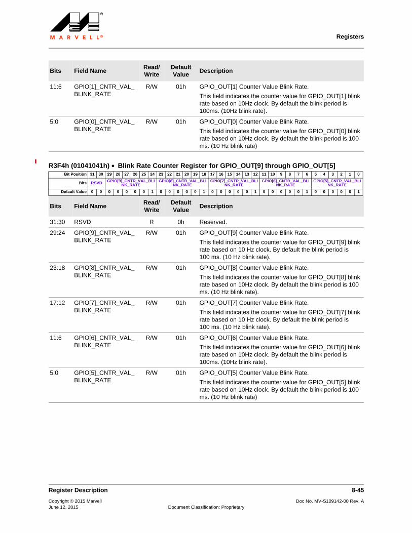
Registers
11:6 GPIO[1]_CNTR_VAL_BLINK_RATE
R/W 01h GPIO_OUT[1] Counter Value Blink Rate.
This field indicates the counter value for GPIO_OUT[1] blink rate based on 10Hz clock. By default the blink period is 100ms. (10Hz blink rate).
5:0 GPIO[0]_CNTR_VAL_BLINK_RATE
R/W 01h GPIO_OUT[0] Counter Value Blink Rate.
This field indicates the counter value for GPIO_OUT[0] blink rate based on 10Hz clock. By default the blink period is 100 ms. (10 Hz blink rate)
R3F4h (01041041h) • Blink Rate Counter Register for GPIO_OUT[9] through GPIO_OUT[5] Bit Position 31 30 29 28 27 26 25 24 23 22 21 20 19 18 17 16 15 14 13 12 11 10 9 8 7 6 5 4 3 2 1 0
Bits RSVD GPIO[9]_CNTR_VAL_BLINK_RATE
GPIO[8]_CNTR_VAL_BLINK_RATE
GPIO[7]_CNTR_VAL_BLINK_RATE
GPIO[6]_CNTR_VAL_BLINK_RATE
GPIO[5]_CNTR_VAL_BLINK_RATE
Default Value 0 0 0 0 0 0 0 1 0 0 0 0 0 1 0 0 0 0 0 1 0 0 0 0 0 1 0 0 0 0 0 1
Bits Field NameRead/Write
Default Value
Description
31:30 RSVD R 0h Reserved.
29:24 GPIO[9]_CNTR_VAL_BLINK_RATE
R/W 01h GPIO_OUT[9] Counter Value Blink Rate.
This field indicates the counter value for GPIO_OUT[9] blink rate based on 10 Hz clock. By default the blink period is 100 ms. (10 Hz blink rate).
23:18 GPIO[8]_CNTR_VAL_BLINK_RATE
R/W 01h GPIO_OUT[8] Counter Value Blink Rate.
This field indicates the counter value for GPIO_OUT[8] blink rate based on 10Hz clock. By default the blink period is 100 ms. (10 Hz blink rate).
17:12 GPIO[7]_CNTR_VAL_BLINK_RATE
R/W 01h GPIO_OUT[7] Counter Value Blink Rate.
This field indicates the counter value for GPIO_OUT[7] blink rate based on 10 Hz clock. By default the blink period is 100 ms. (10 Hz blink rate).
11:6 GPIO[6]_CNTR_VAL_BLINK_RATE
R/W 01h GPIO_OUT[6] Counter Value Blink Rate.
This field indicates the counter value for GPIO_OUT[6] blink rate based on 10Hz clock. By default the blink period is 100ms. (10Hz blink rate).
5:0 GPIO[5]_CNTR_VAL_BLINK_RATE
R/W 01h GPIO_OUT[5] Counter Value Blink Rate.
This field indicates the counter value for GPIO_OUT[5] blink rate based on 10Hz clock. By default the blink period is 100 ms. (10 Hz blink rate)
Bits Field NameRead/Write
Default Value
Description
Register Description 8-45
Copyright © 2015 Marvell Doc No. MV-S109142-00 Rev. AJune 12, 2015 Document Classification: Proprietary
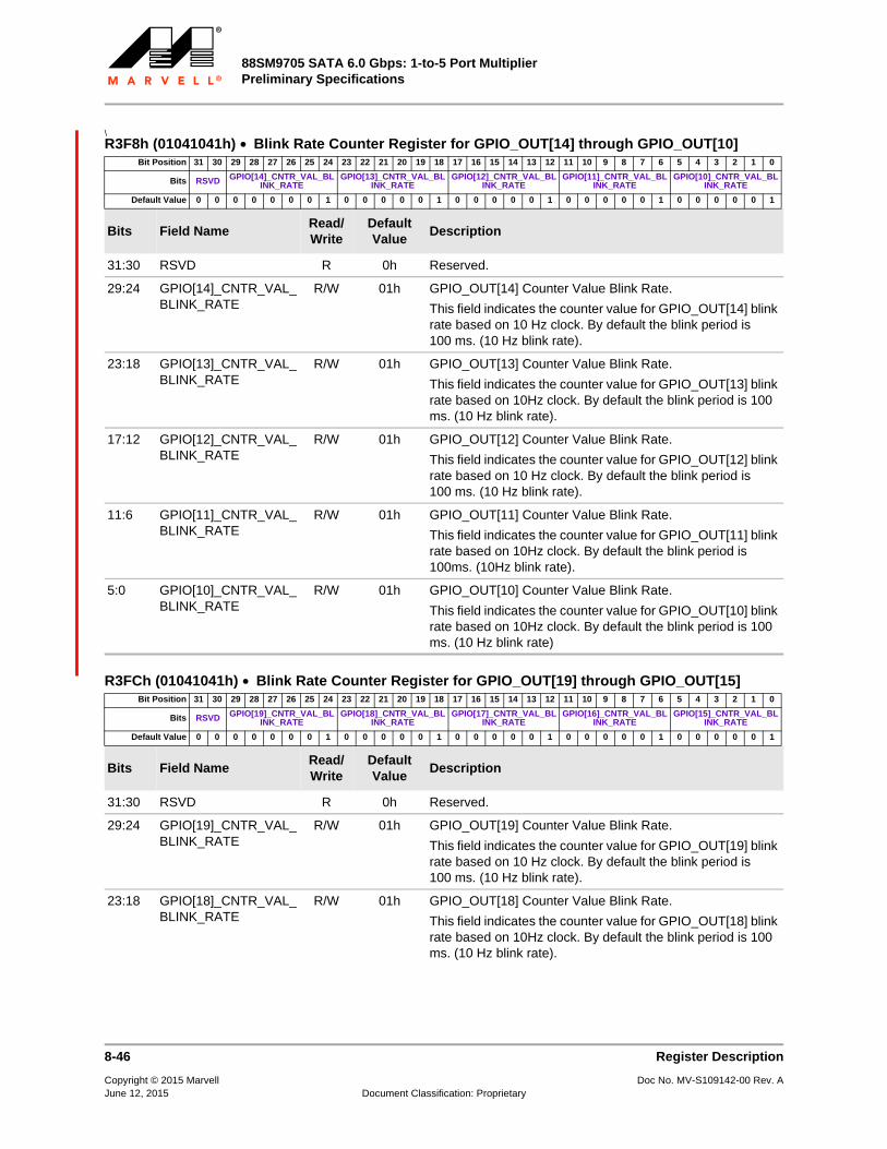
88SM9705 SATA 6.0 Gbps: 1-to-5 Port MultiplierPreliminary Specifications
\
R3F8h (01041041h) • Blink Rate Counter Register for GPIO_OUT[14] through GPIO_OUT[10] Bit Position 31 30 29 28 27 26 25 24 23 22 21 20 19 18 17 16 15 14 13 12 11 10 9 8 7 6 5 4 3 2 1 0
Bits RSVD GPIO[14]_CNTR_VAL_BLINK_RATE
GPIO[13]_CNTR_VAL_BLINK_RATE
GPIO[12]_CNTR_VAL_BLINK_RATE
GPIO[11]_CNTR_VAL_BLINK_RATE
GPIO[10]_CNTR_VAL_BLINK_RATE
Default Value 0 0 0 0 0 0 0 1 0 0 0 0 0 1 0 0 0 0 0 1 0 0 0 0 0 1 0 0 0 0 0 1
Bits Field NameRead/Write
Default Value
Description
31:30 RSVD R 0h Reserved.
29:24 GPIO[14]_CNTR_VAL_BLINK_RATE
R/W 01h GPIO_OUT[14] Counter Value Blink Rate.
This field indicates the counter value for GPIO_OUT[14] blink rate based on 10 Hz clock. By default the blink period is 100 ms. (10 Hz blink rate).
23:18 GPIO[13]_CNTR_VAL_BLINK_RATE
R/W 01h GPIO_OUT[13] Counter Value Blink Rate.
This field indicates the counter value for GPIO_OUT[13] blink rate based on 10Hz clock. By default the blink period is 100 ms. (10 Hz blink rate).
17:12 GPIO[12]_CNTR_VAL_BLINK_RATE
R/W 01h GPIO_OUT[12] Counter Value Blink Rate.
This field indicates the counter value for GPIO_OUT[12] blink rate based on 10 Hz clock. By default the blink period is 100 ms. (10 Hz blink rate).
11:6 GPIO[11]_CNTR_VAL_BLINK_RATE
R/W 01h GPIO_OUT[11] Counter Value Blink Rate.
This field indicates the counter value for GPIO_OUT[11] blink rate based on 10Hz clock. By default the blink period is 100ms. (10Hz blink rate).
5:0 GPIO[10]_CNTR_VAL_BLINK_RATE
R/W 01h GPIO_OUT[10] Counter Value Blink Rate.
This field indicates the counter value for GPIO_OUT[10] blink rate based on 10Hz clock. By default the blink period is 100 ms. (10 Hz blink rate)
R3FCh (01041041h) • Blink Rate Counter Register for GPIO_OUT[19] through GPIO_OUT[15] Bit Position 31 30 29 28 27 26 25 24 23 22 21 20 19 18 17 16 15 14 13 12 11 10 9 8 7 6 5 4 3 2 1 0
Bits RSVD GPIO[19]_CNTR_VAL_BLINK_RATE
GPIO[18]_CNTR_VAL_BLINK_RATE
GPIO[17]_CNTR_VAL_BLINK_RATE
GPIO[16]_CNTR_VAL_BLINK_RATE
GPIO[15]_CNTR_VAL_BLINK_RATE
Default Value 0 0 0 0 0 0 0 1 0 0 0 0 0 1 0 0 0 0 0 1 0 0 0 0 0 1 0 0 0 0 0 1
Bits Field NameRead/Write
Default Value
Description
31:30 RSVD R 0h Reserved.
29:24 GPIO[19]_CNTR_VAL_BLINK_RATE
R/W 01h GPIO_OUT[19] Counter Value Blink Rate.
This field indicates the counter value for GPIO_OUT[19] blink rate based on 10 Hz clock. By default the blink period is 100 ms. (10 Hz blink rate).
23:18 GPIO[18]_CNTR_VAL_BLINK_RATE
R/W 01h GPIO_OUT[18] Counter Value Blink Rate.
This field indicates the counter value for GPIO_OUT[18] blink rate based on 10Hz clock. By default the blink period is 100 ms. (10 Hz blink rate).
8-46 Register Description
Copyright © 2015 Marvell Doc No. MV-S109142-00 Rev. AJune 12, 2015 Document Classification: Proprietary
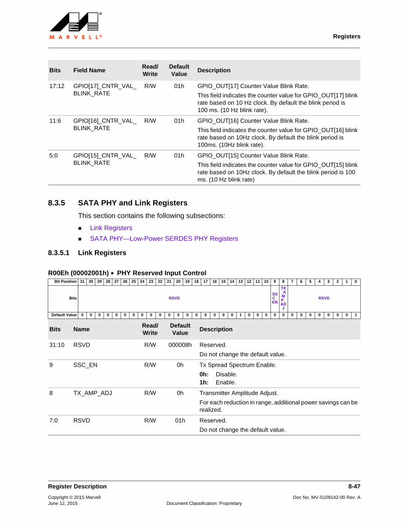
Registers
8.3.5 SATA PHY and Link Registers
This section contains the following subsections:
Link Registers
SATA PHY—Low-Power SERDES PHY Registers
8.3.5.1 Link Registers
17:12 GPIO[17]_CNTR_VAL_BLINK_RATE
R/W 01h GPIO_OUT[17] Counter Value Blink Rate.
This field indicates the counter value for GPIO_OUT[17] blink rate based on 10 Hz clock. By default the blink period is 100 ms. (10 Hz blink rate).
11:6 GPIO[16]_CNTR_VAL_BLINK_RATE
R/W 01h GPIO_OUT[16] Counter Value Blink Rate.
This field indicates the counter value for GPIO_OUT[16] blink rate based on 10Hz clock. By default the blink period is 100ms. (10Hz blink rate).
5:0 GPIO[15]_CNTR_VAL_BLINK_RATE
R/W 01h GPIO_OUT[15] Counter Value Blink Rate.
This field indicates the counter value for GPIO_OUT[15] blink rate based on 10Hz clock. By default the blink period is 100 ms. (10 Hz blink rate)
R00Eh (00002001h) • PHY Reserved Input ControlBit Position 31 30 29 28 27 26 25 24 23 22 21 20 19 18 17 16 15 14 13 12 11 10 9 8 7 6 5 4 3 2 1 0
Bits RSVDSSC_EN
TX_AMP_ADJ
RSVD
Default Value 0 0 0 0 0 0 0 0 0 0 0 0 0 0 0 0 0 0 1 0 0 0 0 0 0 0 0 0 0 0 0 1
Bits NameRead/Write
Default Value
Description
31:10 RSVD R/W 000008h Reserved.
Do not change the default value.
9 SSC_EN R/W 0h Tx Spread Spectrum Enable.
0h: Disable.1h: Enable.
8 TX_AMP_ADJ R/W 0h Transmitter Amplitude Adjust.
For each reduction in range, additional power savings can be realized.
7:0 RSVD R/W 01h Reserved.
Do not change the default value.
Bits Field NameRead/Write
Default Value
Description
Register Description 8-47
Copyright © 2015 Marvell Doc No. MV-S109142-00 Rev. AJune 12, 2015 Document Classification: Proprietary
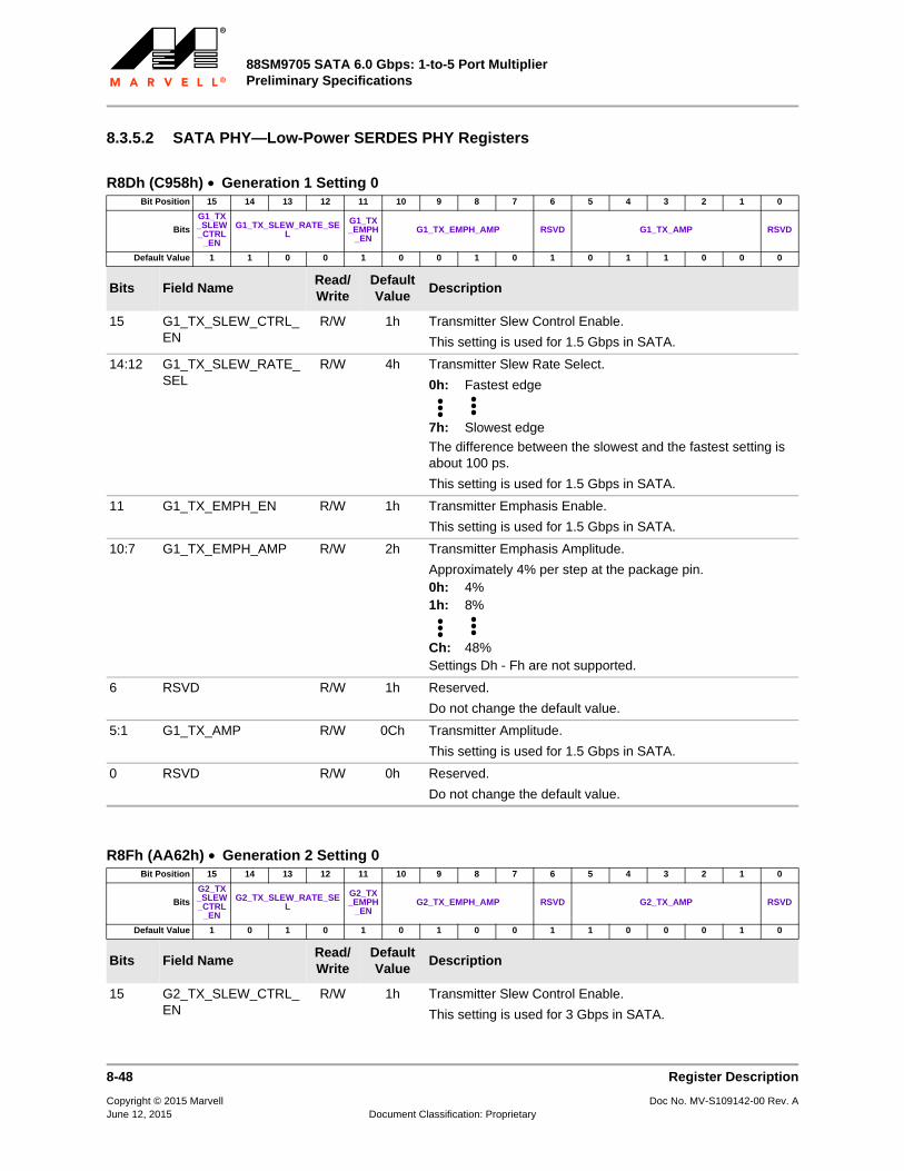
88SM9705 SATA 6.0 Gbps: 1-to-5 Port MultiplierPreliminary Specifications
8.3.5.2 SATA PHY—Low-Power SERDES PHY Registers
R8Dh (C958h) • Generation 1 Setting 0Bit Position 15 14 13 12 11 10 9 8 7 6 5 4 3 2 1 0
Bits
G1_TX_SLEW_CTRL
_EN
G1_TX_SLEW_RATE_SEL
G1_TX_EMPH
_ENG1_TX_EMPH_AMP RSVD G1_TX_AMP RSVD
Default Value 1 1 0 0 1 0 0 1 0 1 0 1 1 0 0 0
Bits Field NameRead/Write
Default Value
Description
15 G1_TX_SLEW_CTRL_EN
R/W 1h Transmitter Slew Control Enable.
This setting is used for 1.5 Gbps in SATA.
14:12 G1_TX_SLEW_RATE_SEL
R/W 4h Transmitter Slew Rate Select.
0h: Fastest edge
7h: Slowest edge
The difference between the slowest and the fastest setting is about 100 ps.
This setting is used for 1.5 Gbps in SATA.
11 G1_TX_EMPH_EN R/W 1h Transmitter Emphasis Enable.
This setting is used for 1.5 Gbps in SATA.
10:7 G1_TX_EMPH_AMP R/W 2h Transmitter Emphasis Amplitude.
Approximately 4% per step at the package pin.0h: 4%1h: 8%
Ch: 48%Settings Dh - Fh are not supported.
6 RSVD R/W 1h Reserved.
Do not change the default value.
5:1 G1_TX_AMP R/W 0Ch Transmitter Amplitude.
This setting is used for 1.5 Gbps in SATA.
0 RSVD R/W 0h Reserved.
Do not change the default value.
R8Fh (AA62h) • Generation 2 Setting 0Bit Position 15 14 13 12 11 10 9 8 7 6 5 4 3 2 1 0
Bits
G2_TX_SLEW_CTRL
_EN
G2_TX_SLEW_RATE_SEL
G2_TX_EMPH
_ENG2_TX_EMPH_AMP RSVD G2_TX_AMP RSVD
Default Value 1 0 1 0 1 0 1 0 0 1 1 0 0 0 1 0
Bits Field NameRead/Write
Default Value
Description
15 G2_TX_SLEW_CTRL_EN
R/W 1h Transmitter Slew Control Enable.
This setting is used for 3 Gbps in SATA.
8-48 Register Description
Copyright © 2015 Marvell Doc No. MV-S109142-00 Rev. AJune 12, 2015 Document Classification: Proprietary
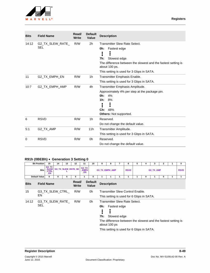
Registers
14:12 G2_TX_SLEW_RATE_SEL
R/W 2h Transmitter Slew Rate Select.
0h: Fastest edge
7h: Slowest edge
The difference between the slowest and the fastest setting is about 100 ps.
This setting is used for 3 Gbps in SATA.
11 G2_TX_EMPH_EN R/W 1h Transmitter Emphasis Enable.
This setting is used for 3 Gbps in SATA.
10:7 G2_TX_EMPH_AMP R/W 4h Transmitter Emphasis Amplitude.
Approximately 4% per step at the package pin.0h: 4%1h: 8%
Ch: 48%Others: Not supported.
6 RSVD R/W 1h Reserved.
Do not change the default value.
5:1 G2_TX_AMP R/W 11h Transmitter Amplitude.
This setting is used for 3 Gbps in SATA.
0 RSVD R/W 0h Reserved.
Do not change the default value.
R91h (0BEBh) • Generation 3 Setting 0Bit Position 15 14 13 12 11 10 9 8 7 6 5 4 3 2 1 0
Bits
G3_TX_SLEW_CTRL
_EN
G3_TX_SLEW_RATE_SEL
G3_TX_EMPH
_ENG3_TX_EMPH_AMP RSVD G3_TX_AMP RSVD
Default Value 0 0 0 0 1 0 1 1 1 1 1 0 1 0 1 1
Bits Field NameRead/Write
Default Value
Description
15 G3_TX_SLEW_CTRL_EN
R/W 0h Transmitter Slew Control Enable.
This setting is used for 6 Gbps in SATA.
14:12 G3_TX_SLEW_RATE_SEL
R/W 0h Transmitter Slew Rate Select.
0h: Fastest edge
7h: Slowest edge
The difference between the slowest and the fastest setting is about 100 ps
This setting is used for 6 Gbps in SATA.
Bits Field NameRead/Write
Default Value
Description
Register Description 8-49
Copyright © 2015 Marvell Doc No. MV-S109142-00 Rev. AJune 12, 2015 Document Classification: Proprietary
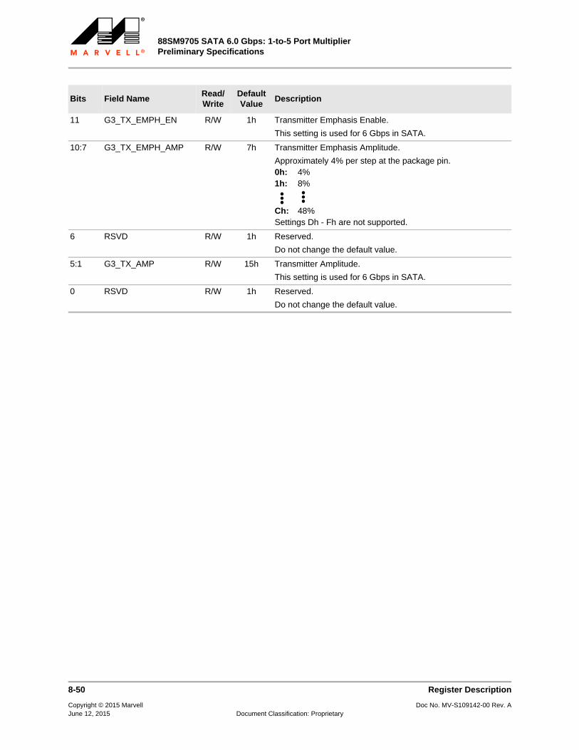
88SM9705 SATA 6.0 Gbps: 1-to-5 Port MultiplierPreliminary Specifications
11 G3_TX_EMPH_EN R/W 1h Transmitter Emphasis Enable.
This setting is used for 6 Gbps in SATA.
10:7 G3_TX_EMPH_AMP R/W 7h Transmitter Emphasis Amplitude.
Approximately 4% per step at the package pin.0h: 4%1h: 8%
Ch: 48%Settings Dh - Fh are not supported.
6 RSVD R/W 1h Reserved.
Do not change the default value.
5:1 G3_TX_AMP R/W 15h Transmitter Amplitude.
This setting is used for 6 Gbps in SATA.
0 RSVD R/W 1h Reserved.
Do not change the default value.
Bits Field NameRead/Write
Default Value
Description
8-50 Register Description
Copyright © 2015 Marvell Doc No. MV-S109142-00 Rev. AJune 12, 2015 Document Classification: Proprietary

Registers
8.3.6 Device Port PHY Event Counter Registers
R100h (00000000h) • Device Port PHY Event Counter 0 Bit Position 31 30 29 28 27 26 25 24 23 22 21 20 19 18 17 16 15 14 13 12 11 10 9 8 7 6 5 4 3 2 1 0
Bits DEV_PORT_PHY_EVENT_CNTR_0
Default Value 0 0 0 0 0 0 0 0 0 0 0 0 0 0 0 0 0 0 0 0 0 0 0 0 0 0 0 0 0 0 0 0
Bits Field NameRead/Write
Default Value
Description
31:0 DEV_PORT_PHY_EVENT_CNTR_0
R/W 00000000h Device Port PHY Event Counter 0.
This register contains both the identifier and the counter value.
Counter identifier: 00002C00h.
Counter: 32-bit counter, contains number of transmitted H2D non-data FISes to which the port multiplier responded with R_ERR due to collision.
R101h (00000000h) • Device Port PHY Event Counter 2 Bit Position 31 30 29 28 27 26 25 24 23 22 21 20 19 18 17 16 15 14 13 12 11 10 9 8 7 6 5 4 3 2 1 0
Bits DEV_PORT_PHY_EVENT_CNTR_2
Default Value 0 0 0 0 0 0 0 0 0 0 0 0 0 0 0 0 0 0 0 0 0 0 0 0 0 0 0 0 0 0 0 0
Bits Field NameRead/Write
Default Value
Description
31:0 DEV_PORT_PHY_EVENT_CNTR_2
R/W 00000000h Device Port PHY Event Counter 2.
This register contains both the identifier and the counter value.
Counter identifier: 00002C02h.
Counter: 32-bit counter, contains number of corrupted CRC values that were transmitted to the host.
Register Description 8-51
Copyright © 2015 Marvell Doc No. MV-S109142-00 Rev. AJune 12, 2015 Document Classification: Proprietary
88SM9705 SATA 6.0 Gbps: 1-to-5 Port MultiplierPreliminary Specifications
THIS PAGE LEFT INTENTIONALLY BLANK
8-52 Register Description
Copyright © 2015 Marvell Doc No. MV-S109142-00 Rev. AJune 12, 2015 Document Classification: Proprietary
Electrical Specifications
9 ELECTRICAL SPECIFICATIONS
This chapter contains the following sections:
Absolute Maximum Ratings
Power Requirements
Recommended/Typical Operating Conditions
DC Characteristics
Thermal Data
9-1
Copyright © 2015 Marvell Doc No. MV-S109142-00 Rev. AJune 12, 2015 Document Classification: Proprietary
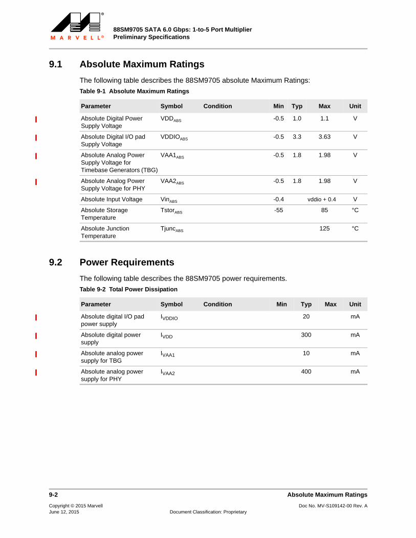
88SM9705 SATA 6.0 Gbps: 1-to-5 Port MultiplierPreliminary Specifications
9.1 Absolute Maximum Ratings
The following table describes the 88SM9705 absolute Maximum Ratings:
9.2 Power Requirements
The following table describes the 88SM9705 power requirements.
Table 9-1 Absolute Maximum Ratings
Parameter Symbol Condition Min Typ Max Unit
Absolute Digital Power Supply Voltage
VDDABS -0.5 1.0 1.1 V
Absolute Digital I/O pad Supply Voltage
VDDIOABS -0.5 3.3 3.63 V
Absolute Analog Power Supply Voltage for Timebase Generators (TBG)
VAA1ABS -0.5 1.8 1.98 V
Absolute Analog Power Supply Voltage for PHY
VAA2ABS -0.5 1.8 1.98 V
Absolute Input Voltage VinABS -0.4 vddio + 0.4 V
Absolute Storage Temperature
TstorABS -55 85 °C
Absolute Junction Temperature
TjuncABS 125 °C
Table 9-2 Total Power Dissipation
Parameter Symbol Condition Min Typ Max Unit
Absolute digital I/O pad power supply
IVDDIO 20 mA
Absolute digital power supply
IVDD 300 mA
Absolute analog power supply for TBG
IVAA1 10 mA
Absolute analog power supply for PHY
IVAA2 400 mA
9-2 Absolute Maximum Ratings
Copyright © 2015 Marvell Doc No. MV-S109142-00 Rev. AJune 12, 2015 Document Classification: Proprietary
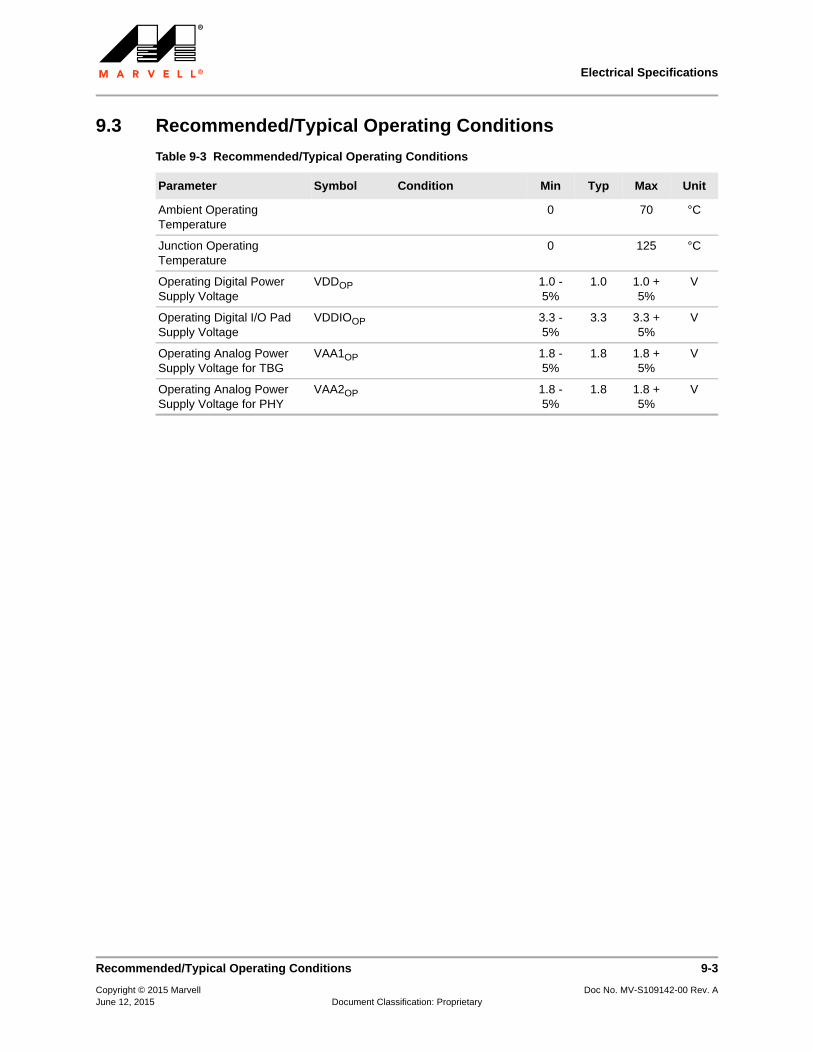
Electrical Specifications
9.3 Recommended/Typical Operating Conditions
Table 9-3 Recommended/Typical Operating Conditions
Parameter Symbol Condition Min Typ Max Unit
Ambient Operating Temperature
0 70 °C
Junction Operating Temperature
0 125 °C
Operating Digital Power Supply Voltage
VDDOP 1.0 - 5%
1.0 1.0 + 5%
V
Operating Digital I/O Pad Supply Voltage
VDDIOOP 3.3 - 5%
3.3 3.3 + 5%
V
Operating Analog Power Supply Voltage for TBG
VAA1OP 1.8 - 5%
1.8 1.8 + 5%
V
Operating Analog Power Supply Voltage for PHY
VAA2OP 1.8 - 5%
1.8 1.8 + 5%
V
Recommended/Typical Operating Conditions 9-3
Copyright © 2015 Marvell Doc No. MV-S109142-00 Rev. AJune 12, 2015 Document Classification: Proprietary

88SM9705 SATA 6.0 Gbps: 1-to-5 Port MultiplierPreliminary Specifications
9.4 DC Characteristics
Table 9-4 DC Characteristics
Parameter Symbol Condition Min Typ Max Unit
Input Low Voltage VIL -0.4 0.8 V
Input High Voltage VIH 2.0 VDDIO + 0.4 V
Output Low Voltage VOL IOL=4 mA, VDDP=3.3V -0.4 0.13 0.4 V
Output High Voltage VOH IOL=-2 mA, VDDP=3.3V 2.4 3.3 V
9-4 DC Characteristics
Copyright © 2015 Marvell Doc No. MV-S109142-00 Rev. AJune 12, 2015 Document Classification: Proprietary
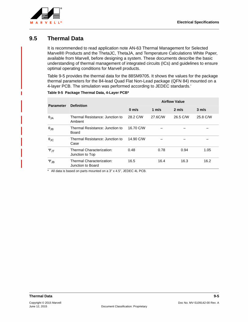
Electrical Specifications
9.5 Thermal Data
It is recommended to read application note AN-63 Thermal Management for Selected Marvell® Products and the ThetaJC, ThetaJA, and Temperature Calculations White Paper, available from Marvell, before designing a system. These documents describe the basic understanding of thermal management of integrated circuits (ICs) and guidelines to ensure optimal operating conditions for Marvell products.
Table 9-5 provides the thermal data for the 88SM9705. It shows the values for the package thermal parameters for the 84-lead Quad Flat Non-Lead package (QFN 84) mounted on a 4-layer PCB. The simulation was performed according to JEDEC standards.‘
Table 9-5 Package Thermal Data, 4-Layer PCB*
* All data is based on parts mounted on a 3” x 4.5”, JEDEC 4L PCB.
Parameter DefinitionAirflow Value
0 m/s 1 m/s 2 m/s 3 m/s
θJA Thermal Resistance: Junction to Ambient
28.2 C/W 27.6C/W 26.5 C/W 25.8 C/W
θJB Thermal Resistance: Junction to Board
16.70 C/W – – –
θJC Thermal Resistance: Junction to Case
14.90 C/W – – –
ΨJT Thermal Characterization: Junction to Top
0.48 0.78 0.94 1.05
ΨJB Thermal Characterization: Junction to Board
16.5 16.4 16.3 16.2
Thermal Data 9-5
Copyright © 2015 Marvell Doc No. MV-S109142-00 Rev. AJune 12, 2015 Document Classification: Proprietary

88SM9705 SATA 6.0 Gbps: 1-to-5 Port MultiplierPreliminary Specifications
THIS PAGE LEFT INTENTIONALLY BLANK
9-6 Thermal Data
Copyright © 2015 Marvell Doc No. MV-S109142-00 Rev. AJune 12, 2015 Document Classification: Proprietary