making better transistors: beyond yet another new
TRANSCRIPT

Making better transistors:
beyond yet another new materials system
Mark Rodwell, University of California, Santa Barbara
Dagstul Worshop, Feb 6-11, 2017.

What does VLSI need ?
Small transistors: plentiful, cheap
Small transistors→ short wiressmall delay CVDD /Ilow switching energy CVDD
2/2
Low supply voltageslow energy CVDD
2/2
Large on-currentssmall delay CVDD /I
0 0.1 0.2 0.3 0.4 0.510
-1
100
101
102
103
Vgs
60mV/decade
0 0.1 0.2 0.3 0.4 0.50
200
400
600
800
1000
Vgs
I d, A
mp
s/m
ete
r
Low leakage currentthermal: Ioff > Ion*exp(-qVDD/kT)want low VDD yet low Ioff.
Ion

Transistor Research
Make the switch smaller (scaling)
Make it from different materials
Change its shape
Change its internal operation:
bandgap engineering
Change what we do with it.

We can't make MOSFETs much smaller
Tunneling: can't make gate insulator any thinner
→ smaller devices have poor electrostatic control, don't turn off
Tunneling: can't make channel much shorter
→ smaller devices have high source-drain tunneling, don't turn off
Expensive lithography: EUV, multiple patterning

New Materials: III-V semiconductors ?
S. Lee et al., VLSI Symp. 2014
10 100
0.10
0.15
0.20
0.25
0.30
0.35
0.40
0.45
0.50
S. Lee, VLSI 2014
J. Lin, IEDM 2013
T. Kim, IEDM 2013
Intel, IEDM 2009
J. Gu, IEDM 2012
D. Kim, IEDM 2012
I on (
mA
/m
)
Gate Length (nm)
VDS
= 0.5 V
Ioff
=100 nA/m
Vertical Spacer
N+ S/D
Lg~25 nm
record for III-V
= best UTB SOI silicon

New Materials: 2-D semiconductors ?
0
0.05
0.1
0.15
0.2
0.25
0.3
0.35
0.01 0.1 1
no
rma
lized
drive
cu
rre
nt K
1
m*/mo
g=2isotropic
EET=1.0 nm
0.6 nm
0.4 nm
0
0.05
0.1
0.15
0.2
0.25
0.3
0.35
0.01 0.1 1
no
rma
lized
drive
cu
rre
nt,
K1
normalized effective mass m*/mo
EET=1.0 nm
0.6 nm0.4 nm g=6
isotropic
0
0.05
0.1
0.15
0.2
0.25
0.3
0.35
0.01 0.1 1
no
rma
lized
drive
cu
rre
nt,
K1
normalized longitudinal transport mass mL/m
o
EET=1.0 nm
0.6 nm0.4 nm
EET=Tox
SiO2/
ox+T
channel
SiO2/2
channel
g=1transverse mass
=2.6*mo
Silic
on
Mo
S 2P
ho
sph
ore
ne
2/32/1
||
2/1
,
2/12/1
2/3
)/()/(1
)/( where
, V 1m
mA84
oequivodos
o
thgs
mmmgcc
mmgK
VVKJ
Does 1-atom-thick channel help ?2D or 3D: the gate oxide won't scalethe oxide sets a minimum gate length1-atom-thick channels don't help much
If oxides won't scale, we must make finswith 2D, can we make fins ?later, will need to make nanowires...
Ballistic drive currents don't win eitherhigh m*, and/or high DOSmobility sufficient for ballistic ?
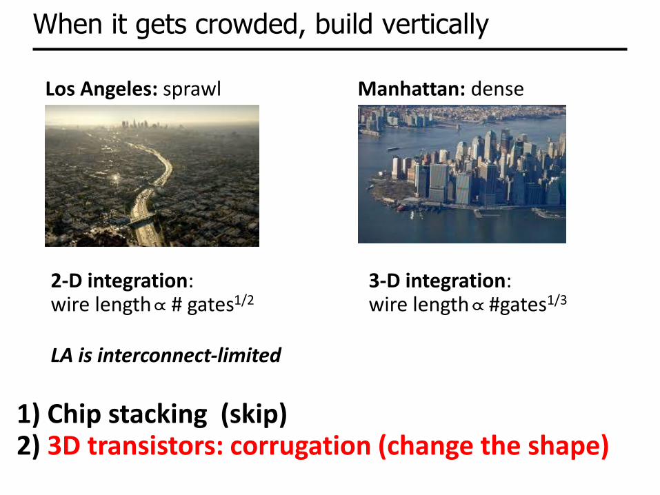
When it gets crowded, build vertically
2-D integration:wire length # gates1/2
Los Angeles: sprawl Manhattan: dense
3-D integration:wire length #gates1/3
LA is interconnect-limited
1) Chip stacking (skip)2) 3D transistors: corrugation (change the shape)

Corrugated surface→ more surface per die area

Corrugated surface→ more current per unit area
Cohen-Elias et al., UCSB2013 DRC
J .J. Gu et al., 2012 DRC,Purdue2012 IEDM

Corrugation: same current, less voltage, less CV2
0 0.1 0.2 0.3 0.4 0.5
10-1
100
101
102
103
Vgs
60mV/decade
I d,
Am
ps p
er
me
ter
of
FE
T f
oo
tprin
t w
idth
0 0.1 0.2 0.3 0.4 0.5
10-1
100
101
102
103
104
Vgs
I d,
Am
ps p
er
me
ter
of
FE
T f
ootp
rin
t w
idth
0 0.1 0.2 0.3 0.4 0.5
10-1
100
101
102
103
104
Vgs
10:1
corrugation
I d,
Am
ps p
er
me
ter
of
FE
T f
ootp
rin
t w
idth

Forming tall fins by sidewall regrowth (ugly)
Cohen-Elias et al., 2013 DRC

Confined Epitaxial Lateral Overgrowth
Semiconductor regrowth into hollow glass boxes formed on wafer surfaceSemiconductor thicknesses controlled by ALD layer thickness: atomic precision
L. Czornomaz et. al, (IBM)2015 & 2016 VLSI Symposia

CELO: Can we grow 3-D structures ?
With a few process tricks,can we make growth templates for 3-D structures ?

Fixing source-drain tunneling by increasing mass ?
Source-drain tunneling leakage:
)(*2 where),2exp( 1
thgoff qVmLI
2/1*constant gg LmL
0
0.05
0.1
0.15
0.2
0.25
0.3
0.35
0.01 0.1 1
no
rma
lized
drive
cu
rre
nt K
1
m*/mo
g=2
EET=1.0 nm
0.6 nm
0.4 nm
g=1
EET=Tox
SiO2/
ox+T
channel
SiO2/2
channel
Fix by increasing effective mass ?
This will decrease the on-current:
?
!
long gate→ big
shorter gate→ smaller
less current
wider→ more current
big again !
(also increases transit time)

Fixing source-drain tunneling by corrugation
Transport distance > gate footprint lengthOnly small capacitance increase
CY Huang et al, 2015 DRC

Fixing source-drain tunneling by corrugation ?
CELO growth over ridge
3D structure
transport length >> footprint
improves electrostatics...like finFET
improves S/D tunneling...unlike finFET
Gate oxide is SiOxNy , not HfO2 → thinner @ given leakageHow to reduce gate footprint below ~5nm ?

Changing the band structure: tunnel FETs
TFET: bandgap of p-type source truncates source thermal distribution:
-1.5
-1
-0.5
0
0.5
1
1.5
2
5 10 15 20 25
En
erg
y, eV
position, nm10
-310
-210
-110
0
-0.2
-0.1
0
0.1
0.2
0.3
0.4
0.5
Transmission
En
erg
y(e
V)
Problem: 4-6nm tunnel barriers→ ~3% tunneling probability→ very low current.

[110] gives more on-current than [100]
high confinement masslow transport mass
low confinement masshigh transport mass
P. Long et al., EDL 3/2016
valen
ce b
and

Add more Heterojunctions: much more current.
Added heterojunctions→ greater built-in potential→greater field→ thinner barrier→ higher tunneling probability (~80%)→ 30:1 more current.
-0.3
-0.2
-0.1
0
0.1
0.2
0.3
0 5 10 15 20
Ene
rgy, e
V
Position, nm
Efs
6 nmtunnelbarrier
-0.3
-0.2
-0.1
0
0.1
0.2
0.3
0 5 10 15 20
Ene
rgy, eV
Position, nmw
idegap
sourc
e
gra
de
wid
egap
channel
gra
de
GaS
b
InA
s
1.1nmtunnelbarrier
Source HJ: S. Brocard, et al., EDL, 2/2014; Channel HJ: P. Long et al., EDL 3/2016

3HJ still have higher ON/OFF ratio than GaAsSb/InAs
3HJ 516A/m
GaAsSb/InAs 75A/m
3HJ still have higher ON/OFF ratio than GaAsSb/InAs when acoustic and non-polar
optical phonon scattering are considered.
P. Long, J. Huang,
M. Povolotski: Purdue, Unpublished

Changing the function: ferroFETs ?
This won't work need tri-state driver
why not this ? or this ?
or an input switch.

Multiple Supplies for Low-Power Logic
-0.4 -0.2 0 0.2 0.4
Driver
10-1
100
101
102
103
Vgs
low
high
I on,
Am
ps/m
ete
r
-0.8 -0.6 -0.4 -0.2 0
Receiver
& Logic
Vgs
low
high
-0.8 -0.6 -0.4 -0.2 0
Logic
Vgs
low
high
Given 200 mV swingson long interconnects,
Line receivers provide0.1 mA/m outputwith 0.1 A/m leakage
Line drivers, and logic gates provide3 mA/m outputwith 0.1 A/m leakage
Is cost in added die area acceptable ?

(backup slides follow)

Record III-V MOS
S. Lee et al., VLSI 2014
10 100
0.10
0.15
0.20
0.25
0.30
0.35
0.40
0.45
0.50
S. Lee, VLSI 2014
J. Lin, IEDM 2013
T. Kim, IEDM 2013
Intel, IEDM 2009
J. Gu, IEDM 2012
D. Kim, IEDM 2012
I on (
mA
/m
)
Gate Length (nm)
VDS
= 0.5 V
Ioff
=100 nA/m
-0.3 -0.2 -0.1 0.0 0.1 0.2 0.3 0.4 0.510
-7
10-6
10-5
10-4
10-3
10-2
10-1
100
101
gm (
mS
/m
)
Cu
rren
t D
en
sit
y (
mA
/m
)
Gate Bias (V)
0.0
0.5
1.0
1.5
2.0
2.5
3.0L
g = 25 nm
SS~ 72 mV/dec.
SS~ 77 mV/dec.
Ion= 500 A/m at Ioff
=100 nA/m
and VD=0.5V
Vertical Spacer
N+ S/D
Lg~25 nm
recordfor III-V
= best UTB SOI silicon

Vertical FETs ????
Can have a smaller footprint.
No clue how to make it !
III-V nanowire growth: much too big

3D→shorter wires→less capacitance→less CV2
All three have same drive current, same gate width
Tall fin, "4-D": smaller footprint→ shorter wires

Minimum Dielectric Thickness & Gate Leakage
-6
-5.5
-5
-4.5
-4
-3.5
-3
-2.5
-2
eV
fro
m v
acu
um
leve
l
Si
InGaAs HfO2
TiO2
Ec
Ev
r ~20
r ~40
barrier
1
barrier *2 where),2exp(y Probabiliton Transmissi EmTP
→ 0.5-0.7nm minimum EOTconstrains on-currentelectrostatics degrades with scaling→ fins, nanowires
High-r materials have lower barriers
0
0.05
0.1
0.15
0.2
0.25
0.3
0.35
0.01 0.1 1
no
rma
lized
drive
cu
rre
nt K
1
m*/mo
g=2
EET=1.0 nm
0.6 nm
0.4 nm
g=1
EET=Tox
SiO2/
ox+T
channel
SiO2/2
channel
Thin dielectrics are leaky

Quick check: scaling limits
finFET: 5 nm physical gate length.Channel: <100> Si, 0.5, 1, or 2nm thick dielectric: r=12.7, 0.5 or 0.7 nm EOT
60
65
70
75
80
0 0.5 1 1.5 2 2.5
Dielectric: 0.5 nm EOT
su
bth
resh
old
sw
ing
, m
V/d
eca
de
body thickness, nm
thermionic+
tunneling
thermionic
only
5nm gate length
<100> Si finFET
0 0.5 1 1.5 2 2.5
Dielectric: 0.7nm EOT
body thickness, nm
thermionic+
tunneling
thermionic
only
NEMO ballistic simulations
Given EOT limits, ~1.5-2nm body is acceptable.
Source-drain tunneling often dominates leakage.
simulation
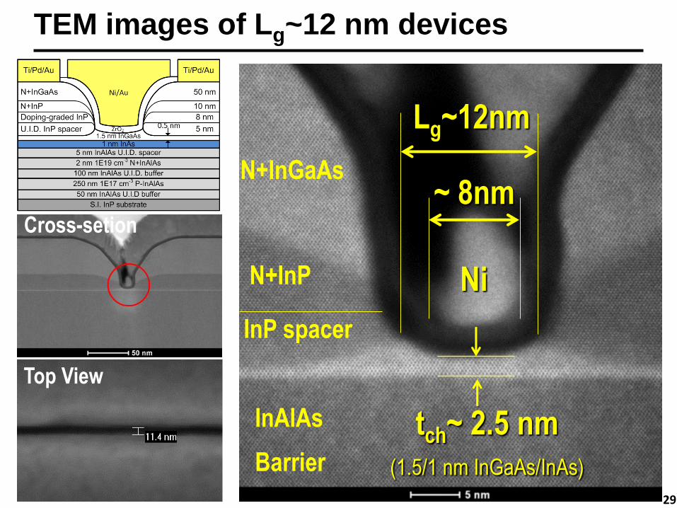
TEM images of Lg~12 nm devices
N+InGaAs
InP spacer
InAlAs
Barrier
Lg~12nm
~ 8nm
29
tch~ 2.5 nm
(1.5/1 nm InGaAs/InAs)
Top View
Ni
Cross-setion
N+InP

ID-VG and ID-VD curves of 12nm Lg FETs
30
0.0 0.2 0.4 0.6 0.80.0
0.2
0.4
0.6
0.8
1.0
gm (m
S/
m)I D
(m
A/
m)
VGS
(V)
0.0
0.4
0.8
1.2
1.6
2.0
2.4V
DS = 0.1 to 0.7 V,
0.2 V increment
0.0 0.1 0.2 0.3 0.4 0.5 0.6 0.70.0
0.5
1.0
1.5
I D (
mA
/m
)
VDS
(V)
Ron
= 302 Ohm-m
at VGS
= 1.0 V
VGS
= -0.2 V to 1.2 V
0.2 V increment
-0.2 0.0 0.2 0.4 0.6 0.810
-8
10-7
10-6
10-5
10-4
10-3
10-2
10-1
100
101
SS ~ 107.5 mV
at VDS
=0.5 V
SS ~ 98.6 mV
at VDS
=0.1 V
VDS
= 0.1 to 0.7 V
0.2 V increment
I D,
|IG| (m
A/
m)
VGS
(V)
Ioff~1.3 nA/μm Ion~1.1 mA/μm
Ion/Ioff > 8.3∙105
Lg-12nm
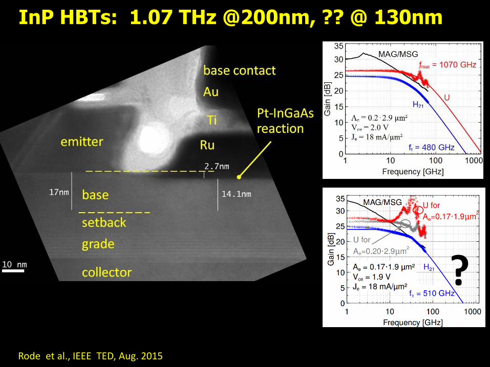
InP HBTs: 1.07 THz @200nm, ?? @ 130nm
?
Rode et al., IEEE TED, Aug. 2015

130nm /1.1 THz InP HBT: ICs to 670 GHz614 GHz fundamentalVCO
340 GHz dynamic frequency divider
Vout
VEE VBB
Vtune
Vout
VEE VBB
Vtune
620 GHz, 20 dB gain amplifierM Seo, TSCIMS 2013
also: 670GHz amplifierJ. Hacker , TSCIMS 2013 (not shown)
M. Seo, TSC / UCSB
M. Seo, UCSB/TSCIMS 2010
204 GHz static frequency divider(ECL master-slave latch)
Z. Griffith, TSCCSIC 2010
300 GHz fundamentalPLLM. Seo, TSCIMS 2011
220 GHz 180 mWpower amplifier T. Reed, UCSBCSICS 2013
600 GHz IntegratedTransmitterPLL + MixerM. Seo TSC
Integrated 300/350GHz Receivers:LNA/Mixer/VCO
M. Seo TSC
81 GHz 470 mWpower amplifier H-C Park UCSBIMS 2014