maharashtra state board of technical education...
TRANSCRIPT

MAHARASHTRA STATE BOARD OF TECHNICAL EDUCATION (Autonomous)
(ISO/IEC - 27001 - 2005 Certified) _____________________________________________________________________________________________
1
Winter – 15 EXAMINATIONS
Subject Code: 17443 Model Answer
Important Instructions to examiners:
1) The answers should be examined by key words and not as word-to-word as given in the answer scheme.
2) The model answer and the answer written by candidate may vary but the examiner may try to assess the understanding level of the candidate.
3) The language errors such as grammatical, spelling errors should not be given more Importance (Not applicable for subject English and Communication Skills.
4) While assessing figures, examiner may give credit for principal components indicated in the figure. The figures drawn by candidate and model answer may vary. The examiner may give credit for any equivalent figure drawn.
5) Credits may be given step wise for numerical problems. In some cases, the assumed constant values may vary and there may be some difference in the candidate’s answers and model answer.
6) In case of some questions credit may be given by judgment on part of examiner of relevant answer based on candidate’s understanding.
7) For programming language papers, credit may be given to any other program based on equivalent concept.

MAHARASHTRA STATE BOARD OF TECHNICAL EDUCATION (Autonomous)
(ISO/IEC - 27001 - 2005 Certified) _____________________________________________________________________________________________
2
1. a) Attempt any SIX of the following: (Marks 12)
i) What is accumulator? State its function.
Ans. (def.: 1 mark, function: 1 mark)
It is a 8 bit general purpose register connected to internal data bus and to ALU . It is used to
hold one of the operands of an arithmetic or logical operations. It serve one i/p to the
ALU. The final result of an arithmetic or logical operation is placed in the accumulator. It
is used in most of the arithmetic and logical instructions. The result of any operation
performed by ALU is stored in the accumulator.
ii) List the features of 8085.
Ans. (Any 4 features: 2 marks, ½ mark each feature)
It has 8 bit data bus, 8bit ALU. So it is 8 bit microprocessor.
has 16 bit address bus.
DMA feature using HOLD & HLDA Pins.
iii) Give two examples of direct addressing mode.
Ans. (Each example: 1 mark)
Examples-
LDA 2050H ;load A with contents of memory location with address 2050H
STA 3050H ;store A with contents of memory location with address 3050H
iv) Define register addressing mode.
Ans. (Define: 2 marks)
The register addressing mode specifies the source operand, or both to be contained in 8085
registers. This results in faster execution, since it is not necessary to access memory
locations for operands.
Example :MOV A,B
v) List the 8085 interrupt according to priority.
Ans. (List: 1 mark, priority: 1 mark)

MAHARASHTRA STATE BOARD OF TECHNICAL EDUCATION (Autonomous)
(ISO/IEC - 27001 - 2005 Certified) _____________________________________________________________________________________________
3
Interrupt
Priority
TRAP 1st
RST 7.5 2nd
RST 6.5 3rd
RST 5.5 4th
INTR 5th
vi) State the capacity of memory available in 8155.
Ans. (Correct answer: 2 marks)
It has 256 bytes of read write memory available.
vii) Write the function of any two pins of 8155.
Ans. (Function of each pin: 1 mark)
I/O memory select (IO/M): this pin selects either of the five register (Control,status,PA0-
PA7,PB0- PB7,PC0-PC5) or the memory portion.
ALE: It is used to latch the lower 8 bit address A7-A0 in the internal latch of 8155.
Read (RD/): when this pin is low the CPU can read the data from ports, registers and
memory.
Write (WR/): When this pin is low, the CPU can write data into ports, registers and
memory.
RESET: When this pin is high the control cleared, all the ports are set to simple input
mode and timer is stopped.
Chip Enable (CE/): this is active low input which must be enabled for the data transfer
operation.
/
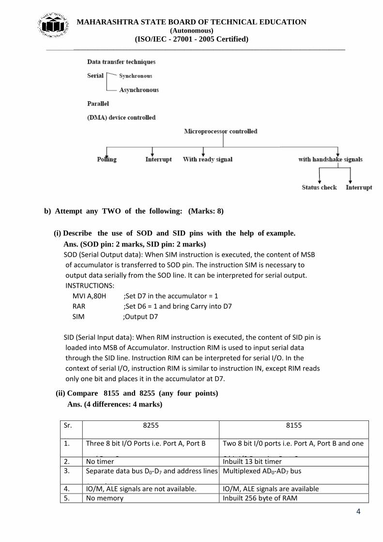
viii) Classify the data transfer techniques.
Ans. (Classification: 2 marks)
MAHARASHTRA STATE BOARD OF TECHNICAL EDUCATION (Autonomous)
(ISO/IEC - 27001 - 2005 Certified) _____________________________________________________________________________________________
4
b) Attempt any TWO of the following: (Marks: 8)
(i) Describe the use of SOD and SID pins with the help of example.
Ans. (SOD pin: 2 marks, SID pin: 2 marks)
SOD (Serial Output data): When SIM instruction is executed, the content of MSB
of accumulator is transferred to SOD pin. The instruction SIM is necessary to
output data serially from the SOD line. It can be interpreted for serial output.
INSTRUCTIONS:
MVI A,80H ;Set D7 in the accumulator = 1
RAR ;Set D6 = 1 and bring Carry into D7
SIM ;Output D7
SID (Serial Input data): When RIM instruction is executed, the content of SID pin is
loaded into MSB of Accumulator. Instruction RIM is used to input serial data
through the SID line. Instruction RIM can be interpreted for serial I/O. In the
context of serial I/O, instruction RIM is similar to instruction IN, except RIM reads
only one bit and places it in the accumulator at D7.
(ii) Compare 8155 and 8255 (any four points)
Ans. (4 differences: 4 marks)
Sr.
No.
8255 8155
1. Three 8 bit I/O Ports i.e. Port A, Port B
and Port C
Two 8 bit I/0 ports i.e. Port A, Port B and one
6 bit I/0 Ports i.e. Port C 2. No timer Inbuilt 13 bit timer 3. Separate data bus D0-D7 and address lines
A0 and A1
Multiplexed AD0-AD7 bus
4. IO/M, ALE signals are not available. IO/M, ALE signals are available 5. No memory Inbuilt 256 byte of RAM
MAHARASHTRA STATE BOARD OF TECHNICAL EDUCATION (Autonomous)
(ISO/IEC - 27001 - 2005 Certified) _____________________________________________________________________________________________
5
6. A0, A1 address lines are used to select I/O
ports, CWR.
A0, A1, A2 lines are used to select ports, CWR and timer register.
7. Port C is 8 bit can be used as two 4 bit
ports.
Port C is a 6 bit port
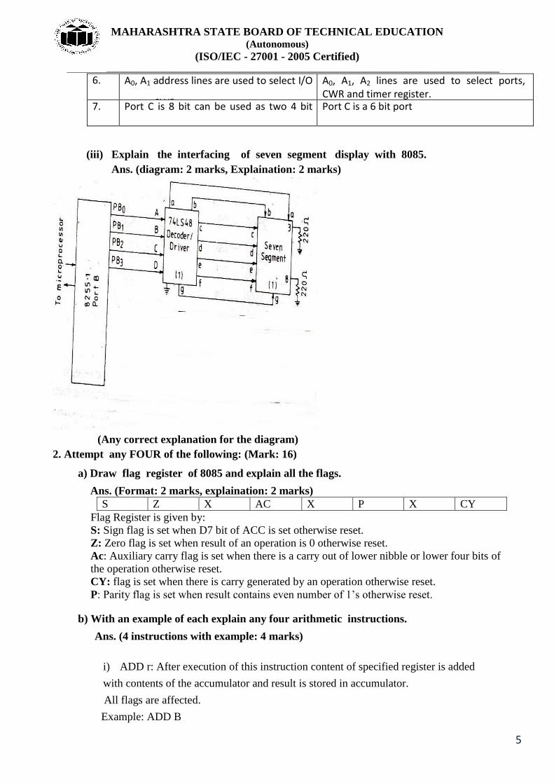
(iii) Explain the interfacing of seven segment display with 8085.
Ans. (diagram: 2 marks, Explaination: 2 marks)
(Any correct explanation for the diagram)
2. Attempt any FOUR of the following: (Mark: 16)
a) Draw flag register of 8085 and explain all the flags.
Ans. (Format: 2 marks, explaination: 2 marks)
S Z X AC X P X CY
Flag Register is given by:
S: Sign flag is set when D7 bit of ACC is set otherwise reset.
Z: Zero flag is set when result of an operation is 0 otherwise reset.
Ac: Auxiliary carry flag is set when there is a carry out of lower nibble or lower four bits of
the operation otherwise reset.
CY: flag is set when there is carry generated by an operation otherwise reset.
P: Parity flag is set when result contains even number of 1’s otherwise reset.
b) With an example of each explain any four arithmetic instructions.
Ans. (4 instructions with example: 4 marks)
i) ADD r: After execution of this instruction content of specified register is added
with contents of the accumulator and result is stored in accumulator.
All flags are affected.
Example: ADD B

MAHARASHTRA STATE BOARD OF TECHNICAL EDUCATION (Autonomous)
(ISO/IEC - 27001 - 2005 Certified) _____________________________________________________________________________________________
6
ii) ADI data: It is a two byte instruction .The data is added with content of the
accumulator .All flags are affected.
Example: ADI 56H
ii) SUB r: After execution of this instruction content of specified register is
subtracted from content of accumulator and the result is stored in accumulator.
All flags are affected.
Example SUB B
iii) SUI data: It is a two byte instruction .The data is subtracted from content of the
accumulator .All flags are affected.
Example: SUI 67H
c) Draw timing diagram of MOV A, B instruction.
Ans. (Correct timing diagram: 4 marks)
d) Describe the format of RIM and SIM instruction.
Ans. (RIM: 2 marks, SIM 2 marks)
Instruction RIM is Read Interrupt Mask.

MAHARASHTRA STATE BOARD OF TECHNICAL EDUCATION (Autonomous)
(ISO/IEC - 27001 - 2005 Certified) _____________________________________________________________________________________________
7
This is a 1-byte instruction that can be used to read interrupt masks.
This instruction loads the accumulator with 8 bits indicating the current status of the interrupt masks
To identify the pending interrupts bits D4, D5 and D6 are used.
To receive serial data bit D7 is used.
SOD – Serial Output Data: Bit D7 of the accumulator is latched into the SOD output line and
made available to a serial peripheral if bit D6=1;
SDE- Serial Data Enable: If this bit=1, it enables the serial output. To implement serial
output, this bit needs to be enabled.
XXX- Don’t care
R7.5-Reset RST 7.5 if this bit=1, RST 7.5 flip-Flop is reset. This is an additional control to
reset RST 7.5.
MSE- Mask Set Enable: if this bit is high, it enables the functions of bits D2, D1, D0. This id
master control over all the interrupt masking bits. If this bit is low, bits D2, D1 and D0 do not
have any effect on the masks.
M7.5-D2=0, RST 7.5 is enabled
=1, 7.5 is masked or disabled
M6.5-D1=0, RST 6.5 is enabled
=1, 6.5 is masked or disabled
M5.5-D0=0, RST 5.5 is enabled
=1, 5.5 is masked or disabled
e) Describe the memory mapped I/0 technique of interfacing.
Ans. (Correct explanation: 4 marks)
In this technique I/O and memory both are treated as Memory.
In this case both I/O and memory have a 16 bit address.
All memory related instructions are applicable for I/O devices and memory.
Size of memory is reduced
Arithmetic and logical operations can be directly performed on the I/O ports
Can interface maximum memory of 64 KB which also includes the I/O ports.
The data transfer is possible between any register and I/O port
f) Draw the block diagram of 8355.
Ans. (Correct diagram: 4 marks)

MAHARASHTRA STATE BOARD OF TECHNICAL EDUCATION (Autonomous)
(ISO/IEC - 27001 - 2005 Certified) _____________________________________________________________________________________________
8
Q3) Attempt any four of the following. (Marks: 16)
a) With the help of diagram explain the demultipexing of AD0 to AD7 bus.
Ans. (Diagram: 2 marks, Explanation: 2 marks)
Figure shows a schematic that uses a latch and the ALE signal to de multiplex the bus. The bus
AD7 –AD0 is connected as the input to the latch 74LS373.
MAHARASHTRA STATE BOARD OF TECHNICAL EDUCATION (Autonomous)
(ISO/IEC - 27001 - 2005 Certified) _____________________________________________________________________________________________
9
The ALE signal is connected to the Enable (G) pin of the latch, and the output control
(OC) signal of the latch is grounded.
The ALE goes high during T1. When the ALE is high, the latch is transparent; this means
that the output changes according to input data.
When the ALE goes low, the data byte is latched until the next ALE, and the output of the
latch represents the low-order address bus A7- A0 after the latching operation.
b) Explain any four addressing modes by giving an example of each.
Ans. (Any 4 addressing mode: 4 marks)
( any four addressing modes ,1 mark each.)
1) Immediate Addressing mode:-
In this mode of addressing the 8 bit or 16 bit operand (data) is a part of instruction .
MVI A,20H
2) Register Addressing mode:-
In this mode of addressing the operand (data) is in one of the general purpose register or
accumulator.
MOV B, A
3) Direct Addressing mode:-
In this mode of addressing the address of operand (data) is a part of instruction.
LDA 6020H
4) Indirect Addressing mode:-
In this mode of addressing the address of the operand (data) is specified by a register pair.
MOV B, M .
5) Implicit / Implied Addressing mode:-
In this mode of addressing the operand (data) is in accumulator.
RAR
Note: any valid example can be considered.
c) Write an assembly language program to multiply two eight bit numbers.
Ans. (Flowchart: 1 mark, Program with comments: 3 marks)
Flow chart:

MAHARASHTRA STATE BOARD OF TECHNICAL EDUCATION (Autonomous)
(ISO/IEC - 27001 - 2005 Certified) _____________________________________________________________________________________________
10
Label Program Comments
LDA 2200H ;Load contents of 2200H in accumulator
MOV E,A
MVI D,00 ;Get the first number in DE register pair
LDA 2201H
MOV C,A ;Initialize counter
LXI H,0000H ;Result=0
BACK: DAD D ;Result=Result+first number
DCR C ;Decrement count
JNZ BACK ;If count is not equal to zero, repeat
SHLD 2300H ;Store result
HLT ;Terminate program execution
d) Write a time delay subroutine using 8 bit register. Calculate the delay generated.
Assume suitable count in register.

MAHARASHTRA STATE BOARD OF TECHNICAL EDUCATION (Autonomous)
(ISO/IEC - 27001 - 2005 Certified) _____________________________________________________________________________________________
11
Ans. (Delay subroutine -2marks,calculation of delay-2marks)
Subroutine for time delay
Number of T states
MVI C,count ;Load count 7 T states
BACK : DCR C ;Decrement count 4 T states
JNZ BACK ;If count is not equal
to zero repeat
10/7 T states
Total T state required to execute the given subroutine=7+(count-1)x(4+10)+(4+7)
Assume count=5
Assume operating frequency of 8085is 2MHz
So for count=5,Toatal number of T state will be=7+(5-1)x(4+10)+(4+7)=74
Time required for 1 T state=1/2MHz=0.5microsec.
Total delay=74x0.5microsec=37microsec.
e) Interface 8k ROM to 8085. State the memory map.
Ans. (Interface diagram: 2 marks, Memory map: 2 marks)

MAHARASHTRA STATE BOARD OF TECHNICAL EDUCATION (Autonomous)
(ISO/IEC - 27001 - 2005 Certified) _____________________________________________________________________________________________
12
A1
5
A1
4
A1
3
A1
2
A1
1
A1
0
A
9
A
8
A
7
A
6
A
5
A
4
A
3
A
2
A
1
A
0
Start
adress
1 0 0 0 0 0 0 0 0 0 0 0 0 0 0 0 8000H
End
addres
s
1 0 0 1 0 0 0 0 0 0 0 0 0 0 0 0 9FFF
H
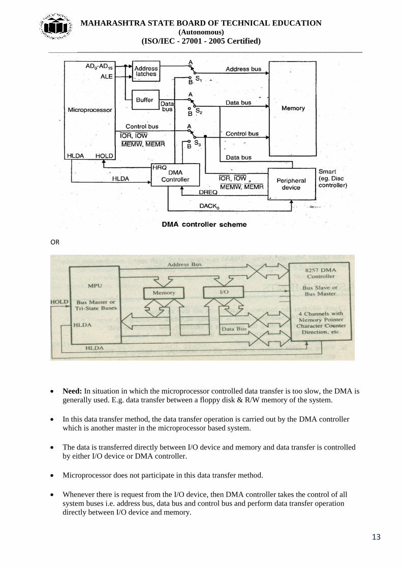
f) Describe the DMA controlled data transfer technique.
Ans. (Diagram: 1 mark, Explanation: 3 marks)
MAHARASHTRA STATE BOARD OF TECHNICAL EDUCATION (Autonomous)
(ISO/IEC - 27001 - 2005 Certified) _____________________________________________________________________________________________
13
OR
Need: In situation in which the microprocessor controlled data transfer is too slow, the DMA is generally used. E.g. data transfer between a floppy disk & R/W memory of the system.
In this data transfer method, the data transfer operation is carried out by the DMA controller which is another master in the microprocessor based system.
The data is transferred directly between I/O device and memory and data transfer is controlled by either I/O device or DMA controller.
Microprocessor does not participate in this data transfer method.
Whenever there is request from the I/O device, then DMA controller takes the control of all
system buses i.e. address bus, data bus and control bus and perform data transfer operation directly between I/O device and memory.

MAHARASHTRA STATE BOARD OF TECHNICAL EDUCATION (Autonomous)
(ISO/IEC - 27001 - 2005 Certified) _____________________________________________________________________________________________
14
This method is used when the large amount of data is required to be transfer.
IN IBM PC, Hard disk drive, floppy disk drive CD- ROM etc. devices uses this method of data
transfer.
In this method , when an I/O device wishes for data transfer, an I/O device itself generate
request signal DREQ to DMA controller.
In response to DREQ, the DMA controller send HOLD signal to the microprocessor.
After receiving HOLD signal, microprocessor performs current operation completely and
transfer the control of all system buses i.e. address bus, data bus and control bus to DMA
controller.
The DMA controller start data transfer operation.
The speed of the data transfer is faster as compare to programmed I/O data transfer method.
The three data transfer schemes of DMA are as given below:
Single Byte Transfer
Block Transfer
Hidden or Transparent DMA
Single Byte Transfer:
Only one byte data is Transferred at a time – data transfer speed is low.
In this mode of DMA data transfer, only one byte of data is transferred at a time, hence the data
transfer speed is slow.
DMA controller send HOLD signal to microprocessor and wait for HLDA (Acknowledge)
signal.
After receiving HLDA signal from microprocessor, the DMA enter into master mode and gain
the control of all system buses and execute only one DMA cycle to transfer one byte of data.
After transferring one byte of data, the DMA controller disable HOLD signal, enter into slave
mode and transfer the control of system buses to the microprocessor.
This process is repeated to transfer all data bytes. Means, the DMA controller enables and
disable HOLD signal for all data bytes transfer
Block Transfer:
In this mode of DMA data transfer, the block of data bytes is transferred continuously.
During the DMA data transfer, the microprocessor is disconnected from the system buses, hence
the microprocessor can not executes its own programs.
N number of DMA cycle are added into the machine cycle of the microprocessor where N
indicates numbers of bytes to be transferred.
In this mode, the DMA controller sends HOLD signal to the microprocessor to gain the control
of the system buses and wait for HLDA signal.
After receiving HLDA signal, the DMA controller enters into the master mode and starts data
transfer operation.
MAHARASHTRA STATE BOARD OF TECHNICAL EDUCATION (Autonomous)
(ISO/IEC - 27001 - 2005 Certified) _____________________________________________________________________________________________
15
After transferring all data bytes of the block, the DMA controller disable HOLD signal and enter
into the slave mode.
This mode DMA data transfer is faster than single byte mode.
Hidden or Transparent DMA:
In the machine cycle of microprocessor, there are some states during which all buses are not
used by the microprocessor means it floats system buses.
During these states, the microprocessor is isolated from the system buses and DMA controller
transfer data between I/O device and memory.
This is slowest DMA data transfer. In this method, additional logic i.e. hardware is required to
detect the idle states when the microprocessor floats its buses.
Q4. Attempt any four of the following (Marks: 16 marks)
a) Explain the following blocks of 8085:
i) ALU ii) Temporary register iii) Interrupt controller iv) Timing and control unit.
Explanation of 4 blocks: 01 Mark each
i) ALU: Arithmetic Logic unit: It performs arithmetic & logical operations like addition ,
subtraction, AND , OR , complement , rotate etc. on 8 bit data.
ii) Temporary registers W and Z: used internally by 8085 to hold 8 bit data temporarily during
execution of some instructions
iii) The processor fetches, decodes, and executes instructions in a sequence. Sometimes its
necessary for the microprocessor to execute a special routine for special condition. The most
impritant thing is after execution of special routine the program control must be transferred to the
program which processor was executing before the occurance of the special condition. It accepts
interrupt request. They are TRAP (highest priority) RST 7.5, RST 6.5, RST 5.5 and INTR (lowest
priority) and one acknowledge symbol /INTA. These interrupts have fixed priority.
iv) Timing and Control unit: Synchronizes all microprocessor operations with clock and
generates l signals necessary for instruction execution and communication between peripheral
devices & microprocessor
b) Explain LDA address and STA address instruction by giving two examples of each.
Ans. (Each instruction: 2 marks)
LDA addr: Load data into A register directly from the address given within the instruction.
This instruction copies the contents of the memory location whose address is given within the
instruction into the accumulator. The contents of the memory location remain unchanged.
Example1: LDA 2000H :This instruction will copy the contents of the memory location 2000H into the
Accumulator.
Before execution After execution
MAHARASHTRA STATE BOARD OF TECHNICAL EDUCATION (Autonomous)
(ISO/IEC - 27001 - 2005 Certified) _____________________________________________________________________________________________
16
A A 30H
2000H 30H 2000H 30H
Example2: LDA 1200H : This instruction will copy the contents of the memory location 1200H into the
Accumulator.
Before execution After execution
A A 40H
1200H 40H 1200H 40H
STA address: store the contents of A register at address given within the instruction
This instruction stores the contents of A register into the memory location whose address is directly
specified within the instruction .The contents of A register remain unchanged.
Example1: STA 2000H:This instruction will store the contents of A register (50H) to 2000H
Before execution After execution
A 50H A 50H
2000H 2000H 50H
Example2: STA 3000H:This instruction will store the contents of A register (80H) to 3000H
Before execution After execution
A 80H A 80H
3000H 3000H 80H
c) Write a program to add three 8 bit numbers available at memory location 1200H,1201H and
1202H.
Ans. (Flowchart: 1 mark, correct program with comments: 3 marks)
Flowchart:

MAHARASHTRA STATE BOARD OF TECHNICAL EDUCATION (Autonomous)
(ISO/IEC - 27001 - 2005 Certified) _____________________________________________________________________________________________
17
Program Comments
LXI H,1200H ;HL points to 1200H
MOV A,M ;Get first operand
INX H ;HL points to 1201H
ADD M ;Add second operand
INX H ;HL points to 1202H
ADD M ;Add third operand
HLT ;Terminate program execution
d) Describe the I/O mapped I/O interfacing technique.
Ans. (Correct explanation: 4 marks)
In this technique I/O is treated as I/O and memory is treated as Memory
In this case I/O has an 8 bit address and memory has a 16 bit address.
IN and OUT instructions are used for I/O devices and memory related instructions for memory.
Size of Memory is not reduced.
Arithmetic and logical operations cannot be directly performed on the I/O ports
Can interface maximum memory of 64 KB and 256 I/O ports.
The data transfer is possible only between Acc and I/O port.
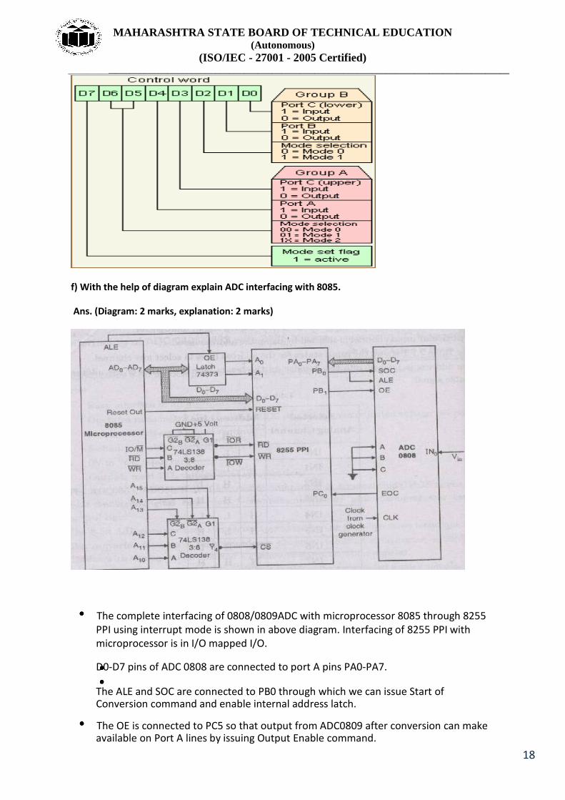
e) Explain the control word format of 8255.
Ans. (Correct control word format: 4 marks)
MAHARASHTRA STATE BOARD OF TECHNICAL EDUCATION (Autonomous)
(ISO/IEC - 27001 - 2005 Certified) _____________________________________________________________________________________________
18
f) With the help of diagram explain ADC interfacing with 8085.
Ans. (Diagram: 2 marks, explanation: 2 marks)
The complete interfacing of 0808/0809ADC with microprocessor 8085 through 8255 PPI using interrupt mode is shown in above diagram. Interfacing of 8255 PPI with microprocessor is in I/O mapped I/O.
D0-D7 pins of ADC 0808 are connected to port A pins PA0-PA7.
The ALE and SOC are connected to PB0 through which we can issue Start of Conversion command and enable internal address latch.
The OE is connected to PC5 so that output from ADC0809 after conversion can make available on Port A lines by issuing Output Enable command.

MAHARASHTRA STATE BOARD OF TECHNICAL EDUCATION (Autonomous)
(ISO/IEC - 27001 - 2005 Certified) _____________________________________________________________________________________________
19
0 0 0 0 0 0 0 1
The end of conversion EOC signal can be read from port C; hence the EOC pin is
connected to
PC4 of the port C of 8255PPI.
The input selection pin A, B and C of ADC 0809 are grounded to select only IN0.
The PC3 pin of 8255 is connected to RST5.5 interrupt of 8085, so that 8085 can be interrupted to read data from ADC 0808.
When SOC and ALE signals are received by ADC0808 from 8085 through 8255 PPI, the
ADC
starts the conversion.
After the conversion ADC0808 generates the EOC signal which will be received by 8255
on
PC4 as a STROBE signal. After receiving EOC signal 8255 generates OE signal on PC5
and interrupt signal on PC3 which is connected to RST5.5 interrupt of 8085.
The 8085 receives interrupt signal on RST5.5 and executes ISR to read digital data from
port A
The control word to initialize 8255 is given when Port A is configured as an input, Port B as as an output, Port C lower as input in mode 1
Clock to the ADC 0808 is connected to external clock generating circuitry. The control
word is B9H
D7 D6 D5 D4 D3 D2 D1
D0
1 0 1 1 1 0 0 1 The start of conversion command is given in figure where D0 bit is 1 i.e PB0 =1 and then a D0 bit is 0 to get one high pulse to start conversion.
D7 D6 D5 D4 D3 D2 D1
D0
D7 D6 D5 D4 D3 D2 D1 D0
0 0 0 0 0 0 0 0
5. Attempt any FOUR of the following: 16

MAHARASHTRA STATE BOARD OF TECHNICAL EDUCATION (Autonomous)
(ISO/IEC - 27001 - 2005 Certified) _____________________________________________________________________________________________
20
a) Generate the various control signals using gates.
Ans: (2M-Diagram,2M-truth table)
The basic control signals are generated using IO/M with S1, S0 Status Signals as follows.
b) Write an assembly language program to find largest and smallest number from a data block of 8
numbers. All numbers are 8 bit.
Ans:
LXI H, VAR
MOV C , M ; COUNTER
INX H
DCR C
MOV B, M ; FOR LARGEST
MOV D, M ; FOR SMALLEST
MOV A, M
BACK: CMP B
JC AHEAD
MOV B, A
AHEAD: CMP D
MAHARASHTRA STATE BOARD OF TECHNICAL EDUCATION (Autonomous)
(ISO/IEC - 27001 - 2005 Certified) _____________________________________________________________________________________________
21
JNC AHEAD2
MOV D, A
AHEAD2: INX H
MOV A, M
DCR C
JNZ BACK
INX H
MOV M, D
INX H
MOV M, B
HLT
VAR: DB 05H
VAR1: DB 02H
VAR2: DB 02H
VAR3: DB 07H
VAR4: DB 0AH
VAR5: DB 0AH SMALLEST: DB 00H
LARGEST: DB 00H
c) Explain the process of interrupt handling in 8085.
Ans: (4M-explaination)
The method would provide an asynchronous input that would inform the processor that it should
complete whatever instruction that is currently being executed and fetch a new routine that will
service the requesting device. Once this service is completed, the processor would resume exactly
where it left off. This method is called interrupt method.
The 8085 has multilevel interrupt system. It supports two types of interrupts.
a. Hardware b. Software
a. It has five hardware interrupts:
1. TRAP 2.RST 7.5 3.RST 6.5 4.RST 5.5 INTR
b. It has 8 software interrupts
RST0 to RST 7
When any of these pins, except INTR is active, the internal control circuit of the 8085 produces a CALL
to a predetermined memory location. This memory location, where the subroutine starts is referred to
as vector location and such interrupts are called Vectored interrupts. The INTR is not a vectored
interrupt. It receives the address of the subroutine from the external device.
In 8085, all interrupts except TRAP are maskable. When logic signal is applied to a maskable interrupt
input, the 8085 is interrupted only if that particular input is enabled. This interrupts can be enabled or
disabled under program control. If disabled, 8085 disables an interrupt request. The interrupt TRAP is
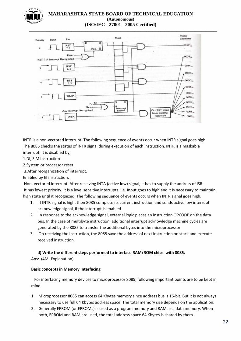
nonmaskable which means that it is not maskable by program control. The fig. shows the interrupt
structure of 8085. The fig indicates that, the 8085 is designed to response to edge triggering, level
triggering or both.
MAHARASHTRA STATE BOARD OF TECHNICAL EDUCATION (Autonomous)
(ISO/IEC - 27001 - 2005 Certified) _____________________________________________________________________________________________
22
INTR is a non-vectored interrupt .The following sequence of events occur when INTR signal goes high.
The 8085 checks the status of INTR signal during execution of each instruction. INTR is a maskable
interrupt. It is disabled by,
1.DI, SIM instruction
2.System or processor reset.
3.After reorganization of interrupt.
Enabled by EI instruction.
Non- vectored interrupt. After receiving INTA (active low) signal, it has to supply the address of ISR.
It has lowest priority. It is a level sensitive interrupts. i.e. Input goes to high and it is necessary to maintain
high state until it recognized. The following sequence of events occurs when INTR signal goes high.
1. If INTR signal is high, then 8085 complete its current instruction and sends active low interrupt
acknowledge signal, if the interrupt is enabled.
2. In response to the acknowledge signal, external logic places an instruction OPCODE on the data
bus. In the case of multibyte instruction, additional interrupt acknowledge machine cycles are
generated by the 8085 to transfer the additional bytes into the microprocessor.
3. On receiving the instruction, the 8085 save the address of next instruction on stack and execute
received instruction.
d) Write the different steps performed to interface RAM/ROM chips with 8085.
Ans: (4M- Explanation)
Basic concepts in Memory Interfacing
For interfacing memory devices to microprocessor 8085, following important points are to be kept in
mind.
1. Microprocessor 8085 can access 64 Kbytes memory since address bus is 16-bit. But it is not always
necessary to use full 64 Kbytes address space. The total memory size depends on the application.
2. Generally EPROM (or EPROMs) is used as a program memory and RAM as a data memory. When
both, EPROM and RAM are used, the total address space 64 Kbytes is shared by them.

MAHARASHTRA STATE BOARD OF TECHNICAL EDUCATION (Autonomous)
(ISO/IEC - 27001 - 2005 Certified) _____________________________________________________________________________________________
23
3. The capacity of program memory and data memory depends on the application.
4. It is not always necessary to select 1 EPROM and 1 RAM. We can have multiple EPROMs and
multiple RAMs as per the requirement of application.
For example:
We have to implement 32 Kbytes of program memory and 4 Kbytes EPROMs are available. In
this case, we can connect 8 EPROMs in parallel (4 Kbytes *8=32 Kbyte’s) with different chips select
for each EPROM.
5. We can place EPROM/RAM anywhere in full 64 Kbytes address space. But program memory
(EPROM) should be located from address 0000H since reset address of 8085 microprocessor is
0000H.
6. It is not always necessary to locate EPROM and RAM in consecutive memory addresses. For
example, if the mapping of EPROM is from 0000H to 0FFFH, it is not must to locate RAM
from 1000H. We can locate it anywhere between 1000H and FFFFH. Where to locate memory
component totally depends on the application.
The memory interfacing requires to:
a) Select the chip.
b) Identify the register.
c) Enable the appropriate buffer.
Microprocessor system includes memory devices and I/O devices. It is important to note that
microprocessor can communicate (read/ write) with only one device at a time, since the data,
address and control buses are common for all the devices. In order to communicate with memory
or I/O devices, it is necessary to decode the address from the microprocessor. Due to this each
device (memory or I/O) can be accessed independently. The following section describes common
address decoding techniques.
e) Draw block diagram of 8255 and explain the different blocks in brief.
Ans: (2M- Diagram 2M- explanation)

MAHARASHTRA STATE BOARD OF TECHNICAL EDUCATION (Autonomous)
(ISO/IEC - 27001 - 2005 Certified) _____________________________________________________________________________________________
24
Fig shows the internal block diagram of 8255A. It consist of data bus buffer, control logic and Group A and
Group B controls.
Data Bus Buffer
This tristate bidirectional buffer is used to interface the internal data bus of 8255 to the system data bus.
Input or output instructions executed by the CPU either read data from, or Write data into the buffer.
Output data from the CPU to the ports or control register, and input data to the CPU from the ports or
status register are all passed through the buffer.
Control Logic
The control logic block accepts control bus signals as well as inputs from the address bus, and issues
commands to the individual group control blocks (Group A control and Group B control). It issues
appropriate enabling signals to access the required data /control words or status word. The input pins for
the control logic section are described here.
Group A and Group B Controls
Each of the Group A and Group B control receives control words from the CPU and issues appropriate
command to the ports associated with it. The Group A control block controls Port A and PC7-PC4 while the
Group B control block controls Port B and PC3-PC0.
Port A: This has an 8 bit latched and buffered output and an 8 bit input latch. It can be programmed in
three modes: mode 0, mode1 and mode2.
Port B: This has an 8 bit data I/O latch/buffer and an 8 bit data input buffer. It can be programmed in
mode0 and mode1.
Port C: This has one 8-bit unlatched input buffer and an 8-bit output latch/buffer. Port C can be separated
into two parts and each can be used as control signals for ports A and B in the handshake mode. It can be
programmed for bit set/reset operation.
f) Compare 8255 with 8355(any four points).
Ans : (1M-each)
MAHARASHTRA STATE BOARD OF TECHNICAL EDUCATION (Autonomous)
(ISO/IEC - 27001 - 2005 Certified) _____________________________________________________________________________________________
25
Sr.No 8255 8355
1 It has 3 I/O ports: Port A, Port B, Port C It has 2 I/O ports: Port A, Port B,
2 It can operate in 3 modes:
Mode 0,Mode 1 ,Mode 2
Supports single mode: Simple I/O mode
3 DDR is not present Each I/O pin can be individually programmed
with the help of data direction register(DDR)
4 It doesn’t have memory. It has 2K of ROM
6. Attempt any FOUR of the following: 16
a) Explain the function of program counter and stack pointer in 8085.
Ans: (2M-each)
Program Counter (PC): Program is a sequence of instructions. As mentioned earlier, microprocessor
fetches these instructions from the memory and executes them sequentially. The program counter is a
special purpose register which, at a given time, stores the address of the next instruction to be fetched.
Program counter acts as a pointer to the next instructions. How processor increments program counter
depends on the nature of the instructions; for one byte instruction it increments program counter by two
and for three byte instructions it increments program counter by three such that program counter always
points to the address of the next instructions.
In case of JUMP and CALL instructions, address followed by JUMP and CALL instructions is placed
in the program counter. The processor then fetches the next instrucions from the new address
specified by JUMP or CALL instruction. In conditional JUMP and conditional CALL instructions, if the
condition is not satisfied, the processor increments program counter by three so that it points the
instruction followed by conditional JUMP or CALL instruction; otherwise processor fetches the next
instruction from the new address specified by JUMP or CALL instruction.
Stack Pointer (SP): The stack is a reserved area of the memory in the RAM where temporary information
may be stored. A 16 bit stack pointer is used to hold the address of the most recent stack entry.
b) Explain any four branching (conditional) instructions in 8085 by giving an example of each.
Ans: (1M- Each instruction ) (Any 4)
BRANCHING INSTRUCTIONS
Opcode Operand Description
1 .Jump unconditionally
JMP 16-bit address The program sequence is transferred to the memory location
specified by the 16-bit address given in the operand.
Example: JMP 2034H or JMP XYZ
2. Jump conditionally
Operand: 16-bit address
The program sequence is transferred to the memory location
MAHARASHTRA STATE BOARD OF TECHNICAL EDUCATION (Autonomous)
(ISO/IEC - 27001 - 2005 Certified) _____________________________________________________________________________________________
26
specified by the 16-bit address given in the operand based on
the specified flag of the PSW as described below.
Example: JZ 2034H or JZ XYZ
Opcode Description Flag Status
JC Jump on Carry CY = 1
JNC Jump on no Carry CY = 0
JP Jump on positive S = 0
JM J ump on minus S = 1
JZ Jump on zero Z = 1
JNZ Jump on no zero Z = 0
JPE Jump on parity even P = 1
JPO Jump on parity odd P = 0
3. Unconditional subroutine call
CALL 16-bit address : The program sequence is transferred to the memory location specified by the 16-bit
address given in the operand. Before the transfer, the address of the next instruction after CALL (the
contents of the program counter) is pushed onto the stack.
Example: CALL 2034H or CALL XYZ
4. Call conditionally
Operand: 16-bit address
The program sequence is transferred to the memory location specified by the 16-bit address given in the
operand based on the specified flag of the PSW as described below. Before the transfer, the address of the
next instruction after the call (the contents of the program counter) is pushed onto the stack.
Example: CZ 2034H or CZ XYZ
5. Return from subroutine unconditionally
RET The program sequence is transferred from the subroutine to the calling program. The
two bytes from the top of the stack are copied into the program counter, and program
execution begins at the new address.
Example: RET
6. Load program counter with HL contents
PCHL : The contents of registers H and L are copied into the program counter. The contents of H
are placed as the high-order byte and the contents of L as the low-order byte.
Example: PCHL
MAHARASHTRA STATE BOARD OF TECHNICAL EDUCATION (Autonomous)
(ISO/IEC - 27001 - 2005 Certified) _____________________________________________________________________________________________
27
7. Restart
RST 0-7 The RST instruction is equivalent to a 1-byte call instruction to one of eight memory
locations depending upon the number. The instructions are generally used in
conjunction with interrupts and inserted using external hardware. However these can
be used as software instructions in a program to transfer program execution to one of
the eight locations. The addresses are:
Instruction Restart Address
RST 0 0000H
RST 1 0008H
RST 2 0010H
RST 3 0018H
RST 4 0020H
RST 5 0028H
RST 6 0030H
RST 7 0038H
The 8085 has four additional interrupts and these interrupts generate RST instructions
internally and thus do not require any external hardware. These instructions and their
Restart addresses are:
Interrupt Restart Address
TRAP 0024H
RST 5.5 002CH
RST 6.5 0034H
RST 7.5 003CH
c) Write the different advantages of subroutines.
Ans: (Any Four – 1 Mark each)
Advantages of subroutines
1. Large programs are lined into modules.
2. Different modules of programs in the form of subroutine are written, tested and debugs separately.
3. It improves the efficiency or the program by reducing errors.
4. Repeated group of instruction are written into the subroutines are called whenever required in the main
program.
5. It save memory space and reduce time, size of program.
6. It reduces the time of market.
OR
In 8085 microprocessor a subroutine is a separate program written aside from main program, this program
is basically the program which requires to be executed several times in the main program. The
microprocessor can call subroutine any time using CALL instruction, after the subroutine is executed the
subroutine hands over the program to main program using RET instruction.
Advantages:
1. If a part of program appears repeatedly we may write it once and call it whenever required. This reduces
the size of the memory required for programs i.e it saves memory space.
2. If writing a large program then divide it in subsections, prepare and check each subsection separately
and at the end combine all the subsections using the main program. This makes the program modular. At a
MAHARASHTRA STATE BOARD OF TECHNICAL EDUCATION (Autonomous)
(ISO/IEC - 27001 - 2005 Certified) _____________________________________________________________________________________________
28
time different people work on individual subroutine. This improves efficiency, reduces time required for
programming.
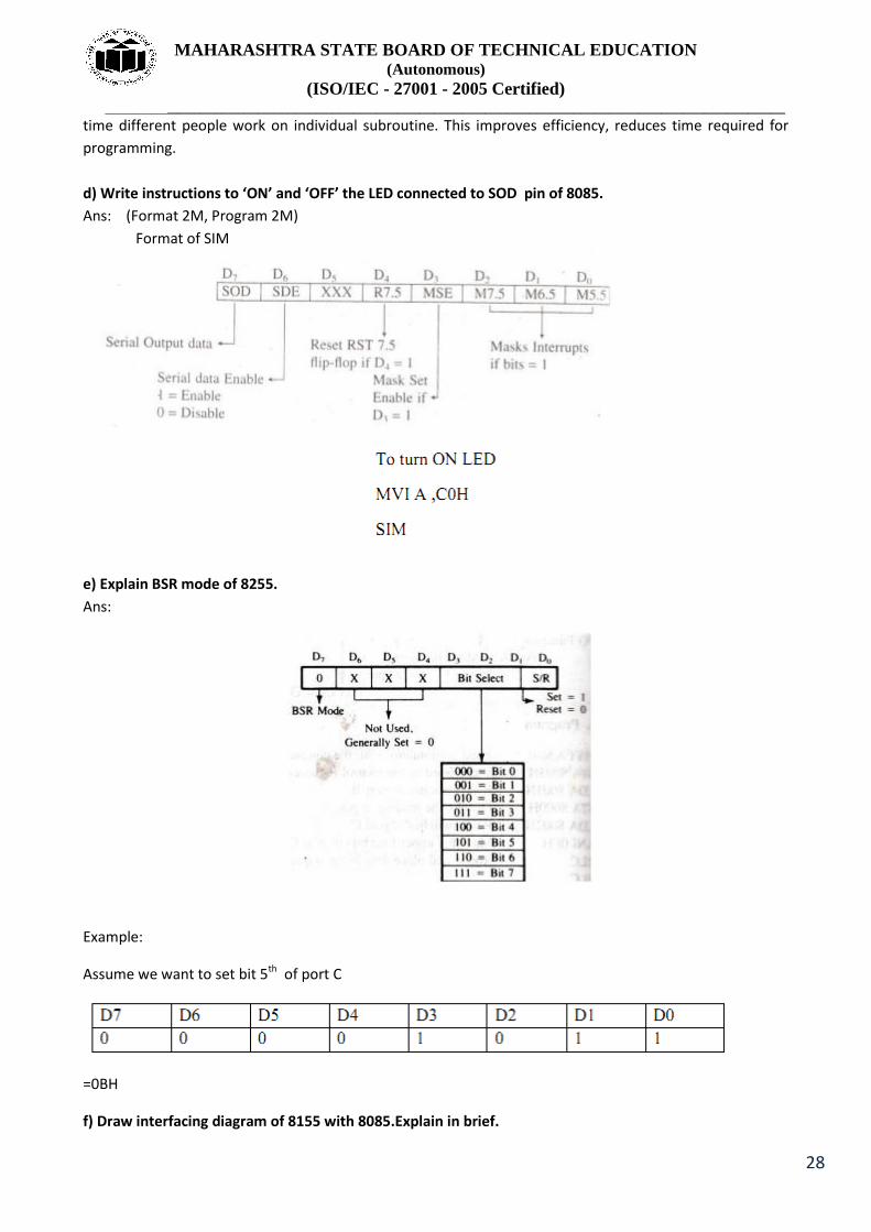
d) Write instructions to ‘ON’ and ‘OFF’ the LED connected to SOD pin of 8085.
Ans: (Format 2M, Program 2M)
Format of SIM
e) Explain BSR mode of 8255.
Ans:
Example:
Assume we want to set bit 5th of port C
=0BH
f) Draw interfacing diagram of 8155 with 8085.Explain in brief.

MAHARASHTRA STATE BOARD OF TECHNICAL EDUCATION (Autonomous)
(ISO/IEC - 27001 - 2005 Certified) _____________________________________________________________________________________________
29
Ans: 3M- diagram (any one) 1M for relevant explanation
Interfacing diagram of 8155 with 8085 in memory mapped I/O
Interfacing diagram of 8155 with 8085 in I/O mapped I/O

MAHARASHTRA STATE BOARD OF TECHNICAL EDUCATION (Autonomous)
(ISO/IEC - 27001 - 2005 Certified) _____________________________________________________________________________________________
30
============ ======== The End ======= =============