maharashtra state board of technical education (autonomous) (iso/iec...
TRANSCRIPT
MAHARASHTRA STATE BOARD OF TECHNICAL EDUCATION (Autonomous)
(ISO/IEC - 27001 - 2005 Certified)
SUMMER-14 EXAMINATION
Subject Code: 12189 Model Answer Page No: ____/ N
__________________________________________________________________________________________________
1/ 30
Important Instructions to examiners:
1) The answers should be examined by key words and not as word-to-word as given in the
model answer scheme.
2) The model answer and the answer written by candidate may vary but the examiner may try
to assess the understanding level of the candidate.
3) The language errors such as grammatical, spelling errors should not be given more
Importance (Not applicable for subject English and Communication Skills.
4) While assessing figures, examiner may give credit for principal components indicated in the
figure. The figures drawn by candidate and model answer may vary. The examiner may give credit for any
equivalent figure drawn.
5) Credits may be given step wise for numerical problems. In some cases, the assumed constant
values may vary and there may be some difference in the candidate’s answers and model answer.
6) In case of some questions credit may be given by judgement on part of examiner of relevant answer based on
candidate’s understanding. 7) For programming language papers, credit may be given to any other program based on equivalent concept.
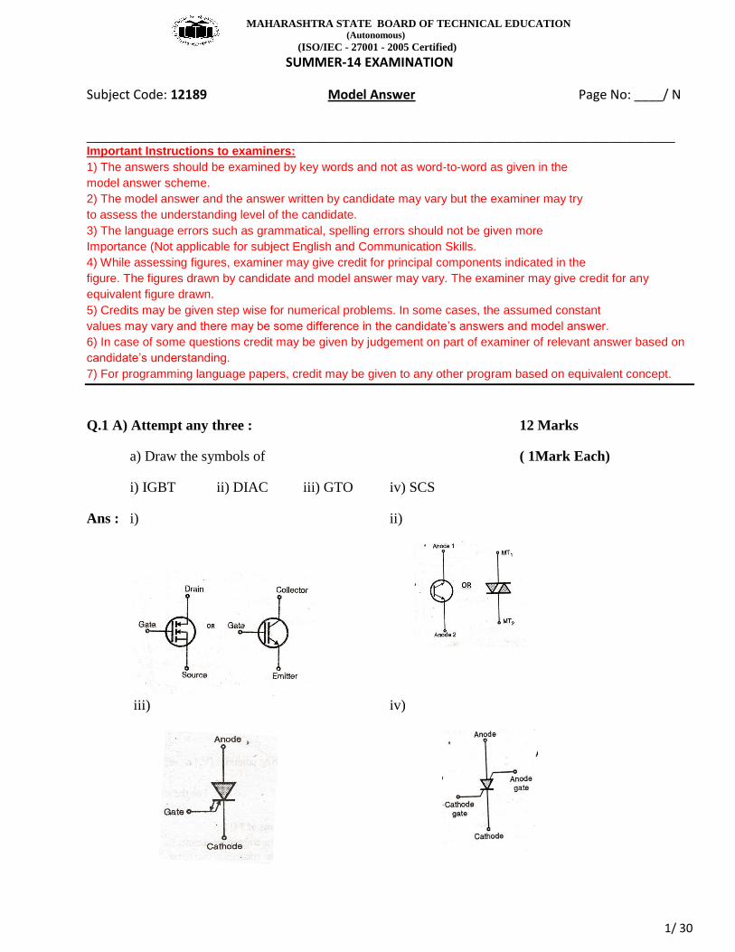
Q.1 A) Attempt any three : 12 Marks
a) Draw the symbols of ( 1Mark Each)
i) IGBT ii) DIAC iii) GTO iv) SCS
Ans : i) ii)
iii) iv)

MAHARASHTRA STATE BOARD OF TECHNICAL EDUCATION (Autonomous)
(ISO/IEC - 27001 - 2005 Certified)
SUMMER-14 EXAMINATION
Subject Code: 12189 Model Answer Page No: ____/ N
__________________________________________________________________________________________________
2/ 30
b) Explain the need and use of the poly phase rectifiers
Ans:
Use of polyphase rectifier: (2 Marks)
1)Number of phases are more due to that average output can be more.
2)In polyphase rectifier have less ripple so small filter can be used.
3) More DC power can be generated in motor control operation.
Need of polyphase rectifier: (2 Marks)
The average o/p voltage that can be obtained from single phase full wave rectifier is about 0.636 Vm &
can support power of the order of 1.5Kw To obtain higher power three phase line can be further
increased by connecting transformer windings to give intermediate phase shift. This increase in number
of phases increases the smoothness of o/p Dc. When simplest single phase HWR is used efficiency is
about 41% while for 3phase HWR efficiently increases to 97%. It is observed that as large number of
phases are used.
c) Why phase control rectifier are called as ac to dc converters? List the application of controlled
rectifiers.
Ans : (1 Marks)
These controller convert fixed ac voltage to a variable dc voltage. These converter takes power from one
or more ac voltage source of single or multiple phases and deliver to a load. The output variable is low
ripple dc voltage. These controller circuits used line voltage for their commutation. Hence they are also
called as line commutated or naturally commutated ac to dc converter.
Application : (3 Marks Any Three)
1. High voltage dc transmission system
2. DC motor drives.
3. Regulated dc power supply
4. Static VAR compensator
5. Wind generator converter
6. Battery charger circuits.

MAHARASHTRA STATE BOARD OF TECHNICAL EDUCATION (Autonomous)
(ISO/IEC - 27001 - 2005 Certified)
SUMMER-14 EXAMINATION
Subject Code: 12189 Model Answer Page No: ____/ N
__________________________________________________________________________________________________
3/ 30
d) Draw the construction of GTO and draw its V-I characteristics.
Ans : Construction of GTO ) (2 Marks)
V-I characteristics of GTO : (2 Marks)

MAHARASHTRA STATE BOARD OF TECHNICAL EDUCATION (Autonomous)
(ISO/IEC - 27001 - 2005 Certified)
SUMMER-14 EXAMINATION
Subject Code: 12189 Model Answer Page No: ____/ N
__________________________________________________________________________________________________
4/ 30
Q. 1 B) Attemptany One (6 Marks)
a) draw the static V-I characteristics of SCR. Name the various region on it. Define latching current ,
holding current and break over voltage of SCR.
Ans : V-I characteristics of SCR (2 Marks Charact. And 1 Mark mention region )
Latching current (IL):- (1 Marks)
It is minimum current whish is required to latch the device from off state to on state. It is
also can be defined as the minimum value of current required to trigger device.
Holding current (IH) :- (1 Marks)
It is minimum value of current required to hold conduction of the device. It may be
defined as minimum current below which device get off or stop conduction.
Break over voltage: (1 Marks)
It is a forward break over voltage when diode is conducted without gate, because to make device
forward bias should overcome junction barrier which is at reverse (J2) and which added with voltage
across J1 & J3 may be (0.6 + 0.6 + VB J2) when is VBR is depend on temperature ratio of and due to
reversed thermal operation and ICEO, which may be smaller than VBO.
MAHARASHTRA STATE BOARD OF TECHNICAL EDUCATION (Autonomous)
(ISO/IEC - 27001 - 2005 Certified)
SUMMER-14 EXAMINATION
Subject Code: 12189 Model Answer Page No: ____/ N
__________________________________________________________________________________________________
5/ 30
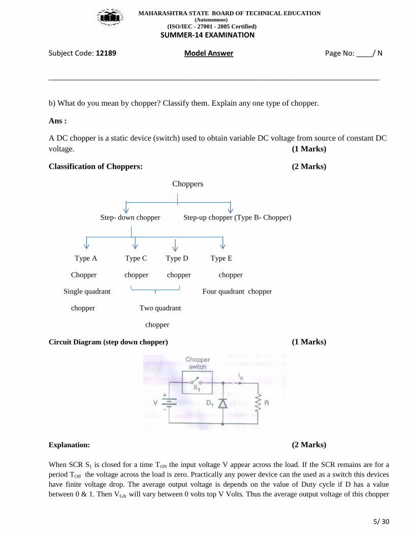
b) What do you mean by chopper? Classify them. Explain any one type of chopper.
Ans :
A DC chopper is a static device (switch) used to obtain variable DC voltage from source of constant DC
voltage. (1 Marks)
Classification of Choppers: (2 Marks)
Choppers
Step- down chopper Step-up chopper (Type B- Chopper)
Type A Type C Type D Type E
Chopper chopper chopper chopper
Single quadrant Four quadrant chopper
chopper Two quadrant
chopper
Circuit Diagram (step down chopper) (1 Marks)
Explanation: (2 Marks)
When SCR S1 is closed for a time TON the input voltage V appear across the load. If the SCR remains are for a
period TOff the voltage across the load is zero. Practically any power device can the used as a switch this devices
have finite voltage drop. The average output voltage is depends on the value of Duty cycle if D has a value
between 0 & 1. Then VLdc will vary between 0 volts top V Volts. Thus the average output voltage of this chopper
MAHARASHTRA STATE BOARD OF TECHNICAL EDUCATION (Autonomous)
(ISO/IEC - 27001 - 2005 Certified)
SUMMER-14 EXAMINATION
Subject Code: 12189 Model Answer Page No: ____/ N
__________________________________________________________________________________________________
6/ 30
circuit is always less than or equal to the input voltage. Hence this type of chopper is known as the step down
chopper.
OR
Circuit diagram (step up chopper) (1 Marks)
Explanation (2 Marks)
When SCR S1 is closed for time =t1, the inductor current rises and energy stored in the inductor, L. the
voltage across the inductor is equal to the input dc voltage V. during this time the output voltage will be
zero.
If SCR S1 is open circuited, then in order to maintained the inductor current the same direction there will
be an induced voltage across L. this voltage comes in series with the input DC voltage V. thus the total
voltage across SCR S1 is (V+voltage across inductor). The diode D1 is forward biased and the stored
energy in the inductance is transferred to the load.
Q. 2 Attempt any Four (16 Marks)
A) Explain two transistor analogy of SCR with neat diagram
Ans : Two transistor analogy (2 Marks)

MAHARASHTRA STATE BOARD OF TECHNICAL EDUCATION (Autonomous)
(ISO/IEC - 27001 - 2005 Certified)
SUMMER-14 EXAMINATION
Subject Code: 12189 Model Answer Page No: ____/ N
__________________________________________________________________________________________________
7/ 30
Explanation: (2 Marks)
The two transistor equivalent circuit shows that the collector current of the NPN transistor Q2 feeds
directly into the base of the PNP transistor Q1, while the collector current of TR1 feeds into the base of
Q2. These two inter-connected transistors rely upon each other for conduction as each transistor gets its
base-emitter current from the other‟s collector-emitter current. So until one of the transistors is given
some base current nothing can happen even if a Anode-to-Cathode voltage is present.
When the thyristors Anode terminal is negative with respect to the Cathode, the centre N-P junction is
forward biased, but the two outer P-N junctions are reversed biased and it behaves very much like an
ordinary diode. Therefore a thyristor blocks the flow of reverse current until at some high voltage level
the breakdown voltage point of the two outer junctions is exceeded and the thyristor conducts without
the application of a Gate signal. This is an important negative characteristic of the thyristor, as
Thyristors can be unintentionally triggered into conduction by an overvoltage as well as high
temperature or a rapidly rising dv/dt voltage such as a spike.
If the Anode terminal is positive with respect to the Cathode, the two outer P-N junctions are forward
biased but the center N-P junction is reverse biased. Therefore forward current is also blocked. If now a
positive current is injected into the base of the NPN transistor Q2, the resulting collector current flows in
the base of transistor Q1.This in turn causes a collector current to flow in the PNP transistor, Q1 which
increases the base current of Q2 and so on.
Very rapidly the two transistors force each other to conduct to saturation as they are connected in a
regenerative feedback loop. Once triggered into conduction, the current flowing through the device
between the Anode and the Cathode is limited only by the resistance of the external circuit. Then a
thyristor can be turned “ON” and made to act like a normal rectifying diode by the application of a
positive current to the base of transistor, TR2 which for a silicon controlled rectifier is called the “Gate”
terminal.
OR OR

MAHARASHTRA STATE BOARD OF TECHNICAL EDUCATION (Autonomous)
(ISO/IEC - 27001 - 2005 Certified)
SUMMER-14 EXAMINATION
Subject Code: 12189 Model Answer Page No: ____/ N
__________________________________________________________________________________________________
8/ 30
Once the thyristor has been turned “ON” and is conducting in the forward direction (anode positive), the
gate signal loses control due to the regenerative latching action of the two internal transistors. Then
applying a momentary Gate pulse to the device is enough to cause it to conduct and will remain
permanently “ON” even if the gate signal is completely removed. Then the thyristor can also be thought
of as a Bistable Switch having two states “ON” or “OFF”, as once it is triggered “ON” it cannot be
turned “OFF” again by its Gate
b) Draw the vertical structure of power transistor and explain it.
Ans : Vertical structure of power transistor :- (2 Marks)
Explanation: (2 Marks)
Fig. shows the doping level in each layer. The thickness of the different layer will have a significant
effect on the characteristics of the device. The emitter layer is heavily doped . the base is moderately
doped. The n- region is known as the collector drift region and it is lightly doped. The n
+ that terminates.
The drift region has doping level similar to that of emitter. This n+ region serves as collector contact.
Due to the low doping level the n- drift layer will increase the voltage blocking capacity of the transistor.
The width of this layer decide the breakdown voltage of power transistor.
The current gain β of a transistor depends on the base thickness. As the base thickness reduces the gain
increases but the breakdown voltage of transistor will decrease. In power transistor high breakdown
voltage is more important than high current gain. Therefore the base thickness is much larger than that in
the logic level transistor.
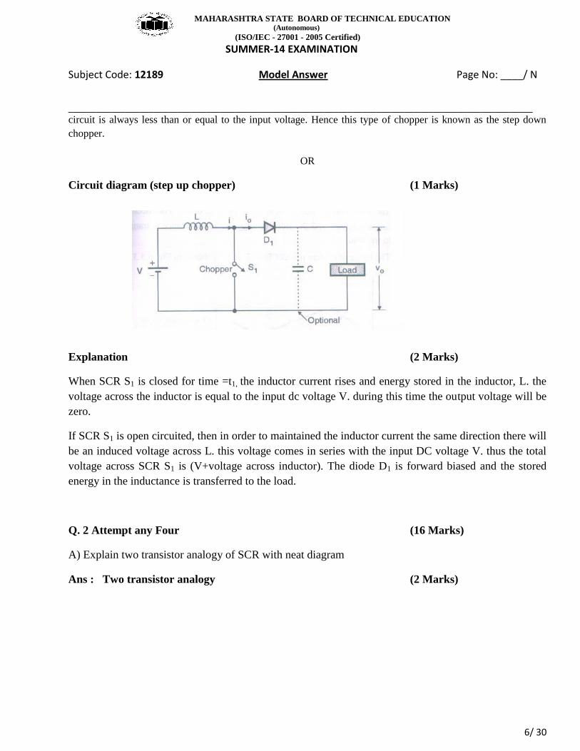
c) List the various forced commutation methods. Explain self commutation by resonating load.
Ans:
Forced commutation methods: (2 Marks)
1. Class A Self commutated by resonating the load.
2. Class B Self commutated by a LC circuit.
3. Class C Complementary commutation
MAHARASHTRA STATE BOARD OF TECHNICAL EDUCATION (Autonomous)
(ISO/IEC - 27001 - 2005 Certified)
SUMMER-14 EXAMINATION
Subject Code: 12189 Model Answer Page No: ____/ N
__________________________________________________________________________________________________
9/ 30
4. Class D Auxillary commutation
5. Class E an External pulse source for commutation
6. Class F AC line commutation
Circuit Diagram : (1 Marks)
Class A Self commutated by resonating the load.
Explanation: (1 Marks)
Class A turn off method:- for low values of R L& C are connected in series with R and for high
value of R Load R is connected across C, the essential required for this commutation circuit the overall
circuit must be under damped. The nature of the circuit should be such that when it is energised from
DC source current must have a natural tendency to zero for the load commutation to occur in thyristor
circuit. This class A commutation is also called as resonant commutation or self-commutation. When the
circuit is energized with DC source it is seen that current i is first rises to maximum value and then begin
to fall. When current decays to zero and tends to reverse thyristor turns off on its
d) Compare SCR and TRIAC ( any 4points)
Ans : (1 Marks Each point)
SCR TRIAC
1. Unidirectional 1. bidirectional
2. Terminal: gate, anode, cathode 2. Gate, mt1, mt2
OR

MAHARASHTRA STATE BOARD OF TECHNICAL EDUCATION (Autonomous)
(ISO/IEC - 27001 - 2005 Certified)
SUMMER-14 EXAMINATION
Subject Code: 12189 Model Answer Page No: ____/ N
__________________________________________________________________________________________________
10/ 30
3. Symbol:
3.
4. Application : specially converter
,inverter
4. Light dimmer,, ac speed controlled,
ac motor controlled
5. characteristics
5. characteristic
e) Draw the output waveform of 1 ¢ full controlled bridge converter with R-load for output voltage and
output current for firing angle. I) α =00 ii) α =90
0
Ans:- For α =00 ( 2 Marks)
α =900 ( 2Marks)
MAHARASHTRA STATE BOARD OF TECHNICAL EDUCATION (Autonomous)
(ISO/IEC - 27001 - 2005 Certified)
SUMMER-14 EXAMINATION
Subject Code: 12189 Model Answer Page No: ____/ N
__________________________________________________________________________________________________
11/ 30
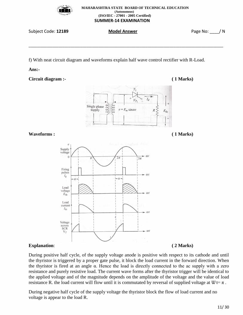
f) With neat circuit diagram and waveforms explain half wave control rectifier with R-Load.
Ans:-
Circuit diagram :- ( 1 Marks)
Waveforms : ( 1 Marks)
Explanation: ( 2 Marks)
During positive half cycle, of the supply voltage anode is positive with respect to its cathode and until
the thyristor is triggered by a proper gate pulse, it block the load current in the forward direction. When
the thyristor is fired at an angle α. Hence the load is directly connected to the ac supply with a zero
resistance and purely resistive load. The current wave forms after the thyristor trigger will be identical to
the applied voltage and of the magnitude depends on the amplitude of the voltage and the value of load
resistance R. the load current will flow until it is commutated by reversal of supplied voltage at Ѡ t= π .
During negative half cycle of the supply voltage the thyristor block the flow of load current and no
voltage is appear to the load R.

MAHARASHTRA STATE BOARD OF TECHNICAL EDUCATION (Autonomous)
(ISO/IEC - 27001 - 2005 Certified)
SUMMER-14 EXAMINATION
Subject Code: 12189 Model Answer Page No: ____/ N
__________________________________________________________________________________________________
12/ 30
Q 3 Attempt any Four : (16 Marks)
a) Describe Class-C commutation with the help of neat diagram.
Ans : Circuit diagram (2Marks )
Explanation (2Marks)
Here complementary SCR T2 is connected in parallel with the main SCR. Initially both the SCR are
OFF.
When a triggering pulse is applied to the gate of T1 the SCR T1 is triggered. Therefore current starts
flowing through the load as well as R2 & C. Capacitor C will get charged by the supply voltage Edc as
shown in figure.
When a triggering pulse is applied to the gate of T2 the SCR T2 is on, the negative polarity of the
capacitor C is applied to the anode of T1 & positive to the cathode. This causes the reverse voltage
across the main SCR T1 and immediately turns it off.
b) Explain 1 ф full converter with L-load with neat circuit diagram and necessary waveforms.
Ans: Circuit diagram ( 1 Marks)

MAHARASHTRA STATE BOARD OF TECHNICAL EDUCATION (Autonomous)
(ISO/IEC - 27001 - 2005 Certified)
SUMMER-14 EXAMINATION
Subject Code: 12189 Model Answer Page No: ____/ N
__________________________________________________________________________________________________
13/ 30
Explanation (2 Marks)
Here the conduction does not takes place until the SCRs are fired and in order for current to flow, SCRs
T1 & T2 must be fired together and SCRs T3 & T4 in the next half cycle. To ensuring simultaneous firing
both SCRs T1 & T2 are fired from the same firing circuit.
At firing angle α = 600 SCRs T1 & T2 are triggered. Current flows through the path L – T1 – A – L – R
– B – T2 - N. Supply voltage from this instant appears across output terminal & forces the current
through load. This load current Id is assumed to be constant. This current also flows through the supply
& the direction is from line to neutral, which is taken positive. At instant π voltage reverses. However
because of very large inductance L. the current is maintained in the same direction at instant constant
magnitude Id which keeps the SCRs T1 & T2 in conducting state and hence, the negative supply voltage
appears across output terminals.
At an angle Ω + α SCRs T3 & T4 are fired. With this the negative line voltage reverse biases SCRs T1 &
T2. The current flows through the path N – T3 – A- L – R – B – T4 – L. This continues in every halt
cycle and we get the output voltage as shown in the fig.
Waveforms ( 1 Marks)
c) List the various gate triggering methods of SCR. What do you mean by synchronization in triggering?
Draw the circuit of synchronized SCR gate triggering using UJT.
Ans:
Gate triggering methods of SCR:- ( 1 Mark)
1. D.C. gate triggering :
2. A.C. gate triggering
3. Pulse gate triggering

MAHARASHTRA STATE BOARD OF TECHNICAL EDUCATION (Autonomous)
(ISO/IEC - 27001 - 2005 Certified)
SUMMER-14 EXAMINATION
Subject Code: 12189 Model Answer Page No: ____/ N
__________________________________________________________________________________________________
14/ 30
Synchronization:- ( 1 Marks)
As the zener diode voltage Vz goes to zero at the end of each half cycle, the synchronization of the
trigger circuit with the supply voltage across SCR is achieved. Thus the time „t‟ when the pulse is
applied to SCR for the first time in each half cycle will remain constant for the same value of R
The circuit of synchronized SCR gate triggering using UJT:- ( 2 Marks)
d) State the function of free wheel diode in controlled rectifier with neat sketch.
Ans: Diagram ( 2 Marks)
Functions of free wheel diode: ( 2 Marks)
i) It prevents reversal of load voltage except for small diode voltage – drop.
ii) It transfers the load current away from the main rectifier, thereby allowing all of its thyristors to
regain their blocking states.

MAHARASHTRA STATE BOARD OF TECHNICAL EDUCATION (Autonomous)
(ISO/IEC - 27001 - 2005 Certified)
SUMMER-14 EXAMINATION
Subject Code: 12189 Model Answer Page No: ____/ N
__________________________________________________________________________________________________
15/ 30
e) Draw the symbol and construction of LASCR and describe it in brief.
Ans: Symbol Construction (1Marks Each)
Explanation ( 2marks)
It is SCR which will be turned on only when light falls on it because it is made from a material which is
light sensitive. Its symbol is shown in the diagram. It is having three junction and three terminals Anode,
Cathode and Gate.
As the light falls on LASCR this light energy generate large number of electrons and holes in the
junction J2 and current starts conducting because when LASCR is in the forward bias junction J1 and J3
are already forward biased so the device start conducting and the current increases rapidly which latch
the LASCR in the On state
f) Describe with neat ckt. Diagram and waveforms of the inverting mode operation of 1 ϕ full wave
controlled bridge rectifier.
Ans: Circuit diagram ( 1 mark)

MAHARASHTRA STATE BOARD OF TECHNICAL EDUCATION (Autonomous)
(ISO/IEC - 27001 - 2005 Certified)
SUMMER-14 EXAMINATION
Subject Code: 12189 Model Answer Page No: ____/ N
__________________________________________________________________________________________________
16/ 30
Waveforms ( 1 marks)
Explanation ( 2 marks)
Here firing pulses are retarded by an angle of 135 . The D.C. terminal voltage waveform now contains a
mean negative component & the fundamental component of the A.C. line current waveform lags the
voltage by an angle 135 . Since the mean D.C. terminal voltage is negative (α>90 the D.C. power and
hence also the mean A.C. power must also be negative. In other words power must also be negative. In
other words power is now being delivered from the D.C. side of the convertor to the A.C. side, and the
convertor is operating as a “line commutated invertor.”

MAHARASHTRA STATE BOARD OF TECHNICAL EDUCATION (Autonomous)
(ISO/IEC - 27001 - 2005 Certified)
SUMMER-14 EXAMINATION
Subject Code: 12189 Model Answer Page No: ____/ N
__________________________________________________________________________________________________
17/ 30
Q. 4 A) Attempt any three
a) Explain the necessity of specifying SOA by manufacturer. Also explain the second breakdown.
Ans:
Necessity of specifying SOA:- ( 2 Marks)
FBSOA:- During turn on and on state conditions, the average junction temperature and second
breakdown limit the power handling capacity of a transistor. The manufacturers uasualy provide the
FBSOA curves under specified test conditions. FBSOA indicates the IC - VCE limit of the transistor
and for reliable operation the transistor must not be subjected to greater power dissipation than that
shown by the FBSOA curve.
RBSOA:- During turn off a high current and high voltage must be sustained by the transistor, in most
cases with the base to emitter junction reverse bias. The collector emitter voltage must be held to a
safe level at or below a specified value of collector current. Tme manufacturers provide the IC - VCE
limits during reverse bias turn off as RBSOA..
Second Breakdown:- ( 2 Marks)
It is a destructive phenomenon, result from the current flow to a small portion of the base producing
localized hot spots. If the energy in these hot spots is sufficient the excessive localized heating may
damage the transistor. The secondary breakdown is caused by a localized thermal runway, resulting
from high current concentration. The current concentration may be caused by the defect in the transistor
structure.
b) Explain class A commutation with neat circuit diagram and waveforms.
Ans: Circuit diagram ( 1 mark)
OR

MAHARASHTRA STATE BOARD OF TECHNICAL EDUCATION (Autonomous)
(ISO/IEC - 27001 - 2005 Certified)
SUMMER-14 EXAMINATION
Subject Code: 12189 Model Answer Page No: ____/ N
__________________________________________________________________________________________________
18/ 30
Waveforms ( 1 Mark)
Explanation ( 2 marks)
In this process of commutation the forward current passing through the device is reduced to less than the
level of holding current of the device.
When the SCR is turned on by a gate pulse, an oscillatory current i flows in the circuit and charges up
the capacitor C. Capacitor C is charged up to the supply voltage Edc as the oscillatory current reaches its
peak value. Further capacitor charges from Edc value to 2Edc because inductor induces Edc voltage in the
capacitor. When the capacitor is completely charged up to 2 Edc, a differential voltage of ( 2Edc – Edc) =
Edc appear across the capacitor reflects at the cathode of the SCR and turns it off.
MAHARASHTRA STATE BOARD OF TECHNICAL EDUCATION (Autonomous)
(ISO/IEC - 27001 - 2005 Certified)
SUMMER-14 EXAMINATION
Subject Code: 12189 Model Answer Page No: ____/ N
__________________________________________________________________________________________________
19/ 30
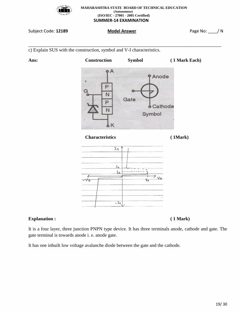
c) Explain SUS with the construction, symbol and V-I characteristics.
Ans: Construction Symbol ( 1 Mark Each)
Characteristics ( 1Mark)
Explanation : ( 1 Mark)
It is a four layer, three junction PNPN type device. It has three terminals anode, cathode and gate. The
gate terminal is towards anode i. e. anode gate.
It has one inbuilt low voltage avalanche diode between the gate and the cathode.

MAHARASHTRA STATE BOARD OF TECHNICAL EDUCATION (Autonomous)
(ISO/IEC - 27001 - 2005 Certified)
SUMMER-14 EXAMINATION
Subject Code: 12189 Model Answer Page No: ____/ N
__________________________________________________________________________________________________
20/ 30
d) Compare R and RC triggering methods of thyristors (any 4 points)
Ans: ( Each Point 1 Mark)
Parameter R triggering RC triggering
Components used Resistor Resistor and Capacitor
Maximum firing angle Cannot be greater than 900 Can be changed from 0
0 to 180
0
Isolation of control circuit and
power circuit
Not possible Not possible
Effect of supply fluctuations α changes α changes
Type of triggering AC gate triggering AC gate triggering
Circuit Diagram
Waveforms
MAHARASHTRA STATE BOARD OF TECHNICAL EDUCATION (Autonomous)
(ISO/IEC - 27001 - 2005 Certified)
SUMMER-14 EXAMINATION
Subject Code: 12189 Model Answer Page No: ____/ N
__________________________________________________________________________________________________
21/ 30
B) Attempt any one : ( 6 Mark)
a) Draw M2 ( mid – point) converter with L-Load. Explain with waveforms for the firing pulses. Load
voltage, load current and voltage across thyristors.
Answer: Circuit Diagram. ( 2 Marks)
Wave forms: ( 2 Marks)
MAHARASHTRA STATE BOARD OF TECHNICAL EDUCATION (Autonomous)
(ISO/IEC - 27001 - 2005 Certified)
SUMMER-14 EXAMINATION
Subject Code: 12189 Model Answer Page No: ____/ N
__________________________________________________________________________________________________
22/ 30
Explanation: ( 2 Marks)
With reference to above fig SCR T1 can be fired into the on state at any time after e1 goes positive. Once
SCR T1 is turned on current builds up in the inductive load, maintaining SCR T1 in the on state upto the
period when e1 goes negative. Since the load consists of inductance & resistance the w/f will be different
from that obtained with a pure resistive load. In this case as the AC voltage passes through natural zero
after negative half cycle, At negative half cycle SCR T2 will on after gate is trigger.
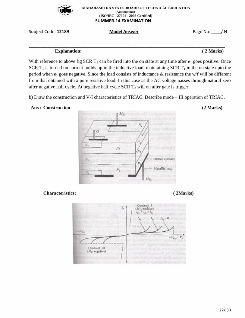
b) Draw the construction and V-I characteristics of TRIAC. Describe mode – III operation of TRIAC.
Ans : Construction (2 Marks)
Characteristics: ( 2Marks)

MAHARASHTRA STATE BOARD OF TECHNICAL EDUCATION (Autonomous)
(ISO/IEC - 27001 - 2005 Certified)
SUMMER-14 EXAMINATION
Subject Code: 12189 Model Answer Page No: ____/ N
__________________________________________________________________________________________________
23/ 30
Explanation: ( 2 Marks)
When terminal MT2 is negative and terminal MT1 is positive the device can be turned on by applying a
positive voltage between the gate and terminal MT1.
In this mode the device operates in the third quadrant when it is triggered into conduction. The turn on is
initiated by remote gate control. The main structure that leads to turn on is P2N1P1N4 with N2 acting as a
remote gate as shown in fig.
The external gate current IG forward biases P2N2 junction. Layer N2 injects electrons into P2 layer as
shown by dotted arrows and are collected by the junction P2N1. The electrons from N2 collected by P2N1
junction cause an increase of current through the junction P2 N1. The holes injected from P2, diffused
through N1 and arrived in P1. Hence a positive space charge builds a in the P1 region. More electrons
from N4 diffuse into P1 to neutralize the positive space charge. These electrons arrived at the junction J2.
They produced a negative space charge in the N1 region. Which results in more holes being injected
from P2 into N1.
This regenerative process continues until the structure P2N1P1N4 completely turns on and conducts the
current which is limited by the external load.
Q.5 Attempt any four (4x4=16)
a) Draw neat sketch of construction of IGBT and draw its V-I characteristics
Ans : Construction ( 2 Marks),
V-I characteristics ( 2 Marks)

MAHARASHTRA STATE BOARD OF TECHNICAL EDUCATION (Autonomous)
(ISO/IEC - 27001 - 2005 Certified)
SUMMER-14 EXAMINATION
Subject Code: 12189 Model Answer Page No: ____/ N
__________________________________________________________________________________________________
24/ 30
b) With neat circuit diagram and waveform explain symmetrical configuration of 1ф half controlled
bridge rectifier with R-load.
Ans: Circuit diagram (1 Marks)
Wave Form (2 marks)
Explanation (1 Mark)
Working –During +ve half cycle of the ac supply thyristor T1, and Diode D1, are forward biased and are
in forward Blocking mode. When the SCR T1 is triggered, at firing angle α , current flow through the
path L-T1-R-D1- N as shown in diagram, load current will flow until it is commutated by reversal of
supply voltage at Ѡt = π
During –ve half cycle of the ac supply T2 and D2 are forward biased When SCR T2 is triggered at an
angle (π+α), current would flow through the path N-T2 – R-D2-L load current is continuous till angle
2π,when SCR T2 is turned off.

MAHARASHTRA STATE BOARD OF TECHNICAL EDUCATION (Autonomous)
(ISO/IEC - 27001 - 2005 Certified)
SUMMER-14 EXAMINATION
Subject Code: 12189 Model Answer Page No: ____/ N
__________________________________________________________________________________________________
25/ 30
c) Compare natural commutation and forced commutation
Ans: [Any 4 points 4 Marks]
Sr.No. Parameter Natural Commutation Forced Commutation
1) Need of external
commutating
components
Not Necessary Necessary
2) Type of Supply AC DC
3) Power loss in
cumulating
components
NIL Some power loss takes
place
4) Type of Commutation SCR turns off due to anode
current going below IH or
due to the application of
reverse line voltage
Voltage commutation or
current commutation
5) Size of circuit Small due to absence of
commutating components
Big due to large
commutating components
6) Application In line commutated
converters and inverters
In series, parallel inverter,
chopper
d) Differentiate between 3ф half wave and 3ф full wave rectifiers with R-load with respect to
a) No. of diodes
b) PIV
c) Vdc
d) Ripple factor
Ans: (Each point 1 Mark)
Parameter 3 ф HWR 3 ф full wave rectifiers
a) No. of diodes 3 6
b) PIV Low High
c) Vdc Low High
d) Ripple factor High ripple factor Low ripple factor

MAHARASHTRA STATE BOARD OF TECHNICAL EDUCATION (Autonomous)
(ISO/IEC - 27001 - 2005 Certified)
SUMMER-14 EXAMINATION
Subject Code: 12189 Model Answer Page No: ____/ N
__________________________________________________________________________________________________
26/ 30
e) Compare 1ф half wave controlled rectifier and 1ф half controlled bridge rectifier
Ans: (Any 4 points)
Parameter 1ϕ half wave
controlled rectifier
1ϕ half controlled
bridge rectifier
No. of SCR One Two
No. of diodes No (zero) Two
Vdc Vdc = Vm/2π ( 1+cos) Vdc = Vm/π (1+cos)
Region of working In first quadrant In first quadrant
Ripple factor Large Less
Input power factor Very poor Good
Q.6 Attempt any Four : (16 Marks)
a) Draw neat diagram of 6 ф star half wave rectifier and explain it with neat waveforms.
Ans: Circuit diagram ( 1 Mark)
Wave forms (2 Mark)

MAHARASHTRA STATE BOARD OF TECHNICAL EDUCATION (Autonomous)
(ISO/IEC - 27001 - 2005 Certified)
SUMMER-14 EXAMINATION
Subject Code: 12189 Model Answer Page No: ____/ N
__________________________________________________________________________________________________
27/ 30
Working (1 Mark)
Phase voltages VRN VYN VBN are 120° out of phase with each other and VRN VYN VBN are 180°
phase shifted with respect to VRN VYN VBN respectively.
Diode which corresponds to maximum positive phase voltage would conduct, at any given
instant. At any given instant only one diode will be conduct and the load voltage will be equal to
the corresponding phase voltage with respect to N.
From waveform phase voltages cross each other at point 1, 2, 3…6 at these phase crossover
points incoming diodes will come into conduction and outgoing diode will be turn off.
b) Compare class – A and class – B commutation circuits.
Ans : ( Any 4 Points Each Point 1 Mark)
Parameter Class –A commutation Class –B commutation
Diagram
Position of the
commutating
components.
Commutating components are
connected in series with SCR
Commutating components are
connected in parallel with SCR
Load current Commutating components carry
load currents
Commutating components does
not carry load currents
Size and cost Due to commutating component
carry load current their size is
big, so circuit becomes bulky
and costly.
Size of circuit is small and cost
is less.
Application It is used in series inverter. It is used in DC chopper.
OR

MAHARASHTRA STATE BOARD OF TECHNICAL EDUCATION (Autonomous)
(ISO/IEC - 27001 - 2005 Certified)
SUMMER-14 EXAMINATION
Subject Code: 12189 Model Answer Page No: ____/ N
__________________________________________________________________________________________________
28/ 30
c) Draw the neat circuit diagram of parallel inverter and write its two applications.
Ans : Circuit diagram ( 5Mark)
Application ( Each ½ Mark)
1. Emergency system
2. In industrial application
3. High voltage dc transmission system
d) With the help of neat circuit diagram explain the resistance firing circuit and state its
limitations.
Ans : Circuit diagram ( 1 Mark)
Working :- ( 2 marks)
As es goes positive the SCR becomes forward biased from anode to cathode. It also forward
biased diode; this causes flow of a gate current Ig.

MAHARASHTRA STATE BOARD OF TECHNICAL EDUCATION (Autonomous)
(ISO/IEC - 27001 - 2005 Certified)
SUMMER-14 EXAMINATION
Subject Code: 12189 Model Answer Page No: ____/ N
__________________________________________________________________________________________________
29/ 30
Gate current will increase as es increase towards its peak value. When Ig reaches a value equal to
Ig[min] SCR turns on and eL = es.
SCR remains ON and eL = es until es decreases to the point where load current is below the SCR
holding current.
SCR turns off when es become negative. Since SCR is in reverse biased mode. It will act Ѡ open
switch and now load voltage is zero.
Same sequence is repeated when es again goes positive.
Limitations :- ( ½ Mark each)
1. Trigger angle α is greatly dependent on the SCR Ig(min)
2. Load voltage wave forms can only be varied from
e) Explain with neat circuit diagram and waveforms 1 ф controlled bridge rectifier with R-load.
Ans : Circuit Diagram ( 1 Mark)
Wave form ( 1 mark)
Working : ( 2 Mark)
During positive half cycle SCR1, SCR3 are forward biased and they are triggered
simultaneously, then current flows through the path L – SCR1 – RL – SCR3 – N.
During negative half cycle SCR2, SCR4 are forward biased and they are triggered
simultaneously, then current flows through the path N-SCR2 – RL –SCR4 –L.
When supply voltage falls to zero, SCR1, SCR3 in positive half cycle and SCR 2,SCR 4 in
negative half cycle turns off by natural commutation.

MAHARASHTRA STATE BOARD OF TECHNICAL EDUCATION (Autonomous)
(ISO/IEC - 27001 - 2005 Certified)
SUMMER-14 EXAMINATION
Subject Code: 12189 Model Answer Page No: ____/ N
__________________________________________________________________________________________________
30/ 30
f) Write the different turn ON methods of SCR. Explain thermal triggering of SCR.
Ans:
Turn on methods of SCR ( Any Four ½ mark Each)
1) Forward voltage triggering
2) Thermal Triggering
3) Radiation Triggering
4) Dv/dt triggering
5) Gate triggering
Thermal triggering ( 2marks)
Like any other semi-conductor, the width of the depletion layer of a thyristor decreases on increasing the
junction temperature. When the voltage applied between the anode and cathode is very near to its break
down voltage, the device can be triggered by increasing its junction temperature. This method of
triggering the device by heating is known as the thermal triggering process.