maharashtra state board of technical...
TRANSCRIPT

MAHARASHTRA STATE BOARD OF TECHNICAL EDUCATION (Autonomous)
(ISO/IEC - 27001 - 2005 Certified) _____________________________________________________________________________________________
1
Winter – 15 EXAMINATIONS
Subject Code: 17439 Model Answer
Important Instructions to examiners:
1) The answers should be examined by key words and not as word-to-word as given in the answer
scheme.
2) The model answer and the answer written by candidate may vary but the examiner may try to
assess the understanding level of the candidate.
3) The language errors such as grammatical, spelling errors should not be given more Importance
(Not applicable for subject English and Communication Skills.
4) While assessing figures, examiner may give credit for principal components indicated in the
figure. The figures drawn by candidate and model answer may vary. The examiner may give
credit for any equivalent figure drawn.
5) Credits may be given step wise for numerical problems. In some cases, the assumed constant
values may vary and there may be some difference in the candidate‟s answers and model
answer.
6) In case of some questions credit may be given by judgment on part of examiner of relevant
answer based on candidate‟s understanding.
7) For programming language papers, credit may be given to any other program based on
equivalent concept.

MAHARASHTRA STATE BOARD OF TECHNICAL EDUCATION (Autonomous)
(ISO/IEC - 27001 - 2005 Certified) _____________________________________________________________________________________________
2
Q.1 a) Attempt any SIX of the following 12 Marks
(i) Define: 1) Analog Signal
2) Digital Signal
Ans: (Any relevant correct definition - 1 mark each)
Analog Signal: A signal whose amplitude can take on any value in a continuous range is known as
an analog signal.
(OR)
A signal whose amplitude changes with respect to time is called as an analog signal.
Digital Signal: A signal whose amplitude can take on only a finite number of values is called as a
digital signal.
(ii) Compare amplitude modulation and frequency modulation. (Any two points)
Ans: (any two correct points – 1 mark each) (Other relevant correct points to be considered)
(iii) Explain the effect of fading on transmission of signals.
Ans: (any two relevant correct points – 1 mark each)
1. Rapid changes in signal strength over a small travel distance or time interval.
2. Random frequency modulation due to varying Doppler shifts on different multipath signals.
3. Time dispersion or echoes caused by multipath propagation delays.
(iv) Calculate image frequency if signal frequency is 2000 kHz & intermediate frequency is 650
kHz.
Ans: (formula – 1 mark, final answer – 1 mark)
Given: Signal frequency (fs) = 2000 kHz; Intermediate frequency (IF) = 650 kHz
To find: Image Frequency (fsi) = fs + 2IF
Solution: fsi = fs + 2IF = 2000 x 103 + 2 x (650 x 10
3) = 3300 kHz

MAHARASHTRA STATE BOARD OF TECHNICAL EDUCATION (Autonomous)
(ISO/IEC - 27001 - 2005 Certified) _____________________________________________________________________________________________
3
(v) Draw the radiation pattern of loop antenna.
Ans: (correct radiation pattern – 2 marks)
Note: antenna not be considered in marks it’s just for orientation
(vi) State Grass man‟s Law and its significance.
Ans: (statement – 1 mark, any two significance – 1 mark)
Statement: - “Eye perceives new colour depending on the algebraic sum of red , green & blue light
fluxes. This forms the basis of colour signal generation & is known as grass man‟s law.”
The eye is not able to distinguish each of the colours that are mixed to form colour but instead
perceives only resultant colour.
Significance of Grass man‟s Law:
White has been seen to be produced by adding red, green, blue lights.
Intensity of each colour may be varied.
This enables simple rules of addition and subtraction.
As additive mixing of three primary colours produces white colour, their subtraction produces
black colour.
(vii) Compare vidicon and plumbicon camera tubes w.r.t principle and advantage.
Ans: (each correct point – 1 mark)
Sr. No Parameter Vidicon Plumbicon
1 Principle It works on principle of
photoconductivity, where the
conductivity or resistivity of the
photosensitive surface varies in
proportion to the intensity of light
focused on it. The variations in
resistance at each point across the
surface of material develop a
varying electrical signal.
Plumbicon camera tube works on the
principle of photoconductivity,
where the resistance of target
materials decreases when exposed to
light.
2 Advantage Simple Construction, high
resistivity in dark
High sensitivity, low dark current
(viii) State the application of HDTV.
Ans: (any relevant correct points – 1 mark each)
Applications of HDTV:
1. Display device in Video Conferencing.
2. Display device in railway stations, hospitals, research labs and institutions etc.
3. Broadcasting TV channels.
MAHARASHTRA STATE BOARD OF TECHNICAL EDUCATION (Autonomous)
(ISO/IEC - 27001 - 2005 Certified) _____________________________________________________________________________________________
4
Q 1. b) Attempt any TWO of the following 8 Marks
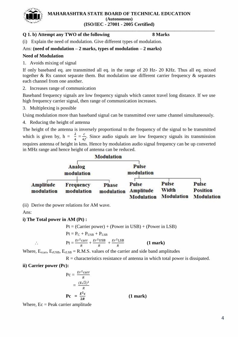
(i) Explain the need of modulation. Give different types of modulation.
Ans: (need of modulation – 2 marks, types of modulation – 2 marks)
Need of Modulation
1. Avoids mixing of signal
If only baseband eq. are transmitted all eq. in the range of 20 Hz- 20 KHz. Thus all eq. mixed
together & Rx cannot separate them. But modulation use different carrier frequency & separates
each channel from one another.
2. Increases range of communication
Baseband frequency signals are low frequency signals which cannot travel long distance. If we use
high frequency carrier signal, then range of communication increases.
3. Multiplexing is possible
Using modulation more than baseband signal can be transmitted over same channel simultaneously.
4. Reducing the height of antenna
The height of the antenna is inversely proportional to the frequency of the signal to be transmitted
which is given by, h =
=
. Since audio signals are low frequency signals its transmission
requires antenna of height in kms. Hence by modulation audio signal frequency can be up converted
in MHz range and hence height of antenna can be reduced.
(ii) Derive the power relations for AM wave.
Ans:
i) The Total power in AM (Pt) :
Pt = (Carrier power) + (Power in USB) + (Power in LSB)
Pt = PC + PUSB + PLSB
Pt =
+
+
(1 mark)
Where, Ercarr, ErUSB, ErLSB = R.M.S. values of the carrier and side band amplitudes
R = characteristics resistance of antenna in which total power is dissipated.
ii) Carrier power (Pc):
Pc =
= √
Pc =
(1 mark)
Where, Ec = Peak carrier amplitude

MAHARASHTRA STATE BOARD OF TECHNICAL EDUCATION (Autonomous)
(ISO/IEC - 27001 - 2005 Certified) _____________________________________________________________________________________________
5
iii) Power in sidebands:
The power in USB and LSB is same as,
PUSB = PLSB =
Peak amplitude of sideband =
PUSB = PLSB = √
=
PUSB = PLSB =
X
Since
= Pc
PUSB = PLSB =
Pc (1 mark)
iv) Total power in AM :
The total power in AM is,
Pt = Pc + PUSB + PLSB
= Pc +
Pc +
Pc
Pt = (1 +
) Pc (1 mark)
(iii) Define Pre-emphasis and de-emphasis with typical circuit diagram.
Ans: (each definition – 1 mark, typical circuit diagram – 1 mark each)
Pre-emphasis
The artificial boosting of higher audio modulating frequencies in accordance with prearranged
response curve is called pre-emphasis.
De-emphasis
The artificial boosting of higher modulating frequencies in the process of pre-emphasis is nullified
at receiver by process called de-emphasis. The artificially boosted high frequency signals are
brought to their original amplitude using de-emphasis circuit.
MAHARASHTRA STATE BOARD OF TECHNICAL EDUCATION (Autonomous)
(ISO/IEC - 27001 - 2005 Certified) _____________________________________________________________________________________________
6
Q 2. Attempt any FOUR of the following 16 marks
a) For AM transmission having carrier power 20kW is modulated to a depth of 50%. Calculate
1) total transmitted power 2) Power in each side band.
Ans: (each formula 1 mark, correct final answer – 1 mark each)
Given: Carrier Power (Pc) = 20 x 103 watt
Modulation index (m) = 0.5
To find: Total Transmitted Power (Pt)
Power in each side band (PUSB/PLSB)
Solution:
Power in each side band = (PUSB/PLSB) =
x Pc = 1.25 kW
Total Transmitted Power (Pt) = Pc [
] = 20 x 10
3 x [1.125] = 22.5 kW
(OR)
Total Transmitted Power (Pt) = Pc + PUSB + PLSB = 20 kW + 1.25 kW + 1.25 kW= 22.5 kW
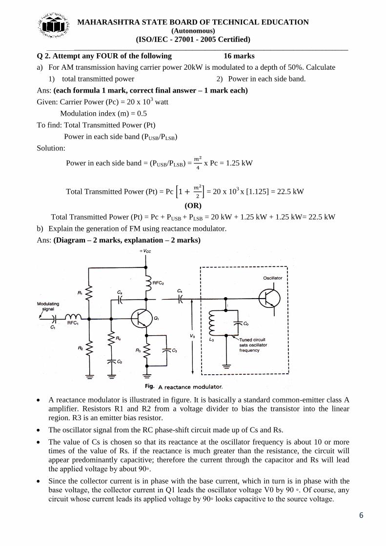
b) Explain the generation of FM using reactance modulator.
Ans: (Diagram – 2 marks, explanation – 2 marks)
A reactance modulator is illustrated in figure. It is basically a standard common-emitter class A
amplifier. Resistors R1 and R2 from a voltage divider to bias the transistor into the linear
region. R3 is an emitter bias resistor.
The oscillator signal from the RC phase-shift circuit made up of Cs and Rs.
The value of Cs is chosen so that its reactance at the oscillator frequency is about 10 or more
times of the value of Rs. if the reactance is much greater than the resistance, the circuit will
appear predominantly capacitive; therefore the current through the capacitor and Rs will lead
the applied voltage by about 90◦.
Since the collector current is in phase with the base current, which in turn is in phase with the
base voltage, the collector current in Q1 leads the oscillator voltage V0 by 90 ◦. Of course, any
circuit whose current leads its applied voltage by 90◦ looks capacitive to the source voltage.

MAHARASHTRA STATE BOARD OF TECHNICAL EDUCATION (Autonomous)
(ISO/IEC - 27001 - 2005 Certified) _____________________________________________________________________________________________
7
The modulating signal is applied to the modulator circuit through C1 and RFC1. The RFC helps
keep the RF signal from the oscillator out of the audio circuit from the modulating signal
usually comes. The audio modulating signal will vary the base voltage and current of Q1
according to the intelligence to be transmitted.
The collector current will also vary in proportion. As the collector current amplitude varies, the
phase shift angle changes with respect to the oscillator, voltage, which is interpreted by the
oscillator as a change in the capacitance. So as the modulating signal changes, the effective
capacitance of the circuit varies and the oscillator frequency is varied accordingly.
An increase in capacitance lowers the frequency, whereas a lower capacitance increases the
frequency. The circuit produces direct frequency modulations.
c) Define Noise. Give the causes and effects of Thermal Noise.
Ans: (definition – 2 mark, causes and effects – 2 marks)
Noise is defined as any unwanted signal interrupting the actual information signal which changes
the characteristics of the original signal.
Causes of Thermal Noise (any two)
Conductors contain a large number of 'free" electrons and "ions" strongly bound by molecular
forces. The ions vibrate randomly about their normal (average) positions, however, this
vibration being a function of the temperature.
Continuous collisions between the electrons and the vibrating ions take place. Thus there is a
continuous transfer of energy between the ions and electrons. This is the source of resistance in
a conductor.
The movement of free electrons constitutes a current which is purely random in nature and over
a long time averages zero. There is a random motion of the electrons which give rise to noise
voltage called thermal noise.
Thus noise generated in any resistance due to random motion of electrons is called thermal
noise or white or Johnson noise.
Effects of Thermal Noise
Due to the thermal noise the heat dissipation increases and this heat damages the surrounding
sensitive components.
d) Explain the generation of FM using IC 566.
Ans: (any relevant correct diagram & its respective explanation – 2 marks each)

MAHARASHTRA STATE BOARD OF TECHNICAL EDUCATION (Autonomous)
(ISO/IEC - 27001 - 2005 Certified) _____________________________________________________________________________________________
8
A common type of VCO available in IC form is NE/SE566. Referring to figure a timing
capacitor Ct is linearly charged or discharged by a constant current source/sink.
The amount of current can be controlled by charging the voltage Vc applying at the modulating
input (pin 5) or by changing the timing resistor Rt external to IC chip.
The voltage at pin 6 is held at the same voltage as pin5. Thus if the modulating voltage at pin 5
is increased the voltage at pin 6 also increases, resulting in less voltage across Rt and thereby
decreasing the charging current.
The output frequency of the VCO can be changed either by (i) Rt, (ii) Ct or (iii) The voltage Vc
at the modulating input terminal pin 5. The voltage Vc can be varied by connecting a R1R2
circuit is shown in figure.
The component Rt and Ct are first selected so that VCO output frequency lies in the centre of the
operating frequency range.
Now the modulating input voltage is usually varied from 0.75 Vcc to Vcc which can produce a
frequency variation of about 10 to 1.
(OR)
If a voltage-controlled capacitor is placed in the feedback loop of an oscillator and the modulation
signal is applied across this capacitor, then the oscillator will change in frequency and the resulting
output signal is an FM signal.
The LM 566 is a linear voltage-to-frequency converter which can generate an FM signal up to 1
MHz and for a +/- 10% deviation from the center frequency, it has an FM distortion of less than
0.2%. The center frequency (fo) is set by a resistor (Ro) and a capacitor (Co),
The LM 566 delivers either an FM square wave or an FM triangular wave. However, the
square/triangular wave can be converted into a sine wave with the use of a simple RC filter. The
input impedance for the modulation signal is 1 MΩ and the output impedance of the
square/triangular wave is 50 Ω.
In both cases above, if the modulating signal is a digital waveform, then the resulting FM signal is a
frequency-shift-keying signal (FSK)
MAHARASHTRA STATE BOARD OF TECHNICAL EDUCATION (Autonomous)
(ISO/IEC - 27001 - 2005 Certified) _____________________________________________________________________________________________
9
e) Discuss about the propagation of electromagnetic waves. Give different types of it.
Ans: (Propagation of EM waves – 2 marks, any four types of propagation – 2 marks)
Electromagnetic waves are the waves which comprises of electric field and magnetic field
components which are orthogonal to each other and these fields are orthogonal to the direction of
propagation.
Propagation of EM waves is nothing but the way in which these waves travel through a medium
(free space, sea/ocean, etc.).
They always travel in a straight line but may get easily diverted when they come across many
problems like dispersion, scattering, refraction and reflection.
These are the parameters which affect the propagation of electromagnetic waves.
The type of propagation is decided by the route taken by the signal to reach the receiver from the
transmitter.
The three routes that the radio signal can take to reach the receiver are:
1. Along the surface of the earth
2. Up to the layer called ionosphere and back
3. From transmitter to receiver in straight line (Line of sight)
The path taken by the EM waves depends on many factors including frequency of the signal,
atmospheric conditions and the time of day.
Types of Propagation:
1. Ground Wave Propagation
2. Space Wave Propagation
3. Sky Wave Propagation / Ionospheric Propagation
4. Duct Propagation
5. Tropospheric Scattering
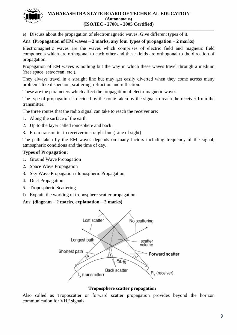
f) Explain the working of troposphere scatter propagation.
Ans: (diagram – 2 marks, explanation – 2 marks)
Troposphere scatter propagation
Also called as Troposcatter or forward scatter propagation provides beyond the horizon
communication for VHF signals

MAHARASHTRA STATE BOARD OF TECHNICAL EDUCATION (Autonomous)
(ISO/IEC - 27001 - 2005 Certified) _____________________________________________________________________________________________
10
Two directional antennas are pointed so that their beams intersect midway between them, above
the horizon.
One of these antennae is UHF transmitting antenna and the other a UHF receiving one, whereas
sufficient radio energy will be directed towards the receiving antenna to make this a useful
communication system.
The reasons for the scattering are not fully understood, but there are two theories behind this.
One suggest the reflections from 'blobs' in the atmosphere similar to the scattering of a search
light beam by duct particles and The other due to reflection from atmospheric layers.
This phenomenon is a permanent and not a sporadic one. The most commonly used are 900
MHz, 2000 and 5000 MHz.
The energy content of the forward scatter which is received by the receiver is very small of the
incident power. It is very small as one millionth of the incident power. Hence, a very high
transmitting power is required.
This method is used for long distance telephone and other communication links as an alternative
for microwave links or coaxial cables .Paths links are typically 300 to 500 Km long .
Q3. Attempt any FOUR of the following ( 16)
a) Compare PAM and PWM (any four points).
Ans:- (relevant any 4 points- 4 mks)
b) Describe the concept of actual height and virtual height.
Ans:- (Diagram - 2 mks, Definition - 1 mks each)

MAHARASHTRA STATE BOARD OF TECHNICAL EDUCATION (Autonomous)
(ISO/IEC - 27001 - 2005 Certified) _____________________________________________________________________________________________
11
c) Give two applications of horn antenna and dish antenna.
Ans:- (Any two relevant applications - 2 mks each)
Horn Antenna-1) As feed antenna
2) Satellite antenna
Dish Antenna-1) Satellite TV reception
2) Point to point microwave link
d) Distinguish between folded dipole and straight dipole antenna w.r.t construction I/P impedance,
radiation pattern and application.
Ans:- (Proper 4 mks for relevant answers)
Parameters Folded dipole antenna Straight dipole antenna
construction
A folded dipole is a dipole antenna
with the ends folded back around
and connected to each other,
forming a loop
A straight antenna is a resonant
antenna with length multiple of /2
and open on ends as shown
i/p impedance I/p Impedance is 4 times more than
straight dipole antenna
I/p impedance is less than folded
dipole antenna
Radiation pattern
application Used as the feeder element or
driven element of Yagi uda antenna
They are used as the parasitic
elements of Yagi uda antenna
MAHARASHTRA STATE BOARD OF TECHNICAL EDUCATION (Autonomous)
(ISO/IEC - 27001 - 2005 Certified) _____________________________________________________________________________________________
12
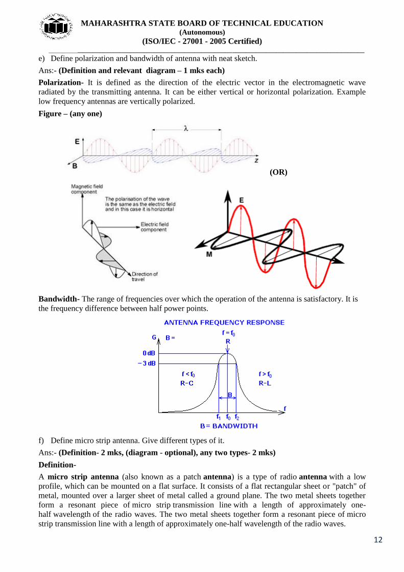
e) Define polarization and bandwidth of antenna with neat sketch.
Ans:- (Definition and relevant diagram – 1 mks each)
Polarization- It is defined as the direction of the electric vector in the electromagnetic wave
radiated by the transmitting antenna. It can be either vertical or horizontal polarization. Example
low frequency antennas are vertically polarized.
Figure – (any one)
(OR)
Bandwidth- The range of frequencies over which the operation of the antenna is satisfactory. It is
the frequency difference between half power points.
f) Define micro strip antenna. Give different types of it.
Ans:- (Definition- 2 mks, (diagram - optional), any two types- 2 mks)
Definition-
A micro strip antenna (also known as a patch antenna) is a type of radio antenna with a low
profile, which can be mounted on a flat surface. It consists of a flat rectangular sheet or "patch" of
metal, mounted over a larger sheet of metal called a ground plane. The two metal sheets together
form a resonant piece of micro strip transmission line with a length of approximately one-
half wavelength of the radio waves. The two metal sheets together form a resonant piece of micro
strip transmission line with a length of approximately one-half wavelength of the radio waves.

MAHARASHTRA STATE BOARD OF TECHNICAL EDUCATION (Autonomous)
(ISO/IEC - 27001 - 2005 Certified) _____________________________________________________________________________________________
13
(Optional)
Types- (any two)
1) Micro strip patch antenna
2) Micro strip slot antenna
3) Printed dipole antenna
4) PIFA- Planar inverted F antenna
5) FICA- Folded inverted conformal antenna
Q4. Attempt any FOUR of the following. 16 marks
a) Draw the block diagram of AM super- heterodyne radio receiver. Draw W/F of output of each
block.
Ans:- (any relevant correct diagram with waveforms – 4 marks)

MAHARASHTRA STATE BOARD OF TECHNICAL EDUCATION (Autonomous)
(ISO/IEC - 27001 - 2005 Certified) _____________________________________________________________________________________________
14
b) Define following characteristics of AM radio receiver:
i) Fidelity
ii) Selectivity
iii) Sensitivity
iv) Noise figure
Ans:- (Definition-1 mks each)
i) Sensitivity – It is defined as the ability of radio receiver to amplify weak signals. It is
measured in µV.
ii) Selectivity – It is defined as the ability if radio receiver to reject unwanted signals. It
decides the adjacent channel rejection of receiver.
iii) Fidelity – it is the ability of receiver to produce faithfully all the audio frequencies with
which the carrier is modulated. It is expressed in frequency response curve.
iv) Noise figure:- Noise figure (NF) is a measures of degradation of the signal-to-noise ratio
(SNR), caused by components in a radio frequency (RF) signal chain. It is a number by
which the performance of an amplifier or a radio receiver can be specified, with lower
values indicating better performance.
c) Draw and explain PLL as FM demodulator.
Ans:- (Diagram- 2mks, Explanation- 2mks)
Explanation-
Phase detector is basically a balanced modulator, produces an average (or low frequency) output
voltage that is linear function of the phase difference between the two input signals.
The frequency component is selected by the low-pass filter which also removes much of the
noise. The filtered signal is amplified by amplifier.
Amplified signal passed as a voltage to the VCO where it results in frequency modulation of the
VCO frequency.
FM signal which is to be demodulated is applied to input of PLL.VCO output must be identical
to input signal if PLL is to remain locked.
As PLL is locked, VCO starts tracking the instantaneous frequency in the FM input signal
The error voltage produced at the output amplifier is proportional to the deviation of input
frequency from centre frequency of FM.
Thus AC components of error voltage represent the modulation signal which is nothing but
demodulated FM output.

MAHARASHTRA STATE BOARD OF TECHNICAL EDUCATION (Autonomous)
(ISO/IEC - 27001 - 2005 Certified) _____________________________________________________________________________________________
15
d) Compare balanced slope detector and slope detector (any four points)
Ans:- (any relevant 4 points- 4 mks)
Parameters Slope detector Balance slope detector
Linearity of o/p characteristics Poor as it is linear over very
limited frequency range
Poor but better than slope
detector
Circuit components Simple –as it has Tank circuit
with proper RC load
Consists of two slope
detectors
Applications Not used in practice Not used in practice
Alignment/tuning Difficult to adjust the primary
and secondary windings of
transformer
Critical as three circuits need
to be tuned at different
frequencies
Efficiency poor More efficient
Amplitude limiting Not provided Not provided
e) Describe the working of delayed AGC circuit.
Ans: (circuit- 2 mks, graph 1 mks,explanation- 1 mks)

MAHARASHTRA STATE BOARD OF TECHNICAL EDUCATION (Autonomous)
(ISO/IEC - 27001 - 2005 Certified) _____________________________________________________________________________________________
16
f) Describe additive colour mixing. Draw additive colour circuit diagram.
Ans: (Circuit diagram- 2 mks, explanation-1 mks, diagram-1 mks)
Circuit diagram-

MAHARASHTRA STATE BOARD OF TECHNICAL EDUCATION (Autonomous)
(ISO/IEC - 27001 - 2005 Certified) _____________________________________________________________________________________________
17
Q5. Attempt any Four of the following 16 marks
a) Explain working of practical diode detector circuit.
Ans: (Circuit diagram 2M and working 2M)
Circuit:
Operation:
The diode has been reversed, so that now the negative envelop is demodulated.
Due to this negative envelope AGC voltage will be developed.
R1 and R2 ensure that there is a series DC path to ground for diode.
R1- C1 is the low pass filter used to remove RF ripple that is present in the detector output.
C2 is coupling capacitor that prevents the diode DC output from reaching the volume control
R4.
R3 – C3 is a low pass filter which removes AF components and help to produce AGC voltage.
The DC AGC voltage is proportional to the amplitude of AM signal.
b) Identify the blocks in above block diagram and state the function of missing blocks.
Ans: (Labeling each block 1M and Function of each block 1M)
i. If Amplifier: If signal is amplified by IF amplifier.
ii. Local oscillator: Tuning is done through local oscillator.
If = fo – fs
fo is local oscillator frequency.
MAHARASHTRA STATE BOARD OF TECHNICAL EDUCATION (Autonomous)
(ISO/IEC - 27001 - 2005 Certified) _____________________________________________________________________________________________
18
c) Define luminance, hue, saturation and compatibility as applied to colour T.V. system.
ANS: (Each 1M)
Luminance or brightness: This is the amount of light intensity as perceived by the eye regardless
of the colour. In black and white pictures, better lighted parts have more luminance than dark areas.
Hue: The colour itself is called „hue‟ and depends on the dominant wavelength of the light. By
adding two or more of the primary colours, many hues are produced. For example red and green
added in certain proportions that produce yellow.
By mixing red and blue in certain proportions, we obtain magneta and similarly by adding blue and
green colours in certain proportions we get cyan. Thus, red, green blue yellow are all hues.
I.e. Red + Green = Yellow
Red + Blue = Magenta
Blue + Green = Cyan
Saturation: It represents the purity of colour. It is the amount of white light mixed with colour. A
fully saturated colour will have no white light present in it. For example, pure red, blue, green i.e.
primary colours are saturated colours.
Compatibility: It is a phenomenon by which a colour TV system produces a normal B/W picture
on B/W TV receiver without any modification to existing circuitry.
Similarly, a B/W transmission should be able to produce a black and white picture on a colour TV
screen. This is known as reverse compatibility.
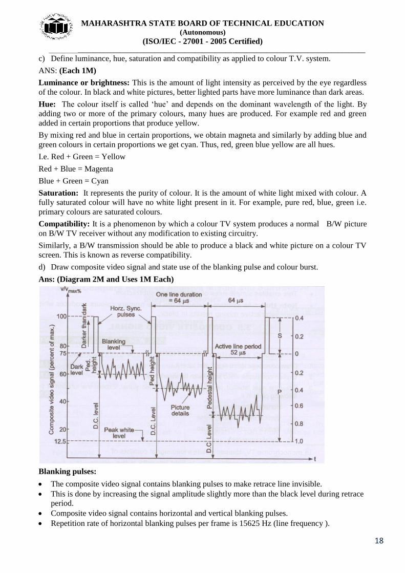
d) Draw composite video signal and state use of the blanking pulse and colour burst.
Ans: (Diagram 2M and Uses 1M Each)
Blanking pulses:
The composite video signal contains blanking pulses to make retrace line invisible.
This is done by increasing the signal amplitude slightly more than the black level during retrace
period.
Composite video signal contains horizontal and vertical blanking pulses.
Repetition rate of horizontal blanking pulses per frame is 15625 Hz (line frequency ).

MAHARASHTRA STATE BOARD OF TECHNICAL EDUCATION (Autonomous)
(ISO/IEC - 27001 - 2005 Certified) _____________________________________________________________________________________________
19
Vertical blanking pulse frequency is 50 Hz (field frequency).
Sync pulses are having amplitude in upper 25 percent of video signal.
Colour Burst:
The subcarrier is suppressed in the modulated signal (at transmitter), it is necessary to generate
it in the receiver for demodulation of the colour signal. This signal generated must be of exactly
same frequency and phase as that of the transmitter.
To ensure this, short wave of 8 to 10 pulse called the colour burst is placed or gated onto the
back porch of the blanking pulse of the composite video signal.
The burst signal acts as Pilot carrier.
Burst signal in conjunction with the phase comparator circuit in the receiver is used to lock the
local sub-carrier at the transmitter.
e) Explain interlaced scanning with neat sketch.
Ans: (Diagram 2M and Explanation 2M)
Interlaced scanning the process in which the first 312.5 odd numbered lines are scanned called odd
filed and then 312.5 even number lines are scanned, called even field so that frame containing 625
lines is scanned twice.
To achieve this, the horizontal sweep oscillator is made to work at a frequency of 15625 Hz ( i
e. 312.5 x 50 = 15625) to scan the number of lines per frame, but the vertical sweep circuit is
run at a frequency of 50 Hz ( i.e. 25 x 2 = 50 Hz).

MAHARASHTRA STATE BOARD OF TECHNICAL EDUCATION (Autonomous)
(ISO/IEC - 27001 - 2005 Certified) _____________________________________________________________________________________________
20
Note that since the beam is now deflected from top to bottom in half the time and horizontal
oscillator still operating at 15625 Hz, only half the total lines (i.e. 312.5) get scanned during
each vertical sweep.
Since the first field ends in a half line and the second field starts middle of the line on top of the
screen, (shown in figure)the beam is able to scan the remaining 312.5 alternate lines during its
down word journey.
The beam scans 625 lines per frame at the same rate of 15625 lines per second. Therefore, with
interlaced scanning the flicker effect is eliminated without increasing the speed of scanning,
which in turn does not need any increase in channel bandwidth.
f) State CCIR-B standards for colour signal transmission and reception.
Ans: (Any four correct points 1 mark each)
Parameters Standard
Number of lines per picture 625
Interlace ratio 2:1
Frame frequency 25
Field frequency 50
Aspect ratio 4:3
Line frequency 15625 Hz
Channel bandwidth 7 MHz
Video bandwidth 5 MHz
Sound carrier relative to picture carrier 5.5 MHz
Sideband completely transmitted Upper sideband
Type of sound modulation FM, ± 50 kHz
Resolution 400 lines
Duration of horizontal lines (H) 64 µs
Line blanking interval 12 µs
Front porch 1.5 µs
Back porch 5.8 µs
Camera output R, G and B video signals
Luminance signal Y = 0.30 R + 0.59 G + 0.11 B
Colour difference signals chosen for transmission (B – Y ) and ( R – Y )
Colour subcarrier frequency 4.433185 MHz
Duration of burst 10 ± 1
Chroma encoding Phase and amplitude modulation

MAHARASHTRA STATE BOARD OF TECHNICAL EDUCATION (Autonomous)
(ISO/IEC - 27001 - 2005 Certified) _____________________________________________________________________________________________
21
Q6. Attempt any FOUR of the following 16 marks
a) Describe the working principle of colour picture tube.
Ans: (Diagram 2M Working Principle 2M)
Principle:
Electron beams from the guns strike three phosphor dots of a triad. The dots of red, green and blue
phosphors in triad glow simultaneously the intensity of glow being proportional to the intensity of
video signal of the respective colour. The eye adds the three colours emitted by the phosphor dots at
a time and perceive the resultant colour of the concern pixel as the original picture.
The triads glow one after other in quick succession due to deflection of the beams and hence the
whole picture is reproduced in its original colour.
Working:
As shown in figure, the tube employs a screen where three colour phosphor dots are arranged in
groups known as triads.
Each phosphor dots corresponds to one of the three primary colours.
The triads are repeated and depends on the size of the picture tube, are deposited on the glass
phase plate (3, 33,000 triads).
A thin perforated metal sheet known as shadow mask is located 1 cm behind the tube screen.
The mask has one hole for every phosphor dot triad on the screen.
The various holes are so oriented that electrons of the three beams on passing through any one
whole will hit only the corresponding colour phosphor dots on the screen.
The ratio of the electrons passing through the holes to those reaching shadow masks is only
20%.
The remaining 80% of the total beam current, energy is dissipated as heat loss in shadow mask.
b) Describe use of equalizing pulses.
ANS: (Proper Description 4M)
Equalizing Pulses:
To take care of the drawback which occurs on account of the half line discrepancy, five narrow
pulses are added on either side of vertical sync pulses. These are known as pre-equalizing and
past equalizing pulses. Each set consist of five narrow pulses occupying 2.5 lines period on
either side of vertical sync pulses.
The effect of these pulses is to shift the half-line discrepancy away both from the beginning and
end of vertical sync pulses.
Pre-equalizing pulses are of 2.3 µs duration result in the discharge of capacitor to essentially
zero voltage in both the fields despite half-line discrepancy before the voltage built-up starts
with the arrival of vertical sync pulses.

MAHARASHTRA STATE BOARD OF TECHNICAL EDUCATION (Autonomous)
(ISO/IEC - 27001 - 2005 Certified) _____________________________________________________________________________________________
22
Post-equalizing pulses are necessary for a fast discharge of the capacitor to ensure triggering of
the vertical oscillator at proper time.
Thus, with the insertion of narrow pre- and post-equalizing pulses, the voltage rise and fall is
essentially the same for both the field sequences and the vertical oscillator is triggered at proper
instants.
c) Draw block diagram of MATV. Give any two application of it.
Ans: (Block diagram 2M Applications 2M)
Applications:
i. MATV system is used as community antenna to serve the TV receivers in the fringe or
shadow areas.
ii. It is also used as a common antenna to serve the flats in an apartment building or room in a
hotel or big institute or organization.
iii. MATV provides many other values added features to the people.
One or more antennas are located on roof top, the number depending on telecast and their
direction.
Each antenna is located in such direction that all stations are received simultaneously. MATV
system is design to have 75 Ω impedance so that match between co-axial line and components is
achieved.

MAHARASHTRA STATE BOARD OF TECHNICAL EDUCATION (Autonomous)
(ISO/IEC - 27001 - 2005 Certified) _____________________________________________________________________________________________
23
d) Explain home security application of CCTV system.
Ans: (Explanation 2M Diagram 2M)
Explanation:
As the name implies, it is a system in which the circuit is closed and all elements are directly
connected.
This is unlike broadcast television where any receiver that is correctly tuned can pick up the
signal-from the airwaves.
In the closed circuit television (CCTV) system the video output from a TV camera is fed
directly by a co-axial or a low power wireless link to a special type of TV receiver called a
monitor which is installed at a remote position so that the picture is produced on the screen of
the monitor.
A TV monitor or a video monitor is as ordinary TV receiver without the RF-IF stages.
It produces the picture directly from the composite video signal supplied by TV camera.
When the number of cameras are used for monitoring at at different locations, a camera selector
switch is a used to select the signals from different cameras.
CCTV is very useful system which finds many applications in education, industry, business,
medicine and traffic control.
The simplest system is a camera connected directly to a monitor by a coaxial cable with the
power for the camera being provided from the monitor. This is known as line powered camera.
The next development was to incorporate the outputs from four cameras into the monitor.
This could be set to sequence automatically through the camera.
e) Explain working principle of plumbicon camera tube with neat sketch.
Ans: (Diagram 2M Working Principle 2M)
MAHARASHTRA STATE BOARD OF TECHNICAL EDUCATION (Autonomous)
(ISO/IEC - 27001 - 2005 Certified) _____________________________________________________________________________________________
24
Plumbicon camera tube works on the principle of photoconductivity, where the resistance of target
material shows a marked decrease when exposed to light.
Figure shows the circuit details for developing the video signal.
The photoconductive target of the Plumbicon functions similar to the photoconductive target in
the vidicon.
In the plumbicon, each element serves as a capacitor in series with a reverse biased light
controlled diode.
In the signal circuit, the conductive film of tin oxide (SnO2), is connected to the target supply of
40 volts, through an external load resistance RL to develop the camera output signal voltage.
Light from the scene being televised is focused through the transparent layers of tin – oxide on
the photoconductive lead mono oxide.
Without light the target prevents any conduction. Because of absence of charge carriers there is
no output current.
The incidence of light on the target results in photo excitation of semiconductor junction
between the pure PbO and doped layer.
The resultant decrease in resistance causes flow of signal current which is proportional to the
incident light of each photo element.
f) Draw and explain colour T.V transmitter.
Ans: (Diagram 2M Explanation 2M)
The function of the blocks is as follows:
Colour camera: Separates the information into R, G, B, signals.
Colour Matrix: Produces Y, U, V, signals and fed to their respective U and V modulator.
Adder: Adds U and V signals and provides combined signals to harmonic filters.
Sync pulse generator and frequency divider: Provides blanking and sync pulses to video
adder and 7.8 kHz switching signal to switching circuit.
Harmonic Filter: It limits the bandwidth of colour signal within ±1.5 MHz.
Phase switching circuit: Provides ± 900
phase shift to carrier frequency.
Delay provides delay of 64 µs to reach to adder that is it waits for U and V signals to reach at
video adder.
U Modulator: U signal and colour subcarrier are the inputs an results in U modulated signal.
V Modulator: V signal and colour subcarrier with 900
phase shift are the inputs and results in
V modulated signal.
Colour subcarrier oscillator: It generates colour subcarrier frequency of 4.43 MHz and used as
carrier signal to U and V modulator.
Video Signal Adder: Adds croma signal, y signal and blanking and sync pulses to form
composite video signal.
Vestigial Sideband filter: Selects only the 5.5 MHz video signal.
Combining Network: Adds video and audio signal and combined signal is transmitted through
antenna.
MAHARASHTRA STATE BOARD OF TECHNICAL EDUCATION (Autonomous)
(ISO/IEC - 27001 - 2005 Certified) _____________________________________________________________________________________________
25