m. rf design 분과 -...
TRANSCRIPT
M. RF Design 분과
Room A
창의관 (106)
일 시 : 2월 16일(목) 09:30-11:00
세션명 : [TA1-M] Si-Based mm-Wave and Optoelectronic Circuits
==========================================================================================================================
TA1-M-1 09:30-10:00 [Invited]A BiCMOS T/R Module for Phased Array Applications
저자: Byung–Wook Min
소속: School of Electrical and Electronic Engineering, Yonsei
University
TA1-M-2 10:00-10:30 [Invited]Phased-array Transceiver Chipsets for 60-GHz
Communications
저자: Dong Gun Kam
소속: Department of Electronics Engineering, Ajou University
TA1-M-3 10:30-10:45 애벌런치 광 검출기를 사용한 10 Gb/s CMOS 집적 광 수신기
저자: 윤진성, 이명재, 박강엽, 최우영
소속: 연세대학교 전기전자공학과
TA1-M-4 10:45-11:00 60GHz 광섬유-무선 다운링크를 위한 SiGe BiCMOS 집적화된 광-밀리
미터파 변환기
저자: 고민수, 이정민, 윤진성, 이명재, 최우영
소속: 연세대학교 전기전자공학과
P. Device for Energy 분과
Room B
창의관 (110)
일 시 : 2월 16일(목) 09:30-11:00
세션명 : [TB1-P] Photovoltaics
==========================================================================================================================
TB1-P-1 09:30-10:00 [Invited] Novel Interdigitated Front Contact Architecture to Overcome
the Theoretical Efficiency Limit of Crystalline Si Solar Cells
저자: Yun Gi Kim and Hyuk Chang
소속: Energy Lab, Samsung Advanced Institute of Technology,
Samsung Electronics Co., Ltd.
TB1-P-2 10:00-10:15 Nanoscale Photovoltaics in Small Band Gap Oxides
저자: Won-Mo Lee1, Ji-Ho Sung1, Kanghyun Chu1, Young-Jun Cho1,
Cheol-Joo Kim1, C.-H. Yang1, and Moon-Ho Jo1
소속: 1Department of Materials Science Engineering, Pohang
University of Science and Technology
TB1-P-3 10:15-10:30 Development of Light Induced Degradation Free Nano Crystal
Embedded Amorphous Silicon Thin Film by Neutral Beam Assisted
CVD Process at Room Temperature
저자: Jin Nyoung Jang1, Dong Hyeok Lee1, Hyun Wook So1, Suk Jae
Yoo2, Bonju Lee2, and MunPyo Hong1
소속: 1Dept. of Display and Semiconductor Physics, Korea University, 2National Fusion Research Institute
TB1-P-4 10:30-10:45 MgO Coated TiO2 Binding with (CdSe)ZnS Quantum Dot for High
Efficiency Solar Cells
저자: M.-H. Jung1, M. G. Kang1, and Moo-Jung Chu2
소속: 1Thin Film Solar Cell Technology Research Team, Electronics
and Telecommunications Research Institute, 2Package
Research Team, Advanced Solar Technology Research
Department, Electronics and Telecommunications Research
Institute
TB1-P-5 10:45-11:00 마이크로 블라스터와 RIE 공정을 이용한 태양전지용 재생 웨이퍼 제작
저자: 전성찬1, 오정화1, 정동건1, 공대영1, 조찬섭2, 김봉환3, 이종현1
소속: 1경북대학교 전자전기컴퓨터학부, 2경북대학교 산업전자전기공학부, 3대구카톨릭대학교 전자공학과
L. Analog Design 분과
Room C
창의관 (116)
일 시 : 2월 16일(목) 09:30-11:00
세션명 : [TC1-L] Analog-to-Digital Converter
==========================================================================================================================
TC1-L-1 09:30-10:00 [Invited]45nm CMOS 공정기술에 최적화된 회로설계기반의 12비트
100MS/s 0.43mm2 저전력 파이프라인 ADC
저자: 황동현, 구병우, 안태지, 박준상, 이승훈
소속: 서강대학교 전자공학과
TC1-L-2 10:00-10:15 A 6-bit 1.25 GS/s Subranging ADC with Self-Calibration
저자: Bong Chan Kim, Yi-Gyeong Kim, Min-Hyung Cho,
Tae Moon Roh, and Jong-Kee Kwon
소속: Electronics and Telecommunications Research Institute
TC1-L-3 10:15-10:30 Two-Step Single-Slope ADC를 이용한 고속 CMOS 이미지센서의 설계
저자: 김경태, 김대윤, 송민규
소속: 동국대학교 반도체학과
TC1-L-4 10:30-11:00 [Invited]나노미터 CMOS 공정에 덜 민감한 고성능 증폭기 기반의
HDTV용 10비트 150MS/s 0.40mm2 45nm CMOS ADC
저자: 남상필, 명성민, 김효진, 김용민, 이승훈
소속: 서강대학교 전자공학과
H. Display and Imaging Technologies 분과
Room D
창의관 (117)
일 시 : 2월 16일(목) 09:30-11:00
세션명 : [TD1-H] Organic TFT
==========================================================================================================================
TD1-H-1 09:30-10:00 [Invited]Low Temperature Fabricated Solution-processed Transistors
and Circuits for Flexible Electronics
저자: Sung Kyu Park
소속: School of Electrical and Electronics Engineering, College of
Engineering, Chung-Ang University
TD1-H-2 10:00-10:30 [Invited]Polymer-Coupled Oxide Dielectrics for Multipurpose Organic
Electronic Applications
저자: M. Jang and H. Yang
소속: Department of Advanced Fiber Engineering, Inha University
TD1-H-3 10:30-10:45 Characterization of Density-of-States in Polymer-based Organic Thin
Film Transistors and Implementation into TCAD Simulator
저자: Jaehyeong Kim, Jaeman Jang, Minkyung Bae, Woojoon Kim,
Inseok Hur, Yongsik Kim, Hyunkwang Jeong, Dongsik Kong,
Jaewook Lee, Yun Hyeok Kim, Sungwoo Jun, Choon Hyeong Jo,
Dong Myong Kim, and Dae Hwan Kim
소속: School of Electrical Engineering, Kookmin University
TD1-H-4 10:45-11:00 Role of High Vacuum Seasoning in All Solution-Processed Organic
Thin-Film Transistors with Poly 4-vinyl Phenol (PVP) as Organic Gate
Dielectric
저자: DongWoo Kim1, HyoungJin Kim1, Yong Uk Lee2, and MunPyo
Hong1
소속: 1Department of Display and Semiconductor Physics, Korea
University, 2The Printable Electronics Technology Centre, NET
Park
E. Compound Semiconductors 분과
Room E
창의관 (B113)
일 시 : 2월 16일(목) 09:30-11:00
세션명 : [TE1-E] Various Compound Semiconductors I
==========================================================================================================================
TE1-E-1 09:30-10:00 [Invited]Nanostructures for Enhanced Light Extraction Efficiency in
Vertical InGaN/GaN Light-Emitting Diodes
저자: Jun Ho Son1, Jeong Min Baik2, and Jong-Lam Lee1
소속: 1Department of Materials Science and Engineeting, Division of
Advance Materials Science, Pohang University of Secience and
Technology, 2School of Mechanical and Advanced Materials
Engineering, Ulsan National Institute of Science and
Technology
TE1-E-2 10:00-10:30 [Invited]고출력 초격자 양자계단레이저의 소자특성 및 열적 분석
저자: 유재수
소속: 경희대학교 전자전파공학과
TE1-E-3 10:30-10:45 Fabrication of Near Infrared Planar Geiger-Mode Avalanche
Photodiodes using a Single Diffusion Process
저자: Kiwon Lee1 and Kyunghoon Yang1
소속: 1Department of Electrical Engineering, KAIST
TE1-E-4 10:45-11:00 Properties of Nonpolar Si-doped a-plane (11-20) GaN Structures
Inserted SiNx Interlayer with Different Deposition Conditions
저자: Ji Hoon Kim1, Jung Ho Park1, Kwang Hyeon Baik2, Yong Gon
Seo2, and Sung-Min Hwang2
소속: 1Department of Electronics and Electrical Engineering, Korea
University, 2Compound Semiconductor Devices Research
Center, Korea Electronics Technology Institute
D. Thin Film Process Technology 분과
Room F
창의관 (B114)
일 시 : 2월 16일(목) 09:30-11:00
세션명 : [TF1-D] Thin Film Transistor
==========================================================================================================================
TF1-D-1 09:30-10:00 [Invited] Development of Organic Field Effect Transistors for
Nonvolatile Flexible Memory
저자: Kang-Jun Baeg and Yong-Young Noh
소속: Department of Chemical Engineering, Hanbat National
University
TF1-D-2 10:00-10:15 Property Analysis of Zinc Tin Oxide Thin Film Grown by Atomic Layer
Deposition Process
저자: Un Ki Kim, Yoon Jang Chung, Byoung Keon Park, Eric Hwang,
Min Hyuk Park, Taeyong Eom, and Cheol Seong Hwang*
소속: WCU Hybrid Materials Program, Department of Materials
Science and Engineering and Inter-University Semiconductor
Research Center, Seoul National University
TF1-D-3 10:15-10:30 Amorphous Indium Gallium Zinc Oxide Thin Film Transistors on the
Polyethersulfone Substrate Employing the Parylene-C
저자: Seongpil Chang, Jung Ho Park, Shin Woo Jeong, Tae-Yeon Oh,
Jong Woo Kim, and Byeong-Kwon Ju
소속: Department of Electrical Engineering, Korea University
TF1-D-4 10:30-10:45 Fabrication of Organic Thin Film Transistor Using Inkjet-Printed Silver
Gate Electrode on Substrate with Different Temperature
저자: Jon-Ho Jeun1, Jung-Min Kim1, Dong-Hoon Lee1, and Yong-
Sang Kim1,2
소속: 1Department of Nano Science & Engineering, Myongji University,
2Department of Electrical Engineering, Myongji University
TF1-D-5 10:45-11:00 Degradation Mechanism of Poly-Si TFT under Hot-Carrier Stress and
Positive Bias Stress
저자: Jun-Suk Chang1, Tae-Young Jang1, Dong-Hyoub Kim1, Jung-
woo Kim1, Musarrat Hasan1, Cuong Nguyen Manh1, Hoi-chang

Yang1, Jae-Kyeong Jeong1, Bio Kim2, Jae-young Ahn2, Ki-
hyun Hwang2, and Rino Choi1
소속: 1Inha University, 2Process Development P/J, 2Semiconductor R&D Center, Samsung Electronics Co., Ltd.
F. Silicon Device and Integration Technology 분과
Room G
하나스퀘어 (B112)
일 시 : 2월 16일(목) 09:30-11:00
세션명 : [TG1-F] Device Technology for Advanced Materials and Devices
==========================================================================================================================
TG1-F-1 09:30-09:45 Investigation of Logic Circuit with Vertical Type Single-Electron
Transistor
저자: Kyung-Wan Kim, Jung Han Lee, Kwon-Chil Kang, and Byung-
Gook Park
소속: Inter-University Semiconductor Research Center (ISRC), and
School of Electrical Engineering and Computer Science, Seoul
National University
TG1-F-2 09:45-10:00 Study of PMOS Poly Depletion Effect at Metal/Poly-SiGe Gate
저자: 김태윤, 조흥재, 백건훈, 황의성, 김춘환, 홍권, 강효상
소속: Memory R&D Division, Hynix Semiconductor Inc.
TG1-F-3 10:00-10:15 A 600 V Trench Gate MOSFET with Charge Sheet Super Junction
(CSSJ)
저자: 백상원1, 조동환1, 최보식2, 이호준1, 이준영1, 박현진2,
이정수1,2
소속: 1POSTECH 전자전기공학과, 2POSTECH 정보전자융합공학부
TG1-F-4 10:15-10:30 A Fully Digital on-Chip Process Variation Sensoring Time-to-Digital
Converter
저자: 오름1, 이현웅1, 오금미1, 성만영2
소속: 1삼성전자 DRAM 설계팀, 2고려대학교 전기전자전파공학과
TG1-F-5 10:30-10:45 A Simple and Accurate Modeling of Non-rectilinear Gate Shape with
Trapezoidal Approximation
저자: M. H. Ryu and Y. M. Kim
소속: School of Electrical and Computer Engineering, UNIST
A. Interconnect & Package 분과
Room H
하나스퀘어 (B115)
일 시 : 2월 16일(목) 09:30-11:00
세션명 : [TH1-A] 구리 배선 기술
==========================================================================================================================
TH1-A-1 09:30-10:00 [Invited]Development of a Diffusion Barrier Layer for Advanced
Technology Node of Silicon Devices
저자: J. Koike
소속: Department of Materials Science, Tohoku University
TH1-A-2 10:00-10:15 Conformal Cu Seed Layer Formation by Electroless Deposition in High
Aspect Ratio of Non-Bosch through Silicon Vias
저자: Kyung Ju Park, Myung Jun Kim, Taeho Lim, Hyo-Chol Koo,
and Jae Jeong Kim
소속: School of Chemical and Biological Engineering, Seoul National
University
TH1-A-3 10:15-10:45 [Invited]Development of Ceria-based Slurries at Neutral pH for Cu
CMP
저자: Jae Jeong Kim
소속: School of Chemical and Biological Engineering, College of
Engineering, Seoul National University
M. RF Design 분과
Room A
창의관 (106)
일 시 : 2월 16일(목) 11:20-12:35
세션명 : [TA2-M] CMOS RF Device and Circuit Solutions
==========================================================================================================================
TA2-M-1 11:20-11:50 [Invited]Ultra-Wideband Design Methodology of CMOS Phase-Locked
Loops and Voltage-Controlled Oscillators
저자: Jae Joon Kim
소속: School of Electrical & Computer Engineering, Ulsan Institute of
Science and Technology
TA2-M-2 11:50-12:05 A Capacitive Loaded Low Noise Amplifier for Simultaneous Input
Impedance and Minimum Noise Matching
저자: Bum-Kyum Kim1, Donggu Im1, and Kwyro Lee1
소속: 1Department of Electrical Engineering, KAIST
TA2-M-3 12:05-12:20 DC SOI MOSFET Device Characterization and Optimization Method for
Rapid Evaluation of RF Switch Power Handling Capability
저자: Donggu Im1, Ilhyun Choi2, Bum-Kyum Kim1, Hee-Kyung Bae2,
Byong-Joo Lee2, and Kwyro Lee1,2
소속: 1Department of Electrical Engineering and Computer Science,
KAIST, 2National NanoFab Center
TA2-M-4 12:20-12:35 MOSFET Device Originated Harmonic Distortion Analysis and Optimum
Design Methodology for SOI SPDT RF Switch
저자: Donggu Im1, Bum-Kyum Kim1, Jaeyoung Choi1, Youngho Cho2,
Bonkee Kim2, and Kwyro Lee1
소속: 1Department of Electrical Engineering and Computer Science,
KAIST, 2HiDeep Inc.
P. Device for Energy 분과
Room B
창의관 (110)
일 시 : 2월 16일(목) 11:20-12:35
세션명 : [TB2-P] Device Characteristics
==========================================================================================================================
TB2-P-1 11:20-11:35 Closed-Loop Control for Adaptive Wireless Power Transfer and
Charging Applications
저자: Phi-Thuc Duong and Jong-Wook Lee
소속: Department of Electronics and Radio Engineering, Kyung Hee
University
TB2-P-2 11:35-11:50 Increasing Interfacial Fixed Charge at Al2O3/Si Using High Pressure
Oxygen Annealing for Solar Cell Application
저자: Sakeb Hasan Choudhury1, Sharif Md. Sadaf2, and Hyunsang
Hwang1,2
소속: 1Department of Nano-bio Materials and Electronics, Gwangju
Institute of Science and Technology, 2School of Materials
Science and Engineering, Gwangju Institute of Science and
Technology
TB2-P-3 11:50-12:05 Organic-Inorganic Hybrid Multilayer Transparent Cathode for
P3HT:PCBM Solar Cells
저자: Gwan Ho Jung, Kihyon Hong, Wan Jae Dong, Juyoung Ham,
and Jong Lam-Lee
소속: Division of Advanced Materials Science and Department of
Materials Science and Engineering, POSTECH
TB2-P-4 12:05-12:20 Measurement of Seebeck Coefficients in Silicon Nanowire
Thermoelectric Device with CMOS Top-down Process
저자: Jaehyeon Kim1,2, Younghoon Hyun1, Youngsam Park1,
Wonchul Choi1,3, Taehyoung Zyung1, and Moongyu Jang1,2
소속: 1NT Research division, ETRI, 2Department of Advanced Device
Technology, UST, 3Department of Electrical Engineering, KAIST
TB2-P-5 12:20-12:35 P3HT 나노 섬유 구조를 이용한 이층 박막 유기 태양전지
저자: 송지연, 이동구, 김준영, 송형준, 고영준, 이창희
소속: 서울대학교 전기정보공학부, 반도체공동연구소
L. Analog Design 분과
Room C
창의관 (116)
일 시 : 2월 16일(목) 11:20-12:35
세션명 : [TC2-L] Advanced Analog Techniques
==========================================================================================================================
TC2-L-1 11:20-11:35 LED 구동을 위해 전류감지회로를 이용하여 출력전류가 정의되는 전류-
모드 전하펌프 회로
저자: 안영국, 남현석, 이희영, 노정진
소속: 한양대학교, 전자통신공학과
TC2-L-2 11:35-11:50 An Integration-Based, Spread-Spectrum-Clocking Tracking Aid for
Digital Clock and Data Recovery Loops
저자: Sigang Ryu and Jaeha Kim
소속: School of Electrical Engineering, Inter-university Semiconductor
Research Center, Seoul National University
TC2-L-3 11:50-12:05 A 0.009% THD+N, 100dB SNR Class-G Capacitor-Less Headphone
Amplifier for an Audio Subsystem
저자: Sanghyub Kang, Taeho Hwang, Sunwoo Kwon, Sangheon Lee,
Shinyoung Yi, Byoungkwon Moon, Hosung Sung, and Jinseok
Koh
소속: Advanced Product Development Center, Dongbu HiTecks Co.,
Ltd.
TC2-L-4 12:05-12:20 New High-Sensitivity Logarithmic Response CMOS Active Pixel Sensor
using A GIDL Mechanism
저자: Inkyu Baek, Jiwon Lee, and Kyounghoon Yang
소속: KAIST
TC2-L-5 12:20-12:35 A Photovoltaic Power Management System Using a Luminance-
Controlled Oscillator and Charge Pump for MPPT
저자: Jun-Han Bae1, Ji-Eun Jeong1, Kwang-Su Kim2, Caroline
Sunyong Lee2, Jung-Hoon Chun1, and Kee-Won Kwon1
소속: 1College of Information & Communication, Sungkyunkwan
University, 2Division of Metallurgy and Materials Engineering,
Hanyang University
H. Display and Imaging Technologies 분과
Room D
창의관 (117)
일 시 : 2월 16일(목) 11:20-12:35
세션명 : [TD2-H] OLED
==========================================================================================================================
TD2-H-1 11:20-11:50 [Invited]Highly Efficient Phosphorescent Organic Light-Emitting
Diodes
저자: Jang Hyuk Kwon
소속: Department of Information Display, Kyung Hee University
TD2-H-2 11:50-12:05 기판에 따른 유기 다이오드의 전력 전달 능력 연구
저자: 강찬모, 정승준, 홍용택, 이창희
소속: 서울대학교 반도체공동연구소
TD2-H-3 12:05-12:20 Optical Properties of Metal/Dielectric Multilayer for Wavelength
Tunable Transparent Cathode in Top-emission Organic Light Emitting
Diodes
저자: Bonhyeong Koo2, Kihyon Hong1, Sungjun Kim1, Kisoo Kim1,
Illhwan Lee1, Juyoung Ham1, and Jong-Lam Lee1,2
소속: 1Department of Advanced Materials Science, POSTECH, 2Division of Materials Science and Engineering, POSTECH
TD2-H-4 12:20-12:35 유기발광다이오드에서의 알칼리 금속 도핑 메커니즘 연구
저자: 김기수, 홍기현, 이종람
소속: 포항공과대학교 신소재 공학과
TD2-H-5 12:35-12:50 Highly Efficient Flexible Organic Light-Emitting Devices using Modified
Graphene Anodes
저자: T.-H. Han1, Y. Lee2,3, M.-R. Choi1, S.-H. Woo1, S.-H. Bae2,3,
B. H. Hong4, J.-H. Ahn2,3, and T.-W. Lee1
소속: 1Department of Materials Science and Engineering, Pohang
University of Science and Technology, 2SKKU Advanced
Institute of Nanotechnology (SAINT) and Center for Human
Interface Nano Technology (HINT), 3School of Advanced
Materials Science and Engineering
E. Compound Semiconductors 분과
Room E
창의관 (B113)
일 시 : 2월 16일(목) 11:20-12:35
세션명 : [TE2-E] Various Compound Semiconductors II
==========================================================================================================================
TE2-E-1 11:20-11:50 [Invited]Two-step Germanium Epitaxial Growth on (100) Silicon
Substrate Using Rapid Thermal Chemical Vapor Deposition (RTCVD)
저자: Chel-Jong Choi1,2, Yeon-Ho Gil1, and Kyu-Hwan Sim1
소속: 1School of Semiconductor and Chemical Engineering,
Semiconductor Physics Research Center (SPRC), Chonbuk
National University, 2Department of BIN Fusion Technology,
Chonbuk National University
TE2-E-2 11:50-12:05 Effects of Double-side Patterned Sapphire Substrate on Light
Extraction Efficiency in GaN-based LEDs
저자: Hwan Keon Lee, Jun Ho Son, Yang Hee Song, Buem Joon Kim,
and Jong-Lam Lee
소속: Division of Advanced Materials Science and Department of
Materials Science and Engineering, Pohang University of
Science and Technology
TE2-E-3 12:05-12:20 유도결합 플라즈마를 이용한 SiC 비아홀의 식각 특성 연구
저자: 최일환1,2, 장경욱1, 민병규2, 윤형섭2, 안호균2, 임종원2, 김정진2,
문재경2
소속: 1한서대학교 신소재공학과, 2한국전자통신연구원 RF융합부품연구팀
TE2-E-4 12:20-12:35 Nanopatterning through Anodic Aluminum Oxide Template on GaN
Substrate
저자: Chul Jong Yoo, Jun Ho Son, and Jong Lam Lee
소속: Division of Advanced Materials Science and Department of
Materials Science and Engineering, Pohang University of
Science and Technology
D. Thin Film Process Technology 분과
Room F
창의관 (B114)
일 시 : 2월 16일(목) 11:20-12:35
세션명 : [TF2-D] Resistive Memory
==========================================================================================================================
TF2-D-1 11:20-11:50 [Invited]Emerging Memories: Resistive Switching Mechanisms and
Current Status
저자: Doo Seok Jeong
소속: Electronic Materials Research Centre, Korea Institute of
Science and Technology
TF2-D-2 11:50-12:05 Memristive Tri-stable Switching at Ruptured Conducting Filaments of
a Pt/TiO2/Pt Cell
저자: Kyung Jean Yoon, Min Hwan Lee, Gun Hwan Kim, SeulJi Song,
Jun YeongSeok,
Jung Ho Yoon, and CheolSeong Hwang
소속: WCU Hybrid Materials Program, Department of Materials
Science and Engineering and Inter-university Semiconductor
Research Center, Seoul National University
TF2-D-3 12:05-12:20 Plasma-Enhanced Atomic Layer Deposition of NiO Thin Films for
Resistive Switching Memory Applications
저자: SeulJi Song1, Gun Hwan Kim1, Jun Yeong Seok1, Kyung Jean
Yoon1, Julien Gatineau2
, and Cheol Seong Hwang1
소속: 1WCU Hybrid Materials Program, Department of Materials
Science and Engineering and Inter-university Semiconductor
Research Center, Seoul National University, 2Air Liquide, Japan
TF2-D-4 12:20-12:35 Effect of TaOx Composition and HfO2 Physical Property on Bipolar
Resistive Switching Behavior of Pt/HfO2/TaOx/Pt Device
저자: 김종기1, 이성훈1,2, 김영재1, 나희도1, 이규민1, 박성훈1,
손현철1
소속: 1연세대학교 신소재공학과, 2㈜하이닉스반도체
F. Silicon Device and Integration Technology 분과
Room G
하나스퀘어 (B112)
일 시 : 2월 16일(목) 11:20-12:35
세션명 : [TG2-F] Integration Technology for Advance Materials and Devices
==========================================================================================================================
TG2-F-1 11:20-11:35 Effect of SC1 Cleaning on he Performance of Graphene FET
저자: 박은지1, 강창구2, 이상경2, 조천흠1, 이영곤2, 정현종3, 서순애4,
이병훈1,2
소속: 1광주과학기술원 나노바이오 전자재료공학과, 2신소재공학부, 3삼성종합기술원, 4세종대학교 물리학과
TG2-F-2 11:35-11:50 Wafer-Scale Graphene Nanoribbons for Tunnel FET Applications
저자: W. S. Hwang1, K. Tahy1, P. Zhao1, R. L. Myers-Ward2, P. M.
Campbell2, C. R Eddy2, Jr., D. K. Gaskill2, H. Xing1, A. C.
Seabaugh1, and D. Jena1
소속: 1Department of Electrical Engineering, University of Notre
Dame, 2U. S. Naval Research Laboratory
TG2-F-3 11:50-12:05 The Improvement of Device Characteristic in HK/MG Logic Device by
Newly Developed CESL
저자: Hyunkwan Yu, Yong-kuk Jeong, Pankwi Park, Ki-Eun Kim,
Sang-Uk Park, Dong Suk Shin, Moon Han Park, Ja-Hm Ku,
and Nae-In Lee
소속: TD, System LSI Division, Samsung Electronics Co., Ltd.
TG2-F-4 12:05-12:20 The Effect of Thermal Budget on The Insulating Properties of HfO2 on
Ge Substrate
저자: Hyung-Suk Jung1, Il-Hyuk Yu1, Hyo Kyeom Kim1, Sang Young
Lee1, Tae Joo Park2, Nae-In Lee3, and Cheol Seong Hwang1
소속: 1WCU Hybrid Materials Program, Department of Materials
Science and Engineering and Inter-university Semiconductor
Research Center, Seoul National University, 2Hanyang University 3SYS LSI division, Samsung Electronics Co., Ltd
TG2-F-5 12:20-12:35 Ground-Plane Doping for VT-Modulation of Planar Tunnel Field-Effect
Transistors on Ultra-Thin-Body and BOX (UTBB) SOI Substrate
저자: M.-C. Sun1,2, H. Kim1, S. W. Kim1, G. Kim1, H. W. Kim1, J.-H.
Lee1, H. Shin1, and B.-G. Park1
소속: 1Inter-University Semiconductor Research Center and School of
Electrical Engineering and Computer Science, Seoul National
University, 2TD (S. LSI), Semiconductor Business Group,
Samsung Electronics Co., Ltd.
A. Interconnect & Package 분과
Room H
하나스퀘어 (B115)
일 시 : 2월 16일(목) 11:20-12:35
세션명 : [TH2-A] 탄소 배선 및 TSV
==========================================================================================================================
TH2-A-1 11:20-11:50 [Invited]Graphene Interconnects as Next Candidate for Replacing Cu
Interconnects
저자: Taeyoon Lee
소속: Nanobio Device Laboratory, School of Electrical and Electronic
Engineering, Yonsei University
TH2-A-2 11:50-12:05 Growth of Multilayer Graphene by Chemical Vapor Deposition Using
Tetrabromomathane for Nanoscale Device Metallization
저자: 최태진, 강혜민, 정한얼, 이현익, 홍주리, 이상근, 이태윤,
김형준
소속: 연세대학교 전기전자공학부
TH2-A-3 12:05-12:20 Influence of Hydrogen Gases and Metal Induced Catalytic Effect for
Graphene Etching
저자: Hyonik Lee1, Juree Hong1, Jungmok Seo1, Sang Geun Lee1,
Jae-Hong Lee1, Taejin Choi1, Hyemin Kang1, Jaehong Yoon1,
Hanearl Jung1, Hyungjun Kim1, and Taeyoon Lee1
소속: 1School of Electrical and Electronic Engineering, Yonsei
University
TH2-A-4 12:20-12:35 Cu Contamination under Thermal and Electric Field Stress and its
Effect on the pn+ Diode Performances of the nMOSFET of a 3-D
integrated Circuit with Through Silicon Vias
저자: 연한울1, 정성엽1, 임정열1, 편정우2, 김형욱2, 백도현2, 주영창1
소속: 1서울대학교 재료공학부, 2삼성전자 메모리사업부
Room I
하나스퀘어 (아뜨리움)
일 시 : 2월 16일(목) 09:30-12:35
세션명 : [TP1] PosterⅠ
==========================================================================================================================
A. Interconnect & Package 분과
TP1-01 09:30-12:35 Silicidation of Plasma Enhanced Atomic Layer Deposition of Ni for
Nanoscale Contact Application
저자: 윤재홍1, 송정규1, 최원식1, 김형준1
소속: 1연세대학교 전기전자공학부
TP1-02 09:30-12:35 The Effects of Surface Modification on the Electrical Properties of
Silicon Nanowire Field Effect Transistor Grown by an Aqueous
Electroless Etching Method
저자: Hyukho Kwon1, Seulah Lee1, and Taeyoon Lee1
소속: 1Nanobio Device Laboratory, School of Eletrical and Electronic
Engineering, Yonsei University
TP1-03 09:30-12:35 Cu/SAMs Bilayer구조의 확산방지 및 낮은 접촉저항 특성을 이용한 a-
Si:H TFT-LCDs에서의 소스/드레인 적용
저자: 한정석, 이치영, 이재갑
소속: School of Advanced Materials Engineering, Kookmin University
TP1-04 09:30-12:35 단일 유기첨가제를 이용한 70 nm 구리 배선 전기도금
저자: 허미나1, 최세진1, 홍기민1, 김창수2
소속: 1충남대학교 물리학과, 2한국표준과학연구원 나노소재평가센터
TP1-05 09:30-12:35 On the RF Characteristics of CVD-Grown Single- and Multi-Layer
Graphene for High-Frequency Interconnect
저자: 이희조1, 김은호2, 정종완2
소속: 1세종대학교 그래핀연구소, 2세종대학교 나노신소재공학과
TP1-06 09:30-12:35 Electrical Properties of TIPS-Pentacene-Organic Field Effect
Transistors with Graphene/Metal Electrode Directly Grown by CVD at
Low Temperature
저자: 최진우, 안효섭, 정종완
소속: Graphene Research Institute and Institute of Nano and
Advanced Materials, Sejong University
TP1-07 09:30-12:35 Effect of Post N2 & O2 Thermal Treatment of Flowable Oxide Thin
Film Grown by ALD-CVD Combination
저자: 박성훈, 이규민, 손현철
소속: 연세대학교 신소재공학과
TP1-08 09:30-12:35 Diffusion Barrier Against Copper Ion Drift Under Biased Thermal
Stress: A Comparison Between Through-silicon Via and Planar
Structures
저자: 서승호1, 황주선2, 정종완2, 황욱중3, 송준엽4, 이원준2
소속: 1세종대학교 기계공학과, 2세종대학교 나노신소재공학부, 3나노종합팹센터, 4한국기계연구원
TP1-09 09:30-12:35 Ultrasound-Assisted Pd activation Process for Electroless Copper
Gap-Filling in Cu Nano-Interconnect
저자: Chang-Myeon Lee, Min Hyung Lee, Jin-Young Hur, Ho-Nyun
Lee, and Hong-Kee Lee
소속: Korea Institute of Industrial Technology
TP1-10 09:30-12:35 Optimization of Catalyzing Process on Ta Substrate for Copper
Electroless Deposition using Electrochemical Method
저자: Taeho Lim1, Hyo-Chol Koo1, Kyung Ju Park1, Myung Jun Kim1,
Soo-Kil Kim2, and Jae Jeong Kim1
소속: 1School of Chemical and Biological Engineering, College of
Engineering, Seoul National University, 2Department of
Integrative Engineering, Chung-Ang University
H. Display and Imaging Technologies 분과
TP1-11 09:30-12:35 Dynamic Pixel Models for a-Si TFT-LCD and Their Implementation in
SPICE
저자: I.S. Wang1,2, G.C. Lee1, T. H. Kim1, W.J. Lee1, and J.K. Shin2
소속: 1CAE Team, Research Center, LCD business, Samsung
Electronics Co., Ltd., 2School of Electronics Engineering,
Kyungpook National University
TP1-12 09:30-12:35 Investigation of AC Model of Amorphous Silicon Thin Film Transistor
Device
저자: Shinhyung Kim, Younghwan Son, and Hyungcheol Shin
소속: Inter-university Semiconductor Research Center (ISRC) and
School of Electrical Engineering, Seoul National University
TP1-13 09:30-12:35 Finite Element Method (FEM) Study on Space Charge Effects in
Organic Light Emitting Diodes (OLED)
저자: K. S. Kim1 and T. Y. Won1
소속: 1School of Electrical Engineering, Inha University
TP1-14 09:30-12:35 Effects of the Annealing Temperature and High-k Gate Dielectrics of
Amorphous GaInZnO Metal-point-contact Field Effect Transistors
저자: 이세원, 조원주
소속: 광운대학교, 전자재료 공학과
TP1-15 09:30-12:35 TFT채널적용 IGZO박막특성분석 및 고성능소자제작
저자: 신주홍, 문병무
소속: 고려대학교 미세소자공학협동과정
TP1-16 09:30-12:35 GPU-CPU based Parallel Architecture for Multi-view Video Decoder
저자: Xiang Jun Zhao, Nguyen Van Thao, and Yong Beom Cho
소속: Electronic Engineering, Konkuk University
TP1-17 09:30-12:35 TSP(Touch Screen Panel)용 전하재분배에 의한 전하검출 회로설계
A charge sensing circuit for TSP(Touch Screen Panel) using charge sharing technique
저자: 조호신, 김석만, 조경록
소속: 충북대학교 정보통신공학 통신회로 및 시스템
TP1-18 09:30-12:35 QDs/PVK 발광층을 이용한 고효율 하이브리드 전계발광소자의 제작
저자: 김정우1, 강대호1, 장은식1, 최수호1, 류현지1, 이현지1, 유태양2,
강신원1
소속: 1경북대학교 전자공학부, 2경북대학교 전자전기컴퓨터학부
TP1-19 09:30-12:35 Enhanced Light Outcoupling of Silver-based Dielectric/Metal/Dielectric
transparent electrode using nano structured MgO layer
저자: S. Kim, H. K. Yu, K. Hong, K. Kim, J. H. Son, I. Lee, and J.-L.
Lee
소속: Department of Materials Science and Engineering, Division of
Advanced Materials Science, Pohang University of Science and
Technology
TP1-20 09:30-12:35 Fabrication of Air-gap Assisted OLED using Self-assembled
Nanosphere Lithography
저자: Jong Uk Kim, Sungjun Kim, and Jong-Lam Lee
소속: Division of Advanced Materials Science and Department of
Materials Science and Engineering, Pohang University of
Science and Technology
TP1-21 09:30-12:35 New Approaches for Overcoming Current Issues of Flexible AM-
OLEDs: Development of Nanolaminated Single Gas Barrier Layer by
Neutral Beam Assisted Sputtering Process
저자: YunSung Jang, YouJong Lee, and MunPyo Hong
소속: Department of Display Semiconductor Physics, Korea
University
F. Silicon Device and Integration Technology 분과
TP1-22 09:30-12:35 Effective Process of Dislocation for Embedded Flash Memory
저자: 선종원, 박지환, 양택승, 한재원
소속: 동부하이텍 MF사업부 특화공정개발팀
TP1-23 09:30-12:35 Wafer Bonding을 이용한 FLI IGBT 제조 공정에 관한 연구
저자: 조유습, 오주현, 금종민, 성만영
소속: 고려대학교 전기전자전파공학과
TP1-24 09:30-12:35 Reversed Meta-Stable Dip (MSD) Effect in Fully Depleted (FD)
Silicon-on-Insulator (SOI) Triple-Gate MOSFETs
저자: K.-I. Na1, S. Cristoloveanu2, M. Bawedin2, Y. Bae3, K.-H.
Park2, P. Patruno4, W. Xiong5, and J.-H. Lee6
소속: 1 Convergence Components and Materials Research Laboratory,
Electronics and Telecommunication Research Institute, 2Grenoble-INP, IMEP-LAHC Minatec, 3Department of
Electronics Engineering, Uiduk University, 4SOITEC, 5Texas
Instruments, 6School of Electrica
TP1-25 09:30-12:35 다층 산화막을 이용한 고 신뢰성 트렌치 게이트 TDMOSFET 응용
저자: 김상기, 이진호, 나경일, 원종일, 구진근, 양일석
소속: 한국전자통신연구원 IT 융합부품기술팀
TP1-26 09:30-12:35 Investigation of Channel Strain Distribution in FinFET with Si1-xGex
S/D and Comparison with MOSFETs
저자: 목인수, 오진호, 손현철
소속: 연세대학교 신소재공학과
L. Analog Design 분과
TP1-27 09:30-12:35 Edge-Width Calibrated Serializer for 7.5Gb/s Transmitter
저자: 이연호1, 송준영1, 정인화1, 황세욱1, 김철우1
소속: 1고려대학교 전자전기공학과 집적시스템연구실
TP1-28 09:30-12:35 100MHz-1.6GHz Wide Lock Range를 위한 Fully Self-Biased Phase
Locked Loop
저자: 심종주1, 김용주1, 김재헌1, 최준기1, 강종호1
소속: 1Hynix Semiconductor Inc., 선행설계팀
TP1-29 09:30-12:35 UHF-band Near-field RFID Tag IC with 4-K OTP Memory for High
Security Applications
저자: Ngoc Dang Phan, Thuyen Chau Tran, and Jong-Wook Lee
소속: Department of Electronics and Radio Engineering, Kyung Hee
University
TP1-30 09:30-12:35 Design of an ALS Sensor with Dark Current Compensation Circuit
저자: 김정석1, 조순익1, 백광현2, 김석기1
소속: 1고려대학교 전기전자공학과, 2중앙대학교 전자전기공학부
TP1-31 09:30-12:35 A MPPT Control for Energy Harvesting with Adaptive DC-DC
Conversion
저자: 허세완, 양일석, 이상균, 권종기, 김종대
소속: 한국전자통신연구원
TP1-32 09:30-12:35 An Interstage-Error-Correction Technique for High-Resolution
Pipelined ADCs
저자: 남재원, 윤석주, 전영득, 오지민, 김민기, 양일석, 노태문,
권종기
소속: 한국전자통신연구원 융합부품소재연구부문
TP1-33 09:30-12:35 Body-Floating 기술을 이용한 낮은 트리거 전압을 갖는 ggNMOS 가반
의 개선된 ESD 보호회로에 관한 연구
저자: 김동수1, 이병석1, 박원석1, 송보배2, 정준모2, 구용서1
소속: 1단국대학교 전자전기공학과, 2서경대학교 전자공학과
M. RF Design 분과
TP1-34 09:30-12:35 Comparison of CE and CB Configurations of SiGe HBTs for Power
Gain and Stability
저자: Yongho Oh, Hyunchul Kim, and Jae-Sung Rieh
소속: School of Electrical Engineering, Korea University
TP1-35 09:30-12:35 A 140 GHz Colpitts Push-Push VCO in a SiGe BiCMOS Technology
저자: Kyungmin Kim , Namhyung Kim, and Jae-Sung Rieh
소속: School of Electrical Engineering, Korea University
TP1-36 09:30-12:35 A Study on Fast Locking and Wideband PLL
저자: Jun Cheng and Yong Moon
소속: Department of Electronic Engineering, Soongsil University
TP1-37 09:30-12:35 비동기식 히스토그램을 이용한 적응형 등화기의 신뢰성 분석
저자: 김왕수, 성창경, 최우영
소속: 연세대학교 전기전자공학과
TP1-38 09:30-12:35 A High Frequency Resolution Digitally Controlled Oscillator with
Adjustable DC
저자: 유상선, 박정호, 조한원, 유형준
소속: 한국과학기술원 전기 및 전자공학과
P. Device for Energy 분과
TP1-39 09:30-12:35 ONO 후면 패시베이션 및 레이저 가공을 통한 태양전지의 후면 전극
형성
저자: 최평호, 김효중, 이경수, 최병덕
소속: 성균관대학교 태양광시스템공학협동과정
TP1-40 09:30-12:35 GZO 투명전극을 이용한 염료 감응형 태양전지의 전기화학적 임피던스
및 효율 특성 분석
저자: 박재호, 이경주, 송상우, 신주홍, 조슬기, 문병무
소속: 고려대학교, 미세소자협동과정
TP1-41 09:30-12:35 Pt- CdS/CdSe Quantum Dots Sensitized TiO2 Nanorods on FTO for
Solar Hydrogen Generation
저자: U. Shaislamov and B. Yang
소속: Department of Information Nano Materials Engineering, Kumoh
National Institute of Technology
TP1-42 09:30-12:35 RIE를 이용한 피라미드와 반원 구조의 단 결정 태양 전지 제작
저자: 조준환1, 공대영1, 오정화1, 조찬섭2, 김봉환3, 이종현1
소속: 1경북대학교 전자전기컴퓨터학부, 2경북 대학교 산업전자전기공
학부, 3대구 가톨릭대학교 전자공학과
TP1-43 09:30-12:35 Flexible Organic Light Emitting Diodes using Cold-welded Silver
Nanowires as a Transparent Conducting Electrode
저자: Bola Lee, Kihyon Hong, Kisoo Kim, Sungjun Kim, Ill-Hwan Lee,
Bonhyeong Koo, and Jong-Lam Lee
소속: Graduate Institute of Advanced Materials Science, Pohang
University of Science and Technology and Department of
Materials Science and Engineering, Pohang University of
Science and Technology
TP1-44 09:30-12:35 분리된 LBSF 층 수 및 LBSF와 emitter의 갭 너비에 따른 후면 전극
실리콘 태양전지 효율 변화
저자: 장왕근1, 임창진2, 박정호1,2
소속: 1고려대학교 전기전자전파공학과 2고려대학교 마이크로/나노시스템 협동과정
TP1-45 09:30-12:35 Removal of Hole Extraction Layer in Polymer Solar Cells: Oxygen
Plasma Modification on Indium-Tin-Oxide Anode
저자: Wan Jae Dong, Gwan Ho Jung, Kihyon Hong, Juyoung Ham,
and Jong-Lam Lee
소속: Department of Materials Scienc.e and Engineering and Division
of Advanced Materials Science, Pohang University of Science
and Technology
TP1-46 09:30-12:35 Transparent Conducting Dielectric/Metal/Dielectric Multilayer Electrode
for High Efficiency Organic Photovoltaic
저자: Juyoung Ham, Gwan Ho Jung, Kihyon Hong, Wan Jae Dong,
and Jong-Lam Lee
소속: Graduate Institute of Advanced Materials Science, Pohang
University of Science and Technology and Department of
Materials Science and Engineering, Pohang University of
Science and Technology
TP1-47 09:30-12:35 Al doped-ZnO TCO (Transparent Conductive Oxide) Thin Films
Prepared by Large Scaled Cylindrical Sputtering System
저자: 김동석1, 백주열1, 명재민2, 안경준1
소속: 1(주) 에스엔텍, 2연세대학교
Room J
하나스퀘어 (B116)
일 시 : 2월 16일(목) 09:30-17:10
세션명 : [CDC] Chip Design Contest
==========================================================================================================================
ASIC Demo
CDC1 An Implementation of H.264 Decoder with Low Memory Bandwidth
저자: T. H Kim, H. C Lee, G. H Heo, J. W Yoo, S. W Ye, and Y. P
Hong
소속: Division of Electronics and Electrical Engineering, Dongguk
University
CDC2 생체모방 청각센서를 위한 아날로그 증폭단 설계
저자: 김진호, 박정환, 송윤규, 김성준
소속: 서울대학교 공과대학 전기공학부, 서울대학교 융합과학기술대학
원 나노융합학과
CDC3 High Performance Pipelined Architecture for 32-bit Single Core AES
저자: 신경섭, Deng Lin, 김규관, 김승열, 유영갑
소속: 충북대학교 정보통신공학과
CDC4 A reference switching non-binary asynchronous SAR ADC for time-
interleaving application
저자: 백승엽1, 조상현2, 조동신1, 김완1, 류승탁1
소속: 1KAIST 전기 및 전자공학과, 삼성전자 System LSI
Panel
CDC5 A Hybrid Dual Threshold 2T Gain Cell for Embedded Memory
Applications
저자: Weijie Cheng, Jeong-Wook Cho, Yong-Woon Kim, and
Yeonbae Chung
소속: School of Electronics Engineering, Kyungpook National
University
CDC6 스위칭-증폭기를 사용한 저-손실 밀리미터파 대역 CMOS 위상변화기
저자: 최승호, 이국주, 김문일
소속: 고려대학교 전기전자전파공학부
CDC7 10bit Rail-to-Rail Time-Domain Successive Approximation ADC
저자: 김훈기, 민영재, 권찬근, 김수원
소속: 고려대학교 전자전기공학과
CDC8 A Low Power Digital PLL with Power Optimized Digitally Controlled
Oscillator
저자: 정찬희, 김훈기, 김수원
소속: 고려대학교 전자전기공학과
CDC9 전력량 측정용 프로그램 가능한 이득 증폭기 및 아날로그-디지털 변환
기
저자: 권찬근, 민영재, 이관주, 정영목, 김수원
소속: 고려대학교 전자전기공학과
CDC10 A High Performance CMOS Circulator
저자: S. M Kim, S. S Choi, W. G Kim, and Y. H Kim
소속: School of Mechatronics, GIST
CDC11 A Design of Low-Power and Low-Noise Analog Front-End Design for
EEG Signal Acquisition
저자: Chung-Jae Lee, Arim Ha, and Jong-In Song
소속: Department of Nanobio Materials and Electronics, GIST
CDC12 A 6.4-Gb/s/channel Asymmetric 4-PAM Transceiver for Memory
Interface
저자: 이광훈, 장영찬
소속: 금오공과대학교
CDC13 A Wide Dynamic Range CMOS Image Sensor Using Configurable
Digital Logarithmic Counter
저자: 김다솜, 김경태, 김대윤, 송민규
소속: 동국대학교 반도체과학과
CDC14 A PVT variation tolerant current-regulated LED driver IC
저자: 임동혁, 박준은, 정덕균
소속: 서울대학교 집적시스템설계연구실
CDC15 Design of 1.2V 10bit 200MHz ADC in 0.13μm CMOS
저자: 김태호, 이상윤, 김성우, 정덕균
소속: 서울대학교 집적시스템설계 연구실
CDC16 Measurement of On-Chip Power Grid Noise using Sensing Circuits
저자: 곽상근, 조정민, 최성식, 김나현, 김소영
소속: 성균관 대학교 반도체 시스템 공학과
CDC17 An All-digital Process Variation Compensated Multi-phase Generator
저자: 류경호, 정동훈, 정성욱
소속: 연세대학교
CDC18 온칩 솔라셀을 이용한 마이크로 에너지 하베스팅 시스템
저자: 윤은정1, 박준호1, 전지호2, 박종태1, 유종근1
소속: 1인천대학교 전자공학과, 2C&S Technology
CDC19 WLAN 응용을 위한 DAC를 이용한 고해상도 DCO 설계
저자: 황인호1, 유성목1, 서희택2, 박종태1, 유종근1
소속: 1인천대학교 전자공학과, 2C&S Technology
CDC20 Interpolation Circuit Implementation Using FFT for XRF Systems
저자: 송원석, 김은혜, 정진균
소속: 전북대학교 전자공학부
CDC21 주파수 특성을 이용한 디지털 영역 와전류 검사 알고리즘 구현
저자: 김정훈, 이정은, 정진균
소속: 전북대학교 전자공학부
CDC22 PWM 방식을 이용한 CMOS DC-DC Boost Converter 설계
저자: 이민웅 , 정의훈, 조성익
소속: 전북대학교 전자공학과
CDC23 2bit Flash ADC for Pipelined ADC
저자: 김민수, 임철근, 조성익
소속: 전북대학교 전자공학과
CDC24 Programmable Low Noise Capacitive Readout Circuit for Tri-axial
Microaccelerometer
저자: H. H. Ko
소속: Department of Electronics, Chungnam National University
CDC25 이미지 패턴 매칭을 위한 멤리스터 기반의 범프회로 A Memristor
Based Bump Circuit for Image Pattern Matching
저자: 오광석, 한가람, 이상진, 조경록
소속: 충북대학교 정보통신공학과
CDC26 A 10b 40MS/s 2.3mm^2 92.4mW 0.18um CMOS Pipeline A/D
Converter
저자: 정준희, 김영식
소속: 한동대학교 정보통신공학과
CDC27 면적 효율과 고-해상도의 후-보정이 가능한 CMOS 버니어 딜레이 라
인 셀 디자인
저자: 이순영, 남현우, 백상현
소속: 한양대학교 전자전기제어계측공학과
CDC28 A High-Speed Signaling with Capacitive Pre-Emphasis
저자: 김동철, 김혜원, 어영선
소속: 한양대학교 전자통신공학과
CDC29 A 60 GHz Low Phase Imbalance Variable Gain Amp
저자: C. W. Byeon, S. J. Cho, H. Y. Kim, I. S. Song, C. J. Lee, and
C. S. Park
소속: Intelligent Radio Engineering Center (IREC), KAIST
CDC30 A Low-power Tunable Low-pass Filter with a Highly Linear Gm-C Cell
for a Multi-Mode Transceiver
저자: 장주영, 이언봉, 강소영, 김우영, 손혁수, 이해진, 오인열,
박철순
소속: KAIST 전기 및 전자공학과
CDC31 Low Phase Noise LC VCO with Split Fixed Capacitor
저자: J. Y. Jang, C. H. Chun, H. S. Choi, W. Y. Kim, H. S. Son, H.
J. Lee, I. Y. Oh, and C. S. Park
소속: Department of Electrical Engineering, KAIST
CDC32 Design Method for Radiation Hardened Integrated Circuit
저자: M. S. Lee and H. C. Lee
소속: Division of Electrical Engineering Department of Electrical
Engineering and Computer Science, KAIST
Xilinx Demo
CDC33 Cooperative Hybrid CDD 전송 기법의 효율적 FPGA 구현 방법
저자: 김수현, 임혁진, 박효빈, 이성주
소속: 세종대학교 정보통신공학과, uT 통신 연구소
CDC34 화질개선 영상프로세서의 효율적인 하드웨어 구현
저자: 이승렬, 이동준, 강승배, 이성주
소속: 세종대학교 정보통신공학과, uT통신연구소
기타 Demo/Panel 참여팀
CDC_35 설계명: LED채널 간 전류 오차를 감소시킨 능동 전류 조절기를 포함한
LED 구동 IC
지도교수: 황인철
대표설계자: 윤성진
소속: 강원대학교
CDC_36 설계명: 18 ~ 32GHz 대역에서 동작하는 광대역 저잡음 증폭기
지도교수: 전상근
대표설계자: 서보희
소속: 고려대학교
CDC_37 설계명: 회로 동작 중 열화 메커니즘으로 인한 소자의 신뢰성 연구를
위한 회로
지도교수: 김동명,김대환
대표설계자: 장재만
소속: 국민대학교
CDC_38 설계명: IEEE 802.16e WiMAX용 (576,288) LDPC 복호기 설계
지도교수: 신경욱
대표설계자: 김해주
소속: 금오공과대학교
CDC_39 설계명: A CMOS integrated Carbon Nanotube Biosensor with an
Actively Controlled Electrolyte Electrochemical Potential Regulator
지도교수: 박영준
대표설계자: 김석향
소속: 서울대학교
CDC_40 설계명: Totally implantable cochlear systems
지도교수: 송윤규
대표설계자: 강민규
소속: 서울대학교
CDC_41 설계명: 인공망막자극기
지도교수: 조동일
대표설계자: 안재현
소속: 서울대학교
CDC_42 설계명: CNT 센서 신호 검출용 Readout 회로
지도교수: 위재경
대표설계자: 신영산
소속: 숭실대학교
CDC_43 설계명: CMOS IR-UWB Transmitter
지도교수: 김태욱
대표설계자: 한홍걸
소속: 연세대학교
CDC_44 설계명: DisplayPort 1.1용 Transceiver IP 개발
지도교수: 최우영
대표설계자: 김왕수
소속: 연세대학교
CDC_45 설계명: Display port full transceiver 를 위한 핵심 IP
지도교수: 최우영
대표설계자: 박영석
소속: 연세대학교
CDC_46 설계명: 60GHz anti-podal diode pair optoelectronic mixer with
integrated VCO/PLL
지도교수: 최우영
대표설계자: 김재영
소속: 연세대학교
CDC_47 설계명: 부스트 컨버터를 이용한 열전소자의 최대전력점 추적회로
지도교수: 김시호
대표설계자: 박정용
소속: 충북대학교
CDC_48 설계명: dB-linear VGA
지도교수: 김범만
대표설계자: 최인영
소속: 포항공대학교
CDC_49 설계명: LED 구동을 위해 전류감지회로를 이용하여 출력전류가 정의되
는 전류-모드 전하펌프 회로
지도교수: 노정진
대표설계자: 안영국
소속: 한양대학교
CDC_50 설계명: 200MHz On-chip Synchronous DC-DC buck converter with
stacked wideband LNA
지도교수: 김정호
대표설계자: 구경철
소속: KAIST
CDC_51 설계명: 6bit 1GS/s flash SAR ADC for UWB application
지도교수: 류승탁
대표설계자: 성바로샘
소속: KAIST
H. Display and Imaging Technologies 분과
Room A
창의관 (106)
일 시 : 2월 17일(금) 09:30-11:00
세션명 : [FA1-H] Display & TFT
==========================================================================================================================
FA1-H-1 09:30-10:00 [Invited]Recent Progress on Low-fatigue Autostereoscopic Three-
dimensional Displays
저자: 박재형
소속: 충북대학교 정보통신공학부
FA1-H-2 10:00-10:30 [Invited]Origin of High Carrier Mobility in Amorphous Metal Oxide
Semiconductor InGaZnO4 : First-principles study
저자: Iljoon Kang1,2 and C. H. Park1,3
소속: 1Research Center for Dielectric and Advanced Matter Physics,
Pusan National University, 2Department of Physics, Pusan
National University, 3Department of Physics Education, Pusan
National University
FA1-H-3 10:30-10:45 Backchannel 표면 전위를 고려한 Field Effect Method 기반의 TFT 결
함 분석
저자: 송현수1, 임화림1, 정재욱2, 홍용택1
소속: 1서울대학교 전기컴퓨터공학부, 2대구경북과학기술원
FA1-H-4 10:45-11:00 The Improved Storage Capacitor Structure of LTPS CMOS Thin-Film
Transistors for AMLCD Application
저자: 오금미1, 이석우1, 이상진1, 박성기1, 신우섭1, 전명철1, 황용기1,
이현웅2, 성만영2
소속: 1LG Display, 2고려대학교
K. Memory (Design & Process Technology) 분과
Room B
창의관 (110)
일 시 : 2월 17일(금) 09:30-11:00
세션명 : [FB1-K] Memory Design Technologies
==========================================================================================================================
FB1-K-1 09:30-10:00 [Invited]Mobile Storage Overview
저자: 강용훈
소속: 삼성전자 Memory 상품기획팀
FB1-K-2 10:00-10:15 SRAM Disturb 특성 향상을 위한 β ratio 개선
저자: 김승준1, 양태규1, 김용훈1, 김운용1, 홍명희1, 박용복1, 김성환1,
한정욱2
소속: 1삼성전자 System LSI사업부 Foundry사업팀, 2삼성전자 PIE팀 PIE2그룹
FB1-K-3 10:15-10:30 On-Chip Regulator with Very High PSRR for Low Noise Applications
저자: 김용주, 강신덕
소속: 1하이닉스반도체 설계기반기술팀
FB1-K-4 10:30-10:45 Optimal DIMM Decoupling Capacitor Consideration for DDR4 External
VPP
저자: 조선기, 이준호, 김양희, 김현석, 정부호
소속: 하이닉스반도체
FB1-K-5 10:45-11:00 On-Chip Decoupling Capacitor Design 최적화를 통한 DDR3 Memory
의 Voltage Drop 감소
저자: 정부호, 이준호, 김현석, 조선기, 김양희
소속: 하이닉스 반도체 선행설계팀
O. System LSI Design 분과
Room C
창의관 (116)
일 시 : 2월 17일(금) 09:30-11:00
세션명 : [FC1-O] Multimedia SoCs
==========================================================================================================================
FC1-O-1 09:30-09:45 저전력 H.264 프로세서를 위한 가변적인 비트 폭 임베디드 메모리 설
계
저자: 박장원1, 권진모1, 김동완1, 박종선1,2
소속: 1고려대학교 전기전자전파공학과, 2고려대학교 나노반도체 공학과
FC1-O-2 09:45-10:15 [Invited]A Novel Coded Modulation Scheme for Reliability
Improvement of NAND Flash Memory System
저자: 설창규, 유영건, 손홍락, 공준진
소속: 삼성전자, DS사업총괄, 메모리사업부
FC1-O-3 10:15-10:30 1080p H.264/AVC 프로그래머블 움직임 보상 엔진의 설계
저자: 차길형1, 홍도선1, 채수익1
소속: 1서울대학교 전기컴퓨터대학원 시스템설계연구실
FC1-O-4 10:30-10:45 A Study of Wide Dynamic Range Image without Memory in Digital
Circuit
저자: 윤영환, 김명선, 김웅재, 신민수
소속: 하이닉스반도체 M8사업부 CIS 응용제품팀
FC1-O-5 10:45-11:00 The Real-time Face-Detection for Digital Images Under Dynamic
Visual Deformation Conditions
저자: Kyounghoon Jang, Hosang Jo, Hyunjung Kang, and Bongsoon
Kang
소속: Department of Electronics Engineering, Dong-A University
B. Patterning 분과
Room D
창의관 (117)
일 시 : 2월 17일(금) 09:30-11:00
세션명 : [FD1-B] Patterning (Litho & Etch)
==========================================================================================================================
FD1-B-1 09:30-09:45 Modeling and Simulation of Line Edge and Width Roughness for EUV
Resists
저자: Sang-Kon Kim
소속: Department of Applied Physics, Hanyang University
FD1-B-2 09:45-10:00 Analysis of Etched Biases of a Continuous Lines and Spaces for
Patterning for Deep Trench Isolation
저자: Hee-Young Koh, YongKuk Bae, Siyoung Choi, and Yun-Suk
Nam
소속: Semiconductor R&D Center, Samsung Electronics
FD1-B-3 10:00-10:15 Analysis of Overlay Error by Different Aperture Mixing at 2Xnm Node
저자: 김신영, 박찬하, 양현조, 임동규
소속: Hynix반도체 노광OPC팀
FD1-B-4 10:15-10:45 [Invited]플라즈마 처리에 의한 그래핀의 전기적 특성 제어
저자: 유원종
소속: 성균관대학교 나노과학기술원
E. Compound Semiconductors 분과
Room E
창의관 (B113)
일 시 : 2월 17일(금) 09:30-11:00
세션명 : [FE1-E] Electronics Devices and Processes I
==========================================================================================================================
FE1-E-1 09:30-10:00 [Invited]Next Generation Power Semiconductor Devices
저자: 차호영
소속: 홍익대학교 전자전기공학부
FE1-E-2 10:00-10:15 다중 Al2O3/Ga2O3 스택을 이용한 고전압 AlGaN/GaN HEMTs
저자: 안우진, 석오균, 김영실, 한민구
소속: 서울대학교 전기공학부
FE1-E-3 10:15-10:30 The Effects of Interface Plasma Passivation on Pt/Al2O3/6H-SiC MOS
Devices
저자: Seung-Chan Heo1, Dongjun Yoo1, Tae Yong Park1, Hyeongtag
Jeon1, Tae Young Jang2, Rino Choi2, and
Changhwan Choi1
소속: 1Divison of Materials Science and Engineering, Hanyang
University, 2School of Materials Science and Engineering, Inha
University
FE1-E-4 10:30-10:45 Effect of Al2O3 Gate Insulator Thickness on Characteristics of
Normally-off GaN MOSFETs
저자: Sung-Dal Jung1, Ki-Won Kim1, Mi-Kyung Kwon1, Dong-Seok
Kim1, Hee-Sung Kang1, Ki-Sik Im1 Chul-Ho Won1, Chan-Ho
Bu1, Ryun-Hwi Kim2, Kyu-Il Jang1, Chung-Mo Yang1, and
Jung-Hee Lee1
소속: 1School of Electrical Engineering & Computer Science,
Kyungpook National University, 2Department of Sensor &
Display Engineering, Kyungpook National University
FE1-E-5 10:45-11:00 Packaged GaN HEMT Power Bar with 17 W Output Power at 3 GHz
저자: 장우진, 임종원, 주철원, 강동민, 이상흥, 김성일, 안호균,
윤형섭, 민병규, 김해천, 문재경, 남은수
소속: 한국전자통신연구원 RF융합부품연구팀
D. Thin Film Process Technology 분과
Room F
창의관 (B114)
일 시 : 2월 17일(금) 09:30-11:00
세션명 : [FF1-D] Device and Characterization Technology
==========================================================================================================================
FF1-D-1 09:30-10:00 [Invited]Gate-Last Process Integration Issues with High-k Gate
Dielectric and Metal Gate (HKMG) Technology
저자: Changhwan Choi
소속: Division of Materials Science and Engineering, Hanyang
University
FF1-D-2 10:00-10:15 Scaling of Equivalent Oxide Thickness and Modulation of Effective
Work Function Using Ttransition Metal (La,Ti)-inserted TiN Metal Gate
on HfO2
저자: Hyo Kyeom Kim1, Hyung-Suk Jung1, Sang Young Lee1, Il-Hyuk
Yu1, Tae Joo Park2, and Cheol Seong Hwang1
소속: 1WCU Hybrid Materials Program, Department of Materials
Science and Engineering and Inter-university Semiconductor
Research Center, Seoul National University, 2Department of
Materials Engineering, Hanyang University
FF1-D-3 10:15-10:30 Application of Charge Pumping Method into Extracting Trap
Distribution in Polysilicon Thin Film Transistors
저자: Cuong Nguyen Manh1, Tae-Young Jang1, Dong-Hyoub Kim1,
Jungwoo Kim1, Jun Suk Chang1, Musarrat Hasan1, Hoichang
Yang1, Jae Kyeong Jeong1, Bio Kim2, Jae-young Ahn2, Kihyun
Hwang2, and Rino Choi1
소속: 1Inha University, 2Process Development P/J 2 Semiconductor
R&D Center, Samsung Electronics Co., Ltd.
FF1-D-4 10:30-10:45 Capacitance-voltage Measurement of Leaky Al2O3 MIM Capacitor
Using Time Domain Reflectometry (TDR)
저자: 김용훈1, 이영곤1, 김진주2, 정욱진1, 송승철3, 이병훈1,2
소속: 1광주과학기술원 신소재공학부, 2나노바이오재료전자공학과, 3Texas Instruments Inc., USA
FF1-D-5 10:45-11:00 Effects of W Diffusion Barrier on Inhibition of AlN Formation in Ti/Al
based Ohmic Contacts on N-polar n-GaN
저자: Yang Hee Song, Jun Ho Son, Buem Joon, and Jong-Lam Lee
소속: 포항공과대학교 신소재공학과
G. Device & Process Modeling, Simulation and Reliability 분과
Room G
하나스퀘어 (B112)
일 시 : 2월 17일(금) 09:30-11:00
세션명 : [FG1-G] Modeling and Simulation I
==========================================================================================================================
FG1-G-1 09:30-10:00 [Invited]Tunneling Field-Effect Transistors: The Next-Generation
Devices
저자: Woo Young Choi
소속: Department of Electronic Engineering, Sogang University
FG1-G-2 10:00-10:15 Optimization of Gateless MOSFET (Biristor)
저자: Seung-Won Ko, Dong-Il Moon, Sungho Kim, Ji-Min Choi, and
Yang-Kyu Choi
소속: Department of Electrical Engineering, KAIST
FG1-G-3 10:15-10:30 Characterization of Floating-Base Bipolar Junction Transistor as a 2-
Terminal Select Device for Cross-Point Memory Devices
저자: Jong-Ho Bae, Chang-Hee Kim, and Jong-Ho Lee
소속: Inter-University Semiconductor Research Center (ISRC) and
School of Electrical Engineering, Seoul National University
FG1-G-4 10:30-10:45 Transfer Characteristics Simulation for Hydrogenated Amorphous
Silicon Thin Film Transistors Using High Field Mobility Degradation
Model
저자: Seunghyun Jang, Jaehong Lee, Jaeho Lee, and Hyungcheol
Shin
소속: Inter-University Semiconductor Research Center (ISRC) and
School of Electrical Engineering, Seoul National University
FG1-G-5 10:45-11:00 Temperature Dependent Mobility Characteristics for the InGaZnOx Thin
Film Transistor
저자: Sang-Ho Rha1,2, Jisim Jung1, Un Ki Kim1, Yoon Jang Chung1,
Eun Suk Hwang1, and Cheol Seong Hwang1
소속: 1Department of Materials Science and Engineering and Inter-
university Semiconductor Research Center, Seoul National
University, 2Process Development Team, Semiconductor R&D
Center, Samsung Electronics Co., Ltd.
A. Interconnect & Package 분과
Room H
하나스퀘어 (B115)
일 시 : 2월 17일(금) 09:30-11:00
세션명 : [FH1-A] 패키징 세션 I
==========================================================================================================================
FH1-A-1 09:30-10:00 [Invited]3D Packaging Trends
저자: 황태주
소속: 삼성전자 반도체연구소
FH1-A-2 10:00-10:30 [Invited]RF Characteristic Study of MCP with Modified Package
Substrate
저자: Woong-Sun Lee1, Sang-Joon Lim1, Heung-Jae Shin1, Jong-
Tae Lee2, Jung-Kwon Park2, Qwan-Ho Chung1, and Kwang-
Yoo Byun1
소속: 1PKG R&D, Hynix Semiconductor Inc., 2R&D Department
Simmtech Co., Ltd.
FH1-A-3 10:30-11:00 [Invited]Mechanical and Electrical Reliabilities of Metallic Bonds for
3D Integration
저자: 박영배, 곽병현, 김재명, 박종명, 김성혁, 김정규
소속: 안동대학교 신소재공학부 청정에너지 소재기술연구센터
Q. Metrology, Inspection, and Yield Enhancement 분과
Room A
창의관 (106)
일 시 : 2월 17일(금) 11:20-12:35
세션명 : [FA2-Q] Q I
==========================================================================================================================
FA2-Q-1 11:20-11:50 [Invited] The Present Status and New Applications of Non-contact
Corona-Kelvin Dielectric Metrology, and Advanced Contamination
Monitoring Techniques
저자: Dr. Lubek Jastrzebski and Andrew Findlay
소속: Semilab Semiconductor Physics Laboratory Co., Ltd.
FA2-Q-2 11:50-12:20 [Invited] 2D Spectroscopic Ellipsometer
저자: Anlun Tang and J. L. Choi
소속: AUROS Technology, Inc.
FA2-Q-3 12:20-12:35 3D Profile Measurement of TSVs Based on the Optical Comb of a
Femtosecond Pulse Laser
저자: 진종한1,2, 이성헌1, 김재완1,2, 강주식1,2, 김종안1
소속: 1한국표준과학연구원 기반표준본부 길이센터, 2과학기술연합대학원대학교
FA2-Q-4 12:35-12:50 Defect Signal Intensity Simulation by Change of Apertures on a Bright
Field Inspection Tool
저자: Seong-Min Ma, Kyu Young Kim, Dae Jong Kim, Young Jae
Cho, Sung Su Kim, Hyung Won Yoo, and Il Keoun Han
소속: Manufacturing Division, Hynix Semiconductor Inc.
K. Memory (Design & Process Technology) 분과
Room B
창의관 (110)
일 시 : 2월 17일(금) 11:20-12:35
세션명 : [FB2-K] Phase Change Memories
==========================================================================================================================
FB2-K-1 11:20-11:50 [Invited]Critical Consideration and Requirements of Access Device
for Scalable Phase Change Memory
저자: 박해찬, 박남균, 김석기, 김명섭, 이세호, 최강식, 이정훈,
홍성주
소속: 하이닉스반도체 선행소자A팀
FB2-K-2 11:50-12:05 PCRAM Flip-Flop Circuit with Sequential Sleep-in Control Scheme
저자: Jun-Myung Choi, Chul-Moon Jung, and Kyeong-Sik Min
소속: School of Electrical Engineering, Kookmin University
FB2-K-3 12:05-12:20 The Effect of Carbon Incorporated into In3Sb1Te2 on Phase Change
Characteristics in Phase Change Memory.
저자: 김현수1,4, 김용태2, 김용인3, 성만영4
소속: 1삼성전자, Memory 사업부, 2한국과학기술연구원, 3KAIST, 4고려대학교
FB2-K-4 12:20-12:35 Improved Switching Uniformity in Ge2Sb2Te5 based Resistive
Switching Memory Device by using Internal Resistor
저자: Jiyong Woo1, Seungjae Jung1, Jubong Park1, Seonghyun Kim1,
Wootae Lee1, Dasesoek Lee1, Euijun Cha2, and Hyunsang
Hwang1,2
소속: 1School of Materials Science and Engineering, Gwangju
Institute of Science and Technology, 2Department of Nanobio
Materials and Electronics Gwangju Institute of Science and
Technology
O. System LSI Design 분과
Room C
창의관 (116)
일 시 : 2월 17일(금) 11:20-12:35
세션명 : [FC2-O] Digital VLSI Circuits and Systems
==========================================================================================================================
FC2-O-1 11:20-11:35 An Efficient Overlapped LDPC Decoder with a Dual-diagonal Structure
저자: Yong Ki Byun, Jong Kang Park, Soongyu Kwon, and Jong Tae
Kim
소속: School of Information and Communication Engeeniring,
Sungkyunkwan University
FC2-O-2 11:35-12:05 [Invited]Design of Convolutional Single Parity-check Codes with
Structure
저자: 조준호
소속: 서울 벨 연구소
FC2-O-3 12:05-12:20 Low Power CORDIC Architecture Using Trigonometric Characteristics
저자: 이민우, 박종선
소속: 고려대학교 전기전자전파공학과
FC2-O-4 12:20-12:35 Low Power Multiplexer at Date Rate of 8 Gb/s with PMOS Latch
저자: Yifei Li, Suki Kim, and Sang-Hyuk Yang
소속: Department of Electrical Engineering, Korea University
J. Nano-Science & Technology 분과
Room D
창의관 (117)
일 시 : 2월 17일(금) 11:20-12:35
세션명 : [FD2-J] Graphene and Carbon Related Nanostructures
==========================================================================================================================
FD2-J-1 11:20-11:50 [Invited]Graphene Transparent Conductive Films
저자: Jong-Hyun Ahn
소속: School of Advanced Materials Science and Engineering, SKKU
Advanced Institute of Nanotechnology,
Sungkyunkwan University
FD2-J-2 11:50-12:05 Stacking-Faults Free II-VI Nanowires via Tunable Catalytic Alloying
저자: Hoseok Heo2, Kibum Kang1, Donghun Lee1 Li-Hua Jin3 Hyeon-
Jun Back4, Yong-Jin Kim1,4, Miseong Kim1, Hyun-Seung Lee1,
Inchan Hwang1, Byung-Joo Lee1, Gyu-Chul Yi4, Yong-Hoon
Cho3, and Moon-Ho Jo1,2
소속: 1Department of Materials Science and Engineering, Pohang
University of Science and Technology, 2Division of Advanced
Materials Science Science, Pohang University of Science and
Technology, 3Graduate School of Nanoscience & Technology
(WCU), and KI for the NanoCentury, KAIST, 4National Creative
Research Initiative Center for Semiconductor Nanorods and
Department of Physics and Astronomy, Seoul National
University
FD2-J-3 12:05-12:20 High Strain Endurable Graphene Transistors with Printed Electrolyte
Dielectrics
저자: Seoung-Ki Lee1, Houk Jang1, Jong-Hyun Ahn1, Beom Joon
Kim2, and Jeong Ho Cho2
소속: 1School of Advanced Materials Science and Engineering, SKKU
Advanced Institute of Nanotechnology (SAINT) and Center for
Human Interface Nano Technology (HINT), Sungkyunkwan
University, 2Department of Organic Materials and Fiber
Engineering, Soongsil University

FD2-J-4 12:20-12:50 [Invited]Hysteresis-Free Carbon Nanotube Network Transistors
with a Ferroelectric Polymer Gate Insulator
저자: Y. S. Choi and C. Park
소속: Department of Materials Science and Engineering, Yonsei
University
E. Compound Semiconductors 분과
Room E
창의관 (B113)
일 시 : 2월 17일(금) 11:20-12:35
세션명 : [FE2-E] Electronics Devices and Processes II
==========================================================================================================================
FE2-E-1 11:20-11:50 [Invited]차세대 국방레이더 트랜시버용 GaN 전자소자 제조공정 기술
개발
저자: 문재경
소속: 한국전자통신연구원 융합부품소재연구부문
광무선융합부품연구부 RF융합부품연구팀
FE2-E-2 11:50-12:05 Crack-free AlGaN/GaN HFET grown on 6-inch Si substrate
저자: J. M. Kim, K. C. Kim, E. J. Hwang, S. M. Cho, and T. H. Jang
소속: LG Electronics IGBT part.
FE2-E-3 12:05-12:20 Characteristics of AlGaN/GaN-based FinFET using high quality ALD
Al2O3 as gate Dielectric
저자: Ki-Sik Im, Ki-Won Kim, Dong-Seok Kim, Hee-Sung Kang,
Sung-Dal Jung, Chan-Ho Bu, Chul-Ho Won, Ryun-Hwi Kim,
Kyu-Il Jang, Mi-Kyung Kwon, and Jung-Hee Lee
소속: School of Electrical Engineering and Computer Science,
Kyungpook National University
FE2-E-5 12:20-12:35 X-band용 6W AlGaN/GaN HEMT 소자의 특성
저자: 김성일, 윤형섭, 강동민, 민병규, 안호균, 주철원, 이종민,
이상흥, 임종원, 김해천, 문재경, 남은수
소속: ETRI 융합부품소재연구부문 광무선융합부품연구팀
RF융합부품연구팀
D. Thin Film Process Technology 분과
Room F
창의관 (B114)
일 시 : 2월 17일(금) 11:20-12:35
세션명 : [FF2-D] Thin Film Deposition
==========================================================================================================================
FF2-D-1 11:20-11:50 [Invited]Nonvolatile Memory Technology with Engineered Tunnel
Barriers based on High-k Materials
저자: Won-Ju Cho
소속: Department of Electronic Materials Engineering, Kwangwoon
University
FF2-D-2 11:50-12:05 Atomic Layer Deposition of (GeTe2)1-x(Sb2Te3)x Film for Phase
Change Memory
저자: Taeyong Eom1, Seol Choi1, Byung Joon Choi1, Min Hwan Lee1,
Taehong Gwon1, Sang Ho Rha1, Woongkyu Lee1, Moo-Sung
Kim2, Manchao Xiao3, ank Cheol Seong Hwang1
소속: 1WCU Hybrid Material Program, Department of Materials
Science and Engineering, Seoul National University, and Inter-
university Semiconductor Research Center, Seoul National
University, 2Air Products Korea, 3Air Products and Chemicals,
Inc.
FF2-D-3 12:05-12:20 Atomic Layer Deposition of SrTiO3 Films with Cp-Based Precursors
저자: Woongkyu Lee, Jeong Hwan Han, Woojin Jeon, and Cheol
Seong Hwang
소속: WCU Hybrid Materials Program, Department of Materials
Science and Engineering and Inter-university Semiconductor
Research Center, Seoul National University
FF2-D-4 12:20-12:35 Investigation on Suppression of Nickel-Silicide Formation By
Fluorocarbon Reactive Ion Etch (RIE) and Plasma-Enhanced
Deposition
저자: Hyun Woo Kim1, Jung Han Lee1, Min-Chul Sun1,2, and Byung-
Gook Park1
소속: 1Inter-University Semiconductor Research Center and School of
Electrical Engineering and Computer, 2TD Team (S. LSI),
Semiconductor Business Group, Samsung Electronics Co., Ltd.
FF2-D-5 12:35-12:50 Comparative Study of Ultralow-k pSiCOH (k=2.5) Films by using
Different C-Bridged Si-Precursors
저자: Gyeonghee Kim, Sang Hoon Ahn, Insun Jung, Kyu-Hee Han,
Janghee Lee, Jongho Yun, Gil Heyun Choi, Ho Kyu Kang, and
Chillhee Chung
소속: Process Development Team, Semiconductor R&D Center,
Samsung Electronics Co., Ltd.
G. Device & Process Modeling, Simulation and Reliability 분과
Room G
하나스퀘어 (B112)
일 시 : 2월 17일(금) 11:20-12:35
세션명 : [FG2-G] Modeling and Simulation II
==========================================================================================================================
FG2-G-1 11:20-11:50 [Invited]Full Quantum-mechanical Calculation of Gate Leakage
Current in Nano-scale MOSFETs
저자: Mincheol Shin, Kihoon Park, and Jung Hyun Oh
소속: Department of Electrical Engineering, Korea Advanced Institute
of Science and Technology
FG2-G-2 11:50-12:05 Estimation of Initial Surface Potential and Modeling of Inversion
Charge for Double-Gate MOSFET
저자: 황병운1, 이창용2, 이석희1, 양지운2
소속: 1Department of Electrical Engineering, KAIST, 2Department of
Electronics and Information Engineering, Korea University
FG2-G-3 12:05-12:20 Non-Equilibrium Green's Function Approach to Surface-Roughness-
Limited Mobility in Silicon Nanowire Field Effect Transistors
저자: Hyo-Eun Jung and Mincheol Shin
소속: Department of Electrical Engineering, KAIST
FG2-G-4 12:20-12:35 Study of Hole-Mobility Behaviors in Ultra-Scaled Silicon Nanowire
Field Effect Transistors: Multi-Band Monte Carlo Approach
저자: Hoon Ryu1, Ju-Young Jung2, and Mincheol Shin2
소속: 1Supercomputing Center, Korea Institute of Science and
Technology Information (KISTI)
, 2Department of Electrical Engineering, KAIST
A. Interconnect & Package 분과
Room G
하나스퀘어 (B112)
일 시 : 2월 17일(금) 11:20-12:35
세션명 : [FH2-A] 패키징 세션 II
==========================================================================================================================
FH2-A-1 11:20-11:50 [Invited]Patterning Technologies of Organic Package Substrate
저자: 조순진
소속: 삼성전기 ACI 사업부
FH2-A-2 11:50-12:05 A Self-Convection 3D IC Cooling System using a Micro Flat Heat Pipe
for Portable Devices
저자: 김남재1, 김시호1
소속: 1School of Integrated Technology and Yonsei Institute of
convergence technology
FH2-A-3 12:05-12:20 The Effects of a Ni(P)/Cu Diffusion Barrier on Reliabilities of Cu/Sn/Cu
Bonding
저자: 이병훈, 이후정
소속: 성균관대학교 신소재공학과
FH2-A-4 12:20-12:50 [Invited]LED Package 기술 동향
저자: 황성덕
소속: 삼성LED 연구소 연구1팀
Q. Metrology, Inspection, and Yield Enhancement 분과
Room A
창의관 (106)
일 시 : 2월 17일(금) 13:40-15:10
세션명 : [FA3-Q] Q II
==========================================================================================================================
FA3-Q-1 13:40-14:10 [Invited] High Speed Full Wafer Monitoring of Surface, Edge and
Bonding Interface for 3D-Atacking
저자: Pierre-Yves Guittet, Lars Markwort, Greg Savage, and
Christoph Kappel
소속: Nanometrics Gmbh
FA3-Q-2 14:10-14:25 탐침현미경-전자현미경 결합과 반도체 기술
저자: 박병천1, 이주엽2, 송운1, 김달현1, 홍재완2
소속: 1한국표준과학연구원, 2나노포커스㈜
FA3-Q-3 14:25-14:40 FE-(S)TEM을 이용한 GaN계 LED의 미세구조 분석
저자: 양준모1, 박중식1,3, 박경진1, 박윤창1, 유정호1, 정칠성1,
이상걸2, 신기삼3
소속: 1나노종합팹센터, 2한국기초과학지원연구원, 3창원대학교 나노신소재공학과
FA3-Q-4 14:40-14:55 Strategy of Yield Ramp-up using Test Vehicle and the Simulation of
Yield Prediction
저자: Jun-Woo Lee, Hyo-Jin Kim, Kyoung-mi Park, Seung-Woo Do,
Jong-Hyun Lee and Nae-In Lee
소속: System LSI Division, Samsung Electronics Co., Ltd.

K. Memory (Design & Process Technology) 분과
Room B
창의관 (110)
일 시 : 2월 17일(금) 13:40-15:10
세션명 : [FB3-K] Resitive Switching Memories
==========================================================================================================================
FB3-K-1 13:40-14:10 [Invited]Review and Prospects of New Memory Development
저자: G. H. Koh, B. C. Kim, S. O. Park, S. W. Nam, S. Choi, G. T.
Jeong, H. K. Kang, and C. Chung
소속: Semiconductor R&D Center, Semiconductor, Samsung
Electronics Co., Ltd.
FB3-K-2 14:10-14:25 1D 1R Type Cross-Bar Resistive Memory Using TiO2 Thin Films
저자: Gun Hwan Kim1, Jong Ho Lee1, Jeong Hwan Han1, Seul Ji
Song1, Jun Yeong Seok1, Jung Ho Yoon1, Kyung Jean Yoon1,
Min Hwan Lee1, Tae Joo Park2, and Cheol Seong Hwang1
소속: 1WCU Hybrid Materials Program, Department of Materials
Science and Engineering and Inter-university Semiconductor
Research Center, Seoul National University, 2Department of
Materials Engineering, Hanyang University
FB3-K-3 14:25-14:40 Ferroelectricity Induced Resistance Switching in PZT/PCMO/Nb:STO
Epitaxial Heterostructure
저자: Sharif Md. Sadaf1, El Mostafa Bourim3, Xinjun Liu1, Sakeb H.
Choudhury2, and Hyunsang Hwang1,2
소속: 1 School of Materials Science and Engineering, Gwangju
Institute of Science and Technology, 2 Department of Nanobio
Materials and Electronics, Gwangju Institute of Science and
Technology, 3Department of Physics, Gwangju Institute of
Science and Technology
FB3-K-4 14:40-14:55 A New Read Scheme using-Built in Selectivity for High-Density Cross-
Point Array Resistive Switching Memory Application
저자: Godeuni Choi1, Jungho Shim1, Euijun Cha2, Jubong Park1, and
Hyungsang Hwang1,2
소속: 1School of Materials Science and Engineering, Gwangju
Institute of Science and Technology, 2Department of Nanobio
Materials and Electonics, Gwangju Institute of Science and
Technology
FB3-K-5 14:55-15:10 Electrode-dependent Resistive Switching Characteristics of
Maghemite Nanoparticle Assembly on Flexible Substrate
저자: Jae Woo Yoo1, Quanli Hu1, Yoon-Jae Baek2, Chi Jung Kang1,3,
Hyun Ho Lee4, Do-Joong Lee5, Hyun-Mi Kim5, Ki-Bum Kim5,
and Tae-Sik Yoon1,2
소속: 1Department of Nano Science and Engineering, Myongji
University, 2Department of Materials Science and Engineering,
Myongji University, 3Department of Physics, Myongji University, 4Department of Chemical Engineering, Myongji University, 5Department of Materials Science and Engineering, Seoul
National University,
N. VLSI CAD 분과
Room C
창의관 (116)
일 시 : 2월 17일(금) 13:40-15:10
세션명 : [FC3-N] Innovative Ideas in System-Level Designs
==========================================================================================================================
FC3-N-1 13:40-14:10 [Invited]대용량 NAND SSD 컨트롤러 설계 검증을 위한 FPGA 기반 플
랫폼
저자: 이세일, 이명현, 서범준, 최성운, 윤성로
소속: 고려대학교 전기전자전파공학과
FC3-N-2 14:10-14:40 [Invited]A Hierarchical 3D Floor-planning for Optimizing Wire and
TSVs
저자: 이병현, 김태환
소속: 서울대학교 전기컴퓨터공학부
FC3-N-3 14:40-14:55 DRAM/PRAM Memory Subsystem Modeling
저자: 김영식1, 유승주1, 이승구1
소속: 1포항공과대학교 전자전기공학과
FC3-N-4 14:55-15:10 Hierarchical Temporal Memory 방식을 이용한 뇌 인지 기능 모사 하드
웨어의 구현
저자: 김덕환, 송지훈, 신영수
소속: KAIST, 전기 및 전자공학과
J. Nano-Science & Technology 분과
Room D
창의관 (117)
일 시 : 2월 17일(금) 13:40-15:10
세션명 : [FD3-J] Nanomaterials and Energy Conversion Processes
==========================================================================================================================
FD3-J-1 13:40-14:10 [Invited]Atomic and Nano Scale Design of Electrode Materials for
Lithium Rechargeable Batteries by Integrating ab initio Calculations
with Experiments
저자: Kisuk Kang
소속: Department of Material Science and Engineering, Seoul
National University
FD3-J-2 14:10-14:40 [Invited]Nano Interface Control of QD Film for the High Performance
QD-LED
저자: 조경상1*, 김태호1, 이은경1, 김정우2, 최병룡1, 이상윤2, 김종민1
소속: 1삼성 종합기술원 Frontier Research Lab, 2삼성 종합기술원 Display Lab
FD3-J-3 14:40-15:10 [Invited]Ab Initio Study on the Negative Bias and Illumination Stress
Instability of Amorphous Oxide Semiconductors
저자: Ho-Hyun Nahm1, Yong-Sung Kim1, and Dae Hwan Kim2
소속: 1Korea Research Institute of Standards and Science, 2School of
Electrical Engineering, Kookmin University
I. MEMS & Sensors 분과
Room E
창의관 (B113)
일 시 : 2월 17일(금) 13:40-15:10
세션명 : [FE3-I] Bio Sensors & Optical MEMS
==========================================================================================================================
FE3-I-1 13:40-13:55 Development of High Sensitive Poly Silicon based Ion-sensitive Field
Effect Transistor with Engineered OHA Sensing Membrane for High
Stability
저자: 장현준, 배태언, 조원주
소속: 광운대학교, 전자재료 공학과
FE3-I-2 13:55-14:10 나노와이어바이오센서의 단백질전하 직접검출에 미치는 이온농도 효과
저자: 서영태1,2, 최강원1, 양진아1, 정석원1, 이민호1, 이국녕1, 성우경1,
김용권2
소속: 1전자부품연구원 메디컬 IT융합연구센터, 2서울대학교 전기컴퓨터공학부
FE3-I-3 14:10-14:25 CMOS-Compatible Inverter-Type Si Nanoribbon Biosensor with High
Sensitivity
저자: Jieun Lee1, Jung Han Lee2, Hyeri Jang1, Mihee Uhm1, Won Hee
Lee1, Seonwook Hwang1, Byung-Gook Park2, In-Young Chung3,
Dong Myong Kim1, and Dae Hwan Kim1
소속: 1School of Electrical Engineering, Kookmin University, 2School
of Electrical Engineering and Computer Science, Seoul National
University, 3Department of Electronics & Communications
Engineering, Kwangwoon University
FE3-I-4 14:25-14:40 Atmospheric Micro Plasma Induced Inactivation of Bacteria
저자: Lury Lee1, Sung-Whan Kim2, Dong-Eun Lee2, Youngmin Kim1,
and Jeong-Heon Cha2
소속: 1School of Electrical Engineering Hong-ik University, 2Department of Oral Biology, BK21 Project, Oral Science
Research Center, Research Center for Orofacial Hard Tissue
Regeneration, Oral cancer Research Institute, Yonsei University
College of Dentistry
FE3-I-5 14:40-14:55 Design and Evaluation of Patterned Nanoarray Chips for Sub-
Diffraction Limited Far-Field Microscopy
저자: 이원주, 김규정, 김동현
소속: 연세대학교 전기전자공학부
FE3-I-6 14:55-15:10 Development of Fine-Pitch Microbolometer Fabricated by CMOS
Compatible Process
저자: 임성규, 김영수, 경기명, 송명호, 박재홍, 이태중, 김태현,
김희연, 황욱중, 이귀로
소속: 나노종합팹센터 MEMS사업본부
C. Materials Growth & Characterization 분과
Room F
창의관 (B114)
일 시 : 2월 17일(금) 13:40-15:10
세션명 : [FF3-C] Wide Bandgap Materials
==========================================================================================================================
FF3-C-1 13:40-14:10 [Invited] Revisit on Dislocations and Related Defects in Heteroepitaxy:
Polar and Nonpolar GaN and ZnO Cases
저자: Soon-Ku Hong
소속: Department of Materials Science & Engineering and Graduate
School of Green Energy Technology, Chungnam National
University
FF3-C-2 14:10-14:25 Fabrication of InGaN/GaN Green LED
저자: 김성복1, 배성범1, 백주희1, 윤두협1, 임성묵2, 손정환2, 문영부3,
김현성4, 김종배5
소속: 1한국전자통신연구원 광무선융합부품연구부, 2(주)제니컴, 3(주)더리즈, 4한양대학교
FF3-C-3 14:25-14:40 Improved Mobility of AlGaN/GaN HEMT Structure on 6-inch
Silicon(111) by Bowing Parameter
저자: 김준호, 신종훈, 김재무, 김광중, 장태훈
소속: LG 전자 Emerging연구소 IGBT Part
FF3-C-4 14:40-14:55 The Effect of Si Precursor on the Properties of Atomic Layer
Deposited HfSiO Film
저자: 이승미1, 김범용1, 지연혁1, 은용석1, 김춘환1, 홍권1, 강효상1
소속: 1Memory R&D Division, Hynix Semiconductor Inc.
G. Device & Process Modeling, Simulation and Reliability 분과
Room G
하나스퀘어 (B112)
일 시 : 2월 17일(금) 13:40-15:10
세션명 : [FG3-G] Device Performance & Reliability Issues in Non-Volatile Memories and Advanced
Devices
==========================================================================================================================
FG3-G-1 13:40-14:10 [Invited]Development of Stress Memorization Technique Applicable
for 20nm Low Power SoC Process
저자: Choongryul Ryou1, Sang-Su Kim2, YAOQI DONG1, ByoungGi
Kim1, Weon-wi JANG1, SEUNGHYUN SONG3, Hongseon Yang3,
Uihui Kwon3, YoungDal Lim1, SOOHUN HONG1, YOONMOON
PARK1, Sada-aki Masuoka1, JAE GON LEE1, Dong-Won Kim1,
Sang-Pil Sim1, Dong Kyun SOHN1, JONG SHIK
소속: 1Logic TD Team, Semiconductor R&D division, Samsung
Electronics, 2Process Development P/J 3, Semiconductor R&D
division, Samsung Electronics, 3CAE Team, Semiconductor
R&D division, Samsung Electronics
FG3-G-2 14:10-14:25 Improvement of Electrical Overstress Robustness of GGNMOS I/O
Cells for Timing Controller Application
저자: Yon-Sup Pang, Youngju Kim, Jinseop Shim, Young-Chul Kim,
Taehoon Kim, Kyongjin Hwang, Hyun-Ho Jang, Sookjin Kwon,
Leeyeun Hwang, Sung-Bum Park, and Taejong Lee
소속: NVM/Device/ESD, DSD KDC and LDDI PE Teams, MagnaChip
Semiconductor Corporation
FG3-G-3 14:25-14:40 Write Margin Variability and Vccmin Projection of 6T SRAM with
Double-Gate MOSFETs Down to Lmin=8nm
저자: Boung Jun Lee, and Ji-Woon Yang
소속: Department of Electronics and Information Engineering, Korea
University
FG3-G-4 14:40-14:55 Analysis of Single Poly EEPROM Characteristics on the Multiple Doped
Floating Gate Structure
저자: JN Eum, YJ Kwon, SK Park, SH Lee, KS Ko, DH Kim, KS Lee,
IW Cho, and KD Yoo
소속: TD Team, M8 Division, Hynix Semicondutor Inc.
FG3_G-5 14:55-15:10 Amorphous Silicon 박막트랜지스터의 Negative Bias Illumination Stress
하에서의 물리적 Parameter 기반 신뢰성 특성분석
저자: 정현광, 공동식, 김용식, 배민경, 김재형, 김우준, 허인석,
이재욱, 김윤혁, 전성우, 조춘형, 김동명, 김대환
소속: School of Electrical Engineering, Kookmin University
A. Interconnect & Package 분과
Room H
하나스퀘어 (B115)
일 시 : 2월 17일(금) 13:40-15:10
세션명 : [FH3-A] 디스플레이용 배선 및 TCO
==========================================================================================================================
FH3-A-1 13:40-14:10 [Invited]TFT Fabrication by using Soluble Oxide Semiconductor and
Gate Insulator
저자: 김정한, 김치완, 김철홍, 채기성, 전명철
소속: LG 디스플레이 R&D 센터
FH3-A-2 14:10-14:25 Effect of Metal Electrode and Annealing Process on the Electrical
Performance of Amorphous In-Ga-Zn-O Thin Film Transistor
저자: 이영주1, 임정열1, 정성엽1, 연한울1, 권장연1, 이제훈2, 주영창1
소속: 1Department of Materials Science & Engineering, Seoul
National University, 2Samsung Electronics Co., Ltd.
FH3-A-3 14:25-14:40 Ga Doped ZnO (GZO) by Atomic Layer Deposition for Transparent
Conducting Oxides
저자: Taewook Nam, Won-Seon Lee, and Hyungjun Kim
소속: Seoul National University,
FH3-A-4 14:40-15:10 [Invited]Transparent Conducting Oxide Thin Films Deposited by
Atomic Layer Deposition
저자: Jin-Seong Park
소속: Department of Materials Science and Engineering, Dankook
University
Q. Metrology, Inspection, and Yield Enhancement 분과
Room A
창의관 (106)
일 시 : 2월 17일(금) 15:30-16:45
세션명 : [FA4-Q] Q Ⅲ
==========================================================================================================================
FA4-Q-1 15:30-16:00 [Invited] Non-Visual Defect Inspection (Residues and Charge) for
Advanced Process Control and Yield Engineering
저자: Sungjin Cho
소속: Qcept Technologies Inc.
FA4-Q-2 16:00-16:15 Transmission Electron Microscopy Study on the Microstructural
Properties of CoFeB/MgO/CoFeB Magnetic Tunnel Junctions
저자: 전승준1, 손성규1, 오장원1, 유종희1, 이주희1, 김국천2, 김원1,
김호정1, 김창열1
소속: 1하이닉스 반도체 분석개발팀, 2하이닉스 반도체 NM공정S팀
FA4-Q-3 16:15-16:30 고속 검사를 위한 초소형전자칼럼 광학구조 연구
저자: 이영복1, 오태식1, 김대욱1, 안승준1, 최상국2, 진상원2, 김영철3,
김호섭1
소속: 1선문대학교 정보디스플레이학과, 2씨이비티(주), 3을지대학교
FA4-Q-4 16:30-16:45 FIB 기법을 이용한 LED-TEM 시편의 정밀제작
저자: 박경진, 유정호, 곽상희, 박중식, 양준모
소속: 나노종합팹센터 특성평가팀
K. Memory (Design & Process Technology) 분과
Room B
창의관 (110)
일 시 : 2월 17일(금) 15:30-16:45
세션명 : [FB4-K] FLASH Memories and New Memory Technologies
==========================================================================================================================
FB4-K-1 15:30-15:45 Layer Selection by Multi Level Operation (LSM) of String Select Line in
3D Stacked NAND Flash Memory
저자: Wandong Kim1, Seung-Hyun Kim1, Yoon Kim1, Se-Hwan Park1,
Joo Yun Seo1, Do-Bin Kim1, and Byung-Gook Park1
소속: 1Inter-University Semiconductor Research Center and School of
Electrical Engineering and Computer Science, Seoul National
University
FB4-K-2 15:45-16:00 Erase Speed Enhancement by using SiGe Drain in 3D Stacked NAND
Flash Memory
저자: Wandong Kim1, Yoon Kim1, Se-Hwan Park1, Joo Yun Seo1,
Do-Bin Kim1, Seung-Hyun Kim1, and Byung-Gook Park1
소속: 1Inter-University Semiconductor Research Center and School of
Electrical Engineering and Computer Science, Seoul National
University
FB4-K-3 16:00-16:15 Dramatic Increase of Dielectric Constant of Al2O3 by Very Light
Doping of La and Thermal Treatment and Its Application to Flash
Memory Device
저자: Jong Kyung Park1, Seok-Hee Lee1, Ki-Hong Lee2, Seung Ho
Pyi2, and Byung Jin Cho1
소속: 1Department of Electrical Engineering, KAIST, 2Hynix Semiconductor Inc.
FB4-K-4 16:15-16:30 Tri-states Memory Using Ferroelectric-Insulator-Semiconductor
Hetero-Junctions for Fifty Percent Increased Data Storage
저자: Min Hyuk Park, Hyun Ju Lee, Gun Hwan Kim, Yu Jin Kim,
Jeong Hwan Kim, Jong Ho Lee, and Cheol Seong Hwang
소속: WCU Hybrid Materials Program, Department of Materials
Science and Engineering, Seoul National University
FB4-K-5 16:30-16:45 Analysis of Fringe Field Effects in Nano-Electromechanical (NEM)
Nonvolatile Memory Cells
저자: Boram Han and Woo Young Choi
소속: Department of Electronic Engineering, Sogang University
N. VLSI CAD 분과
Room C
창의관 (116)
일 시 : 2월 17일(금) 15:30-16:45
세션명 : [FC4-N] State-of-the-art Low Power SoC Design Methods
==========================================================================================================================
FC4-N-1 15:30-16:00 [Invited]How to Implement Low Power SOC under 32nm Process
저자: Jung Yun Choi
소속: Design Technology Team, Samsung Electronics Co., Ltd.
FC4-N-2 16:00-16:30 [Invited]Clock Gating: Design or Synthesis?
저자: Inhak Han and Youngsoo Shin
소속: Department of Electrical Engineering, KAIST
FC4-N-3 16:30-16:45 Power/area Optimization by Design Window Reduction in Standard-
Cell based Circuits
저자: Hyung-Ock Kim, Jun Seomun, Jea Han Jeon, Jung Yon Choi,
Hyo-Sig Won, and Kee Sup Kim
소속: Samsung Electronics Co., Ltd.
J. Nano-Science & Technology 분과
Room D
창의관 (117)
일 시 : 2월 17일(금) 15:30-16:45
세션명 : [FD4-J] Soft Electronics: Materials, Processes and Devices
==========================================================================================================================
FD4-J-1 15:30-16:00 [Invited]Organic Nanowire Printing, Lithography, and Electronics
저자: S.-Y. Min1, T.S. Kim1, J. H. Cho2, and T.-W. Lee1
소속: 1Department of Materials Science and Engineering, Pohang
University of Science and Technology, 2Department of Organic
Materials and Fiber Engineering, Soongsil University
FD4-J-2 16:00-16:15 Enhanced Performance of Pentacene Field Effect Transistors With
Patterned Graphene Electrodes Using Surface Treatments
저자: 이상철1, 강석주1, 조건호1, 최민혁1, 박우진1, 윤종원1, 권태현1,
강영호1, 김동유1, 이병훈1, 이탁희2
소속: 1광주과학기술원 신소재공학부 나노바이오전자재료공학과, 2서울대학교 물리천문학부
FD4-J-3 16:15-16:45 [Invited]Nanolithography based on Highly Tunable Self-assembly
저자: Jae Won Jeong, Woon Ik Park, and Yeon Sik Jung
소속: Department of Materials Science and Engineering, KAIST
E. Compound Semiconductors 분과
Room E
창의관 (B113)
일 시 : 2월 17일(금) 15:30-16:45
세션명 : [FE4-E] Electronics Devices and Processes III
==========================================================================================================================
FE4-E-1 15:30-15:45 Demonstration of GaN MOSFET using Selectively Re-grown AlGaN
Layer on Source and Drain Regions
저자: Dong-Seok Kim1, Chul-Ho Won1, Kyu-Il Jang1, Sung-Dal
Jung1, Mi-Kyung Kwon1, Hee-Sung Kang1, Ki-Sik Im1, Ki-Won
Kim1, Chung-Mo Yang1, Jae-Joon Oh2, Jong-Bong Ha2, Jai-
Kwang Shin2, and Jung-Hee Lee1
소속: 1School of Electrical Engineering and Computer Science,
Kyungpook National University, 2Samsung Advanced Institute of
Technology
FE4-E-2 15:45-16:00 Improvement of Interfacial Quality of Al2O3/GaN-MOSFETs by TMAH
Treatment
저자: Ki-Won Kim, Sung-Dal Jung, Mi-Kyung Kwon, Ki-Sik Im,
Dong-Seok Kim, Hee-Sung Kang, and Jung-Hee Lee
소속: School of Electrical Engineering & Computer Science,
Kyungpook National University
FE4-E-3 16:00-16:15 이중 전계판 구조를 가지는 고내압 AlGaN/GaN-on-Si HFET에 대한 연
구
저자: 이호중, 이재길, 차호영
소속: 홍익대학교 전자전기공학부
FE4-E-4 16:15-16:30 Effects of Microstructural Changes on Electrical Properties of Ti/Al
based Ohmic Contacts on N-face n-GaN
저자: Buem Joon Kim, Yang Hee Song, Jun Hi Son, Hak Ki Yu, and
Jong-Lam Lee
소속: Division of Advanced Materials Science and Department of
Materials Science and Engineering, POSTECH

FE4-E-5 16:30-16:45 Reduction in Schottky Barrier Height of AlGaN-based SBD with In-situ
Deposited Silicon Carbon Nitride (SiCN) Cap Layer
저자: Jae-Hoon Lee1, Young-Sun Kwak1, Jae-Hyun Jeong1, Heon-
Bok Lee1, Jong-Kyu Ryu1, Ki-Se Kim1, and Jung-Hee Lee2
소속: 1Power research group, Samsung LED Co., Ltd. 2School of
Electronic Engineering & Computer Science, Kyungpook
National University
C. Materials Growth & Characterization 분과
Room F
창의관 (B114)
일 시 : 2월 17일(금) 15:30-16:45
세션명 : [FF4-C] Nanostructured Electronics
==========================================================================================================================
FF4-C-1 15:30-16:00 [Invited] Characterization of RTN (Random Telegraph Noise) in
Semiconductor Devices
저자: 이종호
소속: 서울대학교 공과대학 전기/컴퓨터공학부
FF4-C-2 16:00-16:15 Diamond Shape eSiGe Source/Drain for High Performance Sub-28nm
PMOSFET
저자: Hoi Sung Chung, Myung Sun Kim, Dong Hyuk Kim, Geo Myung
Shin, Yong Ju Lee, Yu Bin Kim, Dong Suk Shin, Moon Han Park,
Ja Hum Ku and Nae-In Lee
소속: System LSI Division, Samsung Electronics Co. Ltd
FF4-C-3 16:15-16:30 3차원 원자탐침 전자현미경을 이용한 Si 기판에 패터닝된 Fin구조 내
도핑 원소분석
저자: 김보화1, 박성민1, 구길호1, 박윤백3, 박찬경1,2
소속: 1포항공과대학교, 신소재공학과, 2나노기술직접센터(NCNT), 3하이닉스 연구소, R&D기반기술그룹 분석개발팀
FF4-C-4 16:30-16:45 Morphology Controlled Growth of 1D Si Nanostructures by Exploiting
Nanoscale Surface Diffusion for Anti-reflector
저자: J. Yi and W. I. Park
소속: Department of Material Science & Engineering, Hanyang
University
G. Device & Process Modeling, Simulation and Reliability 분과
Room G
하나스퀘어 (B112)
일 시 : 2월 17일(금) 15:30-16:45
세션명 : [FG4-G] Device Characterization
==========================================================================================================================
FG4-G-1 15:30-16:00 [Invited]Low-Frequency Noise in Precision Analog Components
저자: Badih El-Kareh
소속: Dongbu HiTek
FG4-G-2 16:00-16:15 Active Layer Thickness-Dependent Parasitic Resistance Effect in Low
Frequency Noise with Subgap Density-of-States in Amorphous
Indium-Gallium-Zinc-Oxide TFTs
저자: Hagyoul Bae, Dongsik Kong, Ja Sun Shin, Dayeon Yun,
Euiyeon Hong, Hyojoon Seo, Hyunjun Choi, Jieun Lee, Hyun-
Kwang Jung, Minkyung Bae, Yongsik Kim, Woojoon Kim, Dae
Hwan Kim, and Dong Myong Kim
소속: School of Electrical Engineering, Kookmin University
FG4-G-3 16:15-16:30 Differential Ideality Factor Technique and Extraction of Subgap
Density-of-States in Amorphous InGaZnO Thin-Film Transistors
저자: Minkyung Bae, Daeyoun Yun, Yongsik Kim, Dongsik Kong,
Hyunkwang Jeong, Jaeman Jang, Woojoon Kim, Inseok Hur,
Jaehyeong Kim, Yun Hyeok Kim, Jaewook Lee, Sungwoo Jun,
Choon Hyeong Jo, Dae Hwan Kim, and Dong Myong Kim
소속: School of Electrical Engineering, Kookmin University
FG4-G-4 16:30-16:45 Characterization of Intrinsic Field Effect Mobility in A-IGZO Thin-Film
Transistors through the De-embedding the Parasitic Source and Drain
Resistance Effects
저자: Inseok Hur, Hagyoul Bae, Minkyung Bae, Yongsik Kim, Dongsik
Kong, Hyunkwang Jeong, Jaeman Jang, Jaehyeong Kim,
Woojoon Kim, Yun Hyeok Kim, Jaewook Lee, Sungwoo Jun,
Choon Hyeong Jo, Dong Myong Kim, and Dae Hwan Kim
소속: School of Electrical Engineering, Kookmin University
A. Interconnect & Package 분과
Room H
하나스퀘어 (B115)
일 시 : 2월 17일(금) 15:30-16:45
세션명 : [FH4-A] 배선용 원자층 증착공정
==========================================================================================================================
FH4-A-1 15:30-16:00 [Invited]Atomic Layer Deposition of Ru Thin Films with Enhanced
Nucleations using Various Ru(0) Metallorganic Precursors and
Molecular O2
저자: Soo-Hyun Kim
소속: School of Materials Science and Engineering, Yeungnam
University,
FH4-A-2 16:00-16:15 Cu 배선 확산방지막용 ALD Ru박막의 계면접착력 평가
저자: 김정규1, 박영배1, 천태훈2, 김수현2
소속: 1안동대학교, 신소재공학부 청정에너지 소재기술연구센터, 2영남대학교, 신소재공학부
FH4-A-3 16:15-16:30 Atomic Layer Deposition of Ru and Ru-N thin Films using N2/H2
Plasma as a Reactnat
저자: Ki-Yeung Mun1, Tae Eun Hong2, Taehoon Cheon1, Soo-Hyun
Kim1, Byoung-Yong Lim3, and Sunjung Kim3
소속: 1School of Materials Science and Engineering, Yeungnam
University, 2Busan Center, Korea Basic Science Institute, 3School of Materials Science and Engineering, University of
Ulsan
FH4-A-4 16:30-16:45 Atomic Layer Deposition of Ru Thin Films using a Novel Ru(0)
Metallorganic Precursor as a Seed Layer for Copper Metallizations
저자: Seungmin Yeo1, Sang-Hyeok Choi1, Taehoon Cheon1, Soo-
Hyun Kim1, Byoung-Yong Lim2, and Sunjung Kim2
소속: 1School of Materials Science and Engineering, Yeungnam
University, 2School of Materials Science and Engineering,
University of Ulsan
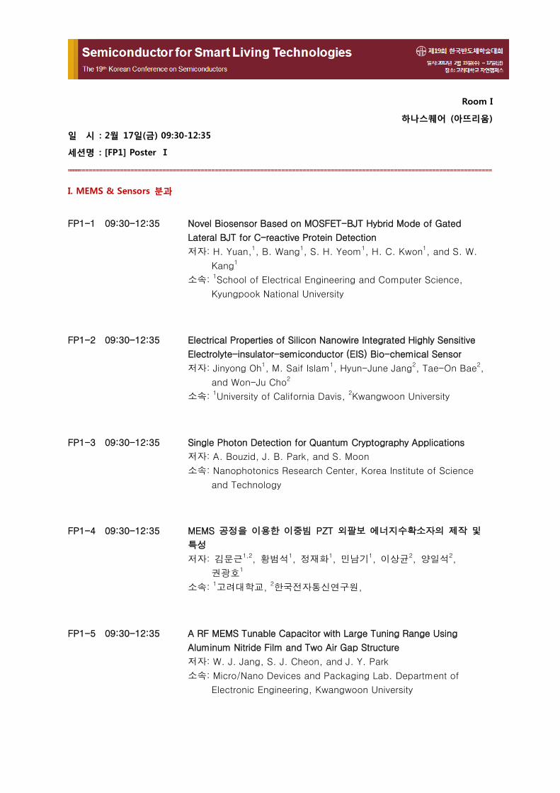
Room I
하나스퀘어 (아뜨리움)
일 시 : 2월 17일(금) 09:30-12:35
세션명 : [FP1] Poster Ⅰ
==========================================================================================================================
I. MEMS & Sensors 분과
FP1-1 09:30-12:35 Novel Biosensor Based on MOSFET-BJT Hybrid Mode of Gated
Lateral BJT for C-reactive Protein Detection
저자: H. Yuan,1, B. Wang1, S. H. Yeom1, H. C. Kwon1, and S. W.
Kang1
소속: 1School of Electrical Engineering and Computer Science,
Kyungpook National University
FP1-2 09:30-12:35 Electrical Properties of Silicon Nanowire Integrated Highly Sensitive
Electrolyte-insulator-semiconductor (EIS) Bio-chemical Sensor
저자: Jinyong Oh1, M. Saif Islam1, Hyun-June Jang2, Tae-On Bae2,
and Won-Ju Cho2
소속: 1University of California Davis, 2Kwangwoon University
FP1-3 09:30-12:35 Single Photon Detection for Quantum Cryptography Applications
저자: A. Bouzid, J. B. Park, and S. Moon
소속: Nanophotonics Research Center, Korea Institute of Science
and Technology
FP1-4 09:30-12:35 MEMS 공정을 이용한 이중빔 PZT 외팔보 에너지수확소자의 제작 및
특성
저자: 김문근1,2, 황범석1, 정재화1, 민남기1, 이상균2, 양일석2,
권광호1
소속: 1고려대학교, 2한국전자통신연구원,
FP1-5 09:30-12:35 A RF MEMS Tunable Capacitor with Large Tuning Range Using
Aluminum Nitride Film and Two Air Gap Structure
저자: W. J. Jang, S. J. Cheon, and J. Y. Park
소속: Micro/Nano Devices and Packaging Lab. Department of
Electronic Engineering, Kwangwoon University
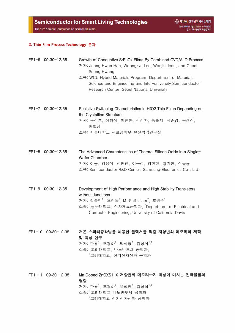
D. Thin Film Process Technology 분과
FP1-6 09:30-12:35 Growth of Conductive SrRuOx Films By Combined CVD/ALD Process
저자: Jeong Hwan Han, Woongkyu Lee, Woojin Jeon, and Cheol
Seong Hwang
소속: WCU Hybrid Materials Program, Department of Materials
Science and Engineering and Inter-university Semiconductor
Research Center, Seoul National University
FP1-7 09:30-12:35 Resistive Switching Characteristics in HfO2 Thin Films Depending on
the Crystalline Structure
저자: 윤정호, 정형석, 이민환, 김건환, 송슬지, 석준영, 윤경진,
황철성
소속: 서울대학교 재료공학부 유전박막연구실
FP1-8 09:30-12:35 The Advanced Characteristics of Thermal Silicon Oxide in a Single-
Wafer Chamber.
저자: 이웅, 김용석, 신현진, 이우성, 임헌형, 황기현, 신유균
소속: Semiconductor R&D Center, Samsung Electronics Co., Ltd.
FP1-9 09:30-12:35 Development of High Performance and High Stability Transistors
without Junctions
저자: 정승민1, 오진용2, M. Saif Islam2, 조원주1
소속: 1광운대학교, 전자재료공학과, 2Department of Electrical and
Computer Engineering, University of California Davis
FP1-10 09:30-12:35 저온 스퍼터증착법을 이용한 플렉서블 적층 저항변화 메모리의 제작
및 특성 연구
저자: 한용1, 조경아2, 박석형2, 김상식1,2
소속: 1고려대학교, 나노반도체 공학과, 2고려대학교, 전기전자전파 공학과
FP1-11 09:30-12:35 Mn Doped ZnOXS1-X 저항변화 메모리소자 특성에 미치는 전극물질의
영향
저자: 한용1, 조경아2, 윤정권2, 김상식1,2
소속: 1고려대학교 나노반도체 공학과, 2고려대학교 전기전자전파 공학과
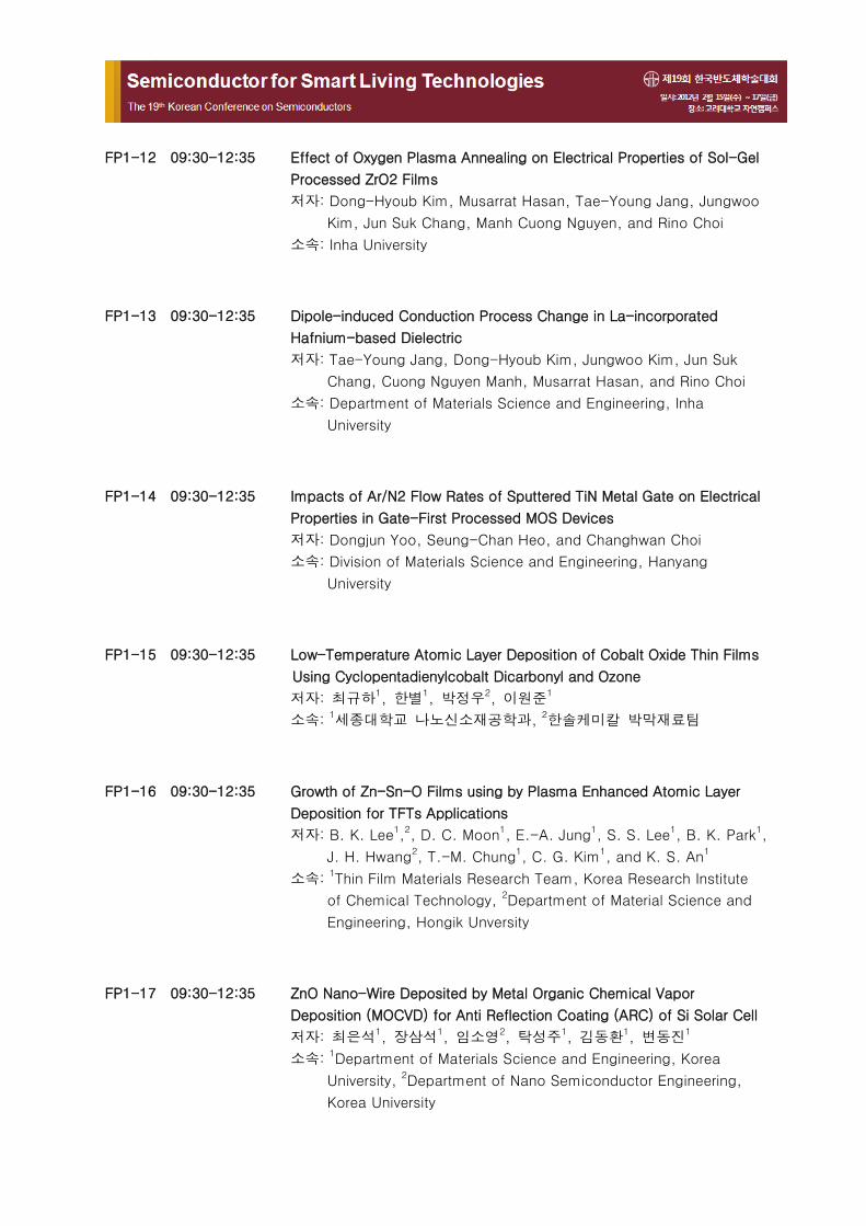
FP1-12 09:30-12:35 Effect of Oxygen Plasma Annealing on Electrical Properties of Sol-Gel
Processed ZrO2 Films
저자: Dong-Hyoub Kim, Musarrat Hasan, Tae-Young Jang, Jungwoo
Kim, Jun Suk Chang, Manh Cuong Nguyen, and Rino Choi
소속: Inha University
FP1-13 09:30-12:35 Dipole-induced Conduction Process Change in La-incorporated
Hafnium-based Dielectric
저자: Tae-Young Jang, Dong-Hyoub Kim, Jungwoo Kim, Jun Suk
Chang, Cuong Nguyen Manh, Musarrat Hasan, and Rino Choi
소속: Department of Materials Science and Engineering, Inha
University
FP1-14 09:30-12:35 Impacts of Ar/N2 Flow Rates of Sputtered TiN Metal Gate on Electrical
Properties in Gate-First Processed MOS Devices
저자: Dongjun Yoo, Seung-Chan Heo, and Changhwan Choi
소속: Division of Materials Science and Engineering, Hanyang
University
FP1-15 09:30-12:35 Low-Temperature Atomic Layer Deposition of Cobalt Oxide Thin Films
Using Cyclopentadienylcobalt Dicarbonyl and Ozone
저자: 최규하1, 한별1, 박정우2, 이원준1
소속: 1세종대학교 나노신소재공학과, 2한솔케미칼 박막재료팀
FP1-16 09:30-12:35 Growth of Zn-Sn-O Films using by Plasma Enhanced Atomic Layer
Deposition for TFTs Applications
저자: B. K. Lee1,2, D. C. Moon1, E.-A. Jung1, S. S. Lee1, B. K. Park1,
J. H. Hwang2, T.-M. Chung1, C. G. Kim1, and K. S. An1
소속: 1Thin Film Materials Research Team, Korea Research Institute
of Chemical Technology, 2Department of Material Science and
Engineering, Hongik Unversity
FP1-17 09:30-12:35 ZnO Nano-Wire Deposited by Metal Organic Chemical Vapor
Deposition (MOCVD) for Anti Reflection Coating (ARC) of Si Solar Cell
저자: 최은석1, 장삼석1, 임소영2, 탁성주1, 김동환1, 변동진1
소속: 1Department of Materials Science and Engineering, Korea
University, 2Department of Nano Semiconductor Engineering,
Korea University
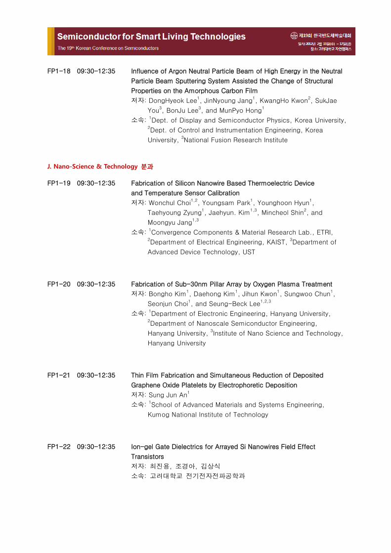
FP1-18 09:30-12:35 Influence of Argon Neutral Particle Beam of High Energy in the Neutral
Particle Beam Sputtering System Assisted the Change of Structural
Properties on the Amorphous Carbon Film
저자: DongHyeok Lee1, JinNyoung Jang1, KwangHo Kwon2, SukJae
You3, BonJu Lee3, and MunPyo Hong1
소속: 1Dept. of Display and Semiconductor Physics, Korea University, 2Dept. of Control and Instrumentation Engineering, Korea
University, 3National Fusion Research Institute
J. Nano-Science & Technology 분과
FP1-19 09:30-12:35 Fabrication of Silicon Nanowire Based Thermoelectric Device
and Temperature Sensor Calibration
저자: Wonchul Choi1,2, Youngsam Park1, Younghoon Hyun1,
Taehyoung Zyung1, Jaehyun. Kim1,3, Mincheol Shin2, and
Moongyu Jang1,3
소속: 1Convergence Components & Material Research Lab., ETRI, 2Department of Electrical Engineering, KAIST, 3Department of
Advanced Device Technology, UST
FP1-20 09:30-12:35 Fabrication of Sub-30nm Pillar Array by Oxygen Plasma Treatment
저자: Bongho Kim1, Daehong Kim1, Jihun Kwon1, Sungwoo Chun1,
Seonjun Choi1, and Seung-Beck Lee1,2,3
소속: 1Department of Electronic Engineering, Hanyang University, 2Department of Nanoscale Semiconductor Engineering,
Hanyang University, 3Institute of Nano Science and Technology,
Hanyang University
FP1-21 09:30-12:35 Thin Film Fabrication and Simultaneous Reduction of Deposited
Graphene Oxide Platelets by Electrophoretic Deposition
저자: Sung Jun An1
소속: 1School of Advanced Materials and Systems Engineering,
Kumog National Institute of Technology
FP1-22 09:30-12:35 Ion-gel Gate Dielectrics for Arrayed Si Nanowires Field Effect
Transistors
저자: 최진용, 조경아, 김상식
소속: 고려대학교 전기전자전파공학과
FP1-23 09:30-12:35 Fabrication of Beta-phase Poly(9,9-dioctylfluorene) Nanowire Array
using Direct Printing Method
저자: Jangmi Back and Myung M. Sung
소속: Department of Chemistry, HanyangUniversity
FP1-24 09:30-12:35 Graphene Sheets as p-type Transparent Conducting Electrodes in
GaN Light Emitting Diodes
저자: Jung Min Lee, Hae Yong Jeong, and Won Il Park
소속: Division of Materials Science and Engineering, Hanyang
University
FP1-25 09:30-12:35 Fabrication of Vapor Phase Polymerized PEDOT Nanowire Arrays
Using Liquid-Bridge-Mediated Nanotransfer Molding
저자: Boram Cho, Hyun S. Oh, and Myung M. Sung
소속: Department of Chemistry, Hanyang University
FP1-26 09:30-12:35 N-type Carbon Nanotube Network Device based on Tunneling through
SnO2
저자: Young Jun Heo, Jun Ho Cheon, Seok Ha Lee, Jaeheung Lim,
and Young June Park
소속: School of Electrical Engineering, Seoul National University
FP1-27 09:30-12:35 The Predicted Crystal Structure of Li4C6O6, an Organic Cathode
Material for Li-ion Batteries: First-principles Multi-scale
Computational Study
저자: Dong-Hwa Seo1, Hyungjun Kim2, Haegyeom Kim1, William A.
Goddard III2,3, and Kisuk Kang1
소속: 1Department of Materials Science and Engineeing, Seoul
National University, 2Graduate School of EEWS, KAIST, 3Materials and Process Simulation Center, California Institute of
Technology
FP1-28 09:30-12:35 Fabricated Various Metallic Nano-sized Pattern using Ag Ink Printing
Technique
저자: 오상철1, 신주현2, 김진승2, 김양두3, 이헌1,2,3
소속: 1고려대학교 나노반도체공학과, 2고려대학교 신소재공학과, 3고려대학교 바이오-마이크로 시스템 협동과정
FP1-29 09:30-12:35 A Graphene/Nanocluster Hybrid Nanomaterial-Based Gas Sensor
저자: I.-S. Kang and C. W. Ahn
소속: National Nanofab Center
FP1-30 09:30-12:35 Color Tunable OLEDs using Localized Surface Plasmons
저자: Illhwan Lee, Kihyon Hong, Sungjun Kim, and Jong-Lam Lee
소속: Department of Materials Science and Engineering and Division
of Advanced Materials Science, POSTECH
FP1-31 09:30-12:35 Analytic Model of Spin-Torque Oscillators(STO) for Circuit-Level
Simulation
저자: 안소라1, 임혜인1, 서수만2, 이경진2, 신형순1, 이승준1
소속: 1이화여자대학교 전자공학과, 2고려대학교 신소재공학과
FP1-32 09:30-12:35 Porosity Modulated Silicon Nanowires
저자: Jungkil Kim1,2 and Woo Lee1,2
소속: 1Korea Research Institute of Standards and Science, 2Department of Nano Science, University of Science and
Technology
N. VLSI CAD 분과
FP1-33 09:30-12:35 Thermal Modeling of 3D Stacked MLC NAND Flash Memory
저자: 김동기1, 유승주1, 이승구1
소속: 1포항공과대학교 전자전기공학과
FP1-34 09:30-12:35 System Model for CPU/GPU Architecture
저자: 이성광1, 유승주1, 정재웅2, 우동혁2, 김대현2
소속: 1포항공과대학교 전자전기공학과, 2Intel Corporation
FP1-35 09:30-12:35 High-Throughput Double-Binary MAP Decoder with Reduced Memory
Requirement
저자: 김지훈
소속: 충남대학교 전자공학과
FP1-36 09:30-12:35 Promoting Data Reuse on Shared Memory of Hybrid System
저자: Toan X. Mai, Yeonghun Jeong, Jongeun Lee
소속: School of Electrical and Computer Engineering, Ulsan National
Institute of Science and Technology
FP1-37 09:30-12:35 쓰기 데이터 특성 파악을 통한 Wear-Leveling
저자: 유태희, 박상훈, 서혁준, 정의영
소속: 연세대학교, 전기전자공학과
FP1-38 09:30-12:35 Interleaved Garbage Collection Scheme using Dynamic Channel/Way
Allocation for Solid-State Drive
저자: 김동건, 박상훈 서혁준, 정의영
소속: 연세대학교, 전기전자공학부
Q. Metrology, Inspection, and Yield Enhancement 분과
FP1-39 09:30-12:35 초음속 나노입자빔을 이용한 실리콘 웨이퍼 표면오염입자(10nm) 제거
실험
저자: 김인호, 이진원
소속: 포항공과대학교 기계공학과
FP1-40 09:30-12:35 Characterization of Overlay Error Induced by Film Stress Using Local
Stress Monitoring Tool
저자: C. H. Lee1, J. T. Kim1, J. H. Kim1, H. Y. Yoo1, I. K. Han1, and
W. S. Yoo2
소속: 1Hynix Semiconductor Inc., 2WaferMasters, Inc.
FP1-41 09:30-12:35 The Pattern Wiggling CD Metrology Using Flexible Scan & Dense
Function
저자: 김종태1, 이창환1, 유형원1, 한일근1, 고경보2, 곽동수3
소속: 1하이닉스 반도체 MI팀, 2하이닉스 반도체 DRAM공정AP팀, 3Hitachi High-Technologies
FP1-42 09:30-12:35 Electron Beam Inspection of Cell Mat Edge Using Image Averaging
and Comparison Method
저자: G. Kwon1, J. H. Oh1, D. Y. Mun1, H. W. Yoo1, J. C. Jo2, J. S.
Koo2, M. Nozoe2, T. Ninomiya2, T. Hiroi2, and H. Okuda2
소속: 1Hynix Semiconductor Inc., 2Central Research Laboratory,
Hitachi High-Technologies
FP1-43 09:30-12:35 The Measurement of OCD (Optical critical dimension) for Yield
Enhancement at Edge Die
저자: Seok Park, Won Sik Yun, Chang Hwan Lee, Sung Su Kim,
Hyung Won Yoo, and Il Keoun Han
소속: Hynix Semiconductor Inc.
FP1-44 09:30-12:35 The MASK CD Control (CDC) Using OCD Applications
저자: Hyun Chul Shin, Seok Park, Won Sik Yun, Chang Hwan Lee,
Hyung Won Yoo, and Il Keoun Han
소속: Hynix Semiconductor Inc.
FP1-45 09:30-12:35 The In-Line Monitoring Method of ZAZ Thickness Using WD-XRF
저자: Jun Soo Kim, Sang Hoon Son, Shin Wang Ju, Hyung Won Yoo,
and Il Keoun Han
소속: Hynix Semiconductor Inc.
FP1-46 09:30-12:35 Substrate Materials Dependent Growth Characteristics of the Initial
Stage of ALD Ruthenium Films Using Synchrotron Radiation X-ray
Scattering.
저자: Y. J. Park1 and D. R. Lee2
소속: 1Pohang Accelerator Laboratory, Pohang University of Science
and Technology, 2Department of Physics, Soongsil University
FP1-47 09:30-12:35 Improvement of Measurement Resolution for Determining Geometrical
Thickness of a Silicon Wafer using a Femtosecond Pulse Laser
저자: 맹새롬1,3, 박정재1, 진종한1,2, 김재완1,2, 강주식1,2, 김종안1,
오병성3
소속: 1한국표준과학연구원 길이센터, 2과학기술연합대학원대학교, 3충남대학교 물리학과
FP1-48 09:30-12:35 다결정성텅스텐 나노팁의 저전압 전계방출 안정성 평가
저자: 정재은, 안상정, 박창준, 김주황, 송운, 김달현, 배문섭, 이확주,
조양구
소속: 한국표준과학연구원 나노이미징기술센터
Room I
하나스퀘어 (아뜨리움)
일 시 : 2월 17일(금) 13:40-16:45
세션명 : [FP2] Poster Ⅱ
==========================================================================================================================
B. Patterning 분과
FP2-1 13:40-16:45 Hydrogen Plasma Characteristics by Cylindrical Inductively Coupled
Plasma for Photoresist Strip Process
저자: 양승국, 강정현, 조주형, 이성욱, 조정희, 채희선
소속: 피에스케이㈜ 연구소
FP2-2 13:40-16:45 AlGaInP기반 LED에서 공기 층 Hybrid DBR구조 삽입을 통한 발광 효율
향상에 관한 연구
저자: 류호성1,2, 박준모1,3, 백종협1, 곽준섭2, 오화섭1
소속: 1 한국광기술원 LED소자연구센터, 2순천대학교 WCU인쇄전자공
학과, 3전남대학교 물리학과
FP2-3 13:40-16:45 Investigation on Etch Characteristics of Magnetic Tunnel Junction
Stacks in a CH4/O2/Ar Plasma
저자: Tea Young Lee, Eun Ho Kim, and Chee Won Chung
소속: Department of Chemical Engineering, Inha University
FP2-4 13:40-16:45 Inductively Coupled Plasma Reactive Ion Etching of MgO Thin Films in
CH4/Ar Plasma
저자: Tea Young Lee. Eun Ho Kim, Il Hoon Lee, and Chee Won
Chung
소속: Department of Chemical Engineering, Inha University
FP2-5 13:40-16:45 용매 증발 제어를 통한 고분자 복합 소재의 Non-Lithography 패터닝
기술
저자: 정희준, 박철민
소속: 연세대학교 신소재과학과
FP2-6 13:40-16:45 Inductively Coupled Plasma Effect on Graphene Field Effect Transistor
저자: Y. D. Lim, D. Y. Lee, and W. J. Yoo
소속: Department of Nano Science and Technology, Sungkyunkwan
University
E. Compound Semiconductors 분과
FP2-7 13:40-16:45 Influence of Series Resistance and Interface State Density on
Electrical Characteristics of Ru/Ni/n-GaN Schottky diode
저자: M. Siva Pratap Reddy1, V. Rajagopal Reddy2, and Jung-Hee
Lee1
소속: 1School of Electrical Engineering, Kyungpook National
University, 2Department of Physics, Sri Venkateswara Univeristy
FP2-8 13:40-16:45 Drain Field Plate를 통한 AlGaN/GaN HEMT의 Off-state Breakdown
Voltage 특성 개선에 관한 연구
저자: 안호정1, 최우진1, 박봉렬2, 차호영2, 서광석1
소속: 1서울대학교, 전기컴퓨터공학, 2홍익대학교, 전자전기공학
FP2-9 13:40-16:45 Sapphire Substrate 밑면에 성장시킨 ZnO Nanorods의 LED성능에 미
치는 영향
저자: 진주, 류버들, 한민, 김현규, 김희윤, 박재영, 홍창희
소속: 전북대학교 반도체 화학공학부
FP2-10 13:40-16:45 BCl3 ICP 건식 식각 공정으로 게이트 리세스한 0.25um T-gate
AlGaN/GaN/SiC HEMT 소자제작 및 특성
저자: 송인협1,2, 장경욱1, 안호균2, 민병규2, 임종원2, 강동민2, 김성일2,
장우진2, 이종민2, 윤형섭2, 문재경2
소속: 1한서대학교 신소재공학과, 2한국전자통신연구원 RF융합부품연구팀
FP2-11 13:40-16:45 Deep Level Defects in InGaN/GaN Blue Light Emitting Diode
저자: P. Koteswara Rao1, Byungguon Park1, Sang-Tae Lee1, Moon-
Deock, Kim1, Jae-Eung Oh2, and Song-Gang Kim3
소속: 1Department of Physics, Chungnam National University, 2School of Electrical and Computer Engineering, Hanyang
University, 3Department of Information and Communications,
Joongbu University
FP2-12 13:40-16:45 Effect of Gate Leakage Current on AlGaN/GaN HEMTs with Electron
Beam Irradiation
저자: Seung Kyu Oh, S. M. Wie, and Joon Seop Kwak
소속: Department of Printed Electronics Engineering, Sunchon
National University
FP2-13 13:40-16:45 LED Light Extraction Efficiency Study of GaN based Light Emitting
Diodes using by Various ion Implanted Current Blocking Layer
저자: Y. D. Kim, M. J. Park, and J. S. Kwak
소속: Department of Printed Electronics Engineering, Sunchon
National University
C. Materials Growth & Characterization 분과
FP2-14 13:40-16:45 Photoluminescence and Dielectric Function of Cuprous Oxide Thin
Films
저자: Jun-Woo Park1, Hyungkeun Jang1, Sung Kim1, Suk-Ho Choi1,
Joongoo Kang2, Su-Huai Wei2, and Hosun Lee1
소속: 1Department of Applied Physics, Kyung Hee University, 2National Renewable Energy Laboratory
FP2-15 13:40-16:45 Homoepitaxial Growth of 4H-SiC on Carbon-Face Substrate Using
BTMSM
저자: Hun Hee Lee1,a, Han Seok Seo1, Jeong Hyuk Yim1, Do Hyun
Lee1, Changhyun Kim1, and Hyeong Joon Kim1
소속: 1Department of Materials Science and Engineering, Seoul
National University
FP2-16 13:40-16:45 Structural Properties of Nonpolar A-Plane MgxZn1-xO Films on R-
Plane Sapphire Substrates by Plasma-Assisted Molecular Beam
Epitaxy
저자: S. K. Han1, H. S. Lee1, D. S. Lim2, S. K. Hong1,2, M. H. Sung3,
J. Y. Lee3, and T. Yao4
소속: 1Department of Advanced Materials Engineering, Chungnam
National University, 2Graduate School of Green Energy
Technology, Chungnam National University, 3Department of
Materials Science and Engineering, KAIST, 4Center for
Interdisciplinary Research, Tohoku
FP2-17 13:40-16:45 Influence of Temperature on Structural, Optical Properties and
Chemical Bonding Energy of TiO2 Thin Film Grown on Glass Substrate
by PLD
저자: 빈민욱1, 이원재1, 최은호2, 유영조2
소속: 1동의대학교 융합부품공학과, 2삼성코닝정밀소재 에너지 소재 Lab
FP2-18 13:40-16:45 Ni-Assisted, Large-Area Graphene Growth using Rapid Thermal
Annealing
저자: Jae Hwan Chu1, Jinsung Kwak1, Tae-Yang Kwon, Soon-Dong
Park1, Heungseok Go2, Sing Youb Kim1, Kibog Park2, and
Soon-Yong Kwon1
소속: 1School of Mechanical and Advanced Materials Engineering,
Ulsan National Institute of Science and Technology, 2School of
Electrical and Computer Engineering, Ulsan National Institute of
Science and Technology
FP2-19 13:40-16:45 2-Step ELOG of GaN on C-plane Sapphire using Carbonized PR Mask
저자: Sungwook Moon1, Sang-il Kim2, Samseok Jang2, Jungyeop
Hong1, Junhyuck Kwon2, and Dongjin Byun1,2
소속: 1Department of Nano-photonics, Korea University, 2Department of Material Science and engineering, Korea
University
FP2-20 13:40-16:45 Improved Crystalline Quality of Si-doped A-plane GaN using Higher
Initial Growth Pressure
저자: Keun Man Song1, Jong Min Kim1, Chan Soo Shin1, Chul Gi Ko1,
Hyun Koun Cho2, Dae Ho Yoon2, Sung Min Hwang3, and
Hogyoung Kim4
소속: 1Korea Advanced Nano Fab Center, 2 School of Advanced
Materials Science and Engineering, Sungkyunkwan University, 3Korea Electronics Technology Institute, 4College of Humanities
and Sciences
FP2-21 13:40-16:45 Nucleation and Growth of GaN Compound on Various Powders
저자: 홍성기1, 이효종1, 박진섭2, 조명환3, Takafumi Yao3
소속: 1Materials Science and Engineering, Dong-A University, 2Department of Electronic Engineering, Hanyang University, 3Institute for Materials Research, Tohoku University
FP2-22 13:40-16:45 Growth of GaN Using Patterned Metal Mask by Metal-organic
Chemical Vapor Deposition
저자: J. Park1, D. Moon2, S. Park2, S. H. Park2, and E. Yoon2
소속: 1Department of Electronic Engineering, Hanyang University, 2Department of Materials Science and Engineering, College of
Engineering, Seoul National University
FP2-23 13:40-16:45 Growth of Monolayer Graphene from Solid Carbon Source Using Rapid
Thermal Annealing
저자: J. Kwak1, J.H. Chu1, T.-Y. Kwon1, S.-D. Park1, S.Y. Kim1, K.
Park2, and S.-Y. Kwon1,2
소속: 1School of Mechanical and Advanced Materials Engineering,
Ulsan National Institute of Science and Technology, 2School of
Electrical and Computer Engineering, Ulsan National Institute of
Science and Technology
FP2-24 13:40-16:45 Investigation of Crystallization Procedurs and Crystal Structures of
Nitrogen Doped GeSb Phase Change Film
저자: Hyung Keun Kim and Doo jin Choi
소속: Department of Material Science and Engineering, Yonsei
University
FP2-25 13:40-16:45 Fabrication of Vertically Aligned GaN/air-gap Microstructures using
Doping Selective Electrochemical Etching
저자: Ah Hyun Park, Yong Seok Lee, Hyun Jeong, Tae Hoon Seo,
Kang Jea Lee, and Eun Kyung Suh
소속: Semiconductor Physics Research Center,
Chonbuk National University
FP2-26 13:40-16:45 Structural and Electrical Properties of Nano-Crystalline Graphite Layer
on 6H-SiC Formed by Direct Electron Beam Irradiation
저자: Heung Seok Go1, Jinsung Kwak2, Youngeun Jeon1, Bum-Kyu
Kim3, Nam Kim4, Jae-Hyun Ko5, Sung Youb Kim2, Byung Cheol
Lee6, Hyun Suk Kang6, Soon-Yong Kwon2, and Kibog Park1
소속: 1Electrical and Computer Engineering, Ulsan 1National Institute
of Science and Technology, 2Mechanical and Advanced
Materials Engineering, Ulsan National Institute of Science and
Technology, 3Physics, Chonbuk National University, 4Division of
Convergence
FP2-27 13:40-16:45 Growth of InP/InGaP Quantum Structure for the 808-nm Wavelength
Emission
저자: S.Y. Kim1,2, E.H. Lee1, J. D. Song1, I. K. Han1, J. I. Lee1, and
T. W. Kim2
소속: 1Nano Photonics Research Center, Korea institute of Science
and Technology, 2Division of Electronics and Computer
Engineering, Hanyang University
FP2-28 13:40-16:45 Molecular Beam Epitaxy를 이용한 Large Droplet Island 성장
저자: 이은혜1, 송진동1,2, 김수연1, 배민환1, 한일기1, 장수경2,
이정일1
소속: 1한국과학기술연구원 나노포토닉스센터, 2연세대학교 물리학과
FP2-29 13:40-16:45 Enhancement of Emission from InGaN/GaN Multiple Quantum Wells
via Surface Plasmon Resonance
저자: Kyoung Su Lee, Seon Pil Kim, and Eun Kyu Kim
소속: Quantum-Function Research Lab. and Department of Physics,
Hanyang University
K. Memory (Design & Process Technology) 분과
FP2-30 13:40-16:45 A Novel Cross-Bar Array Scheme to Suppress Sneak Path Current in
Memory Operation
저자: Jun Yeong Seok, Gun Hwan Kim, Seul Ji Song, Jung Ho Yoon,
Kyung Jin Yoon, Min Hwan Lee, and Cheol Seong Hwang
소속: WCU Hybrid Materials Program, Department of Materials
Science and Engineering and Inter-university Semiconductor
Research Center, Seoul National University
FP2-31 13:40-16:45 ZrN기반의 저항 변화 메모리의 스위칭 메커니즘 및 기억유지 특성 연
구
저자: 김희동, 안호명, 서유정, 김경헌, 송민영, 이동명, 김태근
소속: 고려대학교 전기전자전파공학과
FP2-32 13:40-16:45 Bipolar Switching Behavior of ZnO Thin Films Deposited by Metal
Organic Chemical Vapor Deposition using Different Growth
Temperature
저자: So Young Yim1, Jong-Han Lee2, Samseok Jang2, Do Han Lee2,
Tae-Geun Seong1, Sahm Nahm1,2, Dongjin Byun2
소속: 1Department of Nano Semiconductor Engineering, Korea
university, 2Department of Materials Science and Engineering,
Korea university
FP2-33 13:40-16:45 Ion Beam Etching of Sub-30nm Scale Perpendicular-MTJ for
Reducing by-Product and Damage of Sidewall.
저자: Daehong Kim1, Bongho Kim1, Sungwoo Chun1, Jihun Kwon1,
Seonjun Choi1, and Seung-Beck Lee1,2
소속: 1Department of Electronic Engineering, Hanyang University, 2Institute of Nano Science and Technology, Hanyang University
FP2-34 13:40-16:45 Resistive Switching Properties of TaOx with a Variety of Reactive Metal
저자: 송성호1, 양민규1, 김재혁1, 성동준1, 주현수1, 김은미1, 박찬진1,
박성건1, 백인규1, 박순오1, 최시영1
소속: 1삼성전자 반도체연구소 공정개발팀
FP2-35 13:40-16:45 Si/SiGe Vertical Gate DHBT (VerDHBT)-based 1T DRAM Cell for
Improved Retention Characteristics with a Large Hysteresis Window
저자: Ja Sun Shin, Hyunjun Choi, Hagyoul Bae, Jaeman Jang,
Daeyoun Yun, Euiyoun Hong, Hyojoon Seo, Dae Hwan Kim,
and Dong Myong Kim
소속: School of Electrical Engineering, Kookmin University
FP2-36 13:40-16:45 Deposition Temperature Dependence of the Memory Characteristics
for AYO(Al2O3/Y2O3/SiO2) Multi-Stacked Film
저자: Hye Young Jung1,2 and Doo Jin Choi1
소속: 1Department of Materials Science & Engineering, Yonsei
University, 2Samsung Electronics co., Ltd.
G. Device & Process Modeling, Simulation and Reliability 분과
FP2-37 13:40-16:45 Optical Modeling of NBIS Instability and Hole Current in a-IGZO
Systems
저자: Yoon Jang Chung1, Un Ki Kim1, Jeong Hwan Kim1, Eric
Hwang1, Sang ho Rha2, and Cheol Seong Hwang1
소속: 1WCU Hybrid Materials Program, Department of Materials
Science and Engineering and Inter-university Semiconductor
Research Center, Seoul National University, 2Department of
Nano Science and Technology, Graduate School of
Convergence Science and Technology
FP2-38 13:40-16:45 A Smart Scribe SRAM Test Structure for Bitcell Variation
Characterization in Macro Level
저자: 김현수, 김형태, 황재철, 김영현, 배윤미, 윤성준, 이은철,
홍규식
소속: 삼성전자 System LSI, Product & Test Engineering Team
FP2-39 13:40-16:45 A Product Representative Scribe-Line Process Monitor for CMOS
Analog/Mixed-Signal Circuit Performance Characterizaiton and Yield
Improvement
저자: 김형태, 김현수, 김영현, 황재철, 배윤미, 윤성준, 이은철,
홍규식
소속: 삼성전자 System LSI 제품기술팀
FP2-40 13:40-16:45 Simulation Study of Resurf Stepped Oxide (RSO) Type Semi Super-
Junction (semi-SJ) Trench Double Diffusion MOSFET (TDMOS) with
Various Geometrical Parameters
저자: 나경일, 구진근, 김상기, 김종대, 양일석, 이진호
소속: 한국전자통신연구원, 융합부품소재연구부분
FP2-41 13:40-16:45 Dynamic Pixel Test Pattern for CMOS Image Sensor
저자: KS Lee, HJ Lee, MJ Jang, JC Kim, ST Kim, JW Moon, IW Cho,
and KD Yoo
소속: Hynix Semiconductor Inc.
FP2-42 13:40-16:45 Separate Extraction Technique of Gate, Source, Drain, and Substrate
Resistances in Individual MOSFET Combining I-V and C-V
Characteristics
저자: Ja Sun Shin, Hagyoul Bae, Euiyoun Hong, Jaeman Jang,
Daeyoun Yun, Hyojoon Seo, Hyunjun Choi, Dae Hwan Kim, and
Dong Myong Kim
소속: School of Electrical Engineering, Kookmin University
FP2-43 13:40-16:45 Migration of Oxygen Ions and Vacancies in Tunneling based
Resistance Switching Element
저자: Seung Jae Baik
소속: Department of Electrical Engineering, KAIST
FP2-44 13:40-16:45 Design Optimization of Vertical Double Gate SiGe/Si Heterostucture
Tunneling Field-Effect Transistors
저자: 윤영준1, 이재성2, 박윤수2, 서재화3, 우성윤1, 강인만1
소속: 1경북대학교 전자공학부, 2경북대학교 전자전기컴퓨터학부
FP2-45 13:40-16:45 Measurement of Band Bending Voltage in SiO2/poly-Silicon Stack
during FN Tunneling by Constant Current Stress Test
저자: 나희도, 오진호, 목인수, 김종기, 이규민, 이성훈, 손현철
소속: 연세대학교 신소재공학과
FP2-46 13:40-16:45 Accuracy Verification of Asymmetric Substrate Resistance Model for
Multi-Finger RF MOSFETs
저자: Min-Kwon Choi, Ju-Young Kim, and Seonghearn Lee
소속: Department of Electronic Engineering, Hankuk University of
Foreign Studies
FP2-47 13:40-16:45 Analytical Model-Based SPICE Simulation for the Design of
Amorphous InGaZnO Thin-Film Transistors-Based Circuits
저자: 김우준, 배민경, 김용식, 김재형, 허인석, 장재만, 정현광,
공동식, 김윤혁, 이재욱, 조춘형, 전성우, 김동명, 김대환
소속: School of Electrical Engineering, Kookmin University