ltc3412 2.5a, 4mhz, monolithic synchronous step-down regulator
TRANSCRIPT
LTC3412
13412fc
For more information www.linear.com/LTC3412
TYPICAL APPLICATION
FEATURES DESCRIPTION
2.5A, 4MHz, MonolithicSynchronous Step-Down Regulator
The LTC®3412 is a high efficiency monolithic synchro-nous, step-down DC/DC converter utilizing a constant frequency, current mode architecture. It operates from an input voltage range of 2.625V to 5.5V and provides an adjustable regulated output voltage from 0.8V to 5V while delivering up to 2.5A of output current. The inter-nal synchronous power switch with 85mΩ on-resistance increases efficiency and eliminates the need for an external Schottky diode. Switching frequency is set by an external resistor or can be sychronized to an external clock. 100% duty cycle provides low dropout operation extending bat-tery life in portable systems. OPTI-LOOP® compensation allows the transient response to be optimized over a wide range of loads and output capacitors.
The LTC3412 can be configured for either Burst Mode® operation or forced continuous operation. Forced con-tinuous operation reduces noise and RF interference while Burst Mode operation provides high efficiency by reducing gate charge losses at light loads. In Burst Mode operation, external control of the burst clamp level allows the output voltage ripple to be adjusted according to the requirements of the application. To further maximize bat-tery life, the P-channel MOSFET is turned on continuously in dropout (100% duty cycle).
APPLICATIONS
■ High Efficiency: Up to 95%■ 2.5A Output Current■ Low Quiescent Current: 62µA■ Low RDS(ON) Internal Switches: 85mΩ■ Programmable Frequency: 300kHz to 4MHz■ No Schottky Diode Required■ ±2% Output Voltage Accuracy■ 0.8V Reference Allows Low Output Voltage■ Selectable Forced Continuous/Burst Mode Operation
with Adjustable Burst Clamp■ Synchronizable Switching Frequency■ Low Dropout Operation: 100% Duty Cycle■ Power Good Output Voltage Monitor■ Overtemperature Protection■ Available in 16-Lead Thermally Enhanced TSSOP
and QFN Packages
■ Portable Instruments■ Battery-Powered Equipment■ Notebook Computers■ Distributed Power Systems■ Cellular Telephones■ Digital Cameras
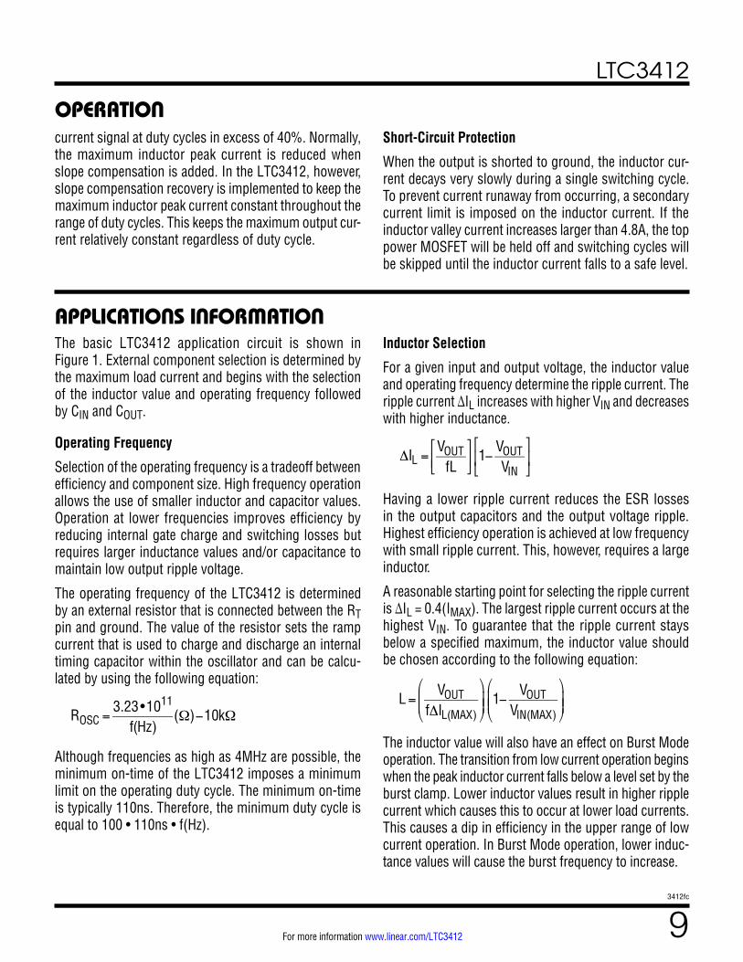
SVIN PVIN
PGOOD
SWLTC3412
PGND
SGNDRUN/SS
309k
VIN2.7V TO 5.5V
1000pF
RT
ITHVFBSYNC/MODE
1µH4.7M
470pF
75k
100pF
100µF
VOUT2.5V2.5A
15k
110k 392k
22µF
3412 F01
Figure 1. 2.5V, 2.5A Step-Down Regulator
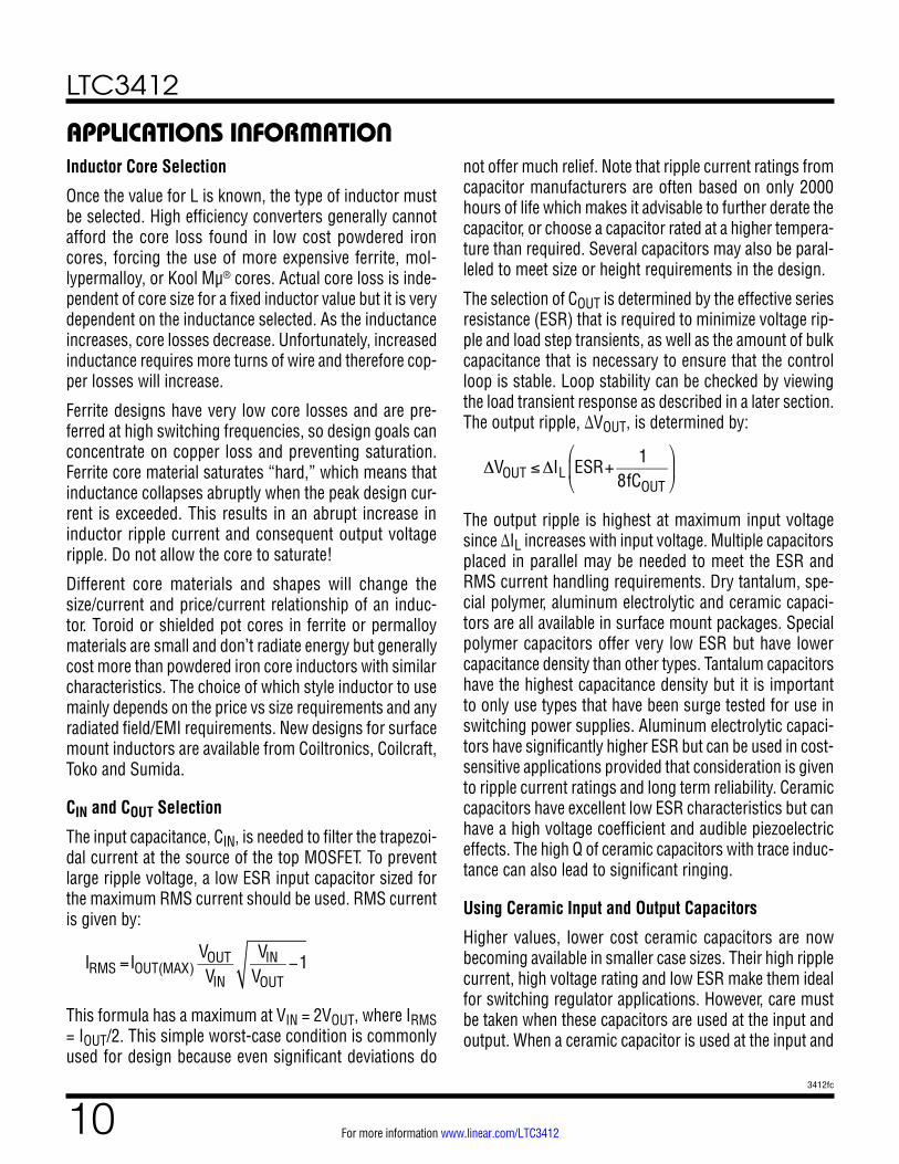
Efficiency vs Load Current
LOAD CURRENT (A)0.001
EFFI
CIEN
CY (%
)
100
80
60
40
20
010
3412 G01
VIN = 3.3VVOUT = 2.5V
Burst Mode OPERATION
FORCED CONTINUOUS
0.1 10.01
L, LT, LTC, LTM, Burst Mode, OPTI-LOOP, Linear Technology and the Linear logo are registered trademarks and ThinSOT is a trademark of Analog Devices, Inc. All other trademarks are the property of their respective owners.
LTC3412
23412fc
For more information www.linear.com/LTC3412
PIN CONFIGURATION
ABSOLUTE MAXIMUM RATINGS
Input Supply Voltage ....................................–0.3V to 6VITH, RUN, VFB Voltages ............................... –0.3V to VINSYNC/MODE Voltages ................................. –0.3V to VINSW Voltage ................................... –0.3V to (VIN + 0.3V)Peak SW Sink and Source Current ..........................6.5A
(Note 1)
1
2
3
4
5
6
7
8
TOP VIEW
FE PACKAGE16-LEAD PLASTIC TSSOP
16
15
14
13
12
11
10
9
SVIN
PGOOD
ITH
VFB
RT
SYNC/MODE
RUN/SS
SGND
PVIN
SW
SW
PGND
PGND
SW
SW
PVIN
17
EXPOSED PAD (PIN 17) IS SGND, MUST BE SOLDERED TO PCB
TJMAX = 125°C, θJA = 37.6°C/W, θJC = 10°C/W
16 15 14 13
5 6 7 8
TOP VIEW
17
UF PACKAGE16-LEAD (4mm × 4mm) PLASTIC QFN
9
10
11
12
4
3
2
1RUN/SS
SGND
PVIN
SW
PGOOD
SVIN
PVIN
SW
SYNC
/MOD
E
R T V FB
I TH
SW
PGND
PGND SW
EXPOSED PAD (PIN 17) IS SGND, MUST BE SOLDERED TO PCB
TJMAX = 125°C, θJA = 34°C/W, θJC = 1°C/W
ORDER INFORMATION http://www.linear.com/product/LTC3412#orderinfo
LEAD FREE FINISH TAPE AND REEL PART MARKING* PACKAGE DESCRIPTION TEMPERATURE RANGE
LTC3412EFE#PBF LTC3412EFE#TRPBF 3412EFE 16-Lead Plastic TSSOP –40°C to 125°C
LTC3412IFE#PBF LTC3412IFE#TRPBF 3412IFE 16-Lead Plastic TSSOP –40°C to 125°C
LTC3412EUF#PBF LTC3412EUF#TRPBF 3412 16-Lead (4mm × 4mm) Plastic QFN –40°C to 125°C
LEAD BASED FINISH TAPE AND REEL PART MARKING* PACKAGE DESCRIPTION TEMPERATURE RANGE
LTC3412EFE LTC3412EFE#TR 3412EFE 16-Lead Plastic TSSOP –40°C to 125°C
LTC3412IFE LTC3412IFE#TR 3412IFE 16-Lead Plastic TSSOP –40°C to 125°C
LTC3412EUF LTC3412EUF#TR 3412 16-Lead (4mm × 4mm) Plastic QFN –40°C to 125°C
Consult LTC Marketing for parts specified with wider operating temperature ranges. *The temperature grade is identified by a label on the shipping container.For more information on lead free part marking, go to: http://www.linear.com/leadfree/ For more information on tape and reel specifications, go to: http://www.linear.com/tapeandreel/. Some packages are available in 500 unit reels through designated sales channels with #TRMPBF suffix.
Operating Temperature Range (Note 2)....–40°C to 85°CStorage Temperature Range .................. –65°C to 150°CJunction Temperature (Note 5) ............................. 125°CLead Temperature (Soldering, 10 sec) TSSOP ...... 300°C
LTC3412
33412fc
For more information www.linear.com/LTC3412
ELECTRICAL CHARACTERISTICS
Note 1: Stresses beyond those listed under Absolute Maximum Ratings may cause permanent damage to the device. Exposure to any Absolute Maximum Rating condition for extended periods may affect device reliability and lifetime.Note 2: The LTC3412E is guaranteed to meet performance specifications from 0°C to 85°C. Specifications over the –40°C to 85°C operating temperature range are assured by design, characterization and correlation with statistical process controls. The LTC3412I is guaranteed to meet specified performance over the –40°C to 85°C temperature range.
SYMBOL PARAMETER CONDITIONS MIN TYP MAX UNITS
SVIN Signal Input Voltage Range 2.625 5.5 V
VFB Regulated Feedback Voltage (Note 3) l 0.784 0.800 0.816 V
IFB Voltage Feedback Leakage Current 0.1 0.4 µA
∆VFB Reference Voltage Line Regulation VIN = 2.7V to 5.5V (Note 3) l 0.04 0.2 %V
VLOADREG Output Voltage Load Regulation Measured in Servo Loop, VITH = 0.36V Measured in Servo Loop, VITH = 0.84V
l
l
0.02 –0.02
0.2 –0.2
% %
∆VPGOOD Power Good Range ±7.5 ±9 %
RPGOOD Power Good Pull-Down Resistance 120 200 Ω
IQ Input DC Bias Current Active Current Sleep Shutdown
(Note 4) VFB = 0.78V, VITH = 1V VFB = 1V, VITH = 0V VRUN = 0V, VMODE = 0V
250 62
0.02
330 80 1
µA µA µA
fOSC Switching Frequency Switching Frequency Range
ROSC = 309kΩ (Note 6)
0.88 0.3
0.95 1.1 4
MHz MHz
fSYNC SYNC Capture Range (Note 6) 0.3 4 MHz
RPFET RDS(ON) of P-Channel FET ISW = 1A (Note 7) 85 110 mΩ
RNFET RDS(ON) of N-Channel FET ISW = –1A (Note 7) 65 90 mΩ
ILIMIT Peak Current Limit 4 5.4 A
VUVLO Undervoltage Lockout Threshold 2.375 2.500 2.625 V
ILSW SW Leakage Current VRUN = 0V, VIN = 5.5V 0.1 1 µA
VRUN RUN Threshold 0.5 0.65 0.8 V
IRUN RUN/SS Leakage Current 1 µA
The ● denotes the specifications which apply over the full operating temperature range, otherwise specifications are at TA = 25°C. VIN = 3.3V unless otherwise specified.
Note 3: The LTC3412 is tested in a feedback loop that adjusts VFB to achieve a specified error amplifier output voltage (ITH).Note 4: Dynamic supply current is higher due to the internal gate charge being delivered at the switching frequency.Note 5: TJ is calculated from the ambient temperature TA and power dissipation as follows: LTC3412: TJ = TA + PD (37.6°C/W).Note 6: 4MHz operation is guaranteed by design and not production tested.Note 7: Switch on resistance is guaranteed by design and test correlation in the UF package and by production test in the FE package.
LTC3412
43412fc
For more information www.linear.com/LTC3412
TYPICAL PERFORMANCE CHARACTERISTICS
Efficiency vs Load CurrentEfficiency vs Load Current Efficiency vs Load Current
LOAD CURRENT (A)0.001
EFFI
CIEN
CY (%
)
100
80
60
40
20
010
3412 G01
VIN = 3.3VVOUT = 2.5V
Burst Mode OPERATION
FORCED CONTINUOUS
0.1 10.01
100
90
80
70
60
50
40
30
20
10
0
LOAD CURRENT (A)0.001
EFFI
CIEN
CY (%
)
10
3412 G02
VOUT = 2.5V1MHzBurst Mode OPERATION
0.1 10.01
VIN = 3.3V VIN = 5V
LOAD CURRENT (A)0.001
EFFI
CIEN
CY (%
)
100
90
80
70
60
50
40
30
20
10
010
3412 G03
VOUT = 2.5V1MHzFORCED CONTINUOUS
0.1 10.01
VIN = 3.3V VIN = 5V
Efficiency vs FrequencyEfficiency vs Input Voltage Load Regulation
Load Step Transient Forced ContinuousBurst Mode Operation
Load Step Transient Burst Mode Operation
INPUT VOLTAGE (V)2.55 3.05 3.55 4.05 4.55 5.05
EFFI
CIEN
CY (%
)
98
96
94
92
90
88
86
3412 G04
VOUT = 2.5V1MHzBurst Mode OPERATION
LOAD = 100mA
LOAD = 1A
LOAD = 2.5A
FREQUENCY (kHz)300 800 1300 1800 2300 2800 3300 3800
EFFI
CIEN
CY (%
)
97
96
95
94
93
92
91
3412 G05
VIN = 3.3VVOUT = 2.5VLOAD = 1ABurst Mode OPERATION
1µH
0.47µH
2.2µH
LOAD CURRENT (A)0 0.5 1 1.5 2 2.5
%V O
UT/V
OUT
0.02
0.00
–0.02
–0.04
–0.06
–0.08
–0.10
–0.12
–0.14
–0.16
–0.18
3412 G06
VIN = 3.3VVOUT = 2.5V
4µs/DIV
V OUT
20m
V/DI
VI L
200m
A/DI
V
3412 G07 20µs/DIV 3412 G08
V OUT
100m
V/DI
VI L
1A/D
IV
20µs/DIV 3412 G09
V OUT
100m
V/DI
VI L
1A/D
IV
LTC3412
53412fc
For more information www.linear.com/LTC3412
TYPICAL PERFORMANCE CHARACTERISTICS
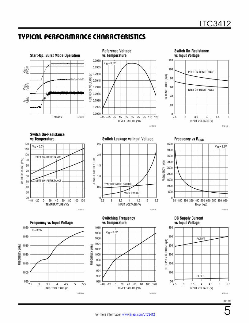
Start-Up, Burst Mode OperationReference Voltage vs Temperature
Switch On-Resistance vs Input Voltage
Switch On-Resistance vs Temperature Switch Leakage vs Input Voltage Frequency vs ROSC
Frequency vs Input VoltageSwitching Frequency vs Temperature
DC Supply Current vs Input Voltage
1ms/DIV 3412 G10
V OUT
1V/D
IVV R
UN1V
/DIV
I L1A
/DIV
TEMPERATURE (°C)–45 –25 –5 15 35 55 75 95 115 120
REFE
RENC
E VO
LTAG
E (V
)
3412 G11
0.7960
0.7955
0.7950
0.7945
0.7940
0.7935
0.7930
0.7925
0.7920
VIN = 3.3V
INPUT VOLTAGE (V)2.5 3 3.5 4 4.5 5
ON-R
ESIS
TANC
E (m
Ω)
3412 G12
120
100
80
60
40
20
0
PFET ON-RESISTANCE
NFET ON-RESISTANCE
TEMPERATURE (°C)–40 –20 0 20 40 60 80 100 120
ON-R
ESIS
TANC
E (m
Ω)
3412 G13
120
110
100
90
80
70
60
50
40
30
20
VIN = 3.3V
PFET ON-RESISTANCE
NFET ON-RESISTANCE
INPUT VOLTAGE (V)2.5 3 3.5 4 4.5 5 5.5
LEAK
AGE
CURR
ENT
(nA)
3412 G14
2.5
2.0
1.5
1.0
0.5
0
MAIN SWITCH
SYNCHRONOUS SWITCH
ROSC (kΩ)50 150 250 350 450 550 650 750 850 950
FREQ
UENC
Y (k
Hz)
3412 G15
4500
4000
3500
3000
2500
2000
1500
1000
500
0
VIN = 3.3V
INPUT VOLTAGE (V)2.5 3 3.5 4 4.5 5 5.5
FREQ
UENC
Y (k
Hz)
3412 G16
1050
1040
1030
1020
1010
1000
990
R = 309k
TEMPERATURE (°C)–40 –20 0 20 40 60 80 100 120
FREQ
UENC
Y (k
Hz)
3412 G17
1010
1008
1006
1004
1002
1000
998
996
994
992
990
VIN = 3.3V
INPUT VOLTAGE (V)2.5 3 3.5 4 4.5 5 5.5
DC S
UPPL
Y CU
RREN
T (µ
A)
3412 G18
350
300
250
200
150
100
50
SLEEP
ACTIVE
LTC3412
63412fc
For more information www.linear.com/LTC3412
TYPICAL PERFORMANCE CHARACTERISTICS
DC Supply Current vs TemperatureMinimum Peak Inductor Current vs Burst Clamp Voltage Current Limit vs Input Voltage
SUPP
LY C
URRE
NT (µ
A)
350
300
250
200
150
100
50
0
TEMPERATURE (°C)–40 –20 0 20 40 60 80 100 120
3412 G19
VIN = 3.3VACTIVE
SLEEP
BURST CLAMP VOLTAGE (V)0 0.1 0.2 0.3 0.4 0.5 0.6 0.7 0.8 0.9 1
MIN
IMUM
PEA
K IN
DUCT
OR C
URRE
NT (m
A)
3412 G20
4000
3500
3000
2500
2000
1500
1000
500
0
VIN = 3.3V
INPUT VOLTAGE (V)2.75
6.8
6.6
6.4
6.2
6.0
5.8
5.6
5.44.25 5.25
3412 G21
3.25 3.75 4.75
CURR
ENT
LIM
IT (A
)
SVIN (Pin 1/Pin 11): Signal Input Supply. Decouple this pin to SGND with a capacitor. Normally SVIN is equal to PVIN. SVIN can be greater than PVIN but keep the voltage difference between S VIN and PVIN less than 0.5V.
PGOOD (Pin 2/Pin 12): Power Good Output. Open-drain logic output that is pulled to ground when the output volt-age is not within ±7.5% of regulation point.
ITH (Pin 3/Pin 13): Error Amplifier Compensation Point. The current comparator threshold increases with this con-trol voltage. Nominal voltage range for this pin is from 0.2V to 1.4V with 0.2V corresponding to the zero-sense voltage (zero current).
VFB (Pin 4/Pin 14): Feedback Pin. Receives the feedback voltage from a resistive divider connected across the output.
RT (Pin 5/Pin 15): Oscillator Resistor Input. Connecting a resistor to ground from this pin sets the switching frequency.
SYNC/MODE (Pin 6/Pin 16): Mode Select and External Clock Synchronization Input. To select forced continuous, tie to SVIN. Connecting this pin to a voltage between 0V and 1V selects Burst Mode operation with the burst clamp set to the pin voltage.
RUN/SS (Pin 7/Pin 1): Run Control and Soft-Start Input. Forcing this pin below 0.5V shuts down the LTC3412. In shutdown all functions are disabled drawing < 1µA of supply current. A capacitor to ground from this pin sets the ramp time to full output current.
SGND (Pin 8/Pin 2): Signal Ground. All small-signal com-ponents, compensation components and the exposed pad on the bottom side of the IC should connect to this ground, which in turn connects to PGND at one point.
PVIN (Pins 9, 16/Pins 3, 10): Power Input Supply. Decouple this pin to PGND with a capacitor.
SW (Pins 10, 11, 14, 15/Pins 4, 5, 8, 9): Switch Node Connection to the Inductor. This pin connects to the drains of the internal main and synchronous power MOSFET switches.
PGND (Pins 12, 13/Pins 6, 7): Power Ground. Connect this pin close to the (–) terminal of CIN and COUT.
Exposed Pad (Pin 17/Pin 17): Signal Ground. Must be soldered to PCB for electrical connection and thermal performance.
PIN FUNCTIONS (FE/UH Package)
LTC3412
73412fc
For more information www.linear.com/LTC3412
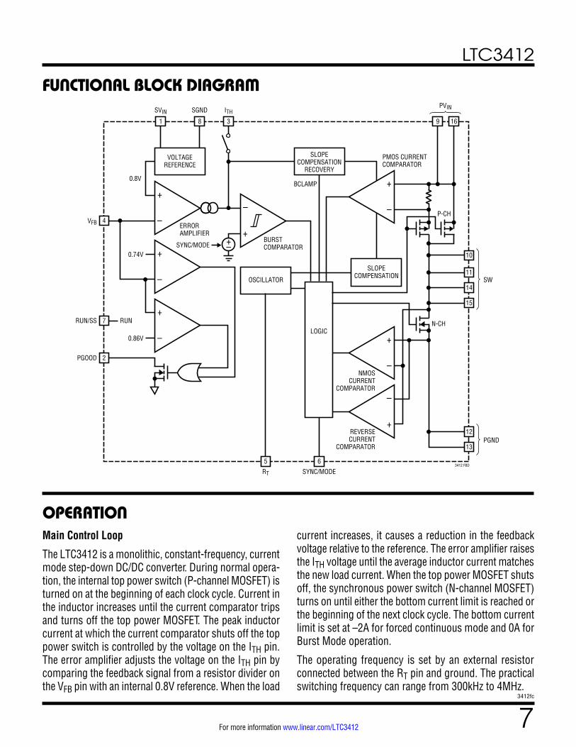
FUNCTIONAL BLOCK DIAGRAM
–
+
2
7
4 –
+
+
–
–
+
0.74V
ERRORAMPLIFIER
SYNC/MODEBURSTCOMPARATOR
BCLAMP
NMOSCURRENT
COMPARATOR
PMOS CURRENTCOMPARATOR
REVERSECURRENT
COMPARATOR
0.86V
RUNRUN/SS
15
13
12
14
11SW
P-CH
N-CH
10
PGOOD
3
ITH
VFB
0.8V
5
RT
6
SYNC/MODE3412 FBD
16
PVIN
98
SGND
1
SVIN
SLOPECOMPENSATION
VOLTAGEREFERENCE
OSCILLATOR
LOGIC
SLOPECOMPENSATION
RECOVERY
–
+
–
+
+
–
PGND
+–
OPERATIONMain Control Loop
The LTC3412 is a monolithic, constant-frequency, current mode step-down DC/DC converter. During normal opera-tion, the internal top power switch (P-channel MOSFET) is turned on at the beginning of each clock cycle. Current in the inductor increases until the current comparator trips and turns off the top power MOSFET. The peak inductor current at which the current comparator shuts off the top power switch is controlled by the voltage on the ITH pin. The error amplifier adjusts the voltage on the ITH pin by comparing the feedback signal from a resistor divider on the VFB pin with an internal 0.8V reference. When the load
current increases, it causes a reduction in the feedback voltage relative to the reference. The error amplifier raises the ITH voltage until the average inductor current matches the new load current. When the top power MOSFET shuts off, the synchronous power switch (N-channel MOSFET) turns on until either the bottom current limit is reached or the beginning of the next clock cycle. The bottom current limit is set at –2A for forced continuous mode and 0A for Burst Mode operation.
The operating frequency is set by an external resistor connected between the RT pin and ground. The practical switching frequency can range from 300kHz to 4MHz.
LTC3412
83412fc
For more information www.linear.com/LTC3412
OPERATIONOvervoltage and undervoltage comparators will pull the PGOOD output low if the output voltage comes out of regulation by ±7.5%. In an overvoltage condition, the top power MOSFET is turned off and the bottom power MOSFET is switched on until either the overvoltage con-dition clears or the bottom MOSFET’s current limit is reached.
Forced Continuous Mode
Connecting the SYNC/MODE pin to SVIN will disable Burst Mode operation and force continuous current operation. At light loads, forced continuous mode operation is less efficient than Burst Mode operation but may be desirable in some applications where it is necessary to keep switch-ing harmonics out of a signal band. The output voltage ripple is minimized in this mode.
Burst Mode Operation
Connecting the SYNC/MODE pin to a voltage between 0V to 1V enables Burst Mode operation. In Burst Mode operation, the internal power MOSFETs operate intermit-tently at light loads. This increases efficiency by minimiz-ing switching losses. During Burst Mode operation, the minimum peak inductor current is externally set by the voltage on the SYNC/MODE pin and the voltage on the ITH pin is monitored by the burst comparator to deter-mine when sleep mode is enabled and disabled. When the average inductor current is greater than the load current, the voltage on the ITH pin drops. As the ITH voltage falls below 150mV, the burst comparator trips and enables sleep mode. During sleep mode, the top MOSFET is held off and the ITH pin is disconnected from the output of the error amplifier. The majority of the internal circuitry is also turned off to reduce the quiescent current to 62µA while the load current is solely supplied by the output capacitor. When the output voltage drops, the ITH pin is reconnected to the output of the error amplifier and the top power MOSFET along with all the internal circuitry is switched back on. This process repeats at a rate that is dependent on the load demand.
Pulse skipping operation can be implemented by connect-ing the SYNC/MODE pin to ground. This forces the burst clamp level to be at 0V. As the load current decreases, the
peak inductor current will be determined by the voltage on the ITH pin until the ITH voltage drops below 200mV. At this point, the peak inductor current is determined by the minimum on-time of the current comparator. If the load demand is less than the average of the minimum on-time inductor current, switching cycles will be skipped to keep the output voltage in regulation.
Frequency Synchronization
The internal oscillator of the LTC3412 can be synchro-nized to an external clock connected to the SYNC/MODE pin. The frequency of the external clock can be in the range of 300kHz to 4MHz. For this application, the oscil-lator timing resistor should be chosen to correspond to a frequency that is 25% lower than the synchronization frequency. During synchronization, the burst clamp is set to 0V and each switching cycle begins at the falling edge of the external clock signal.
Dropout Operation
When the input supply voltage decreases toward the out-put voltage, the duty cycle increases toward the maximum on-time. Further reduction of the supply voltage forces the main switch to remain on for more than one cycle eventually reaching 100% duty cycle. The output voltage will then be determined by the input voltage minus the voltage drop across the internal P-channel MOSFET and the inductor.
Low Supply Operation
The LTC3412 is designed to operate down to an input sup-ply voltage of 2.625V. One important consideration at low input supply voltages is that the RDS(ON) of the P-channel and N-channel power switches increases. The user should calculate the power dissipation when the LTC3412 is used at 100% duty cycle with low input voltages to ensure that thermal limits are not exceeded.
Slope Compensation and Inductor Peak Current
Slope compensation provides stability in constant fre-quency architectures by preventing subharmonic oscilla-tions at duty cycles greater than 50%. It is accomplished internally by adding a compensating ramp to the inductor
LTC3412
93412fc
For more information www.linear.com/LTC3412
OPERATION
APPLICATIONS INFORMATION
current signal at duty cycles in excess of 40%. Normally, the maximum inductor peak current is reduced when slope compensation is added. In the LTC3412, however, slope compensation recovery is implemented to keep the maximum inductor peak current constant throughout the range of duty cycles. This keeps the maximum output cur-rent relatively constant regardless of duty cycle.
Short-Circuit Protection
When the output is shorted to ground, the inductor cur-rent decays very slowly during a single switching cycle. To prevent current runaway from occurring, a secondary current limit is imposed on the inductor current. If the inductor valley current increases larger than 4.8A, the top power MOSFET will be held off and switching cycles will be skipped until the inductor current falls to a safe level.
The basic LTC3412 application circuit is shown in Figure 1. External component selection is determined by the maximum load current and begins with the selection of the inductor value and operating frequency followed by CIN and COUT.
Operating Frequency
Selection of the operating frequency is a tradeoff between efficiency and component size. High frequency operation allows the use of smaller inductor and capacitor values. Operation at lower frequencies improves efficiency by reducing internal gate charge and switching losses but requires larger inductance values and/or capacitance to maintain low output ripple voltage.
The operating frequency of the LTC3412 is determined by an external resistor that is connected between the RT pin and ground. The value of the resistor sets the ramp current that is used to charge and discharge an internal timing capacitor within the oscillator and can be calcu-lated by using the following equation:
ROSC =
3.23•1011
f(Hz)(Ω)−10kΩ
Although frequencies as high as 4MHz are possible, the minimum on-time of the LTC3412 imposes a minimum limit on the operating duty cycle. The minimum on-time is typically 110ns. Therefore, the minimum duty cycle is equal to 100 • 110ns • f(Hz).
Inductor Selection
For a given input and output voltage, the inductor value and operating frequency determine the ripple current. The ripple current ∆IL increases with higher VIN and decreases with higher inductance.
ΔIL =
VOUTfL
⎡
⎣⎢⎤
⎦⎥1− VOUT
VIN
⎡
⎣⎢
⎤
⎦⎥
Having a lower ripple current reduces the ESR losses in the output capacitors and the output voltage ripple. Highest efficiency operation is achieved at low frequency with small ripple current. This, however, requires a large inductor.
A reasonable starting point for selecting the ripple current is ∆IL = 0.4(IMAX). The largest ripple current occurs at the highest VIN. To guarantee that the ripple current stays below a specified maximum, the inductor value should be chosen according to the following equation:
L= VOUT
fΔIL(MAX)
⎛
⎝⎜⎜
⎞
⎠⎟⎟ 1−
VOUTVIN(MAX)
⎛
⎝⎜⎜
⎞
⎠⎟⎟
The inductor value will also have an effect on Burst Mode operation. The transition from low current operation begins when the peak inductor current falls below a level set by the burst clamp. Lower inductor values result in higher ripple current which causes this to occur at lower load currents. This causes a dip in efficiency in the upper range of low current operation. In Burst Mode operation, lower induc-tance values will cause the burst frequency to increase.
LTC3412
103412fc
For more information www.linear.com/LTC3412
APPLICATIONS INFORMATIONInductor Core Selection
Once the value for L is known, the type of inductor must be selected. High efficiency converters generally cannot afford the core loss found in low cost powdered iron cores, forcing the use of more expensive ferrite, mol-lypermalloy, or Kool Mµ® cores. Actual core loss is inde-pendent of core size for a fixed inductor value but it is very dependent on the inductance selected. As the inductance increases, core losses decrease. Unfortunately, increased inductance requires more turns of wire and therefore cop-per losses will increase.
Ferrite designs have very low core losses and are pre-ferred at high switching frequencies, so design goals can concentrate on copper loss and preventing saturation. Ferrite core material saturates “hard,” which means that inductance collapses abruptly when the peak design cur-rent is exceeded. This results in an abrupt increase in inductor ripple current and consequent output voltage ripple. Do not allow the core to saturate!
Different core materials and shapes will change the size/current and price/current relationship of an induc-tor. Toroid or shielded pot cores in ferrite or permalloy materials are small and don’t radiate energy but generally cost more than powdered iron core inductors with similar characteristics. The choice of which style inductor to use mainly depends on the price vs size requirements and any radiated field/EMI requirements. New designs for surface mount inductors are available from Coiltronics, Coilcraft, Toko and Sumida.
CIN and COUT Selection
The input capacitance, CIN, is needed to filter the trapezoi-dal current at the source of the top MOSFET. To prevent large ripple voltage, a low ESR input capacitor sized for the maximum RMS current should be used. RMS current is given by:
IRMS =IOUT(MAX)
VOUTVIN
VINVOUT
−1
This formula has a maximum at VIN = 2VOUT, where IRMS = IOUT/2. This simple worst-case condition is commonly used for design because even significant deviations do
not offer much relief. Note that ripple current ratings from capacitor manufacturers are often based on only 2000 hours of life which makes it advisable to further derate the capacitor, or choose a capacitor rated at a higher tempera-ture than required. Several capacitors may also be paral-leled to meet size or height requirements in the design.
The selection of COUT is determined by the effective series resistance (ESR) that is required to minimize voltage rip-ple and load step transients, as well as the amount of bulk capacitance that is necessary to ensure that the control loop is stable. Loop stability can be checked by viewing the load transient response as described in a later section. The output ripple, ∆VOUT, is determined by:
ΔVOUT ≤ΔIL ESR+ 1
8fCOUT
⎛
⎝⎜
⎞
⎠⎟
The output ripple is highest at maximum input voltage since ∆IL increases with input voltage. Multiple capacitors placed in parallel may be needed to meet the ESR and RMS current handling requirements. Dry tantalum, spe-cial polymer, aluminum electrolytic and ceramic capaci-tors are all available in surface mount packages. Special polymer capacitors offer very low ESR but have lower capacitance density than other types. Tantalum capacitors have the highest capacitance density but it is important to only use types that have been surge tested for use in switching power supplies. Aluminum electrolytic capaci-tors have significantly higher ESR but can be used in cost-sensitive applications provided that consideration is given to ripple current ratings and long term reliability. Ceramic capacitors have excellent low ESR characteristics but can have a high voltage coefficient and audible piezoelectric effects. The high Q of ceramic capacitors with trace induc-tance can also lead to significant ringing.
Using Ceramic Input and Output Capacitors
Higher values, lower cost ceramic capacitors are now becoming available in smaller case sizes. Their high ripple current, high voltage rating and low ESR make them ideal for switching regulator applications. However, care must be taken when these capacitors are used at the input and output. When a ceramic capacitor is used at the input and
LTC3412
113412fc
For more information www.linear.com/LTC3412
APPLICATIONS INFORMATIONthe power is supplied by a wall adapter through long wires, a load step at the output can induce ringing at the input, VIN. At best, this ringing can couple to the output and be mistaken as loop instability. At worst, a sudden inrush of current through the long wires can potentially cause a voltage spike at VIN large enough to damage the part.
Output Voltage Programming
The output voltage is set by an external resistive divider according to the following equation:
VOUT =0.8V 1+R2
R1⎛
⎝⎜
⎞
⎠⎟
The resistive divider allows the VFB pin to sense a fraction of the output voltage as shown in Figure 2.
LTC3412
VFB
VOUT
SGND
3412 F02
R2
R1
Figure 2. Setting the Output Voltage
Burst Clamp Programming
If the voltage on the SYNC/MODE pin is less than VIN by 1V, Burst Mode operation is enabled. During Burst Mode operation, the voltage on the SYNC/MODE pin determines the burst clamp level which sets the minimum peak induc-tor current, IBURST, for each switching cycle according to the following equation:
IBURST = VBURST −0.2V( ) 3.75A
0.8V⎛
⎝⎜
⎞
⎠⎟
VBURST is the voltage on the SYNC/MODE pin. IBURST can be programmed in the range of 0A to 3.75A. For values of VBURST greater than 1V, IBURST is set at 3.75A. For values of VBURST less than 0.2V, IBURST is set at 0A. As the output load current drops, the peak inductor current decreases to keep the output voltage in regulation. When the output load current demands a peak inductor current that is less than IBURST, the burst clamp will force the peak
inductor current to remain equal to IBURST regardless of further reductions in the load current. Since the average inductor current is greater than the output load current, the voltage on the ITH pin will decrease. When the ITH voltage drops to 150mV, sleep mode is enabled in which both power MOSFETs are shut off along with most of the circuitry to minimize power consumption. All circuitry is turned back on and the power MOSFETs begin switching again when the output voltage drops out of regulation. The value for IBURST is determined by the desired amount of output voltage ripple. As the value of IBURST increases, the sleep period between pulses and the output voltage ripple increase. The burst clamp voltage, VBURST, can be set by a resistor divider from the VFB pin to the SGND pin as shown in Figure 1.
Pulse skipping, which is a compromise between low output voltage ripple and efficiency, can be implemented by connecting the SYNC/MODE pin to ground. This sets IBURST to 0A. In this condition, the peak inductor current is limited by the minimum on-time of the current comparator, and the lowest output voltage ripple is achieved while still operating discontinuously. During very light output loads, pulse skipping allows only a few switching cycles to be skipped while maintaining the output voltage in regulation.
Frequency Synchronization
The LTC3412’s internal oscillator can be synchronized to an external clock signal. During synchronization, the top MOSFET turn-on is locked to the falling edge of the external frequency source. The synchronization frequency range is 300kHz to 4MHz. Synchronization only occurs if the external frequency is greater than the frequency set by the external resistor. Because slope compensation is generated by the oscillator’s RC circuit, the external frequency should be set 25% higher than the frequency set by the external resistor to ensure that adequate slope compensation is present.
Soft-Start
The RUN/SS pin provides a means to shut down the LTC3412 as well as a timer for soft-start. Pulling the RUN/SS pin below 0.5V places the LTC3412 in a low quiescent current shutdown state (IQ < 1µA).
LTC3412
123412fc
For more information www.linear.com/LTC3412
APPLICATIONS INFORMATIONThe LTC3412 contains an internal soft-start clamp that gradually raises the clamp on ITH after the RUN/SS pin is pulled above 2V. The full current range becomes available on ITH after 1024 switching cycles. If a longer soft-start period is desired, the clamp on ITH can be set externally with a resistor and capacitor on the RUN/SS pin as shown in Figure 1. The soft-start duration can be calculated by using the following formula:
tSS =RSSCSS ln VIN
VIN−1.8V
⎛
⎝⎜
⎞
⎠⎟ Seconds( )
Efficiency Considerations
The efficiency of a switching regulator is equal to the out-put power divided by the input power times 100%. It is often useful to analyze individual losses to determine what is limiting the efficiency and which change would produce the most improvement. Efficiency can be expressed as:
Efficiency = 100% – (L1 + L2 + L3 + ...)
where L1, L2, etc. are the individual losses as a percent-age of input power.
Although all dissipative elements in the circuit produce losses, two main sources usually account for most of the losses: VIN quiescent current and I2R losses.
The VIN quiescent current loss dominates the efficiency loss at very low load currents whereas the I2R loss domi-nates the efficiency loss at medium to high load currents. In a typical efficiency plot, the efficiency curve at very low load currents can be misleading since the actual power lost is of no consequence.
1. The VIN quiescent current is due to two components: the DC bias current as given in the electrical characteris-tics and the internal main switch and synchronous switch gate charge currents. The gate charge current results from switching the gate capacitance of the internal power MOSFET switches. Each time the gate is switched from high to low to high again, a packet of charge dQ moves from VIN to ground. The resulting dQ/dt is the current out of VIN that is typically larger than the DC bias current. In continuous mode, IGATECHG=f(QT + QB) where QT and
QB are the gate charges of the internal top and bottom switches. Both the DC bias and gate charge losses are proportional to VIN and thus their effects will be more pronounced at higher supply voltages.
2. I2R losses are calculated from the resistances of the internal switches, RSW and external inductor RL. In con-tinuous mode the average output current flowing through inductor L is “chopped” between the main switch and the synchronous switch. Thus, the series resistance looking into the SW pin is a function of both top and bottom MOSFET RDS(ON) and the duty cycle (DC) as follows:
RSW = (RDS(ON)TOP)(DC) + (RDS(ON)BOT)(1 – DC)
The RDS(ON) for both the top and bottom MOSFETs can be obtained from the Typical Performance Characteristics curves. Thus, to obtain I2R losses, simply add RSW to RL and multiply the result by the square of the average output current.
Other losses including CIN and COUT ESR dissipative losses and inductor core losses generally account for less than 2% of the total loss.
Thermal Considerations
In most applications, the LTC3412 does not dissipate much heat due to its high efficiency. But, in applications where the LTC3412 is running at high ambient tempera-ture with low supply voltage and high duty cycles, such as in dropout, the heat dissipated may exceed the maxi-mum junction temperature of the part. If the junction temperature reaches approximately 150°C, both power switches will be turned off and the SW node will become high impedance.
To avoid the LTC3412 from exceeding the maximum junc-tion temperature, the user will need to do some thermal analysis. The goal of the thermal analysis is to determine whether the power dissipated exceeds the maximum junc-tion temperature of the part. The temperature rise is given by:
TR = (PD)(θJA)
where PD is the power dissipated by the regulator and θJA is the thermal resistance from the junction of the die to the ambient temperature.
LTC3412
133412fc
For more information www.linear.com/LTC3412
APPLICATIONS INFORMATIONThe junction temperature, TJ, is given by:
TJ = TA + TR
where TA is the ambient temperature.
As an example, consider the LTC3412 in dropout at an input voltage of 3.3V, a load current of 2.5A and an ambi-ent temperature of 70°C. From the typical performance graph of switch resistance, the RDS(ON) of the P-channel switch at 70°C is approximately 97mΩ. Therefore, power dissipated by the part is:
PD = (ILOAD2)(RDS(ON)) = (2.5A)2(97mΩ) = 0.61W
For the TSSOP package, the θJA is 37.6°C/W. Thus the junction temperature of the regulator is:
TJ = 70°C + (0.61W)(37.6°C/W) = 93°C
which is below the maximum junction temperature of 125°C.
Note that at higher supply voltages, the junction tempera-ture is lower due to reduced switch resistance (RDS(ON)).
Checking Transient Response
The regulator loop response can be checked by look-ing at the load transient response. Switching regulators take several cycles to respond to a step in load current. When a load step occurs, VOUT immediately shifts by an amount equal to ∆ILOAD(ESR), where ESR is the effective series resistance of COUT. ∆ILOAD also begins to charge or discharge COUT generating a feedback error signal used by the regulator to return VOUT to its steady-state value. During this recovery time, VOUT can be monitored for overshoot or ringing that would indicate a stability prob-lem. The ITH pin external components and output capaci-tor shown in Figure 1 will provide adequate compensation for most applications.
Design Example
As a design example, consider using the LTC3412 in an application with the following specifications: VIN = 2.7V to 4.2V, VOUT = 2.5V, IOUT(MAX) = 2.5A, IOUT(MIN) = 10mA, f = 1MHz. Because efficiency is important at both high and low load current, Burst Mode operation will be utilized.
First, calculate the timing resistor:
ROSC =
3.23•1011
1•106 −10k=313k
Use a standard value of 309k. Next, calculate the inductor value for about 40% ripple current at maximum VIN:
L= 2.5V
(1MHz)(1A)
⎛
⎝⎜
⎞
⎠⎟ 1− 2.5V
4.2V⎛
⎝⎜
⎞
⎠⎟=1.01µH
Using a 1µH inductor, results in a maximum ripple cur-rent of:
ΔIL =
2.5V(1MHz)(1µH)
⎛
⎝⎜
⎞
⎠⎟ 1− 2.5V
4.2V⎛
⎝⎜
⎞
⎠⎟=1.01A
COUT will be selected based on the ESR that is required to satisfy the output voltage ripple requirement and the bulk capacitance needed for loop stability. In this application, two tantalum capacitors will be used to provide the bulk capacitance and a ceramic capacitor in parallel to lower the total effective ESR. For this design, two 100µF tanta-lum capacitors in parallel with a 10µF ceramic capacitor will be used. CIN should be sized for a maximum current rating of:
IRMS= 2.5A( ) 2.5V
4.2V⎛
⎝⎜
⎞
⎠⎟
4.2V2.5V
−1=1.23ARMS
Decoupling the PVIN and SVIN pins with a 22µF ceramic capacitor and a 220µF tantalum capacitor is adequate for most applications.
The burst clamp and output voltage can now be pro-grammed by choosing the values of R1, R2 and R3. The voltage on the MODE pin will be set to 0.32V by the resis-tor divider consisting of R2 and R3. A burst clamp voltage of 0.32V will set the minimum inductor current, IBURST, as follows:
IBURST= 0.32V−0.2V( ) 3.75V
0.8V⎛
⎝⎜
⎞
⎠⎟=563mA
LTC3412
143412fc
For more information www.linear.com/LTC3412
If we set the sum of R2 and R3 to 185k, then the following equations can be solved:
R2+R3=185k
1+R2R3
=0.8V0.32V
The last two equations shown result in the following val-ues for R2 and R3: R2 = 110k , R3 = 75k. The value of R1 can now be determined by solving the equation shown below:
1+ R1185k
=2.5V0.8V
R1=393k
A value of 392k will be selected for R1. Figure 4 shows the complete schematic for this design example.
PC Board Layout Checklist
When laying out the printed circuit board, the following checklist should be used to ensure proper operation of the LTC3412. Check the following in your layout.
APPLICATIONS INFORMATION1. A ground plane is recommended. If a ground plane layer is not used, the signal and power grounds should be segregated with all small-signal components returning to the SGND pin at one point which is then connected to the PGND pin close to the LTC3412. The exposed pad should be connected to SGND.
2. Connect the (+) terminal of the input capacitor(s), CIN, as close as possible to the PVIN pin. This capacitor pro-vides the AC current into the internal power MOSFETs.
3. Keep the switching node, SW, away from all sensitive small-signal nodes.
4. Flood all unused areas on all layers with copper. Flooding with copper will reduce the temperature rise of power components. You can connect the copper areas to any DC net (PVIN, SVIN, VOUT, PGND, SGND, or any other DC rail in your system).
5. Connect the VFB pin directly to the feedback resistors. The resistor divider must be connected between VOUT and SGND.
Figure 3. LTC3412 Layout Diagram
Top Side Bottom Side
LTC3412
153412fc
For more information www.linear.com/LTC3412
APPLICATIONS INFORMATION
8SGND
CSS470pF X7R
CC100pF
***
†††
TOKO D62CB A920CY-1ROMSANYO POSCAP 4TPB100MTAIYO YUDEN LMK325BJ106MNSANYO POSCAP 2R5TPC220M
7RSS4.7M
RUN
6 SYNC/MODEROSC 309k
5RT
R2110k
4
R375k
VFB
RITH7.15k 3
CITH 680pF X7R
ITH
2PGOODPGOOD
1SVIN
9PVIN
10SW
11SW
12PGND
LTC341213 L1*
1µHPGND
14SW
15SW
16PVIN
CIN222µF
X5R 6.3V
CIN1††
220µF
COUT2†
10µF
COUT1**100µF×2
VOUT2.5V2.5A
VIN2.7V TO 4.2V
GND
3412 F04
R1 392k
+
RPG100k
CFB 22pF X5R
Figure 4. Single Lithium-Ion to 2.5V, 2.5A Regulator at 1MHz, Burst Mode Operation Using POSCAPs
LTC3412
163412fc
For more information www.linear.com/LTC3412
TYPICAL APPLICATIONS2.5V, 2.5A Regulator Using All Ceramic Capacitors
1.8V, 2.5A Step-Down Regulator at 1MHz, Burst Mode Operation
8SGND
CSS470pF X7R
7RSS4.7M
RUN
6SYNC/MODE
ROSC309k
5RT
R2110k
4
R375k
VFB
RITH15k 3
CITH 1000pF X7R
ITH
2PGOODPGOOD
1SVIN
9PVIN
10SW
11SW
12PGND
LTC341213 L1*
1µHPGND
14SW
15SW
16PVIN
C1 22pF X5R
CIN222µF
X5R 6.3V
CIN122µFX5R 6.3V
COUT**100µF
VOUT2.5V2.5A
VIN2.7V TO 5.5V
GND
3412 F05
CIN3**100µF
R1 392k
***
TOKO D62CB A920CY-1ROMTDK C4532X5R0J107M
CC100pF
RPG100k
8SGND
CSS470pF X7R
7RSS4.7M
RUN
6SYNC/MODE
ROSC309k
5RT
R2110k
R375k
4VFB
RITH10k 3
CITH 560pF X7R
ITH
2PGOODPGOOD
1SVIN
9PVIN
10SW
11SW
12PGND
LTC341213
PGND
14SW
15SW
16PVIN
CIN2 22µF**
CIN1**22µF
COUT**22µFx2
VOUT1.8V2A
VIN3.3V
GND
R1 232k
3412 TA05
L11µH*
***
SUMIDA CR431R0AVX 12066D226MAT
C247pF
C1 22pF X5R
RPG100k
LTC3412
173412fc
For more information www.linear.com/LTC3412
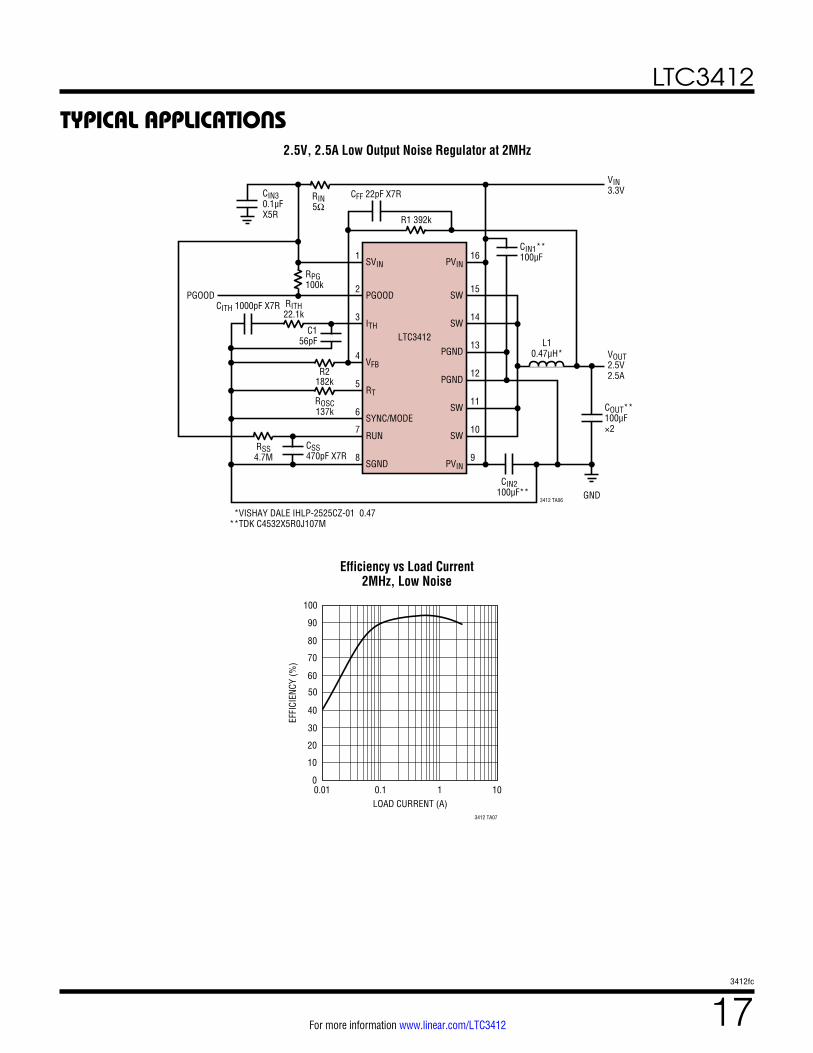
TYPICAL APPLICATIONS2.5V, 2.5A Low Output Noise Regulator at 2MHz
Efficiency vs Load Current2MHz, Low Noise
8SGND
CSS470pF X7R
7
RSS4.7M
RUN
6SYNC/MODE
ROSC137k
5RT
R2182k
4VFB
RITH22.1k 3
CITH 1000pF X7R
ITH
2PGOODPGOOD
1SVIN
9PVIN
10SW
11SW
12PGND
LTC341213
PGND
14SW
15SW
16PVIN
CIN2 100µF**
CIN1**100µF
COUT**100µF×2
VOUT2.5V2.5A
VIN3.3V
GND
R1 392k
RIN5Ω
3412 TA06
L10.47µH*
***
VISHAY DALE IHLP-2525CZ-01 0.47TDK C4532X5R0J107M
C156pF
CFF 22pF X7R
RPG100k
CIN30.1µFX5R
LOAD CURRENT (A)0.01
40
EFFI
CIEN
CY (%
)
50
60
70
80
0.1 1 10
3412 TA07
30
20
10
0
90
100
LTC3412
183412fc
For more information www.linear.com/LTC3412
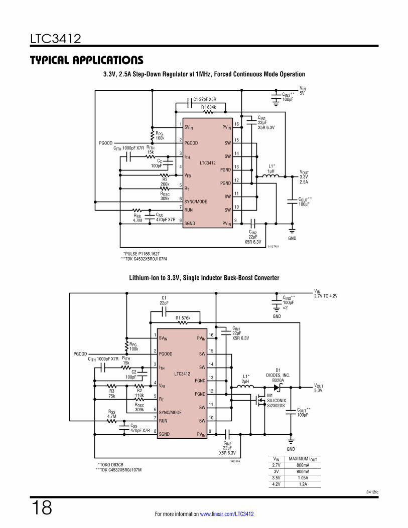
TYPICAL APPLICATIONS
8SGND
CSS470pF X7R
7
RSS4.7M
RUN
6SYNC/MODE
ROSC309k
5RT
R2200k
4
VFB
RITH15k 3
CITH 1000pF X7R
ITH
2PGOODPGOOD
1SVIN
9PVIN
10SW
11SW
12PGND
LTC341213
PGND
14SW
15SW
16PVIN
CIN222µF
X5R 6.3V
CIN122µFX5R 6.3V
COUT**100µF
VOUT3.3V2.5A
VIN5V
GND
R1 634k
3412 TA01
L1*1µH
***
PULSE P1166.162TTDK C4532X5R0J107M
CC100pF
C1 22pF X5RCIN3**100µF
RPG100k
8SGND
CSS470pF X7R
7RSS4.7M
RUN
6SYNC/MODE
ROSC309k
5RT
R2110k
4
R375k
VFB
RITH15k 3
CITH 1000pF X7R
ITH
2PGOODPGOOD
1SVIN
9PVIN
10SW
11SW
12PGND
LTC341213 L1*
2µH
M1SILICONIXSi2302DS
D1DIODES, INC.
B320APGND
14SW
15SW
16PVIN
C122pF
CIN222µF
X5R 6.3V
CIN122µFX5R 6.3V
COUT**100µF
VOUT3.3V
VIN2.7V TO 4.2V
GND
GND
3412 F04
CIN3**100µF×2
R1 576k
***
TOKO D63CBTDK C4532X5R0J107M
C2100pF
RPG100k
VIN MAXIMUM IOUT 2.7V 800mA 3V 900mA 3.5V 1.05A 4.2V 1.2A
3.3V, 2.5A Step-Down Regulator at 1MHz, Forced Continuous Mode Operation
Lithium-Ion to 3.3V, Single Inductor Buck-Boost Converter
LTC3412
193412fc
For more information www.linear.com/LTC3412
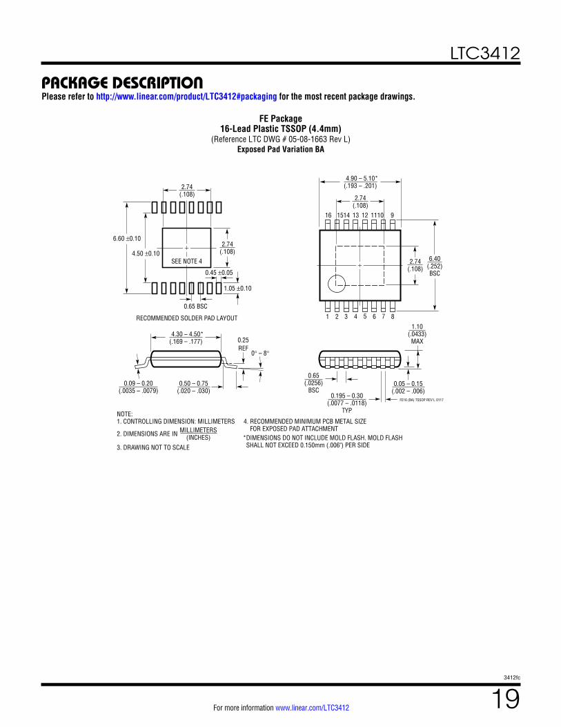
PACKAGE DESCRIPTIONPlease refer to http://www.linear.com/product/LTC3412#packaging for the most recent package drawings.
FE16 (BA) TSSOP REV L 0117
0.09 – 0.20(.0035 – .0079)
0° – 8°
0.25REF
0.50 – 0.75(.020 – .030)
4.30 – 4.50*(.169 – .177)
1 3 4 5 6 7 8
10 9
4.90 – 5.10*(.193 – .201)
16 1514 13 12 11
1.10(.0433)
MAX
0.05 – 0.15(.002 – .006)
0.65(.0256)
BSC
2.74(.108)
2.74(.108)
0.195 – 0.30(.0077 – .0118)
TYP
2
MILLIMETERS(INCHES) *DIMENSIONS DO NOT INCLUDE MOLD FLASH. MOLD FLASH
SHALL NOT EXCEED 0.150mm (.006") PER SIDE
NOTE:1. CONTROLLING DIMENSION: MILLIMETERS
2. DIMENSIONS ARE IN
RECOMMENDED SOLDER PAD LAYOUT
3. DRAWING NOT TO SCALE
0.45 ±0.05
0.65 BSC
4.50 ±0.10
6.60 ±0.10
1.05 ±0.10
2.74(.108)
2.74(.108)
SEE NOTE 4
4. RECOMMENDED MINIMUM PCB METAL SIZE FOR EXPOSED PAD ATTACHMENT
6.40(.252)BSC
FE Package16-Lead Plastic TSSOP (4.4mm)
(Reference LTC DWG # 05-08-1663 Rev L)Exposed Pad Variation BA
LTC3412
203412fc
For more information www.linear.com/LTC3412
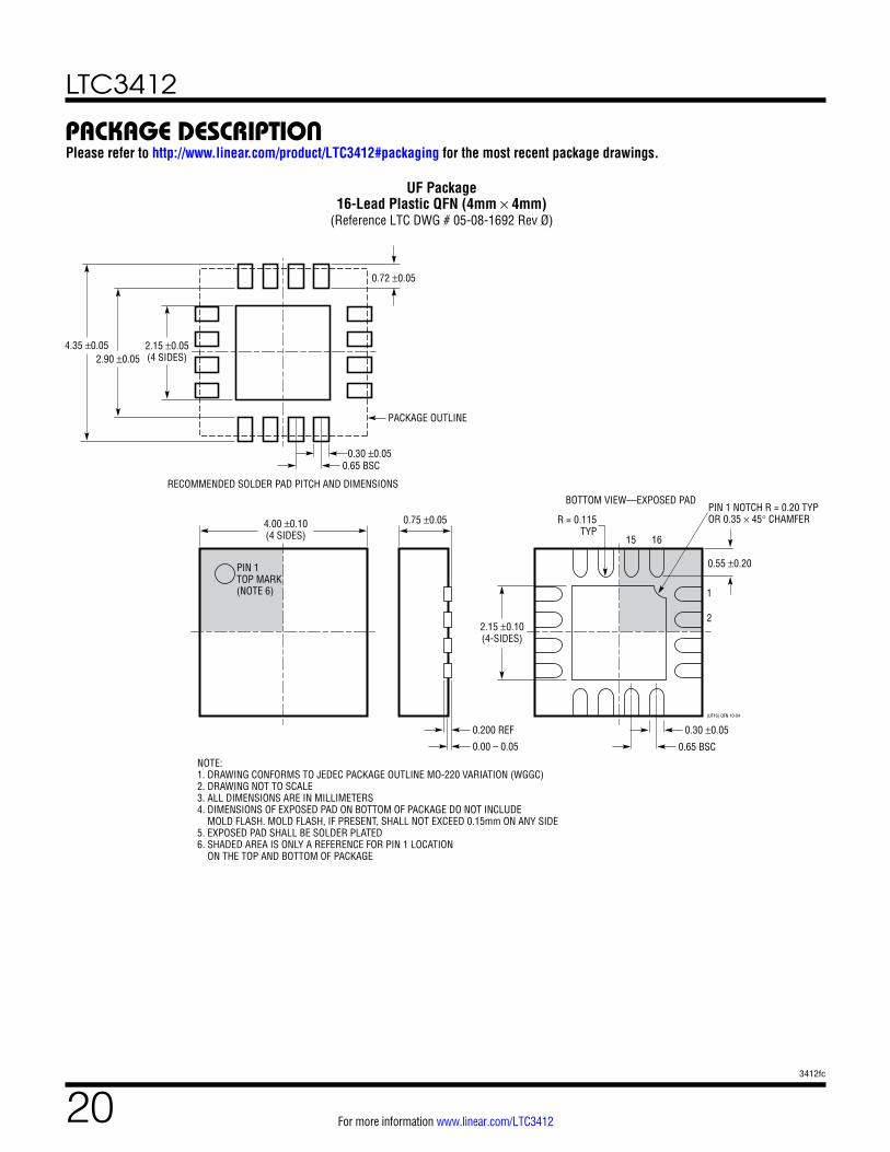
PACKAGE DESCRIPTIONPlease refer to http://www.linear.com/product/LTC3412#packaging for the most recent package drawings.
4.00 ±0.10(4 SIDES)
NOTE:1. DRAWING CONFORMS TO JEDEC PACKAGE OUTLINE MO-220 VARIATION (WGGC)2. DRAWING NOT TO SCALE3. ALL DIMENSIONS ARE IN MILLIMETERS4. DIMENSIONS OF EXPOSED PAD ON BOTTOM OF PACKAGE DO NOT INCLUDE MOLD FLASH. MOLD FLASH, IF PRESENT, SHALL NOT EXCEED 0.15mm ON ANY SIDE5. EXPOSED PAD SHALL BE SOLDER PLATED6. SHADED AREA IS ONLY A REFERENCE FOR PIN 1 LOCATION ON THE TOP AND BOTTOM OF PACKAGE
PIN 1TOP MARK(NOTE 6)
0.55 ±0.20
1615
1
2
BOTTOM VIEW—EXPOSED PAD
2.15 ±0.10(4-SIDES)
0.75 ±0.05 R = 0.115TYP
0.30 ±0.05
0.65 BSC
0.200 REF
0.00 – 0.05
(UF16) QFN 10-04
RECOMMENDED SOLDER PAD PITCH AND DIMENSIONS
0.72 ±0.05
0.30 ±0.050.65 BSC
2.15 ±0.05(4 SIDES)2.90 ±0.05
4.35 ±0.05
PACKAGE OUTLINE
PIN 1 NOTCH R = 0.20 TYPOR 0.35 × 45° CHAMFER
UF Package16-Lead Plastic QFN (4mm × 4mm)
(Reference LTC DWG # 05-08-1692 Rev Ø)
LTC3412
213412fc
For more information www.linear.com/LTC3412
Information furnished by Linear Technology Corporation is believed to be accurate and reliable. However, no responsibility is assumed for its use. Linear Technology Corporation makes no representa-tion that the interconnection of its circuits as described herein will not infringe on existing patent rights.
REVISION HISTORYREV DATE DESCRIPTION PAGE NUMBER
C 05/17 Add Storage Temperature to Absolute Maximum Ratings 2
(Revision history begins at Rev C)
LTC3412
223412fc
LINEAR TECHNOLOGY CORPORATION 2002
LT 0517 REV C • PRINTED IN USAwww.linear.com/LTC3412
RELATED PARTS
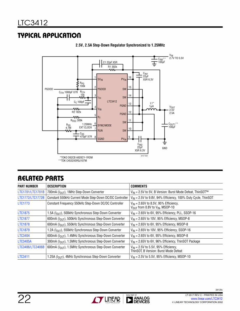
TYPICAL APPLICATION
PART NUMBER DESCRIPTION COMMENTS
LTC1701/LTC1701B 700mA (IOUT), 1MHz Step-Down Converter VIN = 2.5V to 5V, B Version: Burst Mode Defeat, ThinSOT™
LTC1772/LTC1772B Constant 550kHz Current Mode Step-Down DC/DC Controller VIN = 2.5V to 9.8V, 94% Efficiency, 100% Duty Cycle, ThinSOT
LTC1773 Constant Frequency 550kHz Step-Down DC/DC Controller VIN = 2.65V to 8.5V, 95% Efficiency, VOUT from 0.8V to VIN, MSOP-10
LTC1875 1.5A (IOUT), 500kHz Synchronous Step-Down Converter VIN = 2.65V to 6V, 95% Efficiency, PLL, SSOP-16
LTC1877 600mA (IOUT), 500kHz Synchronous Step-Down Converter VIN = 2.65V to 10V, 95% Efficiency, MSOP-8
LTC1878 600mA (IOUT), 550kHz Synchronous Step-Down Converter VIN = 2.65V to 6V, 95% Efficiency, MSOP-8
LTC1879 1.2A (IOUT), 550kHz Synchronous Step-Down Converter VIN = 2.65V to 10V, 95% Efficiency, SSOP-16
LTC3404 600mA (IOUT), 1.4MHz Synchronous Step-Down Converter VIN = 2.65V to 6V, 95% Efficiency, MSOP-8
LTC3405A 300mA (IOUT), 1.5MHz Synchronous Step-Down Converter VIN = 2.65V to 6V, 96% Efficiency, ThinSOT Package
LTC3406/LTC3406B 600mA (IOUT), 1.5MHz Synchronous Step-Down Converter VIN = 2.5V to 5.5V, 95% Efficiency, ThinSOT, B Version: Burst Mode Defeat
LTC3411 1.25A (IOUT), 4MHz Synchronous Step-Down Converter VIN = 2.5V to 5.5V, 95% Efficiency, MSOP-10
8SGND
CSS470pF X7R
7RSS4.7M
RUN
6SYNC/MODE1.25MHz
EXT CLOCK
ROSC 309k
5RT
R2 182k
4VFB
RITH15k
RPG100k
3CITH 1000pF X7R
ITH
2PGOODPGOOD
1SVIN
9PVIN
10SW
11SW
12PGND
LTC341213 L1*
1µHPGND
14SW
15SW
16PVIN
CIN222µF
X5R 6.3V
CIN122µFX5R 6.3V
COUT1**100µF
VOUT2.5V2.5A
VIN2.7V TO 5.5V
GND
R1 392k
3412 TA02*
**TOKO D62CB A920CY-1ROMTDK C4532X5R0J107M
CC 100pF
C1 22pF X5RCIN3**100µF
2.5V, 2.5A Step-Down Regulator Synchronized to 1.25MHz