lt1999-10/ll lt1999-50 high voltage, bidirectional current
TRANSCRIPT

LT1999-10/LT1999-20/LT1999-50
11999f
TYPICAL APPLICATION
FEATURES DESCRIPTION
High Voltage, Bidirectional Current Sense Amplifier
The LT®1999 is a high speed precision current sense amplifi er, designed to monitor bidirectional currents over a wide common mode range. The LT1999 is offered in three gain options: 10V/V, 20V/V, and 50V/V.
The LT1999 senses current via an external resistive shunt and generates an output voltage, indicating both magnitude and direction of the sensed current. The output voltage is referenced halfway between the supply voltage and ground, or an external voltage can be used to set the reference level. With a 2MHz bandwidth and a common mode input range of –5V to 80V, the LT1999 is suitable for monitoring currents in H-Bridge motor controls, switching power supplies, solenoid currents, and battery charge currents from full charge to depletion.
The LT1999 operates from an independent 5V supply and draws 1.55mA. A shutdown mode is provided for minimiz-ing power consumption.
The LT1999 is available in an 8-lead MSOP or SOP package.L, LT, LTC, LTM, Linear Technology and the Linear logo are registered trademarks of Linear Technology Corporation. All other trademarks are the property of their respective owners.
APPLICATIONS
n Buffered Output with 3 Gain Options: 10V/V, 20V/V, 50V/V
n Gain Accuracy: 0.5% Maxn Input Common Mode Voltage Range: –5V to 80Vn AC CMRR > 80dB at 100kHz n Input Offset Voltage: 1.5mV Maxn –3dB Bandwidth: 2MHzn Smooth, Continuous Operation Over Entire Common
Mode Rangen 4kV HBM Tolerant and 1kV CDM Tolerantn Low Power Shutdown <10μAn –55°C to 150°C Operating Temperature Rangen 8-Lead MSOP and 8-Lead SO (Narrow) Packages
n High Side or Low Side Current Sensingn H-Bridge Motor Controln Solenoid Current Sensen High Voltage Data Acquisitionn PWM Control Loopsn Fuse/MOSFET Monitoring
Full Bridge Armature Current Monitor
TIME (10μs/DIV)
2.5V
VO
UT (
2V
/DIV
) V+
IN (2
0V
/DIV
)
1999 TA01b
VOUTVOUT
V+IN
LT1999
4k
0.8k
160k
160k
2μA
0.8k4k
SHDN
5V
V+
V+
V+5V
RS
1999 TA01a
+
–
+
–
VS
81
2
3
4
7
6
5
0.1μF
0.1μF
VOUT
RG
V+IN
V–IN
VREF
VSHDN
V+
V+
查询LT1999-50供应商

LT1999-10/LT1999-20/LT1999-50
21999f
ABSOLUTE MAXIMUM RATINGSDifferential Input Voltage +IN to –IN (Notes 1, 3) ................................. ±60V, 10ms+IN to GND, –IN to GND (Note 2) ............. –5.25V to 88VTotal Supply Voltage (V+ to GND) ................................6VInput Voltage Pins 6 and 8 ...................V+ + 0.3V, –0.3VOutput Short-Circuit Duration (Note 4) ............ IndefiniteOperating Ambient Temperature (Note 5)
LT1999C ..............................................–40°C to 85°CLT1999I ................................................–40°C to 85°CLT1999H ............................................ –40°C to 125°CLT1999MP ......................................... –55°C to 150°C
(Note 1)
1
2
3
4
V+
+IN
–IN
V+
8
7
6
5
SHDN
OUT
REF
GND
TOP VIEW
MS8 PACKAGE8-LEAD PLASTIC MSOP
TJMAX = 150°C, ΘJA = 300°C/W
1
2
3
4
8
7
6
5
TOP VIEW
SHDN
OUT
REF
GND
V+
+IN
–IN
V+
S8 PACKAGE8-LEAD PLASTIC SO
TJMAX = 150°C, ΘJA = 190°C/W
PIN CONFIGURATION
ORDER INFORMATIONLEAD FREE FINISH TAPE AND REEL PART MARKING* PACKAGE DESCRIPTION SPECIFIED TEMPERATURE RANGE
LT1999CMS8-10#PBF LT1999CMS8-10#TRPBF LTFPB 8-Lead Plastic MSOP 0°C to 70°C
LT1999IMS8-10#PBF LT1999IMS8-10#TRPBF LTFPB 8-Lead Plastic MSOP –40°C to 85°C
LT1999HMS8-10#PBF LT1999HMS8-10#TRPBF LTFPB 8-Lead Plastic MSOP –40°C to 125°C
LT1999MPMS8-10#PBF LT1999MPMS8-10#TRPBF LTFQP 8-Lead Plastic MSOP –55°C to 150°C
LT1999CS8-10#PBF LT1999CS8-10#TRPBF 199910 8-Lead Plastic SO 0°C to 70°C
LT1999IS8-10#PBF LT1999IS8-10#TRPBF 199910 8-Lead Plastic SO –40°C to 85°C
LT1999HS8-10#PBF LT1999HS8-10#TRPBF 199910 8-Lead Plastic SO –40°C to 125°C
LT1999MPS8-10#PBF LT1999MPS8-10#TRPBF 99MP10 8-Lead Plastic SO –55°C to 150°C
LT1999CMS8-20#PBF LT1999CMS8-20#TRPBF LTFNZ 8-Lead Plastic MSOP 0°C to 70°C
LT1999IMS8-20#PBF LT1999IMS8-20#TRPBF LTFNZ 8-Lead Plastic MSOP –40°C to 85°C
LT1999HMS8-20#PBF LT1999HMS8-20#TRPBF LTFNZ 8-Lead Plastic MSOP –40°C to 125°C
LT1999MPMS8-20#PBF LT1999MPMS8-20#TRPBF LTFQQ 8-Lead Plastic MSOP –55°C to 150°C
Specified Temperature Range (Note 6)LT1999C .................................................. 0°C to 70°CLT1999I ................................................–40°C to 85°CLT1999H ............................................ –40°C to 125°CLT1999MP ......................................... –55°C to 150°C
Junction Temperature ........................................... 150°CStorage Temperature Range .................. –65°C to 150°C
查询LT1999-50供应商

LT1999-10/LT1999-20/LT1999-50
31999f
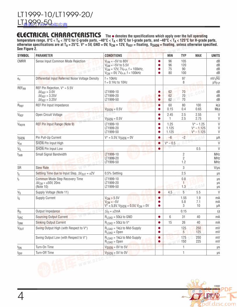
ELECTRICAL CHARACTERISTICS The l denotes the specifications which apply over the full operating temperature range, 0°C < TA < 70°C for C-grade parts, –40°C < TA < 85°C for I-grade parts, and –40°C < TA < 125°C for H-grade parts, otherwise specifications are at TA = 25°C. V+ = 5V, GND = 0V, VCM = 12V, VREF = floating, VSHDN = floating, unless otherwise specified. See Figure 2.
LEAD FREE FINISH TAPE AND REEL PART MARKING* PACKAGE DESCRIPTION SPECIFIED TEMPERATURE RANGE
LT1999CS8-20#PBF LT1999CS8-20#TRPBF 199920 8-Lead Plastic SO 0°C to 70°C
LT1999IS8-20#PBF LT1999IS8-20#TRPBF 199920 8-Lead Plastic SO –40°C to 85°C
LT1999HS8-20#PBF LT1999HS8-20#TRPBF 199920 8-Lead Plastic SO –40°C to 125°C
LT1999MPS8-20#PBF LT1999MPS8-20#TRPBF 99MP20 8-Lead Plastic SO –55°C to 150°C
LT1999CMS8-50#PBF LT1999CMS8-50#TRPBF LTFPC 8-Lead Plastic MSOP 0°C to 70°C
LT1999IMS8-50#PBF LT1999IMS8-50#TRPBF LTFPC 8-Lead Plastic MSOP –40°C to 85°C
LT1999HMS8-50#PBF LT1999HMS8-50#TRPBF LTFPC 8-Lead Plastic MSOP –40°C to 125°C
LT1999MPMS8-50#PBF LT1999MPMS8-50#TRPBF LTFQR 8-Lead Plastic MSOP –55°C to 150°C
LT1999CS8-50#PBF LT1999CS8-50#TRPBF 199950 8-Lead Plastic SO 0°C to 70°C
LT1999IS8-50#PBF LT1999IS8-50#TRPBF 199950 8-Lead Plastic SO –40°C to 85°C
LT1999HS8-50#PBF LT1999HS8-50#TRPBF 199950 8-Lead Plastic SO –40°C to 125°C
LT1999MPS8-50#PBF LT1999MPS8-50#TRPBF 99MP50 8-Lead Plastic SO –55°C to 150°C
Consult LTC Marketing for parts specified with wider operating temperature ranges. *The temperature grade is identified by a label on the shipping container.
Consult LTC Marketing for information on non-standard lead based finish parts.
For more information on lead free part marking, go to: http://www.linear.com/leadfree/ For more information on tape and reel specifications, go to: http://www.linear.com/tapeandreel/
ORDER INFORMATION
SYMBOL PARAMETER CONDITIONS MIN TYP MAX UNITS
VSENSE Full-Scale Input Sense Voltage (Note 7)VSENSE = V+IN – V–IN
LT1999-10LT1999-20LT1999-50
l
l
l
–0.35–0.2–0.08
0.350.2
0.08
VVV
VCM CM Input Voltage Range l –5 80 V
RIN(DIFF) Differential Input Impedance ΔVINDIFF = ±2V/Gain l 6.4 8 9.6 kΩ
RINCM CM Input Impedance ΔVCM = 5.5V to 80VΔVCM = –5V to 4.5V
l
l
53.6
204.8 6
MΩkΩ
VOSI Input Referred Voltage Offsetl
–750–1500
±500 7501500
μVμV
ΔVOSI /ΔT Input Referred Voltage Offset Drift 5 μV/°C
AV Gain LT1999-10LT1999-20LT1999-50
l
l
l
9.9519.9
48.75
102050
10.0520.150.25
V/VV/VV/V
AV Error Gain Error ΔVOUT = ±2V l –0.5 ±0.2 0.5 %
IB Input Bias CurrentI(+IN) = I(–IN)(Note 8)
VCM > 5.5VVCM = –5VVSHDN = 0.5V, 0V < VCM < 80V
l
l
l
100–2.35
137.5–1.950.001
175–1.52.5
μAmAμA
IOS Input Offset CurrentIOS = I(+IN) – I(–IN)(Note 8)
VCM > 5.5VVCM = –5VVSHDN = 0.5V, 0V < VCM < 80V
l
l
l
–1–10–2.5
1102.5
μAμAμA
PSRR Supply Rejection Ratio V+ = 4.5V to 5.5V l 68 77 dB
查询LT1999-50供应商
LT1999-10/LT1999-20/LT1999-50
41999f
ELECTRICAL CHARACTERISTICS The l denotes the specifications which apply over the full operating temperature range, 0°C < TA < 70°C for C-grade parts, –40°C < TA < 85°C for I-grade parts, and –40°C < TA < 125°C for H-grade parts, otherwise specifications are at TA = 25°C. V+ = 5V, GND = 0V, VCM = 12V, VREF = floating, VSHDN = floating, unless otherwise specified. See Figure 2.
SYMBOL PARAMETER CONDITIONS MIN TYP MAX UNITS
CMRR Sense Input Common Mode Rejection VCM = –5V to 80VVCM = –5V to 5.5VVCM = 12V, 7VP-P, f = 100kHz, VCM = 0V, 7VP-P, f = 100kHz
l
l
l
l
96967580
10512090
100
dBdBdBdB
en Differential Input Referred Noise Voltage Density f = 10kHzf = 0.1Hz to 10Hz
978
nV/√HzμVP-P
REFRR REF Pin Rejection, V+ = 5.5V ΔVREF = 3.0V ΔVREF = 3.25V ΔVREF = 3.25V
LT1999-10LT1999-20LT1999-50
l
l
l
626262
707070
dBdBdB
RREF REF Pin Input ImpedanceVSHDN = 0.5V
l
l
600.15
800.4
1000.65
kΩMΩ
VREF Open Circuit VoltageVSHDN = 0.5V
l
l
2.451
2.52.5
2.552.75
VV
VREFR REF Pin Input Range (Note 9) LT1999-10LT1999-20LT1999-50
l
l
l
1.251.1251.125
V+ – 1.25V+ – 1.125V+ – 1.125
VVV
ISHDN Pin Pull-Up Current V+ = 5.5V, VSHDN = 0V l –6 –2 μA
VIH SHDN Pin Input High l V+ – 0.5 V
VIL SHDN Pin Input Low l 0.5 V
f3dB Small Signal Bandwidth LT1999-10LT1999-20LT1999-50
22
1.2
MHzMHzMHz
SR Slew Rate 3 V/μs
ts Settling Time due to Input Step, ΔVOUT = ±2V 0.5% Settling 2.5 μs
tr Common Mode Step Recovery TimeΔVCM = ±50V, 20ns(Note 10)
LT1999-10LT1999-20LT1999-50
0.81
1.3
μs μsμs
VS Supply Voltage (Note 11) l 4.5 5 5.5 V
IS Supply Current VCM > 5.5VVCM = –5VV+ = 5.5V, VSHDN = 0.5V, VCM > 0V
l
l
l
1.555.83
1.97.110
mAmAμA
RO Output Impedance ΔIO = ±2mA 0.15 Ω
ISRC Sourcing Output Current RLOAD = 50Ω to GND l 6 31 40 mA
ISNK Sinking Output Current RLOAD = 50Ω to V+ l 15 26 40 mA
VOUT Swing Output High (with Respect to V+) RLOAD = 1kΩ to Mid-SupplyRLOAD = Open
l
l
1255
250125
mVmV
Swing Output Low (with Respect to V–) RLOAD = 1kΩ to Mid-SupplyRLOAD = Open
l
l
175150
250225
mVmV
tON Turn-On Time VSHDN = 0V to 5V 1 μs
tOFF Turn-Off Time VSHDN = 5V to 0V 1 μs
查询LT1999-50供应商

LT1999-10/LT1999-20/LT1999-50
51999f
ELECTRICAL CHARACTERISTICS The l denotes the specifications which apply over the full operating temperature range, –55°C < TA < 150°C for MP-grade parts, otherwise specifications are at TA = 25°C. V+ = 5V, GND = 0V, VCM = 12V, VREF = floating, VSHDN = floating, unless otherwise specified. See Figure 2.
SYMBOL PARAMETER CONDITIONS MIN TYP MAX UNITS
VSENSE Full-Scale Input Sense Voltage (Note 7)VSENSE = V+IN – V–IN
LT1999-10LT1999-20LT1999-50
l
l
l
–0.35–0.2
–0.08
0.350.20.08
VVV
VCM CM Input Voltage Range l –5 80 V
RIN(DIFF) Differential Input Impedance ΔVINDIFF = ±2V/GAIN l 6.4 8 9.6 kΩ
RINCM CM Input Impedance ΔVCM = 5.5V to 80VΔVCM = –5V to 4.5V
l
l
53.6
204.8 6
MΩkΩ
VOSI Input Referred Voltage Offsetl
–750–2000
±500 7502000
μVμV
ΔVOSI /ΔT Input Referred Voltage Offset Drift 8 μV/°C
AV Gain LT1999-10LT1999-20LT1999-50
l
l
l
9.9519.9
48.75
102050
10.0520.150.25
V/VV/VV/V
AV Error Gain Error ΔVOUT = ±2V l –0.5 ±0.2 0.5 %
IB Input Bias CurrentI(+IN) = I(–IN)(Note 8)
VCM > 5.5VVCM = –5VVSHDN = 0.5V, 0V < VCM < 80V
l
l
l
100–2.35
137.5–1.950.001
180–1.510
μAmAμA
IOS Input Offset CurrentIOS = I(+IN) – I(–IN)(Note 8)
VCM > 5.5VVCM = –5VVSHDN = 0.5V, 0V < VCM < 80V
l
l
l
–1–10–10
11010
μAμAμA
PSRR Supply Rejection Ratio V+ = 4.5V to 5.5V l 68 77 dB
CMRR Sense Input Common Mode Rejection VCM = –5V to 80VVCM = –5V to 5.5VVCM = 12V, 7VP-P, f = 100kHz, VCM = 0V, 7VP-P, f = 100kHz
l
l
l
l
96967580
10512090100
dBdBdBdB
en Differential Input Referred Noise Voltage Density f= 10kHzf = 0.1Hz to 10Hz
978
nV/√HzμVP-P
REFRR REF Pin Rejection, V+ = 5.5V ΔVREF = 2.75V ΔVREF = 3.25V ΔVREF = 3.25V
LT1999-10LT1999-20LT1999-50
l
l
l
626262
707070
dBdBdB
RREF REF Pin Input ImpedanceVSHDN = 0.5V
l
l
600.15
800.4
1000.65
kΩMΩ
VREF Open Circuit VoltageVSHDN = 0.5V
l
l
2.450.25
2.52.5
2.552.75
VV
VREFR REF Pin Input Range (Note 9) LT1999-10LT1999-20LT1999-50
l
l
l
1.51.1251.125
V+ – 1.25V+ – 1.125V+ – 1.125
VVV
ISHDN Pin Pull-Up Current V+ = 5.5V, VSHDN = 0V l –6 –2 μA
VIH SHDN Pin Input High l V+ – 0.5 V
VIL SHDN Pin Input Low l 0.5 V
f3dB Small Signal Bandwidth LT1999-10LT1999-20LT1999-50
22
1.2
MHzMHzMHz
SR Slew Rate 3 V/μs
tS Settling Time Due to Input Step, ΔVOUT = ±2V 0.5% Settling 2.5 μs
查询LT1999-50供应商

LT1999-10/LT1999-20/LT1999-50
61999f
ELECTRICAL CHARACTERISTICS
Note 1: Stresses beyond those listed under Absolute Maximum Ratings
may cause permanent damage to the device. Exposure to any Absolute
Maximum Rating condition for extended periods may affect device
reliability and lifetime.
Note 2: Pin 2 (+IN) and Pin 3 (–IN) are protected by ESD voltage clamps
which have asymmetric bidirectional breakdown characteristics with respect
to the GND pin (Pin 5). These pins can safely support common mode
voltages which vary from –5.25V to 88V without triggering an ESD clamp.
Note 3: Exposure to differential sense voltages exceeding the normal
operating range for extended periods of time may degrade part
performance. A heat sink may be required to keep the junction temperature
below the Absolute Maximum Rating when the inputs are stressed
differentially. The amount of power dissipated in the LT1999 due to input
overdrive can be approximated by:
PDISS =
V+IN − V−IN( )2
8kΩNote 4: A heat sink may be required to keep the junction temperature
below the absolute maximum rating.
Note 5: The LT1999C/LT1999I are guaranteed functional over the operating
temperature range –40°C to 85°C. The LT1999H is guaranteed functional
over the operating temperature range –40°C to 125°C. The LT1999MP is
guaranteed functional over the operating temperature range –55°C to 150°C.
Junction temperatures greater than 125°C will promote accelerated aging.
The LT1999 has a demonstrated typical life beyond 1000 hours at 150°C.
Note 6: The LT1999C is guaranteed to meet specified performance from
0°C to 70°C. The LT1999C is designed, characterized, and expected to
meet specified performance from –40°C to 85°C but is not tested or
QA sampled at these temperatures. The LT1999I is guaranteed to meet
specified performance from –40°C to 85°C. The LT1999H is guaranteed
to meet specified performance from –40°C to 125°C. The LT1999MP is
guaranteed to meet specified performance from –55°C to 150°C.
Note 7: Full-scale sense (VSENSE) gives indication of the maximum
differential input that can be applied with better than 0.5% gain accuracy.
Gain accuracy is degraded when the output saturates against either power
supply rail. VSENSE is verified with V+ = 5.5V, VCM = 12V, with the REF pin
set to it’s voltage range limits. The maximum VSENSE is verified with the
REF pin set to it’s minimum specified limit, verifying the gain error is less
than 0.5% at the output. The minimum VSENSE is verified with the REF pin
set to its maximum specified limit, verifying the gain error at the output is
less than 0.5%. See Note 9 for more information.
Note 8: IB is defined as the average of the input bias currents to the +IN
and –IN pins (Pins 2 and 3). A positive current indicates current flowing
into the pin. IOS is defined as the difference of the input bias currents.
IOS = I(+IN) – I(–IN)
Note 9: The REF pin voltage range is the minimum and maximum limits
that ensures the input referred voltage offset does not exceed ±3mV over
the I, C, and H temperature ranges, and ±3.5mV over the MP temperature
range.
Note 10: Common mode recovery time is defined as the time it takes the
output of the LT1999 to recover from a 50V, 20ns input common mode
voltage transition, and settle to within the DC amplifier specifications.
Note 11: Operating the LT1999 with V+ < 4.5V is possible, although the
LT1999 is not tested or specified in this condition. See the Applications
Information section.
SYMBOL PARAMETER CONDITIONS MIN TYP MAX UNITS
tr Common Mode Step Recovery TimeΔVCM = ±50V, 20ns(Note 10)
LT1999-10LT1999-20LT1999-50
0.81
1.3
μs μs μs
VS Supply Voltage (Note 11) l 4.5 5 5.5 V
IS Supply Current VCM > 5.5VVCM = –5VV+ = 5.5V, VSHDN = 0.5V, VCM > 0V
l
l
l
1.555.83
1.97.125
mAmAμA
RO Output Impedance ΔIO = ±2mA 0.15 Ω
ISRC Sourcing Output Current RLOAD = 50Ω to GND l 3 31 40 mA
ISNK Sinking Output Current RLOAD = 50Ω to V+ l 10 26 40 mA
VOUT Swing Output High (with Respect to V+) RLOAD = 1kΩ to Mid-SupplyRLOAD = Open
l
l
1255
250125
mVmV
Swing Output Low (with Respect to V–) RLOAD = 1kΩ to Mid-SupplyRLOAD = Open
l
l
175150
250225
mVmV
tON Turn-On Time VSHDN = 0V to 5V 1 μs
tOFF Turn-Off Time VSHDN = 5V to 0V 1 μs
The l denotes the specifications which apply over the full operating temperature range, –55°C < TA < 150°C for MP-grade parts, otherwise specifications are at TA = 25°C. V+ = 5V, GND = 0V, VCM = 12V, VREF = floating, VSHDN = floating, unless otherwise specified. See Figure 2.
查询LT1999-50供应商

LT1999-10/LT1999-20/LT1999-50
71999f
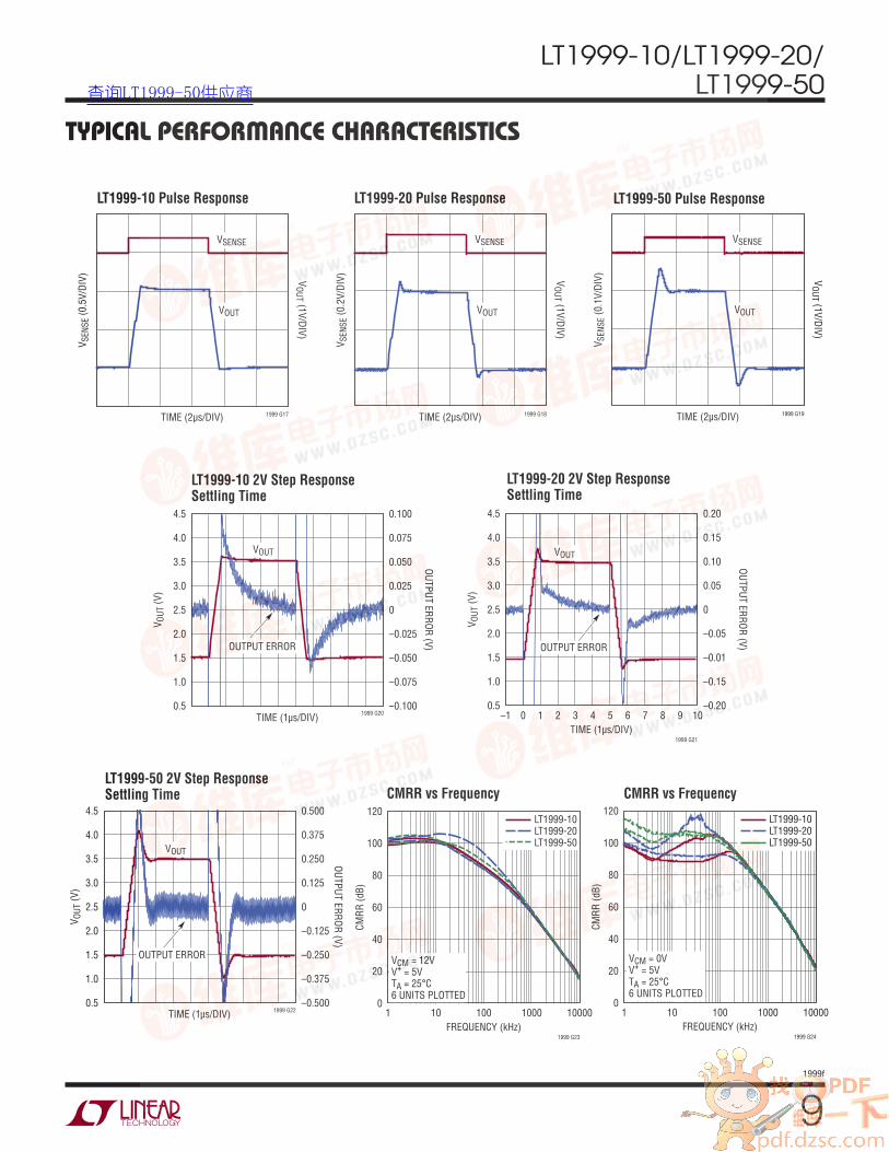
TYPICAL PERFORMANCE CHARACTERISTICS
Input Bias Current vs Input Common Mode Input Bias Current vs Temperature
Input Impedance vs Input Common Mode Voltage
VCM (V)
–5
I B (
mA
)
0.5
0
–1.0
–1.5
–0.5
–2.04525 65
1999 G07
75 8035155 55
V+ = 5V
TEMPERATURE (°C)
–55
I B (
μA
)
146
144
140
134
136
138
142
1327020 120
1999 G08
14545–5–30 95
VCM = 80V
VCM = 5.5V
VSHDN = OPENVINDIFF = 0VV+ = 5V
VCM (V)
–5
IMP
ED
AN
CE (
kΩ)
100000
10000
100
10
1000
14525 65
1999 G09
7535155 55
COMMON MODE INPUTIMPEDANCE
DIFFERENTIAL INPUT IMPEDANCE
Supply Current vs SHDN Pin Voltage
Shutdown Supply Currentvs Temperature
Shutdown Input Bias Current vs Input Common Mode
Supply Currentvs Input Common Mode Supply Current vs Temperature Supply Current vs Supply Voltage
VCM (V)
–5
I S (
mA
)
7
6
4
2
5
3
1
04525 65
1999 G01
75 8035155 55
V+ = 5V
TEMPERATURE (°C)
–55
I S (
mA
)
1.8
1.7
1.5
1.6
1.47020 120
1999 G02
14545–5–30 95
V+ = 5.5V
V+ = 4.5V
VSHDN = OPENVINDIFF = 0VVCM = 12V
SUPPLY VOLTAGE (V)
0
I S (
mA
)
4.0
3.0
1.0
2.0
3.5
1.5
2.5
0
0.5
2 4
1999 G03
51 3
VCM = 12V150°C130°C90°C25°C–45°C–55°C
VSHDN (V)
0
I S (
mA
)
10
0.1
1
0.001
0.01
2 4
1999 G04
51 3
TA = 25°C
TA = 150°C
TA = –55°C
V+ = 5VVCM = 12V
TEMPERATURE (°C)
–55
I S (
μA
)
10
8
4
2
6
07020 120
1999 G05
14545–5–30 95
V+ = 5.5V
V+ = 4.5V
VSHDN = 0VVINDIFF = 0VVCM = 12V
VCM (V)
0
I B (
nA
)
1000
10
100
140 80
1999 G06
10020 60
V+ = 5VVSHDN = 0VVSENSE = 0V
TA = 70°C
TA = 90°C
TA = 150°C
TA =110°C
TA =130°C
查询LT1999-50供应商

LT1999-10/LT1999-20/LT1999-50
81999f
TYPICAL PERFORMANCE CHARACTERISTICS
LT1999-10 Small Signal Frequency Response
Gain Error vs TemperatureGain Errorvs Input Common Mode Voltage
Input Referred Voltage Offset vs Temperature and Gain Option
Input Referred Voltage Offset vs Input Common Mode Voltage
TEMPERATURE (°C)
–55
VO
SI (μ
V)
1500
1000
–500
–1000
500
0
–15007020 120
1999 G10
14545–5–30 95
LT1999-10LT1999-20LT1999-50
VCM = 12V12 UNITS PLOTTED
VCM (V)
–5
VO
SI (μ
V)
1500
1000
–500
–1000
500
0
–15004525 65
1999 G11
7535155 55
V+ = 5VTA = 25°C12 UNITS PLOTTED
LT1999-10LT1999-20LT1999-50
TEMPERATURE (°C)
–55
GA
IN E
RR
OR
(%
)
0.50
0.25
–0.25
0
–0.507020 120
1999 G15
14545–5–30 95
VCM = 12V12 UNITS PLOTTED
LT1999-10LT1999-20LT1999-50
VCM (V)
–5
GA
IN E
RR
OR
(%
)
0.50
0.25
–0.25
0
–0.504525 65
1999 G16
7535155 55
V+ = 5VTA = 25°C12 UNITS PLOTTED
LT1999-10LT1999-20LT1999-50
FREQUENCY (kHz)
1
GA
IN (
dB
)
PH
AS
E (D
EG
)
30
15
0
–5
10
25
20
5
–10
180
45
–90
–135
0
135
90
–45
–18010 1000
1999 G12
10000100
VOUT = 0.5VP-P AT 1kHz
GAIN
PHASE
LT1999-50 Small Signal Frequency Response
LT1999-20 Small Signal Frequency Response
FREQUENCY (kHz)
1
GA
IN (
dB
)
PH
AS
E (D
EG
)
35
20
5
0
15
30
25
10
–5
180
45
–90
–135
0
135
90
–45
GAIN
–18010 1000
1999 G13
10000100
VOUT = 0.5VP-P AT 1kHz
PHASE
FREQUENCY (kHz)
1
GA
IN (
dB
)
PH
AS
E (D
EG
)
40
25
10
5
20
35
30
15
0
180
45
–90
–135
0
135
90
–45
GAIN
PHASE
–18010 1000
1999 G14
10000100
VOUT = 0.5VP-P AT 1kHz
查询LT1999-50供应商
LT1999-10/LT1999-20/LT1999-50
91999f
TYPICAL PERFORMANCE CHARACTERISTICS
CMRR vs FrequencyCMRR vs Frequency
FREQUENCY (kHz)
1
CM
RR
(dB
)
120
100
80
20
40
60
01000
1999 G23
1000010010
VCM = 12VV+ = 5VTA = 25°C6 UNITS PLOTTED
LT1999-10LT1999-20LT1999-50
LT1999-50 2V Step Response Settling Time
LT1999-10 2V Step Response Settling Time
LT1999-20 2V Step Response Settling Time
LT1999-50 Pulse Response
TIME (2μs/DIV)
VS
EN
SE (
0.1
V/D
IV) V
OU
T (1V
/DIV
)
1999 G19
VOUT
VSENSE
VOUT
TIME (1μs/DIV)
VO
UT (
V)
OU
TP
UT E
RR
OR
(V)
4.5
3.5
1.5
2.5
0.5
4.0
2.0
3.0
1.0
0.100
0.050
–0.050
0
–0.100
0.075
–0.025
0.025
–0.075
1999 G20
OUTPUT ERROR
VOUT
VO
UT (
V)
OU
TP
UT E
RR
OR
(V)
4.5
3.5
1.5
2.5
0.5
4.0
2.0
3.0
1.0
0.20
0.10
–0.01
0
–0.20
0.15
–0.05
0.05
–0.15
OUTPUT ERROR
TIME (1μs/DIV)
–1 42 6
1999 G21
7310 5 9 108
VO
UT (
V)
OU
TP
UT E
RR
OR
(V)
4.5
3.5
1.5
2.5
0.5
4.0
2.0
3.0
1.0
0.500
0.250
–0.250
0
–0.500
0.375
–0.125
0.125
–0.375
TIME (1μs/DIV)1999 G22
VOUT
OUTPUT ERROR
LT1999-10 Pulse Response LT1999-20 Pulse Response
TIME (2μs/DIV)
VS
EN
SE (
0.5
V/D
IV) V
OU
T (1V
/DIV
)
1999 G17
VOUT
VSENSE
TIME (2μs/DIV)
VS
EN
SE (
0.2
V/D
IV) V
OU
T (1V
/DIV
)
1999 G18
VOUT
VSENSE
FREQUENCY (kHz)
1
CM
RR
(dB
)
120
100
80
20
40
60
01000100
1999 G24
1000010
VCM = 0VV+ = 5VTA = 25°C6 UNITS PLOTTED
LT1999-10LT1999-20LT1999-50
查询LT1999-50供应商

LT1999-10/LT1999-20/LT1999-50
101999f
LT1999-10 Common Mode Rising Edge Step Response
VO
UT (
0.5
V/D
IV) V
CM
(25V
/DIV
)
TIME (0.5μs/DIV)1999 G25
VCM, tRISE ≈ 20ns
VOUT
LT1999-10 Common Mode Falling Edge Step Response
VO
UT (
0.5
V/D
IV) V
CM
(25V
/DIV
)
TIME (0.5μs/DIV)1999 G26
VCM, tFALL ≈ 20ns
VOUT
VO
UT (
0.5
V/D
IV) V
CM
(25V
/DIV
)
TIME (0.5μs/DIV)1999 G27
VCM, tRISE ≈ 20ns
VOUT
LT1999-20 Common Mode Rising Edge Step Response
LT1999-20 Common Mode Falling Edge Step Response
VO
UT (
0.5
V/D
IV) V
CM
(25V
/DIV
)
TIME (0.5μs/DIV)1999 G28
VCM, tFALL ≈ 20ns
VOUT
TYPICAL PERFORMANCE CHARACTERISTICS
LT1999-50 Common Mode Rising Edge Step Response
LT1999-50 Common Mode Falling Edge Step Response
VO
UT (
0.5
V/D
IV) V
CM
(25V
/DIV
)
TIME (0.5μs/DIV)1999 G29
VCM, tRISE ≈ 20ns
VOUT
VO
UT (
0.5
V/D
IV) V
CM
(25V
/DIV
)
TIME (0.5μs/DIV)1999 G30
VCM, tFALL ≈ 20ns
VOUT
查询LT1999-50供应商

LT1999-10/LT1999-20/LT1999-50
111999f
TYPICAL PERFORMANCE CHARACTERISTICS
LT1999 Input Referred Noise Density vs Frequency
FREQUENCY (kHz)
0.001 0.01 0.1
NO
ISE D
EN
SIT
Y (
nV
/√H
z)
1000
100
101000
1999 G31
10000101
TEMPERATURE (°C)
–55
I SC (
mA
)
40
20
30
10
–20
0
–40
–10
–30
7020 120
1999 G32
14545–5–30 95
SINKING
SOURCING
TEMPERATURE (°C)
–55
REF
PIN
VO
LTA
GE (
V)
3.0
2.5
1.0
2.0
0
1.5
0.5
7020 120
1999 G33
14545–5–30 95
SHDN MODE
ACTIVE MODE
V+ = 5V
Short-Circuit Current vs Temperature
REF Open Circuit Voltagevs Temperature
SHDN Pin Current vs SHDN Pin Voltage and Temperature
Turn-On/Turn-Off Time vs SHDN Voltage
VOUT vs VSENSE
I S (
1m
A/D
IV)
SH
DN
PIN
VO
LTAG
E (5
V/D
IV)
TIME (1μs/DIV)1999 G35
VSHDN
IS
SHUTDOWN
VCM = 12V
VSENSE (V)
–0.25
VO
UT (
V)
6
4
5
1
2
3
–1–0.05 0.15
1999 G36
0.25–0.15 0.05
VREF = 2.5V
LT1999-10LT1999-20LT1999-50
0
VSHDN (V)
0
I SH
DN
(μA
)
–2
–4
–1
0
–3
2 4 5
1999 G34
1 3
TA = 150°C
TA = 25°C
TA = –55°C
V+ = 5VVCM = 12V
VOUT vs VSENSE Over the Sense ABSMAX Range
VSENSE (V)
–60
VO
UT (
V)
6
4
5
1
2
3
–1–30 30
1999 G37
600
0
VOUT PHASE REVERSAL FOR VSENSE < –25V
VREF = 2.5V
LT1999-10LT1999-20LT1999-50
查询LT1999-50供应商

LT1999-10/LT1999-20/LT1999-50
121999f
PIN FUNCTIONSV+ (Pins 1, 4): Power Supply Voltage. Pins 1 and 4 are tied internally together. The specifi ed range of operation is 4.5V to 5.5V, but lower supply voltages (down to ap-proximately 4V) is possible although the LT1999 is not tested or characterized below 4.5V. See the Applications Information section.
+IN (Pin 2): Negative Sense Input Pin.
–IN (Pin 3): Positive Sense Input Pin.
GND (Pin 5): Ground Pin.
REF (Pin 6): Reference Pin Input. The REF pin sets the output common mode level and is set halfway between V+ and GND using a divider made of two 160k resis-tors. The default open circuit potential of the REF pin is mid-supply. It can be overdriven by an external voltage source cable of driving 80k to a mid-supply potential (see the Electrical Characteristics table for its specifi ed input voltage range).
OUT (Pin 7): Voltage Output. VOUT = AV•(VSENSE ± VOSI), where AV is the gain, and VOSI is the input referred offset voltage. The output amplifi er has a low impedance output and is designed to drive up to 200pF capacitive loads directly. Capacitive loads exceeding 200pF should be decoupled with an external resistor of at least 100Ω.
SHDN (Pin 8): Shutdown Pin. When pulled to within 0.5V of GND (Pin 5), will place the LT1999 into low power shutdown. If the pin is left fl oating, an internal 2μA pull-up current source will place the LT1999 into the active (amplifying) state.
查询LT1999-50供应商
LT1999-10/LT1999-20/LT1999-50
131999f
SHDN
V+
V+
D1
V+
V+
V+
V(G+IN)
V(G–IN)
2k
R+IN
R–IN
300Ω
CF4pF
0.8kR+S
0.8kR–S
160k
160k
1999 BD
2μA
OUT
REF
+IN
–IN
GND
+
–
+
–
GIN
RG
AO
2k
2k
4.5k
2k
8
72
1
3
4
6
5
BLOCK DIAGRAM
Figure 1. Simplified Block Diagram
TEST CIRCUIT
5V
5V
1999 F02
0.1μF
VOUT
VIN(DIFF)
+
–VCMVREF
VSHDN
+–
+–
+–
LT1999
4k
0.8k
160k
160k
2μA
0.8k4k
SHDN
V+
V+
V+
+
–
+
–
81
2
3
4
7
6
5
RG
0.1μF
V+
V+
Figure 2. Test Circuit
查询LT1999-50供应商

LT1999-10/LT1999-20/LT1999-50
141999f
The LT1999 current sense amplifi er provides accurate bidirectional monitoring of current through a user-selected sense resistor. The voltage generated by the current fl owing in the sense resistor is amplifi ed by a fi xed gain of 10V/V, 20V/V or 50V/V (LT1999-10, LT1999-20, or LT1999-50 respectively) and is level shifted to the OUT pin. The volt-age difference and polarity of the OUT pin with respect to REF (Pin 6) indicates magnitude and direction of the current in the sense resistor.
THEORY OF OPERATION
Refer to the Block Diagram (Figure 1).
Case 1: V+ < VCM < 80V
For input common mode voltages exceeding the power supply, one can assume D1 of Figure 1 is completely off. The sensed voltage (VSENSE) is applied across Pin 2 (+IN) and Pin 3 (–IN) to matched resistors R+IN and R–IN (nomi-nally 4k each). The opposite ends of R+IN and R–IN are forced to equal potentials by transconductor GIN, which convert the differentially sensed voltage into a sensed current. The sensed current in R+IN and R–IN is combined, level-shifted, and converted back into a voltage by trans-resistance amplifi er AO and resistor RG. Amplifi er AO provides high open loop gain to accurately convert the sensed current back into a voltage and to drive external loads. The theoretical output voltage is determined by the sensed voltage (VSENSE), and the ratio of two on-chip resistors:
VOUT − VREF = VSENSE •
RGRIN
where
RIN =
R+IN + R−IN2
nominally 4k
For the LT1999-10, RG is nominally 40k. For the LT1999-20, RG is nominally 80k, and for the LT1999-50, RG is nomi-nally 200k.
APPLICATIONS INFORMATIONThe voltage difference between the OUT pin and the REF pin represent both polarity and magnitude of the sensed voltage. The noninverting input of amplifi er AO is biased by a resistive 160k to 160k divider tied between V+ and GND to set the default REF pin bias to mid-supply.
Case 2: –5V < VCM < V+
For common mode inputs which transition or are set below the supply voltage, diode D1 will turn on and will provide a source of current through R+S and R–S to bias the inputs of transconductance amplifi er GIN at least 2.25V above GND. The transition is smooth and continuous; there are negligible changes to either gain or amplifi er voltage offset. The only difference in amplifi er operation is the bias currents provided by D1 through R+S and R–S are steered through the input pins, otherwise amplifi er operation is identical. The inputs to transconductance amplifi er GIN are still forced to equal potentials forcing any differential voltages appearing at the +IN and –IN pins into a differential current. This differential current is combined, level-shifted, and converted back into a voltage by trans-resistance amplifi er AO and Resistor RG. Resistors R+S and R–S are trimmed to match R+IN and R–IN respectively, to prevent common mode to differential conversion from occurring (to the extent of the matched trim) when the input common mode transitions below V+.
As described in case 1, the output is determined by the sense voltage and the ratio of two on-chip resistors:
VOUT − VREF = VSENSE •
RGRIN
where
RIN =
R+IN + R−IN2
查询LT1999-50供应商

LT1999-10/LT1999-20/LT1999-50
151999f
APPLICATIONS INFORMATIONInput Common Mode Range
The LT1999 was optimized for high common mode re-jection. Its input stage is balanced and fully differential, designed to amplify differential signals and reject common mode signals. There is negligible crossover distortion due to sense voltage reversals. The amplifi er is most linear in the zero-sense region.
With the V+ supply confi gured within the specifi ed and tested range (4.5V < V+ < 5.5V), the LT1999’s common mode range extends from –5V to 80V. Pushing +IN and –IN beyond the limits specifi ed in the Absolute Maximum table can turn on the voltage clamps designed to protect the +IN and –IN pins during ESD events.
It is possible to operate the LT1999 on power supplies as low as 4V (although it is not tested or specifi ed below 4.5V). Operating the LT1999 on supplies below 4V will produce erratic behavior. When operating the LT1999 with supplies as low as 4V, the common mode range for inputs which extend below GND is reduced. Refer to the Block Diagram (Figure 1). For inputs driven below V+, diode D1 conducts. For proper operation, the input to the transconductor V(G+IN) must be biased at approximately 2.25V above the GND pin. V(G+IN) sits on the centertap of a voltage divider comprised of R+S and R+IN V(G–IN) likewise sits in the middle of the voltage divider comprised of R–S , and R–IN). The voltage on V(G+IN) input is given by the following equation:
V(G+IN) = V +IN•
R +SR +S + R+IN
+ V+ −VD1( ) •R +IN
R +S + R+IN
Setting V(G+IN) = 2.25V, the ratio (R+IN/R+S) to 5, and VD1 equal to 0.8V (cold temperatures), a plot of the lower input common mode range plotted against supply is shown in Figure 3.
Output Common Mode Range
The LT1999’s output common mode level is set by the voltage on the REF pin. The REF pin sits in the middle of a 160k to 160k voltage divider connected between V+ and GND which sets the default open circuit potential of the REF pin to mid-supply. It can be overdriven by an external voltage source capable of driving 80k tied to a mid-supply potential. See the Electrical Characteristics table for the REF pin’s specifi ed input voltage range.
Differential sampling of the OUT pin with respect the REF pin provides the best noise immunity. Measurements of the output voltage made differentially with respect to the REF pin will provide the highest power supply and com-mon mode rejection. Otherwise, power supply or GND pin disturbances are divided by the REF pin’s voltage divider and appear directly at the noninverting input of the trans-resistance amplifi er AO and are not rejected.
If not driven by a low impedance (<100Ω), the REF pin should be fi ltered with at least 1nF of capacitance to a low impedance, low noise ground plane. This external capacitance will also provide a charge reservoir during high frequency sampling of the REF pin by ADC inputs attached to this pin.
Figure 3. Lower Input Common Mode vs Supply Voltage
SUPPLY VOLTAGE (V)
4
VC
M(L
OW
ER
LIM
IT)
(V)
–2.0
–2.5
–3.0
–4.0
–5.0
–3.5
–4.5
–5.5
–6.04.754.25 5.25
1999 F03
5.54.5 5
BELOW GROUND INPUTCOMMON MODE RANGELIMITED BY V+ SUPPLY VOLTAGE
BELOW GROUND INPUTCOMMON MODE RANGELIMITED BY ESD CLAMPS
TYPICAL ESD CLAMP VOLTAGE
查询LT1999-50供应商

LT1999-10/LT1999-20/LT1999-50
161999f
APPLICATIONS INFORMATIONShutdown Capability
If SHDN (Pin 8) is driven to within 0.5V of GND, the LT1999 is placed into a low power shutdown state in which the part will draw about 3μA from the V+ supply. The input pins (+IN and –IN) will draw approximately 1nA if biased within the range of 0V to 80V (with no differential voltage applied). If the input pins are pulled below the GND pin, each input appears as a diode tied to GND in series with approximately 4k of resistance. The REF pin appears as approximately 0.4MΩ tied to a mid-supply potential. The output appears as reverse biased diodes tied between the output to either V+ or GND pins.
EMI Filtering and Layout Practices
An internal 1st order differential lowpass noise/EMI sup-pression fi lter with a –3dB bandwidth of 10MHz (approxi-mately 5× the LT1999’s –3dB bandwidth) is included to help improve the LT1999’s EMI susceptibility and to assist with the rejection of high frequency signals beyond the
bandwidth of the LT1999 that may introduce errors. The pole is set by the following equation:
ffi lt = 1/(π•(R+IN + R–IN)•CF) ≈ 10MHz
Both the resistors and capacitors have a ±15% variation so the pole can vary by approximately ±30% over manu-facturing process and temperature variations.
The layout for lowest EMI/noise susceptibility is achieved by keeping short direct connections and minimizing loop areas (see Figure 4). If the user-supplied sense resistor cannot be placed in close proximity to the LT1999, the surface area of the loop comprising connections of +IN to RSENSE and back to –IN should be minimized. This re-quires routing PCB traces connecting +IN to RSENSE and –IN to RSENSE adjacent with one another with minimal separation. The metal traces connecting +IN to the sense resistor and –IN to the sense resistor should match and use the same trace width.
Bypassing the V+ pin to the GND pin with a 0.1μF capacitor with short wiring connection is recommended.
Figure 4. Recommended Layout
SUPPLY BYPASSCAPACITOR
* KEEP LOOP AREA COMPRISING RSENSE, +IN AND –IN PINS AS SMALL AS POSSIBLE.** REF BYPASS TIED TO A LOW NOISE, LOW IMPEDANCE SIGNAL GROUND PLANE.† OPTIONAL 10pF CAPACITOR TO PREVENT dV/dt EDGES ON INPUT COUPLING TO FLOATING SHDN PIN.
**
*
FROM DC SOURCE
TO LOAD
RSENSEDIFFERENTIALANALOG OUT
†
1999 F03
1
2
3
4
8
7
6
5
SHDN
OUT
REF
GND
V+
+IN
–IN
V+
查询LT1999-50供应商

LT1999-10/LT1999-20/LT1999-50
171999f
APPLICATIONS INFORMATIONThe REF pin should be either driven by a low source im-pedance (<100Ω) or should be bypassed with at least 1nF to a low impedance, low noise, signal ground plane (see Figure 4). Larger bypass capacitors on both V+ pins, and the REF pin, will extend enhanced AC CMRR, and PSRR performance to lower frequencies. Bypassing the REF pin to a quiet ground plane fi lters the V+ pin or GND pin noise that is sensed by the REF pin voltage divider and applied to the noninverting input of output amplifi er AO. Any com-mon I•R drops generated by pulsating ground currents in common with the REF pin fi lter capacitor can compromise the fi ltering performance and should be avoided.
If the SHDN pin is not driven and is left fl oating, routing a PCB trace connecting Pins 1 and 8 under the part will act as a shield, and will help limit edge coupling from the inputs (Pins 2 and 3) to the SHDN pin. Periodic pulses on the inputs with fast edges may glitch the high impedance SHDN pin, periodically putting the part into low power shutdown. Additional precaution against this may be taken by adding an optional small (~10pF) capacitor may be tied between V+ (Pin 1) and Pin 8.
Finally, when connecting the LT1999 inputs to the sense resistor, it is important to use good Kelvin sensing practices (sensing the resistor in a way that excludes PCB trace I•R voltage drops). For sense resistors less than 1Ω, one might consider using a 4-wire sense resistor to sense the resistive element accurately.
Selection of the Current Sense Resistor
The external sense resistor selection presents a delicate trade-off between power dissipation in the resistor and current measurement accuracy.
In high current applications, the user may want to mini-mize the power dissipated in the sense resistor. The sense resistor current will create heat and voltage loss, degrading effi ciency. As a result, the sense resistor should be as small as possible while still providing adequate dynamic range required by the measurement. The dynamic range is the ratio between the maximum accurately produced signal generated by the voltage across the sense resistor, and the minimum accurately reproduced signal. The minimum accurately reproduced signal is primarily dictated by the voltage offset of the LT1999. The maximum accurately reproduced signal is dictated by the output swing of the LT1999.
Thus the dynamic range for the LT1999 can be thought of the maximum sense voltage divided by the input referred voltage offset or:
Dynamic Range =
ΔVOUT(MAX)
GAIN • VOSI
The above equation tells us that the dynamic range is inversely proportional to the gain of the LT1999. Thus, if accuracy is of greater importance than effi ciency or power loss, the LT1999-10 used with the highest valued sense resistor possible is recommended. If effi ciency, heat generated, and power loss in the resistive shunt is the primary concern, the LT1999-50 and the lowest value sense resistor possible is recommended. The LT1999-20 is available for applications somewhere in between these two extremes.
查询LT1999-50供应商

LT1999-10/LT1999-20/LT1999-50
181999f
APPLICATIONS INFORMATION
VOUT
VREF
VSHDN
LT1999
4k
0.8k
160k
160k
2μA
0.8k4k
SHDN
V+
V+
V+
+
–
+
–
81
2
3
4
7
6
5
RG
V+
V+VS
5V
1999 F05
0.1μF
0.1μF
FUSE
STEERINGDIODELOAD
ILOAD
RSENSE
OFFON
5V
VOUT
V+IN
V–IN VREF
VSHDN
Figure 5. Using the LT1999 to Monitor a Fuse
Fuse Monitor
The inputs can be overdriven without fear of damaging the LT1999. This makes the LT1999 ideal for monitoring fuses if either +IN or –IN are shorted to ground while the other is at the full common mode supply voltage (see Figure 5). If the fuse in Figure 5 opens with the +IN tied to the positive supply, the load will pull –IN to GND. The output will be forced to the positive V+ supply rail. If it is desired that the output be near ground if the fuse opens, it is a simple matter of swapping the inputs. Precautions should be followed: First, when the inputs are stressed differentially due to the fuse blowing open, a large voltage drop will be placed across the +IN to –IN pins, dissipating
power in the precision on-chip input resistors. Precaution should be taken to prevent junction temperatures from exceeding the Absolute Maximum ratings (see Note 3 in the Electrical Characteristics section). Secondly, if the load is inductive, and the fuse blows open without a clamp diode, energy stored in the inductive load will be dissipated in the LT1999, which could cause damage. A simple steering diode as shown in Figure 5 will prevent this from happen-ing, and will protect the LT1999 from damage.
Finally, the user should be aware that in fuse monitoring applications with the sense voltage (VSENSE = V+IN – V–IN) being driven in excess of –25V, the output of the LT1999 will undergo phase reversal (see Figure 6).
Figure 6. A Plot of the LT1999’s Output Voltage vs VSENSE (VSENSE = V+IN – V–IN). In Applications Where the Sense Voltage Is Driven in Excess of –25V, the Output of the LT1999 Will Undergo Phase Reversal
VSENSE (V)
–60
VO
UT (
1V
/DIV
)
–30–45 –15 30
1999 F06
6015 450
VOUT PHASE REVERSAL FOR VSENSE < –25V
VREF = 2.5V
查询LT1999-50供应商

LT1999-10/LT1999-20/LT1999-50
191999f
TYPICAL APPLICATIONSSolenoid Current Monitor
The solenoid of Figure 7 consists of a coil of wire in an iron case with permeable plunger that acts as a movable element. When the MOSFET turns on, the diode is reversed biased off, and current fl ows through RSENSE to actuate the solenoid. If the MOSFET is turned off, the current in the MOSFET is interrupted, but the energy stored in the solenoid causes the diode to turn on and current to freewheel in the loop consisting of the diode, RSENSE and the solenoid.
Figure 7 shows the LT1999 monitoring currents in a ground referenced solenoid used when the coil is hard tied to the case, and is tied to ground. Figure 8 shows a supply referenced solenoid whose coil is insulated from the case. The LT1999 will interface equally well to either of these two confi gurations.
Bidirectional PWM Motor Monitor
Pulse width modulation is commonly used to effi ciently vary the average voltage applied across a DC motor. The H-bridge topology of Figure 9 allows full 4-quadrant control: clockwise control, counter-clockwise control, clockwise regeneration, and counter-clockwise regeneration. The LT1999 in conjunction with a non-inductive current shunt is used to monitor currents in the rotor. The LT1999 can be used to detect stuck rotors, provide detection of over-current conditions in general, or provide current mode feedback control.
Figure 10 shows a plot of the output voltage of the LT1999.
Figure 7. Solenoid Current Monitor for Ground Tied Solenoid. The Common Mode Inputs to the LT1999 Switch Between VS and One Diode Drop Below Ground
LT1999
4k
0.8k
160k
160k
2μA
0.8k4k
SHDN
V+
V+
V+
+
–
+
–
81
2
3
4
7
6
5
RG
V+
V+
TIME (50ms/DIV)
VO
UT (
0.5
V/D
IV) V
+IN
(10V
/DIV
)
5V
VS
5V
1999 F07a
1999 F07b
0.1μF
0.1μF
SOLENOID
RSENSE
V+IN
VSHDN
VOUT
VREFV–IN
ON
OFF
VOUT
V+IN
SOLENOID PLUNGER PULLS IN
SOLENOID RELEASES
2.5V
查询LT1999-50供应商

LT1999-10/LT1999-20/LT1999-50
201999f
Figure 8. Solenoid Current Monitor for Non-Grounded Solenoids. This Circuit Performs the Same Function as Figure 7 Except One End of the Solenoid Is Tied to VS. The Common Mode Voltage of Inputs of the LT1999 Switch Between Ground and One Diode Drop Above VS
TYPICAL APPLICATIONS
LT1999
4k
0.8k
160k
160k
2μA
0.8k4k
SHDN
V+
+
–
+
–
8
2
3
7
6
5
RG
V+
V+
5V
VS
5V
1999 F08a
1
40.1μF
2.5V
0.1μF
SOLENOID
RSENSE
VOUT
VREF
VSHDN
ON
OFFV+
V+
V+IN
V–IN
TIME (50ms/DIV)
VO
UT (
0.5
V/D
IV) V
+IN
(10V
/DIV
)
VOUT
V+IN
SOLENOID PLUNGER PULLS IN
SOLENOID RELEASES
1999 F08b
查询LT1999-50供应商

LT1999-10/LT1999-20/LT1999-50
211999f
TYPICAL APPLICATIONS
Figure 9. Armature Current Monitor for DC Motor Applications
Figure 10. LT1999 Output Waveforms for the Circuit of Figure 9
1999 F09
VBRIDGE
V+IN
V–IN
RSENSE0.025Ω
10μF
PWM INPUT
DIRECTION
BRAKE INPUT
24V
5V
5V
GND
5V
PWM INOUTA
OUTB
C41000μF
24V MOTOR
H-BRIDGE
LT1999-20
4k
0.8k
160k
160k
2μA
0.8k4k
SHDN
+
–
+
–
80k
V+
V+V+
V+0.1μF
0.1μF
8
7
6
VSHDN
VOUT
VREF
2
3
1
4
V+
5
TIME (20μs/DIV)
VO
UT (
2V
/DIV
) V+IN
(20V
/DIV
)
1999 F10
VOUT
V+IN
2.5V
查询LT1999-50供应商

LT1999-10/LT1999-20/LT1999-50
221999f
PACKAGE DESCRIPTIONMS8 Package
8-Lead Plastic MSOP(Reference LTC DWG # 05-08-1660 Rev F)
MSOP (MS8) 0307 REV F
0.53 ± 0.152
(.021 ± .006)
SEATINGPLANE
NOTE:1. DIMENSIONS IN MILLIMETER/(INCH)2. DRAWING NOT TO SCALE3. DIMENSION DOES NOT INCLUDE MOLD FLASH, PROTRUSIONS OR GATE BURRS. MOLD FLASH, PROTRUSIONS OR GATE BURRS SHALL NOT EXCEED 0.152mm (.006") PER SIDE4. DIMENSION DOES NOT INCLUDE INTERLEAD FLASH OR PROTRUSIONS. INTERLEAD FLASH OR PROTRUSIONS SHALL NOT EXCEED 0.152mm (.006") PER SIDE5. LEAD COPLANARITY (BOTTOM OF LEADS AFTER FORMING) SHALL BE 0.102mm (.004") MAX
0.18
(.007)
0.254
(.010)
1.10
(.043)MAX
0.22 – 0.38
(.009 – .015)TYP
0.1016 ± 0.0508
(.004 ± .002)
0.86
(.034)REF
0.65
(.0256)BSC
0° – 6° TYP
DETAIL “A”
DETAIL “A”
GAUGE PLANE
1 2 3 4
4.90 ± 0.152
(.193 ± .006)
8 7 6 5
3.00 ± 0.102
(.118 ± .004)
(NOTE 3)
3.00 ± 0.102
(.118 ± .004)
(NOTE 4)
0.52
(.0205)REF
5.23(.206)MIN
3.20 – 3.45(.126 – .136)
0.889 ± 0.127(.035 ± .005)
RECOMMENDED SOLDER PAD LAYOUT
0.42 ± 0.038(.0165 ± .0015)
TYP
0.65(.0256)
BSC
查询LT1999-50供应商

LT1999-10/LT1999-20/LT1999-50
231999f
Information furnished by Linear Technology Corporation is believed to be accurate and reliable. However, no responsibility is assumed for its use. Linear Technology Corporation makes no representa-tion that the interconnection of its circuits as described herein will not infringe on existing patent rights.
PACKAGE DESCRIPTIONS8 Package
8-Lead Plastic Small Outline (Narrow .150 Inch)(Reference LTC DWG # 05-08-1610)
.016 – .050(0.406 – 1.270)
.010 – .020(0.254 – 0.508)
× 45°�
0°– 8° TYP.008 – .010
(0.203 – 0.254)
SO8 0303
.053 – .069(1.346 – 1.752)
.014 – .019(0.355 – 0.483)
TYP
.004 – .010(0.101 – 0.254)
.050(1.270)
BSC
1 2 3 4
.150 – .157(3.810 – 3.988)
NOTE 3
8 7 6 5
.189 – .197(4.801 – 5.004)
NOTE 3
.228 – .244(5.791 – 6.197)
.245MIN .160 ±.005
RECOMMENDED SOLDER PAD LAYOUT
.045 ±.005 .050 BSC
.030 ±.005 TYP
INCHES(MILLIMETERS)
NOTE:1. DIMENSIONS IN
2. DRAWING NOT TO SCALE3. THESE DIMENSIONS DO NOT INCLUDE MOLD FLASH OR PROTRUSIONS. MOLD FLASH OR PROTRUSIONS SHALL NOT EXCEED .006" (0.15mm)
查询LT1999-50供应商
LT1999-10/LT1999-20/LT1999-50
241999f
Linear Technology Corporation1630 McCarthy Blvd., Milpitas, CA 95035-7417 (408) 432-1900 ● FAX: (408) 434-0507 ● www.linear.com © LINEAR TECHNOLOGY CORPORATION 2010
LT 1110 • PRINTED IN USA
TYPICAL APPLICATION
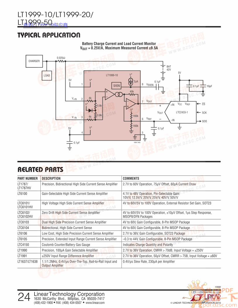
PART NUMBER DESCRIPTION COMMENTS
LT1787/LT1787HV
Precision, Bidirectional High Side Current Sense Amplifier 2.7V to 60V Operation, 75μV Offset, 60μA Current Draw
LT6100 Gain-Selectable High Side Current Sense Amplifier 4.1V to 48V Operation, Pin-Selectable Gain: 10V/V, 12.5V/V, 20V/V, 25V/V, 40V/V, 50V/V
LTC6101/LTC6101HV
High Voltage High Side Current Sense Amplifier 4V to 60V/5V to 100V Operation, External Resistor Set Gain, SOT23
LTC6102/LTC6102HV
Zero Drift High Side Current Sense Amplifier 4V to 60V/5V to 100V Operation, ±10μV Offset, 1μs Step Response, MSOP8/DFN Packages
LTC6103 Dual High Side Precision Current Sense Amplifier 4V to 60V, Gain Configurable, 8-Pin MSOP Package
LTC6104 Bidirectional, High Side Current Sense 4V to 60V, Gain Configurable, 8-Pin MSOP Package
LT6106 Low Cost, High Side Precision Current Sense Amplifier 2.7V to 36V, Gain Configurable, SOT23 Package
LT6105 Precision, Extended Input Range Current Sense Amplifier –0.3 to 44V, Gain Configurable, 8-Pin MSOP Package
LTC4150 Coulomb Counter/Battery Gas Gauge Indicates Charge Quantity and Polarity
LT1990 Precision, 100μA Gain Selectable Amplifier 2.7V to 36V Operation, CMRR > 70dB, Input Voltage = ±250V
LT1991 ±250V Input Range Difference Amplifier 2.7V to 36V Operation, 50μV Offset, CMRR > 75B, Input Voltage = ±60V
LT1637/LT1638 1.1/1.2MHz, 0.4V/μs Over-The-Top, Rail-to-Rail Input and Output Amplifier
0.4V/μs Slew Rate, 230μA per Amplifier
RELATED PARTS
1999 TA02
5V0.1μF
LT1999-10
4k
0.8k
160k
160k
2μA
0.8k4k
V+
+
–
SHDN
+
–VOUT
40k
VREF
VSHDN
V+
V+
V+
V+
4
0.1μF
5V
CHARGER
LOAD
0.025Ω
BAT42V
VCC VREF
0.1μF
+IN
10μF
CS
SCK
SDO
LTC2433-1VOUT
+
–
5V
–IN
0.1μF
2
3
1
5
7
6
8
V+IN
V–IN
Battery Charge Current and Load Current MonitorVOUT = 0.25V/A, Maximum Measured Current ±9.5A
查询LT1999-50供应商