low power design implementation and verification
TRANSCRIPT

LOW POWER DESIGN IMPLEMENTATION AND VERIFICATION
A Project
Presented to the faculty of the Department of Electrical and Electronic Engineering
California State University, Sacramento
Submitted in partial satisfaction of
the requirements for the degree of
MASTER OF SCIENCE
in
Electrical and Electronic Engineering
by
Tejas Hadke
FALL
2014

ii
© 2014
Tejas Hadke
ALL RIGHTS RESERVED

iii
LOW POWER DESIGN IMPLEMENTATION AND VERIFICATION
A Project
by
Tejas Hadke
Approved by:
__________________________________, Committee Chair
Dr. Behnam Arad
__________________________________, Second Reader
Dr. Nikrouz Faroughi
____________________________
Date

iv
Student: Tejas Hadke
I certify that this student has met the requirements for format contained in the University format
manual, and that this project is suitable for shelving in the Library and credit is to be awarded for
the project.
__________________________, Graduate Coordinator ___________________
Dr. Preetham Kumar Date
Department of Electrical and Electronic Engineering

v
Abstract
of
LOW POWER DESIGN IMPLEMENTATION AND VERIFICATION
by
Tejas Hadke
According to Moore’s law, the number of transistors on integrated circuits (ICs) double
approximately every two years. Over the years, this growth in number of transistors has reached
to billions of transistors per IC, operating at very high frequencies. However, there are many
factors limiting this growth rate including power consumption of high-density high-speed
integrated circuits. Various techniques have evolved offering reduction in dynamic power
consumption and leakage power. Traditional methods like use of power efficient circuits,
parallelism in micro-architectures, along with nontraditional methods such as clock gating,
variable supply voltage and frequency scaling are becoming significantly important in lowering
dynamic power consumption. The leakage power, which has become more significant in the
recent high-density designs, can be reduced by minimizing usage of low threshold voltage cells,
adding power gating, back biasing, reducing oxide thickness, and using new devices such as
FINFET’s. Design engineers have to consider clock and power gating techniques up front in the
design cycle in today’s multi-threshold, multi-oxide, multi-voltage and multi-clock devices.
Understanding and implementing power intent at register transfer level (RTL), netlist and PG
netlist stages requires additional design verification efforts.

vi
In this project, several power reduction and management techniques were studied and applied to
an existing System on Chip (SoC) system consisting of an ARM processor, an Ethernet
controller, and a DDR controller. Clock and Multi VDD power gating were considered as
primary techniques for achieving power reduction. Power intent was created as per the IEEE
1801-2009 Unified Power Format standard. Open source Verilog model of the SoC ARM
processor was used as a reference model, along with Synopsys® 90 nm cell library. Synopsys®
Electronic Design Automation (EDA) tools were utilized in carrying out simulation, synthesis,
and power analysis phases of the project.
In addition to implementation of low-power RTL design techniques, use of clock gating, power
gating, multi-voltage design partition and multi-threshold voltage cells showed significant
improvement in power consumption of the System on Chip (SoC) system used in this work. By
considering design issues and verification requirements of these techniques, we developed a
power-aware SoC design flow. This enhanced methodology presents a unique approach for
effectively incorporating low-power techniques early in the design phase.
_______________________, Committee Chair
Dr. Behnam Arad
_______________________
Date

vii
ACKNOWLEDGEMENTS
I would like to express my gratitude to my advisors, Dr. Behnam Arad for guiding this work with
utmost interest, care and patience. I am grateful to them for introducing me to the subject of low
power design and giving me the freedom to explore my ideas. I would like to thank Dr. Nikrouz
Faroughi for finding the time to serve on my master’s project committee and providing his
valuable feedback. I also thank them for teaching excellent courses on Computer Architecture and
Hierarchical Digital Design that laid the foundation for my project work. I would like to
I extend my thanks Dr. Perry Heedley for explaining latest developments in device level low
power design techniques and sharing information. A special thanks to Mike Wimple and Ray
Fraizer for helping EDA and logistic issues. My sincere thanks also goes to my graduate
coordinator, Dr. Preetham Kumar and Department of Electrical and Electronics Engineering, for
all the help and opportunities I received to pursue master of science program at California state
university. Sacramento.
I owe a special gratitude to my parents Mr. Ashok Hadke and Mrs. Manik Hadke and my brother,
Amit Hadke, for supporting and motivating me during my two years of tough academic times.
Finally, I would like to express my gratitude to my friends Anhad Singh who helped me in
formatting this work; Pramod Gavade and Devesh Binjola for the support they provided me
during the last few days of the project work.

viii
TABLE OF CONTENTS
Acknowledgements ........................................................................................................................ vii
List of Tables ................................................................................................................................... x
List of Figures ................................................................................................................................. xi
Chapter
1. INTRODUCTION ....................................................................................................................... 1
2. BACKGROUND AND RELATED WORK ............................................................................... 3
2.1 Fundamentals of power consumption in CMOS ....................................................... 3
2.2 Architectural level (RTL) power reduction techniques ............................................. 5
2.3 Clock Gating ......................................................................................................... 7
2.3.1 Architectural clock gating technique ....................................................... 8
2.3.2 Gate level clock gating .......................................................................... 9
2.4 Frequency scaling, dynamic voltage scaling .......................................................... 11
2.5 Use of multi threshold voltage cells ...................................................................... 12
2.6 Use of multi VDD and power gating ..................................................................... 13
3. POWER AWARE DESIGN IMPLEMENTATION .................................................................. 18
3.1 Background of resources ...................................................................................... 18
3.1.1 Amber SoC system .............................................................................. 18
3.1.2 Synopsys 90nm Library ....................................................................... 20
3.1.3 Typical ASIC Front end design flow ..................................................... 20
3.2 Power aware technique implementation ................................................................ 22
3.2.1 Power aware implementation flow ........................................................ 22

ix
3.2.2 Power aware RTL modifications .......................................................... 25
3.2.2 Clock Gating ....................................................................................... 25
3.2.3 Frequency Scaling ............................................................................... 27
3.2.4 Use of HVT/LVT voltage cells ............................................................. 28
3.2.5 Multi VDD design ............................................................................... 28
3.3 Power Estimation and Verification ....................................................................... 34
3.3.1 Multi Voltage (MV) static verification .................................................. 34
3.3.2 Power Estimation ................................................................................ 34
4. RESULTS AND DISCUSSIONS .............................................................................................. 36
4.1 Results of low power implementations .................................................................. 36
5. CONCLUSION .......................................................................................................................... 40
Appendix A. Power aware RTL modifications .............................................................................. 42
Appendix B. Design Implementation scripts, Reports, Violations ................................................ 50
Appendix C. Examples and Key commands .................................................................................. 63
Appendix D. Glossary .................................................................................................................... 66
References ...................................................................................................................................... 67
x
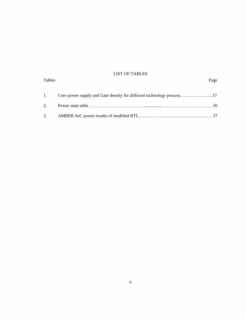
LIST OF TABLES
Tables Page
1. Core power supply and Gate density for different technology process………………….17
2. Power state table …………………………….… ................. ……………………………30
3. AMBER SoC power results of modified RTL………… . ………….……………………37

xi
LIST OF FIGURES
Figures Page
1. Short Circuit Current Path in CMOS inverter ……. .……………………………….4
2. Clock Gating on clock domain ………………….…………………………………….8
3. Multiple levels of clock gating logic ………. ………….……………………………9
4. Fine grain clock gating inserted during synthesis..…..…………………………......10
5. Frequency scaling example ……………………………………………….……...11
6. Level shifter cell application ......................................................................….......14
7. Isolation cell usage ……………...…………….……..…………………………......15
8. Retention cells ...........................................................................................…........15
9. Typical Multi VDD Synthesis flow……………………………………….…......17
10. AMBER FPGA System………………………………………………………......19
11. Typical frontend design flow………………………………………..………….....21
12. Power Aware design flow……………………………….………..…………….....24
13. Frequency scaling block added to AMBER SoC………………………………..27
14. Power domain/UPF diagram of AMBER SoC…………………………………..32
15. Block diagram of AMBER SoC as per power domain ……………………….....33
16. Modified Amber SoC -Dynamic power reduction results…………….………….37
17. Modified Amber SoC Leakage power reduction …….………………………….. 38
18. Modified Amber SoC Total power reduction………………………………….…39

ii

1
CHAPTER 1: INTRODUCTION
According to Moore’s law, number of transistors on integrated circuits doubles approximately
every two years. Over the years, this growth in number of transistors has reached to billions of
transistors, operating at very high frequencies. However, there are many factors limiting this rate.
One of the serious impediment to this growth is the power consumption of high-density high-
speed integrated circuits. Due to process scaling, leakage power is significantly increasing below
sub threshold technologies. Higher density of transistors increases power consumption of the
device. Modern day industry/market adoption of mobile applications has created a need for more
power efficient devices. Cellular phones, digital cameras, hand held gaming and media playing
devices, and wireless devices need to be high-performance and power efficient. Power
consumption by these devices has become a major performance metric along with their speed.
Variety of techniques evolved over the years that offer reduction in dynamic power consumption
and leakage power. Along with traditional methods like use of power efficient circuits, design
engineers have started using clock-gating, variable supply voltage and frequency, parallelism vs
high frequency approach, to reduce dynamic power. The leakage power, which has become
significant in the recent high-density designs can be reduced by minimizing usage of low
threshold voltage cells, adding power gating, back biasing, reducing oxide thickness, using new
devices such as FINFET’s.
This project discusses the constructive study of these power reduction techniques and focuses on
the implementation of these design techniques on a reference System on Chip (SoC) design. The
clock and power gating are considered as primary techniques for achieving power reduction. The
power intent is created as per the IEEE 1801-2009 Unified Power Format standard. Verilog

2
model for an open source, ARM-compatible, 32-bit RISC processor [5] is used as a reference
model to start, along with Synopsys 90nm technology library and tools for carrying out
simulation, synthesis, power estimation. The scope of this project is limited to applying the
studied techniques from the front-end VLSI design engineer’s point of view. Constructive
analysis of power estimation results, efforts required for design and verification were used as
guidelines to generalize best-known methods and flow for the low power design methodology.
This report is organized as follows –
Chapter 1: Introduction - This introduces the project work and goal of the project in brief.
Chapter 2: Background and Related Work - This chapter gives an introduction of why power
aware design techniques are becoming important and introduces a related design methodologies
used.
Chapter 3: Power aware design implementation - In this chapter, practical approach used to
implement low power design techniques for this project is explored in details.
Chapter 4: Results - This chapter discusses findings and interpretations of the results obtained
from the power aware design changes. It also brings up common issues, design and verification
efforts required to implement these techniques and best-known methods.
Chapter 5: Conclusion - This chapter summarizes the project report and the findings made. It also
presents the conclusion to this project.
Appendix A: Power aware RTL modifications
Appendix B: Design Implementation scripts, Reports, Violations
Appendix C: Examples and Key commands
Appendix D: Glossary
References

3
CHAPTER 2: BACKGROUND AND RELATED WORK
This following part of the introduction provides a background of these power reduction
techniques.
1. Fundamentals of power consumption in CMOS
2. RTL level power reduction techniques
3. Clock Gating
4. Frequency scaling, dynamic voltage scaling
5. Use of multi threshold voltage cells
6. Power Gating and Multi Voltage design
2.1 Fundamentals of power consumption in CMOS
There are three key factors that contribute to power consumption in CMOS circuits –
1. Switching Power
2. Short Circuit Power or Internal Power
3. Leakage Power
Switching power in CMOS based circuits is due to charging and discharging of load capacitances
or equivalent output capacitances. Energy and power equations are below –
𝐸𝑛𝑒𝑟𝑔𝑦 𝑝𝑒𝑟 𝑡𝑟𝑎𝑛𝑠𝑖𝑡𝑖𝑜𝑛𝑠 = 𝐶𝐿 × 𝑉𝐷𝐷2
𝑃𝑜𝑤𝑒𝑟 = (𝐸𝑛𝑒𝑟𝑔𝑦
𝑡𝑟𝑎𝑛𝑠𝑖𝑡𝑖𝑜𝑛𝑠) × 𝐹𝑟𝑒𝑞𝑢𝑒𝑛𝑐𝑦 = 𝐶𝐿 × 𝑉𝐷𝐷2 × 𝐹
Therefore, the switching or dynamic power can be reduced, if we reduce either supply voltage or
operating frequency of the circuit. However, the impact on area and timing of the chip has to be
considered while trying to meet the design specifications. Also making the design glitch-free
reduces unnecessary switching activity within the circuit.

4
Short Circuit power consumption or internal power (term internal power is used in Synopsys
EDA tools to represent short circuit power in CMOS circuits) is due to nonzero rise and fall times
causing direct short circuit current path from VDD to GND for a very small period as shown in
figure 1. These rise and fall times are mainly dependent on device sizes. Front-end design
engineers can reduce it by choosing right cell library with proper rise and fall times as well as
lowering the supply voltage within allowable limits.
𝑃𝑠𝑐 = 𝐼𝑚𝑒𝑎𝑛 × 𝑉𝐷𝐷
Figure 1: Short Circuit Current Path in CMOS inverter [6]
Leakage or static power dissipation in CMOS circuits in standby state is highly dependent on
process scaling. Reverse biased p-n junction, sub threshold leakage currents, drain induced barrier
lowering (DIBL) leakage, punch-through effect, narrow width of channel, hot carrier tunneling
effects and oxide leakage are main contributors to the leakage power dissipation.
𝐿𝑒𝑎𝑘𝑎𝑔𝑒 𝑃𝑜𝑤𝑒𝑟 = 𝑉𝐷𝐷 × 𝐼𝑠𝑡𝑎𝑡
𝑤ℎ𝑒𝑟𝑒 𝐼𝑠𝑎𝑡 𝑖𝑠 𝑎 𝑙𝑒𝑎𝑘𝑎𝑔𝑒 𝑐𝑢𝑟𝑟𝑒𝑛𝑡 𝑑𝑢𝑒 𝑡𝑜 𝑠𝑢𝑏𝑡ℎ𝑟𝑒𝑠ℎ𝑜𝑙𝑑 𝑐𝑢𝑟𝑟𝑒𝑛𝑡 𝑎𝑛𝑑 𝑜𝑡ℎ𝑒𝑟 𝑐𝑜𝑚𝑝𝑜𝑛𝑒𝑛𝑡𝑠
Z
5
Sub threshold leakage current is a function of threshold voltage of the CMOS transistor. Due to
thinning of gate oxide, electron-tunneling effects are increasing; as a result, leakage power in
modern day integrated circuits is increasing.
Reducing power dissipation in devices has its own challenges and limitations. Traditionally,
hardware description language (HDL) semantics do not consider power and assume that power is
always on. Reducing supply voltages has limitations in terms of speed of the device. Reduction in
frequency is possible at the expense of adding more parallel architecture and area of the design.
Capacitances of interconnects are not known early in the design phase of a device, which also
limits the ability of front-end engineers to power budget the device. Accurate power estimation
takes time to complete and is very data dependent. In addition, typically the clock tree (clock
network) synthesis and buffer insertion steps are performed late in the design cycle. Next, we
discuss background of few design implementation techniques used to reduce the power
dissipation.
2.2 Architectural level (RTL) power reduction techniques
When designing a particular power aware device, a designer has to understand the goal and
tradeoffs among power or energy reduction, average power or peak power reduction and standby
mode or active power reduction. The following HDL coding styles have been in use for
minimizing the data transitions and hence dynamic power consumption at the RTL design phase
[1].
1. Minimizing transitions – RTL designers should write HDL such that there are fewer
transitions on the data. This is very important in case the design has a bus logic.

6
Minimizing transitions on bus and avoiding unnecessary updates to the value of the
signals helps reducing switching/dynamic power dissipation at RTL level.
2. Resource sharing – While writing HDL, resource sharing styles can be utilized to reuse
the design blocks and in turn save area and switching power. However, parallel
architecture on critical paths in the design can help to meet the speed metric without
increasing functional frequency. Examples in Appendix C shows resource sharing HDL
coding style [6].
3. Logic Optimization – Optimizing logic and avoiding the addition of redundant logic in
the design; can help greatly to reduce logic and effective area as well as power. In
addition, there are limitations to the synthesis tool’s default ability to optimize logic and
often cause an engineering change order (ECO) due to unwanted optimizations at
synthesis stage. Care must be taken when constraining the design, to avoid these
unintended optimizations.
4. Finite state machines - Using one hot or gray encoding style for state encoding of finite
state machine greatly helps reducing transition on the logic that frequently changes the
state. An example of this is the bus or memory transaction state machines.
5. Free running counters should be avoided and more control signals such as start or stop
can be added to avoid unnecessary transitions in sequential logic/counters.[1]

7
2.3 Clock Gating
Low power operation has become a mandatory specification for mobile, hand held applications,
and even for the networking or storage devices applications. In present era of the sub-micron
technology especially below 45nm, most of the power consumed is within clock network [13].
Power consumption due to clock is more than 60 to 70 percent of the total power consumption of
the entire chip. Fact is, one of the parameter that directly affects the dynamic power dissipation in
CMOS circuits is switching frequency, i.e. clock frequency or switching activity. As discussed
earlier, dynamic power dissipation is a function of switching frequency. If we can restrict
switching activity by reducing clock frequency, we can reduce dynamic power consumption.
However, there are restrictions on how much we can lower the frequency in today's high-speed
applications. One way to reduce this power dissipation is to gate the free running clocks reaching
design (registers) such that design gets clock pulses only when it is required to update/sample
input signals. Clock gating is an important dynamic power reduction technique in which the clock
signals are shut down for selected part of the design (registers) during times when the stored logic
values are not changing. Shutting off clocks helps reducing unnecessary switching activity in the
circuit, especially on the clock network.
There are different ways of implementing clock gating in the integrated circuits. However, the
main challenge in implementing clock gating is in finding the best places to add gating logic
without much impact on the area and timing. Despite this, clock gating is relatively simple power
reduction technique compared to power gating techniques discussed in later chapters, which have
more challenges in building power supply nets and power infrastructure.
There are two basic ways of implementing clock gating -

8
1. Architectural clock gating
2. Gate-level clock gating
2.3.1 Architectural clock gating technique
In this technique, the clock gate is added at architecture level. Either clock gate can be added at
the output of clock sources such as phase locked loop (PLL) circuits or it can be further extended
at the block level to create hierarchy of clock gates. Architectural clock gating is typically the
most efficient and easy way to implement and has very less or no impact on timing of the design.
However, it complicates the clock tree synthesis (CTS) and can result in clock skew related issues
if not carefully inserted at right places [1]. The Architectural clock gating is also known as
coarse-grain clock gating [1].
Figure 2: Clock Gating on clock domain [1].

9
Figure 3: Multiple levels of clock gating logic [1].
2.3.2 Gate level clock gating
Another way of inserting clock gating is by automatically insertion of clock gate cells during
synthesis. This is also known as fine-grain clock gating [1]. Synthesis tools like power compiler
(part of Synopsis design compiler) can identify places where to add clock gating and
automatically insert selected clock gating cells from the standard cell library at appropriate
locations. During RTL synthesis, we can choose which clock-gating cell is to be utilized. Power
compiler has different options to select proper clock gating circuit/cell from integrated or
nonintegrated clock gating cells, latch based or latch free clock gating cells, or Design for
Testability (DFT) friendly clock gating cells. It also allows a user to select minimum number of
bits of register bank, below which clock gating is not be inserted. A more advanced option
includes optimization of clock gating logic based on switching activity and dynamic power of the
register banks.

10
Very often RTL designers write codes in following manner as shown in Appendix C clock gating
example. However, this logic when synthesized normally without clock gating option creates a
priority MUX as shown in the Figure 4. This sort of implementation is power inefficient, as clock
to the design (register) toggles all the time, register updates value of q continuously, i.e. either
samples value on d input or last value on q output, causing dynamic power dissipation. As
mentioned earlier, the effective way to reduce this dynamic power dissipation when this register
is not required to update stored value, is to remove the MUX on d -path and add gating on the
clock pin. The power compiler when provided with proper clock gating options analyzes design
for new opportunities for clock gate insertion and inserts clock-gating cell as shown in the Figure
4.
Figure 4: Fine grain clock gating inserted during synthesis [2].

11
Although power compiler automatically inserts clock gating, designers have to ensure that fine-
grain clock gate have minimum impact on clock tree, timing and design area. The static timing
analysis (STA) tool like prime time can be used to analyze the impact of clock gating on design
timing. Clock gating cells can be placed at different hierarchies as shown in figure 2 and figure 3
to get best possible results.
2.4 Frequency scaling, dynamic voltage scaling
As shown in figure 5, by lowering the clock frequencies when the design is in idle or power down
mode, significant amount of power saving can be achieved. By carefully evaluating power vs
speed tradeoff, design engineers can scale down the clock frequency when it is in idle mode as
shown in figure 5. Design engineers should make sure that design quickly switches back at
required speed when it is not in idle mode.
Figure 5: Frequency scaling example [2]
Dynamic voltage scaling is another technique to scale supply voltages as done in frequency
scaling, using voltage regulators and monitors. As switching power is directly proportional to

12
both frequency and supply voltages, this technique is very useful to reduce power dissipation
significantly. However, this technique is expensive and adds complexity in physical design. It
requires additional components such as dual rail components, power switches and voltage
regulators along with complex power mesh.
2.5 Use of multi threshold voltage cells
Multi-threshold voltage technology library contains different threshold voltage CMOS cells. In
general, a vendor of standard cell library provides different flavors of these cells. The reason
behind this is typically the speed and power of the MOSFET depends on threshold voltage (Vt).
Synopsys 90nm technology library used in this project provides three different types of Vt cells.
LVT - These cells have low threshold voltage, are high speed and have high leakage.
SVT - These cells are in the middle.
HVT - These cells have high threshold voltage, and take longer to switch ON/OFF and
hence are low speed, however they have low leakage properties.
Closer analysis of library cell properties shows that footprint and area of different threshold
voltage cells are the same. This allows us to use these cells interchangeably, without much impact
on area and placement of the design.
There are two ways to utilize these cells:
1. Synthesize the design with LVT cells for the speed metric, analyze design for power estimation
and timing, and rerun the synthesis for non-critical timing paths replacing LVT cells with HVT
cells. This flow is highly recommended as back end design engineers get more flexibility in terms
of timing closure [2].
2. Another way to use multi Vt cells is to use the mix of multi Vt cell libraries and allow
synthesis tool to choose HVT and LVT cells appropriately, as per power and timing constraints

13
provided during the synthesis process. This process is easier to implement from the front-end
design engineers point of view as well as to evaluate power consumption with power optimization
early in the design.
2.6 Use of multi VDD and power gating
The power gating technique is where supply to the blocks in the idle state is completely shut off
and is powered up when those blocks are required. The power switches and the control signals
must be added appropriately to install this feature in the power aware chip.
In Multi VDD design technique, different blocks in the design are aimed to operate at different
fixed supply voltages. In general, the less time critical design blocks can be operated at lower
supply voltages, whereas targeting timing critical design blocks to work at high speed by
providing high supply voltage. Different power domains are created based on this as shown in
Figure 15.
Special function cells are required to ensure operation of the power aware multi VDD design.
Some of these special function cells are:
Level Shifter: The level shifter cells are inserted in between two power domains to change the
voltage level of the signals crossing two power domains. Figure 6, shows how level shifters can
be placed with accurate transfer of signal values from one power domain to other.

14
Figure 6: Level shifter cell application [8]
Retention Cell: The retention cells are used to retain the state of a signal even when the power
supply is turned off. These typically have two types: one with save and store input signals and
others with only retain input. Save signal saves the data into shadow element before power down
and restore signal restores the data after power up. Figure 8 shows examples of retention cells.
Master slave latch holds the output value (DINPUT) using save control signal. The value can be
loaded back from the retention cell using restore signal.
Isolation Cells: The isolation cells are typically placed on the outputs of the shutdown power
domain. The isolation cells are used to prevent switched off domain logic driving switched on
power domain logic. Figure 7 shows example of isolation cell placement. When specific power
domain logic is switched off (in this example, less powered on logic), its outputs will have
unknown values. These unknowns in the design can be blocked using isolation cells. In this
example, an AND type isolation cell in presence of unknown value on one of the input can

15
propagate known zero (low) value on output using powerdown/up control signal. Isolation cell
with OR equivalent can also be used.
Figure 7: Isolation cell usage [8]
.
VDD
VDD_switching
CLOCK
D INPUT
SAVESTORE
RET
MASTER
SLAVE
LATCH
Q
VDD
CLOCK
RETAIN
RET
MASTER
SLAVE
LATCH
Q
VDD_switching
D INPUT
Figure 8: Retention cells [8]
Power Switch: Power switches are used for shutting off the power supply to a particular power
domain logic. Typically, these are of type HVT cells and come in two flavors, PMOS (header)
based or NMOS (footer) based power switch. Header type power switches are used to shut off the

16
VDD supply, whereas footer type power switches are used for shutting off VSS power supply.
These cells are simple pull up or pull down switches.
Apart from these, there are other types of special function cells, such as always on cells, dual
power rail (rail is a supply voltage distribution network of pair of VDD and VSS signal wires)
cells and memories. Power domain logic that switches between two different voltage supply
levels, require to use dual rail cells during synthesis and physical design.
In order to create power domains with state retention, level shifters, isolation cells, power
switches, retention registers and always-on cells, multi VDD power gating technique requires
additional efforts in terms of design and verification. IEEE 1801-2009 Unified Power Format
(UPF) is a standard specification that can be used to specify power domain creation, retention and
isolation strategies as well as power intent of the design that deal with all aspects of multi VDD
power gating technique. UPF file defines the power intent and control for the design, which
include following definitions:
1. Power Supplies definitions ( supply nets, supply sets, power states)
2. Power Control definition (power switches)
3. Additional Protection definitions which annotate level shifting and isolation strategy
4. Retention strategies and supply set power states
5. Descriptions of power states and transitions required to define power intent.
Figure 9 shows how UPF file is utilized in the typical design synthesis phase to implement power
intent defined in it.

17
Figure 9: Typical Multi VDD Synthesis flow
Table below shows statistical analysis of shrinking sub threshold technology effecting supply
voltages applied to the modern day processor cores.
Table 1: Core power supply and Gate density for different technology process [1]
Technology Core power supply (V) Gate density (per 𝑚𝑚2)
90 nm 1.0 354 K
65 nm 1.0 694 K
40 nm 0.9 1750 K
28 nm 0.85 3387 K

18
CHAPTER 3: POWER AWARE DESIGN IMPLEMENTATION
3.1 Background of resources
In this project, the previously discussed low power design techniques were applied to an existing
System on Chip (SoC) system. Existing open source Verilog model for a basic non-power aware
SoC, which consists of ARM processor core along with rest of the system components such as
Ethernet Mac, Dual Data Rate (DDR) Memory interface, universal asynchronous
receiver/transmitter (UART), from [9] was selected. All the implementation and power aware
HDL modifications were made using Verilog HDL. Synopsys 90 nanometer standard cell library
was used to synthesize and estimate power consumed by the system.
3.1.1 Amber SoC system
The Amber processor core is an ARM-compatible 32-bit RISC processor. The Amber core is
fully compatible with the ARM® v2a instruction set architecture (ISA). The Amber project
provides a complete embedded system incorporating the Amber core and number of peripherals,
including a UART, a timer and an Ethernet MAC [9]. There are two versions of the core
provided in the Amber project. The Amber 23 has a 3-stage pipeline, a unified instruction & data
cache, a Wishbone bus interface that is an open source on chip bus architecture used to interface
different cores with each other and rest of the system. Amber 23 is capable of 0.8 Dhrystone
MIPS (DMIPS) [14] per MHz. The Amber 25 has a 5-stage pipeline, separate data and instruction
caches, a Wishbone interface, and is capable of 1.0 DMIPS per Mhz. Also, note that the cores do
not contain a memory management unit (MMU), so they can only run the non-virtual memory.
Figure 10 shows Amber SoC system consisting of different blocks with ARM processor core.

19
Figure 10: AMBER FPGA System [5]

20
3.1.2 Synopsys 90nm Library
Synopsys 90 nanometer digital standard cell library used in this project contains 257 types of
cells. The library includes typical logic cells with different drive strengths and different styles of
low power (multi-voltage, multi-threshold etc.) design requirements. These include isolation
cells, level shifters, retention flip-flops, clock gating cells, always-on buffers and power gating
cells [7]. Synopsys library compiler tool used to compile the special function library into usable
database (.db) format.
3.1.3 Typical ASIC Front end design flow
Figure 11 shows a typical Front End ASIC design flow; note that Scan and Design for Testability
(DFT) logic insertion flow is not considered. Once specifications are defined for a design, it is
followed with architectural design. At this stage, the design is modeled in an HDL using RTL
style, and the RTL model is verified against design specification. Once functionality is verified
logic synthesis step is performed. Logic synthesis converts behavioral description of a design into
an optimized gate-level logic netlist. At the end of the synthesis step initial timing, area and
power estimation are assessed and corrective measures are taken before handing over the gate
level netlist to the physical design team for the placement and routing.

21
Market requirements and
Specifications
Architecture & Logic Design
Initial Timing/Area/Power check and
estimation
Logic Synthesis
Functional Verification
HDL based RTL
Figure 11: Typical frontend design flow.

22
3.2 Power aware technique implementation
This section of the report discusses how the power aware design techniques were applied to an
existing SoC system.
3.2.1 Power aware implementation flow
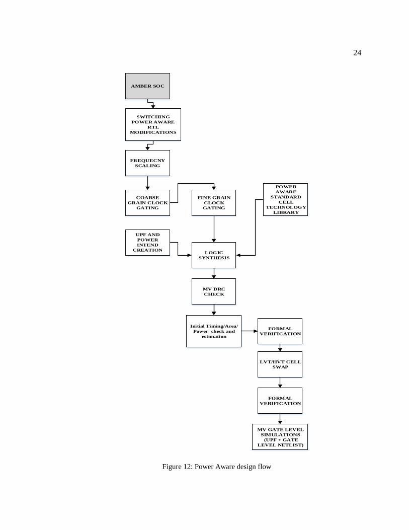
Figure 12 shows the approach followed in this project. In this flow, as verified AMBER SoC
HDL code that was already available was modified for the power aware RTL changes. Once
initial switching power aware RTL changes were completed, Synopsys formal verification tool
formality was used to run formal verification [15]. This verified that the functionality of the
design remained unchanged during the design flow. At this step, frequency-scaling module was
integrated with the design.
Next, clock gating is added. Clock gating cell types and location of fine grain clock gating cells
varies with different design requirements. More realistic and an efficient placement can be later
achieved during physical design flow.
After clock gating, we focused on multi VDD and multi Vt cells usage. UPF file was created to
divide the SoC system into different power domains and define power intent. UPF file syntax was
checked with mvcmp (Synopsys multi-voltage design suit) command. Synthesis tool (Design
Compiler) was used to synthesize the design along with UPF power optimization constraints.
More details about creating UPF power constraint file are discussed in section 3.2.5 of this
chapter.

23
After this multi voltage design rule check (DRC) static verification (MVRC) was performed; in
order to eliminate any risks from the design tape out schedule and ensures that structured low-
power design is functional.
At this point, depending upon physical design flow requirements, front-end design engineers can
consider critical timing path information and initial power estimation results and proceed with
replacing LVT cells with HVT cells for paths that are not timing critical well early in the design
cycle. Minimizing usage of LVT cells helps reducing leakage dissipation. In this project however,
different approach was taken and synthesis tool was given the choice to choose from mix of
HVT, LVT and SVT library cells to optimize design for leakage power dissipation. This
integrated approach of implementing multi VDD with multi Vt cells is supported by most of the
vendors and is highly recommended for quick results.
24
SWITCHING
POWER AWARE
RTL
MODIFICATIONS
AMBER SOC
FREQUECNY
SCALING
COARSE
GRAIN CLOCK
GATING
FINE GRAIN
CLOCK
GATING
UPF AND
POWER
INTEND
CREATION
POWER
AWARE
STANDARD
CELL
TECHNOLOGY
LIBRARY
LOGIC
SYNTHESIS
MV DRC
CHECK
Initial Timing/Area/
Power check and
estimation
FORMAL
VERIFICATION
LVT/HVT CELL
SWAP
FORMAL
VERIFICATION
MV GATE LEVEL
SIMULATIONS
(UPF + GATE
LEVEL NETLIST)
Figure 12: Power Aware design flow

25
3.2.2 Power aware RTL modifications
The source HDL code is originally written to work on Xilinx FPGA prototyping environment. As
there are limitations in terms of special function cells available on FPGA, the original source code
obtained from opensource.org was modified. With these changes, HDL code works in an ASIC
environment where standard cell library can be utilized to implement low power design
techniques.
The key changes to the existing RTL for Amber SoC were made to minimize the transitions on
the data. Most of the state encodings associated with the finite state machines (FSM) were either
binary or one-hot encoding. The FSMs were changed to gray encoding in order to minimize
transitions on state registers. We made changes to the Amber code, its cache blocks, Ethernet and
Wishbone module to minimize the data transitions. There were limited opportunities for
enhancements using resource sharing and free running counters. The examples of HDL
modifications for power aware RTL are shown in Appendix A.
3.2.2 Clock Gating
Power compiler was used to add clock gating to the design. During compilation of the
design -gate_clock option with compile_ultra command was used. Clock gating cell type
and constraints were selected based on the design analysis.
The set_clock_gating_style command was used to select clock gating cell types to be used in
AMBER SoC. This command takes the maximum fan-out of each clock-gating element and
minimum bit width of register banks that will be gated as the arguments. Bit width should be
carefully selected for the respective designs, as there will not be any power and area benefits due

26
to clock gating below certain minimum bit width. Based on initial experimental results obtained
from adding clock gating in Amber core, bit width of 20 was selected. There were different AND,
NAND, NOR, OR, latch and latch free clock gating styles supported by library vendor. There
were also enhanced clock gating styles available based on Exclusive OR logic. Integrated clock
gates are easy to use. Discrete clock gates were not preferred as latch based integrated clock gates
prevents glitches on the clock enable signals to the gated clock. These cells synchronizes the
clock gate control with clock to prevent glitches on clock signal. Hence, the power compiler was
allowed to pick integrated latch-based, clock gate (ICG) cells from the technology library.
Below are the steps implemented in the synthesis script:
1. Read the design related files (RTL preferably)
2. Set design environment.
3. Add timing, area and power optimization constraints
4. Set the power_driven_clock_gating to true
5. Set the clock-gating style
6. compile_ultra -gate_clock
7. Use the report_clock_gating command to report the registers and the clock gating cells
in the design.
8. Use the report_power command to get details of the power consumption
Design compiler script to add clock-gate cell used in AMBER SoC are shown in Appendix B.

27
3.2.3 Frequency Scaling
The frequency scaling was performed by adding a power down input port to the design. The
Ethernet IP strobe signal was used to override the power down signal to bring design into
powered up state. The power down mode design was made to run at half the specified frequency
except the Ethernet block that continues to run at specified frequency in order to wake the system
up from idle mode when required. Figure 13 shows divide-by-2 logic block followed by clock
mux controlled by signal freq_control_switch to scale down the clock frequencies by two. During
the synthesis, higher clock frequency is chosen at the clock mux outputs for timing checks. Note
that in reality adding multiplexers on the clock path is risky, and the special purpose balanced
clock mux cells should be selected to avoid any signal integrity and glitch related issues.
Figure 13: Frequency scaling block added to AMBER SoC
28
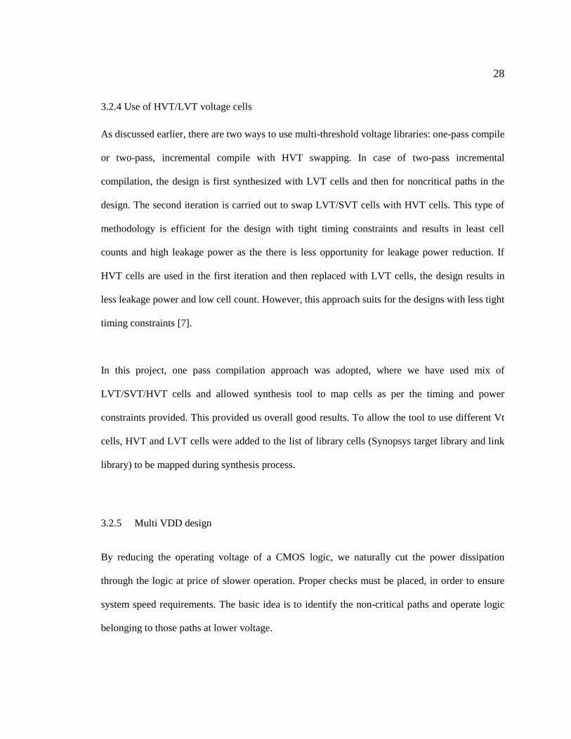
3.2.4 Use of HVT/LVT voltage cells
As discussed earlier, there are two ways to use multi-threshold voltage libraries: one-pass compile
or two-pass, incremental compile with HVT swapping. In case of two-pass incremental
compilation, the design is first synthesized with LVT cells and then for noncritical paths in the
design. The second iteration is carried out to swap LVT/SVT cells with HVT cells. This type of
methodology is efficient for the design with tight timing constraints and results in least cell
counts and high leakage power as the there is less opportunity for leakage power reduction. If
HVT cells are used in the first iteration and then replaced with LVT cells, the design results in
less leakage power and low cell count. However, this approach suits for the designs with less tight
timing constraints [7].
In this project, one pass compilation approach was adopted, where we have used mix of
LVT/SVT/HVT cells and allowed synthesis tool to map cells as per the timing and power
constraints provided. This provided us overall good results. To allow the tool to use different Vt
cells, HVT and LVT cells were added to the list of library cells (Synopsys target library and link
library) to be mapped during synthesis process.
3.2.5 Multi VDD design
By reducing the operating voltage of a CMOS logic, we naturally cut the power dissipation
through the logic at price of slower operation. Proper checks must be placed, in order to ensure
system speed requirements. The basic idea is to identify the non-critical paths and operate logic
belonging to those paths at lower voltage.

29
In this project, different but fixed supply voltages were applied to different blocks in the design.
Blocks operating at same supply voltage are said to belong to the same power domain. In this
design, three power domains were created, always on power domain (PD_AON), high voltage
on/off power domain (PD_HIGH) and on/off low voltage power domain (PD_LOW). Time
critical blocks were assigned to the high voltage and always-on power domains and less
noncritical blocks were assigned to low voltage power domains. Low voltage power domain
operates at 0.7V. High voltage and always-on power domain blocks were operated at 1.32V. This
multi VDD power intent was defined in IEEE 1801-2009 UPF format. Some of the common
important UPF commands used for the same are as follows [11]:
Design Navigation Commands: These commands are used to navigate across the design hierarchy
and apply power constraints to selected design hierarchy.
Example: set_scope, set _design_top
Supply Net Association Commands: These commands are used for creating and connecting
supply nets and ports as well as creating power switch.
Example: create_supply_port, create_supply_net, connect_supply_net, create_power_switch
Power Domain Commands: These commands are used for partitioning design based on different
power domains.
Example: create_power_domain, set_domain_supply_net, create_composite_domain
Power Intent Commands: These commands are used for defining power state and power intent.
Example: add_port_state, create_pst, add_pst_table, add_power_state, describe_state_transition
Attribute related Commands: These commands are used for setting up design, library or port
related attributes.
Example: set_port_attribute, set_design_attribute

30
Control logic Commands: These commands are used for creating control signals for power
management.
Example: create_logic_port, create_logic_net, connect_logic_net
Strategy related Commands: These commands are used for defining isolation, retention and level
shifter strategy for the UPF power intent.
Example: set_retention_elements, set_retention, set_retention_control,, set_isolation,
set_isolation_control, set_level_shifter
The power state table defined in the UPF file is shown in Table 2. Design is in state S2, when
whole design is powered up and all the three power domains are switched on. In state S0,
PD_LOW domain logic supply is switched off, whereas when the design is in state S3, PD_HIGH
domain is switched off. In state S1, both PD_HIGH and PD_LOW power domains switched off
and only PD_AON domain power supply is on. Synopsys® power compiler was used along with
the UPF file to create different power domains during the compilation and dynamic and leakage
power optimization during the power optimization phase of synthesis.
Table 2: Power state table
Power
state
VDD_HIGH VDD_LOW PD_LOW_SWITCH PD_HIGH_SWITCH
S0 HIGH LOW OFF ON
S1 HIGH LOW OFF OFF
S2 HIGH LOW ON ON
S3 HIGH LOW ON OFF

31
Figure 14 shows UPF diagram and power intent and provides brief idea about isolation and
retentions strategies as well as placement of level shifters used in this project.
Figure 15 shows different blocks of the Amber SoC and power domains.

32
Figure 14: Power domain/UPF diagram of AMBER SoC

33
AMBER CORE
UART1
DDR3 INTERFACE
TEST MODULE
BOOT MEMORY
TIMER
ETHERNET MAC
W
I
S
H
B
O
N
E
B
U
S
I
N
T
E
R
F
A
C
ECLOCK, CLOCK
MUX AND RESET
INTERRUPT
CONTROLLER
UART1
ALWAYS
ON
PD_LOW
(MORE
ON)
PD_HIGH
(LESS ON)
Figure 15: Block diagram of AMBER SoC as per power domain
The complete UPF file used in this design given in the Appendix B.

34
3.3 Power Estimation and Verification
Power aware design changes were verified using MVRC and formal equivalence (Synopsys
Formality) tools. Formal verification [15] was carried out every time design was subjected to
modifications.
3.3.1 Multi Voltage (MV) static verification
Static checking of the power intent was carried out using Synopsys MVRC tool. MVRC is multi
voltage rule checking tool, which checks whether the input UPF file and design files (RTL or
Gate level netlist) power connections are correct, and if special function cells correctly inserted at
the proper locations in the design. Synopsys® power compiler was allowed to run MVRC checks
using check_mv_design command, after the multi VDD synthesis process. In this project, the
MVRC rules were verified and few were waived off after analyzing the severity of the violations.
A sample set of MVRC violations reported during the synthesis are provided in Appendix B.
3.3.2 Power Estimation
For the initial power estimation, this project relied on Synopsys power compiler tool. The power
reports obtained for the AMBER SoC are provided in Appendix B. The report_power command
calculates and reports power for a design. The command uses user-annotated switching activity to
calculate the net switching power, cell internal power and cell leakage power, and displays the
calculated values in a power report. The report_power command reports internal, leakage and
switching power for the design. Power analysis uses the current tool's mechanism to obtain the
load capacitances. For example, wire load models are used for the case of non-back-annotated

35
(pre routed netlist) non-topographical mode synthesis; back-annotated capacitances are used
when these are available, and so forth. Wire load models (WLM) are used to estimate
interconnect delays based on pre layout static load values. WLM correlates impact of wire length
and fanout on resistance, capacitance and area of the nets. Topographical mode is where instead
of wire load models compiler uses actual post layout delay (resistance and capacitance) values,
which tightly correlates timing. The set_switching_activity command sets the switching activity
annotation on nets, pins, ports and cells of the current design. The report_power_calculation
command provides detailed power calculation information for the specified pin, cell, or net for
debugging or verifying power data in a technology library. The propagate_switching_activity
command forces the propagation of power-switching activity information. A user can specify the
effort level to be used during the propagation of the switching activity; however, default effort
level was used to gather power results. With higher effort level option, the tool uses the more
randomly generated switching activities to propagate the switching activity [4].

36
CHAPTER 4: RESULTS AND DISCUSSIONS
4.1 Results of low power implementations
In this project, power consumption and calculation results were obtained from Synopsys synthesis
tool, namely design compiler, which has built-in integrated power compiler. There were limited
opportunities for enhancements of original RTL using resource sharing and free running counters
to minimize data transitions, as a results original RTL was partially power aware. As a result,
original RTL power estimation do not give clear idea about impact of power aware RTL
modifications carried out in this project on power reduction. We have reported power estimation
of modified RTL. As discussed earlier, switching power is highly data variant and depends on the
data being present at a particular node. Here in this project, since the aim is to design and
implement low power design techniques from the front end design engineer’s perspective,
accurate results are not anticipated.
Table 3 shows the results obtained incrementally for the modified Amber SoC at three different
phases of the low power design flow. Power estimation results were obtained in three phases. In
first phase where power aware RTL changes were made including frequency scaling. In second
phase, power reports were obtained when clock gating was introduced in the design. Finally, in
the third phase multi Vt and multi VDD techniques were implemented, third phase results were
obtained using report_power command. Detailed power reports obtained during these three
phases are provided in Appendix B.

37
Table 3: AMBER SoC power results of modified RTL
Amber SoC
Dynamic
Power(uW)
Leakage
Power(pW)
Total
Power(uW)
After power aware RTL
modification 8.8425 247610000 256.4542
After adding Clock Gating 14.1323 82659000 96.7916
After adding Multi VDD + Multi Vt 2.9327 10544000 13.4763
Figure 16 shows column chart for the dynamic power dissipation. After adding multi VDD and
using multi Vt cells, dynamic power consumption seems to be reduced by 66%.
Figure 16: Modified Amber SoC -Dynamic power reduction results
𝐷𝑦𝑛𝑎𝑚𝑖𝑐 𝑝𝑜𝑤𝑒𝑟 𝑟𝑒𝑑𝑢𝑐𝑡𝑖𝑜𝑛 (%) =8.8425 − 2.9327
8.8425 = 66.83
0
2
4
6
8
10
12
14
16
power aware RTLmodifications
clock gating multi vdd+ multi vt
dynamic power (uW)

38
Figure 17: Modified Amber SoC Leakage power reduction
Figure 17 Shows column chart for the leakage power dissipation. After using HVT cells in Amber
SoC leakage power significantly reduced by 95%.
𝐿𝑒𝑎𝑘𝑎𝑔𝑒 𝑝𝑜𝑤𝑒𝑟 𝑟𝑒𝑑𝑢𝑐𝑡𝑖𝑜𝑛 (%) =247610000 − 10544000
247610000 = 95.74
0
50000000
100000000
150000000
200000000
250000000
300000000
power aware RTLmodifications
clock gating multi vdd+ multi vt
leakage power(pW)

39
Figure 18 shows column chart for total power consumption estimation obtained from initial
power report. With the use of clock gating and multi VDD techniques along with use of multi
threshold voltage cells proves reduction in power by 94%.
Figure 18: Modified Amber SoC Total power reduction
𝑇𝑜𝑡𝑎𝑙 𝑝𝑜𝑤𝑒𝑟 𝑟𝑒𝑑𝑢𝑐𝑡𝑖𝑜𝑛 (%) =256.4542 − 13.4763
256.4542 = 94.74
It should be noted that in sub threshold technologies (in this case 90 nm), leakage power
dissipation was observed to be a major factor in power dissipation. More accurate dynamic power
estimation can be performed using Switching Activity Interchange Format (SAIF) later when
actual capacitive load information is available post placement and routing [10].
0
50
100
150
200
250
300
power aware RTLmodifications
clock gating multi vdd+ multi vt
Total Power (uW)

40
CHAPTER 5: CONCLUSION
With decreasing feature sizes, hardware engineers have been able to pack billions of logic gates
on a given chip. A challenging problem to deal with is how to manage power in such high-
density chips, especially how to reduce the switching activity of the transistors and reduce the
leakage power dissipation. In addition, it is important to build balanced power management
systems, which scale with performance. Meeting the power consumption, speed, and area
constraints is one of the major challenges SoC designers face.
In this project, several power aware design techniques were applied to an existing SoC system.
We first revised the existing RTL code for the SOC system by introducing several power aware
coding constructs. Introduction of power aware HDL coding styles and RTL modifications
reduced the extent of data transitions in the design and led to reduction of the dynamic power
consumption very early in the design cycle. This process is simple and does not require any
additional efforts in terms of traditional front-end SoC design flow.
Next, we applied two clock-gating methods to this modified power aware SoC system. It was
observed that with the clock gating techniques, total power consumption can be significantly
reduced. We also found that performing design specific analysis of minimum bit-width
requirement is necessary for setting up fine grain clock gating topology and protocol. This helps
in meeting area and speed specifications of the design easily during the physical design cycle.
Results of our experiments illustrated that applying reduced supply voltage to the less time
critical design blocks and dividing the SoC system into different power domains furthermore
reduced impact of supply voltage on dynamic, short circuit and leakage power dissipation. We
41
found that addition of power gating to be another important technique in scaling down impact of
VDD on power domain logic that is in standby or idle mode.
We explored the use of multiple threshold voltage cells in order to minimize the effect of power
gating and reduced supply voltage on leakage power dissipation. We observed that use of multi-
threshold voltage cells is an effective technique to reduce the leakage power. Adding more, multi
Vt and multi VDD power reduction techniques can also be integrated in one flow to avoid
iterative design cycles. However, this approach still needs to be verified from the physical design
engineer's perspective.
Clock gating and multi Vt techniques are relatively simple to implement and require less design
and verification efforts in front end design cycle. However, applying multiple supply voltages to
the design blocks to reduce the impact of VDD requires special design considerations and
additional efforts to implement. Standard cell library should provide different special function
cells in order to implement power intent defined in UPF file.
We presented initial power estimation results obtained from the synthesis tool. We showed that
the modified SoC system would be able to reduce total power consumption by a considerable
amount. With clock-gating and power aware RTL changes, total power was reduced by 60
percentages. With additional efforts on implementing multi-VDD and multi-Vt techniques, we
were able to achieve reduction in total power by 90 percentages. A more detailed and accurate
power analysis can be done on the entire system to find out data variant dynamic power
consumption and impact of accurate capacitive load information at different phases of the design
cycles. However, we leave this as a part of future work.

42
Appendix A: Power aware RTL modifications
Following section shows power aware modifications done to the original HDL
////////////////////////////////////////////////////////////////////////////////////////////////////////////////////
// Copyright (C) 2011 Authors and OPENCORES.ORG //
// This source file may be used and distributed without //
// restriction provided that this copyright statement is not //
// removed from the file and that any derivative work contains //
// the original copyright notice and the associated disclaimer. //
// This source file is free software; you can redistribute it //
// and/or modify it under the terms of the GNU Lesser General //
// Public License as published by the Free Software Foundation; //
// either version 2.1 of the License, or (at your option) any //
// later version. //
// This source is distributed in the hope that it will be //
// useful, but WITHOUT ANY WARRANTY; without even the implied //
// warranty of MERCHANTABILITY or FITNESS FOR A PARTICULAR //
// PURPOSE. See the GNU Lesser General Public License for more //
// details. //
// You should have received a copy of the GNU Lesser General //
// Public License along with this source; if not, download it //
// from http://www.opencores.org/lgpl.shtml //
//////////////////////////////////////////////////////////////////////////////////////////////////////////////////
Original HDL Power aware RTL modifications
// FILE NAME: a25_icache.v localparam [3:0] CS_INIT = 4'd0, CS_IDLE = 4'd1, CS_FILL0 = 4'd2, CS_FILL1 = 4'd3, CS_FILL2 = 4'd4, CS_FILL3 = 4'd5,
// FILE NAME: a25_icache.v // changed to gray encoding localparam [3:0] CS_INIT = 4'b0000, CS_IDLE = 4'b0001, CS_FILL0 = 4'b0011, CS_FILL1 = 4'b0010, CS_FILL2 = 4'b0110,

43
CS_FILL4 = 4'd6, CS_FILL_COMPLETE = 4'd7, CS_TURN_AROUND = 4'd8, CS_WRITE_HIT1 = 4'd9, CS_EX_DELETE = 4'd10;
CS_FILL3 = 4'b0111, CS_FILL4 = 4'b0101, CS_FILL_COMPLETE = 4'b0100, CS_TURN_AROUND = 4'b1100, CS_WRITE_HIT1 = 4'b1101, CS_EX_DELETE = 4'b1111;
// FILE NAME: a25_icache.v always@(posedge i_clk)
// FILE NAME: a25_icache.v // Added For Clock gating // ====================================== // Read Buffer // ====================================== always@(posedge i_clk) begin if(i_cg_en)
// all always@(posedge i_clk) procedural blocks were
modified in such a way
//FILE NAME: a25_core.v //FILE NAME: a25_core.v // Added For Clock gating input i_cg_en_fetch, // added clock gating input i_cg_en_decode, // added clock gating input i_cg_en_execute, // added clock gating input i_cg_en_mem, // added clock gating input i_cg_en_write_back, // added clock gating input i_cg_en_wishbone, // added clock gating input i_cg_en_coprocessor // added_clock_gatin
// FILE NAME: a25_multiply.v always @ ( posedge i_clk ) if ( !i_core_stall ) begin count <= i_execute ? count_nxt :
count; product <= i_execute ?
product_nxt : product; o_done <= i_execute ? count
== 6'd31 : o_done; end
// FILE NAME: a25_multiply.v // Added For Clock gating always @ ( posedge i_clk ) begin if(i_cg_en) begin if ( !i_core_stall ) begin count <= i_execute ? count_nxt : count;
product <= i_execute ? product_nxt
: product; o_done <= i_execute ? count ==
6'd31 : o_done; end end end
//FILE NAME: a25_barel_shift.v always @(posedge i_clk) begin full_out_r <= full_out; full_carry_out_r <= full_carry_out;
//FILE NAME: a25_barel_shift.v // Added For Clock gating always @(posedge i_clk) begin if(i_cg_en)

44
use_quick_r <= !o_stall; end
begin begin full_out_r <= full_out; full_carry_out_r <= full_carry_out; use_quick_r <= !o_stall; end end end
//FILE NAME: a25_shifter.v always@( posedge i_clk ) if ( i_wb_read_data_valid ) begin read_data_filtered_r <= read_data_filtered; load_rd_r <= i_wb_load_rd[3:0]; end
//FILE NAME: a25_shifter.v // Added For Clock gating always@( posedge i_clk ) begin if(i_cg_en) begin if ( i_wb_read_data_valid ) begin read_data_filtered_r <= read_data_filtered; load_rd_r <= i_wb_load_rd[3:0]; end end end
// FILENAME : a25_wishbone.v always @(posedge i_clk) begin if (new_access) begin if (wbuf_valid[0]) begin o_wb_adr <= wbuf_addr [0]; o_wb_sel <= wbuf_be [0]; o_wb_we <= wbuf_write[0]; o_wb_dat <= wbuf_wdata[0]; o_wb_cyc <= 1'd1; o_wb_stb <= 1'd1; serving_port <= 3'b001; end else if (wbuf_valid[1]) begin o_wb_adr <= wbuf_addr [1]; o_wb_sel <= wbuf_be [1]; o_wb_we <= wbuf_write[1]; o_wb_dat <= wbuf_wdata[1]; o_wb_cyc <= 1'd1; o_wb_stb <= 1'd1; serving_port <= 3'b010; end else if (wbuf_valid[2]) begin o_wb_adr <= wbuf_addr [2]; o_wb_sel <= wbuf_be [2];
// FILENAME : a25_wishbone.v always @(posedge i_clk) begin // Added For Clock gating if(i_cg_en) begin begin if (new_access) begin if (wbuf_valid[0]) begin o_wb_adr <= wbuf_addr [0]; o_wb_sel <= wbuf_be [0]; o_wb_we <= wbuf_write[0]; o_wb_dat <= wbuf_wdata[0]; o_wb_cyc <= 1'd1; o_wb_stb <= 1'd1; serving_port <= 3'b001; end else if (wbuf_valid[1]) begin o_wb_adr <= wbuf_addr [1]; o_wb_sel <= wbuf_be [1]; o_wb_we <= wbuf_write[1]; o_wb_dat <= wbuf_wdata[1]; o_wb_cyc <= 1'd1; o_wb_stb <= 1'd1; serving_port <= 3'b010; end

45
o_wb_we <= wbuf_write[2]; o_wb_dat <= wbuf_wdata[2]; o_wb_cyc <= 1'd1; o_wb_stb <= 1'd1; serving_port <= 3'b100; end else begin o_wb_cyc <= 1'd0; o_wb_stb <= 1'd0; // Don't need to change these values
because they are ignored // when stb is low, but it makes for a
cleaner waveform, at the expense of a few gates o_wb_we <= 1'd0; o_wb_adr <= 'd0; o_wb_dat <= 'd0; serving_port <= 3'b000; end end end
else if (wbuf_valid[2]) begin o_wb_adr <= wbuf_addr [2]; o_wb_sel <= wbuf_be [2]; o_wb_we <= wbuf_write[2]; o_wb_dat <= wbuf_wdata[2]; o_wb_cyc <= 1'd1; o_wb_stb <= 1'd1; serving_port <= 3'b100; end else begin o_wb_cyc <= 1'd0; o_wb_stb <= 1'd0; // MODIFIED FOR POWER AWARE RTL // Don't need to change these values because they
are ignored // when stb is low, but it makes for a cleaner
waveform, at the expense of a few gates // COMMENTED o_wb_we <= 1'd0; // COMMENTED o_wb_adr <= 'd0; // COMMENTED o_wb_dat <= 'd0; // COMMENTED // COMMENTED serving_port <=
3'b000; end end end end end
//FILE NAME: a25_mem.V always @( posedge i_clk ) begin uncached_wb_req_r <=
(o_wb_uncached_req || uncached_wb_req_r) &&
!i_wb_uncached_ready; end
//FILE NAME: a25_mem.V always @( posedge i_clk ) begin // Added For Clock gating if(i_cg_en) begin begin uncached_wb_req_r <= (o_wb_uncached_req ||
uncached_wb_req_r) && !i_wb_uncached_ready; end end end
// all always@(posedge i_clk) procedural blocks were
modified in such a way
//FILE NAME : a25_dcache.V localparam [3:0] CS_INIT = 4'd0, CS_IDLE = 4'd1, CS_FILL = 4'd2,
//FILE NAME : a25_dcache.V // changed to gray encoding localparam [3:0] CS_INIT = 4'b0000, CS_IDLE = 4'b0001,

46
CS_FILL_COMPLETE = 4'd3, CS_TURN_AROUND = 4'd4, CS_WRITE_HIT = 4'd5, CS_WRITE_HIT_WAIT_WB = 4'd6, CS_WRITE_MISS_WAIT_WB = 4'd7, CS_EX_DELETE = 4'd8;
CS_FILL = 4'b0011, CS_FILL_COMPLETE = 4'b0010, CS_TURN_AROUND = 4'b0110, CS_WRITE_HIT = 4'b0111, CS_WRITE_HIT_WAIT_WB = 4'b0101, CS_WRITE_MISS_WAIT_WB = 4'b0100, CS_EX_DELETE = 4'b1100; // all always@(posedge i_clk) procedural blocks were
modified in such a way
// FILE NAME: a25_register.v //=====================================
================== // Register Update //
======================================
================== always @ ( posedge i_clk ) begin // these registers are used in all modes r0 <= reg_bank_wen_c[0 ]
? i_reg : read_data_wen[0 ] ?
i_wb_read_data : r0; r1 <= reg_bank_wen_c[1 ]
? i_reg : read_data_wen[1 ] ?
i_wb_read_data : r1; r2 <= reg_bank_wen_c[2 ]
? i_reg : read_data_wen[2 ] ?
i_wb_read_data : r2; r3 <= reg_bank_wen_c[3 ]
? i_reg : read_data_wen[3 ] ?
i_wb_read_data : r3; r4 <= reg_bank_wen_c[4 ]
? i_reg : read_data_wen[4 ] ?
i_wb_read_data : r4; r5 <= reg_bank_wen_c[5 ]
? i_reg : read_data_wen[5 ] ?
i_wb_read_data : r5; r6 <= reg_bank_wen_c[6 ]
? i_reg : read_data_wen[6 ] ?
i_wb_read_data : r6; r7 <= reg_bank_wen_c[7 ]
? i_reg : read_data_wen[7 ] ?
i_wb_read_data : r7; // these registers are used in all modes,
except fast irq r8 <= reg_bank_wen_c[8 ] &&
!firq_idec ? i_reg : read_data_wen[8 ] &&
i_wb_mode != FIRQ ? i_wb_read_data :
r8; r9 <= reg_bank_wen_c[9 ] &&
!firq_idec ? i_reg : read_data_wen[9 ] &&
i_wb_mode != FIRQ ? i_wb_read_data :
// FILE NAME: a25_register.v //
==========================================
============== // Register Update //
==========================================
============== always @ ( posedge i_clk ) begin // Added For Clock gating if(i_cg_en) begin begin // these registers are used in all modes r0 <= reg_bank_wen_c[0 ]
? i_reg : read_data_wen[0 ] ?
i_wb_read_data : r0; r1 <= reg_bank_wen_c[1 ]
? i_reg : read_data_wen[1 ] ?
i_wb_read_data : r1; r2 <= reg_bank_wen_c[2 ]
? i_reg : read_data_wen[2 ] ?
i_wb_read_data : r2; r3 <= reg_bank_wen_c[3 ]
? i_reg : read_data_wen[3 ] ?
i_wb_read_data : r3; r4 <= reg_bank_wen_c[4 ]
? i_reg : read_data_wen[4 ] ?
i_wb_read_data : r4; r5 <= reg_bank_wen_c[5 ]
? i_reg : read_data_wen[5 ] ?
i_wb_read_data : r5; r6 <= reg_bank_wen_c[6 ]
? i_reg : read_data_wen[6 ] ?
i_wb_read_data : r6; r7 <= reg_bank_wen_c[7 ]
? i_reg : read_data_wen[7 ] ?
i_wb_read_data : r7; // these registers are used in all modes, except
fast irq r8 <= reg_bank_wen_c[8 ] && !firq_idec
? i_reg : read_data_wen[8 ] && i_wb_mode != FIRQ ?

47
r9; r10 <= reg_bank_wen_c[10] &&
!firq_idec ? i_reg : read_data_wen[10] &&
i_wb_mode != FIRQ ? i_wb_read_data :
r10; r11 <= reg_bank_wen_c[11] &&
!firq_idec ? i_reg : read_data_wen[11] &&
i_wb_mode != FIRQ ? i_wb_read_data :
r11; r12 <= reg_bank_wen_c[12] &&
!firq_idec ? i_reg : read_data_wen[12] &&
i_wb_mode != FIRQ ? i_wb_read_data :
r12; // these registers are used in fast irq mode r8_firq <= reg_bank_wen_c[8 ] &&
firq_idec ? i_reg : read_data_wen[8 ] &&
i_wb_mode == FIRQ ? i_wb_read_data :
r8_firq; r9_firq <= reg_bank_wen_c[9 ] &&
firq_idec ? i_reg : read_data_wen[9 ] &&
i_wb_mode == FIRQ ? i_wb_read_data :
r9_firq; r10_firq <= reg_bank_wen_c[10] &&
firq_idec ? i_reg : read_data_wen[10] &&
i_wb_mode == FIRQ ? i_wb_read_data :
r10_firq; r11_firq <= reg_bank_wen_c[11] &&
firq_idec ? i_reg : read_data_wen[11] &&
i_wb_mode == FIRQ ? i_wb_read_data :
r11_firq; r12_firq <= reg_bank_wen_c[12] &&
firq_idec ? i_reg : read_data_wen[12] &&
i_wb_mode == FIRQ ? i_wb_read_data :
r12_firq; // these registers are used in user mode r13 <= reg_bank_wen_c[13] &&
usr_idec ? i_reg : read_data_wen[13] &&
i_wb_mode == USR ? i_wb_read_data :
r13; r14 <= reg_bank_wen_c[14] &&
usr_idec ? i_reg : read_data_wen[14] &&
i_wb_mode == USR ? i_wb_read_data :
r14; // these registers are used in supervisor
mode r13_svc <= reg_bank_wen_c[13] &&
svc_idec ? i_reg : read_data_wen[13] &&
i_wb_mode == SVC ? i_wb_read_data :
r13_svc; r14_svc <= reg_bank_wen_c[14] &&
svc_idec ? i_reg : read_data_wen[14] &&
i_wb_mode == SVC ? i_wb_read_data :
r14_svc;
i_wb_read_data : r8; r9 <= reg_bank_wen_c[9 ] && !firq_idec
? i_reg : read_data_wen[9 ] && i_wb_mode != FIRQ ?
i_wb_read_data : r9; r10 <= reg_bank_wen_c[10] && !firq_idec
? i_reg : read_data_wen[10] && i_wb_mode != FIRQ ?
i_wb_read_data : r10; r11 <= reg_bank_wen_c[11] && !firq_idec
? i_reg : read_data_wen[11] && i_wb_mode != FIRQ ?
i_wb_read_data : r11; r12 <= reg_bank_wen_c[12] && !firq_idec
? i_reg : read_data_wen[12] && i_wb_mode != FIRQ ?
i_wb_read_data : r12; // these registers are used in fast irq mode r8_firq <= reg_bank_wen_c[8 ] && firq_idec ?
i_reg : read_data_wen[8 ] && i_wb_mode == FIRQ ?
i_wb_read_data : r8_firq; r9_firq <= reg_bank_wen_c[9 ] && firq_idec ?
i_reg : read_data_wen[9 ] && i_wb_mode == FIRQ ?
i_wb_read_data : r9_firq; r10_firq <= reg_bank_wen_c[10] && firq_idec
? i_reg : read_data_wen[10] && i_wb_mode == FIRQ ?
i_wb_read_data : r10_firq; r11_firq <= reg_bank_wen_c[11] && firq_idec
? i_reg : read_data_wen[11] && i_wb_mode == FIRQ ?
i_wb_read_data : r11_firq; r12_firq <= reg_bank_wen_c[12] && firq_idec
? i_reg : read_data_wen[12] && i_wb_mode == FIRQ ?
i_wb_read_data : r12_firq; // these registers are used in user mode r13 <= reg_bank_wen_c[13] && usr_idec
? i_reg : read_data_wen[13] && i_wb_mode == USR ?
i_wb_read_data : r13; r14 <= reg_bank_wen_c[14] && usr_idec
? i_reg : read_data_wen[14] && i_wb_mode == USR ?
i_wb_read_data : r14; // these registers are used in supervisor mode r13_svc <= reg_bank_wen_c[13] && svc_idec
? i_reg : read_data_wen[13] && i_wb_mode == SVC ?
i_wb_read_data : r13_svc; r14_svc <= reg_bank_wen_c[14] && svc_idec
? i_reg : read_data_wen[14] && i_wb_mode == SVC ?
i_wb_read_data : r14_svc; // these registers are used in irq mode r13_irq <= reg_bank_wen_c[13] && irq_idec ?
i_reg : read_data_wen[13] && i_wb_mode == IRQ ?
i_wb_read_data : r13_irq; r14_irq <= (reg_bank_wen_c[14] && irq_idec)
? i_reg : read_data_wen[14] && i_wb_mode == IRQ ?
i_wb_read_data : r14_irq; // these registers are used in fast irq mode

48
// these registers are used in irq mode r13_irq <= reg_bank_wen_c[13] &&
irq_idec ? i_reg : read_data_wen[13] &&
i_wb_mode == IRQ ? i_wb_read_data :
r13_irq; r14_irq <= (reg_bank_wen_c[14] &&
irq_idec) ? i_reg : read_data_wen[14] &&
i_wb_mode == IRQ ? i_wb_read_data :
r14_irq; // these registers are used in fast irq mode r13_firq <= reg_bank_wen_c[13] &&
firq_idec ? i_reg : read_data_wen[13] &&
i_wb_mode == FIRQ ? i_wb_read_data :
r13_firq; r14_firq <= reg_bank_wen_c[14] &&
firq_idec ? i_reg : read_data_wen[14] &&
i_wb_mode == FIRQ ? i_wb_read_data :
r14_firq; // these registers are used in all modes r15 <= pc_wen_c ?
i_pc : pc_dmem_wen ?
i_wb_read_data[25:2] : r15; end
r13_firq <= reg_bank_wen_c[13] && firq_idec
? i_reg : read_data_wen[13] && i_wb_mode == FIRQ ?
i_wb_read_data : r13_firq; r14_firq <= reg_bank_wen_c[14] && firq_idec
? i_reg : read_data_wen[14] && i_wb_mode == FIRQ ?
i_wb_read_data : r14_firq; // these registers are used in all modes r15 <= pc_wen_c ? i_pc :
pc_dmem_wen ?
i_wb_read_data[25:2] : r15; end end end
// all always@(posedge i_clk) procedural blocks were
modified in such a way
//FILE NAME : eth_receivecontrol.v // Byte counter always @ (posedge MRxClk or posedge RxReset) begin if(RxReset) ByteCnt[4:0] <= 5'h0; else if(ResetByteCnt) ByteCnt[4:0] <= 5'h0; else if(IncrementByteCnt) ByteCnt[4:0] <= ByteCnt[4:0] + 1'b1; end
// EXAMPLE OF CONTROLLING COUNTER
49
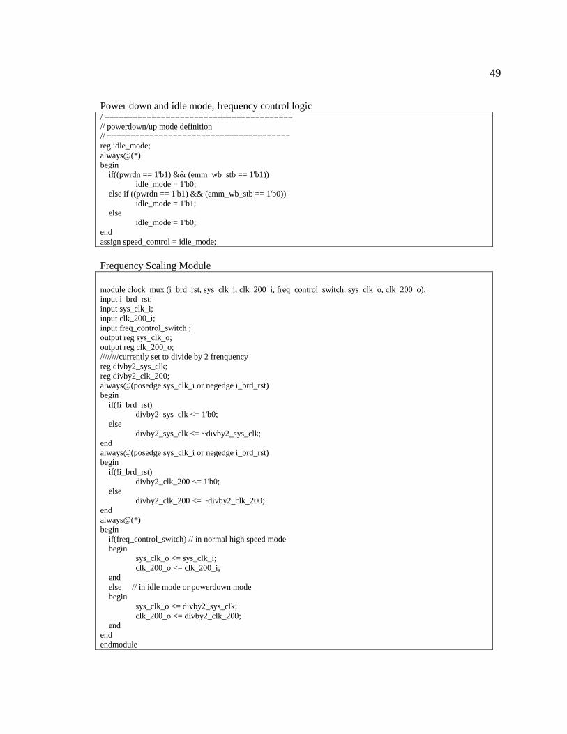
Power down and idle mode, frequency control logic / ======================================== // powerdown/up mode definition // ======================================= reg idle_mode; always@(*) begin if((pwrdn == 1'b1) && (emm_wb_stb == 1'b1)) idle_mode = 1'b0; else if ((pwrdn == 1'b1) && (emm_wb_stb == 1'b0)) idle_mode = 1'b1; else idle_mode = 1'b0; end assign speed_control = idle_mode; Frequency Scaling Module
module clock_mux (i_brd_rst, sys_clk_i, clk_200_i, freq_control_switch, sys_clk_o, clk_200_o); input i_brd_rst; input sys_clk_i; input clk_200_i; input freq_control_switch ; output reg sys_clk_o; output reg clk_200_o; ////////currently set to divide by 2 frenquency reg divby2_sys_clk; reg divby2_clk_200; always@(posedge sys_clk_i or negedge i_brd_rst) begin if(!i_brd_rst) divby2_sys_clk <= 1'b0; else divby2_sys_clk <= ~divby2_sys_clk; end always@(posedge sys_clk_i or negedge i_brd_rst) begin if(!i_brd_rst) divby2_clk_200 <= 1'b0; else divby2_clk_200 <= ~divby2_clk_200; end always@(*) begin if(freq_control_switch) // in normal high speed mode begin sys_clk_o <= sys_clk_i; clk_200_o <= clk_200_i; end else // in idle mode or powerdown mode begin sys_clk_o <= divby2_sys_clk; clk_200_o <= divby2_clk_200; end end endmodule

50
Appendix B: Design Implementation scripts, Reports, Violations
Clock gating synthesis script
#Read the design in
read_file -format verilog {"rtl_list.v"}
set current_design system
#Link the design
link
#create clock and constrain the design
create_clock "brd_clk_p" -period 5 -name "brd_clk_p" -waveform [list 0 2.5]
create_clock "brd_clk_n" -period 5 -name "brd_clk_n" -waveform [list 2.5 5]
create_generated_clock -name "sys_clk" -divide_by 2 -source "brd_clk_p" [get_pins u_var_freq_switch/sys_clk_o]
create_generated_clock -name "clk_200" -divide_by 4 -source "brd_clk_p" [get_pins u_var_freq_switch/clk_200_o]
set_input_delay -clock brd_clk_p -max -rise 1 [all_inputs]
set_input_delay -clock brd_clk_p -min -rise 0.9 [all_inputs]
set_input_delay -clock brd_clk_p -max -fall 1 [all_inputs]
set_input_delay -clock brd_clk_p -min -fall 0.9 [all_inputs]
set_output_delay -clock brd_clk_p -max -rise 1.1 [all_outputs]
set_output_delay -clock brd_clk_p -min -rise 0.8 [all_outputs]
set_output_delay -clock brd_clk_p -max -fall 1.1 [all_outputs]
set_output_delay -clock brd_clk_p -min -fall 0.8 [all_outputs]
set_input_delay -clock brd_clk_n -max -rise 1 [all_inputs]
set_input_delay -clock brd_clk_n -min -rise 0.9 [all_inputs]
set_input_delay -clock brd_clk_n -max -fall 1 [all_inputs]
set_input_delay -clock brd_clk_n -min -fall 0.9 [all_inputs]
set_output_delay -clock brd_clk_n -max -rise 1.1 [all_outputs]
set_output_delay -clock brd_clk_n -min -rise 0.8 [all_outputs]
set_output_delay -clock brd_clk_n -max -fall 1.1 [all_outputs]
set_output_delay -clock brd_clk_n -min -fall 0.8 [all_outputs]

51
set_input_delay -clock sys_clk -max -rise 1 [all_inputs]
set_input_delay -clock sys_clk -min -rise 0.9 [all_inputs]
set_input_delay -clock sys_clk -max -fall 1 [all_inputs]
set_input_delay -clock sys_clk -min -fall 0.9 [all_inputs]
set_output_delay -clock sys_clk -max -rise 1.1 [all_outputs]
set_output_delay -clock sys_clk -min -rise 0.8 [all_outputs]
set_output_delay -clock sys_clk -max -fall 1.1 [all_outputs]
set_output_delay -clock sys_clk -min -fall 0.8 [all_outputs]
set_input_delay -clock clk_200 -max -rise 1 [all_inputs]
set_input_delay -clock clk_200 -min -rise 0.9 [all_inputs]
set_input_delay -clock clk_200 -max -fall 1 [all_inputs]
set_input_delay -clock clk_200 -min -fall 0.9 [all_inputs]
set_output_delay -clock clk_200 -max -rise 1.1 [all_outputs]
set_output_delay -clock clk_200 -min -rise 0.8 [all_outputs]
set_output_delay -clock clk_200 -max -fall 1.1 [all_outputs]
set_output_delay -clock clk_200 -min -fall 0.8 [all_outputs]
set_dont_touch_network {clk_200 sys_clk brd_rst brd_clk_p brd_clk_n brd_rst}
set_false_path -from {clk_200} -to {sys_clk brd_clk_p brd_clk_n}
set_false_path -from {sys_clk} -to {clk_200 brd_clk_p brd_clk_n}
set_false_path -from {brd_clk_p} -to {sys_clk clk_200 brd_clk_n}
set_false_path -from {brd_clk_n} -to {sys_clk clk_200 brd_clk_p}
set_clock_groups -async -group sys_clk -group clk_200 -group brd_clk_p -group brd_clk_n
set_max_area 0
#Set operating conditions
set_operating_conditions -library "saed90nm_typ" "TYPICAL"
set_operating_conditions -library "saed90nm_typ_cg" "TYPICAL"
uniquify
set_clock_gating_style -sequential_cell latch \
-positive_edge_logic integrated \

52
-negative_edge_logic integrated \
-control_point before \
-max_fanout 20 \
-minimum_bitwidth 20
insert_clock_gating
compile_ultra -gate_clock
report_clock_gating
AMBER UPF file
### Create Power Domains
create_power_domain TOP
create_power_domain PD_AON -elements {u_amber u_eth_top u_ethmac_wb}
create_power_domain PD_LOW -elements {u_timer_module u_boot_mem u_wishbone_arbiter
u_wb_xs6_ddr3_bridge}
create_power_domain PD_HIGH -elements {u_uart0 u_uart1 u_interrupt_controller}
### Top level Connections
### for VDD_HIGH (1.32V)
create_supply_port VDD_HIGH
create_supply_net VDD_HIGH -domain TOP
create_supply_net VDD_HIGH -domain PD_AON -reuse
create_supply_net VDD_HIGH -domain PD_HIGH -reuse
connect_supply_net VDD_HIGH -ports VDD_HIGH
### for VDD_LOW (0.7V)
create_supply_port VDD_LOW
create_supply_net VDD_LOW -domain TOP

53
create_supply_net VDD_LOW -domain PD_LOW -reuse
connect_supply_net VDD_LOW -ports VDD_LOW
### for VSS (0.0V)
create_supply_port VSS
create_supply_net VSS -domain TOP
create_supply_net VSS -domain PD_AON -reuse
create_supply_net VSS -domain PD_LOW -reuse
create_supply_net VSS -domain PD_HIGH -reuse
connect_supply_net VSS -ports VSS
### PD_LOW/CRC DOMAIN Power Connections
create_supply_net VDD_LOW_VIRTUAL -domain PD_LOW
create_supply_net VDD_HIGH_VIRTUAL -domain PD_HIGH
### Associate Supply Nets at the top level
set_domain_supply_net TOP -primary_power_net VDD_HIGH -primary_ground_net VSS
set_domain_supply_net PD_AON -primary_power_net VDD_HIGH -primary_ground_net VSS
set_domain_supply_net PD_LOW -primary_power_net VDD_LOW_VIRTUAL -primary_ground_net VSS
set_domain_supply_net PD_HIGH -primary_power_net VDD_HIGH_VIRTUAL -primary_ground_net VSS
###Power Switch to Shut-Down a Block
create_power_switch pdlow_sw -domain PD_LOW -input_supply_port {ps_in VDD_LOW} -output_supply_port
{ps_out VDD_LOW_VIRTUAL} -control_port {pdlow_sd system_rdy} -on_state {ON_STATE_PD_LOW ps_in
{!pdlow_sd}}
create_power_switch pdhigh_sw -domain PD_HIGH -input_supply_port {ps_in VDD_HIGH} -output_supply_port
{ps_out VDD_HIGH_VIRTUAL} -control_port {pdhigh_sd uart0_int} -on_state {ON_STATE_PD_HIGH ps_in
{!pdhigh_sd}}

54
### Isolation Strategy
set_isolation pd_low_iso_out -domain PD_LOW -isolation_power_net VDD_HIGH -isolation_ground_net VSS -
clamp_value 1 -applies_to outputs
set_isolation_control pd_low_iso_out -domain PD_LOW -isolation_signal uart0_int -isolation_sense low -location
parent
### Retention Strategy
set_retention pdhigh_retain -domain PD_HIGH -retention_power_net VDD_HIGH -retention_ground_net VSS
set_retention_control pdhigh_retain -domain PD_HIGH -save_signal {u_interrupt_controller/o_firq high} -
restore_signal {u_uart0/o_uart_int high}
### Level Shifter Strategy
set_level_shifter PD_AON_ls_out -domain PD_AON -applies_to outputs -location self -rule both
### Power State Table
add_port_state VDD_HIGH -state {HighVoltage 1.32}
add_port_state VDD_LOW -state {LowVoltage 0.7}
add_port_state pdhigh_sw/ps_out -state {HighVoltage 1.32} -state {PD_HIGH_OFF off}
add_port_state pdlow_sw/ps_out -state {LowVoltage 0.7} -state {PD_LOW_OFF off}
create_pst lvds_system_pst -supplies {VDD_HIGH VDD_LOW VDD_HIGH_VIRTUAL
VDD_LOW_VIRTUAL}
add_pst_state PRE_BOOT -pst lvds_system_pst -state { HighVoltage LowVoltage PD_HIGH_OFF
PD_LOW_OFF}
add_pst_state PD_HIGH_ON -pst lvds_system_pst -state { HighVoltage LowVoltage HighVoltage PD_LOW_OFF}
add_pst_state PD_LOW_ON -pst lvds_system_pst -state { HighVoltage LowVoltage PD_HIGH_OFF LowVoltage}
add_pst_state ALL_ON -pst lvds_system_pst -state { HighVoltage LowVoltage HighVoltage LowVoltage}

55
Multi VDD + Clock Gating + Mixed Vt cells: synthesis script
#Read the design in
read_file -format verilog
{"/gaia/home/project/prj_lp14/msproject/expt/amber/trunk/hw/vlog/power_aware_rtl_changes/amber25/rtl_list.v"}
set current_design system
#Link the design
link
#create clock and constrain the design
create_clock "brd_clk_p" -period 5 -name "brd_clk_p" -waveform [list 0 2.5]
create_clock "brd_clk_n" -period 5 -name "brd_clk_n" -waveform [list 2.5 5]
create_generated_clock -name "sys_clk" -divide_by 2 -source "brd_clk_p" [get_pins u_var_freq_switch/sys_clk_o]
create_generated_clock -name "clk_200" -divide_by 4 -source "brd_clk_p" [get_pins u_var_freq_switch/clk_200_o]
set_input_delay -clock brd_clk_p -max -rise 1 [all_inputs]
set_input_delay -clock brd_clk_p -min -rise 0.9 [all_inputs]
set_input_delay -clock brd_clk_p -max -fall 1 [all_inputs]
set_input_delay -clock brd_clk_p -min -fall 0.9 [all_inputs]
set_output_delay -clock brd_clk_p -max -rise 1.1 [all_outputs]
set_output_delay -clock brd_clk_p -min -rise 0.8 [all_outputs]
set_output_delay -clock brd_clk_p -max -fall 1.1 [all_outputs]
set_output_delay -clock brd_clk_p -min -fall 0.8 [all_outputs]
set_input_delay -clock brd_clk_n -max -rise 1 [all_inputs]
set_input_delay -clock brd_clk_n -min -rise 0.9 [all_inputs]
set_input_delay -clock brd_clk_n -max -fall 1 [all_inputs]
set_input_delay -clock brd_clk_n -min -fall 0.9 [all_inputs]
set_output_delay -clock brd_clk_n -max -rise 1.1 [all_outputs]
set_output_delay -clock brd_clk_n -min -rise 0.8 [all_outputs]
set_output_delay -clock brd_clk_n -max -fall 1.1 [all_outputs]

56
set_output_delay -clock brd_clk_n -min -fall 0.8 [all_outputs]
set_input_delay -clock sys_clk -max -rise 1 [all_inputs]
set_input_delay -clock sys_clk -min -rise 0.9 [all_inputs]
set_input_delay -clock sys_clk -max -fall 1 [all_inputs]
set_input_delay -clock sys_clk -min -fall 0.9 [all_inputs]
set_output_delay -clock sys_clk -max -rise 1.1 [all_outputs]
set_output_delay -clock sys_clk -min -rise 0.8 [all_outputs]
set_output_delay -clock sys_clk -max -fall 1.1 [all_outputs]
set_output_delay -clock sys_clk -min -fall 0.8 [all_outputs]
set_input_delay -clock clk_200 -max -rise 1 [all_inputs]
set_input_delay -clock clk_200 -min -rise 0.9 [all_inputs]
set_input_delay -clock clk_200 -max -fall 1 [all_inputs]
set_input_delay -clock clk_200 -min -fall 0.9 [all_inputs]
set_output_delay -clock clk_200 -max -rise 1.1 [all_outputs]
set_output_delay -clock clk_200 -min -rise 0.8 [all_outputs]
set_output_delay -clock clk_200 -max -fall 1.1 [all_outputs]
set_output_delay -clock clk_200 -min -fall 0.8 [all_outputs]
set_dont_touch_network {clk_200 sys_clk brd_rst brd_clk_p brd_clk_n}
set_false_path -from {clk_200} -to {sys_clk brd_clk_p brd_clk_n}
set_false_path -from {sys_clk} -to {clk_200 brd_clk_p brd_clk_n}
set_false_path -from {brd_clk_p} -to {sys_clk clk_200 brd_clk_n}
set_false_path -from {brd_clk_n} -to {sys_clk clk_200 brd_clk_p}
set_clock_groups -async -group sys_clk -group clk_200 -group brd_clk_p -group brd_clk_n
set_max_area 0

57
#clock gating related setup
set_clock_gating_style -sequential_cell latch -positive_edge_logic integrated -negative_edge_logic integrated -
control_point before -max_fanout 20
insert_clock_gating
report_clock_gating
propagate_constraints -gate_clock
#upf/power gating related setup
set upf_create_implicit_supply_sets false
load_upf
/gaia/home/project/prj_lp14/msproject/expt/amber/trunk/hw/vlog/power_aware_rtl_changes/amber25/power_gating/am
ber.upf
map_retention_cell -domain PD_HIGH pdhigh_retain -lib_cells [list RDFFNX1 RDFFNX2 RDFFX1 RDFFX2
RSDFFNX1 RSDFFNX2 RSDFFX1 RSDFFX2]
set_voltage 0.7 -obj {VDD_LOW VDD_LOW_VIRTUAL}
set_voltage 1.32 -obj {VDD_HIGH VDD_HIGH_VIRTUAL}
set_voltage 0.00 -obj {VSS}
set auto_insert_level_shifter_on_clocks all
#MV checks before synthesis
check_mv_design -verbose -level_shifter > pre_compile.check_ls.rpt
#Set operating conditions
set_operating_conditions -min "BEST" -max "WORST"
#compile design
uniquify
check_design > precheck
#set_max_leakage_power 0 #available in future versions of DC
#set_max_dynamic_power 0 #available in future versions of DC
set power_prediction true
compile_ultra -gate_clock

58
check_design > postcheck
#MV checks after synthesis
check_mv_design -verbose -isolation -opcond_mismatches -target_library_subset -connection_rules >
post_compile.check_mv.rpt
write_file -format verilog -hierarchy -pg -output amber_netlist.v
quit
Static MultiVoltage (MV) design rule verification log file (sample set of violations)
-------------------------------------------------------------------------------- Target Library Subset Checks -------------------------------------------------------------------------------- No Errors/Warnings Found. -------------------------------------------------------------------------------- Power Domain Checks -------------------------------------------------------------------------------- Warning: Power state of driver pin u_timer_module/U522/Z (related supply net (VDD_LOW_VIRTUAL,VSS)) is less
always on or unrelated to power state of load pin U248/IN1 (related supply net (VDD_HIGH,VSS)). Isolation cell is
required on net n394 connecting these pins. (MV-514) Warning: Power state of driver pin u_timer_module/U522/Z (related supply net (VDD_LOW_VIRTUAL,VSS)) is less
always on or unrelated to power state of load pin U263/IN1 (related supply net (VDD_HIGH,VSS)). Isolation cell is
required on net n394 connecting these pins. (MV-514) Warning: Power state of driver pin u_timer_module/wb_rdata32_reg[16]/Q (related supply net
(VDD_LOW_VIRTUAL,VSS)) is less always on or unrelated to power state of load pin U262/IN1 (related supply net
(VDD_HIGH,VSS)). Isolation cell is required on net n401 connecting these pins. (MV-514) Warning: Power state of driver pin u_wishbone_arbiter/U186/Q (related supply net (VDD_LOW_VIRTUAL,VSS)) is
less always on or unrelated to power state of load pin U1048/IN1 (related supply net (VDD_HIGH,VSS)). Isolation cell
is required on net n876 connecting these pins. (MV-514) Warning: Power state of driver pin u_wishbone_arbiter/U183/Q (related supply net (VDD_LOW_VIRTUAL,VSS)) is
less always on or unrelated to power state of load pin U1049/IN1 (related supply net (VDD_HIGH,VSS)). Isolation cell
is required on net n875 connecting these pins. (MV-514) Warning: Power state of driver pin u_uart1/wb_rdata32_reg[6]/Q (related supply net (VDD_HIGH_VIRTUAL,VSS))
is less always on or unrelated to power state of load pin U268/IN2 (related supply net (VDD_HIGH,VSS)). Isolation
cell is required on net s_wb_dat_r[4][6] connecting these pins. (MV-514) Warning: Power state of driver pin u_uart1/wb_rdata32_reg[5]/Q (related supply net (VDD_HIGH_VIRTUAL,VSS))
is less always on or unrelated to power state of load pin U266/IN2 (related supply net (VDD_HIGH,VSS)). Isolation
cell is required on net s_wb_dat_r[4][5] connecting these pins. (MV-514) Warning: Power state of driver pin u_uart1/wb_rdata32_reg[1]/Q (related supply net (VDD_HIGH_VIRTUAL,VSS))
is less always on or unrelated to power state of load pin U270/IN2 (related supply net (VDD_HIGH,VSS)). Isolation
cell is required on net s_wb_dat_r[4][1] connecting these pins. (MV-514) Warning: Power state of driver pin u_uart1/U142/Q (related supply net (VDD_HIGH_VIRTUAL,VSS)) is less always
on or unrelated to power state of load pin U264/IN1 (related supply net (VDD_HIGH,VSS)). Isolation cell is required
on net s_wb_ack[4] connecting these pins. (MV-514) -------------------------------------------------------------------------------- Power Domain Checks Summary -------------------------------------------------------------------------------- Warning: Found 440 net(s) without isolation. (MV-046)

59
-------------------------------------------------------------------------------- Always On Checks -------------------------------------------------------------------------------- -------------------------------------------------------------------------------- Always On Checks Summary -------------------------------------------------------------------------------- No Errors/Warnings Found. -------------------------------------------------------------------------------- Design And Library Operating Condition Checks -------------------------------------------------------------------------------- No Errors/Warnings Found. -------------------------------------------------------------------------------- Cell Operating Condition Checks -------------------------------------------------------------------------------- No Errors/Warnings Found. -------------------------------------------------------------------------------- Power Domain and Operating Condition Consistency Checks -------------------------------------------------------------------------------- No Errors/Warnings Found. Please review report above for warnings and errors.

60
Power Estimation Report: Post power aware RTL modification
Cell Internal Power = 1.5631 uW (18%)
Net Switching Power = 7.2794 uW (82%)
---------
Total Dynamic Power = 8.8425 uW (100%)
Cell Leakage Power = 247.6114 uW
Internal Switching Leakage Total
Power Group Power Power Power Power ( % ) Attrs
--------------------------------------------------------------------------------------------------
io_pad 0.0000 0.0000 0.0000 0.0000 ( 0.00%)
memory 0.0000 0.0000 0.0000 0.0000 ( 0.00%)
black_box 0.0000 1.9137 0.0000 1.9137 ( 0.75%)
clock_network 2.0713 2.3443 3.2359e+05 4.7391 ( 1.85%)
register -6.6729e+00 0.5358 8.5800e+06 2.4429 ( 0.95%)
sequential 0.0000 0.0000 1.5051e+08 150.5125 ( 58.69%)
combinational 6.1648 2.4856 8.8196e+07 96.8460 ( 37.76%)
--------------------------------------------------------------------------------------------------
Total 1.5631 uW 7.2794 uW 2.4761e+08 pW 256.4542 uW
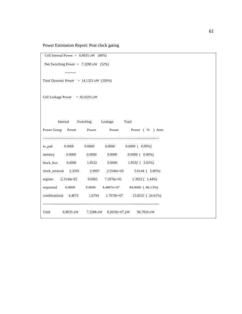
61
Power Estimation Report: Post clock gating
Cell Internal Power = 6.8035 uW (48%)
Net Switching Power = 7.3288 uW (52%)
---------
Total Dynamic Power = 14.1323 uW (100%)
Cell Leakage Power = 82.6593 uW
Internal Switching Leakage Total
Power Group Power Power Power Power ( % ) Attrs
--------------------------------------------------------------------------------------------------
io_pad 0.0000 0.0000 0.0000 0.0000 ( 0.00%)
memory 0.0000 0.0000 0.0000 0.0000 ( 0.00%)
black_box 0.0000 1.9532 0.0000 1.9532 ( 2.02%)
clock_network 2.3593 2.9997 2.5546e+05 5.6144 ( 5.80%)
register -2.3144e-02 0.6965 7.1876e+05 1.3922 ( 1.44%)
sequential 0.0000 0.0000 6.4007e+07 64.0066 ( 66.13%)
combinational 4.4673 1.6794 1.7678e+07 23.8252 ( 24.61%)
--------------------------------------------------------------------------------------------------
Total 6.8035 uW 7.3288 uW 8.2659e+07 pW 96.7916 uW

62
Power Estimation Report: Post Multi VDD Multi-Vt addition (Final stage)
Cell Internal Power = -4.1149 uW (-139%)
Net Switching Power = 7.0476 uW (240%)
---------
Total Dynamic Power = 2.9327 uW (100%)
Cell Leakage Power = 10.5436 uW
Leakage power with reduced spread = 0
Internal Switching Leakage Total
Power Group Power Power Power Power ( % ) Attrs
--------------------------------------------------------------------------------------------------
io_pad 0.0000 0.0000 0.0000 0.0000 ( 0.00%)
memory 0.0000 0.0000 0.0000 0.0000 ( 0.00%)
black_box 0.0000 1.8331 0.0000 1.8331 ( 13.60%)
clock_network 2.3924 2.8736 4.8312e+04 5.3143 ( 39.43%)
register -1.0163e+01 0.7159 7.8091e+04 -9.3693e+00
( -69.52%)
sequential 0.0000 0.0000 6.4454e+06 6.4454 ( 47.83%)
combinational 3.6559 1.6251 3.9718e+06 9.2529 ( 68.66%)
--------------------------------------------------------------------------------------------------
Total -4.1149e+00 uW 7.0476 uW 1.0544e+07 pW 13.4763 uW

63
Appendix C: Examples and Key commands
Example of resource sharing HDL [1]
always@(*)
// or can be written more strictly as
// always@(a or b or c or d or sel)
begin
If (sel)
result = a*b;
else
result = c*d;
end
// This creates only one instance of the multiplier, therefore contributes to saving dynamic power.
Example of typical HDL code written to insert fine grain clock gating
RTL for the design to be clock gated before synthesis
module dff_rtl(d, clk, cg_en, resetn, q);
input [3:0] d;
input clk, cg_en, resetn;
output reg [3:0] q;
always@(posedge clk or negedge resetn)
begin
if(~resetn)
begin
q <= 4'b0000;
end
else if(cg_en) // one has to add this enable for power
compiler to identify it as cg opportunity
begin
q <= d;
end
end
endmodule
Synthesized Gate Netlist -
module SNPS_CLOCK_GATE_HIGH_dff_rtl ( CLK,
EN, ENCLK, TE );
input CLK, EN, TE;
output ENCLK;
CGLPPRX2 latch ( .CLK(CLK), .EN(EN), .SE(TE),
.GCLK(ENCLK) ); // CGLPPRX2 is library cell name
endmodule
module dff_rtl ( d, clk, cg_en, resetn, q );
input [3:0] d;
output [3:0] q;
input clk, cg_en, resetn;
wire net19;
SNPS_CLOCK_GATE_HIGH_dff_rtl clk_gate_q_reg (
.CLK(clk), .EN(cg_en), .ENCLK(
net19), .TE(1'b0) );
DFFARX1 \q_reg[3] ( .D(d[3]), .CLK(net19),
.RSTB(resetn), .Q(q[3]) );
DFFARX1 \q_reg[2] ( .D(d[2]), .CLK(net19),
.RSTB(resetn), .Q(q[2]) );
DFFARX1 \q_reg[1] ( .D(d[1]), .CLK(net19),
.RSTB(resetn), .Q(q[1]) );
DFFARX1 \q_reg[0] ( .D(d[0]), .CLK(net19),
.RSTB(resetn), .Q(q[0]) );
endmodule

64
Synopsys report power command
Usage: report_power # display power report
[-net] (report power consumption of nets)
[-cell] (report power consumption of cells)
[-groups <cell_type1 cell_type2 ...>]
(report power of cells on specified set of cell types: io_pad, memory, black box, clock_network,
register, sequential, combinational)
[-only <cell_or_net_list>]
(report power only for these nets or cells)
[-cumulative] (report cumulative fanin/fanout power for cells/nets)
[-flat] (report all leaf-level cells or nets)
[-exclude_boundary_nets]
(exclude boundary nets; Note this flag is obsolete)
[-include_input_nets] (include primary input port nets)
[-analysis_effort <effort_level>]
(power analysis effort: low | medium | high)
[-verbose] (verbose power reporting)
[-nworst <number>] (max number of nets or cells to report:
Value >= 0)
[-sort_mode <mode>] (sort cells/nets by: name, cell_leakage_power, cell_internal_power, net_switching_power,
dynamic_power, net_toggle_rate, total_net_load, net_static_probability, cumulative_fanout, cumulative_fanin)
[-histogram] (display a histogram of net/cell info)
[-exclude_leq <le_val>]
(omit data-values less than or equal to <le_val> from histogram:
Value >= 0)
[-exclude_geq <ge_val>]
(omit data-values greater than or equal to <ge_val> from histogram:
Value >= 0)
[-nosplit] (do not split lines when fields overflow)

65
[-hierarchy] (report power consumption hierarchically)
[-levels <number>] (number of levels of hierarchy to be reported:
Value >= 0)
[-scenarios { scenario_name1 scenario_name2 ... }]
(report power on specifed set of scenarios, skip on inactive scenario(s))

66
Appendix D: Glossary
STA : Static timing analysis
SoC : System on Chip
FSM : Finite state machine
Vt : Threshold voltage
LVT : Low threshold voltage
SVT : Nominal threshold voltage
HVT : High threshold voltage
ASIC : Application specific integrated circuit
UPF : Unified Power format
FPGA : Field programmable gate array
SAIF : Switching activity interchange format
MVRC : Multi Voltage design rule check
MV : Multi voltage
CMOS : Complementary metal oxide semiconductor
DIBL : Drain induced barrier lowering leakage
HDL : Hardware description language
RTL : Register transfer language
Vt : Threshold Voltage
PLL : Phase locked loop
DFT : Design for testability
DDR : Dual data rate memory
UART : Universal asynchronous receiver transmitter
DRC : Design rule check

67
References
[1] Chandra, Rakesh and Bhaskar J. - An ASIC Low Power Primer: Analysis, Techniques and
Specification, Publisher – Springer, Publication Date 31 Oct 2012, “Chapter 6: Architectural
Techniques for Low Power”
[2] Chandra, Rakesh and Bhaskar J. - An ASIC Low Power Primer: Analysis, Techniques and
Specification, Publisher – Springer, Publication Date 31 Oct 2012, “Chapter 7: Low Power
Implementation Techniques”
[3] SpyGlass Power, The complete solution for power optimization at RTL, 23 April 2014
http://www.atrenta.com/products/spyglass-power.htm5
[4] Synopsys Design Compiler User Manual - Version G-2012.06-SP3 for RHEL32 -- Oct 23,
2012 http://www.synopsys.com/Tools/Implementation/RTLSynthesis/Pages/default.aspx. 23
April 2014
[5] AMBER SoC System open source org, 10 February 2014,
http://opencores.org/project,amber
[6] Chandra, Rakesh and Bhaskar J. - An ASIC Low Power Primer: Analysis, Techniques and
Specification, Publisher – Springer, Publication Date 31 Oct 2012, “Chapter 1: Introduction”
[7] Synopsys 90 nm technology library, 10 February 2014,
http://www.synopsys.com/Community/UniversityProgram/Pages/Library.aspx

68
[8] Chandra, Rakesh and Bhaskar J. - An ASIC Low Power Primer: Analysis, Techniques and
Specification, Publisher – Springer, Publication Date 31 Oct 2012, “chapter 5”
[9] Amber processor, 10 February 2014,
http://opencores.org/project,amber
[10] Power estimation tutorial, 9 October 2013,
http://www.tkt.cs.tut.fi/tools/public/tutorials/synopsys/pwr_est/gspe.html
[11] Technical Tutorial: “Low Power Design, Verification, and Implementation with IEEE
1801™ UPF™”, 10 May 2014
http://videos.accellera.org/upflowpower/upf38msn6y9/index.html
[12] MV verification, 23 April 2014,
http://www.synopsys.com/Tools/Verification/LowPowerVerification/Pages/MVSIM.aspx
#sthash.MFUzL6mz.dpuf
[13] Reducing Power with Advanced Clock Tree Synthesis and Optimization, 23 April 2013,
http://www.low-powerdesign.com/article_narayanan_CTS.htm
[14] Dhrystone MIPS benchmark, 23 April 2013,
http://en.wikipedia.org/wiki/Dhrystone

69
[15] Synopsys formality solution, 23 April 2013
http://www.synopsys.com/Tools/Verification/FormalEquivalence/Pages/Formality.aspx