implementation, verification and synthesis of the gigabit
TRANSCRIPT
Retrospective Theses and Dissertations Iowa State University Capstones, Theses and Dissertations
1-1-2000
Implementation, verification and synthesis of the Gigabit Ethernet Implementation, verification and synthesis of the Gigabit Ethernet
1000BASE-T Physical Coding Sublayer 1000BASE-T Physical Coding Sublayer
Sher-Li Chew Iowa State University
Follow this and additional works at: https://lib.dr.iastate.edu/rtd
Recommended Citation Recommended Citation Chew, Sher-Li, "Implementation, verification and synthesis of the Gigabit Ethernet 1000BASE-T Physical Coding Sublayer" (2000). Retrospective Theses and Dissertations. 21126. https://lib.dr.iastate.edu/rtd/21126
This Thesis is brought to you for free and open access by the Iowa State University Capstones, Theses and Dissertations at Iowa State University Digital Repository. It has been accepted for inclusion in Retrospective Theses and Dissertations by an authorized administrator of Iowa State University Digital Repository. For more information, please contact [email protected].

Implementation, verification and synthesis of the Gigabit Ethernet
1 000BASE-T Physical Coding Sublayer
by
Sher-Li Chew
A thesis submitted to the graduate faculty
in partial fulfillment of the requirement for the degree of
MASTER OF SCIENCE
Major: Computer Engineering
Major Professor: Marwan Hassoun
Iowa State University
Ames, Iowa
2000
ii
Graduate College
Iowa State University
This is to certify that Master's thesis of
Sher-Li Chew
has met the thesis requirements of Iowa State University
Signatures have been redacted for privacy

iii
TABLE OF CONTENTS
LIST OF FIGURES ............................................................................................................................. V
LIST OF TABLES ............................................................................................................................. vii
ABSTRACT ....................................................................................................................................... viii
1 INTRODUCTION ............................................................................................................................. 1 1.1 Ethernet Overview ........................................................................................................................ 1
1.2 Why Gigabit Ethernet? ................................................................................................................. 2
1.3 Category 5 Unshielded Twisted Pair Copper Cable ..................................................................... 2
1.4 Carrier Sense Multiple Access with Collision Detection (CSMA/CD) ........................................ 3
1.5 Functional Modeling and Simulation ........................................................................................... 4
1.6 Organization of Thesis ................................................................................................................. 6
2 PHYSICAL CODIING SUBLAYER SPECIFICATIONS AND IMPLEMENTATION ........... 8 2.1 Introduction .................................................................................................................................. 8
2.2 l000BASE-T System Overview ................................................................................................... 8
2.2.1 Physical Coding Sublayer (PCS) Role ................................................................................. 12
2.2.2 Physical Coding Sublayer (PCS) and Physical Medium Attachment (PMA) Interfaces ..... 13
2.2.3 PCS and GMII Interfaces ..................................................................................................... 15
2.3 Basic Coding Theory Overview ................................................................................................. 17
2.3.1 Scrambling Basics ................................................................................................................ 17
2.3.2 Descrambling Basics ............................................................................................................ 20
2.3.3 Convolutional Codes ............................................................................................................ 22
2.4 l000BASE-T Coding System ..................................................................................................... 22
2.4.1 Selecting the Channel Symbols ........................................................................................... 22
2.4.2 Defining the 4D/P AM5 Structure ........................................................................................ 23
2.4.3 Trellis Structure ................................................................................................................... 24
2.4.4 The Master/Slave Scramblers employed ............................................................................. 26
2.5 Physical Coding Sublayer (PCS) Functions ............................................................................... 28
2.5.1 PCS Transmit Function ........................................................................................................ 29
2.5.2 PCS Data Transmission Enable Function ............................................................................ 33
2.5.3 PCS Carrier Sense Function ................................................................................................ 33
2.5.4 PCS Receive Function ......................................................................................................... 33 ·

iv
2.6 Conclusion .................................................................................................................................. 35
3 PCS TESTING AND SIMULATION RESULTS ........................................................................ 36
3.1 Introduction ................................................................................................................................ 36
3.2 PCS Top Level ........................................................................................................................... 36
3.3 PCS Transmit ............................................................................................................................. 39
3.4 PCS Data Transmission Enable .................................................................................................. 40
3.5 PCS Carrier Sense ...................................................................................................................... 41
3.6 PCS Receive ............................................................................................................................... 42
3.7 Intermediate Parameters ............................................................................................................. 44
3.8 Conclusion .................................................................................................................................. 47
4 SYNTHESIS AND SIMULATION RESULTS ............................................................................ 48
4.1 Introduction ................................................................................................................................ 48
4.2 Synthesis Overview .................................................................................................................... 48
4.3 Synthesis Results for l.4µm CMOS Library .............................................................................. 52
4.4 Synthesis Results for 0.35µm CMOS Library ............................................................................ 53
4.5 Gate-Level Simulation Results ................................................................................................... 62
4.6 Conclusion .................................................................................................................................. 65
5 CONCLUSIONS ............................................................................................................................. 66
5.1 Thesis Conclusion ...................................................................................................................... 66
5.2 Future Work ............................................................................................................................... 67
APPENDIX A: BIT-TO-SYMBOL MAPPING TABLE ................................................................ 68
APPENDIX B: STATE DIAGRAMS ............................................................................................... 76
APPENDIX C: SYNOPSYS SCRIP'f FILES .................................................................................. 81
APPENDIX D: PCS SIGNALS DEFINITIONS ............................................................................. 86
REFERENCES ................................................................................................................................... 92

V
LIST OF FIGURES
Figure 1 Digital design methodology [27] ............................................................................................. 5
Figure 2 IIDL flows ............................................................................................................................... 5
Figure 3 lOOOBASE-X (802.3z) and lO00BASE-T (802.3ab) (9) ......................................................... 9
Figure 4 lOOOBASE-T PHY relationship to the ISO Open Systems Interconnection (OSI) [16] ....... 10
Figure 5 Cabling topology [16) ............................................................................................................ ll
Figure 6 Bit-to-symbol and symbol-to-bit conversion ......................................................................... 12
Figure 7 Data transmission frame [16) ................................................................................................. 13
Figure 8 PCS and PMA interfaces ....................................................................................................... 14
Figure 9 Frame transmission flow diagram .......................................................................................... 16
Figure 10 PCS and GMII interfaces [ 16] ............................................................................................. 16
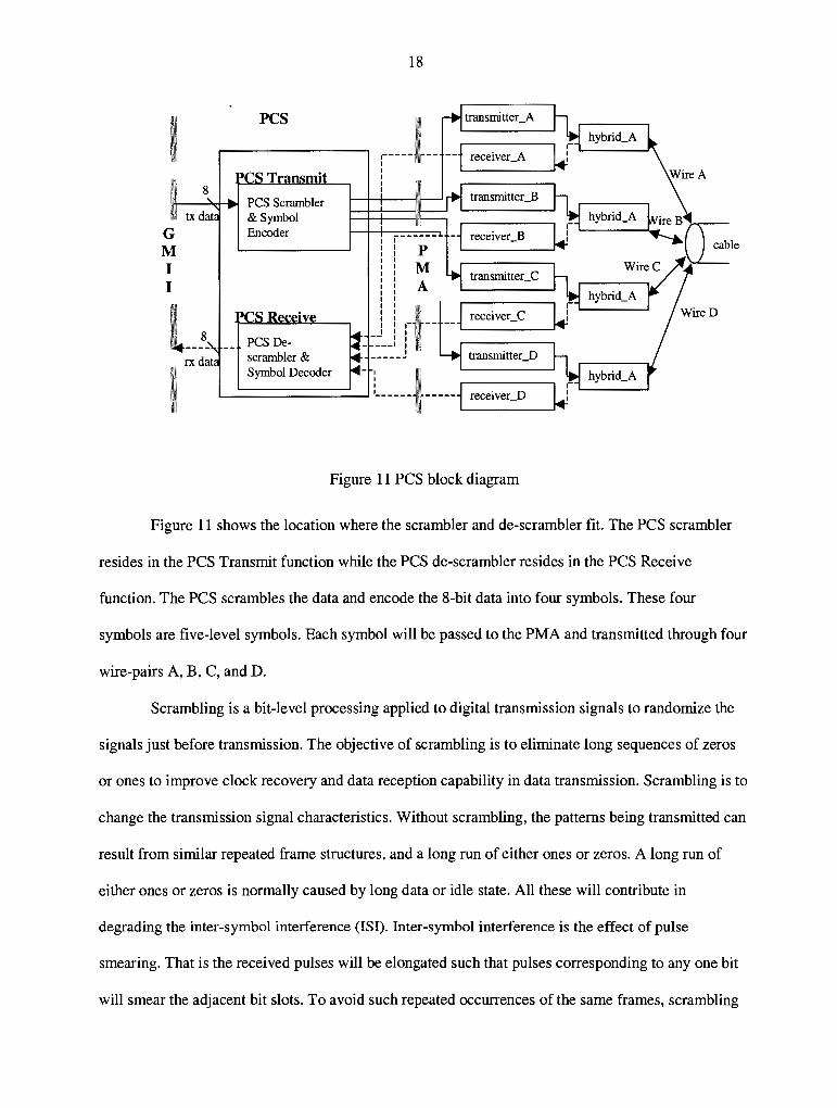
Figure 11 PCS block diagram .............................................................................................................. 18
Figure 12 Frequency spectrum for repetitive signals [23] ................................................................... 19
Figure 13 Frequency content without spread spectrum [23] ................................................................ 19
Figure 14 Frequency content with spread spectrum [23] ..................................................................... 20
Figure 15 3-bit Linear Feedback Shift Register (LFSR) ...................................................................... 21
Figure 16 Trellis Encoder ..................................................................................................................... 25
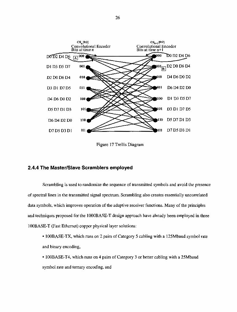
Figure 17 Trellis Diagram .................................................................................................................... 26
Figure 18 Side-stream scrambler for Master and Slave [16] ............................................................... 27
Figure 19 PCS functions [16) ............................................................................................................... 28
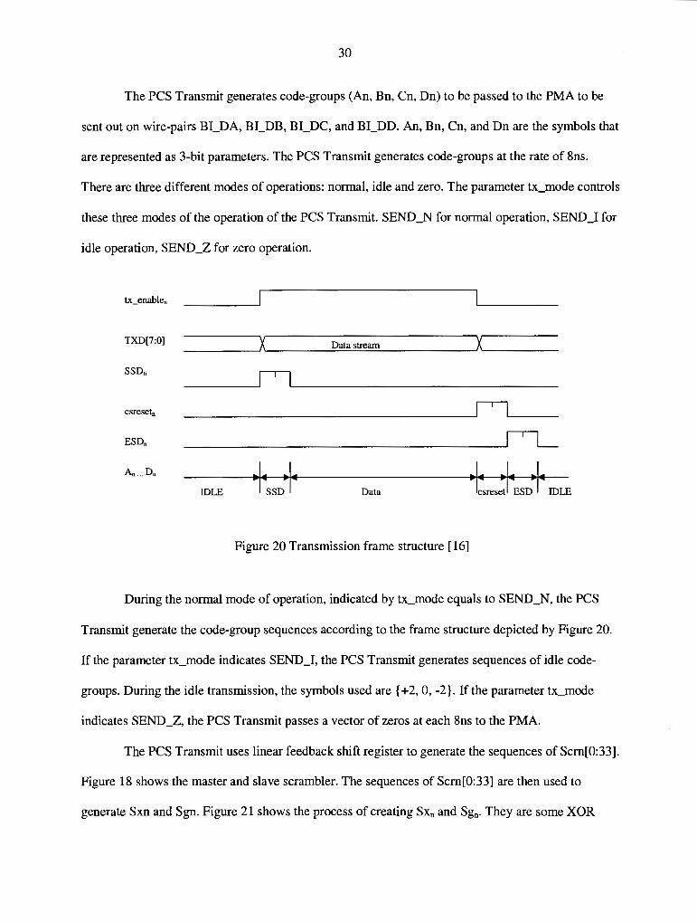
Figure 20 Transmission frame structure [ 16] ....................................................................................... 30
Figure 21 Generation of Sxn and Sgn from the scrambler .................................................................... 31
Figure 22 Processes of generating code-group An, Bn, Cn and Dn••·············· .. ······································ 32 Figure 23 Scrambling and convolutional encoding .............................................................................. 32
Figure 24 Receive Function: Decoding of RXD[7:0] .......................................................................... 35
Figure 25 Hierarchy of the top level PCS ............................................................................................ 37
Figure 26 Simulation results for PCS top level.. .................................................................................. 38
Figure 27 Simulation results for PCS Transmit function ..................................................................... 39
Figure 28 Simulation results for PCS Data Transmission Enable function ......................................... 41
Figure 29 Simulation results for PCS Carrier Sense function .............................................................. 42
Figure 30 Simulation results for PCS Receive function ...................................................................... 43
Figure 31 Encoding flow diagram ........................................................................................................ 44

vi
Figure 32 Simulation results for parameters: Scr0 , Sg0 , Sx0 and Syn ................................................... 45
Figure 33 Simulation results for parameters: Sen, SnAn, SnBn, SnCn and SnDn .................................. 45
Figure 34 Simulation results for parameters: Sdn, TA, TB, TC and TD .............................................. 46
Figure 35 Simulation results for parameters: A, B, C and D ............................................................... 46
Figure 36 Synthesis steps [41] ............................................................................................................. 49
Figure 37 Sample Syn op sys timing report ........................................................................................... 51
Figure 38 Hierarchical synthesis: transmitter timing results for 0.35µm CMOS ................................ 56
Figure 39 Hierarchy synthesis: receiver timing results for 0.35µm CMOS ......................................... 57
Figure 40 Hierarchical synthesis: transmitter area results for 0.35µm CMOS .................................... 58
Figure 41 Hierarchy synthesis: receiver area results for 0.35µm CMOS ............................................ 58
Figure 42 Flatten synthesis: transmitter timing results for 0.35µm CMOS ......................................... 59
Figure 43 Flatten synthesis: receiver timing results for 0.35µm CMOS .............................................. 60
Figure 44 Flatten synthesis: transmitter area results for 0.35µm CMOS ............................................. 61
Figure 45 Flatten synthesis: receiver area results for 0.35µm CMOS ................................................. 61
Figure 46 Gate-level simulation results for top-level function ............................................................ 62
Figure 47 Gate-level simulation results for transmit function ............................................................. 63
Figure 48 Gate-level simulation results for data transmission enable function ................................... 63
Figure 49 Gate-level simulation results for carrier sense function ...................................................... 64
Figure 50 Gate-level simulation results for receive function ............................................................... 64
Vll
LIST OF TABLES
Table 1 Different categories of UTP (Unshielded Twisted Pairs) [14) .................................................. 3
Table 2 Subset mapping ....................................................................................................................... 24
Table 3 Synthesis area and area in µm2 for 1.4µm CMOS .................................................................. 52
Table 4 Synthesis results comparison for 1.4µm CMOS ..................................................................... 52
Table 5 Synthesis results summary for 1.4µm CMOS ......................................................................... 52
Table 6 Synthesis area and area in µm2 for 0.35µm CMOS ................................................................ 54
Table 7 Synthesis results comparison for 0.35µm CMOS ................................................................... 54
Table 8 Synthesis result summary for 0.35µm CMOS ........................................................................ 54

Vlll
ABSTRACT
To meet the increasing demand for additional bandwidth requirements, high-speed
connections are required to reduce traffic bottlenecks and improve performance on network systems.
Gigabit Ethernet offers a cost-effective solution that is compatible with existing technologies to
protect large investments in network infrastructure. IEEE standard 802.3ab lOOOBASE-T (Gigabit
Ethernet) physical layer standard offers this solution which upgrades networks to lO00Mbps data
rates while maintaining the simplicity and manageability of the existing Ethernet networks, just as
lO0BASE-T Ethernet extended lOBASE-T Ethernet networks. The lOO0BASE-T physical layer
standard providing 1 Gbps Ethernet signal transmission over four pairs of category 5 unshielded
twisted pair (UTP) cable using the 5-level coding scheme.
The Physical Coding Sublayer (PCS) of IEEE 802.3ab 1 OO0BASE-T physical layer was
developed and implemented. The behavioral modeling, functional modeling and simulation were
done using Verilog HDL®. Then, the PCS was synthesized using two process libraries: 0.35µm
CMOS and 1.4µm CMOS. Two synthesis techniques, hierarchical optimization and hierarchical-
flattening optimization, were explored to compare the area and timing tradeoffs between them The
automation of the synthesis was accomplished with the creation of synthesis script files. With these
script files, the PCS can be synthesized automatically with any target library desired.

1
1 INTRODUCTION
1.1 Ethernet Overview
Ethernet is a reliable and popular networking technology that has evolved from low
bandwidth coaxial, to lOBaseT, lO0BaseT and now to the development of gigabit technology.
Ethernet is a type of network cabling and signaling specifications. It allows communications between
computers. In 1985, the Institute of Electrical and Electronics Engineers (IEEE) published the first set
of Ethernet standards IEEE 802.3 Carrier Sense Multiple Access with Collision Detection
(CSMA/CD) Access method and Physical Layer Specifications. Shortly after the publication of that
standard, International Standards Organization (ISO) adopted this standard and specified the
international standard number IS88023. This enabled the Ethernet technology to become the most
widely used method for Local Area Networks (LANs) connection [22].
In Ethernet technology, the l0BASE-T has been the most commonly used technology since
the 1980s. As network traffic increased, the bandwidth of lOMbps provided by the lOBaseT was no
longer sufficient. In 1995, the emergence of Fast Ethernet (lO0BASE-T) provided a smooth upgrade
from lOMbps to lOOMbps. Among the LAN technologies, Fast Ethernet (lO0BASE-T) is the most
commonly used technology. Ethernet products dominate the market today by 87% and are likely to do
so for the future [22]. As the demand for more bandwidth increases, it creates a distinct need for a
higher-speed network solution. As an extension of current Fast Ethernet technology, Gigabit Ethernet
(lO00BASE-T) which runs over the existing UTP is compatible with the most widely deployed
networking infrastructure [22].
Unlike Token Ring and ATM (Asynchronous Transfer Mode), Gigabit Ethernet solves the
bandwidth predicament without requiring costly cabling changes [19]. The performance and speed

2
advantages of Gigabit Ethernet technology, combined with the ease of migration through the use of
the existing network infrastructure, offer compelling motivation for adopting lOO0BASE-T solutions.
1.2 Why Gigabit Ethernet?
There are several factors that contribute to the increasing demand for network bandwidth
higher than lOOMbps delivered by Fast Ethernet: The exponential growth of the intranet and internet
traffic; The increasing of the file sizes caused by the increasing complexity of desktop publishing
high-resolution imaging and multimedia applications; The booming of the interactive applications
like desktop video conferencing, web-based computer training and net radio/music channels.
Compared to the alternative solutions for high-speed networking, such as ATM and Token Ring,
Gigabit Ethernet offers the advantage of using protocols directly compatible with currently
implemented Ethernet standards. Thus, it makes the smooth, low-cost and incremental migrations
from Ethernet and Fast Ethernet to Gigabit Ethernet possible [9].
Fast Ethernet's success can be attributed largely to its compatibility with lOMbps Ethernet. It
left as much of the original Ethernet specification as unchanged as possible. That was an essential
strategy for making Gigabit Ethernet successful as well [9].
1.3 Category 5 Unshielded Twisted Pair Copper Cable
l0Base-T networks use Category 3 or higher l00ohm UTP cables. UTP cabling categories
are defined in the Telecommunications Industry Association and the Electronic Industry Association
cabling standards (TIA/EIA-568A) [16]. Currently, there are 5 categories for Horizontal UTP cable.
Cabling categories are also documented in the Canadian equivalent standard (CSA T529), as well as

3
the international standard (ISO/IEC 11801). Categories are distinguished by the quality of the cable,
or the speed at which reliable communication can take place. In appearance, all UTP cables look
similar to most telephone wire [14]. Table 1 lists all five UTP cabling categories and the performance
standards associated with each.
Table 1 Different categories of UTP (Unshielded Twisted Pairs) [14]
UTP Cate2ory Rated Performance Applications Category 1 No performance Used in some older telephone systems (cat 1) criteria Category 2 1MHz Used for telephone wiring (cat 2) Category 3 16MHz Used for lOBASE-T-widely deployed, (cat 3) especially in older installations Category 4 20MHz Used for lOBASE-T and Token Ring (cat 4) Category 5 100MHz Used for lOBASE-T, lO0BASE-T(Fast Ethernet) (cat 5) and other high speed network technologies
1.4 Carrier Sense Multiple Access with Collision Detection (CSMA/CD)
Carrier Sense Multiple Access/Collision Detection (CSMA/CD) is one of the many
algorithms for allocating a multiple-accessed channel. Carrier Sense means that network stations with
data to transmit should first listen to determine if another station is sending data. Multiple Access
means that Ethernet provides a number of stations the chance to transmit on the single cable.
Collision Detection refers to the detection of simultaneous transmissions by more than 1 station.
Stations can tell if the channel is in use before trying to use it. If the channel is sensed as busy, no
station will attempt to use it until the channel goes idle. There are basically three states for a
CSMA/CD: contention, transmission and idle. Any transmission will be aborted as soon as a collision
is detected. For example, if two stations detect idle at the same time and begin to transmit
simultaneously, both will detect collision immediately and stop transmitting.

4
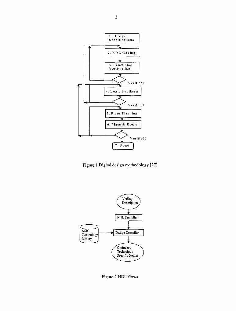
1.5 Functional Modeling and Simulation
Verilog Hardware Description Language (HDL) was used to model the Physical Coding
Sublayer functionality. Synopsys was used to generate and optimize the Verilog HDL description into
gate-level equivalent. This section introduces the concepts of Hardware Description Language and
design methodology [27].
Today, Hardware Description Languages (HDLs) are used widely by digital integrated circuit
designers to describe the functions and behavior of the discrete electronic systems. The functionality
of the design can be verified early in the design process. There are different modem tools for digital
systems. This includes synthesis, floor planning, placement and routing. The common design flow is
shown in Figure 1. Synopsys offers a HDL compiler that can automatically translate Verilog language
to Synopsys gate-level format in a target technology. The gate-level format can then be optimized and
mapped to a specific ASIC technology library by Design Compiler. Figure 2 shows the function of
the Design Compiler.
The design methodology that was being used for this implementation of the Physical Coding
Sublayer is shown in Figure 1. First, the PCS was modeled in Verilog HDL. The Verilog HDL
contains the structural and functional elements. It's simulated in Verilog-XL to verify its functional
correctness using the corresponding test benches. The Synopsys HDL Compiler converts the HDL
into gate-level. The optimized gates, with the timing constraints, were generated using the specific
ASIC (Application Specific Integrated Circuits) technology using Synopsys Design Compiler. Two
synthesis techniques, hierarchical optimization and hierarchical-flattening optimization, were used to
explore the trade-off of area and timing between them. The automation of the synthesis was
accomplished with the creation of synthesis script files. With these script files, the PCS can be
synthesized automatically with any target library desired.
5
I.Design Specifications
2. HDL Coding
3. Functional Verification
Verified?
4. Logic Synthesis
Verified?
5. Floor Planning
6. Place & Route
Verified?
7. Done
Figure 1 Digital design methodology [27]
ASIC Technology Library
Verilog Description
HDL Compiler
Design Compiler
Figure 2 HDL flows

6
Design Compiler can generate the gate-level description in Verilog HDL format and the delay
information of the gates as Standard Delay Format (SDF) file. This gate-level Verilog HDL
description is in netlist-style description where it describes the design using the corresponding leaf-
level cells of the specific ASIC technology library. Both of the gate-level Verilog HDL and SDF were
then simulated using Verilog-XL compiler. The same original test benches from the previous
behavioral verification can be used because the module and port definitions are preserved through the
translation and optimization processes. The output of the gate-level simulation was compared to the
original output from the Verilog description simulation to ensure correct implementation.
The output of the gate-level simulations contains the corresponding timing and delay as
specified in the Standard Delay Format file. When the design did not meet the timing specification,
the functional and behavioral description have to be modified and the step 1 through step 4 in Figure
1 have to be repeated until the timing constraints are met.
1.6 Organization of Thesis
This thesis aims to implement the Physical Coding Sublayer of the l000BASE-T IEEE
standard 802.3ab. The behavioral modeling, functional modeling and simulation were done using
Verilog HDL®. Then, the PCS was synthesized using two process libraries: 0.35µm CMOS and
1.4µm CMOS. Two synthesis techniques, hierarchical optimization and hierarchical-flattening
optimization, were explored to compare the area and timing tradeoffs between them. The automation
of the synthesis was accomplished with the creation of synthesis script files. With these script files,
the PCS can be synthesized automatically with any target library desired. The gate-level was verified
to meet the functionality and timing as specified by the IEEE standard.
7
This work has tremendous commercial and industrial value because it is the leading edge
technology that will shape the future Gigabit Ethernet technology. According to In-Stat, a national
market research firm, the total opportunity for the Fast Ethernet and Gigabit Ethernet IC market will
grow to nearly $1.9 billion in 1999, and continue that growth throughout the forecast period, hitting
$2.7 billion in 2003. By 2004, it is expected that Gigabit Ethernet will be 59.2 percent of all Ethernet
Network Interface Cards (NICs) shipped. (In-Stat, Networking LAN Service, report number
LN9914NC) [19].
The thesis is organized as follows: Chapter two presents the specifications of the Physical
Coding Sublayer of IOO0BASE-T. Simulation results for the Physical Coding Sublayer (PCS) are
shown in chapter three. Synthesis results and discussion are presented in chapter four. Finally,
conclusion is presented in chapter five.
There are three appendices: Appendix A contains the bit-to-symbol mapping table, Appendix
B contains the state machines for different functions of the PCS, and Appendix C contains the scripts
for Synopsys.

8
2 PHYSICAL CODIING SUBLAYER SPECIFICATIONS AND IMPLEMENTATION
2.1 Introduction
In this chapter, the IEEE standard 802.3ab (lO00BASE-T) is described. In section 2.2, the
top-level system overview is explained. The main role of the PCS is highlighted. The interface of the
Physical Coding Sublayer (PCS) with other layers is described. The two layers that interface with the
PCS are the Gigabit Media Independent Interface (GMII) and the Physical Medium Attachment
(PMA). In the next section, the basic coding theory is introduced before the description of the
lO00BASE-T coding system is explored. Finally, the functions of the PCS are introduced.
2.2 1 000BASE-T System Overview
The 1 000BASE-T is one of the specifications of Gigabit Ethernet family by IEEE. The
lO00BASE-T is the standard IEEE 802.3ab that allows the data transfer over CAT-5 copper wire. It
provides half-duplex (CSMNCD) and full-duplex lO00Mb/s Ethernet service. The lO00BASE-T
PHY (Physical Layer) consists of the Physical Coding Sublayer (PCS), the Physical Medium
Attachment (PMA) and baseband medium specifications [16].
The lO00BASE-T system objectives are as follows:
• Provide lOOOMbps full duplex link between nodes
• Support existing largely installed cable, CAT 5 Unshielded Twisted Pairs (UTP) cable.
• Operate with a bit error rate of :s; 10-10
• Meet or exceed FCC Class NCISPR
• Support CSMNCD MAC

9
• Comply with the GMII Specifications
• Support lO00Mbps repeater
• Support Auto-Negotiation
IEEE P802.3z standard specifies 1000-Mbps-Ethemet operation over fiber optic cable, while
the IEEE P802.3ab standard enables 1000-Mbps operation over Category 5 (CAT-5) or higher rated
copper cable. There are four physical layer signaling systems: lO00BASE-SX (short wavelength
fiber), lO00BASE-LX (long wavelength fiber), lOOOBASE-CX (short run copper) and l000BASE-T
(100-meter, four-pair Category 5 UTP). Figure 3 shows the location where the IEEE 802.3ab fits into
[9].
Media Access Control (MAC) Full Duplex/Half Duplex
lOOOBASE-X 8b/10b Encoder/Decoder
lOOOBASE-SX lOOOBASE-SX lOOOBASE-SX Transceiver Transceiver Transceiver
Figure 3 lO00BASE-X (802.3z) and lO00BASE-T (802.3ab) [9]
lO0BASE-TX achieves lOOMbps by using 4B5B (conversion of 4 bits to 5 bits) coding to
send three-level binary encoded symbols across the cable at 125Mbaud. lOOOBASE-TX uses the
8B10B (conversion of 8 bits to 10 bits). Gigabit Ethernet over copper (l000BASE-T) uses four pairs
of two twisted cables (one to transmit and one to receive) to transmit at a 125-Mbaud rate with a five-
level coding scheme for each link. Because lOO0BASE-T sends and receives simultaneously on each
10
pair, the combination of five-level coding and four pairs allows lO00BASE-T to send one byte in
parallel at each signal pulse.
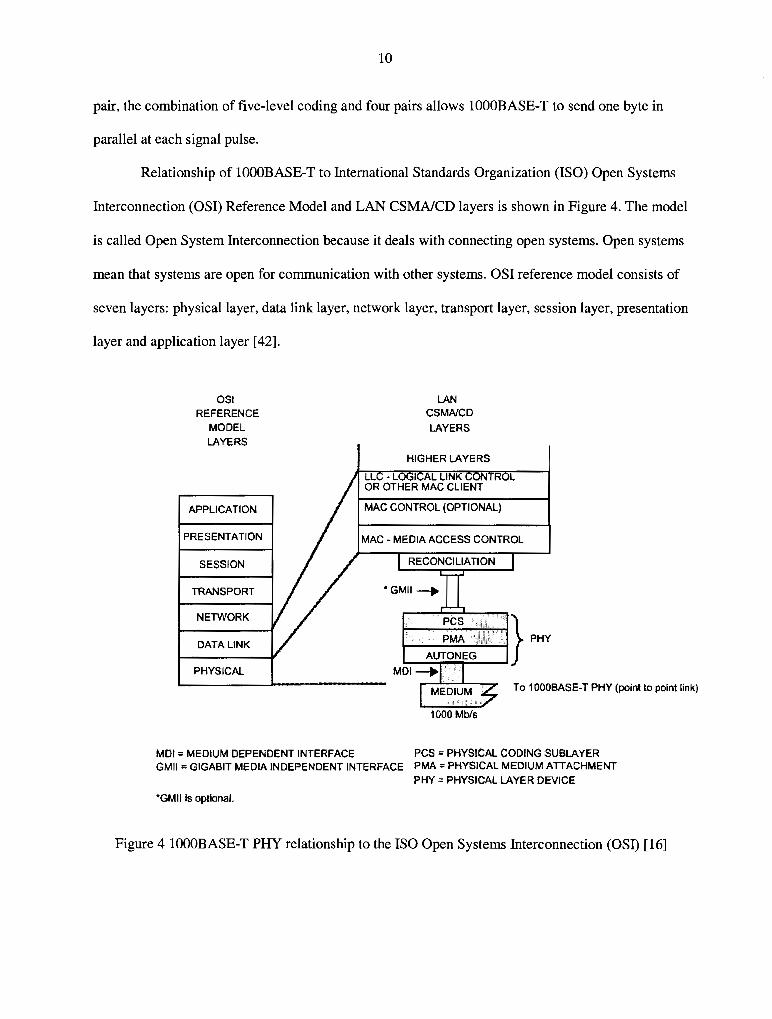
Relationship of lO00BASE-T to International Standards Organization (ISO) Open Systems
Interconnection (OSI) Reference Model and LAN CSMNCD layers is shown in Figure 4. The model
is called Open System Interconnection because it deals with connecting open systems. Open systems
mean that systems are open for communication with other systems. OSI reference model consists of
seven layers: physical layer, data link layer, network layer, transport layer, session layer, presentation
layer and application layer [42].
OSI REFERENCE
MODEL LAYERS
APPLICATION
PRESENTATION
SESSION
TRANSPORT
NETWORK
DATA LINK
PHYSICAL
LAN CSMNCD LAYERS
HIGHER LAYERS
OR OTHER MAC CLIENT
MAC CONTROL (OPTIONAL)
MAC - MEDIA ACCESS CONTROL
RECONCILIATION
To 1 OO0BASE-T PHY (point to point link)
1000 Mb/s
MDI= MEDIUM DEPENDENT INTERFACE PCS= PHYSICAL CODING SUBLAYER GMII = GIGABIT MEDIA INDEPENDENT INTERFACE PMA = PHYSICAL MEDIUM ATTACHMENT
PHY= PHYSICAL LAYER DEVICE
*GMII is optional.
Figure 4 lOOOBASE-T PHY relationship to the ISO Open Systems Interconnection (OSI) [16]

11
Cabling topology of the 1 000BASE-T is shown in Figure 5. Data transmission is over 4
twisted pairs. Each wire-pair achieves the data rate of 250 Mb/s. Therefore the total data rate is
lO00Mb/s. In half-duplex communication, data can travel in both directions, but not simultaneously.
However, full-duplex means that the data can travel in both directions at the same time. In order to
obtain full duplex operation, hybrids and cancellers are used. This allows the data to be transmitted
and received at the same time on the same wire-pairs. There are 4 wire-pairs, so the data is
transmitted as four-dimensional. Four-dimensional symbols can be regarded as a 4-tuple (An, Bn, Cn,
Dn), For each dimension, there are 5 levels of symbols being used, which are represented as 2, 1, 0, -1
or -2. In short, the transmission uses the 4D-P AM5 (four Dimensional, five Pulse Amplitude
Modulation) [16]. The 4D-PAM5 structure will be explained more in chapter 2.4 lOO0BASE-T
Coding System.
H H y y 250 Mb/s B B 250 Mb/s R R
I I D D
H H y y
250 Mb/s B B 250 Mb/s R R I I D D
H H y y B B 250 Mb/s R R
250 Mb/s
I I D D
H H y y B B 250 Mb/s R R
250 Mb/s
I I D D
Figure 5 Cabling topology [16]

12
2.2.1 Physical Coding Sublayer (PCS) Role
As the name of the Physical Coding Sublayer implies, its main function is the encoding and
decoding of the symbols. The PCS takes in 8-bit data from the Gigabit Media Independent Interface
(GMII). After the operation on the 8-bit data, it generates a 4-quinary symbol to The Physical
Medium Attachment (PMA).
The IO00BASE-T PCS resides between the Gigabit Media Independent Interface (GMII) and
The Physical Medium Attachment (PMA). The GMII and the PMA will be discussed in the following
sections. The PCS continuously generates code-groups to be transmitted over 4 wire-pairs. The
transmission technique being used is 4D-PAM5, which converts 8-bit data into four-quinary symbols.
4 quinary 8 bits Tx s~bols ...
\ ... \ \
PCS GMII PMA
\
\ \
8 bits Rx \
4 quinary symbols
Figure 6 Bit-to-symbol and symbol-to-bit conversion
The frame of the transmission is shown in Figure 7. When the tx_enable (transmit enable) is
asserted, two bytes of code-groups, SSD 1 and SSD2, are sent. Immediately after that, the 8-bit
transmit data stream (TXD[7:0]) from the GMII is being sent. At the end of the frame, tx_enable is
de-asserted. Upon that, two bytes of code-groups, Convolutional State Reset (CSReset) are sent. After
that, ESD 1 and ESD2 are sent. Between frames, IDLE mode is being transmitted. IDLE mode differs
from DAT A mode where the idle code-groups only consist of { 2, 0, -2} while data code-groups
consist of {2, 1, 0, -1, -2}.
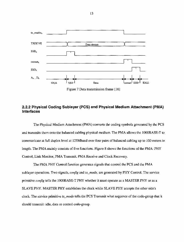
13
tx_enable0
TXD[7:0] ----~x~ ____ D_a_ta_s_tr_ea_m ______ ~x~----SSDn
csreset0
ESDn
IDLE Data
Figure 7 Data transmission frame [16]
2.2.2 Physical Coding Sublayer (PCS) and Physical Medium Attachment (PMA) Interfaces
The Physical Medium Attachment (PMA) converts the coding symbols generated by the PCS
and transmits them onto the balanced cabling physical medium. The PMA allows the lO00BASE-T to
communicate at full duplex level at 125Mbaud over four pairs of balanced cabling up to 100 meters in
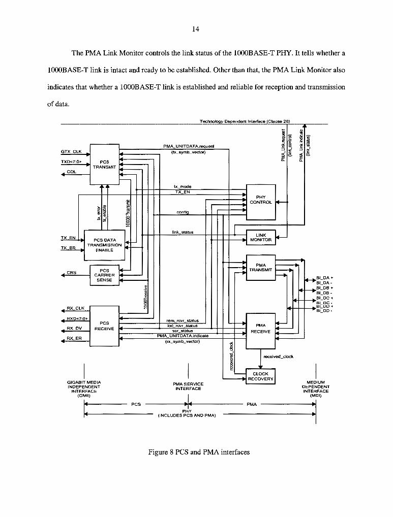
length. The PMA mainly consists of five functions. Figure 8 shows the functions of the PMA: PHY
Control, Link Monitor, PMA Transmit, PMA Receive and Clock Recovery.
The PMA PHY Control function generates signals that control the PCS and the PMA
sublayer operations. Two signals, con.fig and tx_mode, are generated by PHY Control. The service
primitive con.fig tells the lO00BASE-T PHY whether it must operate as a MASTER PHY or as a
SLAVE PHY. MASTER PHY establishes the clock while SLAVE PHY accepts the other side's
clock. The service primitive tx_mode tells the PCS Transmit what sequence of the code-group that it
should transmit: idle, data or control code-group.
14
The PMA Link Monitor controls the link status of the lO00BASE-T PHY. It tells whether a
lO00BASE-T link is intact and ready to be established. Other than that, the PMA Link Monitor also
indicates that whether a 1 0OOBASE-T link is established and reliable for reception and transmission
of data.
GTX CLK --TXD<7:0> PCS ·-- TRANSMIT : - COL +--
,.,
- Sl !!! ej I:!! lll, ., i is 15'
TX EN . PCS DATA - •-TX ER
TRANSMISSION •-- ENABLE
CRS PCS CARRIER
SENSE
RX CLK
RXD<7:0> - PCS RX DV RECEIVE -
_ RX ER
I GIGABIT MEDIA INDEPENDENT
INTERFACE (GMII)
1:
.._ : -
--, -, -
PCS
., .2: fl l:o 0
Technology Dependent Interface (Clause 28)
PMA_ UNITDATA.request (tx_symb_ vector}
tx mOde TX EN
confiq
link status
rem rcvr status loc rcvr status
scr status PMA ... UNITDATA.lndicate
(rx ... symb __ vector)
I PMASERVICE
INTERFACE
PHY (INCLUDES PCS AND PMA)
i 'g @'
! .,;_ :5 ~I g a
. . PHY - CONTROL ._ --I LINK r--;c: MONITOR
r=: PMA TRANSMIT =;-to
----+ I+-PMA RECEIVE -
""
' received_clock
i ,. !!? ---:i CLOCK
• 1RECOVERY
PMA
Figure 8 PCS and PMA interfaces
-
,. .~--;; "' ;a ., § :! ~' @., a
. -l+-+~I_D
BI .... D f---+~I_D
BI_D • BI_D - Bl D
BCD -B1_D
I MEDIUM
A+ A-B+ B· C+ C-u+ D•
DEPENDENT INTERFACE
(MDI)
:1

15
The PMA Transmit contains four independent transmitter wire-pairs: BI_DA, BI_DB,
BI_J;>C, and BI_DD. These fo-Ul' pairs of wire will sent out five-level pulse-amplitude modulated
signals (4D-PAM5). The voltages of+/- lv map the symbols of+/- 2, and the voltages of+/- 0.5v
map the symbols of +/-1.
2.2.3 PCS and GMII Interfaces
The PCS interfaces with the GMIT. The GMII is the interface between the PCS and the
Medium Access Control layer. Figure 4 shows the location where GMII resides in the Local Area
Network (LAN) Carrier Sense Multiple Access/Collision Detection (CSMA/CD) sublayers. The
GMII is designed to make the differences among the various media transparent to the MAC sublayer.
It provides media independence so that an identical media access controller may be used with any of
the copper and optical PHY types [16].
Data octets, TXD[7:0] are provided by the GMII to the PCS. The GMII provides the PCS
with the signal TX_EN (transmit enable). Figure 9 shows the flow diagram for the frame
transmission. When l0OOBASE-T is ready for transmission, the signal TX_EN will be asserted by the
GMII. When TX_EN is asserted, the PCS will switch from IDLE state to generating 2 frames of Start
of Stream Delimiter (SSD). Following that, the PCS will generate the corresponding data octets
TXD[7:0] frame to be transmitted according to the encoding rules. The PCS will be provided by the
GMII with the transmitting clock. Therefore, the code-groups are sent out synchronously with the
clock signal, GTX_CLK. When the GMII de-assert the signal TX_EN, the PCS will end the data
frame transmission by first sending out two Convolutional State Reset (CSReset) code-groups and
then two End of Stream Delimiters (ESDs). Then, the PCS returns back to the IDLE state.

PCS: IDLE
16
GMII asserts PCS: from TX_EN IDLEtoSSD
Ready for transmission
PCS: from CSResetto PCS: from GMII de-asserts ESD DATA to TX_EN
CSReset
Figure 9 Frame transmission flow diagram
GTX..CLK
G TXD<7:0>
TX,.EN
TX_ER
M - COL -
I _ CRS -- RX_CLI<
I . - RXD<7:0>
RXDV
RX ER -
GIGABIT MEDIA INDEPENDENT
INTERFACE (GMII)
--- p -;;
-C
s
Figure 10 PCS and GMII interfaces [16]
PCS transmit DATA(TXD)
Stop data transmission
The GMII will assert the signal TX_ER when there is error from the upper layer of the
network. Then, the PCS will finish up its current code-group generation and will start generating
xmit_error code-group on the next transmit clock. When that happens, the PCS will send out CSReset
and then ESD and then back to IDLE until the signal TX_ER is longer asserted. The data

17
transmission is depending on these two signais TX_EN and TX_ER. Data-frame wiH only be
transmitted when both TX_EN is asserted and TX_ER is de-asserted.
COL is the signal representing collision. It is the signal provided by the PCS to the GMII.
When COL is set it means collision occurs, that is the PHY is transmitting and receiving at the same
time. In half-duplex communication, data can travel in both directions, but not simultaneously.
However, full-duplex communication means that the data can travel in both directions at the same
time. Therefore, for a half-duplex PHY, COL will be set when the PHY is transmitting and receiving
at the same time. When COL is set, the PHY will stop transmitting. Until the COL is clear, only then,
the PHY will start transmitting.
CRS is the Carrier Sense signal. When the carrier sense is OFF, the PCS will indicate to the
GMII by de-asserting CRS. When the carrier sense is ON, the PCS will indicate to the GMII by
asserting CRS. The PCS Receive will process the received signals and pass to the GMII with
RX_CLK (received clock), RXD<7:0> (received data), RX_DV (receive enable) and RX_ER
(receive error). RX_DV is asserted when receive is enabled and RX_ER is asserted when there is
error in received sequence.
2.3 Basic Coding Theory Overview
2.3.1 Scrambling Basics
Scrambling technique is used in the Physical Coding Sublayer to process the data code-group
being transmitted. This section will discuss the basic theory of scrambling and explain why the
scrambler is used in lO00BASE-T. The exact structure of the scrambler being used in lO00BASE-T
will be discussed further in section 2.4 1 OO0BASE-T Coding System.
G M I I
I I
rx dat
PCS
PCS Scrambler &Symbol Encoder
PCS De-
18
I transmitter_A
!-----ii--- --t receiver_A I I
: transmitter_B
I I I I I I I I I I I I I I _J
p M A
receiver_B
transmitter_C
!,-t·.• __ --~ .... _re_c_ei_ve_r __ c_~ scrambler & _____ J transmitter_D Symbol Decoder - , I
~-------~ ! ----· f-----~ .... _re_c_ei_ve_r __ D _ __.
Figure 11 PCS block diagram
Figure 11 shows the location where the scrambler and de-scrambler fit. The PCS scrambler
resides in the PCS Transmit function while the PCS de-scrambler resides in the PCS Receive
function. The PCS scrambles the data and encode the 8-bit data into four symbols. These four
symbols are five-level symbols. Each symbol will be passed to the PMA and transmitted through four
wire-pairs A, B, C, and D.
Scrambling is a bit-level processing applied to digital transmission signals to randomize the
signals just before transmission. The objective of scrambling is to eliminate long sequences of zeros
or ones to improve clock recovery and data reception capability in data transmission. Scrambling is to
change the transmission signal characteristics. Without scrambling, the patterns being transmitted can
result from similar repeated frame structures, and a long run of either ones or zeros. A long run of
either ones or zeros is normally caused by long data or idle state. All these will contribute in
degrading the inter-symbol interference (ISI). Inter-symbol interference is the effect of pulse
smearing. That is the received pulses will be elongated such that pulses corresponding to any one bit
will smear the adjacent bit slots. To avoid such repeated occurrences of the same frames, scrambling

19
techniques can be used to randomize the transmitted signals. Thus, long zeros or ones get broken.
This results in more one-zero transitions.
Let l's be the bit that causes transition of the analog waveform, O's be the bit that cause the
waveform to remain the same. Consider a continuous repetition of 1 's over a transmission medium,
the frequency waveform of the channel is the highest. Consider a continuous repetition of O's over a
transmission medium, the frequency waveform of the channel is the lowest. Figure 12 shows that
repetitive signals will result in strong high frequency component.
time domain
frequency domain
1111111111111 1010101010101
tiine time
t t f, ,,.l . .
fs(max) Re(FFT(x)) fs/2 fs(max) Re(FFT(x))
Figure 12 Frequency spectrum for repetitive signals [23]
1 0
Figure 13 Frequency content without spread spectrum [23]
20
~,,,,,,,,,,i,,,,,,,,11
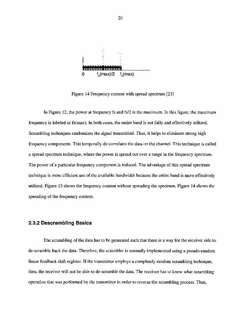
Figure 14 Frequency content with spread spectrum [23]
In Figure 12, the power at frequency fs and fs/2 is the maximum. In this figure, the maximum
frequency is labeled as fs(max). In both cases, the entire band is not fully and effectively utilized.
Scrambling techniques randomizes the signal transmitted. Thus, it helps to eliminate strong high
frequency components. This temporally de-correlates the data on the channel. This technique is called
a spread spectrum technique, where the power is spread out over a range in the frequency spectrum.
The power of a particular frequency component is reduced. The advantage of this spread spectrum
technique is more efficient use of the available bandwidth because the entire band is more effectively
utilized. Figure 13 shows the frequency content without spreading the spectrum. Figure 14 shows the
spreading of the frequency content.
2.3.2 Descrambling Basics
The scrambling of the data has to be generated such that there is a way for the receiver side to
de-scramble back the data. Therefore, the scrambler is normally implemented using a pseudo-random
linear feedback shift register. If the transmitter employs a completely random scrambling technique,
then, the receiver will not be able to de-scramble the data. The receiver has to know what scrambling
operation that was performed by the transmitter in order to reverse the scrambling process. Thus,
21
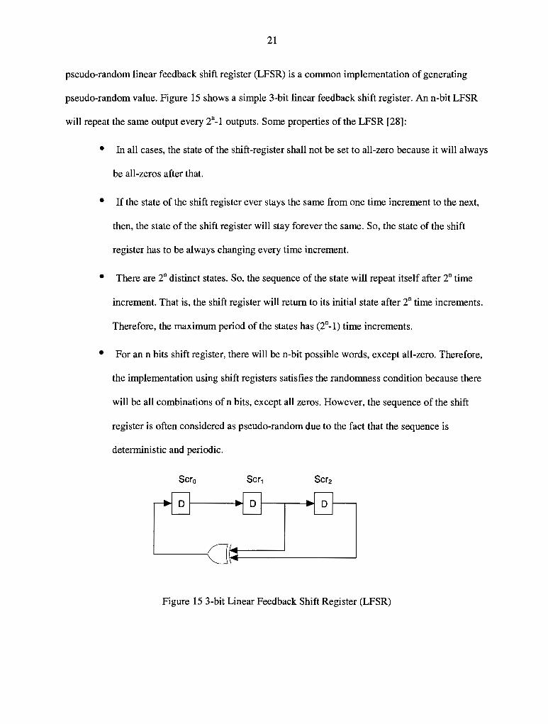
pseudo-random linear feedback shift register (LFSR) is a common implementation of generating
pseudo-random value. Figure 15 shows a simple 3-bit linear feedback shift register. An n-bit LFSR
will repeat the same output every 2n-l outputs. Some properties of the LFSR [28]:
• In all cases, the state of the shift-register shall not be set to all-zero because it will always
be all-zeros after that.
• If the state of the shift register ever stays the same from one time increment to the next,
then, the state of the shift register will stay forever the same. So, the state of the shift
register has to be always changing every time increment.
• There are 2n distinct states. So, the sequence of the state will repeat itself after 2n time
increment. That is, the shift register will return to its initial state after 2n time increments.
Therefore, the maximum period of the states has (2n-1) time increments.
• For an n bits shift register, there will be n-bit possible words, except all-zero. Therefore,
the implementation using shift registers satisfies the randomness condition because there
will be all combinations of n bits, except all zeros. However, the sequence of the shift
register is often considered as pseudo-random due to the fact that the sequence is
deterministic and periodic.
Scro Scr1
Figure 15 3-bit Linear Feedback Shift Register (LFSR)

22
2.3.3 Convolutional Codes
The code-groups generated using Linear Feedback Shift Register are convolutional codes.
Convolutional codes are special types of block codes. The reasons for using block codes are [23]:
• rich transition densities. Thus, it provides easier clock recovery.
• DC balanced codes to be used.
• non-data codes, which are control codes. For lO00BASE-T, control codes are IDLE, Start
of Stream Delimiter (SSD), End of Stream Delimiter (ESD), etc .. .
Some block codes that are used by Ethernet are 4B/5B, 8b/10b, 6B/3T, etc ... For example,
lO0BASE-TX employs 4B/5B coding scheme.
Convolutional codes can be implemented by using the convolution of the input sequence with
the generator sequence. One example of generator sequence is the sequence of the linear feedback
shift register. That is using XOR gate to generate the effect of convolution of the input sequence and
the generator sequence. In short, convolutional codes are just the other way of saying Linear
Feedback Shift Register (LFSR).
2.4 1000BASE-T Coding System
2.4.1 Selecting the Channel Symbols
The lO00BASE-T PHY will interface to the upper layers via the 8 bit TXD<7:0> through the
GMII. Therefore, every 8ns, which is the clock period, the PHY will receive or send out an 8-bit
word. So, the encoding choice is to encode the 8-bit word into some symbol space. To achieve the
rate of 1000 Mbps, all four wire-pairs have to transmit at 250Mbps per wire-pair. Since there are eight
bits of data to be transmitted at every transmit clock, it creates a total of 28 possible combinations of
23
the bits. Therefore, 28 = 256 symbols are needed to represent the 8-bit data. To represent 256 different
symbols, we can use 4 levels of signal on each wire-pair. This will give 44 = 256 different
combinations. However, 4 levels of signal on each wire-pair will only produce enough combinations
for data code-group. 256 combinations are not sufficient considering that it will be necessary to have
additional symbols for denoting control code-groups and idle code-groups. As a result, we need to
have 5 levels on each wire-pair in order to have enough symbols. Five levels will have 54 = 625
symbols, which will be adequate for symbolizing the data code-groups and other control code-groups.
The Physical Medium Attachment (PMA) will process these 5 levels of symbols to the
corresponding voltages before sending out to the wire-pairs. The 5 levels of signal to be sent on the
four wire-pairs are+/- 1 V, +/- 0.5 V. +/- IV are mapped to symbols+/- 2, +/- 0.5 V are mapped to
symbols+/- 1, and 0 Vis mapped to symbol 0.
2.4.2 Defining the 4D/PAM5 Structure
Pulse Amplitude Modulation (PAM) combined with trellis coding and Viterbi decoding is the
basic transmission scheme used in the 802.3ab standard. The scheme uses a 5-level { -2, -1, 0, 1, 2}
PAM signal on 4 wire-pairs. Therefore, it is considered 4D/PAM5 (four-dimensional and 5-level
Pulse Amplitude Modulation)[23]. To explore more about 4D/PAM5, this section first discusses the
separation of the odd and even subsets. These subsets are the basic structure that composes the Trellis
structure that will be discussed in the following section (2.4.3 Trellis Structure).
The symbols are divided into two subsets, X and Y. The symbol subsets are defined as: X =
{ -1, + 1}, Y = { -2, 0, + 2}. In 1 000BASE-T, there are four wire-pairs. Hence, as each of the four
channels can send a symbol from subsets X or Y, there are naturally 16 combinations of the possible
symbols pairs. Out of the 16 combinations, 8 combinations are chosen as the symbol subsets. Table 2

24
shows the symbol subsets used in lOOOBASE-T. For a complete symbol-mapping table, refer to
APPENDIX A.
The even subsets in Table 2 are DO, D2, D4 and D6. The odd subsets are Dl, D3, D5, and
D7. The intermediate bit in the generation of code-groups, Sdn[6:8], are the subset index for the
symbol mapping. These three bits are the encoded bits from the trellis encoder. Refer to Figure 16 for
the generation of these three bits. For example, the subset DO is chosen when the bits Sdn[6:8] is 000.
When DO is chosen, the final code-groups generated will be in the form of XXXX or YYYY. The
total number of elements that is possible through the odd subsets and even is indicated in Table 2. All
these odd and even subsets are the basic structure for the trellis diagram. Trellis structure of
lOOOBASE-T is explained in the following section: 2.4.3 Trellis Structure.
Table 2 Subset mapping
Subsets Sdn[6:8] Pattern 1 Number of Pattern 2 Number of Total TA, TB, TC, TD Elements in TA, TB, TC, Elements in Number
1 TD 2 of Elements
DO 000 xxxx 16 yyyy 81 97 D2 010 XXYY 36 YYXX 36 72 D4 100 XYYX 36 YXXY 36 72 D6 110 XYXY 36 YXYX 36 72 Dl 001 XXXY 24 YYYX 54 78 D3 011 XXYX 24 YYXY 54 78 D5 101 XYYY 54 YXXX 24 78 D7 111 XYXX 54 YXYY 54 78
2.4.3 Trellis Structure
1 OOOBASE-T employs the trellis structure shown in Figure 17. The trellis diagram is
separated into two sub-trellis: even sub-trellis and odd sub-trellis. The utilization of trellis structure is
because it allows error correction using Viterbi decoder. The error correction Viterbi decoder resides
in the Physical Medium Attachment (PMA).

25
Table 2 shows that when the bits of Sdn[6:8], the intermediate bits in the process of
generating code-groups, are 000, the subset DO shall be used. Figure 16 shows the trellis encoder used
in the PCS Transmit function. The trellis encoder encodes eight data bits into the nine mapping bits,
Sdn[8:0]. The three bits Sdn[6:8} act as the subset index to the trellis diagram in Figure 17. The
remaining bits, Sdn[5:0], are used to select the points within the subsets. This means that when the
bits csn[0:2] are 000 and the bits Sdn[6:8] are 010, the transition is from state "A" to state "B" in
Figure 17. Following the transition, the encoder bits will become 001. When the encoder bits are 000,
the permissible paths are DO, D2, D4, and D6. Similarly, when the encoder bits are 001, the
permissible paths are DI, D3, D5, and D7. Only valid transitions through the trellis structure will be
transmitted. Therefore, the separation of even and odd subsets limits the valid paths in the Trellis
diagram. Hence, this structure of the path aids the error correction of Viterbi decoding. Viterbi
decoder will utilize the same structure as the trellis structure. Therefore, with the knowledge of the
valid transitions of the symbols, the errors can be corrected using Viterbi decoder. Since the Viterbi
decoder is not in the Physical Coding Sublayer, the details about Viterbi decoder won't be discussed
in this work. Refer to [6] and [29] for further information on Viterbi algorithm.
Scrambler --..i (Bitwise XOR)
Figure 16 Trellis Encoder
coding:_enable
Sd0 [0] Sd.[J]
d,.[2] .sd,,[3)
[4] .,,sd.,[5]
n[6] [7]
~[8)
Points in Subset
Subset Index
DI D3 D5 D7
D2DOD6D4
D3 D1 D7D5
D4D6D0D2
D5D7Dl D3
cs [0:2)
Conv~lutional Encoder Bits at time n
001
010
011
100
IOI
D6D4D2 DO 110
D7D5 D3 Dl 111
26
CSn+l[0:2) Convolutional Encoder Bits at time n+ I
OD2D4D6
~7"' -~-;.-=rn,tlfil D2 DO D6 D4
D4 D6DOD2
D6D4D2DO
D1 D3 D5D7
D3 DI D7D5
D5 D7D1 D3
D7D5D3Dl
Figure 17 Trellis Diagram
2.4.4 The Master/Slave Scramblers employed
Scrambling is used to randomize the sequence of transmitted symbols and avoid the presence
of spectral lines in the transmitted signal spectrum. Scrambling also creates essentially uncorrelated
data symbols, which improves operation of the adaptive receiver functions. Many of the principles
and techniques proposed for the lOOOBASE-T design approach have already been employed in three
lOOBASE-T (Fast Ethernet) copper physical layer solutions:
• 1 OOBASE-TX, which runs on 2 pairs of Category 5 cabling with a 125Mbaud symbol rate
and binary encoding,
• 100BASE-T4, which runs on 4 pairs of Category 3 or better cabling with a 25Mbaud
symbol rate and ternary encoding, and

27
• 100BASE-T2, which runs on 2 pairs of Category 3 or better cabling with a 25Mbaud
symbol rate with quinary encoding and DSP processing to handle the potential problems of
alien signals in adjacent wire-pairs (alien crosstalk)
l00BASE-TX demonstrates that it is possible to send a symbol stream over Category 5 cable
at 125Mbaud. 100BASE-T4 demonstrates techniques for sending multi-level coded symbols over
four pairs. 100BASE-T2 utilizes digital signal processing (DSP), five-level coding, and simultaneous
two-way data streams while dealing with alien signals in adjacent pairs. The scrambler used for
lOOOBASE-T is a 33 bits Linear Feedback Shift Register. That's 233 - 1 or 8589934591 time
increments before the LFSR pattern repeats. The scrambler for lOOBase-TX has only 211-1 or 2047
different sequence before it repeats.
master .. ... ..
0 2 12 13 19 20 32 33
~---~---~---~T slave~ 12 13 20
'---------(]{14-=-------~
Figure 18 Side-stream scrambler for Master and Slave [16]
The two parties on a l000BASE-T link are referred to as Master and Slave. The Master is the
clock source. The Slave recovers the Master's clock and uses that clock to transmit and receive. The
process of how the determination of which station will be the Master or the Slave is developed in
PHY Control and Auto-Negotiation. The PMA PHY Control function indication whether the PHY
shall behave as a Master or a Slave via the PMA_CONFlG.indicate message. When the parameter
con.fig is set, the PHY shall act as a Master, when the parameter config is cleared, the PHY shall act as
a Slave. Figure 18 shows the side-stream scrambler for Master and Slave. For Master, the PCS

28
Transmit shall use the Master side-stream Scrambler. For Slave, the PCS Transmit shall use the Slave
Side Stream Scrambler.
2.5 Physical Coding Sublayer (PCS) Functions
The Physical Coding Sublayer (PCS) consists of 4 functions: PCS Transmit, PCS Data
Transmission Enable, PCS Carrier Sense and PCS Receive. Figure 19 shows these four operating
functions for the PCS and the interfaces to the Gigabit Media Independent Interface (GMII) and the
Physical Medium Attachment (PMA). The reset signal pcs_reset from the PMA to the PCS will
initialize all these four functions. The parameter pcs_reset will be set whenever the power on or the
receipt of a request for reset from the management entity.
GTX_CLK
TXD<7:0>
COL
TX_EN
TX_ER
TX_EN
RX_CLK RXD<7:0> RX_DV RX_ER
... ....
... -.... ... ... ....
PMA_UNITDATA.request(tx_symb_ vector) ... ... ... tx_IIK>de ... PCS .... ... ...
Transmit ... ... .... .... -... .... ... .... TX_EN .. .. ...
tx_errorT ,tx_enable
... PCS Data link_status ... ...
Transmissio .... ... ... nEnable
1uw0Ttransmit ...
PCS Carrier ... I""
Sense -....
1 OOOBTreceive ... config
PCS I ... - loc_rcvr_status Receive : PMA UNITDATA.indicate(rx svmb vector)
scr_status ... rem_rcvr_status ... ...
Figure 19 PCS functions [16]
29
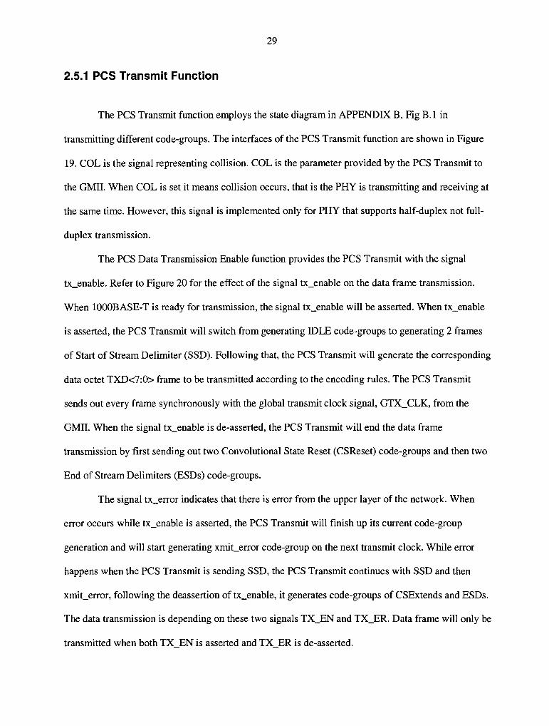
2.5.1 PCS Transmit Function
The PCS Transmit function employs the state diagram in APPENDIX B, Fig B. l in
transmitting different code-groups. The interfaces of the PCS Transmit function are shown in Figure
19. COL is the signal representing collision. COL is the parameter provided by the PCS Transmit to
the GMII. When COL is set it means collision occurs, that is the PHY is transmitting and receiving at
the same time. However, this signal is implemented only for PHY that supports half-duplex not full-
duplex transmission.
The PCS Data Transmission Enable function provides the PCS Transmit with the signal
tx_enable. Refer to Figure 20 for the effect of the signal tx_enable on the data frame transmission.
When lO00BASE-T is ready for transmission, the signal tx_enable will be asserted. When tx_enable
is asserted, the PCS Transmit will switch from generating IDLE code-groups to generating 2 frames
of Start of Stream Delimiter (SSD). Following that, the PCS Transmit will generate the corresponding
data octet TXD<7:0> frame to be transmitted according to the encoding rules. The PCS Transmit
sends out every frame synchronously with the global transmit clock signal, GTX_CLK, from the
GMII. When the signal tx_enable is de-asserted, the PCS Transmit will end the data frame
transmission by first sending out two Convolutional State Reset (CSReset) code-groups and then two
End of Stream Delimiters (ESDs) code-groups.
The signal tx_error indicates that there is error from the upper layer of the network. When
error occurs while tx_enable is asserted, the PCS Transmit will finish up its current code-group
generation and will start generating xmit_error code-group on the next transmit clock. While error
happens when the PCS Transmit is sending SSD, the PCS Transmit continues with SSD and then
xmit_error, following the deassertion of tx_enable, it generates code-groups of CSExtends and ESDs.
The data transmission is depending on these two signals TX_EN and TX_ER. Data frame will only be
transmitted when both TX_EN is asserted and TX_ER is de-asserted.
30
The PCS Transmit generates code-groups (An, Bn, Cn, Dn) to be passed to the PMA to be
sent out on wire-pairs BI_DA, BI_DB, BI_DC, and BI_DD. An, Bn, Cn, and Dn are the symbols that
are represented as 3-bit parameters. The PCS Transmit generates code-groups at the rate of 8ns.
There are three different modes of operations: normal, idle and zero. The parameter tx_mode controls
these three modes of the operation of the PCS Transmit. SEND _N for normal operation, SEND _I for
idle operation, SEND_Z for zero operation.
tx_enablen
TXD[7:0) x Data stream x SSDn
csreset0
ESDn
An ... Dn
IDLE Data SSD csreset ESD IDLE
Figure 20 Transmission frame structure [16]
During the normal mode of operation, indicated by tx_mode equals to SEND _N, the PCS
Transmit generate the code-group sequences according to the frame structure depicted by Figure 20.
If the parameter tx_mode indicates SEND _I, the PCS Transmit generates sequences of idle code-
groups. During the idle transmission, the symbols used are { +2, 0, -2}. If the parameter tx_mode
indicates SEND_Z, the PCS Transmit passes a vector of zeros at each 8ns to the PMA.
The PCS Transmit uses linear feedback shift register to generate the sequences of Scm[0:33].
Figure 18 shows the master and slave scrambler. The sequences of Scm[0:33] are then used to
generate Sxn and Sgn. Figure 21 shows the process of creating Sxn and Sgn. They are some XOR
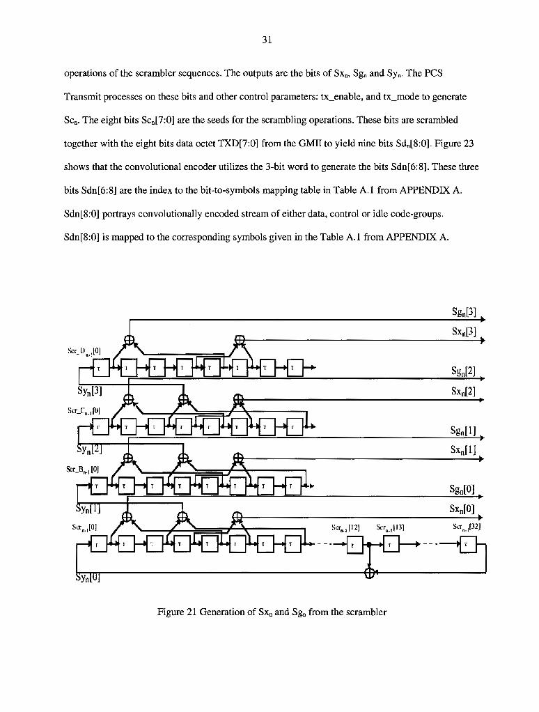
31
operations of the scrambler sequences. Ti:ie outputs are the bits of Sxn,--Sgn am.l Syn. The PCS
Transmit processes on these bits and other control parameters: tx_enable, and tx_mode to generate
Sen. The eight bits Scn[7:0] are the seeds for the scrambling operations. These bits are scrambled
together with the eight bits data octet TXD[7:0] from the GMII to yield nine bits Sdn[8:0]. Figure 23
shows that the convolutional encoder utilizes the 3-bit word to generate the bits Sdn[6:8]. These three
bits Sdn[6:8] are the index to the bit-to-symbols mapping table in Table A. I from APPENDIX A.
Sdn[8:0] portrays convolutionally encoded stream of either data, control or idle code-groups.
Sdn[8:0] is mapped to the corresponding symbols given in the Table A. I from APPENDIX A.
Scr11• 1 I 12] Scr,)32]
Figure 21 Generation of Sxn and Sgn from the scrambler

32
tx_enable,,
Sx,,[3:0] TD,, D,,
Sc,.[7:0] Scrambling & Sd,,[8:0] TC,, c,, IFSR XOR Qld/ Symbol Scrn[32:0] Equatirns Even Convolutirnal Mapping B,,
Oxling Fnco:ling T A.,
tx_enable,,
SnA,,
SnB,,
Syn[3:0] Sign
SnC,, Fnco:ling SnD,,
Figure 22 Processes of generating code-group An, Bn, Cn and Dn
Tx_D 0 [0:7]
..Sd0 [0] Sd.[l] Points
Sc11[0:7] d.(2] in Scrambler d,,[3] Subset (Bitwise XOR) Sd,,[4]
1>Sd,,[5] .[6]
Subset
Sd,,[8] Index
coding:_enable
Figure 23 Scrambling and convolutional encoding

33
2.5.2 PCS Data Transmission Enable Function
The PCS Data Transmission Enable function processes TX_EN, TX_ER, tx_mode and
generates the signals tx_enable and tx_error. It enables or disables the transmission of data through
these two signals. The operation of the PCS Data Transmission Enable is depicted in Fig B.5 of
APPENDIXB.
2.5.3 PCS Carrier Sense Function
CRS is the Carrier Sense signal for allocating a multiple-accessed channel. When Carrier
Sense is ON, the PCS will indicate to the GMII by asserting CRS. This allows the station with data to
transmit to first listen to determine if another station is sending data. When the carrier sense is OFF,
the PCS will indicate to the GMII by de-asserting CRS. Fig B.4 in APPENDIX B shows the state
diagram for the PCS Carrier Sense function.
2.5.4 PCS Receive Function
Fig B.2 and Fig B.3 in APPENDIX B show the state diagram for the PCS Receive function.
The PCS Receive obtains received data from the PMA via tx_symb_ vector. This parameter is
implemented as 4 3-bit parameters.
The PCS Receive will process the received signals and pass to the GMII with RX_CLK
(received clock), RXD<7:0> (received data), RX_DV and RX_ER. RX_DV is asserted when receive
is enabled and RX_ER is asserted when there is error in received sequence. The PCS Receive uses the
knowledge of the PCS Transmit encoding rules that are used during the idle mode to execute proper
decoding. The vectors (An, Bn, Cn, Dn), as parameter tx_symb_vector, are received from the PMA.

34
The PCS Receive will decode these symbols and produce the data RXD[7:0] and pass it to the GMII.
The parameters RX_DV and RX_ER are determined are shown in the state diagram of the receive
function in Fig B.2 and Fig B.3 in APPENDIX B.
The parameter loc_rcvr_status conveys the information about the correct receiving operation
by the PMA. When loc_rcvr_status indicates OK, the PCS Receive will continuously check on the
received sequences that satisfy the encoding rules used in the idle mode. When the code-group of
SSD is detected, the parameter lO00BaseTreceive will be sent out to the PCS Carrier Sense and the
PCS Transmit. This parameter will further assist these two functions to detect the collision, which is
when the PCS is receiving and transmitting at the same time. This parameter is implemented for the
lO00BASE-T PHY which support half-duplex instead of full-duplex operation.
According to the rules as described by the receive state diagram in Fig B.2 and Fig B.3 in
APPENDIX B, the RX_ER is also processed by the PCS Receive function. During the arrival of the
data stream, the PCS Receive continuously decode the data following the encoding rules of the data.
Detection of the code-groups ESDs reveal the end of the reception of data, the PCS Receive will de-
assert the parameter RX_DV on the GMII.
The PCS Receive shall de-scramble the data stream and produce the proper sequence to
generate RXD[7:0] to the GMII. For Master PHY, the side-stream scrambler shall employ the de-
scrambler generator polynomial of gM(x) = 1 + x20 + x33, and for the Slave PHY, the side-stream
scrambler shall employ the de-scrambler generator polynomial of gs(x) = 1 + x13 + x33•
The PCS Receive obtains the symbols from the PMA as (An, Bn, Cn, Dn)- These symbols are
XOR with the sign of the symbols: SnAn, SnBn, SnCn and SnDn to get TAn, TBn, TCn and TDn. The
symbols are reverse mapping to get the values Sdn[7:0]. Sdn[7:0] are further processed to obtain
RXD[7:0]. RXD[7:0] is the data that will be sent to the upper layer of the network through the GMII.

LFSR Scru[32:0]
XOR Equations
2.6 Conclusion
Sign Decoding
Srev
35
SnC,,
SnDu
Reverse Mapping
Sxn[3:0] Reverse Convolution t---• &Decoding
Figure 24 Receive Function: Decoding of RXD[7:0]
In this chapter, the IEEE standard 802.3ab (lO00BASE-T) was described. The top-level
1 000BASE-T system and the PCS' s main function were highlighted. The interface of the Physical
Coding Sublayer (PCS) with the Gigabit Media Independent Interface (GMII) and the Physical
Medium Attachment (PMA) was shown. In the next chapter, the simulations results for the PCS layer
will be shown.
36
3 PCS TESTING AND SIMULATION RESULTS
3.1 Introduction
In this chapter, the results from the simulations and testing for Physical Coding Sublayer are
discussed. The implementation and simulations of the PCS were written in Verilog Hardware
Descriptive Language. In the first section, the top level of the PCS layer is introduced. The whole
PCS design was implemented by dividing it into several smaller sub-modules. The first section will
show the composition of all the PCS modules. In section 3.3, the simulation results of the PCS
Transmit function are shown. The following sections show the simulations results for the PCS Data
Transmission Enable function, the PCS Carrier Sense function and PCS Receive function
respectively. Then, the simulations results for all the intermediate parameters will be shown.
3.2 PCS Top Level
Figure 25 shows the hierarchy of the PCS. The PCS contains four main modules: PCS
Transmit, PCS Data Transmission Enable, PCS Carrier Sense and PCS Receive. The sub-modules are
the Transmit State Machine, PCS scrambler, PCS GenerateSymbols and Transmit RAM. Transmit
State Machine sub-module is the function that controls the state of the Transmit function. The
corresponding state diagram for this state machine is in APPENDIX B. The PCS scrambler sub-
module does the scrambling of the data. It generates the scrambler seeds that are needed to generate
the code-groups. The PCS GenerateSymbols takes in the output of the scrambler and produces the
corresponding code-groups. It contains the Transmit RAM (Random Access Memory). This RAM is
the implementation of the bit-to-symbol mapping tables shown in APPENDIX A. The PCS

37
GenerateSymbols will generate the symbols with the bit-to-symbol mapping information stored in the
Transmit RAM.
The PCS Receive module consists of several sub-modules: PCS Descrambler, PCS Symbol
Sign and Receive State Machine. The PCS Descrambler contains the same Linear Feedback Shift
Register as the PCS Scrambler. This is to generate the same scrambler seeds for the scrambling
operation. The PCS Symbol Sign will take in the output generate by the PCS Descrambler and decode
the sign of the symbols being received. With the decoded signs, the PCS State Machine will decode
the code-groups. The decoding of code-groups the reverse of the bit-to-symbol mapping. Thus, the
decoding operation is actually symbol-to-bit mapping. Symbol-to-bit information is stored in the
Receive RAM.
PCS
I I I I
PCS PCS Data PCS Carrier PCS Transmit Transmission Sense Receive
Enable I I
I I I I I I TxState PCS PCS PCS PCS Rx State Machine Scrarrhler Generate Ixscrarrhle Syrrbol Sign Machine
Syrrbols I
I I I Receive ll!coding Transmit RAM
RAM
Figure 25 Hierarchy of the top level PCS

38
Figure 26 shows the simulation results for the PCS top level. GTX_CLK is the global
transmit clock that runs at periods of 8ns. At the beginning, pcs_reset resets the functions of
transmitter and receiver. The transmitter and receiver are IDLE for a few clock period. At the
assertion of the TX_EN (transmit enable signal), the PCS Transmit sends out two bytes of SSD
before sending out the data frames corresponding to the data octet TXD[7:0]. On the receiver side,
after two bytes of SSD were received, the receiver received the data frames. On the figure, it can be
seen that, the data, RXD of '02', '04', '08', etc, were received. Then, at the de-assertion of TX_EN, the
receiver receives the frames of CSReset and then ESD sent out by the transmitter. RX_DV (receive
enable) and RX_ER(receive error) are the received signals for TX_EN and TX_ER.
;::. ~~---------+------+------+-----+--+--~ -
I TX_E~
I
' ' r"' r"' f, -2-0~[+-t-o ~i--------+---+----+--8-0 ---,,----+--
:-'--!----+---"-+--' aa
RX_ xi DV .... ____ ___,
i-~
RX_ ER ' ' ~"'-----------------~------------------RXD (7:0]
IDLE sso
' 02: D4 DB: 10 20: 40 8D CSResef, ESD IDLE
' ' ' ' '
Figure 26 Simulation results for PCS top level

39
3.3 PCS Transmit
The interfaces of the input and output signals for the PCS Transmit can be seen in Figure 19.
Figure 27 shows the simulation results for the PCS Transmit function. The PCS transmit sends the
SSD and follow by the data frame when the signal tx_enable is asserted. On the receiver side, it
shows that the '55' is received. '55' stands for the SSD. Then, the data transmitted out are '02', '04',
'08', etc. As the tx_enable goes to zero, the PCS transmit sends out CSReset and ESD. This is verified
when the receiver's decoded data is '55', which represents the code-groups of CS Reset and ESD.
Then, the PCS transmit goes IDLE. At this time, the receiver receives '00', which represent IDLE.
Figure 27 S mulation resu ts for PCS Transmit function

40
The link_status denotes the 1 000BASE-T link. When the link_status is one, it indicates that a
valid lO00BASE-T link is established. So, when the link_status is zero, it disables the PCS
transmission by de-asserting the tx_enable signal. The parameters baseTtransmit and baseTreceive
are the variables lO00baseTtransmit and lO00baseTreceive. These two parameters are used to
determine the value of COL. COL, representation of the existence of collision, is implemented only
for half-duplex.
3.4 PCS Data Transmission Enable
Ref er to Figure 19 for the signal interfaces for the PCS Data Transmission Enable function.
Figure 28 shows the simulation results for the PCS Data Transmission Enable function. This function
generates the output signals tx_enable and tx_error. These two output signals depend on the input
signals of pcs_reset, link_status, tx_mode, TX_EN and TX_ER. When reset happens, both tx_enable
and tx_error go low. The link_status denotes the l000BASE-T link. When the link_status is one, it
indicates that a valid lO00BASE-T link is established. When the link_status is zero, it disables the
transmission by de-assert the tx_enable signal. The parameter tx_mode controls these three modes of
the operation of the PCS Transmit: SEND_N (1) for normal operation, SEND_! (2) for idle operation,
and SEND_Z (0) for zero operation.
During the normal mode of operation, indicated by tx_mode equals to SEND_N, the PCS
Transmit generates the data code-group sequences according to the frame structure depicted by Figure
20. However, if the parameter tx_mode indicates SEND_!, the PCS Transmit generates sequences of
idle code-groups. During the idle transmission, the symbols used are from the set of { +2, 0, -2}. If the
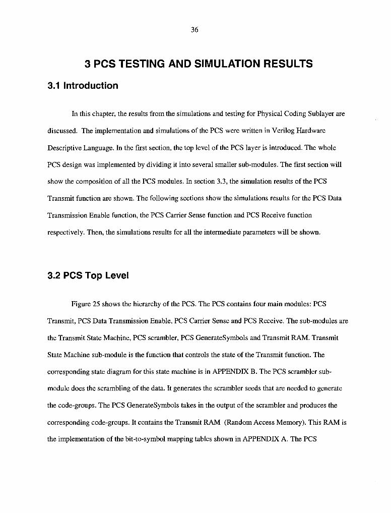
parameter tx_mode indicates SEND _Z, the PCS Transmit passes a vector of zeros at each 8ns to the
PMA.

41
When the link_status is valid, the tx_mode is one, and there is no reset, then, the output signal
tx_enable is assigned to TX_EN and the tx_error is assigned to TX_ER. These two signals, TX_EN
and TX_ER, are from the GMII. The outputs, tx_enable and tx_error, will be passed to the PCS
Transmit for controlling the transmission operation. Refer to Fig B.5 in APPENDIX B for the state
machine of the PCS Data Transmission Enable function.
::et~ link ~! ===:::::;-, ~!,. --------;:::=i========l=i,' =====l=====~:=====l===== stafusj _ :· b;~ ------==!==I =-+-------i-------~ I l LJ ~-
~nableLJ7-+--------+---~ ! ~I--+----+-----+-------~rror ,,,__i -----------~ILJl ______________ _
Figure 28 Simulation results for PCS Data Transmission Enable function
3.5 PCS Carrier Sense
The main function of carrier sense is the generation of the signal CRS, which is to be sent to
the GMII. The CRS is the signal representing the carrier sense of the physical layer. CRS is driven by
the PHY. This function is implemented for the PHY that supports only half-duplex transmission. The
CRS will be asserted when either the transmit or the receive medium is non-idle and will be de-
asserted when both the transmit and receive media are idle. Figure 29 shows the simulation results for
the PCS Carrier Sense function. Fig B.4 in APPENDIX B shows the state machine of the PCS Carrier
Sense function.
pcs_ reset
link_ status
repeat er mode
baseT transmit
baseT receive
42
~'-------+-------....----
LJ
CRS rulJ I II._____________._
Figure 29 Simulation results for PCS Carrier Sense function
3.6 PCS Receive
The function of the PCS Receive is to decode the code-group received from the PMA and
send it as an octet data, RXD[7:0], to the GMII. The method used in the decoding of the code-groups
received were discussed in section 2.5.4 PCS Receive Function.
To begin the data transmission, the PCS transmit sends two bytes of Start of Stream Delimiter
(SSD) and follow by the data frames when the signal tx_enable is asserted. After two frames SSD, on
the receiver side, it shows that the '55' is received. '55' stands for the SSD. Then, the data transmitted
out are '02', '04', '08', etc. As the tx_enable goes to zero, the PCS transmit sends out CSReset and
ESD. Both the CSReset and the ESD frames are represented using the symbols '55'. This is verified

43
when the receiver's decoded data is '55', which represents the code-groups of CSReset and ESD.
Then, the PCS transmit goes IDLE. At this time, the receiver receives '00', which represent IDLE.
The PCS Receive produces the signals RX_ER (receive error) and RX_DV (receive enable) to the
GMII. RX_ER is set when there is an error exists in receiving data. RX_DV represents the receive
enable. The parameter baseTreceive is to indicate the PCS Transmit that the lO00BASE-T receiver is
receiving data. The parameter baseTtransmit is to indicate the PCS Receive that the lO00BASE-T
transmitter is transmitting data. This signal is used to generate the parameter COL (collision).
Collision occurs when both the baseTtransmit and baseTreceive are set.
RXD ! (7:0] j
I r-- - ·-
I -· I I I ·- ,--' - - .,_
2 0 08 10 20 10
__ : - - :_ .,..;.. ....... : I_
:_ ,...;.. -·
80
55 po ' ;~----r---"--i-~--r--.....,,...~--;---;------;;----+--+---;------;r---+--+--+-"----i---+--+--'
Figure 30 Simulation results for PCS Receive function
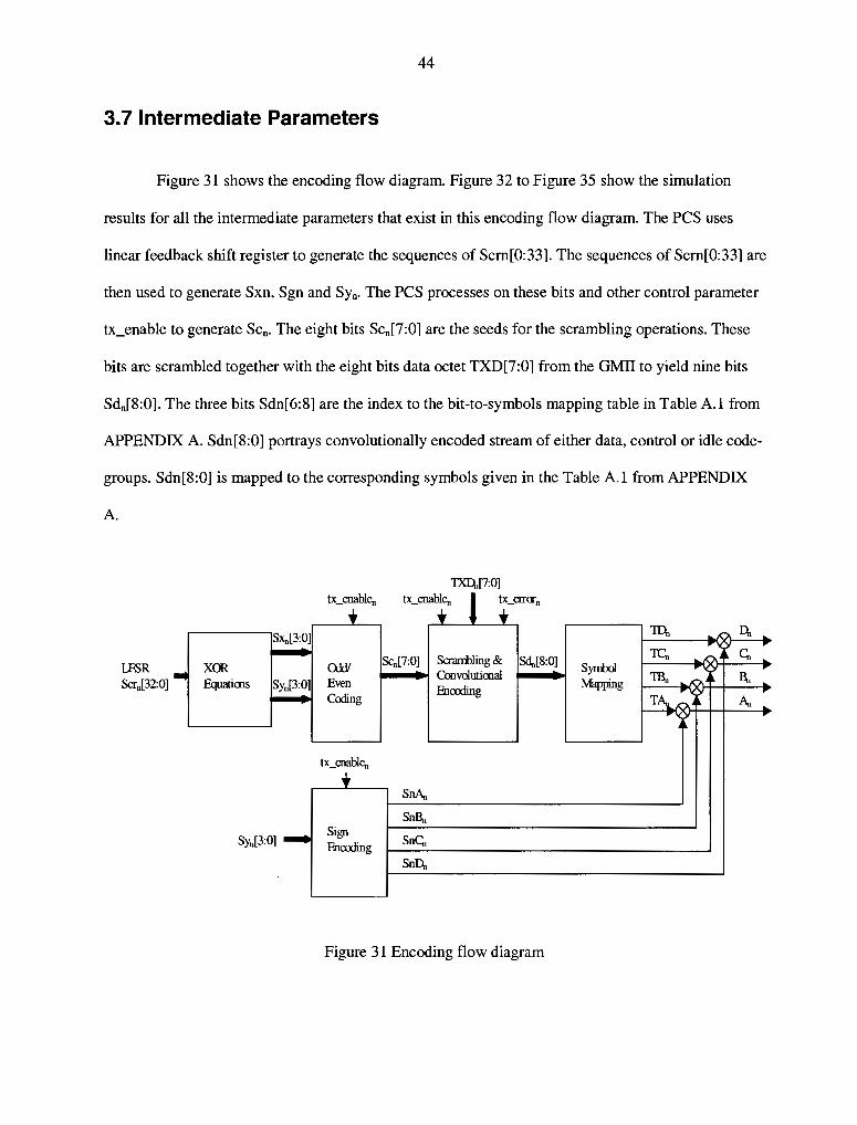
44
3.7 Intermediate Parameters
Figure 31 shows the encoding flow diagram. Figure 32 to Figure 35 show the simulation
results for all the intermediate parameters that exist in this encoding flow diagram. The PCS uses
linear feedback shift register to generate the sequences of Scm[0:33]. The sequences of Scm[0:33] are
then used to generate Sxn, Sgn and Syn, The PCS processes on these bits and other control parameter
tx_enable to generate Sen, The eight bits Scn[7:0] are the seeds for the scrambling operations. These
bits are scrambled together with the eight bits data octet TXD[7:0] from the GMII to yield nine bits
Sdn[8:0]. The three bits Sdn[6:8] are the index to the bit-to-symbols mapping table in Table A.1 from
APPENDIX A. Sdn[8:0] portrays convolutionally encoded stream of either data, control or idle code-
groups. Sdn[8:0] is mapped to the corresponding symbols given in the Table A.1 from APPENDIX
A.
tx_enable,,
Sx,.[3:0] ID,,
Sc,.[7:0] Scrani>ling& Sd,.[8:0] 'IC,, IFSR XOR Oil/ Symbol ScrJ32:0] Equatims Even Coovolutiooal .Mapping
Coding Fnooding T
tx_enable,,
SnA.,
SnB.,
Syn[3:0] Sign
SnC,. Fnooding SnD,,
Figure 31 Encoding flow diagram

GTIC_ CLK
Scm
r .~,, 1 !01010!0 1e1eie1e0
45
·~
1c3c3c3c 1 87878783 101010!07 e1 e1 e 01
Figure 32 Simulation results for parameters: Scr0 , Sg0 , Sxn and Sy0
GTIC CLK
~--'
Sen :X X 02 Od 07 2g 03 3d 13 4d 03 Od 81 01: 45 6a 65 4b ct go c8 d6 •• 55 33
' '
03c3c3c11
' 8d ~d 52
Figure 33 Simulation results for parameters: Sc0 , SnAn, SnBn, SnCn and SnDn
-
dt
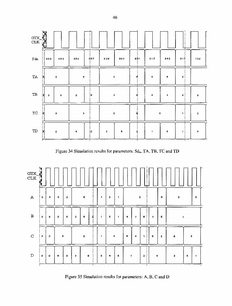
46
GTX
CLK ~-· ~~--.,----:..._-----~----v--------------.:.-..,.....-____,.
' ' ' Sein : 000 002 00d d07 029 003 O~f 017 045 01j 12d
'
Figure 34 Simulation results for parameters: Sdn, TA, TB, TC and TD
Figure 35 Simulation results for parameters: A, B, C and D

47
3.8 Conclusion
The results from the simulations and testing for the physical Coding Sublayer were discussed.
The implementation and simulations of the PCS were written in Verilog Hardware Descriptive
Language. The results of the top-level PCS simulations were presented. Followed by the simulation
results for the PCS's four main functions: the PCS Transmit, the PCS Data Transmission Enable, the
PCS Carrier Sense, and the PCS Receive. Then, the simulations results for all the parameters in
encoding flow diagram were shown.
48
4 SYNTHESIS AND SIMULATION RESULTS
4.1 Introduction
In the previous chapter, the Verilog HDL simulation results for the Physical Coding Sublayer
(PCS) were shown. In this chapter, synthesis concepts are introduced. Then, the results from synthesis
are discussed. The PCS was synthesized using Synopsys® with two process libraries: 0.35µm CMOS
and l.4µm CMOS. Two synthesis techniques: hierarchical optimization and hierarchical-flattening
optimization, were chosen to compare the area and timing tradeoffs between them. The automation of
the synthesis was accomplished with the creation of synthesis script files. With these script files, the
PCS can be synthesized automatically with any target library desired. Finally, the gate-level
simulation results are shown.
4.2 Synthesis Overview
In this section, synthesis concepts are introduced. Synthesis steps are explained. Then, the
synthesis techniques that were used in this research are described. The results of the synthesis work
will be discussed in the following section.
Synthesis generates the netlists from the Verilog HDL descriptions. Synthesis can be divided
into three major steps: translation, optimization and mapping. Figure 36 shows the three major steps
carried out by a synthesis tool, Synopsys Design Compiler. Translation involves the conversion from
HDL descriptions to gate-level netlists. The gate-level netlists is the generic boolean representation of
the gates. Generic boolean representation means that the gate-level netlist is general and technology
independent. It is also called the generic technology (GTECH). The technology library is the file that
describes all the characteristics of the leaf-cells defined.

49
For this thesis, two different process libraries were used: 0.35µm CMOS and l.4µm CMOS.
When the optimization is carried out, the synthesis tools will optimize the circuits under the control of
the designers. The designers can set the timing, area and power constraints that are desired. Logic
synthesis tools infer gates to meet these constraints. Logic optimization performs a series of factoring,
substitution and elimination steps to simplify the logic with the goals of minimizing the area and
maximizing the speed. The output of the optimization will be used for the logic-mapping process. In
this step, the synthesis tools will map the optimized logic to a specified technology-dependent target
cell library. While mapping is carried out, the synthesis tools will attempt to minimize the area while
still meeting any other constraints defined by the designers.
X <= (i\ AND EH OR Xl; Xl <= IX3 XOR C} X2 <: <£ OR NOT F)
X3 o (C X2}
HDLCode
Generic Boolean (GTECH)
synopsys· Figure 36 Synthesis steps [41]
Target Technology
Synopsys Design Compiler is a synthesis tool that has the capabilities of converting the
Verilog HDL descriptions into gate-level netlists. Synthesis for this research was done using
Synopsys Design Compiler tool. The goal of synthesis is to generate a standard cell netlist that meets
the design and the cell library constraints. The standard cells used are defined through the technology
50
- library. In this research, a 0.35µm CMOS libFd.fY was used. The characteristics include the logical- -
function, the timing delay, the driving power, the area, the loading effect, ... etc. Major part of the
synthesis work was automated using the script files from APPENDIX C. Script files are the text files
that direct the synthesis tools to execute a series of synthesis commands. With the use of the synthesis
script files, the synthesis can be automated using different target library. A 0.35µm CMOS target
library was used. However, with the aid of synthesis script files, the synthesis of the PCS design can
target to any library.
The two synthesis optimization techniques, hierarchical optimization and hierarchical-
flattening optimization, were used to synthesize the PCS design. The goal is to observe the distinction
of the synthesis results in different two different optimization techniques. Logic optimization is
independent of the technology of the target library. All the gates from the gate-level netlist will be
replaced with functionally equivalent GTECH cells.
For the first technique, hierarchical optimization, the design was synthesized in separate
modules. Each module was optimized separately. The hierarchy of the design remained. For the
second method, hierarchical flattening optimization, all the modules in the design were flatten so that
there is only one level of hierarchy. Then, the optimization was carried out. The results were
compared from the aspects of delay, area, human effort and cpu time.
Synopsys Design Compiler generates the timing report that summarizes the timing
information of a module or a design. This report informs the designer whether the design meets the
timing constraints set. Figure 37 shows a sample synthesis timing report. It contains a brief
explanation of the elements that generally appear in a Synopsys timing report. The clock period
specified in this figure is 8ns with the clock skew of 1 ns. The total delay for the path is the sum of
the delay of all the cells that exist in the delay path. For example, QDFFRSN, XOR2, XOR3, XNR2,
and QDFFRSP are the cells that exist in the delay path in Figure 37. All these cells contribute to the
total path delay. Data arrival time is the total path delay that is required by a particular module or

51
design. The total delay in this example is 2.72 ns. The slack is a positive value of 5.68ns. When this
delay meets the timing constraints set by the designer, the resulting slack has a positive value. On the
other hand, when the resulting slack is a negative number, it indicates that the total delay does not
meet the timing constraints being set. "MET" means that the timing requirement is met.
"VIOLATED" means that the timing requirement is violated.
Rising Edge of Clock Each contribution to the Path Delay
Running Total of the Path
Clock Skew
\~~~~-~;~-,~,;~-~;;,;~,---------------~;~;~------~~~~~---_--¥lock network delay {ideal} 1.00 1.00
ssl/Scrn_reg[24]/CK {QDFFRSN} 0.00 1.00 r ssl/Scrn_reg[24]/Q {QDFFRSN} 0.48 1.48 f ssl/U236/O {XOR2} 0.25 1.73 r ssl/U247/O {XOR3 C ll . 0.39 2.13 f ssl/U225/O {XOR2) e S lll O. 29 2. 42 r ssl/U227 /0 {XNR2} the Path O. 29 2. 72 f
~=~~T~;;:e!~ l 0. 0 0 (:::::~:~:~:~::::=~ Cl k ~clock elk {rise edge)
OC clock network delay {ideal} ssl/TD_reg[2]/CK {QDFFRSP} library setup time data required time
data required time data arrival time
slack (MET)
Either (MET) or (VIOLATED)
8.00 8.00 1.00 9.00 0.00 9.00 r
-0.60 8.40 8.40
8.40 -2.72
Positive number indicates positive slack and timing is met. Negative number indicates negative slack and timing is violated
Figure 37 Sample Synopsys timing report
Total Delay for the Path
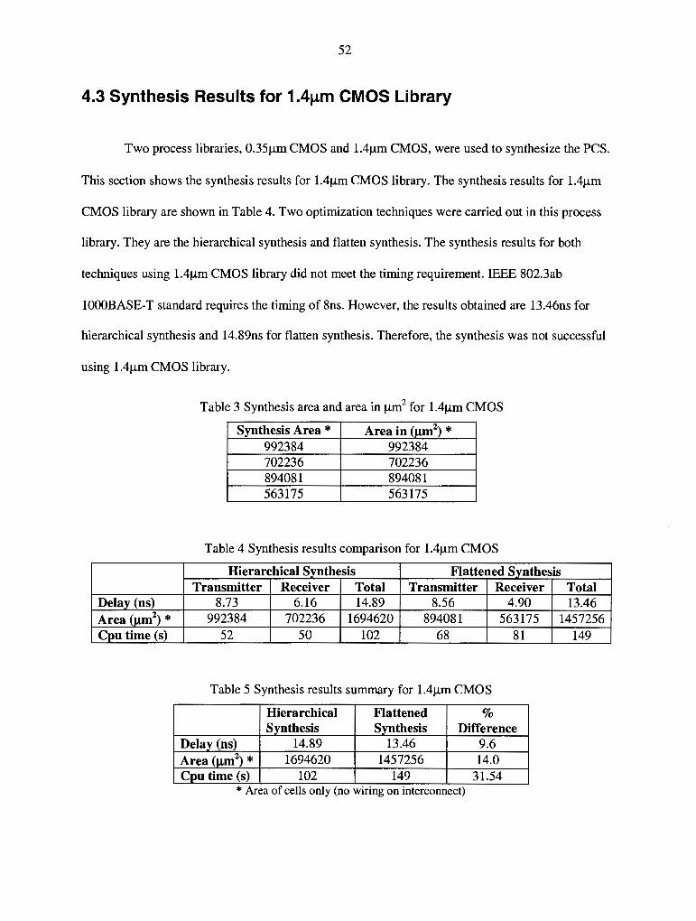
52
4.3 Synthesis Results for 1.4µm CMOS Library
Two process libraries, 0.35µm CMOS and l.4µm CMOS, were used to synthesize the PCS.
This section shows the synthesis results for l.4µm CMOS library. The synthesis results for l.4µm
CMOS library are shown in Table 4. Two optimization techniques were carried out in this process
library. They are the hierarchical synthesis and flatten synthesis. The synthesis results for both
techniques using 1.4µm CMOS library did not meet the timing requirement. IEEE 802.3ab
lO00BASE-T standard requires the timing of 8ns. However, the results obtained are 13.46ns for
hierarchical synthesis and 14.89ns for flatten synthesis. Therefore, the synthesis was not successful
using 1.4µm CMOS library.
Table 3 Synthesis area and area in µm2 for 1.4µm CMOS
Synthesis Area * Area in (um2) * 992384 992384 702236 702236 894081 894081 563175 563175
Table 4 Synthesis results comparison for l.4µm CMOS
Hierarchical Synthesis Flattened Synthesis Transmitter Receiver Total Transmitter Receiver Total
Delay (ns) 8.73 6.16 14.89 8.56 4.90 13.46 Area (um2) * 992384 702236 1694620 894081 563175 1457256 Cpu time (s) 52 50 102 68 81 149
Table 5 Synthesis results summary for l.4µm CMOS
Hierarchical Flattened % Synthesis Synthesis Difference
Delay (ns) 14.89 13.46 9.6 Area (um2) * 1694620 1457256 14.0 Cpu time (s) 102 149 31.54
* Area of cells only (no wiring on interconnect)

53
Table 3 shows the synthesis area and area in µm2• Synthesis area is the area result directly
from the synthesis report. Area in µm2 is the result of the multiplication of the unit area (lµm2) with
the synthesis area. Table 5 shows the summary of the synthesis results and the percentage differences
between different synthesis techniques. The results show that the optimization that was done in the
hierarchical-flattening method has better timing and area. From the area perspective, the flatten
synthesis method gained a better result too. The area for flatten synthesis is 14% better than the area
for hierarchical synthesis. However, the cpu time required to process the flatten synthesis is about
31 % more than the cpu time required to process the hierarchical synthesis.
As the results shown in Table 4 and Table 5, the two methods differ in the result for timing
and area. Hierarchical-flattening is merging all the logic modules into a new cell. It allows the
synthesizer to reduce the critical path delay by optimizing one large module. When the whole design
is flatten into one level, there is no boundary or hierarchy. Therefore, the optimization can be done
more effectively regardless of the module boundaries that exist in hierarchical designs. When
hierarchical optimization technique is used, it groups the modules into a new cell with the lower
modules remain not flatten. The optimization was done at all level of the hierarchy. However, the
optimization effort is only restricted to that level only. That is they still preserve their own structures.
4.4 Synthesis Results for 0.35µm CMOS Library
The synthesis done in 1.4µm CMOS library did not meet the timing requirement of 8ns.
However, the synthesis was successful using the 0.35µm CMOS library. For the synthesis in 0.35µm
CMOS library, the synthesis was carried out again with two different optimization techniques: the
hierarchical synthesis and the flatten synthesis.
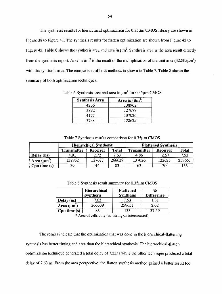
54
The synthesis results for hierarchical optimization for 0.35µm CMOS library are shown in
Figure 38 to Figure 41. The synthesis results for flatten optimization are shown from Figure 42 to
Figure 45. Table 6 shows the synthesis area and area in µm2• Synthesis area is the area result directly
from the synthesis report. Area in µm2 is the result of the multiplication of the unit area (32.805µm2)
with the synthesis area. The comparison of both methods is shown in Table 7. Table 8 shows the
summary of both optimization techniques.
Table 6 Synthesis area and area in µm2 for 0.35µm CMOS
Synthesis Area Area in (µm2)
4236 138962 3892 127677 4177 137026 3738 122625
Table 7 Synthesis results comparison for 0.35µm CMOS
Hierarchical Synthesis Flattened Synthesis Transmitter Receiver Total Transmitter Receiver Total
Delay (ns) 4.91 2.72 7.63 4.86 2.67 7.53 Area (µm2) 138962 127677 266639 137026 122625 259651 Cpu time (s) 39 44 83 63 70 133
Table 8 Synthesis result summary for 0.35µm CMOS
Hierarchical Flattened % Synthesis Synthesis Difference
Delay (ns) 7.63 7.53 1.31 Area (um2) 266639 259651 2.62 Cpu time (s) 83 133 37.59
* Area of cells only (no wiring on interconnect)
The results indicate that the optimization that was done in the hierarchical-flattening
synthesis has better timing and area than the hierarchical synthesis. The hierarchical-flatten
optimization technique generated a total delay of 7.53ns while the other technique produced a total
delay of 7.63 ns. From the area perspective, the flatten synthesis method gained a better result too.

55
The difference in percentage for delay, area and cpu time are shown in Table 8. Flatten synthesis
1.3% better than hierarchical synthesis in terms of delay and 2.62% better than hierarchical synthesis
in terms of area.
As the results show, the two methods differ in the result for timing and area. Hierarchical-
flattening is merging all the logic modules into a new cell. It allows the synthesizer to reduce the
critical path delay by optimizing one large module. When the whole design is flatten into one level,
there is no boundary or hierarchy. Therefore, the optimization can be done more effectively
regardless of the module boundaries that exist in hierarchical designs.
When hierarchical optimization technique is used, it groups the modules into a new cell with
the lower modules remain not flatten. The boundaries of all the hierarchy are remained. The
optimization was done at all levels of the hierarchy. However, the optimization effort is only
restricted to that level only. The optimization effort does not cross over the boundaries. That is they
still preserve their own structures.
The hierarchical-flatten synthesis produces a better result in timing and area. However, there
are two major tradeoffs for using this technique. First, the cpu time required by this technique is
37.59% more the hierarchical synthesis technique. When the whole design is flatten into one level, it
appears as one big design and there is no boundary or hierarchy. Therefore, the optimization is done
more thoroughly regardless of the module boundaries that exist in hierarchical designs. As a result of
that, the cpu time needed is more since the optimization process is more complex. The cpu time
needed for hierarchical synthesis is 83s and for flatten synthesis is 133s.
The other tradeoff for hierarchical-flatten synthesis is the human effort. It takes more effort in
debugging and working on the large flat design. It is very hard to detect the location where the errors
exist in a large design. In hierarchical synthesis, the netlist is divided into smaller pieces. Simulation
could be carried out module by module to check the timing and functional correctness. Debugging is
easier on smaller modules.

56
**************************************** Report : timing
-path full -delay max -max_paths 1
Design transmit Version: 1999.05-2 Date : Mon Jun 26 22:38:51 2000 ****************************************
Operating Conditions: Wire Load Model Mode: enclosed
Startpoint: t2/tx_symb_vector_id_reg[3] (rising edge-triggered flip-flop clocked by GTX_CLK)
Endpoint: gl/csn_l_reg[l] (rising edge-triggered flip-flop clocked by GTX_CLK)
Path Group: GTX_CLK Pa th Type: max
Des/Clust/Port Wire Load Model
transmit GenerateSymbol
Point
clock GTX_CLK
G5K G5K
(rise edge) clock network delay (ideal) t2/tx_symb_vector_id_reg[3]/CK t2/tx_symb_vector_id_reg[3]/Q
(DFFRBN) (DFFRBN)
Library
fs80a_a fs80a_a
t2/tx_symb_vector_id[3] (Xmit_state_machine) gl/tx_symb_vector_id[3] (GenerateSymbol) gl/U768/O (INVl) gl/U649/O (ND2) gl/U648/O (INVl) gl/U646/O (ND2) gl/U647/O (INVl) gl/U601/O (OR2BlL) gl/U889/O (OAI12) gl/U796/O (AN2) gl/U612/O (NR2) gl/U856/O (XNR2) gl/U918/OB (MXL2P) gl/U691/O (INVlL) gl/U855/O (XNR2) gl/U657/O (NR2) gl/csn_l_reg[l]/D (QDFFRSN) data arrival time
clock GTX_CLK (rise clock network delay gl/csn_l_reg[l]/CK library setup time data required time
data required time data arrival time
slack (MET)
edge) (ideal)
(QDFFRSN)
Iner
0.00 1.00 0.00 0.57 0.00 0.00 0.15 0.21 0.23 0.30 0.12 0.13 0.15 0.45 0.16 0.23 0.25 0.43 0.45 0.08 0.00
8.00 1.00 0.00
-0.60
Path
0.00 1.00 1.00 r 1. 57 f 1. 57 f 1. 57 f 1. 73 r 1. 93 f 2.16 r 2.46 f 2.58 r 2. 71 f 2.86 r 3.31 r 3.47 f 3.70 r 3.95 f 4.38 r 4.83 f 4.91 r 4.91 r 4.91
8.00 9.00 9.00 r 8.40 8.40
8.40 -4.91
3.49
Figure 38 Hierarchical synthesis: transmitter timing results for 0.35µm CMOS

57
**************************************** Report : timing
-path full -delay max -max_paths 1
Design receive Version: 1999.05-2 Date : Mon Jun 26 22:39:10 2000 ****************************************
Operating Conditions: Wire Load Model Mode: enclosed
Startpoint: ssl/Scrn_reg[24] (rising edge-triggered flip-flop clocked by elk)
Endpoint: ssl/TD_reg[2] (rising edge-triggered flip-flop clocked by elk)
Path Group: elk Path Type: max
Des/Clust/Port
receive Symb_Sign
Point
Wire Load Model
G5K G5K
clock elk (rise edge) clock network delay (ideal) ssl/Scrn_reg[24]/CK (QDFFRSN) ssl/Scrn_reg[24]/Q (QDFFRSN) ssl/U236/O (XOR2) ssl/U247/O (XOR3) ssl/U225/O (XOR2) ssl/U227/O (XNR2) ssl/TD_reg[2]/D (QDFFRSP) data arrival time
clock elk (rise edge) clock network delay (ideal) ssl/TD_reg[2]/CK (QDFFRSP) library setup time data required time
data required time data arrival time
slack (MET)
Library
fs80a_a fs80a_a
Iner
0.00 1.00 0.00 0.48 0.25 0.39 0.29 0.29 0.00
8.00 1.00 0.00
-0.60
Path
0.00 1.00 1.00 r 1. 48 f 1. 73 r 2.13 f 2.42 r 2.72 f 2.72 f 2.72
8.00 9.00 9.00 r 8.40 8.40
8.40 -2. 72
5.68
Figure 39 Hierarchy synthesis: receiver timing results for 0.35µm CMOS

58
**************************************** Report : area Design : transmit Version: 1999.05-2 Date Mon Jun 26 22:38:52 2000 ****************************************
Library(s) Used:
fs80a_a (File: /home/marwan/SHERLI/synopsys/fs80a_a_core.db)
Number Number Number Number
of of of of
ports: nets: cells: references:
Combinational area: Noncombinational area: Net Interconnect area:
Total cell area: Total area:
31 100
5 5
1944.000000 2292.000000
undefined (Wire load has zero net area)
4236.000000 undefined
Figure 40 Hierarchical synthesis: transmitter area results for 0.35µm CMOS
**************************************** Report : area Design: receive Version: 1999.05-2 Date Mon Jun 26 22:39:11 2000 ****************************************
Library(s) Used:
fs80a_a (File: /home/marwan/SHERLI/synopsys/fs80a_a_core.db)
Number of ports: Number of nets: Number of cells: Number of references:
Combinational area: Noncombinational area: Net Interconnect area:
Total cell area: Total area:
29 53
2 2
1740.000000 2152.000000
undefined (Wire load has zero net area)
3892.000000 undefined
Figure 41 Hierarchy synthesis: receiver area results for 0.35µm CMOS

59
**************************************** Report : timing
-path full -delay max -max_paths 1
Design transmit Version: 1999.05-2 Date : Mon Jun 26 22:48:34 2000 ****************************************
Operating Conditions: Wire Load Model Mode: enclosed
Startpoint: tx_group/t2/tx_symb_vector_id_reg[4] (rising edge-triggered flip-flop clocked by GTX_CLK)
Endpoint: tx_group/gl/csn_l_reg[2] (rising edge-triggered flip-flop clocked by GTX_CLK)
Path Group: GTX_CLK Path Type: max
Des/Clust/Port Wire Load Model
transmit GSK
Point
clock GTX_CLK (rise edge) clock network delay (ideal) tx_group/t2/tx_symb_vector_id_reg[4]/CK tx_group/t2/tx_symb_vector_id_reg[4]/QB U313/O (INVl) Ul04/O (NR2) U184/O (ND2) U228/O (INVl) U293/O (ND2) U303/O (ND2) Ul73/O (INVl) Ul30/O (ND2) U525/O (INV2) U520/OB (MXL2P) U236/O (INVlL) U419/O (XNR2) U235/O (NR2) tx_group/gl/csn_l_reg[2]/D data arrival time
clock GTX_CLK (rise edge) clock network delay (ideal) tx_group/gl/csn_l_reg[2]/CK library setup time data required time
data required time data arrival time
slack (MET)
(QDFFRSP)
(QDFFRSP)
Library
fs80a_a
(DFFRBN) (DFFRBN)
Iner
0.00 1.00 0.00 0.71 0.32 0.14 0.34 0.24 0.21 0.32 0.20 0.11 0.08 0.30 0.37 0.44 0.08 0.00
8.00 1.00 0.00
-0.60
Path
0.00 1.00 1.00 r 1.71 r 2.02 f 2.16 r 2.50 f 2.74 r 2.95 f 3.27 r 3.47 f 3.58 r 3.66 f 3.97 f 4.34 r 4.78 f 4.86 r 4.86 r 4.86
8.00 9.00 9.00 r 8.40 8.40
8.40 -4.86
3.54
Figure 42 Flatten synthesis: transmitter timing results for 0.35µm CMOS

60
**************************************** Report : timing
-path full -delay max -max_paths 1
Design receive Version: 1999.05-2 Date : Mon Jun 26 22:54:01 2000 ****************************************
Operating Conditions: Wire Load Model Mode: enclosed
Startpoint: rx_group/ssl/Scrn_reg[24] (rising edge-triggered flip-flop clocked by elk)
Endpoint: rx_group/ssl/TD_reg[2] (rising edge-triggered flip-flop clocked by elk)
Path Group: elk Path Type: max
Des/Clust/Port Wire Load Model
receive GSK
Point
clock elk (rise edge) clock network delay (ideal) rx_group/ssl/Scrn_reg[24]/CK (QDFFRSN) rx_group/ssl/Scrn_reg[24]/Q (QDFFRSN) U885/O (XOR2) U967/O (XOR3) U791/O (XOR2) U849/O (XNR2) rx_group/ssl/TD_reg[2]/D (QDFFRSP) data arrival time
clock elk (rise edge) clock network delay (ideal) rx_group/ssl/TD_reg[2]/CK (QDFFRSP) library setup time data required time
data required time data arrival time
slack (MET)
Library
fs80a_a
Iner
0.00 1.00 0.00 0.48 0.25 0.39 0.27 0.27 0.00
8.00 1.00 0.00
-0.60
Path
0.00 1.00 1.00 r 1. 48 f 1.73 r 2.13 f 2.40 r 2.67 f 2.67 f 2.67
8.00 9.00 9.00 r 8.40 8.40
8.40 -2.67
5.73
Figure 43 Flatten synthesis: receiver timing results for 0.35µm CMOS
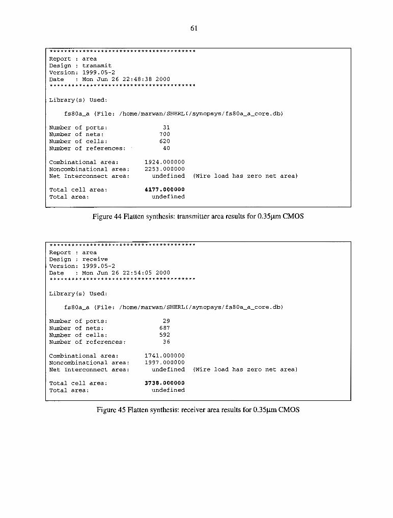
61
**************************************** Report : area Design : transmit Version: 1999.05-2 Date Mon Jun 26 22:48:38 2000 ****************************************
Library(s) Used:
fs80a_a (File: /horne/rnarwan/SHERLI/synopsys/fs80a_a_core.db)
Number of ports: Number of nets: Number of cells: Number of references:
Combinational area: Noncombinational area: Net Interconnect area:
Total cell area: Total area:
31 700 620
40
1924.000000 2253.000000
undefined (Wire load has zero net area)
4177.000000 undefined
Figure 44 Flatten synthesis: transmitter area results for 0.35µm CMOS
**************************************** Report : area Design : receive Version: 1999.05-2 Date Mon Jun 26 22:54:05 2000 ****************************************
Library(s) Used:
fs80a_a (File: /horne/rnarwan/SHERLI/synopsys/fs80a_a_core.db)
Number of ports: Number of nets: Number of cells: Number of references:
Combinational area: Noncombinational area: Net Interconnect area:
Total cell area: Total area:
29 687 592
36
1741.000000 1997.000000
undefined (Wire load has zero net area)
3738.000000 undefined
Figure 45 Flatten synthesis: receiver area results for 0.35µm CMOS

62
4.5 Gate-Level Simulation Results
Design Compiler generated the gate-level description in Verilog HDL format and the delay
information of the gates as Standard Delay Format (SDF) file. This gate-level Verilog HDL
description is in netlist-style description where it describes the design using the corresponding leaf-
level cells of the specific ASIC technology library. Both of the gate-level Verilog HDL and SDF were
then simulated using Verilog-XL compiler. The same original test benches from the previous
behavioral verification can be used because the module and port definitions are preserved through the
translation and optimization processes. The output of the gate-level simulation was compared to the
original output from the Verilog description simulation to ensure correct implementation.
Figure 46 to Figure 50 show the gate-level simulation results for top-level, transmit, data
transmission enable, carrier-sense and receive functions. They are similar to the Verilog simulation
results. Refer to chapter 3 for the explanation of the simulation waveform.
pcs
reset ~l~----+------+-----+------+-----+---------+-~---+-----
TX_ /'u·I EN , L TX ER- H ,.___-----..-----.-------.---------i----------..------.-----
TXD [I EHE[:]jj:J ~-~~-I __ ,___,._~.,.,__,..__,__,,_~ ____ -+------+-----+------+-----+------
~-~--....J
IDLE 80 csreset
ESD ! IDLE
Figure 46 Gate-level simulation results for top-level function
••
L sreset ESD

63
GTX_i CLK
.. 01 Oi Oi& 08 1 0 20 111.0
i tx :, mode~
'
~~ble·LJ L ! I I J .. ffiB:Bi [: RXD 00 80 ss 00 I $SI 80
:seT I I I L baseT ij I I! I L tx
Figure 47 Gate-level simulation results for transmit function
pcs
reset ~~=====;;:------;:=l======+======+======+======+===== link : status!
f--~ ___ ___!:=l=====----i--------i-----v----i--,..-------i-------i-----tx u mode i
~---;::==l=======t=::;---.::=,--;!===~----!"""--'---;:===l=;------;:===I==== 2
IX LJ7i enable:
~rror _j --=--=-==~rn ___________ _ Figure 48 Gate-level simulation results for data transmission enable function

64
~~:et~ ;:=, ====:;---t-----;::=.:======::.======1!>=====:::l=!==========
link status]
f,.----1 -------=+======---i----------i----rtl 1::,·
~ode~ [ . 0
~-LJ LJlJi I ! i~I ~1 nJJl I llln,,,,_ ~nableLJ7 ILJI ~I _I ___ ---+-!----+-----
~mr I niJl~-'-----+-------+-----Figure 49 Gate-level simulation results for carrier sense function
pcs_
reset ~~----+-------+-----t------+------+-----+-'~-----+-----
!~ble U I L =~-~H-+--------------a•-1 ___________ _ ~- ; L ~- -~~---------------------------.--------------
;:seT :""'~"-'-----'
RXD IDLE ao csreset
ESD i IDLE
Figure 50 Gate-level simulation results for receive function
L sreset
ss9 ao ESD

65
4.6 Conclusion
In this chapter, synthesis concepts were explored and the results from synthesis were
discussed. The PCS was synthesized using Synopsys® with two process libraries: 0.35µm CMOS and
l.4µm CMOS. Two synthesis techniques, hierarchical optimization and hierarchical-flattening
optimization, were chosen to compare the area and speed tradeoffs between them. The automation of
the synthesis was accomplished with the creation of synthesis script files. With these script files, the
PCS can be synthesized automatically with any target library desired. The script files are included in
Appendix C. Finally, the gate-level simulation results were shown.
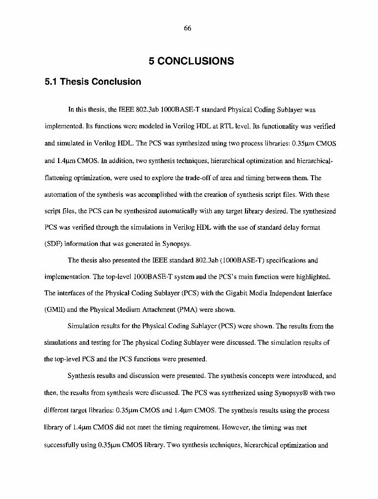
66
5 CONCLUSIONS
5.1 Thesis Conclusion
In this thesis, the IEEE 802.3ab lO00BASE-T standard Physical Coding Sublayer was
implemented. Its functions were modeled in Verilog HDL at RTL level. Its functionality was verified
and simulated in Verilog HDL. The PCS was synthesized using two process libraries: 0.35µm CMOS
and l.4µm CMOS. In addition, two synthesis techniques, hierarchical optimization and hierarchical-
flattening optimization, were used to explore the trade-off of area and timing between them. The
automation of the synthesis was accomplished with the creation of synthesis script files. With these
script files, the PCS can be synthesized automatically with any target library desired. The synthesized
PCS was verified through the simulations in Verilog HDL with the use of standard delay format
(SDF) information that was generated in Synopsys.
The thesis also presented the IEEE standard 802.3ab (lOOOBASE-T) specifications and
implementation. The top-level lO00BASE-T system and the PCS's main function were highlighted.
The interfaces of the Physical Coding Sublayer (PCS) with the Gigabit Media Independent Interface
(GMII) and the Physical Medium Attachment (PMA) were shown.
Simulation results for the Physical Coding Sublayer (PCS) were shown. The results from the
simulations and testing for The physical Coding Sublayer were discussed. The simulation results of
the top-level PCS and the PCS functions were presented.
Synthesis results and discussion were presented. The synthesis concepts were introduced, and
then, the results from synthesis were discussed. The PCS was synthesized using Synopsys® with two
different target libraries: 0.35µm CMOS and l.4µm CMOS. The synthesis results using the process
library of l.4µm CMOS did not meet the timing requirement. However, the timing was met
successfully using 0.35µm CMOS library. Two synthesis techniques, hierarchical optimization and
67
hierarchical-flattening optimization, were chosen to compare the area and speed tradeoffs between
them. The automation of the synthesis was accomplished with the creation of synthesis script files.
With these script files, the PCS can be synthesized automatically with any target library desired.
Finally, the gate-level simulation results were shown.
5.2 Future Work
The PCS of the IEEE 802.3ab standard was implemented and simulated in behavioral and
gate level. This work therefore enables the automatic synthesis of the PCS layer for the IEEE 802.3ab
l0OOBASE-T to any new technology. So, the migration of this design to deep submicron processes
(e.g. 0.18µm and 0.15µm) is possible within a few minutes and without the knowledge of the design
details.

68
APPENDIX A: BIT-TO-SYMBOL MAPPING TABLE
This appendix contains the bit-to-symbol mapping tables. These bit-to-symbol mapping
tables are used for the generating of code-group by the PCS Transmit function. These tables are from
Table 40-1 and Table 40-2 of [16] IEEE 802.3ab/D6.0. Table A.1 shows the bit-symbol mapping for
even subsets. Table A.2 shows the bit-symbol mapping for odd subsets.

69
Table A.1 Bit-Symbol Mapping (Even Subsets)
Sd0 (6:8J= Sd0 (6:8l = Sd0!6:8J = Sd0 (6:8I = [0001 lOHl) 11001 11101
Condition Sd0 (5:0] T A0, TB0 ,TC"' TAD' TB0 .TC0 • T Air TB0 ,TC0 , TAD' TBu,TCn, TD0 TD0 TD0 TD0
Normal 000000 o,o.o,o 0,0,+l,+l O,+l,+1,0 0,+1,0,+I
Normal 000001 -2,0,0,0 -2, 0,+1,+I ·2,+1,+l, 0 -2.+1,0,+I
Normal 000010 0,-2,0,0 0,•2,+l,+I 0,-1,+ I, 0 0,-1, O,+ I
Normal 000011 -2,-2, 0, 0 -2,-2,+l,+I .2,.1,+1, 0 -2.-1, O,+I
Normal OOOlOO 0, 0,-2, 0 0, 0,-1,+l O,+l,-1,0 O,+l,•2,+I
Nl)rmal 000101 -2, 0,-2, 0 -2, 0,-1,+l -2,+1,-1, 0 -2,+ 1,-2,+I
Normal OOOl 10 0,-2.-2, 0 0,2,-1,+l 0,1.-1, 0 0,-1,-2,+1
Normal OOOlll -2,-2,-2, 0 ·2,·2,•l,+I .2,.1,.1, 0 ·2,-1,·2,+l
Normal 001000 0.0,0,.2 0,0,+1,-1 O,+l,+l,-2 O,+l,0,-1
Normal 001001 -2, 0, 0,-2 .2,0,-1,.1 -2,+l,+l,•2 -2,+I, 0,.1
Normal 00!010 0,.2,0,.2 0,-2,+l,•l 0,.1,+1,.2 O,•l, 0,-l
N()rmal OOIOl I -2,-2, 0,-2 .2,.2,+1,.1 -2,-1,+l,-2 .2,.1,0,-1
N()rmal 001 lOO 0, 0,-2,-2 0,0,-1,-1 0,""'1,-1,·2 O,+ 1,-2,-1
Normal 001101 -2, 0,-2,-2 -2. 0,-1,-1 -2,+ 1,-1,-2 -2,+ l,-2,- l
Normal OOll 10 0,-2,-2,-2 0,-2,-1,-1 0,-1,-1.-2 0,- I,-2,-1
N()rmal 001111 -2, .. 2,,..2,-2 -2,-2,-1,-l -2,-1,-1,-2 -2.-1,-2,-1
Normal 010000 +l,+1,-1,+I +l,+l,0,0 +l,0,0,+l +I, 0,-1, 0
Normal 010(.1()1 -1,+l,+I,+I -1,+I, 0,0 -1,0,0,+l -1,0,+l,O
Normal 010010 +l,l,+1,+1 +1,-1,0,0 +1,-2, 0,+I +1,-2,+l. 0
Normal 010011 -1,-1,+!,+l .1,.1,0,0 • l.·2, O,+l -1.-2,+I, 0
Normal 010100 +l,+1.-1,+I +1,+l,•2,0 +I, 0,-2,+I +I, 0,-l, 0
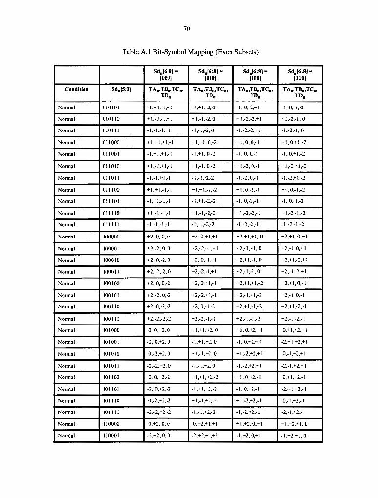
70
Table A.1 Bit-Symbol Mapping (Even Subsetsl_ __
Sd.[6:8j= Sd.(6:8) = Sd.(6:8) = Sd.[6:8) = [000) (011) [1001 (110}
Condition Sd.(5:0) TA., TU.,,TCn, TA.,TO.,TC0 , TA.,TU.,,TCn, TA., TO.,TCn, TD0 TDn TD0 TD0
Normal 010101 -t,+l,-1,+I •l,+l,•2, 0 •l, 0,-2,+l -1. 0,-1, 0
Normal 010110 +l,-1,•l,+I +l,-1;•2; 0 +t,-2,-2,+I +l,-2,-1, 0
Normal 010111 -1,-1,-1,+l -1,-1.-2, 0 -1,-2,-2,+I -1,-2,-1, 0
Normal 011000 +l,+l,+l,•1 +1,+I, 0,-2 +I, 0, 0,-1 +l,0,+1,-2
Normal 011001 -l,+l,+l,-1 -1,+1, 0,-2 -1, 0, 0,-l -1, 0,+1,-2
Normal 011010 +l,-1,+l,-t +l,-1,0,-2 +l,-2, 0,-1 +1,-2,+1,-2
Normal 011011 -1,-1,+1,-1 -1,-1, 0,-2 -1,-2, 0,-l -1,-2,+1,-2
Normal 011100 +l,+l;•l,•l +l,+1,-2,-2 +1,0,·2,•I +l, 0,-1,-2
Normal 011101 -1,+1,-l,•l -1,+l,•2,•2 •l, 0,-2,-1 -1, 0,-1.-2
Normal 011110 +l,-1,-1,-I + 1,-1,-2,-2 + 1,-2,-2,-1 +l,-2,-1,-2
Normal 011111 -1,-1,-1,-1 • t ,-1,-2,-2 -1,-2,-2,-l -1,-2,-1,-2
Normal 100000 +2, o. o. 0 +2, 0,+l,+l +2,+l,+l, 0 +2,+l, O.+l
Normal 100001 +2,-2,0,0 +2,·2,+l,+t +2,-1,+l,0 +2,-1, 0,+l
Normal 100010 +2,0,-2,0 +2, 0,-1,+l +2,+l,•l, 0 +2,+ l,•2,+ 1
Normal 100011 +2,-2,-2.0 +2,-2,• l,+l +2,-1,-1, 0 +2,•l,•2,+l
Normal 100100 +2,0,0,-2 +2, 0,+1,-1 +2,+l,+1,-2 +2,+I, 0,•l
Normal 100101 +2,-2,0,-2 +2,-2,+l,•l +2,•l,+1,-2 +2,-1, 0,-1
Normal 100110 +2,0,-2.-2 +2,0,-1,-1 +2,+1,-1,-2 +2,+l,-2,-1
Normal 100111 +2.-2,-2.-2 + 2,-2.-1,-1 +2,-1,-1,-2 +2,-1,-2,-1
Normal 101000 o. 0,+2, 0 +l,+l,+2, 0 +1,0,+2,+1 0,+1,+2,+l
Normal 101001 •2,0,+2, 0 -1,+l,+2, 0 •I, 0,+2,+l -2,+l,+2,+l
Normal 101010 0,-2,+2,0 +l,-1,+2, 0 +l,•2,+2,+l 0,-1,+2,+l
Normal 10101 l -2,-2,+2, 0 -1,-1,+2, 0 -1,-2,;+2,+ I -2,-1,+2,+l
Normal 101100 0, 0,+2,-2 +1,+l,+2,·2 +I, 0,+2,-1 0,+l,+2,-1
Normal 101101 -2,0,+2,-2 •l,+1;+2,-2 -1, 0,+2,-1 -2,+l,+2,-1
Normal 101110 0,-2,+2,.2 +l,-1,+2,·2 +l,-2,+2,•l 0,-1,+2,-1
Normal 101111 -2,-2,+2,-2 -1,-1;+2,-2 -1,-2,+2,-1 -2,•l,;+2,· I
Normal 110000 0,+2,0,0 0,+2,+l,+l +l,+2, 0,+l +l,+2,+1, 0
Normal 110001 -2,+2,0,0 -2,+2,+l,+I ·l,+2,0,+l •l,+2,+1,0
71
Table A.1 Bit-Symbol Mapping (Even Subsets)
Sd0 (6:8l = Sd0 [6:8] = Sd0 16:81 = Sd0 (6:8) = [OOOJ 10101 11001 [1101
Condition Sd0 15:0) TA.,TB0 .TC0 , TA •• TB0 ,TC0 , TA0 ,TB0 ,TC0 , TA 11,TB0 ,TC0 ,
TD0 TD0 TD0 TDD
Normal 1!0010 0,+2,-2,0 0,+2,-1,+I + I ,+2,-2,+l +l,+2,-1,0
Normal 110011 -2,+2,-2. 0 -2,+2,• I,+ I -1,+2,-2,+1 -l,+2,-1, 0
Normal 110100 0,+2, 0,-2 0,+2,+ 1,-1 +l,+2,0,-1 +l,+2,+l,•2
Normal U0IOI -2,+2, 0,-2 -2,+2.-d,-1 -1,+2, 0,-1 -l,+2,+l,-2
Normal I IOI 10 0,+2,*2,-2 0.+2,-1,-1 +l,+2,-2,-1 +l,+2,-1,-2
Normal ll0l 11 -2,+2,-2,-2 -2,+2,-1,-1 -1,+2,-2,-l -1,+2,-1,-2
l'.onnal 111000 0, 0, 0.+2 +l,+1,0,+2 0,+l,+l,+2 +I, 0,-,.J,+2
Normal 1!1001 -2,0,0,+2 -1,+l,0,+2 -2,+l,+l,+2 -1, 0;H,+2
Nornml l 11010 0,-2, 0,+2 +1,-1, 0,+2 0,-1,+l,+2 +1,-2,+l,+2
Normal l! 1011 -2,-2, 0,+2 -1,-1, 0,+2 •2,• l,+!,+2 -1,-2,+l,+2
Normal 111100 0, 0,-2.+2 +l,+1,-2,+2 0,+1,-1,+2 +I, 0,-1,+2
Normal 111101 -2, 0,-2,+2 -l,+1,-2,+2 -2,+l.-l,+2 .J, 0,-1,+2
Nonna! l l 1110 0,-2,-2,+2 + 1,-1,-2,+2 0,-1,-1,+2 +1,-2.-1.+2
Normal 111111 -2,-2,•2,+2 -1,-1,-2,+2 -2,-1,-1,+2 -1,-2,-1,+2
xmt_err xxxxxx 0,+2,+2,0 +l,+l.+2,+2 +2,+1, .... 1,+2 +2,+l,+2,+I
CSExtend_Err xxxxxx -2,+2,---2,-2 -1,-1,+2,+2 +2,-1,-1,+2 +2,•l,+2,-1
CSExtend xxxxxx +2, 0, 0,+2 +2,+2,+l,+I +l,+2,+2,+I +l,+2,+1,+2
CSReset xxxxxx +2,-2,-2, +2 +2,+2,-l,•I .1,+2,-,.-2,.1 -1,+2,-l,+2
SSDI xxxxxx +2,+2,+2,+2 . . . SSD2 xxx.,xxx +2,+2,+2,-2 . . . ESDI xxxxxx +2,+2,-+2~+2 . . . ESD2_Ext_0 xxxxxx +2,+2,+2,-2 . . . ESD2_Ext_ l xxxxxx +2,+2, -2,+2 . . -ESD2_Ext_2 xxxxxx +2,-2,+2,+2 . . . ESD_Ext _Err xxxxxx -2,+2,+2,+2 . . . Idle/Carrier 000000 0,0,0,0 . . . Extension
Idle/Carrier 000001 -2, 0,0, 0 . . . Extension
72
Table Al Bit-Symbol Mapping (Even Subsets)
Sd.16:81 = = Sd.16:81 = Sd.(6:81 = (000) 10101 llOfl) IHDI
Condition Sd11 f:S:OJ TA1t1TB11,TC11, TA.,,TB11;rc.,, TA11,TBi.~T(~ •• TA_;r111;rc.,, TDu TDll TDu TD11
Idle/Carrier 000()10 0,-2, 0, 0 - - -Extension
ldleJCarrier 000()11 -2,-2, 0, 0 - - -E:xtension
tdlel('.anier 000100 0, 0,-2, 0 - - -E:xtension
tdlei'C'~ier 000101 -2, 0,-1, 0 - - . Extension
tdlei·C~er 0001 lO 0,-2,-1, 0 - - -ExleC1!11on
ldleJC'arrier 000111 -2,-2,-2, 0 - - -Extension
MteiCarrier OOlOOO 0, 0, 0,-2 - . -Extension
tdtei•C~er 001001 -2, 0, 0,-2 - . -Extension
Idle/Carrier OOlOlO 0,-1, 0,-2 - - -Extemion
IdleiCarrier 00l0l1 -2,-1, 0,-2 - - -Extemion
ldlei'Carrier 001100 0, 0.-2,-2 - - -Extensicm
ldlei'Carrier 001101 -2, 0,-2,-2 . . -Extensi(ln
tdkfCarrier 001110 0,-1,-2,-2 - - -Extension
ldleiCarrier 001111 -2,-1,-1,-2 - - -Extension

73
. Tabie A.2 Bit-Symbol Mapping (Odd Subsets)
Sd0 16:81 = Sdu(6:8J = Sd0 (6:8] = Sd0 (6:8I = (001) 10111 I101 J (111]
Condition Sdu(S:OI T A,.,TB,..TC0 , T An, TB11,TC,.. TAmTB11.TCn• TAmTB ... TCn, TO0 TDD TDn TO0
Normal 000000 0, 0, O.+I O. O.+l, 0 0,+1,+J,+l O,+I, 0, 0
Nonna\ 000001 -2. 0, O,+I -2, 0,+1, 0 -2.+l,+l,+l -2,+l. 0, 0
Normal 000010 0,-2, O,+I 0,-2,+I, 0 0,-1,+l,+l 0,-1. 0, 0
Nonna\ 000011 -2.-2, 0,-'-J -2,-2,+I, 0 -2,-1,+l,+I -2.-1. 0, 0
Normal 000(00 0, 0,-2,+I 0,0.-1,0 O,+J,.J,+l 0,+1,-2. 0
Normal 000101 -2. 0,-2,+l -2, 0,-1. 0 -2,+ l ,• l,+ I -2,+l,-2, 0
Normal OOOl lO 0,-2,-2,+! 0,-2,-1. 0 0,-1,• l ,+ I 0,-1,-2, 0
Normal OOOt 11 -2,·2,-2,+ I -2,-2,-1. 0 ·2,•l,•l,+l -2,-1,-2, 0
Normal 001000 0, 0, 0,-1 0, O,+l,-2 0,+ \,+ I,• I O,+I, 0,-2
Nonna! 001001 -2, o. 0.-1 -2.0,+1,-2 -2,+l,+1,-1 -2,+I, 0,-2
Normal 001010 0,-2, 0,-1 0,-2,+ 1,-2 0.-1,+1,.1 0,-1, 0,-2
Nonna! OOIOll -2.-2, 0,-1 -2,-2,+ l ,-2 -2,· I ,+1,-1 -2,.-1. 0,-2
Normal 001100 o. 0,-2.-1 0, 0,-1,-2 O,+ 1,-1,-1 0,+1,-2,•2
Normal 001101 -2. 0,-2,-1 -2, 0,- l,-2 -2.+1,-1.-1 -2,+ 1,-2,-2
Normal 001 l 10 0,-2.-2,-1 0,-2,- l,-2 0,-l,• l,-l 0,-1,-2.,-2
Normal 001! 11 -2.-2,-2.-1 -2,-2.-1.-2 -2,-1,-1,-1 -2,-1,-2.-2
Normal 010000 +l,+1,+1,0 +l,+l,O,+I +1,0,0,0 + l, O,+ l,+l
Normal 010001 -l;H,+1,0 -1,+I, O,+l • I., 0, 0, 0 -l,0,+!,+l
Normal 010010 +1,-1,+I, 0 +1.-1, 0,+1 +l,-2, 0, 0 + l,-2,+ I,+ I
Normal 010011 -1,•l,+l. 0 -1,-1, 0,+ l • J ,-2, 0, 0 .J.,-2,+l,+l
Normal 010100 +l,+1.-1, 0 + !,+ l,-2,+ I +1, 0,-2, 0 +l, 0,-1,+l
Nom1al 010(01 -l.+l,-1. 0 -1,+ L-2,+ I .), 0,-2, 0 -1,0.-1,+I
Normal 010110 +1.-1,-1. 0 -'-1,-1,-2,+l +1,-2,-2, 0 +l,•2.-1,+l
Normal 010111 .J.,-1,-1, 0 -l,-1,•2,+ 1 -1.-2,-2, 0 -1,-2,-! ,+ I
Normal OIIOOO +I,+l,+1,-2 +l,+l,0,-1 -'-I, 0, 0,-2 +1,0,+l,•l
Normal 011001 -1.,+l,+l,•2 -1,+I, 0,-l -1, 0, 0.-2 -1., O.+ l ,• I
Normal 011010 +1,-1,+1,-2 +1,-1,0,-1 +),-2, 0,-2 + 1,-2,+ 1,-1
Nonna! Ol 1011 -l,-1,+l.•2 -1.-1. 0,-1 -1,-2, 0,-2 -1,.-2,+ 1,-1
Normal 011100 +l,+l,-1,•2 + I,+ 1,,2,-l + 1, 0,-2,-2 +l, 0,-J,.J
Normal 011 IOI • 1,+1,-1,-2 -l,+1,-2,-1 -1. 0,-2.-2 -1,0,•l,•l
Nonna! 011110 +1,-1,-1,-2 + 1,-1,•2,· I + 1,-2,-2,-2 + 1,-2,• l ,• l
74
Table A.2 Bit.::Symbol Mapping (Odd SubsetsJ
Sd0 l<i:8l = Sd0 (6:8)= Sd0 (6:8J= Sda(6:8]= IDOIJ (011) 1101) 1111]
Cunditwn Sd0 {S:OJ TA0 ,TB.,TC0 , TAn,TB.,TC., TA,,, TB0 ,TC., TAn,TB.,TC., TD0 TD n TDn TDn
Normal Ollll 1 • 1.-1.-1,-2 -1,-1,-2,-1 -1,-2,-2,-2 -l,•2,-1,•I
Normal 100000 +2,0,0,+l +2, 0,+1, 0 +2,+1,+1,+l +2,+1,0, 0
Normal 100001 +2,-2,0,+l +2,-2,+l,O +2,•l,+l,+l +2,-1,0,0
Normal 100010 +2,0,-2,+l +2,0,-1,0 +2,+1,-1,+l +2,+1,-2,0
Normal 100011 +2,-2,-2,+l +2,-2,-1,0 +2,-1,-1,+I +2,-1,-2,0
Normal 100100 +2, 0, 0,-1 +2,0,+l,•2 +2,+ l,+ I,• l +2,+1,0,•2
Normal 100101 +2,-2, 0,-1 +2,-2,+ l,-2 +2,•l,+1,-1 +2,-1, 0,-2
Normal 100110 +2,0,-2,-l +2,0,-1,-2 +2,+l,•l,•l +2,+1,-2,-2
Normal 100111 +2.-2.-2,-1 +2,-2,-1,-2 +2,-1,-1,-1 +2,-1,-2,-2
Normal 101000 0, 0,+2,+l +l,+l,+2,+l +l, 0,+2, 0 O,+l,+2, 0
Normal 101001 -2,0,+2,+l -1,+l,+2,+l -1,0,+2,0 -2,+t,+2, 0
Nonnal 101010 0,-2,+2,+l +1,-1,+2,+l +l,-2,+2, 0 0,-1,+2, 0
Normal 101011 -2,·2,+2,+ I -1,-1,+2,+1 -1,-2,+2,0 -2,-1,+2, 0
Normal 101100 0, 0,+2,-1 +l,+1,+2,·l +l, 0,+2,-2 0,+l,+2,·2
Normal 101101 -2. 0,+2,-1 •l,+l,+2,•l -1,0,+2,·2 -2,+l,+2,-2
Normal 101110 0,-2,+2,•l +l,•l,+2,-1 + 1,-2,+2,-2 0,-1,+2,-2
Normal 1011 ll -2.-2, +2,-1 -1,-1,+2,-l -1,-2,+2,-2 -2.-1,+2,-2
Normal 110000 0,+2,0,+l 0,+2,+1,0 +l,+2, 0, 0 +l,+2,+1,+l
Normal 110001 -2,+2,0,+I -2,+2,+1, 0 -1,+2,0, 0 -1,+2,+l,+l
Normal 110010 0,+2,-2,+I 0,+2,-1, 0 +l,+2,-2, 0 + l,+2,-1,+l
Normal 110011 ·2,+2,•2,+ I -2,+2,•I, 0 -1,+2,·2, 0 -1,+2,•l,+l
Normal 110100 0,+2,0,-1 0,+2,+l,-2 +l,+2, 0,-2 +l,+2,+1,-1
Normal 110101 -2,+2,. 0,-1 -2,+ 2,+ 1,-2 -t,+2, 0,-2 -1,+2,+1,-1
Normal ll0II0 0,+2,-2,-l o.+2,-1.-2 + l,+2,-2,-2 + l,+2,-1,-1
Normal llOlll -2,+2,-2,-1 -2,+2,•l,•2 -l,+2,-2,-2 -l,+2,-1,•l
Normal 111000 +l,+l,+l,+2 0,0,+l,+2 +l,0,0,+2 O,+l, 0,+2
Normal 111001 -1,+l,+l,+2 -2,0,+1,+2 -1, 0, 0.+2 -2,+I, 0,+2
Normal 111010 +1,-1,+1,+2 0,-2,+l,+2 +l,-2, 0,+2 0,-1. o,+2
Normal 111011 -1,-1,+1,+2 -2,-2,+l,+2 -1,-2,0,+2 -2,-1, 0,+2
75
Table A.2 Bit-Symbol Mapping (Odd Subsets)
Sdnf6:8l = Sdnf6:8) = Sd0 f6:8) = Sdnl6:8) = [0011 10111 11011 [1111
Condition SdnfS:O) TAn,TB0 ,TCn, TA0 ,TBn,TC., TAmTB.,TCm TAmTB.,TCm TD0 TDu TDn TDu
Normal ll 1100 +l,+1,-1,+2 0,0,-1,+2 +I, 0,-2,+2 0,+1,-2,+2
Normal 111101 -1,+1,-t,+2 -2, 0,-1,+2 -1, 0,-2,+2 -2,+l,-2,+2
Normal Jl tl lO +1,-1,-1,+2 0,-2.-1,+2 + I ,-2,-2, + 2 0,-1.-2,+2
Nonna) 1l tt 11 -1,-1,-1,+2 -2,-2,-1,+2 -1,-2,-2,+2 -2,-1,-2,+2
xmt_err xxxxxx +2,+2, 0,+1 0,+2,+1,+2 +l,+2,+2,0 +2,+l,+2, 0
CSExtend_Err xxxxxx +2,+2, -2,-1 -2,+2,-1,+2 -l,+2,+2,-2 +2,-1,+2,-2
CSExtend xxxxxx +2,0,+2,+l +2, 0,+l,+2 +I, 0,+2,+2 +2,+I, 0,-+·2
CSReset xxxxxx +2,-2,+2,-1 +2,-2,-1,+2 -1,-2,+2,+2 +2,-1,-2,+2
76
APPENDIX B: STATE DIAGRAMS
This appendix consists of the following state diagrams:
• PCS Transmit state diagram
• PCS Receive state diagram • PCS Data Transmission Enable state diagram • PCS Carrier Sense state diagram
For details about the variables used and the definition of state diagram, refer to [16).

ST tx_
77
n f pcs_rr~t = ON STD. tx_enable =TRUE. tx_error = FALSE --? ...
SSD1VECTOR SEND IDLE 1000BTtransmit = TRUE
1000BTtransmil -e:= FALSE COL <= 1000BTreceive COL<= FALSE tx_symb_ vector<= SSD 1 tx_symb_vector <= IDLE PUDR PUDR ,L. STD • tx_error = FALSE
Dy T 1~TD ~enable= TRUE. SSD2VECTOR enable = FALSE error= TRUE COL <= 1000BTreceive
SSD1VECTOR,ERROR STD • tx_error"' TRUE tx_symb_ vector<=: SSD2 PUOR
1 00OBTtransmit <=: TRUE .. ~::SIU .. COL<= 1000BTreceive STD
tx_symb_ vector<:=• SSDt ERROR CHECK I PUDR I J. STD , .. tx_enable = TRUE* !tx_enable = TRUE •tx_error = FALSE
SSD2 VECTOR, ERROR .. tx_error = TRUE , COL<=: 1 000BTreceive TRANSMIT ERROR TRANSMIT DATA tx_symb_ vector<=: SSD2 COL <=: t000BTreceive PUDR COL e= 1000BTreceive tx_symb_ vectore=ENCODE(TXD<7:0> tx_symb_ vector e= xmt_err PUDR lmL._ PUDR
I -,1 u .... -... ELSE ! STD*
tx enable = FALSE • tx error = TRUE tx_enable = FALSE. 1st CSReset VECTOR ,I, tx error= TRUE
1000BTtransmit e= FALSE CARRIER EXTENSION COLcz FALSE 1st CS Extension VECTOR
COL cz 1000BTreceive tx_symb_vector <= CS Reset lkV(f = 1032sTMe PUDR IF X0<7: = 0x0 IF (TX0<7:0> = 0x0F)
J. THEN tx_symb_vectore: CSExtend THEN tx_symb_ vector -e:= CEXT STD .[" ELSE tx_symb_ vector= CSExtend_Err ELSE tx_symb_ vector = CEXT _Err
PUDR 2nd CSReset VECTOR
PUDR
STD• tx error= FALSEI !STD• tx_error = TRUE 1uu01:1 !transmit= FALSE COL <=FALSE L_ tx_symb_vectore= CSReset PUDR 2nd CS Extension VECTOR 1 , STD*
STD+ .J, 11..'V.L <=: 1 U\lUl:I I receive D tx_enable = TRUE* IF (TXD<7:0> = 0x0F) tx_error., TRUE
ESD1VECTOR THEN tx_symb_ vector<= CS Extend ,,. STD* 1000BTtransmit = FALSE
ELSE tx_symb_ vector<=: CSExtend_Err C tx_enable = TRUE·
COL ¢::: FALSE PUDR STD* tx_error = FALSE tx_symb_ vector<= ESD1 STD • tx error;: FALS~ 1 STD • tx_error"' TRUE 'II' PUDR 1 tx_enable = FALSE•
STD,L. tx_error = FALSE
ESD2_Ext_0 VECTOR ESD1 VECTOR with Extension
COL <=:FALSE "_uL <= 1_yl!UD , receive IF (TXD<7:0> = 0x0F)
tx_symb_ vector= ESD2_ExL0 THEN tx_symb_ vector<=: ESD1 PUDR ELSE tx_symb_ vector<= ESD_Ext_Err
c!iSTD PUDR
STD • tx_error = FALSE I !sTD. tx_error = TRUE + ESD2 VECTOR with Extension ESD2 Ext 1 VECTOR ~~hf 1,nosTres,Jve 1000BTtransmit <= FALSE ( D<: >;:Qx0}
COL<= FALSE THEN tx_symb_ vector<=: ESD2_ExL2 tx_symb_vector<=: ESD2_Ext_ 1 ELSE tx_symb_ vector<= ESD_Ext_Err PUDR PUDR
~STD ~TD• tx_error = FALSE ell STD• tx_error = TRUE
Fig B.1 PCS Transmit state diagram
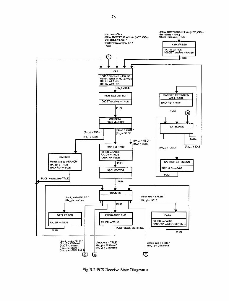
-i•-
78
pcs .. resetc,,QN + (PMA RXSTATUS.indicale (NOT OK) + tink status =FAIL)• 1000BTraceive =FALSE• PUDI
T • l ... IDLE
1 OOOBTreceive <=FALSE rxerror. status= NO.ERROF RX. ER <=FALSE RX.DV <=FALSE
J.(Rlt,,)<'IDLE
NON-IDLE DETECT
1000BTreceive o=TRUE
PUDI
1" CONFIRM
$S02VECTOR
jPMA.,.RXSTATUS.indicaw (NOT .OK}+ Unk .$1a!US =- FAIL)• 1000BTrecewe= TRUE •
UNKFAILEO
RX,.,ER <= TRUE 1 OOOBTrecelve <=FALSE
IPUDI
i CARRIER EXTENSION
with ERROR
RXD<7:0> <=0x1F
PUDI f n ~, EXTEND1NG
(R>\n.tl .t SSD1 • (Rx,,,): SSD1 • (Rx,,} " SSD2
(R><.).tSSD2 I_J L._ ELSE ,,. J (R>t.,1)"' SSD1 •
(Rx.)= SSD2 S801 VECTOR (Rxn,tl e CEXT (Rx,. 1)" IDLE
.... RX.ER <=FALSE RX, DV <= TRUE
BADSSD RXD<7:0> <=0le55 1' 0<error. status <=ERROR
J. PUDI CARRIER EXTENSION
RX ER<=TRUE RXD<7:0> <= OxOE RXD<-7:0> =OxOF
SSD2VECTOR
PUDI I PUDI • ch-Odljdle=TRUE
PUDI .. ,, .. RECEIVE
check end = FALSE • check, end = FALSE • (Rl<,,.1)., xmt,.err
I I I I (Rx.,..,)" DATA
l ELSE
1
DATAERROR PREMATURE END DATA
RX.ER <=TRUE RX ER<=TRUE RX.ER <=FALSE RXD<7.0> <=DECODE(RX..,1)
I PUDI • check.idle=TRUE I PUDI
PUDI
r~e,UTRUE* check.end= TRUE• cileck. end = TRUE • ~ 1·., R&sot• Rx,,) e CSReset • (Rx~,) E CSResot. (Rx,.1)<c CSExtend Rx,,. 'l"' ESD1 • (Rx,..1) <' CSExtend Rx,,., " ESD2.Exl .. 0
C D E
Fig B.2 PCS Receive State Diagram a

79
T T T 1st CSRooet VECTOR 1st CSExtend_Err 1st CSExtend VECTOR
VECTOR rucov ... FALSE RX,,DV <=FALSE RlCDV <:FALSE 1000BTreceive <:FALSE RXD<7:0> <=Ox'1F RXD<7:0> <=0lc:'0F RX,,ER <:FALSE R~ER <=TRUE Rl(ER <=TRUE
PUDI PUDI PUDI
., DELAY 1st CS Err
DELAY 1st CSExt
(Rx"'1)" CSReset •
I (Rxn) e ESD1' (Rx,,.1) e C (Rx ... ,1) e ESD2,,,ExL0 ---ELSE ! ELSE
(Rx,,,1) E CSReset • ... ,. (Rit,,) e ESD1 '
2nd CSExtend_Err , " ,s (Rx,,, 1) E ESD2J:xt,,,0 2nd CSExtend VECTOR VECTOR
2nd CSRoo~t VECTOR RX0<7:0>- <=Ox'1 F
1000BTreceive <=FALSE RX, ER <:FALSE PUDI PUDI
PUDI , .. •• DELAY 2nd CSErr DELAY ,2r1d CSExt
(Rx,..1) e ESD1 • ELSE ELSE (Rx:,..1) e ESD1 •
(Rx.) e ESD2,Ext,0 l r. (Rx.) e ESD2~Exl,,,2 . '· ' ,. ,, .. , ••
ESDtolDLE1 (Rx,.i) e ESD,,Ext,Err • ESD to CEXT,Errt ESDtoCEXT1
1000BTreceive e=FALSE RX,,,ER <=FALSE
(Rx,) e ESD2 ,Exe 1 RXD<7:0> <=0x'1F
PU l~1}E ESD1'
DI (Rx:,.) e ES02,ExL 1 PUOI PUDI ... ,, •r Ir
ESD,Err to IDLE ESD,,,,,Ext 10 IDLE ESD to CEXT,,, Err2 ESDIOCEXT2
RXD<7:0> <=Ox'1F
PUDI I PUDI -' ,. PUDI PUDI p .. ...
A B
Fig B.3 PCS Receive State Diagram b

80
pcs_reset = ON + link_status ¢OK
.,., .. CARRIER SENSE OFF
CRS ¢:;;:FALSE
e =FALSE* (repeater_rnod 1 0OOBTtransrn 1 000BTreceive
it= TRUE)+ =TRUE
~, CARRIER SENSE ON
CRS ¢:;;:TRUE
Fig B .4 PCS Carrier Sense State Diagram
pcs_reset = ON + link_status = FAIL
, r • DISABLE DATA TRANSMISSION
tx_enable <:FALSE tx_error <:FALSE
_mode = SEND_N" tx TX TX
_EN= FALSE* _ER=FALSE
• ,,. ENABLE DATA TRANSMISSION
tx_enable c:TX_EN tx_error<=TX_ER
I I
(repeater_rnode = TRUE + 1 OO0BTtransmit= FALSE) * 1 OO0BTreceive = FALSE
tx_mode = SEND_N tx_mode -i; SEND_N
Fig B.5 PCS Data Transmission Enable State Diagram

81
APPENDIX C: SYNOPSYS SCRIPT FILES
Script files for Synopsys synthesis are included in this appendix. There are three main synthesis script
files:
• compile_separate.scr: in this file, each module is optimized separately. The optimization
process is done in hierarchy.
• compile_one_level.scr: in this file, all modules are combined and flatten to one level. The
optimization process is done in one flatten level.
• default.scr: this file contains the clock constraints and definition.

82
/************************************************************ * canpile.scr * Author: Sher-Li Chew * Script: compile script for Synopsys ************************************************************/
remove_design -all
analyze -format verilog -lib WORK {"/home/sherli/SYNOPSYS/PCS/GenerateSymbol.v"} analyze -format verilog -lib WORK {"/home/sherli/SYNOPSYS/PCS/Storing_values.v"} analyze -format verilog -lib WORK {"/home/sherli/SYNOPSYS/PCS/xmit_state_machine.v"}
analyze -format verilog -lib WORK {"/home/sherli/SYNOPSYS/PCS/data_trans_enable.v"} elaborate Data_trans_enable current_design = Data_trans_enable compile
analyze -format verilog -lib WORK {"/home/sherli/SYNOPSYS/PCS/carrier_sense.v"} elaborate carrier_sense current_design = carrier_sense compile
analyze -format verilog -lib WORK {"/home/sherli/SYNOPSYS/PCS/transmit.v"} elaborate transmit> logs/transmit_elab.log current_design = transmit compile
analyze -format verilog -lib WORK {"/home/sherli/SYNOPSYS/PCS/symb_sign.v"} analyze -format verilog -lib WORK {"/home/sherli/SYNOPSYS/PCS/rcv_state_machine.v"} analyze -format verilog -lib WORK {"/home/sherli/SYNOPSYS/PCS/decoding.v"}
analyze -format verilog -lib WORK {"/home/sherli/SYNOPSYS/PCS/receive.v"} elaborate receive> logs/receive_elab.log current_design = receive compile
/*------------------------------------------------------------------* * * * * * *
save all the designs: transmit, receive, data_trans_enable and carrier_sense. Hierarchy will save all the design in all the hierarchy.
transmit.db will contain all the modules: GenerateSymbol, Xmit_state_machine, and Storing_values.
----------------------------------------------------------------- *!
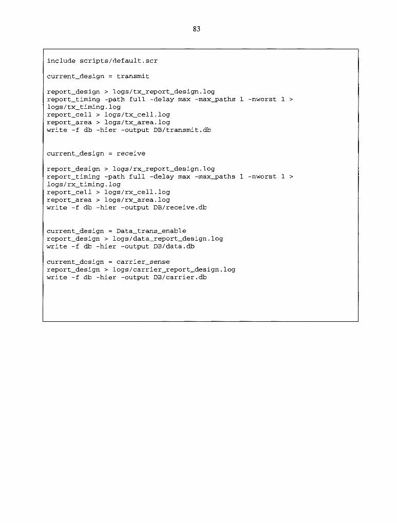
include scripts/default.scr
current_design = transmit
83
report_design > logs/tx_report_design.log report_timing -path full -delay max -max_paths 1 -nworst 1 > logs/tx_timing.log report_cell > logs/tx_cell.log report_area > logs/tx_area.log write -f db -hier -output DB/transmit.db
current_design = receive
report_design > logs/rx_report_design.log report_timing -path full -delay max -max_paths 1 -nworst 1 > logs/rx_timing.log report_cell > logs/rx_cell.log report_area > logs/rx_area.log write -f db -hier -output DB/receive.db
current_design = Data_trans_enable report_design > logs/data_report_design.log write -f db -hier -output DB/data.db
current_design = carrier_sense report_design > logs/carrier_report_design.log write -f db -hier -output DB/carrier.db

84
/***************************************************************** * comple_one_level.scr * Author: Sher-Li Chew * *
This script is to do the optimization for only one hierarchy that is, with all the level flatten.
******************************************************************/
remove_design -all
read -format db {"/home/sherli/SYNOPSYS/DB/transmit.db"} read -format db {"/home/sherli/SYNOPSYS/DB/receive.db"}
current_design = transmit group {"gl" "tl" "t2"} -design_name tx_group -cell_name tx_group current_design = tx_group ungroup { "gl" "tl" "t2"} -flatten compile write -f db -hier -output .. /SYNOPSYS/DB/tx_opt.db
current_design = transmit compile report_design > logs/tx_one_level_report_design.log report_timing -path full -delay max -max_paths 1 -nworst 1 > logs/tx_one_level_timing.log report_cell > logs/tx_cell_one_level.log report_area > logs/tx_area_one_level.log
/*------------------------------------------------------------------*/ current_design = receive group {"ssl" "rsl"} -design_name rx_group -cell_name rx_group current_design = rx_group ungroup {"ssl" "rsl"} -flatten compile write -f db -hier -output .. /SYNOPSYS/DB/rx_opt.db
current_design = receive compile report_design > logs/rx_one_level_report_design.log report_timing -path full -delay max -max_paths 1 -nworst 1 > logs/rx_one_level_timing.log report_cell > logs/rx_cell_one_level.log report_area > logs/rx_area_one_level.log
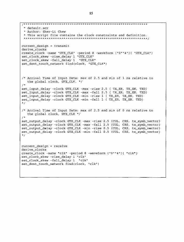
85
/***************************************************************** * default.scr * Author: Sher-Li Chew * This script file contains the clock constraints and definition. *****************************************************************/
current_design = transmit derive_clocks create_clock -name "GTX_CLK" -period 8 -waveform {"0""4"}{ "GTX_CLK"} set_clock_skew -rise_delay 1 "GTX_CLK" set_clock_skew -fall_delay 1 "GTX CLK" set_dont_touch_network find(clock, "GTX_CLK")
/* Arrival Time of Input Data: max of 2.5 and min of 1 ns relative to the global clock, GTX_CLK. */
I* set_input_delay -clock GTX_CLK -max -rise 2.5 { TX _ER, TX _EN, TXD} set_input_delay -clock GTX_CLK -max -fall 2.5 { TX_ER, TX _EN, TXD} set_input_delay -clock GTX_CLK -min -rise 1 { TX_ER, TX_EN, TXD} set_input_delay -clock GTX_CLK -min -fall 1 { TX_ER, TX _EN, TXD} *I
/* Arrival Time of Input Data: max of 2.5 and min of O ns relative to the global clock, GTX_CLK */
/* set_output_delay -clock set_output_delay -clock set_output_delay -clock set_output_delay -clock */
current_design = receive derive_clocks
GTX_CLK -max GTX_CLK -max GTX_CLK -min GTX_CLK -min
-rise 2.5 {COL, CRS, tx_symb_vector} -fall 2.5 {COL, CRS, tx_symb_vector} -rise 0.5 {COL, CRS, tx_symb_vector} -fall 0.5 {COL, CRS, tx_symb_vector}
create clock -name "elk" -period 8 -waveform {"0 1111 4 11 }{ "elk"} set_clock_skew -rise_delay 1 "elk" set_clock_skew -fall_delay 1 "elk" set_dont touch_network find(clock, "elk")

CEXT
CEXT_Err
config
CSExtend
CSExtend_Err
CSReset
86
APPENDIX D: PCS SIGNALS DEFINITIONS
The PCS signals used in this thesis are defined here [16].
A vector of four quinary symbols corresponding to the code-group
generated in idle mode to denote carrier extension.
A vector of four quinary symbols corresponding to the code-group
generated in idle mode to denote carrier extension with error indication.
The config parameter specifies whether the PHY must operate as a
MASTER PHY or as a SLAVE PHY. PMA generates config signal
continuously. PCS and PMA Clock Recovery perform their functions in
MASTER or SLAVE configuration according to the value assumed by
the parameter config.The parameter config can take on one of two
values of the form:
MASTER: This value is continuously asserted when the PHY must
operate as a MASTER PHY.
SLAVE: This value is continuously asserted when the PHY must
operate as a SLAVE PHY.
A vector of four quinary symbols corresponding to the code-group
indicating convolutional encoder reset condition during carrier
extension.
A vector of four quinary symbols corresponding to the code-group
indicating convolutional
encoder reset condition during carrier extension with error indication.
A vector of four quinary symbols corresponding to the code-group

DATA
ESDl
ESD2_Ext_0
ESD2_Ext_l
ESD2_Ext_2
BSD _Ext_Err
IDLE
link_status
87
indicating convolutional encoder reset condition in the absence of
carrier extension.
A vector of four quinary symbols corresponding to the code-group
indicating valid data.
A vector of four quinary symbols corresponding to the first code-group
of End-of-Stream delimiter.
A vector of four quinary symbols corresponding to the second code-
group of End-of-Stream delim-iter
in the absence of carrier extension over the two BSD symbol periods.
A vector of four quinary symbols corresponding to the second code-
group of End-of-Stream delim-iter
when carrier extension is indicated during the first symbol period of the
End-of-Stream delim-iter, but not during the second symbol period.
A vector of four quinary symbols corresponding to the second code-
group of End-of-Stream delim-iter when carrier extension is indicated
during the two symbol periods of the End-of-Stream delim-iter.
A vector of four quinary symbols corresponding to either the first or
second code-group of End-of-Stream delimiter when carrier extension
with error is indicated during the End-of-Stream delimiter.
A sequence of vectors of four quinary symbols representing the special
code-group generated in idle mode in the absence of carrier extension
or carrier extension with error indication.
The link_status parameter can take on one of three values: FAIL,
READY or OK.
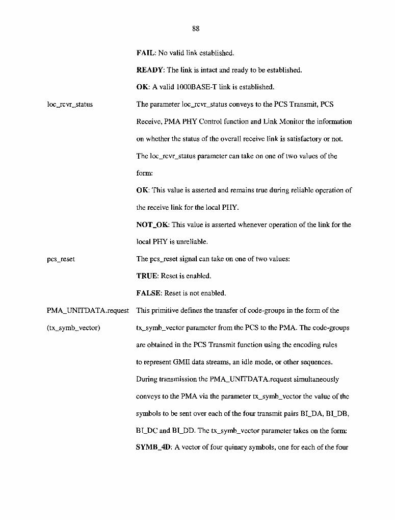
loc_rcvr_status
pcs_reset
88
FAIL: No valid link established.
READY: The link is intact and ready to be established.
OK: A valid lO00BASE-T link is established.
The parameter loc_rcvr_status conveys to the PCS Transmit, PCS
Receive, PMA PHY Control function and Link Monitor the information
on whether the status of the overall receive link is satisfactory or not.
The loc_rcvr_status parameter can take on one of two values of the
form:
OK: This value is asserted and remains true during reliable operation of
the receive link for the local PHY.
NOT_OK: This value is asserted whenever operation of the link for the
local PHY is unreliable.
The pcs_reset signal can take on one of two values:
TRUE: Reset is enabled.
FALSE: Reset is not enabled.
PMA_UNITDATA.request This primitive defines the transfer of code-groups in the form of the
(tx_symb_ vector) tx_symb_ vector parameter from the PCS to the PMA. The code-groups
are obtained in the PCS Transmit function using the encoding rules
to represent GMII data streams, an idle mode, or other sequences.
During transmission the PMA_UNITDATA.request simultaneously
conveys to the PMA via the parameter tx_symb_ vector the value of the
symbols to be sent over each of the four transmit pairs BI_DA, BI_DB,
BI_DC and BI_DD. The tx_symb_ vector parameter takes on the form:
SYMB_4D: A vector of four quinary symbols, one for each of the four

1 000BTreceive
rem_rcvr_status
Rxn
rxerror_status
RX_DV
RX_ER
89
transmit pairs BI_DA, BI_DB, BI_DC and BI_DD. Each quinary
symbol may take on one of the values -2, -1, 0, +1 or +2. The quinary
symbols that are elements of tx_symb_ vector are called, according to
the pair on which each will be transmitted, tx_symb_vector[BI_DA],
tx_symb_ vector[BI_DB], tx_symb_ vector[BI_DC], and
tx_symb_ vector[BI_DD].
The vector of the four correctly aligned most recently received quinary
symbols generated by PCS Receive at time n.
The receiving parameter generated by the PCS Receive function.
Values: TRUE or FALSE
The parameter rem_rcvr_status conveys to the PMA PHY Control
function the information on whether reliable operation of the remote
PHY is detected or not. The loc_rcvr_status parameter can take on one
of two values of the form:
OK: This value is asserted and remains true during reliable operation of
the remote PHY.
NOT_OK: This value is asserted and remains true during unreliable
operation of the remote PHY.
Alias for rx_symb_ vector ( a vector RAn, RBn, RCn, RDn), at time n.
The rxerror_status parameter set by the PCS Receive function.
Values: ERROR or NO_ERROR
The RX_DV signal is from PCS Receive function to the GMII
indicating receive enable.
The RX_ER signal is from the PCS Receive function to the GMII

rx_symb_ vector
RXD[7:0]
SSDl
SSD2
lOOOBTtransmit
TXD[7:0]
tx_enable
tx_error
TX_EN
TX_ER
90
indicating receive error.
A vector of four quinary symbols received by the PMA and passed to
the PCS via the PMA_UNITDATA.indicate primitive.
Value: SYMB_4D
The RXD<7:0> is the eight bits receive data generated by PCS Receive
and passed to the GMII.
A vector of four quinary symbols corresponding to the first code-group
of the Start-of-Stream delimiter.
A vector of four quinary symbols corresponding to the second code-
group of the Start-of-Stream delimiter.
A boolean used by the PCS Transmit Process to indicate whether a
frame transmission is in progress. Used by Carrier Sense process.
Values:
TRUE: The PCS is transmitting a stream
FALSE: The PCS is not transmitting a stream
The TXD<7:0> signal is the eight bits transmit data from the GMII to
the PCS Transmit.
The tx_enable parameter generated by PCS.
Values: TRUE or FALSE
The tx_error parameter generated by PCS Transmit. Values: TRUE or
FALSE
The TX_EN signal is from the GMII to the PCS indicating the transmit
enable. Values: TRUE or FALSE.
The TX_ER signal is from the GMII to the PCS indicating the transmit
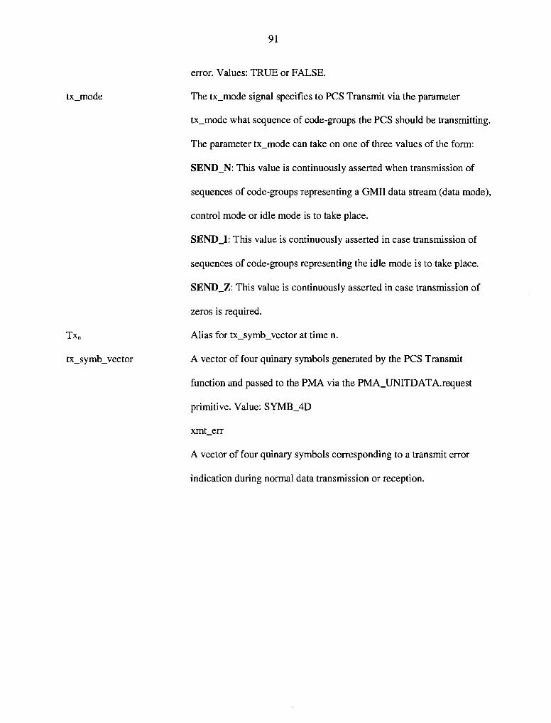
tx_mode
Txn
tx_symb_ vector
91
error. Values: TRUE or FALSE.
The tx_mode signal specifies to PCS Transmit via the parameter
tx_mode what sequence of code-groups the PCS should be transmitting.
The parameter tx_mode can take on one of three values of the form:
SEND_N: This value is continuously asserted when transmission of
sequences of code-groups representing a GMII data stream ( data mode),
control mode or idle mode is to take place.
SEND_I: This value is continuously asserted in case transmission of
sequences of code-groups representing the idle mode is to take place.
SEND_Z: This value is continuously asserted in case transmission of
zeros is required.
Alias for tx_symb_ vector at time n.
A vector of four quinary symbols generated by the PCS Transmit
function and passed to the PMA via the PMA_UNITDATA.request
primitive. Value: SYMB_ 4D
xmt_err
A vector of four quinary symbols corresponding to a transmit error
indication during normal data transmission or reception.

92
REFERENCES [1] Gijung Ahn and Deog-Kyoon Jeong, "A 1.25-GBaud CMOS transceiver with on-chip terminator and voltage mode driver for Gigabit Ethernet lOOOBase-X", International Conference on VLSI and CAD, pp.380-383, Oct. 1999.
[2] Kamran Azadet, "Gigabit Ethernet over Unshielded Twisted Pair Cables", International Symposium on VLSI Technology, Systems, and Applications, pp.167-170, June 1999.
[3] D. Boggs, J. Mogul and C. Kent, "Measured Capacity of an Ethernet: Myths and Reality", Gigabit Ethernet Alliance, Palo Alto, California, 1988.
[4] Dao-Long Chen and M.O. Baker, "A 1.25 Gb/s, 460 mW CMOS transceiver for serial data communication", IEEE International on Solid-State Circuits Conference, pp.242-243, 465, Feb. 1997.
[5] K.J. Christensen, M. Molle, Sifang Li, "Comparison of the Gigabit Ethernet full-duplex repeater, CSMNCD, and 1000/100-Mbps switched Ethernet", 23rd Annual Conference on Local Computer Networks, pp.336-344, Oct. 1998.
[6] Chip Fleming, "A Tutorial on Convolutional Coding with Viterbi Decoding", last accessed July 2000, http://pweb.netcom.com/ ~chip.fNiterbi.html
[7] H. Frazier, H. Johnson, "Gigabit Ethernet: from 100 to 1,000 Mbps", IEEE Internet Computing Vol.31, pp.24-31, Jan.-Feb. 1999.
[8] Gigabit Center, "Gigabit Ethernet Test Center", last accessed July 2000, http://www.gigabitcenter.com/whitepapers.html
[9] Gigabit Ethernet Alliance, "Gigabit Ethernet lOOOBASE-T Whitepaper", Gigabit Ethernet Alliance, Cuppertino, California, 1997.
[10] Gigabit Ethernet Alliance, "Gigabit Ethernet, Accelerating the Standard for Speed", Gigabit Ethernet Alliance, Cuppertino, California, 1997.
[ 11] Gigabit Ethernet Alliance, "Gigabit Ethernet, Accelerating the Standard for Speed", Gigabit Ethernet Alliance, Cuppertino, California, 1998.
[12] E. F. Haratsch, "High-speed VLSI Implementation of Reduced Complexity Sequence Estimation Algorithms with Application to Gigabit Ethernet 1 0OOBase-T", International Symposium on VLSI Technology, Systems, and Applications, pp.171-174, June 1999.
[13] M. Hatamian, 0. E. Agazzi, et al., "Design Considerations for Gigabit Ethernet lOOOBase-T Twisted Pair Transceivers", IEEE Custom Integrated Circuits Conference, pp.335-342, May 1998.
[14] Adam Healey, "lO00BASE-T Technology Overview, InterOperability Lab, last accessed July 2000, http://www.iol.unh.edu/training/ge.html
[15] B. Honary, ''Trellis Decoding of Block Codes", Kluwer Academic Publishers, Boston, Massachusetts, 1997.

93
[16] IEEE Std 802.3ab, "Clause 40 Physical Coding Sublayer (PCS), Physical Medium Attachment (PMA) Sublayer and Baseband Medium, Type lO00BASE-T", IEEE, March 1999.
[17] IEEE Std 802.3z, "Gigabit Ethernet Standard", IEEE Network, Vol.12, pp.6-7, May-June, 1998.
[18] IEEE 802.3ab, "IEEE 802.3ab Task Force", last accessed July 2000, http://grouper.ieee.org/ groups/802/3/ab/index.html
[19] Intel Networking Solution Guides, "Gigabit Ethernet Technical Brief', last accessed July 2000, http://developer.intel.com/network/tech_brief/gigabit_ethernet.htm
[20] Intel Networking Solution Guides, "Gigabit Ethernet Solutions. How lOOOMbps Connectivity is Helping Organizations Meet the Need for Increased Network Performance", last accessed July 2000, http://www.intel.com/network/solutions/ethernet_guide/index.htm
[21] Intel Networking Solution Guides, "Gigabit Ethernet over Copper", last accessed July 2000, http://www.intel.com/network/solutions/copper_guide/index.htm
[22] Intel Online Learning Center (OLC), "Fundamentals of Ethernet Technology", last accessed July 2000, http://channel.intel.com/training/olc/dc/index.htm
[23] InterOperability Lab, "Gigabit Ethernet Training Page", last accessed July 2000, http://www.iol.unh.edu/training/ ge.html
[24] J. Kadambi, I. Crayford, and M. Kalkunte, "Gigabit Ethernet: Migrating to High-Bandwidth LANs", Prentice-Hall, Upper Saddle River, New Jersey, 1998.
[25] Blaine Kohl, "Transitioning to Gigabit Ethernet", Intel Corporation, last accessed July 2000, http://developer.intel.com/update/departments/netcomm/nc04001. pdf
[26] Kurup, Abbasi and Bedi, "It's the Methodology, Stupid!", ByteK Designs Inc, Palo Alto, California, 1998.
[27] P. Kurup, T. Abbasi, "Logic Synthesis Using Synopsys ®",second edition, Kluwer Academic Publisher, Norwell, Massachusetts, 1997.
[28] B. G. Lee and S. C. Kim, "Scrambling Techniques for Digital Transmission", Springer-Verlag, New York, 1994.
[29] Edward A. Lee and David G. Messerschmitt, "Digital Communication", Kluwer Academic Publishers, Boston, Massachusetts, 1994.
[30] J.M. Lee, "Verilog ® Quickstart", Kluwer Academic, Boston, Massachusetts, 1997.
[31] J. Mac he, "An assessment of Gigabit Ethernet as cluster interconnect", First IEEE Computer Society International Workshop on Cluster Computing, pp.36-42, Dec. 1999.
[32] Mick, Colin and Mick Group with Bruce Tolley/3Com and Willem Wery/Intel, "Gigabit Ethernet: Running l000BASE-T over Copper Cabling", Gigabit Ethernet Alliance, Tampa, Florida, 1999.

94
[33] Harl T. Moorthy, S. Lin, G. T. Uehara, "Good Trellises for IC Implementation of Viterbi Decoders for Linear Block Codes", Communications, IEEE Transactions on Vol.45, pp.52 -63, Jan. 1997.
[34] S. Palnitkar, "Verilog HDL: A Guide to Digital Design and Synthesis", Prentice Hall, Mountain View, California, 1996.
[35] John G. Proakis, "Digital Communications", McGraw-Hill, New York, 1983.
[36] M. Sadiku, S. Subramanian, A. Bhadra, "Gigabit Ethernet and ATM in high speed arena", IEEE Southeastcon, pp.295-297, Apr. 1998.
[37] H. Sari, G. Karam, K. Maalej, "Multilevel Continuous Phase Modulation with 4-D Trellis Coding and Linear Receivers", IEEE Global Telecommunications Conference, Vol.3, pp.1274-1278, Nov.-Dec. 1994.
[38] S. Saunders, "Data Communications Gigabit Ethernet Handbook", McGraw-Hill, New York, NY, 1998.
[39] R. Seifert, "Gigabit Ethernet: Technology and Applications for High Speed LANs", Addison-Wesley, Reading, Massachusetts, 1998.
[40] Michael J. S. Smith, "Application-Specific Integrated Circuits", Addison Wesley, Reading, Massachusetts, 1997.
[41] Synopsys®, "CHIP Synthesis", Synopsys, Inc., Mt. View, California, 1996.
[42] Andrew S. Tanenbaum, "Computer Networks", Prentice Hall, Upper Saddle River, New Jersey, 1996.
[43] Lee-Fang Wei, "Trellis-Coded Modulation with Multidimensional Constellations", IEEE Transactions on Information Theory, Vol IT-33, No.4, pp.483-501, July 1987.
[44] Huimin Xia, K. Bataineh, M. Hassoun, J. Kryzak, "A Mixed-signal Behavioral Level Implementation of lOOOBASE-X Physical Layer for Gigabit Ethernet", IEEE International Symposium on Circuits and Systems, Vol. 1, pp.431-434, May-June 1999.