lecture 5 - electrical, computer & energy...
TRANSCRIPT

ECEN 4517 1
Lecture 5ECEN 4517/5517
Buck converter
Battery charge controller
Peak power tracker
Experiment 3

ECEN 4517 2
Due dates
Next week:Exp. 3 part 2 prelab assignment: MPPT algorithm
Late assignments will not be accepted.Due at noon next Tuesday in D2L
This week:Finish Exp. 3 part 1!

ECEN 4517 3
Exp. 3, Part 1Demonstrate buck power stage

ECEN 4517 4
Heatsinks
The power semiconductors generally require heatsinks. Example—from the HUF35371 (our 55 V, 34 mΩ MOSFET) datasheet:
Multiply thermal resistance by power loss to find temperature rise
With no heatsink, the thermal resistance is quite high (62˚C/W)With a 25˚C ambient temperature and no heatsink, this device will reach the rated limit of 175˚C if its power dissipation is
Ploss = (175˚C – 25˚C)/(62˚C/W) = 2.4 WA heatsink can lower this temperature rise considerably. The junction-to-case thermal resistance is only 1.6 ˚C/W.
For reliability reasons, we like to limit temperature rises to much lower values— perhaps a few tens of ˚C

ECEN 4517 5
Heatsinks:Thermal model
The parts kit heatsinks:
From the graph, 2.4 W of loss causes a 30 ˚C rise, which would make the heatsink operate at 55˚C for a 25˚C ambient.Plus junction-to-case temperature rise of (1.6˚C/W)(2.4 W) = 4˚C
Thermal equivalent circuit model
ECEN 4517 6
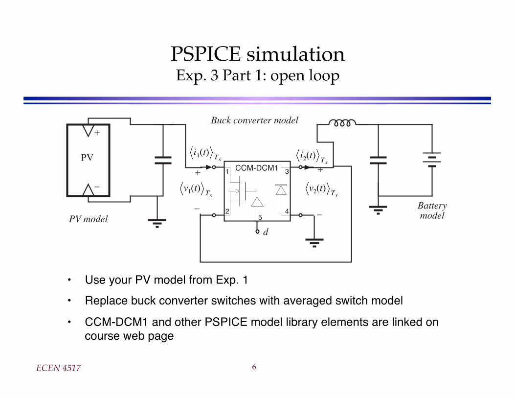
PSPICE simulationExp. 3 Part 1: open loop
Buck converter model
PV
+
–
i2(t) Ts
v2(t) Tsv1(t) Ts
i1(t) Ts
d
+
–
+
–
1
2
3
45
CCM-DCM1
PV modelBatterymodel
• Use your PV model from Exp. 1
• Replace buck converter switches with averaged switch model
• CCM-DCM1 and other PSPICE model library elements are linked oncourse web page
ECEN 4517 17
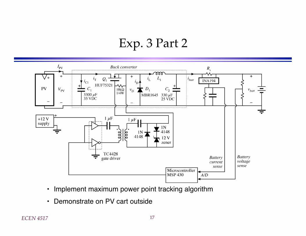
Exp. 3 Part 2
• Implement maximum power point tracking algorithm
• Demonstrate on PV cart outside
ECEN 4517 14
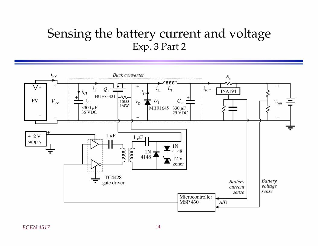
Sensing the battery current and voltageExp. 3 Part 2

ECEN 4517 15
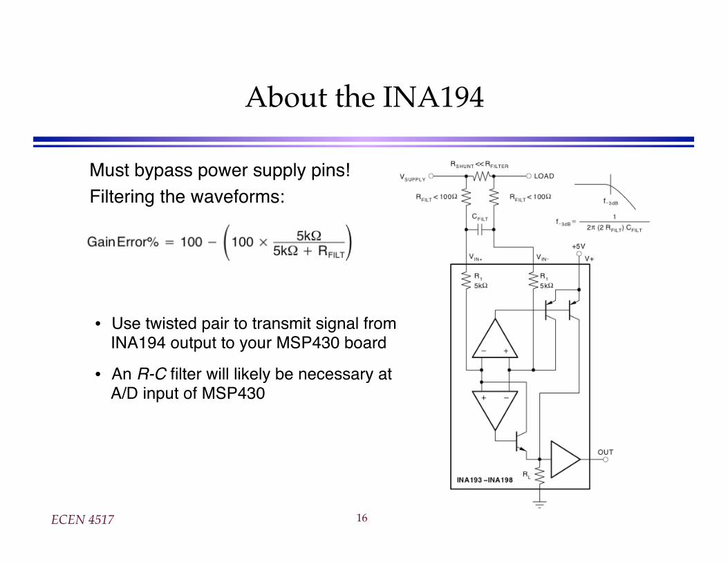
INA194 High-side current sense IC
INA194: gain = 50V/V
ECEN 4517 16
About the INA194
Must bypass power supply pins!Filtering the waveforms:
• Use twisted pair to transmit signal from INA194 output to your MSP430 board
• An R-C filter will likely be necessary at A/D input of MSP430

ECEN 4517 18
Maximum Power Point Tracking
Automatically operate the PV panel at its maximum power point
I-V curve with partial shading
Power vs. voltage
Some possible MPPT algorithms:
• Perturb and observe
• Periodic scan
• Newtonʼs method, or related hill-climbing algorithms
• What is the control variable? Where is the power measured?
Next weekʼs prelab assignment: propose a MPPT algorithm, submit flowchart/block diagram

ECEN 4517! 14!
Example MPPT: Perturb and Observe • A well-known approach"• Works well if properly tuned"• When not well tuned, maximum power
point tracker (MPPT) is slow and canget confused by rapid changes inoperating point"
• A common choice: “control” is switchduty cycle"
Basic algorithm!!Measure power"Loop:"• Perturb the operating point in
some direction"
• Wait for system to settle"
• Measure power"
• Did the power increase?"
Yes: retain direction for next perturbation"
N: reverse direction for next perturbation"
Repeat"

ECEN 4517 20
Example MPPT: Sweep
Start at V = minimum PV voltage. Set Pmax = 0.Loop:
Wait for system transients to settle
Measure power P. Is P > Pmax?Yes: set Pmax = P, Vopt = V
Increase V by one step
Repeat until V = VocSet V = Vopt. Wait some time, then sweep again.

ECEN 4517 20
ADC10: The 10-Bit A/D Converterof the MSP430
Key features:
• Multiplexed inputs
• Sample and hold circuit
• Successive approximation register, driven by selectable clock
• Selectable reference sources
• Buffered output memory
• 10 bit or 8 bit conversion
Divider/1 .. /8
:1:4:64
000110
10-bit ADC Core
VR- VR+
Convert
SampleandHold
S/H
0011 0110
1 0
0000000100100011010001010110011110001001101010111100110111101111
Sample Timer/4 .. /1024
1
0
1
0
Sync1
0
1
0
00
11
01
10
MODOSC from UCS
ACLK
MCLK
SMCLK
00
11
01
10
ADC10SC
3 inputsfrom Timers
Data Format
ADC10MEM
10-bit WindowComparator
VSS
Vcc
VREF 1.5 / 2.0 / 2.5 V from shared reference
ADC10SR
ADC10ON
ADC10SREFx
ADC10SREF2
Auto
ADC10CONSEQx
ADC10INCHx
A0A1A2A3A4A5A6A7
A15A14A13A12
TempSenseBatt.Monitor
VEREF+
VEREF-
ADC10DIVx
ADC10PDIVx
ADC10SSELx
ADC10BUSYADC10SHP
ADC10MSC
ADC10SHTx
SHI
ADC10ISSH
SAMPCON
ADC10MSC
ADC10HIx
ADC10LOx
ADC10DF
To Interrupt Logic
01
10
ADC10CLK
ReferenceBuffer
ADC10SHSx
A8A9

ECEN 4517 21
Successive Approximations
Reference: John H. Davies, MSP430 Microcontroller Basics, Elsevier, 2008, ISBN 987-7506-8276-3.
• After the input signal has been sampled, the 10-bit SAR requires 11 clock cycles to generate an output
• Compare analog input with references
• The MSP430 uses a switched capacitor scheme to perform the comparisons
• See MSP430x5xx Family User’s Guide, Ch. 27

ECEN 4517 22
Capacitor bypassing is required
What the User’s Guide recommends:
Also need capacitance at analog input pin

ECEN 4517 23
Setting up the A/D Converter ADC10
// Configure ADC10ADC10CTL0 = ADC10SHT_2 + ADC10ON; // sample time of 16 clocks, turn on
// use internal ADC 5 MHz clockADC10CTL1 = ADC10SHP + ADC10CONSEQ_0; // software trigger to start a sample
// single channel conversionADC10CTL2 = ADC10RES; // use full 10 bit resolutionADC10MCTL0 = ADC10SREF_1+ADC10INCH_5; // ADC10 ref: use VREF and AVSS
// input channel A5 (pin 10)// Configure internal reference VREFwhile(REFCTL0 & REFGENBUSY); // if ref gen is busy, waitREFCTL0 |= REFVSEL_0 + REFON; // select VREF = 1.5 V, turn on_delay_cycles(75); // delay for VREF to settle
The above code sets up the 10-bit ADC with A5 as its only input, with 1.5 V giving a reading of 210 – 1, and 0 V giving a reading of 0. Each reading will employ a sampling window of 16 ADC clocks = 3.2 μsec.

ECEN 4517 24
Sampling the ADC input
ADC10CTL0 |= ADC10ENC + ADC10SC; // sampling and conversion startwhile(ADC10CTL1 & ADC10BUSY); // wait for completionX = ADC10MEM0; // ADC10MEM0 contains result
The above code is simple and a good start. See CCS5 code examples for use of interrupts that do not require the processor to wait during the conversion time.