lecture 38 high speed nyquist adcs - aicdesign.org€¦ · lecture 38 – high speed nyquist adcs...
TRANSCRIPT

Lecture 38 – High Speed Nyquist ADCs (6/26/14) Page 38-1
CMOS Analog Circuit Design © P.E. Allen - 2016
LECTURE 38 – HIGH SPEED NYQUIST ADCS
LECTURE ORGANIZATION
Outline
• Parallel/flash ADCs
• Interpolating and averaging
• Folding
• High-speed, high-resolution ADCs
• Time-interleaved ADCs
CMOS Analog Circuit Design, 3rd Edition Reference
Pages 573-588

Lecture 38 – High Speed Nyquist ADCs (6/26/14) Page 38-2
CMOS Analog Circuit Design © P.E. Allen - 2016
PARALLEL/FLASH ADCs
Parallel/Flash ADC Architecture
• The notation, vin*(t), means the signal is sampled and held.
• The sample and hold function can be incorporated into the comparators
• The digital words designated as di form a thermometer code
060928-01
Voltage
Scaling
Network
creating
all possible
discrete
analog
voltages
VREF
V1
V2
V3
V4
V2N-1
Sample
and Hold
Circuit
vin(t)
vin*(t)
2N-1
Compar
ators
d1
d2
d3
d4
d2N-1
2N-1
to N
Decoder
b1
b2
b3
bN
Phase 1 Phase 2
One Clock Period, T
Analog
Input
Digital
Word
Output

Lecture 38 – High Speed Nyquist ADCs (6/26/14) Page 38-3
CMOS Analog Circuit Design © P.E. Allen - 2016
A 3-bit, parallel ADC
General Comments:
• Fast, in the first phase of the clock the
analog input is sampled and applied to the
comparators. In the second phase, the
digital encoding network determines the
correct output digital word.
• Number of comparators required is 2N-1
which can become large if N is large
• The offset of the comparators must be less
than ±VREF/2N+1
• Errors occur as “bubbles” in the
thermometer code and can be corrected
with additional circuitry
• Typical sampling frequencies can be as
high as 1000MHz for 6-bits in sub-micron CMOS technology.
1R+-
1R+-
0R
+-
0R
+-
0R
+-
0R
+-
0R
+-
VREF Vin*=0.7VREF
R
2N-1
to N
encoder
Output
Digital
Word
101
0.875VREF
0.750VREF
0.625VREF
0.500VREF
0.375VREF
0.250VREF
0.125VREF
Fig.10.8-1
Lecture 38 – High Speed Nyquist ADCs (6/26/14) Page 38-4
CMOS Analog Circuit Design © P.E. Allen - 2016
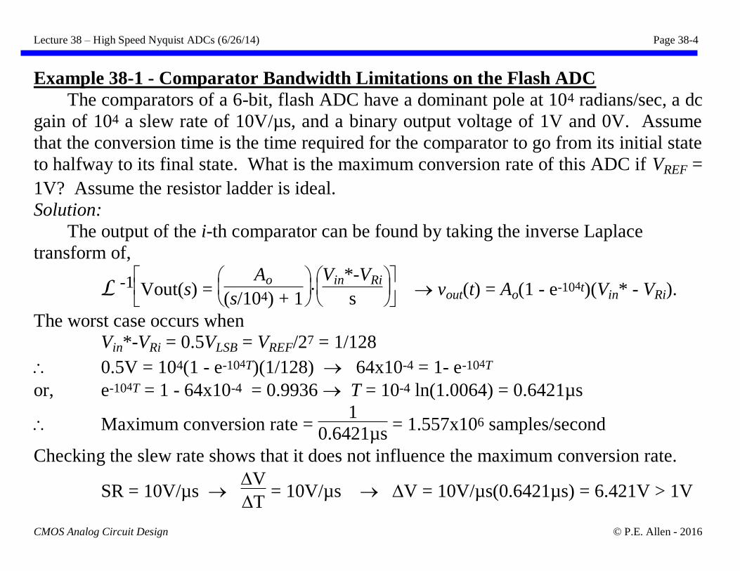
Example 38-1 - Comparator Bandwidth Limitations on the Flash ADC
The comparators of a 6-bit, flash ADC have a dominant pole at 104 radians/sec, a dc
gain of 104 a slew rate of 10V/µs, and a binary output voltage of 1V and 0V. Assume
that the conversion time is the time required for the comparator to go from its initial state
to halfway to its final state. What is the maximum conversion rate of this ADC if VREF =
1V? Assume the resistor ladder is ideal.
Solution:
The output of the i-th comparator can be found by taking the inverse Laplace
transform of,
L -1
Vout(s) =
Ao
(s/104) + 1·
Vin*-VRi
s → vout(t) = Ao(1 - e-104t)(Vin* - VRi).
The worst case occurs when
Vin*-VRi = 0.5VLSB = VREF/27 = 1/128
0.5V = 104(1 - e-104T)(1/128) → 64x10-4 = 1- e-104T
or, e-104T = 1 - 64x10-4 = 0.9936 → T = 10-4 ln(1.0064) = 0.6421µs
Maximum conversion rate = 1
0.6421µs = 1.557x10⁶ samples/second
Checking the slew rate shows that it does not influence the maximum conversion rate.
SR = 10V/µs → V
T = 10V/µs → V = 10V/µs(0.6421µs) = 6.421V > 1V

Lecture 38 – High Speed Nyquist ADCs (6/26/14) Page 38-5
CMOS Analog Circuit Design © P.E. Allen - 2016
Signal Delay in High Speed Converters
Assume that clocked comparators are used in a 500MHz sampling frequency ADC
of 8-bits. If the input frequency is 250MHz with a peak-to-peak value of VREF, the
clock accuracy must be
t V
Vp =
VREF/2N+1
2f(0.5VREF) =
1
29··f ≈ 2.5ps
Since electrical signals travel at approximately 50µm/ps for metal on an IC, each metal
path from the clock to each comparator must be equal to within 125µm to avoid LSB
errors due to clock skew. Therefore, must use careful layout to avoid ADC inaccuracies
at high frequencies.
An equal-delay clock distribution system for a 4-bit parallel ADC:
1 2 3 4 5 6 7 8 9 10 11 12 13 14 15 16
Clock
Generator
Fig.10.8-2BComparators

Lecture 38 – High Speed Nyquist ADCs (6/26/14) Page 38-6
CMOS Analog Circuit Design © P.E. Allen - 2016
Other Errors of the Parallel ADC
• Resistor string error - if current is drawn from the taps to the resistor string this will
create a “bowing” effect on the voltage. This can be corrected by applying the correct
voltage to various points of the resistor string.
• Input common mode range of the comparators - the comparators at the top of the string
must operate with the same performance as the comparators at the bottom of the string.
• Kickback or flashback - influence of rapid transition changes occurring at the input of a
comparator. Can be solved by using a preamplifier or buffer in front of the
comparator.
• Metastability - uncertainty of the comparator output causing the transition of the
thermometer code to be undetermined.

Lecture 38 – High Speed Nyquist ADCs (6/26/14) Page 38-7
CMOS Analog Circuit Design © P.E. Allen - 2016
INTERPOLATING AND AVERAGING
Illustration of a 3-bit interpolating ADC using a factor of 4 interpolation
Comments:
• Capacitive loading at the input is reduced from 8 comparators to two amplifiers.
• The comparators no longer need a large ICMR
• V1 and V2, are interpolated through the resistor string and applied to the comparators.
• Because of the amplification of the input amplifiers and a single threshold, the
comparators can be simple and are often replaced by a latch.
• If the dots in Fig. 10.8-4 are not equally spaced, INL and DNL will result.
VDD
Vth
VREF0
0
V2a
V2
V2b
V2c
V1a
V1
V1b
V1c
0.5VREFVin
Volts
Comparator
Threshold
1 2 3 4 5 6 7 8
Fig.10.8-4

Lecture 38 – High Speed Nyquist ADCs (6/26/14) Page 38-8
CMOS Analog Circuit Design © P.E. Allen - 2016
A 3-Bit Interpolating ADC with Equalized Comparator Delays
One of the problems in voltage (passive) interpolation is that the delay from the amplifier
output to each comparator can be different due to different source resistance.
Solution:

Lecture 38 – High Speed Nyquist ADCs (6/26/14) Page 38-9
CMOS Analog Circuit Design © P.E. Allen - 2016
Active Interpolation
Example of a 3 level current interpolation:
This type of interpolation works well with current processing, i.e., current comparators.

Lecture 38 – High Speed Nyquist ADCs (6/26/14) Page 38-10
CMOS Analog Circuit Design © P.E. Allen - 2016
Interpolation using Amplifiers
Vo3 = K(Vy – Vx) which is between Vy and Vx.
060928-03
+
-
+
-
+
-
+
-
+
-
+
-
+
-
+
-
+
-
+
-
VR,j+1
VR,j
Vin PreamplifiersInterpolating
Amplifiers
Aj+1
Aj
Vy
Vx Vo1
Vo3
Vo2

Lecture 38 – High Speed Nyquist ADCs (6/26/14) Page 38-11
CMOS Analog Circuit Design © P.E. Allen - 2016
Averaging†
In many cases, the comparators
consist of a number of pre-
amplifiers followed by a latch.
Averaging is the result of
interconnecting the outputs of
each stage of amplifiers so that
the errors in one amplifier
chain are balanced out by
adjacent amplifier chains.
Result: The offsets are reduced
allowing the transistors to be
made smaller and therefore
reducing the parasitics
increasing the speed of the
ADC.
† P.C.S. Scholtens and M. Vertregt, “A 6-b 1.6-Gsample/s Flash ADC in 0.18 µm CMOS Using Averaging Termination, IEEE J. of Solid-State
Circuits, vol. 37, no. 12, Dec. 2002, pp. 1599-1609.
VDD
Termination
Resistors
Termination
Resistors
A11
AN-2,1
A21
AN-1,1
VDD
Termination
Resistors
Termination
Resistors
A12
AN-2,2
A22
AN-1,2
VDD
Termination
Resistors
Termination
Resistors
A13
AN-2,3
A23
AN-1,3
060928-04

Lecture 38 – High Speed Nyquist ADCs (6/26/14) Page 38-12
CMOS Analog Circuit Design © P.E. Allen - 2016
Analog Front End of an ADC using Averaging

Lecture 38 – High Speed Nyquist ADCs (6/26/14) Page 38-13
CMOS Analog Circuit Design © P.E. Allen - 2016
FOLDING
Folding Analog-Digital Converters
Allows the number of comparators to be reduced below the value of 2N-1.
Architecture for a folded ADC:
Operation:
The input is split into two or more parallel paths.
• First path uses a coarse quantizer to quantize the signal into 2n1 values
• The second path maps all of the 2n1 subranges onto a single subrange and applies this
analog signal to a fine quantizer of 2n2 subranges.
Thus, the total number of comparators is 2n1-1 + 2n2-1 compared with 2n1+n2-1 for a
parallel ADC.
I.e., if n1 = 2 and n2 = 4, the folding ADC requires 3 + 15 = 18 compared with 63
comparators.
PreprocessorCoarse
Quantizer
Folding
Preprocessor
Fine
Quantizer
Encoding
Logicv*in
Digital
Output
n1
bits
n2
bits
n1+n2
bits
120525-01
Lecture 38 – High Speed Nyquist ADCs (6/26/14) Page 38-14
CMOS Analog Circuit Design © P.E. Allen - 2016
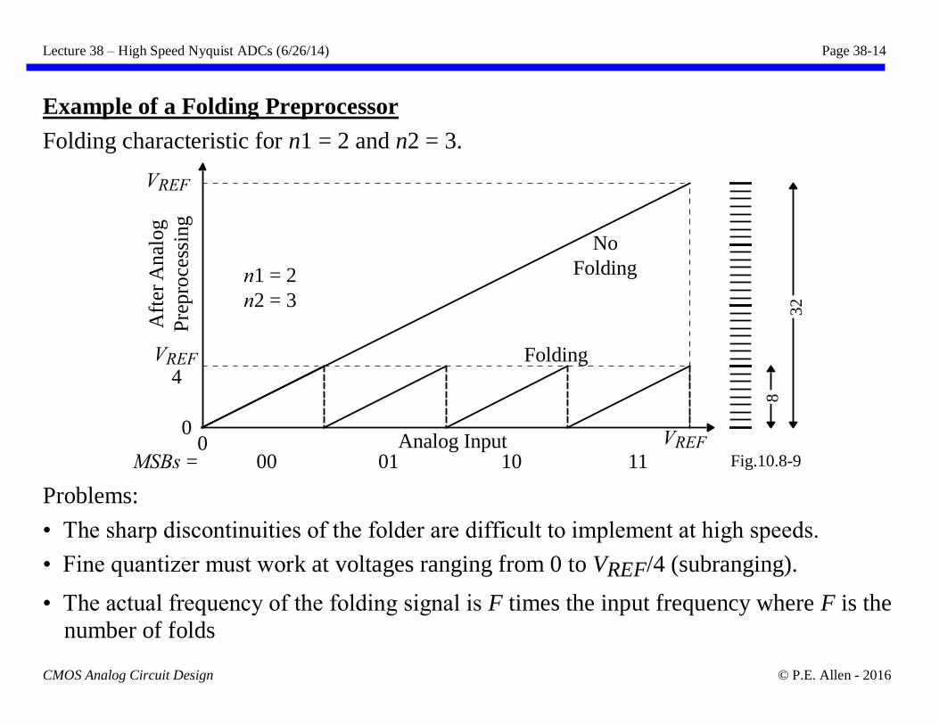
Example of a Folding Preprocessor
Folding characteristic for n1 = 2 and n2 = 3.
Problems:
• The sharp discontinuities of the folder are difficult to implement at high speeds.
• Fine quantizer must work at voltages ranging from 0 to VREF/4 (subranging).
• The actual frequency of the folding signal is F times the input frequency where F is the
number of folds
8
32
No
Folding
Folding
Analog Input
Aft
er A
nal
og
Pre
pro
cess
ing
MSBs = 00 01 10 11
n1 = 2
n2 = 3
VREF
VREF4
00 VREF
Fig.10.8-9
Lecture 38 – High Speed Nyquist ADCs (6/26/14) Page 38-15
CMOS Analog Circuit Design © P.E. Allen - 2016
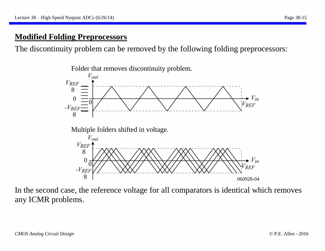
Modified Folding Preprocessors
The discontinuity problem can be removed by the following folding preprocessors:
In the second case, the reference voltage for all comparators is identical which removes
any ICMR problems.
060928-04
Vin
Vout
Multiple folders shifted in voltage.
Vin
Vout
VREF
8
0
-VREF
8
VREF
8
0
-VREF
8
VREF
VREF
0
0
Folder that removes discontinuity problem.

Lecture 38 – High Speed Nyquist ADCs (6/26/14) Page 38-16
CMOS Analog Circuit Design © P.E. Allen - 2016
A 5-Bit Folding ADC Using 1-Bit Quantizers (Comparators)
Block diagram:
Comments:
• Number of comparators is 7 for the fine quantizer and 3 for the coarse quantizer
• The zero crossings of the folders must be equally spaced to avoid linearity errors
• The number of folders can be reduced and the comparators simplified by use of
interpolation

Lecture 38 – High Speed Nyquist ADCs (6/26/14) Page 38-17
CMOS Analog Circuit Design © P.E. Allen - 2016
Folding Circuits
Implementation
of a times 4
folder used
in a 3-bit
quantizer:
Comments:
• Horizontal shifting is achieved by connecting V1 through V8 to different points on the
voltage scaling resistor string.
• Folding and interpolation ADCs offer the most resolution at high speeds (≈8 bits at
500MHz)
060928-06
V1 V2 V8
VDD
Folding
Outputs
Vin
+VREF
V1
V2
V3
V8
Vout - +
Vout
V7
Vin
I I I I
RL RL
R/8
0
+IRL
-IRL
VREF
I
R/8R/8R/8R/8
R/8
R/8R/8R/8R/8R/8R/8R/8R/8
R/8
V1 V2 V3 V4 V5 V6 V7 V8
To com-
parator
R/8R/8
R/8R/8
R/8
R/8R/8R/8R/8R/8

Lecture 38 – High Speed Nyquist ADCs (6/26/14) Page 38-18
CMOS Analog Circuit Design © P.E. Allen - 2016
HIGH-SPEED, HIGH-RESOLUTION ADCs
Multiple-Bit, Pipeline Analog-Digital Converters
A compromise between speed and resolution is to use a pipeline ADC with multiple
bits/stage.
i-th stage of a k-bit per stage pipeline ADC with residue amplification:
Residue voltage = Vi-1 -
b0
2 +
b1
22 + ··· +
bk-2
2k-1 +
bk-1
2k VREF
Potential specifications range from 100-300 Msps and 10 to 14 bits.
061002-02
k-bit
ADC
k-bit
DAC
k-bits
S/HVREF VREF
S
Av =2k
+
-
i-th stage
Vi-1
Clock
Vi
Residue
k-bit
ADC
k-bit
DAC
k-bits
S/HVREF VREF
S
Av =2k
+
-
i+1-th stage
Clock
Vi+1
Residue

Lecture 38 – High Speed Nyquist ADCs (6/26/14) Page 38-19
CMOS Analog Circuit Design © P.E. Allen - 2016
A 3-Stage, 3-Bit Per Stage Pipeline ADC
Illustration of the operation:
Converted word is 011 111 001
Comments:
• Only 21 comparators are required for this 9-bit ADC
• Conversion occurs in three clock cycles
• The residue amplifier will cause a bandwidth limitation,
GB = 50MHz → f-3dB = 50MHz
23 6MHz
000001
011010
100101110111
000001
011010
100101110111
000001
011010
100101110111
Clock 1
Stage 1
Clock 2
Stage 2
Clock 3
Stage 3
Digital output = 011 111 001
MSB LSB Fig.10.8-14
VREF
VREF
2
0 Time
Vo
ltag
e
Lecture 38 – High Speed Nyquist ADCs (6/26/14) Page 38-20
CMOS Analog Circuit Design © P.E. Allen - 2016
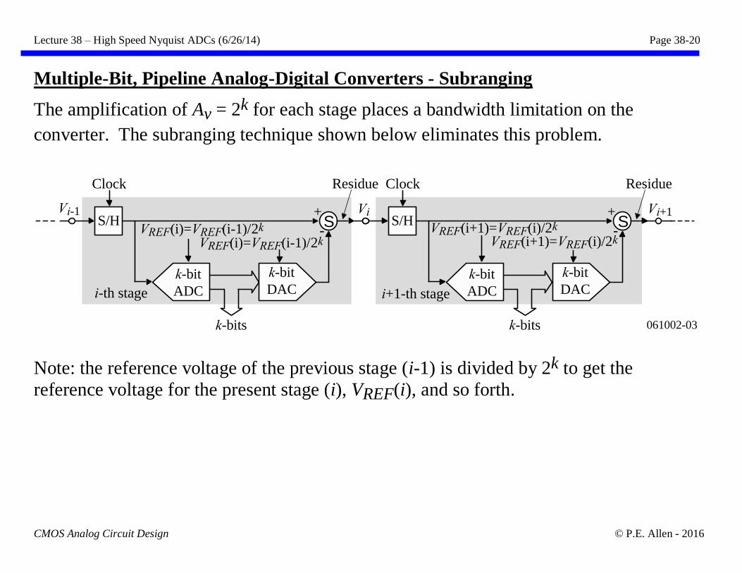
Multiple-Bit, Pipeline Analog-Digital Converters - Subranging
The amplification of Av = 2k for each stage places a bandwidth limitation on the
converter. The subranging technique shown below eliminates this problem.
Note: the reference voltage of the previous stage (i-1) is divided by 2k to get the
reference voltage for the present stage (i), VREF(i), and so forth.
061002-03
k-bit
ADC
k-bit
DAC
k-bits
S/HVREF(i)=VREF(i-1)/2k S
+
-
i-th stage
Vi-1
Clock
Vi
Residue
k-bit
ADC
k-bit
DAC
k-bits
S/H S+
-
i+1-th stage
Clock
Vi+1
Residue
VREF(i+1)=VREF(i)/2k
VREF(i)=VREF(i-1)/2k VREF(i+1)=VREF(i)/2k

Lecture 38 – High Speed Nyquist ADCs (6/26/14) Page 38-21
CMOS Analog Circuit Design © P.E. Allen - 2016
Subranging, Multiple-Bit, Pipeline ADCs
Illustration of a 2-stage, 2-bits/stage pipeline ADC:
Comments:
• Resolution of the
comparators for the
following stages increases
but fortunately, the
tolerance of each stage
decreases by 2k for every
additional stage.
• Removes the frequency
limitation of the amplifier
00011011
11
VREF
0
Stage 2Stage 1
Time
Vo
ltag
e0.5000VREF
0.7500VREF
0.2500VREF
0.3750VREF0.3125VREF
0.4375VREF
Clock 1 Clock 2
Digital output word = 01 10 Fig.10.8-15
00
10
01

Lecture 38 – High Speed Nyquist ADCs (6/26/14) Page 38-22
CMOS Analog Circuit Design © P.E. Allen - 2016
Implementation of the DAC in the Multiple-Bit, Pipeline ADC
Circuit: Comments:
• A good compromise between area and speed
• The ADC does not need to be a flash or
parallel if speed is not crucial
• Typical performance is 10 bits at
50Msamples/sec

Lecture 38 – High Speed Nyquist ADCs (6/26/14) Page 38-23
CMOS Analog Circuit Design © P.E. Allen - 2016
Example 38-2 - Examination of error in subranging for a 2-stage, 2-bits/stage
pipeline ADC
The stages of the 2-stage,
2-bits/stage pipeline ADC
shown below are ideal.
However, the second
stage divides VREF by 2
rather than 4. Find the ±INL and ±DNL for this ADC.
Solution
Examination of the first stage shows that its output, Vout(1) changes at
Vin(1)
VREF =
1
4,
2
4,
3
4, and
4
4 .
The output of the first stage will be Vout(1)
VREF =
b0
2 +
b1
4 .
The second stage changes at Vin(2)
VREF =
1
8,
2
8,
3
8, and
4
8
where
Vin(2) = Vin(1) - Vout(1).
The above relationships permit the information given in the following table.

Lecture 38 – High Speed Nyquist ADCs (6/26/14) Page 38-24
CMOS Analog Circuit Design © P.E. Allen - 2016
Example 38-2 - Continued
Output digital word for Ex. 38-2:
Vin(1)
VREF b0 b1 Vout(1)
VREF
Vin(2)
VREF
b2 b3 Ideal Ouput
b0 b1 b2 b3
0 0 0 0 0 0 0 0 0 0 0
1/16 0 0 0 1/16 0 0 0 0 0 1
2/16 0 0 0 2/16 0 1 0 0 1 0
3/16 0 0 0 3/16 0 1 0 0 1 1
4/16 0 1 4/16 0 0 0 0 1 0 0
5/16 0 1 4/16 1/16 0 0 0 1 0 1
6/16 0 1 4/16 2/16 0 1 0 1 1 0
7/16 0 1 4/16 3/16 0 1 0 1 1 1
8/16 1 0 8/16 0 0 0 1 0 0 0
9/16 1 0 8/16 1/16 0 0 1 0 0 1
10/16 1 0 8/16 2/16 0 1 1 0 1 0
11/16 1 0 8/16 3/16 0 1 1 0 1 1
12/16 1 1 12/16 0 0 0 1 1 0 0
13/16 1 1 12/16 1/16 0 0 1 1 0 1
14/16 1 1 12/16 2/16 0 1 1 1 1 0
15/16 1 1 12/16 3/16 0 1 1 1 1 1
0 1 2 3 4 5 6 7 8 9 10 11 12 13 14 15 1616 16 16 16 16 16 16 16 16 16 16 16 16 16 16 16 16
Analog Input Voltage
0000
0001
0010
0011
0100
0101
0110
0111
1000
1001
1010
1011
1100
1101
1110
1111
Dig
ital
Ou
tpu
t C
ode
Ideal Finite Characteristic
-INL=2LSB
+DNL=2LSB
INL=0LSB
-DNL=0LSB
Comparing the actual digital output word with the ideal output word gives the following:
+INL = 0LSB, -INL = 0111-0101 = -2LSB, +DNL = (1000-0101) - 1LSB = +2LSB,
and -DNL = (0101-0100) - 1LSB = 0LSB.

Lecture 38 – High Speed Nyquist ADCs (6/26/14) Page 38-25
CMOS Analog Circuit Design © P.E. Allen - 2016
Example of a Multiple-Bit, Pipeline ADC
Two-stages with 5-bits per stage resulting in a 10-bit ADC with a sampling rate of
5Msamples/second.
Architecture:
Features:
• Requires only 2n/2-1 comparators
• LSBs decoded using 31 preset charge redistribution capacitor arrays
• Reference voltages used in the LSBs are generated by the MSB ADC
• No op amps are used
S/HMSB
ADC
DACIncrement
by 1
LSB
ADC
DAC
MSBs
LSBs
Vr1
Vr2
Vin Vin*
Fig.10.8-21

Lecture 38 – High Speed Nyquist ADCs (6/26/14) Page 38-26
CMOS Analog Circuit Design © P.E. Allen - 2016
Example of a Multiple-Bit, Pipeline ADC - Continued
MSB Conversion:
Operation:
1.) Sample Vin* on
each 32C
capacitance
autozeroing the
comparators
2.) Connect each
comparator to a node
of the resistor string
generating a
thermometer code.

Lecture 38 – High Speed Nyquist ADCs (6/26/14) Page 38-27
CMOS Analog Circuit Design © P.E. Allen - 2016
Example of a Multiple-Bit, Pipeline ADC - Continued
LSB Conversion: Operation:
1.) MSB comparators are preset to each
of the 31 possible digital codes.
2.) Vr1 and Vr2 are derived from the
MSB conversion.
3.) Preset comparators will produce a
thermometer code to the encoder.
Comments:
• Requires two full clock cycles
• Reuses the comparators
• Accuracy limited by resistor string
and its dynamic loading
• Accuracy also limited by the capacitor
array
• Comparator is a 3-stage, low-gain,
wide-bandwidth, using internal
autozeroing

Lecture 38 – High Speed Nyquist ADCs (6/26/14) Page 38-28
CMOS Analog Circuit Design © P.E. Allen - 2016
Digital Error Correction
Like many of the accuracy enhancing techniques, there are particular applications where
certain correcting techniques are useful. In the pipeline, analog-digital converter, a
technique called digital error correction is used to remove the imperfections of the
components.
Pipeline ADC:
Operation:
1.) Stage 1 resolves the analog input signal to within one of B subranges which
determines the first B bits.
2.) Stage 1 then creates the analog residue (analog input – quantized analog output) and
passes on to Stage 2 by either amplifying or subranging.
3.) Stage 2 repeats this process which ends with Stage K.
Stage 1
B bitsvIN* Stage 2
B bits
Stage K
B bits
KB
bitsDigital
Logic
041007-11

Lecture 38 – High Speed Nyquist ADCs (6/26/14) Page 38-29
CMOS Analog Circuit Design © P.E. Allen - 2016
Example of Digital Error Correction in a Pipeline ADC
Subranging Pipeline ADC Example (B =2, K = 3) using Digital Error Correction.
No correction (error in first comparator): Digital error correction (extra bit in stage 2):
Comments:
• Adds a correcting bit to the following stage to correct for errors in the previous stage.
• The subranging or amplification of the next stage does not include the correcting bit.
• Correction can be done after all stages of the pipeline ADC have converted or after
each individual stage.

Lecture 38 – High Speed Nyquist ADCs (6/26/14) Page 38-30
CMOS Analog Circuit Design © P.E. Allen - 2016
12-Bit Pipeline ADC with Digital Error Correction & Self-Calibration†
Digital Error
Correction:
• Avoids saturation
of the next stage
• Reduces the
number of
missing codes
• Relaxed
specifications for
the comparators
• Compensates for
wrong decisions
in the coarse quantizers
Self-Calibration:
• Can calibrate the effects of the DAC nonlinearity and gain error
• Can be done by digital or analog methods or both
† J. Goes, et. al., CICC’96
DAC
ADC
S/Hvin
3 bits
DAC
ADC
3 bits
DAC
ADC
3 bits
DAC
ADC
3 bits
ADC
4 bits
12 bits
Digital Error Correction Logic
Clock
Fig. 11-30

Lecture 38 – High Speed Nyquist ADCs (6/26/14) Page 38-31
CMOS Analog Circuit Design © P.E. Allen - 2016
TIME-INTERLEAVED ADC CONVERTERS
Time-Interleaved Analog-Digital Converters
Slower ADCs are used in parallel for area reduction or fast ADCs in parallel for speed.
Illustration:
Comments:
• Can get the same throughput with less chip area
• If M = N, then a digital word is converted at every clock cycle
• Multiplexer and timing become challenges at high speeds
• Channels must be matched with ±0.5LSB for delay, gain, and offset.
S/H N-bit ADC No. 1
T1
S/H
T2
S/H
TM
Vin
Digital
word
out
T1 T2 TM T1+TCt
T2+TC TM+TC
N-bit ADC No. 2
N-bit ADC No. M
N-bit ADC No. 1N-bit ADC No. 2
N-bit ADC No. M
T=TC
M
Fig.10.8-20

Lecture 38 – High Speed Nyquist ADCs (6/26/14) Page 38-32
CMOS Analog Circuit Design © P.E. Allen - 2016
SUMMARY
Type of ADC Primary Advantage Primary Disadvantage
Flash or parallel Fast Area is large if N > 6
Interpolating Fast Requires accurate
interpolation
Folding Fast Bandwidth increases if
no S/H used
Multiple-Bit,
Pipeline
Increased number of bits Slower than flash
Time-
interleaved
Small area with large
throughput
Precise timing and fast
multiplexer
Typical Performance:
• 6-8 bits
• 500-2000 Msamples/sec.
• The ENOB at the Nyquist frequency is typically 1-2 bits less that the ENOB at low
frequencies.
• Power is approximately 0.3 to 1W